WO2022168585A1 - Capacitive sensor - Google Patents
Capacitive sensor Download PDFInfo
- Publication number
- WO2022168585A1 WO2022168585A1 PCT/JP2022/001418 JP2022001418W WO2022168585A1 WO 2022168585 A1 WO2022168585 A1 WO 2022168585A1 JP 2022001418 W JP2022001418 W JP 2022001418W WO 2022168585 A1 WO2022168585 A1 WO 2022168585A1
- Authority
- WO
- WIPO (PCT)
- Prior art keywords
- substrate
- frame
- capacitive sensor
- anchor
- elastic
- Prior art date
Links
- 239000000758 substrate Substances 0.000 claims abstract description 244
- 238000001514 detection method Methods 0.000 claims description 76
- XUIMIQQOPSSXEZ-UHFFFAOYSA-N Silicon Chemical compound [Si] XUIMIQQOPSSXEZ-UHFFFAOYSA-N 0.000 claims description 23
- 229910052710 silicon Inorganic materials 0.000 claims description 23
- 239000010703 silicon Substances 0.000 claims description 23
- 239000000463 material Substances 0.000 claims description 19
- 230000008859 change Effects 0.000 claims description 6
- 230000005489 elastic deformation Effects 0.000 abstract description 4
- 244000126211 Hericium coralloides Species 0.000 description 31
- 235000012431 wafers Nutrition 0.000 description 8
- 238000004519 manufacturing process Methods 0.000 description 7
- 230000001133 acceleration Effects 0.000 description 6
- 230000002093 peripheral effect Effects 0.000 description 6
- 239000002184 metal Substances 0.000 description 5
- 125000006850 spacer group Chemical group 0.000 description 5
- 238000006073 displacement reaction Methods 0.000 description 4
- 238000005516 engineering process Methods 0.000 description 4
- 210000000988 bone and bone Anatomy 0.000 description 2
- 238000010586 diagram Methods 0.000 description 2
- IJGRMHOSHXDMSA-UHFFFAOYSA-N Atomic nitrogen Chemical compound N#N IJGRMHOSHXDMSA-UHFFFAOYSA-N 0.000 description 1
- VYPSYNLAJGMNEJ-UHFFFAOYSA-N Silicium dioxide Chemical compound O=[Si]=O VYPSYNLAJGMNEJ-UHFFFAOYSA-N 0.000 description 1
- 239000000956 alloy Substances 0.000 description 1
- 229910045601 alloy Inorganic materials 0.000 description 1
- 238000005452 bending Methods 0.000 description 1
- 239000005388 borosilicate glass Substances 0.000 description 1
- 239000003990 capacitor Substances 0.000 description 1
- 238000010276 construction Methods 0.000 description 1
- 229910001873 dinitrogen Inorganic materials 0.000 description 1
- 239000011521 glass Substances 0.000 description 1
- 230000012447 hatching Effects 0.000 description 1
- 239000012535 impurity Substances 0.000 description 1
- 239000012212 insulator Substances 0.000 description 1
- 238000000034 method Methods 0.000 description 1
- 230000004048 modification Effects 0.000 description 1
- 238000012986 modification Methods 0.000 description 1
- 230000008569 process Effects 0.000 description 1
- 239000011347 resin Substances 0.000 description 1
- 229920005989 resin Polymers 0.000 description 1
- 230000035945 sensitivity Effects 0.000 description 1
- 229910052814 silicon oxide Inorganic materials 0.000 description 1
- 230000000087 stabilizing effect Effects 0.000 description 1
- 230000003068 static effect Effects 0.000 description 1
Images


Classifications
-
- B—PERFORMING OPERATIONS; TRANSPORTING
- B81—MICROSTRUCTURAL TECHNOLOGY
- B81B—MICROSTRUCTURAL DEVICES OR SYSTEMS, e.g. MICROMECHANICAL DEVICES
- B81B3/00—Devices comprising flexible or deformable elements, e.g. comprising elastic tongues or membranes
- B81B3/0018—Structures acting upon the moving or flexible element for transforming energy into mechanical movement or vice versa, i.e. actuators, sensors, generators
- B81B3/0021—Transducers for transforming electrical into mechanical energy or vice versa
-
- B—PERFORMING OPERATIONS; TRANSPORTING
- B81—MICROSTRUCTURAL TECHNOLOGY
- B81B—MICROSTRUCTURAL DEVICES OR SYSTEMS, e.g. MICROMECHANICAL DEVICES
- B81B3/00—Devices comprising flexible or deformable elements, e.g. comprising elastic tongues or membranes
-
- G—PHYSICS
- G01—MEASURING; TESTING
- G01C—MEASURING DISTANCES, LEVELS OR BEARINGS; SURVEYING; NAVIGATION; GYROSCOPIC INSTRUMENTS; PHOTOGRAMMETRY OR VIDEOGRAMMETRY
- G01C19/00—Gyroscopes; Turn-sensitive devices using vibrating masses; Turn-sensitive devices without moving masses; Measuring angular rate using gyroscopic effects
- G01C19/56—Turn-sensitive devices using vibrating masses, e.g. vibratory angular rate sensors based on Coriolis forces
- G01C19/5719—Turn-sensitive devices using vibrating masses, e.g. vibratory angular rate sensors based on Coriolis forces using planar vibrating masses driven in a translation vibration along an axis
- G01C19/5733—Structural details or topology
- G01C19/5755—Structural details or topology the devices having a single sensing mass
- G01C19/5762—Structural details or topology the devices having a single sensing mass the sensing mass being connected to a driving mass, e.g. driving frames
-
- G—PHYSICS
- G01—MEASURING; TESTING
- G01P—MEASURING LINEAR OR ANGULAR SPEED, ACCELERATION, DECELERATION, OR SHOCK; INDICATING PRESENCE, ABSENCE, OR DIRECTION, OF MOVEMENT
- G01P15/00—Measuring acceleration; Measuring deceleration; Measuring shock, i.e. sudden change of acceleration
- G01P15/02—Measuring acceleration; Measuring deceleration; Measuring shock, i.e. sudden change of acceleration by making use of inertia forces using solid seismic masses
- G01P15/08—Measuring acceleration; Measuring deceleration; Measuring shock, i.e. sudden change of acceleration by making use of inertia forces using solid seismic masses with conversion into electric or magnetic values
- G01P15/125—Measuring acceleration; Measuring deceleration; Measuring shock, i.e. sudden change of acceleration by making use of inertia forces using solid seismic masses with conversion into electric or magnetic values by capacitive pick-up
-
- H—ELECTRICITY
- H01—ELECTRIC ELEMENTS
- H01L—SEMICONDUCTOR DEVICES NOT COVERED BY CLASS H10
- H01L29/00—Semiconductor devices adapted for rectifying, amplifying, oscillating or switching, or capacitors or resistors with at least one potential-jump barrier or surface barrier, e.g. PN junction depletion layer or carrier concentration layer; Details of semiconductor bodies or of electrodes thereof ; Multistep manufacturing processes therefor
- H01L29/66—Types of semiconductor device ; Multistep manufacturing processes therefor
- H01L29/84—Types of semiconductor device ; Multistep manufacturing processes therefor controllable by variation of applied mechanical force, e.g. of pressure
-
- B—PERFORMING OPERATIONS; TRANSPORTING
- B81—MICROSTRUCTURAL TECHNOLOGY
- B81B—MICROSTRUCTURAL DEVICES OR SYSTEMS, e.g. MICROMECHANICAL DEVICES
- B81B2201/00—Specific applications of microelectromechanical systems
- B81B2201/02—Sensors
- B81B2201/0228—Inertial sensors
-
- B—PERFORMING OPERATIONS; TRANSPORTING
- B81—MICROSTRUCTURAL TECHNOLOGY
- B81B—MICROSTRUCTURAL DEVICES OR SYSTEMS, e.g. MICROMECHANICAL DEVICES
- B81B2203/00—Basic microelectromechanical structures
- B81B2203/03—Static structures
- B81B2203/0307—Anchors
-
- B—PERFORMING OPERATIONS; TRANSPORTING
- B81—MICROSTRUCTURAL TECHNOLOGY
- B81B—MICROSTRUCTURAL DEVICES OR SYSTEMS, e.g. MICROMECHANICAL DEVICES
- B81B2203/00—Basic microelectromechanical structures
- B81B2203/04—Electrodes
Definitions
- the present disclosure relates generally to capacitive sensors, and more particularly to capacitive sensors with moving parts.
- Patent Document 1 an angular velocity sensor including a substrate (first substrate) and a structure provided on the main surface side of the substrate is known.
- the structure includes a movable portion including a weight portion and a frame-shaped portion, an anchor portion, an elastic portion connecting the anchor portion and the frame-shaped portion, and a detection portion. ,have.
- the capacitance changes according to the angular velocity.
- Patent Document 1 describes that the angular velocity sensor may include a chip size package formed using wafer level package technology or the like.
- the angular velocity sensor disclosed in Patent Document 1 when including a chip size package, comprises a first substrate, a structure, and a second substrate facing the first substrate with the structure interposed therebetween.
- a capacitive sensor such as an angular velocity sensor including a first substrate and a second substrate
- the movable portion may be displaced due to stress generated when the second substrate and the structural body are joined during manufacturing.
- a capacitive sensor may have degraded characteristics when the movable portion is displaced during manufacturing.
- An object of the present disclosure is to provide a capacitive sensor capable of improving characteristics.
- a capacitive sensor includes a first substrate, a second substrate, a movable portion, a support portion, and a detection portion.
- the second substrate faces the first substrate in the thickness direction of the first substrate.
- the movable portion is positioned between the first substrate and the second substrate and spaced apart from the first substrate and the second substrate.
- the support portion is positioned between the first substrate and the second substrate, and supports the movable portion so as to vibrate.
- the detection section detects a change in capacitance due to vibration of the movable section.
- the support portion has a first anchor portion, a second anchor portion, a first connection portion, and a second connection portion. The first anchor part is fixed only to the first substrate out of the first substrate and the second substrate.
- the second anchor portion is positioned apart from the first anchor portion in plan view from the thickness direction of the first substrate, and is fixed to the first substrate and the second substrate.
- the first connection portion is separated from the first substrate and the second substrate and connects the first anchor portion and the movable portion.
- the second connecting portion connects the first anchor portion and the second anchor portion.
- the first connecting portion includes an elastically deformable first elastic portion.
- the second connection part includes a second elastic part that is separated from the first substrate and the second substrate and is elastically deformable.
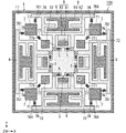
- FIG. 1 is a plan view showing a capacitive sensor according to an embodiment, omitting illustration of a second substrate.
- FIG. 2 is a cross-sectional view taken along the line AA of FIG. 1, showing the same capacitive sensor.
- FIG. 3 is a cross-sectional view taken along the line BB of FIG. 1, showing the same capacitive sensor.
- FIG. 4 shows the same capacitive sensor, which is a cross-sectional view taken along line CC of FIG.
- FIG. 5 is a diagram further schematically illustrating the plan view of FIG. 1, showing the same capacitive sensor.
- FIG. 6 is a schematic cross-sectional view of the capacitive sensor of the same.
- FIG. 1 A capacitive sensor 100 according to an embodiment will be described below with reference to FIGS. 1 to 6.
- FIG. 1 A capacitive sensor 100 according to an embodiment will be described below with reference to FIGS. 1 to 6.
- the capacitive sensor 100 includes a first substrate 1, a second substrate 2, a movable portion 3, a support portion 7, and a detection portion 9. And prepare.
- the second substrate 2 faces the first substrate 1 in the thickness direction D1 of the first substrate 1 .
- the movable part 3 is located between the first substrate 1 and the second substrate 2 and is separated from the first substrate 1 and the second substrate 2 .
- the support portion 7 is positioned between the first substrate 1 and the second substrate 2 and supports the movable portion 3 so as to vibrate.
- a detection unit 9 detects a change in capacitance due to vibration of the movable unit 3 .
- the capacitance is the capacitance of the capacitor that the detection unit 9 has.
- the capacitive sensor 100 is, for example, an angular velocity sensor that converts angular velocity into an electrical signal. That is, the capacitive sensor 100 functions as a transducer that converts angular velocity into an electrical signal.
- the capacitive sensor 100 can be used, for example, in home appliances, mobile terminals, cameras, wearable terminals, game machines, vehicles (including automobiles and motorcycles), robots, construction machinery, drones, aircraft, ships, and the like. .
- the movable portion 3 includes the weight portion 4.
- the capacitive sensor 100 further includes a driving section 8 for driving (vibrating) the weight section 4 .
- the capacitance of the detection section 9 changes according to the angular velocity.
- FIG. 1 Details The configuration of the capacitive sensor 100 according to the embodiment will be described in detail with reference to FIGS. 1 to 6.
- FIG. 1 Details The configuration of the capacitive sensor 100 according to the embodiment will be described in detail with reference to FIGS. 1 to 6.
- orthogonal coordinates having three mutually orthogonal X-, Y-, and Z-axes are defined.
- the axis extending along the vibration (driving) direction of the weight portion 4 is defined as the "X-axis".
- the "Y-axis” is orthogonal to both these Z-axis and X-axis.
- the axis along the vibration (driving) direction of the weight portion 4 is not limited to the X-axis, and may be the Y-axis.
- the X-axis, Y-axis, and Z-axis are all virtual axes, and the arrows indicating "X", "Y", and “Z” in the drawings are merely used for explanation. , none of which is material.
- these directions are not meant to limit the directions during use of the capacitive sensor 100 .
- the origin of the orthogonal coordinates can be defined, for example, at the center of the movable portion 3 (in the example of FIG. 1, the center of the weight portion 4) in plan view from the thickness direction D1 of the first substrate 1.
- the capacitive sensor 100 detects an angular velocity around the Z-axis. Since the Z-axis is an axis along the thickness direction D1 of the first substrate 1 and the thickness direction of the weight portion 4, as a result, the capacitive sensor 100 is static around the central axis of the weight portion 4. As the capacitive sensor 100 rotates, the angular velocity acting on the capacitive sensor 100 is detected as a detection target. That is, the capacitive sensor 100 outputs an electrical signal corresponding to the angular velocity of the weight portion 4 around the central axis. Therefore, it is possible to measure the magnitude of the angular velocity around the center axis (around the Z-axis) of the weight section 4 based on the electric signal output from the capacitance type sensor 100 .
- the first substrate 1 has a square shape in a plan view from the thickness direction D1 of the first substrate 1, it is not limited to this, and may have, for example, a rectangular shape.
- the first substrate 1 includes, for example, a first silicon substrate.
- the second substrate 2 has the same shape as the first substrate 1 when viewed from the thickness direction D1 of the first substrate 1, but may have a different external size.
- the second substrate 2 includes, for example, a second silicon substrate.
- the second substrate 2 includes, for example, an insulating film formed on the main surface of the second silicon substrate opposite to the first substrate 1 side, a plurality of external connection electrodes formed on the insulating film, and a second silicon substrate. 2.
- a plurality of through wires formed along the thickness direction of the silicon substrate and connected to the plurality of external connection electrodes in a one-to-one relationship.
- the plurality of through wires and the second silicon substrate are electrically insulated, for example, by an insulating film interposed between the through wires and the second silicon substrate.
- the plurality of external connection electrodes include external connection electrodes connected to the drive section 8 and external connection electrodes connected to the detection section 9 .
- the support portion 7 has a first anchor portion 71 , a second anchor portion 72 , a first connection portion 76 and a second connection portion 77 .
- the first connecting portion 76 includes a first elastic portion 761 .
- the second connecting portion 77 includes a second elastic portion 771 .
- the first anchor portion 71 is fixed only to the first substrate 1 of the first substrate 1 and the second substrate 2 .
- the second anchor portion 72 is positioned apart from the first anchor portion 71 in plan view from the thickness direction D1 of the first substrate 1 .
- the second anchor portion 72 is fixed to the first substrate 1 and the second substrate 2 .
- the first connecting portion 76 is separated from the first substrate 1 and the second substrate 2 .
- the first connection portion 76 connects the first anchor portion 71 and the movable portion 3 .
- the second connection portion 77 connects the first anchor portion 71 and the second anchor portion 72 .
- the first connecting portion 76 includes an elastically deformable first elastic portion 761 .
- the second connecting portion 77 includes a second elastic portion 771 that is separated from the first substrate 1 and the second substrate 2 and is elastically deformable.
- the drive section 8 has a first drive electrode 81 and a second drive electrode 82 .
- the detection section 9 has a first detection electrode 91 and a second detection electrode 92 .
- components fixed to the first substrate 1 and components not fixed to the first substrate 1 are distinguished by the type of dot hatching. That is, in FIG. , and the components with relatively low dot density (weight portion 4, first connection portion 76, second connection portion 77, frame-shaped portion 6, second drive electrode 82 , second detection electrodes 92 ) are not fixed to the first substrate 1 .
- FIGS. 5 and 6 are schematic diagrams schematically showing the configuration of the capacitive sensor 100, and in FIGS. 5 and 6, the shape and the like of each component may differ from the actual shape and the like.
- the first elastic portion 761 and the second elastic portion 771 are schematically represented by the symbol “spring”, and the actual shapes of the first elastic portion 761 and the second elastic portion 771 are represented by not reflected.
- the direction in which one end and the other end of the "spring" symbol are aligned corresponds to the direction in which elastic deformation is likely to occur.
- the detection target of the capacitive sensor 100 is the angular velocity around the Z-axis (the central axis of the weight portion 4). Therefore, the capacitive sensor 100 outputs an electrical signal corresponding to the angular velocity around the Z-axis.
- the capacitive sensor 100 is a vibrating gyro sensor and detects an angular velocity around the Z-axis using Coriolis force (turning force). In other words, the capacitive sensor 100 senses the Coriolis force generated by an external rotational force acting on the weight 4 while the weight 4 is being vibrated. The angular velocity acting on the portion 4 is detected.
- the weight section 4 is driven and vibrated in the X-axis direction by the electrostatic force generated in the drive section 8 including the first drive electrode 81 and the second drive electrode 82.
- the angular velocity can be detected by the detection unit 9 (the first detection electrode 91 and the second detection electrode 92) in the Y-axis direction.
- the outer peripheral shape of the weight portion 4 is polygonal.
- the capacitive sensor 100 has a plurality (four) of sets each including a frame-shaped portion 6, a first drive electrode 81, a second drive electrode 82, a first detection electrode 91, and a second detection electrode 92, which will be described later.
- the plurality of sets are arranged so that the second drive electrodes 82 face the weight portion 4 outside the weight portion 4 .
- the plurality of sets are arranged so as to have rotational symmetry with the central axis of the weight portion 4 along the thickness direction D1 of the first substrate 1 as the axis of rotation.
- the outer peripheral shape of the first substrate 1 in plan view from the thickness direction D1 of the first substrate 1 is a square shape, it is not limited to this, and may be, for example, a rectangular shape.
- the capacitive sensor 100 has a plurality of (here, four) frame-shaped parts 6 .
- the four frame-shaped portions 6 are arranged so as to surround one weight portion 4 in plan view from the thickness direction D1 of the first substrate 1 .
- one frame-shaped portion 6 is positioned on both sides of the weight portion 4 in the Y-axis direction and both sides in the X-axis direction.
- the weight portion 4 and each frame-shaped portion 6 are separated from each other.
- the frame-shaped portion 6 is aligned with the weight portion 4 in a specified direction orthogonal to the thickness direction D1 of the first substrate 1, and is displaceable in the specified direction.
- the capacitive sensor 100 has a plurality of frame-shaped parts 6 as described above.
- a specified direction aligned with the weight portion 4 is specified for each of the plurality of frame-shaped portions 6, so the specified direction is hereinafter also referred to as a specified direction corresponding to the frame-shaped portion 6. . That is, the prescribed directions corresponding to the frame-shaped portion 6 are different between the frame-shaped portion 6 on the upper side of FIG. 1 and the frame-shaped portion 6 on the left side of FIG.
- Each of the four frame-shaped parts 6 has a rectangular frame shape and includes four frame pieces 61-64.
- the lengths of the two frame pieces 61 and 62 whose length direction is perpendicular to the specified direction in which the frame-shaped portion 6 and weight portion 4 are arranged are the specified direction. It is longer than the length of the two frame pieces 63, 64 in the longitudinal direction. That is, each of the four frame-shaped portions 6 has a length in the direction orthogonal to the prescribed direction that is longer than the length in the prescribed direction. Further, in each of the four frame-shaped portions 6 , the length of the frame piece 61 in the longitudinal direction is longer than the length of the side of the weight portion 4 facing the frame-shaped portion 6 .
- the weight section 4 and each of the four frame-shaped sections 6 are connected by a pair of third elastic sections 5 .
- One end of the pair of third elastic portions 5 is connected to a pair of corners of the weight portion 4, and the other end is the frame piece closest to the weight portion 4 among the four frame pieces 61 to 64 in the frame-shaped portion 6. connected to 61.
- the third elastic portion 5 connects the weight portion 4 and the frame-shaped portion 6, and is elastically deformable in a direction perpendicular to the thickness direction D1 of the first substrate 1 and the defined direction corresponding to the frame-shaped portion 6. be.
- the third elastic portion 5 connected to the upper frame-shaped portion 6 of the four frame-shaped portions 6 in FIG. It has become.
- the third elastic portion 5 connected to the left frame-shaped portion 6 of the four frame-shaped portions 6 in FIG. has become.
- the third elastic portion 5 connected to the lower frame-shaped portion 6 among the four frame-shaped portions 6 in FIG. It has become.
- the rigidity in the X-axis direction is lower than the rigidity in the Y-axis direction and the rigidity in the Z-axis direction.
- the rigidity in the Y-axis direction is lower than the rigidity in the X-axis direction and the rigidity in the Z-axis direction.
- Each of the plurality of third elastic parts 5 is a spring.
- Each of the plurality of third elastic portions 5 has a folded portion 51 .
- the folded portion 51 is U-shaped in plan view from the thickness direction D ⁇ b>1 of the first substrate 1 .
- Each of the plurality of third elastic portions 5 is positioned outside the weight portion 4 in plan view from the thickness direction D1 of the first substrate 1 .
- Each of the four first anchor portions 71 has a substantially quadrangular shape in a plan view from the thickness direction D1 of the first substrate 1 .
- the four first anchor portions 71 are fixed to the first substrate 1 .
- the four first anchor portions 71 are not fixed to the second substrate 2 .
- the four first anchor portions 71 are separated from the second substrate 2 in the thickness direction D1 of the first substrate 1 .
- the four first anchor parts 71 are arranged so as to surround the weight part 4 together with the four frame-shaped parts 6 .
- the four first anchor portions 71 and the four frame-shaped portions 6 are alternately arranged in the direction along the outer peripheral direction of the weight portion 4 .
- two of the four first anchor portions 71 are straight lines including one diagonal line of the square-shaped first substrate 1 in a plan view from the thickness direction D1 of the first substrate 1 .
- the remaining two first anchor portions 71 are arranged on a straight line including the other diagonal line.
- the four first anchor portions 71 are arranged one at each of the four corners of the first substrate 1 .
- the second anchor part 72 is fixed to the first substrate 1 and is also fixed to the second substrate 2 .
- the capacitive sensor 100 has a joint portion 27 (see FIGS. 3 and 4) that joins the second anchor portion 72 and the second substrate 2 .
- the joint portion 27 has conductivity.
- the material of the joint 27 includes metal.
- the joint portion 27 is electrically connected to, for example, a corresponding external connection electrode among the plurality of external connection electrodes of the second substrate 2 via a corresponding through wiring among the plurality of through wirings.
- the second anchor portion 72 and the first anchor portion 71 adjacent to each other are connected by a second connection portion 77 .
- the second connecting portion 77 includes a second elastic portion 771 .
- the above-described first anchor portion 71 is adjacent to the frame-shaped portion 6 in a direction orthogonal to the prescribed direction in which the weight portion 4 and the frame-shaped portion 6 are arranged when viewed from the thickness direction D1 of the first substrate 1 . is doing.
- the second anchor portion 72 is located between the first anchor portion 71 and the weight portion 4 in plan view from the thickness direction D1 of the first substrate 1 and is connected via the first anchor portion 71 and the second connection portion 77 . are connected.
- Each of the four frame-shaped portions 6 described above is supported by each of two adjacent first anchor portions 71 via first elastic portions 761 .
- each of the four frame-shaped portions 6 is connected to one end of the two first elastic portions 761 .
- the other ends of the two first elastic portions 761 are connected to different first anchor portions 71 .
- Each of the four frame-shaped portions 6 can be displaced in a specified direction in which the frame-shaped portion 6 and the weight portion 4 are arranged, and a direction orthogonal to the specified direction and the thickness direction D1 of the first substrate 1. can also be displaced.
- the first elastic portion 761 is not fixed to the first substrate 1 and separated from the main surface 11 of the first substrate 1 . Also, the first elastic portion 761 is not fixed to the second substrate 2 either.
- the first elastic portion 761 connects the first anchor portion 71 and the frame portion 6 that are adjacent to each other. That is, the first anchor portion 71 supports the frame-shaped portion 6 via the first elastic portion 761 .
- the first elastic portion 761 is elastically deformable in a specified direction corresponding to the frame-shaped portion 6 connected to the first elastic portion 761 . For example, two first elastic portions 761 connected to the upper frame-shaped portion 6 of the four frame-shaped portions 6 in FIG. It has an easy structure.
- the rigidity in the Y-axis direction is lower than the rigidity in the X-axis direction and the rigidity in the Z-axis direction.
- the rigidity in the X-axis direction is lower than the rigidity in the Y-axis direction and the rigidity in the Z-axis direction.
- Each of the plurality of first elastic portions 761 is capable of bending (elastic deformation).
- Each of the plurality of first elastic portions 761 has a folded portion 762 in plan view from the thickness direction D1 of the first substrate 1 .
- the folded portion 762 is U-shaped in plan view from the thickness direction D1 of the first substrate 1 .
- Each of the plurality of first elastic portions 761 has one folded portion 762 .
- the first drive electrode 81 is located outside the outer periphery of the frame-shaped portion 6 and is separated from the frame-shaped portion 6 and fixed to the first substrate 1 . Also, the first drive electrode 81 is fixed to the second substrate 2 .
- the capacitive sensor 100 has a joint portion 28 (see FIG. 2) that joins the first drive electrode 81 and the second substrate 2 .
- the joint 28 has electrical conductivity.
- the material of the joint 28 includes metal.
- the material of joint 28 is the same as the material of joint 27 .
- the joint portion 28 is electrically connected to, for example, the corresponding external connection electrode among the plurality of external connection electrodes of the second substrate 2 via the corresponding through wiring among the plurality of through wirings.
- the second drive electrode 82 includes an electrode portion (second comb tooth portion 822 ) located outside the outer periphery of the frame-shaped portion 6 and connected to the frame-shaped portion 6 , and faces the first drive electrode 81 .
- the second drive electrode 82 can be displaced in a prescribed direction corresponding to the frame-shaped portion 6 to which the second drive electrode 82 is connected.
- the second comb tooth portion 822 is displaceable in the X-axis direction
- the second comb tooth portion 822 connected to the lower frame-like portion 6 is displaceable in the Y-axis direction, and is connected to the right frame-like portion 6.
- the second comb tooth portion 822 is displaceable in the X-axis direction.
- the driving section 8 drives the weight section 4 so as to vibrate the weight section 4 .
- the drive section 8 has a first drive electrode 81 and a second drive electrode 82 .
- the drive unit 8 has a function of converting an electric signal (electric quantity) input between the first drive electrode 81 and the second drive electrode 82 into a displacement (mechanical quantity) of the second drive electrode 82 .
- the first drive electrode 81 is a comb-shaped electrode, and in plan view from the thickness direction D1 of the first substrate 1, a first comb rib portion 811 facing the frame portion 6 and a first comb rib portion. and a plurality of first comb tooth portions 812 extending from 811 toward the frame-shaped portion 6 .
- the second drive electrode 82 is a comb-shaped electrode, and the portion of the frame-shaped portion 6 facing the first comb rib portion 811 (frame piece 61 a second comb rib portion 821 configured by a portion of the comb rib portion 821, a plurality of second comb tooth portions 822 (electrode portions) extending from the second comb rib portion 821 in a direction approaching the first comb rib portion 811, including.
- the plurality of first comb teeth 812 and the plurality of second comb teeth 822 are the same as the first comb ribs 811 and the second comb teeth 811 and 822 in plan view from the thickness direction D ⁇ b>1 of the first substrate 1 . They are alternately spaced apart one by one in the direction orthogonal to the direction in which they face the bone portion 821 . That is, the adjacent first comb tooth portion 812 and second comb tooth portion 822 face each other with a gap therebetween.
- the detector 9 outputs an electrical signal related to the movement of the weight 4 when a rotational force (angular velocity) acts on the weight 4 from the outside, thereby outputting an electrical signal corresponding to the angular velocity to be detected.
- the detection section 9 has the first detection electrode 91 and the second detection electrode 92 as described above.
- the detection unit 9 has a function of converting the displacement (mechanical quantity) of the second detection electrode 92 with respect to the first detection electrode 91 into an electric signal (electric quantity) between the first detection electrode 91 and the second detection electrode 92.
- the first detection electrode 91 is positioned inside the outer periphery of the frame-shaped portion 6 and fixed to the first substrate 1 .
- the capacitive sensor 100 also has a joint portion 29 (see FIG. 2) that joins the first detection electrode 91 and the second substrate 2 .
- the joint portion 29 has conductivity.
- the material of the joint 29 includes metal.
- the material of joint 29 is the same as the material of joint 27 .
- the joint portion 29 is electrically connected to, for example, the corresponding external connection electrode among the plurality of external connection electrodes of the second substrate 2 via the corresponding through wiring among the plurality of through wirings.
- the second detection electrode 92 includes an electrode portion (second comb tooth portion 922 ) located inside the outer circumference of the frame-shaped portion 6 and connected to the frame-shaped portion 6 , and faces the first detection electrode 91 .
- the second detection electrode 92 can be displaced in a specified direction corresponding to the frame-shaped portion 6 to which the second detection electrode 92 is connected.
- the electrode portion (second comb tooth portion 922) connected to the upper frame-shaped portion 6 can be displaced in the Y-axis direction.
- the electrode portion (second comb tooth portion 922) connected to the left frame-shaped portion 6 of the four frame-shaped portions 6 in FIG. 1 can be displaced in the X-axis direction.
- the second comb tooth portion 922 connected to the lower frame-shaped portion 6 among the four frame-shaped portions 6 in FIG. 1 can be displaced in the Y-axis direction.
- the electrode portion (the second comb tooth portion 922) connected to the right frame-shaped portion 6 of the four frame-shaped portions 6 in FIG. 1 can be displaced in the X-axis direction.
- the first detection electrode 91 has a comb shape when viewed from the thickness direction D1 of the first substrate 1 .
- the first detection electrode 91 includes a first comb rib portion 911 arranged along the direction in which the weight portion 4 and the frame portion 6 are arranged in plan view from the thickness direction D1 of the first substrate 1 . , a plurality of (four in the illustrated example) extending from the first comb rib portion 911 in a direction approaching portions (frame pieces 63 and 64) of the frame portion 6 facing the first comb rib portion 911. and a first comb tooth portion 912 .
- the four first comb tooth portions 912 are arranged in two first comb tooth portions 912 extending in a direction approaching one frame piece 63 of the four frame pieces 61 to 64 of the frame-shaped portion 6 and at the frame piece 64. and two first comb teeth 912 extending toward each other.
- the second detection electrode 92 includes a base portion 921 configured by the frame-shaped portion 6, and a plurality of (three in the illustrated example) extending from the base portion 921 in a direction approaching the first comb rib portion 911 of the first detection electrode 91. and a second comb tooth portion 922 of. That is, in the capacitive sensor 100, the frame-shaped portion 6 also serves as part of the second detection electrode 92 (base portion 921). In the second detection electrode 92 , one second comb tooth portion 922 extends from each of the two frame pieces 63 and 64 of the frame portion 6 toward the first comb rib portion 911 . In addition, in the second detection electrode 92, each of the two frame pieces 61 and 62 also serves as the second comb tooth portion 922 extending from each of the two frame pieces 63 and 64. As shown in FIG.
- the plurality of first comb teeth 912 and the plurality of second comb teeth 912 are arranged in a direction perpendicular to the direction in which the first comb teeth 912 extend.
- the comb tooth portions 922 are alternately spaced apart one by one.
- the second combteeth portion 922 is formed by combining this second combteeth portion 922 and the first combteeth portion 912 farther from the weight portion 4 among the two first combteeth portions 912 adjacent to this second combteeth portion 922 .
- the distance between the second comb tooth portion 922 and the first comb tooth portion 912 of the two first comb tooth portions 912 that are closer to the weight portion 4 is longer than the distance between them.
- the movable part 3 further has the protruding part 65 .
- the protruding portion 65 protrudes from the frame-shaped portion 6 toward the first anchor portion 71 adjacent to the frame-shaped portion 6 .
- the first anchor portion 71 has a recess 75 into which the protruding portion 65 is inserted. There is a gap between the projecting portion 65 and the recessed portion 75 in plan view from the thickness direction D ⁇ b>1 of the first substrate 1 .
- the projecting portion 65 is not fixed to the first substrate 1 .
- the projecting portion 65 is not fixed to the second substrate 2 either.
- the amount of displacement of the frame-shaped portion 6 is limited by contact between the protrusion 65 and the inner surface of the recess 75 when the frame-shaped portion 6 is displaced with the vibration of the weight 4. be done.
- the weight portion 4, the eight third elastic portions 5, the four frame-shaped portions 6, the four second drive electrodes 82, the four second detection electrodes 92, and the eight first elastic portions 761 , four first anchor portions 71, eight second elastic portions 771, and four second anchor portions 72 are integrated. Also, in the capacitive sensor 100, the four first drive electrodes 81 and the four first detection electrodes 91 are independent.
- the weight portion 4, the eight third elastic portions 5, the eight first elastic portions 761, the eight second elastic portions 771, the four frame-shaped portions 6, and the eight protruding portions 65 , the four second drive electrodes 82 and the four second detection electrodes 92 have the same dimension in the Z-axis direction along the thickness direction D1 of the first substrate 1 .
- the four first anchor portions 71, the four second anchor portions 72, the four first drive electrodes 81, and the four first detection electrodes 91 are formed by the thickness of the first substrate 1. The dimensions in the Z-axis direction along the longitudinal direction D1 are the same.
- the capacitive sensor 100 further includes a frame-shaped spacer portion 10 positioned between the outer peripheral portion of the first substrate 1 and the outer peripheral portion of the second substrate 2 .
- the spacer portion 10 is fixed to the first substrate 1 .
- the spacer portion 10 is fixed to the second substrate 2 .
- the capacitive sensor 100 has a joint portion 20 (see FIGS. 2 to 4 and 6) that joins the spacer portion 10 and the second substrate 2 together.
- the joint portion 20 When viewed from the thickness direction D ⁇ b>1 of the first substrate 1 , the joint portion 20 has a rectangular frame shape along the outer edge of the first substrate 1 .
- the joint portion 20 has conductivity.
- the material of the joint 20 includes metal.
- the material of joint 20 is the same as the material of joint 27 .
- the components other than the second substrate 2 and the junctions 20, 27 to 29, for example, use SOI (Silicon on Insulator) wafers using MEMS (Micro Electro Mechanical Systems) manufacturing technology. It is formed by An SOI wafer has a silicon substrate, an insulating layer (eg, buried oxide) formed on the silicon substrate, and a silicon layer formed on the insulating layer.
- An SOI wafer has a silicon substrate, an insulating layer (eg, buried oxide) formed on the silicon substrate, and a silicon layer formed on the insulating layer.
- a part of the silicon substrate of the SOI wafer constitutes the first substrate 1 (first silicon substrate), and a part of the silicon layer constitutes the weight 4 and the eight third substrates.
- the above-described silicon layer contains impurities, and includes the weight portion 4, the eight third elastic portions 5, the four frame-shaped portions 6, the four second drive electrodes 82, the four second detection electrodes 92, and the eight third elastic portions.
- the one elastic portion 761, the four first anchor portions 71, the eight second elastic portions 771, the four second anchor portions 72, the four first drive electrodes 81, and the four first detection electrodes 91 are electrically conductive. have sex.
- a plurality of components (first anchor portion 71, second anchor portion 72, first drive electrode 81, first detection electrode 91, etc.) fixed to the first substrate 1 ) and main surface 11 of first substrate 1, insulating portion 13 is interposed.
- each insulating portion 13 is composed of a portion of the insulating layer of the SOI wafer. That is, the material of each insulating portion 13 is silicon oxide.
- a plurality of components fixed to the first substrate 1 are fixed to the first substrate 1 via the insulating portion 13 .
- each of the plurality of supporting parts 7 has two second elastic parts 771 .
- the two second elastic portions 771 are arranged symmetrically about one imaginary straight line VL1 (see FIG. 1) along the direction in which the first anchor portions 71 and the second anchor portions 72 are arranged.
- the internal space of the package composed of the first substrate 1, the spacer section 10, and the second substrate 2 is, for example, a nitrogen gas atmosphere or a reduced pressure atmosphere (vacuum).
- the capacitive sensor 100 has a Coriolis force acting on the weight 4 (turning force) while the weight 4 is vibrated in the X-axis direction. force) to detect the angular velocity around the Z-axis.
- the first detection electrode 91 and the second detection electrode 92 in the detection section 9 corresponding to each of the two frame-shaped portions 6 vibrate.
- the gap length between This change in gap length is output to the processing circuitry as a change in capacitance.
- an electrical signal corresponding to the angular velocity around the Z axis acting on (the weight portion 4 of) the capacitive sensor 100 is output from the detection portion 9 (the first detection electrode 91 and the second detection electrode 92). It will be.
- a detection unit 9 adjacent to the driving unit 8 to which voltage is input can be used to monitor the displacement during driving.
- the capacitive sensor 100 is used, for example, electrically connected to a signal processing device.
- the signal processing device is, for example, an ASIC (Application Specific Integrated Circuit).
- a signal processor includes, for example, a driver circuit and a processing circuit.
- the drive circuit provides a drive voltage signal to the capacitive sensor 100 .
- the processing circuit processes the electrical signal output from the capacitive sensor 100 .
- the processing circuit converts an analog electric signal (analog signal) output from the capacitive sensor 100 into a digital signal and performs appropriate arithmetic processing to obtain the angular acceleration around the Z axis. It is possible.
- the support portion 7 includes the first anchor portion 71, the second anchor portion 72, the first connection portion 76, and the second connection portion 77. have.
- the first anchor portion 71 is fixed only to the first substrate 1 out of the first substrate 1 and the second substrate 2
- the second anchor portion 72 is fixed to the first substrate 1 and the second substrate. 2 is fixed.
- the first connection portion 76 is separated from the first substrate 1 and the second substrate 2, and connects the first anchor portion 71 and the movable portion 3, and the second connection portion 77 is the first anchor portion. 71 and the second anchor portion 72 are connected.
- the first connection portion 76 includes an elastically deformable first elastic portion 761
- the second connection portion 77 is separated from the first substrate 1 and the second substrate 2 and is elastically deformable second elastic portion 761 .
- An elastic portion 771 is included.
- the stress generated when the second substrate 2 and the support portion 7 are joined during manufacturing causes the movable portion 3 and the first substrate 1 or the second substrate 2 to It is possible to suppress the occurrence of sticking, and to improve the manufacturing yield.
- the outer peripheral shape of the weight portion 4 in plan view from the thickness direction D1 of the first substrate 1 is not limited to a polygonal shape, and may be, for example, a circular shape.
- the structure including the first substrate 1, the movable portion 3, and the support portion 7 is not limited to being formed using an SOI wafer. may be formed using MEMS manufacturing technology, anodic bonding technology, or the like.
- the material of the glass wafer is borosilicate glass, for example.
- the second connection portion 77 of the support portion 7 only needs to include the second elastic portion 771 . and a fourth elastic portion connecting the third anchor portion and the first anchor portion 71 .
- the structure including the first substrate 1, the movable portion 3, and the support portion 7 is not limited to being manufactured using an SOI wafer. may be formed by In this case, for example, the first anchor portion 71 may be fixed only to the second substrate 2 out of the first substrate 1 and the second substrate 2 .
- the shapes of the first elastic portion 761, the second elastic portion 771, and the third elastic portion 5 are not limited to the illustrated examples.
- first elastic portion 761, the second elastic portion 771, and the third elastic portion 5 are not limited to springs, and may be elastic bodies. Also, the respective numbers of the first elastic portions 761, the second elastic portions 771, and the third elastic portions 5 may be changed as appropriate.
- the material of the first elastic portion 761, the second elastic portion 771 and the third elastic portion 5 is not limited to silicon, and may be metal, alloy, conductive resin, or the like, for example.
- the frame-shaped portion 6 is not limited to a frame that is completely closed when viewed from the thickness direction D1 of the first substrate 1, and may be a partially cut frame shape. It may be U-shaped. Further, the plurality of frame-shaped portions 6 are not limited to having the same shape, and may have different shapes.
- the capacitive sensor 100 may include a plurality of weights 4, like the angular velocity sensor disclosed in Patent Document 1.
- the capacitive sensor 100 is not limited to an angular velocity sensor, and may be, for example, an acceleration sensor or a sensor capable of detecting both angular velocity and acceleration.
- the acceleration sensor is not limited to a double-supported acceleration sensor, and may be a cantilevered acceleration sensor.
- a capacitive sensor (100) includes a first substrate (1), a second substrate (2), a movable portion (3), a support portion (7), and a detection portion (9).
- the second substrate (2) faces the first substrate (1) in the thickness direction (D1) of the first substrate (1).
- the movable part (3) is located between the first substrate (1) and the second substrate (2) and is spaced apart from the first substrate (1) and the second substrate (2).
- the support portion (7) is positioned between the first substrate (1) and the second substrate (2), and supports the movable portion (3) so as to vibrate.
- a detector (9) detects a change in capacitance due to vibration of the movable part (3).
- the support portion (7) has a first anchor portion (71), a second anchor portion (72), a first connection portion (76) and a second connection portion (77).
- the first anchor part (71) is fixed only to the first substrate (1) out of the first substrate (1) and the second substrate (2).
- the second anchor part (72) is located apart from the first anchor part (71) in plan view from the thickness direction (D1) of the first substrate (1). 2 substrate (2).
- the first connection part (76) is separated from the first substrate (1) and the second substrate (2) and connects the first anchor part (71) and the movable part (3).
- the second connecting portion (77) connects the first anchor portion (71) and the second anchor portion (72).
- the first connection part (76) includes an elastically deformable first elastic part (761).
- the second connection part (77) includes a second elastic part (771) that is separated from the first substrate (1) and the second substrate (2) and is elastically deformable.
- the capacitive sensor (100) according to the first aspect can improve its characteristics.
- the capacitive sensor (100) according to the second aspect, in the first aspect, further comprises a joint (27).
- the joint portion (27) is interposed between the second substrate (2) and the second anchor portion (72) and joins the second substrate (2) and the second anchor portion (72).
- the capacitive sensor (100) it is possible to determine the gap length between the movable part (3) and the second substrate (2) by the thickness of the joint part (27).
- the junction (27) has conductivity.
- the junction (27) as part of the wiring.
- a capacitive sensor (100) in any one of the first to third aspects, further comprises an insulating part (13).
- the insulating portion (13) is interposed between the first substrate (1) and the second anchor portion (72).
- the first substrate (1) is a silicon substrate.
- the material of the second anchor portion (72) includes silicon.
- the capacitive sensor (100) according to the fourth aspect can electrically insulate the first substrate (1) and the second anchor portion (72).
- the first elastic portion (761) and the second elastic portion (771) have conductivity .
- the capacitive sensor (100) according to the fifth aspect can use each of the first elastic portion (761) and the second elastic portion (771) as wiring.
- a capacitive sensor (100) according to a sixth aspect is, in the fifth aspect, The material of (77) contains silicon.
- the capacitive sensor (100) according to the sixth aspect can simplify the manufacturing process.
- a capacitive sensor (100) according to a seventh aspect includes a plurality of support portions (7) in any one of the first to sixth aspects.
- a plurality of support portions (7) are arranged so as to have rotational symmetry with respect to the center of the movable portion (3).
- the capacitive sensor (100) according to the seventh aspect can further suppress the inclination of the movable part (3).
- the supporting portion (7) has two second elastic portions (771).
- the two second elastic portions (771) are arranged symmetrically about one imaginary straight line (VL1) along the direction in which the first anchor portion (71) and the second anchor portion (72) are arranged. ing.
- the capacitive sensor (100) according to the eighth aspect can further suppress the inclination of the movable part (3).
- the capacitive sensor (100) according to the ninth aspect, in any one of the first to eighth aspects, further comprises a driving section (8).
- the driving part (8) is located between the first substrate (1) and the second substrate (2) and drives the movable part (3).
- a capacitive sensor (100) is the ninth aspect, wherein the movable part (3) includes a weight part (4), a frame-shaped part (6), a third elastic part (5 ) and The frame-shaped part (6) is located between the first substrate (1) and the second substrate (2), and is a weight part ( 4) and can be displaced in a prescribed direction.
- the third elastic portion (5) is located between the first substrate (1) and the second substrate (2), connects the weight portion (4) and the frame portion (6), and It can be elastically deformed in a direction orthogonal to the thickness direction (D1) of (1) and the prescribed direction.
- the drive section (8) has a first drive electrode (81) and a second drive electrode (82).
- the first drive electrode (81) is located outside the frame-shaped part (6), is separated from the frame-shaped part (6), and is fixed to the first substrate (1).
- the second drive electrode (82) includes an electrode portion (second comb-teeth portion 822) located outside the frame-shaped portion (6) and connected to the frame-shaped portion (6). ) and can be displaced in a prescribed direction.
- the detection section (9) has a first detection electrode (91) and a second detection electrode (92).
- the first detection electrode (91) is located inside the frame (6) and fixed to the first substrate (1).
- the second detection electrode (92) includes an electrode portion (second comb-teeth portion 922) located inside the frame-shaped portion (6) and connected to the frame-shaped portion (6). ) and can be displaced in a prescribed direction.
- a first drive electrode (81) and a second drive electrode are provided between the frame-shaped portion (6) and the weight portion (4) in the prescribed direction. (82) electrode portion (second comb tooth portion 822) is located.
- the capacitive sensor (100) according to the tenth aspect can achieve high sensitivity while achieving miniaturization.
- the configurations according to the second to tenth aspects are not essential configurations for the capacitive sensor (100), and can be omitted as appropriate.
Abstract
Description
以下では、実施形態に係る静電容量型センサ100について、図1~6に基づいて説明する。 (embodiment)
A
実施形態に係る静電容量型センサ100は、図1~6に示すように、第1基板1と、第2基板2と、可動部3と、支持部7と、検出部9と、を備える。第2基板2は、第1基板1の厚さ方向D1において第1基板1に対向している。可動部3は、第1基板1と第2基板2との間において第1基板1及び第2基板2から離れて位置している。支持部7は、第1基板1と第2基板2との間に位置しており、可動部3を振動可能に支持している。検出部9は、可動部3の振動による静電容量の変化を検出する。静電容量は、検出部9の有するキャパシタの静電容量である。 (1) Overview As shown in FIGS. 1 to 6, the
実施形態に係る静電容量型センサ100の構成について、図1~6を参照して詳細に説明する。 (2) Details The configuration of the
静電容量型センサ100は、上述のように、第1基板1と、第2基板2と、可動部3と、支持部7と、駆動部8と、検出部9と、を備える。 (2.1) Overall configuration of
実施形態に係る静電容量型センサ100は、例えば、錘部4をX軸方向に振動させた状態で、錘部4に作用するコリオリ力(転向力)を利用して、Z軸周りの角速度を検知する。 (2.2) Operation of Capacitive Sensor The
実施形態に係る静電容量型センサ100では、支持部7が、第1アンカー部71と、第2アンカー部72と、第1接続部76と、第2接続部77と、を有する。支持部7では、第1アンカー部71が、第1基板1と第2基板2とのうち第1基板1のみに固定されており、第2アンカー部72が、第1基板1と第2基板2とに固定されている。支持部7では、第1接続部76が第1基板1及び第2基板2から離れており、第1アンカー部71と可動部3とをつないでおり、第2接続部77が第1アンカー部71と第2アンカー部72とをつないでいる。支持部7では、第1接続部76が、弾性変形可能な第1弾性部761を含み、第2接続部77が、第1基板1及び第2基板2から離れており弾性変形可能な第2弾性部771を含んでいる。これにより、実施形態に係る静電容量型センサ100は、特性の向上を図ることが可能となる。より詳細には、実施形態に係る静電容量型センサ100では、支持部7と第2基板2を接合するときに発生する応力の可動部3への影響を低減することができるため、錘部4に角速度が作用していない状態において可動部3が第1基板1の主面11に対して傾くことを抑制でき、可動部3(の錘部4)の振動を安定化することが可能となり、特性の向上を図ることが可能となる。 (3) Advantages In the
上記の実施形態は、本開示の様々な実施形態の一つに過ぎない。上記の実施形態は、本開示の目的を達成できれば、設計等に応じて種々の変更が可能である。 (Modification)
The embodiment described above is but one of the various embodiments of the present disclosure. The above-described embodiment can be modified in various ways according to design and the like, as long as the object of the present disclosure can be achieved.
第1の態様に係る静電容量型センサ(100)は、第1基板(1)と、第2基板(2)と、可動部(3)と、支持部(7)と、検出部(9)と、を備える。第2基板(2)は、第1基板(1)の厚さ方向(D1)において第1基板(1)に対向している。可動部(3)は、第1基板(1)と第2基板(2)との間において第1基板(1)及び第2基板(2)から離れて位置している。支持部(7)は、第1基板(1)と第2基板(2)との間に位置しており、可動部(3)を振動可能に支持している。検出部(9)は、可動部(3)の振動による静電容量の変化を検出する。支持部(7)は、第1アンカー部(71)と、第2アンカー部(72)と、第1接続部(76)と、第2接続部(77)と、を有する。第1アンカー部(71)は、第1基板(1)と第2基板(2)とのうち第1基板(1)のみに固定されている。第2アンカー部(72)は、第1基板(1)の厚さ方向(D1)からの平面視で第1アンカー部(71)から離れて位置しており、第1基板(1)と第2基板(2)とに固定されている。第1接続部(76)は、第1基板(1)及び第2基板(2)から離れており、第1アンカー部(71)と可動部(3)とをつないでいる。第2接続部(77)は、第1アンカー部(71)と第2アンカー部(72)とをつないでいる。第1接続部(76)は、弾性変形可能な第1弾性部(761)を含む。第2接続部(77)は、第1基板(1)及び第2基板(2)から離れており弾性変形可能な第2弾性部(771)を含む。 (mode)
A capacitive sensor (100) according to a first aspect includes a first substrate (1), a second substrate (2), a movable portion (3), a support portion (7), and a detection portion (9). ) and The second substrate (2) faces the first substrate (1) in the thickness direction (D1) of the first substrate (1). The movable part (3) is located between the first substrate (1) and the second substrate (2) and is spaced apart from the first substrate (1) and the second substrate (2). The support portion (7) is positioned between the first substrate (1) and the second substrate (2), and supports the movable portion (3) so as to vibrate. A detector (9) detects a change in capacitance due to vibration of the movable part (3). The support portion (7) has a first anchor portion (71), a second anchor portion (72), a first connection portion (76) and a second connection portion (77). The first anchor part (71) is fixed only to the first substrate (1) out of the first substrate (1) and the second substrate (2). The second anchor part (72) is located apart from the first anchor part (71) in plan view from the thickness direction (D1) of the first substrate (1). 2 substrate (2). The first connection part (76) is separated from the first substrate (1) and the second substrate (2) and connects the first anchor part (71) and the movable part (3). The second connecting portion (77) connects the first anchor portion (71) and the second anchor portion (72). The first connection part (76) includes an elastically deformable first elastic part (761). The second connection part (77) includes a second elastic part (771) that is separated from the first substrate (1) and the second substrate (2) and is elastically deformable.
11 主面
13 絶縁部
2 第2基板
27 接合部
28 接合部
29 接合部
3 可動部
4 錘部
5 第3弾性部
51 折り返し部
6 枠状部
65 突出部
7 支持部
71 第1アンカー部
72 第2アンカー部
75 凹部
76 第1接続部
761 第1弾性部
762 折り返し部
77 第2接続部
771 第2弾性部
772 折り返し部
8 駆動部
81 第1駆動電極
811 第1櫛骨部
812 第1櫛歯部
82 第2駆動電極
821 第2櫛骨部
822 第2櫛歯部
9 検出部
91 第1検出電極
911 第1櫛骨部
912 第1櫛歯部
92 第2検出電極
921 基部
922 第2櫛歯部
100 静電容量型センサ
D1 厚さ方向 1
Claims (10)
- 第1基板と、
前記第1基板の厚さ方向において前記第1基板に対向している第2基板と、
前記第1基板と前記第2基板との間において前記第1基板及び前記第2基板から離れて位置している可動部と、
前記第1基板と前記第2基板との間に位置しており、前記可動部を振動可能に支持している支持部と、
前記可動部の振動による静電容量の変化を検出する検出部と、を備え、
前記支持部は、
前記第1基板と前記第2基板とのうち前記第1基板のみに固定されている第1アンカー部と、
前記第1基板の前記厚さ方向からの平面視で前記第1アンカー部から離れて位置しており、前記第1基板と前記第2基板とに固定されている第2アンカー部と、
前記第1基板及び前記第2基板から離れており、前記第1アンカー部と前記可動部とをつないでいる第1接続部と、
前記第1アンカー部と前記第2アンカー部とをつないでいる第2接続部と、を有し、
前記第1接続部は、弾性変形可能な第1弾性部を含み、
前記第2接続部は、前記第1基板及び前記第2基板から離れており弾性変形可能な第2弾性部を含む、
静電容量型センサ。 a first substrate;
a second substrate facing the first substrate in the thickness direction of the first substrate;
a movable portion positioned between the first substrate and the second substrate and spaced apart from the first substrate and the second substrate;
a support portion positioned between the first substrate and the second substrate and supporting the movable portion so as to vibrate;
a detection unit that detects a change in capacitance due to vibration of the movable unit,
The support part is
a first anchor portion fixed only to the first substrate out of the first substrate and the second substrate;
a second anchor portion positioned apart from the first anchor portion in plan view from the thickness direction of the first substrate and fixed to the first substrate and the second substrate;
a first connecting portion that is separated from the first substrate and the second substrate and that connects the first anchor portion and the movable portion;
a second connecting portion connecting the first anchor portion and the second anchor portion;
The first connecting portion includes an elastically deformable first elastic portion,
The second connecting portion includes a second elastic portion that is separated from the first substrate and the second substrate and is elastically deformable,
Capacitive sensor. - 前記第2基板と前記第2アンカー部との間に介在し、前記第2基板と前記第2アンカー部とを接合している接合部を更に備える、
請求項1に記載の静電容量型センサ。 further comprising a joint portion interposed between the second substrate and the second anchor portion and joining the second substrate and the second anchor portion;
The capacitive sensor according to claim 1. - 前記接合部は、導電性を有する、
請求項2に記載の静電容量型センサ。 wherein the junction has electrical conductivity;
The capacitive sensor according to claim 2. - 前記第1基板と前記第2アンカー部との間に介在している絶縁部を更に備え、
前記第1基板は、シリコン基板であり、
前記第2アンカー部の材料は、シリコンを含む、
請求項1~3のいずれか一項に記載の静電容量型センサ。 further comprising an insulating portion interposed between the first substrate and the second anchor portion;
The first substrate is a silicon substrate,
The material of the second anchor part contains silicon,
The capacitive sensor according to any one of claims 1 to 3. - 前記第1弾性部及び前記第2弾性部は、導電性を有する、
請求項1~4のいずれか一項に記載の静電容量型センサ。 The first elastic portion and the second elastic portion have conductivity,
The capacitive sensor according to any one of claims 1-4. - 前記第1アンカー部、前記第2アンカー部、前記第1接続部及び前記第2接続部の材料が、シリコンを含む、
請求項5に記載の静電容量型センサ。 a material of the first anchor portion, the second anchor portion, the first connection portion, and the second connection portion includes silicon;
The capacitive sensor according to claim 5. - 前記支持部を複数備え、
前記複数の支持部は、前記可動部の中心を基準として回転対称性を有するように配置されている、
請求項1~6のいずれか一項に記載の静電容量型センサ。 A plurality of the support parts are provided,
The plurality of support portions are arranged so as to have rotational symmetry with respect to the center of the movable portion.
The capacitive sensor according to any one of claims 1-6. - 前記支持部は、前記第2弾性部を2つ有し、
前記2つの第2弾性部は、前記第1アンカー部と前記第2アンカー部との並んでいる方向に沿った1つの仮想直線を中心として線対称に配置されている、
請求項1~7のいずれか一項に記載の静電容量型センサ。 The support portion has two second elastic portions,
The two second elastic portions are arranged line-symmetrically about one imaginary straight line along the direction in which the first anchor portion and the second anchor portion are arranged.
The capacitive sensor according to any one of claims 1-7. - 前記第1基板と前記第2基板との間に位置しており、前記可動部を駆動する駆動部を更に備える、
請求項1~8のいずれか一項に記載の静電容量型センサ。 A driving unit positioned between the first substrate and the second substrate and configured to drive the movable unit,
The capacitive sensor according to any one of claims 1-8. - 前記可動部は、
錘部と、
前記第1基板と前記第2基板との間に位置し、前記第1基板の前記厚さ方向に直交する規定方向において前記錘部と並んでおり、前記規定方向に変位可能な枠状部と、
前記第1基板と前記第2基板との間に位置し、前記錘部と前記枠状部とをつないでおり、前記第1基板の前記厚さ方向と前記規定方向とに直交する方向に弾性変形可能な第3弾性部と、を有し、
前記駆動部は、
前記枠状部の外側に位置して前記枠状部から離れており、前記第1基板に固定されている第1駆動電極と、
前記枠状部の外側に位置して前記枠状部とつながっている電極部分を含み、前記第1駆動電極に対向しており、前記規定方向に変位可能な第2駆動電極と、を有し、
前記検出部は、
前記枠状部の内側に位置しており、前記第1基板に固定されている第1検出電極と、
前記枠状部の内側に位置して前記枠状部とつながっている電極部分を含み、前記第1検出電極に対向しており、前記規定方向に変位可能な第2検出電極と、を有し、
前記第1基板の前記厚さ方向からの平面視で、前記規定方向において前記枠状部と前記錘部との間に前記第1駆動電極と前記第2駆動電極の前記電極部分とが位置している、
請求項9に記載の静電容量型センサ。 The movable part is
a weight;
a frame-shaped portion positioned between the first substrate and the second substrate, aligned with the weight portion in a specified direction orthogonal to the thickness direction of the first substrate, and displaceable in the specified direction; ,
It is positioned between the first substrate and the second substrate, connects the weight portion and the frame-shaped portion, and is elastic in a direction perpendicular to the thickness direction and the defined direction of the first substrate. a deformable third elastic portion;
The drive unit
a first drive electrode positioned outside the frame-shaped portion and away from the frame-shaped portion and fixed to the first substrate;
a second drive electrode that includes an electrode portion that is located outside the frame-shaped portion and is connected to the frame-shaped portion, faces the first drive electrode, and is displaceable in the prescribed direction. ,
The detection unit is
a first detection electrode positioned inside the frame-shaped portion and fixed to the first substrate;
a second detection electrode that includes an electrode portion that is positioned inside the frame-shaped portion and is connected to the frame-shaped portion, faces the first detection electrode, and is displaceable in the prescribed direction. ,
In a plan view from the thickness direction of the first substrate, the electrode portions of the first drive electrodes and the second drive electrodes are positioned between the frame-shaped portion and the weight portion in the prescribed direction. ing,
The capacitive sensor according to claim 9.
Priority Applications (3)
| Application Number | Priority Date | Filing Date | Title |
|---|---|---|---|
| US18/263,267 US20240092630A1 (en) | 2021-02-04 | 2022-01-17 | Capacitive sensor |
| CN202280010003.6A CN116761980A (en) | 2021-02-04 | 2022-01-17 | capacitive sensor |
| JP2022579420A JPWO2022168585A1 (en) | 2021-02-04 | 2022-01-17 |
Applications Claiming Priority (2)
| Application Number | Priority Date | Filing Date | Title |
|---|---|---|---|
| JP2021-016755 | 2021-02-04 | ||
| JP2021016755 | 2021-02-04 |
Publications (1)
| Publication Number | Publication Date |
|---|---|
| WO2022168585A1 true WO2022168585A1 (en) | 2022-08-11 |
Family
ID=82740694
Family Applications (1)
| Application Number | Title | Priority Date | Filing Date |
|---|---|---|---|
| PCT/JP2022/001418 WO2022168585A1 (en) | 2021-02-04 | 2022-01-17 | Capacitive sensor |
Country Status (4)
| Country | Link |
|---|---|
| US (1) | US20240092630A1 (en) |
| JP (1) | JPWO2022168585A1 (en) |
| CN (1) | CN116761980A (en) |
| WO (1) | WO2022168585A1 (en) |
Citations (5)
| Publication number | Priority date | Publication date | Assignee | Title |
|---|---|---|---|---|
| JPH0918017A (en) * | 1995-06-30 | 1997-01-17 | Omron Corp | Semiconductor acceleration sensor and semiconductor pressure sensor |
| JP2005337874A (en) * | 2004-05-26 | 2005-12-08 | Matsushita Electric Works Ltd | Semiconductor acceleration sensor |
| WO2018135211A1 (en) * | 2017-01-17 | 2018-07-26 | パナソニックIpマネジメント株式会社 | Sensor |
| WO2020203011A1 (en) * | 2019-03-29 | 2020-10-08 | パナソニックIpマネジメント株式会社 | Angular velocity sensor |
| JP2021076424A (en) * | 2019-11-06 | 2021-05-20 | 株式会社豊田中央研究所 | MEMS structure |
-
2022
- 2022-01-17 US US18/263,267 patent/US20240092630A1/en active Pending
- 2022-01-17 WO PCT/JP2022/001418 patent/WO2022168585A1/en active Application Filing
- 2022-01-17 CN CN202280010003.6A patent/CN116761980A/en active Pending
- 2022-01-17 JP JP2022579420A patent/JPWO2022168585A1/ja active Pending
Patent Citations (5)
| Publication number | Priority date | Publication date | Assignee | Title |
|---|---|---|---|---|
| JPH0918017A (en) * | 1995-06-30 | 1997-01-17 | Omron Corp | Semiconductor acceleration sensor and semiconductor pressure sensor |
| JP2005337874A (en) * | 2004-05-26 | 2005-12-08 | Matsushita Electric Works Ltd | Semiconductor acceleration sensor |
| WO2018135211A1 (en) * | 2017-01-17 | 2018-07-26 | パナソニックIpマネジメント株式会社 | Sensor |
| WO2020203011A1 (en) * | 2019-03-29 | 2020-10-08 | パナソニックIpマネジメント株式会社 | Angular velocity sensor |
| JP2021076424A (en) * | 2019-11-06 | 2021-05-20 | 株式会社豊田中央研究所 | MEMS structure |
Also Published As
| Publication number | Publication date |
|---|---|
| JPWO2022168585A1 (en) | 2022-08-11 |
| CN116761980A (en) | 2023-09-15 |
| US20240092630A1 (en) | 2024-03-21 |
Similar Documents
| Publication | Publication Date | Title |
|---|---|---|
| JP5070778B2 (en) | Mechanical quantity sensor | |
| US8739626B2 (en) | Micromachined inertial sensor devices | |
| JP5898283B2 (en) | Micro electromechanical system | |
| CN104094084A (en) | Mems proof mass with split z-axis portions | |
| KR20120043056A (en) | Micromachined inertial sensor devices | |
| WO2008059757A1 (en) | Sensor | |
| JP2023050622A (en) | inertial sensor module | |
| JP2005283428A (en) | Dynamic quantity sensor unit | |
| WO2022168585A1 (en) | Capacitive sensor | |
| JP7365647B2 (en) | angular velocity sensor | |
| JPH1010148A (en) | Attitude sensing chip for semiconductor | |
| JP2014215294A (en) | MEMS element | |
| JP7403069B2 (en) | physical quantity sensor | |
| JP4466283B2 (en) | Gyro sensor | |
| JP6958533B2 (en) | Vibration type sensor device | |
| JP2008232704A (en) | Inertia force sensor | |
| US20240142491A1 (en) | MEMS Device And Inertial Measurement Unit | |
| WO2014061247A1 (en) | Angular velocity sensor | |
| JP2023037517A (en) | sensor device | |
| JP2023162599A (en) | Inertial sensor, and inertial measurement device | |
| JP2023182910A (en) | Acceleration sensor | |
| JP5776184B2 (en) | Sensor device | |
| JP2008261771A (en) | Inertia force sensor | |
| JP2012161855A (en) | Electrostatic capacitance type mems device | |
| JP2010185716A (en) | Angular velocity sensor module |
Legal Events
| Date | Code | Title | Description |
|---|---|---|---|
| 121 | Ep: the epo has been informed by wipo that ep was designated in this application |
Ref document number: 22749461 Country of ref document: EP Kind code of ref document: A1 |
|
| WWE | Wipo information: entry into national phase |
Ref document number: 202280010003.6 Country of ref document: CN |
|
| ENP | Entry into the national phase |
Ref document number: 2022579420 Country of ref document: JP Kind code of ref document: A |
|
| WWE | Wipo information: entry into national phase |
Ref document number: 18263267 Country of ref document: US |
|
| NENP | Non-entry into the national phase |
Ref country code: DE |
|
| 122 | Ep: pct application non-entry in european phase |
Ref document number: 22749461 Country of ref document: EP Kind code of ref document: A1 |