WO2022163353A1 - 発光装置、発光装置の製造方法、および測距装置 - Google Patents
発光装置、発光装置の製造方法、および測距装置 Download PDFInfo
- Publication number
- WO2022163353A1 WO2022163353A1 PCT/JP2022/000729 JP2022000729W WO2022163353A1 WO 2022163353 A1 WO2022163353 A1 WO 2022163353A1 JP 2022000729 W JP2022000729 W JP 2022000729W WO 2022163353 A1 WO2022163353 A1 WO 2022163353A1
- Authority
- WO
- WIPO (PCT)
- Prior art keywords
- light
- substrate
- emitting device
- structures
- light emitting
- Prior art date
- Legal status (The legal status is an assumption and is not a legal conclusion. Google has not performed a legal analysis and makes no representation as to the accuracy of the status listed.)
- Ceased
Links
Images






Classifications
-
- G—PHYSICS
- G01—MEASURING; TESTING
- G01S—RADIO DIRECTION-FINDING; RADIO NAVIGATION; DETERMINING DISTANCE OR VELOCITY BY USE OF RADIO WAVES; LOCATING OR PRESENCE-DETECTING BY USE OF THE REFLECTION OR RERADIATION OF RADIO WAVES; ANALOGOUS ARRANGEMENTS USING OTHER WAVES
- G01S7/00—Details of systems according to groups G01S13/00, G01S15/00, G01S17/00
- G01S7/48—Details of systems according to groups G01S13/00, G01S15/00, G01S17/00 of systems according to group G01S17/00
- G01S7/481—Constructional features, e.g. arrangements of optical elements
- G01S7/4814—Constructional features, e.g. arrangements of optical elements of transmitters alone
-
- G—PHYSICS
- G01—MEASURING; TESTING
- G01B—MEASURING LENGTH, THICKNESS OR SIMILAR LINEAR DIMENSIONS; MEASURING ANGLES; MEASURING AREAS; MEASURING IRREGULARITIES OF SURFACES OR CONTOURS
- G01B11/00—Measuring arrangements characterised by the use of optical techniques
- G01B11/24—Measuring arrangements characterised by the use of optical techniques for measuring contours or curvatures
- G01B11/25—Measuring arrangements characterised by the use of optical techniques for measuring contours or curvatures by projecting a pattern, e.g. one or more lines, moiré fringes on the object
-
- G—PHYSICS
- G01—MEASURING; TESTING
- G01C—MEASURING DISTANCES, LEVELS OR BEARINGS; SURVEYING; NAVIGATION; GYROSCOPIC INSTRUMENTS; PHOTOGRAMMETRY OR VIDEOGRAMMETRY
- G01C3/00—Measuring distances in line of sight; Optical rangefinders
- G01C3/02—Details
- G01C3/06—Use of electric means to obtain final indication
-
- G—PHYSICS
- G01—MEASURING; TESTING
- G01S—RADIO DIRECTION-FINDING; RADIO NAVIGATION; DETERMINING DISTANCE OR VELOCITY BY USE OF RADIO WAVES; LOCATING OR PRESENCE-DETECTING BY USE OF THE REFLECTION OR RERADIATION OF RADIO WAVES; ANALOGOUS ARRANGEMENTS USING OTHER WAVES
- G01S7/00—Details of systems according to groups G01S13/00, G01S15/00, G01S17/00
- G01S7/48—Details of systems according to groups G01S13/00, G01S15/00, G01S17/00 of systems according to group G01S17/00
- G01S7/481—Constructional features, e.g. arrangements of optical elements
-
- G—PHYSICS
- G02—OPTICS
- G02B—OPTICAL ELEMENTS, SYSTEMS OR APPARATUS
- G02B3/00—Simple or compound lenses
-
- G—PHYSICS
- G02—OPTICS
- G02B—OPTICAL ELEMENTS, SYSTEMS OR APPARATUS
- G02B3/00—Simple or compound lenses
- G02B3/02—Simple or compound lenses with non-spherical faces
- G02B3/08—Simple or compound lenses with non-spherical faces with discontinuous faces, e.g. Fresnel lens
-
- G—PHYSICS
- G02—OPTICS
- G02B—OPTICAL ELEMENTS, SYSTEMS OR APPARATUS
- G02B5/00—Optical elements other than lenses
- G02B5/02—Diffusing elements; Afocal elements
-
- G—PHYSICS
- G02—OPTICS
- G02B—OPTICAL ELEMENTS, SYSTEMS OR APPARATUS
- G02B7/00—Mountings, adjusting means, or light-tight connections, for optical elements
- G02B7/02—Mountings, adjusting means, or light-tight connections, for optical elements for lenses
-
- G—PHYSICS
- G02—OPTICS
- G02B—OPTICAL ELEMENTS, SYSTEMS OR APPARATUS
- G02B7/00—Mountings, adjusting means, or light-tight connections, for optical elements
- G02B7/28—Systems for automatic generation of focusing signals
- G02B7/30—Systems for automatic generation of focusing signals using parallactic triangle with a base line
- G02B7/32—Systems for automatic generation of focusing signals using parallactic triangle with a base line using active means, e.g. light emitter
-
- G—PHYSICS
- G02—OPTICS
- G02B—OPTICAL ELEMENTS, SYSTEMS OR APPARATUS
- G02B7/00—Mountings, adjusting means, or light-tight connections, for optical elements
- G02B7/28—Systems for automatic generation of focusing signals
- G02B7/40—Systems for automatic generation of focusing signals using time delay of the reflected waves, e.g. of ultrasonic waves
-
- G—PHYSICS
- G03—PHOTOGRAPHY; CINEMATOGRAPHY; ANALOGOUS TECHNIQUES USING WAVES OTHER THAN OPTICAL WAVES; ELECTROGRAPHY; HOLOGRAPHY
- G03B—APPARATUS OR ARRANGEMENTS FOR TAKING PHOTOGRAPHS OR FOR PROJECTING OR VIEWING THEM; APPARATUS OR ARRANGEMENTS EMPLOYING ANALOGOUS TECHNIQUES USING WAVES OTHER THAN OPTICAL WAVES; ACCESSORIES THEREFOR
- G03B13/00—Viewfinders; Focusing aids for cameras; Means for focusing for cameras; Autofocus systems for cameras
- G03B13/32—Means for focusing
- G03B13/34—Power focusing
- G03B13/36—Autofocus systems
-
- H—ELECTRICITY
- H01—ELECTRIC ELEMENTS
- H01S—DEVICES USING THE PROCESS OF LIGHT AMPLIFICATION BY STIMULATED EMISSION OF RADIATION [LASER] TO AMPLIFY OR GENERATE LIGHT; DEVICES USING STIMULATED EMISSION OF ELECTROMAGNETIC RADIATION IN WAVE RANGES OTHER THAN OPTICAL
- H01S5/00—Semiconductor lasers
- H01S5/02—Structural details or components not essential to laser action
- H01S5/0206—Substrates, e.g. growth, shape, material, removal or bonding
- H01S5/0218—Substrates comprising semiconducting materials from other groups of the Periodic Table than the materials of the active layer
-
- H—ELECTRICITY
- H01—ELECTRIC ELEMENTS
- H01S—DEVICES USING THE PROCESS OF LIGHT AMPLIFICATION BY STIMULATED EMISSION OF RADIATION [LASER] TO AMPLIFY OR GENERATE LIGHT; DEVICES USING STIMULATED EMISSION OF ELECTROMAGNETIC RADIATION IN WAVE RANGES OTHER THAN OPTICAL
- H01S5/00—Semiconductor lasers
- H01S5/10—Construction or shape of the optical resonator, e.g. extended or external cavity, coupled cavities, bent-guide, varying width, thickness or composition of the active region
- H01S5/18—Surface-emitting [SE] lasers, e.g. having both horizontal and vertical cavities
- H01S5/183—Surface-emitting [SE] lasers, e.g. having both horizontal and vertical cavities having only vertical cavities, e.g. vertical cavity surface-emitting lasers [VCSEL]
- H01S5/18305—Surface-emitting [SE] lasers, e.g. having both horizontal and vertical cavities having only vertical cavities, e.g. vertical cavity surface-emitting lasers [VCSEL] with emission through the substrate, i.e. bottom emission
-
- H—ELECTRICITY
- H01—ELECTRIC ELEMENTS
- H01S—DEVICES USING THE PROCESS OF LIGHT AMPLIFICATION BY STIMULATED EMISSION OF RADIATION [LASER] TO AMPLIFY OR GENERATE LIGHT; DEVICES USING STIMULATED EMISSION OF ELECTROMAGNETIC RADIATION IN WAVE RANGES OTHER THAN OPTICAL
- H01S5/00—Semiconductor lasers
- H01S5/10—Construction or shape of the optical resonator, e.g. extended or external cavity, coupled cavities, bent-guide, varying width, thickness or composition of the active region
- H01S5/18—Surface-emitting [SE] lasers, e.g. having both horizontal and vertical cavities
- H01S5/183—Surface-emitting [SE] lasers, e.g. having both horizontal and vertical cavities having only vertical cavities, e.g. vertical cavity surface-emitting lasers [VCSEL]
- H01S5/18386—Details of the emission surface for influencing the near- or far-field, e.g. a grating on the surface
- H01S5/18388—Lenses
-
- H—ELECTRICITY
- H04—ELECTRIC COMMUNICATION TECHNIQUE
- H04N—PICTORIAL COMMUNICATION, e.g. TELEVISION
- H04N23/00—Cameras or camera modules comprising electronic image sensors; Control thereof
- H04N23/56—Cameras or camera modules comprising electronic image sensors; Control thereof provided with illuminating means
-
- H—ELECTRICITY
- H01—ELECTRIC ELEMENTS
- H01S—DEVICES USING THE PROCESS OF LIGHT AMPLIFICATION BY STIMULATED EMISSION OF RADIATION [LASER] TO AMPLIFY OR GENERATE LIGHT; DEVICES USING STIMULATED EMISSION OF ELECTROMAGNETIC RADIATION IN WAVE RANGES OTHER THAN OPTICAL
- H01S5/00—Semiconductor lasers
- H01S5/40—Arrangement of two or more semiconductor lasers, not provided for in groups H01S5/02 - H01S5/30
- H01S5/42—Arrays of surface emitting lasers
- H01S5/423—Arrays of surface emitting lasers having a vertical cavity
Definitions
- the present disclosure relates to a light-emitting device, a method for manufacturing the light-emitting device, and a rangefinder.
- VCSELs Vertical Cavity Surface Emitting Lasers
- a plurality of light-emitting elements are provided in a two-dimensional array on the front or rear surface of a substrate.
- the above light emitting device for example, there are cases where it is desired to shape the light emitted from a plurality of light emitting elements in various ways. For example, there are cases where it is desired to converge light, there are cases where it is desired to diffuse light, and there are cases where it is desired to scatter light. In this case, the question arises as to what method should be used to shape the light.
- the present disclosure provides a light-emitting device capable of suitably shaping light from a plurality of light-emitting elements, a method for manufacturing the light-emitting device, and a distance measuring device.
- a light-emitting device includes a substrate, a plurality of light-emitting elements provided on a first surface of the substrate, and light emitted from the plurality of light-emitting elements provided on a second surface of the substrate. a plurality of structures through which light passes, at least one of the structures includes a first structure through which a first portion of the light passes, and a function different from that of the first structure; and a second structure through which a second portion of the is transparent.
- light from a plurality of light-emitting elements can be favorably shaped, for example, light incident on a corresponding structure from a light-emitting element can be shaped differently between the first structure and the second structure. It becomes possible.
- the first and second structures may have a shape in which the second structure surrounds the first structure in an annular shape.
- a structure that is desirable to be circular can be set as the first structure, and a structure that does not have to be circular can be set as the second structure.
- the interface between the first and second structures may be a plane. This makes it possible to arrange the first and second structures in a simple layout, such as arranging the first and second structures on the left and right, respectively.
- the first structure may be a lens
- the second structure may be a structure other than a lens. This allows, for example, a first structure to focus or diffuse light and a second structure to otherwise shape the light.
- the first structure may be a lens
- the second structure may be a scatterer. This allows, for example, the first structure to focus or diffuse the light and the second structure to scatter the light.
- the first and second structures may be lenses having mutually different functions.
- the first and second structures may be lenses having curvatures different from each other.
- two types of lenses can be realized with different curvatures.
- At least one of the first and second structures may be a convex lens, a concave lens, or a flat lens. This makes it possible, for example, to shape the light with an appropriate lens according to the purpose of using the light.
- the first and second structures may be provided on the second surface of the substrate as part of the substrate. This makes it possible, for example, to easily form the first and second structures by processing the substrate.
- the plurality of light emitting elements and the plurality of structures correspond one-to-one, and light emitted from each light emitting element passes through one corresponding structure.
- the light emitted from a plurality of light emitting elements can be shaped for each individual light emitting element.
- the substrate may be a semiconductor substrate containing gallium (Ga) and arsenic (As). This makes it possible, for example, to make the substrate suitable for a light-emitting device.
- Ga gallium
- As arsenic
- light emitted from the plurality of light emitting elements may pass through the substrate from the first surface to the second surface and enter the plurality of structures. .
- the first surface of the substrate may be the front surface of the substrate, and the second surface of the substrate may be the back surface of the substrate. This makes it possible, for example, to make the light emitting device a back emission type.
- the first structure may focus or diffuse light from the light emitting element, and the second structure may scatter light from the light emitting element.
- the light incident on the corresponding structure from a certain light-emitting element can be used after being focused or diffused, or can be used after being scattered.
- the first structure may collimate light from the light emitting element.
- the light incident on the corresponding structure from a certain light-emitting element can be used in a collimated manner or in a scattered manner.
- a method for manufacturing a light-emitting device includes forming a plurality of light-emitting elements on a first surface of a substrate, and transmitting light emitted from the plurality of light-emitting elements through a second surface of the substrate. forming a plurality of structures, wherein at least one of the structures has a first structure through which the first portion of the light is transmitted and a function different from that of the first structure; The second portion is formed to include a transparent second structure.
- light from a plurality of light-emitting elements can be favorably shaped, for example, light incident on a corresponding structure from a light-emitting element can be shaped differently between the first structure and the second structure. It becomes possible.
- the first and second structures may be simultaneously formed on the second surface of the substrate. This makes it possible, for example, to form the first and second structures with a small number of steps.
- the first and second structures are formed by forming one of the first and second structures and then forming the other of the first and second structures. may be This makes it possible, for example, to precisely form the first and second structures.
- a distance measuring device includes a plurality of light-emitting elements that generate light, a light-emitting device that irradiates a subject with the light from the light-emitting elements, and a light-emitting device that receives the light reflected by the subject.
- the light emitting device includes a substrate and , the plurality of light emitting elements provided on the first surface of the substrate; and a plurality of structures provided on the second surface of the substrate through which light emitted from the plurality of light emitting elements is transmitted; At least one of the structures includes a first structure that transmits the first portion of the light and a second structure that has a function different from that of the first structure and transmits the second portion of the light. include.
- the distance measurement unit from the image signal, includes first data corresponding to the first part of the light that has passed through the first structure and the light that has passed through the second structure. and second data corresponding to the second portion of the light that has been obtained.
- first data corresponding to the first portion of the light transmitted through the first structure and the second data corresponding to the second portion of the light transmitted through the second structure are used for different purposes. becomes possible.
- FIG. 1 is a block diagram showing the configuration of a distance measuring device according to a first embodiment
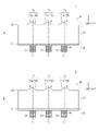
- FIG. 1 is a cross-sectional view showing an example of the structure of a light emitting device according to a first embodiment
- FIG. 3 is a cross-sectional view showing the structure of the light emitting device shown in FIG. 2B
- FIG. 1 is a cross-sectional view showing the structure of a light emitting device according to a first embodiment
- FIG. 1 is a plan view showing the structure of a light emitting device according to a first embodiment
- FIG. 4 is a cross-sectional view for explaining the operation of the light emitting device of the first embodiment
- FIG. It is a sectional view showing the structure of the light-emitting device of the modification of 1st Embodiment.
- FIG. 4 is a plan view showing the structure of a light emitting device of another modified example of the first embodiment;
- FIG. 4 is a cross-sectional view showing the structure of a light-emitting device of another modified example of the first embodiment;
- FIG. 4 is a cross-sectional view showing the structure of a light-emitting device of another modified example of the first embodiment;
- FIG. 4 is a plan view showing the structure of a light emitting device of another modified example of the first embodiment;
- FIG. 4 is a plan view showing the structure of a light emitting device of another modified example of the first embodiment;
- 8A and 8B are a plan view and a cross-sectional view showing the structure of a light-emitting device of another modified example of the first embodiment;
- FIG. 4 is a plan view showing the structure of a light emitting device of another modified example of the first embodiment;
- FIG. 4 is a cross-sectional view showing the structure of a light-emitting device of another modified example of the
- FIG. 8A and 8B are a plan view and a cross-sectional view showing the structure of a light-emitting device of another modified example of the first embodiment
- FIG. 4A to 4C are cross-sectional views showing a method for manufacturing the light emitting device of the first embodiment
- FIG. 11 is a cross-sectional view (1/2) showing a method of manufacturing a light emitting device according to a modification of the first embodiment
- It is a cross-sectional view (2/2) showing a method of manufacturing a light-emitting device of a modification of the first embodiment.
- FIG. 1 is a block diagram showing the configuration of the distance measuring device of the first embodiment.
- the distance measuring device in FIG. 1 includes a light emitting device 1, an imaging device 2, and a control device 3.
- the distance measuring device of FIG. 1 irradiates a subject with light emitted from a light emitting device 1 .
- the imaging device 2 captures an image of the subject by receiving light reflected by the subject.
- the control device 3 measures (calculates) the distance to the subject using the image signal output from the imaging device 2 .
- the light emitting device 1 functions as a light source for the imaging device 2 to capture an image of a subject.
- the light-emitting device 1 includes a light-emitting portion 11, a drive circuit 12, a power supply circuit 13, and a light-emitting side optical system .
- the imaging device 2 includes an image sensor 21 , an image processing section 22 and an imaging side optical system 23 .
- the control device 3 has a distance measuring section 31 .
- the light emitting unit 11 emits laser light for irradiating the subject.
- the light emitting section 11 of this embodiment includes a plurality of light emitting elements arranged in a two-dimensional array, and each light emitting element has a VCSEL structure. A subject is irradiated with light emitted from these light emitting elements.
- the light emitting section 11 of this embodiment is provided in a chip called an LD (Laser Diode) chip 41 .
- the drive circuit 12 is an electric circuit that drives the light emitting section 11
- the power circuit 13 is an electric circuit that generates a power supply voltage for the drive circuit 12 .
- the power supply circuit 13 generates a power supply voltage from the input voltage supplied from the battery in the rangefinder, and the drive circuit 12 drives the light emitting section 11 using this power supply voltage.
- the drive circuit 12 of this embodiment is provided in a substrate called an LDD (Laser Diode Driver) substrate 42 .
- the light-emitting side optical system 14 includes various optical elements, and irradiates the subject with light from the light-emitting section 11 via these optical elements.
- the imaging side optical system 23 includes various optical elements, and receives light from the subject via these optical elements.
- the image sensor 21 receives light from the subject via the imaging side optical system 23 and converts this light into an electrical signal by photoelectric conversion.
- the image sensor 21 is, for example, a CCD (Charge Coupled Device) sensor or a CMOS (Complementary Metal Oxide Semiconductor) sensor.
- the image sensor 21 of this embodiment converts the above electronic signal from an analog signal to a digital signal by A/D (Analog to Digital) conversion, and outputs an image signal as a digital signal to the image processing section 22 . Further, the image sensor 21 of the present embodiment outputs a frame synchronization signal to the driving circuit 12, and the driving circuit 12 causes the light emitting section 11 to emit light at a timing corresponding to the frame period of the image sensor 21 based on the frame synchronization signal.
- the image processing unit 22 performs various image processing on the image signal output from the image sensor 21 .
- the image processing unit 22 includes an image processing processor such as a DSP (Digital Signal Processor).
- DSP Digital Signal Processor
- the control device 3 controls various operations of the distance measuring device in FIG.
- the control device 3 includes, for example, a CPU (Central Processing Unit), ROM (Read Only Memory), RAM (Random Access Memory), and the like.
- the distance measuring unit 31 measures the distance to the subject based on the image signal output from the image sensor 21 and subjected to image processing by the image processing unit 22 .
- the distance measurement unit 31 employs, for example, the STL (Structured Light) method or the ToF (Time of Flight) method as a distance measurement method. Further, the distance measuring unit 31 may measure the distance between the distance measuring device and the subject for each part of the subject based on the above image signal, and specify the three-dimensional shape of the subject. Further details of the distance measuring unit 31 of the present embodiment will be described later.
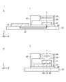
- FIG. 2 is a cross-sectional view showing an example of the structure of the light emitting device 1 of the first embodiment.
- FIG. 2A shows a first example of the structure of the light emitting device 1 of this embodiment.
- the light emitting device 1 of this example includes the above-described LD chip 41 and LDD substrate 42, a mounting substrate 43, a heat dissipation substrate 44, a correction lens holding portion 45, one or more correction lenses 46, and wiring 47. ing.
- a in FIG. 2 shows the X-axis, Y-axis, and Z-axis that are perpendicular to each other.
- the X and Y directions correspond to the lateral direction (horizontal direction), and the Z direction corresponds to the longitudinal direction (vertical direction).
- the +Z direction corresponds to the upward direction, and the -Z direction corresponds to the downward direction.
- the -Z direction may or may not exactly match the direction of gravity.
- the LD chip 41 is arranged on the mounting board 43 via the heat dissipation board 44 , and the LDD board 42 is also arranged on the mounting board 43 .
- the mounting substrate 43 is, for example, a printed circuit board.
- the image sensor 21 and the image processing unit 22 shown in FIG. 1 are also arranged on the mounting substrate 43 of the present embodiment.
- the heat dissipation substrate 44 is, for example, a ceramic substrate such as an aluminum oxide substrate or an aluminum nitride substrate.
- the correction lens holding part 45 is arranged on the heat dissipation substrate 44 so as to surround the LD chip 41 and holds one or more correction lenses 46 above the LD chip 41 .
- These correcting lenses 46 are included in the above-described light emitting side optical system 14 (FIG. 1).
- the light emitted from the light emitting section 11 (FIG. 1) in the LD chip 41 is corrected by these correcting lenses 46 and then irradiated onto the subject (FIG. 1).
- FIG. 2A shows, as an example, two correction lenses 46 held by the correction lens holding portion 45.
- the wiring 47 is provided on the front surface, back surface, inside, etc. of the mounting substrate 43 and electrically connects the LD chip 41 and the LDD substrate 42 .
- the wiring 47 is, for example, a printed wiring provided on the front surface or the rear surface of the mounting substrate 43 or a via wiring that penetrates the mounting substrate 43 .
- the wiring 47 of this embodiment also passes through or near the heat dissipation substrate 44 .
- FIG. 2B shows a second example of the structure of the light emitting device 1 of this embodiment.
- the light emitting device 1 of this example has the same components as the light emitting device 1 of the first example, but has bumps 48 instead of the wirings 47 .
- the LDD substrate 42 is arranged on the heat dissipation substrate 44, and the LD chip 41 is arranged on the LDD substrate 42.
- the LD chip 41 is placed on the LDD substrate 42 via the bumps 48 and electrically connected to the LDD substrate 42 by the bumps 48 .
- the light-emitting device 1 of this embodiment will be described below assuming that it has the structure of the second example shown in FIG. 2B. However, the following description is also applicable to the light emitting device 1 having the structure of the first example, except for the description of the structure specific to the second example.
- FIG. 3 is a cross-sectional view showing the structure of the light emitting device 1 shown in FIG. 2B.
- FIG. 3 shows a cross section of the LD chip 41 and the LDD substrate 42 in the light emitting device 1.
- the LD chip 41 includes a substrate 51, a laminated film 52, a plurality of light emitting elements 53, a plurality of anode electrodes 54, and a plurality of cathode electrodes 55.
- the LDD substrate 42 is , a substrate 61 and a plurality of connection pads 62 . 3, illustration of a structure 71, which will be described later, is omitted (see FIG. 4).
- the substrate 51 is a semiconductor substrate such as a GaAs (gallium arsenide) substrate.
- FIG. 3 shows the front surface S1 of the substrate 51 facing the ⁇ Z direction and the rear surface S2 of the substrate 51 facing the +Z direction.
- the front surface S1 is an example of the first surface of the present disclosure
- the back surface S2 is an example of the second surface of the present disclosure.
- the laminated film 52 includes multiple layers laminated on the surface S1 of the substrate 51 . Examples of these layers are an n-type semiconductor layer, an active layer, a p-type semiconductor layer, a light reflecting layer, an insulating layer with an exit window for light, and the like.
- the laminated film 52 includes a plurality of mesa portions M projecting in the -Z direction. A part of these mesa portions M are a plurality of light emitting elements 53 .
- the light emitting element 53 is provided on the surface S ⁇ b>1 of the substrate 51 as part of the laminated film 52 .
- the light emitting element 53 of this embodiment has a VCSEL structure and emits light in the +Z direction. As shown in FIG. 3, the light emitted from the light emitting element 53 passes through the substrate 51 from the surface S1 to the rear surface S2, and enters the correcting lens 46 (FIG. 2) from the substrate 51.
- the LD chip 41 of this embodiment is a back emission type VCSEL chip.
- the anode electrode 54 is formed on the bottom surface of the light emitting element 53 .
- the cathode electrode 55 is formed on the lower surface of the mesa portion M other than the light emitting element 53 and extends to the lower surface of the laminated film 52 between the mesa portions M. As shown in FIG. Each light emitting element 53 emits light when a current flows between the corresponding anode electrode 54 and the corresponding cathode electrode 55 .
- the LD chip 41 is arranged on the LDD substrate 42 via the bumps 48 and electrically connected to the LDD substrate 42 by the bumps 48 .
- a connection pad 62 is formed on a substrate 61 included in the LDD substrate 42
- a mesa portion M is arranged on the connection pad 62 via a bump 48 .
- Each mesa portion M is arranged on the bump 48 via the anode electrode 54 or the cathode electrode 55 .
- the substrate 61 is, for example, a semiconductor substrate such as a Si (silicon) substrate.
- the LDD board 42 includes a drive circuit 12 that drives the light emitting section 11 (Fig. 1).
- FIG. 3 schematically shows a plurality of switches SW included in the drive circuit 12. As shown in FIG. Each switch SW is electrically connected to the corresponding light emitting element 53 via the bump 48 .
- the drive circuit 12 of the present embodiment can control (turn on and off) these switches SW individually. Therefore, the driving circuit 12 can drive the plurality of light emitting elements 53 individually. This makes it possible to precisely control the light emitted from the light emitting section 11, for example, by causing only the light emitting element 53 required for distance measurement to emit light.
- Such individual control of the light emitting elements 53 can be realized by arranging the LDD substrate 42 below the LD chip 41, thereby making it easier to electrically connect each light emitting element 53 to the corresponding switch SW. ing.
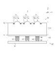
- FIG. 4 is a cross-sectional view showing the structure of the light emitting device 1 of the first embodiment.
- FIG. 4 shows a cross section of the LD chip 41 and the LDD substrate 42 in the light emitting device 1.
- the LD chip 41 includes the substrate 51, the laminated film 52, the plurality of light emitting elements 53, the plurality of anode electrodes 54, and the plurality of cathode electrodes 55.
- the LDD substrate 42 is a substrate 61 and a plurality of connection pads 62 .
- illustration of the anode electrode 54, the cathode electrode 55, and the connection pad 62 is omitted.
- the LD chip 41 of this embodiment includes a plurality of light emitting elements 53 on the front surface S1 of the substrate 51 and a plurality of structural bodies 71 on the rear surface S2 of the substrate 51 . These structures 71 are arranged in a two-dimensional array like the light emitting elements 53 .
- the structures 71 of this embodiment correspond to the light emitting elements 53 on a one-to-one basis, and each structure 71 is arranged in the +Z direction of one light emitting element 53 .
- Each structure 71 includes a first structure 71a and a second structure 71b.
- the first structure 71a is, for example, a lens.
- the first structure 71a of the present embodiment is a convex lens having a convex upper surface, and can focus light.
- the first structure 71a may be a lens other than a convex lens, such as a concave lens or a flat lens.
- the second structure 71b is, for example, a structure other than a lens.
- the second structure 71b of the present embodiment is a scatterer including a plurality of fine dot-shaped projections, and can scatter light.
- the second structure 71b may be a structure other than the scatterer, and may be, for example, a lens having a function different from that of the lens of the first structure 71a.
- the first structure 71a and the second structure 71b of this embodiment have a shape in which the second structure 71b surrounds the first structure 71a in an annular shape (see FIG. 5).
- the shape of the first structure 71a in plan view is circular, and the shape of the second structure 71b in plan view is annular.
- the structure 71 of the present embodiment is provided on the rear surface S2 of the substrate 51 as part of the substrate 51 .
- the structure 71 of this embodiment is formed by processing the substrate 51 from the back surface S2. According to this embodiment, the structure 71 can be easily formed by processing the substrate 51 .
- the structure 71 may be formed on a film provided on the substrate 51 instead of forming it on the substrate 51 .
- the light emitting element 53 on the substrate 51 (GaAs substrate) that is suitable for improving the performance of the light emitting element 53 while suppressing damage to the substrate 51 due to the processing of the substrate 51 .
- the structure 71 on the substrate 51, the light emitting device 1 can be manufactured while forming the light emitting element 53 on the substrate 51 (GaAs substrate) suitable for improving the performance of the light emitting element 53. Miniaturization is possible.
- the light emitted from the plurality of light emitting elements 53 passes through the substrate 51 from the front surface S1 to the back surface S2 and enters the structure 71 .
- the light emitted from each light emitting element 53 enters one corresponding structure 71 .
- the light incident on each structure 71 is emitted from the substrate 51 by passing through each structure 71, and enters the correction lens 46 (FIG. 2) described above.
- the light that has passed through the correction lens 46 is applied to the subject (FIG. 1).
- each light emitting element 52 When light emitted from each light emitting element 52 is incident on one corresponding structure 71, this light is incident on a first structure 71a and a second structure 71b of this structure 71, as will be described later. (see Figure 6). Specifically, a first portion of this light enters the first structure 71a and a second portion of this light enters the second structure 72b. In this embodiment, the central portion and the peripheral portion of the light incident on each structure 71 are the first portion and the second portion, respectively. The first portion passes through the first structure 71b and enters the correction lens 46, and the second portion passes through the second structure 71b and enters the correction lens 46.
- the light-emitting device 1 of the present embodiment includes the structures 71 that shape the light emitted from the light-emitting elements 53, and each structure 71 is a first structure that shapes the first portion of the light. It includes a structure 71a and a second structure 71b that shapes a second portion of this light. Therefore, according to the present embodiment, the light from the light emitting element 53 is suitable because the light incident on the structure 71 from the light emitting element 53 can be shaped differently between the first structure 71a and the second structure 71b. It becomes possible to mold to
- a lens such as the first structure 71a is arranged above a certain light emitting element 53 and a scatterer such as the second structure 71b is arranged above another light emitting element 53, then converged light and scattered light can generate both In this case, the light-emitting element 53 below the scatterer is unnecessary when generating focused light. On the other hand, when generating scattered light, the light emitting element 53 below the lens is unnecessary. As a result, the unused light emitting elements 53 are wasted.
- each light emitting element 53 of this embodiment is used when generating either converged light or scattered light. Therefore, according to the present embodiment, each structural body 71 includes the first structural body 71a and the second structural body 71b, so that the waste of the light emitting elements 53 can be reduced. In other words, according to this embodiment, it is possible to make the distance measuring device multi-functional with a small number of light emitting elements 53, and realize low power consumption, size reduction, weight reduction, and high accuracy of the distance measuring device. becomes possible.
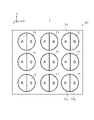
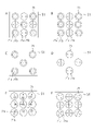
- FIG. 5 is a plan view showing the structure of the light emitting device 1 of the first embodiment.
- FIG. 5 shows a region A of a first structure 71a within each structure 71 and a region B of a second structure 71b within each structure 71.
- FIG. 5 shows a region A of a first structure 71a within each structure 71 and a region B of a second structure 71b within each structure 71.
- the shape of the area A is circular
- the shape of the area B is an annular ring surrounding the area A.
- the second structure 71b surrounds the first structure 71a in a ring shape.
- the number of structural bodies 71 on the back surface S2 of the substrate 51 may be other than nine, and the arrangement of these structural bodies 71 may be other than the arrangement shown in FIG.
- an example of the first structure 71a is a lens
- an example of the second structure 71b is a scatterer. It is often desirable that the planar shape of the lens be circular. According to this embodiment, by using the first structure 71a as a lens, it is possible to make the planar shape of the lens circular. On the other hand, the planar shape of the scatterer does not have to be circular in many cases. Therefore, the second structure 71b of this embodiment is a scatterer, and the planar shape of this scatterer is non-circular.
- the second structural body 71b of the present embodiment includes a plurality of protrusions that are regularly arranged two-dimensionally (FIG. 4). may contain.
- FIG. 6 is a cross-sectional view for explaining the operation of the light emitting device 1 of the first embodiment.
- FIG. 6A shows a first portion La of the light emitted from the light emitting element 53 that passes through the first structure 71a.
- B of FIG. 6 shows a second portion Lb of the light emitted from the light emitting element 53 that passes through the second structure 71b.
- FIG. 6C collectively shows the first portion La and the second portion Lb.
- the light emitted from each light emitting element 53 enters the corresponding structure 71 as shown in FIG. 6C.
- This light includes a first portion La that enters the first structure 71a and a second portion Lb that enters the second structure 71b.
- the first structure 71a is, for example, a convex lens, and has a function of converging incident light.
- the second structure 71b is, for example, a scatterer and has a function of scattering incident light. Therefore, the first portion La transmitted through the first structure 71a becomes converged light as shown in FIG. 6A, and the second portion Lb transmitted through the second structure 71b becomes converged light as shown in FIG. 6B. It becomes scattered light.
- the structure 71 emits converged light (first portion La) and scattered light (second portion Lb) at the same time.
- the first structure 71a of the present embodiment collimates the first portion La by converging the first portion La. Therefore, the first portion La that has passed through the first structure 71a of the present embodiment becomes parallel light.
- the distance measurement unit 31 measures the distance to the subject based on the image signal generated by the imaging device 2.
- the image signal of this embodiment includes first data corresponding to the first portion La transmitted through the first structure 71a of each structure 71 and second portion Lb transmitted through the second structure 71b of each structure 71. and second data corresponding to . Therefore, the distance measuring unit 31 performs information processing to extract the first data and the second data from the image signal, and measures the distance to the subject using the extracted first data and the extracted second data. do.
- the distance measuring unit 31 may measure the distance to a certain part of the subject using the first data, and measure the distance to another part of the subject using the second data. Further, the distance measuring section 31 may measure the distance to the subject by combining a first process using the first data and a second process using the second data.
- the first data and the second data may be extracted from the image signal in any manner.
- the distance measurement unit 13 includes a separation unit that separates the image signal into a focused light component and a scattered light component, a first calculation unit that extracts first data from the focused light component, and a second data from the scattered light component. and a second calculation unit for extracting.
- the distance measurement section 13 may measure the distance to the subject based on the first data extracted by the first calculation section and the second data extracted by the second calculation section.
- the distance measurement unit 13 includes a first output unit that outputs the first data extracted by the first calculation unit to the outside, and a second output unit that outputs the second data extracted by the second calculation unit to the outside. and may be provided. Also, such first and second output units may be provided outside the distance measuring unit 13 or outside the control device 3 .
- FIGS. 7 to 14 are sectional views and plan views showing structures of light-emitting devices 1 of various modifications of the first embodiment.
- each first structure 71a is a concave lens having a concave upper surface, and can diffuse light.
- the first structure 71a of the present embodiment may be any type of lens in accordance with the purpose of using light.
- the light-emitting device 1 shown in FIG. 7B includes various types of lenses as the first structure 71a.
- FIG. 7B shows a convex lens having a convex upper surface, a concave lens having a concave upper surface, and a flat lens having a flat upper surface as examples of the first structure 71a.
- the state in which the flat lens exists above the light emitting element 53 can also be said to be the state in which the lens does not exist above the light emitting element 53 .
- the light-emitting device 1 of this embodiment may include two or more types of lenses as the first structure 71a.
- the light emitting device 1 shown in FIG. 8 is a modification of the light emitting device 1 shown in FIG.
- the area A of the first structure 71a is circular, and the area B of the second structure 71b is annular.
- the region A of the first structure 71a is semicircular, and the region B of the second structure 71b is also semicircular. Therefore, the boundary surface between the regions A and B shown in FIG. 5 has a cylindrical shape extending in the Z direction, whereas the boundary surface between the regions A and B shown in FIG. 8 extends in the Z direction. It is flat.
- the boundary plane is the YZ plane.
- each structural body 71 can be divided into two on a plane to set the area A and the area B, so that the first structural body 71a and the second structural body 71b can be arranged in a simple layout. becomes possible.
- the area of the region A and the area of the region B may be the same or different.
- structures shown in FIGS. 9A to 10B will be described as specific examples of this modification.
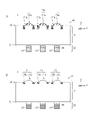
- a of FIG. 9 shows a plane C (YZ plane) passing through the center of each light emitting element 53 .
- Each structure 71 of this modification includes a first structure 71a that is a convex lens and a second structure 71b that is a convex lens having a function different from that of the convex lens of the first structure 71a. It is a boundary surface between the first structure 71a and the second structure 71b.
- the first structure 71a and the second structure 71b of this modified example are convex lenses having curvatures different from each other. 71b has a small radius of curvature. Therefore, the first structural body 71a and the second structural body 71b of this modified example can focus light in mutually different manners.
- Each structure 71 shown in FIG. 9B also includes a first structure 71a that is a convex lens and a second structure 71b that is a convex lens.
- a first structure 71a that is a convex lens
- a second structure 71b that is a convex lens.
- the radius of curvature of the first structure 71a is larger than the radius of curvature of the second structure 71b
- the radius of curvature of the first structure 71a It also includes structure 71 with a smaller radius of curvature than 71b. Accordingly, like the light emitting device 1 shown in FIG. 7B, it is possible to shape light in various modes for each light emitting element 53 (for each structure 71).
- the light-emitting device 1 shown in FIG. 9B includes not only the structure 71 in which the functions of the first structure 71a and the second structure 71b are different, but also the functions of the first structure 71a and the second structure 71b. also includes the same structure 71 as an exception.
- the central structure 71 shown in FIG. 9B includes a first structure 71a and a second structure 71b having the same size and the same radius of curvature. and the second structure 71b can focus the light to the same extent.
- the structures 71 other than the central structure 71 can exhibit the function of shaping light in different modes between the first structure 71a and the second structure 71b. This also applies to the light emitting device 1 shown in A of FIG. 10, which will be described later.
- FIG. 10A shows a plane C (YZ plane) passing through the center of each light emitting element 53 and a plane C' (YZ plane) parallel to the plane C.
- FIG. Each structure 71 of this modified example has the same shape as each structure 71 shown in FIG. 71b.
- the plane C' is positioned on the right side of the plane C
- the plane C' is positioned on the left side of the plane C. there is This makes it possible to apply pupil correction to the light emitted from these structures 71 .
- Each structure 71 shown in FIG. 10B includes a first structure 71a that is a lens and a second structure 71b that is a structure other than the lens.
- the first structure 71a is, for example, a convex lens.
- the second structure 71b is, for example, a scatterer.
- Each structural body 71 of this modified example has a shape obtained by modifying the shape of the regions A and B of each structural body 71 shown in FIG.
- 11A to 11F are plan views schematically showing the structure of the light emitting device 1 of another modified example of the present embodiment.
- symbol ⁇ indicates the region where the first type structure 71 is arranged on the back surface S2 of the substrate 51, and symbol ⁇ indicates the second structure on the back surface S2 of the substrate 51.
- the symbol ⁇ indicates the region where the structure 71 of the third type is arranged on the back surface S2 of the substrate 51, and the symbol ⁇ indicates the back surface of the substrate 51.
- S2 indicates a region where the fourth type structure 71 is arranged.
- the first type structure 71 includes, for example, a first structure 71a that is a convex lens and a second structure 71b that is a scatterer.
- the second type structure 71 includes, for example, a first structure 71a that is a concave lens and a second structure 71b that is a scatterer.
- the third type structure 71 includes, for example, a first structure 71a that is a flat lens and a second structure 71b that is a scatterer.
- the fourth type of structure 71 includes, for example, a first structure 71a and a second structure 71b that are convex lenses having curvatures different from each other.
- these regions are referred to as " ⁇ region", “ ⁇ region”, “ ⁇ region”, and " ⁇ region”.
- the rear surface S2 of the substrate 51 is divided into two regions, one region being the ⁇ region and the other region being the ⁇ region.
- the ⁇ region includes (N/2) ⁇ M structures 71
- the ⁇ region includes (N/2) It contains xM structures 71 (N and M are integers of 2 or more).
- the back surface S2 of the substrate 51 is divided into two regions.
- the rear surface S2 of the substrate 51 is divided into three regions, and these regions are ⁇ region, ⁇ region, and ⁇ region.
- the ⁇ region includes (N/3) ⁇ M structures 71
- the ⁇ region includes (N/3) xM structures 71 are included
- the ⁇ region includes (N/3) ⁇ M structures 71 .
- the rear surface S2 of the substrate 51 is divided into three regions.
- the rear surface S2 of the substrate 51 is divided into four regions, and these regions are ⁇ region, ⁇ region, ⁇ region, and ⁇ region.
- the ⁇ region includes (N/2) ⁇ (M/2) structures 71, and the ⁇ region ( N/2) ⁇ (M/2) structures 71 are included, the ⁇ region includes (N/2) ⁇ (M/2) structures 71, and the ⁇ region is (N/2) ⁇ ( M/2) structures 71 are included.
- FIGS. 12A to 12F are plan views schematically showing the structure of the light-emitting device 1 of another modified example of the present embodiment.
- the rear surface S2 of the substrate 51 is divided into several regions, whereas in FIGS. 12A to 12F, the rear surface S2 of the substrate 51 is subdivided into a large number of regions. .
- FIG. 12A shows nine structures 71 provided on the back surface S2 of the substrate 51.
- FIG. These structures 71 include a structure 71 including regions A and B shaped as shown in FIG. 5 and a structure 71 including regions A and B shaped as shown in FIG. This also applies to B in FIG. 12A and 12B, however, the layout of the structure 71 having the shape shown in FIG. 5 and the structure 71 having the shape shown in FIG. 8 are different.
- a structure 71 shown in FIG. 12C includes a structure 71 including regions A and B shaped as shown in FIG. However, the rear surface S2 of the substrate 51 shown in FIG. 12C includes a region where the structural bodies 71 are arranged and a region where the structural bodies 71 are not arranged. This also applies to D in FIG.
- a structure 71 shown in FIG. 12D includes a structure 71 including regions A and B shaped as shown in FIG. However, the rear surface S2 of the substrate 51 shown in FIG. 12D includes an area where the structural bodies 71 are arranged and an area where the structural bodies 71 are not arranged. Note that the layout of these structures 71 is different between C of FIG. 12 and FIG. 12D.
- FIG. 12E shows nine structures 71 provided on the rear surface S2 of the substrate 51.
- FIG. Reference P indicates the center of the substrate 51 .
- a structure 71 shown in E of FIG. 12 includes a structure 71 including regions A and B having the shapes shown in FIG. This also applies to F in FIG.
- a structure 71 shown in FIG. 12F includes structures 71 including regions A and B having the shape shown in FIG. 8, and pupil correction can be applied to light emitted from these structures 71.
- pupil correction is realized by changing the position of the region A with respect to the region B for each structure 71 .
- FIG. 12F pupil correction is realized by changing the direction of the boundary surface between the regions A and B for each structure 71 .
- FIG. 13A to 13C are a plan view and a cross-sectional view showing the structure of the light emitting device 1 of another modified example of this embodiment.
- a of FIG. 13 shows a planar shape of one structure 71 .
- B of FIG. 13 shows the light (first portion La) transmitted through the first structure 71a of this structure 71.
- FIG. C of FIG. 13 shows the light (second portion Lb) that has passed through the second structure 71b of this structure 71 .
- the structures shown in FIGS. 13A to 13C can be adopted, for example, when it is desired to enhance the effect of the second structure 71b (eg, scatterer).
- the structures shown in FIGS. 14A to 14C can be adopted, for example, when the effect of the first structure 71a (for example, lens) is desired to be enhanced.
- the shapes of the regions A and B it is possible to adjust the function of the structure 71 .
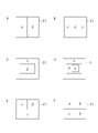
- FIG. 15 is a cross-sectional view showing a method for manufacturing the light-emitting device 1 of the first embodiment.
- the mask film 72 is formed on the rear surface S2 of the substrate 51 (A in FIG. 15).
- the mask film 72 is, for example, a resist film.
- each mask portion 73 is formed to include a first mask portion 73a having the same shape as the first structure 71a and a second mask portion 73b having the same shape as the second structure 71b.
- the processing of the upper surface of the mask film 72 may be performed, for example, by grayscale lithography and dry etching, or may be performed by imprinting.
- a first mask portion 73a and a second mask portion 73b shown in FIG. 15B have the shapes of a convex lens and a scatterer, respectively.
- each structure 71 is formed to include a first structure 71a and a second structure 71b.
- the light emitting device 1 shown in FIG. 4 is manufactured.
- the first structure 71a and the second structure 71b of each structure 71 can be formed on the rear surface S2 of the substrate 51 at the same time.
- a mask portion 72 having the same shape as the structural body 71 of the modification is formed in the step of B in FIG.
- FIGS. 16 and 17 are cross-sectional views showing a manufacturing method of the light-emitting device 1 of a modification of the first embodiment.
- each structure 71 is formed on the back surface S2 of the substrate 51 (A in FIG. 16).
- the second structure 71b can be formed, for example, by the steps shown in FIGS. 15A to 15C.
- each mask portion 73 is formed so as not to include the first mask portion 73a but to include the second mask portion 73b.
- the second structure 71b shown in A of FIG. 16 is a scatterer. However, the height of each protrusion of the second structure 71b shown in A of FIG. 16 is set to the height of each protrusion shown in FIG. is higher than the height of
- a mask film 74 is formed on the back surface S2 of the substrate 51 (B in FIG. 16).
- the mask film 74 is, for example, a resist film.
- the mask film 74 is processed into a shape including a mask portion 74a having the same shape as the first structure 71a of each structure 71 (A in FIG. 17).
- the processing of the mask film 74 may be performed, for example, by grayscale lithography and dry etching, or may be performed by imprinting.
- Each mask portion 74a shown in FIG. 17A has a convex lens shape and is formed at a position surrounded by the corresponding second structure 71b.
- each structure 71 is processed into a shape including a first structure 71a and a second structure 71b.
- the light emitting device 1 shown in FIG. 4 is manufactured.
- the first structure 71a of each structure 71 can be formed on the back surface S2 of the substrate 51 after the second structure 71b of each structure 71 is formed on the back surface S2 of the substrate 51.
- the first structure 71a and the second structure 71b of each structure 71 can be formed on the rear surface S2 of the substrate 51 in order.
- the second structure 71b of each structure 71 may be formed on the back surface S2 of the substrate 51 after the first structure 71a of each structure 71 is formed on the back surface S2 of the substrate 51 .
- the mask portion 73 (second mask portion 73b) for forming the second structure 71b of the modification and the mask portion 73b of the modification
- a mask portion 74a for forming the first structure 71a is formed in the steps of A of FIG. 16 and A of FIG.
- the structure 71 can be formed in a small number of steps.
- the structure 71 can be precisely formed.
- the light-emitting device 1 of the present embodiment includes a plurality of structures 71 that shape the light from the plurality of light-emitting elements 53, and at least one of these structures 71 is a primary component of this light. It includes a first structure 71a through which a portion La is transmitted, and a second structure 71b having a function different from that of the first structure 71a and through which a second portion Lb of this light is transmitted. Therefore, according to the present embodiment, the light from the light emitting element 53 is suitable because the light incident on the structure 71 from the light emitting element 53 can be shaped differently between the first structure 71a and the second structure 71b. It becomes possible to mold to
- the light emitting device 1 of this embodiment is used as the light source of the distance measuring device, it may be used in other ways.
- the light-emitting device 1 of this embodiment may be used as a light source for an optical device such as a printer, or may be used as a lighting device.
- a substrate a plurality of light emitting elements provided on the first surface of the substrate; a plurality of structures provided on the second surface of the substrate and through which light emitted from the plurality of light emitting elements is transmitted;
- Each of the structures includes a first structure that transmits a first portion of the light and a second structure that has a shape different from that of the first structure and transmits a second portion of the light. , luminous device.
- the substrate is a semiconductor substrate containing gallium (Ga) and arsenic (As).
- a method of manufacturing a light-emitting device comprising:
- first and second structures are formed by forming one of the first and second structures followed by forming the other of the first and second structures.
- a light-emitting device that includes a plurality of light-emitting elements that generate light and irradiates a subject with the light from the light-emitting elements; an imaging device that receives the light reflected by the subject and generates an image signal from the light; a distance measuring unit that measures the distance to the subject based on the image signal generated by the imaging device;
- the light emitting device a substrate; the plurality of light emitting elements provided on the first surface of the substrate; a plurality of structures provided on the second surface of the substrate and through which light emitted from the plurality of light emitting elements is transmitted; Each of the structures includes a first structure that transmits a first portion of the light and a second structure that has a shape different from that of the first structure and transmits a second portion of the light. , ranging device.
- the distance measuring unit converts the image signal into first data corresponding to the first portion of the light transmitted through the first structure and the second portion of the light transmitted through the second structure.
- the range finder according to (19), which extracts the corresponding second data.
Landscapes
- Physics & Mathematics (AREA)
- General Physics & Mathematics (AREA)
- Optics & Photonics (AREA)
- Engineering & Computer Science (AREA)
- Electromagnetism (AREA)
- Condensed Matter Physics & Semiconductors (AREA)
- Remote Sensing (AREA)
- Radar, Positioning & Navigation (AREA)
- Computer Networks & Wireless Communication (AREA)
- Signal Processing (AREA)
- Multimedia (AREA)
- Computer Vision & Pattern Recognition (AREA)
- Optical Radar Systems And Details Thereof (AREA)
- Measurement Of Optical Distance (AREA)
- Focusing (AREA)
- Optical Elements Other Than Lenses (AREA)
- Lens Barrels (AREA)
- Automatic Focus Adjustment (AREA)
- Studio Devices (AREA)
Abstract
Description
図1は、第1実施形態の測距装置の構成を示すブロック図である。
図2は、第1実施形態の発光装置1の構造の例を示す断面図である。
図7~図14は、第1実施形態の種々の変形例の発光装置1の構造を示す断面図と平面図である。
図12のEは、基板51の裏面S2に設けられた9個の構造体71を示している。符号Pは、基板51の中心を示している。図12のEに示す構造体71は、図5に示す形状の領域A、Bを含む構造体71を含んでおり、これらの構造体71から出射される光に瞳補正を施すことができる。これは、図12のFでも同様である。図12のFに示す構造体71は、図8に示す形状の領域A、Bを含む構造体71を含んでおり、これらの構造体71から出射される光に瞳補正を施すことができる。なお、図12のEでは、領域Bに対する領域Aの位置を各構造体71ごとに変えることで、瞳補正を実現している。一方、図12のFでは、領域Aと領域Bとの境界面の向きを各構造体71ごとに変えることで、瞳補正を実現している。
図15は、第1実施形態の発光装置1の製造方法を示す断面図である。
図16および図17は、第1実施形態の変形例の発光装置1の製造方法を示す断面図である。
基板と、
前記基板の第1面に設けられた複数の発光素子と、
前記基板の第2面に設けられ、前記複数の発光素子から出射された光が透過する複数の構造体とを備え、
前記構造体の各々は、前記光の第1部分が透過する第1構造体と、前記第1構造体と異なる形状を有し、前記光の第2部分が透過する第2構造体とを含む、発光装置。
前記第1および第2構造体は、前記第2構造体が前記第1構造体を環状に包囲する形状を有している、(1)に記載の発光装置。
前記第1および第2構造体の境界面は、平面である、(1)に記載の発光装置。
前記第1構造体はレンズであり、前記第2構造体はレンズ以外の構造体である、(1)に記載の発光装置。
前記第1構造体はレンズであり、前記第2構造体は散乱体である、(4)に記載の発光装置。
前記第1および第2構造体は、互いに異なる形状を有するレンズである、(1)に記載の発光装置。
前記第1および第2構造体は、互いに異なる曲率を有するレンズである、(6)に記載の発光装置。
前記第1および第2構造体の少なくともいずれかは、凸レンズ、凹レンズ、またはフラットレンズである、(1)に記載の発光装置。
前記第1および第2構造体は、前記基板の前記第2面に、前記基板の一部として設けられている、(1)に記載の発光装置。
前記複数の発光素子と前記複数の構造体は、1対1で対応しており、各発光素子から出射された光は、対応する1つの構造体を透過する、(1)に記載の発光装置。
前記基板は、ガリウム(Ga)およびヒ素(As)を含む半導体基板である、(1)に記載の発光装置。
前記複数の発光素子から出射された光は、前記基板内を前記第1面から前記第2面へと透過し、前記複数の構造体に入射する、(1)に記載の発光装置。
前記基板の前記第1面は、前記基板の表面であり、前記基板の前記第2面は、前記基板の裏面である、(1)に記載の発光装置。
前記第1構造体は、前記発光素子からの光を集束または拡散させ、前記第2構造体は、前記発光素子からの光を散乱させる、(1)に記載の発光装置。
前記第1構造体は、前記発光素子からの光をコリメートする、(14)に記載の発光装置。
基板の第1面に複数の発光素子を形成し、
前記基板の第2面に、前記複数の発光素子から出射された光が透過する複数の構造体を形成する、
ことを含み、
前記構造体の各々は、前記光の第1部分が透過する第1構造体と、前記第1構造体と異なる形状を有し、前記光の第2部分が透過する第2構造体とを含むように形成される、発光装置の製造方法。
前記第1および第2構造体は、前記基板の前記第2面に同時に形成される、(16)に記載の発光装置の製造方法。
前記第1および第2構造体は、前記第1および第2構造体の一方を形成した後に、前記第1および第2構造体の他方を形成することで形成される、(16)に記載の発光装置の製造方法。
光を発生させる複数の発光素子を含み、前記発光素子からの前記光を被写体に照射する発光装置と、
前記被写体で反射した前記光を受光して、前記光から画像信号を生成する撮像装置と、
前記撮像装置により生成された前記画像信号に基づいて、前記被写体までの距離を測定する測距部とを備え、
前記発光装置は、
基板と、
前記基板の第1面に設けられた前記複数の発光素子と、
前記基板の第2面に設けられ、前記複数の発光素子から出射された光が透過する複数の構造体とを備え、
前記構造体の各々は、前記光の第1部分が透過する第1構造体と、前記第1構造体と異なる形状を有し、前記光の第2部分が透過する第2構造体とを含む、測距装置。
前記測距部は、前記画像信号から、前記第1構造体を透過した前記光の前記第1部分に対応する第1データと、前記第2構造体を透過した前記光の前記第2部分に対応する第2データとを抽出する、(19)に記載の測距装置。
11:発光部、12:駆動回路、13:電源回路、14:発光側光学系、
21:イメージセンサ、22:画像処理部、23:撮像側光学系、31:測距部、
41:LDチップ、42:LDD基板、43:実装基板、44:放熱基板、
45:補正レンズ保持部、46:補正レンズ、47:配線、48:バンプ、
51:基板、52:積層膜、53:発光素子、54:アノード電極、
55:カソード電極、61:基板、62:接続パッド、
71:構造体、71a:第1構造体、71b:第2構造体、72:マスク膜、
73:マスク部分、73a:第1マスク部分、73b:第2マスク部分、
74:マスク膜、74a:マスク部分
Claims (20)
- 基板と、
前記基板の第1面に設けられた複数の発光素子と、
前記基板の第2面に設けられ、前記複数の発光素子から出射された光が透過する複数の構造体とを備え、
前記構造体の少なくともいずれかは、前記光の第1部分が透過する第1構造体と、前記第1構造体と異なる機能を有し、前記光の第2部分が透過する第2構造体とを含む、発光装置。 - 前記第1および第2構造体は、前記第2構造体が前記第1構造体を環状に包囲する形状を有している、請求項1に記載の発光装置。
- 前記第1および第2構造体の境界面は、平面である、請求項1に記載の発光装置。
- 前記第1構造体はレンズであり、前記第2構造体はレンズ以外の構造体である、請求項1に記載の発光装置。
- 前記第1構造体はレンズであり、前記第2構造体は散乱体である、請求項4に記載の発光装置。
- 前記第1および第2構造体は、互いに異なる機能を有するレンズである、請求項1に記載の発光装置。
- 前記第1および第2構造体は、互いに異なる曲率を有するレンズである、請求項6に記載の発光装置。
- 前記第1および第2構造体の少なくともいずれかは、凸レンズ、凹レンズ、またはフラットレンズである、請求項1に記載の発光装置。
- 前記第1および第2構造体は、前記基板の前記第2面に、前記基板の一部として設けられている、請求項1に記載の発光装置。
- 前記複数の発光素子と前記複数の構造体は、1対1で対応しており、各発光素子から出射された光は、対応する1つの構造体を透過する、請求項1に記載の発光装置。
- 前記基板は、ガリウム(Ga)およびヒ素(As)を含む半導体基板である、請求項1に記載の発光装置。
- 前記複数の発光素子から出射された光は、前記基板内を前記第1面から前記第2面へと透過し、前記複数の構造体に入射する、請求項1に記載の発光装置。
- 前記基板の前記第1面は、前記基板の表面であり、前記基板の前記第2面は、前記基板の裏面である、請求項1に記載の発光装置。
- 前記第1構造体は、前記発光素子からの光を集束または拡散させ、前記第2構造体は、前記発光素子からの光を散乱させる、請求項1に記載の発光装置。
- 前記第1構造体は、前記発光素子からの光をコリメートする、請求項14に記載の発光装置。
- 基板の第1面に複数の発光素子を形成し、
前記基板の第2面に、前記複数の発光素子から出射された光が透過する複数の構造体を形成する、
ことを含み、
前記構造体の少なくともいずれかは、前記光の第1部分が透過する第1構造体と、前記第1構造体と異なる機能を有し、前記光の第2部分が透過する第2構造体とを含むように形成される、発光装置の製造方法。 - 前記第1および第2構造体は、前記基板の前記第2面に同時に形成される、請求項16に記載の発光装置の製造方法。
- 前記第1および第2構造体は、前記第1および第2構造体の一方を形成した後に、前記第1および第2構造体の他方を形成することで形成される、請求項16に記載の発光装置の製造方法。
- 光を発生させる複数の発光素子を含み、前記発光素子からの前記光を被写体に照射する発光装置と、
前記被写体で反射した前記光を受光して、前記光から画像信号を生成する撮像装置と、
前記撮像装置により生成された前記画像信号に基づいて、前記被写体までの距離を測定する測距部とを備え、
前記発光装置は、
基板と、
前記基板の第1面に設けられた前記複数の発光素子と、
前記基板の第2面に設けられ、前記複数の発光素子から出射された光が透過する複数の構造体とを備え、
前記構造体の少なくともいずれかは、前記光の第1部分が透過する第1構造体と、前記第1構造体と異なる機能を有し、前記光の第2部分が透過する第2構造体とを含む、測距装置。 - 前記測距部は、前記画像信号から、前記第1構造体を透過した前記光の前記第1部分に対応する第1データと、前記第2構造体を透過した前記光の前記第2部分に対応する第2データとを抽出する、請求項19に記載の測距装置。
Priority Applications (1)
| Application Number | Priority Date | Filing Date | Title |
|---|---|---|---|
| US18/261,725 US20250079801A1 (en) | 2021-01-26 | 2022-01-12 | Light emitting device, manufacturing method for light emitting device, and distance measuring device |
Applications Claiming Priority (2)
| Application Number | Priority Date | Filing Date | Title |
|---|---|---|---|
| JP2021-010424 | 2021-01-26 | ||
| JP2021010424A JP2022114220A (ja) | 2021-01-26 | 2021-01-26 | 発光装置、発光装置の製造方法、および測距装置 |
Publications (1)
| Publication Number | Publication Date |
|---|---|
| WO2022163353A1 true WO2022163353A1 (ja) | 2022-08-04 |
Family
ID=82653330
Family Applications (1)
| Application Number | Title | Priority Date | Filing Date |
|---|---|---|---|
| PCT/JP2022/000729 Ceased WO2022163353A1 (ja) | 2021-01-26 | 2022-01-12 | 発光装置、発光装置の製造方法、および測距装置 |
Country Status (3)
| Country | Link |
|---|---|
| US (1) | US20250079801A1 (ja) |
| JP (1) | JP2022114220A (ja) |
| WO (1) | WO2022163353A1 (ja) |
Cited By (1)
| Publication number | Priority date | Publication date | Assignee | Title |
|---|---|---|---|---|
| US20240276859A1 (en) * | 2023-02-15 | 2024-08-15 | Japan Display Inc. | Manufacturing method of display device |
Families Citing this family (1)
| Publication number | Priority date | Publication date | Assignee | Title |
|---|---|---|---|---|
| JP2023037044A (ja) * | 2020-02-19 | 2023-03-15 | ソニーセミコンダクタソリューションズ株式会社 | 発光装置およびその製造方法 |
Citations (10)
| Publication number | Priority date | Publication date | Assignee | Title |
|---|---|---|---|---|
| JPH08262204A (ja) * | 1995-03-20 | 1996-10-11 | Nikon Corp | 一体成形レンズ |
| US20140071431A1 (en) * | 2012-09-07 | 2014-03-13 | Apple Inc. | Imaging range finding device and method |
| WO2015122300A1 (ja) * | 2014-02-13 | 2015-08-20 | ソニー株式会社 | 撮像素子、製造装置、電子機器 |
| WO2016042642A1 (ja) * | 2014-09-18 | 2016-03-24 | 富士通フロンテック株式会社 | 測距光生成装置 |
| JP2017162394A (ja) * | 2016-03-11 | 2017-09-14 | 富士通株式会社 | 生体撮影装置、生体撮影方法および生体撮影プログラム |
| JP2018004464A (ja) * | 2016-07-04 | 2018-01-11 | オムロンオートモーティブエレクトロニクス株式会社 | 車両用光学式レーダ装置 |
| WO2019017044A1 (ja) * | 2017-07-18 | 2019-01-24 | ソニー株式会社 | 発光素子及び発光素子アレイ |
| JP2020153820A (ja) * | 2019-03-20 | 2020-09-24 | 株式会社リコー | 光学装置、検出装置及び電子機器 |
| JP2020181186A (ja) * | 2019-04-25 | 2020-11-05 | キヤノン株式会社 | 撮像装置及びその制御方法 |
| WO2021235162A1 (ja) * | 2020-05-22 | 2021-11-25 | ソニーセミコンダクタソリューションズ株式会社 | 発光装置および測距装置 |
Family Cites Families (7)
| Publication number | Priority date | Publication date | Assignee | Title |
|---|---|---|---|---|
| JPS60103310A (ja) * | 1983-11-11 | 1985-06-07 | Pioneer Electronic Corp | マイクロフレネルレンズの製造方法 |
| GB2434914A (en) * | 2006-02-03 | 2007-08-08 | Univ College Cork Nat Univ Ie | Vertical cavity surface emitting laser device |
| EP3382828A1 (en) * | 2017-03-31 | 2018-10-03 | Koninklijke Philips N.V. | Inherently safe laser arrangement comprising a vertical cavity surface emitting laser |
| US10895642B2 (en) * | 2017-10-18 | 2021-01-19 | Tdk Taiwan Corp. | Distance measuring device |
| CN108490637B (zh) * | 2018-04-03 | 2019-08-23 | Oppo广东移动通信有限公司 | 激光发射器、光电设备、深度相机和电子装置 |
| JP7476519B2 (ja) * | 2019-11-15 | 2024-05-01 | 株式会社リコー | 光源装置、検出装置及び電子機器 |
| EP3982165B1 (en) * | 2020-10-06 | 2026-01-28 | TRUMPF Photonic Components GmbH | Diffusor lens, light source, method of fabricating a light source and method of illuminating a scene |
-
2021
- 2021-01-26 JP JP2021010424A patent/JP2022114220A/ja active Pending
-
2022
- 2022-01-12 WO PCT/JP2022/000729 patent/WO2022163353A1/ja not_active Ceased
- 2022-01-12 US US18/261,725 patent/US20250079801A1/en active Pending
Patent Citations (10)
| Publication number | Priority date | Publication date | Assignee | Title |
|---|---|---|---|---|
| JPH08262204A (ja) * | 1995-03-20 | 1996-10-11 | Nikon Corp | 一体成形レンズ |
| US20140071431A1 (en) * | 2012-09-07 | 2014-03-13 | Apple Inc. | Imaging range finding device and method |
| WO2015122300A1 (ja) * | 2014-02-13 | 2015-08-20 | ソニー株式会社 | 撮像素子、製造装置、電子機器 |
| WO2016042642A1 (ja) * | 2014-09-18 | 2016-03-24 | 富士通フロンテック株式会社 | 測距光生成装置 |
| JP2017162394A (ja) * | 2016-03-11 | 2017-09-14 | 富士通株式会社 | 生体撮影装置、生体撮影方法および生体撮影プログラム |
| JP2018004464A (ja) * | 2016-07-04 | 2018-01-11 | オムロンオートモーティブエレクトロニクス株式会社 | 車両用光学式レーダ装置 |
| WO2019017044A1 (ja) * | 2017-07-18 | 2019-01-24 | ソニー株式会社 | 発光素子及び発光素子アレイ |
| JP2020153820A (ja) * | 2019-03-20 | 2020-09-24 | 株式会社リコー | 光学装置、検出装置及び電子機器 |
| JP2020181186A (ja) * | 2019-04-25 | 2020-11-05 | キヤノン株式会社 | 撮像装置及びその制御方法 |
| WO2021235162A1 (ja) * | 2020-05-22 | 2021-11-25 | ソニーセミコンダクタソリューションズ株式会社 | 発光装置および測距装置 |
Cited By (2)
| Publication number | Priority date | Publication date | Assignee | Title |
|---|---|---|---|---|
| US20240276859A1 (en) * | 2023-02-15 | 2024-08-15 | Japan Display Inc. | Manufacturing method of display device |
| US12598903B2 (en) * | 2023-02-15 | 2026-04-07 | Magnolia White Corporation | Manufacturing method of display device |
Also Published As
| Publication number | Publication date |
|---|---|
| US20250079801A1 (en) | 2025-03-06 |
| JP2022114220A (ja) | 2022-08-05 |
Similar Documents
| Publication | Publication Date | Title |
|---|---|---|
| US11320666B2 (en) | Integrated structured-light projector | |
| US10506148B2 (en) | Integrated photonics module for optical projection | |
| US20230194671A1 (en) | Light emitting device and distance measuring device | |
| KR101827180B1 (ko) | 통합 구조화된 광 프로젝터 | |
| WO2018205355A1 (zh) | 阵列激光投影装置及深度相机 | |
| CN110692172A (zh) | 超小型垂直腔表面发射激光器(vcsel)阵列的光束整形 | |
| US12519282B2 (en) | Light-emitting apparatus and manufacturing method thereof | |
| WO2022163353A1 (ja) | 発光装置、発光装置の製造方法、および測距装置 | |
| US11602889B2 (en) | Stereolithography apparatus and light emission control method | |
| KR20220123015A (ko) | 발광 장치 및 그 제조 방법 | |
| WO2020177007A1 (en) | Pattern projector based on vertical cavity surface emitting laser (vcsel) array | |
| JP2021136321A (ja) | 発光装置およびその製造方法 | |
| US20200220334A1 (en) | Light-emitting module, light source unit, and stereolithography apparatus | |
| CN117044050A (zh) | 照明装置和测距装置 | |
| US20230048675A1 (en) | Light-emitting apparatus | |
| US20240170921A1 (en) | Light emitting element, illumination device, and distance measuring device | |
| US20260121373A1 (en) | Light emitting device and method for manufacturing the same | |
| US20230136686A1 (en) | Semiconductor device and manufacturing method of same | |
| CN116324529A (zh) | 发光装置及发光装置制造方法 | |
| TWI916352B (zh) | 半導體裝置及其製造方法 | |
| US12562553B2 (en) | Micro-optics on VCSEL-based flood illuminator | |
| US20230369830A1 (en) | Semiconductor device | |
| CN117957652A (zh) | 半导体器件和测距装置 | |
| WO2021200016A1 (ja) | 測距装置および発光装置 |
Legal Events
| Date | Code | Title | Description |
|---|---|---|---|
| 121 | Ep: the epo has been informed by wipo that ep was designated in this application |
Ref document number: 22745578 Country of ref document: EP Kind code of ref document: A1 |
|
| WWE | Wipo information: entry into national phase |
Ref document number: 18261725 Country of ref document: US |
|
| NENP | Non-entry into the national phase |
Ref country code: DE |
|
| 122 | Ep: pct application non-entry in european phase |
Ref document number: 22745578 Country of ref document: EP Kind code of ref document: A1 |
|
| WWP | Wipo information: published in national office |
Ref document number: 18261725 Country of ref document: US |