WO2022162493A1 - Dispositif d'affichage, module d'affichage, dispositif électronique et procédé de fabrication de dispositif d'affichage - Google Patents
Dispositif d'affichage, module d'affichage, dispositif électronique et procédé de fabrication de dispositif d'affichage Download PDFInfo
- Publication number
- WO2022162493A1 WO2022162493A1 PCT/IB2022/050337 IB2022050337W WO2022162493A1 WO 2022162493 A1 WO2022162493 A1 WO 2022162493A1 IB 2022050337 W IB2022050337 W IB 2022050337W WO 2022162493 A1 WO2022162493 A1 WO 2022162493A1
- Authority
- WO
- WIPO (PCT)
- Prior art keywords
- light
- layer
- emitting
- display device
- pixel
- Prior art date
Links
- 238000004519 manufacturing process Methods 0.000 title claims description 47
- 238000000034 method Methods 0.000 title description 142
- 239000010410 layer Substances 0.000 claims description 1189
- 239000000126 substance Substances 0.000 claims description 54
- 239000011241 protective layer Substances 0.000 claims description 34
- 238000012545 processing Methods 0.000 claims description 29
- 229910052760 oxygen Inorganic materials 0.000 claims description 26
- QVGXLLKOCUKJST-UHFFFAOYSA-N atomic oxygen Chemical compound [O] QVGXLLKOCUKJST-UHFFFAOYSA-N 0.000 claims description 25
- 239000001301 oxygen Substances 0.000 claims description 25
- 230000001133 acceleration Effects 0.000 claims description 7
- 239000008280 blood Substances 0.000 claims description 6
- 210000004369 blood Anatomy 0.000 claims description 6
- 230000036760 body temperature Effects 0.000 claims description 5
- 238000006073 displacement reaction Methods 0.000 claims description 5
- 230000005684 electric field Effects 0.000 claims description 5
- 230000005389 magnetism Effects 0.000 claims description 5
- 230000005855 radiation Effects 0.000 claims description 5
- 239000010408 film Substances 0.000 description 181
- 239000000463 material Substances 0.000 description 139
- 239000004065 semiconductor Substances 0.000 description 130
- 238000002347 injection Methods 0.000 description 83
- 239000007924 injection Substances 0.000 description 83
- 230000005525 hole transport Effects 0.000 description 65
- 239000000758 substrate Substances 0.000 description 56
- 239000011701 zinc Substances 0.000 description 52
- 229910052751 metal Inorganic materials 0.000 description 38
- 239000013078 crystal Substances 0.000 description 35
- 239000002184 metal Substances 0.000 description 33
- 229920005989 resin Polymers 0.000 description 30
- 239000011347 resin Substances 0.000 description 30
- 238000001514 detection method Methods 0.000 description 29
- 230000032258 transport Effects 0.000 description 28
- IJGRMHOSHXDMSA-UHFFFAOYSA-N Atomic nitrogen Chemical compound N#N IJGRMHOSHXDMSA-UHFFFAOYSA-N 0.000 description 27
- 238000011156 evaluation Methods 0.000 description 24
- 230000015572 biosynthetic process Effects 0.000 description 23
- 238000005755 formation reaction Methods 0.000 description 23
- 238000010586 diagram Methods 0.000 description 21
- 239000012535 impurity Substances 0.000 description 21
- 230000002829 reductive effect Effects 0.000 description 21
- 239000000203 mixture Substances 0.000 description 20
- PXHVJJICTQNCMI-UHFFFAOYSA-N Nickel Chemical compound [Ni] PXHVJJICTQNCMI-UHFFFAOYSA-N 0.000 description 19
- XUIMIQQOPSSXEZ-UHFFFAOYSA-N Silicon Chemical compound [Si] XUIMIQQOPSSXEZ-UHFFFAOYSA-N 0.000 description 19
- 239000003086 colorant Substances 0.000 description 19
- 229910052710 silicon Inorganic materials 0.000 description 19
- 239000010703 silicon Substances 0.000 description 19
- 238000003384 imaging method Methods 0.000 description 17
- 239000004793 Polystyrene Substances 0.000 description 16
- 125000004429 atom Chemical group 0.000 description 16
- 238000000231 atomic layer deposition Methods 0.000 description 16
- -1 etc.) Substances 0.000 description 16
- TWNQGVIAIRXVLR-UHFFFAOYSA-N oxo(oxoalumanyloxy)alumane Chemical compound O=[Al]O[Al]=O TWNQGVIAIRXVLR-UHFFFAOYSA-N 0.000 description 16
- 238000004544 sputter deposition Methods 0.000 description 16
- 238000005530 etching Methods 0.000 description 15
- 239000007789 gas Substances 0.000 description 15
- 229910044991 metal oxide Inorganic materials 0.000 description 15
- 150000004706 metal oxides Chemical class 0.000 description 15
- 238000007740 vapor deposition Methods 0.000 description 15
- XEEYBQQBJWHFJM-UHFFFAOYSA-N Iron Chemical compound [Fe] XEEYBQQBJWHFJM-UHFFFAOYSA-N 0.000 description 13
- 229910052733 gallium Inorganic materials 0.000 description 13
- 229910052757 nitrogen Inorganic materials 0.000 description 13
- 229910052782 aluminium Inorganic materials 0.000 description 12
- XAGFODPZIPBFFR-UHFFFAOYSA-N aluminium Chemical compound [Al] XAGFODPZIPBFFR-UHFFFAOYSA-N 0.000 description 12
- 150000001875 compounds Chemical class 0.000 description 12
- 229910052738 indium Inorganic materials 0.000 description 12
- 150000004767 nitrides Chemical class 0.000 description 12
- 230000003287 optical effect Effects 0.000 description 12
- 230000008569 process Effects 0.000 description 12
- XLYOFNOQVPJJNP-UHFFFAOYSA-N water Substances O XLYOFNOQVPJJNP-UHFFFAOYSA-N 0.000 description 12
- GYHNNYVSQQEPJS-UHFFFAOYSA-N Gallium Chemical compound [Ga] GYHNNYVSQQEPJS-UHFFFAOYSA-N 0.000 description 11
- 239000000956 alloy Substances 0.000 description 11
- 238000005229 chemical vapour deposition Methods 0.000 description 11
- 239000001257 hydrogen Substances 0.000 description 11
- 229910052739 hydrogen Inorganic materials 0.000 description 11
- 239000010409 thin film Substances 0.000 description 11
- 238000002441 X-ray diffraction Methods 0.000 description 10
- 238000010894 electron beam technology Methods 0.000 description 10
- APFVFJFRJDLVQX-UHFFFAOYSA-N indium atom Chemical compound [In] APFVFJFRJDLVQX-UHFFFAOYSA-N 0.000 description 10
- 239000010936 titanium Substances 0.000 description 10
- KDLHZDBZIXYQEI-UHFFFAOYSA-N Palladium Chemical compound [Pd] KDLHZDBZIXYQEI-UHFFFAOYSA-N 0.000 description 9
- VYPSYNLAJGMNEJ-UHFFFAOYSA-N Silicium dioxide Chemical compound O=[Si]=O VYPSYNLAJGMNEJ-UHFFFAOYSA-N 0.000 description 9
- XLOMVQKBTHCTTD-UHFFFAOYSA-N Zinc monoxide Chemical compound [Zn]=O XLOMVQKBTHCTTD-UHFFFAOYSA-N 0.000 description 9
- 238000001312 dry etching Methods 0.000 description 9
- 229910052759 nickel Inorganic materials 0.000 description 9
- 230000001681 protective effect Effects 0.000 description 9
- 229910052727 yttrium Inorganic materials 0.000 description 9
- XKRFYHLGVUSROY-UHFFFAOYSA-N Argon Chemical compound [Ar] XKRFYHLGVUSROY-UHFFFAOYSA-N 0.000 description 8
- XMWRBQBLMFGWIX-UHFFFAOYSA-N C60 fullerene Chemical class C12=C3C(C4=C56)=C7C8=C5C5=C9C%10=C6C6=C4C1=C1C4=C6C6=C%10C%10=C9C9=C%11C5=C8C5=C8C7=C3C3=C7C2=C1C1=C2C4=C6C4=C%10C6=C9C9=C%11C5=C5C8=C3C3=C7C1=C1C2=C4C6=C2C9=C5C3=C12 XMWRBQBLMFGWIX-UHFFFAOYSA-N 0.000 description 8
- UFHFLCQGNIYNRP-UHFFFAOYSA-N Hydrogen Chemical compound [H][H] UFHFLCQGNIYNRP-UHFFFAOYSA-N 0.000 description 8
- 229910052581 Si3N4 Inorganic materials 0.000 description 8
- RTAQQCXQSZGOHL-UHFFFAOYSA-N Titanium Chemical compound [Ti] RTAQQCXQSZGOHL-UHFFFAOYSA-N 0.000 description 8
- 239000000853 adhesive Substances 0.000 description 8
- 230000001070 adhesive effect Effects 0.000 description 8
- 229910045601 alloy Inorganic materials 0.000 description 8
- 239000010949 copper Substances 0.000 description 8
- 150000002894 organic compounds Chemical class 0.000 description 8
- HQVNEWCFYHHQES-UHFFFAOYSA-N silicon nitride Chemical compound N12[Si]34N5[Si]62N3[Si]51N64 HQVNEWCFYHHQES-UHFFFAOYSA-N 0.000 description 8
- 229910052719 titanium Inorganic materials 0.000 description 8
- 238000001771 vacuum deposition Methods 0.000 description 8
- VWQVUPCCIRVNHF-UHFFFAOYSA-N yttrium atom Chemical compound [Y] VWQVUPCCIRVNHF-UHFFFAOYSA-N 0.000 description 8
- RYGMFSIKBFXOCR-UHFFFAOYSA-N Copper Chemical compound [Cu] RYGMFSIKBFXOCR-UHFFFAOYSA-N 0.000 description 7
- ZOKXTWBITQBERF-UHFFFAOYSA-N Molybdenum Chemical compound [Mo] ZOKXTWBITQBERF-UHFFFAOYSA-N 0.000 description 7
- 238000010521 absorption reaction Methods 0.000 description 7
- 239000012790 adhesive layer Substances 0.000 description 7
- 230000004888 barrier function Effects 0.000 description 7
- 238000000576 coating method Methods 0.000 description 7
- 238000004891 communication Methods 0.000 description 7
- 230000007547 defect Effects 0.000 description 7
- 238000004768 lowest unoccupied molecular orbital Methods 0.000 description 7
- 229910052750 molybdenum Inorganic materials 0.000 description 7
- 239000011733 molybdenum Substances 0.000 description 7
- BASFCYQUMIYNBI-UHFFFAOYSA-N platinum Chemical compound [Pt] BASFCYQUMIYNBI-UHFFFAOYSA-N 0.000 description 7
- 238000007639 printing Methods 0.000 description 7
- 238000012546 transfer Methods 0.000 description 7
- WFKWXMTUELFFGS-UHFFFAOYSA-N tungsten Chemical compound [W] WFKWXMTUELFFGS-UHFFFAOYSA-N 0.000 description 7
- 229910052721 tungsten Inorganic materials 0.000 description 7
- 239000010937 tungsten Substances 0.000 description 7
- 238000001039 wet etching Methods 0.000 description 7
- 229910001111 Fine metal Inorganic materials 0.000 description 6
- ATJFFYVFTNAWJD-UHFFFAOYSA-N Tin Chemical compound [Sn] ATJFFYVFTNAWJD-UHFFFAOYSA-N 0.000 description 6
- 229910052783 alkali metal Inorganic materials 0.000 description 6
- 150000001340 alkali metals Chemical class 0.000 description 6
- 229910052784 alkaline earth metal Inorganic materials 0.000 description 6
- 150000001342 alkaline earth metals Chemical class 0.000 description 6
- 239000000969 carrier Substances 0.000 description 6
- 230000000295 complement effect Effects 0.000 description 6
- 229910052802 copper Inorganic materials 0.000 description 6
- 230000006866 deterioration Effects 0.000 description 6
- 230000005669 field effect Effects 0.000 description 6
- 238000004770 highest occupied molecular orbital Methods 0.000 description 6
- 229910010272 inorganic material Inorganic materials 0.000 description 6
- 229910052742 iron Inorganic materials 0.000 description 6
- MRELNEQAGSRDBK-UHFFFAOYSA-N lanthanum(3+);oxygen(2-) Chemical compound [O-2].[O-2].[O-2].[La+3].[La+3] MRELNEQAGSRDBK-UHFFFAOYSA-N 0.000 description 6
- 239000002346 layers by function Substances 0.000 description 6
- 239000007769 metal material Substances 0.000 description 6
- PLDDOISOJJCEMH-UHFFFAOYSA-N neodymium(3+);oxygen(2-) Chemical compound [O-2].[O-2].[O-2].[Nd+3].[Nd+3] PLDDOISOJJCEMH-UHFFFAOYSA-N 0.000 description 6
- 229910052715 tantalum Inorganic materials 0.000 description 6
- GUVRBAGPIYLISA-UHFFFAOYSA-N tantalum atom Chemical compound [Ta] GUVRBAGPIYLISA-UHFFFAOYSA-N 0.000 description 6
- 229910052718 tin Inorganic materials 0.000 description 6
- 229910052725 zinc Inorganic materials 0.000 description 6
- 229920000178 Acrylic resin Polymers 0.000 description 5
- 239000004925 Acrylic resin Substances 0.000 description 5
- OKTJSMMVPCPJKN-UHFFFAOYSA-N Carbon Chemical compound [C] OKTJSMMVPCPJKN-UHFFFAOYSA-N 0.000 description 5
- FYYHWMGAXLPEAU-UHFFFAOYSA-N Magnesium Chemical compound [Mg] FYYHWMGAXLPEAU-UHFFFAOYSA-N 0.000 description 5
- QCWXUUIWCKQGHC-UHFFFAOYSA-N Zirconium Chemical compound [Zr] QCWXUUIWCKQGHC-UHFFFAOYSA-N 0.000 description 5
- 239000011651 chromium Substances 0.000 description 5
- 239000002131 composite material Substances 0.000 description 5
- 238000009792 diffusion process Methods 0.000 description 5
- 239000000428 dust Substances 0.000 description 5
- 239000003822 epoxy resin Substances 0.000 description 5
- 229910003472 fullerene Inorganic materials 0.000 description 5
- 150000002484 inorganic compounds Chemical class 0.000 description 5
- 239000007788 liquid Substances 0.000 description 5
- 239000011777 magnesium Substances 0.000 description 5
- 229910052749 magnesium Inorganic materials 0.000 description 5
- 238000005259 measurement Methods 0.000 description 5
- 229910021420 polycrystalline silicon Inorganic materials 0.000 description 5
- 229920000647 polyepoxide Polymers 0.000 description 5
- 238000007789 sealing Methods 0.000 description 5
- 229910052814 silicon oxide Inorganic materials 0.000 description 5
- 239000002356 single layer Substances 0.000 description 5
- 238000001228 spectrum Methods 0.000 description 5
- 229910052726 zirconium Inorganic materials 0.000 description 5
- VYZAMTAEIAYCRO-UHFFFAOYSA-N Chromium Chemical compound [Cr] VYZAMTAEIAYCRO-UHFFFAOYSA-N 0.000 description 4
- WHXSMMKQMYFTQS-UHFFFAOYSA-N Lithium Chemical compound [Li] WHXSMMKQMYFTQS-UHFFFAOYSA-N 0.000 description 4
- 229910052779 Neodymium Inorganic materials 0.000 description 4
- BQCADISMDOOEFD-UHFFFAOYSA-N Silver Chemical compound [Ag] BQCADISMDOOEFD-UHFFFAOYSA-N 0.000 description 4
- HCHKCACWOHOZIP-UHFFFAOYSA-N Zinc Chemical compound [Zn] HCHKCACWOHOZIP-UHFFFAOYSA-N 0.000 description 4
- 229910052786 argon Inorganic materials 0.000 description 4
- WZJYKHNJTSNBHV-UHFFFAOYSA-N benzo[h]quinoline Chemical class C1=CN=C2C3=CC=CC=C3C=CC2=C1 WZJYKHNJTSNBHV-UHFFFAOYSA-N 0.000 description 4
- 229910052796 boron Inorganic materials 0.000 description 4
- XJHCXCQVJFPJIK-UHFFFAOYSA-M caesium fluoride Chemical compound [F-].[Cs+] XJHCXCQVJFPJIK-UHFFFAOYSA-M 0.000 description 4
- 239000003990 capacitor Substances 0.000 description 4
- 238000006243 chemical reaction Methods 0.000 description 4
- 229910052804 chromium Inorganic materials 0.000 description 4
- 239000010941 cobalt Substances 0.000 description 4
- 229910017052 cobalt Inorganic materials 0.000 description 4
- GUTLYIVDDKVIGB-UHFFFAOYSA-N cobalt atom Chemical compound [Co] GUTLYIVDDKVIGB-UHFFFAOYSA-N 0.000 description 4
- 230000003111 delayed effect Effects 0.000 description 4
- AJNVQOSZGJRYEI-UHFFFAOYSA-N digallium;oxygen(2-) Chemical compound [O-2].[O-2].[O-2].[Ga+3].[Ga+3] AJNVQOSZGJRYEI-UHFFFAOYSA-N 0.000 description 4
- 229910001195 gallium oxide Inorganic materials 0.000 description 4
- 239000011521 glass Substances 0.000 description 4
- 239000010931 gold Substances 0.000 description 4
- 229910000449 hafnium oxide Inorganic materials 0.000 description 4
- WIHZLLGSGQNAGK-UHFFFAOYSA-N hafnium(4+);oxygen(2-) Chemical compound [O-2].[O-2].[Hf+4] WIHZLLGSGQNAGK-UHFFFAOYSA-N 0.000 description 4
- LNEPOXFFQSENCJ-UHFFFAOYSA-N haloperidol Chemical compound C1CC(O)(C=2C=CC(Cl)=CC=2)CCN1CCCC(=O)C1=CC=C(F)C=C1 LNEPOXFFQSENCJ-UHFFFAOYSA-N 0.000 description 4
- AMGQUBHHOARCQH-UHFFFAOYSA-N indium;oxotin Chemical compound [In].[Sn]=O AMGQUBHHOARCQH-UHFFFAOYSA-N 0.000 description 4
- 239000011810 insulating material Substances 0.000 description 4
- 229910052746 lanthanum Inorganic materials 0.000 description 4
- FZLIPJUXYLNCLC-UHFFFAOYSA-N lanthanum atom Chemical compound [La] FZLIPJUXYLNCLC-UHFFFAOYSA-N 0.000 description 4
- 229910052744 lithium Inorganic materials 0.000 description 4
- 239000002159 nanocrystal Substances 0.000 description 4
- QEFYFXOXNSNQGX-UHFFFAOYSA-N neodymium atom Chemical compound [Nd] QEFYFXOXNSNQGX-UHFFFAOYSA-N 0.000 description 4
- 229920001721 polyimide Polymers 0.000 description 4
- 239000009719 polyimide resin Substances 0.000 description 4
- 229920005591 polysilicon Polymers 0.000 description 4
- 238000001004 secondary ion mass spectrometry Methods 0.000 description 4
- 229910052709 silver Inorganic materials 0.000 description 4
- 239000004332 silver Substances 0.000 description 4
- WGTYBPLFGIVFAS-UHFFFAOYSA-M tetramethylammonium hydroxide Chemical compound [OH-].C[N+](C)(C)C WGTYBPLFGIVFAS-UHFFFAOYSA-M 0.000 description 4
- 238000002834 transmittance Methods 0.000 description 4
- 239000011787 zinc oxide Substances 0.000 description 4
- XESMNQMWRSEIET-UHFFFAOYSA-N 2,9-dinaphthalen-2-yl-4,7-diphenyl-1,10-phenanthroline Chemical compound C1=CC=CC=C1C1=CC(C=2C=C3C=CC=CC3=CC=2)=NC2=C1C=CC1=C(C=3C=CC=CC=3)C=C(C=3C=C4C=CC=CC4=CC=3)N=C21 XESMNQMWRSEIET-UHFFFAOYSA-N 0.000 description 3
- DHDHJYNTEFLIHY-UHFFFAOYSA-N 4,7-diphenyl-1,10-phenanthroline Chemical compound C1=CC=CC=C1C1=CC=NC2=C1C=CC1=C(C=3C=CC=CC=3)C=CN=C21 DHDHJYNTEFLIHY-UHFFFAOYSA-N 0.000 description 3
- QTBSBXVTEAMEQO-UHFFFAOYSA-N Acetic acid Chemical compound CC(O)=O QTBSBXVTEAMEQO-UHFFFAOYSA-N 0.000 description 3
- UHOVQNZJYSORNB-UHFFFAOYSA-N Benzene Chemical compound C1=CC=CC=C1 UHOVQNZJYSORNB-UHFFFAOYSA-N 0.000 description 3
- ZOXJGFHDIHLPTG-UHFFFAOYSA-N Boron Chemical group [B] ZOXJGFHDIHLPTG-UHFFFAOYSA-N 0.000 description 3
- 229910052684 Cerium Inorganic materials 0.000 description 3
- MUBZPKHOEPUJKR-UHFFFAOYSA-N Oxalic acid Chemical compound OC(=O)C(O)=O MUBZPKHOEPUJKR-UHFFFAOYSA-N 0.000 description 3
- 150000001454 anthracenes Chemical class 0.000 description 3
- 150000004982 aromatic amines Chemical class 0.000 description 3
- 150000001716 carbazoles Chemical class 0.000 description 3
- 229910052799 carbon Inorganic materials 0.000 description 3
- ZMIGMASIKSOYAM-UHFFFAOYSA-N cerium Chemical group [Ce][Ce][Ce][Ce][Ce][Ce][Ce][Ce][Ce][Ce][Ce][Ce][Ce][Ce][Ce][Ce][Ce][Ce][Ce][Ce][Ce][Ce][Ce][Ce][Ce][Ce][Ce][Ce][Ce][Ce][Ce][Ce][Ce][Ce][Ce][Ce][Ce][Ce] ZMIGMASIKSOYAM-UHFFFAOYSA-N 0.000 description 3
- PMHQVHHXPFUNSP-UHFFFAOYSA-M copper(1+);methylsulfanylmethane;bromide Chemical compound Br[Cu].CSC PMHQVHHXPFUNSP-UHFFFAOYSA-M 0.000 description 3
- 238000000151 deposition Methods 0.000 description 3
- 230000000694 effects Effects 0.000 description 3
- 238000002003 electron diffraction Methods 0.000 description 3
- 238000002149 energy-dispersive X-ray emission spectroscopy Methods 0.000 description 3
- 229910052732 germanium Inorganic materials 0.000 description 3
- GNPVGFCGXDBREM-UHFFFAOYSA-N germanium atom Chemical group [Ge] GNPVGFCGXDBREM-UHFFFAOYSA-N 0.000 description 3
- 238000005247 gettering Methods 0.000 description 3
- PCHJSUWPFVWCPO-UHFFFAOYSA-N gold Chemical compound [Au] PCHJSUWPFVWCPO-UHFFFAOYSA-N 0.000 description 3
- 229910052737 gold Inorganic materials 0.000 description 3
- 238000001341 grazing-angle X-ray diffraction Methods 0.000 description 3
- 229910052735 hafnium Inorganic materials 0.000 description 3
- VBJZVLUMGGDVMO-UHFFFAOYSA-N hafnium atom Chemical group [Hf] VBJZVLUMGGDVMO-UHFFFAOYSA-N 0.000 description 3
- 125000005843 halogen group Chemical group 0.000 description 3
- 150000002431 hydrogen Chemical class 0.000 description 3
- 229910003437 indium oxide Inorganic materials 0.000 description 3
- PJXISJQVUVHSOJ-UHFFFAOYSA-N indium(iii) oxide Chemical compound [O-2].[O-2].[O-2].[In+3].[In+3] PJXISJQVUVHSOJ-UHFFFAOYSA-N 0.000 description 3
- 239000011159 matrix material Substances 0.000 description 3
- 150000002739 metals Chemical class 0.000 description 3
- 238000012986 modification Methods 0.000 description 3
- 230000004048 modification Effects 0.000 description 3
- 150000002790 naphthalenes Chemical class 0.000 description 3
- 229910052756 noble gas Inorganic materials 0.000 description 3
- SIWVEOZUMHYXCS-UHFFFAOYSA-N oxo(oxoyttriooxy)yttrium Chemical compound O=[Y]O[Y]=O SIWVEOZUMHYXCS-UHFFFAOYSA-N 0.000 description 3
- BPUBBGLMJRNUCC-UHFFFAOYSA-N oxygen(2-);tantalum(5+) Chemical compound [O-2].[O-2].[O-2].[O-2].[O-2].[Ta+5].[Ta+5] BPUBBGLMJRNUCC-UHFFFAOYSA-N 0.000 description 3
- RVTZCBVAJQQJTK-UHFFFAOYSA-N oxygen(2-);zirconium(4+) Chemical compound [O-2].[O-2].[Zr+4] RVTZCBVAJQQJTK-UHFFFAOYSA-N 0.000 description 3
- 229910052763 palladium Inorganic materials 0.000 description 3
- 239000005011 phenolic resin Substances 0.000 description 3
- 238000000206 photolithography Methods 0.000 description 3
- IEQIEDJGQAUEQZ-UHFFFAOYSA-N phthalocyanine Chemical compound N1C(N=C2C3=CC=CC=C3C(N=C3C4=CC=CC=C4C(=N4)N3)=N2)=C(C=CC=C2)C2=C1N=C1C2=CC=CC=C2C4=N1 IEQIEDJGQAUEQZ-UHFFFAOYSA-N 0.000 description 3
- 229910052697 platinum Inorganic materials 0.000 description 3
- 229920006122 polyamide resin Polymers 0.000 description 3
- 229920000642 polymer Polymers 0.000 description 3
- 239000004800 polyvinyl chloride Substances 0.000 description 3
- 229920000915 polyvinyl chloride Polymers 0.000 description 3
- 150000003222 pyridines Chemical class 0.000 description 3
- 229940083082 pyrimidine derivative acting on arteriolar smooth muscle Drugs 0.000 description 3
- 150000003230 pyrimidines Chemical class 0.000 description 3
- 239000002096 quantum dot Substances 0.000 description 3
- 150000003252 quinoxalines Chemical class 0.000 description 3
- 239000000523 sample Substances 0.000 description 3
- 229910001936 tantalum oxide Inorganic materials 0.000 description 3
- JBQYATWDVHIOAR-UHFFFAOYSA-N tellanylidenegermanium Chemical compound [Te]=[Ge] JBQYATWDVHIOAR-UHFFFAOYSA-N 0.000 description 3
- YVTHLONGBIQYBO-UHFFFAOYSA-N zinc indium(3+) oxygen(2-) Chemical compound [O--].[Zn++].[In+3] YVTHLONGBIQYBO-UHFFFAOYSA-N 0.000 description 3
- 229910001928 zirconium oxide Inorganic materials 0.000 description 3
- ROFVEXUMMXZLPA-UHFFFAOYSA-N Bipyridyl Chemical class N1=CC=CC=C1C1=CC=CC=N1 ROFVEXUMMXZLPA-UHFFFAOYSA-N 0.000 description 2
- 229920002284 Cellulose triacetate Polymers 0.000 description 2
- 229920000089 Cyclic olefin copolymer Polymers 0.000 description 2
- MYMOFIZGZYHOMD-UHFFFAOYSA-N Dioxygen Chemical compound O=O MYMOFIZGZYHOMD-UHFFFAOYSA-N 0.000 description 2
- KRHYYFGTRYWZRS-UHFFFAOYSA-N Fluorane Chemical compound F KRHYYFGTRYWZRS-UHFFFAOYSA-N 0.000 description 2
- NBIIXXVUZAFLBC-UHFFFAOYSA-N Phosphoric acid Chemical compound OP(O)(O)=O NBIIXXVUZAFLBC-UHFFFAOYSA-N 0.000 description 2
- 229920001609 Poly(3,4-ethylenedioxythiophene) Polymers 0.000 description 2
- JUJWROOIHBZHMG-UHFFFAOYSA-N Pyridine Chemical group C1=CC=NC=C1 JUJWROOIHBZHMG-UHFFFAOYSA-N 0.000 description 2
- NRCMAYZCPIVABH-UHFFFAOYSA-N Quinacridone Chemical compound N1C2=CC=CC=C2C(=O)C2=C1C=C1C(=O)C3=CC=CC=C3NC1=C2 NRCMAYZCPIVABH-UHFFFAOYSA-N 0.000 description 2
- SMWDFEZZVXVKRB-UHFFFAOYSA-N Quinoline Chemical compound N1=CC=CC2=CC=CC=C21 SMWDFEZZVXVKRB-UHFFFAOYSA-N 0.000 description 2
- FZWLAAWBMGSTSO-UHFFFAOYSA-N Thiazole Chemical group C1=CSC=N1 FZWLAAWBMGSTSO-UHFFFAOYSA-N 0.000 description 2
- 244000172533 Viola sororia Species 0.000 description 2
- NNLVGZFZQQXQNW-ADJNRHBOSA-N [(2r,3r,4s,5r,6s)-4,5-diacetyloxy-3-[(2s,3r,4s,5r,6r)-3,4,5-triacetyloxy-6-(acetyloxymethyl)oxan-2-yl]oxy-6-[(2r,3r,4s,5r,6s)-4,5,6-triacetyloxy-2-(acetyloxymethyl)oxan-3-yl]oxyoxan-2-yl]methyl acetate Chemical compound O([C@@H]1O[C@@H]([C@H]([C@H](OC(C)=O)[C@H]1OC(C)=O)O[C@H]1[C@@H]([C@@H](OC(C)=O)[C@H](OC(C)=O)[C@@H](COC(C)=O)O1)OC(C)=O)COC(=O)C)[C@@H]1[C@@H](COC(C)=O)O[C@@H](OC(C)=O)[C@H](OC(C)=O)[C@H]1OC(C)=O NNLVGZFZQQXQNW-ADJNRHBOSA-N 0.000 description 2
- 239000002253 acid Substances 0.000 description 2
- 229910021417 amorphous silicon Inorganic materials 0.000 description 2
- 229940027991 antiseptic and disinfectant quinoline derivative Drugs 0.000 description 2
- 210000001367 artery Anatomy 0.000 description 2
- UMIVXZPTRXBADB-UHFFFAOYSA-N benzocyclobutene Chemical compound C1=CC=C2CCC2=C1 UMIVXZPTRXBADB-UHFFFAOYSA-N 0.000 description 2
- 229910052790 beryllium Inorganic materials 0.000 description 2
- ATBAMAFKBVZNFJ-UHFFFAOYSA-N beryllium atom Chemical group [Be] ATBAMAFKBVZNFJ-UHFFFAOYSA-N 0.000 description 2
- 230000000903 blocking effect Effects 0.000 description 2
- DQXBYHZEEUGOBF-UHFFFAOYSA-N but-3-enoic acid;ethene Chemical compound C=C.OC(=O)CC=C DQXBYHZEEUGOBF-UHFFFAOYSA-N 0.000 description 2
- 229910052792 caesium Inorganic materials 0.000 description 2
- TVFDJXOCXUVLDH-UHFFFAOYSA-N caesium atom Chemical compound [Cs] TVFDJXOCXUVLDH-UHFFFAOYSA-N 0.000 description 2
- 239000011575 calcium Substances 0.000 description 2
- 230000015556 catabolic process Effects 0.000 description 2
- 229910000420 cerium oxide Inorganic materials 0.000 description 2
- 239000011248 coating agent Substances 0.000 description 2
- XCJYREBRNVKWGJ-UHFFFAOYSA-N copper(II) phthalocyanine Chemical compound [Cu+2].C12=CC=CC=C2C(N=C2[N-]C(C3=CC=CC=C32)=N2)=NC1=NC([C]1C=CC=CC1=1)=NC=1N=C1[C]3C=CC=CC3=C2[N-]1 XCJYREBRNVKWGJ-UHFFFAOYSA-N 0.000 description 2
- 238000002484 cyclic voltammetry Methods 0.000 description 2
- 230000002950 deficient Effects 0.000 description 2
- 238000006731 degradation reaction Methods 0.000 description 2
- 238000013461 design Methods 0.000 description 2
- 238000011161 development Methods 0.000 description 2
- 230000018109 developmental process Effects 0.000 description 2
- 150000004826 dibenzofurans Chemical class 0.000 description 2
- IYYZUPMFVPLQIF-ALWQSETLSA-N dibenzothiophene Chemical class C1=CC=CC=2[34S]C3=C(C=21)C=CC=C3 IYYZUPMFVPLQIF-ALWQSETLSA-N 0.000 description 2
- 229910001882 dioxygen Inorganic materials 0.000 description 2
- 239000005038 ethylene vinyl acetate Substances 0.000 description 2
- 239000000835 fiber Substances 0.000 description 2
- 150000002220 fluorenes Chemical class 0.000 description 2
- 150000002240 furans Chemical class 0.000 description 2
- 229910021389 graphene Inorganic materials 0.000 description 2
- 150000002390 heteroarenes Chemical class 0.000 description 2
- 150000002460 imidazoles Chemical class 0.000 description 2
- 239000011261 inert gas Substances 0.000 description 2
- 238000009413 insulation Methods 0.000 description 2
- 229940079865 intestinal antiinfectives imidazole derivative Drugs 0.000 description 2
- 229910052741 iridium Inorganic materials 0.000 description 2
- GKOZUEZYRPOHIO-UHFFFAOYSA-N iridium atom Chemical class [Ir] GKOZUEZYRPOHIO-UHFFFAOYSA-N 0.000 description 2
- 238000003475 lamination Methods 0.000 description 2
- 150000002605 large molecules Chemical class 0.000 description 2
- 239000003446 ligand Substances 0.000 description 2
- CPLXHLVBOLITMK-UHFFFAOYSA-N magnesium oxide Inorganic materials [Mg]=O CPLXHLVBOLITMK-UHFFFAOYSA-N 0.000 description 2
- 239000000395 magnesium oxide Substances 0.000 description 2
- AXZKOIWUVFPNLO-UHFFFAOYSA-N magnesium;oxygen(2-) Chemical compound [O-2].[Mg+2] AXZKOIWUVFPNLO-UHFFFAOYSA-N 0.000 description 2
- 239000011572 manganese Substances 0.000 description 2
- 150000004702 methyl esters Chemical class 0.000 description 2
- 229910021421 monocrystalline silicon Inorganic materials 0.000 description 2
- 125000002524 organometallic group Chemical group 0.000 description 2
- 150000004866 oxadiazoles Chemical class 0.000 description 2
- 150000007978 oxazole derivatives Chemical class 0.000 description 2
- 125000002971 oxazolyl group Chemical class 0.000 description 2
- BMMGVYCKOGBVEV-UHFFFAOYSA-N oxo(oxoceriooxy)cerium Chemical compound [Ce]=O.O=[Ce]=O BMMGVYCKOGBVEV-UHFFFAOYSA-N 0.000 description 2
- 230000000737 periodic effect Effects 0.000 description 2
- 230000035699 permeability Effects 0.000 description 2
- 150000005041 phenanthrolines Chemical class 0.000 description 2
- 238000005240 physical vapour deposition Methods 0.000 description 2
- 238000000623 plasma-assisted chemical vapour deposition Methods 0.000 description 2
- 229920001200 poly(ethylene-vinyl acetate) Polymers 0.000 description 2
- 229920002037 poly(vinyl butyral) polymer Polymers 0.000 description 2
- 229920000139 polyethylene terephthalate Polymers 0.000 description 2
- 239000005020 polyethylene terephthalate Substances 0.000 description 2
- 229920001296 polysiloxane Polymers 0.000 description 2
- 229920001343 polytetrafluoroethylene Polymers 0.000 description 2
- 239000004810 polytetrafluoroethylene Substances 0.000 description 2
- 238000003672 processing method Methods 0.000 description 2
- 238000004549 pulsed laser deposition Methods 0.000 description 2
- 125000003373 pyrazinyl group Chemical group 0.000 description 2
- 150000003220 pyrenes Chemical class 0.000 description 2
- 125000000714 pyrimidinyl group Chemical group 0.000 description 2
- 150000003248 quinolines Chemical class 0.000 description 2
- 125000002943 quinolinyl group Chemical class N1=C(C=CC2=CC=CC=C12)* 0.000 description 2
- 229910052761 rare earth metal Inorganic materials 0.000 description 2
- 150000002910 rare earth metals Chemical class 0.000 description 2
- 230000006798 recombination Effects 0.000 description 2
- 150000003384 small molecules Chemical class 0.000 description 2
- 239000007787 solid Substances 0.000 description 2
- 239000000243 solution Substances 0.000 description 2
- 238000004528 spin coating Methods 0.000 description 2
- 238000012916 structural analysis Methods 0.000 description 2
- 229940042055 systemic antimycotics triazole derivative Drugs 0.000 description 2
- 238000002230 thermal chemical vapour deposition Methods 0.000 description 2
- 150000007979 thiazole derivatives Chemical class 0.000 description 2
- 150000003577 thiophenes Chemical class 0.000 description 2
- 125000005580 triphenylene group Chemical group 0.000 description 2
- 229910052720 vanadium Inorganic materials 0.000 description 2
- GPPXJZIENCGNKB-UHFFFAOYSA-N vanadium Chemical group [V]#[V] GPPXJZIENCGNKB-UHFFFAOYSA-N 0.000 description 2
- 210000003462 vein Anatomy 0.000 description 2
- 239000011800 void material Substances 0.000 description 2
- JYEUMXHLPRZUAT-UHFFFAOYSA-N 1,2,3-triazine Chemical group C1=CN=NN=C1 JYEUMXHLPRZUAT-UHFFFAOYSA-N 0.000 description 1
- FCEHBMOGCRZNNI-UHFFFAOYSA-N 1-benzothiophene Chemical class C1=CC=C2SC=CC2=C1 FCEHBMOGCRZNNI-UHFFFAOYSA-N 0.000 description 1
- QWENRTYMTSOGBR-UHFFFAOYSA-N 1H-1,2,3-Triazole Chemical group C=1C=NNN=1 QWENRTYMTSOGBR-UHFFFAOYSA-N 0.000 description 1
- AEJARLYXNFRVLK-UHFFFAOYSA-N 4H-1,2,3-triazole Chemical group C1C=NN=N1 AEJARLYXNFRVLK-UHFFFAOYSA-N 0.000 description 1
- JWBHNEZMQMERHA-UHFFFAOYSA-N 5,6,11,12,17,18-hexaazatrinaphthylene Chemical compound C1=CC=C2N=C3C4=NC5=CC=CC=C5N=C4C4=NC5=CC=CC=C5N=C4C3=NC2=C1 JWBHNEZMQMERHA-UHFFFAOYSA-N 0.000 description 1
- 229910001316 Ag alloy Inorganic materials 0.000 description 1
- 229910000838 Al alloy Inorganic materials 0.000 description 1
- 229910018137 Al-Zn Inorganic materials 0.000 description 1
- 229910018573 Al—Zn Inorganic materials 0.000 description 1
- OYPRJOBELJOOCE-UHFFFAOYSA-N Calcium Chemical compound [Ca] OYPRJOBELJOOCE-UHFFFAOYSA-N 0.000 description 1
- 229910000881 Cu alloy Inorganic materials 0.000 description 1
- 229910052693 Europium Inorganic materials 0.000 description 1
- 229910012294 LiPP Inorganic materials 0.000 description 1
- PWHULOQIROXLJO-UHFFFAOYSA-N Manganese Chemical compound [Mn] PWHULOQIROXLJO-UHFFFAOYSA-N 0.000 description 1
- 229910000861 Mg alloy Inorganic materials 0.000 description 1
- GRYLNZFGIOXLOG-UHFFFAOYSA-N Nitric acid Chemical compound O[N+]([O-])=O GRYLNZFGIOXLOG-UHFFFAOYSA-N 0.000 description 1
- 239000004677 Nylon Substances 0.000 description 1
- 240000007594 Oryza sativa Species 0.000 description 1
- 235000007164 Oryza sativa Nutrition 0.000 description 1
- 229910001252 Pd alloy Inorganic materials 0.000 description 1
- 229910002668 Pd-Cu Inorganic materials 0.000 description 1
- 239000004962 Polyamide-imide Substances 0.000 description 1
- 229920000265 Polyparaphenylene Polymers 0.000 description 1
- 239000004721 Polyphenylene oxide Substances 0.000 description 1
- 239000004743 Polypropylene Substances 0.000 description 1
- 229920001328 Polyvinylidene chloride Polymers 0.000 description 1
- 229910008355 Si-Sn Inorganic materials 0.000 description 1
- 229910006453 Si—Sn Inorganic materials 0.000 description 1
- 229910020994 Sn-Zn Inorganic materials 0.000 description 1
- 229910009069 Sn—Zn Inorganic materials 0.000 description 1
- NRTOMJZYCJJWKI-UHFFFAOYSA-N Titanium nitride Chemical compound [Ti]#N NRTOMJZYCJJWKI-UHFFFAOYSA-N 0.000 description 1
- 235000005811 Viola adunca Nutrition 0.000 description 1
- 240000009038 Viola odorata Species 0.000 description 1
- 235000013487 Viola odorata Nutrition 0.000 description 1
- 235000002254 Viola papilionacea Nutrition 0.000 description 1
- 241000700605 Viruses Species 0.000 description 1
- 229910052769 Ytterbium Inorganic materials 0.000 description 1
- 238000004847 absorption spectroscopy Methods 0.000 description 1
- NIXOWILDQLNWCW-UHFFFAOYSA-N acrylic acid group Chemical group C(C=C)(=O)O NIXOWILDQLNWCW-UHFFFAOYSA-N 0.000 description 1
- 229920000122 acrylonitrile butadiene styrene Polymers 0.000 description 1
- 239000003570 air Substances 0.000 description 1
- 229910000147 aluminium phosphate Inorganic materials 0.000 description 1
- 238000004458 analytical method Methods 0.000 description 1
- 229940054051 antipsychotic indole derivative Drugs 0.000 description 1
- 239000007864 aqueous solution Substances 0.000 description 1
- 239000004760 aramid Substances 0.000 description 1
- 229920003235 aromatic polyamide Polymers 0.000 description 1
- 238000004380 ashing Methods 0.000 description 1
- 230000003190 augmentative effect Effects 0.000 description 1
- 239000002585 base Substances 0.000 description 1
- 238000005452 bending Methods 0.000 description 1
- 125000005605 benzo group Chemical group 0.000 description 1
- 230000005540 biological transmission Effects 0.000 description 1
- QHIWVLPBUQWDMQ-UHFFFAOYSA-N butyl prop-2-enoate;methyl 2-methylprop-2-enoate;prop-2-enoic acid Chemical compound OC(=O)C=C.COC(=O)C(C)=C.CCCCOC(=O)C=C QHIWVLPBUQWDMQ-UHFFFAOYSA-N 0.000 description 1
- YVVVSJAMVJMZRF-UHFFFAOYSA-N c1cncc(c1)-c1cccc(c1)-c1cccc(c1)-c1nc(nc(n1)-c1cccc(c1)-c1cccc(c1)-c1cccnc1)-c1cccc(c1)-c1cccc(c1)-c1cccnc1 Chemical compound c1cncc(c1)-c1cccc(c1)-c1cccc(c1)-c1nc(nc(n1)-c1cccc(c1)-c1cccc(c1)-c1cccnc1)-c1cccc(c1)-c1cccc(c1)-c1cccnc1 YVVVSJAMVJMZRF-UHFFFAOYSA-N 0.000 description 1
- FJDQFPXHSGXQBY-UHFFFAOYSA-L caesium carbonate Chemical compound [Cs+].[Cs+].[O-]C([O-])=O FJDQFPXHSGXQBY-UHFFFAOYSA-L 0.000 description 1
- 229910000024 caesium carbonate Inorganic materials 0.000 description 1
- 229910052791 calcium Inorganic materials 0.000 description 1
- WUKWITHWXAAZEY-UHFFFAOYSA-L calcium difluoride Chemical compound [F-].[F-].[Ca+2] WUKWITHWXAAZEY-UHFFFAOYSA-L 0.000 description 1
- UBAZGMLMVVQSCD-UHFFFAOYSA-N carbon dioxide;molecular oxygen Chemical compound O=O.O=C=O UBAZGMLMVVQSCD-UHFFFAOYSA-N 0.000 description 1
- 229910052800 carbon group element Inorganic materials 0.000 description 1
- 229920002678 cellulose Polymers 0.000 description 1
- 239000001913 cellulose Substances 0.000 description 1
- 239000000919 ceramic Substances 0.000 description 1
- 230000008859 change Effects 0.000 description 1
- 239000007795 chemical reaction product Substances 0.000 description 1
- 239000004020 conductor Substances 0.000 description 1
- 230000021615 conjugation Effects 0.000 description 1
- 238000011109 contamination Methods 0.000 description 1
- 229920001577 copolymer Polymers 0.000 description 1
- OMZSGWSJDCOLKM-UHFFFAOYSA-N copper(II) sulfide Chemical compound [S-2].[Cu+2] OMZSGWSJDCOLKM-UHFFFAOYSA-N 0.000 description 1
- LSXDOTMGLUJQCM-UHFFFAOYSA-M copper(i) iodide Chemical compound I[Cu] LSXDOTMGLUJQCM-UHFFFAOYSA-M 0.000 description 1
- 238000012937 correction Methods 0.000 description 1
- 150000001893 coumarin derivatives Chemical class 0.000 description 1
- 150000001907 coumarones Chemical class 0.000 description 1
- 229910021419 crystalline silicon Inorganic materials 0.000 description 1
- 238000007766 curtain coating Methods 0.000 description 1
- 150000001925 cycloalkenes Chemical class 0.000 description 1
- 230000003247 decreasing effect Effects 0.000 description 1
- 230000008021 deposition Effects 0.000 description 1
- 125000005331 diazinyl group Chemical group N1=NC(=CC=C1)* 0.000 description 1
- 229910001873 dinitrogen Inorganic materials 0.000 description 1
- 238000003618 dip coating Methods 0.000 description 1
- 238000007598 dipping method Methods 0.000 description 1
- 238000007599 discharging Methods 0.000 description 1
- KPUWHANPEXNPJT-UHFFFAOYSA-N disiloxane Chemical class [SiH3]O[SiH3] KPUWHANPEXNPJT-UHFFFAOYSA-N 0.000 description 1
- 230000009977 dual effect Effects 0.000 description 1
- 238000005401 electroluminescence Methods 0.000 description 1
- 238000002524 electron diffraction data Methods 0.000 description 1
- 125000006575 electron-withdrawing group Chemical group 0.000 description 1
- OGPBJKLSAFTDLK-UHFFFAOYSA-N europium atom Chemical compound [Eu] OGPBJKLSAFTDLK-UHFFFAOYSA-N 0.000 description 1
- 238000001704 evaporation Methods 0.000 description 1
- 230000001747 exhibiting effect Effects 0.000 description 1
- 238000007687 exposure technique Methods 0.000 description 1
- 239000000284 extract Substances 0.000 description 1
- 238000000605 extraction Methods 0.000 description 1
- 230000002349 favourable effect Effects 0.000 description 1
- 238000007306 functionalization reaction Methods 0.000 description 1
- YBMRDBCBODYGJE-UHFFFAOYSA-N germanium oxide Inorganic materials O=[Ge]=O YBMRDBCBODYGJE-UHFFFAOYSA-N 0.000 description 1
- 230000009477 glass transition Effects 0.000 description 1
- 230000012447 hatching Effects 0.000 description 1
- 239000001307 helium Substances 0.000 description 1
- 229910052734 helium Inorganic materials 0.000 description 1
- SWQJXJOGLNCZEY-UHFFFAOYSA-N helium atom Chemical compound [He] SWQJXJOGLNCZEY-UHFFFAOYSA-N 0.000 description 1
- 125000001072 heteroaryl group Chemical group 0.000 description 1
- 238000002173 high-resolution transmission electron microscopy Methods 0.000 description 1
- 125000002883 imidazolyl group Chemical group 0.000 description 1
- 150000003949 imides Chemical class 0.000 description 1
- 238000007654 immersion Methods 0.000 description 1
- BDVZHDCXCXJPSO-UHFFFAOYSA-N indium(3+) oxygen(2-) titanium(4+) Chemical compound [O-2].[Ti+4].[In+3] BDVZHDCXCXJPSO-UHFFFAOYSA-N 0.000 description 1
- 150000002475 indoles Chemical class 0.000 description 1
- VVVPGLRKXQSQSZ-UHFFFAOYSA-N indolo[3,2-c]carbazole Chemical class C1=CC=CC2=NC3=C4C5=CC=CC=C5N=C4C=CC3=C21 VVVPGLRKXQSQSZ-UHFFFAOYSA-N 0.000 description 1
- 239000011147 inorganic material Substances 0.000 description 1
- 238000012905 input function Methods 0.000 description 1
- 238000002361 inverse photoelectron spectroscopy Methods 0.000 description 1
- 238000007733 ion plating Methods 0.000 description 1
- 238000010884 ion-beam technique Methods 0.000 description 1
- 229910052743 krypton Inorganic materials 0.000 description 1
- DNNSSWSSYDEUBZ-UHFFFAOYSA-N krypton atom Chemical compound [Kr] DNNSSWSSYDEUBZ-UHFFFAOYSA-N 0.000 description 1
- 238000010030 laminating Methods 0.000 description 1
- 238000007644 letterpress printing Methods 0.000 description 1
- PQXKHYXIUOZZFA-UHFFFAOYSA-M lithium fluoride Chemical compound [Li+].[F-] PQXKHYXIUOZZFA-UHFFFAOYSA-M 0.000 description 1
- FUJCRWPEOMXPAD-UHFFFAOYSA-N lithium oxide Chemical compound [Li+].[Li+].[O-2] FUJCRWPEOMXPAD-UHFFFAOYSA-N 0.000 description 1
- 229910001947 lithium oxide Inorganic materials 0.000 description 1
- SJCKRGFTWFGHGZ-UHFFFAOYSA-N magnesium silver Chemical compound [Mg].[Ag] SJCKRGFTWFGHGZ-UHFFFAOYSA-N 0.000 description 1
- 229910052748 manganese Inorganic materials 0.000 description 1
- 238000013507 mapping Methods 0.000 description 1
- 239000012528 membrane Substances 0.000 description 1
- 238000004776 molecular orbital Methods 0.000 description 1
- 229910000476 molybdenum oxide Inorganic materials 0.000 description 1
- 239000002121 nanofiber Substances 0.000 description 1
- LKKPNUDVOYAOBB-UHFFFAOYSA-N naphthalocyanine Chemical class N1C(N=C2C3=CC4=CC=CC=C4C=C3C(N=C3C4=CC5=CC=CC=C5C=C4C(=N4)N3)=N2)=C(C=C2C(C=CC=C2)=C2)C2=C1N=C1C2=CC3=CC=CC=C3C=C2C4=N1 LKKPNUDVOYAOBB-UHFFFAOYSA-N 0.000 description 1
- 229910052754 neon Inorganic materials 0.000 description 1
- GKAOGPIIYCISHV-UHFFFAOYSA-N neon atom Chemical compound [Ne] GKAOGPIIYCISHV-UHFFFAOYSA-N 0.000 description 1
- 230000006855 networking Effects 0.000 description 1
- 229910017604 nitric acid Inorganic materials 0.000 description 1
- 238000010606 normalization Methods 0.000 description 1
- 229920001778 nylon Polymers 0.000 description 1
- 238000007645 offset printing Methods 0.000 description 1
- 230000001151 other effect Effects 0.000 description 1
- 235000006408 oxalic acid Nutrition 0.000 description 1
- 230000003647 oxidation Effects 0.000 description 1
- 238000007254 oxidation reaction Methods 0.000 description 1
- PVADDRMAFCOOPC-UHFFFAOYSA-N oxogermanium Chemical compound [Ge]=O PVADDRMAFCOOPC-UHFFFAOYSA-N 0.000 description 1
- PQQKPALAQIIWST-UHFFFAOYSA-N oxomolybdenum Chemical compound [Mo]=O PQQKPALAQIIWST-UHFFFAOYSA-N 0.000 description 1
- 125000004430 oxygen atom Chemical group O* 0.000 description 1
- 230000036961 partial effect Effects 0.000 description 1
- 150000002987 phenanthrenes Chemical class 0.000 description 1
- 229920001568 phenolic resin Polymers 0.000 description 1
- 150000005359 phenylpyridines Chemical class 0.000 description 1
- 238000001420 photoelectron spectroscopy Methods 0.000 description 1
- 229920002120 photoresistant polymer Polymers 0.000 description 1
- 230000000704 physical effect Effects 0.000 description 1
- 150000003057 platinum Chemical class 0.000 description 1
- 229920003227 poly(N-vinyl carbazole) Polymers 0.000 description 1
- 229920003229 poly(methyl methacrylate) Polymers 0.000 description 1
- 229920000553 poly(phenylenevinylene) Chemical class 0.000 description 1
- 229920000172 poly(styrenesulfonic acid) Polymers 0.000 description 1
- 229920006350 polyacrylonitrile resin Polymers 0.000 description 1
- 229920002312 polyamide-imide Polymers 0.000 description 1
- 239000004417 polycarbonate Substances 0.000 description 1
- 229920000515 polycarbonate Polymers 0.000 description 1
- 229920001225 polyester resin Polymers 0.000 description 1
- 239000004645 polyester resin Substances 0.000 description 1
- 229920000570 polyether Polymers 0.000 description 1
- 239000011112 polyethylene naphthalate Substances 0.000 description 1
- 229920002098 polyfluorene Polymers 0.000 description 1
- 239000004926 polymethyl methacrylate Substances 0.000 description 1
- 229920001155 polypropylene Polymers 0.000 description 1
- 229920005990 polystyrene resin Polymers 0.000 description 1
- 229920000123 polythiophene Polymers 0.000 description 1
- 229920005749 polyurethane resin Polymers 0.000 description 1
- 239000005033 polyvinylidene chloride Substances 0.000 description 1
- 150000004033 porphyrin derivatives Chemical class 0.000 description 1
- 239000002243 precursor Substances 0.000 description 1
- PBMFSQRYOILNGV-UHFFFAOYSA-N pyridazine Chemical group C1=CC=NN=C1 PBMFSQRYOILNGV-UHFFFAOYSA-N 0.000 description 1
- 150000003233 pyrroles Chemical class 0.000 description 1
- 239000010453 quartz Substances 0.000 description 1
- 150000004059 quinone derivatives Chemical class 0.000 description 1
- 238000005215 recombination Methods 0.000 description 1
- 239000005871 repellent Substances 0.000 description 1
- 230000002441 reversible effect Effects 0.000 description 1
- PYWVYCXTNDRMGF-UHFFFAOYSA-N rhodamine B Chemical class [Cl-].C=12C=CC(=[N+](CC)CC)C=C2OC2=CC(N(CC)CC)=CC=C2C=1C1=CC=CC=C1C(O)=O PYWVYCXTNDRMGF-UHFFFAOYSA-N 0.000 description 1
- 235000009566 rice Nutrition 0.000 description 1
- 238000005488 sandblasting Methods 0.000 description 1
- 239000010980 sapphire Substances 0.000 description 1
- 229910052594 sapphire Inorganic materials 0.000 description 1
- 238000006748 scratching Methods 0.000 description 1
- 230000002393 scratching effect Effects 0.000 description 1
- 238000007650 screen-printing Methods 0.000 description 1
- 230000035945 sensitivity Effects 0.000 description 1
- 238000000926 separation method Methods 0.000 description 1
- 230000035939 shock Effects 0.000 description 1
- 229920002050 silicone resin Polymers 0.000 description 1
- 230000003595 spectral effect Effects 0.000 description 1
- 239000007921 spray Substances 0.000 description 1
- 238000005507 spraying Methods 0.000 description 1
- 238000010186 staining Methods 0.000 description 1
- 238000003860 storage Methods 0.000 description 1
- 229910052712 strontium Inorganic materials 0.000 description 1
- CIOAGBVUUVVLOB-UHFFFAOYSA-N strontium atom Chemical compound [Sr] CIOAGBVUUVVLOB-UHFFFAOYSA-N 0.000 description 1
- 238000006467 substitution reaction Methods 0.000 description 1
- 150000003457 sulfones Chemical class 0.000 description 1
- 238000010345 tape casting Methods 0.000 description 1
- 229920001187 thermosetting polymer Polymers 0.000 description 1
- 150000003918 triazines Chemical class 0.000 description 1
- 229910052724 xenon Inorganic materials 0.000 description 1
- FHNFHKCVQCLJFQ-UHFFFAOYSA-N xenon atom Chemical compound [Xe] FHNFHKCVQCLJFQ-UHFFFAOYSA-N 0.000 description 1
- NAWDYIZEMPQZHO-UHFFFAOYSA-N ytterbium Chemical compound [Yb] NAWDYIZEMPQZHO-UHFFFAOYSA-N 0.000 description 1
- TYHJXGDMRRJCRY-UHFFFAOYSA-N zinc indium(3+) oxygen(2-) tin(4+) Chemical compound [O-2].[Zn+2].[Sn+4].[In+3] TYHJXGDMRRJCRY-UHFFFAOYSA-N 0.000 description 1
- OPCPDIFRZGJVCE-UHFFFAOYSA-N zinc indium(3+) oxygen(2-) titanium(4+) Chemical compound [O-2].[Zn+2].[In+3].[Ti+4] OPCPDIFRZGJVCE-UHFFFAOYSA-N 0.000 description 1
- BNEMLSQAJOPTGK-UHFFFAOYSA-N zinc;dioxido(oxo)tin Chemical compound [Zn+2].[O-][Sn]([O-])=O BNEMLSQAJOPTGK-UHFFFAOYSA-N 0.000 description 1
Images


Classifications
-
- H—ELECTRICITY
- H10—SEMICONDUCTOR DEVICES; ELECTRIC SOLID-STATE DEVICES NOT OTHERWISE PROVIDED FOR
- H10K—ORGANIC ELECTRIC SOLID-STATE DEVICES
- H10K59/00—Integrated devices, or assemblies of multiple devices, comprising at least one organic light-emitting element covered by group H10K50/00
- H10K59/60—OLEDs integrated with inorganic light-sensitive elements, e.g. with inorganic solar cells or inorganic photodiodes
- H10K59/65—OLEDs integrated with inorganic image sensors
-
- H—ELECTRICITY
- H10—SEMICONDUCTOR DEVICES; ELECTRIC SOLID-STATE DEVICES NOT OTHERWISE PROVIDED FOR
- H10K—ORGANIC ELECTRIC SOLID-STATE DEVICES
- H10K39/00—Integrated devices, or assemblies of multiple devices, comprising at least one organic radiation-sensitive element covered by group H10K30/00
- H10K39/30—Devices controlled by radiation
- H10K39/32—Organic image sensors
- H10K39/34—Organic image sensors integrated with organic light-emitting diodes [OLED]
-
- G—PHYSICS
- G06—COMPUTING; CALCULATING OR COUNTING
- G06F—ELECTRIC DIGITAL DATA PROCESSING
- G06F3/00—Input arrangements for transferring data to be processed into a form capable of being handled by the computer; Output arrangements for transferring data from processing unit to output unit, e.g. interface arrangements
- G06F3/01—Input arrangements or combined input and output arrangements for interaction between user and computer
- G06F3/03—Arrangements for converting the position or the displacement of a member into a coded form
- G06F3/041—Digitisers, e.g. for touch screens or touch pads, characterised by the transducing means
- G06F3/042—Digitisers, e.g. for touch screens or touch pads, characterised by the transducing means by opto-electronic means
-
- G—PHYSICS
- G06—COMPUTING; CALCULATING OR COUNTING
- G06V—IMAGE OR VIDEO RECOGNITION OR UNDERSTANDING
- G06V10/00—Arrangements for image or video recognition or understanding
- G06V10/10—Image acquisition
- G06V10/12—Details of acquisition arrangements; Constructional details thereof
- G06V10/14—Optical characteristics of the device performing the acquisition or on the illumination arrangements
- G06V10/143—Sensing or illuminating at different wavelengths
-
- G—PHYSICS
- G06—COMPUTING; CALCULATING OR COUNTING
- G06V—IMAGE OR VIDEO RECOGNITION OR UNDERSTANDING
- G06V40/00—Recognition of biometric, human-related or animal-related patterns in image or video data
- G06V40/10—Human or animal bodies, e.g. vehicle occupants or pedestrians; Body parts, e.g. hands
- G06V40/12—Fingerprints or palmprints
- G06V40/13—Sensors therefor
- G06V40/1312—Sensors therefor direct reading, e.g. contactless acquisition
-
- G—PHYSICS
- G06—COMPUTING; CALCULATING OR COUNTING
- G06V—IMAGE OR VIDEO RECOGNITION OR UNDERSTANDING
- G06V40/00—Recognition of biometric, human-related or animal-related patterns in image or video data
- G06V40/10—Human or animal bodies, e.g. vehicle occupants or pedestrians; Body parts, e.g. hands
- G06V40/12—Fingerprints or palmprints
- G06V40/13—Sensors therefor
- G06V40/1318—Sensors therefor using electro-optical elements or layers, e.g. electroluminescent sensing
-
- G—PHYSICS
- G06—COMPUTING; CALCULATING OR COUNTING
- G06V—IMAGE OR VIDEO RECOGNITION OR UNDERSTANDING
- G06V40/00—Recognition of biometric, human-related or animal-related patterns in image or video data
- G06V40/10—Human or animal bodies, e.g. vehicle occupants or pedestrians; Body parts, e.g. hands
- G06V40/12—Fingerprints or palmprints
- G06V40/13—Sensors therefor
- G06V40/1329—Protecting the fingerprint sensor against damage caused by the finger
-
- G—PHYSICS
- G09—EDUCATION; CRYPTOGRAPHY; DISPLAY; ADVERTISING; SEALS
- G09F—DISPLAYING; ADVERTISING; SIGNS; LABELS OR NAME-PLATES; SEALS
- G09F9/00—Indicating arrangements for variable information in which the information is built-up on a support by selection or combination of individual elements
- G09F9/30—Indicating arrangements for variable information in which the information is built-up on a support by selection or combination of individual elements in which the desired character or characters are formed by combining individual elements
-
- H—ELECTRICITY
- H01—ELECTRIC ELEMENTS
- H01L—SEMICONDUCTOR DEVICES NOT COVERED BY CLASS H10
- H01L31/00—Semiconductor devices sensitive to infrared radiation, light, electromagnetic radiation of shorter wavelength or corpuscular radiation and specially adapted either for the conversion of the energy of such radiation into electrical energy or for the control of electrical energy by such radiation; Processes or apparatus specially adapted for the manufacture or treatment thereof or of parts thereof; Details thereof
- H01L31/12—Semiconductor devices sensitive to infrared radiation, light, electromagnetic radiation of shorter wavelength or corpuscular radiation and specially adapted either for the conversion of the energy of such radiation into electrical energy or for the control of electrical energy by such radiation; Processes or apparatus specially adapted for the manufacture or treatment thereof or of parts thereof; Details thereof structurally associated with, e.g. formed in or on a common substrate with, one or more electric light sources, e.g. electroluminescent light sources, and electrically or optically coupled thereto
-
- H—ELECTRICITY
- H05—ELECTRIC TECHNIQUES NOT OTHERWISE PROVIDED FOR
- H05B—ELECTRIC HEATING; ELECTRIC LIGHT SOURCES NOT OTHERWISE PROVIDED FOR; CIRCUIT ARRANGEMENTS FOR ELECTRIC LIGHT SOURCES, IN GENERAL
- H05B33/00—Electroluminescent light sources
- H05B33/02—Details
-
- H—ELECTRICITY
- H05—ELECTRIC TECHNIQUES NOT OTHERWISE PROVIDED FOR
- H05B—ELECTRIC HEATING; ELECTRIC LIGHT SOURCES NOT OTHERWISE PROVIDED FOR; CIRCUIT ARRANGEMENTS FOR ELECTRIC LIGHT SOURCES, IN GENERAL
- H05B33/00—Electroluminescent light sources
- H05B33/02—Details
- H05B33/04—Sealing arrangements, e.g. against humidity
-
- H—ELECTRICITY
- H05—ELECTRIC TECHNIQUES NOT OTHERWISE PROVIDED FOR
- H05B—ELECTRIC HEATING; ELECTRIC LIGHT SOURCES NOT OTHERWISE PROVIDED FOR; CIRCUIT ARRANGEMENTS FOR ELECTRIC LIGHT SOURCES, IN GENERAL
- H05B33/00—Electroluminescent light sources
- H05B33/10—Apparatus or processes specially adapted to the manufacture of electroluminescent light sources
-
- H—ELECTRICITY
- H10—SEMICONDUCTOR DEVICES; ELECTRIC SOLID-STATE DEVICES NOT OTHERWISE PROVIDED FOR
- H10K—ORGANIC ELECTRIC SOLID-STATE DEVICES
- H10K59/00—Integrated devices, or assemblies of multiple devices, comprising at least one organic light-emitting element covered by group H10K50/00
- H10K59/10—OLED displays
- H10K59/12—Active-matrix OLED [AMOLED] displays
- H10K59/1201—Manufacture or treatment
-
- H—ELECTRICITY
- H10—SEMICONDUCTOR DEVICES; ELECTRIC SOLID-STATE DEVICES NOT OTHERWISE PROVIDED FOR
- H10K—ORGANIC ELECTRIC SOLID-STATE DEVICES
- H10K59/00—Integrated devices, or assemblies of multiple devices, comprising at least one organic light-emitting element covered by group H10K50/00
- H10K59/30—Devices specially adapted for multicolour light emission
- H10K59/35—Devices specially adapted for multicolour light emission comprising red-green-blue [RGB] subpixels
-
- H—ELECTRICITY
- H10—SEMICONDUCTOR DEVICES; ELECTRIC SOLID-STATE DEVICES NOT OTHERWISE PROVIDED FOR
- H10K—ORGANIC ELECTRIC SOLID-STATE DEVICES
- H10K59/00—Integrated devices, or assemblies of multiple devices, comprising at least one organic light-emitting element covered by group H10K50/00
- H10K59/40—OLEDs integrated with touch screens
-
- H—ELECTRICITY
- H10—SEMICONDUCTOR DEVICES; ELECTRIC SOLID-STATE DEVICES NOT OTHERWISE PROVIDED FOR
- H10K—ORGANIC ELECTRIC SOLID-STATE DEVICES
- H10K59/00—Integrated devices, or assemblies of multiple devices, comprising at least one organic light-emitting element covered by group H10K50/00
- H10K59/60—OLEDs integrated with inorganic light-sensitive elements, e.g. with inorganic solar cells or inorganic photodiodes
-
- H—ELECTRICITY
- H10—SEMICONDUCTOR DEVICES; ELECTRIC SOLID-STATE DEVICES NOT OTHERWISE PROVIDED FOR
- H10K—ORGANIC ELECTRIC SOLID-STATE DEVICES
- H10K59/00—Integrated devices, or assemblies of multiple devices, comprising at least one organic light-emitting element covered by group H10K50/00
- H10K59/80—Constructional details
- H10K59/805—Electrodes
- H10K59/8051—Anodes
-
- H—ELECTRICITY
- H10—SEMICONDUCTOR DEVICES; ELECTRIC SOLID-STATE DEVICES NOT OTHERWISE PROVIDED FOR
- H10K—ORGANIC ELECTRIC SOLID-STATE DEVICES
- H10K59/00—Integrated devices, or assemblies of multiple devices, comprising at least one organic light-emitting element covered by group H10K50/00
- H10K59/80—Constructional details
- H10K59/805—Electrodes
- H10K59/8052—Cathodes
-
- H—ELECTRICITY
- H10—SEMICONDUCTOR DEVICES; ELECTRIC SOLID-STATE DEVICES NOT OTHERWISE PROVIDED FOR
- H10K—ORGANIC ELECTRIC SOLID-STATE DEVICES
- H10K59/00—Integrated devices, or assemblies of multiple devices, comprising at least one organic light-emitting element covered by group H10K50/00
- H10K59/80—Constructional details
- H10K59/87—Passivation; Containers; Encapsulations
-
- H—ELECTRICITY
- H10—SEMICONDUCTOR DEVICES; ELECTRIC SOLID-STATE DEVICES NOT OTHERWISE PROVIDED FOR
- H10K—ORGANIC ELECTRIC SOLID-STATE DEVICES
- H10K59/00—Integrated devices, or assemblies of multiple devices, comprising at least one organic light-emitting element covered by group H10K50/00
- H10K59/90—Assemblies of multiple devices comprising at least one organic light-emitting element
-
- H—ELECTRICITY
- H10—SEMICONDUCTOR DEVICES; ELECTRIC SOLID-STATE DEVICES NOT OTHERWISE PROVIDED FOR
- H10K—ORGANIC ELECTRIC SOLID-STATE DEVICES
- H10K71/00—Manufacture or treatment specially adapted for the organic devices covered by this subclass
- H10K71/20—Changing the shape of the active layer in the devices, e.g. patterning
- H10K71/231—Changing the shape of the active layer in the devices, e.g. patterning by etching of existing layers
-
- H—ELECTRICITY
- H10—SEMICONDUCTOR DEVICES; ELECTRIC SOLID-STATE DEVICES NOT OTHERWISE PROVIDED FOR
- H10K—ORGANIC ELECTRIC SOLID-STATE DEVICES
- H10K71/00—Manufacture or treatment specially adapted for the organic devices covered by this subclass
- H10K71/60—Forming conductive regions or layers, e.g. electrodes
-
- H—ELECTRICITY
- H10—SEMICONDUCTOR DEVICES; ELECTRIC SOLID-STATE DEVICES NOT OTHERWISE PROVIDED FOR
- H10K—ORGANIC ELECTRIC SOLID-STATE DEVICES
- H10K59/00—Integrated devices, or assemblies of multiple devices, comprising at least one organic light-emitting element covered by group H10K50/00
- H10K59/80—Constructional details
- H10K59/87—Passivation; Containers; Encapsulations
- H10K59/871—Self-supporting sealing arrangements
-
- H—ELECTRICITY
- H10—SEMICONDUCTOR DEVICES; ELECTRIC SOLID-STATE DEVICES NOT OTHERWISE PROVIDED FOR
- H10K—ORGANIC ELECTRIC SOLID-STATE DEVICES
- H10K59/00—Integrated devices, or assemblies of multiple devices, comprising at least one organic light-emitting element covered by group H10K50/00
- H10K59/80—Constructional details
- H10K59/87—Passivation; Containers; Encapsulations
- H10K59/873—Encapsulations
Definitions
- One embodiment of the present invention relates to a display device, a display module, and an electronic device.
- One embodiment of the present invention relates to a method for manufacturing a display device.
- one embodiment of the present invention is not limited to the above technical field.
- Technical fields of one embodiment of the present invention include semiconductor devices, display devices, light-emitting devices, power storage devices, memory devices, electronic devices, lighting devices, input devices (e.g., touch sensors), and input/output devices (e.g., touch panels). ), their driving methods, or their manufacturing methods.
- information terminal devices such as mobile phones such as smart phones, tablet information terminals, and notebook PCs (personal computers) have become widespread.
- Such information terminal equipment often contains personal information and the like, and various authentication techniques have been developed to prevent unauthorized use.
- information terminal equipment having various functions such as an image display function, a touch sensor function, and a fingerprint imaging function for authentication.
- Patent Literature 1 discloses an electronic device having a fingerprint sensor in a push button switch section.
- a light-emitting device having a light-emitting device As a display device, for example, a light-emitting device having a light-emitting device (also referred to as a light-emitting element) has been developed.
- a light-emitting device also referred to as an EL device or an EL element
- EL electroluminescence
- An object of one embodiment of the present invention is to provide a high-definition display device having a photodetection function.
- An object of one embodiment of the present invention is to provide a high-resolution display device having a photodetection function.
- An object of one embodiment of the present invention is to provide a large-sized display device having a photodetection function.
- An object of one embodiment of the present invention is to provide a highly reliable display device having a photodetection function.
- An object of one embodiment of the present invention is to provide a method for manufacturing a high-definition display device having a photodetection function.
- An object of one embodiment of the present invention is to provide a method for manufacturing a high-resolution display device having a photodetection function.
- An object of one embodiment of the present invention is to provide a method for manufacturing a large-sized display device having a photodetection function.
- An object of one embodiment of the present invention is to provide a method for manufacturing a highly reliable display device having a photodetection function.
- An object of one embodiment of the present invention is to provide a method for manufacturing a display device having a photodetection function with high yield.
- One aspect of the present invention has a first pixel, the first pixel has a first light-emitting device, a second light-emitting device, a first light-receiving device, and a second light-receiving device, The first light-emitting device and the second light-emitting device have a function of emitting visible light of different wavelengths, the first light-receiving device has a function of detecting light emitted from the first light-emitting device, and the first A light receiving device 2 is a display device having a function of detecting infrared light.
- One aspect of the present invention has a first pixel, and the first pixel includes a first light emitting device, a second light emitting device, a third light emitting device, a first light receiving device, and a second light receiving device.
- a light-receiving device wherein the first light-emitting device has a function of emitting red light, the second light-emitting device has a function of emitting green light, and the third light-emitting device has a function of emitting blue light
- the first light-receiving device has a function of detecting light emission from at least one of the first light-emitting device, the second light-emitting device, and the third light-emitting device, and the second A light receiving device is a display device having a function of detecting infrared light.
- the second light-receiving device preferably has the function of detecting objects that are not in contact with the display device.
- the area of the light receiving region of the first light receiving device is smaller than the area of the light receiving region of the second light receiving device.
- Each of the above display devices preferably comprises a second pixel comprising a first light emitting device, a second light emitting device, a first light receiving device and a sensor device.
- One embodiment of the present invention includes a display device having any of the above structures, and uses a sensor device to detect force, displacement, position, velocity, acceleration, angular velocity, number of revolutions, distance, magnetism, temperature, chemical substance, time, and so on. , hardness, electric field, current, voltage, power, radiation, flow rate, humidity, gradient, vibration, odor, physical condition, pulse, body temperature, and blood oxygen concentration. be.
- each of the above display devices preferably has a second pixel having a first light emitting device, a second light emitting device, a fourth light emitting device, and a first light receiving device.
- one embodiment of the present invention is an electronic device including the display device having any of the above structures, a fourth light-emitting device, and a housing.
- the fourth light emitting device preferably has a function of emitting infrared light.
- the fourth light-emitting device preferably emits light to the outside of the electronic device through the display device.
- One aspect of the present invention is a display module having a display device having any of the above configurations, and a connector such as a flexible printed circuit board (hereinafter referred to as FPC) or TCP (tape carrier package) attached.
- FPC flexible printed circuit board
- TCP tape carrier package
- a display module such as a display module in which an integrated circuit (IC) is mounted by a COG (Chip On Glass) method, a COF (Chip On Film) method, or the like.
- One embodiment of the present invention is an electronic device including the display module described above and at least one of a housing, a battery, a camera, a speaker, and a microphone.
- a first pixel electrode, a second pixel electrode, and a third pixel electrode are formed, and the first pixel electrode, the second pixel electrode, and the third pixel electrode are formed.
- a first layer including a light-emitting layer is formed over the electrode, a first sacrificial layer is formed over the first layer, the first layer and the first sacrificial layer are processed, and a second layer is formed.
- the method for manufacturing a display device includes removing a layer and forming a common electrode over the first layer, the second layer, and the third layer.
- a fourth layer is formed on the first layer, the second layer, and the third layer.
- a common electrode may be formed on the fourth layer.
- a protective layer may be formed on the common electrode.
- a high-definition display device having a photodetection function can be provided.
- a high-resolution display device having a photodetection function can be provided.
- a large-sized display device having a photodetection function can be provided.
- a highly reliable display device having a photodetection function can be provided.
- a method for manufacturing a high-definition display device having a photodetection function can be provided. According to one embodiment of the present invention, a method for manufacturing a high-resolution display device having a photodetection function can be provided. According to one embodiment of the present invention, a method for manufacturing a large-sized display device having a photodetection function can be provided. According to one embodiment of the present invention, a method for manufacturing a highly reliable display device having a photodetection function can be provided. According to one embodiment of the present invention, a method for manufacturing a display device having a photodetection function with high yield can be provided.
- FIG. 1A and 1B are diagrams showing examples of pixels of a display device.
- 1C and 1D are cross-sectional views showing examples of electronic devices.
- 2A and 2B are cross-sectional views showing examples of electronic devices.
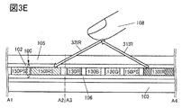
- 3A to 3D are diagrams showing examples of pixels of a display device.
- FIG. 3E is a cross-sectional view showing an example of an electronic device;
- FIG. 4 is a diagram showing an example of the layout of the display device.
- FIG. 5 is a diagram showing an example of the layout of the display device.
- FIG. 6 is a diagram showing an example of the layout of the display device.
- FIG. 7 is a diagram showing an example of the layout of the display device.
- FIG. 8 is a diagram showing an example of a pixel circuit.
- FIG. 9A is a top view showing an example of a display device.
- FIG. 9B is a cross-sectional view showing an example of a display device;
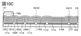
- 10A to 10D are diagrams illustrating an example of a method for manufacturing a display device.
- 11A to 11C are diagrams illustrating an example of a method for manufacturing a display device.
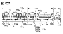
- 12A to 12C are diagrams illustrating an example of a method for manufacturing a display device.
- 13A to 13C are diagrams illustrating an example of a method for manufacturing a display device.
- FIG. 14 is a perspective view showing an example of a display device.
- FIG. 15A is a cross-sectional view showing an example of a display device;
- 15B and 15C are cross-sectional views showing examples of transistors.
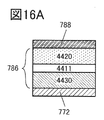
- 16A to 16D are diagrams showing configuration examples of light emitting devices.
- 17A and 17B are cross-sectional views showing examples of display devices.
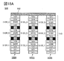
- 18A and 18B are cross-sectional views showing examples of display devices.
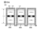
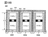
- 19A and 19B are cross-sectional views showing examples of display devices.
- 20A to 20C are cross-sectional views showing examples of display devices.
- 21A and 21B are diagrams illustrating examples of electronic devices.
- 22A to 22D are diagrams illustrating examples of electronic devices.
- 23A to 23F are diagrams illustrating examples of electronic devices.
- 24A and 24B are diagrams for explaining the evaluation method of the example.
- 25A and 25B are diagrams showing the evaluation results of Examples.
- FIG. 26 is a diagram showing evaluation results of Examples.
- FIG. 27 is a diagram showing evaluation results of Examples.
- FIG. 28 is a diagram showing evaluation results of Examples.
- FIG. 29 is a diagram showing evaluation results of Examples.
- film and “layer” can be interchanged depending on the case or situation.
- conductive layer can be changed to the term “conductive film.”
- insulating film can be changed to the term “insulating layer”.
- a display device of one embodiment of the present invention includes a first pixel including a light-emitting device, a first light-receiving device, and a second light-receiving device.
- a display device of one embodiment of the present invention can display an image using a light-emitting device.
- the first light receiving device has a smaller light receiving region area (also simply referred to as light receiving area) than the second light receiving device.
- the first light-receiving device can perform higher-definition imaging than the second light-receiving device.
- the first light receiving device can be used for imaging for personal authentication using a fingerprint, palm print, iris, pulse shape (including vein shape and artery shape), face, or the like.
- the first light receiving device can appropriately determine the wavelength of light to be detected according to the application.
- the first light receiving device preferably detects visible light.
- the second light receiving device can be used as a touch sensor (also referred to as a direct touch sensor) or a near touch sensor (also referred to as a hover sensor, hover touch sensor, non-contact sensor, or touchless sensor).
- the second light receiving device can appropriately determine the wavelength of light to be detected according to the application.
- the second light receiving device preferably detects infrared light (including near-infrared light). This enables touch detection even in dark places. Also, when the second light receiving device detects infrared light, it can detect dust or water droplets on the surface of the display device with high sensitivity compared to a capacitive touch sensor.
- a touch sensor or near-touch sensor can detect the proximity or contact of an object (such as a finger, hand, or pen).
- a touch sensor can detect an object by direct contact between the display device and the object.
- the near-touch sensor can detect the object even if the object does not touch the display device.
- the display device can detect the object when the distance between the display device and the object is 0.1 mm or more and 300 mm or less, preferably 3 mm or more and 50 mm or less.
- the display device can be operated without direct contact with the object, in other words, the display device can be operated without contact.
- the risk of staining or scratching the display device can be reduced, or the object can be displayed without directly touching the stain (for example, dust or virus) attached to the display device. It becomes possible to operate the device.
- the detection method of the object may be selected according to the function based on the difference in detection accuracy between the first light receiving device and the second light receiving device.
- the scrolling function of the display screen is realized by a near touch sensor function using the second light receiving device, and the input function with the keyboard displayed on the screen is a high-definition touch sensor using the first light receiving device. It may be implemented by a function.
- the first light-receiving device is preferably provided for all pixels included in the display device in order to perform high-definition imaging.
- the second light-receiving device used for a touch sensor, a near-touch sensor, or the like does not require high accuracy compared to detection using the first light-receiving device, and is provided in some pixels of the display device. It is good if there is The detection speed can be increased by reducing the number of the second light-receiving devices included in the display device compared to the number of the first light-receiving devices.
- a display device of one embodiment of the present invention can have a structure in which a plurality of each of the above first pixels and second pixels is provided.
- the second pixel is similar to the first pixel in that it has a light-emitting device and a first light-receiving device, and does not have a second light-receiving device, but instead has another device. and is different from the first pixel.
- the second pixel can have various sensor devices, or light emitting devices that emit infrared light, or the like. By providing the second pixel with a device different from that of the first pixel in this manner, the display device can be multifunctional.
- the display device of one embodiment of the present invention is preferably manufactured using the method for manufacturing the display device of one embodiment of the present invention, which is described in detail in Embodiment 2.
- the island-shaped EL layer is not formed using a fine metal mask, but is formed by forming an EL layer over one surface and then processing the EL layer. .
- the island-shaped EL layer is not formed using a fine metal mask, but is formed by forming an EL layer over one surface and then processing the EL layer. .
- the display device of one embodiment of the present invention can have a high aperture ratio, high definition, and multiple functions.
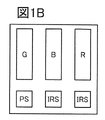
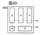
- FIG. 1A shows an example of a pixel included in a display device of one embodiment of the present invention.
- Pixel 180A shown in FIG. 1A has sub-pixel G, sub-pixel B, sub-pixel R, sub-pixel PS, and sub-pixel IRS.
- FIG. 1A shows an example in which one pixel 180A is provided over two rows and three columns.
- the pixel 180A has three sub-pixels (sub-pixel G, sub-pixel B, and sub-pixel R) in the upper row (first row) and two sub-pixels (sub-pixel R) in the lower row (second row).
- sub-pixel PS, sub-pixel IRS sub-pixel PS, sub-pixel IRS.
- the pixel 180A has two sub-pixels (sub-pixel G, sub-pixel PS) in the left column (first column) and sub-pixel B in the center column (second column). It has sub-pixels R in the right column (third column), and sub-pixels IRS from the center column to the right column. Note that the layout of sub-pixels is not limited to the configuration in FIG. 1A.
- the lower row may also have three sub-pixels (sub-pixel PS, two sub-pixels IRS).
- sub-pixel PS three sub-pixels
- IRS sub-pixels
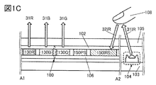
- 1C and 1D each illustrate an example of a cross-sectional view of an electronic device including a display device of one embodiment of the present invention.
- FIGS. 1C and 1D each have a display device 100 and a light source 104 between a housing 103 and a protective member 105.
- FIG. 1C The electronic devices shown in FIGS. 1C and 1D each have a display device 100 and a light source 104 between a housing 103 and a protective member 105.
- the light source 104 has a light emitting device that emits infrared light 31IR.
- a light emitting diode LED: Light Emitting Diode
- FIG. 1C shows an example in which the light source 104 is arranged at a position that does not overlap with the display device 100 . At this time, light emitted from the light source 104 is emitted to the outside of the electronic device through the protective member 105 .
- FIG. 1D shows an example in which the display device and the light source 104 are overlapped. At this time, light emitted from the light source 104 is emitted to the outside of the electronic device through the display device 100 and the protective member 105 .
- the display device 100 shown in FIGS. 1C and 1D corresponds to the cross-sectional structure along the dashed-dotted line A1-A2 in FIG. 1A.
- Display device 100 has a plurality of light emitting devices and a plurality of light receiving devices between substrate 106 and substrate 102 .
- Subpixel R has a light emitting device 130R that emits red light 31R.
- Subpixel G has a light emitting device 130G that emits green light 31G.
- Subpixel B has a light emitting device 130B that emits blue light 31B.
- the sub-pixel PS has a light receiving device 150PS and the sub-pixel IRS has a light receiving device 150IRS.
- the infrared light 31IR emitted by the light source 104 is reflected by the object 108 (finger here), and the reflected light 32IR from the object 108 is incident on the light receiving device 150IRS.
- the receiving device 150IRS can be used to detect the object 108 .
- the wavelength of light detected by light receiving device 150IRS is not particularly limited.
- the light receiving device 150IRS preferably detects infrared light.
- the light receiving device 150IRS may detect visible light, or both infrared light and visible light.
- detection of the object 108 may be performed using both the light receiving device 150PS and the light receiving device 150IRS.
- infrared light 31IR emitted by light source 104 is reflected by object 108 (here, a finger), and reflected light 32IR from object 108 is incident on light receiving device 150IRS. be done.
- green light 31G emitted by light emitting device 130G is also reflected by object 108, and reflected light 32G from object 108 is incident on light receiving device 150PS.
- the object 108 is not in contact with the electronics, the object 108 can be detected using the light receiving device 150IRS and the light receiving device 150PS.
- the light receiving device 150IRS (and the light receiving device 150PS) can also be used to detect the object 108 in contact with the electronic device.
- the light receiving area of the sub-pixel PS is smaller than the light receiving area of the sub-pixel IRS.
- the sub-pixels PS can be used to capture images for personal authentication using a fingerprint, palm print, iris, pulse shape (including vein shape and artery shape), face, or the like.
- green light 31G emitted by light emitting device 130G is reflected by object 108, and reflected light 32G from object 108 is incident on light receiving device 150PS.
- a fingerprint of the object 108 can be imaged using the light receiving device 150PS.
- green light 31G emitted by light emitting device 130G is used to detect an object by light receiving device 150PS, but the wavelength of light detected by light receiving device 150PS is not particularly limited.
- the light-receiving device 150PS preferably detects visible light, and preferably detects one or more of light having colors such as blue, purple, violet, green, yellow-green, yellow, orange, and red. Also, the light receiving device 150PS may detect infrared light.
- the light receiving device 150PS may have the function of detecting red light 31R emitted by the light emitting device 130R. Also, the light receiving device 150PS may have a function of detecting the blue light 31B emitted by the light emitting device 130B.
- the light-emitting device that emits the light detected by the light-receiving device 150PS is provided in a sub-pixel close to the sub-pixel PS in the pixel.
- the light receiving device 150PS detects light emitted from the light emitting device 130G of the subpixel G adjacent to the subpixel PS. With such a configuration, detection accuracy can be improved.
- all pixels may have the structure of the pixel 180A, some pixels may have the structure of the pixel 180A, and other pixels may have the structure of the pixel 180A. configuration may be applied.
- a display device of one embodiment of the present invention may include both the pixel 180A illustrated in FIG. 3A and the pixel 180B illustrated in FIG. 3B. Since the pixel 180A shown in FIG. 3A has the same configuration as the pixel 180A shown in FIG. 1A, detailed description thereof will be omitted.
- the pixel 180B shown in FIG. 3B has sub-pixel G, sub-pixel B, sub-pixel R, sub-pixel PS, and sub-pixel X.
- the pixel may have three sub-pixels (sub-pixel PS, two sub-pixels X) in the bottom row (second row).
- sub-pixel PS three sub-pixels
- X sub-pixels
- a device included in the sub-pixel X can be used to realize various functions in a display device or an electronic device equipped with the display device.
- a display device or an electronic device uses the device of the sub-pixel X to detect force, displacement, position, speed, acceleration, angular velocity, number of rotations, distance, magnetism, temperature, chemicals, time, hardness, electric field, current, and so on. , voltage, power, radiation, flow rate, humidity, gradient, vibration, smell, physical condition, pulse, body temperature, blood oxygen concentration, and arterial blood oxygen saturation.
- Functions of the display device or the electronic device include, for example, a strobe light function, a flash light function, a deterioration correction function, an acceleration sensor function, an odor sensor function, a physical condition detection function, a pulse detection function, a body temperature detection function, and a pulse oximeter. function, blood oxygen concentration measurement function, and the like.
- the strobe light function can be realized, for example, by repeating light emission and non-light emission in a short cycle.
- the flashlight function can be realized by, for example, a configuration that generates a flash of light by instantaneously discharging using the principle of an electric double layer or the like.
- the strobe light function and the flash light function can be used, for example, for security purposes or self-defense purposes.
- white is preferable as the emission color of the strobe light and the flash light.
- the practitioner can select one of the most suitable emission colors, such as white, blue, purple, blue-violet, green, yellow-green, yellow, orange, and red. Or you can select multiple.
- the deterioration correcting function there is a function of correcting the deterioration of the light-emitting device of at least one sub-pixel selected from the sub-pixel G, sub-pixel B, and sub-pixel R. More specifically, when the reliability of the material used for the light-emitting device included in the sub-pixel G is poor, the sub-pixel X has the same configuration as the sub-pixel G so that two sub-pixels G can be formed in the pixel 180B. can be provided. With this structure, the area of the sub-pixel G can be doubled. By doubling the area of the sub-pixel G, it is possible to increase the reliability by about two times compared to the configuration in which the sub-pixel G is one.
- the other sub-pixel G can be used to A configuration in which the light emission of the pixel G is supplemented may be employed.
- the sub-pixel G has been described above, the sub-pixel B and the sub-pixel R can also have the same configuration.
- the acceleration sensor function, the odor sensor function, the physical condition detection function, the pulse detection function, the body temperature detection function, and the blood oxygen concentration measurement function can be realized by providing the sub-pixel X with a sensor device necessary for detection. can. Further, it can be said that the display device or the electronic device can realize various functions according to the sensor device provided in the sub-pixel X.
- the display device having the pixel 180B can be called a multi-function display device or a multi-function panel.
- the function of the sub-pixel X may be one or two or more, and the operator can appropriately select the optimum function.
- the display device of one embodiment of the present invention may include a pixel including four subpixels, which does not include both the subpixel X and the subpixel IRS. That is, it may have a pixel having sub-pixel G, sub-pixel B, sub-pixel R, and sub-pixel PS. Further, the display device may have different numbers of sub-pixels depending on the pixel. On the other hand, in order to make the quality of each pixel uniform, it is preferable that all pixels have the same number of sub-pixels.
- the display device of one embodiment of the present invention may include both the pixel 180A illustrated in FIG. 3A and the pixel 180C illustrated in FIG. 3D.
- Pixel 180C shown in FIG. 3D has sub-pixel G, sub-pixel B, sub-pixel R, sub-pixel PS, and sub-pixel IR.
- Sub-pixel IR has a light-emitting device that emits infrared light. That is, the sub-pixel IR can be used as the light source of the sensor. Since the display device includes a light-emitting device that emits infrared light, it is not necessary to provide a light source separately from the display device, and the number of parts of the electronic device can be reduced.
- FIG. 3E illustrates an example of a cross-sectional view of an electronic device including a display device of one embodiment of the present invention.
- the electronic device shown in FIG. 3E has display device 100 between housing 103 and protective member 105 .
- the display device 100 shown in FIG. 3E corresponds to the cross-sectional structure along the dashed-dotted line A1-A2 in FIG. 3A and the cross-sectional structure along the dashed-dotted line A3-A4 in FIG. 3D. That is, the display device 100 shown in FIG. 3E has a pixel 180A and a pixel 180C.
- Subpixel R has a light emitting device 130R that emits red light 31R.
- Subpixel G has a light emitting device 130G that emits green light 31G.
- Subpixel B has a light emitting device 130B that emits blue light 31B.
- the sub-pixel PS has a light receiving device 150PS and the sub-pixel IRS has a light receiving device 150IRS.
- Subpixel IR has a light emitting device 130IR that emits infrared light 31IR.
- infrared light 31IR emitted by light emitting device 130IR is reflected by object 108 (here, a finger), and reflected light 32IR from object 108 enters light receiving device 150IRS.
- object 108 is not in contact with the electronics, the receiving device 150IRS can be used to detect the object 108 .
- 4 to 7 show an example of the layout of the display device.
- the near-touch sensor function for example, illuminates an object (such as a finger, hand, or pen) with a light source fixed at a specific location, detects reflected light from the object with a plurality of sub-pixels IRS, and detects a plurality of sub-pixels It can be realized by estimating the position of the object from the detection intensity ratio in the IRS.
- the pixels 180A having the sub-pixels IRS can be arranged in the display section at regular intervals, or arranged in the periphery of the display section.
- Driving frequency can be increased by performing near-touch detection using only some of the pixels.
- the sub-pixel X or the sub-pixel IR can be mounted in another pixel, the display device can be multi-functionalized.
- the display device 100A shown in FIG. 4 has two types of pixels: pixels 180A and pixels 180B.
- one pixel 180A is provided for 3 ⁇ 3 pixels (9 pixels), and the configuration of the pixel 180B is applied to the other pixels.
- the period of arranging the pixels 180A is not limited to one per 3 ⁇ 3 pixels.
- the pixels used for touch detection are 1 pixel per 4 pixels (2 ⁇ 2 pixels), 1 pixel per 16 pixels (4 ⁇ 4 pixels), 1 pixel per 100 pixels (10 ⁇ 10 pixels), or 900 pixels (30 pixels). x30 pixels) can be determined as appropriate.
- the display device 100B shown in FIG. 5 has two types of pixels: pixels 180A and pixels 180C.
- one pixel 180A is provided for 3 ⁇ 3 pixels (9 pixels), and the configuration of the pixel 180C is applied to the other pixels.
- the display device 100C shown in FIG. 6 has two types of pixels: pixels 180A and pixels 180B.
- the pixels 180A are provided on the periphery of the display portion, and the configuration of the pixels 180B is applied to the other pixels.
- the pixels 180A When the pixels 180A are provided around the periphery of the display portion, the pixels 180A may be arranged so as to surround all four sides as shown in FIG. can be arranged and various arrangements can be applied.
- the display device 100D shown in FIG. 7 has two types of pixels: pixels 180A and pixels 180C.
- the pixels 180A are provided on the periphery of the display portion, and the configuration of the pixels 180C is applied to the other pixels.
- infrared light 31IR emitted by a light source 104 provided outside the display unit of the display device is reflected by an object 108, and reflected light 32IR from the object 108 enters a plurality of pixels 180A. be done.
- the reflected light 32IR is detected by the sub-pixel IRS provided in the pixel 180A, and the position of the target object 108 can be estimated from the detection intensity ratio of the plurality of sub-pixels IRS.
- the light source 104 is provided at least outside the display portion of the display device, and may be built in the display device or may be mounted in an electronic device separately from the display device.
- a light emitting diode that emits infrared light can be used.
- the infrared light 31IR emitted by the sub-pixel IR of the pixel 180C is reflected by the target 108, and the reflected light 32IR from the target 108 enters the plurality of pixels 180A.
- the reflected light 32IR is detected by the sub-pixel IRS provided in the pixel 180A, and the position of the target object 108 can be estimated from the detection intensity ratio of the plurality of sub-pixels IRS.
- the layout of the display device can take various forms.
- FIG. 8 shows an example of a pixel circuit with two light receiving devices.
- the pixel shown in FIG. 8 comprises transistors M11, M12, M13, M14, M15, capacitor C1, and photodetectors PD1, PD2.
- the transistor M11 has a gate electrically connected to the wiring TX, one of its source and drain electrically connected to the anode electrode of the light receiving device PD1 and one of the source and drain of the transistor M15. The other is electrically connected to one of the source and drain of the transistor M12, the first electrode of the capacitor C1, and the gate of the transistor M13.
- the transistor M12 has a gate electrically connected to the wiring RS and the other of the source and the drain electrically connected to the wiring VRS.
- the transistor M13 has one of its source and drain electrically connected to the wiring VPI, and the other of its source and drain electrically connected to one of its source and drain of the transistor M14.
- the transistor M14 has a gate electrically connected to the wiring SE and the other of the source and the drain electrically connected to the wiring WX.
- the transistor M15 has a gate electrically connected to the wiring SW and the other of the source and the drain electrically connected to the anode electrode of the light receiving device PD1.
- Cathode electrodes of the light receiving device PD1 and the light receiving device PD2 are electrically connected to the wiring CL.
- a second electrode of the capacitor C1 is electrically connected to the wiring VCP.
- Transistor M11, transistor M12, transistor M14, and transistor M15 function as switches.
- the transistor M13 functions as an amplifying element (amplifier).
- all transistors included in a pixel circuit include a transistor including a metal oxide (also referred to as an oxide semiconductor) in a semiconductor layer in which a channel is formed (hereinafter also referred to as an OS transistor). It is preferable to use An OS transistor has extremely low off-state current and can hold charge accumulated in a capacitor connected in series with the transistor for a long time. Further, with the use of the OS transistor, power consumption of the display device can be reduced.
- a metal oxide also referred to as an oxide semiconductor
- an OS transistor has extremely low off-state current and can hold charge accumulated in a capacitor connected in series with the transistor for a long time. Further, with the use of the OS transistor, power consumption of the display device can be reduced.
- transistors including silicon in a semiconductor layer in which a channel is formed are preferably used for all the transistors included in the pixel circuit.
- silicon include monocrystalline silicon, polycrystalline silicon, amorphous silicon, and the like.
- a transistor including low-temperature polysilicon (LTPS) in a semiconductor layer hereinafter also referred to as an LTPS transistor.
- the LTPS transistor has high field effect mobility and can operate at high speed.
- the pixel circuit preferably includes an OS transistor and an LTPS transistor.
- OS transistor an OS transistor
- LTPS transistor an LTPS transistor
- LTPS transistors using low-temperature polysilicon for semiconductor layers are preferably used for all of the transistors M11 to M15.
- an OS transistor using a metal oxide for a semiconductor layer as the transistor M11, the transistor M12, and the transistor M15, and use an LTPS transistor as the transistor M13.
- an OS transistor or an LTPS transistor may be used as the transistor M14.
- the potential held at the gate of the transistor M13 changes based on the charges generated in the light receiving device PD1 and the light receiving device PD2. Leakage through transistor M15 can be prevented.
- an LTPS transistor is preferably used as the transistor M13.
- An LTPS transistor can achieve higher field-effect mobility than an OS transistor, and has excellent driving capability and current capability. Therefore, the transistor M13 can operate faster than the transistors M11, M12, and M15. By using an LTPS transistor for the transistor M13, it is possible to quickly output to the transistor M14 a minute potential based on the amount of light received by the light receiving device PD1 or the light receiving device PD2.
- the transistors M11, M12, and M15 have a small leakage current, and the transistor M13 has a high driving capability. And the charge transferred through the transistor M15 can be held without leaking, and reading can be performed at high speed.
- the transistor M14 functions as a switch that passes the output from the transistor M13 to the wiring WX, unlike the transistors M11 to M13 and the transistor M15, low off-state current, high-speed operation, and the like are not necessarily required. Therefore, low-temperature polysilicon or an oxide semiconductor may be applied to the semiconductor layer of the transistor M14.
- transistors are shown as n-channel transistors in FIGS. 8A and 8B, p-channel transistors can also be used.
- the aperture ratio (light-receiving area) of the light-receiving device is small.
- the aperture ratio (light receiving area) of the light receiving device is large. Therefore, it is preferable that the aperture ratio (light-receiving area) of the light-receiving device PD1 is smaller than the aperture ratio (light-receiving area) of the light-receiving device PD2.
- imaging that requires high definition it is preferable to perform imaging using only the light receiving device PD1 by turning on the transistor M11 and turning off the transistor M15.
- the display device of the present embodiment can add two functions in addition to the display function by mounting two types of light receiving devices in one pixel. Functionalization becomes possible. For example, it is possible to realize a high-definition imaging function and a sensing function such as a touch sensor or a near-touch sensor. In addition, by combining a pixel equipped with two types of light receiving devices and a pixel with another configuration, the functions of the display device can be further increased. For example, a light-emitting device that emits infrared light, or a pixel having various sensor devices can be used.
- a display device of one embodiment of the present invention includes a light-emitting device and a light-receiving device in a pixel.
- pixels have a light-receiving function, contact or proximity of an object can be detected while displaying an image. For example, in addition to displaying an image with all the sub-pixels of the display device, some sub-pixels exhibit light as a light source, some other sub-pixels perform light detection, and the remaining sub-pixels You can also display images with
- light-emitting devices are arranged in matrix in the display portion, and an image can be displayed on the display portion.
- light receiving devices are arranged in a matrix in the display section, and the display section has one or both of an imaging function and a sensing function in addition to an image display function.
- the display part can be used for an image sensor or a touch sensor. That is, by detecting light on the display portion, an image can be captured, or proximity or contact of an object (a finger, hand, pen, or the like) can be detected.
- the display device of one embodiment of the present invention can use a light-emitting device as a light source of a sensor. Therefore, it is not necessary to provide a light receiving portion and a light source separately from the display device, and the number of parts of the electronic device can be reduced.
- the light-receiving device when an object reflects (or scatters) light emitted by a light-emitting device included in the display portion, the light-receiving device can detect the reflected light (or scattered light).
- the reflected light or scattered light.
- imaging or touch detection is possible.
- a display device of one embodiment of the present invention has a function of displaying an image using a light-emitting device.
- the light-emitting device functions as a display device (also referred to as a display element).
- Light-emitting devices include, for example, OLEDs (Organic Light Emitting Diodes) and QLEDs (Quantum-dot Light Emitting Diodes).
- Examples of light-emitting substances included in the light-emitting device include substances that emit fluorescence (fluorescent materials), substances that emit phosphorescence (phosphorescent materials), inorganic compounds (quantum dot materials, etc.), and substances that exhibit thermally activated delayed fluorescence (heat Activated delayed fluorescence (Thermally Activated Delayed Fluorescence: TADF) material).
- LEDs such as micro LED (Light Emitting Diode), can also be used as a light emitting device.
- a display device of one embodiment of the present invention has a function of detecting light using a light-receiving device.
- the display device can capture an image using the light receiving device.
- the display device of this embodiment can be used as a scanner.
- an image sensor can be used to acquire biometric data such as fingerprints and palm prints. That is, the biometric authentication sensor can be incorporated in the display device.
- the biometric authentication sensor can be incorporated into the display device.
- the display device can detect proximity or contact of an object using the light receiving device.
- a pn-type or pin-type photodiode can be used as the light receiving device.
- a light-receiving device functions as a photoelectric conversion device (also referred to as a photoelectric conversion element) that detects light incident on the light-receiving device and generates an electric charge. The amount of charge generated from the light receiving device is determined based on the amount of light incident on the light receiving device.
- organic photodiode having a layer containing an organic compound as the light receiving device.
- Organic photodiodes can be easily made thinner, lighter, and larger, and have a high degree of freedom in shape and design, so that they can be applied to various display devices.
- an organic EL device is used as the light-emitting device and an organic photodiode is used as the light-receiving device.
- An organic EL device and an organic photodiode can be formed on the same substrate. Therefore, an organic photodiode can be incorporated in a display device using an organic EL device.
- the organic photodiode has many layers that can have the same configuration as the organic EL device, the layers that can have the same configuration can be formed at once, thereby suppressing an increase in the number of film forming steps.
- one of the pair of electrodes can be a layer common to the light receiving device and the light emitting device.
- at least one of the hole injection layer, the hole transport layer, the electron transport layer, and the electron injection layer is preferably a layer common to the light receiving device and the light emitting device.
- a layer shared by the light-receiving device and the light-emitting device may have different functions in the light-emitting device and in the light-receiving device. Components are referred to herein based on their function in the light emitting device.
- a hole-injecting layer functions as a hole-injecting layer in light-emitting devices and as a hole-transporting layer in light-receiving devices.
- an electron-injecting layer functions as an electron-injecting layer in light-emitting devices and as an electron-transporting layer in light-receiving devices.
- a layer shared by the light-receiving device and the light-emitting device may have the same function in the light-emitting device as in the light-receiving device.
- a hole-transporting layer functions as a hole-transporting layer in both a light-emitting device and a light-receiving device
- an electron-transporting layer functions as an electron-transporting layer in both a light-emitting device and a light-receiving device.
- an island-shaped light-emitting layer can be formed by a vacuum evaporation method using a metal mask (also referred to as a shadow mask).
- a metal mask also referred to as a shadow mask.
- island-like formations occur due to various influences such as precision of the metal mask, misalignment between the metal mask and the substrate, bending of the metal mask, and broadening of the contour of the deposited film due to vapor scattering. Since the shape and position of the light-emitting layer deviate from the design, it is difficult to increase the definition and aperture ratio of the display device.
- an island-shaped pixel electrode (which can also be called a lower electrode) is formed, and a first layer (EL layer or EL layer) including a light-emitting layer that emits light of a first color is formed. layer) is formed over the entire surface, a first sacrificial layer is formed on the first layer. Then, a first resist mask is formed over the first sacrificial layer, and the first layer and the first sacrificial layer are processed using the first resist mask, thereby forming an island-shaped first layer.
- a second layer (which can be called an EL layer or part of an EL layer) including a light-emitting layer that emits light of a second color is formed as a second sacrificial layer. and an island shape using a second resist mask.
- the island-shaped EL layer is not formed using a fine metal mask, but is processed after the EL layer is formed over one surface. It is formed. Therefore, it is possible to realize a high-definition display device or a display device with a high aperture ratio, which has hitherto been difficult to achieve. Furthermore, since the EL layer can be separately formed for each color, a display device with extremely vivid, high-contrast, and high-quality display can be realized.
- a sacrificial layer (which may also be referred to as a mask layer) over the EL layer, damage to the EL layer during the manufacturing process of the display device can be reduced, and the reliability of the light-emitting device can be improved.
- the pattern of the EL layer itself (which can also be called a processing size) can be made much smaller than when a metal mask is used.
- the thickness of the EL layer varies between the center and the edge, so the effective area that can be used as the light emitting region is smaller than the area of the EL layer. Become.
- the manufacturing method described above since the EL layer is formed by processing a film formed to have a uniform thickness, the thickness can be made uniform within the EL layer, and even a fine pattern can be formed in almost the entire area. can be used as the light emitting region. Therefore, a display device having both high definition and high aperture ratio can be manufactured.
- the first layer and the second layer each include at least a light-emitting layer, and preferably consist of a plurality of layers. Specifically, it is preferable to have one or more layers on the light-emitting layer.
- the light-emitting layer can be prevented from being exposed to the outermost surface during the manufacturing process of the display device, and damage to the light-emitting layer can be reduced. This can improve the reliability of the light emitting device.
- a light-emitting device that emits light of different colors, it is not necessary to separately form all the layers constituting the EL layer, and some of the layers can be formed in the same process.
- the sacrificial layer is removed, and the remaining layers forming the EL layer are shared.
- An electrode also referred to as an upper electrode is formed in common for the light emitting devices of each color.
- a manufacturing method similar to that for the light-emitting device can also be applied to the light-receiving device.
- the island-shaped active layer (also called photoelectric conversion layer) of the light receiving device is not formed using a fine metal mask, but is formed by forming a film that will become the active layer over the surface and then processing it. Therefore, the island-shaped active layer can be formed with a uniform thickness. Further, by providing the sacrificial layer over the active layer, the damage to the active layer during the manufacturing process of the display device can be reduced, and the reliability of the light receiving device can be improved.
- FIG. 9A and 9B illustrate a display device of one embodiment of the present invention.
- FIG. 9A shows a top view of the display device 100E.
- the display device 100E has a display section in which a plurality of pixels 110 are arranged in a matrix and a connection section 140 outside the display section.
- One pixel 110 is composed of five sub-pixels 110a, 110b, 110c, 110d, and 110e.
- the connection portion 140 can also be called a cathode contact portion.
- the top surface shape of the sub-pixel shown in FIG. 9A corresponds to the top surface shape of the light emitting region or the light receiving region.
- the circuit layout forming the sub-pixels is not limited to the range of the sub-pixels shown in FIG. 9A, and may be arranged outside the sub-pixels.
- the transistors included in sub-pixel 110a may be located within sub-pixel 110b shown in FIG. 9A, or some or all may be located outside sub-pixel 110a.
- FIG. 9A shows that the subpixels 110a, 110b, and 110c have the same aperture ratio (which can also be called the size or the size of the light-emitting region) or approximately the same, one embodiment of the present invention is not limited thereto.
- the aperture ratios of the sub-pixels 110a, 110b, 110c, 110d, and 110e can be determined as appropriate.
- the aperture ratios of the sub-pixels 110a, 110b, 110c, 110d, and 110e may be different, and two or more may be equal or substantially equal.
- FIG. 9A shows an example in which one pixel 110 is provided over two rows and three columns.
- the pixel 110 has three sub-pixels (sub-pixels 110a, 110b, 110c) in the upper row (first row) and two sub-pixels (sub-pixels 110d, 110d, 110c) in the lower row (second row). 110e).
- pixel 110 has two sub-pixels (sub-pixels 110a and 110d) in the left column (first column), has sub-pixel 110b in the center column (second column), and has sub-pixel 110b in the middle column (second column). It has a sub-pixel 110c in the column (third column), and further has sub-pixels 110e from the center column to the right column.
- sub-pixels 110a, 110b, and 110c each have light-emitting devices that emit light of different colors
- sub-pixels 110d and 110e each have light-receiving devices with different light-receiving areas.
- sub-pixels 110a, 110b, and 110c correspond to sub-pixels G, B, and R shown in FIG. 1A and the like.
- the sub-pixel 110d corresponds to the sub-pixel PS shown in FIG. 1A and the like
- the sub-pixel 110e corresponds to the sub-pixel IRS shown in FIG. 1A and the like.
- sub-pixel 110e may be changed for each pixel.
- some sub-pixels 110e may correspond to sub-pixels IRS, and other sub-pixels 110e may correspond to sub-pixels X (see FIG. 3B) or sub-pixels IR (see FIG. 3D).
- FIG. 9A shows an example in which the connection portion 140 is positioned below the display portion in a top view, but the present invention is not particularly limited.
- the connecting portion 140 may be provided at least one of the upper side, the right side, the left side, and the lower side of the display portion when viewed from above, and may be provided so as to surround the four sides of the display portion.
- the number of connection parts 140 may be singular or plural.
- FIG. 9B shows cross-sectional views along dashed-dotted lines X1-X2, Y1-Y2, and Y3-Y4 in FIG. 9A.
- the display device 100E includes light-emitting devices 130a, 130b, 130c and light-receiving devices 150d (see FIG. 13B) and 150e on a layer 101 including transistors, and covers the light-emitting device and the light-receiving device.
- a protective layer 131 is provided as shown in FIG.
- a substrate 120 is bonded onto the protective layer 131 with a resin layer 122 .
- a display device of one embodiment of the present invention is a top emission type in which light is emitted in a direction opposite to a substrate over which a light-emitting device is formed, and light is emitted toward a substrate over which a light-emitting device is formed.
- a bottom emission type bottom emission type
- a double emission type dual emission type in which light is emitted from both sides may be used.
- the layer 101 including transistors for example, a stacked-layer structure in which a plurality of transistors are provided over a substrate and an insulating layer is provided to cover the transistors can be applied.
- a structural example of the layer 101 including a transistor will be described later in Embodiment 3.
- Light emitting devices 130a, 130b, 130c each emit different colors of light.
- Light-emitting devices 130a, 130b, and 130c are preferably a combination that emits three colors of light, red (R), green (G), and blue (B), for example.
- a light-emitting device has an EL layer between a pair of electrodes.
- one of a pair of electrodes may be referred to as a pixel electrode and the other may be referred to as a common electrode.
- one electrode functions as an anode and the other electrode functions as a cathode.
- the pixel electrode functions as an anode and the common electrode functions as a cathode will be described below as an example.
- the light-emitting device 130a has a pixel electrode 111a on the layer 101 containing the transistor, a first layer 113a on the pixel electrode 111a, a sixth layer 114 on the first layer 113a, and a sixth layer 114 on the sixth layer 114. and a common electrode 115 .
- the first layer 113a and the sixth layer 114 can be collectively called an EL layer.
- the first layer 113a includes a first hole-injection layer 181a on the pixel electrode 111a, a first hole-transport layer 182a on the first hole-injection layer 181a, and a first hole-transport layer 182a. It has a first light emitting layer 183a on top and a first electron transport layer 184a on the first light emitting layer 183a.
- the sixth layer 114 has, for example, an electron injection layer.
- the sixth layer 114 may have a laminate of an electron transport layer and an electron injection layer.
- the light-emitting device 130b has a pixel electrode 111b on the layer 101 containing the transistor, a second layer 113b on the pixel electrode 111b, a sixth layer 114 on the second layer 113b, and a sixth layer 114 on the sixth layer 114. and a common electrode 115 .
- the second layer 113b and the sixth layer 114 can be collectively called an EL layer.
- the second layer 113b includes a second hole-injection layer 181b over the pixel electrode 111b, a second hole-transport layer 182b over the second hole-injection layer 181b, and a second hole-transport layer 182b. It has a second light emitting layer 183b on top and a second electron transport layer 184b on the second light emitting layer 183b.
- the light-emitting device 130c has a pixel electrode 111c on the layer 101 containing the transistor, a third layer 113c on the pixel electrode 111c, a sixth layer 114 on the third layer 113c, and a sixth layer 114 on the sixth layer 114. and a common electrode 115 .
- the third layer 113c and the sixth layer 114 can be collectively referred to as EL layers.
- the third layer 113c includes a third hole-injection layer 181c over the pixel electrode 111c, a third hole-transport layer 182c over the third hole-injection layer 181c, and a third hole-transport layer 182c. It has a third light-emitting layer 183c on top and a third electron-transporting layer 184c on the third light-emitting layer 183c.
- Light emitting devices 130a, 130b, 130c each emit different colors of light.
- Light-emitting devices 130a, 130b, and 130c are preferably a combination that emits three colors of light, red (R), green (G), and blue (B), for example.
- a light receiving device has an active layer between a pair of electrodes.
- one of a pair of electrodes may be referred to as a pixel electrode and the other may be referred to as a common electrode.
- one electrode functions as an anode and the other electrode functions as a cathode.
- the pixel electrode functions as an anode and the common electrode functions as a cathode will be described below as an example. That is, the light-receiving device can be driven by applying a reverse bias between the pixel electrode and the common electrode to detect light incident on the light-receiving device, generate charges, and extract them as current.
- the light receiving device 150d includes a pixel electrode 111d on the layer 101 including the transistor, a fourth layer 113d on the pixel electrode 111d, and a sixth layer 114 on the fourth layer 113d. , and a common electrode 115 on the sixth layer 114 .
- the fourth layer 113d includes a fourth hole-transport layer 182d on the pixel electrode 111d, a first active layer 185d on the fourth hole-transport layer 182d, and a fourth layer 185d on the first active layer 185d. and an electron transport layer 184d of .
- a sixth layer 114 is a layer common to the light-emitting device and the light-receiving device.
- the sixth layer 114 comprises, for example, an electron injection layer, as described above.
- the sixth layer 114 may have a laminate of an electron transport layer and an electron injection layer.
- a layer shared by the light-receiving device and the light-emitting device may have different functions in the light-emitting device and in the light-receiving device. Components are sometimes referred to herein based on their function in the light emitting device.
- a hole-injecting layer functions as a hole-injecting layer in light-emitting devices and as a hole-transporting layer in light-receiving devices.
- an electron-injecting layer functions as an electron-injecting layer in light-emitting devices and as an electron-transporting layer in light-receiving devices.
- a layer shared by the light-receiving device and the light-emitting device may have the same function in the light-emitting device as in the light-receiving device.
- a hole-transporting layer functions as a hole-transporting layer in both a light-emitting device and a light-receiving device
- an electron-transporting layer functions as an electron-transporting layer in both a light-emitting device and a light-receiving device.
- the light receiving device 150e includes a pixel electrode 111e on the layer 101 including the transistor, a fifth layer 113e on the pixel electrode 111e, a sixth layer 114 on the fifth layer 113e, and a and a common electrode 115 .
- the fifth layer 113e includes a fifth hole-transport layer 182e on the pixel electrode 111e, a second active layer 185e on the fifth hole-transport layer 182e, and a fifth layer 185e on the second active layer 185e. and an electron transport layer 184e of
- the common electrode 115 is electrically connected to the conductive layer 123 provided in the connecting portion 140 . As a result, the same potential is supplied to the common electrodes 115 of the light emitting devices of each color.
- a conductive film that transmits visible light and infrared light is used for the electrode on the light extraction side of the pixel electrode and the common electrode.
- a conductive film that reflects visible light and infrared light is preferably used for the electrode on the side from which light is not extracted.
- metals, alloys, electrically conductive compounds, mixtures thereof, and the like can be used as appropriate.
- indium tin oxide also referred to as In—Sn oxide, ITO
- In—Si—Sn oxide also referred to as ITSO
- indium zinc oxide In—Zn oxide
- In—W— Zn oxides aluminum-containing alloys (aluminum alloys) such as alloys of aluminum, nickel, and lanthanum (Al-Ni-La)
- Al-Ni-La aluminum-containing alloys
- Al-Ni-La alloys of silver, palladium and copper
- APC alloys of silver, palladium and copper
- elements belonging to Group 1 or Group 2 of the periodic table of elements not exemplified above e.g., lithium (Li), cesium (Cs), calcium (Ca), strontium (Sr)), europium (Eu), ytterbium
- Yb rare earth metal
- an alloy containing an appropriate combination thereof, graphene, or the like can be used.
- a micro optical resonator (microcavity) structure is preferably applied to the light emitting device and the light receiving device. Therefore, one of the pair of electrodes included in the light-emitting device and the light-receiving device preferably has an electrode (semi-transmissive/semi-reflective electrode) that is transparent and reflective to visible light, and the other is reflective to visible light. It is preferable to have an electrode (reflective electrode) having a Since the light-emitting device has a microcavity structure, the light emitted from the light-emitting layer can be resonated between both electrodes, and the light emitted from the light-emitting device can be enhanced. Since the light receiving device has a microcavity structure, the light received by the active layer can be resonated between the two electrodes, the light can be strengthened, and the detection accuracy of the light receiving device can be improved.
- the semi-transmissive/semi-reflective electrode can have a laminated structure of a reflective electrode and an electrode (also referred to as a transparent electrode) having transparency to visible light.
- the light transmittance of the transparent electrode is set to 40% or more.
- the light-emitting device preferably uses an electrode having a transmittance of 40% or more for visible light (light with a wavelength of 400 nm or more and less than 750 nm).
- the visible light reflectance of the semi-transmissive/semi-reflective electrode is 10% or more and 95% or less, preferably 30% or more and 80% or less.
- the visible light reflectance of the reflective electrode is 40% or more and 100% or less, preferably 70% or more and 100% or less.
- the resistivity of these electrodes is preferably 1 ⁇ 10 ⁇ 2 ⁇ cm or less.
- the transmittance or reflectance of near-infrared light (light having a wavelength of 750 nm or more and 1300 nm or less) of these electrodes preferably satisfies the above numerical range, similarly to the transmittance or reflectance of visible light.
- the first layer 113a, the second layer 113b, and the third layer 113c each have a light-emitting layer.
- the first layer 113a, the second layer 113b, and the third layer 113c preferably have light-emitting layers that emit light of different colors.
- a light-emitting layer is a layer containing a light-emitting substance.
- the emissive layer can have one or more emissive materials.
- a substance exhibiting emission colors such as blue, purple, violet, green, yellow-green, yellow, orange, and red is used as appropriate.
- a substance that emits near-infrared light can be used as the light-emitting substance.
- Examples of light-emitting substances include fluorescent materials, phosphorescent materials, thermally activated delayed fluorescence (TADF) materials, and quantum dot materials.
- fluorescent materials include fluorescent materials, phosphorescent materials, thermally activated delayed fluorescence (TADF) materials, and quantum dot materials.
- TADF thermally activated delayed fluorescence
- fluorescent materials include pyrene derivatives, anthracene derivatives, triphenylene derivatives, fluorene derivatives, carbazole derivatives, dibenzothiophene derivatives, dibenzofuran derivatives, dibenzoquinoxaline derivatives, quinoxaline derivatives, pyridine derivatives, pyrimidine derivatives, phenanthrene derivatives, and naphthalene derivatives. be done.
- Examples of phosphorescent materials include organometallic complexes (especially iridium complexes) having a 4H-triazole skeleton, 1H-triazole skeleton, imidazole skeleton, pyrimidine skeleton, pyrazine skeleton, or pyridine skeleton, and phenylpyridine derivatives having an electron-withdrawing group.
- organometallic complexes especially iridium complexes
- platinum complexes, rare earth metal complexes, etc. which are used as ligands, can be mentioned.
- the light-emitting layer may contain one or more organic compounds (host material, assist material, etc.) in addition to the light-emitting substance (guest material).
- One or both of a hole-transporting material and an electron-transporting material can be used as the one or more organic compounds.
- Bipolar materials or TADF materials may also be used as one or more organic compounds.
- the light-emitting layer preferably includes, for example, a phosphorescent material and a combination of a hole-transporting material and an electron-transporting material that easily form an exciplex.
- ExTET Exciplex-Triplet Energy Transfer
- a combination that forms an exciplex that emits light that overlaps with the wavelength of the absorption band on the lowest energy side of the light-emitting substance energy transfer becomes smooth and light emission can be efficiently obtained. With this configuration, high efficiency, low-voltage driving, and long life of the light-emitting device can be realized at the same time.
- the first layer 113a, the second layer 113b, and the third layer 113c include, as layers other than the light-emitting layer, a substance with a high hole-injection property, a substance with a high hole-transport property, a hole-blocking material, and an electron layer.
- a layer containing a highly transportable substance, a highly electron-injecting substance, an electron-blocking material, a bipolar substance (a substance with high electron-transporting and hole-transporting properties), or the like may be further included.
- Both low-molecular-weight compounds and high-molecular-weight compounds can be used in the light-emitting device, and inorganic compounds may be included.
- Each of the layers constituting the light-emitting device can be formed by a vapor deposition method (including a vacuum vapor deposition method), a transfer method, a printing method, an inkjet method, a coating method, or the like.
- the first layer 113a, the second layer 113b, and the third layer 113c are respectively a hole-injecting layer, a hole-transporting layer, a hole-blocking layer, an electron-blocking layer, an electron-transporting layer, and an electron layer. It may have one or more of the injection layers.
- the sixth layer 114 can have one or more of a hole injection layer, a hole transport layer, a hole blocking layer, an electron blocking layer, an electron transport layer, and an electron injection layer.
- a hole injection layer e.g., a hole transport layer
- a hole blocking layer e.g., a hole blocking layer
- an electron injection layer e.g., a hole blocking layer
- the hole-injecting layer is a layer that injects holes from the anode to the hole-transporting layer, and contains a material with high hole-injecting properties.
- highly hole-injecting materials include aromatic amine compounds and composite materials containing a hole-transporting material and an acceptor material (electron-accepting material).
- a hole-transporting layer is a layer that transports holes injected from the anode by the hole-injecting layer to the light-emitting layer.
- the hole-transporting layer is a layer that transports holes generated by incident light in the active layer to the anode.
- a hole-transporting layer is a layer containing a hole-transporting material.
- the hole-transporting material a substance having a hole mobility of 1 ⁇ 10 ⁇ 6 cm 2 /Vs or more is preferable. Note that substances other than these can be used as long as they have a higher hole-transport property than electron-transport property.
- hole-transporting materials include ⁇ -electron-rich heteroaromatic compounds (e.g., carbazole derivatives, thiophene derivatives, furan derivatives, etc.), aromatic amines (compounds having an aromatic amine skeleton), and other highly hole-transporting materials. is preferred.
- ⁇ -electron-rich heteroaromatic compounds e.g., carbazole derivatives, thiophene derivatives, furan derivatives, etc.
- aromatic amines compounds having an aromatic amine skeleton
- other highly hole-transporting materials is preferred.
- an electron-transporting layer is a layer that transports electrons injected from the cathode by the electron-injecting layer to the light-emitting layer.
- the electron transport layer is a layer that transports electrons generated by incident light in the active layer to the cathode.
- the electron-transporting layer is a layer containing an electron-transporting material.
- an electron-transporting material a substance having an electron mobility of 1 ⁇ 10 ⁇ 6 cm 2 /Vs or more is preferable. Note that substances other than these substances can be used as long as they have a higher electron-transport property than hole-transport property.
- electron-transporting materials include metal complexes having a quinoline skeleton, metal complexes having a benzoquinoline skeleton, metal complexes having an oxazole skeleton, metal complexes having a thiazole skeleton, oxadiazole derivatives, triazole derivatives, imidazole derivatives, ⁇ -electrons including oxazole derivatives, thiazole derivatives, phenanthroline derivatives, quinoline derivatives with quinoline ligands, benzoquinoline derivatives, quinoxaline derivatives, dibenzoquinoxaline derivatives, pyridine derivatives, bipyridine derivatives, pyrimidine derivatives, and other nitrogen-containing heteroaromatic compounds
- a material having a high electron-transport property such as a deficient heteroaromatic compound can be used.
- the electron injection layer is a layer that injects electrons from the cathode into the electron transport layer, and is a layer containing a material with high electron injection properties.
- Alkali metals, alkaline earth metals, or compounds thereof can be used as materials with high electron injection properties.
- a composite material containing an electron-transporting material and a donor material (electron-donating material) can also be used as a material with high electron-injecting properties.
- Examples of the electron injection layer include lithium, cesium, lithium fluoride (LiF), cesium fluoride (CsF), calcium fluoride (CaF 2 ), 8-(quinolinolato)lithium (abbreviation: Liq), 2-(2 -pyridyl)phenoratritium (abbreviation: LiPP), 2-(2-pyridyl)-3-pyridinolatritium (abbreviation: LiPPy), 4-phenyl-2-(2-pyridyl)phenoratritium (abbreviation: LiPPP) , lithium oxide (LiO x ), cesium carbonate, etc., alkali metals, alkaline earth metals, or compounds thereof.
- Liq lithium, cesium, lithium fluoride
- CsF cesium fluoride
- CaF 2 calcium fluoride
- Liq 8-(quinolinolato)lithium
- LiPP 2-(2 -pyridyl)phenoratritium
- an electron-transporting material may be used as the electron injection layer.
- a compound having a lone pair of electrons and an electron-deficient heteroaromatic ring can be used as the electron-transporting material.
- a compound having at least one of a pyridine ring, diazine ring (pyrimidine ring, pyrazine ring, pyridazine ring), and triazine ring can be used.
- the lowest unoccupied molecular orbital (LUMO) of the organic compound having an unshared electron pair is preferably ⁇ 3.6 eV or more and ⁇ 2.3 eV or less.
- CV cyclic voltammetry
- photoelectron spectroscopy optical absorption spectroscopy
- inverse photoelectron spectroscopy etc. are used to determine the highest occupied molecular orbital (HOMO: Highest Occupied Molecular Orbital) level and LUMO level of an organic compound. can be estimated.
- BPhen 4,7-diphenyl-1,10-phenanthroline
- NBPhen 2,9-bis(naphthalen-2-yl)-4,7-diphenyl-1,10-phenanthroline
- HATNA diquinoxalino [2,3-a:2′,3′-c]phenazine
- TmPPPyTz 2,4,6-tris[3′-(pyridin-3-yl)biphenyl-3-yl]-1,3 , 5-triazine
- TmPPPyTz 2,4,6-tris[3′-(pyridin-3-yl)biphenyl-3-yl]-1,3 , 5-triazine
- the fourth layer 113d and the fifth layer 113e each have an active layer.
- the fourth layer 113d and the fifth layer 113e may have active layers with the same configuration or may have active layers with different configurations.
- a microcavity structure can be produced by changing the thickness of the pixel electrode or the thickness of the optical adjustment layer in the light receiving devices 150d and 150e. In this case, the fourth layer 113d and the fifth layer 113e may have the same configuration.
- the first active layer 185d and the second active layer 185e each contain a semiconductor.
- the semiconductor include inorganic semiconductors such as silicon and organic semiconductors including organic compounds.
- an organic semiconductor is used as the semiconductor included in the active layer.
- the light-emitting layer and the active layer can be formed by the same method (for example, a vacuum deposition method), and a manufacturing apparatus can be shared, which is preferable.
- Electron-accepting organic semiconductor materials such as fullerenes (eg, C 60 , C 70 , etc.) and fullerene derivatives can be used as the n-type semiconductor material of the active layer.
- Fullerenes have a soccer ball-like shape, which is energetically stable.
- Fullerene has both deep (low) HOMO and LUMO levels. Since fullerene has a deep LUMO level, it has an extremely high electron-accepting property (acceptor property).
- acceptor property Normally, like benzene, when the ⁇ -electron conjugation (resonance) spreads in the plane, the electron-donating property (donor property) increases. , the electron acceptability becomes higher.
- a high electron-accepting property is useful as a light-receiving device because charge separation occurs quickly and efficiently.
- Both C 60 and C 70 have broad absorption bands in the visible light region, and C 70 is particularly preferable because it has a larger ⁇ -electron conjugated system than C 60 and has a wide absorption band in the long wavelength region.
- [6,6]-Phenyl-C71-butylic acid methyl ester (abbreviation: PC70BM), [6,6]-Phenyl-C61-butylic acid methyl ester (abbreviation: PC60BM), 1′, 1′′,4′,4′′-Tetrahydro-di[1,4]methanonaphthaleno[1,2:2′,3′,56,60:2′′,3′′][5,6]fullerene- C60 (abbreviation: ICBA) etc. are mentioned.
- Materials for the n-type semiconductor include metal complexes having a quinoline skeleton, metal complexes having a benzoquinoline skeleton, metal complexes having an oxazole skeleton, metal complexes having a thiazole skeleton, oxadiazole derivatives, triazole derivatives, imidazole derivatives, Oxazole derivatives, thiazole derivatives, phenanthroline derivatives, quinoline derivatives, benzoquinoline derivatives, quinoxaline derivatives, dibenzoquinoxaline derivatives, pyridine derivatives, bipyridine derivatives, pyrimidine derivatives, naphthalene derivatives, anthracene derivatives, coumarin derivatives, rhodamine derivatives, triazine derivatives, quinone derivatives, etc. is mentioned.
- Materials for the p-type semiconductor of the active layer include copper (II) phthalocyanine (CuPc), tetraphenyldibenzoperiflanthene (DBP), zinc phthalocyanine (ZnPc), and tin phthalocyanine.
- electron-donating organic semiconductor materials such as (SnPc) and quinacridone;
- Examples of p-type semiconductor materials include carbazole derivatives, thiophene derivatives, furan derivatives, and compounds having an aromatic amine skeleton.
- materials for p-type semiconductors include naphthalene derivatives, anthracene derivatives, pyrene derivatives, triphenylene derivatives, fluorene derivatives, pyrrole derivatives, benzofuran derivatives, benzothiophene derivatives, indole derivatives, dibenzofuran derivatives, dibenzothiophene derivatives, indolocarbazole derivatives, porphyrin derivatives, phthalocyanine derivatives, naphthalocyanine derivatives, quinacridone derivatives, polyphenylenevinylene derivatives, polyparaphenylene derivatives, polyfluorene derivatives, polyvinylcarbazole derivatives, polythiophene derivatives and the like.
- the HOMO level of the electron-donating organic semiconductor material is preferably shallower (higher) than the HOMO level of the electron-accepting organic semiconductor material.
- the LUMO level of the electron-donating organic semiconductor material is preferably shallower (higher) than the LUMO level of the electron-accepting organic semiconductor material.
- a spherical fullerene as the electron-accepting organic semiconductor material and an organic semiconductor material having a nearly planar shape as the electron-donating organic semiconductor material. Molecules with similar shapes tend to gather together, and when molecules of the same type aggregate, the energy levels of the molecular orbitals are close to each other, so the carrier transportability can be enhanced.
- the active layer is preferably formed by co-depositing an n-type semiconductor and a p-type semiconductor.
- the active layer may be formed by laminating an n-type semiconductor and a p-type semiconductor.
- the fourth layer 113d and the fifth layer 113e are layers other than the active layer, which are highly hole-transporting substances, highly electron-transporting substances, or bipolar substances (electron-transporting and hole-transporting substances). It may further have a layer containing, for example, a substance with a high degree of resistance. Further, the fourth layer 113d and the fifth layer 113e may have various functional layers that can be used for the first layer 113a, the second layer 113b and the third layer 113c. good.
- Either a low-molecular-weight compound or a high-molecular-weight compound can be used for the light-receiving device, and an inorganic compound may be included.
- the layers constituting the light-receiving device can be formed by methods such as a vapor deposition method (including a vacuum vapor deposition method), a transfer method, a printing method, an inkjet method, and a coating method.
- hole-transporting materials include polymer compounds such as poly(3,4-ethylenedioxythiophene)/poly(styrenesulfonic acid) (PEDOT/PSS), molybdenum oxide, and copper iodide (CuI).
- Inorganic compounds such as can be used.
- an inorganic compound such as zinc oxide (ZnO) can be used as the electron-transporting material.
- 6-diyl]-2,5-thiophenediyl[5,7-bis(2-ethylhexyl)-4,8-dioxo-4H,8H-benzo[1,2-c:4,5-c′]dithiophene-1 ,3-diyl]]polymer (abbreviation: PBDB-T) or a polymer compound such as a PBDB-T derivative can be used.
- a method of dispersing an acceptor material in PBDB-T or a PBDB-T derivative can be used.
- three or more kinds of materials may be mixed in the active layer.
- a third material may be mixed in addition to the n-type semiconductor material and the p-type semiconductor material.
- the third material may be a low-molecular compound or a high-molecular compound.
- a protective layer 131 on the light emitting devices 130a, 130b, 130c and the light receiving devices 150d, 150e.
- the conductivity of the protective layer 131 does not matter. At least one of an insulating film, a semiconductor film, and a conductive film can be used as the protective layer 131 .
- the protective layer 131 Since the protective layer 131 has an inorganic film, it prevents oxidation of the common electrode 115, suppresses the entry of impurities (moisture, oxygen, etc.) into the light-emitting devices 130a, 130b, 130c and the light-receiving devices 150d, 150e. Degradation of the light emitting device and the light receiving device can be suppressed, and the reliability of the display device can be improved.
- an inorganic insulating film such as an oxide insulating film, a nitride insulating film, an oxynitride insulating film, or a nitride oxide insulating film can be used.
- the oxide insulating film include a silicon oxide film, an aluminum oxide film, a gallium oxide film, a germanium oxide film, an yttrium oxide film, a zirconium oxide film, a lanthanum oxide film, a neodymium oxide film, a hafnium oxide film, a tantalum oxide film, and the like.
- nitride insulating film examples include a silicon nitride film and an aluminum nitride film.
- oxynitride insulating film a silicon oxynitride film, an aluminum oxynitride film, or the like can be given.
- nitride oxide insulating film a silicon nitride oxide film, an aluminum nitride oxide film, or the like can be given.
- oxynitride refers to a material whose composition contains more oxygen than nitrogen
- nitride oxide refers to a material whose composition contains more nitrogen than oxygen. point to the material.
- the protective layer 131 preferably has a nitride insulating film or a nitride oxide insulating film, and more preferably has a nitride insulating film.
- the protective layer 131 contains ITO, In—Zn oxide, Ga—Zn oxide, Al—Zn oxide, indium gallium zinc oxide (also referred to as In—Ga—Zn oxide, IGZO), or the like.
- Inorganic membranes can also be used.
- the inorganic film preferably has a high resistance, and specifically, preferably has a higher resistance than the common electrode 115 .
- the inorganic film may further contain nitrogen.
- the protective layer 131 When the light emitted from the light-emitting device is taken out through the protective layer 131, the protective layer 131 preferably has high transparency to visible light.
- the protective layer 131 preferably has high transparency to visible light.
- ITO, IGZO, and aluminum oxide are preferable because they are inorganic materials with high transparency to visible light.
- the protective layer 131 for example, a stacked structure of an aluminum oxide film and a silicon nitride film over the aluminum oxide film, or a stacked structure of an aluminum oxide film and an IGZO film over the aluminum oxide film, or the like can be used. can be done. By using the stacked structure, entry of impurities (water, oxygen, or the like) into the EL layer can be suppressed.
- the protective layer 131 may have an organic film.
- protective layer 131 may have both an organic film and an inorganic film.
- Each end of the pixel electrodes 111 a , 111 b , 111 c is covered with an insulating layer 121 .
- a device manufactured using a metal mask or FMM may be referred to as a device with an MM (metal mask) structure.
- a device manufactured without using a metal mask or FMM may be referred to as a device with an MML (metal maskless) structure.
- a structure in which a light-emitting layer is separately formed or a light-emitting layer is separately painted in each color light-emitting device is referred to as SBS (Side By Side) structure.
- SBS Side By Side
- a light-emitting device capable of emitting white light is sometimes referred to as a white light-emitting device.
- a white light emitting device can be combined with a colored layer (for example, a color filter) to realize a full-color display device.
- light-emitting devices can be broadly classified into a single structure and a tandem structure.
- a single-structure device preferably has one light-emitting unit between a pair of electrodes, and the light-emitting unit preferably includes one or more light-emitting layers.
- the light-emitting unit preferably includes one or more light-emitting layers.
- the luminescent color of the first luminescent layer and the luminescent color of the second luminescent layer have a complementary color relationship, it is possible to obtain a configuration in which the entire light emitting device emits white light.
- a device with a tandem structure preferably has two or more light-emitting units between a pair of electrodes, and each light-emitting unit includes one or more light-emitting layers.
- each light-emitting unit includes one or more light-emitting layers.
- a structure in which white light emission is obtained by combining light from the light emitting layers of a plurality of light emitting units may be employed. Note that the structure for obtaining white light emission is the same as the structure of the single structure.
- the white light emitting device when comparing the white light emitting device (single structure or tandem structure) and the light emitting device having the SBS structure, the light emitting device having the SBS structure can consume less power than the white light emitting device. If it is desired to keep power consumption low, it is preferable to use a light-emitting device with an SBS structure. On the other hand, the white light emitting device is preferable because the manufacturing process is simpler than that of the SBS structure light emitting device, so that the manufacturing cost can be lowered or the manufacturing yield can be increased.
- the distance between the light-emitting devices can be reduced.
- the distance between the light emitting devices is 1 ⁇ m or less, preferably 500 nm or less, more preferably 200 nm or less, 100 nm or less, 90 nm or less, 70 nm or less, 50 nm or less, 30 nm or less, 20 nm or less, 15 nm or less, or 10 nm.
- the display device of this embodiment has a gap between the side surface of the first layer 113a and the side surface of the second layer 113b, or a gap between the side surface of the second layer 113b and the side surface of the third layer 113c. It has regions with a spacing of 1 ⁇ m or less, preferably 0.5 ⁇ m (500 nm) or less, and more preferably 100 nm or less.
- the distance between the light-emitting device and the light-receiving device can also be within the above range. Also, in order to suppress leakage between the light emitting device and the light receiving device, it is preferable to make the distance between the light emitting device and the light receiving device wider than the distance between the light emitting devices. For example, the distance between the light emitting device and the light receiving device can be 8 ⁇ m or less, 5 ⁇ m or less, or 3 ⁇ m or less.
- FIGS. 10A to 10D show side by side a cross-sectional view along dashed line X1-X2, a cross-sectional view along X3-X4, and a cross-sectional view along Y1-Y2 in FIG. 9A. 11 to 13 are also the same as FIG.
- Thin films (insulating films, semiconductor films, conductive films, etc.) that make up the display device are formed by sputtering, chemical vapor deposition (CVD), vacuum deposition, pulsed laser deposition (PLD). ) method, ALD method, or the like.
- CVD methods include a plasma enhanced CVD (PECVD) method, a thermal CVD method, and the like. Also, one of the thermal CVD methods is the metal organic CVD (MOCVD) method.
- thin films that make up the display device can be applied by spin coating, dipping, spray coating, inkjet, dispensing, screen printing, offset printing, doctor knife, slit coating, roll coating, It can be formed by methods such as curtain coating and knife coating.
- a vacuum process such as a vapor deposition method and a solution process such as a spin coating method or an inkjet method can be used for manufacturing a light-emitting device.
- vapor deposition methods include physical vapor deposition (PVD) such as sputtering, ion plating, ion beam vapor deposition, molecular beam vapor deposition, and vacuum vapor deposition, and chemical vapor deposition (CVD).
- the functional layers (hole injection layer, hole transport layer, light emitting layer, electron transport layer, electron injection layer, etc.) included in the EL layer may be formed by a vapor deposition method (vacuum vapor deposition method, etc.), a coating method (dip coating method, die coat method, bar coat method, spin coat method, spray coat method, etc.), printing method (inkjet method, screen (stencil printing) method, offset (lithographic printing) method, flexographic (letterpress printing) method, gravure method, or micro contact method, etc.).
- a vapor deposition method vacuum vapor deposition method, etc.
- a coating method dip coating method, die coat method, bar coat method, spin coat method, spray coat method, etc.
- printing method inkjet method, screen (stencil printing) method, offset (lithographic printing) method, flexographic (letterpress printing) method, gravure method, or micro contact method, etc.
- a photolithography method or the like can be used when processing a thin film forming a display device.
- the thin film may be processed by a nanoimprint method, a sandblast method, a lift-off method, or the like.
- an island-shaped thin film may be directly formed by a film formation method using a shielding mask such as a metal mask.
- the photolithography method there are typically the following two methods.
- One is a method of forming a resist mask on a thin film to be processed, processing the thin film by etching or the like, and removing the resist mask.
- the other is a method of forming a photosensitive thin film, then performing exposure and development to process the thin film into a desired shape.
- the light used for exposure can be, for example, i-line (wavelength 365 nm), g-line (wavelength 436 nm), h-line (wavelength 405 nm), or a mixture thereof.
- ultraviolet rays, KrF laser light, ArF laser light, or the like can also be used.
- extreme ultraviolet (EUV: Extreme Ultra-violet) light or X-rays may be used.
- An electron beam can also be used instead of the light used for exposure. The use of extreme ultraviolet light, X-rays, or electron beams is preferable because extremely fine processing is possible.
- a photomask is not necessary when exposure is performed by scanning a beam such as an electron beam.
- a dry etching method, a wet etching method, a sandblasting method, or the like can be used for etching the thin film.
- pixel electrodes 111a, 111b, 111c, 111d, and 111e and a conductive layer 123 are formed over a layer 101 including transistors.
- Each pixel electrode is provided in the display portion, and the conductive layer 123 is provided in the connection portion 140 .
- an insulating layer 121 is formed to cover end portions of the pixel electrodes 111a, 111b, 111c, 111d, and 111e and end portions of the conductive layer 123 .
- a first hole injection layer 181A, a first hole transport layer 182A, a first light emitting layer 183A, and a first light emitting layer 183A are formed. are formed in this order, a first sacrificial layer 118A is formed on the first electron transport layer 184A, and a second sacrificial layer 119A is formed on the first sacrificial layer 118A.
- the present invention is not limited to this.
- the first hole-injection layer 181A, the first hole-transport layer 182A, the first light-emitting layer 183A, the first electron-transport layer 184A, and the first sacrificial layer 118A overlap with the conductive layer 123. It doesn't have to be. Further, end portions of the first hole-injection layer 181A, the first hole-transport layer 182A, the first light-emitting layer 183A, and the first electron-transport layer 184A on the side of the connection portion 140 are the first sacrificial layers. 118A and the end of the second sacrificial layer 119A may be located inside. For example, by using a mask (also referred to as an area mask, a rough metal mask, etc.
- a mask also referred to as an area mask, a rough metal mask, etc.
- the first hole injection layer 181A and the first hole transport layer are formed.
- 182A, the first light-emitting layer 183A, the first electron-transporting layer 184A, and the first sacrificial layer 118A and the second sacrificial layer 119A can be deposited in different regions.
- a light-emitting device is formed using a resist mask. By combining with an area mask as described above, a light-emitting device can be manufactured through a relatively simple process.
- a sputtering method or a vacuum deposition method can be used to form the pixel electrode.
- the insulating layer 121 can have a single-layer structure or a laminated structure using one or both of an inorganic insulating film and an organic insulating film.
- organic insulating materials that can be used for the insulating layer 121 include acrylic resins, epoxy resins, polyimide resins, polyamide resins, polyimideamide resins, polysiloxane resins, benzocyclobutene resins, and phenol resins.
- an inorganic insulating film that can be used for the insulating layer 121 an inorganic insulating film that can be used for the protective layer 131 can be used.
- an inorganic insulating film is used as the insulating layer 121 covering the edge of the pixel electrode, impurities are less likely to enter the light-emitting device than when an organic insulating film is used, and the reliability of the light-emitting device can be improved.
- the step coverage is higher and the shape of the pixel electrode is less likely to affect the step coverage than when an inorganic insulating film is used. Therefore, short-circuiting of the light emitting device can be prevented.
- the shape of the insulating layer 121 can be processed into a tapered shape or the like.
- a tapered shape refers to a shape in which at least part of a side surface of a structure is inclined with respect to a substrate surface or a formation surface.
- the insulating layer 121 may not be provided. By not providing the insulating layer 121, the aperture ratio of the sub-pixel can be increased in some cases. Alternatively, the distance between sub-pixels can be reduced, which may increase the definition or resolution of the display.
- the first hole-injection layer 181A, the first hole-transport layer 182A, the first light-emitting layer 183A, and the first electron-transport layer 184A are respectively later referred to as the first hole-injection layer 181a, the first These layers are to be the hole-transporting layer 182a, the first light-emitting layer 183a, and the first electron-transporting layer 184a. Therefore, the above-described structures applicable to the first hole-injection layer 181a, the first hole-transport layer 182a, the first light-emitting layer 183a, and the first electron-transport layer 184a can be applied.
- the first hole-injecting layer 181A, the first hole-transporting layer 182A, the first light-emitting layer 183A, and the first electron-transporting layer 184A are each formed by vapor deposition (including vacuum vapor deposition), transfer method, It can be formed by a method such as a printing method, an inkjet method, or a coating method. Also, the first hole injection layer 181A, the first hole transport layer 182A, the first light emitting layer 183A, and the first electron transport layer 184A may each be formed using a premix material. . In this specification and the like, a premix material is a composite material in which a plurality of materials are blended or mixed in advance.
- the sacrificial layer has a two-layer structure of a first sacrificial layer and a second sacrificial layer.
- the sacrificial layer includes a first hole-injection layer 181A, a first hole-transport layer 182A, a first light-emitting layer 183A, a first electron-transport layer 184A, and various functional layers formed in later steps.
- a film (a hole injection layer, a hole transport layer, a light-emitting layer, an electron transport layer, an active layer, etc.) having high resistance to processing conditions, specifically, a film having a high etching selectivity is used.
- sputtering sputtering, ALD (including thermal ALD and PEALD), or vacuum deposition can be used to form the sacrificial layer.
- ALD including thermal ALD and PEALD
- vacuum deposition can be used to form the sacrificial layer.
- a formation method that causes less damage to the EL layer is preferable, and the sacrificial layer is preferably formed by an ALD method or a vacuum evaporation method rather than a sputtering method.
- a film that can be removed by a wet etching method is preferably used for the sacrificial layer.
- the wet etching method By using the wet etching method, the first hole injection layer 181A, the first hole transport layer 182A, the first light emitting layer 183A, and the first hole injection layer 181A, the first hole transport layer 182A, and the first light emitting layer 183A are easily etched during processing of the sacrificial layer, compared to the case of using the dry etching method. Damage to the first electron transport layer 184A can be reduced.
- various functional layers hole injection layer, hole transport layer, light emitting layer, active layer, and electron It is desirable that the transport layer, etc.) is difficult to process, and that various sacrificial layers are difficult to process in the process of processing the functional layer. It is desirable to select the material of the sacrificial layer, the processing method, and the processing method of the functional layer in consideration of these.
- an inorganic film such as a metal film, an alloy film, a metal oxide film, a semiconductor film, or an inorganic insulating film can be used.
- the sacrificial layer includes metal materials such as gold, silver, platinum, magnesium, nickel, tungsten, chromium, molybdenum, iron, cobalt, copper, palladium, titanium, aluminum, yttrium, zirconium, and tantalum, or the metal materials.
- metal materials such as gold, silver, platinum, magnesium, nickel, tungsten, chromium, molybdenum, iron, cobalt, copper, palladium, titanium, aluminum, yttrium, zirconium, and tantalum, or the metal materials.
- a metal oxide such as an In--Ga--Zn oxide can be used for the sacrificial layer.
- the sacrificial layer for example, an In--Ga--Zn oxide film can be formed using a sputtering method.
- indium oxide, In-Zn oxide, In-Sn oxide, indium titanium oxide (In-Ti oxide), indium tin zinc oxide (In-Sn-Zn oxide), indium titanium zinc oxide ( In--Ti--Zn oxide), indium gallium tin-zinc oxide (In--Ga--Sn--Zn oxide), or the like can be used.
- indium tin oxide containing silicon or the like can be used.
- element M is aluminum, silicon, boron, yttrium, copper, vanadium, beryllium, titanium, iron, nickel, germanium, zirconium, molybdenum, lanthanum, cerium, neodymium, hafnium, tantalum, tungsten , or one or more selected from magnesium
- M is aluminum, silicon, boron, yttrium, copper, vanadium, beryllium, titanium, iron, nickel, germanium, zirconium, molybdenum, lanthanum, cerium, neodymium, hafnium, tantalum, tungsten , or one or more selected from magnesium
- various inorganic insulating films that can be used for the protective layer 131 can be used as the sacrificial layer.
- an oxide insulating film is preferable because it has higher adhesion to the EL layer than a nitride insulating film.
- inorganic insulating materials such as aluminum oxide, hafnium oxide, and silicon oxide can be used for the sacrificial layer.
- an aluminum oxide film can be formed using the ALD method. Use of the ALD method is preferable because damage to the base (especially the EL layer or the like) can be reduced.
- a lamination structure of an In—Ga—Zn oxide film formed by a sputtering method and an aluminum oxide film formed on the In—Ga—Zn oxide film by an ALD method is applied as the sacrificial layer.
- a lamination structure of an aluminum oxide film formed by an ALD method and an In--Ga--Zn oxide film formed over the aluminum oxide film by a sputtering method can be used as the sacrificial layer.
- a single-layer structure of an aluminum oxide film formed by an ALD method can be applied as the sacrificial layer.
- a resist mask 190a is formed on the second sacrificial layer 119A.
- a resist mask can be formed by applying a photosensitive resin (photoresist), followed by exposure and development.
- the resist mask 190a is provided at a position overlapping with the pixel electrode 111a.
- the resist mask 190a preferably does not overlap with the pixel electrodes 111b, 111c, 111d, and 111e.
- the resist mask 190a preferably does not overlap with the conductive layer 123.
- the resist mask 190a is It is preferably provided at a position overlapping with the conductive layer 123 . As a result, damage to the conductive layer 123 in subsequent steps can be suppressed.
- a resist mask 190a is used to partially remove the second sacrificial layer 119A.
- a region of the second sacrificial layer 119A that does not overlap with the resist mask 190a can be removed. Therefore, the second sacrificial layer 119a remains at the position overlapping with the pixel electrode 111a. After that, the resist mask 190a is removed.
- the second sacrificial layer 119a is used to partially remove the first sacrificial layer 118A.
- the region of the first sacrificial layer 118A that does not overlap with the second sacrificial layer 119a can be removed. Therefore, a laminated structure of the first sacrificial layer 118a and the second sacrificial layer 119a remains at the position overlapping with the pixel electrode 111a.
- a portion of the first hole injection layer 181A and a portion of the first hole transport layer 182A are formed.
- a portion of the first light-emitting layer 183A and a portion of the first electron-transporting layer 184A are removed.
- the first sacrificial layer 118a and the second sacrificial layer of the first hole injection layer 181A, the first hole transport layer 182A, the first light emitting layer 183A, and the first electron transport layer 184A are formed. Areas not overlapping layer 119a can be removed.
- the pixel electrodes 111b, 111c, 111d, 111e and the conductive layer 123 are exposed. Then, on the pixel electrode 111a, a first hole-injection layer 181a, a first hole-transport layer 182a, a first light-emitting layer 183a, a first electron-transport layer 184a, a first sacrificial layer 118a, and A laminated structure of the second sacrificial layer 119a remains. Note that the stacked structure of the first hole-injection layer 181a, the first hole-transport layer 182a, the first light-emitting layer 183a, and the first electron-transport layer 184a is also referred to as the first layer 113a.
- the first sacrificial layer 118A and the second sacrificial layer 119A can be processed by wet etching or dry etching, respectively.
- the first sacrificial layer 118A and the second sacrificial layer 119A are preferably processed by anisotropic etching.
- the first hole injection layer 181A, the first hole transport layer 182A, the first light emitting layer 183A, and the first hole injection layer 181A, the first hole transport layer 182A, and the first light emitting layer 183A are easily etched during processing of the sacrificial layer, compared to the case of using the dry etching method. , damage to the first electron transport layer 184A can be reduced.
- a developer for example, a tetramethylammonium hydroxide (TMAH) aqueous solution, dilute hydrofluoric acid, oxalic acid, phosphoric acid, acetic acid, nitric acid, or a chemical solution using a mixed liquid thereof can be used.
- TMAH tetramethylammonium hydroxide
- the first hole-injection layer 181A, the first hole-transport layer 182A, the first light-emitting layer 183A, and the first hole-injection layer 183A, and Degradation of the first electron transport layer 184A can be suppressed.
- a gas containing a noble gas such as CF 4 , C 4 F 8 , SF 6 , CHF 3 , Cl 2 , H 2 O, BCl 3 , or He is used for etching. Gases are preferred.
- the sacrificial layer has a laminated structure, some layers are processed using the resist mask 190a, and after removing the resist mask 190a, the partial layers are used as a hard mask to process the remaining layers. be able to.
- the resist mask 190a is removed by ashing using oxygen plasma or the like.
- the first sacrificial layer 118A is located on the outermost surface, and the first hole injection layer 181A, the first hole transport layer 182A, the first light emitting layer 183A, and the first electron transport layer 184A are formed. are not exposed, the first hole-injection layer 181A, the first hole-transport layer 182A, the first light-emitting layer 183A, and the first electron-transport layer 184A are exposed in the step of removing the resist mask 190a. You can prevent damage from occurring.
- the first sacrificial layer 118A can be processed.
- One hole-injection layer 181A, first hole-transport layer 182A, first light-emitting layer 183A, and first electron-transport layer 184A can be processed.
- the first hole injection layer 181A, the first hole transport layer 182A, the first light emitting layer 183A, and the first electron transport layer 184A are preferably processed by anisotropic etching.
- Anisotropic dry etching is particularly preferred.
- As an etching gas a gas containing nitrogen, a gas containing hydrogen, a gas containing noble gas, a gas containing nitrogen and argon, a gas containing nitrogen and hydrogen, or the like is preferably used.
- a gas containing oxygen By not using a gas containing oxygen as an etching gas, deterioration of the first hole-injection layer 181A, the first hole-transport layer 182A, the first light-emitting layer 183A, and the first electron-transport layer 184A can be prevented. can be suppressed.
- a gas containing oxygen may be used as the etching gas.
- the etching gas contains oxygen, the etching rate can be increased. Therefore, etching can be performed under low power conditions while maintaining a sufficiently high etching rate. Therefore, damage to the first hole-injection layer 181A, the first hole-transport layer 182A, the first light-emitting layer 183A, and the first electron-transport layer 184A can be suppressed. Furthermore, problems such as adhesion of reaction products that occur during etching can be suppressed.
- a second hole-injecting layer 181B and a second hole-transporting layer are formed on the second sacrificial layer 119a, the pixel electrodes 111b, 111c, 111d, and 111e, and the insulating layer 121.
- a layer 182B, a second light-emitting layer 183B, and a second electron-transporting layer 184B are formed in this order, a first sacrificial layer 118B is formed on the second electron-transporting layer 184B, and a first sacrificial layer 118B is formed.
- a second sacrificial layer 119B is formed thereon.
- the second hole-injection layer 181B, the second hole-transport layer 182B, the second light-emitting layer 183B, and the second electron-transport layer 184B are later formed into the second hole-injection layer 181b and the second electron-transport layer 184B, respectively. These layers are to be the hole-transporting layer 182b, the second light-emitting layer 183b, and the second electron-transporting layer 184b.
- the second light emitting layer 183b emits light of a color different from that of the first light emitting layer 183a.
- the structures, materials, and the like that can be applied to the second hole-injection layer 181b, the second hole-transport layer 182b, the second light-emitting layer 183b, and the second electron-transport layer 184b are the Similar to layer 181a, first hole-transporting layer 182a, first light-emitting layer 183a, and first electron-transporting layer 184a.
- the second hole-transport layer 182B, the second light-emitting layer 183B, and the second electron-transport layer 184B are the first hole-injection layer 181A, the first hole-transport layer 182A, and the first light-emitting layer, respectively.
- Layer 183A and the first electron-transporting layer 184A can be deposited using a similar method.
- the first sacrificial layer 118B and the second sacrificial layer 119B can be formed using a material applicable to the first sacrificial layer 118A and the second sacrificial layer 119A.
- a resist mask 190b is formed on the first sacrificial layer 118B.
- the resist mask 190b is provided at a position overlapping with the pixel electrode 111b.
- a resist mask 190b is used to partially remove the second sacrificial layer 119B.
- a region of the second sacrificial layer 119B that does not overlap with the resist mask 190b can be removed. Therefore, the second sacrificial layer 119b remains at the position overlapping with the pixel electrode 111b. After that, the resist mask 190b is removed.
- the first sacrificial layer 118b is formed by processing the first sacrificial layer 118B using the second sacrificial layer 119b as a hard mask. Then, using the first sacrificial layer 118b and the second sacrificial layer 119b as hard masks, a second hole-injection layer 181B, a second hole-transport layer 182B, a second light-emitting layer 183B, and By processing the second electron-transporting layer 184B, a second hole-injecting layer 181b, a second hole-transporting layer 182b, a second light-emitting layer 183b, and a second electron-transporting layer 184b are formed. .
- the stacked structure of the second hole-injection layer 181b, the second hole-transport layer 182b, the second light-emitting layer 183b, and the second electron-transport layer 184b is also referred to as a second layer 113b.
- the first sacrificial layer 118B and the second sacrificial layer 119B can be processed using a method applicable to the processing of the first sacrificial layer 118A and the second sacrificial layer 119A.
- the second hole-injection layer 181B, the second hole-transport layer 182B, the second light-emitting layer 183B, and the second electron-transport layer 184B are the first hole-injection layer 181A and the first hole-transport layer. It can be processed using methods applicable to the processing of layer 182A, first light-emitting layer 183A, and first electron-transporting layer 184A.
- the resist mask 190b can be removed by a method and timing applicable to removing the resist mask 190a.
- a stacked structure of a third layer 113c, a first sacrificial layer 118c, and a second sacrificial layer 119c is formed on the pixel electrode 111c, and a fourth layer 113d is formed on the pixel electrode 111d.
- a first sacrificial layer 118d, and a second sacrificial layer 119d are formed, and a fifth layer 113e, a first sacrificial layer 118e, and a second sacrificial layer 119e are formed on the pixel electrode 111e.
- a laminated structure In this embodiment, an example in which the fourth layer 113d and the fifth layer 113e have different structures is shown. It can be made in a process.
- the resist mask provided for forming the fifth layer 113 e is preferably provided so as to overlap with the conductive layer 123 .
- a laminated structure of the first sacrificial layer 118e and the second sacrificial layer 119e remains on the conductive layer 123 as shown in FIG. 12C.
- Such a structure is preferable because the conductive layer 123 can be prevented from being damaged in the next step of removing the first sacrificial layer and the second sacrificial layer.
- the first sacrificial layers 118a, 118b, 118c, 118d, 118e and the second sacrificial layers 119a, 119b, 119c, 119d, 119e are removed.
- the first electron-transporting layer 184a is exposed on the pixel electrode 111a
- the second electron-transporting layer 184b is exposed on the pixel electrode 111b
- the third electron-transporting layer 184c is exposed on the pixel electrode 111c.
- the fourth electron-transporting layer 184d is exposed on the pixel electrode 111d
- the fifth electron-transporting layer 184e is exposed on the pixel electrode 111e
- the conductive layer 123 is exposed on the connection portion 140.
- the same method as in the sacrificial layer processing step can be used.
- the first layer 113a, the second layer 113b, the third layer 113c, and the fourth layer can be removed more easily than when the dry etching method is used. Damage to 113d and fifth layer 113e can be reduced.
- a sixth layer 114 is formed and a common electrode 115 is formed over the sixth layer 114 , the insulating layer 121 and the conductive layer 123 .
- each of the layers constituting the sixth layer 114 can be formed by a vapor deposition method (including a vacuum vapor deposition method), a transfer method, a printing method, an inkjet method, a coating method, or the like. Also, the layers constituting the sixth layer 114 may be formed using a premix material. Note that the sixth layer 114 may be omitted if unnecessary.
- common electrode 115 Materials that can be used for the common electrode 115 are as described above.
- a sputtering method or a vacuum deposition method can be used.
- a protective layer 131 is formed on the common electrode 115 .
- the protective layer 131 Materials that can be used for the protective layer 131 are as described above. Methods for forming the protective layer 131 include a vacuum deposition method, a sputtering method, a CVD method, an ALD method, and the like.
- the protective layer 131 may have a single layer structure or a laminated structure. For example, the protective layer 131 may have a laminated structure of two layers formed using different film formation methods.
- FIG. 13B shows an example in which the sixth layer 114 enters a region between the first layer 113a and the second layer 113b. may be formed.
- the voids 133 contain, for example, one or more selected from air, nitrogen, oxygen, carbon dioxide, and group 18 elements (typically helium, neon, argon, xenon, krypton, etc.).
- the refractive index of the air gap 133 is lower than the refractive index of the sixth layer 114 , the light emitted from the light emitting device will be reflected at the interface between the sixth layer 114 and the air gap 133 .
- the display device 100E shown in FIG. 9B can be manufactured.
- the island-shaped EL layer is not formed using a fine metal mask, but is formed by forming an EL layer over one surface and then processing the EL layer. Therefore, the island-shaped EL layer can be formed with a uniform thickness.
- each EL layer can be manufactured with a configuration (material, film thickness, etc.) suitable for each color light-emitting device. Thereby, a light-emitting device with good characteristics can be produced.
- the display device of this embodiment can be a high-resolution display device or a large-sized display device. Therefore, the display device of the present embodiment includes a relatively large screen such as a television device, a desktop or notebook personal computer, a computer monitor, a digital signage, a large game machine such as a pachinko machine, or the like. In addition to electronic devices, it can be used for display portions of digital cameras, digital video cameras, digital photo frames, mobile phones, portable game machines, personal digital assistants, and sound reproducing devices.
- FIG. 14 shows a perspective view of the display device 100F
- FIG. 15A shows a cross-sectional view of the display device 100F.
- the display device 100F has a configuration in which a substrate 152 and a substrate 151 are bonded together.
- the substrate 152 is clearly indicated by dashed lines.
- the display device 100F includes a display portion 162, a circuit 164, wirings 165, and the like.
- FIG. 14 shows an example in which an IC 173 and an FPC 172 are mounted on the display device 100F. Therefore, the configuration shown in FIG. 14 can also be said to be a display module including the display device 100F, an IC (integrated circuit), and an FPC.
- a scanning line driver circuit can be used.
- the wiring 165 has a function of supplying signals and power to the display portion 162 and the circuit 164 .
- the signal and power are input to the wiring 165 from the outside through the FPC 172 or input to the wiring 165 from the IC 173 .
- FIG. 14 shows an example in which an IC 173 is provided on a substrate 151 by a COG (Chip On Glass) method, a COF (Chip On Film) method, or the like.
- a COG Chip On Glass
- COF Chip On Film
- the IC 173 for example, an IC having a scanning line driver circuit or a signal line driver circuit can be applied.
- the display device 100F and the display module may be configured without an IC.
- the IC may be mounted on the FPC by the COF method or the like.
- FIG. 15A shows an example of a cross section of the display device 100F when a portion of the region including the FPC 172, a portion of the circuit 164, a portion of the display portion 162, and a portion of the region including the edge are cut. show.
- a display device 100F illustrated in FIG. 15A includes a transistor 201, a transistor 205a, a transistor 205e, a light emitting device 130a, a light receiving device 150e, and the like between substrates 151 and 152.
- FIG. Light emitting device 130a emits red, green, or blue light, for example. Alternatively, light emitting device 130a may emit infrared light.
- the light receiving device 150e detects infrared light, for example. Alternatively, the light receiving device 150e may detect visible light, or both visible light and infrared light.
- the three sub-pixels include sub-pixels of three colors of R, G, and B, yellow ( Y), cyan (C), and magenta (M) sub-pixels.
- the four sub-pixels include R, G, B, and white (W) sub-pixels, and R, G, B, and Y four-color sub-pixels. be done.
- the protective layer 131 and the substrate 152 are adhered via the adhesive layer 142 .
- a solid sealing structure, a hollow sealing structure, or the like can be applied to sealing the light-emitting device.
- the space between substrates 152 and 151 is filled with an adhesive layer 142 to apply a solid sealing structure.
- the space may be filled with an inert gas (such as nitrogen or argon) to apply a hollow sealing structure.
- the adhesive layer 142 may be provided so as not to overlap the light emitting device.
- the space may be filled with a resin different from the adhesive layer 142 provided in a frame shape.
- the light emitting device 130a has a layered structure similar to that of the light emitting device 130a shown in FIG. 9B, and the light receiving device 150e has a layered structure similar to that of the light receiving device 150e shown in FIG. 9B.
- Embodiment 2 can be referred to for details of the light emitting device and the light receiving device.
- the end of the light emitting device 130a and the end of the light receiving device 150e are each covered with a protective layer 131. As shown in FIG.
- the pixel electrodes 111a and 111e are connected to conductive layers 222b of the transistors 205a and 205e through openings provided in the insulating layer 214, respectively.
- the pixel electrode contains a material that reflects visible light
- the common electrode contains a material that transmits visible light
- Light emitted by the light emitting device is emitted to the substrate 152 side. Also, the light receiving device detects light incident from the substrate 152 side. Therefore, for the substrate 152, it is preferable to use a material having high transparency to visible light and infrared light.
- a stacked structure from the substrate 151 to the insulating layer 214 corresponds to the layer 101 including the transistor in Embodiment Mode 2.
- the transistors 201 , 205 a , and 205 e are all formed over the substrate 151 . These transistors can be made with the same material and the same process.
- An insulating layer 211 , an insulating layer 213 , an insulating layer 215 , and an insulating layer 214 are provided in this order over the substrate 151 .
- Part of the insulating layer 211 functions as a gate insulating layer of each transistor.
- Part of the insulating layer 213 functions as a gate insulating layer of each transistor.
- An insulating layer 215 is provided over the transistor.
- An insulating layer 214 is provided over the transistor and functions as a planarization layer. Note that the number of gate insulating layers and the number of insulating layers covering a transistor are not limited, and each may have a single layer or two or more layers.
- a material into which impurities such as water and hydrogen are difficult to diffuse is preferably used for at least one insulating layer that covers the transistor. This allows the insulating layer to function as a barrier layer. With such a structure, diffusion of impurities from the outside into the transistor can be effectively suppressed, and the reliability of the display device can be improved.
- An inorganic insulating film is preferably used for each of the insulating layers 211 , 213 , and 215 .
- the inorganic insulating film for example, a silicon nitride film, a silicon oxynitride film, a silicon oxide film, a silicon oxynitride film, an aluminum oxide film, an aluminum nitride film, or the like can be used.
- a hafnium oxide film, an yttrium oxide film, a zirconium oxide film, a gallium oxide film, a tantalum oxide film, a magnesium oxide film, a lanthanum oxide film, a cerium oxide film, a neodymium oxide film, or the like may be used.
- two or more of the insulating films described above may be laminated and used.
- the organic insulating film preferably has an opening near the end of the display device 100F. As a result, it is possible to prevent impurities from entering through the organic insulating film from the end of the display device 100F.
- the organic insulating film may be formed so that the edges of the organic insulating film are located inside the edges of the display device 100F so that the organic insulating film is not exposed at the edges of the display device 100F.
- An organic insulating film is suitable for the insulating layer 214 that functions as a planarization layer.
- materials that can be used for the organic insulating film include acrylic resins, polyimide resins, epoxy resins, polyamide resins, polyimideamide resins, siloxane resins, benzocyclobutene-based resins, phenolic resins, precursors of these resins, and the like.
- An opening is formed in the insulating layer 214 in a region 228 shown in FIG. 15A.
- the transistor 201, the transistor 205a, and the transistor 205e include a conductive layer 221 functioning as a gate, an insulating layer 211 functioning as a gate insulating layer, conductive layers 222a and 222b functioning as sources and drains, a semiconductor layer 231, and a gate insulating layer. It has an insulating layer 213 functioning as a gate and a conductive layer 223 functioning as a gate.
- the same hatching pattern is applied to a plurality of layers obtained by processing the same conductive film.
- the insulating layer 211 is located between the conductive layer 221 and the semiconductor layer 231 .
- the insulating layer 213 is located between the conductive layer 223 and the semiconductor layer 231 .
- the structure of the transistor included in the display device of this embodiment there is no particular limitation on the structure of the transistor included in the display device of this embodiment.
- a planar transistor, a staggered transistor, an inverted staggered transistor, or the like can be used.
- the transistor structure may be either a top-gate type or a bottom-gate type.
- gates may be provided above and below a semiconductor layer in which a channel is formed.
- a structure in which a semiconductor layer in which a channel is formed is sandwiched between two gates is applied to the transistor 201, the transistor 205a, and the transistor 205e.
- a transistor may be driven by connecting two gates and applying the same signal to them.
- the threshold voltage of the transistor may be controlled by applying a potential for controlling the threshold voltage to one of the two gates and applying a potential for driving to the other.
- crystallinity of a semiconductor material used for a transistor there is no particular limitation on the crystallinity of a semiconductor material used for a transistor, and an amorphous semiconductor, a single crystal semiconductor, or a semiconductor having a crystallinity other than a single crystal (a microcrystalline semiconductor, a polycrystalline semiconductor, or a semiconductor having a crystal region in part) can be used. semiconductor) may be used. A single crystal semiconductor or a crystalline semiconductor is preferably used because deterioration in transistor characteristics can be suppressed.
- a semiconductor layer of a transistor preferably includes a metal oxide (also referred to as an oxide semiconductor).
- the display device of this embodiment preferably uses a transistor including a metal oxide for a channel formation region (hereinafter referred to as an OS transistor).
- the semiconductor layer of the transistor may comprise silicon. Examples of silicon include amorphous silicon and crystalline silicon (low-temperature polysilicon, monocrystalline silicon, etc.).
- the semiconductor layer includes, for example, indium and M (M is gallium, aluminum, silicon, boron, yttrium, tin, copper, vanadium, beryllium, titanium, iron, nickel, germanium, zirconium, molybdenum, lanthanum, cerium, neodymium, one or more selected from hafnium, tantalum, tungsten, and magnesium) and zinc.
- M is preferably one or more selected from aluminum, gallium, yttrium, and tin.
- an oxide containing indium (In), gallium (Ga), and zinc (Zn) (also referred to as IGZO) is preferably used for the semiconductor layer.
- the In atomic ratio in the In-M-Zn oxide is preferably equal to or higher than the M atomic ratio.
- the transistors included in the circuit 164 and the transistors included in the display portion 162 may have the same structure or different structures.
- the plurality of transistors included in the circuit 164 may all have the same structure, or may have two or more types.
- the structures of the plurality of transistors included in the display portion 162 may all be the same, or may be of two or more types.
- 15B and 15C show other configuration examples of the transistor.
- the transistor 209 and the transistor 210 each include a conductive layer 221 functioning as a gate, an insulating layer 211 functioning as a gate insulating layer, a semiconductor layer 231 having a channel formation region 231i and a pair of low-resistance regions 231n, and one of the pair of low-resistance regions 231n.
- a conductive layer 222a connected to a pair of low-resistance regions 231n, a conductive layer 222b connected to the other of a pair of low-resistance regions 231n, an insulating layer 225 functioning as a gate insulating layer, a conductive layer 223 functioning as a gate, and an insulating layer 215 covering the conductive layer 223 have
- the insulating layer 211 is located between the conductive layer 221 and the channel formation region 231i.
- the insulating layer 225 is located at least between the conductive layer 223 and the channel formation region 231i.
- an insulating layer 218 may be provided to cover the transistor.
- the transistor 209 illustrated in FIG. 15B illustrates an example in which the insulating layer 225 covers the top and side surfaces of the semiconductor layer 231 .
- the conductive layers 222a and 222b are connected to the low-resistance region 231n through openings provided in the insulating layers 225 and 215, respectively.
- One of the conductive layers 222a and 222b functions as a source and the other functions as a drain.
- the insulating layer 225 overlaps with the channel formation region 231i of the semiconductor layer 231 and does not overlap with the low resistance region 231n.
- the structure shown in FIG. 15C can be manufactured by processing the insulating layer 225 using the conductive layer 223 as a mask.
- the insulating layer 215 is provided to cover the insulating layer 225 and the conductive layer 223, and the conductive layers 222a and 222b are connected to the low resistance region 231n through openings in the insulating layer 215, respectively.
- a connection portion 204 is provided in a region of the substrate 151 where the substrate 152 does not overlap.
- the wiring 165 is electrically connected to the FPC 172 via the conductive layer 166 and the connecting layer 242 .
- the conductive layer 166 is a conductive film obtained by processing the same conductive film as the pixel electrode is shown.
- the conductive layer 166 is exposed on the upper surface of the connecting portion 204 .
- the connecting portion 204 and the FPC 172 can be electrically connected via the connecting layer 242 .
- a light shielding layer 148 is preferably provided on the substrate 151 side surface of the substrate 152 .
- various optical members can be arranged outside the substrate 152 . Examples of optical members include polarizing plates, retardation plates, light diffusion layers (diffusion films, etc.), antireflection layers, light collecting films, and the like.
- an antistatic film that suppresses adhesion of dust, a water-repellent film that prevents adhesion of dirt, a hard coat film that suppresses the occurrence of scratches due to use, a shock absorption layer, etc. are arranged on the outside of the substrate 152.
- an antistatic film that suppresses adhesion of dust
- a water-repellent film that prevents adhesion of dirt
- a hard coat film that suppresses the occurrence of scratches due to use
- a shock absorption layer, etc. are arranged.
- the protective layer 131 that covers the light-emitting device, it is possible to prevent impurities such as water from entering the light-emitting device and improve the reliability of the light-emitting device.
- the insulating layer 215 and the protective layer 131 are in contact with each other through the opening of the insulating layer 214 in the region 228 near the edge of the display device 100F.
- the inorganic insulating films are in contact with each other. This can prevent impurities from entering the display section 162 from the outside through the organic insulating film. Therefore, the reliability of the display device 100F can be improved.
- Glass, quartz, ceramic, sapphire, resin, metal, alloy, semiconductor, or the like can be used for the substrates 151 and 152, respectively.
- a material that transmits the light is used for the substrate on the side from which the light from the light-emitting device is extracted.
- the flexibility of the display device can be increased.
- a polarizing plate may be used as the substrate 151 or the substrate 152 .
- polyester resins such as polyethylene terephthalate (PET) and polyethylene naphthalate (PEN), polyacrylonitrile resins, acrylic resins, polyimide resins, polymethyl methacrylate resins, polycarbonate (PC) resins, and polyether resins are used, respectively.
- PES resin Sulfone (PES) resin, polyamide resin (nylon, aramid, etc.), polysiloxane resin, cycloolefin resin, polystyrene resin, polyamideimide resin, polyurethane resin, polyvinyl chloride resin, polyvinylidene chloride resin, polypropylene resin, polytetrafluoroethylene (PTFE) resin, ABS resin, cellulose nanofiber, or the like can be used.
- PES polyamide resin
- aramid polysiloxane resin
- polystyrene resin polyamideimide resin
- polyurethane resin polyvinyl chloride resin
- polyvinylidene chloride resin polypropylene resin
- PTFE resin polytetrafluoroethylene
- ABS resin cellulose nanofiber, or the like
- One or both of the substrates 151 and 152 may be made of glass having a thickness sufficient to be flexible.
- a substrate having high optical isotropy is preferably used as the substrate of the display device.
- a substrate with high optical isotropy has small birefringence (it can be said that the amount of birefringence is small).
- the absolute value of the retardation (retardation) value of the substrate with high optical isotropy is preferably 30 nm or less, more preferably 20 nm or less, and even more preferably 10 nm or less.
- Films with high optical isotropy include triacetyl cellulose (TAC, also called cellulose triacetate) films, cycloolefin polymer (COP) films, cycloolefin copolymer (COC) films, and acrylic films.
- TAC triacetyl cellulose
- COP cycloolefin polymer
- COC cycloolefin copolymer
- the film when a film is used as the substrate, the film may absorb water, which may cause a change in shape such as wrinkling of the display panel. Therefore, it is preferable to use a film having a low water absorption rate as the substrate. For example, it is preferable to use a film with a water absorption of 1% or less, more preferably 0.1% or less, and even more preferably 0.01% or less.
- various curable adhesives such as photocurable adhesives such as ultraviolet curable adhesives, reaction curable adhesives, thermosetting adhesives, and anaerobic adhesives can be used.
- These adhesives include epoxy resins, acrylic resins, silicone resins, phenol resins, polyimide resins, imide resins, PVC (polyvinyl chloride) resins, PVB (polyvinyl butyral) resins, EVA (ethylene vinyl acetate) resins, and the like.
- a material with low moisture permeability such as epoxy resin is preferable.
- a two-liquid mixed type resin may be used.
- an adhesive sheet or the like may be used.
- connection layer 242 an anisotropic conductive film (ACF), an anisotropic conductive paste (ACP), or the like can be used.
- ACF anisotropic conductive film
- ACP anisotropic conductive paste
- materials that can be used for conductive layers such as various wirings and electrodes constituting display devices include aluminum, titanium, chromium, nickel, copper, yttrium, zirconium, molybdenum, silver, Examples include metals such as tantalum and tungsten, and alloys containing these metals as main components. A film containing these materials can be used as a single layer or as a laminated structure.
- a conductive oxide such as indium oxide, indium tin oxide, indium zinc oxide, zinc oxide, zinc oxide containing gallium, or graphene
- metal materials such as gold, silver, platinum, magnesium, nickel, tungsten, chromium, molybdenum, iron, cobalt, copper, palladium, and titanium, or alloy materials containing such metal materials can be used.
- a nitride of the metal material eg, titanium nitride
- it is preferably thin enough to have translucency.
- a stacked film of any of the above materials can be used as the conductive layer.
- a laminated film of a silver-magnesium alloy and indium tin oxide because the conductivity can be increased.
- conductive layers such as various wirings and electrodes that constitute a display device, and conductive layers (conductive layers functioning as pixel electrodes or common electrodes) of light-emitting devices.
- Examples of insulating materials that can be used for each insulating layer include resins such as acrylic resins and epoxy resins, and inorganic insulating materials such as silicon oxide, silicon oxynitride, silicon nitride oxide, silicon nitride, and aluminum oxide.
- the light emitting device shown in FIG. 16A has an electrode 772, an EL layer 786 and an electrode 788.
- FIG. One of electrode 772 and electrode 788 functions as an anode and the other functions as a cathode.
- One of the electrodes 772 and 788 functions as a pixel electrode and the other functions as a common electrode. Further, it is preferable that the electrode on the side from which light is extracted out of the electrodes 772 and 788 has a property of transmitting visible light, and the other electrode reflects visible light.
- the EL layer 786 of the light-emitting device can be composed of multiple layers such as layer 4420, light-emitting layer 4411, and layer 4430, as shown in FIG. 16A.
- the layer 4420 can have, for example, a layer containing a substance with high electron-injection properties (electron-injection layer) and a layer containing a substance with high electron-transport properties (electron-transporting layer).
- the light-emitting layer 4411 contains, for example, a light-emitting compound.
- the layer 4430 can have, for example, a layer containing a substance with high hole-injection properties (hole-injection layer) and a layer containing a substance with high hole-transport properties (hole-transport layer).
- a structure having layer 4420, light-emitting layer 4411, and layer 4430 provided between a pair of electrodes can function as a single light-emitting unit, and the structure in FIG. 16A is referred to as a single structure herein.
- FIG. 16B is a modification of the EL layer 786 included in the light emitting device shown in FIG. 16A. Specifically, the light-emitting device shown in FIG. and an electrode 788 on the layer 4422 .
- layer 4431 functions as a hole injection layer
- layer 4432 functions as a hole transport layer
- layer 4421 functions as an electron transport layer
- layer 4422 functions as an electron injection layer.
- layer 4431 functions as an electron injection layer
- layer 4432 functions as an electron transport layer
- layer 4421 functions as a hole transport layer
- layer 4422 functions as a hole transport layer. It functions as a hole injection layer.
- carriers can be efficiently injected into the light-emitting layer 4411 and the efficiency of carrier recombination in the light-emitting layer 4411 can be increased.
- tandem structure a structure in which a plurality of light-emitting units (EL layers 786a and 786b) are connected in series with an intermediate layer 4440 (also referred to as a charge generation layer) interposed therebetween is referred to as a tandem structure in this specification.
- EL layers 786a and 786b light-emitting units
- intermediate layer 4440 also referred to as a charge generation layer
- tandem structure enables a light-emitting device capable of emitting light with high luminance.
- each of the layers 4420 and 4430 can have a laminated structure of two or more layers as shown in FIG. 16B.
- the emission color of the light emitting device can be red, green, blue, cyan, magenta, yellow, white, or the like, depending on the material that composes the EL layer 786 . Further, the color purity can be further enhanced by providing the light-emitting device with a microcavity structure.
- a light-emitting device that emits white light preferably has a structure in which a light-emitting layer contains two or more kinds of light-emitting substances.
- two or more light-emitting substances may be selected so that the light emission of each light-emitting substance has a complementary color relationship.
- the emission color of the first light-emitting layer and the emission color of the second light-emitting layer have a complementary color relationship, it is possible to obtain a light-emitting device that emits white light as a whole.
- the light-emitting layer preferably contains two or more light-emitting substances that emit light such as R (red), G (green), B (blue), Y (yellow), and O (orange).
- R red
- G green
- B blue
- Y yellow
- O orange
- FIG. 17A shows a schematic cross-sectional view of the display device 500 .
- the display device 500 has a light emitting device 550R that emits red light, a light emitting device 550G that emits green light, and a light emitting device 550B that emits blue light. Note that in this embodiment mode, a description of a light-receiving device included in a display device is omitted.
- the light-emitting device 550R has a structure in which two light-emitting units (light-emitting unit 512R_1, light-emitting unit 512R_2) are stacked via an intermediate layer 531 between a pair of electrodes (electrode 501, electrode 502).
- the light emitting device 550G has a light emitting unit 512G_1 and a light emitting unit 512G_2
- the light emitting device 550B has a light emitting unit 512B_1 and a light emitting unit 512B_2.
- the electrode 501 functions as a pixel electrode and is provided for each light emitting device.
- the electrode 502 functions as a common electrode and is commonly provided for a plurality of light emitting devices.
- the light-emitting unit 512R_1 includes a layer 521, a layer 522, a light-emitting layer 523R, a layer 524, and the like.
- the light-emitting unit 512R_2 includes a layer 522, a light-emitting layer 523R, a layer 524, and the like.
- the light-emitting device 550R has a layer 525 and the like between the light-emitting unit 512R_2 and the electrode 502. FIG. Note that the layer 525 can also be considered part of the light emitting unit 512R_2.
- the layer 521 includes, for example, a layer containing a highly hole-injecting substance (hole-injection layer).
- the layer 522 includes, for example, a layer containing a substance with a high hole-transport property (hole-transport layer).
- the layer 524 includes, for example, a layer containing a highly electron-transporting substance (electron-transporting layer).
- the layer 525 includes, for example, a layer containing a highly electron-injecting substance (electron-injection layer).
- layer 521 may have an electron-injection layer
- layer 522 may have an electron-transport layer
- layer 524 may have a hole-transport layer
- layer 525 may have a hole-injection layer.
- the layer 522, the light-emitting layer 523R, and the layer 524 may have the same configuration (material, film thickness, etc.) in the light-emitting unit 512R_1 and the light-emitting unit 512R_2, or may have different configurations.
- the present invention is not limited to this.
- the layer 521 has a function of both a hole-injection layer and a hole-transport layer, or when the layer 521 has a function of both an electron-injection layer and an electron-transport layer , the layer 522 may be omitted.
- the intermediate layer 531 has a function of injecting electrons into one of the light-emitting unit 512R_1 and the light-emitting unit 512R_2 and injecting holes into the other when a voltage is applied between the electrodes 501 and 502. .
- the intermediate layer 531 can also be called a charge generation layer.
- a material applicable to an electron injection layer such as lithium
- a material applicable to the hole injection layer can be preferably used.
- a layer containing a hole-transporting material and an acceptor material can be used for the intermediate layer.
- a layer containing an electron-transporting material and a donor material can be used for the intermediate layer.
- the light-emitting layer 523R included in the light-emitting device 550R includes a light-emitting substance that emits red light
- the light-emitting layer 523G included in the light-emitting device 550G includes a light-emitting substance that emits green light
- 523B has a luminescent material that exhibits blue emission.
- the light-emitting device 550G and the light-emitting device 550B each have a structure in which the light-emitting layer 523R of the light-emitting device 550R is replaced with a light-emitting layer 523G and a light-emitting layer 523B, and other structures are the same as those of the light-emitting device 550R. .
- the layers 521, 522, 524, and 525 may have the same configuration (material, film thickness, etc.) or different configurations in the light-emitting devices of each color.
- tandem structure A configuration in which a plurality of light-emitting units are connected in series via an intermediate layer 531, such as light-emitting device 550R, light-emitting device 550G, and light-emitting device 550B, is referred to herein as a tandem structure.
- a structure having one light-emitting unit between a pair of electrodes is called a single structure.
- the tandem structure it is called a tandem structure, but it is not limited to this, and for example, the tandem structure may be called a stack structure.
- the tandem structure enables a light-emitting device capable of emitting light with high luminance.
- the tandem structure can reduce the current required to obtain the same luminance as compared with the single structure, so reliability can be improved.
- a structure in which a light-emitting layer is separately formed for each light-emitting device, such as the light-emitting device 550R, the light-emitting device 550G, and the light-emitting device 550B, is sometimes called an SBS (side-by-side) structure.
- SBS side-by-side
- the material and structure can be optimized for each light-emitting device, so the degree of freedom in selecting the material and structure increases, and it becomes easy to improve luminance and reliability.
- the display device 500 has a tandem structure and an SBS structure. Therefore, it is possible to have both the merit of the tandem structure and the merit of the SBS structure.
- the display device 500 may be called a two-stage tandem structure because it has a structure in which two light-emitting units are formed in series. Further, in the two-stage tandem structure shown in FIG. 17A, the structure is such that the second light-emitting unit having the red light-emitting layer is stacked on the first light-emitting unit having the red light-emitting layer. Similarly, the two-stage tandem structure shown in FIG.
- 17A has a structure in which a second light-emitting unit having a green light-emitting layer is stacked on a first light-emitting unit having a green light-emitting layer.
- a structure is obtained in which the second light-emitting unit having a blue light-emitting layer is stacked on the first light-emitting unit.
- light-emitting unit 512R_1, intermediate layer 531, light-emitting unit 512R_2, and layer 525 can be formed as island-shaped layers. Further, the light-emitting unit 512G_1, the intermediate layer 531, the light-emitting unit 512G_2, and the layer 525 can be formed as island-shaped layers.
- the light-emitting unit 512B_1, the intermediate layer 531, the light-emitting unit 512B_2, and the layer 525 can be formed as island-shaped layers. That is, the layer 113 shown in FIG. 17A corresponds to the first layer 113a, the second layer 113b, or the third layer 113c shown in FIG. 9B and the like.
- FIG. 17B is a modification of the display device 500 shown in FIG. 17A.
- a display device 500 shown in FIG. 17B is an example in which a layer 525 is commonly provided between light emitting devices, like the electrode 502 .
- layer 525 can be referred to as a common layer.
- the light-emitting unit 512R_1, the intermediate layer 531, and the light-emitting unit 512R_2 can be formed as island-shaped layers.
- the light-emitting unit 512G_1, the intermediate layer 531, and the light-emitting unit 512G_2 can be formed as island-shaped layers.
- the light-emitting unit 512B_1, the intermediate layer 531, and the light-emitting unit 512B_2 can be formed as island-shaped layers. That is, the layer 113 shown in FIG. 17B corresponds to the first layer 113a, the second layer 113b, or the third layer 113c shown in FIG. 9B and the like. Also, the layer 525 corresponds to the sixth layer 114 shown in FIG. 9B. 18 to 20, the layer corresponding to the first layer 113a, the second layer 113b, or the third layer 113c shown in FIG.
- a display device 500 shown in FIG. 18A is an example in which three light emitting units are stacked.
- a light-emitting device 550R has a light-emitting unit 512R_3 stacked on a light-emitting unit 512R_2 with an intermediate layer 531 interposed therebetween.
- the light-emitting unit 512R_3 includes a layer 522, a light-emitting layer 523R, a layer 524, and the like.
- a configuration similar to that of the light emitting unit 512R_2 can be applied to the light emitting unit 512R_3.
- FIG. 18B shows an example of stacking n light-emitting units (n is an integer of 2 or more).
- the luminance obtained from the light-emitting device with the same amount of current can be increased according to the number of stacked layers.
- the current required to obtain the same luminance can be reduced, so the power consumption of the light-emitting device can be reduced according to the number of stacked layers.
- a display device 500 shown in FIG. 19A shows an example in which two adjacent light emitting devices are separated and electrodes 502 are provided along the sides of the light emitting units and intermediate layer 531 .
- the intermediate layer 531 and the electrode 502 contact each other, an electrical short may occur. Therefore, it is preferable to insulate the intermediate layer 531 and the electrode 502 .
- FIG. 19A shows an example in which an insulating layer 541 is provided to cover the side surfaces of the electrode 501 , each light emitting unit, and the intermediate layer 531 .
- the insulating layer 541 can be called a sidewall, a sidewall protective layer, a sidewall insulating film, or the like.
- the intermediate layer 531 and the electrode 502 can be electrically insulated.
- each light-emitting unit and the intermediate layer 531 are preferably perpendicular or substantially perpendicular to the formation surface.
- the angle formed by the surface to be formed and these side surfaces be 60 degrees or more and 90 degrees or less.
- FIG. 19B shows an example where layer 525 and electrode 502 are provided along the sides of the light emitting unit and intermediate layer 531 . Furthermore, a two-layer structure of an insulating layer 541 and an insulating layer 542 is provided as a side wall protective layer.
- FIG. 20A is a modification of FIG. 19B.
- 20B is an enlarged view of region 503 shown in FIG. 20A.
- 20A and 19B differ in the shape of the end portion of the insulating layer 542.
- the shape of the edge of the insulating layer 542 is different, and the layer 525 and the electrode 502 are formed along the shape of the insulating layer 542, so the shapes of the layer 525 and the electrode 502 are also different.
- 20A differs from FIG. 19B in that the insulating layer 542 is thicker than the insulating layer 541.
- FIG. The shape of the edge of the insulating layer 542 can be rounded as shown in FIG. 20B.
- the end portion of the insulating layer 542 is rounded as shown in FIG. Become.
- the coverage of the layer 525 and the electrode 502 is improved, which is preferable.
- FIGS. 20A and 20B by making the thickness of the insulating layer 542 thicker than the thickness of the insulating layer 541, the shape of the end portion may be easily rounded.
- the insulating layer 541 (and the insulating layer 542) functioning as a sidewall protective layer can prevent electrical shorting between the electrode 502 and the intermediate layer 531.
- FIG. by covering the side surfaces of the electrode 501 with the insulating layer 541 (and the insulating layer 542), electrical short-circuiting between the electrodes 501 and 502 can be prevented. This can prevent electrical shorts at the four corners of the light emitting device.
- An inorganic insulating film is preferably used for each of the insulating layers 541 and 542 .
- oxides or nitrides can be used, such as silicon oxide, silicon oxynitride, silicon oxynitride, silicon nitride, aluminum oxide, aluminum oxynitride, or hafnium oxide.
- yttrium oxide, zirconium oxide, gallium oxide, tantalum oxide, magnesium oxide, lanthanum oxide, cerium oxide, neodymium oxide, or the like may be used.
- the insulating layers 541 and 542 can be formed by various film formation methods such as a sputtering method, an evaporation method, a CVD method, and an ALD method.
- the ALD method causes little film formation damage to a layer to be formed
- the insulating layer 541 that is directly formed over the light-emitting unit and the intermediate layer 531 is preferably formed by the ALD method.
- an aluminum oxide film formed by an ALD method can be used for the insulating layer 541 and a silicon nitride film formed by a sputtering method can be used for the insulating layer 542 .
- one or both of the insulating layer 541 and the insulating layer 542 preferably have a function as a barrier insulating film against at least one of water and oxygen.
- one or both of the insulating layer 541 and the insulating layer 542 preferably have a function of suppressing diffusion of at least one of water and oxygen.
- one or both of the insulating layer 541 and the insulating layer 542 preferably have a function of capturing or fixing at least one of water and oxygen (also referred to as gettering).
- a barrier insulating film means an insulating film having a barrier property.
- the term "barrier property" refers to a function of suppressing diffusion of a corresponding substance (also referred to as low permeability).
- the corresponding substance has a function of capturing or fixing (also called gettering).
- One or both of the insulating layer 541 and the insulating layer 542 have the barrier insulating film function or gettering function described above, so that impurities (typically, water or oxygen) that can diffuse into each light-emitting device from the outside are prevented. It becomes a configuration that can suppress the intrusion of With such a structure, a highly reliable display device can be provided.
- the structure may be such that the insulating layer 541 and the insulating layer 542 functioning as side wall protective layers are not provided.
- layer 525 is provided on the sides of each light emitting unit and intermediate layer 531 .
- the light-emitting material of the light-emitting layer is not particularly limited.
- the light-emitting layer 523R included in the light-emitting unit 512R_1 includes a phosphorescent material
- the light-emitting layer 523R included in the light-emitting unit 512R_2 includes a phosphorescent material
- the light-emitting layer 523G included in the light-emitting unit 512G_1 includes A structure containing a fluorescent material
- a light-emitting layer 523B of the light-emitting unit 512B_1 containing a fluorescent material
- a light-emitting layer 523B of the light-emitting unit 512B_2 containing a fluorescent material can be
- the light-emitting layer 523R included in the light-emitting unit 512R_1 includes a phosphorescent material
- the light-emitting layer 523R included in the light-emitting unit 512R_2 includes a phosphorescent material
- the light-emitting layer 523G included in the light-emitting unit 512G_1 includes The light-emitting layer 523G of the light-emitting unit 512G_2 contains a phosphorescent material
- the light-emitting layer 523B of the light-emitting unit 512B_1 contains a fluorescent material
- the light-emitting layer 523B of the light-emitting unit 512B_2 contains a fluorescent material.
- the display device of one embodiment of the present invention may have a structure in which all the light-emitting layers contain a fluorescent material, or all light-emitting layers contain a phosphorescent material.
- a phosphorescent material is used for the light-emitting layer 523R of the light-emitting unit 512R_1 and a fluorescent material is used for the light-emitting layer 523R of the light-emitting unit 512R_2, or the light-emitting layer 523R of the light-emitting unit 512R_1
- a structure in which a fluorescent material is used and a phosphorescent material is used in the light-emitting layer 523R of the light-emitting unit 512R_2, that is, a structure in which the light-emitting layer in the first stage and the light-emitting layer in the second stage are formed using different materials may be used. .
- the metal oxide preferably contains at least indium or zinc. In particular, it preferably contains indium and zinc. In addition to these, aluminum, gallium, yttrium, tin and the like are preferably contained. In addition, one or more selected from boron, silicon, titanium, iron, nickel, germanium, zirconium, molybdenum, lanthanum, cerium, neodymium, hafnium, tantalum, tungsten, magnesium, cobalt, etc. may be contained. .
- the metal oxide is formed by sputtering, chemical vapor deposition (CVD) such as metal organic chemical vapor deposition (MOCVD), or atomic layer deposition (ALD). It can be formed by a layer deposition method or the like.
- CVD chemical vapor deposition
- MOCVD metal organic chemical vapor deposition
- ALD atomic layer deposition
- Crystal structures of oxide semiconductors include amorphous (including completely amorphous), CAAC (c-axis-aligned crystalline), nc (nanocrystalline), CAC (cloud-aligned composite), single crystal, and polycrystal. (polycrystal) and the like.
- the crystal structure of the film or substrate can be evaluated using an X-ray diffraction (XRD) spectrum.
- XRD X-ray diffraction
- it can be evaluated using an XRD spectrum obtained by GIXD (Grazing-Incidence XRD) measurement.
- GIXD Gram-Incidence XRD
- the GIXD method is also called a thin film method or a Seemann-Bohlin method.
- the peak shape of the XRD spectrum is almost symmetrical.
- the shape of the peak of the XRD spectrum is left-right asymmetric.
- the asymmetric shape of the peaks in the XRD spectra clearly indicates the presence of crystals in the film or substrate. In other words, the film or substrate cannot be said to be in an amorphous state unless the shape of the peaks in the XRD spectrum is symmetrical.
- the crystal structure of the film or substrate can be evaluated by a diffraction pattern (also referred to as a nanobeam electron diffraction pattern) observed by nano beam electron diffraction (NBED).
- a diffraction pattern also referred to as a nanobeam electron diffraction pattern
- NBED nano beam electron diffraction
- a halo is observed in the diffraction pattern of a quartz glass substrate, and it can be confirmed that the quartz glass is in an amorphous state.
- a spot-like pattern is observed instead of a halo. Therefore, it is presumed that the IGZO film deposited at room temperature is neither crystalline nor amorphous, but in an intermediate state and cannot be concluded to be in an amorphous state.
- oxide semiconductors may be classified differently from the above when their structures are focused. For example, oxide semiconductors are classified into single-crystal oxide semiconductors and non-single-crystal oxide semiconductors. Examples of non-single-crystal oxide semiconductors include the above CAAC-OS and nc-OS. Non-single-crystal oxide semiconductors include polycrystalline oxide semiconductors, amorphous-like oxide semiconductors (a-like OS), amorphous oxide semiconductors, and the like.
- CAAC-OS is an oxide semiconductor that includes a plurality of crystal regions, and the c-axes of the plurality of crystal regions are oriented in a specific direction. Note that the specific direction is the thickness direction of the CAAC-OS film, the normal direction to the formation surface of the CAAC-OS film, or the normal direction to the surface of the CAAC-OS film.
- a crystalline region is a region having periodicity in atomic arrangement. If the atomic arrangement is regarded as a lattice arrangement, the crystalline region is also a region with a uniform lattice arrangement.
- CAAC-OS has a region where a plurality of crystal regions are connected in the a-b plane direction, and the region may have strain.
- the strain refers to a portion where the orientation of the lattice arrangement changes between a region with a uniform lattice arrangement and another region with a uniform lattice arrangement in a region where a plurality of crystal regions are connected. That is, CAAC-OS is an oxide semiconductor that is c-axis oriented and has no obvious orientation in the ab plane direction.
- each of the plurality of crystal regions is composed of one or a plurality of minute crystals (crystals having a maximum diameter of less than 10 nm).
- the maximum diameter of the crystalline region is less than 10 nm.
- the size of the crystal region may be about several tens of nanometers.
- CAAC-OS contains indium (In) and oxygen.
- a tendency to have a layered crystal structure also referred to as a layered structure in which a layer (hereinafter referred to as an In layer) and a layer containing the element M, zinc (Zn), and oxygen (hereinafter referred to as a (M, Zn) layer) are stacked.
- the (M, Zn) layer may contain indium.
- the In layer contains the element M.
- the In layer may contain Zn.
- the layered structure is observed as a lattice image in, for example, a high-resolution TEM (Transmission Electron Microscope) image.
- a plurality of bright points are observed in the electron beam diffraction pattern of the CAAC-OS film.
- a certain spot and another spot are observed at point-symmetrical positions with respect to the spot of the incident electron beam that has passed through the sample (also referred to as a direct spot) as the center of symmetry.
- the lattice arrangement in the crystal region is basically a hexagonal lattice, but the unit lattice is not always regular hexagon and may be non-regular hexagon. Moreover, the distortion may have a lattice arrangement such as a pentagon or a heptagon. Note that in CAAC-OS, no clear crystal grain boundary can be observed even near the strain. That is, it can be seen that the distortion of the lattice arrangement suppresses the formation of grain boundaries. This is because the CAAC-OS can tolerate strain due to the fact that the arrangement of oxygen atoms is not dense in the ab plane direction and the bond distance between atoms changes due to the substitution of metal atoms. it is conceivable that.
- a crystal structure in which clear grain boundaries are confirmed is called a so-called polycrystal.
- a grain boundary becomes a recombination center, traps carriers, and is highly likely to cause a decrease in on-current of a transistor, a decrease in field-effect mobility, and the like. Therefore, a CAAC-OS in which no clear grain boundaries are observed is one of crystalline oxides having a crystal structure suitable for a semiconductor layer of a transistor.
- a structure containing Zn is preferable for forming a CAAC-OS.
- In--Zn oxide and In--Ga--Zn oxide are preferable because they can suppress the generation of grain boundaries more than In oxide.
- a CAAC-OS is an oxide semiconductor with high crystallinity and no clear grain boundaries. Therefore, it can be said that the decrease in electron mobility due to grain boundaries is less likely to occur in CAAC-OS.
- a CAAC-OS can be said to be an oxide semiconductor with few impurities and defects (such as oxygen vacancies). Therefore, an oxide semiconductor including CAAC-OS has stable physical properties. Therefore, an oxide semiconductor including CAAC-OS is resistant to heat and has high reliability.
- CAAC-OS is also stable against high temperatures (so-called thermal budget) in the manufacturing process. Therefore, the use of the CAAC-OS for the OS transistor makes it possible to increase the degree of freedom in the manufacturing process.
- nc-OS has periodic atomic arrangement in a minute region (eg, a region of 1 nm to 10 nm, particularly a region of 1 nm to 3 nm).
- the nc-OS has minute crystals.
- the size of the minute crystal is, for example, 1 nm or more and 10 nm or less, particularly 1 nm or more and 3 nm or less, the minute crystal is also called a nanocrystal.
- nc-OS does not show regularity in crystal orientation between different nanocrystals. Therefore, no orientation is observed in the entire film.
- an nc-OS may be indistinguishable from an a-like OS or an amorphous oxide semiconductor depending on the analysis method.
- an nc-OS film is subjected to structural analysis using an XRD apparatus, out-of-plane XRD measurement using ⁇ /2 ⁇ scanning does not detect a peak indicating crystallinity.
- an nc-OS film is subjected to electron beam diffraction (also referred to as selected area electron beam diffraction) using an electron beam with a probe diameter larger than that of nanocrystals (for example, 50 nm or more), a diffraction pattern such as a halo pattern is obtained. is observed.
- an nc-OS film is subjected to electron diffraction (also referred to as nanobeam electron diffraction) using an electron beam with a probe diameter close to or smaller than the size of a nanocrystal (for example, 1 nm or more and 30 nm or less)
- an electron beam diffraction pattern is obtained in which a plurality of spots are observed within a ring-shaped area centered on the direct spot.
- An a-like OS is an oxide semiconductor having a structure between an nc-OS and an amorphous oxide semiconductor.
- An a-like OS has void or low density regions. That is, the a-like OS has lower crystallinity than the nc-OS and CAAC-OS. In addition, the a-like OS has a higher hydrogen concentration in the film than the nc-OS and the CAAC-OS.
- CAC-OS relates to material composition.
- CAC-OS is, for example, one structure of a material in which elements constituting a metal oxide are unevenly distributed with a size of 0.5 nm or more and 10 nm or less, preferably 1 nm or more and 3 nm or less, or in the vicinity thereof.
- the metal oxide one or more metal elements are unevenly distributed, and the region having the metal element has a size of 0.5 nm or more and 10 nm or less, preferably 1 nm or more and 3 nm or less, or a size in the vicinity thereof.
- the mixed state is also called mosaic or patch.
- CAC-OS is a structure in which the material is separated into a first region and a second region to form a mosaic shape, and the first region is distributed in the film (hereinafter, also referred to as a cloud shape). ). That is, CAC-OS is a composite metal oxide in which the first region and the second region are mixed.
- the atomic ratios of In, Ga, and Zn to the metal elements constituting the CAC-OS in the In—Ga—Zn oxide are represented by [In], [Ga], and [Zn], respectively.
- the first region is a region where [In] is larger than [In] in the composition of the CAC-OS.
- the second region is a region in which [Ga] is larger than [Ga] in the CAC-OS composition.
- the first region is a region in which [In] is larger than [In] in the second region and [Ga] is smaller than [Ga] in the second region.
- the second region is a region in which [Ga] is larger than [Ga] in the first region and [In] is smaller than [In] in the first region.
- the first region is a region containing indium oxide, indium zinc oxide, or the like as a main component.
- the second region is a region containing gallium oxide, gallium zinc oxide, or the like as a main component. That is, the first region can be rephrased as a region containing In as a main component. Also, the second region can be rephrased as a region containing Ga as a main component.
- the CAC-OS in the In—Ga—Zn oxide means a region containing Ga as a main component and a region containing In as a main component in a material structure containing In, Ga, Zn, and O. Each region is a mosaic, and refers to a configuration in which these regions exist randomly. Therefore, CAC-OS is presumed to have a structure in which metal elements are unevenly distributed.
- a CAC-OS can be formed, for example, by a sputtering method under conditions in which the substrate is not heated.
- a sputtering method one or more selected from an inert gas (typically argon), an oxygen gas, and a nitrogen gas may be used as a deposition gas. good.
- an inert gas typically argon
- oxygen gas typically argon
- a nitrogen gas may be used as a deposition gas. good.
- the lower the flow rate ratio of the oxygen gas to the total flow rate of the film formation gas during film formation, the better. is preferably 0% or more and 10% or less.
- a region containing In as a main component is obtained by EDX mapping obtained using energy dispersive X-ray spectroscopy (EDX). It can be confirmed that the (first region) and the region (second region) containing Ga as the main component are unevenly distributed and have a mixed structure.
- EDX energy dispersive X-ray spectroscopy
- the first region is a region with higher conductivity than the second region. That is, when carriers flow through the first region, conductivity as a metal oxide is developed. Therefore, by distributing the first region in the form of a cloud in the metal oxide, a high field effect mobility ( ⁇ ) can be realized.
- the second region is a region with higher insulation than the first region.
- the leakage current can be suppressed by distributing the second region in the metal oxide.
- CAC-OS when used for a transistor, the conductivity caused by the first region and the insulation caused by the second region act in a complementary manner to provide a switching function (turning ON/OFF). functions) can be given to the CAC-OS.
- a part of the material has a conductive function
- a part of the material has an insulating function
- the whole material has a semiconductor function.
- CAC-OS is most suitable for various semiconductor devices including display devices.
- Oxide semiconductors have various structures and each has different characteristics.
- An oxide semiconductor of one embodiment of the present invention includes two or more of an amorphous oxide semiconductor, a polycrystalline oxide semiconductor, an a-like OS, a CAC-OS, an nc-OS, and a CAAC-OS. may
- an oxide semiconductor with low carrier concentration is preferably used for a transistor.
- the carrier concentration of the oxide semiconductor is 1 ⁇ 10 17 cm ⁇ 3 or less, preferably 1 ⁇ 10 15 cm ⁇ 3 or less, more preferably 1 ⁇ 10 13 cm ⁇ 3 or less, more preferably 1 ⁇ 10 11 cm ⁇ 3 or less. 3 or less, more preferably less than 1 ⁇ 10 10 cm ⁇ 3 and 1 ⁇ 10 ⁇ 9 cm ⁇ 3 or more.
- the impurity concentration in the oxide semiconductor film may be lowered to lower the defect level density.
- a low impurity concentration and a low defect level density are referred to as high-purity intrinsic or substantially high-purity intrinsic.
- an oxide semiconductor with a low carrier concentration is sometimes referred to as a highly purified intrinsic or substantially highly purified intrinsic oxide semiconductor.
- the trap level density may also be low.
- the charge trapped in the trap level of the oxide semiconductor takes a long time to disappear and may behave like a fixed charge. Therefore, a transistor whose channel formation region is formed in an oxide semiconductor with a high trap level density might have unstable electrical characteristics.
- Impurities include hydrogen, nitrogen, alkali metals, alkaline earth metals, iron, nickel, silicon, and the like.
- the concentration of silicon or carbon in the oxide semiconductor and the concentration of silicon or carbon in the vicinity of the interface with the oxide semiconductor are 2. ⁇ 10 18 atoms/cm 3 or less, preferably 2 ⁇ 10 17 atoms/cm 3 or less.
- the concentration of alkali metal or alkaline earth metal in the oxide semiconductor obtained by SIMS is set to 1 ⁇ 10 18 atoms/cm 3 or less, preferably 2 ⁇ 10 16 atoms/cm 3 or less.
- the nitrogen concentration in the oxide semiconductor obtained by SIMS is less than 5 ⁇ 10 19 atoms/cm 3 , preferably 5 ⁇ 10 18 atoms/cm 3 or less, more preferably 1 ⁇ 10 18 atoms/cm 3 or less. , more preferably 5 ⁇ 10 17 atoms/cm 3 or less.
- the oxide semiconductor reacts with oxygen that bonds to a metal atom to form water, which may cause oxygen vacancies.
- oxygen vacancies When hydrogen enters the oxygen vacancies, electrons, which are carriers, may be generated.
- part of hydrogen may bond with oxygen that bonds with a metal atom to generate an electron, which is a carrier. Therefore, a transistor including an oxide semiconductor containing hydrogen is likely to have normally-on characteristics. Therefore, hydrogen in the oxide semiconductor is preferably reduced as much as possible.
- the hydrogen concentration obtained by SIMS is less than 1 ⁇ 10 20 atoms/cm 3 , preferably less than 1 ⁇ 10 19 atoms/cm 3 , more preferably less than 5 ⁇ 10 18 atoms/cm. Less than 3 , more preferably less than 1 ⁇ 10 18 atoms/cm 3 .
- the electronic devices of this embodiment each include the display device of one embodiment of the present invention in a display portion.
- the display device of one embodiment of the present invention can easily have high definition and high resolution. Therefore, it can be used for display portions of various electronic devices.
- Examples of electronic devices include televisions, desktop or notebook personal computers, monitors for computers, digital signage, large game machines such as pachinko machines, and other electronic devices with relatively large screens. Examples include cameras, digital video cameras, digital photo frames, mobile phones, mobile game machines, mobile information terminals, and sound reproducing devices.
- the display device of one embodiment of the present invention can have high definition, it can be suitably used for an electronic device having a relatively small display portion.
- electronic devices include, for example, wristwatch-type and bracelet-type information terminals (wearable devices), VR (Virtual Reality) devices such as head-mounted displays, glasses-type AR (Augmented Reality) devices, and wearable devices that can be worn on the head, such as devices for MR (Mixed Reality).
- a display device of one embodiment of the present invention includes HD (1280 ⁇ 720 pixels), FHD (1920 ⁇ 1080 pixels), WQHD (2560 ⁇ 1440 pixels), WQXGA (2560 ⁇ 1600 pixels), 4K (2560 ⁇ 1600 pixels), 3840 ⁇ 2160) and 8K (7680 ⁇ 4320 pixels).
- the resolution it is preferable to set the resolution to 4K, 8K, or higher.
- the pixel density (definition) of the display device of one embodiment of the present invention is preferably 100 ppi or more, preferably 300 ppi or more, more preferably 500 ppi or more, more preferably 1000 ppi or more, more preferably 2000 ppi or more, and 3000 ppi or more.
- the display device can support various screen ratios such as 1:1 (square), 4:3, 16:9, 16:10.
- the electronic device of this embodiment includes sensors (force, displacement, position, velocity, acceleration, angular velocity, number of revolutions, distance, light, liquid, magnetism, temperature, chemical substance, sound, time, hardness, electric field, current, voltage , power, radiation, flow, humidity, gradient, vibration, odor or infrared).
- the electronic device of this embodiment can have various functions. For example, functions to display various information (still images, moving images, text images, etc.) on the display unit, touch panel functions, calendars, functions to display the date or time, functions to execute various software (programs), wireless communication function, a function of reading a program or data recorded on a recording medium, and the like.
- An electronic device 6500 illustrated in FIG. 21A is a personal digital assistant that can be used as a smart phone.
- An electronic device 6500 includes a housing 6501, a display portion 6502, a power button 6503, a button 6504, a speaker 6505, a microphone 6506, a camera 6507, a light source 6508, and the like.
- a display portion 6502 has a touch panel function.
- the display device of one embodiment of the present invention can be applied to the display portion 6502 .
- FIG. 21B is a schematic cross-sectional view including the end of the housing 6501 on the microphone 6506 side.
- a light-transmitting protective member 6510 is provided on the display surface side of the housing 6501, and a display panel 6511, an optical member 6512, a touch sensor panel 6513, and a printer are placed in a space surrounded by the housing 6501 and the protective member 6510.
- a substrate 6517, a battery 6518, and the like are arranged.
- a display panel 6511, an optical member 6512, and a touch sensor panel 6513 are fixed to the protective member 6510 with an adhesive layer (not shown).
- a portion of the display panel 6511 is folded back in a region outside the display portion 6502, and the FPC 6515 is connected to the folded portion.
- An IC6516 is mounted on the FPC6515.
- the FPC 6515 is connected to terminals provided on the printed circuit board 6517 .
- the flexible display of one embodiment of the present invention can be applied to the display panel 6511 . Therefore, an extremely lightweight electronic device can be realized. In addition, since the display panel 6511 is extremely thin, the thickness of the electronic device can be reduced and the large-capacity battery 6518 can be mounted. In addition, by folding back part of the display panel 6511 and arranging a connection portion with the FPC 6515 on the back side of the pixel portion, an electronic device with a narrow frame can be realized.
- FIG. 22A shows an example of a television device.
- a television set 7100 has a display portion 7000 incorporated in a housing 7101 .
- a configuration in which a housing 7101 is supported by a stand 7103 is shown.
- the display device of one embodiment of the present invention can be applied to the display portion 7000 .
- the operation of the television apparatus 7100 shown in FIG. 22A can be performed by operation switches provided in the housing 7101 and a separate remote controller 7111 .
- the display portion 7000 may be provided with a touch sensor, and the television device 7100 may be operated by touching the display portion 7000 with a finger or the like.
- the remote controller 7111 may have a display section for displaying information output from the remote controller 7111 .
- a channel and a volume can be operated with operation keys or a touch panel provided in the remote controller 7111 , and an image displayed on the display portion 7000 can be operated.
- the television device 7100 is configured to include a receiver, a modem, and the like.
- the receiver can receive general television broadcasts. Also, by connecting to a wired or wireless communication network via a modem, one-way (from the sender to the receiver) or two-way (between the sender and the receiver, or between the receivers, etc.) information communication is performed. is also possible.
- FIG. 22B shows an example of a notebook personal computer.
- a notebook personal computer 7200 has a housing 7211, a keyboard 7212, a pointing device 7213, an external connection port 7214, and the like.
- the display portion 7000 is incorporated in the housing 7211 .
- the display device of one embodiment of the present invention can be applied to the display portion 7000 .
- FIG. 22C An example of digital signage is shown in FIG. 22C and FIG. 22D.
- a digital signage 7300 illustrated in FIG. 22C includes a housing 7301, a display portion 7000, speakers 7303, and the like. Furthermore, it can have an LED lamp, an operation key (including a power switch or an operation switch), connection terminals, various sensors, a microphone, and the like.
- FIG. 22D is a digital signage 7400 mounted on a cylindrical post 7401.
- FIG. A digital signage 7400 has a display section 7000 provided along the curved surface of a pillar 7401 .
- the display device of one embodiment of the present invention can be applied to the display portion 7000 in FIGS. 22C and 22D.
- the display portion 7000 As the display portion 7000 is wider, the amount of information that can be provided at one time can be increased. In addition, the wider the display unit 7000, the more conspicuous it is, and the more effective the advertisement can be, for example.
- a touch panel By applying a touch panel to the display portion 7000, not only an image or a moving image can be displayed on the display portion 7000 but also the user can intuitively operate the display portion 7000, which is preferable. Further, when used for providing information such as route information or traffic information, usability can be enhanced by intuitive operation.
- the digital signage 7300 or 7400 is preferably capable of cooperating with an information terminal 7311 or 7411 such as a smartphone possessed by the user through wireless communication.
- advertisement information displayed on the display unit 7000 can be displayed on the screen of the information terminal 7311 or the information terminal 7411 .
- display on the display portion 7000 can be switched.
- the digital signage 7300 or the digital signage 7400 can execute a game using the screen of the information terminal 7311 or 7411 as an operation means (controller). This allows an unspecified number of users to simultaneously participate in and enjoy the game.
- the electronic device shown in FIGS. 23A to 23F includes a housing 9000, a display unit 9001, a speaker 9003, operation keys 9005 (including a power switch or an operation switch), connection terminals 9006, sensors 9007 (force, displacement, position, speed). , acceleration, angular velocity, number of rotations, distance, light, liquid, magnetism, temperature, chemical substances, sound, time, hardness, electric field, current, voltage, power, radiation, flow rate, humidity, gradient, vibration, smell, or infrared rays function), a microphone 9008, and the like.
- the display device of one embodiment of the present invention can be applied to the display portion 9001 in FIGS. 23A to 23F.
- the electronic devices shown in FIGS. 23A-23F have various functions. For example, a function to display various information (still images, moving images, text images, etc.) on the display unit, a touch panel function, a calendar, a function to display the date or time, a function to control processing by various software (programs), It can have a wireless communication function, a function of reading and processing programs or data recorded on a recording medium, and the like. Note that the functions of the electronic device are not limited to these, and can have various functions.
- the electronic device may have a plurality of display units.
- the electronic device is equipped with a camera, etc., and has the function of capturing still images or moving images and storing them in a recording medium (external or built into the camera), or the function of displaying the captured image on the display unit, etc. good.
- FIG. 23A is a perspective view showing a mobile information terminal 9101.
- the mobile information terminal 9101 can be used as a smart phone, for example.
- the portable information terminal 9101 may be provided with a speaker 9003, a connection terminal 9006, a sensor 9007, and the like.
- the mobile information terminal 9101 can display text and image information on its multiple surfaces.
- FIG. 23A shows an example in which three icons 9050 are displayed.
- Information 9051 indicated by a dashed rectangle can also be displayed on another surface of the display portion 9001 . Examples of the information 9051 include e-mail, SNS (social networking service) message, incoming call notification, title of e-mail or SNS message, sender name, date and time, remaining battery power, radio wave strength, etc.
- an icon 9050 or the like may be displayed at the position where the information 9051 is displayed.
- FIG. 23B is a perspective view showing the mobile information terminal 9102.
- the portable information terminal 9102 has a function of displaying information on three or more sides of the display portion 9001 .
- information 9052, information 9053, and information 9054 are displayed on different surfaces.
- the user can confirm the information 9053 displayed at a position where the mobile information terminal 9102 can be viewed from above the mobile information terminal 9102 while the mobile information terminal 9102 is stored in the chest pocket of the clothes.
- the user can check the display without taking out the portable information terminal 9102 from the pocket, and can determine, for example, whether to receive a call.
- FIG. 23C is a perspective view showing a wristwatch-type mobile information terminal 9200.
- the mobile information terminal 9200 can be used as a smart watch (registered trademark), for example.
- the display portion 9001 has a curved display surface, and display can be performed along the curved display surface.
- the mobile information terminal 9200 can also make hands-free calls by mutual communication with a headset capable of wireless communication, for example.
- the portable information terminal 9200 can transmit data to and from another information terminal through the connection terminal 9006, and can be charged. Note that the charging operation may be performed by wireless power supply.
- FIG. 23D to 23F are perspective views showing a foldable personal digital assistant 9201.
- FIG. 23D is a perspective view of the portable information terminal 9201 in an unfolded state
- FIG. 23F is a folded state
- FIG. 23E is a perspective view of a state in the middle of changing from one of FIGS. 23D and 23F to the other.
- the portable information terminal 9201 has excellent portability in the folded state, and has excellent display visibility due to a seamless wide display area in the unfolded state.
- a display portion 9001 included in the portable information terminal 9201 is supported by three housings 9000 connected by hinges 9055 .
- the display portion 9001 can be bent with a curvature radius of 0.1 mm or more and 150 mm or less.
- Example 1 evaluation results of the near-touch sensor function of the display device of one embodiment of the present invention will be described.
- evaluation was performed using a display device having sub-pixels G, sub-pixels B, sub-pixels R, and sub-pixels IRS as pixels.
- Sub-pixel R has a light-emitting device that emits red light.
- Sub-pixel G has a light-emitting device that emits green light.
- Sub-pixel B has a light-emitting device that emits blue light.
- An organic EL device was used as each light emitting device.
- the sub-pixel IRS has a light receiving device that detects infrared light.
- An organic photosensor was used as a light receiving device.
- reflected light emitted from a light source is reflected by a hand (finger), which is an object, and the light receiving device included in the sub-pixel IRS detects the reflected light.
- Reflection from the skin is almost completely scattered (perfectly scattered and a small amount of specular reflection), so the intensity of the detected reflected light varies depending on the relationship between the sub-pixel IRS that detects the reflected light and the position of the finger. do. Therefore, reflected light can be detected by a plurality of sub-pixels IRS, and the position of the finger can be estimated from the ratio of the reflected intensities.
- FIG. 24A is a photograph of the evaluation system showing the positional relationship between the display device and the light source used for evaluation.
- the light source IR-LED an LED emitting infrared light with a wavelength of 880 nm was used and driven at 0.3A.
- the distance between the light source IR-LED and the sensor OPD was about 4.5 cm.
- the evaluation system shown in FIG. 24A was used to evaluate how far away from the display device the reflected light from the hand can be detected.
- FIG. 25A shows changes in detection intensity with and without a hand on the display device.
- period A is when the hand is on the display and period B is when the hand is not on the display.
- period B the detection intensity was high
- period B the detection intensity was low.
- FIG. 25A it was confirmed that reflected light from the hand could be detected even when the distance from the display device to the hand was about 15 cm or more.
- FIG. 25B shows the detected intensity difference between period A and period B according to the distance from the display device to the hand.
- the vertical axis in FIG. 25B indicates the difference in the average detection intensity between when the hand is on the display device and when the hand is not on the display device.
- the longer the distance the smaller the detected intensity difference. This suggests that the near-touch sensor function can accurately detect an object at a distance of 0 mm or more and 15 cm or less, more preferably 0 mm or more and 10 cm or less, from the display device.
- Evaluation 1 was evaluation in the vertical direction with respect to the display surface of the display device. Next, as evaluation 2, evaluation in the horizontal direction with respect to the display surface of the display device, that is, evaluation of position accuracy was performed.
- an image was captured while moving the hand so as to trace the periphery of the display device.
- the evaluation was performed under three conditions: bare hands, black gloves, and gray gloves.
- the material of the black gloves is chemical fiber, which is not detected by the capacitive touch sensor.
- the material of the gray gloves is a conductive fiber mixed with copper sulfide, which can be detected by a capacitive touch sensor.
- the light source is the same as that of Evaluation 1.
- FIG. 26 to FIG. 28 show the results of picking up reflected images of a hand held over the display device at respective positions from region 1 to region 8 shown in FIG. 24B.
- FIG. 26 shows evaluation results with bare hands
- FIG. 27 shows evaluation results with hands wearing black gloves
- FIG. 28 shows evaluation results with hands wearing gray gloves. 26 to 28 show the results of normalization for each image for ease of viewing.
- regions 1 to 8 4 shows the result of graphing the detected intensity of the reflected light of .
- the position of an object can be estimated by using a point light source and receiving reflected light from an object distant from the display device with a plurality of light receiving devices included in the display device. rice field. Thereby, the object can be detected even if the object is not in contact with the display device. This suggests that screen operations such as swiping and scrolling can be performed without contact.
- CL wiring, M11: transistor, M12: transistor, M13: transistor, M14: transistor, M15: transistor, RS: wiring, SE: wiring, SW: wiring, TX: wiring, VCP: wiring, VPI: wiring, VRS: Wiring, WX: wiring, 31B: light, 31G: light, 31IR: infrared light, 31R: light, 32G: reflected light, 32IR: reflected light, 100A: display device, 100B: display device, 100C: display device, 100D : display device, 100E: display device, 100F: display device, 100: display device, 101: layer, 102: substrate, 103: housing, 104: light source, 105: protective member, 106: substrate, 108: object, 110a: sub-pixel, 110b: sub-pixel, 110c: sub-pixel, 110d: sub-pixel, 110e: sub-pixel, 110: pixel, 111a: pixel electrode, 111b: pixel electrode, 111c: pixel electrode, 111d: pixel electrode
Landscapes
- Engineering & Computer Science (AREA)
- Theoretical Computer Science (AREA)
- General Physics & Mathematics (AREA)
- Physics & Mathematics (AREA)
- Manufacturing & Machinery (AREA)
- Human Computer Interaction (AREA)
- General Engineering & Computer Science (AREA)
- Multimedia (AREA)
- Inorganic Chemistry (AREA)
- Chemical & Material Sciences (AREA)
- Sustainable Development (AREA)
- Microelectronics & Electronic Packaging (AREA)
- Life Sciences & Earth Sciences (AREA)
- Power Engineering (AREA)
- Computer Hardware Design (AREA)
- Electromagnetism (AREA)
- Condensed Matter Physics & Semiconductors (AREA)
- Electroluminescent Light Sources (AREA)
- Control Of El Displays (AREA)
- Devices For Indicating Variable Information By Combining Individual Elements (AREA)
Abstract
Priority Applications (4)
| Application Number | Priority Date | Filing Date | Title |
|---|---|---|---|
| KR1020237028183A KR20230131931A (ko) | 2021-01-28 | 2022-01-17 | 표시 장치, 표시 모듈, 전자 기기, 및 표시 장치의제작 방법 |
| US18/273,084 US20240090302A1 (en) | 2021-01-28 | 2022-01-17 | Display apparatus, display module, electronic device, and method for manufacturing display apparatus |
| JP2022577806A JPWO2022162493A1 (fr) | 2021-01-28 | 2022-01-17 | |
| CN202280010936.5A CN116745835A (zh) | 2021-01-28 | 2022-01-17 | 显示装置、显示模块、电子设备及显示装置的制造方法 |
Applications Claiming Priority (4)
| Application Number | Priority Date | Filing Date | Title |
|---|---|---|---|
| JP2021012418 | 2021-01-28 | ||
| JP2021-012418 | 2021-01-28 | ||
| JP2021-024602 | 2021-02-18 | ||
| JP2021024602 | 2021-02-18 |
Publications (1)
| Publication Number | Publication Date |
|---|---|
| WO2022162493A1 true WO2022162493A1 (fr) | 2022-08-04 |
Family
ID=82654223
Family Applications (1)
| Application Number | Title | Priority Date | Filing Date |
|---|---|---|---|
| PCT/IB2022/050337 WO2022162493A1 (fr) | 2021-01-28 | 2022-01-17 | Dispositif d'affichage, module d'affichage, dispositif électronique et procédé de fabrication de dispositif d'affichage |
Country Status (5)
| Country | Link |
|---|---|
| US (1) | US20240090302A1 (fr) |
| JP (1) | JPWO2022162493A1 (fr) |
| KR (1) | KR20230131931A (fr) |
| TW (1) | TW202236713A (fr) |
| WO (1) | WO2022162493A1 (fr) |
Citations (6)
| Publication number | Priority date | Publication date | Assignee | Title |
|---|---|---|---|---|
| JP2006301864A (ja) * | 2005-04-19 | 2006-11-02 | Sony Corp | 画像表示装置および物体の検出方法 |
| JP2008091037A (ja) * | 2006-09-29 | 2008-04-17 | Seiko Epson Corp | 有機エレクトロルミネッセンス装置 |
| US20150220760A1 (en) * | 2013-10-31 | 2015-08-06 | Richard Foote | Enhanced security display technology |
| JP2016530590A (ja) * | 2013-06-03 | 2016-09-29 | クアルコム,インコーポレイテッド | インセル多機能ピクセルおよびディスプレイ |
| US20200105828A1 (en) * | 2018-09-28 | 2020-04-02 | Lg Display Co., Ltd. | Display apparatus including light-receiving device |
| JP2020205412A (ja) * | 2019-06-14 | 2020-12-24 | 株式会社半導体エネルギー研究所 | 発光デバイス、発光装置、電子機器、および照明装置 |
Family Cites Families (1)
| Publication number | Priority date | Publication date | Assignee | Title |
|---|---|---|---|---|
| US9436864B2 (en) | 2012-08-23 | 2016-09-06 | Apple Inc. | Electronic device performing finger biometric pre-matching and related methods |
-
2022
- 2022-01-17 US US18/273,084 patent/US20240090302A1/en active Pending
- 2022-01-17 JP JP2022577806A patent/JPWO2022162493A1/ja active Pending
- 2022-01-17 WO PCT/IB2022/050337 patent/WO2022162493A1/fr active Application Filing
- 2022-01-17 KR KR1020237028183A patent/KR20230131931A/ko unknown
- 2022-01-21 TW TW111102574A patent/TW202236713A/zh unknown
Patent Citations (6)
| Publication number | Priority date | Publication date | Assignee | Title |
|---|---|---|---|---|
| JP2006301864A (ja) * | 2005-04-19 | 2006-11-02 | Sony Corp | 画像表示装置および物体の検出方法 |
| JP2008091037A (ja) * | 2006-09-29 | 2008-04-17 | Seiko Epson Corp | 有機エレクトロルミネッセンス装置 |
| JP2016530590A (ja) * | 2013-06-03 | 2016-09-29 | クアルコム,インコーポレイテッド | インセル多機能ピクセルおよびディスプレイ |
| US20150220760A1 (en) * | 2013-10-31 | 2015-08-06 | Richard Foote | Enhanced security display technology |
| US20200105828A1 (en) * | 2018-09-28 | 2020-04-02 | Lg Display Co., Ltd. | Display apparatus including light-receiving device |
| JP2020205412A (ja) * | 2019-06-14 | 2020-12-24 | 株式会社半導体エネルギー研究所 | 発光デバイス、発光装置、電子機器、および照明装置 |
Also Published As
| Publication number | Publication date |
|---|---|
| US20240090302A1 (en) | 2024-03-14 |
| JPWO2022162493A1 (fr) | 2022-08-04 |
| KR20230131931A (ko) | 2023-09-14 |
| TW202236713A (zh) | 2022-09-16 |
Similar Documents
| Publication | Publication Date | Title |
|---|---|---|
| WO2022180480A1 (fr) | Dispositif à semi-conducteur et appareil électronique | |
| WO2022248984A1 (fr) | Dispositif d'affichage | |
| CN116745835A (zh) | 显示装置、显示模块、电子设备及显示装置的制造方法 | |
| WO2022162493A1 (fr) | Dispositif d'affichage, module d'affichage, dispositif électronique et procédé de fabrication de dispositif d'affichage | |
| WO2022167882A1 (fr) | Appareil d'affichage, module d'affichage et appareil électronique | |
| WO2022200915A1 (fr) | Équipement électronique | |
| WO2022189881A1 (fr) | Dispositif d'affichage, module d'affichage et appareil électronique | |
| WO2022185150A1 (fr) | Appareil d'affichage, module d'affichage, équipement électronique et procédé de fabrication d'un appareil d'affichage | |
| WO2022167892A1 (fr) | Procédé de production de dispositif d'affichage | |
| WO2022180482A1 (fr) | Dispositif d'affichage, module d'affichage, appareil électronique et procédé de fabrication de dispositif d'affichage | |
| WO2022180468A1 (fr) | Appareil d'affichage, module d'affichage, instrument électronique et procédé de fabrication d'appareil d'affichage | |
| WO2022248971A1 (fr) | Dispositif d'affichage et procédé de production de dispositif d'affichage | |
| WO2022185149A1 (fr) | Dispositif d'affichage, module d'affichage, dispositif électronique et procédé de fabrication de dispositif d'affichage | |
| WO2022189916A1 (fr) | Dispositif d'affichage et procédé de fabrication de dispositif d'affichage | |
| WO2022189883A1 (fr) | Appareil d'affichage, module d'affichage, instrument électronique et procédé de production d'appareil d'affichage | |
| WO2022238808A1 (fr) | Dispositif d'affichage et procédé de fabrication de dispositif d'affichage | |
| WO2022224080A1 (fr) | Dispositif d'affichage, module d'affichage, appareil électronique et procédé de production de dispositif d'affichage | |
| WO2022175789A1 (fr) | Dispositif d'affichage | |
| WO2022189878A1 (fr) | Appareil d'affichage, module d'affichage, instrument électronique et procédé de fabrication d'appareil d'affichage | |
| WO2022248973A1 (fr) | Dispositif d'affichage | |
| US20240365572A1 (en) | Semiconductor device and electronic device | |
| US20240164169A1 (en) | Display apparatus, display module, electronic device, and method for manufacturing display apparatus | |
| WO2022224070A1 (fr) | Dispositif d'affichage et son procédé de production | |
| CN116964657A (zh) | 显示装置、显示模块及电子设备 | |
| CN116918454A (zh) | 显示装置、显示模块、电子设备及显示装置的制造方法 |
Legal Events
| Date | Code | Title | Description |
|---|---|---|---|
| 121 | Ep: the epo has been informed by wipo that ep was designated in this application |
Ref document number: 22745449 Country of ref document: EP Kind code of ref document: A1 |
|
| ENP | Entry into the national phase |
Ref document number: 2022577806 Country of ref document: JP Kind code of ref document: A |
|
| WWE | Wipo information: entry into national phase |
Ref document number: 18273084 Country of ref document: US |
|
| WWE | Wipo information: entry into national phase |
Ref document number: 202280010936.5 Country of ref document: CN |
|
| ENP | Entry into the national phase |
Ref document number: 20237028183 Country of ref document: KR Kind code of ref document: A |
|
| WWE | Wipo information: entry into national phase |
Ref document number: 1020237028183 Country of ref document: KR |
|
| NENP | Non-entry into the national phase |
Ref country code: DE |
|
| 122 | Ep: pct application non-entry in european phase |
Ref document number: 22745449 Country of ref document: EP Kind code of ref document: A1 |