WO2022158303A1 - 車載通信システム、車載制御装置及び通信方法 - Google Patents
車載通信システム、車載制御装置及び通信方法 Download PDFInfo
- Publication number
- WO2022158303A1 WO2022158303A1 PCT/JP2022/000249 JP2022000249W WO2022158303A1 WO 2022158303 A1 WO2022158303 A1 WO 2022158303A1 JP 2022000249 W JP2022000249 W JP 2022000249W WO 2022158303 A1 WO2022158303 A1 WO 2022158303A1
- Authority
- WO
- WIPO (PCT)
- Prior art keywords
- terminals
- vehicle
- circuit
- communication
- terminal
- Prior art date
- Legal status (The legal status is an assumption and is not a legal conclusion. Google has not performed a legal analysis and makes no representation as to the accuracy of the status listed.)
- Ceased
Links
Images




Classifications
-
- B—PERFORMING OPERATIONS; TRANSPORTING
- B60—VEHICLES IN GENERAL
- B60R—VEHICLES, VEHICLE FITTINGS, OR VEHICLE PARTS, NOT OTHERWISE PROVIDED FOR
- B60R16/00—Electric or fluid circuits specially adapted for vehicles and not otherwise provided for; Arrangement of elements of electric or fluid circuits specially adapted for vehicles and not otherwise provided for
- B60R16/02—Electric or fluid circuits specially adapted for vehicles and not otherwise provided for; Arrangement of elements of electric or fluid circuits specially adapted for vehicles and not otherwise provided for electric constitutive elements
-
- B—PERFORMING OPERATIONS; TRANSPORTING
- B60—VEHICLES IN GENERAL
- B60R—VEHICLES, VEHICLE FITTINGS, OR VEHICLE PARTS, NOT OTHERWISE PROVIDED FOR
- B60R16/00—Electric or fluid circuits specially adapted for vehicles and not otherwise provided for; Arrangement of elements of electric or fluid circuits specially adapted for vehicles and not otherwise provided for
- B60R16/02—Electric or fluid circuits specially adapted for vehicles and not otherwise provided for; Arrangement of elements of electric or fluid circuits specially adapted for vehicles and not otherwise provided for electric constitutive elements
- B60R16/023—Electric or fluid circuits specially adapted for vehicles and not otherwise provided for; Arrangement of elements of electric or fluid circuits specially adapted for vehicles and not otherwise provided for electric constitutive elements for transmission of signals between vehicle parts or subsystems
-
- G—PHYSICS
- G06—COMPUTING OR CALCULATING; COUNTING
- G06F—ELECTRIC DIGITAL DATA PROCESSING
- G06F13/00—Interconnection of, or transfer of information or other signals between, memories, input/output devices or central processing units
- G06F13/14—Handling requests for interconnection or transfer
-
- G—PHYSICS
- G06—COMPUTING OR CALCULATING; COUNTING
- G06F—ELECTRIC DIGITAL DATA PROCESSING
- G06F15/00—Digital computers in general; Data processing equipment in general
- G06F15/16—Combinations of two or more digital computers each having at least an arithmetic unit, a program unit and a register, e.g. for a simultaneous processing of several programs
- G06F15/163—Interprocessor communication
- G06F15/173—Interprocessor communication using an interconnection network, e.g. matrix, shuffle, pyramid, star, snowflake
-
- H—ELECTRICITY
- H04—ELECTRIC COMMUNICATION TECHNIQUE
- H04L—TRANSMISSION OF DIGITAL INFORMATION, e.g. TELEGRAPHIC COMMUNICATION
- H04L12/00—Data switching networks
- H04L12/28—Data switching networks characterised by path configuration, e.g. LAN [Local Area Networks] or WAN [Wide Area Networks]
Definitions
- the present disclosure relates to an in-vehicle communication system, an in-vehicle control device, and a communication method.
- This application claims priority based on Japanese application No. 2021-008819 filed on January 22, 2021, and incorporates all the descriptions described in the Japanese application.
- the vehicle is equipped with multiple electronic control units (ECU: Electronic Control Unit) connected to the in-vehicle network.
- ECU Electronic Control Unit
- the electronic control unit will be referred to as an ECU or an in-vehicle control device.
- An in-vehicle communication system is an in-vehicle communication system including a first in-vehicle control device and a second in-vehicle control device that transmit control signals for controlling operations of in-vehicle devices, wherein the second The vehicle-mounted control device has a plurality of ports for receiving the control signal transmitted from the first vehicle-mounted control device and outputting the received control signal as control data conforming to one of a plurality of types of communication protocols.
- An in-vehicle control device receives a control signal for controlling the operation of an in-vehicle device, and outputs the received control signal as control data conforming to one of a plurality of types of communication protocols.
- An in-vehicle control device having a plurality of ports, comprising: a plurality of first terminals for inputting the control data output from the plurality of ports; and a plurality of second terminals for outputting the control data
- An FPGA Field Programmable Gate Array
- An FPGA Field Programmable Gate Array having a circuit capable of changing a connection path between a plurality of first terminals and the plurality of second terminals, is connected to each of the plurality of second terminals, and the plurality of second terminals and a plurality of communication circuits for converting control data output from two terminals into a control signal conforming to one of the plurality of types of communication protocols and outputting the control signal to the vehicle-mounted device.
- a communication method receives a control signal for controlling the operation of an in-vehicle device, and outputs the received control signal as control data according to one of a plurality of types of communication protocols.
- An FPGA Field Programmable Gate Array
- An FPGA Field Programmable Gate Array having a circuit capable of changing the connection path between the plurality of first terminals and the plurality of second terminals, and the plurality of second terminals are connected to each, preparing a plurality of communication circuits for converting the control data output from the plurality of second terminals into a control signal conforming to one of the plurality of types of communication protocols and outputting the control signal to the in-vehicle device;
- the communication circuit connected to the port of the in-vehicle control device is switched.
- the present application can be realized not only as an in-vehicle computer having such a characteristic processor, but also as a computer execution method having such characteristic processing as steps, or as a computer execution method having such characteristic processing as steps. It can also be implemented as a computer program for execution. Moreover, it can be realized as a semiconductor integrated circuit that realizes part or all of the vehicle-mounted computer, or can be realized as another system including the vehicle-mounted computer.
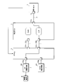
- FIG. 1 is a block diagram showing a network configuration of an in-vehicle communication system according to Embodiment 1;
- FIG. It is a block diagram which shows the structural example of 1ECU.
- It is a block diagram which shows the structural example of 2ECU.
- It is a block diagram which shows the structural example of FPGA.
- FIG. 4 is a block diagram showing a first example of connection path change; 4 is a flow chart showing procedures of route change processing and device control processing;
- FIG. 11 is a block diagram showing a second example of changing the connection path;
- FIG. 11 is a block diagram showing a third example of connection route change;
- FIG. 7 is a block diagram showing a network configuration of an in-vehicle communication system according to Embodiment 2;
- An object of the present disclosure is to provide an in-vehicle communication system, an in-vehicle control device, and a communication method that can cope with changes or expansion of in-vehicle equipment installed in a vehicle without changing the hardware configuration of the in-vehicle control device. It is in.
- an in-vehicle communication system an in-vehicle control device, and a communication method that can cope with changes or expansion of in-vehicle equipment installed in a vehicle without changing the hardware configuration of the in-vehicle control device. can be done.
- An in-vehicle communication system is an in-vehicle communication system including a first in-vehicle control device and a second in-vehicle control device that transmit control signals for controlling operations of in-vehicle devices,
- the second vehicle-mounted control device receives the control signal transmitted from the first vehicle-mounted control device, and outputs the received control signal as control data according to one of a plurality of types of communication protocols.
- a port further comprising: a plurality of first terminals to which the control data output from the plurality of ports are input; and a plurality of second terminals for outputting the control data, the plurality of first terminals;
- An FPGA Field Programmable Gate Array
- An FPGA Field Programmable Gate Array having a circuit capable of changing a connection path with the plurality of second terminals, and a control output from the plurality of second terminals, which are respectively connected to the plurality of second terminals.
- a plurality of communication circuits for converting data into a control signal conforming to one of the plurality of types of communication protocols and outputting the control signal to the vehicle-mounted device.
- the connection path from the port of the second vehicle-mounted control device to the communication circuit can be changed, and the second vehicle-mounted control device communicates with the vehicle-mounted device. Circuit can be changed.
- the first in-vehicle control device includes a circuit data output unit that outputs circuit data for changing the connection path to the FPGA, and the FPGA outputs the circuit data according to the circuit data output from the circuit data output unit.
- a configuration is preferable in which connection paths between the plurality of first terminals and the plurality of second terminals are changed.
- the second vehicle-mounted control device can change the communication circuit for communicating with the vehicle-mounted device.
- the plurality of first terminals include terminals to which digital data not conforming to the plurality of types of communication protocols output from the first vehicle-mounted control device are input, and the plurality of second terminals are configured to receive the It is preferable that the configuration includes an output circuit that includes a terminal for outputting digital data, is connected to the terminal for outputting the digital data, converts the digital data output from the terminal into an analog signal, and outputs the analog signal to the outside.
- the plurality of second terminals include terminals to which digital data not conforming to the plurality of types of communication protocols are input; the plurality of first terminals include terminals for outputting the digital data; It is preferable to include an input circuit connected to the terminal to which the digital data is input, converts an externally input analog signal into digital data, and outputs the digital data to the terminal.
- a second FPGA comprising a plurality of connector terminals and a third terminal connected to the communication circuit, and having a circuit capable of changing a connection path between the plurality of connector terminals and the third terminal; A configuration with such is preferred.
- the FPGA includes a plurality of connector terminals and a third terminal connected to the communication circuit, and has a circuit capable of changing a connection path between the plurality of connector terminals and the third terminal. is preferred.
- a second FPGA comprising a plurality of connector terminals and a third terminal connected to the output circuit, and having a circuit capable of changing a connection path between the plurality of connector terminals and the third terminal. A configuration with such is preferred.
- the FPGA includes a plurality of connector terminals and a third terminal connected to the output circuit, and has a circuit capable of changing a connection path between the plurality of connector terminals and the third terminal. is preferred.
- a second FPGA comprising a plurality of connector terminals and a third terminal connected to the input circuit, and having a circuit capable of changing a connection path between the plurality of connector terminals and the third terminal. A configuration with such is preferred.
- the FPGA includes a plurality of connector terminals and a third terminal connected to the input circuit, and has a circuit capable of changing a connection path between the plurality of connector terminals and the third terminal. is preferred.
- An in-vehicle control device receives a control signal for controlling the operation of an in-vehicle device, converts the received control signal to control data conforming to one of a plurality of types of communication protocols and a plurality of first terminals for inputting the control data output from the plurality of ports, and a plurality of second terminals for outputting the control data.
- An FPGA Field Programmable Gate Array having a circuit capable of changing a connection path between the plurality of first terminals and the plurality of second terminals, and an FPGA (Field Programmable Gate Array) that is connected to the plurality of second terminals, and a plurality of communication circuits for converting control data output from a plurality of second terminals into a control signal conforming to one of the plurality of types of communication protocols and outputting the control signal to the vehicle-mounted device.
- FPGA Field Programmable Gate Array
- a communication method receives a control signal for controlling the operation of an in-vehicle device, and converts the received control signal into control data conforming to one of a plurality of types of communication protocols.
- an FPGA Field Programmable Gate Array
- an FPGA field programmable gate array
- FIG. 1 is a block diagram showing a network configuration of an in-vehicle communication system according to Embodiment 1.
- FIG. The in-vehicle communication system according to the first embodiment includes a 1ECU (first in-vehicle control device) 1 and a 2ECU (second in-vehicle control device) 2 that transmit control signals for controlling the operation of the in-vehicle device B, and an FPGA 3 (Field Programmable Gate Array).
- the connector 1a of the 1ECU1 and the connector 21a of the 2ECU2 are connected by a communication line A.
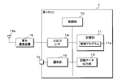
- FIG. 2 is a block diagram showing a configuration example of the first ECU1.
- the first ECU1 includes a control unit 10, a storage unit 11, a communication unit 12, a circuit data output unit 13, and an input/output I/F14.
- the storage unit 11 is a non-volatile memory device such as flash memory or EEPROM (Electrically Erasable Programmable Read Only Memory).
- the storage unit 11 stores a control program 11a necessary for controlling the in-vehicle device B.
- the in-vehicle device B is various sensors such as an in-vehicle camera that captures an image of the outside of the vehicle, a LIDAR (Light Detection And Ranging), and an in-vehicle camera.
- the in-vehicle device B is an actuator for operating a door locking/unlocking device, a door mirror, a seat, and the like.
- the in-vehicle device B may be an audio device that outputs entertainment images and sounds.
- the in-vehicle device B may be an electronic control unit.
- the control program 11a may be written in the storage unit 11 at the manufacturing stage of the first ECU1, or the control program distributed from an external server device (not shown) may be acquired by the first ECU1 and written in the storage unit 11. It may be an aspect.
- the first ECU 1 may read out the control program recorded in a computer-readable recording medium such as a memory card or an optical disc and write it in the storage unit 11 .
- the control program providing method may be provided in the form of distribution via a network, or may be provided in the form of being recorded on a recording medium.
- the control unit 10 is configured using an arithmetic processing device such as a CPU (Central Processing Unit) or MPU (Micro-Processing Unit), for example, and reads and executes a control program 11a or the like stored in the storage unit 11, Data for controlling the in-vehicle device B is generated.
- the control unit 10 has a function of converting the generated data into control data conforming to any of a plurality of communication protocols such as Ethernet (registered trademark), CAN, LIN, FlexRay (registered trademark), CXPI, etc.
- the control data converted so as to comply with the communication protocol is given to the communication unit 12 .
- the communication unit 12 is, for example, a communication circuit that converts control data given from the control unit 10 into a control signal conforming to a predetermined communication protocol, and transmits the converted control signal to the second ECU2.
- the communication unit 12 is connected to the second ECU 2 via the connector 1a and the communication line A.
- the communication circuit is, for example, an Ethernet (registered trademark) PHY unit that performs communication based on a communication protocol such as 100BASE-T1 or 1000BASE-T1. Note that Ethernet (registered trademark) is an example, and the communication unit 12 communicates with communication protocols such as CAN (Controller Area Network), CAN-FD, FlexRay, CXPI (Clock Extension Peripheral Interface), and LIN (Local Interconnect Network). may be a communication circuit that performs
- the input/output I/F 14 is an interface for communicating with the external communication device 15 and the like.
- the external communication device 15 is connected to the input/output I/F 14 via a wire harness such as a serial cable.
- the outside communication device 15 includes an antenna 15a for wireless communication, and performs wireless communication through an Internet communication network such as WiFi (registered trademark), a mobile communication network such as 3G, LTE (registered trademark), 4G, 5G, etc. It is a device.
- the external communication device 15 is, for example, a telematics control unit (TCU).
- the control unit 10 can receive the updated control program 11a, the circuit data for rewriting the circuit of the FPGA 3, and the like through the external communication device 15.
- FIG. In the first embodiment, the external communication device 15 and the 1ECU1 are described as separate bodies, but the 1ECU1 may be configured to have the configuration and function of the external communication device 15.
- the circuit data output unit 13 is a circuit that is connected to the FPGA3 and outputs circuit data for rewriting the circuit configuration of the FPGA3.
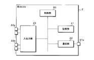
- FIG. 3 is a block diagram showing a configuration example of the second ECU2.
- the 2ECU2 has the same configuration as the 1ECU1, and includes a control unit 20, a storage unit 21, a communication unit 22 and an input/output unit 23.
- the storage unit 21 is a non-volatile memory device such as flash memory or EEPROM.
- the storage unit 21 controls the control signal transmitted from the second ECU 2 as control data according to one of a plurality of communication protocols such as Ethernet (registered trademark), CAN, LIN, FlexRay, CXPI, etc. Control the process of outputting to the FPGA 3 A program (not shown) to be executed by the unit 20 is stored.
- the communication unit 22 is a communication circuit that receives a control signal transmitted from the first ECU 1 and converts it into control data that the control unit 20 can process.
- the communication unit 22 is connected to the first ECU1 via the connector 21a and the communication line A.
- the communication circuit is, for example, an Ethernet (registered trademark) PHY unit that performs communication based on a communication protocol such as 100BASE-T1 or 1000BASE-T1. Note that Ethernet (registered trademark) is an example, and the communication unit 12 may be a communication circuit that performs communication using a communication protocol such as CAN, CAN-FD, FlexRay, CXPI, or LIN.
- the input/output unit 23 includes a plurality of input/output ports 22a..., 22b... that output at least control data to the FPGA3.
- input/output port 22a..., 22b... can also input the data output from FPGA3 to 2ECU2.
- the control unit 20 converts the control data obtained by the communication unit 22 receiving the control signal into control data conforming to one of a plurality of communication protocols such as Ethernet (registered trademark), CAN, LIN, FlexRay, and CXPI. It has the function to In FIG. 1, rounded rectangles "CAN” and “LIN”, and “CXPI” shown in FIG. , and the control unit 20 implements the function unit by executing a program stored in the storage unit 21 .
- the control unit 20 may have a function of converting into control data conforming to communication protocols such as Ethernet (registered trademark) and FlexRay.
- the control unit 20 executes a process of outputting the control data converted so as to comply with a predetermined communication protocol to the FPGA 3 through any one of the plurality of input/output ports 22a, 22b.
- the FPGA 3 is a circuit capable of rewriting the connection paths between the plurality of first terminals 31a, 31b, . . . and the plurality of second terminals 32a, 32b, .
- a CAN communication circuit 41 is connected to the second terminal 32a, and a LIN communication circuit 42 is connected to the second terminal 32b.
- the CAN communication circuit 41 is a circuit that converts the control data output from the second ECU 2 via the FPGA 3 into a control signal conforming to the CAN communication protocol and outputs the control signal to the in-vehicle device B.
- the LIN communication circuit 42 is a circuit that converts the control data output from the second ECU 2 via the FPGA 3 into a control signal conforming to the LIN communication protocol and outputs the control signal to the vehicle-mounted device B.
- FIG. 1 shows a set of CAN communication circuit 41, first terminal 31a, second terminal 32a, and input/output port 22a. , a plurality of sets of CAN communication circuits 41, 41, . . . , first terminals 31a, 31a, .
- FIG. 1 shows one set of LIN communication circuit 42, first terminal 31b, second terminal 32b, and input/output port 22b.
- FIG. 1 shows a CAN communication circuit 41 and a LIN communication circuit 42 as examples of communication circuits. may be provided. The greater the number and types of communication circuits connected to the FPGA 3, the more flexible the change and expansion of the in-vehicle device B mounted on the vehicle.
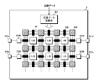
- FIG. 4 is a block diagram showing a configuration example of the FPGA3.
- the FPGA 3 includes a plurality of logic blocks LB arranged in a grid pattern, wiring W arranged vertically and horizontally so as to surround each logic block LB, switch blocks SB, connection blocks CB, and input/output ports for data input/output. block IOB.
- the logic block LB is a circuit that includes, for example, a LUT (Lookup table) and performs logic operations.
- the switch block SB is provided at an intersection of the wirings W and includes a transistor that turns on and off the connection path of the wirings W.
- the connection block CB is provided between the logic block LB and the wiring W, and includes a transistor that turns the connection between the logic block LB and the wiring W on and off.
- connection block CB is provided between the input/output block IOB and the wiring W, and includes a transistor for turning on/off the connection between the input/output block IOB and the wiring W.
- FIG. The input/output block IOB is connected to first terminals 31b, 31b, . . . and second terminals 32b, 32b, .
- the FPGA 3 can rewrite the circuit configuration by turning on and off the transistors that constitute the LUT of the logic block LB, the switch block SB and the connection block CB.
- the FPGA 3 includes a non-volatile circuit data storage section 30 that stores circuit data that defines the circuit configuration.
- the FPGA 3 can configure a specific circuit by reading the circuit data stored in the circuit data storage unit 30 and controlling the transistors that configure the LUT of the logic block LB, the switch block SB, and the connection block CB.
- the FPGA 3 according to the first embodiment can change the connection paths between the first terminals 31b, 31b, . . . and the second terminals 32b, 32b, .
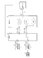
- FIG. 5 is a block diagram showing a first example of connection route change.
- the first terminal 31a and the second terminal 32a of the FPGA 3 are connected, and the 2ECU 2 is in a state of being connected to the CAN communication circuit 41 via the FPGA 3.
- the second 2ECU2 can output CAN control signals to the in-vehicle device B by outputting control data conforming to the CAN communication protocol from the input/output port 22a to the FPGA3.
- the first ECU1 can rewrite the circuit data stored in the circuit data storage unit 30 of the FPGA3 by outputting the circuit data to the FPGA3. For example, by rewriting the circuit data of the FPGA 3, the first ECU 1 cuts the path between the first terminal 31a and the second terminal 32a, and connects the first terminal 31b and the second terminal 32b, as shown in FIG. , and the second terminals 32b, 32b, . . . can be changed.
- the first terminal 31b and the second terminal 32b of the FPGA3 are connected, and the 2ECU2 is connected to the LIN communication circuit 42 via the FPGA3.
- the second 2ECU2 can output the LIN control signal to the in-vehicle device B by outputting the control data conforming to the LIN communication protocol from the input/output port 22b to the FPGA3.
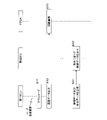
- FIG. 6 is a flow chart showing the procedure of route change processing and device control processing.
- the first ECU 1 downloads an update program for changing the hardware (step S11).
- the update program includes circuit data for rewriting the FPGA3. Further, the update program includes a program for executing processing for transmitting control data to the vehicle-mounted device B newly connected to the LIN communication circuit 42 .
- the control unit 10 of the first ECU 1 outputs circuit data to the FPGA 3 in order to rewrite the FPGA 3 (step S12).
- the FPGA 3 stores the circuit data output from the first ECU 1 in the circuit data storage unit 30, thereby rewriting the circuit configuration, that is, the connection paths between the first terminals 31b, 31b, . . . and the second terminals 32b, 32b, . (Step S13). For example, the connection path shown in FIG. 1 is changed to the connection path shown in FIG.
- the 1ECU1 transmits control data and instruction data to the 2ECU2 (step S31).
- the control data is data for controlling the operation of the in-vehicle device B.
- the instruction data includes port designation data indicating the input/output ports 22a . . . , 22b .
- the second 2ECU2 receives the control data and instruction data transmitted from the first 1ECU1, converts the received control data into control data conforming to the communication protocol specified by the protocol specification data, and specifies the port for the converted control data. Output to the input/output ports 22a, 22b, etc. indicated by the data (step S32).
- control data conforming to the LIN communication protocol is output from the input/output port 22b to the FPGA3.
- the control data output from the input/output port 22b is input to the first terminal 31b of the FPGA 3 and output to the LIN communication circuit 42 from the second terminal 32b.
- the LIN communication circuit 42 converts the control data output from the terminal 32b into a control signal conforming to the LIN communication protocol, and outputs the control signal to the in-vehicle device B.
- the in-vehicle device B connected via the FPGA 3 is changed, there is no need to change the hardware configuration of the 2ECU2. Further, there is no need to change the program of the second ECU2 for controlling the on-vehicle device B.
- the second 2ECU 2 only outputs the control data transmitted from the 1ECU from the specified input/output port 22b according to the specified communication protocol according to the instruction data, and the processing content changes before and after the connection path is changed. do not have. In this way, it is possible to cope with changes and additions of the in-vehicle device B only by rewriting the circuit of the FPGA 3 and changing the content of the instruction data transmitted by the first ECU 1 together with the control data.
- FIG. 7 is a block diagram showing a second example of connection route change.
- the communication circuit connected to the FPGA3 even if the communication circuit connected to the FPGA3 is changed, it can be dealt with only by changing the circuit of the FPGA3.
- the CAN communication circuit 41 connected to the second terminal 32a is changed to the LIN communication circuit 42
- the LIN communication circuit 42 connected to the second terminal 32b is changed to
- the hardware is changed by disconnecting the path between the first terminal 31b and the second terminal 32b and connecting the path between the first terminal 31b and the second terminal 32a. can be absorbed. That is, it is possible to control the LIN communication circuit 42 and the in-vehicle device B that have been rearranged without changing the hardware and software of the 1ECU1 and the 2ECU2.
- FIG. 8 is a block diagram showing a third example of connection route change.
- the on-vehicle device B connected to the LIN communication circuit 42 in FIG. 7 is changed to connect to the CXPI communication circuit 43
- the first terminal 31b and the second terminal Hardware change can be absorbed by cutting off the path to 32a and connecting the path to the first terminal 31b and the second terminal 32b. That is, there is no need to change the hardware of the first 1ECU1 and the second 2ECU2, and only by changing the circuit configuration of the FPGA3, the LIN communication circuit 42 and the in-vehicle device B that have been rearranged can be controlled.
- the communication circuit for the 2ECU2 to communicate with the in-vehicle device B can be changed.
- the in-vehicle communication system and communication method according to the second embodiment differs from the first embodiment in that the hardware can be changed to enable input/output of any analog signal to/from the in-vehicle device B.
- FIG. Since other configurations are the same as those of the in-vehicle communication system according to the first embodiment, etc., the same parts are denoted by the same reference numerals, and detailed description thereof will be omitted.
- 9 and 10 are block diagrams showing the network configuration of the in-vehicle communication system according to the second embodiment.
- the second 2ECU 2 includes input/output ports 22c and 22d for inputting and outputting digital data that does not conform to a communication protocol such as CAN.
- the digital data is, for example, digital data obtained by AD conversion, DA conversion, filter processing, or the like of an analog signal input/output to/from the in-vehicle device B.
- FPGA3 has the same configuration as the first embodiment, is further connected to the input/output ports 22c and 22d of the second 2ECU2, the first terminal for inputting and outputting digital data that does not conform to a communication protocol such as CAN 31c and 31d.
- the FPGA 3 also has second terminals 32 c and 31 d connected to the I/O circuits 45 and 46 .
- the I/O circuits 45 and 46 are circuits for inputting and outputting analog signals by converting digital data into analog signals and converting analog signals into digital signals.
- the first I/O circuit 45 is a circuit that converts the digital data output from the second terminal 32c into an analog signal and outputs the analog signal to the in-vehicle device B.
- a circuit 46 converts an analog signal output from the vehicle-mounted device B into digital data and outputs the digital data to the second terminal 32d.
- the 1ECU transmits a control signal including digital data and instruction data for generating an analog signal to be output to the vehicle-mounted device B to the 2ECU2.
- the instruction data includes port designation data indicating the input/output ports 22a, 22b, . . . to output analog data.
- the 2ECU receives the control signal transmitted from the 1ECU1, filters the digital data contained in the received control signal, and transmits the filtered digital data to the FPGA 3 from the input/output port 22d indicated by the port designation data. Output to the first terminal 31d.
- the digital data output from 2ECU2 is output to the I/O circuit 45 via the 1st terminal 31d and the 2nd terminal 32c, and is output to the vehicle equipment B from the I/O circuit 45 as an analog signal.
- the first ECU1 can rewrite the circuit configuration of the FPGA3 by outputting circuit data to the FPGA3. For example, as shown in FIGS. 9 and 10, the path between the first terminal 31d and the second terminal 32c can be blocked and the first terminal 31d and the second terminal 32d can be connected.
- the circuit configuration is changed as shown in FIG. 10, the analog signal output from the in-vehicle device B is converted into digital data by the I/O circuit 46, and the digital data is transmitted through the second terminal 32d and the first terminal 31d. It is configured to be input to the input/output port 22d via.
- the second 2ECU2 performs input filter processing on the input digital data, and transmits the input filtered data to the first 1ECU1.
- FIG. 11 is a flow chart showing the procedure of route change processing and device control processing.
- the first ECU 1 downloads an update program for changing the hardware (step S51).
- the update program includes circuit data for rewriting the FPGA3. Further, the update program includes a program for processing a digital signal output from the newly connected vehicle-mounted device B.
- the control unit 10 of the first ECU 1 outputs circuit data to the FPGA 3 in order to rewrite the FPGA 3 (step S52).
- the FPGA 3 stores the circuit data output from the first ECU 1 in the circuit data storage unit 30, thereby rewriting the circuit configuration, that is, the connection paths between the first terminals 31b, 31b, . . . and the second terminals 32b, 32b, . (Step S53). For example, the connection path shown in FIG. 9 is changed to the connection path shown in FIG.
- control unit 10 of the 1ECU1 transmits to the 2ECU2 filter designation data that designates a change in the content of the input filter processing for the digital data from the newly connected vehicle-mounted device B (step S54).
- the second 2ECU2 receives the filter designation data transmitted from the first 1ECU1, and uses the filter designated by the received filter designation data to perform the input processing of the digital data input from the in-vehicle device B Input processing content is changed (step S55).
- the circuit configuration of the FPGA3 is changed, and only the content of the filter processing in the second 2ECU2 is changed. , it is possible to cope with changes and additions of such in-vehicle device B.
- the FPGA3 may be configured to execute the filtering process.
- the filter circuit may be configured in the FPGA 3 by changing the circuit data.
- the in-vehicle communication system and communication method according to the third embodiment differs from the second embodiment in that the connector terminal for connecting to the in-vehicle device B can be changed by rewriting the FPGA3. Since other configurations are the same as those of the in-vehicle communication system according to the second embodiment, etc., similar portions are denoted by the same reference numerals, and detailed description thereof will be omitted.
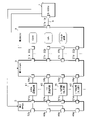
- FIG. 12 is a block diagram showing the network configuration of the in-vehicle communication system according to the third embodiment.
- the in-vehicle communication system according to Embodiment 3 includes a first FPGA3 and a second FPGA5. Since the first FPGA 3 has the same configuration as the FPGA 3 of Embodiments 1 and 2, the same reference numerals are given and the details are omitted.
- 2nd FPGA5 is a circuit for switching the connector terminal for connecting with the vehicle equipment B.
- the second FPGA 5 includes a CAN communication circuit 41, a LIN communication circuit 42, an I/O circuit 45, a plurality of third terminals 51a, 51b, 51c, and 51d connected to the terminals of the I/O circuit 45 on the in-vehicle device B side, A plurality of connector terminals 52a, 52b, 52c and 52d are provided.
- FIG. 12 shows four sets of third terminals 51a, 51b, 51c, 51d and connector terminals 52a, 52b, 52c, 52d, the numbers of terminals and connectors are not particularly limited. . Also, they do not have to be the same number.
- the circuit configuration of the second FPGA 5 is the same as that of the first FPGA 3, and by rewriting the circuit data, the connection paths between the plurality of third terminals 51a, 51b, 51c and 51d and the plurality of connector terminals 52a, 52b, 52c and 52d are changed. can be changed.
- the CAN communication circuit 41 is connected to the connector terminal 52a via the third terminal 51a, and the LIN communication circuit 42 is connected to the connector terminal 52c via the third terminal 51b.
- the first ECU1 when it is desired to change the hardware configuration so that the CAN control signal is input/output using the connector terminal 52b, the first ECU1 outputs the circuit data to the second FPGA 5 to change the circuit configuration, so that the third This can be handled by connecting the terminal 51a and the connector terminal 52b.
- the CAN communication circuit 41, the LIN communication circuit 42, the I/O circuit 45, and the I/O circuit 46 connector terminals 52a, 52b, 52c, 52d is changed, the connector terminals 52a, 52b, 52c, and 52d for inputting and outputting various control signals and analog signals can be changed only by changing the circuit configuration of the second FPGA 5. Changes and additions can be accommodated.
- the in-vehicle communication system and communication method according to the fourth embodiment differs from the second embodiment in that the connector terminal for connecting to the in-vehicle device B can be changed by rewriting the FPGA3. Since other configurations are the same as those of the in-vehicle communication system according to the second embodiment, etc., similar portions are denoted by the same reference numerals, and detailed description thereof will be omitted.
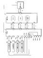
- FIG. 13 is a block diagram showing the network configuration of the in-vehicle communication system according to the fourth embodiment.
- the FPGA 3 according to the fourth embodiment includes a plurality of third terminals 33a, 33b, and 33c connected to terminals of the CAN communication circuit 41, the LIN communication circuit 42, the I/O circuit 45, and the I/O circuit 46 on the in-vehicle device B side. , 33d and a plurality of connector terminals 34a, 34b, 34c, 34d.
- FIG. 13 shows four sets of third terminals 33a, 33b, 33c and 33d and connector terminals 34a, 34b, 34c and 34d, the numbers of terminals and connectors are not particularly limited. . Also, they do not have to be the same number.
- the circuit configuration of the FPGA3 is the same as that of the FPGA3, and by rewriting the circuit data, the connection paths between the plurality of third terminals 33a, 33b, 33c, and 33d and the plurality of connector terminals 34a, 34b, 34c, and 34d are changed. be able to.
- the CAN communication circuit 41 is connected to the connector terminal 34c via the third terminal 33c, and the LIN communication circuit 42 is connected to the connector terminal 34a via the third terminal 33d.
- the first ECU1 when it is desired to change the hardware configuration so that the CAN control signal is input/output using the connector terminal 34b, the first ECU1 outputs the circuit data to the FPGA3 to change the circuit configuration, so that the third terminal 33d and the connector terminal 34b can be connected.
- the connector terminals of the CAN communication circuit 41, the LIN communication circuit 42, the I/O circuit 45, and the I/O circuit 46 to which the in-vehicle device B is connected are connected. Even if 52a, 52b, 52c and 52d are changed, only by changing the circuit configuration of FPGA 3, connector terminals 52a, 52b, 52c and 52d for inputting and outputting various control signals and analog signals can be changed, Changes and additions to the in-vehicle device B can be accommodated.
- the FPGA 3 may be arranged inside the housing of the 2ECU 2.
- the wiring connecting the 1ECU1 and the FPGA3 may pass through the 2ECU2.
- the first ECU1 may be configured to transmit the circuit data to the FPGA3 using the communication line A and rewrite the circuit data.
- Embodiments 1 to 4 the example in which the first ECU 1 rewrites the circuit data of the FPGA 3 has been described, but the configuration is such that the circuit data of the FPGA 3 is rewritten using another in-vehicle device or an external device such as a diagnostic tool. You may In addition, in the assembly process of the vehicle before shipping from the factory, when changing the connection mode to the in-vehicle equipment installed according to the difference in the vehicle type, the presence or absence of options, etc., the circuit using an arbitrary external computer An FPGA 3 with rewritten data may be mounted.
Landscapes
- Engineering & Computer Science (AREA)
- Theoretical Computer Science (AREA)
- Physics & Mathematics (AREA)
- Computer Hardware Design (AREA)
- General Physics & Mathematics (AREA)
- Mechanical Engineering (AREA)
- General Engineering & Computer Science (AREA)
- Computer Networks & Wireless Communication (AREA)
- Signal Processing (AREA)
- Mathematical Physics (AREA)
- Software Systems (AREA)
- Communication Control (AREA)
- Multi Processors (AREA)
- Small-Scale Networks (AREA)
Abstract
制御信号を送信する第1及び第2車載制御装置を備えた車載通信システムであって、第2車載制御装置は、第1車載制御装置から送信された制御信号を、複数種類の通信プロトコルのいずれかに準じた制御データとして出力する複数のポートを備え、更に、複数のポートから出力された制御データが入力する複数の第1端子と、制御データを出力する複数の第2端子とを備え、複数の第1及び第2端子間の接続経路を書き換え可能なFPGAと、複数の第2端子から出力された制御データを、複数種類の通信プロトコルのいずれかに準じた制御信号に変換して車載機器へ出力する複数の通信回路とを備える。
Description
本開示は、車載通信システム、車載制御装置及び通信方法に関する。
本出願は、2021年1月22日出願の日本出願第2021-008819号に基づく優先権を主張し、前記日本出願に記載された全ての記載内容を援用するものである。
本出願は、2021年1月22日出願の日本出願第2021-008819号に基づく優先権を主張し、前記日本出願に記載された全ての記載内容を援用するものである。
車両には、車載ネットワークに接続された複数の電子制御ユニット(ECU:Electronic Control Unit)が搭載されている。以下、電子制御ユニットをECU又は車載制御装置と呼ぶ。
本開示の一態様に係る車載通信システムは、車載機器の動作を制御するための制御信号を送信する第1車載制御装置及び第2車載制御装置を備えた車載通信システムであって、前記第2車載制御装置は、前記第1車載制御装置から送信された前記制御信号を受信し、受信した前記制御信号を、複数種類の通信プロトコルのいずれかに準じた制御データとして出力する複数のポートを備え、更に、前記複数のポートから出力された前記制御データが入力する複数の第1端子と、前記制御データを出力する複数の第2端子とを備え、前記複数の第1端子と、前記複数の第2端子との接続経路を変更可能な回路を有するFPGA(Field Programmable Gate Array)と、前記複数の第2端子にそれぞれ接続されており、前記複数の第2端子から出力された制御データを、前記複数種類の通信プロトコルのいずれかに準じた制御信号に変換して前記車載機器へ出力する複数の通信回路とを備える。
本開示の一態様に係る車載制御装置は、車載機器の動作を制御するための制御信号を受信し、受信した前記制御信号を、複数種類の通信プロトコルのいずれかに準じた制御データとして出力する複数のポートを備えた車載制御装置であって、前記複数のポートから出力された前記制御データが入力する複数の第1端子と、前記制御データを出力する複数の第2端子とを備え、前記複数の第1端子と、前記複数の第2端子との接続経路を変更可能な回路を有するFPGA(Field Programmable Gate Array)と、前記複数の第2端子にそれぞれ接続されており、前記複数の第2端子から出力された制御データを、前記複数種類の通信プロトコルのいずれかに準じた制御信号に変換して前記車載機器へ出力する複数の通信回路とを備える。
本開示の一態様に係る通信方法は、車載機器の動作を制御するための制御信号を受信し、受信した前記制御信号を、複数種類の通信プロトコルのいずれかに準じた制御データとして出力する複数のポートを備えた車載制御装置を用いた通信方法であって、前記複数のポートから出力された前記制御データが入力する複数の第1端子と、前記制御データを出力する複数の第2端子とを備え、前記複数の第1端子と、前記複数の第2端子との接続経路を変更可能な回路を有するFPGA(Field Programmable Gate Array)と、前記複数の第2端子にそれぞれ接続されており、前記複数の第2端子から出力された制御データを、前記複数種類の通信プロトコルのいずれかに準じた制御信号に変換して前記車載機器へ出力する複数の通信回路とを用意し、前記FPGAにおける接続経路を変更することによって、前記車載制御装置の前記ポートに接続される前記通信回路を切り替える。
なお、本願は、このような特徴的なプロセッサを備える車載コンピュータとして実現することができるだけでなく、上記の通り、かかる特徴的な処理をステップとするコンピュータ実行方法として実現したり、かかるステップをコンピュータに実行させるためのコンピュータプログラムとして実現したりすることができる。また、車載コンピュータの一部又は全部を実現する半導体集積回路として実現したり、車載コンピュータを含むその他のシステムとして実現したりすることができる。
[本開示が解決しようとする課題]
本開示の目的は、車載制御装置のハードウェア構成を変更すること無く、車両に搭載される車載機器の変更又は拡充に対応することができる車載通信システム、車載制御装置及び通信方法を提供することにある。
本開示の目的は、車載制御装置のハードウェア構成を変更すること無く、車両に搭載される車載機器の変更又は拡充に対応することができる車載通信システム、車載制御装置及び通信方法を提供することにある。
[本開示の効果]
本開示によれば、車載制御装置のハードウェア構成を変更すること無く、車両に搭載される車載機器の変更又は拡充に対応することができる車載通信システム、車載制御装置及び通信方法を提供することができる。
本開示によれば、車載制御装置のハードウェア構成を変更すること無く、車両に搭載される車載機器の変更又は拡充に対応することができる車載通信システム、車載制御装置及び通信方法を提供することができる。
[本開示の実施形態の説明]
最初に本開示の実施態様を列記して説明する。また、以下に記載する実施形態の少なくとも一部を任意に組み合わせてもよい。
最初に本開示の実施態様を列記して説明する。また、以下に記載する実施形態の少なくとも一部を任意に組み合わせてもよい。
(1)本開示の一態様に係る車載通信システムは、車載機器の動作を制御するための制御信号を送信する第1車載制御装置及び第2車載制御装置を備えた車載通信システムであって、前記第2車載制御装置は、前記第1車載制御装置から送信された前記制御信号を受信し、受信した前記制御信号を、複数種類の通信プロトコルのいずれかに準じた制御データとして出力する複数のポートを備え、更に、前記複数のポートから出力された前記制御データが入力する複数の第1端子と、前記制御データを出力する複数の第2端子とを備え、前記複数の第1端子と、前記複数の第2端子との接続経路を変更可能な回路を有するFPGA(Field Programmable Gate Array)と、前記複数の第2端子にそれぞれ接続されており、前記複数の第2端子から出力された制御データを、前記複数種類の通信プロトコルのいずれかに準じた制御信号に変換して前記車載機器へ出力する複数の通信回路とを備える。
本態様によれば、FPGAの回路構成を書き換えることによって、第2車載制御装置のポートから通信回路への接続経路を変更することができ、第2車載制御装置が車載機器と通信するための通信回路を変更することができる。
(2)第1車載制御装置は、前記接続経路を変更するための回路データを前記FPGAへ出力する回路データ出力部を備え、前記FPGAは、前記回路データ出力部から出力された前記回路データに従って前記複数の第1端子と、前記複数の第2端子との接続経路を変更する構成が好ましい。
本態様によれば、第1車載制御装置からFPGAへ回路データを出力して、FPGAの回路構成を書き換えることによって、第2車載制御装置が車載機器と通信するための通信回路を変更することができる。
(3)前記複数の第1端子は、前記第1車載制御装置から出力された、前記複数種類の通信プロトコルに準拠しないデジタルデータが入力される端子を含み、前記複数の第2端子は、前記デジタルデータを出力する端子を含み、更に、前記デジタルデータを出力する端子に接続されており、該端子から出力されたデジタルデータをアナログ信号に変換して外部出力する出力回路を備える構成が好ましい。
本態様によれば、FPGAの回路構成を書き換えるのみで、第2車載制御装置から車載機器へアナログ信号を出力可能なハードウェア構成に変更することができる。
(4)前記複数の第2端子は、前記複数種類の通信プロトコルに準拠しないデジタルデータが入力される端子を含み、前記複数の第1端子は、前記デジタルデータを出力する端子を含み、更に、前記デジタルデータが入力される端子に接続されており、外部入力されたアナログ信号をデジタルデータに変換して該端子へ出力する入力回路を備える構成が好ましい。
本態様によれば、FPGAの回路構成を書き換えるのみで、車載機器から第2車載制御装置へアナログ信号を入力可能なハードウェア構成に変更することができる。
(5)複数のコネクタ端子と、前記通信回路に接続される第3端子とを備え、前記複数のコネクタ端子と、前記第3端子との接続経路を変更可能な回路を有する第2のFPGAを備える構成が好ましい。
本態様によれば、第2のFPGAの回路構成を書き換えるのみで、第2車載制御装置と、車載機器とを接続する通信回路のコネクタ端子を変更することができる。
(6)前記FPGAは、複数のコネクタ端子と、前記通信回路に接続される第3端子とを備え、前記複数のコネクタ端子と、前記第3端子との接続経路を変更可能な回路を有する構成が好ましい。
本態様によれば、FPGAの回路構成を書き換えるのみで、第2車載制御装置と、車載機器とを接続する通信回路のコネクタ端子を変更することができる。
(7)複数のコネクタ端子と、前記出力回路に接続される第3端子とを備え、前記複数のコネクタ端子と、前記第3端子との接続経路を変更可能な回路を有する第2のFPGAを備える構成が好ましい。
本態様によれば、第2のFPGAの回路構成を書き換えるのみで、第2車載制御装置と、車載機器とを接続する出力回路のコネクタ端子を変更することができる。
(8)前記FPGAは、複数のコネクタ端子と、前記出力回路に接続される第3端子とを備え、前記複数のコネクタ端子と、前記第3端子との接続経路を変更可能な回路を有する構成が好ましい。
本態様によれば、FPGAの回路構成を書き換えるのみで、第2車載制御装置と、車載機器とを接続する出力回路のコネクタ端子を変更することができる。
(9)複数のコネクタ端子と、前記入力回路に接続される第3端子とを備え、前記複数のコネクタ端子と、前記第3端子との接続経路を変更可能な回路を有する第2のFPGAを備える構成が好ましい。
本態様によれば、第2のFPGAの回路構成を書き換えるのみで、第2車載制御装置と、車載機器とを接続する入力回路のコネクタ端子を変更することができる。
(10)前記FPGAは、複数のコネクタ端子と、前記入力回路に接続される第3端子とを備え、前記複数のコネクタ端子と、前記第3端子との接続経路を変更可能な回路を有する構成が好ましい。
本態様によれば、FPGAの回路構成を書き換えるのみで、第2車載制御装置と、車載機器とを接続する入力回路のコネクタ端子を変更することができる。
(11)本開示の一態様に係る車載制御装置は、車載機器の動作を制御するための制御信号を受信し、受信した前記制御信号を、複数種類の通信プロトコルのいずれかに準じた制御データとして出力する複数のポートを備えた車載制御装置であって、前記複数のポートから出力された前記制御データが入力する複数の第1端子と、前記制御データを出力する複数の第2端子とを備え、前記複数の第1端子と、前記複数の第2端子との接続経路を変更可能な回路を有するFPGA(Field Programmable Gate Array)と、前記複数の第2端子にそれぞれ接続されており、前記複数の第2端子から出力された制御データを、前記複数種類の通信プロトコルのいずれかに準じた制御信号に変換して前記車載機器へ出力する複数の通信回路とを備える。
本態様によれば、態様(1)同様、FPGAの回路構成を書き換えることによって、第2車載制御装置のポートから通信回路への接続経路を変更することができ、第2車載制御装置が車載機器と通信するための通信回路を変更することができる。
(12)本開示の一態様に係る通信方法は、車載機器の動作を制御するための制御信号を受信し、受信した前記制御信号を、複数種類の通信プロトコルのいずれかに準じた制御データとして出力する複数のポートを備えた車載制御装置を用いた通信方法であって、前記複数のポートから出力された前記制御データが入力する複数の第1端子と、前記制御データを出力する複数の第2端子とを備え、前記複数の第1端子と、前記複数の第2端子との接続経路を変更可能な回路を有するFPGA(Field Programmable Gate Array)と、前記複数の第2端子にそれぞれ接続されており、前記複数の第2端子から出力された制御データを、前記複数種類の通信プロトコルのいずれかに準じた制御信号に変換して前記車載機器へ出力する複数の通信回路とを用意し、前記FPGAにおける接続経路を変更することによって、前記車載制御装置の前記ポートに接続される前記通信回路を切り替える。
本態様によれば、態様(1)同様、FPGAの回路構成を書き換えることによって、第2車載制御装置のポートから通信回路への接続経路を変更することができ、第2車載制御装置が車載機器と通信するための通信回路を変更することができる。
[本開示の実施形態の詳細]
本開示の実施形態に係る車載通信システム、車載制御装置及び通信方法を、以下に図面を参照しつつ説明する。なお、本発明はこれらの例示に限定されるものではなく、請求の範囲によって示され、請求の範囲と均等の意味及び範囲内でのすべての変更が含まれることが意図される。また、以下に記載する実施形態の少なくとも一部を任意に組み合わせてもよい。
本開示の実施形態に係る車載通信システム、車載制御装置及び通信方法を、以下に図面を参照しつつ説明する。なお、本発明はこれらの例示に限定されるものではなく、請求の範囲によって示され、請求の範囲と均等の意味及び範囲内でのすべての変更が含まれることが意図される。また、以下に記載する実施形態の少なくとも一部を任意に組み合わせてもよい。
以下、本開示をその実施形態を示す図面に基づいて具体的に説明する。
(実施形態1)
図1は、実施形態1に係る車載通信システムのネットワーク構成を示すブロック図である。本実施形態1に係る車載通信システムは、車載機器Bの動作を制御するための制御信号を送信する第1ECU(第1車載制御装置)1及び第2ECU(第2車載制御装置)2と、FPGA3(Field Programmable Gate Array)とを備える。第1ECU1のコネクタ1aと、第2ECU2のコネクタ21aとは通信線Aにて接続されている。
(実施形態1)
図1は、実施形態1に係る車載通信システムのネットワーク構成を示すブロック図である。本実施形態1に係る車載通信システムは、車載機器Bの動作を制御するための制御信号を送信する第1ECU(第1車載制御装置)1及び第2ECU(第2車載制御装置)2と、FPGA3(Field Programmable Gate Array)とを備える。第1ECU1のコネクタ1aと、第2ECU2のコネクタ21aとは通信線Aにて接続されている。
図2は、第1ECU1の構成例を示すブロック図である。第1ECU1は、制御部10、記憶部11、通信部12、回路データ出力部13と、入出力I/F14とを備える。
記憶部11は、フラッシュメモリ又はEEPROM(Electrically Erasable Programmable Read Only Memory)等の不揮発性のメモリ素子である。記憶部11は、車載機器Bを制御するために必要な制御プログラム11aを記憶する。車載機器Bは、車外を撮像する車載カメラ、LIDAR(Light Detection And Ranging)、車内カメラ等の各種センサである。また車載機器Bは、ドアの施解錠装置、ドアミラー、シート等を動作させるアクチュエータである。車載機器Bは、エンターテイメント系の画像、音声を出力するオーディオ装置であっても良い。車載機器Bは、電子制御ユニットであっても良い。
なお、制御プログラム11aは、第1ECU1の製造段階において記憶部11に書き込まれる態様でもよいし、外部サーバ装置(不図示)から配信された上記制御プログラムを第1ECU1が取得して記憶部11に書き込む態様であってもよい。また、メモリカード又は光ディスク等のコンピュータ読み取り可能な記録媒体に記録された上記制御プログラムを第1ECU1が読み出して記憶部11に書き込む態様であってもよい。上記制御プログラムの提供方法は、上記の通り、ネットワークを介した配信の態様で提供されてもよいし、記録媒体に記録された態様で提供されてもよい。
なお、制御プログラム11aは、第1ECU1の製造段階において記憶部11に書き込まれる態様でもよいし、外部サーバ装置(不図示)から配信された上記制御プログラムを第1ECU1が取得して記憶部11に書き込む態様であってもよい。また、メモリカード又は光ディスク等のコンピュータ読み取り可能な記録媒体に記録された上記制御プログラムを第1ECU1が読み出して記憶部11に書き込む態様であってもよい。上記制御プログラムの提供方法は、上記の通り、ネットワークを介した配信の態様で提供されてもよいし、記録媒体に記録された態様で提供されてもよい。
制御部10は、例えばCPU(Central Processing Unit)又はMPU(Micro-Processing Unit)等の演算処理装置を用いて構成され、記憶部11に記憶された制御プログラム11a等を読み出して実行することにより、車載機器Bを制御するためのデータを生成する。制御部10は、生成したデータをイーサネット(登録商標)、CAN、LIN、FlexRay(登録商標)、CXPI等の複数の通信プロトコルのいずれかに準じた制御データに変換する機能を有し、所定の通信プロトコルに準拠するように変換された制御データを通信部12に与える。
通信部12は、例えば、制御部10から与えられた制御データを所定の通信プロトコルに準拠した制御信号に変換し、変換した制御信号を第2ECU2へ送信する通信回路である。通信部12は、コネクタ1a及び通信線Aを介して第2ECU2に接続されている。当該通信回路は、例えば、100BASE-T1又は1000BASE-T1等の通信プロトコルに準拠して通信を行うイーサネット(登録商標)PHY部である。なお、イーサネット(登録商標)は一例であり、通信部12は、CAN(Controller Area Network)、CAN-FD、FlexRay、CXPI(Clock Extension Peripheral Interface)、LIN(Local Interconnect Network)等の通信プロトコルで通信を行う通信回路であってもよい。
入出力I/F14は、車外通信装置15等と通信するためのインタフェースである。車外通信装置15は、シリアルケーブル等のワイヤーハーネスを介して入出力I/F14に接続されている。
車外通信装置15は、無線通信を行うためのアンテナ15aを備え、WiFi(登録商標)等のインターネット通信ネットワーク、3G、LTE(登録商標)、4G、5G等のモバイル通信ネットワークを通じて無線通信を行う通信装置である。車外通信装置15は、例えばテレマティクス制御ユニット(TCU)である。制御部10は、車外通信装置15にて、更新された制御プログラム11a、FPGA3の回路を書き換えるための回路データ等を受信することができる。なお、本実施形態1は車外通信装置15と第1ECU1が別体であるものとして説明するが、第1ECU1が車外通信装置15の構成ないし機能を有するように構成しても良い。
回路データ出力部13は、FPGA3に接続されており、FPGA3の回路構成を書き換えるための回路データを出力する回路である。
図3は、第2ECU2の構成例を示すブロック図である。第2ECU2は、第1ECU1と同様の構成であり、制御部20、記憶部21、通信部22及び入出力部23を備える。
記憶部21は、フラッシュメモリ又はEEPROM等の不揮発性のメモリ素子である。記憶部21は、第2ECU2から送信された制御信号を、イーサネット(登録商標)、CAN、LIN、FlexRay、CXPI等の複数の通信プロトコルのいずれかに準じた制御データとしてFPGA3へ出力する処理を制御部20に実行させるためのプログラム(不図示)を記憶する。
通信部22は、第1ECU1から送信された制御信号を受信し、制御部20が処理できる制御データに変換する通信回路である。通信部22は、コネクタ21a及び通信線Aを介して第1ECU1に接続されている。当該通信回路は、例えば、100BASE-T1又は1000BASE-T1等の通信プロトコルに準拠して通信を行うイーサネット(登録商標)PHY部である。なお、イーサネット(登録商標)は一例であり、通信部12は、CAN、CAN-FD、FlexRay、CXPI、LIN等の通信プロトコルで通信を行う通信回路であってもよい。
入出力部23は、少なくとも制御データをFPGA3へ出力する複数の入出力ポート22a…,22b…を備える。なお、入出力ポート22a…,22b…は、FPGA3から第2ECU2へ出力されたデータを入力することもできる。
制御部20は、通信部22が制御信号を受信して得た制御データを、イーサネット(登録商標)、CAN、LIN、FlexRay、CXPI等の複数の通信プロトコルのいずれかに準じた制御データに変換する機能を有する。図1中、角丸長方形の「CAN」、「LIN」、図7に示す「CXPI」は、第1ECU1からの制御データをCAN、LIN、CXPI等に準拠した制御データに変換する機能部を示しており、制御部20は、記憶部21が記憶するプログラムを実行することによって、当該機能部を実現する。もちろん、制御部20は、イーサネット(登録商標)、FlexRay等の通信プロトコルに準拠した制御データに変換する機能を備えてもよい。制御部20は、所定の通信プロトコルに準拠するように変換された制御データを複数の入出力ポート22a…,22b…のいずれのポートを介してFPGA3へ出力する処理を実行する。
FPGA3は、図1に示すように、第2ECU2の複数の入出力ポート22a…,22b…から出力された制御データが入力する複数の第1端子31a…,31b…と、制御データを出力する複数の第2端子32a…,32b…とを備える。FPGA3は、複数の第1端子31a…,31b…と、複数の第2端子32a…,32b…との接続経路を書き換え可能な回路である。
第2端子32aにはCAN通信回路41が接続され、第2端子32bにはLIN通信回路42が接続されている。CAN通信回路41は、第2ECU2からFPGA3を介して出力された制御データを、CAN通信プロトコルに準拠した制御信号に変換して、車載機器Bへ出力する回路である。LIN通信回路42は、第2ECU2からFPGA3を介して出力された制御データを、LIN通信プロトコルに準拠した制御信号に変換して、車載機器Bへ出力する回路である。
なお、作図の便宜上、図1には、1組みのCAN通信回路41、第1端子31a、第2端子32a,入出力ポート22aを図示しているが、本実施形態1に係る車載通信システムは、複数組みのCAN通信回路41,41…、第1端子31a,31a…、第2端子32a,32a…,入出力ポート22a,22a…を備える。同様に図1には、1組みのLIN通信回路42、第1端子31b、第2端子32b,入出力ポート22bを図示しているが、本実施形態1に係る車載通信システムは、複数組みのLIN通信回路42,42…、第1端子31b,31b…、第2端子32b,32b…,入出力ポート22b,22b…を備える。
また、図1では、通信回路の一例として、CAN通信回路41及びLIN通信回路42を図示しているが、イーサネット(登録商標)PHY部、FlexRay、CXPI(Clock Extension Peripheral Interface)、その他の通信回路を備えてもよい。FPGA3に接続する通信回路の種類及び個数が多い程、車両に搭載される車載機器Bの変更及び拡充により柔軟に対応することが可能である。
第2端子32aにはCAN通信回路41が接続され、第2端子32bにはLIN通信回路42が接続されている。CAN通信回路41は、第2ECU2からFPGA3を介して出力された制御データを、CAN通信プロトコルに準拠した制御信号に変換して、車載機器Bへ出力する回路である。LIN通信回路42は、第2ECU2からFPGA3を介して出力された制御データを、LIN通信プロトコルに準拠した制御信号に変換して、車載機器Bへ出力する回路である。
なお、作図の便宜上、図1には、1組みのCAN通信回路41、第1端子31a、第2端子32a,入出力ポート22aを図示しているが、本実施形態1に係る車載通信システムは、複数組みのCAN通信回路41,41…、第1端子31a,31a…、第2端子32a,32a…,入出力ポート22a,22a…を備える。同様に図1には、1組みのLIN通信回路42、第1端子31b、第2端子32b,入出力ポート22bを図示しているが、本実施形態1に係る車載通信システムは、複数組みのLIN通信回路42,42…、第1端子31b,31b…、第2端子32b,32b…,入出力ポート22b,22b…を備える。
また、図1では、通信回路の一例として、CAN通信回路41及びLIN通信回路42を図示しているが、イーサネット(登録商標)PHY部、FlexRay、CXPI(Clock Extension Peripheral Interface)、その他の通信回路を備えてもよい。FPGA3に接続する通信回路の種類及び個数が多い程、車両に搭載される車載機器Bの変更及び拡充により柔軟に対応することが可能である。
図4は、FPGA3の構成例を示すブロック図である。FPGA3は、格子状に配された複数の論理ブロックLBと、各論理ブロックLBを囲むように縦横に配された配線Wと、スイッチブロックSBと、コネクションブロックCBと、データが入出力する入出力ブロックIOBとを備える。論理ブロックLBは、例えばLUT(Lookup table)を備え、論理演算を行う回路である。スイッチブロックSBは、配線Wの交点に設けられ、配線Wによる接続経路をオンオフするトランジスタを備える。コネクションブロックCBは、論理ブロックLBと、配線Wとの間に設けられ、論理ブロックLBと配線Wとの接続をオンオフするトランジスタを備える。また、コネクションブロックCBは、入出力ブロックIOBと、配線Wとの間に設けられ、入出力ブロックIOBと配線Wとの接続をオンオフするトランジスタを備える。入出力ブロックIOBは、第1端子31b,31b…、第2端子32b,32b…に接続されている。
FPGA3は、論理ブロックLBのLUT、スイッチブロックSB及びコネクションブロックCBを構成するトランジスタをオンオフすることによって、回路構成を書き換えることができる。FPGA3は、回路構成を定める回路データを記憶する不揮発性の回路データ記憶部30を備える。FPGA3は、回路データ記憶部30が記憶する回路データを読み出して、論理ブロックLBのLUT、スイッチブロックSB及びコネクションブロックCBを構成するトランジスタを制御することによって、特定の回路を構成することができる。特に、本実施形態1に係るFPGA3は、回路データを書き換えることによって、第1端子31b,31b…と、第2端子32b,32b…との接続経路を変更することができる。
図5は、接続経路変更の第1の例を示すブロック図である。ここでは一本の接続経路に着眼して、経路の変更を説明する。
接続経路変更前の図1に示す車載通信システムにおいては、FPGA3の第1端子31aと、第2端子32aとが接続され、第2ECU2はFPGA3を介してCAN通信回路41に接続された状態にある。この場合、第2ECU2は、CAN通信プロトコルに準拠した制御データを入出力ポート22aからFPGA3へ出力することによって、車載機器Bへ、CANの制御信号を出力することができる。
接続経路変更前の図1に示す車載通信システムにおいては、FPGA3の第1端子31aと、第2端子32aとが接続され、第2ECU2はFPGA3を介してCAN通信回路41に接続された状態にある。この場合、第2ECU2は、CAN通信プロトコルに準拠した制御データを入出力ポート22aからFPGA3へ出力することによって、車載機器Bへ、CANの制御信号を出力することができる。
ここで第1ECU1は、回路データをFPGA3へ出力することによって、FPGA3の回路データ記憶部30が記憶する回路データを書き換えることができる。例えば、第1ECU1は、FPGA3の回路データを書き換えることによって、図5に示すように、第1端子31aと、第2端子32aとの経路を切断し、第1端子31bと、第2端子32bとが接続されるように、第1端子31b,31b…と、第2端子32b,32b…との接続経路を変更することができる。
図5に示す車載通信システムにおいては、FPGA3の第1端子31bと、第2端子32bとが接続され、第2ECU2はFPGA3を介してLIN通信回路42に接続された状態にある。この場合、第2ECU2は、LIN通信プロトコルに準拠した制御データを入出力ポート22bからFPGA3へ出力することによって、車載機器Bへ、LINの制御信号を出力することができる。
図6は、経路変更処理と機器制御処理の手順を示すフローチャートである。第1ECU1は、図示しない外部サーバからハードウェアの変更要求を受信した場合、ハードウェアを変更するための更新プログラムをダウンロードする(ステップS11)。当該更新プログラムには、FPGA3を書き換えるための回路データが含まれる。また、当該更新プログラムには、新たにLIN通信回路42に接続された車載機器Bへ制御データを送信する処理を実行するためのプログラムを含む。
そして、第1ECU1の制御部10は、FPGA3を書き換えるため、回路データをFPGA3へ出力する(ステップS12)。FPGA3は、第1ECU1から出力された回路データを回路データ記憶部30に記憶することにより、回路構成、即ち、第1端子31b,31b…と、第2端子32b,32b…との接続経路を書き換える(ステップS13)。例えば、図1に示すような接続経路から、図5に示すような接続経路に変更される。
FPGA3の書き換えた後、LIN通信回路42に接続された車載機器Bを制御する場合、第1ECU1は、制御データ及び指示データを第2ECU2へ送信する(ステップS31)。制御データは、車載機器Bの動作を制御するためのデータである。指示データは、制御データを出力すべき入出力ポート22a…,22b…を示すポート指定データと、利用すべき通信プロトコルを示すプロトコル指定データとを含む。
第2ECU2は、第1ECU1から送信された制御データ及び指示データを受信し、受信した制御データを、プロトコル指定データによって指定された通信プロトコルに準拠した制御データに変換し、変換した制御データをポート指定データが示す入出力ポート22a…,22b…へ出力する(ステップS32)。
図5に示す例では、LIN通信プロトコルに準拠した制御データが入出力ポート22bからFPGA3出力される。入出力ポート22bから出力された制御データは、FPGA3の第1端子31bに入力し、第2端子32bからLIN通信回路42へ出力される。LIN通信回路42は、端子32bから出力された制御データをLIN通信プロトコルに準拠した制御信号に変換して、車載機器Bへ出力する。
以上の通り、FPGA3を介して接続される車載機器Bが変更された場合であっても、第2ECU2のハードウェア構成を変更する必要はない。また、当該車載機器Bを制御するための第2ECU2のプログラムを変更する必要もない。第2ECU2は、第1ECUから送信された制御データを、指示データに従って指定された通信プロトコルによって、指定された入出力ポート22bから出力するのみであり、接続経路が変更される前後で処理内容は変わらない。このように、FPGA3の回路を書き換え、第1ECU1が制御データと共に送信する指示データの内容を変更するのみで、車載機器Bの変更及び追加に対応することができる。
図7は、接続経路変更の第2の例を示すブロック図である。図7に示すように、FPGA3に接続される通信回路が変更される場合であっても、FPGA3の回路を変更するのみで対応することができる。具体的には、図5及び図7に示すように第2端子32aに接続されていたCAN通信回路41がLIN通信回路42に変更され、第2端子32bに接続されていたLIN通信回路42がCXPI通信回路43に変更された場合、第1端子31bと、第2端子32bとの経路を遮断し、第1端子31bと、第2端子32aとの経路を接続することによって、ハードウェア変更を吸収することができる。つまり、第1ECU1及び第2ECU2のハードウェア及びソフトウェアを変更する必要は無く、配置変更されたLIN通信回路42及び車載機器Bを制御することができる。
図8は、接続経路変更の第3の例を示すブロック図である。また、図7においてLIN通信回路42に接続されていた車載機器BをCXPI通信回路43に接続する変更が行われた場合、図7及び図8に示すように第1端子31bと、第2端子32aとの経路を遮断し、第1端子31bと、第2端子32bとの経路を接続することによって、ハードウェア変更を吸収することができる。つまり、第1ECU1及び第2ECU2のハードウェアを変更する必要は無く、FPGA3の回路構成を変更するのみで、配置変更されたLIN通信回路42及び車載機器Bを制御することができる。
以上の通り、実施形態1に係る車載通信システム等によれば、第2ECU2のハードウェア構成を変更すること無く、車両に搭載される車載機器Bの変更又は拡充に対応することができる。
具体的には、FPGA3の回路構成を書き換えることによって、第2ECU2の入出力ポート22c,22dから、CAN通信回路41、LIN通信回路42、CXPI通信回路43等の通信回路への接続経路を変更することができ、第2ECU2が車載機器Bと通信するための通信回路を変更することができる。
また、実施形態1によれば、第1ECU1からFPGA3へ回路データを出力して、FPGA3の回路構成を書き換えることによって、第2ECU2が車載機器Bと通信するための通信回路を変更することができる。
(実施形態2)
実施形態2に係る車載通信システム及び通信方法は、車載機器Bとの間で任意のアナログ信号を入出力可能にするハードウェア変更ができる点が実施形態1と異なる。その他の構成は、実施形態1に係る車載通信システム等と同様であるため、同様の箇所には同じ符号を付し、詳細な説明を省略する。
実施形態2に係る車載通信システム及び通信方法は、車載機器Bとの間で任意のアナログ信号を入出力可能にするハードウェア変更ができる点が実施形態1と異なる。その他の構成は、実施形態1に係る車載通信システム等と同様であるため、同様の箇所には同じ符号を付し、詳細な説明を省略する。
図9及び図10は、実施形態2に係る車載通信システムのネットワーク構成を示すブロック図である。
実施形態2に係る第2ECU2は、CAN等の通信プロトコルに準拠しないデジタルデータを入出力する入出力ポート22c,22dを備える。当該デジタルデータは、例えば車載機器Bとの間で入出力するアナログ信号をAD変換、DA変換、フィルタ処理等して得られるデジタルデータである。
実施形態2に係るFPGA3は、実施形態1と同様の構成であり、更に、第2ECU2の入出力ポート22c,22dに接続され、CAN等の通信プロトコルに準拠しないデジタルデータを入出力する第1端子31c,31dを備える。また、FPGA3は、I/O回路45,46に接続された第2端子32c,31dを備える。I/O回路45,46は、デジタルデータをアナログ信号に変換し、またアナログ信号をデジタル信号に変換することによって、アナログ信号を入出力する回路である。本実施形態2では、第1のI/O回路45は、第2端子32cから出力されたデジタルデータをアナログ信号に変換して車載機器Bへ出力する回路であり、第2のI/O回路46は、車載機器Bから出力されたアナログ信号をデジタルデータに変換して第2端子32dへ出力する回路であるものとして説明する。
図9に示す例では、第1端子31dと、第2端子32cとが接続されている。第1ECUは、車載機器Bへ出力するアナログ信号を生成するためのデジタルデータ及び指示データを含む制御信号を第2ECU2へ送信する。指示データは実施形態1と同様、アナログデータを出力すべき入出力ポート22a…,22b…を示すポート指定データを含む。第2ECUは、第1ECU1から送信された制御信号を受信し、受信した制御信号に含まれるデジタルデータをフィルタ処理し、フィルタ処理されたデジタルデータを、ポート指定データが示す入出力ポート22dからFPGA3の第1端子31dへ出力する。第2ECU2から出力されたデジタルデータは、第1端子31d及び第2端子32cを介してI/O回路45へ出力され、I/O回路45からアナログ信号として車載機器Bへ出力される。
実施形態1と同様、第1ECU1は回路データをFPGA3へ出力することによって、FPGA3の回路構成を書き換えることができる。例えば、図9及び図10に示すように、第1端子31dと、第2端子32cとの経路を遮断し、第1端子31dと、第2端子32dとを接続することができる。図10に示すように回路構成が変更された場合、車載機器Bから出力されたアナログ信号はI/O回路46でデジタルデータに変換され、デジタルデータは、第2端子32d及び第1端子31dを経由して入出力ポート22dに入力される構成となる。第2ECU2は、入力されたデジタルデータに対して入力フィルタ処理を施し、入力フィルタ処理されたデータを第1ECU1へ送信する。
図11は、経路変更処理と機器制御処理の手順を示すフローチャートである。第1ECU1は、図示しない外部サーバからハードウェアの変更要求を受信した場合、ハードウェアを変更するための更新プログラムをダウンロードする(ステップS51)。当該更新プログラムには、FPGA3を書き換えるための回路データが含まれる。また、当該更新プログラムには、新たに接続された車載機器Bから出力されたデジタル信号を処理するためのプログラムを含む。
そして、第1ECU1の制御部10は、FPGA3を書き換えるため、回路データをFPGA3へ出力する(ステップS52)。FPGA3は、第1ECU1から出力された回路データを回路データ記憶部30に記憶することにより、回路構成、即ち、第1端子31b,31b…と、第2端子32b,32b…との接続経路を書き換える(ステップS53)。例えば、図9に示すような接続経路から、図10に示すような接続経路に変更される。
また、第1ECU1の制御部10は、新たに接続された車載機器Bからのデジタルデータに対する入力フィルタ処理の内容変更を指定するフィルタ指定データを第2ECU2へ送信する(ステップS54)。第2ECU2は、第1ECU1から送信されたフィルタ指定データを受信し、受信したフィルタ指定データが指定するフィルタを用いて、車載機器Bから入力されるデジタルデータの入力処理を実行するように入力処理内容を変更する(ステップS55)。
実施形態2に係る車載通信システム等によれば、アナログ信号を入出力する車載機器Bが新たに接続された場合、FPGA3の回路構成を変更し、第2ECU2におけるフィルタ処理の内容を変更するのみで、かかる車載機器Bの変更及び追加に対応することができる。
つまり、FPGA3の回路構成を書き換えるのみで、第2ECU2から車載機器Bへアナログ信号を出力可能なハードウェア構成に変更することができる。
また、FPGA3の回路構成を書き換えるのみで、車載機器Bから第2ECU2へアナログ信号を入力可能なハードウェア構成に変更することができる。
なお、実施形態2では、第2ECU2がフィルタ処理を実行する例を説明したが、FPGA3がフィルタ処理を実行するように構成してもよい。つまり、回路データを変更し、FPGA3にフィルタ回路を構成するようにしてもよい。
(実施形態3)
実施形態3に係る車載通信システム及び通信方法は、FPGA3を書き換えることにより、車載機器Bに接続するためのコネクタ端子を変更することができる点が実施形態2と異なる。その他の構成は、実施形態2に係る車載通信システム等と同様であるため、同様の箇所には同じ符号を付し、詳細な説明を省略する。
実施形態3に係る車載通信システム及び通信方法は、FPGA3を書き換えることにより、車載機器Bに接続するためのコネクタ端子を変更することができる点が実施形態2と異なる。その他の構成は、実施形態2に係る車載通信システム等と同様であるため、同様の箇所には同じ符号を付し、詳細な説明を省略する。
図12は、実施形態3に係る車載通信システムのネットワーク構成を示すブロック図である。実施形態3に係る車載通信システムは第1FPGA3と、第2FPGA5とを備える。第1FPGA3は、実施形態1及び2のFPGA3と同様の構成であるため、同様の符号を付して詳細は省略する。第2FPGA5は、車載機器Bと接続するためのコネクタ端子を切り替えるための回路である。
第2FPGA5は、CAN通信回路41、LIN通信回路42、I/O回路45、I/O回路45の車載機器B側の端子に接続される複数の第3端子51a,51b,51c,51dと、複数のコネクタ端子52a,52b,52c,52dとを備える。なお、図12では、4組の第3端子51a,51b,51c,51dと、コネクタ端子52a,52b,52c,52dを図示しているが、端子数及びコネクタ数は特に限定されるものでは無い。また、同数である必要もない。第2FPGA5の回路構成は第1FPGA3と同様であり、回路データを書き換えることによって、複数の第3端子51a,51b,51c,51dと、複数のコネクタ端子52a,52b,52c,52dとの接続経路を変更することができる。
例えば、図12に示す例では、CAN通信回路41は、第3端子51aを介してコネクタ端子52aに接続され、LIN通信回路42は第3端子51bを介してコネクタ端子52cに接続されている。
ここで例えばCANの制御信号を、コネクタ端子52bを用いて入出力するようにハードウェア構成が変更したい場合、第1ECU1は回路データを第2FPGA5へ出力して回路構成を変更することによって、第3端子51aと、コネクタ端子52bを接続することによって対応することができる。
実施形態3に係る車載通信システム等によれば、車載機器Bが接続されるCAN通信回路41、LIN通信回路42、I/O回路45、I/O回路46のコネクタ端子52a,52b,52c,52dが変更された場合であっても、第2FPGA5の回路構成を変更するのみで、各種制御信号及びアナログ信号を入出力するコネクタ端子52a,52b,52c,52dを変更し、かかる車載機器Bの変更及び追加に対応することができる。
(実施形態4)
実施形態4に係る車載通信システム及び通信方法は、FPGA3を書き換えることにより、車載機器Bに接続するためのコネクタ端子を変更することができる点が実施形態2と異なる。その他の構成は、実施形態2に係る車載通信システム等と同様であるため、同様の箇所には同じ符号を付し、詳細な説明を省略する。
実施形態4に係る車載通信システム及び通信方法は、FPGA3を書き換えることにより、車載機器Bに接続するためのコネクタ端子を変更することができる点が実施形態2と異なる。その他の構成は、実施形態2に係る車載通信システム等と同様であるため、同様の箇所には同じ符号を付し、詳細な説明を省略する。
図13は、実施形態4に係る車載通信システムのネットワーク構成を示すブロック図である。実施形態4に係るFPGA3は、CAN通信回路41、LIN通信回路42、I/O回路45、I/O回路46の車載機器B側の端子に接続される複数の第3端子33a,33b,33c,33dと、複数のコネクタ端子34a,34b,34c,34dとを備える。なお、図13では、4組の第3端子33a,33b,33c,33dと、コネクタ端子34a,34b,34c,34dを図示しているが、端子数及びコネクタ数は特に限定されるものでは無い。また、同数である必要もない。FPGA3の回路構成はFPGA3と同様であり、回路データを書き換えることによって、複数の第3端子33a,33b,33c,33dと、複数のコネクタ端子34a,34b,34c,34dとの接続経路を変更することができる。
例えば、図13に示す例では、CAN通信回路41は、第3端子33cを介してコネクタ端子34cに接続され、LIN通信回路42は第3端子33dを介してコネクタ端子34aに接続されている。
ここで例えばCANの制御信号を、コネクタ端子34bを用いて入出力するようにハードウェア構成が変更したい場合、第1ECU1は回路データをFPGA3へ出力して回路構成を変更することによって、第3端子33dと、コネクタ端子34bを接続することによって対応することができる。
実施形態4に係る車載通信システム等によれば、実施形態3と同様、車載機器Bが接続されるCAN通信回路41、LIN通信回路42、I/O回路45、I/O回路46のコネクタ端子52a,52b,52c,52dが変更された場合であっても、FPGA3の回路構成を変更するのみで、各種制御信号及びアナログ信号を入出力するコネクタ端子52a,52b,52c,52dを変更し、かかる車載機器Bの変更及び追加に対応することができる。
なお、実施形態1~実施形態4では、FPGA3を第2ECU2と別体で構成する例を説明したが、FPGA3は第2ECU2の筐体内部に配してもよい。
また、第1ECU1と、FPGA3とを接続する配線は、第2ECU2を経由するものであってもよい。第1ECU1は、通信線Aを用いて、回路データをFPGA3へ送信し、回路データを書き換えるように構成してもよい。
更に、実施形態1~実施形態4では、第1ECU1がFPGA3の回路データを書き換える例を説明したが、他の車載装置、ダイアグツール等の車外装置を用いて、FPGA3の回路データを書き換えるように構成してもよい。
また、工場出荷前の車両の組立工程において、車種の違い、オプションの有無等の相違に応じて搭載される車載機器、第2ECU2への接続態様を変更する場合、任意の外部コンピュータを用いて回路データを書き換えたFPGA3を搭載するようにしてもよい。
また、工場出荷前の車両の組立工程において、車種の違い、オプションの有無等の相違に応じて搭載される車載機器、第2ECU2への接続態様を変更する場合、任意の外部コンピュータを用いて回路データを書き換えたFPGA3を搭載するようにしてもよい。
1 第1ECU
1a コネクタ
2 第2ECU
3 FPGA(第1FPGA)
5 第2FPGA
10 制御部
11 記憶部
11a 制御プログラム
12 通信部
13 回路データ出力部
14 入出力インタフェース
15 車外通信装置
15a アンテナ
20 制御部
21 記憶部
21a コネクタ
22 通信部
22a,22b 入出力ポート
23 入出力部
30 回路データ記憶部
31a,31b 第1端子
32a,32b 第2端子
LB 論理ボックス
SB スイッチブロック
CB コネクションボックス
IOB 入出力ブロック
W 配線
41 CAN通信回路
42 LIN通信回路
43 CXPI通信回路
A 通信線
B 車載機器
1a コネクタ
2 第2ECU
3 FPGA(第1FPGA)
5 第2FPGA
10 制御部
11 記憶部
11a 制御プログラム
12 通信部
13 回路データ出力部
14 入出力インタフェース
15 車外通信装置
15a アンテナ
20 制御部
21 記憶部
21a コネクタ
22 通信部
22a,22b 入出力ポート
23 入出力部
30 回路データ記憶部
31a,31b 第1端子
32a,32b 第2端子
LB 論理ボックス
SB スイッチブロック
CB コネクションボックス
IOB 入出力ブロック
W 配線
41 CAN通信回路
42 LIN通信回路
43 CXPI通信回路
A 通信線
B 車載機器
Claims (12)
- 車載機器の動作を制御するための制御信号を送信する第1車載制御装置及び第2車載制御装置を備えた車載通信システムであって、
前記第2車載制御装置は、前記第1車載制御装置から送信された前記制御信号を受信し、受信した前記制御信号を、複数種類の通信プロトコルのいずれかに準じた制御データとして出力する複数のポートを備え、
更に、
前記複数のポートから出力された前記制御データが入力する複数の第1端子と、前記制御データを出力する複数の第2端子とを備え、前記複数の第1端子と、前記複数の第2端子との接続経路を変更可能な回路を有するFPGA(Field Programmable Gate Array)と、
前記複数の第2端子にそれぞれ接続されており、前記複数の第2端子から出力された制御データを、前記複数種類の通信プロトコルのいずれかに準じた制御信号に変換して前記車載機器へ出力する複数の通信回路と
を備える車載通信システム。 - 第1車載制御装置は、
前記接続経路を変更するための回路データを前記FPGAへ出力する回路データ出力部を備え、
前記FPGAは、
前記回路データ出力部から出力された前記回路データに従って前記複数の第1端子と、前記複数の第2端子との接続経路を変更する
請求項1に記載の車載通信システム。 - 前記複数の第1端子は、前記第1車載制御装置から出力された、前記複数種類の通信プロトコルに準拠しないデジタルデータが入力される端子を含み、
前記複数の第2端子は、前記デジタルデータを出力する端子を含み、
更に、前記デジタルデータを出力する端子に接続されており、該端子から出力されたデジタルデータをアナログ信号に変換して外部出力する出力回路を備える
請求項1又は請求項2に記載の車載通信システム。 - 前記複数の第2端子は、前記複数種類の通信プロトコルに準拠しないデジタルデータが入力される端子を含み、
前記複数の第1端子は、前記デジタルデータを出力する端子を含み、
更に、前記デジタルデータが入力される端子に接続されており、外部入力されたアナログ信号をデジタルデータに変換して該端子へ出力する入力回路を備える
請求項1又は請求項2に記載の車載通信システム。 - 複数のコネクタ端子と、前記通信回路に接続される第3端子とを備え、前記複数のコネクタ端子と、前記第3端子との接続経路を変更可能な回路を有する第2のFPGAを備える
請求項1から請求項4のいずれか1項に記載の車載通信システム。 - 前記FPGAは、
複数のコネクタ端子と、前記通信回路に接続される第3端子とを備え、前記複数のコネクタ端子と、前記第3端子との接続経路を変更可能な回路を有する
請求項1から請求項4のいずれか1項に記載の車載通信システム。 - 複数のコネクタ端子と、前記出力回路に接続される第3端子とを備え、前記複数のコネクタ端子と、前記第3端子との接続経路を変更可能な回路を有する第2のFPGAを備える
請求項3に記載の車載通信システム。 - 前記FPGAは、
複数のコネクタ端子と、前記出力回路に接続される第3端子とを備え、前記複数のコネクタ端子と、前記第3端子との接続経路を変更可能な回路を有する
請求項3に記載の車載通信システム。 - 複数のコネクタ端子と、前記入力回路に接続される第3端子とを備え、前記複数のコネクタ端子と、前記第3端子との接続経路を変更可能な回路を有する第2のFPGAを備える
請求項4に記載の車載通信システム。 - 前記FPGAは、
複数のコネクタ端子と、前記入力回路に接続される第3端子とを備え、前記複数のコネクタ端子と、前記第3端子との接続経路を変更可能な回路を有する
請求項4に記載の車載通信システム。 - 車載機器の動作を制御するための制御信号を受信し、受信した前記制御信号を、複数種類の通信プロトコルのいずれかに準じた制御データとして出力する複数のポートを備えた車載制御装置であって、
前記複数のポートから出力された前記制御データが入力する複数の第1端子と、前記制御データを出力する複数の第2端子とを備え、前記複数の第1端子と、前記複数の第2端子との接続経路を変更可能な回路を有するFPGA(Field Programmable Gate Array)と、
前記複数の第2端子にそれぞれ接続されており、前記複数の第2端子から出力された制御データを、前記複数種類の通信プロトコルのいずれかに準じた制御信号に変換して前記車載機器へ出力する複数の通信回路と
を備える車載制御装置。 - 車載機器の動作を制御するための制御信号を受信し、受信した前記制御信号を、複数種類の通信プロトコルのいずれかに準じた制御データとして出力する複数のポートを備えた車載制御装置を用いた通信方法であって、
前記複数のポートから出力された前記制御データが入力する複数の第1端子と、前記制御データを出力する複数の第2端子とを備え、前記複数の第1端子と、前記複数の第2端子との接続経路を変更可能な回路を有するFPGA(Field Programmable Gate Array)と、
前記複数の第2端子にそれぞれ接続されており、前記複数の第2端子から出力された制御データを、前記複数種類の通信プロトコルのいずれかに準じた制御信号に変換して前記車載機器へ出力する複数の通信回路と
を用意し、
前記FPGAにおける接続経路を変更することによって、前記車載制御装置の前記ポートに接続される前記通信回路を切り替える
通信方法。
Applications Claiming Priority (2)
| Application Number | Priority Date | Filing Date | Title |
|---|---|---|---|
| JP2021008819A JP2022112837A (ja) | 2021-01-22 | 2021-01-22 | 車載通信システム、車載制御装置及び通信方法 |
| JP2021-008819 | 2021-01-22 |
Publications (1)
| Publication Number | Publication Date |
|---|---|
| WO2022158303A1 true WO2022158303A1 (ja) | 2022-07-28 |
Family
ID=82548853
Family Applications (1)
| Application Number | Title | Priority Date | Filing Date |
|---|---|---|---|
| PCT/JP2022/000249 Ceased WO2022158303A1 (ja) | 2021-01-22 | 2022-01-06 | 車載通信システム、車載制御装置及び通信方法 |
Country Status (2)
| Country | Link |
|---|---|
| JP (1) | JP2022112837A (ja) |
| WO (1) | WO2022158303A1 (ja) |
Families Citing this family (1)
| Publication number | Priority date | Publication date | Assignee | Title |
|---|---|---|---|---|
| DE102025146016A1 (de) | 2024-11-13 | 2026-05-13 | Yazaki Corporation | Aggregationsbox und fahrzeuginternes System |
Citations (3)
| Publication number | Priority date | Publication date | Assignee | Title |
|---|---|---|---|---|
| JP2004287475A (ja) * | 2003-01-27 | 2004-10-14 | Fujitsu Ten Ltd | 電子制御装置および電子駆動装置 |
| JP2005327124A (ja) * | 2004-05-14 | 2005-11-24 | Fujitsu Ten Ltd | ポート割付制御システム |
| JP2019083436A (ja) * | 2017-10-31 | 2019-05-30 | 株式会社デンソー | 送信制御装置 |
-
2021
- 2021-01-22 JP JP2021008819A patent/JP2022112837A/ja not_active Withdrawn
-
2022
- 2022-01-06 WO PCT/JP2022/000249 patent/WO2022158303A1/ja not_active Ceased
Patent Citations (3)
| Publication number | Priority date | Publication date | Assignee | Title |
|---|---|---|---|---|
| JP2004287475A (ja) * | 2003-01-27 | 2004-10-14 | Fujitsu Ten Ltd | 電子制御装置および電子駆動装置 |
| JP2005327124A (ja) * | 2004-05-14 | 2005-11-24 | Fujitsu Ten Ltd | ポート割付制御システム |
| JP2019083436A (ja) * | 2017-10-31 | 2019-05-30 | 株式会社デンソー | 送信制御装置 |
Also Published As
| Publication number | Publication date |
|---|---|
| JP2022112837A (ja) | 2022-08-03 |
Similar Documents
| Publication | Publication Date | Title |
|---|---|---|
| EP4387175A1 (en) | Chip, chip manufacturing method, and related apparatus | |
| KR101923511B1 (ko) | 차량 진단 통신 장치 및 그 방법 | |
| CN100589065C (zh) | 电子控制装置及电子驱动装置 | |
| CN114500144A (zh) | 通用软件通信总线 | |
| EP3862230B1 (en) | Communication system and vicarious inputting and outputting unit | |
| US20100146225A1 (en) | Acyclic data transfer via a field bus coupler | |
| US9861002B1 (en) | Single channel I/O in a modular sub-chassis | |
| JP2018190223A (ja) | 車載中継装置、制御プログラム及びメモリ共有方法 | |
| JP5095130B2 (ja) | 中継接続ユニット | |
| CN107113211A (zh) | 一种包含有服务模块的功能连接单元 | |
| US7594054B2 (en) | Data bus interface for a control unit, and control unit having a data bus interface | |
| JP2022112837A (ja) | 車載通信システム、車載制御装置及び通信方法 | |
| US9376071B2 (en) | Vehicle data setting system and output setting method thereof | |
| US20240217458A1 (en) | Vehicle mounted communication apparatus and vehicle mounted communication system | |
| US20190268300A1 (en) | Communication device and method of controlling communication device | |
| CN117581515A (zh) | 车载控制装置、车载系统、信息处理方法及程序 | |
| WO2022085409A1 (ja) | 車載装置、車載通信システムおよび通信制御方法 | |
| WO2024166740A1 (ja) | 車載中継装置、中継方法、及びコンピュータプログラム | |
| CN115556682B (zh) | 配置汽车控制器的方法、汽车控制器和汽车控制器系统 | |
| CN113553285B (zh) | 电子控制单元、帧生成方法和记录介质 | |
| JP7211189B2 (ja) | 更新処理システム及び更新処理方法 | |
| WO2023189469A1 (ja) | 情報処理方法、通信システムおよび情報処理プログラム | |
| JP2004222293A (ja) | ファームウェアによる設定が可能な通信モジュール及びその方法 | |
| CN114442590A (zh) | 车辆诊断方法、设备、诊断通信装置、服务器及存储介质 | |
| EP3779614A1 (en) | Safety control system and control method in safety control system |
Legal Events
| Date | Code | Title | Description |
|---|---|---|---|
| 121 | Ep: the epo has been informed by wipo that ep was designated in this application |
Ref document number: 22741424 Country of ref document: EP Kind code of ref document: A1 |
|
| NENP | Non-entry into the national phase |
Ref country code: DE |
|
| 122 | Ep: pct application non-entry in european phase |
Ref document number: 22741424 Country of ref document: EP Kind code of ref document: A1 |