WO2022158156A1 - 信号処理回路および分配回路 - Google Patents
信号処理回路および分配回路 Download PDFInfo
- Publication number
- WO2022158156A1 WO2022158156A1 PCT/JP2021/045252 JP2021045252W WO2022158156A1 WO 2022158156 A1 WO2022158156 A1 WO 2022158156A1 JP 2021045252 W JP2021045252 W JP 2021045252W WO 2022158156 A1 WO2022158156 A1 WO 2022158156A1
- Authority
- WO
- WIPO (PCT)
- Prior art keywords
- terminal
- distribution circuit
- signal
- output
- capacitor
- Prior art date
- Legal status (The legal status is an assumption and is not a legal conclusion. Google has not performed a legal analysis and makes no representation as to the accuracy of the status listed.)
- Ceased
Links
Images









Classifications
-
- H—ELECTRICITY
- H01—ELECTRIC ELEMENTS
- H01P—WAVEGUIDES; RESONATORS, LINES, OR OTHER DEVICES OF THE WAVEGUIDE TYPE
- H01P5/00—Coupling devices of the waveguide type
- H01P5/12—Coupling devices having more than two ports
- H01P5/16—Conjugate devices, i.e. devices having at least one port decoupled from one other port
-
- H—ELECTRICITY
- H03—ELECTRONIC CIRCUITRY
- H03H—IMPEDANCE NETWORKS, e.g. RESONANT CIRCUITS; RESONATORS
- H03H7/00—Multiple-port networks comprising only passive electrical elements as network components
- H03H7/48—Networks for connecting several sources or loads, working on the same frequency or frequency band, to a common load or source
-
- H—ELECTRICITY
- H05—ELECTRIC TECHNIQUES NOT OTHERWISE PROVIDED FOR
- H05K—PRINTED CIRCUITS; CASINGS OR CONSTRUCTIONAL DETAILS OF ELECTRIC APPARATUS; MANUFACTURE OF ASSEMBLAGES OF ELECTRICAL COMPONENTS
- H05K1/00—Printed circuits
- H05K1/02—Details
- H05K1/0213—Electrical arrangements not otherwise provided for
- H05K1/0216—Reduction of cross-talk, noise or electromagnetic interference
-
- H—ELECTRICITY
- H05—ELECTRIC TECHNIQUES NOT OTHERWISE PROVIDED FOR
- H05K—PRINTED CIRCUITS; CASINGS OR CONSTRUCTIONAL DETAILS OF ELECTRIC APPARATUS; MANUFACTURE OF ASSEMBLAGES OF ELECTRICAL COMPONENTS
- H05K1/00—Printed circuits
- H05K1/02—Details
- H05K1/0213—Electrical arrangements not otherwise provided for
- H05K1/0237—High frequency adaptations
Definitions
- the present technology relates to a signal processing circuit and a distribution circuit applied to a distribution circuit or a combining circuit that distributes or combines high-frequency signals.
- tuners that support 4K8K satellite broadcasting are beginning to spread.
- the input signal is first amplified by an LNA (Low Noise Amplifier), then distributed using a distribution circuit, and A common configuration is to input the signal to a tuner with an (Integrated Circuit) configuration.
- a video signal is output from the tuner.
- LNA Low Noise Amplifier
- a tuner IC compatible with advanced BS (Broadcasting Satellite) capable of receiving 4K8K satellite broadcasting a tuner capable of receiving both the conventional satellite broadcasting band (1032MHz-2053MHz) and the newly added band (2224MHz-3224MHz) with a single terminal.
- ICs are being put to practical use.
- Patent Literature 1 describes a Wilkinson distribution circuit configured by a lumped constant circuit. This distribution circuit distributes an input signal to three output terminals. As a result, distribution power difference, frequency characteristic difference, and phase characteristic difference are prevented from occurring.
- Patent Document 2 describes a distribution circuit that secures reflection characteristics in a wide band by cascade-connecting a plurality of stages of Wilkinson type distribution circuits that are configured by lumped constant circuits.
- JP-A-2-170625 Japanese Patent Application Laid-Open No. 2020-136806
- Patent Document 1 has a problem that the isolation characteristics of the output port cannot be realized in a wide band (1032 MHz-3224 MHz), especially on the low frequency side. Furthermore, in the configuration in which two stages of distribution circuits are connected in cascade, as in Patent Document 2, it is not possible to achieve the required output port isolation characteristics on the low frequency side, as in Patent Document 1. Further, it is considered that the isolation characteristics can be improved by further increasing the number of stages.
- the purpose of this technology is to provide a low-cost signal processing circuit and distribution circuit that achieves both pass characteristics and isolation characteristics over a wide band and that has a reduced number of parts.
- a second terminal and a third terminal are connected to a first terminal via two coils, respectively, and a resistor and a capacitor are connected in parallel between the second terminal and the third terminal. It is a signal processing circuit.
- two stages of Wilkinson distribution circuits configured by coils, capacitors, and resistors are connected in cascade between the first terminal, the second terminal, and the third terminal, It is a signal processing circuit in which a capacitor is connected in parallel with a resistor inserted between a second terminal and a third terminal in one Wilkinson type distribution circuit.
- two stages of Wilkinson type distribution circuits configured by coils, capacitors and resistors are cascaded between an input terminal and at least three output terminals,
- This is a distribution circuit in which a capacitor is connected in parallel with a resistor inserted between output terminals in the Wilkinson type distribution circuit in the latter stage.
- FIG. 1A is a block diagram showing the configuration of a conventional single tuner
- FIG. 1B is a block diagram showing the configuration of a conventional triple tuner
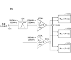
- FIG. 2 is a block diagram showing the configuration of a triple tuner for receiving divided bands
- FIG. 3 is a block diagram showing the configuration of a triple tuner for reception without band division.
- FIG. 4 is a connection diagram of a conventional distribution circuit.
- FIG. 5 is a graph showing simulation results for the distribution circuit of FIG.
- FIG. 6 is a connection diagram of a conventional distribution circuit.
- FIG. 7 is a graph showing simulation results of the distribution circuit of FIG.
- FIG. 8 is a connection diagram of a distribution circuit in which the element values of the configuration of FIG. 6 are changed.
- FIG. 9 is a graph showing simulation results of the distribution circuit of FIG.
- FIG. 10 is a connection diagram of a configuration in which conventional distribution circuits are cascaded.
- FIG. 11 is a graph showing simulation results of the distribution circuit of FIG.
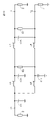
- FIG. 12 is a connection diagram of the first embodiment of the present technology.
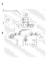
- FIG. 13 is a graph showing simulation results of the distribution circuit of FIG. 14 is a plan view of a substrate on which the distribution circuit of FIG. 12 is mounted on one side.
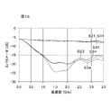
- FIG. 15 is a graph showing simulation results for the distribution circuit of FIG.
- FIG. 18 is a graph showing simulation results for the distribution circuit of FIG. 19 is a graph showing measurement results of the distribution circuit of FIG. 16.
- FIG. FIG. 20 is a plan view of one side of a substrate on which the distribution circuits of FIG. 16 are mounted on both sides.
- FIG. 21 is a plan view of the other side of the board on which the distribution circuits of FIG. 16 are mounted on both sides.
- FIG. 22 is a connection diagram of a 4-way distribution circuit to which the present technology is applied.
- FIG. 23 is a connection diagram of a two-way distribution circuit to which the present technology is applied.
- FIG. 24 is a connection diagram for explaining the construction of a 2-way distribution circuit using the configuration of the 3-way distribution circuit.
- a conventional distribution circuit will be described to facilitate understanding of one embodiment.
- tuner ICs compatible with 4K8K satellite broadcasting are beginning to spread.
- a signal from an antenna is input to a tuner IC 102 via an input terminal 101 such as an F connector or an IEC (International Electrotechnical Commission) connector.
- an input terminal 101 such as an F connector or an IEC (International Electrotechnical Commission) connector.
- IEC International Electrotechnical Commission
- a general configuration is that the signal is amplified once by the LNA 103 and then distributed to the tuner ICs 102a, 102b, and 102c using the distribution circuit 104.
- the overall configuration may be a tuner module using a mechanical shield or substrate, or may be an on-board using a substrate.
- the tuner ICs 102, 102a, 102b, and 102c have the same configuration, include mixers for selecting specific channels, variable gain amplifiers, filters, etc., and output IF signals.
- An IF signal is provided to a demodulation module (not shown).
- a tuner having a configuration called an IQ detector or a Zero-IF tuner may be used as the tuner ICs 102, 102a, 102b, 102c. In this case, an I-axis output and a Q-axis output are output.
- the band (2224 MHz-3224 MHz) is divided into two bands by the splitter 105, the signals of each band are supplied to the distribution circuits 104H and 104L via the LNA 103H and LNA 103L, and the tuner ICs 102a, 102b, 102c was designed to input signals to two terminals for each band.
- the LNA 113 and tuner ICs 112a, 112b, and 112c that can handle these bands in one band have been developed, so the branching filter is no longer necessary and one distribution circuit 114 is provided as shown in FIG.
- the signal input terminal of IC also becomes one terminal.
- the distribution circuit 114 a wideband distribution circuit of (1032 MHz-3224 MHz) corresponding to one system is required.
- the present technology provides a distribution circuit that can be applied to this broadband distribution circuit 114 .
- the Wilkinson distribution circuit with the configuration of the lumped constant circuit described in Patent Document 1 has the configuration shown in FIG. A simulation result of this distribution circuit is shown in FIG.
- An input terminal T1 (first signal terminal) is provided with an impedance Z (for example, 50 ⁇ or 75 ⁇ ) as a terminating resistor.
- An input capacitor C1 is connected between the input terminal T1 and ground.
- a low-pass filter consisting of a coil L9 and a capacitor C11 is inserted between the input terminal T1 and the output terminal T2 (second terminal).
- a low-pass filter composed of a coil L8 and a capacitor C10 is inserted between the input terminal T1 and the output terminal T3 (third terminal).
- a low-pass filter composed of a coil L3 and a capacitor C9 is inserted between the input terminal T1 and the output terminal T4 (fourth terminal).
- the output terminals T2, T3, T4 are each terminated with an impedance Z (eg, 50 ⁇ ).
- the output terminals T2, T3 and T4 are commonly connected via resistors R10, R9 and R6.
- the simulation was performed in steps of 0.01 GHz in the frequency range from 0.01 GHz to 3.5 GHz. Simulation results are expressed using S-parameters.
- S-parameters S21, S31, and S41 representing pass characteristics from the input terminal T1 to the output terminals T2, T3, and T4, and S-parameters S23, S24, and S34 representing isolation characteristics between the output terminals are distributed. It is important for evaluating circuit characteristics.
- the isolation characteristic should have a lower value, and the pass characteristic should have a higher value. Poor isolation characteristics may cause interference with other tuner ICs when the tuner ICs simultaneously receive signals in a multi-tuner IC, resulting in reception failure. In addition, poor pass characteristics cause sensitivity degradation.
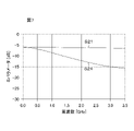
- FIG. 5 shows S-parameter S21 (transmission characteristic from input terminal T1 to output terminal T2) and S-parameter 24 (isolation characteristic between output terminals T2 and T4).
- S-parameters S31 and S41 are the same as the S-parameters S21
- the S-parameters S23 and S34 are: It is the same as the S parameter S24.
- the simulation results described below when only the S-parameter 21 and the S-parameter S24 are shown, it means that the other S-parameters are similar. From the simulation results of FIG. 5, it can be seen that the pass characteristics are good, but the isolation characteristics in the low frequency range are insufficient. For example, an isolation characteristic (target value) of 15 dB at 1 GHz has not been achieved.
- FIG. 6 shows a circuit configuration in which the connection of resistors R6, R9, and R10 in the circuit configuration of FIG. 4 is modified using star-delta conversion. Simulation results for the circuit of FIG. 6 are shown in FIG. The value of each element is the same as the value of the element in FIG. This simulation result is almost the same as the simulation result of FIG. 5, indicating that the isolation characteristics in the low frequency range are insufficient.
- FIG. 8 shows the configuration of a distribution circuit that employs such a method. Although the connection is the same as that of the distribution circuit of FIG. 6, each element has the following values.
- a low-pass filter comprising a coil L9 and a capacitor C11 and a low-pass filter comprising a coil L6 and a capacitor C16 are cascaded between the input terminal T1 and the output terminal T2 (second terminal).
- a low-pass filter comprising a coil L8 and a capacitor C10 and a low-pass filter comprising a coil L7 and a capacitor C15 are cascaded between the input terminal T1 and the output terminal T3 (third terminal).
- a low-pass filter comprising a coil L3 and a capacitor C9 and a low-pass filter comprising a coil L5 and a capacitor C14 are cascaded between the input terminal T1 and the output terminal T4 (fourth terminal).
- the output of the low-pass filter consisting of the coil L9 and the capacitor C11 and the output of the low-pass filter consisting of the coil L8 and the capacitor C10 are connected via the resistor R9.
- the output of the low-pass filter consisting of coil L9 and capacitor C11 and the output of the low-pass filter consisting of coil L3 and capacitor C9 are connected via resistor R10.
- the output of the low-pass filter consisting of coil L8 and capacitor C10 and the output of the low-pass filter consisting of coil L3 and capacitor C9 are connected via resistor R6.
- resistor R7 and a resistor R8 are inserted between the output terminal T2 and the output terminals T3 and T4, respectively, and a resistor R12 is inserted between the output terminal T3 and the output terminal T4.
- resistors R8, R7 and R12 function as matching resistors, thereby improving isolation characteristics.
- each element is not completely the same between the first-stage Wilkinson-type distribution circuit and the second-stage Wilkinson-type distribution circuit, but is an adjusted value.
- FIG. 11 shows simulation results for the distribution circuit having the configuration of FIG. Although the isolation characteristics have been considerably improved, the target value (15 dB at 1 GHz) for isolation characteristics on the low frequency side has not been achieved.
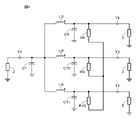
- FIG. 12 shows the configuration of an embodiment in which the present technology is applied to a distribution circuit that distributes an input signal into three.
- Input terminal (first terminal) T1, output terminal (second terminal) T2, output terminal (third terminal) T3, and output terminal T4 (fourth terminal) have impedance Z (for example, 50 ⁇ ) as a terminating resistor. It is connected.
- An input capacitor C1 is connected between the input terminal T1 and ground.
- An input signal from the input terminal T1 is divided into three signal systems respectively corresponding to the output terminals T2, T3 and T4.
- a low-pass filter consisting of a coil L9 and a capacitor C11 and a coil L6 are cascaded between the input terminal T1 and the output terminal T2.
- a low-pass filter composed of a coil L8 and a capacitor C10 and a coil L7 are cascaded between the input terminal T1 and the output terminal T3.
- a low-pass filter composed of a coil L3 and a capacitor C9 and a coil L5 are cascade-connected between the input terminal T1 and the output terminal T4.
- a capacitor C15 and a resistor R7 are connected in parallel between the connection point of the coil L6 and the output terminal T2 and the connection point of the coil L7 and the output terminal T3.
- a capacitor C14 and a resistor R12 are connected in parallel between the connection point of the coil L7 and the output terminal T3 and the connection point of the coil L5 and the output terminal T4.
- a capacitor C16 and a resistor R8 are connected in parallel between the connection point of the coil L5 and the output terminal T4 and the connection point of the coil L6 and the output terminal T2.
- Coils L9, L8, L3, capacitors C11, C10, C9, and resistors R10, R9, R6 constitute a first-stage Wilkinson distribution circuit.
- Coils L6, L7, L5, capacitors C16, C15, C14, and resistors R8, R7, R12 form a second-stage Wilkinson distribution circuit.
- the circuit configuration shown in FIG. 12 is parallel to isolation resistors R7, R12, and R8 inserted between output terminals T2 and T3, between output terminals T3 and T4, and between output terminals T4 and T2, respectively.
- a capacitor C15, a capacitor C14, and a capacitor C16 are connected to .
- These capacitors (0.2 [pF]) and the coils L6, L7, and L5 (3.9 [nH]) connected in front of them form isolation poles.
- side isolation characteristics can be improved. Also, by shifting the values of the elements in the first and second stages, the isolation characteristics can be improved.
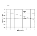
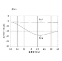
- FIG. 13 shows simulation results for the distribution circuit with the configuration in FIG. According to the simulation results, the target value (15 dB at 1 GHz) for isolation characteristics on the low-frequency side was slightly not achieved, but as will be described later, the target was achieved with actual measurements.
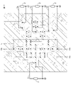
- FIG. 12 An example of a board on which the circuit shown in FIG. 12 is mounted is shown in FIG.
- the elements are mounted on one surface of the substrate (referred to as surface A as appropriate) except for the signal line that connects one end of the resistor R10 to the connection point of the coils L3 and L5.
- surface A the substrate
- Single-sided mounting can reduce manufacturing costs compared to double-sided mounting.
- the signal line connecting one end of the resistor R10 to the connection point of the coil L3 and the coil L5 crosses other signal lines, making it difficult to wire on the A side of the substrate. 14, wiring is carried out on the other surface (referred to as B surface as appropriate). Since this wiring is relatively long, it cannot be ignored for high frequency signals.
- the wiring becomes a stub for the signal line connecting the resistors R10, R9, and R6.
- the wiring portion L between R10 and R6 in FIG. 12 corresponds to the stub.
- the places with ⁇ in the center of the hatched circles are through holes for signal wiring, and the places without ⁇ in the center of the hatched circles are through holes that are connected to GND on other layers of the board. indicate the hole.
- a wiring portion L is formed between the through holes Ha and Hb.
- Hc is a through hole connected to GND.
- the layer structure of the substrate may be a double-sided board, a four-layer board, or other layer structure.
- Fig. 15 shows the simulation results of the board (Fig. 14) on which stubs are generated.
- the simulation results show that the pass characteristics on the higher frequency side than 2 GHz are significantly degraded (especially the pass characteristics of the output terminal T4).
- characteristic S41 This is because there is no resistance on the output terminal T4 side, and if a stub is formed on the B side of the substrate, a phase-shifted signal that has passed through that path returns to the output terminal T4 and cancels out the desired signal.
- the pass characteristics are significantly degraded on the high frequency side.
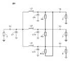
- connection point of coil L9 and coil L6 (the output of the low-pass filter consisting of coil L9 and capacitor C11) is connected to coil L3 and coil L5 through resistor R10 and resistor R13. (output of low-pass filter consisting of coil L3 and capacitor C9).
- An example of substrate mounting in this case is shown in FIG.
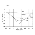
- resistor R13 By adding resistor R13, the effect of the stub can be suppressed, as can be seen from the simulation results shown in FIG. That is, it is possible to prevent the pass characteristic S41 related to the output terminal T4 from attenuating on the high frequency side.
- FIG. 19 shows characteristics evaluated (measured) by actually making a prototype substrate. It was possible to obtain characteristics that generally agreed with the simulation results, and the target isolation characteristic of 15 dB was achieved.
- both sides (A side and B side) of the substrate may be used to mount the distribution circuit.
- 20 and 21 show examples in which the circuit having the configuration shown in FIG. 16 is mounted on both sides of the substrate.
- FIG. 20 shows the A-side pattern
- FIG. 21 shows the B-side pattern.
- the patterns on the A side and the B side are connected via through holes.
- the isolation resistors R10, R9, R6, and R13 are inserted between the output terminals, they should be placed near the respective signal lines (wiring patterns) to prevent deterioration of the transmission characteristics. can be done.
- the layer structure of the substrate may be a double-sided board, a four-layer board, or other layer structure.
- FIG. 22 shows a configuration for distributing an input signal to four output terminals T2, T3, T4 and T5.
- a first-stage Wilkinson distribution circuit (coil L10, capacitor C18, resistor R14) is added to the configuration of FIG. A distribution circuit has been added.
- Fig. 23 shows a configuration example of a two-way distribution circuit.
- a circuit is provided for input terminal T1 and output terminals T2 and T3. Furthermore, as shown in FIG. 24, the configuration of the three-way distribution circuit is laid out on the substrate.
- NM No mount
- a two-way distribution circuit can be realized by not mounting the element.
- the present technology can realize a distribution circuit that has both pass characteristics and isolation characteristics in a wide band (1032 MHz to 3224 MHz).
- the circuit of the present technology can be mounted on a single-sided substrate.
- the present technology can configure a distribution circuit with a desired number of distributions, such as two-way distribution, three-way distribution, and four-way distribution, and has excellent versatility.
- the present technology is not limited to the above-described embodiments, and various modifications based on the technical idea of the present technology are possible.
- the present technology is not limited to the band (1032 MHz to 3224 MHz), and can be applied to other bands by changing the element values.
- the present technology can be used not only in broadcasting but also in the field of communication.
- the synthesis circuit may be configured by switching the input and the output such that the input terminal is used as the output terminal and the output terminal is used as the input terminal.
- the present technology can also adopt the following configurations.
- (1) A signal in which a second terminal and a third terminal are connected to the first terminal via two coils, respectively, and a resistor and a capacitor are connected in parallel between the second terminal and the third terminal processing circuit.
- (2) The signal processing circuit according to (1), wherein a signal is input to the first terminal and signals are output from the second terminal and the third terminal.
- (3) The signal processing circuit according to (1), wherein a signal is input to the second terminal and the third terminal, and a signal is output from the first terminal.
- a Wilkinson type distribution circuit composed of a coil, a capacitor, and a resistor is cascade-connected in two stages between the first terminal, the second terminal, and the third terminal, A signal processing circuit in which a capacitor is connected in parallel with a resistor inserted between the second terminal and the third terminal in one of the Wilkinson distribution circuits.
- T1 input terminal
- T2, T3, T4 output terminal
- C1 input capacitor
Landscapes
- Engineering & Computer Science (AREA)
- Microelectronics & Electronic Packaging (AREA)
- Physics & Mathematics (AREA)
- Electromagnetism (AREA)
- Networks Using Active Elements (AREA)
- Amplifiers (AREA)
- Input Circuits Of Receivers And Coupling Of Receivers And Audio Equipment (AREA)
- Filters And Equalizers (AREA)
Abstract
Description
また、本技術は、第1の端子と第2の端子及び第3の端子の間に、コイル、コンデンサ及び抵抗により構成されたウィルキンソン型分配回路が2段縦続接続され、
一方のウィルキンソン型分配回路において第2の端子及び第3の端子間に挿入された抵抗と並列にコンデンサが接続された信号処理回路である。
さらに、本技術は、入力端子と少なくとも3個の出力端子の間に、コイル、コンデンサ及び抵抗により構成されたウィルキンソン型分配回路が2段縦続接続され、
後段のウィルキンソン型分配回路において出力端子間に挿入された抵抗と並列にコンデンサが接続された分配回路である。
C9,C10,C11=0.2[pF]、R6,R9,R10=220[Ω]
C9,C10,C11=0.2[pF]、R6,R9,R10=220[Ω]
Z=50[Ω]、C1=0.2[pF]、L3,L8,L9=4.7[nH]、
C9,C10,C11=0.2[pF]、R6,R9,R10=220[Ω]
L5,L7,L6=3.9[nH]、
C14,C15,C16=0.2[pF]、R12,R7,R8=330[Ω]
Z=50[Ω]、C1=0.2[pF]、L3,L8,L9=4.7[nH]、
C9,C10,C11=0.2[pF]、R6,R9,R10=220[Ω]
L5,L7,L6=3.9[nH]、
C14,C15,C16=0.2[pF]、R12,R7,R8=330[Ω]
Z=50[Ω]、C1=0.2[pF]、L3,L8,L9=4.7[nH]、
C9,C10,C11=0.2[pF]、R6,R9,=220[Ω]
R10、R13=560[Ω]
L5,L7,L6=3.9[nH]、
C14,C15,C16=0.2[pF]、R12,R7,R8=330[Ω]
Z=50[Ω]、C1=0.2[pF]、L3,L8,L9,L10=4.7[nH]、C9,C10,C11,C18=0.2[pF]、R9,R6,R14=220[Ω]
R10、R13=560[Ω]
L5,L7,L6,L11=3.9[nH]、
C17,C14,C15,C16,=0.2[pF]、R15,R12,R7,R8=330 [Ω]
Z=50[Ω]、C1=0.2[pF]、L8,L9=4.7[nH]、
C10,C11=0.2[pF]、R9=220[Ω]
L7,L6=3.9[nH]、
C15=0.2[pF]、R7=330[Ω]
(1)
第1の端子に対して2つのコイルをそれぞれ介して第2の端子及び第3の端子が接続され、前記第2の端子及び前記第3の端子間に抵抗及びコンデンサが並列に接続された信号処理回路。
(2)
前記第1の端子に信号が入力され、前記第2の端子及び前記第3の端子から信号が出力される(1)に記載の信号処理回路。
(3)
前記第2の端子及び前記第3の端子に信号が入力され、前記前記第1の端子から信号が出力される(1)に記載の信号処理回路。
(4)
第1の端子と第2の端子及び第3の端子の間に、コイル、コンデンサ及び抵抗により構成されたウィルキンソン型分配回路が2段縦続接続され、
一方の前記ウィルキンソン型分配回路において前記第2の端子及び前記第3の端子間に挿入された抵抗と並列にコンデンサが接続された信号処理回路。
(5)
前記第1の端子に信号が入力され、前記第2の端子及び前記第3の端子から信号が出力される(4)に記載の信号処理回路。
(6)
前記第2の端子及び前記第3の端子に信号が入力され、前記第1の端子から信号が出力される(4)に記載の信号処理回路。
(7)
入力端子と少なくとも3個の出力端子の間に、コイル、コンデンサ及び抵抗により構成されたウィルキンソン型分配回路が2段縦続接続され、
後段の前記ウィルキンソン型分配回路において前記出力端子間に挿入された抵抗と並列にコンデンサが接続された分配回路。
(8)
前段の前記ウィルキンソン型分配回路において複数の前記出力端子に対応する信号系統間に挿入された複数の抵抗中の一つの抵抗と直列に抵抗を接続した(7)に記載の分配回路。
(9)
基板片面に実装されたパターンにおいて離れた位置の信号系統間に挿入される抵抗に対して前記抵抗が直列に接続されるようにした(8)に記載の分配回路。
(10)
(7)7の分配回路を実装可能なようにパターンが形成された基板上で、1又は複数の信号系統に含まれる素子を実装しないことによってより少ない出力を得るようにした分配回路。
101・・・アンテナからの信号の入力端子、102,102a,102b,102c・・・チューナーIC、104,114・・・分配回路
Claims (10)
- 第1の端子に対して2つのコイルをそれぞれ介して第2の端子及び第3の端子が接続され、前記第2の端子及び前記第3の端子間に抵抗及びコンデンサが並列に接続された信号処理回路。
- 前記第1の端子に信号が入力され、前記第2の端子及び前記第3の端子から信号が出力される請求項1に記載の信号処理回路。
- 前記第2の端子及び前記第3の端子に信号が入力され、前記前記第1の端子から信号が出力される請求項1に記載の信号処理回路。
- 第1の端子と第2の端子及び第3の端子の間に、コイル、コンデンサ及び抵抗により構成されたウィルキンソン型分配回路が2段縦続接続され、
一方の前記ウィルキンソン型分配回路において前記第2の端子及び前記第3の端子間に挿入された抵抗と並列にコンデンサが接続された信号処理回路。 - 前記第1の端子に信号が入力され、前記第2の端子及び前記第3の端子から信号が出力される請求項4に記載の信号処理回路。
- 前記第2の端子及び前記第3の端子に信号が入力され、前記第1の端子から信号が出力される請求項4に記載の信号処理回路。
- 入力端子と少なくとも3個の出力端子の間に、コイル、コンデンサ及び抵抗により構成されたウィルキンソン型分配回路が2段縦続接続され、
後段の前記ウィルキンソン型分配回路において前記出力端子間に挿入された抵抗と並列にコンデンサが接続された分配回路。 - 前段の前記ウィルキンソン型分配回路において複数の前記出力端子に対応する信号系統間に挿入された複数の抵抗中の一つの抵抗と直列に抵抗を接続した請求項7に記載の分配回路。
- 基板片面に実装されたパターンにおいて離れた位置の信号系統間に挿入される抵抗に対して前記抵抗が直列に接続されるようにした請求項8に記載の分配回路。
- 請求項7の分配回路を実装可能なようにパターンが形成された基板上で、1又は複数の信号系統に含まれる素子を実装しないことによってより少ない出力を得るようにした分配回路。
Priority Applications (2)
| Application Number | Priority Date | Filing Date | Title |
|---|---|---|---|
| US18/261,442 US20240072406A1 (en) | 2021-01-21 | 2021-12-09 | Signal processing circuit and distribution circuit |
| JP2022577023A JP7781082B2 (ja) | 2021-01-21 | 2021-12-09 | 分配回路 |
Applications Claiming Priority (2)
| Application Number | Priority Date | Filing Date | Title |
|---|---|---|---|
| JP2021-008267 | 2021-01-21 | ||
| JP2021008267 | 2021-01-21 |
Publications (1)
| Publication Number | Publication Date |
|---|---|
| WO2022158156A1 true WO2022158156A1 (ja) | 2022-07-28 |
Family
ID=82548325
Family Applications (1)
| Application Number | Title | Priority Date | Filing Date |
|---|---|---|---|
| PCT/JP2021/045252 Ceased WO2022158156A1 (ja) | 2021-01-21 | 2021-12-09 | 信号処理回路および分配回路 |
Country Status (3)
| Country | Link |
|---|---|
| US (1) | US20240072406A1 (ja) |
| JP (1) | JP7781082B2 (ja) |
| WO (1) | WO2022158156A1 (ja) |
Cited By (1)
| Publication number | Priority date | Publication date | Assignee | Title |
|---|---|---|---|---|
| WO2025070404A1 (ja) * | 2023-09-26 | 2025-04-03 | 株式会社ヨコオ | 電子部品、アンテナ装置 |
Citations (3)
| Publication number | Priority date | Publication date | Assignee | Title |
|---|---|---|---|---|
| JPH02170625A (ja) * | 1988-12-22 | 1990-07-02 | Toshiba Corp | 高周波電力分配器 |
| JP2010534438A (ja) * | 2007-07-24 | 2010-11-04 | トムソン ライセンシング | 多アンテナシステム給電デバイスおよびかかるデバイスを備える無線リンク端末 |
| WO2020121985A1 (ja) * | 2018-12-12 | 2020-06-18 | 株式会社村田製作所 | 電力分配器 |
Family Cites Families (7)
| Publication number | Priority date | Publication date | Assignee | Title |
|---|---|---|---|---|
| KR19980014205A (ko) * | 1996-08-08 | 1998-05-25 | 김광호 | 고주파 전력분배기/결합기 회로 |
| DE102015212232B4 (de) * | 2015-06-30 | 2020-03-05 | TRUMPF Hüttinger GmbH + Co. KG | Leistungscombiner zur Kopplung von Hochfrequenzsignalen und Leistungscombineranordnung mit einem solchen Leistungscombiner |
| US9667216B2 (en) * | 2015-08-12 | 2017-05-30 | Shure Acquisition Holdings, Inc. | Wideband tunable combiner system |
| US10608313B2 (en) * | 2018-01-08 | 2020-03-31 | Linear Technology Holding Llc | Wilkinson combiner with coupled inductors |
| CN214851156U (zh) * | 2018-08-30 | 2021-11-23 | 株式会社村田制作所 | 功率分配/耦合电路和功率分配/耦合部件 |
| KR102703276B1 (ko) * | 2019-01-09 | 2024-09-05 | 삼성전자 주식회사 | 위상 어레이 시스템을 위한 4방향 전력 분배기 및 결합기 |
| US11043931B2 (en) * | 2019-11-04 | 2021-06-22 | Analog Devices International Unlimited Company | Power combiner/divider |
-
2021
- 2021-12-09 JP JP2022577023A patent/JP7781082B2/ja active Active
- 2021-12-09 US US18/261,442 patent/US20240072406A1/en active Pending
- 2021-12-09 WO PCT/JP2021/045252 patent/WO2022158156A1/ja not_active Ceased
Patent Citations (3)
| Publication number | Priority date | Publication date | Assignee | Title |
|---|---|---|---|---|
| JPH02170625A (ja) * | 1988-12-22 | 1990-07-02 | Toshiba Corp | 高周波電力分配器 |
| JP2010534438A (ja) * | 2007-07-24 | 2010-11-04 | トムソン ライセンシング | 多アンテナシステム給電デバイスおよびかかるデバイスを備える無線リンク端末 |
| WO2020121985A1 (ja) * | 2018-12-12 | 2020-06-18 | 株式会社村田製作所 | 電力分配器 |
Cited By (1)
| Publication number | Priority date | Publication date | Assignee | Title |
|---|---|---|---|---|
| WO2025070404A1 (ja) * | 2023-09-26 | 2025-04-03 | 株式会社ヨコオ | 電子部品、アンテナ装置 |
Also Published As
| Publication number | Publication date |
|---|---|
| JPWO2022158156A1 (ja) | 2022-07-28 |
| US20240072406A1 (en) | 2024-02-29 |
| JP7781082B2 (ja) | 2025-12-05 |
Similar Documents
| Publication | Publication Date | Title |
|---|---|---|
| CN108809336B (zh) | 用于射频滤波器的系统和方法 | |
| US10854945B2 (en) | Circuits for wireless communication on multiple frequency bands | |
| US20100007433A1 (en) | Power Splitter/Combiner | |
| US20100244981A1 (en) | Radio frequency power divider and combiner circuit | |
| US8395460B2 (en) | Low loss RF transceiver combiner | |
| CN1173054A (zh) | 平衡-不平衡变换器 | |
| US6970688B2 (en) | Local oscillator signal divider and low-noise converter employing the same | |
| US20100097160A1 (en) | Directional coupler | |
| KR20080008249A (ko) | 결합된 섹션을 갖는 분할기/조합기 | |
| WO2012117072A2 (de) | Verstärkermodul | |
| JP7781082B2 (ja) | 分配回路 | |
| US5285175A (en) | Tri-phase combiner/splitter system | |
| CN101651485A (zh) | 降低交互调变干扰的方法及其所应用的信号接收器 | |
| CN115732879B (zh) | 一种具有无反射特性的平衡-不平衡一分三滤波功分器 | |
| CN118738804A (zh) | 一种宽带全端口无反射滤波功分器 | |
| CN217607788U (zh) | 一种射频微波开关矩阵电路及器件 | |
| Yang et al. | Transitioning to RF filtering | |
| US5128638A (en) | Four-post quadrature coupler suitable for monolithic implementation | |
| CN105186076A (zh) | 一种基于ltcc的s波段自负载四路正交滤波器 | |
| CN216390945U (zh) | 一种移相网络 | |
| CN110011680B (zh) | 一种射频通信模组及其模拟消噪电路 | |
| US12519447B2 (en) | Electronic component and communication apparatus | |
| CN120238067B (zh) | 基于电桥的频分双工平衡式低噪声放大器及射频接收机 | |
| Zhu et al. | Balanced microstrip circuit with differential negative group delay characteristics | |
| EP3701629B1 (en) | Radio frequency front end for wireless communication |
Legal Events
| Date | Code | Title | Description |
|---|---|---|---|
| 121 | Ep: the epo has been informed by wipo that ep was designated in this application |
Ref document number: 21921258 Country of ref document: EP Kind code of ref document: A1 |
|
| ENP | Entry into the national phase |
Ref document number: 2022577023 Country of ref document: JP Kind code of ref document: A |
|
| WWE | Wipo information: entry into national phase |
Ref document number: 18261442 Country of ref document: US |
|
| NENP | Non-entry into the national phase |
Ref country code: DE |
|
| 122 | Ep: pct application non-entry in european phase |
Ref document number: 21921258 Country of ref document: EP Kind code of ref document: A1 |