WO2022149576A1 - Photoelectric conversion device and photodetection system - Google Patents
Photoelectric conversion device and photodetection system Download PDFInfo
- Publication number
- WO2022149576A1 WO2022149576A1 PCT/JP2022/000096 JP2022000096W WO2022149576A1 WO 2022149576 A1 WO2022149576 A1 WO 2022149576A1 JP 2022000096 W JP2022000096 W JP 2022000096W WO 2022149576 A1 WO2022149576 A1 WO 2022149576A1
- Authority
- WO
- WIPO (PCT)
- Prior art keywords
- photoelectric conversion
- conversion device
- exposure period
- signal
- switch
- Prior art date
Links
- 238000006243 chemical reaction Methods 0.000 title claims abstract description 174
- 230000007274 generation of a signal involved in cell-cell signaling Effects 0.000 claims abstract description 13
- 238000012545 processing Methods 0.000 claims description 59
- 238000012937 correction Methods 0.000 claims description 27
- 238000007493 shaping process Methods 0.000 claims description 22
- 238000000034 method Methods 0.000 claims description 21
- 230000006870 function Effects 0.000 claims description 13
- 238000010791 quenching Methods 0.000 claims description 13
- 230000008569 process Effects 0.000 claims description 11
- 230000000171 quenching effect Effects 0.000 claims description 4
- 238000005259 measurement Methods 0.000 claims description 3
- 238000001514 detection method Methods 0.000 description 43
- 230000003287 optical effect Effects 0.000 description 27
- 238000010586 diagram Methods 0.000 description 23
- 239000004065 semiconductor Substances 0.000 description 14
- 239000010410 layer Substances 0.000 description 12
- 210000005252 bulbus oculi Anatomy 0.000 description 10
- 230000008859 change Effects 0.000 description 10
- 239000000758 substrate Substances 0.000 description 10
- 238000003384 imaging method Methods 0.000 description 9
- 230000000694 effects Effects 0.000 description 8
- ORQBXQOJMQIAOY-UHFFFAOYSA-N nobelium Chemical compound [No] ORQBXQOJMQIAOY-UHFFFAOYSA-N 0.000 description 8
- 230000005856 abnormality Effects 0.000 description 7
- 230000000052 comparative effect Effects 0.000 description 7
- 238000002674 endoscopic surgery Methods 0.000 description 7
- 238000007781 pre-processing Methods 0.000 description 6
- 210000001519 tissue Anatomy 0.000 description 6
- 238000004891 communication Methods 0.000 description 5
- 210000003128 head Anatomy 0.000 description 5
- 230000005284 excitation Effects 0.000 description 4
- 239000004984 smart glass Substances 0.000 description 4
- 230000000007 visual effect Effects 0.000 description 4
- 230000015556 catabolic process Effects 0.000 description 3
- 230000007423 decrease Effects 0.000 description 3
- 230000001678 irradiating effect Effects 0.000 description 3
- 210000004204 blood vessel Anatomy 0.000 description 2
- 239000003153 chemical reaction reagent Substances 0.000 description 2
- 230000007547 defect Effects 0.000 description 2
- 238000011161 development Methods 0.000 description 2
- MOFVSTNWEDAEEK-UHFFFAOYSA-M indocyanine green Chemical compound [Na+].[O-]S(=O)(=O)CCCCN1C2=CC=C3C=CC=CC3=C2C(C)(C)C1=CC=CC=CC=CC1=[N+](CCCCS([O-])(=O)=O)C2=CC=C(C=CC=C3)C3=C2C1(C)C MOFVSTNWEDAEEK-UHFFFAOYSA-M 0.000 description 2
- 229960004657 indocyanine green Drugs 0.000 description 2
- 230000001179 pupillary effect Effects 0.000 description 2
- 230000011514 reflex Effects 0.000 description 2
- 230000007704 transition Effects 0.000 description 2
- 238000012935 Averaging Methods 0.000 description 1
- 230000004913 activation Effects 0.000 description 1
- 230000004888 barrier function Effects 0.000 description 1
- 239000000969 carrier Substances 0.000 description 1
- 238000007906 compression Methods 0.000 description 1
- 230000006835 compression Effects 0.000 description 1
- 210000004087 cornea Anatomy 0.000 description 1
- 230000006866 deterioration Effects 0.000 description 1
- 238000010336 energy treatment Methods 0.000 description 1
- 238000002073 fluorescence micrograph Methods 0.000 description 1
- 239000011521 glass Substances 0.000 description 1
- 238000010030 laminating Methods 0.000 description 1
- 230000031700 light absorption Effects 0.000 description 1
- 238000002156 mixing Methods 0.000 description 1
- 238000012986 modification Methods 0.000 description 1
- 230000004048 modification Effects 0.000 description 1
- 210000004400 mucous membrane Anatomy 0.000 description 1
- 230000000737 periodic effect Effects 0.000 description 1
- 238000002360 preparation method Methods 0.000 description 1
- 230000002265 prevention Effects 0.000 description 1
- 210000001747 pupil Anatomy 0.000 description 1
- 238000007789 sealing Methods 0.000 description 1
- 239000002344 surface layer Substances 0.000 description 1
- 238000001356 surgical procedure Methods 0.000 description 1
- 230000001360 synchronised effect Effects 0.000 description 1
- 230000002194 synthesizing effect Effects 0.000 description 1
Images


Classifications
-
- H—ELECTRICITY
- H04—ELECTRIC COMMUNICATION TECHNIQUE
- H04N—PICTORIAL COMMUNICATION, e.g. TELEVISION
- H04N25/00—Circuitry of solid-state image sensors [SSIS]; Control thereof
- H04N25/70—SSIS architectures; Circuits associated therewith
- H04N25/76—Addressed sensors, e.g. MOS or CMOS sensors
- H04N25/77—Pixel circuitry, e.g. memories, A/D converters, pixel amplifiers, shared circuits or shared components
-
- H—ELECTRICITY
- H01—ELECTRIC ELEMENTS
- H01L—SEMICONDUCTOR DEVICES NOT COVERED BY CLASS H10
- H01L31/00—Semiconductor devices sensitive to infrared radiation, light, electromagnetic radiation of shorter wavelength or corpuscular radiation and specially adapted either for the conversion of the energy of such radiation into electrical energy or for the control of electrical energy by such radiation; Processes or apparatus specially adapted for the manufacture or treatment thereof or of parts thereof; Details thereof
- H01L31/02—Details
- H01L31/02016—Circuit arrangements of general character for the devices
- H01L31/02019—Circuit arrangements of general character for the devices for devices characterised by at least one potential jump barrier or surface barrier
- H01L31/02027—Circuit arrangements of general character for the devices for devices characterised by at least one potential jump barrier or surface barrier for devices working in avalanche mode
-
- G—PHYSICS
- G01—MEASURING; TESTING
- G01J—MEASUREMENT OF INTENSITY, VELOCITY, SPECTRAL CONTENT, POLARISATION, PHASE OR PULSE CHARACTERISTICS OF INFRARED, VISIBLE OR ULTRAVIOLET LIGHT; COLORIMETRY; RADIATION PYROMETRY
- G01J1/00—Photometry, e.g. photographic exposure meter
- G01J1/42—Photometry, e.g. photographic exposure meter using electric radiation detectors
- G01J1/44—Electric circuits
-
- H—ELECTRICITY
- H01—ELECTRIC ELEMENTS
- H01L—SEMICONDUCTOR DEVICES NOT COVERED BY CLASS H10
- H01L31/00—Semiconductor devices sensitive to infrared radiation, light, electromagnetic radiation of shorter wavelength or corpuscular radiation and specially adapted either for the conversion of the energy of such radiation into electrical energy or for the control of electrical energy by such radiation; Processes or apparatus specially adapted for the manufacture or treatment thereof or of parts thereof; Details thereof
- H01L31/08—Semiconductor devices sensitive to infrared radiation, light, electromagnetic radiation of shorter wavelength or corpuscular radiation and specially adapted either for the conversion of the energy of such radiation into electrical energy or for the control of electrical energy by such radiation; Processes or apparatus specially adapted for the manufacture or treatment thereof or of parts thereof; Details thereof in which radiation controls flow of current through the device, e.g. photoresistors
- H01L31/10—Semiconductor devices sensitive to infrared radiation, light, electromagnetic radiation of shorter wavelength or corpuscular radiation and specially adapted either for the conversion of the energy of such radiation into electrical energy or for the control of electrical energy by such radiation; Processes or apparatus specially adapted for the manufacture or treatment thereof or of parts thereof; Details thereof in which radiation controls flow of current through the device, e.g. photoresistors characterised by potential barriers, e.g. phototransistors
- H01L31/101—Devices sensitive to infrared, visible or ultraviolet radiation
- H01L31/102—Devices sensitive to infrared, visible or ultraviolet radiation characterised by only one potential barrier
- H01L31/107—Devices sensitive to infrared, visible or ultraviolet radiation characterised by only one potential barrier the potential barrier working in avalanche mode, e.g. avalanche photodiodes
-
- H—ELECTRICITY
- H04—ELECTRIC COMMUNICATION TECHNIQUE
- H04N—PICTORIAL COMMUNICATION, e.g. TELEVISION
- H04N25/00—Circuitry of solid-state image sensors [SSIS]; Control thereof
- H04N25/40—Extracting pixel data from image sensors by controlling scanning circuits, e.g. by modifying the number of pixels sampled or to be sampled
-
- H—ELECTRICITY
- H04—ELECTRIC COMMUNICATION TECHNIQUE
- H04N—PICTORIAL COMMUNICATION, e.g. TELEVISION
- H04N25/00—Circuitry of solid-state image sensors [SSIS]; Control thereof
- H04N25/50—Control of the SSIS exposure
- H04N25/57—Control of the dynamic range
- H04N25/58—Control of the dynamic range involving two or more exposures
-
- H—ELECTRICITY
- H04—ELECTRIC COMMUNICATION TECHNIQUE
- H04N—PICTORIAL COMMUNICATION, e.g. TELEVISION
- H04N25/00—Circuitry of solid-state image sensors [SSIS]; Control thereof
- H04N25/70—SSIS architectures; Circuits associated therewith
- H04N25/76—Addressed sensors, e.g. MOS or CMOS sensors
- H04N25/77—Pixel circuitry, e.g. memories, A/D converters, pixel amplifiers, shared circuits or shared components
- H04N25/772—Pixel circuitry, e.g. memories, A/D converters, pixel amplifiers, shared circuits or shared components comprising A/D, V/T, V/F, I/T or I/F converters
- H04N25/773—Pixel circuitry, e.g. memories, A/D converters, pixel amplifiers, shared circuits or shared components comprising A/D, V/T, V/F, I/T or I/F converters comprising photon counting circuits, e.g. single photon detection [SPD] or single photon avalanche diodes [SPAD]
-
- H—ELECTRICITY
- H04—ELECTRIC COMMUNICATION TECHNIQUE
- H04N—PICTORIAL COMMUNICATION, e.g. TELEVISION
- H04N25/00—Circuitry of solid-state image sensors [SSIS]; Control thereof
- H04N25/70—SSIS architectures; Circuits associated therewith
- H04N25/79—Arrangements of circuitry being divided between different or multiple substrates, chips or circuit boards, e.g. stacked image sensors
-
- G—PHYSICS
- G01—MEASURING; TESTING
- G01J—MEASUREMENT OF INTENSITY, VELOCITY, SPECTRAL CONTENT, POLARISATION, PHASE OR PULSE CHARACTERISTICS OF INFRARED, VISIBLE OR ULTRAVIOLET LIGHT; COLORIMETRY; RADIATION PYROMETRY
- G01J1/00—Photometry, e.g. photographic exposure meter
- G01J1/42—Photometry, e.g. photographic exposure meter using electric radiation detectors
- G01J1/44—Electric circuits
- G01J2001/4406—Plural ranges in circuit, e.g. switchable ranges; Adjusting sensitivity selecting gain values
-
- G—PHYSICS
- G01—MEASURING; TESTING
- G01J—MEASUREMENT OF INTENSITY, VELOCITY, SPECTRAL CONTENT, POLARISATION, PHASE OR PULSE CHARACTERISTICS OF INFRARED, VISIBLE OR ULTRAVIOLET LIGHT; COLORIMETRY; RADIATION PYROMETRY
- G01J1/00—Photometry, e.g. photographic exposure meter
- G01J1/42—Photometry, e.g. photographic exposure meter using electric radiation detectors
- G01J1/44—Electric circuits
- G01J2001/4413—Type
- G01J2001/442—Single-photon detection or photon counting
-
- G—PHYSICS
- G01—MEASURING; TESTING
- G01J—MEASUREMENT OF INTENSITY, VELOCITY, SPECTRAL CONTENT, POLARISATION, PHASE OR PULSE CHARACTERISTICS OF INFRARED, VISIBLE OR ULTRAVIOLET LIGHT; COLORIMETRY; RADIATION PYROMETRY
- G01J1/00—Photometry, e.g. photographic exposure meter
- G01J1/42—Photometry, e.g. photographic exposure meter using electric radiation detectors
- G01J1/44—Electric circuits
- G01J2001/444—Compensating; Calibrating, e.g. dark current, temperature drift, noise reduction or baseline correction; Adjusting
-
- G—PHYSICS
- G01—MEASURING; TESTING
- G01J—MEASUREMENT OF INTENSITY, VELOCITY, SPECTRAL CONTENT, POLARISATION, PHASE OR PULSE CHARACTERISTICS OF INFRARED, VISIBLE OR ULTRAVIOLET LIGHT; COLORIMETRY; RADIATION PYROMETRY
- G01J1/00—Photometry, e.g. photographic exposure meter
- G01J1/42—Photometry, e.g. photographic exposure meter using electric radiation detectors
- G01J1/44—Electric circuits
- G01J2001/4446—Type of detector
- G01J2001/446—Photodiode
- G01J2001/4466—Avalanche
-
- G—PHYSICS
- G01—MEASURING; TESTING
- G01J—MEASUREMENT OF INTENSITY, VELOCITY, SPECTRAL CONTENT, POLARISATION, PHASE OR PULSE CHARACTERISTICS OF INFRARED, VISIBLE OR ULTRAVIOLET LIGHT; COLORIMETRY; RADIATION PYROMETRY
- G01J1/00—Photometry, e.g. photographic exposure meter
- G01J1/42—Photometry, e.g. photographic exposure meter using electric radiation detectors
- G01J1/44—Electric circuits
- G01J2001/4446—Type of detector
- G01J2001/448—Array [CCD]
Definitions
- the present invention relates to a photoelectric conversion device that performs photoelectric conversion and a photodetection system.
- a photoelectric conversion device including a pixel array formed so that pixels including a plurality of avalanche photodiodes (APDs) are arranged in a two-dimensional array in a plane is known.
- a photomultiplier due to a single photon causes an avalanche multiplication in the PN junction region within the semiconductor region.
- Japanese Patent Application Laid-Open No. 2020-123847 describes a pixel having an APD as an APD, a quench circuit connected to the APD, a signal control circuit into which a signal output from the APD is input, and a quench circuit and a signal control circuit.
- a connected pulse generation circuit and is disclosed.
- the pulse generation circuit controls the on / off of the quench circuit. Further, it is disclosed that the output signal is reset for each pulse signal and the pulse signal corresponding to the input photon is output even under high luminance.
- Japanese Unexamined Patent Publication No. 2020-123847 does not disclose the number or period of pulse signals in the exposure period when the exposure period is different.
- Japanese Patent Application Laid-Open No. 2020-123847 has room to consider controlling the pulse signal in relation to the exposure period.
- the photoelectric conversion device is connected to an avalanche photodiode including an anode and a cathode, one node of the anode and the cathode, and a power supply line to which a drive voltage is applied, and is connected to the one node.
- a switch for switching a resistance value between the power line and the power line, and a signal generation unit for generating a pulse signal for controlling the switching of the switch are provided, and the number of the pulse signals in the first exposure period is determined by the first.
- the value obtained by dividing by the exposure period and multiplying by the first exposure period and the number of the pulse signals in the second exposure period having a length different from the length of the first exposure period are divided by the second exposure period. It is different from the value obtained by multiplying the first exposure period.
- Timing chart of the control pulse of the photoelectric conversion device according to the first embodiment. Timing chart of the control pulse of the photoelectric conversion device according to the first embodiment. Timing chart of the control pulse of the photoelectric conversion device according to the first embodiment. Timing chart of the control pulse of the photoelectric conversion device according to the first embodiment. Timing chart of the control pulse of the photoelectric conversion device according to the comparative mode. Timing chart of the control pulse of the photoelectric conversion device according to the comparative mode. Timing chart of the control pulse of the photoelectric conversion device according to the comparative mode. Timing chart of the control pulse of the photoelectric conversion device according to the comparative mode.
- Timing chart of the control pulse of the photoelectric conversion device according to the modified example of the first embodiment Timing chart of the control pulse of the photoelectric conversion device according to the modified example of the first embodiment. Timing chart of the control pulse of the photoelectric conversion device according to the modified example of the first embodiment. Timing chart of the control pulse of the photoelectric conversion device according to the modified example of the first embodiment. Timing chart of the control pulse of the photoelectric conversion device according to the modified example of the first embodiment. Timing chart of the control pulse of the photoelectric conversion device according to the modified example of the first embodiment. Timing chart of the control pulse of the photoelectric conversion device according to the modified example of the first embodiment. Timing chart of the control pulse of the photoelectric conversion device according to the second embodiment.
- Timing chart of the control pulse of the photoelectric conversion device according to the second embodiment Timing chart of the control pulse of the photoelectric conversion device according to the second embodiment.
- Timing chart of the control pulse of the photoelectric conversion device according to the second embodiment The figure which shows the relationship between the number of incident photons and the count value per exposure period of the photoelectric conversion apparatus which concerns on Embodiment 3.
- Arrangement example of the circuit board of the photoelectric conversion device according to the third embodiment Timing chart of the control pulse of the photoelectric conversion device according to the third embodiment.
- Timing chart of the control pulse of the photoelectric conversion device according to the third embodiment Block diagram of the photodetection system of the fourth embodiment Block diagram of the light detection system of the fifth embodiment Block diagram of the photodetection system of the sixth embodiment Block diagram of the photodetection system of Embodiment 7.
- Block diagram of the photodetection system of Embodiment 7. Flow chart of the photodetection system of the seventh embodiment The figure which shows the specific example of the electronic device of Embodiment 8. The figure which shows the specific example of the electronic device of Embodiment 8.
- the photoelectric conversion device has a SPAD pixel including an avalanche diode.
- the conductive type of charge used as the signal charge is called the first conductive type.
- the first conductive type refers to a conductive type having a large number of carriers having the same polarity as the signal charge.
- the conductive type opposite to the first conductive type is called a second conductive type.
- the signal charge is an electron
- the first conductive type is N-type
- the second conductive type is P-type
- the signal charge is a hole
- the first conductive type is P-type
- the second conductive type is P-type. 2
- the conductive type may be N type.
- the cathode and anode of the APD have an inverse relationship.
- planar view refers to viewing from a direction perpendicular to the light incident surface of the semiconductor layer on which the photoelectric conversion element described later is arranged.
- cross section refers to a surface of the semiconductor layer on which the photoelectric conversion element is arranged in a direction perpendicular to the light incident surface.
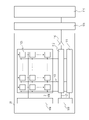
- FIG. 1 is a diagram showing a configuration of a photoelectric conversion device 100 according to an embodiment of the present invention.
- the photoelectric conversion device 100 is a laminated photoelectric conversion device will be described as an example. That is, a photoelectric conversion device configured by stacking two substrates of a sensor substrate 11 and a circuit board 21 and electrically connecting them will be described as an example.
- the photoelectric conversion device is not limited to this.
- it may be a photoelectric conversion device in which the configuration included in the sensor substrate 11 and the configuration included in the circuit board are arranged in a common semiconductor layer, which will be described below.
- the photoelectric conversion device in which the configuration included in the sensor board 11 and the configuration included in the circuit board are arranged in a common semiconductor layer is also referred to as a non-stacked photoelectric conversion device.
- the sensor substrate 11 has a first semiconductor layer having a photoelectric conversion element 102 described later, and a first wiring structure.
- the circuit board 21 has a second semiconductor layer having a circuit such as a signal processing circuit 103 described later, and a second wiring structure.
- the photoelectric conversion device 100 is configured by laminating a second semiconductor layer, a second wiring structure, a first wiring structure, and a first semiconductor layer in this order.
- FIG. 1 illustrates a back-illuminated photoelectric conversion device in which light is incident from the first surface and a circuit board is arranged on the second surface, which is the surface opposite to the first surface.
- the surface on the side where the transistors of the signal processing circuit are arranged is called the second surface.
- the first surface of the semiconductor layer opposite to the second surface is the light incident surface.
- the second surface of the semiconductor layer is the light incident surface.
- each substrate may be a wafer. Further, each substrate may be diced after being laminated in a wafer state, or each chip may be laminated and bonded after being made into chips.
- the pixel area 12 is arranged on the sensor board 11, and the circuit area 22 for processing the signal detected in the pixel area 12 is arranged on the circuit board 21.
- FIG. 2 is a diagram showing an arrangement example of the sensor board 11.
- Pixels 101 having a photoelectric conversion element 102 including an avalanche photodiode (hereinafter referred to as APD) are arranged in a two-dimensional array in a plan view to form a pixel region 12.
- APD avalanche photodiode
- the pixel 101 is typically a pixel for forming an image, but when used for TOF (Time of Flight), it is not always necessary to form an image. That is, the pixel 101 may be a pixel for measuring the time when the light arrives and the amount of light.
- TOF Time of Flight
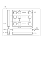
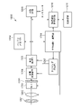
- FIG. 3 is a block diagram of the circuit board 21. It has a signal processing circuit 103, a readout circuit 112, a control pulse generation unit 115, a horizontal scanning circuit unit 111, a signal line 113, and a vertical scanning circuit unit 110 that process the electric charges converted by the photoelectric conversion element 102 of FIG. There is.
- the photoelectric conversion element 102 of FIG. 2 and the signal processing circuit 103 of FIG. 3 are electrically connected via a connection wiring provided for each pixel.
- the vertical scanning circuit unit 110 receives the control pulse supplied from the control pulse generation unit 115 and supplies the control pulse to each pixel.
- a logic circuit such as a shift register or an address decoder is used in the vertical scanning circuit unit 110.
- the control pulse generation unit 115 has a signal generation unit 215 that generates the control signal P_CLK of the switch described later.
- the signal generation unit 215 generates a pulse signal for controlling the switch, as will be described later.
- the signal generation unit 215 may commonly generate a control signal P_CLK for a plurality of pixels in the pixel region, or as shown in FIG. 4B, for each pixel.
- the control signal P_CLK may be generated.
- the pulse signal P_CLK is generated in common, at least one of the period, the number of pulses, and the pulse width of the signal P_EXP pulse signal that controls the exposure period is commonly generated in correspondence with the exposure period.
- control signal P_CLK when the control signal P_CLK is controlled for each pixel, a signal can be generated by using both the input signal P_CLK_IN output from the control pulse generation unit 115 and the signal P_EXP for controlling the exposure period.
- the control pulse generation unit 115 preferably has, for example, a frequency dividing circuit. As a result, it becomes possible to control it simply, and it is possible to reduce the increase in the number of elements.
- the signal output from the photoelectric conversion element 102 of the pixel is processed by the signal processing circuit 103.
- the signal processing circuit 103 is provided with a counter, a memory, and the like, and a digital value is held in the memory.
- the horizontal scanning circuit unit 111 inputs a control pulse for sequentially selecting each column to the signal processing circuit 103 in order to read a signal from the memory of each pixel in which the digital signal is held.
- a signal is output to the signal line 113 from the signal processing circuit 103 of the pixels selected by the vertical scanning circuit unit 110 for the selected column.
- the signal output to the signal line 113 is output to an external recording unit or signal processing unit of the photoelectric conversion device 100 via the output circuit 114.
- the arrangement of the photoelectric conversion elements in the pixel region may be arranged one-dimensionally. Further, it is possible to obtain the effect of the present invention even if there is only one pixel, and the case where there is one pixel is also included in the present invention, but if it is a photoelectric conversion device having a plurality of pixels, the present embodiment It becomes easier to obtain the effect of reducing power consumption.
- the function of the signal processing unit does not necessarily have to be provided for all photoelectric conversion elements one by one. For example, one signal processing unit may be shared by a plurality of photoelectric conversion elements, and signal processing may be sequentially performed.
- a plurality of signal processing circuits 103 are arranged in a region overlapping the pixel region 12 in a plan view. Then, in a plan view, the vertical scanning circuit unit 110, the horizontal scanning circuit unit 111, the readout circuit 112, the output circuit 114, and the control pulse generation unit 115 so as to overlap between the end of the sensor substrate 11 and the end of the pixel region 12. Is arranged. In other words, the sensor substrate 11 has a pixel region 12 and a non-pixel region arranged around the pixel region 12.
- a vertical scanning circuit unit 110, a horizontal scanning circuit unit 111, a readout circuit 112, an output circuit 114, and a control pulse generation unit 115 are arranged in a region overlapping the non-pixel region in a plan view.
- the arrangement of the signal line 113, the reading circuit 112, and the output circuit 114 are not limited to FIG.
- the signal line 113 is arranged so as to extend in the row direction, and the read circuit 112 may be arranged at the destination where the signal line 113 extends.
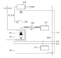
- FIGS. 4A and 4B are examples of block diagrams including the equivalent circuits of FIGS. 2 and 3.
- FIG. 4A is an example in which the signal generation unit 215 is provided in common for a plurality of pixels
- FIG. 4B is an example in which the control signal P_CLK can be controlled for each pixel.
- the photoelectric conversion element 102 having the APD 201 is provided on the sensor board 11, and the other members are provided on the circuit board 21.
- APD201 generates a charge pair according to the incident light by photoelectric conversion.
- One of the two nodes of the APD201 is connected to a power line to which the drive voltage VL (first voltage) is supplied.
- the other node of the two nodes of the APD 201 is connected to a power supply line to which a drive voltage VH (second voltage) higher than the voltage VL supplied to the anode is supplied.
- VL first voltage
- VH second voltage
- a reverse bias voltage is supplied to the anode and cathode of the APD201 so that the APD201 performs an avalanche multiplying operation. By supplying such a voltage, the electric charge generated by the incident light causes an avalanche multiplication, and an avalanche current is generated.
- APD operated in Geiger mode is called SPAD.
- the voltage VL (first voltage) is ⁇ 30V
- the voltage VH (second voltage) is 1V.
- the APD 201 may be operated in the linear mode or the Geiger mode. In the case of SPAD, the potential difference is larger than that of APD in the linear mode, and the effect of withstand voltage becomes remarkable. Therefore, SPAD is preferable.
- the switch 202 is connected to the power supply line to which the drive voltage VH is supplied and to one of the nodes of the anode and cathode of the APD201. Then, the switch 202 switches the resistance value between the APD 201 and the power supply line to which the drive voltage VH is supplied.
- switching the resistance value preferably means changing the resistance value by 10 times or more, and more preferably by changing the resistance value by 100 times or more.
- lowering the resistance value is also referred to as turning on the switch 202
- increasing the resistance value is also referred to as turning off the switch 202.
- the switch 202 functions as a quench element.
- the switch 202 functions as a load circuit (quenching circuit) when the signal is multiplied by the avalanche multiplication, suppresses the voltage supplied to the APD201, and has a function of suppressing the avalanche multiplication (quenching operation). Further, the switch 202 has a function of returning the voltage supplied to the APD 201 to the drive voltage VH by passing a current corresponding to the voltage drop in the quench operation (recharge operation).
- the switch 202 can be configured by, for example, a MOS transistor, and FIGS. 4A and 4B show a case where the switch 202 is a MOSFET transistor.
- the control signal P_CLK of the switch 202 supplied from the signal generation unit 215 is applied to the gate electrode of the MOS transistor constituting the switch 202.
- the on / off of the switch 202 is controlled by controlling the voltage applied to the gate electrode of the switch 202.
- the signal processing circuit 103 has a waveform shaping unit 210, a counter circuit 211, and a selection circuit 212.
- the signal processing circuit 103 has a waveform shaping unit 210, a counter circuit 211, and a selection circuit 212.
- the signal processing circuit 103 includes a waveform shaping unit 210, a counter circuit 211, and It suffices to have at least one of the selection circuits 212.
- the waveform shaping unit 210 shapes the potential change of the cathode of the APD 201 obtained at the time of photon detection, and outputs a pulse signal.
- the node on the input side of the waveform shaping unit 210 is referred to as nodeA, and the node on the output side is referred to as nodeB.
- the waveform shaping unit 210 changes the output potential from the node node B depending on whether the input potential to the node node A is equal to or higher than a predetermined value or lower. For example, in FIG. 5, when the input potential to the node node A becomes a high potential equal to or higher than the determination threshold value, the output potential from the node node B becomes a low level.
- the waveform shaping unit 210 for example, an inverter circuit is used.
- FIGS. 4A and 4B an example in which one inverter is used as the waveform shaping unit 210 is shown, but a circuit in which a plurality of inverters are connected in series may be used, or another circuit having a waveform shaping effect may be used. It is also good.
- the switch 202 It is possible to perform a quench operation and a recharge operation using the switch 202 according to the avalanche multiplication in APD201, but it may not be determined as an output signal depending on the photon detection timing. For example, assume that the avalanche multiplication occurs in APD, the input potential to the node nodeA becomes low level, and the recharge operation is performed. Generally, the determination threshold of the waveform shaping unit 210 is set to a potential higher than the potential difference at which the avalanche multiplication occurs in APD.
- the avalanche multiplication occurs in the APD and the voltage of the nodeA drops. That is, since the potential of nodeA drops at a voltage lower than the determination threshold, the output potential from the node nodeB does not change even though photons are detected. Therefore, even though the avalanche multiplication has occurred, it is not determined as a signal. In particular, under high illuminance, photons enter continuously in a short period of time, which makes it difficult to determine as a signal. As a result, the actual number of incident photons and the output signal tend to deviate from each other despite the high illuminance.
- FIG. 5 describes an example in which the control signal P_CLK is a pulse signal having a repetition period.
- FIG. 5 describes a mode in which the switch 202 is switched on and off at a predetermined clock frequency.
- the effect of suppressing the increase in power consumption of the photoelectric conversion device can be obtained even if the pulse signal is not a signal having a repeating period.
- the counter circuit 211 counts the pulse signal output from the waveform shaping unit 210 and holds the count value. Further, when the control pulse pRES is supplied via the drive line 213, the signal held in the counter circuit 211 is reset.
- a control pulse pSEL is supplied to the selection circuit 212 from the vertical scanning circuit unit 110 of FIG. 3 via the drive lines 214 (not shown in FIG. 3) of FIGS. 4A and 4B, and the counter circuit 211 and the signal line 113 are supplied. Switch between electrical connection and disconnection.
- the selection circuit 212 includes, for example, a buffer circuit for outputting a signal.
- the output signal OUT shown in FIGS. 4A and 4B is a signal output from the pixel.
- a switch such as a transistor may be arranged between the switch 202 and the APD 201 or between the photoelectric conversion element 102 and the signal processing circuit 103 to switch the electrical connection.
- the supply of the voltage VH or the voltage VL supplied to the photoelectric conversion element 102 may be electrically switched by using a switch such as a transistor.
- a photoelectric conversion device 100 that acquires a pulse detection timing may be used by using a time / digital conversion circuit (Time to Digital Converter: hereinafter, TDC) and a memory.
- TDC Time to Digital Converter
- a control pulse pREF reference signal
- the TDC acquires a signal as a digital signal when the input timing of the signal output from each pixel via the waveform shaping unit 210 is set to a relative time with the control pulse pREF as a reference.
- the signal generation unit 215 may be provided for each pixel.
- the circuit after the waveform shaping unit 210 shown in FIG. 4A and the figure of the signal generation unit are omitted. It is assumed that the signal generation unit 215 of FIG. 4A is located for each pixel.
- FIG. 4B takes a logic circuit in the pixel and determines whether or not to supply a pulse signal to the switch 202.
- the signal P_EXP for controlling the exposure period and the input signal P_CLK_IN for controlling the control signal P_CLK are input to the logic circuit. Then, the signal to be inverted is output.
- the switch when the signal P_EXP for controlling the exposure period is low level and the input signal P_CLK_IN is low level, a high level signal is output from the control signal P_CLK. That is, the switch is turned off. Further, when the signal P_EXP for controlling the exposure period is high level and the input signal P_CLK_IN is high level, a low level signal is output from the control signal P_CLK. That is, the switch is turned on. Further, when one of the signal P_EXP for controlling the exposure period and the input signal P_CLK_IN is low level, a high level signal is output as the control signal P_CLK. That is, the switch 202 is turned off. It is preferable to control the switch for each pixel in this way. When the circuit diagram of FIG. 4B is used, the control signal P_CLK is maintained at a high level when the exposure period P becomes a low level, as will be described in the second embodiment described later. That is, the switch is turned off.
- FIG. 5 is a diagram schematically showing the relationship between the switch control signal P_CLK, the potential of the node nodeA, the potential of the node nodeB, and the output signal.
- the control signal P_CLK when the control signal P_CLK is at a high level, the drive voltage VH is difficult to be supplied to the APD, and when the control signal P_CLK is at a low level, the drive voltage VH is supplied to the APD.
- the high level of the control signal P_CLK is, for example, 1V
- the low level of the control signal P_CLK is, for example, 0V.
- the resistance value of the switch when the control signal P_CLK is high level is higher than the resistance value of the switch when the control signal P_CLK is low level.
- the control signal P_CLK is at a high level, the recharge operation is difficult to be performed even if the avalanche multiplication occurs in the APD, so that the potential supplied to the APD becomes a potential equal to or lower than the breakdown voltage of the APD. Therefore, the avalanche multiplication operation in APD is stopped.
- the switch 202 is composed of one transistor, and the quench operation and the recharge operation are performed by one transistor. This makes it possible to reduce the number of circuits as compared with the case where the quench operation and the recharge operation are performed by different circuit elements.
- the switch 202 is configured by one transistor. The effect of this becomes remarkable.
- the control signal P_CLK changes from high level to low level
- the switch is turned on, and the APD recharge operation is started.
- the potential of the cathode of the APD transitions to a high level.
- the potential difference between the potentials applied to the anode and the cathode of the APD becomes a state in which the avalanche can be multiplied.
- the potential of the cathode is the same as that of the node nodeA. Therefore, when the potential of the cathode changes from the low level to the high level, the potential of the node nodeA becomes equal to or higher than the determination threshold value at time t2.
- the pulse signal output from the node nodeB is inverted and changes from high level to low level.
- the potential difference between the drive voltage VH and the drive voltage VL is applied to the APD201.
- the control signal P_CLK becomes high level and the switch is turned off.
- the portion of the node nodeA where the output waveform exceeds the determination threshold is waveform-shaped by the waveform shaping unit 210 and output as a signal by the nodeB. Then, the count value of the counter signal counted by the counter circuit and output from the counter circuit is increased by 1 LSB.
- a photon is incident on the APD between time t3 and time t4, but the switch is off and the voltage applied to the APD201 is not a potential difference that can be multiplied by the avalanche, so the voltage level of the node nodeA is Do not exceed the judgment threshold.
- the control signal P_CLK changes from high level to low level, and the switch is turned on. Along with this, a current that compensates for the voltage drop flows from the drive voltage VL to the node nodeA, and the voltage of the node nodeA transitions to the original voltage level. At this time, since the voltage of the node node A becomes equal to or higher than the determination threshold value at time t5, the pulse signal of the node node B is inverted and changes from high level to low level.
- the node nodeA statically determinates to the original voltage level, and the control signal P_CLK changes from low level to high level. Therefore, the switch is turned off. Even after that, as described from time t1 to time t6, the potentials of each node, signal line, and the like change according to the incident of the control signal P_CLK and photons.
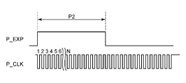
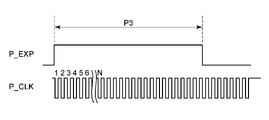
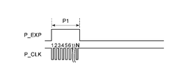
- FIG. 6A to 6C are timing charts showing the relationship between the exposure period P and the control signal P_CLK in the first embodiment.
- FIG. 6A is a diagram showing a pulse signal of the control signal P_CLK in the case of the exposure period P1.
- FIG. 6B is a diagram showing a pulse signal of the control signal P_CLK in the case of an exposure period P2 having an exposure period longer than the exposure period P1.
- FIG. 6C is a diagram showing a pulse signal of the control signal P_CLK in the case of an exposure period P3 having an exposure period longer than the exposure period P2.
- the exposure period P is, for example, a period in which the mechanical shutter or the electronic shutter is open, and the non-exposure period is, for example, a period in which the mechanical shutter or the electronic shutter is closed.
- the exposure period P may be defined by adjusting the bias applied to the APD 201 to change whether or not the photon signal can be acquired.
- the exposure period P refers to a period in which the APD 201 is operable and the APD and the signal processing circuit can read the signal.
- the state in which the APD and the signal processing circuit can read the signal means a state in which the APD can multiply the avalanche. During this time, it can be said that the counter circuit is in operation.
- the period of the quenching operation of the APD which is a state of being turned off based on the incident of photons, becomes a part of the operable state.
- the period in which the light is shielded by a shutter or the like or the period in which the APD is controlled so as not to multiply the avalanche regardless of the presence or absence of photons is a non-exposure period.
- the pulse signal of the control signal P_CLK is changed according to the exposure period P. It is assumed that the second exposure period is different from the first exposure period and the first exposure period.
- the first exposure period is divided by the number of control signals P_CLK in the first exposure period divided by the first exposure period and multiplied by the first exposure period, and the number of control signals P_CLK in the second exposure period is divided by the second exposure period.
- the control signal is controlled so that it differs from the value obtained by multiplying the exposure period. Since the switch 202 is a polyclonal transistor in this embodiment, the number of control signals P_CLK refers to the number of pulse offs within a predetermined exposure period.
- the control signal P_CLK when compared per unit time, is different so that the average frequency of the control signal P_CLK in the first exposure period and the average frequency of the control signal P_CLK in the second exposure period different from the first exposure period are different.
- the average frequency of the control signal P_CLK in the exposure period refers to the frequency obtained by averaging the pulse signals in the exposure period so as to be uniform. For example, if the pulse signals are densely distributed in the first half of the exposure period and no pulse signals are distributed in the second half, the frequency adjusted so that the pulse signals are distributed evenly throughout the period is exposed. It is called the average frequency of the control signal P_CLK during the period. Then, in the present embodiment, when the average frequency is compared between the first exposure period and the second exposure period, the average frequency is controlled to be different.
- the unit time is a time during which at least two pulse signals of the control signal P_CLK are input.
- the pulse signal of the control signal P_CLK is controlled so that the number of pulses of the pulse signal in the exposure period P is the same even if the exposure period P changes. It is assumed that the number of pulses of the control signal P_CLK in the exposure period P1 shown in FIG. 6A is N. Even in the exposure period P2 shown in FIG. 6B, the number of pulses of the control signal P_CLK is set to N. Further, even in the exposure period P3 shown in FIG. 6C, the number of pulses of the control signal P_CLK is set to N.
- FIGS. 7A to 7C are timing charts showing the relationship between the exposure period P and the control signal P_CLK in the comparative mode.
- FIGS. 7A to 7C the same configurations as those in FIGS. 6A to 6C are designated by the same reference numerals as those in FIGS. 6A to 6C, and the description thereof will be omitted.
- the cycle of the control signal P_CLK is the same even if the exposure period changes.
- the period of the control signal P_CLK refers to the period from the fall of the pulse to the next fall.
- the period of the control signal P_CLK is the same in both the exposure period P1 and the exposure period P2. Therefore, in the comparative mode, when the exposure period P changes, the number of pulses of the pulse signal in the exposure period P changes. In this form, the power consumption may be unintentionally increased depending on the exposure period.
- the signal processing circuit in the subsequent stage even if the clock frequency increases, the result is not reflected, and there is a possibility that wasteful power consumption is consumed.
- the signal processing circuit is a counter circuit
- the clock frequency at a value larger than the readable upper limit of the counter is not read as a signal. That is, if the value is larger than the upper limit of the counter, the count value is not added by the counter circuit even if the quench operation and the recharge operation are performed to read the signal. Therefore, wasteful power consumption occurs at a value larger than the counter upper limit value.
- the clock frequency is set too high, the number of photons that can be read out decreases, and the dynamic range may decrease.
- wasteful power consumption can be reduced by controlling the number of pulses of the pulse signal of the control signal P_CLK according to the exposure period.
- the cycle of the control signal P_CLK changes according to the exposure period.
- the period of the control signal P_CLK in the exposure period P1 is shorter than the cycle of the control signal P_CLK in the exposure period P2.
- the number of pulses of the control signal P_CLK is always N times even if the exposure period changes as in the exposure period P1, the exposure period P2, and the exposure period P3. .. This makes it possible to reduce the increase in power consumption.
- the number of pulses during the exposure period can be set to any value.
- the signal processing circuit in the subsequent stage is a counter circuit, it is preferable to set the count upper limit value of the counter circuit, for example. As a result, it is possible to suppress the generation of unnecessary power consumption while suppressing the decrease in the dynamic range.
- the first pulse width in the exposure period P1 and the first pulse width in the exposure period P2 are the same.
- the first pulse width refers to the period during which the switch 202 is turned on by the control signal P_CLK.
- the switch 202 since the switch 202 is a polyclonal transistor, the first pulse width refers to a period in which the control signal P_CLK is at a low level (first level).
- first level the control signal P_CLK is at the high level (second level)
- the switch is turned off and the recharge operation is difficult to be performed by the APD.
- the period during which the control signal P_CLK maintains the state of the first level is described as “the first pulse width”
- the period during which the control signal P_CLK maintains the state of the second level is described. It is called “second pulse width”.
- the first pulse width in the exposure period P1 and the first pulse width in the exposure period P2 are the same, but the second pulse width in the exposure period P1 and the second pulse width in the exposure period P2. It is different from the pulse width of.
- the switch is turned on and the recharge operation is performed by APD. If the low level period of the control signal P_CLK becomes long, the recharge operation may be performed a plurality of times. As described with reference to FIG. 5, there is a possibility that the potential of the node node A drops when the potential of the node node A is lower than the determination threshold value, the signal of the node B is not inverted, and the signal value cannot be read properly. be.
- the period during which the recharge operation is performed by the APD is set to a fixed period, so that the recharge operation is not performed a plurality of times during the low level period of the control signal P_CLK, and photon detection omission is prevented. Can be reduced.
- FIG. 8 is an example of a flowchart of the operation of the photoelectric conversion device in this embodiment.
- step S1 the exposure period and the number of pulses of the control signal P_CLK are set.
- the clock frequency of the control signal P_CLK is set.
- Shooting is started in step S2.
- step S3 it is decided whether or not to change the exposure period. Whether or not to change the exposure period can be determined by judging from the information obtained from the image taken before that (information in the previous frame). If the information obtained from the image in the previous frame is too bright, the exposure period is shortened, and if the information obtained from the image is too dark, the exposure period is lengthened. In addition to this, the exposure period can be switched manually or automatically.
- step S4 When changing in step S3, it is determined in step S4 whether or not to lengthen the exposure period setting. If it is determined in step S3 that the exposure period is to be changed, the process proceeds to step S4, and if it is determined in step 3 that the exposure period is not changed, the process proceeds to step S.
- step S4 When it is determined in step S4 that the setting of the exposure period is lengthened, the average clock frequency of the control signal P_CLK within the exposure period is lowered in step S5. At this time, the number of pulses of the control signal P_CLK during the exposure period is controlled so as not to change before and after the exposure period is changed.
- step S4 the setting of the exposure period is not lengthened (shortened)
- the average clock frequency of the control signal P_CLK within the exposure period is set high in step S6. Even in this case, the number of pulses of the control signal P_CLK before the exposure period is changed and the number of pulses of the control signal P_CLK during the exposure period are controlled so as not to change.
- step S5 or step S6 the process proceeds to step S7 to determine whether or not to end the shooting. If it is determined that the exposure period ends in step S7, shooting ends in step S8. If it is determined that the shooting is not completed in step S7, the process returns to step S3, and steps S3 to S7 are repeated. Then, if it is determined that the shooting is finished in step S7, the shooting is finished in step S8.
- FIGS. 9A to 9F show modified examples of the timing chart.
- the pulse signal P_CLK is input at regular intervals, but the present invention is not limited to this.
- the pulse signal P_CLK may be input while changing the pulse period. Although the period is changed for each pulse signal in FIGS. 9A to 9C, the period may be changed for each of three or four or more pulse signals.
- the number of pulses in the exposure period P2 and the number of pulses in the exposure period P3 may be the same as the number of pulses in the exposure period P1 in the same period as the exposure period P1. That is, the control signal P_CLK may be continuously supplied to the switch in the first half of the exposure period P2, and the control signal P_CLK may not be supplied in the latter half of the exposure period P2. Even in such a case, if the number of pulses in the exposure period P2 and the number of pulses in the exposure period P1 are the same, the effect of the present embodiment can be obtained. Similarly, if the number of pulses in the exposure period P3 and the number of pulses in the exposure period P1 are the same, the effect of the present embodiment can be obtained.
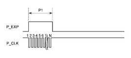
- FIG. 10A to 10C are timing charts showing the relationship between the exposure period P and the control signal P_CLK in the second embodiment.
- FIG. 10A is a diagram showing a pulse of the control signal P_CLK in the case of the exposure period P1.
- FIG. 10B is a diagram showing a pulse signal of the control signal P_CLK in the case of an exposure period P2 having an exposure period longer than the exposure period P1.
- FIG. 10C is a diagram showing a pulse signal of the control signal P_CLK in the case of an exposure period P3 longer than the exposure period P2.
- the photoelectric conversion device of the present embodiment is different from the first embodiment in that the pulse signal of the control signal P_CLK is not generated at the timing when the exposure period changes to the non-exposure period. Except for this point and the matters described below, the configuration is substantially the same as that of the first embodiment. Therefore, the same reference numerals may be given to the same configurations as those of the first embodiment, and the description may be omitted.
- control signal P_CLK is stopped at a low level at the end timing of the exposure period. That is, it leaves the switch off. Then, the control signal P_CLK is changed to a high level at the start timing of the exposure period.
- the end timing of the exposure period may be controlled so as to be synchronized with the shutter.
- the present embodiment can also suppress the increase in power consumption as in the first embodiment. Further, since the number of times the switch is turned on and off can be reduced as compared with the first embodiment, the power consumption of the photoelectric conversion device can be further suppressed.
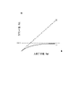
- FIG. 11 is a diagram showing the relationship between the number of incident photons Nph in each pixel of the photoelectric conversion device and the count value Nct.
- Nph is the number of photons actually incident on each pixel (number of incident photons) per exposure period T.
- Nct is a count value of the pulse signal output from the waveform shaping unit 210, which is counted by the counter circuit 211.
- the frequency of P_CLK is f
- the number of pulses of P_CLK within the exposure period T is equal to f ⁇ T.
- the count value Nct of each pixel has the characteristics as shown in the curve A in FIG. That is, the count value Nct increases as the number of incident photons Nph increases, and is counted with the number of pulses f ⁇ T as the upper limit. Since the recharge operation is once for each P_CLK pulse, only one photon can be counted per P_CLK cycle. Therefore, when a plurality of photons are incident in one P_CLK cycle, the second and subsequent photons in each cycle are not counted. Therefore, in a high illuminance environment, the number of photons that are not counted even if they are incident on the pixel increases, and the count value Nct and the actual number of incident photons Nph deviate from each other.
- correction is performed to convert the count value Nct to the actual number of incident photons Nph.
- This correction is performed by the correction circuit 118 connected to the circuit board 21.
- the correction circuit 118 may be outside the photoelectric conversion unit 100 or inside the photoelectric conversion unit 100 (for example, the signal processing circuit 103).
- 119 in FIG. 12 is an external output circuit.
- Nct f ⁇ T ⁇ (1-exp (-Nph / (f ⁇ T)) Equation (1)
- this correction circuit 118 when the count value Nct, the frequency f of the pulse signal, and the length T of the exposure period are used as explanatory variables, and the number of incident photons Nph is used as the objective variable, the explanatory variables and the objective variables are used. Is described by a relational expression based on the natural logarithm.
- the corrected count value Nct can be represented by the dotted line B in FIG.
- the count value of A which has a non-linear characteristic with respect to the number of incident photons, can be corrected to the count value of B, which corresponds to the number of incident photons having linearity.
- the correction formula is determined by the value of f ⁇ T, even if the value of the exposure period T is determined for each of the different P_CLK frequencies f, as long as the combination is such that f ⁇ T is constant, the number of incident photons Nph. The value of the count value Nct for is unchanged.
- Nct f 1 x T 1 x (1-exp (-Nph 1 / (f 1 x T 1 ))) + f 2 x T 2 x (1-exp (-Nph 2 / (f 2 x T 2 )))) Equation (2)
- T 1 is a period in which the pulse signal operates at the first frequency f 1
- T 2 is a period in which the pulse signal operates at the second frequency f 2
- T 1 + T 2 is an exposure period T.
- Nph 1 is the number of incident photons at T 1
- Nph 2 is the number of incident photons at T 2 .
- Nph 2 Nph ⁇ T 2 / (T 1 + T 2 ) Equation (4)
- the number of incident photons is determined by the ratio of the exposure period at each frequency to the total exposure period T.
- FIGS. 13A and 13B show a case where a plurality of frequencies coexist within the exposure period as shown in FIGS. 13A and 13B.
- the pulse signals are collectively input for each frequency so that the frequency of the pulse signal input in the first half of the exposure period is f1 and the frequency of the pulse signal input in the second half is f2. May be done.
- two pulses having different frequencies may be alternately continued, and pulse signals having a frequency f 1 and a frequency f 2 may be alternately continued one pulse at a time.
- FIGS. 13A and 13B show an example in which pulse signals having two kinds of frequencies are mixed in the exposure period, pulse signals having three or more kinds of frequencies may be mixed.
- the slope of the count value at high illuminance becomes larger than when only low frequency pulse signals are input. Therefore, the toneability of the count value is maintained even in high illuminance, and the dynamic range can be expanded as compared with the case where the frequency of the pulse signal is one type.
- n a natural number of 2 or more.
- Nct f 1 x T 1 x (1-exp (-Nph 1 / (f 1 x T 1 ))) + f 2 x T 2 x (1-exp (-Nph 2 / (f 2 x T 2 )))) + ...
- Nph 1 Nph ⁇ T 1 / (T 1 + T 2 + ... + T n-1 + T n ) Equation (6)
- Nph 2 Nph ⁇ T 2 / (T 1 + T 2 + ... + T n-1 + T n ) Equation (7)
- Nph n-1 Nph ⁇ T n-1 / (T 1 + T 2 + ... + T n-1 + T n ) Equation (8)
- Nph n Nph ⁇ T n / (T 1 + T 2 + ... + T n-1 + T n ) Equation (9)
- the number of incident photons is determined by the ratio of the exposure period at each frequency to the total exposure period T.
- the correction performed by the correction circuit 118 is not limited to the case where the correction by the above formula is performed for each count value each time.
- the correction circuit 118 may have a three-dimensional table of a combination of an exposure period T, a pulse signal frequency f, and a count value Nct.
- the number of incident photons Nph can be estimated by selecting the value closest to the measured value from the numerical values in the table of the correction circuit 118.
- the numerical values in the table are set by the relational expression based on the natural logarithm according to the combination of f and T as in the above expression.
- the correction for the count value is not limited to this, and the correction step may be reduced by performing other corrections at the same time as the main correction in the correction circuit 118.
- so-called gamma correction may be performed to adjust the brightness of the image formed based on the count value.
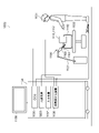
- FIG. 14 is a block diagram showing the configuration of the photodetection system 1200 according to the present embodiment.
- the photodetector system 1200 of this embodiment includes a photoelectric conversion device 1204.
- the photoelectric conversion device 1204 any of the photoelectric conversion devices described in the above-described embodiment can be applied.
- the photodetection system 1200 can be used, for example, as an imaging system. Specific examples of the imaging system include a digital still camera, a digital camcorder, a surveillance camera, and the like.
- FIG. 14 shows an example of a digital still camera as a photodetection system 1200.
- the light detection system 1200 shown in FIG. 1 includes a photoelectric conversion device 1204, a lens 1202 for forming an optical image of a subject on the photoelectric conversion device 1204, a throttle 1203 for varying the amount of light passing through the lens 1202, and protection of the lens 1202. Has a barrier 1201 for.
- the lens 1202 and the aperture 1203 are optical systems that condense light on the photoelectric conversion device 1204.
- a shutter is arranged between the aperture 1203 and the photoelectric conversion device 1204. The exposure period of the photoelectric conversion device is controlled by opening and closing the shutter.
- the optical detection system 1200 has a signal processing unit 1205 that processes an output signal output from the photoelectric conversion device 1204.
- the signal processing unit 1205 performs a signal processing operation of performing various corrections and compressions on the input signal as necessary and outputting the signal.
- the optical detection system 1200 further includes a buffer memory unit 1206 for temporarily storing image data, and an external interface unit (external I / F unit) 1209 for communicating with an external computer or the like.
- the optical detection system 1200 includes a recording medium 1211 such as a semiconductor memory for recording or reading imaging data, and a recording medium control interface unit (recording medium control I / F unit) for recording or reading on the recording medium 1211.
- the recording medium 1211 may be built in the photodetection system 1200 or may be removable. Further, communication from the recording medium control I / F unit 1210 to the recording medium 1211 and communication from the external I / F unit 1209 may be performed wirelessly.
- the optical detection system 1200 has a general control / calculation unit 1208 that performs various calculations and controls the entire digital still camera, and a timing generation unit 1207 that outputs various timing signals to the photoelectric conversion device 1204 and the signal processing unit 1205.
- a timing signal or the like may be input from the outside, and if the optical detection system 1200 has at least a photoelectric conversion device 1204 and a signal processing unit 1205 that processes an output signal output from the photoelectric conversion device 1204. good.
- the timing generator 1207 may be mounted on the photoelectric conversion device.
- the overall control / calculation unit 1208 and the timing generation unit 1207 may be configured to perform part or all of the control functions of the photoelectric conversion device 1204.
- the photoelectric conversion device 1204 outputs an image signal to the signal processing unit 1205.
- the signal processing unit 1205 performs predetermined signal processing on the image signal output from the photoelectric conversion device 1204, and outputs the image data. Further, the signal processing unit 1205 uses the image signal to generate an image. Further, the signal processing unit 1205 may perform a distance measuring operation on the signal output from the photoelectric conversion device 1204.
- the signal processing unit 1205 and the timing generation unit 1207 may be mounted on the photoelectric conversion device. That is, the signal processing unit 1205 and the timing generation unit 1207 may be provided on the substrate on which the pixels are arranged, or may be provided on another substrate.
- FIG. 15 is a block diagram showing a configuration example of a distance image sensor, which is an electronic device using the photoelectric conversion device described in the above-described embodiment.
- the distance image sensor 401 includes an optical system 407, a photoelectric conversion device 408, an image processing circuit 404, a monitor 405, and a memory 406. Then, the distance image sensor 401 receives light (modulated light or pulsed light) that is projected from the light source device 409 toward the subject and reflected on the surface of the subject, so that the distance image corresponds to the distance to the subject. Can be obtained.
- light modulated light or pulsed light
- the optical system 407 is configured to have one or a plurality of lenses, guides image light (incident light) from a subject to a photoelectric conversion device 408, and forms an image on a light receiving surface (sensor unit) of the photoelectric conversion device 408. Let me.
- the photoelectric conversion device 408 the photoelectric conversion device of each of the above-described embodiments is applied, and a distance signal indicating a distance obtained from a light receiving signal output from the photoelectric conversion device 408 is supplied to the image processing circuit 404.
- the image processing circuit 404 performs image processing for constructing a distance image based on the distance signal supplied from the photoelectric conversion device 408. Then, the distance image (image data) obtained by the image processing is supplied to the monitor 405 and displayed, or supplied to the memory 406 and stored (recorded).
- the distance image sensor 401 configured in this way, by applying the above-mentioned photoelectric conversion device, for example, a more accurate distance image can be acquired as the characteristics of the pixels are improved.
- the technique according to the present disclosure (the present technique) can be applied to various products.
- the techniques according to the present disclosure may be applied to an endoscopic surgery system.
- FIG. 16 is a diagram showing an example of a schematic configuration of an endoscopic surgery system to which the technique according to the present disclosure (the present technique) can be applied.
- FIG. 16 illustrates how the surgeon (doctor) 1131 is performing surgery on patient 1132 on patient bed 1133 using the endoscopic surgery system 1003.
- the endoscopic surgery system 1003 includes an endoscope 1100, a surgical tool 1110, and a cart 1134 equipped with various devices for endoscopic surgery.
- the endoscope 1100 is composed of a lens barrel 1101 in which a region having a predetermined length from the tip is inserted into the body cavity of the patient 1132, and a camera head 1102 connected to the base end of the lens barrel 1101.
- the endoscope 1100 configured as a so-called rigid mirror having a rigid barrel 1101 is illustrated, but the endoscope 1100 may be configured as a so-called flexible mirror having a flexible barrel. good.
- the tip of the lens barrel 1101 is provided with an opening in which an objective lens is fitted.
- a light source device 1203 is connected to the endoscope 1100, and the light generated by the light source device 1203 is guided to the tip of the lens barrel by a light guide extending inside the lens barrel 1101 to be an objective lens. It is irradiated toward the observation target in the body cavity of the patient 1132.
- the endoscope 1100 may be a direct endoscope, a perspective mirror, or a side endoscope.
- An optical system and a photoelectric conversion device are provided inside the camera head 1102, and the reflected light (observation light) from the observation target is focused on the photoelectric conversion device by the optical system.
- the observation light is photoelectrically converted by the photoelectric conversion device, and an electric signal corresponding to the observation light, that is, an image signal corresponding to the observation image is generated.
- the photoelectric conversion device the photoelectric conversion device described in each of the above-described embodiments can be used.
- the image signal is transmitted as RAW data to the camera control unit (CCU: Camera Control Unit) 1135.
- the CCU 1135 is composed of a CPU (Central Processing Unit), a GPU (Graphics Processing Unit), and the like, and comprehensively controls the operations of the endoscope 1100 and the display device 1136. Further, the CCU 1135 receives an image signal from the camera head 1102, and performs various image processing such as development processing (demosaic processing) on the image signal to display an image based on the image signal.
- image processing such as development processing (demosaic processing)
- the display device 1136 displays an image based on the image signal processed by the CCU 1135 under the control of the CCU 1135.
- the light source device 1203 is composed of, for example, a light source such as an LED (Light Emitting Diode), and supplies irradiation light for photographing an operating part or the like to the endoscope 1100.
- a light source such as an LED (Light Emitting Diode)
- LED Light Emitting Diode
- the input device 1137 is an input interface for the endoscopic surgery system 1003.
- the user can input various information and input instructions to the endoscopic surgery system 1003 via the input device 1137.
- the treatment tool control device 1138 controls the drive of the energy treatment tool 1112 for cauterizing, incising, sealing blood vessels, and the like.
- the light source device 1203 that supplies the irradiation light for photographing the surgical site to the endoscope 1100 can be composed of, for example, an LED, a laser light source, or a white light source composed of a combination thereof.
- a white light source is configured by a combination of RGB laser light sources, the output intensity and output timing of each color (each wavelength) can be controlled with high accuracy. Therefore, the light source device 1203 adjusts the white balance of the captured image. It can be carried out.
- the laser light from each of the RGB laser light sources is irradiated to the observation target in a time-division manner, and the drive of the image sensor of the camera head 1102 is controlled in synchronization with the irradiation timing to correspond to each of RGB. It is also possible to capture the image in a time-division manner. According to this method, a color image can be obtained without providing a color filter in the image pickup device.
- the drive of the light source device 1203 may be controlled so as to change the intensity of the output light at predetermined time intervals.
- the drive of the image sensor of the camera head 1102 in synchronization with the timing of the change of the light intensity to acquire an image in time division and synthesizing the image, so-called high dynamic without blackout and overexposure. Range images can be generated.
- the light source device 1203 may be configured to be able to supply light in a predetermined wavelength band corresponding to special light observation.
- Special light observation utilizes, for example, the wavelength dependence of light absorption in body tissues. Specifically, by irradiating a narrow band of light as compared with the irradiation light (that is, white light) at the time of normal observation, a predetermined tissue such as a blood vessel on the surface layer of the mucous membrane is photographed with high contrast.
- fluorescence observation may be performed in which an image is obtained by fluorescence generated by irradiating with excitation light.
- the body tissue is irradiated with excitation light to observe the fluorescence from the body tissue, or a reagent such as indocyanine green (ICG) is locally injected into the body tissue and the fluorescence wavelength of the reagent is injected into the body tissue. It is possible to obtain a fluorescence image by irradiating the excitation light corresponding to the above.
- the light source device 1203 may be configured to be capable of supplying narrowband light and / or excitation light corresponding to such special light observation.
- FIGS. 17A, 17B and 18 are schematic views showing a configuration example of a photodetection system and a moving body according to the present embodiment.
- FIG. 18 is a flow chart showing the operation of the photodetection system according to the present embodiment.
- an example of an in-vehicle camera is shown as an optical detection system.
- FIGS. 17A and 17B show an example of a vehicle system and an optical detection system for imaging mounted on the vehicle system.
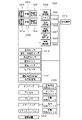
- the optical detection system 1301 includes a photoelectric conversion device 1302, an image preprocessing unit 1315, an integrated circuit 1303, and an optical system 1314.
- the optical system 1314 forms an optical image of a subject on the photoelectric conversion device 1302.
- the photoelectric conversion device 1302 converts the optical image of the subject imaged by the optical system 1314 into an electric signal.
- the photoelectric conversion device 1302 is a photoelectric conversion device according to any one of the above-described embodiments.
- the image preprocessing unit 1315 performs predetermined signal processing on the signal output from the photoelectric conversion device 1302. The function of the image preprocessing unit 1315 may be incorporated in the photoelectric conversion device 1302.
- the optical detection system 1301 is provided with at least two sets of an optical system 1314, a photoelectric conversion device 1302, and an image preprocessing unit 1315, and the output from each set of image preprocessing units 1315 is input to the integrated circuit 1303. It has become like.
- the integrated circuit 1303 is an integrated circuit for an imaging system application, and includes an image processing unit 1304 including a memory 1305, an optical distance measuring unit 1306, a distance measuring calculation unit 1307, an object recognition unit 1308, and an abnormality detection unit 1309.
- the image processing unit 1304 performs image processing such as development processing and defect correction on the output signal of the image preprocessing unit 1315.
- the memory 1305 stores the primary storage of the captured image and the defect position of the captured pixel.
- the optical ranging unit 1306 focuses the subject and measures the distance.
- the distance measurement calculation unit 1307 calculates distance measurement information from a plurality of image data acquired by the plurality of photoelectric conversion devices 1302.
- the object recognition unit 1308 recognizes a subject such as a car, a road, a sign, or a person.
- the abnormality detection unit 1309 detects an abnormality in the photoelectric conversion device 1302, the abnormality detection unit 1309 notifies the main control unit 1313 of the abnormality.
- the integrated circuit 1303 may be realized by hardware specially designed, may be realized by a software module, or may be realized by a combination thereof. Further, it may be realized by FPGA (Field Programmable Gate Array), ASIC (Application Specific Integrated Circuit), or the like, or may be realized by a combination thereof.
- FPGA Field Programmable Gate Array
- ASIC Application Specific Integrated Circuit
- the main control unit 1313 controls and controls the operations of the photodetection system 1301, the vehicle sensor 1310, the control unit 1320, and the like. There is also a method in which the optical detection system 1301, the vehicle sensor 1310, and the control unit 1320 each have a communication interface individually without having a main control unit 1313, and each of them sends and receives a control signal via a communication network (for example, CAN standard). It can be taken.
- a communication network for example, CAN standard
- the integrated circuit 1303 has a function of receiving a control signal from the main control unit 1313 or transmitting a control signal and a set value to the photoelectric conversion device 1302 by its own control unit.
- the light detection system 1301 is connected to the vehicle sensor 1310 and can detect the vehicle running state such as vehicle speed, yaw rate, steering angle, the environment outside the vehicle, and the state of other vehicles / obstacles.
- the vehicle sensor 1310 is also a distance information acquisition means for acquiring distance information to an object.
- the optical detection system 1301 is connected to a driving support control unit 1311 that provides various driving support such as automatic steering, automatic cruising, and collision prevention function.
- collision estimation / collision presence / absence with other vehicles / obstacles is determined based on the detection results of the light detection system 1301 and the vehicle sensor 1310. As a result, avoidance control when a collision is estimated and safety device activation in the event of a collision are performed.
- the light detection system 1301 is also connected to an alarm device 1312 that issues an alarm to the driver based on the determination result in the collision determination unit. For example, when the possibility of a collision is high as the judgment result of the collision determination unit, the main control unit 1313 controls the vehicle to avoid the collision and reduce the damage by applying the brake, releasing the accelerator, suppressing the engine output, and the like. conduct.
- the alarm device 1312 warns the user by sounding an alarm such as a sound, displaying alarm information on a display unit screen of a car navigation system, a meter panel, or the like, or giving vibration to a seat belt or steering.
- FIG. 17B shows an arrangement example of the photodetection system 1301 when the front of the vehicle is imaged by the photodetection system 1301.
- the two photoelectric conversion devices 1302 are arranged in front of the vehicle 1300. Specifically, when the center line with respect to the advancing / retreating direction or the outer shape (for example, the vehicle width) of the vehicle 1300 is regarded as an axis of symmetry, and the two photoelectric conversion devices 1302 are arranged line-symmetrically with respect to the axis of symmetry, the vehicle 1300 and It is preferable for acquiring distance information with the object to be photographed and determining the possibility of collision. Further, it is preferable that the photoelectric conversion device 1302 is arranged so as not to obstruct the driver's field of view when the driver visually recognizes the situation outside the vehicle 1300 from the driver's seat.
- the alarm device 1312 is preferably arranged so that it can be easily seen by the driver.
- the failure detection operation of the photoelectric conversion device 1302 in the photodetection system 1301 will be described with reference to FIG.
- the failure detection operation of the photoelectric conversion device 1302 is performed according to steps S1410 to S1480 shown in FIG.
- Step S1410 is a step for setting the photoelectric conversion device 1302 at the time of startup. That is, the setting for the operation of the photoelectric conversion device 1302 is transmitted from the outside of the light detection system 1301 (for example, the main control unit 1313) or the inside of the light detection system 1301, and the imaging operation and the failure detection operation of the photoelectric conversion device 1302 are performed. Start.
- step S1420 a pixel signal is acquired from the effective pixel. Further, in step S1430, the output value from the failure detection pixel provided for failure detection is acquired.
- the failure detection pixel includes a photoelectric conversion element like the effective pixel. A predetermined voltage is written in this photoelectric conversion element. The failure detection pixel outputs a signal corresponding to the voltage written in the photoelectric conversion element.
- the steps S1420 and S1430 may be reversed.
- step S1440 the non-determination of the expected output value of the failure detection pixel and the output value from the actual failure detection pixel is performed. If the expected output value and the actual output value match as a result of the non-determination in step S1440, the process proceeds to step S1450, it is determined that the imaging operation is normally performed, and the processing step proceeds to step S1460. And migrate. In step S1460, the pixel signal of the scanning line is transmitted to the memory 1305 and primarily stored. After that, the process returns to step S1420 and the failure detection operation is continued. On the other hand, if the expected output value and the actual output value do not match as a result of the non-determination in step S1440, the processing step proceeds to step S1470.
- step S1470 it is determined that there is an abnormality in the imaging operation, and an alarm is issued to the main control unit 1313 or the alarm device 1312.
- the alarm device 1312 causes the display unit to display that an abnormality has been detected.
- step S1480 the photoelectric conversion device 1302 is stopped, and the operation of the photodetection system 1301 is terminated.
- the flowchart may be looped for each of a plurality of lines, or the failure detection operation may be performed for each frame.
- the alarm issued in step S1470 may be notified to the outside of the vehicle via the wireless network.
- the control that does not collide with other vehicles has been described, but it can also be applied to the control that automatically drives following other vehicles and the control that automatically drives so as not to go out of the lane. ..
- the light detection system 1301 can be applied not only to a vehicle such as an automobile but also to a moving body (moving device) such as a ship, an aircraft or an industrial robot.
- a moving body moving device
- it can be applied not only to moving objects but also to devices that widely use object recognition, such as intelligent transportation systems (ITS).
- ITS intelligent transportation systems
- the photoelectric conversion device of the present invention may further have a configuration capable of acquiring various information such as distance information.
- FIG. 19A illustrates eyeglasses 1600 (smart glasses) according to one application example.
- the spectacles 1600 have a photoelectric conversion device 1602.
- the photoelectric conversion device 1602 is the photoelectric conversion device according to each of the above embodiments. Further, a display device including a light emitting device such as an OLED or an LED may be provided on the back surface side of the lens 1601.
- the photoelectric conversion device 1602 may be one or a plurality. Further, a plurality of types of photoelectric conversion devices may be used in combination.
- the arrangement position of the photoelectric conversion device 1602 is not limited to FIG. 19A.
- the glasses 1600 further include a control device 1603.
- the control device 1603 functions as a power source for supplying electric power to the photoelectric conversion device 1602 and the display device described above. Further, the control device 1603 controls the operation of the photoelectric conversion device 1602 and the display device.
- the lens 1601 is formed with an optical system for condensing light in the photoelectric conversion device 1602.
- FIG. 19B illustrates eyeglasses 1610 (smart glasses) according to one application example.
- the spectacles 1610 has a control device 1612, and the control device 1612 is equipped with a photoelectric conversion device corresponding to the photoelectric conversion device 1602 and a display device.
- the lens 1611 is formed with a photoelectric conversion device in the control device 1612 and an optical system for projecting light emitted from the display device, and an image is projected on the lens 1611.
- the control device 1612 functions as a power source for supplying electric power to the photoelectric conversion device and the display device, and controls the operation of the photoelectric conversion device and the display device.
- the control device may have a line-of-sight detection unit that detects the line of sight of the wearer.
- Infrared rays may be used to detect the line of sight.
- the infrared light emitting unit emits infrared light to the eyeball of the user who is gazing at the displayed image.
- An image captured by the eyeball is obtained by detecting the reflected light of the emitted infrared light from the eyeball by the image pickup unit having a light receiving element.
- the user's line of sight to the displayed image is detected from the captured image of the eyeball obtained by imaging infrared light. Any known method can be applied to the line-of-sight detection using the captured image of the eyeball. As an example, a line-of-sight detection method based on a Purkinje image by reflection of irradiation light on the cornea can be used.
- the line-of-sight detection process based on the pupillary corneal reflex method is performed.
- the user's line of sight is detected by calculating the line-of-sight vector representing the direction (rotation angle) of the eyeball based on the image of the pupil and the image of Pulkinier included in the captured image of the eyeball using the pupillary corneal reflex method.
- the display device of the present embodiment has a photoelectric conversion device having a light receiving element, and may control the display image of the display device based on the user's line-of-sight information from the photoelectric conversion device.
- the display device determines a first visual field region to be watched by the user and a second visual field region other than the first visual field region based on the line-of-sight information.
- the first field of view area and the second field of view area may be determined by the control device of the display device, or may receive those determined by the external control device.
- the display resolution of the first field of view area may be controlled to be higher than the display resolution of the second field of view area. That is, the resolution of the second field of view may be lower than that of the first field of view.
- the display area has a first display area and a second display area different from the first display area, and the priority is given from the first display area and the second display area based on the line-of-sight information. May be determined in high areas.
- the first field of view area and the second field of view area may be determined by the control device of the display device, or may receive those determined by the external control device.
- the resolution of the high-priority area may be controlled higher than the resolution of the non-high-priority area. That is, the resolution of the region having a relatively low priority may be lowered.
- AI may be used to determine the first field of view area or the area with high priority.
- AI is a model configured to estimate the angle of the line of sight and the distance to the object ahead of the line of sight from the image of the eyeball using the image of the eyeball and the direction in which the eyeball of the image was actually viewed as teacher data. It may be there.
- the AI program may be possessed by the display device, the photoelectric conversion device, or the external device. If the external device has it, it is transmitted to the display device via communication.
- the display When the display is controlled based on the visual detection, it can be preferably applied to smart glasses having a photoelectric conversion device that images the outside. Smart glasses can display captured external information in real time.
Landscapes
- Engineering & Computer Science (AREA)
- General Physics & Mathematics (AREA)
- Physics & Mathematics (AREA)
- Multimedia (AREA)
- Signal Processing (AREA)
- Electromagnetism (AREA)
- Computer Hardware Design (AREA)
- Microelectronics & Electronic Packaging (AREA)
- Power Engineering (AREA)
- Condensed Matter Physics & Semiconductors (AREA)
- Spectroscopy & Molecular Physics (AREA)
- Light Receiving Elements (AREA)
- Transforming Light Signals Into Electric Signals (AREA)
Abstract
Description
図6A~図6Cは、実施形態1における露光期間Pと制御信号P_CLKとの関係を示すタイミングチャート図である。図6Aは、露光期間P1の場合における制御信号P_CLKのパルス信号を示す図である。図6Bは露光期間P1よりも露光期間の長い露光期間P2の場合における制御信号P_CLKのパルス信号を示す図である。図6Cは露光期間P2よりも露光期間の長い露光期間P3の場合における制御信号P_CLKのパルス信号を示す図である。 <
6A to 6C are timing charts showing the relationship between the exposure period P and the control signal P_CLK in the first embodiment. FIG. 6A is a diagram showing a pulse signal of the control signal P_CLK in the case of the exposure period P1. FIG. 6B is a diagram showing a pulse signal of the control signal P_CLK in the case of an exposure period P2 having an exposure period longer than the exposure period P1. FIG. 6C is a diagram showing a pulse signal of the control signal P_CLK in the case of an exposure period P3 having an exposure period longer than the exposure period P2.
図10A~図10Cは、実施形態2における露光期間Pと制御信号P_CLKとの関係を示すタイミングチャート図である。図10Aは、露光期間P1の場合における制御信号P_CLKのパルスを示す図である。図10Bは露光期間P1よりも露光期間の長い露光期間P2の場合における制御信号P_CLKのパルス信号を示す図である。図10Cは露光期間P2よりも長い露光期間P3の場合における制御信号P_CLKのパルス信号を示す図である <
10A to 10C are timing charts showing the relationship between the exposure period P and the control signal P_CLK in the second embodiment. FIG. 10A is a diagram showing a pulse of the control signal P_CLK in the case of the exposure period P1. FIG. 10B is a diagram showing a pulse signal of the control signal P_CLK in the case of an exposure period P2 having an exposure period longer than the exposure period P1. FIG. 10C is a diagram showing a pulse signal of the control signal P_CLK in the case of an exposure period P3 longer than the exposure period P2.
実施形態1または実施形態2に係る光電変換装置で得られたカウント値Nctの補正について図11から図15までを用いて説明する。 <
The correction of the count value Nct obtained by the photoelectric conversion device according to the first embodiment or the second embodiment will be described with reference to FIGS. 11 to 15.
Nct=f×T×(1-exp(-Nph/(f×T))) 式(1) Therefore, in the present embodiment, correction is performed to convert the count value Nct to the actual number of incident photons Nph. This correction is performed by the
Nct = f × T × (1-exp (-Nph / (f × T))) Equation (1)
Nct=f1×T1×(1-exp(-Nph1/(f1×T1)))+f2×T2×(1-exp(-Nph2/(f2×T2))) 式(2) If two types of P_CLK frequencies are mixed during one exposure period, it can be corrected by the following formula.
Nct = f 1 x T 1 x (1-exp (-Nph 1 / (f 1 x T 1 ))) + f 2 x T 2 x (1-exp (-Nph 2 / (f 2 x T 2 )))) Equation (2)
Nph1=Nph×T1/(T1+T2) 式(3)
Nph2=Nph×T2/(T1+T2) 式(4) At this time, T 1 is a period in which the pulse signal operates at the first frequency f 1 , T 2 is a period in which the pulse signal operates at the second frequency f 2 , and T 1 + T 2 is an exposure period T. Further, Nph 1 is the number of incident photons at T 1 , and Nph 2 is the number of incident photons at T 2 . Each of Nph 1 and Nph 2 is expressed by the following equations.
Nph 1 = Nph × T 1 / (T 1 + T 2 ) Equation (3)
Nph 2 = Nph × T 2 / (T 1 + T 2 ) Equation (4)
Nct=f1×T1×(1-exp(-Nph1/(f1×T1)))+f2×T2×(1-exp(-Nph2/(f2×T2)))+・・・+fn-1×Tn-1×(1-exp(-Nphn―1/(fn-1×Tn-1)))+fn×Tn×(1-exp(-Nphn/(fn×Tn))) 式(5) Further, when n kinds of P_CLK frequencies are mixed in the exposure period, the correction formula is expressed by the following formula. n is a natural number of 2 or more.
Nct = f 1 x T 1 x (1-exp (-Nph 1 / (f 1 x T 1 ))) + f 2 x T 2 x (1-exp (-Nph 2 / (f 2 x T 2 )))) + ... + f n-1 x T n-1 x (1-exp (-Nph n-1 / (f n-1 x T n-1 ))) + f n x T n x (1-exp (-exp) Nph n / (f n × T n ))) Equation (5)
Nph1=Nph×T1/(T1+T2+・・・+Tn―1+Tn) 式(6)
Nph2=Nph×T2/(T1+T2+・・・+Tn―1+Tn) 式(7)
Nphn―1=Nph×Tn―1/(T1+T2+・・・+Tn―1+Tn) 式(8)
Nphn=Nph×Tn/(T1+T2+・・・+Tn―1+Tn) 式(9) The sum of the periods during which the pulse signals of each frequency are input is equal to the exposure period T. Further, the number of incident photons during the period in which the pulse signal of each frequency is input is expressed by the following equation.
Nph 1 = Nph × T 1 / (T 1 + T 2 + ... + T n-1 + T n ) Equation (6)
Nph 2 = Nph × T 2 / (T 1 + T 2 + ... + T n-1 + T n ) Equation (7)
Nph n-1 = Nph × T n-1 / (T 1 + T 2 + ... + T n-1 + T n ) Equation (8)
Nph n = Nph × T n / (T 1 + T 2 + ... + T n-1 + T n ) Equation (9)
図14は、本実施形態に係る光検出システム1200の構成を示すブロック図である。本実施形態の光検出システム1200は、光電変換装置1204を含む。ここで、光電変換装置1204は、上述の実施形態で述べた光電変換装置のいずれかを適用することができる。光検出システム1200は例えば、撮像システムとして用いることができる。撮像システムの具体例としては、デジタルスチルカメラ、デジタルカムコーダー、監視カメラ等が挙げられる。図14では、光検出システム1200としてデジタルスチルカメラの例を示している。 <
FIG. 14 is a block diagram showing the configuration of the
図15は、前述の実施形態に記載の光電変換装置を利用した電子機器である距離画像センサの構成例を示すブロック図である。 <
FIG. 15 is a block diagram showing a configuration example of a distance image sensor, which is an electronic device using the photoelectric conversion device described in the above-described embodiment.
本開示に係る技術(本技術)は、様々な製品へ応用することができる。例えば、本開示に係る技術は、内視鏡手術システムに適用されてもよい。 <
The technique according to the present disclosure (the present technique) can be applied to various products. For example, the techniques according to the present disclosure may be applied to an endoscopic surgery system.
本実施形態の光検出システムおよび移動体について、図17A、図17B及び図18用いて説明する。図17A、図17Bは、本実施形態による光検出システムおよび移動体の構成例を示す概略図である。図18は、本実施形態による光検出システムの動作を示すフロー図である。本実施形態では、光検出システムとして、車載カメラの一例を示す。 <Embodiment 7>
The photodetection system and the moving body of the present embodiment will be described with reference to FIGS. 17A, 17B and 18. 17A and 17B are schematic views showing a configuration example of a photodetection system and a moving body according to the present embodiment. FIG. 18 is a flow chart showing the operation of the photodetection system according to the present embodiment. In this embodiment, an example of an in-vehicle camera is shown as an optical detection system.
図19Aは、1つの適用例に係る眼鏡1600(スマートグラス)を説明する。眼鏡1600には、光電変換装置1602を有する。光電変換装置1602は、上記の各実施形態に記載の光電変換装置である。また、レンズ1601の裏面側には、OLEDやLED等の発光装置を含む表示装置が設けられていてもよい。光電変換装置1602は1つでもよいし、複数でもよい。また、複数種類の光電変換装置を組み合わせて用いてもよい。光電変換装置1602の配置位置は図19Aに限定されない。 <Embodiment 8>
FIG. 19A illustrates eyeglasses 1600 (smart glasses) according to one application example. The
以上、各実施形態について説明したが、本発明はこれらの実施形態に制限されるものではなく、様々な変更および変形が可能である。また、各実施形態は相互に適用可能である。 <Other embodiments>
Although each embodiment has been described above, the present invention is not limited to these embodiments and can be modified and modified in various ways. Also, the embodiments are mutually applicable.
Claims (24)
- アノードとカソードとを含むアバランシェフォトダイオードと、
前記アノードおよび前記カソードのうちの一方のノードと駆動電圧が印加される電源線とに接続され、前記一方のノードと前記電源線との間の抵抗値を切り替えるスイッチと、
前記スイッチの切り替えを制御するためのパルス信号を生成する信号生成部と、を備え、
第1露光期間における前記パルス信号の数を前記第1露光期間で除算した値と、前記第1露光期間の長さと異なる長さを有する第2露光期間における前記パルス信号の数を前記第2露光期間で除算した値とが異なることを特徴とする光電変換装置。 Avalanche photodiodes, including anodes and cathodes,
A switch that is connected to one node of the anode and the cathode and a power line to which a drive voltage is applied and switches a resistance value between the one node and the power line.
A signal generation unit that generates a pulse signal for controlling the switching of the switch is provided.
The value obtained by dividing the number of the pulse signals in the first exposure period by the first exposure period and the number of the pulse signals in the second exposure period having a length different from the length of the first exposure period are the second exposure. A photoelectric conversion device characterized in that the value is different from the value divided by the period. - 前記パルス信号は、繰り返し周期の信号であることを特徴とする請求項1に記載の光電変換装置。 The photoelectric conversion device according to claim 1, wherein the pulse signal is a signal having a repetition period.
- 前記第1露光期間における前記パルス信号の数と、前記第2露光期間における前記パルス信号の数は同じであることを特徴とする請求項1又は2に記載の光電変換装置。 The photoelectric conversion device according to claim 1 or 2, wherein the number of the pulse signals in the first exposure period and the number of the pulse signals in the second exposure period are the same.
- 前記第1露光期間は前記第2露光期間よりも短く、
前記第1露光期間における前記パルス信号の周期は、前記第2露光期間における前記パルス信号の周期よりも短いことを特徴とする請求項1乃至3のいずれか1項に記載の光電変換装置。 The first exposure period is shorter than the second exposure period.
The photoelectric conversion device according to any one of claims 1 to 3, wherein the period of the pulse signal in the first exposure period is shorter than the period of the pulse signal in the second exposure period. - 前記第1露光期間における前記パルス信号の第1のレベルの第1のパルス幅と、前記第2露光期間における前記パルス信号の第1のレベルの第1のパルス幅とは同じであることを特徴とする請求項1乃至4のいずれか1項に記載の光電変換装置。 It is characterized in that the first pulse width of the first level of the pulse signal in the first exposure period and the first pulse width of the first level of the pulse signal in the second exposure period are the same. The photoelectric conversion device according to any one of claims 1 to 4.
- 前記第1露光期間における前記パルス信号の第2のレベルの第2のパルス幅と、前記第2露光期間における前記パルス信号の第2のレベルの第2のパルス幅とが異なることを特徴とする請求項5に記載の光電変換装置。 It is characterized in that the second pulse width of the second level of the pulse signal in the first exposure period and the second pulse width of the second level of the pulse signal in the second exposure period are different. The photoelectric conversion device according to claim 5.
- 前記スイッチはクエンチ素子として機能することを特徴とする請求項1乃至6のいずれか1項に記載の光電変換装置。 The photoelectric conversion device according to any one of claims 1 to 6, wherein the switch functions as a quenching element.
- 前記スイッチはMOSトランジスタであり、
前記スイッチの一方のノードは、前記アバランシェフォトダイオードのカソードと接続され、
前記スイッチの他方のノードは、前記電源線と接続され、
前記パルス信号は、前記スイッチのゲート電極へと供給されることを特徴とする請求項1乃至7のいずれか1項に記載の光電変換装置。 The switch is a MOS transistor and
One node of the switch is connected to the cathode of the avalanche photodiode.
The other node of the switch is connected to the power line and
The photoelectric conversion device according to any one of claims 1 to 7, wherein the pulse signal is supplied to the gate electrode of the switch. - 波形整形部と、カウンタ回路と、を有する信号処理回路を備え、
前記波形整形部は、前記アノードおよび前記カソードのうちの一方のノードに接続され、
前記波形整形部から出力された信号が前記カウンタ回路へと入力されることを特徴とする請求項1乃至8のいずれか1項に記載の光電変換装置。 A signal processing circuit having a waveform shaping unit and a counter circuit is provided.
The waveform shaping unit is connected to one of the anode and the cathode nodes.
The photoelectric conversion device according to any one of claims 1 to 8, wherein a signal output from the waveform shaping unit is input to the counter circuit. - 前記第1露光期間における前記パルス信号の数は、前記カウンタ回路の上限値と同じであることを特徴とする請求項9に記載の光電変換装置。 The photoelectric conversion device according to claim 9, wherein the number of the pulse signals in the first exposure period is the same as the upper limit value of the counter circuit.
- 補正回路を有し、
前記カウンタ回路から出力されるカウント値が前記補正回路に入力されることを特徴とする請求項9または請求項10に記載の光電変換装置。 Has a correction circuit,
The photoelectric conversion device according to claim 9, wherein a count value output from the counter circuit is input to the correction circuit. - 前記補正回路は、前記カウント値と、前記第1露光期間における前記パルス信号の周波数と、前記第1露光期間の長さとを説明変数とし、入射光子数を目的変数としたときに、前記説明変数と前記目的変数とが自然対数に基づく関係式で記述されることを目的とする請求項11に記載の光電変換装置。 The correction circuit uses the count value, the frequency of the pulse signal in the first exposure period, and the length of the first exposure period as explanatory variables, and when the number of incident photons is used as the objective variable, the explanatory variables are used. The photoelectric conversion device according to claim 11, wherein the object and the objective variable are described by a relational expression based on a natural logarithm.
- 前記補正回路は、前記カウント値をNct、入射光子数をNph、前記第1露光期間における前記パルス信号の周波数をf、前記第1露光期間をTとして、前記カウント値の入力に対して
Nct=f×T×(1-exp(-Nph/(f×T)))
の関係を満たす入射光子数Nphを出力することを特徴とする請求項11または請求項12に記載の光電変換装置。 In the correction circuit, the count value is Nct, the number of incident photons is Nph, the frequency of the pulse signal in the first exposure period is f, the first exposure period is T, and Nct = with respect to the input of the count value. f × T × (1-exp (-Nph / (f × T)))
The photoelectric conversion device according to claim 11, wherein the incident photon number Nph satisfying the above relationship is output. - 前記補正回路は、前記パルス信号がn種類の周波数を持ち、
前記パルス信号の第1の周波数をf1、第2の周波数をf2、第n-1の周波数をfn-1、第nの周波数をfn(nは2以上の自然数)とし、
前記パルス信号の周波数がf1である期間をT1、前記パルス信号の周波数がf2である期間をT2、前記パルス信号の周波数がfn-1である期間をTn-1、前記パルス信号の周波数がfnである期間をTnとして、前記カウント値の入力に対して、
Nct=f1×T1×(1-exp(-Nph1/(f1×T1)))+f2×T2×(1-exp(-Nph2/(f2×T2)))+・・・+fn-1×Tn-1×(1-exp(-Nphn―1/(fn-1×Tn-1)))+fn×Tn×(1-exp(-Nphn/(fn×Tn)))
の関係を満たす入射光子数Nphを出力することを特徴とする請求項11に記載の光電変換装置。 In the correction circuit, the pulse signal has n kinds of frequencies, and the pulse signal has n kinds of frequencies.
The first frequency of the pulse signal is f 1 , the second frequency is f 2 , the n-1th frequency is f n-1 , and the nth frequency is f n (n is a natural number of 2 or more).
The period in which the frequency of the pulse signal is f 1 is T 1 , the period in which the frequency of the pulse signal is f 2 is T 2 , the period in which the frequency of the pulse signal is f n-1 is T n-1 , and the above. With respect to the input of the count value, where the period in which the frequency of the pulse signal is f n is T n ,
Nct = f 1 x T 1 x (1-exp (-Nph 1 / (f 1 x T 1 ))) + f 2 x T 2 x (1-exp (-Nph 2 / (f 2 x T 2 )))) + ... + f n-1 x T n-1 x (1-exp (-Nph n-1 / (f n-1 x T n-1 ))) + f n x T n x (1-exp (-exp) Nph n / (f n × T n )))
The photoelectric conversion device according to claim 11, wherein the incident photon number Nph satisfying the above relationship is output. - 前記第1露光期間および前記第2露光期間ではない期間において、前記パルス信号は前記スイッチに入力されないことを特徴とする請求項1乃至13のいずれか1項に記載の光電変換装置。 The photoelectric conversion device according to any one of claims 1 to 13, wherein the pulse signal is not input to the switch during the first exposure period and the period other than the second exposure period.
- 複数の前記アバランシェフォトダイオードが平面視で二次元アレイ状に配されていることを特徴とする請求項1乃至14のいずれか1項に記載の光電変換装置。 The photoelectric conversion device according to any one of claims 1 to 14, wherein a plurality of the avalanche photodiodes are arranged in a two-dimensional array in a plan view.
- アノードとカソードとを含むアバランシェフォトダイオードと、
前記アノードおよび前記カソードのうちの一方のノードと駆動電圧が印加される電源線とに接続され、前記一方のノードと前記電源線との間の抵抗値を切り替えるスイッチと、
前記スイッチの切り替えを制御するためのパルス信号を生成する信号生成部と、を備え、
前記信号生成部は、カウンタ回路の動作中にパルス信号の周期を変える回路を有することを特徴とする光電変換装置。 Avalanche photodiodes, including anodes and cathodes,
A switch that is connected to one node of the anode and the cathode and a power line to which a drive voltage is applied and switches a resistance value between the one node and the power line.
A signal generation unit that generates a pulse signal for controlling the switching of the switch is provided.
The signal generation unit is a photoelectric conversion device including a circuit that changes the cycle of a pulse signal during the operation of the counter circuit. - 前記回路は分周回路であることを特徴とする請求項17に記載の光電変換装置。 The photoelectric conversion device according to claim 17, wherein the circuit is a frequency dividing circuit.
- 前記スイッチの一方のノードは、前記アバランシェフォトダイオードのカソードと接続され、
前記スイッチの他方のノードは、駆動電圧が印加される電源線と接続されることを特徴とする請求項16または17に記載の光電変換装置。 One node of the switch is connected to the cathode of the avalanche photodiode.
The photoelectric conversion device according to claim 16 or 17, wherein the other node of the switch is connected to a power line to which a drive voltage is applied. - 前記スイッチはMOSトランジスタであり、
前記パルス信号は、前記スイッチのゲート電極へと供給されることを特徴とする請求項16乃至18のいずれか1項に記載の光電変換装置。 The switch is a MOS transistor and
The photoelectric conversion device according to any one of claims 16 to 18, wherein the pulse signal is supplied to the gate electrode of the switch. - 波形整形部と、カウンタ回路と、を有する信号処理回路を備え、
前記波形整形部は、前記アノードおよび前記カソードのうちの一方のノードに接続され、
前記波形整形部から出力された信号が前記カウンタ回路へと入力されることを特徴とする請求項16乃至19のいずれか1項に記載の光電変換装置。 A signal processing circuit having a waveform shaping unit and a counter circuit is provided.
The waveform shaping unit is connected to one of the anode and the cathode nodes.
The photoelectric conversion device according to any one of claims 16 to 19, wherein a signal output from the waveform shaping unit is input to the counter circuit. - 請求項1乃至20のいずれか1項に記載の光電変換装置と、
前記光電変換装置が出力する信号を処理する信号処理部と、を有することを特徴とする光検出システム。 The photoelectric conversion device according to any one of claims 1 to 20 and
A photodetection system comprising: a signal processing unit for processing a signal output by the photoelectric conversion device. - 請求項1乃至12のいずれか1項に記載の光電変換装置と、
前記光電変換装置が出力する信号を処理する信号処理部と、
前記光電変換装置への光の入射を制御するシャッターと、を備え、
前記第1露光期間および前記第2露光期間は、前記シャッターが開いている期間であることを特徴とする光検出システム。 The photoelectric conversion device according to any one of claims 1 to 12,
A signal processing unit that processes the signal output by the photoelectric conversion device, and
A shutter for controlling the incident of light on the photoelectric conversion device is provided.
The photodetection system, wherein the first exposure period and the second exposure period are periods during which the shutter is open. - 請求項1乃至20のいずれか1項に記載の光電変換装置と、
前記光電変換装置からの信号に基づく測距情報から、対象物までの距離情報を取得する距離情報取得手段と、を有する移動体であって、
前記距離情報に基づいて前記移動体を制御する制御手段をさらに有することを特徴とする移動体。 The photoelectric conversion device according to any one of claims 1 to 20 and
A moving body having a distance information acquisition means for acquiring distance information to an object from distance measurement information based on a signal from the photoelectric conversion device.
A moving body further comprising a control means for controlling the moving body based on the distance information.
Priority Applications (4)
| Application Number | Priority Date | Filing Date | Title |
|---|---|---|---|
| KR1020237025759A KR20230128061A (en) | 2021-01-07 | 2022-01-05 | Photoelectric conversion device, light detection system, and mobile body |
| CN202280009282.4A CN116711320A (en) | 2021-01-07 | 2022-01-05 | Photoelectric conversion device and optical detection system |
| EP22736744.8A EP4277263A4 (en) | 2021-01-07 | 2022-01-05 | Photoelectric conversion device and photodetection system |
| US18/347,450 US20230343879A1 (en) | 2021-01-07 | 2023-07-05 | Photoelectric conversion apparatus, optical detection system, and movable body |
Applications Claiming Priority (4)
| Application Number | Priority Date | Filing Date | Title |
|---|---|---|---|
| JP2021-001441 | 2021-01-07 | ||
| JP2021001441 | 2021-01-07 | ||
| JP2021207158A JP2022106660A (en) | 2021-01-07 | 2021-12-21 | Photoelectric conversion device and photodetection system |
| JP2021-207158 | 2021-12-21 |
Related Child Applications (1)
| Application Number | Title | Priority Date | Filing Date |
|---|---|---|---|
| US18/347,450 Continuation US20230343879A1 (en) | 2021-01-07 | 2023-07-05 | Photoelectric conversion apparatus, optical detection system, and movable body |
Publications (1)
| Publication Number | Publication Date |
|---|---|
| WO2022149576A1 true WO2022149576A1 (en) | 2022-07-14 |
Family
ID=82357998
Family Applications (1)
| Application Number | Title | Priority Date | Filing Date |
|---|---|---|---|
| PCT/JP2022/000096 WO2022149576A1 (en) | 2021-01-07 | 2022-01-05 | Photoelectric conversion device and photodetection system |
Country Status (4)
| Country | Link |
|---|---|
| US (1) | US20230343879A1 (en) |
| EP (1) | EP4277263A4 (en) |
| KR (1) | KR20230128061A (en) |
| WO (1) | WO2022149576A1 (en) |
Families Citing this family (1)
| Publication number | Priority date | Publication date | Assignee | Title |
|---|---|---|---|---|
| KR20230061032A (en) * | 2021-10-28 | 2023-05-08 | 삼성전자주식회사 | Image sensor, image acquisition apparatus and electronic apparatus including the same |
Citations (4)
| Publication number | Priority date | Publication date | Assignee | Title |
|---|---|---|---|---|
| JP2019009768A (en) * | 2017-06-23 | 2019-01-17 | キヤノン株式会社 | Solid-state imaging device, imaging apparatus, and imaging method |
| JP2020088520A (en) * | 2018-11-21 | 2020-06-04 | キヤノン株式会社 | Photoelectric conversion device and imaging system |
| JP2020123847A (en) | 2019-01-30 | 2020-08-13 | キヤノン株式会社 | Photoelectric conversion device, imaging system, and moving body |
| JP2021001441A (en) | 2019-06-19 | 2021-01-07 | Ykk Ap株式会社 | Shutter unit |
Family Cites Families (2)
| Publication number | Priority date | Publication date | Assignee | Title |
|---|---|---|---|---|
| JP7193926B2 (en) * | 2018-04-23 | 2022-12-21 | キヤノン株式会社 | IMAGING DEVICE AND CONTROL METHOD THEREOF, PROGRAM, STORAGE MEDIUM |
| JP7218191B2 (en) * | 2019-01-30 | 2023-02-06 | キヤノン株式会社 | Photoelectric conversion device, imaging system, moving body |
-
2022
- 2022-01-05 EP EP22736744.8A patent/EP4277263A4/en active Pending
- 2022-01-05 KR KR1020237025759A patent/KR20230128061A/en active Search and Examination
- 2022-01-05 WO PCT/JP2022/000096 patent/WO2022149576A1/en active Application Filing
-
2023
- 2023-07-05 US US18/347,450 patent/US20230343879A1/en active Pending
Patent Citations (4)
| Publication number | Priority date | Publication date | Assignee | Title |
|---|---|---|---|---|
| JP2019009768A (en) * | 2017-06-23 | 2019-01-17 | キヤノン株式会社 | Solid-state imaging device, imaging apparatus, and imaging method |
| JP2020088520A (en) * | 2018-11-21 | 2020-06-04 | キヤノン株式会社 | Photoelectric conversion device and imaging system |
| JP2020123847A (en) | 2019-01-30 | 2020-08-13 | キヤノン株式会社 | Photoelectric conversion device, imaging system, and moving body |
| JP2021001441A (en) | 2019-06-19 | 2021-01-07 | Ykk Ap株式会社 | Shutter unit |
Non-Patent Citations (1)
| Title |
|---|
| See also references of EP4277263A4 |
Also Published As
| Publication number | Publication date |
|---|---|
| KR20230128061A (en) | 2023-09-01 |
| EP4277263A1 (en) | 2023-11-15 |
| EP4277263A4 (en) | 2024-07-31 |
| US20230343879A1 (en) | 2023-10-26 |
Similar Documents
| Publication | Publication Date | Title |
|---|---|---|
| US12052507B2 (en) | Photoelectric conversion device and photoelectric conversion system with expanded dynamic range | |
| JP2022106660A (en) | Photoelectric conversion device and photodetection system | |
| US20220216251A1 (en) | Photoelectric conversion apparatus and photodetection system | |
| JP2022106649A (en) | Photoelectric conversion device and photodetection system | |
| US20220236420A1 (en) | Photoelectric conversion device, photodetection system, and movable object | |
| US20240060819A1 (en) | Photoelectric conversion device, imaging system, light detection system, and mobile body | |
| US20240088174A1 (en) | Signal processing device having photodiode | |
| WO2022149576A1 (en) | Photoelectric conversion device and photodetection system | |
| JP2024026582A (en) | Photoelectric conversion device and optical detection system | |
| US20230388678A1 (en) | Photoelectric conversion device and photodetection system | |
| JP2022002288A (en) | Photoelectric conversion device, photoelectric conversion system, and movable body | |
| US20230120430A1 (en) | Photoelectric conversion apparatus | |
| JP7516460B2 (en) | Photoelectric conversion device, photoelectric conversion system | |
| WO2023131996A1 (en) | Photoelectric conversion device and light detection system | |
| US11937006B2 (en) | Photoelectric conversion apparatus and photoelectric conversion system | |
| JP7558821B2 (en) | Photoelectric conversion device, photoelectric conversion system, and mobile body | |
| CN116711320A (en) | Photoelectric conversion device and optical detection system | |
| WO2023131995A1 (en) | Photoelectric conversion device and optical detection system | |
| US20230224609A1 (en) | Photoelectric conversion device | |
| WO2021153362A1 (en) | Photoelectric conversion device, photoelectric conversion system, and mobile object | |
| JP2024109360A (en) | Semiconductor Device | |
| JP2022113105A (en) | Signal processing device | |
| JP2023159648A (en) | Photoelectric conversion device and photoelectric conversion system | |
| JP2023099399A (en) | Photoelectric conversion device and photo-detection system | |
| JP2023099400A (en) | Photoelectric conversion device and photo-detection system |
Legal Events
| Date | Code | Title | Description |
|---|---|---|---|
| 121 | Ep: the epo has been informed by wipo that ep was designated in this application |
Ref document number: 22736744 Country of ref document: EP Kind code of ref document: A1 |
|
| WWE | Wipo information: entry into national phase |
Ref document number: 202280009282.4 Country of ref document: CN |
|
| ENP | Entry into the national phase |
Ref document number: 20237025759 Country of ref document: KR Kind code of ref document: A |
|
| NENP | Non-entry into the national phase |
Ref country code: DE |
|
| ENP | Entry into the national phase |
Ref document number: 2022736744 Country of ref document: EP Effective date: 20230807 |