WO2022149541A1 - Piezoelectric oscillation device - Google Patents
Piezoelectric oscillation device Download PDFInfo
- Publication number
- WO2022149541A1 WO2022149541A1 PCT/JP2021/048747 JP2021048747W WO2022149541A1 WO 2022149541 A1 WO2022149541 A1 WO 2022149541A1 JP 2021048747 W JP2021048747 W JP 2021048747W WO 2022149541 A1 WO2022149541 A1 WO 2022149541A1
- Authority
- WO
- WIPO (PCT)
- Prior art keywords
- crystal oscillator
- heater
- oscillation
- package
- vibration device
- Prior art date
Links
- 230000010355 oscillation Effects 0.000 title claims abstract description 77
- 238000010438 heat treatment Methods 0.000 claims abstract description 33
- 239000000853 adhesive Substances 0.000 claims description 77
- 230000001070 adhesive effect Effects 0.000 claims description 77
- 239000000758 substrate Substances 0.000 claims description 75
- 239000010453 quartz Substances 0.000 claims description 21
- VYPSYNLAJGMNEJ-UHFFFAOYSA-N silicon dioxide Inorganic materials O=[Si]=O VYPSYNLAJGMNEJ-UHFFFAOYSA-N 0.000 claims description 21
- 239000011810 insulating material Substances 0.000 claims description 12
- 229920005989 resin Polymers 0.000 claims description 12
- 239000011347 resin Substances 0.000 claims description 12
- 239000011521 glass Substances 0.000 claims description 11
- 239000000463 material Substances 0.000 claims description 10
- 239000013078 crystal Substances 0.000 abstract description 180
- 238000007789 sealing Methods 0.000 abstract description 89
- 230000005284 excitation Effects 0.000 description 16
- 238000012986 modification Methods 0.000 description 15
- 230000004048 modification Effects 0.000 description 15
- 239000002184 metal Substances 0.000 description 14
- 229910052751 metal Inorganic materials 0.000 description 14
- 239000003566 sealing material Substances 0.000 description 9
- 125000006850 spacer group Chemical group 0.000 description 8
- 239000004642 Polyimide Substances 0.000 description 7
- 230000000149 penetrating effect Effects 0.000 description 7
- 229920001721 polyimide Polymers 0.000 description 7
- 239000000919 ceramic Substances 0.000 description 6
- 230000002093 peripheral effect Effects 0.000 description 6
- 239000003990 capacitor Substances 0.000 description 5
- 238000000034 method Methods 0.000 description 5
- XKRFYHLGVUSROY-UHFFFAOYSA-N Argon Chemical compound [Ar] XKRFYHLGVUSROY-UHFFFAOYSA-N 0.000 description 4
- IJGRMHOSHXDMSA-UHFFFAOYSA-N Atomic nitrogen Chemical compound N#N IJGRMHOSHXDMSA-UHFFFAOYSA-N 0.000 description 4
- PNEYBMLMFCGWSK-UHFFFAOYSA-N aluminium oxide Inorganic materials [O-2].[O-2].[O-2].[Al+3].[Al+3] PNEYBMLMFCGWSK-UHFFFAOYSA-N 0.000 description 4
- 239000010931 gold Substances 0.000 description 4
- 239000004593 Epoxy Substances 0.000 description 3
- 238000009792 diffusion process Methods 0.000 description 3
- 229920006332 epoxy adhesive Polymers 0.000 description 3
- 239000000956 alloy Substances 0.000 description 2
- 229910045601 alloy Inorganic materials 0.000 description 2
- 229910052786 argon Inorganic materials 0.000 description 2
- 238000005266 casting Methods 0.000 description 2
- 238000000605 extraction Methods 0.000 description 2
- 238000002844 melting Methods 0.000 description 2
- 230000008018 melting Effects 0.000 description 2
- 229910052757 nitrogen Inorganic materials 0.000 description 2
- 229910000679 solder Inorganic materials 0.000 description 2
- 239000010409 thin film Substances 0.000 description 2
- 239000010936 titanium Substances 0.000 description 2
- 238000003466 welding Methods 0.000 description 2
- ZOKXTWBITQBERF-UHFFFAOYSA-N Molybdenum Chemical compound [Mo] ZOKXTWBITQBERF-UHFFFAOYSA-N 0.000 description 1
- RTAQQCXQSZGOHL-UHFFFAOYSA-N Titanium Chemical compound [Ti] RTAQQCXQSZGOHL-UHFFFAOYSA-N 0.000 description 1
- 230000004308 accommodation Effects 0.000 description 1
- 230000002411 adverse Effects 0.000 description 1
- 239000000470 constituent Substances 0.000 description 1
- 238000010586 diagram Methods 0.000 description 1
- 238000006073 displacement reaction Methods 0.000 description 1
- 230000000694 effects Effects 0.000 description 1
- 239000008393 encapsulating agent Substances 0.000 description 1
- 229920006351 engineering plastic Polymers 0.000 description 1
- 239000010408 film Substances 0.000 description 1
- PCHJSUWPFVWCPO-UHFFFAOYSA-N gold Chemical compound [Au] PCHJSUWPFVWCPO-UHFFFAOYSA-N 0.000 description 1
- 229910052737 gold Inorganic materials 0.000 description 1
- 238000010030 laminating Methods 0.000 description 1
- 229910052750 molybdenum Inorganic materials 0.000 description 1
- 239000011733 molybdenum Substances 0.000 description 1
- 230000035515 penetration Effects 0.000 description 1
- 229910052719 titanium Inorganic materials 0.000 description 1
- WFKWXMTUELFFGS-UHFFFAOYSA-N tungsten Chemical compound [W] WFKWXMTUELFFGS-UHFFFAOYSA-N 0.000 description 1
- 229910052721 tungsten Inorganic materials 0.000 description 1
- 239000010937 tungsten Substances 0.000 description 1
Images


Classifications
-
- H—ELECTRICITY
- H03—ELECTRONIC CIRCUITRY
- H03B—GENERATION OF OSCILLATIONS, DIRECTLY OR BY FREQUENCY-CHANGING, BY CIRCUITS EMPLOYING ACTIVE ELEMENTS WHICH OPERATE IN A NON-SWITCHING MANNER; GENERATION OF NOISE BY SUCH CIRCUITS
- H03B5/00—Generation of oscillations using amplifier with regenerative feedback from output to input
- H03B5/30—Generation of oscillations using amplifier with regenerative feedback from output to input with frequency-determining element being electromechanical resonator
- H03B5/32—Generation of oscillations using amplifier with regenerative feedback from output to input with frequency-determining element being electromechanical resonator being a piezoelectric resonator
-
- H—ELECTRICITY
- H03—ELECTRONIC CIRCUITRY
- H03H—IMPEDANCE NETWORKS, e.g. RESONANT CIRCUITS; RESONATORS
- H03H9/00—Networks comprising electromechanical or electro-acoustic devices; Electromechanical resonators
- H03H9/02—Details
Definitions
- the present invention relates to a piezoelectric vibration device.
- piezoelectric vibration devices for example, crystal oscillators, crystal oscillators, etc.
- the housing is composed of a package in a substantially rectangular cuboid shape.
- This package is composed of, for example, a first sealing member and a second sealing member made of glass or quartz, and a piezoelectric diaphragm made of quartz and having excitation electrodes formed on both main surfaces. Then, the first sealing member and the second sealing member are laminated and joined via the piezoelectric diaphragm, and the vibrating portion of the piezoelectric diaphragm arranged inside the package (internal space) is hermetically sealed. ing.
- the piezoelectric vibrator and the heating element for example, a heater IC, a heater substrate, etc.
- the piezoelectric vibrator and the heating element are arranged apart from each other, a temperature difference occurs between the piezoelectric vibrator and the heating element.
- the accuracy of the temperature adjustment by the OCXO may be deteriorated. Therefore, there is a concern that the oscillation frequency of OCXO becomes unstable.
- the present invention has been made in consideration of the above-mentioned actual conditions, and the temperature of the core portion including the piezoelectric vibrator having a three-layer structure in which the vibrating portion is airtightly sealed and the heating element is made faster to the target temperature. It is an object of the present invention to provide a piezoelectric vibration device capable of raising the temperature to a high temperature.
- the present invention constitutes the means for solving the above-mentioned problems as follows. That is, the present invention is a piezoelectric vibration device including at least a core portion, and the core portion includes a piezoelectric vibrator having a three-layer structure in which the vibration portion is airtightly sealed, and a heating element. It is characterized in that at least one entire main surface of the piezoelectric vibrator is thermally coupled to the heating element.
- An oscillation IC may be mounted on the piezoelectric vibrator. In this case, it is preferable that the entire active surface of the oscillation IC is thermally coupled to the piezoelectric vibrator or a heating element. ..
- the piezoelectric vibrator can be efficiently heated.
- the temperature of the core portion can be raised to a target temperature more quickly, and fluctuations in the frequency of the piezoelectric vibration device can be suppressed.
- the heat capacity of the piezoelectric vibrator is smaller than the heat capacity of the heating element. According to this configuration, since the heat capacity of the piezoelectric vibrator having the three-layer structure is smaller than the heat capacity of the heating element, the temperature of the piezoelectric vibrator can be rapidly raised. This makes it possible to suppress fluctuations in the frequency of the piezoelectric vibration device.
- the core portion is mounted inside a package made of an insulating material and is airtightly sealed by joining a lid to the package. According to this configuration, by mounting the core part inside a package made of an insulating material and airtightly sealing it with a lid, the core part is not exposed to the external environment, so that the temperature of the core part is kept constant. can do.
- the core portion includes a substrate bonded to the heating element via a bonding material, and the substrate is formed of an insulating material having a lower thermal conductivity than the package.
- the core portion contains a substrate (core substrate) made of an insulating material having a lower thermal conductivity than the package, so that the heat of the piezoelectric vibrator heated by the heating element can be transferred to, for example, alumina. It is possible to suppress conduction to the package side using a suitable ceramic as a base material.
- the insulating material is preferably quartz, glass, or resin.
- the core portion contains a substrate (core substrate) made of quartz, glass, or resin, so that the heat of the piezoelectric vibrator heated by the heating element is transferred to a ceramic such as alumina. It is possible to suppress conduction to the package side of the material.
- the substrate is bonded to the package via a first adhesive.
- a substrate (core substrate) made of quartz, glass, or resin is bonded to the package via a first adhesive, which makes it difficult to conduct heat of the core portion to the package side. can.
- the piezoelectric vibrator and the heating element are joined via a second adhesive, and the thermal conductivity of the second adhesive is higher than the thermal conductivity of the first adhesive.
- the thermal conductivity of the second adhesive is higher than the thermal conductivity of the first adhesive, so that the heat from the heating element is efficiently transferred to the piezoelectric vibrator before the package side. Can be conducted.
- the piezoelectric vibrator of the present invention since at least one entire main surface of the piezoelectric vibrator having a three-layer structure is thermally coupled to the heating element, the piezoelectric vibrator can be efficiently heated. As a result, the temperature of the core portion can be raised to a target temperature more quickly, and fluctuations in the frequency of the piezoelectric vibration device can be suppressed.
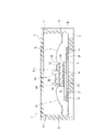
- FIG. 1 is a cross-sectional view showing a schematic configuration of an OCXO according to an embodiment to which the present invention is applied.
- FIG. 2 is a cross-sectional view showing a schematic configuration of a core portion and a core substrate of the OCXO of FIG.
- FIG. 3 is a plan view showing the core portion and the core substrate of FIG.
- FIG. 4 is a schematic configuration diagram schematically showing each configuration of the crystal oscillator (crystal oscillator and oscillation IC) of the core portion of FIG. 2.
- FIG. 5 is a schematic plan view of the first sealing member of the crystal oscillator of FIG. 4 on the first main surface side.
- FIG. 6 is a schematic plan view of the first sealing member of the crystal oscillator of FIG. 4 on the second main surface side.
- FIG. 7 is a schematic plan view of the crystal diaphragm of the crystal oscillator of FIG. 4 on the first main surface side.
- FIG. 8 is a schematic plan view of the crystal diaphragm of the crystal oscillator of FIG. 4 on the second main surface side.
- FIG. 9 is a schematic plan view of the second sealing member of the crystal oscillator of FIG. 4 on the first main surface side.
- FIG. 10 is a schematic plan view of the second sealing member of the crystal oscillator of FIG. 4 on the second main surface side.
- FIG. 11 is a cross-sectional view showing a schematic configuration of the OCXO according to the modified example 1.
- FIG. 12 is a plan view of the OCXO of FIG.
- FIG. 13 is a cross-sectional view showing a schematic configuration of the OCXO according to the modified example 2.
- FIG. 14 is a cross-sectional view showing a schematic configuration of the OCXO according to the modified example 3.
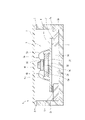
- the OCXO 1 has a structure in which a core portion 5 is arranged inside a substantially rectangular cuboid package (housing) 2 made of ceramic or the like, and is airtightly sealed by a lid (lid) 3. It is said that.
- the package 2 is formed with a recess 2a having an opening at the upper side, and the core portion 5 is sealed inside the recess 2a in an airtight state.
- a lid 3 is fixed to the upper surface of the peripheral wall portion 2b surrounding the recess 2a by seam welding via a sealing material 8, and the inside of the package 2 is in a sealed state (airtight state).
- the sealing material 8 for example, an Au-Su alloy or a metal-based sealing material such as solder is preferably used, but a sealing material such as low melting point glass may be used.
- the internal space of the package 2 is preferably a vacuum or an atmosphere having a low thermal conductivity such as low-pressure nitrogen or argon.
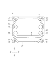
- a stepped portion 2c along the line of connection terminals (not shown) is formed on the inner wall surface of the peripheral wall portion 2b of the package 2, and the connection terminals formed on the stepped portion 2c are connected via a plate-shaped core substrate 4.
- the core portion 5 is connected to the core portion 5.
- the core substrate 4 is arranged so as to be bridged between the pair of stepped portions 2c and 2c of the package 2 facing each other, and is located between the pair of stepped portions 2c and 2c and on the lower portion of the core substrate 4. In, the space 2d is formed. Then, the connection terminal formed on the step surface of the step portion 2c is connected to the connection terminal (not shown) formed on the lower surface 4b of the core substrate 4 via the conductive adhesive 7.
- each component of the core portion 5 is connected to the connection terminals 4c formed on the upper surface 4a of the core substrate 4 via wires 6a and 6b by wire bonding.
- the conductive adhesive 7 for example, a polyimide adhesive, an epoxy adhesive, or the like is used.
- the core portion 5 is a package of various electronic components used in the OCXO1 and has a three-layer structure (laminated structure) in which an oscillation IC 51, a crystal oscillator 50, and a heater IC 52 are laminated in order from the upper side. It has become.
- the crystal oscillator 50 one having a three-layer structure in which the vibrating portion 11 is hermetically sealed is used. The areas of the oscillation IC 51, the crystal oscillator 50, and the heater IC 52 are gradually reduced in plan view.
- the core portion 5 is configured to stabilize the oscillation frequency of the OCXO1 by adjusting the temperature of the crystal oscillator 50, the oscillation IC 51, and the heater IC 52. Although the various electronic components of the core portion 5 are not sealed with the sealing resin, they may be sealed with the sealing resin depending on the sealing atmosphere.
- the crystal oscillator 100 is configured by the crystal oscillator 50 and the oscillation IC 51.
- the oscillation IC 51 is mounted on the crystal oscillator 50 via a plurality of metal bumps 51a (see FIG. 4).
- the oscillation frequency of OCXO1 is controlled by controlling the piezoelectric vibration of the crystal oscillator 50 by the oscillation IC 51. The details of the crystal oscillator 100 will be described later.
- a non-conductive adhesive (underfill) 53 is interposed between the facing surfaces of the crystal oscillator 50 and the oscillation IC 51, and the non-conductive adhesive 53 causes the crystal oscillator 50 and the oscillation IC 51 to have a non-conductive adhesive 53.
- the facing surfaces of each other are fixed.
- the upper surface of the crystal oscillator 50 (the first main surface 201 of the first sealing member 20) and the lower surface of the oscillation IC 51 are joined via the non-conductive adhesive 53.
- the non-conductive adhesive 53 for example, a polyimide adhesive, an epoxy adhesive, or the like is used.
- the external terminal (electrode pattern 22 shown in FIG. 5) formed on the upper surface of the crystal oscillator 50 is connected to the connection terminal 4c formed on the upper surface 4a of the core substrate 4 via the wire 6a by wire bonding. There is.
- the area of the oscillation IC 51 is smaller than that of the crystal oscillator 50 in a plan view, and the entire oscillation IC 51 is located within the range of the crystal oscillator 50 in a plan view.
- the entire lower surface of the oscillation IC 51 is joined to the upper surface of the crystal oscillator 50 (first main surface 201 of the first sealing member 20).
- the heater IC 52 has, for example, a configuration in which a heating element (heat source), a control circuit for controlling the temperature of the heating element (circuit for current control), and a temperature sensor for detecting the temperature of the heating element are integrated. Has been done. By controlling the temperature of the core portion 5 by the heater IC 52, the temperature of the core portion 5 is maintained at a substantially constant temperature, and the oscillation frequency of the OCXO1 is stabilized.
- a non-conductive adhesive 54 is interposed between the facing surfaces of the crystal oscillator 50 and the heater IC 52, and the non-conductive adhesive 54 causes the crystal oscillator 50 and the heater IC 52 to face each other. Is fixed. In this case, the lower surface of the crystal oscillator 50 (the second main surface 302 of the second sealing member 30) and the upper surface of the heater IC 52 are joined via the non-conductive adhesive 54.
- the non-conductive adhesive 54 for example, a polyimide-based adhesive, an epoxy-based adhesive, or the like is used.
- An external terminal (not shown) formed on the upper surface of the heater IC 52 is connected to the connection terminal 4c formed on the upper surface 4a of the core substrate 4 via wire 6b by wire bonding.
- the area of the crystal oscillator 50 in a plan view is smaller than that of the heater IC 52, and the entire crystal oscillator 50 is located within the range of the heater IC 52 in a plan view.
- the entire lower surface of the crystal oscillator 50 (second main surface 302 of the second sealing member 30) is joined to the upper surface of the heater IC 52.
- a conductive adhesive 55 is interposed between the facing surfaces of the heater IC 52 and the core substrate 4, and the facing surfaces of the heater IC 52 and the core substrate 4 are fixed by the conductive adhesive 55. There is. In this case, the lower surface of the heater IC 52 and the upper surface 4a of the core substrate 4 are joined via the conductive adhesive 55. As a result, the heater IC 52 is ground-connected via the conductive adhesive 55 and the core substrate 4.
- the conductive adhesive 55 for example, a polyimide adhesive, an epoxy adhesive, or the like is used.
- a non-conductive adhesive similar to the above-mentioned non-conductive adhesives 53 and 54 may be used instead of the conductive adhesive. good.
- connection terminals 4c are formed on the upper surface 4a of the core substrate 4.
- a plurality of (two in FIG. 3) chip capacitors (bypass capacitors) 4d are arranged on the upper surface 4a of the core substrate 4.
- the size and number of the chip capacitors 4d are not particularly limited.
- the type of the crystal oscillator 50 used for the core portion 5 is not particularly limited, but a device having a sandwich structure, which makes it easy to make the device thinner, can be preferably used.
- the device having a sandwich structure is composed of first and second sealing members made of glass or crystal, and a piezoelectric diaphragm made of crystal and having a vibrating portion having excitation electrodes formed on both main surfaces, for example. It is a device with a three-layer structure in which a stop member and a second sealing member are laminated and joined via a piezoelectric diaphragm, and the vibrating portion of the piezoelectric diaphragm arranged inside is airtightly sealed.
- the crystal oscillator 100 in which the crystal oscillator 50 having such a sandwich structure and the oscillation IC 51 are integrally provided will be described with reference to FIGS. 4 to 10.
- the crystal oscillator 100 includes a crystal diaphragm (piezoelectric diaphragm) 10, a first sealing member 20, a second sealing member 30, and an oscillation IC 51.
- the crystal diaphragm 10 and the first sealing member 20 are joined, and the crystal diaphragm 10 and the second sealing member 30 are joined to form a package having a substantially rectangular sandwich structure. Will be done. That is, in the crystal oscillator 100, the internal space (cavity) of the package is formed by joining the first sealing member 20 and the second sealing member 30 to both main surfaces of the crystal diaphragm 10.
- the vibrating portion 11 (see FIGS. 7 and 8) is hermetically sealed in the internal space.
- the crystal oscillator 100 has a package size of, for example, 1.0 ⁇ 0.8 mm, and is designed to be compact and have a low profile. Further, with the miniaturization, in the package, the electrodes are made conductive by using through holes without forming castings.
- the oscillation IC 51 mounted on the first sealing member 20 is a one-chip integrated circuit element that constitutes an oscillation circuit together with the crystal diaphragm 10. Further, the crystal oscillator 100 is mounted on the heater IC 52 described above via the non-conductive adhesive 54.
- the crystal diaphragm 10 is a piezoelectric substrate made of quartz, and both main surfaces (first main surface 101 and second main surface 102) are flat and smooth surfaces (mirror surface processing). Is formed as.
- the crystal diaphragm 10 an AT-cut quartz plate that performs thickness sliding vibration is used.
- both main surfaces 101 and 102 of the crystal diaphragm 10 are formed as XZ'planes.
- the direction parallel to the lateral direction (short side direction) of the crystal vibrating plate 10 is the X-axis direction
- the direction parallel to the longitudinal direction (long side direction) of the crystal vibrating plate 10 is the Z'axis. It is said to be the direction.
- a pair of excitation electrodes (first excitation electrode 111, second excitation electrode 112) are formed on both main surfaces 101 and 102 of the crystal diaphragm 10.
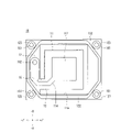
- the crystal diaphragm 10 holds the vibrating portion 11 by connecting the vibrating portion 11 formed in a substantially rectangular shape, the outer frame portion 12 surrounding the outer circumference of the vibrating portion 11, and the vibrating portion 11 and the outer frame portion 12. It has a holding portion (connecting portion) 13 and a holding portion (connecting portion) 13. That is, the crystal diaphragm 10 has a configuration in which the vibrating portion 11, the outer frame portion 12, and the holding portion 13 are integrally provided.
- the holding portion 13 extends (projects) from only one corner portion of the vibrating portion 11 located in the + X direction and the ⁇ Z ′ direction to the outer frame portion 12 in the ⁇ Z ′ direction.
- a penetration portion (slit) 11a is formed between the vibrating portion 11 and the outer frame portion 12, and the vibrating portion 11 and the outer frame portion 12 are connected by only one holding portion 13.
- the first excitation electrode 111 is provided on the first main surface 101 side of the vibrating portion 11, and the second excitation electrode 112 is provided on the second main surface 102 side of the vibrating portion 11.
- Extract wiring (first extraction wiring 113, second extraction wiring 114) for connecting these excitation electrodes to the external electrode terminals is connected to the first excitation electrode 111 and the second excitation electrode 112.
- the first lead-out wiring 113 is drawn out from the first excitation electrode 111 and is connected to the connection joint pattern 14 formed in the outer frame portion 12 via the holding portion 13.
- the second lead-out wiring 114 is drawn out from the second excitation electrode 112 and is connected to the connection joint pattern 15 formed on the outer frame portion 12 via the holding portion 13.
- the vibration side first joining pattern 121 is formed as the vibration side sealing portion of the first main surface 101
- the vibration side second joining pattern 122 is formed as the vibration side sealing portion of the second main surface 102.
- the vibration-side first joint pattern 121 and the vibration-side second joint pattern 122 are provided on the outer frame portion 12, and are formed in an annular shape in a plan view.
- the crystal diaphragm 10 is formed with five through holes penetrating between the first main surface 101 and the second main surface 102.
- the four first through holes 161 are provided in the regions of the four corners (corners) of the outer frame portion 12, respectively.
- the second through hole 162 is an outer frame portion 12, and is provided on one side of the vibrating portion 11 in the Z'axis direction (on the ⁇ Z'direction side in FIGS. 7 and 8).
- a connection pattern 123 is formed around the first through hole 161.
- a connection joint pattern 124 is formed on the first main surface 101 side, and a connection joint pattern 15 is formed on the second main surface 102 side.
- first through hole 161 and the second through hole 162 through electrodes for conducting the electrodes formed on the first main surface 101 and the second main surface 102 are provided along the inner wall surface of each of the through holes. It is formed. Further, the central portion of each of the first through hole 161 and the second through hole 162 is a hollow through portion penetrating between the first main surface 101 and the second main surface 102.
- the first sealing member 20 is a rectangular cuboid substrate formed from one AT-cut quartz plate, and the second main surface of the first sealing member 20.
- the 202 (the surface joined to the crystal diaphragm 10) is formed as a flat smooth surface (mirror surface processing).
- the coefficient of thermal expansion of the crystal vibrating plate 10 and the first sealing member 20 can be determined by using the AT-cut crystal plate as in the crystal vibrating plate 10. It can be the same, and thermal deformation in the crystal oscillator 100 can be suppressed. Further, the directions of the X-axis, the Y-axis, and the Z'axis of the first sealing member 20 are also the same as those of the quartz diaphragm 10.
- six electrode patterns 22 including a mounting pad for mounting an oscillation IC 51, which is an oscillation circuit element, are formed on the first main surface 201 of the first sealing member 20.
- the oscillation IC 51 is bonded to the electrode pattern 22 by a FCB (Flip Chip Bonding) method using a metal bump (for example, Au bump or the like) 51a (see FIG. 4).
- the electrode patterns 22 located at the four corners (corners) of the first main surface 201 of the first sealing member 20 are the upper surface 4a of the core substrate 4 described above. It is connected to the connection terminal 4c formed in the above via a wire 6a.
- the oscillation IC 51 is electrically connected to the outside via the wire 6a, the core substrate 4, the package 2, and the like.
- the first sealing member 20 is connected to each of the six electrode patterns 22 and has six throughs penetrating between the first main surface 201 and the second main surface 202.
- a hole is formed.
- four third through holes 211 are provided in the regions of the four corners (corners) of the first sealing member 20.
- the fourth and fifth through holes 212 and 213 are provided in the + Z'direction and the ⁇ Z'direction in FIGS. 5 and 6, respectively.
- each of the through holes 211 and the fourth and fifth through holes 212 and 213 through electrodes for conducting the electrodes formed on the first main surface 201 and the second main surface 202 are provided in each of the through holes. It is formed along the inner wall surface. Further, the central portion of each of the third through hole 211 and the fourth and fifth through holes 212 and 213 is a hollow through portion penetrating between the first main surface 201 and the second main surface 202.
- a sealing-side first joining pattern 24 is formed as a sealing-side first sealing portion for joining to the quartz diaphragm 10.
- the first bonding pattern 24 on the sealing side is formed in an annular shape in a plan view.
- connection pattern 25 is formed around the third through hole 211, respectively.
- a connection pattern 261 is formed around the fourth through hole 212, and a connection joint pattern 262 is formed around the fifth through hole 213.
- a connection joint pattern 263 is formed on the opposite side (-Z'direction side) of the first sealing member 20 in the major axis direction with respect to the connection joint pattern 261, and is connected to the connection joint pattern 261. It is connected to the joint pattern 263 by a wiring pattern 27.
- the second sealing member 30 is a rectangular cuboid substrate formed from one AT-cut quartz plate, and the first main surface of the second sealing member 30.
- the 301 (the surface joined to the crystal diaphragm 10) is formed as a flat smooth surface (mirror surface processing). It is desirable that the second sealing member 30 also uses an AT-cut quartz plate as in the quartz diaphragm 10, and the directions of the X-axis, the Y-axis, and the Z'axis are the same as those of the quartz diaphragm 10.
- a sealing-side second joining pattern 31 is formed as a sealing-side second sealing portion for joining to the quartz diaphragm 10.
- the second bonding pattern 31 on the sealing side is formed in an annular shape in a plan view.
- Electrode terminals 32 are provided on the second main surface 302 of the second sealing member 30.
- the electrode terminals 32 are located at the four corners (corners) of the second main surface 302 of the second sealing member 30.
- the electrical connection with the outside is made via the electrode pattern 22 and the wire 6a, but the electrical connection with the outside can also be made by using the electrode terminal 32. It is possible.
- the second sealing member 30 is formed with four through holes penetrating between the first main surface 301 and the second main surface 302.
- the four sixth through holes 33 are provided in the regions of the four corners (corners) of the second sealing member 30.
- through electrodes for conducting conduction of the electrodes formed on the first main surface 301 and the second main surface 302 are formed along the inner wall surface of each of the sixth through holes 33. There is. Through the through electrodes formed on the inner wall surface of the sixth through hole 33 in this way, the electrodes formed on the first main surface 301 and the electrode terminals 32 formed on the second main surface 302 are conductive.
- each of the sixth through holes 33 is a hollow through portion penetrating between the first main surface 301 and the second main surface 302. Further, on the first main surface 301 of the second sealing member 30, a connection pattern 34 is formed around the sixth through hole 33, respectively.
- the electrode terminal 32 is not used for electrical connection with the outside, the electrode terminal 32, the sixth through hole 33, and the like may not be provided.
- the crystal diaphragm 10 and the first sealing member 20 are sealed with the vibration side first joining pattern 121.
- the first bonding pattern 24 on the stop side was overlapped and diffusion-bonded, and the crystal diaphragm 10 and the second sealing member 30 overlapped the second bonding pattern 122 on the vibration side and the second bonding pattern 31 on the sealing side.
- connection joining patterns are also diffusely joined in a superposed state.
- the crystal oscillator 100 can obtain electrical conduction between the first excitation electrode 111, the second excitation electrode 112, the oscillation IC 51, and the electrode terminal 32.
- the first excitation electrode 111 is connected to the oscillation IC 51 via the first lead wiring 113, the wiring pattern 27, the fourth through hole 212, and the electrode pattern 22 in this order.
- the second excitation electrode 112 is connected to the oscillation IC 51 via the second lead-out wiring 114, the second through hole 162, the fifth through hole 213, and the electrode pattern 22 in this order.
- the various junction patterns are such that a plurality of layers are laminated on a quartz plate, and a Ti (titanium) layer and an Au (gold) layer are vapor-deposited from the lowest layer side thereof. Is preferable. Further, if the other wirings and electrodes formed on the crystal oscillator 100 have the same configuration as the joining pattern, the joining pattern, wirings and electrodes can be patterned at the same time, which is preferable.
- the sealing portions (seal paths) 115 and 116 that airtightly seal the vibrating portion 11 of the crystal diaphragm 10 are formed in an annular shape in a plan view.
- the seal path 115 is formed by diffusion bonding of the vibration-side first bonding pattern 121 and the sealing-side first bonding pattern 24 described above, and the outer edge shape and the inner edge shape of the seal path 115 are formed in a substantially octagonal shape.
- the seal path 116 is formed by the diffusion bonding of the vibration side second bonding pattern 122 and the sealing side second bonding pattern 31 described above, and the outer edge shape and the inner edge shape of the seal path 116 are formed in a substantially octagonal shape.
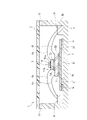
- the core portion 5 includes a crystal oscillator 50 having a three-layer structure in which the vibrating portion 11 is airtightly sealed, and an IC 52 for a heater as a heating element. At least one entire main surface of the crystal oscillator 50 is thermally coupled to the heater IC 52. In this case, the entire second main surface 302 of the second sealing member 30 of the crystal oscillator 50 is in surface contact with the upper surface of the heater IC 52 via the non-conductive adhesive 54 (second adhesive). There is.
- the entire second main surface 302 of the second sealing member 30 of the three-layered crystal oscillator 50 is thermally coupled to the heater IC 52, so that the crystal oscillator 50 is made more efficient. Can be heated. As a result, the temperature of the core portion 5 can be raised to a target temperature more quickly, and fluctuations in the frequency of OCXO1 can be suppressed.
- an oscillation IC 51 is mounted on the crystal oscillator 50, and the entire active surface (lower surface in FIGS. 1 and 4) of the oscillation IC 51 is thermally coupled to the crystal oscillator 50. .. In this case, the entire active surface of the oscillation IC 51 is in surface contact with the first main surface 301 of the first sealing member 20 of the crystal oscillator 50 via the non-conductive adhesive 53. As a result, the core portion 5 including the oscillation IC 51, the crystal oscillator 50, and the heater IC 52 can be heated to a target temperature faster.
- the heat capacity of the crystal oscillator 50 is smaller than the heat capacity of the heater IC 52.
- the temperature of the crystal oscillator 50 having a three-layer structure can be rapidly raised, and fluctuations in the frequency of OCXO1 can be suppressed.
- the heat capacity of the oscillating IC 51 is also smaller than the heat capacity of the heater IC 52, and the core portion 5 including the oscillating IC 51, the crystal oscillator 50, and the heater IC 52 is heated to a target temperature faster. Can be done.
- the heat capacity increases in the order of the oscillation IC 51, the crystal oscillator 50, and the heater IC 52.
- the thickness also increases in the order of the oscillation IC 51, the crystal oscillator 50, and the heater IC 52.
- the thickness of the oscillation IC 51 is 0.08 to 0.10 mm
- the thickness of the crystal oscillator 50 is 0.12 mm
- the thickness of the heater IC 52 is 0.28 to 0.30 mm.
- the oscillation IC 51, the crystal oscillator 50, and the heater IC 52 are laminated in order from the upper side in a three-layer structure (laminated structure), but the heater IC 52 which is a heating element is used. It has the largest heat capacity. As a result, the core portion 5 including the oscillation IC 51, the crystal oscillator 50, and the heater IC 52 can be heated to a target temperature faster.
- the junction region between the crystal oscillator 50 and the heater IC 52 is contained within the region on the upper surface of the heater IC 52, so that heat conduction from the heater IC 52 to the crystal oscillator 50 is efficient. This can be done, and the temperature of the crystal oscillator 50 can be raised quickly.
- the core portion 5 is mounted inside the package 2 made of an insulating material, and the lid 3 is joined to the package 2 to be airtightly sealed.
- the package 2 is made of a ceramic such as alumina.
- the core portion 5 is not exposed to the external environment, so that the temperature of the core portion 5 is increased. Can be made constant temperature.
- the stress from the mounting substrate on which the OCXO 1 is mounted is less likely to be transmitted to the core portion 5, and the core portion 5 can be protected. ..
- the core portion 5 includes a core substrate 4 bonded to the heater IC 52 via a bonding material, and the core substrate 4 is an insulating material having a lower thermal conductivity than the package 2. Is formed by.
- the core substrate 4 is made of quartz, glass, or resin.
- the core portion 5 includes the core substrate 4 made of an insulating material having a lower thermal conductivity than the package 2, so that the heat of the crystal oscillator 50 heated by the heater IC 52 can be transferred to, for example, alumina. It is possible to suppress conduction to the package 2 side using a suitable ceramic as a base material.
- the core substrate 4 it is preferable to use a resin substrate having a heat resistance of 200 ° C. or higher. Examples of the material of such a resin substrate include polyimide, glass epoxy, epoxy, and super engineering plastic. Further, it is preferable that no wiring is formed on the surface of the core substrate 4.
- the core substrate 4 is bonded to the package 2 via the conductive adhesive 7 (first adhesive).
- first adhesive the thermal conductivity of the non-conductive adhesive 54 (second adhesive) interposed between the facing surfaces of the crystal transducer 50 and the heater IC 52 is such that the core substrate 4 and the package 2 face each other. It is higher than the thermal conductivity of the conductive adhesive 7 (first adhesive) interposed between the surfaces.
- the thermal conductivity of the non-conductive adhesive 54 is higher than the thermal conductivity of the conductive adhesive 7
- the heat from the heater IC 52 is transferred to the crystal oscillator 50 before the package 2 side. And it can be efficiently conducted to the oscillating IC 51 on the crystal oscillator 50.
- the thermal conductivity of the non-conductive adhesive 54 interposed between the facing surfaces of the crystal transducer 50 and the heater IC 52 is the conductivity interposed between the facing surfaces of the heater IC 52 and the core substrate 4. It is preferable that the thermal conductivity is higher than that of the sex adhesive 55, or that the thermal conductivity of the non-conductive adhesive 54 and the thermal conductivity of the conductive adhesive 55 are substantially the same.
- the crystal oscillator 50 having a three-layer structure in which the vibrating portion 11 is hermetically sealed inside and the height can be reduced is used.
- the height of the core portion 5 can be reduced and the size can be reduced, and the heat capacity of the core portion 5 can be reduced.
- the thickness of the crystal oscillator 50 is, for example, 0.12 mm, which is much thinner than that of the conventional crystal oscillator.
- the heat capacity of the core portion 5 can be made very small as compared with the conventional OCXO, and the amount of heat generated by the heater of the OCXO1 provided with such a core portion 5 can be suppressed, which contributes to low power consumption. can do.
- the temperature followability of the core portion 5 can be improved, and the stability of the OCXO1 can be improved.
- the vibrating portion 11 is hermetically sealed without using an adhesive, so that the adverse effect of heat convection due to the outgas generated from the adhesive can be suppressed. Can be done. That is, heat convection may be generated by the circulation of the outgas generated from the adhesive in the space for airtightly sealing the vibrating portion 11, and the accurate temperature control of the vibrating portion 11 may be hindered.
- such outgas is not generated, so that the temperature of the vibrating portion 11 can be controlled with high accuracy.
- the sealing material formed by joining the seal paths 115 and 116 and the joining patterns for connection described above is composed of a thin film metal layer, so that the crystal oscillator 50 has a structure.
- the heat conduction in the vertical direction (stacking direction) is improved, and the temperature of the crystal oscillator 50 can be quickly made uniform.
- the thickness of the thin film metal layer is 1.00 ⁇ m or less (specifically, in the Au-Au junction of the present embodiment, 0.15 ⁇ m to 1.00 ⁇ m), and Sn is set. It is much thinner than the conventional metal paste encapsulant used (eg, 5 ⁇ m to 20 ⁇ m).
- a penetrating portion 11a is formed between the vibrating portion 11 and the outer frame portion 12 of the crystal diaphragm 10, and the vibrating portion 11 and the outer frame portion 12 have only one holding portion 13. Connected by.
- the holding portion 13 extends from only one corner portion of the vibrating portion 11 located in the + X direction and the ⁇ Z ′ direction to the outer frame portion 12 in the ⁇ Z ′ direction.
- the holding portion 13 is provided at a portion other than the corner portion (center portion of the side).
- the piezoelectric vibration It is possible to suppress the leakage of the piezoelectric vibration to the outer frame portion 12 via the holding portion 13, and it is possible to vibrate the vibrating portion 11 more efficiently. Further, as compared with the case where two or more holding portions 13 are provided, the stress acting on the vibrating portion 11 can be reduced, and the frequency shift of the piezoelectric vibration caused by such stress is reduced to stabilize the piezoelectric vibration. It is possible to improve the sex.
- the electrode terminal 32 formed on the bottom surface of the crystal oscillator 50 (the second main surface 302 of the second sealing member 30) is formed on the upper surface of the crystal oscillator 50 (the first main surface 201 of the first sealing member 20). ) Is electrically connected to the electrode pattern 22 formed in.
- the heat from the heater IC 52 can be conducted to the upper surface side of the crystal oscillator 50 via the electrode terminal 32 on the bottom surface side of the crystal oscillator 50, and the temperature of the crystal oscillator 50 is rapidly raised. be able to.
- the structure of the crystal oscillator 50 having a three-layer structure described above is an example, and can be changed in various ways.
- the vibrating portion 11 of the crystal diaphragm 10 may have an inverted mesa structure formed to be thinner than the outer frame portion 12.
- the first sealing member 20 and the second sealing member 30 are not limited to a flat plate shape, and may have a shape having a thickened side wall on the outer peripheral portion.
- Package 2 The structure of Package 2 described above is an example and can be changed in various ways.
- a package having an H-shaped cross section may be used.
- the oscillation IC 51 is mounted on the crystal oscillator 50 by the FCB method using a metal bump, but the present invention is not limited to this, and the crystal vibration of the oscillation IC 51 is performed by wire bonding, a conductive adhesive, or the like. It may be mounted on the child 50.
- the heater IC 52 was mounted on the core substrate 4 by wire bonding, but the present invention is not limited to this, and the heater IC 52 is mounted on the core substrate 4 by the FCB method using metal bumps or a conductive adhesive. May be done.
- the crystal oscillator 50 is electrically connected to the core substrate 4 by wire bonding, but the present invention is not limited to this, and the crystal oscillator 50 is used for a heater by the FCB method using a metal bump, a conductive adhesive, or the like. By mounting the crystal oscillator 50 on the IC 52, the crystal oscillator 50 may be electrically connected to the core substrate 4 via the heater IC 52.
- the core portion 5 has a configuration in which the oscillation IC 51, the crystal oscillator 50, and the heater IC 52 are stacked in order from the upper side, but conversely, the core portion 5 is the heater IC 52.
- the crystal oscillator 50, and the oscillation IC 51 may be stacked in order from the upper side.
- a heater substrate or the like may be added to the laminated structure of the oscillation IC 51, the crystal oscillator 50, and the heater IC 52 of the core portion 5 described above.
- the heater substrate, the oscillation IC 51, the crystal oscillator 50, and the heater IC 52 may be stacked in order from the upper side in a four-layer structure, or the heater IC 52, the crystal oscillator 50, the oscillation IC 51, and the heater substrate may be formed.
- it may be a four-layer structure in which the layers are stacked in order from the upper side. In these cases, the temperature of the core portion 5 can be made more uniform by laminating a heater substrate which is a heating element on the oscillation IC 51.
- the core portion 5 has a three-layer structure in which the oscillation IC 51, the crystal oscillator 50, and the heater IC 52 are laminated, but the core portion 5 is not limited to this, and the core portion 5 is the heater IC 52.
- the crystal oscillator 50 and the oscillation IC 51 may be mounted on the surface in a horizontal position (see, for example, FIG. 14).
- the entire second main surface 302 of the second sealing member 30 of the crystal oscillator 50 is in surface contact with the upper surface of the heater IC 52 via a non-conductive adhesive.
- the entire active surface of the oscillation IC 51 may be surface-contacted with the upper surface of the heater IC 52 via a non-conductive adhesive.
- the crystal oscillator 50 and the oscillation IC 51 may be electrically connected by a wire.
- the entire second main surface 302 of the second sealing member 30 of the crystal oscillator 50 is thermally coupled to the heater IC 52, but the other main surface of the crystal oscillator 50 (first seal).
- the entire first main surface 201) of the stop member 20 may also be thermally coupled to another heating element (for example, a heater substrate).
- a heater substrate for example, a heater substrate in which a metal film meanderingly formed on the surface of a quartz substrate can be used.
- the crystal diaphragm 10 and the first and second sealing members 20 and 30 of the crystal oscillator 50 are AT-cut crystal plates, but an SC-cut crystal plate is used instead of the AT-cut crystal plate. You may.
- the conduction of the electrodes in the crystal oscillator 50 is performed through the through hole, but the conduction is performed through the inner wall surface of the package of the crystal oscillator 50, the wall surface of the outer wall surface, and the casting provided on the side wall. Conduction of the electrodes may be performed. In this case, it is effective when the package of the crystal oscillator 50 is miniaturized.
- FIG. 11 is a cross-sectional view showing a schematic configuration of OCXO1 according to the modified example 1.
- FIG. 12 is a plan view of OCXO1 of FIG.
- FIG. 13 is a cross-sectional view showing a schematic configuration of OCXO1 according to Modification 2.
- FIG. 14 is a cross-sectional view showing a schematic configuration of OCXO1 according to the modified example 3.
- the OCXO 1 according to the first modification is made of ceramic or the like, and the core portion 5 is arranged inside the package (housing) 2 having a substantially rectangular cuboid, and is hermetically sealed by the lid (lid) 3. It is said to have a structure.
- Package 2 has a size of, for example, 5.0 ⁇ 3.2 mm.
- the package 2 is formed with a recess 2a having an opening at the upper side, and the core portion 5 is sealed inside the recess 2a in an airtight state.
- a lid 3 is fixed to the upper surface of the peripheral wall portion 2b surrounding the recess 2a by seam welding via a sealing material 8, and the inside of the package 2 is in a sealed state (airtight state).
- the sealing material 8 for example, an Au—Su alloy or a metal-based sealing material such as solder is preferably used, but a sealing material such as low melting point glass may be used. Further, not limited to these, it is also possible to adopt a structure of a sealing member by a method such as seam sealing using a metal ring, direct seam sealing using no metal ring, and beam sealing (vacuum degree). Seam sealing is preferable so as not to lower it).
- the internal space of the package 2 is preferably a vacuum (for example, a vacuum degree of 10 Pa or less) or an atmosphere having a low thermal conductivity such as low-pressure nitrogen or argon. Note that FIG. 12 shows OCXO1 with the lid 3 removed, and shows the internal structure of OCXO1.
- a stepped portion 2c along the line of connection terminals is formed on the inner wall surface of the peripheral wall portion 2b of the package 2.
- the core portion 5 is arranged on the bottom surface of the recess 2a (the inner bottom surface of the package 2) between the pair of stepped portions 2c and 2c facing each other via the plate-shaped core substrate 4.
- the step portion 2c may be formed so as to surround the four sides of the bottom surface of the recess 2a.
- the core substrate 4 is made of a heat-resistant and flexible resin material such as polyimide.
- the core substrate 4 may be formed of quartz.
- the core substrate 4 is joined to the bottom surface of the recess 2a (the inner bottom surface of the package 2) by the non-conductive adhesive 7a, and a space 2d is formed in the lower portion of the core substrate 4. Further, the external terminals formed on the respective constituent members of the core portion 5 are connected to the connection terminals formed on the stepped surface of the stepped portion 2c via the wires 6a and 6b by wire bonding. One end of the wire 6a is connected to an electrode pattern 22 (see FIG. 5) formed on the first main surface 201 of the first sealing member 20 of the crystal oscillator 50. One end of the wire 6b is connected to an external terminal (not shown) formed on the upper surface of the heater IC 52. Spacer members 2f and 2f are provided on the inner side of the non-conductive adhesives 7a and 7a.
- the non-conductive adhesives 7a and 7a are arranged at both ends in the longitudinal direction of the core substrate 4, and are arranged linearly along the lateral direction of the core substrate 4 (the direction orthogonal to the paper surface of FIG. 11). ing.
- Each spacer member 2f is arranged so as to be adjacent to the side of the non-conductive adhesive 7a, and is arranged linearly along the lateral direction of the core substrate 4.
- the spacer members 2f and 2f are interposed between the core substrate 4 and the inner bottom surface of the package 2 on the inner side of the non-conductive adhesives 7a and 7a. Both ends of the core substrate 4 in the longitudinal direction are supported by the spacer members 2f and 2f.
- the core substrate 4 is made of a heat-resistant and flexible resin material such as polyimide.
- the spacer member 2f is made of a paste material such as molybdenum or tungsten. In this way, inclusions of the non-conductive adhesive 7a and the spacer member 2f are provided between the core substrate 4 and the inner bottom surface of the package 2, and the inclusions provide the inner bottom surface of the core substrate 4 and the package 2.
- the space 2d between and the space 2d can be easily secured. Further, since the thickness of the non-conductive adhesive 7a applied to the inner bottom surface of the package 2 is defined by the spacer member 2f, the width (height dimension) of the space 2d between the core substrate 4 and the inner bottom surface of the package 2 is defined. ) Can be easily specified.
- the thickness of the spacer member 2f is preferably 5 to 50 ⁇ m.
- Underfill is not interposed between the facing surfaces of the crystal oscillator 50 and the oscillating IC 51, and the facing surfaces of the crystal oscillator 50 and the oscillating IC 51 are formed by a plurality of metal bumps 51a. It is fixed so that the influence of stress due to underfill can be avoided. It should be noted that an underfill may be interposed between the facing surfaces of the crystal oscillator 50 and the oscillation IC 51.
- the conductive adhesive 56 is interposed between the facing surfaces of the crystal oscillator 50 and the heater IC 52, but is non-conductive between the facing surfaces of the crystal oscillator 50 and the heater IC 52. It may be configured to intervene with a sex adhesive.
- the entire second main surface 302 of the second sealing member 30 of the crystal oscillator 50 is thermally coupled to the heater IC 52.
- the entire second main surface 302 of the second sealing member 30 of the crystal oscillator 50 is in surface contact with the upper surface of the heater IC 52 via the conductive adhesive 56 (second adhesive). ..
- the conductive adhesive 56 second adhesive
- at least the entire second main surface 302 of the second sealing member 30 of the three-layered crystal oscillator 50 is thermally coupled to the heater IC 52, so that the crystal oscillator 50 is made more efficient.
- the temperature of the core portion 5 can be raised to a target temperature more quickly, and fluctuations in the frequency of OCXO1 can be suppressed.
- the OCXO1 according to the modification 2 shown in FIG. 13 has substantially the same configuration as the OCXO1 according to the modification 1 shown in FIG. 11, but the crystal oscillator 50 and the oscillation IC 51 are electrically connected by wire bonding. The point is different from OCXO1 according to the modified example 1.
- the external terminals formed on each component of the core portion 5 are wire-bonded to the connection terminals formed on the stepped surface of the stepped portion 2c via the wires 6b and 6d. Is connected by.
- One end of the wire 6b is connected to an external terminal (not shown) formed on the upper surface of the heater IC 52.
- One end of the wire 6d is connected to an external terminal (not shown) formed on the active surface 51b of the oscillation IC 51.
- the active surface 51b of the oscillation IC 51 is arranged on the crystal oscillator 50 in an upward state.
- the crystal oscillator 50 and the oscillation IC 51 are electrically connected via the wire 6c.
- One end of the wire 6c is connected to an electrode pattern 22 (see FIG. 5) formed on the first main surface 201 of the first sealing member 20 of the crystal oscillator 50.
- the other end of the wire 6c is connected to an electrode pattern (not shown) formed on the active surface 51b of the oscillation IC 51.
- the oscillation IC 51 and the heater IC 52 are electrically connected via the wire 6e.
- One end of the wire 6e is connected to an external terminal (not shown) formed on the active surface 51b of the oscillation IC 51.
- the other end of the wire 6e is connected to an external terminal (not shown) formed on the upper surface of the heater IC 52.
- a non-conductive adhesive 58 is interposed between the facing surfaces of the crystal oscillator 50 and the oscillation IC 51, and the entire surface of the oscillation IC 51 opposite to the active surface 51b is the crystal oscillator 50.
- the first main surface 201 of the first sealing member 20 is in surface contact with the first main surface 201 via the non-conductive adhesive 58.
- a conductive adhesive may be interposed between the facing surfaces of the crystal oscillator 50 and the oscillation IC 51.
- the OCXO1 according to the modification 3 shown in FIG. 14 has substantially the same configuration as the OCXO1 according to the modifications 1 and 2 shown in FIGS. 11 and 13, but the crystal oscillator 50 and the crystal oscillator 50 are placed on the heater IC 52. It is different from OCXO1 according to Modifications 1 and 2 in that the oscillation IC 51 is mounted in a horizontal state instead of a stacked state.
- the external terminals formed on each component of the core portion 5 are connected to the connection terminals formed on the stepped surface of the stepped portion 2c via the wire 6b by wire bonding. Has been done.
- One end of the wire 6b is connected to an external terminal (not shown) formed on the upper surface of the heater IC 52.
- the crystal oscillator 50 and the oscillation IC 51 are electrically connected via the wire 6c.
- One end of the wire 6c is connected to an electrode pattern 22 (see FIG. 5) formed on the first main surface 201 of the first sealing member 20 of the crystal oscillator 50.
- the other end of the wire 6c is connected to an electrode pattern (not shown) formed on the active surface 51b of the oscillation IC 51.
- the crystal oscillator 50 and the heater IC 52 are electrically connected via the wire 6f.
- One end of the wire 6f is connected to an electrode pattern 22 (see FIG. 5) formed on the first main surface 201 of the first sealing member 20 of the crystal oscillator 50.
- the other end of the wire 6e is connected to an external terminal (not shown) formed on the upper surface of the heater IC 52.
- the active surface 51b of the oscillation IC 51 is arranged on the heater IC 52 in an upward state.
- a non-conductive adhesive 58 is interposed between the facing surfaces of the heater IC 52 and the oscillation IC 51, and the entire surface of the oscillation IC 51 opposite to the active surface 51b is not on the upper surface of the heater IC 52. It is in surface contact via the conductive adhesive 58.
- a conductive adhesive may be interposed between the facing surfaces of the heater IC 52 and the oscillation IC 51.
- the piezoelectric vibration device in which the core portion 5 is mounted inside the package 2 has been described.
- the core portion including the piezoelectric vibrator having a three-layer structure in which the vibration portion is airtightly sealed and the heating element is provided.
- the present invention can be applied to a piezoelectric vibration device in which the core portion is not housed inside the package, as long as it has at least the core portion.
- the piezoelectric vibration device in which the oscillation IC 51 is mounted on the crystal oscillator 50 has been described above, the present invention is also applied to the piezoelectric vibration device in which the oscillation IC is not mounted on the crystal oscillator 50. Applicable.
- the present invention can be used for a piezoelectric vibration device provided with a core portion including a piezoelectric vibrator having a three-layer structure in which a vibrating portion is airtightly sealed and a heating element.
Abstract
Description
2 パッケージ
4 コア基板
5 コア部
11 振動部
50 水晶振動子(圧電振動子)
52 ヒータ用IC(発熱体) 1 OCXO (Piezoelectric Vibration Device)
2
52 Heater IC (heating element)
Claims (8)
- 少なくともコア部を備えた圧電振動デバイスであって、
前記コア部には、振動部が気密封止された3枚重ね構造の圧電振動子と、発熱体が含まれ、
前記圧電振動子の少なくとも一主面全体が、前記発熱体と熱的に結合されていることを特徴とする圧電振動デバイス。 A piezoelectric vibration device with at least a core
The core portion includes a piezoelectric vibrator having a three-layer structure in which the vibrating portion is airtightly sealed, and a heating element.
A piezoelectric vibration device characterized in that at least one entire main surface of the piezoelectric vibrator is thermally coupled to the heating element. - 請求項1に記載の圧電振動デバイスにおいて、
前記圧電振動子上には、発振用ICが搭載されており、前記発振用ICの能動面全体が、前記圧電振動子または前記発熱体と熱的に結合されていることを特徴とする圧電振動デバイス。 In the piezoelectric vibration device according to claim 1,
An oscillation IC is mounted on the piezoelectric vibrator, and the entire active surface of the oscillation IC is thermally coupled to the piezoelectric vibrator or the heating element. device. - 請求項1または2に記載の圧電振動デバイスにおいて、
前記圧電振動子の熱容量が、前記発熱体の熱容量よりも小さいことを特徴とする圧電振動デバイス。 In the piezoelectric vibration device according to claim 1 or 2.
A piezoelectric vibration device characterized in that the heat capacity of the piezoelectric vibrator is smaller than the heat capacity of the heating element. - 請求項1~3のいずれか1つに記載の圧電振動デバイスにおいて、
前記コア部が、絶縁材料からなるパッケージの内部に実装されるとともに、前記パッケージに蓋が接合されることによって気密に封止されていることを特徴とする圧電振動デバイス。 The piezoelectric vibration device according to any one of claims 1 to 3.
A piezoelectric vibration device characterized in that the core portion is mounted inside a package made of an insulating material and is airtightly sealed by joining a lid to the package. - 請求項4に記載の圧電振動デバイスにおいて、
前記コア部には、前記発熱体に接合材を介して接合された基板が含まれており、
前記基板は、前記パッケージよりも熱伝導率が低い絶縁材料によって形成されていることを特徴とする圧電振動デバイス。 In the piezoelectric vibration device according to claim 4,
The core portion includes a substrate bonded to the heating element via a bonding material.
A piezoelectric vibration device characterized in that the substrate is formed of an insulating material having a lower thermal conductivity than the package. - 請求項5に記載の圧電振動デバイスにおいて、
前記絶縁材料は、水晶、ガラス、または樹脂であることを特徴とする圧電振動デバイス。 In the piezoelectric vibration device according to claim 5,
A piezoelectric vibration device, wherein the insulating material is quartz, glass, or resin. - 請求項6に記載の圧電振動デバイスにおいて、
前記基板が、第1の接着剤を介して前記パッケージに接合されていることを特徴とする圧電振動デバイス。 In the piezoelectric vibration device according to claim 6,
A piezoelectric vibration device, wherein the substrate is bonded to the package via a first adhesive. - 請求項7に記載の圧電振動デバイスにおいて、
前記圧電振動子と前記発熱体とが第2の接着剤を介して接合され、
前記第2の接着剤の熱伝導率が、前記第1の接着剤の熱伝導率よりも高いことを特徴とする圧電振動デバイス。 In the piezoelectric vibration device according to claim 7,
The piezoelectric vibrator and the heating element are bonded to each other via a second adhesive.
A piezoelectric vibration device characterized in that the thermal conductivity of the second adhesive is higher than the thermal conductivity of the first adhesive.
Priority Applications (2)
| Application Number | Priority Date | Filing Date | Title |
|---|---|---|---|
| CN202180088703.2A CN116671007A (en) | 2021-01-08 | 2021-12-28 | Piezoelectric vibration device |
| JP2022574035A JPWO2022149541A1 (en) | 2021-01-08 | 2021-12-28 |
Applications Claiming Priority (2)
| Application Number | Priority Date | Filing Date | Title |
|---|---|---|---|
| JP2021002000 | 2021-01-08 | ||
| JP2021-002000 | 2021-01-08 |
Publications (1)
| Publication Number | Publication Date |
|---|---|
| WO2022149541A1 true WO2022149541A1 (en) | 2022-07-14 |
Family
ID=82357971
Family Applications (1)
| Application Number | Title | Priority Date | Filing Date |
|---|---|---|---|
| PCT/JP2021/048747 WO2022149541A1 (en) | 2021-01-08 | 2021-12-28 | Piezoelectric oscillation device |
Country Status (4)
| Country | Link |
|---|---|
| JP (1) | JPWO2022149541A1 (en) |
| CN (1) | CN116671007A (en) |
| TW (1) | TWI821840B (en) |
| WO (1) | WO2022149541A1 (en) |
Citations (5)
| Publication number | Priority date | Publication date | Assignee | Title |
|---|---|---|---|---|
| JP2005165630A (en) * | 2003-12-02 | 2005-06-23 | Toyo Commun Equip Co Ltd | Temperature control circuit and homeothermal chamber type piezoelectric oscillator |
| JP2010283475A (en) * | 2009-06-02 | 2010-12-16 | Onkyo Corp | Piezoelectric oscillator |
| JP2015139053A (en) * | 2014-01-21 | 2015-07-30 | 株式会社大真空 | piezoelectric vibration device |
| JP2018014705A (en) * | 2016-07-07 | 2018-01-25 | 日本電波工業株式会社 | Thermostatic chamber type crystal oscillator |
| JP2018196105A (en) * | 2017-05-18 | 2018-12-06 | セイコーエプソン株式会社 | Oscillator and electronic apparatus |
Family Cites Families (1)
| Publication number | Priority date | Publication date | Assignee | Title |
|---|---|---|---|---|
| JP6390993B2 (en) * | 2015-12-25 | 2018-09-19 | 株式会社村田製作所 | Piezoelectric oscillator and piezoelectric oscillation device |
-
2021
- 2021-12-28 WO PCT/JP2021/048747 patent/WO2022149541A1/en active Application Filing
- 2021-12-28 TW TW110149129A patent/TWI821840B/en active
- 2021-12-28 CN CN202180088703.2A patent/CN116671007A/en active Pending
- 2021-12-28 JP JP2022574035A patent/JPWO2022149541A1/ja active Pending
Patent Citations (5)
| Publication number | Priority date | Publication date | Assignee | Title |
|---|---|---|---|---|
| JP2005165630A (en) * | 2003-12-02 | 2005-06-23 | Toyo Commun Equip Co Ltd | Temperature control circuit and homeothermal chamber type piezoelectric oscillator |
| JP2010283475A (en) * | 2009-06-02 | 2010-12-16 | Onkyo Corp | Piezoelectric oscillator |
| JP2015139053A (en) * | 2014-01-21 | 2015-07-30 | 株式会社大真空 | piezoelectric vibration device |
| JP2018014705A (en) * | 2016-07-07 | 2018-01-25 | 日本電波工業株式会社 | Thermostatic chamber type crystal oscillator |
| JP2018196105A (en) * | 2017-05-18 | 2018-12-06 | セイコーエプソン株式会社 | Oscillator and electronic apparatus |
Also Published As
| Publication number | Publication date |
|---|---|
| JPWO2022149541A1 (en) | 2022-07-14 |
| CN116671007A (en) | 2023-08-29 |
| TWI821840B (en) | 2023-11-11 |
| TW202245407A (en) | 2022-11-16 |
Similar Documents
| Publication | Publication Date | Title |
|---|---|---|
| WO2022025227A1 (en) | Thermostatic bath-type piezoelectric oscillator | |
| JPWO2020122179A1 (en) | Piezoelectric vibration device | |
| WO2022050414A1 (en) | Thermostatic bath-type piezoelectric oscillator | |
| WO2022149541A1 (en) | Piezoelectric oscillation device | |
| WO2021199790A1 (en) | Constant temperature bath-type piezoelectric oscillator | |
| TWI804210B (en) | Thermostatic Bath Type Piezoelectric Oscillator | |
| JP5468240B2 (en) | Temperature compensated crystal oscillator for surface mounting | |
| JP2013143607A (en) | Crystal oscillator for surface mounting | |
| JP2021158586A (en) | Piezoelectric oscillator | |
| WO2023182062A1 (en) | Thermostatic oven type piezoelectric oscillator | |
| JP2020104229A (en) | MEMS device | |
| TWI812028B (en) | Thermostatic Bath Type Piezoelectric Oscillator | |
| TW202245406A (en) | Thermostatic bath-type piezoelectric oscillator | |
| JP7435150B2 (en) | piezoelectric oscillator | |
| JP2021158644A (en) | Constant temperature bath type piezoelectric oscillator | |
| US20240136976A1 (en) | Oven-controlled crystal oscillator | |
| JP2022143325A (en) | Thermostatted Piezoelectric Oscillator | |
| JP2023051073A (en) | Thermostatted Piezoelectric Oscillator | |
| JP2022164190A (en) | vibration device | |
| JP2015106792A (en) | Crystal device | |
| JP2021141368A (en) | Piezoelectric device | |
| JP2021158463A (en) | Piezoelectric oscillator | |
| JP2010183331A (en) | Quartz oscillator for surface mounting |
Legal Events
| Date | Code | Title | Description |
|---|---|---|---|
| 121 | Ep: the epo has been informed by wipo that ep was designated in this application |
Ref document number: 21917761 Country of ref document: EP Kind code of ref document: A1 |
|
| ENP | Entry into the national phase |
Ref document number: 2022574035 Country of ref document: JP Kind code of ref document: A |
|
| WWE | Wipo information: entry into national phase |
Ref document number: 202180088703.2 Country of ref document: CN |
|
| NENP | Non-entry into the national phase |
Ref country code: DE |
|
| 122 | Ep: pct application non-entry in european phase |
Ref document number: 21917761 Country of ref document: EP Kind code of ref document: A1 |