WO2022149388A1 - 撮像装置および測距システム - Google Patents
撮像装置および測距システム Download PDFInfo
- Publication number
- WO2022149388A1 WO2022149388A1 PCT/JP2021/044739 JP2021044739W WO2022149388A1 WO 2022149388 A1 WO2022149388 A1 WO 2022149388A1 JP 2021044739 W JP2021044739 W JP 2021044739W WO 2022149388 A1 WO2022149388 A1 WO 2022149388A1
- Authority
- WO
- WIPO (PCT)
- Prior art keywords
- transistor
- signal
- switch
- state
- input terminal
- Prior art date
- Legal status (The legal status is an assumption and is not a legal conclusion. Google has not performed a legal analysis and makes no representation as to the accuracy of the status listed.)
- Ceased
Links
Images




Classifications
-
- H—ELECTRICITY
- H04—ELECTRIC COMMUNICATION TECHNIQUE
- H04N—PICTORIAL COMMUNICATION, e.g. TELEVISION
- H04N25/00—Circuitry of solid-state image sensors [SSIS]; Control thereof
- H04N25/70—SSIS architectures; Circuits associated therewith
- H04N25/76—Addressed sensors, e.g. MOS or CMOS sensors
- H04N25/78—Readout circuits for addressed sensors, e.g. output amplifiers or A/D converters
-
- H—ELECTRICITY
- H03—ELECTRONIC CIRCUITRY
- H03M—CODING; DECODING; CODE CONVERSION IN GENERAL
- H03M1/00—Analogue/digital conversion; Digital/analogue conversion
- H03M1/12—Analogue/digital converters
- H03M1/50—Analogue/digital converters with intermediate conversion to time interval
- H03M1/56—Input signal compared with linear ramp
-
- H—ELECTRICITY
- H04—ELECTRIC COMMUNICATION TECHNIQUE
- H04N—PICTORIAL COMMUNICATION, e.g. TELEVISION
- H04N23/00—Cameras or camera modules comprising electronic image sensors; Control thereof
- H04N23/56—Cameras or camera modules comprising electronic image sensors; Control thereof provided with illuminating means
-
- H—ELECTRICITY
- H04—ELECTRIC COMMUNICATION TECHNIQUE
- H04N—PICTORIAL COMMUNICATION, e.g. TELEVISION
- H04N23/00—Cameras or camera modules comprising electronic image sensors; Control thereof
- H04N23/60—Control of cameras or camera modules
- H04N23/667—Camera operation mode switching, e.g. between still and video, sport and normal or high- and low-resolution modes
-
- H—ELECTRICITY
- H04—ELECTRIC COMMUNICATION TECHNIQUE
- H04N—PICTORIAL COMMUNICATION, e.g. TELEVISION
- H04N25/00—Circuitry of solid-state image sensors [SSIS]; Control thereof
- H04N25/60—Noise processing, e.g. detecting, correcting, reducing or removing noise
- H04N25/62—Detection or reduction of noise due to excess charges produced by the exposure, e.g. smear, blooming, ghost image, crosstalk or leakage between pixels
- H04N25/627—Detection or reduction of inverted contrast or eclipsing effects
-
- H—ELECTRICITY
- H04—ELECTRIC COMMUNICATION TECHNIQUE
- H04N—PICTORIAL COMMUNICATION, e.g. TELEVISION
- H04N25/00—Circuitry of solid-state image sensors [SSIS]; Control thereof
- H04N25/70—SSIS architectures; Circuits associated therewith
- H04N25/703—SSIS architectures incorporating pixels for producing signals other than image signals
- H04N25/705—Pixels for depth measurement, e.g. RGBZ
-
- H—ELECTRICITY
- H04—ELECTRIC COMMUNICATION TECHNIQUE
- H04N—PICTORIAL COMMUNICATION, e.g. TELEVISION
- H04N25/00—Circuitry of solid-state image sensors [SSIS]; Control thereof
- H04N25/70—SSIS architectures; Circuits associated therewith
- H04N25/76—Addressed sensors, e.g. MOS or CMOS sensors
- H04N25/77—Pixel circuitry, e.g. memories, A/D converters, pixel amplifiers, shared circuits or shared components
- H04N25/772—Pixel circuitry, e.g. memories, A/D converters, pixel amplifiers, shared circuits or shared components comprising A/D, V/T, V/F, I/T or I/F converters
-
- H—ELECTRICITY
- H04—ELECTRIC COMMUNICATION TECHNIQUE
- H04N—PICTORIAL COMMUNICATION, e.g. TELEVISION
- H04N25/00—Circuitry of solid-state image sensors [SSIS]; Control thereof
- H04N25/70—SSIS architectures; Circuits associated therewith
- H04N25/76—Addressed sensors, e.g. MOS or CMOS sensors
- H04N25/779—Circuitry for scanning or addressing the pixel array
-
- H—ELECTRICITY
- H04—ELECTRIC COMMUNICATION TECHNIQUE
- H04N—PICTORIAL COMMUNICATION, e.g. TELEVISION
- H04N25/00—Circuitry of solid-state image sensors [SSIS]; Control thereof
- H04N25/70—SSIS architectures; Circuits associated therewith
- H04N25/76—Addressed sensors, e.g. MOS or CMOS sensors
- H04N25/7795—Circuitry for generating timing or clock signals
-
- H—ELECTRICITY
- H04—ELECTRIC COMMUNICATION TECHNIQUE
- H04N—PICTORIAL COMMUNICATION, e.g. TELEVISION
- H04N25/00—Circuitry of solid-state image sensors [SSIS]; Control thereof
- H04N25/70—SSIS architectures; Circuits associated therewith
- H04N25/76—Addressed sensors, e.g. MOS or CMOS sensors
- H04N25/767—Horizontal readout lines, multiplexers or registers
Definitions
- This disclosure relates to an imaging device and a ranging system.
- the signal line of the pixel signal is cut off during the boosting period of the FD, a voltage drop occurs in the comparator that processes the pixel signal. Due to this voltage decrease, the settling time may increase and the frame rate may decrease.
- the present disclosure provides an imaging device and a ranging system capable of suppressing a decrease in frame rate while improving charge transfer efficiency.
- the image pickup apparatus includes a photoelectric conversion element, a signal conversion unit that is boosted when the charge transferred from the photoelectric conversion element is converted into a pixel signal, and a pixel during the boost period of the signal conversion unit.
- a selection transistor that cuts off the signal line of the signal, a non-inverting input terminal to which a pixel signal is input via the selection transistor, an inverting input terminal to which a lamp signal is input, and a comparison result between the pixel signal and the lamp signal. It includes a comparator having an output terminal for output, and a correction circuit for holding the potential of the non-inverting input terminal during the boosting period at the potential of the non-inverting input terminal before the boosting period.
- the correction circuit A first transistor arranged between the selection transistor and the non-inverting input terminal, The first transistor, the pair of second transistors, and A first switch arranged between the gate of the first transistor and the gate of the second transistor, A second switch arranged between the source of the first transistor and the source of the second transistor, With a capacitor connected to the gate of the second transistor, During the boosting period, the first switch may be in the off state and the second switch may be in the on state.
- the threshold voltage between the gate and the source of the first transistor may be equal to the threshold voltage between the gate and the source of the second transistor.
- the first switch may be switched from the on state to the off state, and the second switch may be switched from the off state to the on state.
- the selection transistor switches from the on state to the off state, the first switch switches from the on state to the off state, and the second switch changes from the off state to the on state. You may switch.
- the first switch may be an N-channel MOSFET.
- the photoelectric conversion element, the signal conversion unit, and the selection transistor may be arranged on the first semiconductor substrate, and the comparator and the correction circuit may be arranged on the second semiconductor substrate laminated on the first semiconductor substrate.
- the photoelectric conversion element, the signal conversion unit, the selection transistor, the comparator, and the correction circuit may be arranged on one semiconductor substrate.
- a plurality of the photoelectric conversion elements are arranged two-dimensionally,
- the comparator and the correction circuit may be provided for each photoelectric conversion element.
- the image pickup device may be a global shutter system in which the plurality of photoelectric conversion elements accumulate the electric charge at the same timing.
- the image pickup device may be a rolling shutter system in which the plurality of photoelectric conversion elements accumulate the electric charges at different timings.
- the distance measuring system includes a lighting device that irradiates the distance measuring light and an image pickup device that receives the reflected light of the distance measuring light.
- the image pickup device has a photoelectric conversion element that photoelectrically converts the reflected light, a signal conversion unit that is boosted when the charge transferred from the photoelectric conversion element is converted into a pixel signal, and a pixel signal during the boost period of the signal conversion unit.
- a selection transistor that cuts off the signal line, a non-inverting input terminal to which a pixel signal is input via the selection transistor, an inverting input terminal to which a lamp signal is input, and an output that outputs a comparison result between the pixel signal and the lamp signal. It has a comparator having a terminal, and a correction circuit that holds the potential of the non-inverting input terminal during the boosting period to the potential of the non-inverting input terminal before the boosting period.
- the correction circuit A first transistor arranged between the selection transistor and the non-inverting input terminal, The first transistor, the pair of second transistors, and A first switch arranged between the gate of the first transistor and the gate of the second transistor, A second switch arranged between the source of the first transistor and the source of the second transistor, With a capacitor connected to the gate of the second transistor, During the boosting period, the first switch may be in the off state and the second switch may be in the on state.
- the threshold voltage between the gate and the source of the first transistor may be equal to the threshold voltage between the gate and the source of the second transistor.
- the first switch may be switched from the on state to the off state, and the second switch may be switched from the off state to the on state.
- the photoelectric conversion element, the signal conversion unit, and the selection transistor may be arranged on the first semiconductor substrate, and the comparator and the correction circuit may be arranged on the second semiconductor substrate laminated on the first semiconductor substrate.
- the photoelectric conversion element, the signal conversion unit, the selection transistor, the comparator, and the correction circuit may be arranged on one semiconductor substrate.
- FIG. 1 It is a figure which shows the circuit structure of the pixel and the signal processing circuit in 4th Embodiment. It is a timing chart of the image pickup apparatus which concerns on 4th Embodiment. It is a block diagram which shows an example of the schematic structure of a vehicle control system. It is explanatory drawing which shows an example of the installation position of the outside information detection unit and the image pickup unit.
- FIG. 1 is a diagram showing a configuration of an image pickup apparatus according to a first embodiment.
- the image pickup apparatus 1 shown in FIG. 1 includes a vertical scanning circuit 10, a pixel array 20, a signal processing circuit 30, and a horizontal transfer scanning circuit 40.
- the vertical scanning circuit 10 is composed of, for example, a shift register, and transmits a drive signal to the pixel array 20.
- a plurality of pixels 21 are arranged in a two-dimensional shape (matrix shape) in the pixel array 20.
- the plurality of pixels 21 are vertically scanned by the vertical scanning circuit 10. In other words, the plurality of pixels 21 are driven based on the drive signal input from the vertical scanning circuit 10 row by row.
- the image pickup apparatus 1 functions as a global shutter type image sensor in which all the pixels 21 accumulate (expose) charges at the same timing.
- the signal processing circuit 30 processes the signal output from the pixel array 20.
- the signal processing circuit 30 is a column ADC (Analog to Digital Converter) that processes a pixel signal for each column of the pixel array 20.
- the signal processing circuit 30 includes a comparator 31, a correction circuit 32, and a latch circuit 33.
- the number of the comparator 31, the correction circuit 32, and the latch circuit 33 is the same as the number of columns of the pixel array 20.
- the pixel signal read from the pixel 21 is input to the non-inverting input terminal (+) of the comparator 31. Further, a triangular wave lamp signal RAMP is input to the inverting input terminal (-). Further, the output terminal outputs the result of comparing the voltage of the lamp signal and the voltage of the pixel signal to the latch circuit 33.
- the correction circuit 32 is arranged between the non-inverting input terminal (+) of the comparator 31 and the pixel array 20.
- the correction circuit 32 corrects the potential of the non-inverting input terminal (+).
- the latch circuit 33 temporarily stores the comparison result of the comparator 31. Further, the latch circuit 33 outputs the temporarily stored signal to the horizontal transfer scanning circuit 40 at a predetermined timing.
- the horizontal transfer scanning circuit 40 is composed of, for example, a shift register and performs horizontal scanning. Specifically, the latch circuit 33 sends the signal stored in each latch circuit 33 to the signal line 50 according to the column order of the pixel array 20.
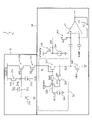
- FIG. 2 is a diagram showing a circuit configuration of the pixel 21 and the correction circuit 32. First, the circuit configuration of the pixel 21 will be described.
- the pixel 21 has a photodiode 211, a transfer transistor 212, an FD (Floating Diffusion) 213, a node 214, a reset transistor 215, an amplification transistor 216, a selection transistor 217, and an emission transistor 218.
- FD Floating Diffusion
- the photodiode 211 is an example of a photoelectric conversion element that converts incident light into electric charge and stores it by photoelectric conversion.
- the anode of the photodiode 211 is grounded and the cathode is connected to the transfer transistor 212 and the emission transistor 218.
- the transfer transistor 212 is composed of, for example, an N-channel MOSFET (Metal Oxide Semiconductor Field Effect Transistor).
- a transfer signal TRG is input from the vertical scanning circuit 10 to the gate of the transfer transistor 212.
- the transfer transistor 212 is driven based on the transfer signal TRG.
- the transfer transistor 212 is turned on, the electric charge stored in the photodiode 211 is transferred to the FD 213.
- the FD 213 is a floating diffusion region having a predetermined storage capacity connected to the gate of the amplification transistor 216.
- the electric charge transferred from the photodiode 211 is temporarily stored in the FD 213.
- the node 214 is a connection point between one end of the FD 213 and the gate of the amplification transistor 216.
- the charge stored in the FD 213 is transferred to the amplification transistor 216 via the node 214.
- the amplification transistor 216 is composed of, for example, an N-channel MOSFET.
- the amplification transistor 216 outputs a pixel signal indicating a level corresponding to the amount of charge stored in the FD 213, in other words, a level indicating the level of the voltage VFD of the node 214.
- the FD 213, the node 214, and the amplification transistor 216 function as a signal conversion unit that converts the electric charge stored in the photodiode 211 into a pixel signal at a level corresponding to the amount of the electric charge. Further, the node 214 can be boosted by making the voltage FDB at the other end of the FD 213 variable. As a result, the transfer efficiency of the charge stored in the photodiode 211 can be increased, and the saturated charge amount (Qs) can be further increased.
- the reset transistor 215 is composed of, for example, an N-channel MOSFET.
- a reset signal RST is input from the vertical scanning circuit 10 to the gate of the reset transistor 215.
- the reset transistor 215 is driven based on the reset signal RST.
- the reset transistor 215 is turned on, the electric charge stored in the node 214 is discharged to the power supply line VDDHPX, and the node 214 is reset.
- the reset transistor 215 switches from the on state to the off state.
- the selection transistor 217 is composed of, for example, an N-channel MOSFET.
- a selection signal SEL is input from the vertical scanning circuit 10 to the gate of the selection transistor 217.
- the selection transistor 217 switches whether or not to transmit an image signal to the signal processing circuit 30 based on the selection signal SEL.
- the selection transistor 217 is turned on, the pixel signal can be output to the signal processing circuit 30 through the signal line SL1.
- the selection transistor 217 is turned off, the transmission of the pixel signal through the signal line SL1 is cut off.
- the emission transistor 218 is composed of, for example, an N-channel MOSFET.
- the discharge transistor 218 is arranged in series between the photodiode 211 and the overflow drain OFD. Further, an emission signal OFG is input from the vertical scanning circuit 10 to the gate of the emission transistor 218. The emission transistor 218 is driven based on the emission signal OFG. When the emission transistor 218 is turned on, the electric charge accumulated in the photodiode 211 is discharged.
- the correction circuit 32 includes a first transistor 321, a second transistor 322, a first switch 323, a second switch 324, and a capacitor 325.
- the first transistor 321 is arranged between the selection transistor 217 and the non-inverting input terminal (+) of the comparator 31.
- the first transistor 321 is composed of, for example, an N-channel MOSFET, and the gate and drain are short-circuited. Further, the gate is connected to the first switch 323. The drain is connected to the source of the selection transistor 217. The source is connected to the non-inverting input terminal of the comparator 31 and is grounded via the transistor 340.
- the second transistor 322 is paired with the first transistor 321. That is, since the first transistor 321 and the second transistor 322 are manufactured to the same size by the same process, they have the same electrical characteristics.
- the threshold voltage between the gate and the source of the second transistor 322 is equivalent to the threshold voltage between the gate and the source of the first transistor 321. It is desirable that this threshold voltage is as low as possible in order to avoid narrowing the dynamic range of the signal line SL1.
- the first switch 323 is arranged between the gate of the first transistor 321 and the gate of the second transistor 322.
- the first transistor 321 performs switching operation based on the control signal SW0 input from the control circuit (not shown) of the signal processing circuit 30.
- the second switch is arranged between the source of the first transistor 321 and the source of the second transistor 322.
- the second transistor 322 is also driven based on the control signal SW1 input from the control circuit. When one of the first transistor 321 and the second transistor 322 is in the on state, the other is in the off state.
- One end of the capacitor 325 is connected to the gate of the second transistor 322, and the other end is grounded.
- the capacitor 325 is charged when the selection transistor 217 and the first switch 323 are on.
- the voltage of the signal line SL2 is held when the selection transistor 217 and the first switch 323 are in the off state and the second switch 324 is in the on state.
- the voltage of the signal line SL2 corresponds to the voltage of the inverting input terminal (+) of the comparator 31.
- the switch 341 is connected to the non-inverting input terminal (+) of the comparator 31, and the switch 342 is connected to the inverting input terminal (-).
- a transistor 343 is connected to the switch 341.
- the transistor 343 is a P-channel MOSFET. The drain of the transistor 343 is connected to the power supply line VDDHCM and the source is connected to the current source 344.
- the switch 342 is connected to the output terminal of the comparator 31. That is, in the comparator 31, the inverting input terminal ( ⁇ ) and the output terminal are connected to each other via the switch 342.
- the switch 341 and the switch 342 are driven based on the auto zero signal AZ input from the control circuit (not shown) of the signal processing circuit 30.
- FIG. 3 is a layout diagram showing an example of the positional relationship between the pixel array 20 and the signal processing circuit 30.
- the pixel array 20 is formed on the first semiconductor substrate (pixel chip) 110.
- a plurality of pixels 21 are arranged two-dimensionally.
- a second semiconductor substrate (logic chip) 120 is laminated on the first semiconductor substrate 110.
- the second semiconductor substrate 120 has a region 120a facing the pixel array 20.
- a signal processing circuit 30 is formed in this region 120a.
- the elements of the signal processing circuit 30 are arranged so as not to interfere with the light reception of the photodiode 211 of each pixel 21.
- the first semiconductor substrate 110 and the second semiconductor substrate 120 are joined to each other by, for example, a copper pad, a bump, or a TSV (Through Silicon Via).
- the pixel array 20 and the signal processing circuit 30 are not limited to the above-mentioned two-layer structure, and both may be formed on the first semiconductor substrate 110.
- the signal processing circuit 30 is arranged around the pixel array 20. When the pixel array 20 and the signal processing circuit 30 are formed on one semiconductor substrate in this way, the substrate bonding process becomes unnecessary.
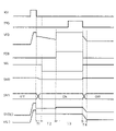
- FIG. 4 is a timing chart of the image pickup device 1 described above. Hereinafter, the operation of the image pickup apparatus 1 will be described with reference to FIG.
- the reset transistor 215 When the high-level reset signal RST is input to the gate of the reset transistor 215 of the pixel 21, the reset transistor 215 is turned on. As a result, the voltage VFD of the node 214 rises. At this time, the selection transistor 217 is also turned on based on the high-level selection signal SEL. Further, the first switch 323 of the correction circuit 32 is on based on the high level control signal SW0, and the second switch 324 is off based on the low level control signal SW1. Therefore, the voltage VHOLD of the capacitor 325 and the voltage VSL2 of the signal line SL2 also increase.
- the switch 341 and the switch 342 connected to the comparator 31 are turned on based on the high-level auto-zero signal.
- the switch 341 and the switch 342 switch from the on state to the off state.
- the comparator 31 outputs the comparison result between the pixel signal output from the pixel 21 after the reset signal RST and the lamp signal RAMP.
- This pixel signal contains only the charge component stored in advance in the FD 213, and does not include the charge component stored in the photodiode 211.
- the voltage VFD is boosted as the voltage FDB at the other end of the FD 213 is boosted.
- the selection transistor 217 is turned off based on the low-level selection signal SEL.
- the first switch 323 switches from the on state to the off state as the control signal SW0 changes from the high level to the low level.
- the second switch 324 switches from the off state to the on state as the control signal SW1 changes from the low level to the high level.
- the voltage of the signal line SL2 is held by the capacitor 325.
- the transfer transistor 212 is turned on based on the high-level transfer signal TRG.
- the electric charge stored in the photodiode 211 is transferred to the FD 213.
- the selection transistor 217 is switched from the off state to the on state, so that the pixel signal including the charge component stored in the photodiode 211 is sent to the non-inverting input terminal of the comparator 31 through the correction circuit 32. It is input to +).
- the comparator 31 outputs the result of comparing the pixel signal and the lamp signal to the latch circuit 33.
- the voltage VFD of the node 214 is boosted when the electric charge stored in the photodiode 211 is transferred to the FD 213. As a result, the charge transfer efficiency can be improved.
- the voltage VFD rises, the voltage VSL2 of the signal line SL2 also rises. If this amount of increase is large, a leak current may flow from the non-inverting input terminal (+) to the transistor 343 through the switch 341.
- the selection transistor 217 is in the off state during the FD boost period T3.
- the signal line SL1 is cut off, so that the potential increase of the non-inverting input terminal (+) of the comparator 31 can be avoided.
- the signal line SL1 is cut off, the potential of the non-inverting input terminal (+) drops. Therefore, the settling time for returning the potential increases, and there is a concern that the frame rate of the captured image may decrease.
- the correction circuit 32 is provided.
- the first switch 323 is in the on state and the second switch 324 is in the off state before the FD boost period T3.
- the voltage VSL2 of the signal line SL2 is represented by the following equation (1).
- VSL2 VSL1-Vth1 (1)
- VSL1 is the voltage of the signal line SL1
- Vth1 is the threshold voltage between the gate and the source of the first transistor 321.
- VSL2 VHOLD-Vth2 (2)
- VHOLD is the voltage of the capacitor 325
- Vth2 is the threshold voltage between the gate and the source of the second transistor 322.
- the capacitor 325 since the capacitor 325 is charged until it reaches the same potential as the voltage VSL1 before the FD boost period T3, the voltage VHOLD during the FD boost period T3 has the same potential as the voltage VSL1. Further, since the size of the second transistor 322 is the same as the size of the first transistor 321, the threshold voltage between the gate and the source of both transistors is also the same. As a result, the voltage VSL2 during the FD boost period T3 is maintained at the voltage before the FD boost period T3.
- the fluctuation of the voltage VSL2 during the FD boost period T3 can be suppressed. Therefore, it is possible to suppress a decrease in the frame rate of the captured image while improving the charge transfer efficiency from the photodiode 211 to the node 214.
- the threshold voltage Vth1 between the gate and the source of the first transistor 321 fluctuates due to temperature, manufacturing process, etc.
- this fluctuation is caused by the gate of the second transistor 322 in the correction circuit 32.
- It is offset by the threshold voltage Vth2 between the sources. Therefore, a power supply circuit that adjusts the voltage of the signal line VSL2 according to the fluctuation of the threshold voltage Vth1 becomes unnecessary. Therefore, it is possible to improve the charge transfer efficiency and suppress the decrease in the frame rate of the captured image at the same time with a simple and compact circuit configuration. Further, the power consumption can be reduced.
- FIG. 5 is a circuit diagram of the image pickup apparatus according to the second embodiment.
- the same components as those in the first embodiment are designated by the same reference numerals, and detailed description thereof will be omitted.
- the image pickup device 2 shown in FIG. 5 has a correction circuit 32a.
- the first switch 323 is composed of an N-channel MOSFET.
- the drain of the first switch 323 is connected to the gate of the first transistor 321 and the source is connected to the gate of the second transistor 322.
- the first switch 323 performs a switching operation based on the control signal SW0 input to the gate.
- FIG. 6 is a timing chart of the image pickup apparatus 2 according to the present embodiment. Hereinafter, the operation of the image pickup apparatus 1 will be described with reference to FIG. 6, focusing on the differences from the first embodiment.
- the selection transistor 217 is switched from the on state to the off state, the first switch 323 is switched from the on state to the off state, and the second switch 324 is switched from the off state to the on state. Switch to the state.
- the first switch 323 is composed of an N-channel MOSFET as described above. Therefore, the voltage VHOLD of the capacitor 325 is held at a potential lower than the voltage VSL1 of the signal line SL1 due to the influence of charge injection and feedthrough due to the falling edge of the signal. How much the voltage VHOLD is lower than the voltage VSL1 is determined by the ratio of the holding capacity of the capacitor 325 to the channel area of the first switch 323 and the falling slew rate of the first switch 323.
- the comparator 31 is stored in the photodiode 211 as in the first embodiment while maintaining the states of the selection transistor 217, the first switch 323, and the second switch 324.
- the comparison result between the pixel signal containing no charged charge component and the lamp signal RAMP is output.
- the selection transistor 217, the first switch 323, and the second switch 324 are maintained in the same state as the auto zero period T1.
- the states of the selection transistor 217, the first switch 323, and the second switch 324 are switched to the FD boost period T3 during the D phase period. That is, the selection transistor 217 is switched from the off state to the on state, the first switch 323 is switched from the off state to the on state, and the second switch 324 is switched from the on state to the off state.
- the correction circuit 32a has a correction function for sunspots by starting control for switching the states of the selection transistor 217, the first switch 323, and the second switch 324 from the auto zero period T1 as described above. Sunspots occur because a large amount of light enters the photodiode 211 and the voltage VFD and voltage VSL2 drop during the P-phase period T2. Sunspots affect the quality of the output image.
- the correction circuit 32a holds the voltage VSL2 immediately after the reset signal RST, that is, during the auto zero period T1. Therefore, the output image is not affected by sunspots.
- the voltage VHOLD is slightly lower than the voltage VSL1 due to the influence of charge injection and feedthrough. This amount of variation can also affect the quality of the output image. As a solution to this, for example, it is desirable to slow down the falling slew rate of the first switch 323. Further, it is desirable to set the voltage at the falling edge of the first switch 323 to a value slightly lower than the voltage VSL1 in the auto zero period T1 and the P phase period T2 instead of 0V in the P phase period T2 and the FD boost period T3. ..
- FIG. 7 is a circuit diagram of an image pickup device of the image pickup device according to the third embodiment.
- the same components as those in the first embodiment described above are designated by the same reference numerals, and detailed description thereof will be omitted.
- the image pickup apparatus 3 functions as a rolling shutter type image sensor having different timings for accumulating (exposing) charges among a plurality of pixels 21.
- the configuration of each pixel 21 is the same as that of the pixel 21 (see FIG. 3) described in the first embodiment except that it does not have the emission transistor 218.
- the operation in the auto zero period T1, the P phase period T2, the FD boost period T3, and the D phase period is the same as in the first embodiment. Therefore, the voltage VSL2 during the FD boost period T3 is held at the voltage of the P phase period T2 before the FD boost period T3. Therefore, also in this embodiment, it is possible to suppress a decrease in the frame rate while improving the charge transfer efficiency.
- control for switching each state of the selection transistor 217, the first switch 323, and the second switch 324 may be started from the auto zero period T1. In this case, it is possible to avoid deterioration of the quality of the output image with respect to sunspots.
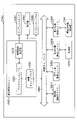
- FIG. 8 is a block diagram showing a configuration example of the ranging system according to the fourth embodiment.
- the distance measuring system 4 shown in FIG. 4 is a system for taking a distance image by using a ToF (Time of Flight) method, and includes a lighting device 41 and an image pickup device 42.
- ToF Time of Flight
- the lighting device 41 includes a lighting control unit 411 and a light emitting element 412.
- the illumination control unit 411 controls the pattern in which the light emitting element 412 irradiates the ranging light based on the control of the control unit 422. Specifically, the illumination control unit 411 controls the pattern in which the light emitting element 412 irradiates the ranging light according to the irradiation code included in the irradiation signal supplied from the control unit 422.
- the irradiation code consists of two values, "1" (High) and "0" (Low).
- the illumination control unit 411 turns on the light emitting element 412 when the value of the irradiation code is "1", and turns off the light emitting element 412 when the value of the irradiation code is "0".
- the light emitting element 412 emits range-finding light in a predetermined wavelength range based on the control of the illumination control unit 411.
- the light emitting element 412 is, for example, an infrared laser diode.
- the type of the light emitting element 412 and the wavelength range of the ranging light can be arbitrarily set according to the application of the ranging system 4.
- the image pickup device 42 receives the reflected light reflected by the subject 401 and the subject 402 for the distance measuring light.
- the image pickup device 42 includes an image pickup unit 421, a control unit 422, a display unit 423, and a storage unit 424.
- the image pickup unit 421 has a lens 431, a pixel array 432, and a signal processing circuit 433.
- the lens 431 forms an image of the incident light on the pixel array 432.
- the configuration of the lens 431 is arbitrary, and for example, the lens 431 can be configured by a plurality of lens groups.
- the pixel array 432 captures the subject 401, the subject 402, and the like based on the control of the control unit 422. Further, the pixel array 432 outputs the pixel signal obtained by imaging to the signal processing circuit 433.
- a plurality of pixels 21 are arranged two-dimensionally as in the pixel array 20 described in the first embodiment.
- the signal processing circuit 433 processes the pixel signal of the pixel array 432 based on the control of the control unit 422. For example, the signal processing circuit 433 detects the distance to the subject based on the pixel signal of the pixel array 432 and generates a distance image showing the distance to the subject.
- the comparator 31 and the correction circuit 32 described in the first embodiment are arranged.
- the control unit 422 is composed of, for example, a control circuit such as an FPGA (Field Programmable Gate Array), a DSP (Digital Signal Processor), a processor, or the like.
- the control unit 422 controls the illumination control unit 411, the pixel array 432, and the signal processing circuit 433.
- the display unit 423 includes, for example, a panel-type display device such as a liquid crystal display device or an organic EL (ElectroLuminescence) display device.
- a panel-type display device such as a liquid crystal display device or an organic EL (ElectroLuminescence) display device.
- the storage unit 424 can be configured by any storage device, storage medium, or the like, and stores a distance image or the like.
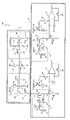
- FIG. 9 is a diagram showing a circuit configuration of the pixel 21 and the signal processing circuit 433 in this embodiment.
- the pixel 21 has a detection circuit 210a and a detection circuit 210b.
- the detection circuit 210a and the detection circuit 210b are connected to the cathode of the photodiode 211, respectively, and detect the charges accumulated in the photodiode 211 at different timings from each other.
- the detection circuit 210a includes a transfer transistor 212, an FD 213, a node 214, a reset transistor 215, an amplification transistor 216, and a selection transistor 217.
- the detection circuit 210b is paired with the detection circuit 210a and has a transfer transistor 212, an FD 213, a node 214, a reset transistor 215, an amplification transistor 216, and a selection transistor 217. Since these elements are described in detail in the first embodiment, the description thereof will be omitted.
- the correction circuit 32 is connected to the source of the selection transistor 217 of the detection circuit 210a and the detection circuit 210b, respectively. Since the circuit configuration of each correction circuit 32 is the same as that of the first embodiment, the description thereof will be omitted.
- each correction circuit 32 is connected to the non-inverting input terminal (+) of the comparator 31 as in the first embodiment. Further, a switch 341, a switch 342, a transistor 343, and a current source 344 are also provided around each comparator 31 as in the first embodiment.
- the pixel array 432 is formed on the first semiconductor substrate 110, and the signal processing circuit 433 is formed on the second semiconductor substrate 120 bonded to the first semiconductor substrate 110.
- the pixel array 432 and the signal processing circuit 433 are not limited to the above-mentioned two-layer structure, and both may be formed on the first semiconductor substrate 110.
- FIG. 10 is a timing chart of the distance measuring system 4 according to the present embodiment. Hereinafter, the operation of the ranging system 4 will be described with reference to FIG.
- the high-level reset signal RST is simultaneously input to the gates of the reset transistors 215 of the detection circuit 210a and the detection circuit 210b. At this time, since each reset transistor 215 is turned on, the voltage VFD0 of the node 214 of the detection circuit 210a and the voltage VFD1 of the node 214 of the detection circuit 210b rise.
- the high-level transfer signal TRG0 is input to the transfer transistor 212 of the detection circuit 210a at a predetermined cycle. Further, the high-level transfer signal TRG1 is input to the transfer transistor 212 of the detection circuit 210b at a predetermined cycle. The high-level transfer signal TRG0 and the high-level transfer signal TRG1 are alternately input to the transfer transistor 212 of each detection circuit.
- the period during which the transfer signal TRG0 is at a high level is the FD boost period T3a of the detection circuit 210a.
- the voltage VFD1 of the node 214 of the detection circuit 210b is boosted as the voltage FDB1 at the other end of the FD 213 is boosted in the detection circuit 210b. Therefore, the period during which the transfer signal TRG1 is at a high level is the FD boost period T3b of the detection circuit 210b.
- the first switch 323 Before the FD boost period T3a, in the correction circuit 32 connected to the detection circuit 210a, the first switch 323 is in the on state and the second switch 324 is in the off state. Further, during the FD boost period T3a, in the correction circuit 32, the first switch 323 is turned off and the second switch 324 is turned on. Therefore, as in the first embodiment, the voltage VSL2 during the FD boost period T3a is maintained at the voltage before the FD boost period T3a.
- the first switch 323 is in the on state and the second switch 324 is in the off state. Further, during the FD boost period T3b, in the correction circuit 32, the first switch 323 is turned off and the second switch 324 is turned on. Therefore, as in the first embodiment, the voltage VSL2 during the FD boost period T3b is also held at the voltage before the FD boost period T3b.
- the pixel signal output from the detection circuit 210a is read by the signal processing circuit 433 at the timing when the voltage VFD0 becomes lower than the predetermined value. Further, after the FD boost period T3b, the pixel signal output from the detection circuit 210b is read by the signal processing circuit 433 at the timing when the voltage VFD1 becomes lower than the predetermined value. After that, the distance from the distance measuring system 4 to the subjects 401 and 402 can be measured by calculating the difference between the image signals read by each detection circuit.
- the voltage fluctuation of the non-inverting input terminal (+) of the comparator 31 can be suppressed during the FD boost period, as in the other embodiments. Therefore, it is possible to suppress a decrease in the frame rate while improving the charge transfer efficiency.
- the technique according to the present disclosure can be applied to various products.
- the technology according to the present disclosure is realized as a device mounted on a moving body of any kind such as an automobile, an electric vehicle, a hybrid electric vehicle, a motorcycle, a bicycle, a personal mobility, an airplane, a drone, a ship, and a robot. You may.
- FIG. 11 is a block diagram showing a schematic configuration example of a vehicle control system, which is an example of a mobile control system to which the technique according to the present disclosure can be applied.
- the vehicle control system 12000 includes a plurality of electronic control units connected via the communication network 12001.
- the vehicle control system 12000 includes a drive system control unit 12010, a body system control unit 12020, an outside information detection unit 12030, an in-vehicle information detection unit 12040, and an integrated control unit 12050.
- a microcomputer 12051, an audio image output unit 12052, and an in-vehicle network I / F (Interface) 12053 are shown as a functional configuration of the integrated control unit 12050.
- the drive system control unit 12010 controls the operation of the device related to the drive system of the vehicle according to various programs.
- the drive system control unit 12010 has a driving force generator for generating a driving force of a vehicle such as an internal combustion engine or a driving motor, a driving force transmission mechanism for transmitting the driving force to the wheels, and a steering angle of the vehicle. It functions as a control device such as a steering mechanism for adjusting and a braking device for generating braking force of the vehicle.
- the body system control unit 12020 controls the operation of various devices mounted on the vehicle body according to various programs.
- the body system control unit 12020 functions as a keyless entry system, a smart key system, a power window device, or a control device for various lamps such as headlamps, back lamps, brake lamps, turn signals or fog lamps.
- the body system control unit 12020 may be input with radio waves transmitted from a portable device that substitutes for the key or signals of various switches.
- the body system control unit 12020 receives inputs of these radio waves or signals and controls a vehicle door lock device, a power window device, a lamp, and the like.
- the outside information detection unit 12030 detects information outside the vehicle equipped with the vehicle control system 12000.
- the image pickup unit 12031 is connected to the vehicle outside information detection unit 12030.
- the vehicle outside information detection unit 12030 causes the image pickup unit 12031 to capture an image of the outside of the vehicle and receives the captured image.
- the out-of-vehicle information detection unit 12030 may perform object detection processing or distance detection processing such as a person, a vehicle, an obstacle, a sign, or a character on the road surface based on the received image.
- the image pickup unit 12031 is an optical sensor that receives light and outputs an electric signal according to the amount of the light received.
- the image pickup unit 12031 can output an electric signal as an image or can output it as distance measurement information. Further, the light received by the image pickup unit 12031 may be visible light or invisible light such as infrared light.
- the in-vehicle information detection unit 12040 detects the in-vehicle information.
- a driver state detection unit 12041 that detects the driver's state is connected to the in-vehicle information detection unit 12040.
- the driver state detection unit 12041 includes, for example, a camera that images the driver, and the in-vehicle information detection unit 12040 determines the degree of fatigue or concentration of the driver based on the detection information input from the driver state detection unit 12041. It may be calculated, or it may be determined whether the driver has fallen asleep.
- the microcomputer 12051 calculates the control target value of the driving force generator, the steering mechanism, or the braking device based on the information inside and outside the vehicle acquired by the vehicle exterior information detection unit 12030 or the vehicle interior information detection unit 12040, and the drive system control unit.
- a control command can be output to 12010.
- the microcomputer 12051 realizes ADAS (Advanced Driver Assistance System) functions including vehicle collision avoidance or impact mitigation, follow-up driving based on inter-vehicle distance, vehicle speed maintenance driving, vehicle collision warning, vehicle lane deviation warning, and the like. It is possible to perform cooperative control for the purpose of.
- ADAS Advanced Driver Assistance System
- the microcomputer 12051 controls the driving force generating device, the steering mechanism, the braking device, and the like based on the information around the vehicle acquired by the vehicle exterior information detection unit 12030 or the vehicle interior information detection unit 12040. It is possible to perform coordinated control for the purpose of automatic driving that runs autonomously without depending on the operation.
- the microcomputer 12051 can output a control command to the body system control unit 12030 based on the information outside the vehicle acquired by the vehicle outside information detection unit 12030.
- the microcomputer 12051 controls the headlamps according to the position of the preceding vehicle or the oncoming vehicle detected by the outside information detection unit 12030, and performs cooperative control for the purpose of anti-glare such as switching the high beam to the low beam. It can be carried out.
- the audio image output unit 12052 transmits an output signal of at least one of audio and an image to an output device capable of visually or audibly notifying information to the passenger or the outside of the vehicle.
- an audio speaker 12061, a display unit 12062, and an instrument panel 12063 are exemplified as output devices.
- the display unit 12062 may include, for example, at least one of an onboard display and a heads-up display.
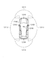
- FIG. 12 is a diagram showing an example of the installation position of the imaging unit 12031.
- the image pickup units 12101, 12102, 12103, 12104, and 12105 are provided.
- the image pickup units 12101, 12102, 12103, 12104, 12105 are provided at positions such as, for example, the front nose, side mirrors, rear bumpers, back doors, and the upper part of the windshield in the vehicle interior of the vehicle 12100.
- the image pickup unit 12101 provided on the front nose and the image pickup section 12105 provided on the upper part of the windshield in the vehicle interior mainly acquire an image in front of the vehicle 12100.
- the image pickup units 12102 and 12103 provided in the side mirror mainly acquire images of the side of the vehicle 12100.
- the image pickup unit 12104 provided in the rear bumper or the back door mainly acquires an image of the rear of the vehicle 12100.
- the image pickup unit 12105 provided on the upper part of the windshield in the vehicle interior is mainly used for detecting a preceding vehicle, a pedestrian, an obstacle, a traffic light, a traffic sign, a lane, or the like.
- FIG. 12 shows an example of the shooting range of the imaging units 12101 to 12104.
- the imaging range 12111 indicates the imaging range of the imaging unit 12101 provided on the front nose
- the imaging range 1211212113 indicates the imaging range of the imaging units 12102 and 12103 provided on the side mirrors, respectively
- the imaging range 12114 indicates the rear bumper or the rear bumper.
- the imaging range of the imaging unit 12104 provided on the back door is shown. For example, by superimposing the image data captured by the imaging units 12101 to 12104, a bird's-eye view image of the vehicle 12100 can be obtained.
- At least one of the image pickup units 12101 to 12104 may have a function of acquiring distance information.
- at least one of the image pickup units 12101 to 12104 may be a stereo camera including a plurality of image pickup elements, or may be an image pickup element having pixels for phase difference detection.
- the microcomputer 12051 has a distance to each three-dimensional object within the imaging range 12111 to 12114 based on the distance information obtained from the imaging unit 12101 to 12104, and a temporal change of this distance (relative speed with respect to the vehicle 12100). By obtaining can. Further, the microcomputer 12051 can set an inter-vehicle distance to be secured in advance in front of the preceding vehicle, and can perform automatic braking control (including follow-up stop control), automatic acceleration control (including follow-up start control), and the like. In this way, it is possible to perform coordinated control for the purpose of automatic driving or the like in which the vehicle runs autonomously without depending on the operation of the driver.
- automatic braking control including follow-up stop control
- automatic acceleration control including follow-up start control
- the microcomputer 12051 converts three-dimensional object data related to a three-dimensional object into two-wheeled vehicles, ordinary vehicles, large vehicles, pedestrians, electric poles, and other three-dimensional objects based on the distance information obtained from the image pickup units 12101 to 12104. It can be classified and extracted and used for automatic avoidance of obstacles. For example, the microcomputer 12051 distinguishes obstacles around the vehicle 12100 into obstacles that are visible to the driver of the vehicle 12100 and obstacles that are difficult to see. Then, the microcomputer 12051 determines the collision risk indicating the risk of collision with each obstacle, and when the collision risk is equal to or higher than the set value and there is a possibility of collision, the microcomputer 12051 via the audio speaker 12061 or the display unit 12062. By outputting an alarm to the driver and performing forced deceleration and avoidance steering via the drive system control unit 12010, driving support for collision avoidance can be provided.
- At least one of the image pickup units 12101 to 12104 may be an infrared camera that detects infrared rays.
- the microcomputer 12051 can recognize a pedestrian by determining whether or not a pedestrian is present in the captured image of the imaging unit 12101 to 12104.
- recognition of a pedestrian is, for example, a procedure for extracting feature points in an image captured by an image pickup unit 12101 to 12104 as an infrared camera, and a pattern matching process for a series of feature points showing the outline of an object to determine whether or not the pedestrian is a pedestrian. It is done by the procedure to determine.
- the audio image output unit 12052 determines the square contour line for emphasizing the recognized pedestrian.
- the display unit 12062 is controlled so as to superimpose and display. Further, the audio image output unit 12052 may control the display unit 12062 so as to display an icon or the like indicating a pedestrian at a desired position.
- the above is an example of a vehicle control system to which the technique according to the present disclosure can be applied.
- the technique according to the present disclosure may be applied to, for example, the image pickup unit 12031 among the configurations described above.
- the image pickup unit 421 can be applied to the image pickup unit 12031.
- the present technology can have the following configurations.
- Photoelectric conversion element and A signal conversion unit that is boosted when converting the charge transferred from the photoelectric conversion element into a pixel signal, and A selection transistor that cuts off the signal line of the pixel signal during the boosting period of the signal conversion unit. It has a non-inverting input terminal to which the pixel signal is input via the selection transistor, an inverting input terminal to which a lamp signal is input, and an output terminal for outputting a comparison result between the pixel signal and the lamp signal.
- An image pickup apparatus comprising a correction circuit for holding the potential of the non-inverting input terminal during the boosting period to the potential of the non-inverting input terminal before the boosting period.
- the correction circuit is A first transistor arranged between the selection transistor and the non-inverting input terminal, The first transistor, the pair of second transistors, and A first switch arranged between the gate of the first transistor and the gate of the second transistor, A second switch arranged between the source of the first transistor and the source of the second transistor, With a capacitor connected to the gate of the second transistor,
- the image pickup apparatus according to (1) wherein the first switch is in the off state and the second switch is in the on state during the boosting period.
- the threshold voltage between the gate and the source of the first transistor is equivalent to the threshold voltage between the gate and the source of the second transistor.
- the photoelectric conversion element, the signal conversion unit, and the selection transistor are arranged on the first semiconductor substrate, and the comparator and the correction circuit are arranged on the second semiconductor substrate laminated on the first semiconductor substrate. , (1).
- the signal processing circuit is a column ADC (Analog to Digital Converter) that processes the pixel signal for each row of the plurality of pixels.
- the image pickup apparatus which is a rolling shutter system in which the plurality of photoelectric conversion elements accumulate the electric charges at different timings.
- a lighting device that irradiates range-finding light, An image pickup device that receives the reflected light of the distance measuring light is provided.
- the image pickup device A photoelectric conversion element that photoelectrically converts the reflected light and A signal conversion unit that is boosted when converting the charge transferred from the photoelectric conversion element into a pixel signal, and A selection transistor that cuts off the signal line of the pixel signal during the boosting period of the signal conversion unit.
- It has a non-inverting input terminal to which the pixel signal is input via the selection transistor, an inverting input terminal to which a lamp signal is input, and an output terminal for outputting a comparison result between the pixel signal and the lamp signal.
- a comparator A ranging system comprising a correction circuit for holding the potential of the non-inverting input terminal during the boosting period to the potential of the non-inverting input terminal before the boosting period.
- the correction circuit is A first transistor arranged between the selection transistor and the non-inverting input terminal, The first transistor, the pair of second transistors, and A first switch arranged between the gate of the first transistor and the gate of the second transistor, A second switch arranged between the source of the first transistor and the source of the second transistor, With a capacitor connected to the gate of the second transistor,
- the distance measuring system according to (12) wherein the first switch is in the off state and the second switch is in the on state during the boosting period.
- the threshold voltage between the gate and the source of the first transistor is equivalent to the threshold voltage between the gate and the source of the second transistor.
- Image pickup device 4 Distance measurement system 20: Pixel array 21: Pixel 30: Signal processing circuit 31: Comparator 32, 32a: Correction circuit 41: Lighting device 42: Image pickup device 110: First semiconductor substrate 120: Second Semiconductor substrate 211: Photodiode 213: FD 214: Node 216: Amplification transistor 217: Selective transistor 3211: First transistor 322: Second transistor 323: First switch 324: Second switch 325: Capacitor 432: Pixel array 433: Signal processing circuit
Landscapes
- Engineering & Computer Science (AREA)
- Multimedia (AREA)
- Signal Processing (AREA)
- Theoretical Computer Science (AREA)
- Transforming Light Signals Into Electric Signals (AREA)
- Analogue/Digital Conversion (AREA)
Abstract
Description
前記選択トランジスタと前記非反転入力端子との間に配置された第1トランジスタと、
前記第1トランジスタと一対の第2トランジスタと、
前記第1トランジスタのゲートと前記第2トランジスタのゲートとの間に配置された第1スイッチと、
前記第1トランジスタのソースと前記第2トランジスタのソースとの間に配置された第2スイッチと、
前記第2トランジスタのゲートに接続されたキャパシタと、を有し、
前記昇圧期間に、前記第1スイッチはオフ状態であるとともに前記第2スイッチはオン状態であってもよい。
前記コンパレータおよび前記補正回路が、前記光電変換素子ごとに設けられてもよい。
前記選択トランジスタと前記非反転入力端子との間に配置された第1トランジスタと、
前記第1トランジスタと一対の第2トランジスタと、
前記第1トランジスタのゲートと前記第2トランジスタのゲートとの間に配置された第1スイッチと、
前記第1トランジスタのソースと前記第2トランジスタのソースとの間に配置された第2スイッチと、
前記第2トランジスタのゲートに接続されたキャパシタと、を有し、
前記昇圧期間に、前記第1スイッチはオフ状態であるとともに前記第2スイッチはオン状態であってもよい。
図1は、第1実施形態に係る撮像装置の構成を示す図である。図1に示す撮像装置1は、垂直走査回路10と、画素アレイ20と、信号処理回路30と、水平転送走査回路40と、を備える。
VSL2=VSL1-Vth1 (1)
式(1)において、VSL1は信号線SL1の電圧であり、Vth1は第1トランジスタ321のゲート-ソース間のしきい値電圧である。
VSL2=VHOLD-Vth2 (2)
式(2)において、VHOLDはキャパシタ325の電圧であり、Vth2は、第2トランジスタ322のゲート-ソース間のしきい値電圧である。
図5は、第2実施形態に係る撮像装置の回路図である。第1実施形態と同様の構成要素には同じ符号を付し、詳細な説明を省略する。
図7は、第3実施形態に係る撮像装置の撮像装置の回路図である。上述した第1実施形態と同様の構成要素には、同じ符号を付し、詳細な説明を省略する。
図8は、第4実施形態に係る測距システムの構成例を示すブロック図である。図4に示す測距システム4は、ToF(Time of Flight)法を用いて距離画像の撮影を行うシステムであり、照明装置41および撮像装置42を備える。
本開示に係る技術(本技術)は、様々な製品へ応用することができる。例えば、本開示に係る技術は、自動車、電気自動車、ハイブリッド電気自動車、自動二輪車、自転車、パーソナルモビリティ、飛行機、ドローン、船舶、ロボット等のいずれかの種類の移動体に搭載される装置として実現されてもよい。
(1) 光電変換素子と、
前記光電変換素子から転送された電荷を画素信号に変換するときに昇圧される信号変換部と、
前記信号変換部の昇圧期間に、前記画素信号の信号線を遮断する選択トランジスタと、
前記選択トランジスタを介して前記画素信号が入力される非反転入力端子と、ランプ信号が入力される反転入力端子と、前記画素信号と前記ランプ信号との比較結果を出力する出力端子と、を有するコンパレータと、
前記昇圧期間における前記非反転入力端子の電位を、前記昇圧期間前の前記非反転入力端子の電位に保持する補正回路と、を有する、撮像装置。
(2) 前記補正回路は、
前記選択トランジスタと前記非反転入力端子との間に配置された第1トランジスタと、
前記第1トランジスタと一対の第2トランジスタと、
前記第1トランジスタのゲートと前記第2トランジスタのゲートとの間に配置された第1スイッチと、
前記第1トランジスタのソースと前記第2トランジスタのソースとの間に配置された第2スイッチと、
前記第2トランジスタのゲートに接続されたキャパシタと、を有し、
前記昇圧期間に、前記第1スイッチはオフ状態であるとともに前記第2スイッチはオン状態である、(1)に記載の撮像装置。
(3) 前記第1トランジスタのゲート-ソース間のしきい値電圧が、前記第2トランジスタのゲート-ソース間のしきい値電圧と同等である、(2)に記載の撮像装置。
(4) 前記昇圧期間の直前に、前記第1スイッチはオン状態からオフ状態に切り替わるとともに、前記第2スイッチはオフ状態からオン状態に切り替わる、(2)に記載の撮像装置。
(5) 前記昇圧期間よりも前の前記コンパレータのオートゼロ期間に、前記選択トランジスタがオン状態からオフ状態に切り替わり、前記第1スイッチがオン状態からオフ状態に切り替わり、前記第2スイッチがオフ状態からオン状態に切り替わる、(2)に記載の撮像装置。
(6) 前記第1スイッチが、Nチャネル型MOSFETである、(5)に記載の撮像装置。
(7) 前記光電変換素子、前記信号変換部、および前記選択トランジスタが第1半導体基板に配置され、前記コンパレータおよび前記補正回路が前記第1半導体基板に積層される第2半導体基板に配置される、(1)に記載の撮像装置。
(8) 前記光電変換素子、前記信号変換部、前記選択トランジスタ、前記コンパレータ、および前記補正回路が、一つの半導体基板に配置される、(1)に記載の撮像装置。
(9) 前記信号処理回路が、前記複数の画素の列ごとに前記画素信号を処理するカラムADC(Analog to Digital Converter)である、(1)に記載の撮像装置。
(10) 前記前記複数の光電変換素子が同じタイミングで前記電荷を蓄積するグローバルシャッタ方式である、(9)に記載の撮像装置。
(11) 前記前記複数の光電変換素子が異なるタイミングで前記電荷を蓄積するローリングシャッタ方式である、(9)に記載の撮像装置。
(12) 測距光を照射する照明装置と、
前記測距光の反射光を受光する撮像装置と、を備え、
前記撮像装置が、
前記反射光を光電変換する光電変換素子と、
前記光電変換素子から転送された電荷を画素信号に変換するときに昇圧される信号変換部と、
前記信号変換部の昇圧期間に、前記画素信号の信号線を遮断する選択トランジスタと、
前記選択トランジスタを介して前記画素信号が入力される非反転入力端子と、ランプ信号が入力される反転入力端子と、前記画素信号と前記ランプ信号との比較結果を出力する出力端子と、を有するコンパレータと、
前記昇圧期間における前記非反転入力端子の電位を、前記昇圧期間前の前記非反転入力端子の電位に保持する補正回路と、を有する、測距システム。
(13) 前記補正回路は、
前記選択トランジスタと前記非反転入力端子との間に配置された第1トランジスタと、
前記第1トランジスタと一対の第2トランジスタと、
前記第1トランジスタのゲートと前記第2トランジスタのゲートとの間に配置された第1スイッチと、
前記第1トランジスタのソースと前記第2トランジスタのソースとの間に配置された第2スイッチと、
前記第2トランジスタのゲートに接続されたキャパシタと、を有し、
前記昇圧期間に、前記第1スイッチはオフ状態であるとともに前記第2スイッチはオン状態である、(12)に記載の測距システム。
(14) 前記第1トランジスタのゲート-ソース間のしきい値電圧が、前記第2トランジスタのゲート-ソース間のしきい値電圧と同等である、(13)に記載の測距システム。
(15) 前記昇圧期間の直前に、前記第1スイッチはオン状態からオフ状態に切り替わるとともに、前記第2スイッチはオフ状態からオン状態に切り替わる、(13)に記載の測距システム。
(16) 前記光電変換素子、前記信号変換部、および前記選択トランジスタが第1半導体基板に配置され、前記コンパレータおよび前記補正回路が前記第1半導体基板に積層される第2半導体基板に配置される、(12)に記載の測距システム。
(17) 前記光電変換素子、前記信号変換部、前記選択トランジスタ、前記コンパレータ、および前記補正回路が、一つの半導体基板に配置される、(12)に記載の測距システム。
4:測距システム
20:画素アレイ
21:画素
30:信号処理回路
31:コンパレータ
32、32a:補正回路
41:照明装置
42:撮像装置
110:第1半導体基板
120:第2半導体基板
211:フォトダイオード
213:FD
214:ノード
216:増幅トランジスタ
217:選択トランジスタ
321:第1トランジスタ
322:第2トランジスタ
323:第1スイッチ
324:第2スイッチ
325:キャパシタ
432:画素アレイ
433:信号処理回路
Claims (17)
- 光電変換素子と、
前記光電変換素子から転送された電荷を画素信号に変換するときに昇圧される信号変換部と、
前記信号変換部の昇圧期間に、前記画素信号の信号線を遮断する選択トランジスタと、
前記選択トランジスタを介して前記画素信号が入力される非反転入力端子と、ランプ信号が入力される反転入力端子と、前記画素信号と前記ランプ信号との比較結果を出力する出力端子と、を有するコンパレータと、
前記昇圧期間における前記非反転入力端子の電位を、前記昇圧期間前の前記非反転入力端子の電位に保持する補正回路と、を備える、撮像装置。 - 前記補正回路は、
前記選択トランジスタと前記非反転入力端子との間に配置された第1トランジスタと、
前記第1トランジスタと一対の第2トランジスタと、
前記第1トランジスタのゲートと前記第2トランジスタのゲートとの間に配置された第1スイッチと、
前記第1トランジスタのソースと前記第2トランジスタのソースとの間に配置された第2スイッチと、
前記第2トランジスタのゲートに接続されたキャパシタと、を有し、
前記昇圧期間に、前記第1スイッチはオフ状態であるとともに前記第2スイッチはオン状態である、請求項1に記載の撮像装置。 - 前記第1トランジスタのゲート-ソース間のしきい値電圧が、前記第2トランジスタのゲート-ソース間のしきい値電圧と同等である、請求項2に記載の撮像装置。
- 前記昇圧期間の直前に、前記第1スイッチはオン状態からオフ状態に切り替わるとともに、前記第2スイッチはオフ状態からオン状態に切り替わる、請求項2に記載の撮像装置。
- 前記昇圧期間よりも前の前記コンパレータのオートゼロ期間に、前記選択トランジスタがオン状態からオフ状態に切り替わり、前記第1スイッチがオン状態からオフ状態に切り替わり、前記第2スイッチがオフ状態からオン状態に切り替わる、請求項2に記載の撮像装置。
- 前記第1スイッチが、Nチャネル型MOSFETである、請求項5に記載の撮像装置。
- 前記光電変換素子、前記信号変換部、および前記選択トランジスタが第1半導体基板に配置され、前記コンパレータおよび前記補正回路が前記第1半導体基板に積層される第2半導体基板に配置される、請求項1に記載の撮像装置。
- 前記光電変換素子、前記信号変換部、前記選択トランジスタ、前記コンパレータ、および前記補正回路が、一つの半導体基板に配置される、請求項1に記載の撮像装置。
- 複数の前記光電変換素子が二次元状に配置され、
前記コンパレータおよび前記補正回路が、前記光電変換素子ごとに設けられている、請求項1に記載の撮像装置。 - 前記前記複数の光電変換素子が同じタイミングで前記電荷を蓄積するグローバルシャッタ方式である、請求項9に記載の撮像装置。
- 前記前記複数の光電変換素子が異なるタイミングで前記電荷を蓄積するローリングシャッタ方式である、請求項9に記載の撮像装置。
- 測距光を照射する照明装置と、
前記測距光の反射光を受光する撮像装置と、を備え、
前記撮像装置が、
前記反射光を光電変換する光電変換素子と、
前記光電変換素子から転送された電荷を画素信号に変換するときに昇圧される信号変換部と、
前記信号変換部の昇圧期間に、前記画素信号の信号線を遮断する選択トランジスタと、
前記選択トランジスタを介して前記画素信号が入力される非反転入力端子と、ランプ信号が入力される反転入力端子と、前記画素信号と前記ランプ信号との比較結果を出力する出力端子と、を有するコンパレータと、
前記昇圧期間における前記非反転入力端子の電位を、前記昇圧期間前の前記非反転入力端子の電位に保持する補正回路と、を有する、測距システム。 - 前記補正回路は、
前記選択トランジスタと前記非反転入力端子との間に配置された第1トランジスタと、
前記第1トランジスタと一対の第2トランジスタと、
前記第1トランジスタのゲートと前記第2トランジスタのゲートとの間に配置された第1スイッチと、
前記第1トランジスタのソースと前記第2トランジスタのソースとの間に配置された第2スイッチと、
前記第2トランジスタのゲートに接続されたキャパシタと、を有し、
前記昇圧期間に、前記第1スイッチはオフ状態であるとともに前記第2スイッチはオン状態である、請求項12に記載の測距システム。 - 前記第1トランジスタのゲート-ソース間のしきい値電圧が、前記第2トランジスタのゲート-ソース間のしきい値電圧と同等である、請求項13に記載の測距システム。
- 前記昇圧期間の直前に、前記第1スイッチはオン状態からオフ状態に切り替わるとともに、前記第2スイッチはオフ状態からオン状態に切り替わる、請求項13に記載の測距システム。
- 前記光電変換素子、前記信号変換部、および前記選択トランジスタが第1半導体基板に配置され、前記コンパレータおよび前記補正回路が前記第1半導体基板に積層される第2半導体基板に配置される、請求項12に記載の測距システム。
- 前記光電変換素子、前記信号変換部、前記選択トランジスタ、前記コンパレータ、および前記補正回路が、一つの半導体基板に配置される、請求項12に記載の測距システム。
Priority Applications (2)
| Application Number | Priority Date | Filing Date | Title |
|---|---|---|---|
| US18/259,334 US12284456B2 (en) | 2021-01-05 | 2021-12-06 | Imaging device and distance measurement system |
| US19/173,054 US20250240543A1 (en) | 2021-01-05 | 2025-04-08 | Imaging device and distance measurement system |
Applications Claiming Priority (2)
| Application Number | Priority Date | Filing Date | Title |
|---|---|---|---|
| JP2021-000561 | 2021-01-05 | ||
| JP2021000561A JP2022105924A (ja) | 2021-01-05 | 2021-01-05 | 撮像装置および測距システム |
Related Child Applications (2)
| Application Number | Title | Priority Date | Filing Date |
|---|---|---|---|
| US18/259,334 A-371-Of-International US12284456B2 (en) | 2021-01-05 | 2021-12-06 | Imaging device and distance measurement system |
| US19/173,054 Continuation US20250240543A1 (en) | 2021-01-05 | 2025-04-08 | Imaging device and distance measurement system |
Publications (1)
| Publication Number | Publication Date |
|---|---|
| WO2022149388A1 true WO2022149388A1 (ja) | 2022-07-14 |
Family
ID=82357340
Family Applications (1)
| Application Number | Title | Priority Date | Filing Date |
|---|---|---|---|
| PCT/JP2021/044739 Ceased WO2022149388A1 (ja) | 2021-01-05 | 2021-12-06 | 撮像装置および測距システム |
Country Status (3)
| Country | Link |
|---|---|
| US (2) | US12284456B2 (ja) |
| JP (1) | JP2022105924A (ja) |
| WO (1) | WO2022149388A1 (ja) |
Cited By (1)
| Publication number | Priority date | Publication date | Assignee | Title |
|---|---|---|---|---|
| WO2024096095A1 (ja) * | 2022-11-02 | 2024-05-10 | ソニーセミコンダクタソリューションズ株式会社 | 撮像素子、電子機器 |
Families Citing this family (1)
| Publication number | Priority date | Publication date | Assignee | Title |
|---|---|---|---|---|
| WO2025249098A1 (ja) * | 2024-05-30 | 2025-12-04 | ソニーセミコンダクタソリューションズ株式会社 | センシングデバイス、電子機器およびセンシングデバイスの制御方法 |
Citations (4)
| Publication number | Priority date | Publication date | Assignee | Title |
|---|---|---|---|---|
| JP2001298662A (ja) * | 2000-04-12 | 2001-10-26 | Innotech Corp | 固体撮像装置及びその駆動方法 |
| JP2005323331A (ja) * | 2004-02-23 | 2005-11-17 | Sony Corp | Ad変換方法およびad変換装置並びに物理量分布検知の半導体装置および電子機器 |
| JP2008544656A (ja) * | 2005-06-14 | 2008-12-04 | マイクロン テクノロジー, インク. | ピクセル個別黒点状不具合防止回路とその動作態様 |
| US20190306445A1 (en) * | 2018-03-29 | 2019-10-03 | SK Hynix Inc. | Electronic device |
Family Cites Families (3)
| Publication number | Priority date | Publication date | Assignee | Title |
|---|---|---|---|---|
| KR102540242B1 (ko) * | 2018-01-12 | 2023-06-02 | 삼성전자주식회사 | 이미지 센서 |
| KR102921314B1 (ko) * | 2019-07-24 | 2026-02-04 | 삼성전자주식회사 | 이미지 센서 |
| US11356626B2 (en) * | 2020-04-22 | 2022-06-07 | Omnivision Technologies, Inc. | Flexible exposure control for image sensors with phase detection auto focus pixels |
-
2021
- 2021-01-05 JP JP2021000561A patent/JP2022105924A/ja active Pending
- 2021-12-06 US US18/259,334 patent/US12284456B2/en active Active
- 2021-12-06 WO PCT/JP2021/044739 patent/WO2022149388A1/ja not_active Ceased
-
2025
- 2025-04-08 US US19/173,054 patent/US20250240543A1/en active Pending
Patent Citations (4)
| Publication number | Priority date | Publication date | Assignee | Title |
|---|---|---|---|---|
| JP2001298662A (ja) * | 2000-04-12 | 2001-10-26 | Innotech Corp | 固体撮像装置及びその駆動方法 |
| JP2005323331A (ja) * | 2004-02-23 | 2005-11-17 | Sony Corp | Ad変換方法およびad変換装置並びに物理量分布検知の半導体装置および電子機器 |
| JP2008544656A (ja) * | 2005-06-14 | 2008-12-04 | マイクロン テクノロジー, インク. | ピクセル個別黒点状不具合防止回路とその動作態様 |
| US20190306445A1 (en) * | 2018-03-29 | 2019-10-03 | SK Hynix Inc. | Electronic device |
Cited By (1)
| Publication number | Priority date | Publication date | Assignee | Title |
|---|---|---|---|---|
| WO2024096095A1 (ja) * | 2022-11-02 | 2024-05-10 | ソニーセミコンダクタソリューションズ株式会社 | 撮像素子、電子機器 |
Also Published As
| Publication number | Publication date |
|---|---|
| US12284456B2 (en) | 2025-04-22 |
| US20250240543A1 (en) | 2025-07-24 |
| JP2022105924A (ja) | 2022-07-15 |
| US20240314467A1 (en) | 2024-09-19 |
Similar Documents
| Publication | Publication Date | Title |
|---|---|---|
| WO2019146527A1 (ja) | 固体撮像素子、撮像装置、および、固体撮像素子の制御方法 | |
| US12164029B2 (en) | Time measurement device and time measurement apparatus | |
| JP6953274B2 (ja) | 撮像システム及び撮像装置 | |
| US20250240543A1 (en) | Imaging device and distance measurement system | |
| JPWO2018207661A1 (ja) | 光センサ、及び、電子機器 | |
| WO2022270034A1 (ja) | 撮像装置、電子機器、および光検出方法 | |
| CN110226325B (zh) | 摄像系统和摄像装置 | |
| JP7071292B2 (ja) | 撮像システム、撮像装置、及び制御装置 | |
| US20250113114A1 (en) | Solid-state imaging element, method for controlling solid-state imaging element, and electronic device | |
| US12267609B2 (en) | Solid-state imaging device | |
| JP2023040318A (ja) | 撮像回路および撮像装置 | |
| US20250350862A1 (en) | Imaging device and photodetection device | |
| WO2020149095A1 (ja) | 撮像装置および撮像システム | |
| WO2022153746A1 (ja) | 撮像装置 | |
| WO2022196139A1 (ja) | 撮像装置および撮像システム | |
| TW202209868A (zh) | 固態攝像元件、感測系統及固態攝像元件之控制方法 | |
| WO2021261079A1 (ja) | 光検出装置および測距システム | |
| US12273636B2 (en) | Photodetection device and electronic apparatus | |
| US20250227390A1 (en) | Linear sensor | |
| JP2020141362A (ja) | 光検出装置 | |
| WO2024180928A1 (ja) | 固体撮像素子 | |
| KR20260003001A (ko) | 촬상 장치 | |
| WO2023089958A1 (ja) | 固体撮像素子 | |
| WO2025004802A1 (ja) | 撮像装置 | |
| WO2024202651A1 (ja) | 光検出装置および測距システム |
Legal Events
| Date | Code | Title | Description |
|---|---|---|---|
| 121 | Ep: the epo has been informed by wipo that ep was designated in this application |
Ref document number: 21917609 Country of ref document: EP Kind code of ref document: A1 |
|
| WWE | Wipo information: entry into national phase |
Ref document number: 18259334 Country of ref document: US |
|
| NENP | Non-entry into the national phase |
Ref country code: DE |
|
| 122 | Ep: pct application non-entry in european phase |
Ref document number: 21917609 Country of ref document: EP Kind code of ref document: A1 |
|
| WWG | Wipo information: grant in national office |
Ref document number: 18259334 Country of ref document: US |