WO2022149236A1 - 光通信システム、制御回路、記憶媒体および光通信方法 - Google Patents
光通信システム、制御回路、記憶媒体および光通信方法 Download PDFInfo
- Publication number
- WO2022149236A1 WO2022149236A1 PCT/JP2021/000339 JP2021000339W WO2022149236A1 WO 2022149236 A1 WO2022149236 A1 WO 2022149236A1 JP 2021000339 W JP2021000339 W JP 2021000339W WO 2022149236 A1 WO2022149236 A1 WO 2022149236A1
- Authority
- WO
- WIPO (PCT)
- Prior art keywords
- optical
- signal
- transmission
- signals
- packet
- Prior art date
- Legal status (The legal status is an assumption and is not a legal conclusion. Google has not performed a legal analysis and makes no representation as to the accuracy of the status listed.)
- Ceased
Links
Images






Classifications
-
- H—ELECTRICITY
- H04—ELECTRIC COMMUNICATION TECHNIQUE
- H04J—MULTIPLEX COMMUNICATION
- H04J14/00—Optical multiplex systems
- H04J14/08—Time-division multiplex systems
- H04J14/086—Medium access
-
- H—ELECTRICITY
- H04—ELECTRIC COMMUNICATION TECHNIQUE
- H04B—TRANSMISSION
- H04B10/00—Transmission systems employing electromagnetic waves other than radio-waves, e.g. infrared, visible or ultraviolet light, or employing corpuscular radiation, e.g. quantum communication
- H04B10/25—Arrangements specific to fibre transmission
- H04B10/2575—Radio-over-fibre, e.g. radio frequency signal modulated onto an optical carrier
- H04B10/25752—Optical arrangements for wireless networks
- H04B10/25758—Optical arrangements for wireless networks between a central unit and a single remote unit by means of an optical fibre
- H04B10/25759—Details of the reception of RF signal or the optical conversion before the optical fibre
-
- H—ELECTRICITY
- H04—ELECTRIC COMMUNICATION TECHNIQUE
- H04B—TRANSMISSION
- H04B10/00—Transmission systems employing electromagnetic waves other than radio-waves, e.g. infrared, visible or ultraviolet light, or employing corpuscular radiation, e.g. quantum communication
- H04B10/60—Receivers
- H04B10/61—Coherent receivers
- H04B10/614—Coherent receivers comprising one or more polarization beam splitters, e.g. polarization multiplexed [PolMux] X-PSK coherent receivers, polarization diversity heterodyne coherent receivers
-
- H—ELECTRICITY
- H04—ELECTRIC COMMUNICATION TECHNIQUE
- H04B—TRANSMISSION
- H04B10/00—Transmission systems employing electromagnetic waves other than radio-waves, e.g. infrared, visible or ultraviolet light, or employing corpuscular radiation, e.g. quantum communication
- H04B10/80—Optical aspects relating to the use of optical transmission for specific applications, not provided for in groups H04B10/03 - H04B10/70, e.g. optical power feeding or optical transmission through water
- H04B10/801—Optical aspects relating to the use of optical transmission for specific applications, not provided for in groups H04B10/03 - H04B10/70, e.g. optical power feeding or optical transmission through water using optical interconnects, e.g. light coupled isolators, circuit board interconnections
- H04B10/802—Optical aspects relating to the use of optical transmission for specific applications, not provided for in groups H04B10/03 - H04B10/70, e.g. optical power feeding or optical transmission through water using optical interconnects, e.g. light coupled isolators, circuit board interconnections for isolation, e.g. using optocouplers
-
- H—ELECTRICITY
- H04—ELECTRIC COMMUNICATION TECHNIQUE
- H04Q—SELECTING
- H04Q11/00—Selecting arrangements for multiplex systems
- H04Q11/0001—Selecting arrangements for multiplex systems using optical switching
- H04Q11/0003—Details
Definitions
- the present disclosure relates to an optical communication system, a control circuit, a storage medium, and an optical communication method for transmitting signals in the optical region.
- an optical switch device as described in Patent Document 1, it is composed of N wavelength group generators having M fixed wavelength light sources, M branch / selection units, and MN variable filters. There is something to be done.
- the optical switch device described in Patent Document 1 selects M ways of routes for data input from MN input ports at the branch / selection unit, and selects N ways of wavelengths with a variable filter. , The data can be output by switching the route to the desired output port.
- the configuration of the optical switch device described in Patent Document 1 has the advantage that the optical switch device can be realized with smaller hardware as compared with the MNxMN scale spatial matrix switch using MEMS (Micro Electro Mechanical Systems) or the like. be.
- the branch / selection unit included in the optical switch device described in Patent Document 1 is realized by a DC (Delivery and Coupling) switch or a multicast switch, and is composed of a 1 ⁇ M optical coupler and an M ⁇ 1 optical switch. ..
- the optical switch is an active component, there is a problem that the failure rate is higher and the reliability of the entire system is lowered as compared with the passive component such as an optical coupler.
- the optical switch device uses optical such as EDFA (Erbium-Doped Fiber Amplifier) to compensate for the loss such as demultiplexing loss and combined wave loss of the optical coupler used in the branch / selection section. You need to insert an amplifier.
- EDFA Erbium-Doped Fiber Amplifier
- the optical amplifier is an active component, it has a problem that the failure rate is higher and the reliability of the entire system is lowered as compared with the passive component, like the optical switch. Further, in the optical switch device, the line efficiency decreases as the switching time increases as the switch scale increases.
- the present disclosure has been made in view of the above, and an object thereof is to obtain an optical communication system capable of improving the reliability of the entire system while suppressing a decrease in line efficiency.
- each of the optical communication systems of the present disclosure converts a first data signal, which is an electric signal, into a packet signal of a plurality of optical signals and transmits the plurality of optical signals.
- the optical transmitter allocates communication resources based on the first control signal acquired from the control unit so as not to collide with the packet signals of the optical signals transmitted from other optical transmitters, and the packet signals of a plurality of optical signals.
- the optical receiver converts the transmission signal of the optical signal into the transmission signal of the electric signal, selects the signal portion specified from the transmission signal of the electric signal based on the second control signal acquired from the control unit, and selects the second control signal. It is characterized in that it is output as a data signal of 2.
- the optical communication system according to the present disclosure has the effect of improving the reliability of the entire system while suppressing the decrease in line efficiency.
- the figure which shows an example of the signal transmitted in the optical communication system which concerns on Embodiment 1. A flowchart showing the operation of the optical communication system according to the first embodiment.
- the figure which shows the structural example of the processing circuit when the processing circuit provided in the optical communication system which concerns on Embodiment 1 is realized by a processor and a memory.
- FIG. 1 is a diagram showing a configuration example of the optical communication system 200 according to the first embodiment.
- the optical communication system 200 shown in FIG. 1 includes N input ports and N output ports (not shown), and switches between the input N ports and the output N ports by a TDMA (Time Division Multiple Access) method. Is.
- the optical communication system 200 includes TDMA signal generation units 11-1 to 11-N, optical transmitters 13-1 to 13-MN, optical couplers 20-1 to 20-LM, and optical receivers 71-1 to 71.
- -LMN, TDMA signal selection units 72-1 to 72-N, and control unit 100 are provided.
- L, M, and N are integers of 2 or more. Further, L ⁇ N.
- the optical transmission device 10-1 is composed of the TDMA signal generation unit 11-1 and the optical transmitters 13-1 to 13-M, and the TDMA signal generation unit 11-2 and the optical transmitter 13- (M + 1). ) ⁇ 13-M2 constitutes the optical transmitter 10-2, ..., The optical transmitter 10- by the TDMA signal generator 11-N and the optical transmitter 13- (M (N-1) +1) to 13-MN. N is configured.
- the optical receiver 70-1 is configured by the optical receivers 71-1 to 71-LM and the TDMA signal selection unit 72-1, and the optical receivers 71- (LM + 1) to 71-LM2 and the TDMA signal selection unit 72-
- the optical receiver 70-2 is configured by 2, and the optical receiver 71- (LM (N-1) +1) to 71-LMN and the TDMA signal selection unit 72-N constitute the optical receiver 70-N.
- the optical couplers 20-1 to 20-LM are, for example, power splitters.
- the optical transmission devices 10-1 to 10-N are not distinguished, they are referred to as an optical transmission device 10, and when the TDMA signal generation units 11-1 to 11-N are not distinguished, they are referred to as a TDMA signal generation unit 11.
- the optical transmitters 13-1 to 13-MN are not distinguished, they may be referred to as an optical transmitter 13.
- the optical couplers 20-1 to 20-LM are not distinguished, they may be referred to as an optical coupler 20.
- the optical receivers 70-1 to 70-N are not distinguished, the optical receiver 70 is referred to, and when the optical receivers 71-1 to 71-LMN are not distinguished, the optical receiver 71 is referred to as a TDMA signal selection unit.
- 72-1 to 72-N are not distinguished, it may be referred to as a TDMA signal selection unit 72.
- the TDMA signal generation units 11-1 to 11-N acquire the first data signal, which is an electric signal with a transfer request, from the above-mentioned input port. Further, the TDMA signal generation units 11-1 to 11-N acquire a first control signal including a reference clock generated by the control unit 100 and a transmission timing signal which is a communication resource allocation from the control unit 100. The reference clock defines the transmission / reception transmission rate of the packet signal of the optical signal.
- the communication resource allocation is determined by the control unit 100 based on the communication request of the first data signal acquired at the input port of the optical communication system 200. In the first embodiment, a time slot is assumed as a communication resource.
- the TDMA signal generation units 11-1 to 11-N once buffer the acquired first data signal, and are generated by another TDMA signal generation unit 11 based on the transmission timing signal included in the first control signal.
- Each optical transmitter connected by adjusting the timing so that it does not collide with the packet signal of the electric signal, which is a time-divided multiplex signal, and converting it into an intermittent electric signal packet signal on the time axis.
- Send to 13 the TDMA signal generation unit 11-1 transmits a packet signal of an electric signal to the optical transmitters 13-1 to 13-M.
- the packet signal of the electric signal transmitted by the TDMA signal generation unit 11 may be a signal followed by "0" indicating no signal, except for the intermittent signal portion, or an idle signal indicating no signal, for example.
- the optical transmitter 13 may acquire a gate signal indicating which portion is an intermittent signal portion and which portion is an idle signal by another signal line.
- the gate signal may be transmitted from the TDMA signal generation unit 11 to the optical transmitter 13, or may be transmitted from the control unit 100 that controls the entire optical communication system 200 to the optical transmitter 13.
- the optical transmitters 13-1 to 13-MN convert the packet signal of the electric signal acquired from the TDMA signal generation unit 11 into the packet signal of the optical signal and transmit it to the optical fiber network, that is, the optical coupler 20.
- the optical transmitters 13-1 to 13-M convert the packet signal of the electric signal received from the TDMA signal generation unit 11-1 into the packet signal of the optical signal and transmit it to the optical fiber network.
- the optical transmitters 13-1 to 13-MN emit light only in the time domain of the electric signal received from the TDMA signal generation unit 11 to be converted into an optical signal, and other optical transmitters in the other time domain. It transitions to a non-light emitting state so as not to interfere with the signal from 13.
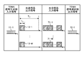
- FIG. 2 is a diagram showing an example of a signal transmitted in the optical communication system 200 according to the first embodiment.
- FIG. 2 also shows the flow of operation of the optical communication system 200 according to the first embodiment.
- the first data signal which is an input signal to the TDMA signal generation unit 11, is a continuous signal having a constant voltage amplitude.
- the TDMA signal generation unit 11 cuts a signal in a certain time domain or signal block region, packets it for transmitting the signal to each optical transmitter 13, and increases the transmission speed.
- FIG. 2 shows a case where the time domain is divided with an emphasis on comprehensibility.
- the TDMA signal generation unit 11-1 divides the first data signal, which is an input signal, by the time domain TC .
- All the signals separated by the time domain TC are destined for an arbitrary destination, for example, the TDMA signal selection unit 72-1.
- the TDMA signal generation unit 11-1 speeds up the divided signal so as not to collide with the signal from another TDMA signal generation unit 11 in the time domain, that is, compresses the signal in the time domain.
- the signal time widths PP of the signals transmitted to the optical transmitter 13 connected to one TDMA signal generation unit 11 are all the same and at the same timing, but from the other TDMA signal generation units 11. If the signal does not collide with the signal in the optical fiber network, the signal time width may be different and the signal timing may be different.
- the optical transmitter 13 converts the packet signal of the electric signal transmitted after the transmission timing is determined by the TDMA signal generation unit 11 into the packet signal of the optical signal.
- the optical transmitter 13 outputs the packet signal of the optical signal to the optical coupler 20 to be connected.
- all the optical transmitter output signals of the optical transmitters 13-1 to 13-M are described as "1", because this represents the signal received from the TDMA signal generation unit 11-1. Therefore, the contents of the packets expressed in parallel are all different.
- the packet signal of the optical signal output from the optical transmitter 13-1 indicates a signal with a relative time of 0 msec to 0.125 msec of the input signal to the TDMA signal generation unit 11-1, and is transmitted from the optical transmitter 13-2.
- the packet signal of the output optical signal indicates a signal having a relative time of 0.125 msec to 0.25 msec of the input signal to the TDMA signal generation unit 11-1.
- the optical couplers 20-1 to 20-LM each combine the packet signals of the optical signals acquired from the K optical transmitters 13 to be connected.
- the optical couplers 20-1 to 20-LM branch the packet signal of the combined optical signal into transmission signals of N optical signals of the same information, and one optical receiver 71 included in each optical receiver 70. That is, it outputs to N optical receivers 71.
- the optical couplers 20-1 to 20-LM shall have a K input port and an N output port, respectively.
- K is an integer of 2 or more and smaller than N.
- the optical couplers 20-1 to 20-LM combine the packet signals of the acquired optical signals, demultiplex them into transmission signals of N optical signals, and transmit them to N optical receivers 71. Therefore, the transmission signal of the optical signal acquired by the optical receivers 71-1 to 71-LM connected to the TDMA signal selection unit 72-1 is also connected to each of the TDMA signal selection units 72-1 to 72-N. It is also acquired by the LM optical receivers 71.
- the transmission signal of the optical signal acquired by the optical receiver 71-1 is connected to the first optical receiver 71- (LM + 1) connected to the TDMA signal selection unit 72-2 and the TDMA signal selection unit 72-3. It is also acquired by the first optical receiver 71- (LM2 + 1) or the like.
- the transmission signal of the optical signal acquired by the optical receiver 71-M is connected to the Mth optical receiver 71- (LM + M) connected to the TDMA signal selection unit 72-2 and the TDMA signal selection unit 72-3. It is also acquired by the Mth optical receiver 71- (LM2 + M) or the like.
- the portion described as "1" in the transmission signal of the optical signal shown in the top row is the TDMA signal generation unit 11-1.
- the signals with a relative time of 0 msec to 0.125 msec are shown, and the portion described as "2" is the input signal to the TDMA signal generation unit 11-2 with a relative time of 0 msec to 0.125 msec.
- a signal is shown, and the portion described as “K” indicates a signal having a relative time of 0 msec to 0.125 msec among the input signals to the TDMA signal generation unit 11-K, and is a total signal of 1 msec. ..
- the transmission signal of the optical signal to be next to the transmission signal of the optical signal shown in the top row is TDMA.
- the signals have a relative time of 0.125 msec to 0.25 msec.
- N TDMA signal selection units 72 are transmitted from MN optical transmitters 13 connected to N TDMA signal generation units 11 via LM optical receivers 71.
- the packet signal of the optical signal it is possible to reconstruct the signal having a relative time of 0 msec to 1 msec and select the TDMA signal, that is, the selection of the second data signal which is an electric signal.
- all the packet signals are signals having the same signal time width T P , but packets having different signal time width T P may be used for each TDMA signal generation unit 11.
- the optical receivers 71-1 to 71-LM convert the acquired optical signal transmission signal into an electrical signal transmission signal.
- the transmission signal of the optical signal acquired by a certain optical receiver 71 when the transmission path loss from each optical transmitter 13 to the optical receiver 71, the output optical power of the optical transmitter 13, and the like are different, the optical signal There is a difference in optical level between the transmitted signals. This optical level difference can be absorbed without changing the photoelectric conversion gain of the optical receiver 71, that is, it can be converted into a signal having a constant voltage amplitude.
- the photoelectric conversion gain is used as the transmission signal of the optical signal. It may be necessary to change each time.
- a relative phase for example, an NRZ (Non-Return to Zero) signal is used. If so, the phases of the rising edge and the falling edge are generally different. In this case, it is necessary to optimize the state of the optical receiver 71 for each transmission signal of the optical signal in order to absorb the optical level difference, the phase difference, and the like so that signal loss does not occur. Therefore, a preamble pattern is inserted at the beginning of the packet in the transmission signal of each optical signal.
- ITU International Telecommunication Union
- XGS-PON 10 Gigabit capable Symmetric-Passive Optical Network
- the preamble length is specified to be 128.6 ns to 610.9 ns, and an appropriate preamble pattern may be inserted according to the system configuration.
- the longer the preamble length the more the optimization time required for the optical transmitter 13 and the optical receiver 71 is relaxed, but in order to maintain the desired switching capability, improvements in transmission speed, time compression rate, and the like are required.
- the TDMA signal selection unit 72 acquires an electric signal transmission signal from the connected optical receiver 71.
- the TDMA signal selection unit 72 selects a signal in the specified time slot from the transmission signal of the received electric signal based on the routing information included in the second control signal acquired from the control unit 100, and selects the selected time slot. Is output as a second data signal which is an electric signal.
- the TDMA signal selection unit 72 extracts only necessary destinations based on the routing information, and discards other signals.
- the TDMA signal selection unit 72 converts a time-intermittent extraction signal into a time-continuous signal, converts the transmission speed according to the system connected to the subsequent stage, and sends the signal.
- the TDMA signal selection unit output signal shown in FIG. 2 shows, as an example, a second data signal output from the TDMA signal selection unit 72-1.
- the control unit 100 generates control information necessary for the TDMA signal generation unit 11 and the TDMA signal selection unit 72 to perform the above-mentioned control, a reference clock for the entire optical communication system 200 to operate in synchronization, and the like. , Supply to each part.
- the control unit 100 generates, as a first control signal, a reference clock, a transmission timing signal for allocating communication resources, and routing information, and distributes them to the TDMA signal generation units 11-1 to 11-N. Further, the control unit 100 distributes the transmission timing signal, which is the communication resource allocation, and the routing information as the second control signal to the TDMA signal selection units 72-1 to 72-N.
- the control unit 100 transmits other necessary control signals such as a state transition signal of the optical transmitter 13 to each optical transmitter 13 and each optical receiver 71. May be supplied.
- FIG. 1 shows only a line for supplying control information from the control unit 100 to the TDMA signal generation unit 11 and the TDMA signal selection unit 72, but the present invention is not limited to this.
- the control unit 100 may acquire state information, for example, failure information from each configuration as necessary, and may change the packet signal allocation, destination, and the like based on the state information of each configuration.
- each of the optical communication system 200 converts the first data signal, which is an electric signal, into a packet signal of a plurality of optical signals and transmits the plurality of optical transmission devices 10-1.
- ⁇ 10-N and packet signals of a plurality of optical signals transmitted from a part of the optical transmission devices 10 among the plurality of optical transmission devices 10-1 to 10-N and transmitted from different optical transmission devices 10.
- 20-1 to 20-LM are provided, and the packet signal of the combined optical signal is branched into transmission signals of a plurality of optical signals of the same information and output.
- each of the optical communication system 200 receives one of the transmission signals of the optical signal branched by the plurality of optical couplers 20-1 to 20-LM from the plurality of optical couplers 20-1 to 20-LM.
- a plurality of optical receivers 70-1 to 70-N converted into a second data signal which is an electric signal and output, a plurality of optical transmitters 10-1 to 10-N, and a plurality of optical receivers 70-.
- a control unit 100 for controlling the operation of 1 to 70-N is provided.
- the wave number of the optical couplers 20-1 to 20-LM is smaller than the number of the plurality of optical transmitters 10-1 to 10-N.
- the optical transmission device 10 allocates communication resources based on the first control signal acquired from the control unit 100 so as not to collide with the packet signals of the optical signals transmitted from the other optical transmission devices 10, and a plurality of optical signals. Send the packet signal of.
- the optical receiver 70 converts the transmission signal of the optical signal into the transmission signal of the electric signal, and selects a signal portion designated from the transmission signal of the electric signal based on the second control signal acquired from the control unit 100. , Is output as a second data signal.
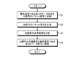
- FIG. 3 is a flowchart showing the operation of the optical communication system 200 according to the first embodiment.
- Each of the optical transmission devices 10-1 to 10-N converts the first data signal, which is an electric signal, into a packet signal of an optical signal and transmits it based on the control of the control unit 100 (step S1).
- each optical transmission device 10 allocates communication resources based on the first control signal acquired from the control unit 100 so as not to collide with the packet signal of the optical signal transmitted from the other optical transmission device 10.
- the optical couplers 20-1 to 20-LM combine the packet signals of a plurality of optical signals received from the optical transmission devices 10-1 to 10-N (step S2), and the transmitted signals of the combined optical signals are the same.
- the information is branched into transmission signals of a plurality of optical signals and output (step S3).
- Each of the optical receivers 70-1 to 70-N receives a transmission signal of an optical signal branched by the optical couplers 20-1 to 20-LM based on the control of the control unit 100, and is an electric signal. It is converted into the data signal of No. 2 and output (step S4).
- each optical receiving device 70 converts the transmission signal of the optical signal into the transmission signal of the electric signal, and based on the second control signal acquired from the control unit 100, the signal designated from the transmission signal of the electric signal. The part is selected and output as a second data signal.
- the control unit 100 controls the operations of the optical transmitting devices 10-1 to 10-N and the optical receiving devices 70-1 to 70-N.
- the optical transmission devices 10-1 to 10-N do not collide with the packet signal of the optical signal transmitted from the other optical transmission device 10 based on the first control signal. Allocate a time slot so that a packet signal of an optical signal is transmitted. Further, the optical receivers 70-1 to 70-N select a signal in the designated time slot from the transmission signal of the electric signal based on the second control signal, and output the signal as the second data signal.
- the optical transmitter 13 and the optical receiver 71 are photoelectric conversion circuits.
- the optical coupler 20 is a power splitter as described above.
- the TDMA signal generation unit 11, the TDMA signal selection unit 72, and the control unit 100 are realized by a processing circuit.
- the processing circuit may be a processor and memory for executing a program stored in the memory, or may be dedicated hardware.
- the processing circuit is also called a control circuit.
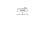
- FIG. 4 is a diagram showing a configuration example of a processing circuit 300 in the case where the processing circuit included in the optical communication system 200 according to the first embodiment is realized by a processor and a memory.
- the processing circuit 300 shown in FIG. 4 is a control circuit and includes a processor 301 and a memory 302.
- each function of the processing circuit 300 is realized by software, firmware, or a combination of software and firmware.
- the software or firmware is written as a program and stored in memory 302.
- each function is realized by the processor 301 reading and executing the program stored in the memory 302. That is, the processing circuit 300 includes a memory 302 for storing a program in which the processing of the optical communication system 200 is eventually executed. It can be said that this program is a program for causing the optical communication system 200 to execute each function realized by the processing circuit 300.
- This program may be provided by a storage medium in which the program is stored, or may be provided by other means such as a communication medium.
- the above program prevents the control unit 100 from colliding with the optical transmission device 10 from the packet signal of the optical signal transmitted from the other optical transmission device 10 based on the first control signal acquired from the control unit 100.
- Communication resources are allocated, packet signals of a plurality of optical signals are transmitted, the optical receiving device 70 converts the transmitted signal of the optical signal into the transmitted signal of the electric signal, and is based on the second control signal acquired from the control unit 100. Therefore, it can be said that it is a program that selects a designated signal portion from the transmission signal of the electric signal and outputs it as a second data signal.
- the processor 301 is, for example, a CPU (Central Processing Unit), a processing device, an arithmetic unit, a microprocessor, a microcomputer, a DSP (Digital Signal Processor), or the like.
- the memory 302 is, for example, non-volatile or volatile such as RAM (Random Access Memory), ROM (Read Only Memory), flash memory, EPROM (Erasable Programmable ROM), and EPROM (registered trademark) (Electrically EPROM). This includes semiconductor memory, magnetic discs, flexible discs, optical discs, compact discs, mini discs, DVDs (Digital Versatile Disc), and the like.
- FIG. 5 is a diagram showing an example of a processing circuit 303 in the case where the processing circuit included in the optical communication system 200 according to the first embodiment is configured by dedicated hardware.
- the processing circuit 303 shown in FIG. 5 is, for example, a single circuit, a composite circuit, a programmed processor, a parallel programmed processor, an ASIC (Application Specific Integrated Circuit), an FPGA (Field Programmable Gate Array), or a combination thereof. The thing is applicable.
- the processing circuit a part may be realized by dedicated hardware and a part may be realized by software or firmware.
- the processing circuit can realize each of the above-mentioned functions by the dedicated hardware, software, firmware, or a combination thereof.
- the optical communication system 200 uses a TDMA method to control the transmission timing of the TDMA signal generation unit 11 of each optical transmission device 10, thereby performing an optical switch in the optical region. Since the matrix switch connection can be configured only by the passive component of the optical coupler 20 without using the above, it is possible to improve the reliability. Further, in the optical communication system 200, by limiting the combined wave number of the optical coupler 20, the number of packets combined around the optical coupler 20 can be limited, and the line efficiency can be improved.
- the optical switch for example, a Mach-Zehnder interferometer is exemplified, but the power consumption, cost, size, and weight per switch port are larger than those of an electric switch configured by ASIC, and the route switching information is displayed.
- the switching time required from confirmation to switching is as long as several tens of us.
- the optical communication system 200 does not use an optical switch, it is possible to realize low power consumption, space saving, weight reduction, cost reduction, and shortening of route switching time.
- each optical receiver 70 includes the same number of optical receivers 71 as the optical coupler 20.
- each optical transmitter 10 includes the same number of optical transmitters 13 as the optical coupler 20 will be described.
- FIG. 6 is a diagram showing a configuration example of the optical communication system 200 according to the second embodiment.
- the optical communication system 200 shown in FIG. 6 is a system having N input ports and N output ports (not shown), and switching between the input N port and the output N port by the TDMA method.
- the optical communication system 200 includes TDMA signal generators 11-1 to 11-N, optical transmitters 13-1 to 13-LMN, optical couplers 20-1 to 20-LM, and optical receivers 71-1 to 71.
- -MN, TDMA signal selection units 72-1 to 72-N, and control unit 100 are provided.
- L, M, and N are integers of 2 or more.
- K which will be described later, is an integer of 2 or more and smaller than N.
- the optical transmission device 10-1 is composed of the TDMA signal generation unit 11-1 and the optical transmitters 13-1 to 13-LM, and the TDMA signal generation unit 11-2 and the optical transmitter 13- (LM + 1). ) -13-LM2 constitutes the optical transmitter 10-2, ..., TDMA signal generator 11-N and optical transmitter 13- (LM (N-1) + 1) -13-LMN configure the optical transmitter 10-. N is configured.
- the optical receiver 70-1 is configured by the optical receivers 71-1 to 71-M and the TDMA signal selection unit 72-1, and the optical receivers 71- (M + 1) to 71-M2 and the TDMA signal selection unit 72-
- the optical receiver 70-2 is configured by 2, ..., the optical receiver 71- (M (N-1) +1) to 71-MN, and the optical receiver 70-N are configured by the TDMA signal selection unit 72-N.
- the optical couplers 20-1 to 20-LM are, for example, power splitters.
- the optical transmission devices 10-1 to 10-N are not distinguished, they are referred to as an optical transmission device 10, and when the TDMA signal generation units 11-1 to 11-N are not distinguished, they are referred to as a TDMA signal generation unit 11.
- the optical transmitters 13-1 to 13-LMN are not distinguished, they may be referred to as an optical transmitter 13.
- the optical couplers 20-1 to 20-LM are not distinguished, they may be referred to as an optical coupler 20.
- the optical receivers 70-1 to 70-N are not distinguished, the optical receiver 70 is referred to, and when the optical receivers 71-1 to 71-MN are not distinguished, the optical receiver 71 is referred to as a TDMA signal selection unit.
- 72-1 to 72-N are not distinguished, it may be referred to as a TDMA signal selection unit 72.
- each of the optical couplers 20-1 to 20-LM is a packet signal of an optical signal transmitted from one optical transmitter 13 provided in each optical transmitter 10, that is, N optical transmitters 13. To combine waves.
- the optical couplers 20-1 to 20-LM branch the packet signal of the combined optical signal into transmission signals of K optical signals of the same information and output them to the connected optical receivers 71. ..
- the optical couplers 20-1 to 20-LM shall have an N input port and a K output port, respectively.
- the number of optical transmitters 13 connected to each TDMA signal generation unit 11 increases to LM as compared with the first embodiment, while the number of optical transmitters 13 connected to each TDMA signal selection unit 72 is increased.
- the number of optical receivers 71 is reduced to M.
- the total number of the number of optical transmitters 13 and the total number of optical receivers 71 is the same in the first embodiment and the second embodiment.
- the number of merging signals and the number of demultiplexing signals in the optical couplers 20-1 to 20-LM differ between the first embodiment and the second embodiment, they are demultiplexed with the number of merging signals.
- the total number including the number of signals is the same in the first embodiment and the second embodiment.
- FIG. 7 is a diagram showing an example of a signal transmitted in the optical communication system 200 according to the second embodiment.
- FIG. 7 also shows the flow of operation of the optical communication system 200 according to the second embodiment.
- the TDMA signal generation unit 11 divides the first data, which is an input signal, in time and changes it into a packet signal of an electric signal that is intermittent in time.
- the number of output ports of the optical couplers 20-1 to 20-LM is limited. Therefore, for example, the TDMA signal generation unit 11-1 replicates the packet signal of the same electric signal to the L optical transmitters 13 every M of the connected optical transmitters 13-1 to 13-LM. And send.
- the TDMA signal generation unit input signal shown in FIG. 7 shows, as an example, a first data signal which is an input signal to the TDMA signal generation unit 11-1.
- the optical transmitter 13 converts the packet signal of the electric signal transmitted after the transmission timing is determined by the TDMA signal generation unit 11 into the packet signal of the optical signal.
- the optical transmitter 13 outputs the packet signal of the optical signal to the optical coupler 20 to be connected.
- the packet signal of the optical signal output from M + 1) is the same signal.
- the packet signals of the optical signals output from the optical transmitters 13-M, 13-2M, 13-3M, ..., 13-LM connected to the TDMA signal generation unit 11-1 are the same signal. Become.
- each of the optical couplers 20-1 to 20-LM receives a packet signal of an optical signal transmitted from one optical transmitter 13 included in each optical transmitter 10, that is, N optical transmitters 13. Combine waves.
- the optical couplers 20-1 to 20-LM branch the packet signal of the combined optical signal into transmission signals of K optical signals of the same information and output them to the connected optical receivers 71. ..
- the optical receiver input signal of FIG. 7 specifically shows a transmission signal of an optical signal acquired by the optical receivers 71-1 and 71-M.
- the TDMA signal selection unit 72 transmits an electric signal received from the connected optical receiver 71 based on the routing information included in the second control signal acquired from the control unit 100.
- the signal of the designated time slot is selected from the signal, and the signal of the selected time slot is output as the second data signal which is an electric signal.
- the TDMA signal selection unit 72 extracts only necessary destinations based on the routing information, and discards other signals.
- the TDMA signal selection unit 72 converts a time-intermittent extraction signal into a time-continuous signal, converts the transmission speed according to the system connected to the subsequent stage, and sends the signal.
- the TDMA signal selection unit output signal shown in FIG. 7 shows, as an example, a second data signal output from the TDMA signal selection unit 72-1.
- each of the optical communication system 200 converts the first data signal, which is an electric signal, into a packet signal of a plurality of optical signals and transmits the plurality of optical transmission devices 10-1.
- ⁇ 10-N each of which is transmitted from a plurality of optical transmission devices 10-1 to 10-N, and the packet signals of a plurality of optical signals transmitted from different optical transmission devices 10 are combined and combined.
- It includes a plurality of optical couplers 20-1 to 20-LM for branching and outputting a packet signal of a signal into transmission signals of a plurality of optical signals of the same information.
- each of the optical communication system 200 receives one of the transmission signals of the optical signal branched by the optical coupler 20 from some of the optical couplers 20 among the plurality of optical couplers 20-1 to 20-LM.
- a plurality of optical receivers 70-1 to 70-N converted into a second data signal which is an electric signal and output, a plurality of optical transmitters 10-1 to 10-N, and a plurality of optical receivers 70-.
- a control unit 100 for controlling the operation of 1 to 70-N is provided.
- the number of branches of the optical couplers 20-1 to 20-LM is smaller than the number of the plurality of optical receivers 70-1 to 70-N.
- the optical transmission device 10 duplicates the first data signal based on the first control signal acquired from the control unit 100, and does not collide with the packet signal of the optical signal transmitted from another optical transmission device 10 for each destination. By allocating communication resources so as to transmit packet signals of multiple optical signals.
- the optical receiver 70 converts the transmission signal of the optical signal into the transmission signal of the electric signal, and selects a signal portion designated from the transmission signal of the electric signal based on the second control signal acquired from the control unit 100. , Is output as a second data signal.
- the optical communication system 200 uses a TDMA method to control the transmission timing of the TDMA signal generation unit 11 of each optical transmission device 10, thereby performing an optical switch in the optical region. Since the matrix switch connection can be configured only by the passive component of the optical coupler 20 without using the above, it is possible to improve the reliability. In the present embodiment, since each optical coupler 20 combines the signals transmitted from all the TDMA signal generation units 11, the number of TDMA signal generation units 11 for transmitting the signals is small, that is, the signals are sparse. In this case, the optical communication system 200 can improve the line efficiency as compared with the first embodiment.
- Embodiment 3 In the first embodiment and the second embodiment, the total number of the optical transmitters 13 and the optical receivers 71 is the same. In the third embodiment, a case where the total number of the number of the optical transmitters 13 and the number of the optical receivers 71 is reduced as compared with the case of the first embodiment and the second embodiment will be described.
- FIG. 8 is a diagram showing a configuration example of the optical communication system 200 according to the third embodiment.
- the optical communication system 200 shown in FIG. 8 is a system having N input ports and N output ports (not shown), and switching between the input N port and the output N port by the TDMA method.
- the optical communication system 200 includes TDMA signal generation units 11-1 to 11-N, transmission switch units 12-1 to 12-N, optical transmitters 13-1 to 13-MN, and optical couplers 20-1 to 20.
- -LM, optical receivers 71-1 to 71-MN, TDMA signal selection units 72-1 to 72-N, and control unit 100 are provided.
- L, M, and N are integers of 2 or more.
- the optical transmission device 10-1 is configured by the TDMA signal generation unit 11-1, the transmission switch unit 12-1, and the optical transmitters 13-1 to 13-M, and the TDMA signal generation unit 11-2.
- Transmission switch unit 12-2, and optical transmitters 13- (M + 1) to 13-M2 constitute the optical transmission device 10-2, ..., TDMA signal generation unit 11-N, transmission switch unit 12-N, and
- the optical transmitters 10-N are configured by the optical transmitters 13- (M (N-1) +1) to 13-MN.
- the optical receiver 70-1 is configured by the optical receivers 71-1 to 71-M and the TDMA signal selection unit 72-1, and the optical receivers 71- (M + 1) to 71-M2 and the TDMA signal selection unit 72-
- the optical receiver 70-2 is configured by 2, ..., the optical receiver 71- (M (N-1) +1) to 71-MN, and the optical receiver 70-N are configured by the TDMA signal selection unit 72-N.
- the optical couplers 20-1 to 20-LM are, for example, power splitters.
- optical transmission devices 10-1 to 10-N when the optical transmission devices 10-1 to 10-N are not distinguished, they are referred to as an optical transmission device 10, and when the TDMA signal generation units 11-1 to 11-N are not distinguished, they are referred to as a TDMA signal generation unit 11.
- the transmission switch units 12-1 to 12-N when the transmission switch units 12-1 to 12-N are not distinguished, the transmission switch unit 12 may be referred to, and when the optical transmitters 13-1 to 13-MN are not distinguished, the optical transmitter unit 13 may be referred to.
- optical couplers 20-1 to 20-LM when the optical couplers 20-1 to 20-LM are not distinguished, they may be referred to as an optical coupler 20.
- the optical receiver 70 is referred to, and when the optical receivers 71-1 to 71-MN are not distinguished, the optical receiver 71 is referred to as a TDMA signal selection unit.
- the optical receiver 71 is referred to as a TDMA signal selection unit.
- 72-1 to 72-N it may be referred to as a TDMA signal selection unit 72.
- the optical couplers 20-1 to 20-LM each combine the packet signals of the optical signals transmitted from the K optical transmitters 13.
- the optical couplers 20-1 to 20-LM branch the packet signal of the combined optical signal into transmission signals of J optical signals of the same information and output them to the connected optical receivers 71. ..
- the optical couplers 20-1 to 20-LM shall have a K input port and a J output port, respectively.
- K and J are integers greater than or equal to 2 and less than N. Note that K and J may be the same integer or different integers depending on the configuration of the optical communication system 200.
- the number of optical transmitters 13 connected to each TDMA signal generation unit 11 and the number of optical receivers 71 connected to each TDMA signal selection unit 72 are both M.
- the total number of the number of optical transmitters 13 and the total number of optical receivers 71 can be reduced as compared with the case of the first embodiment and the second embodiment.
- the number of the combined signal or the larger number of the demultiplexing signals in the optical couplers 20-1 to 20-LM is larger than that in the first and second embodiments. Can also be reduced, so the loss budget can be reduced.
- FIG. 9 is a diagram showing an example of a signal transmitted in the optical communication system 200 according to the third embodiment.
- FIG. 9 also shows the flow of operation of the optical communication system 200 according to the third embodiment.
- the TDMA signal generation unit 11 divides the first data, which is an input signal, in time and changes it into a packet signal of an electric signal that is intermittent in time.
- the TDMA signal generation unit input signal shown in FIG. 9 shows, as an example, a first data signal which is an input signal to the TDMA signal generation unit 11-1.
- the number of input ports and the number of output ports of each optical coupler 20 are limited, and the TDMA signal selection unit 72 connected via the optical receiver 71 differs depending on the optical coupler 20.
- the transmission switch unit 12 switches so as to separate the optical transmitter 13 for transmitting the packet signal of each electric signal generated by the TDMA signal generation unit 11 for each destination TDMA signal selection unit 72.
- the TDMA signal selection unit 72-1 transmits the destination signal to the optical transmitter 13-1
- the TDMA signal selection unit 72-N optically transmits the destination signal. It is transmitted to the vessel 13-M.
- the optical transmitter 10 switches the signal to be transmitted for each optical transmitter 13 in advance by the transmission switch unit 12.
- the optical communication system 200 can switch from a certain input port to a desired output port even when the number of input / output ports of the optical coupler 20 is limited.
- the optical transmitter output signal is an output signal from the optical transmitter 13-1 and the optical transmitter 13-M that have acquired a signal from the TDMA signal generation unit 11-1 by switching by the transmission switch unit 12-1. Shows.
- the signal time width T P of the packet signal of the optical signal transmitted from the optical transmitters 13-1 and 13-M is the same, but the signal time width T P is different for each destination. Therefore, the signal time width T P of the packet signal of the optical signal transmitted from each optical transmitter 13 may be different.
- FIG. 9 shows an example of a transmission signal of an optical signal received by the optical receiver 71-1 connected to the TDMA signal selection unit 72-1 in the optical receiver input signal.
- the packet signal of the optical signal from the optical coupler 20-1 to the optical transmitters 13-1, 13- (M + 1), ..., 13-((K-1) M + 1) is combined. Acquires the transmission signal of the optical signal.
- the packet signal of the optical signal from the optical transmitter 13-1 is based on the packet signal of the electric signal transmitted from the TDMA signal generation unit 11-1, and is a packet of the optical signal from the optical transmitter 13- (M + 1).
- the signal is based on the packet signal of the electric signal transmitted from the TDMA signal generation unit 11-2, and ..., the packet signal of the optical signal from the optical transmitter 13-((K-1) M + 1) is the TDMA signal generation. It is based on the packet signal of the electric signal transmitted from the unit 11-K.
- the optical transmission device 10 connected to the optical coupler 20-1 is an optical transmission device 10-1 to 10-K is shown, but it is an example and is not limited thereto.
- the optical transmission device connected to the optical coupler 20-1 may be an optical transmission device 10-1, 10-2 to 10- (K + 1).
- the packet signal of the optical signal is input from all of the K optical transmitters 13 to the optical coupler 20 is shown, but the light is only from a limited optical transmitter 13.
- the packet signal of the signal is input to the optical coupler 20, the packet signal of each optical signal may be spaced apart, or the signal time width T P may be lengthened.
- the optical receiver 71 converts the acquired optical signal transmission signal into an electrical signal transmission signal and outputs it to the TDMA signal selection unit 72.
- the TDMA signal selection unit 72 transmits an electric signal received from the connected optical receiver 71 based on the routing information included in the second control signal acquired from the control unit 100.
- the signal of the designated time slot is selected from the signal, and the signal of the selected time slot is output as the second data signal which is an electric signal.
- the TDMA signal selection unit 72 extracts only necessary destinations based on the routing information, and discards other signals.
- the TDMA signal selection unit 72 converts a time-intermittent extraction signal into a time-continuous signal, converts the transmission speed according to the system connected to the subsequent stage, and sends the signal.
- the TDMA signal selection unit output signal shown in FIG. 9 shows, as an example, a second data signal output from the TDMA signal selection unit 72-1.
- each of the optical communication system 200 converts the first data signal, which is an electric signal, into a packet signal of a plurality of optical signals and transmits the plurality of optical transmission devices 10-1.
- ⁇ 10-N and packet signals of a plurality of optical signals transmitted from a part of the optical transmission devices 10 among the plurality of optical transmission devices 10-1 to 10-N and transmitted from different optical transmission devices 10.
- 20-1 to 20-LM are provided, and the packet signal of the combined optical signal is branched into transmission signals of a plurality of optical signals of the same information and output.
- each of the optical communication system 200 receives one of the transmission signals of the optical signal branched by the optical coupler 20 from some of the optical couplers 20 among the plurality of optical couplers 20-1 to 20-LM.
- a plurality of optical receivers 70-1 to 70-N converted into a second data signal which is an electric signal and output, a plurality of optical transmitters 10-1 to 10-N, and a plurality of optical receivers 70-.
- a control unit 100 for controlling the operation of 1 to 70-N is provided.
- the wave number of the optical couplers 20-1 to 20-LM is less than the number of the plurality of optical transmitters 10-1 to 10-N, and the number of branches of the optical couplers 20-1 to 20-LM is the number of branches of the plurality of optical receivers 70. Less than the number of -1 to 70-N.
- the optical transmission device 10 switches to optical couplers 20 having different destinations for each destination based on the first control signal acquired from the control unit 100, and the packet signal of the optical signal transmitted from the other optical transmission device 10 for each destination. Allocate communication resources so as not to collide with, and transmit the packet signal of the optical signal.
- the optical receiver 70 converts the transmission signal of the optical signal into the transmission signal of the electric signal, and selects a signal portion designated from the transmission signal of the electric signal based on the second control signal acquired from the control unit 100. , Is output as a second data signal.
- the transmission switch unit 12 is realized by a processing circuit.
- the processing circuit may be a processor and memory for executing a program stored in the memory, or may be dedicated hardware.
- the optical communication system 200 uses a TDMA method to control the transmission timing of the TDMA signal generation unit 11 of each optical transmission device 10, thereby performing an optical switch in the optical region. Since the matrix switch connection can be configured only by the passive component of the optical coupler 20 without using the above, it is possible to improve the reliability. Further, the optical communication system 200 can suppress the loss of the optical coupler 20 by limiting the wave number and the branch number of the optical coupler 20. In the present embodiment, the loss budget can be reduced as compared with the first embodiment and the second embodiment, and the total number of the number of optical transmitters 13 and the total number of optical receivers 71 can be reduced. Can be done.
- Embodiment 4 a case where the optical communication system 200 includes a TDMA switch for switching an electric signal will be described.
- FIG. 10 is a diagram showing a configuration example of the optical communication system 200 according to the fourth embodiment.
- the optical communication system 200 shown in FIG. 10 is a system having N input ports and N output ports (not shown), and switching between the input N port and the output N port by the TDMA method.
- the optical communication system 200 includes TDMA signal generators 11-1 to 11-N, optical transmitters 13-1 to 13-MN, optical couplers 20-1 to 20-LM, and optical receivers 30-1 to 30.
- TDMA switches 40-1 to 40-L optical transmitters 50-1 to 50-LJM, optical couplers 60-1 to 60-MN, optical receivers 71-1 to 71-MN, and A TDMA signal selection unit 72-1 to 72-N and a control unit 100 are provided.
- the optical transmitter is referred to as Tx
- the optical receiver is referred to as Rx.
- J, L, M, and N are integers of 2 or more.
- the optical transmission device 10-1 is composed of the TDMA signal generation unit 11-1 and the optical transmitters 13-1 to 13-M, and the TDMA signal generation unit 11-2 and the optical transmitter 13- (M + 1). ) ⁇ 13-M2 constitutes the optical transmitter 10-2, ..., The optical transmitter 10- by the TDMA signal generator 11-N and the optical transmitter 13- (M (N-1) +1) to 13-MN. N is configured.
- the optical receiver 70-1 is configured by the optical receivers 71-1 to 71-M and the TDMA signal selection unit 72-1, and the optical receivers 71- (M + 1) to 71-M2 and the TDMA signal selection unit 72-
- the optical receiver 70-2 is configured by 2, ..., the optical receiver 71- (M (N-1) +1) to 71-MN, and the optical receiver 70-N are configured by the TDMA signal selection unit 72-N.
- the optical couplers 20-1 to 20-LM and the optical couplers 60-1 to 60-MN are, for example, power splitters.
- optical transmission devices 10-1 to 10-N when they are referred to as an optical transmission device 10, and when the TDMA signal generation units 11-1 to 11-N are not distinguished, they are referred to as a TDMA signal generation unit 11.
- the optical transmitters 13-1 to 13-MN When the optical transmitters 13-1 to 13-MN are not distinguished, they may be referred to as an optical transmitter 13.
- optical couplers 20-1 to 20-LM When the optical couplers 20-1 to 20-LM are not distinguished, they are referred to as optical couplers 20, and when the optical receivers 30-1 to 30-LM are not distinguished, they are referred to as optical receivers 30 and TDMA switches 40-1 to 40-1 to When 40-L is not distinguished, it is called TDMA switch 40, when optical transmitters 50-1 to 50-LJM are not distinguished, it is called optical transmitter 50, and when optical couplers 60-1 to 60-MN are not distinguished, it is called. It may be referred to as an optical coupler 60.
- the optical receiver 70 When the optical receivers 70-1 to 70-N are not distinguished, the optical receiver 70 is referred to, and when the optical receivers 71-1 to 71-MN are not distinguished, the optical receiver 71 is referred to as a TDMA signal selection unit. When 72-1 to 72-N are not distinguished, it may be referred to as a TDMA signal selection unit 72.
- the optical transmitter 10 is referred to as a first optical transmitter
- the optical coupler 20 is referred to as a first optical coupler
- the optical receiver 30 is referred to as a first optical receiver
- the optical transmitter 50 is referred to as a second optical transmitter.
- the optical transmitter 60 may be referred to as a second optical coupler
- the optical receiver 70 may be referred to as a second optical receiver.
- the optical communication system 200 includes TDMA switches 40-1 to 40-L that perform optical-electrical-optical conversion and switch electric signals in order to carry out NxN switching.
- the optical communication system 200 can reduce the combined wave number of the optical coupler 20 and the demultiplexing number of the optical coupler 60 per stage as compared with the cases of the first to third embodiments. The loss budget can be reduced. Further, since the optical communication system 200 can extend the signal time width TP per packet, the transmission speed required for the optical transmitters 13 and 50 and the optical receivers 30 and 71 can also be reduced.
- FIG. 11 is a diagram showing an example of a signal transmitted in the optical communication system 200 according to the fourth embodiment.
- FIG. 11 also shows the flow of operation of the optical communication system 200 according to the fourth embodiment.
- the TDMA signal generation unit 11 divides the first data, which is an input signal, into a packet signal of an electric signal having a time-intermittent signal time width T P1 . ..
- the TDMA signal generation unit input signal shown in FIG. 11 shows, as an example, a first data signal which is an input signal to the TDMA signal generation unit 11-1.
- the optical transmitter 13 converts the packet signal of the electric signal having the signal time width T P1 generated by the TDMA signal generation unit 11 into the packet signal of the optical signal. Send.
- the optical couplers 20-1 to 20-LM shall have a K input port and one output port, respectively.
- the optical couplers 20-1 to 20-LM combine packet signals of a maximum of K optical signals, and transmit the transmitted signal of the combined optical signals to the optical receiver 30.
- FIG. 11 shows an input signal from the optical coupler 20-1 to the optical receiver 30-1 and an input signal from the optical coupler 20-M to the optical receiver 30-M as the optical receiver 30 input signal. ..
- the optical receivers 30-1, 30-M receive the transmission signal of the optical signal to which the packet signals of K optical signals are combined.
- the optical receiver 30 converts the transmitted signal of the received optical signal into a data signal which is an electric signal and transmits it to the TDMA switch 40.
- K is an integer of 2 or more and smaller than N.
- the TDMA switches 40-1 to 40-L switch the data signal of the electric signal acquired from the optical receiver 30 for each destination and transmit it to the optical transmitter 50.
- the TDMA switch 40-1 finally transmits the signal generated by the TDMA signal generation unit 11-1 to the TDMA signal selection unit 72-1, so that the data signal acquired from the optical receiver 30-1 is obtained. Is shown as an example of switching to the optical transmitter 50-1.
- the TDMA switch 40-1 transmits only the packet signal 1 among the data signals of the electric signal acquired from the optical receiver 30-1, that is, the packet signals 1 to K of the electric signal, to the optical transmitters 50-1 to 50. -Output to M.
- the TDMA switch 40-1 When the TDMA switch 40-1 finally transmits the same signal generated by the TDMA signal generation unit 11-1 to the TDMA signal selection unit 72-2, the TDMA switch 40-1 sends only the packet signal 1 to the optical transmitter 50. -(M + 1) to 50-2M is output.
- the optical transmitter 50 converts the data signal of the electric signal acquired from the TDMA switch 40 into the packet signal of the optical signal and outputs it to the optical coupler 60.
- the optical transmitter 50 output signal shown in FIG. 11 shows the output signal from the optical transmitters 50-1, 50-M.
- the optical couplers 60-1 to 60-MN shall have an L input port and one output port, respectively.
- the optical couplers 60-1 to 60-MN combine packets of a maximum of L optical signals and transmit the combined optical signals to the optical receiver 71.
- FIG. 11 shows an input signal from the optical coupler 60-1 to the optical receiver 71-1 and an input signal from the optical coupler 60-M to the optical receiver 71-M as the optical receiver 71 input signal. ..
- the optical receivers 71-1 and 71-M receive the transmission signal of the optical signal to which the packet signals of the L optical signals are combined.
- the optical receiver 71 converts the acquired optical signal transmission signal into an electrical signal transmission signal and outputs it to the TDMA signal selection unit 72.
- the TDMA signal selection unit 72 transmits an electric signal received from the connected optical receiver 71 based on the routing information included in the second control signal acquired from the control unit 100.
- the signal of the designated time slot is selected from the signal, and the signal of the selected time slot is output as the second data signal which is an electric signal.
- the TDMA signal selection unit 72 extracts only necessary destinations based on the routing information, and discards other signals.
- the TDMA signal selection unit 72 converts a time-intermittent extraction signal into a time-continuous signal, converts the transmission speed according to the system connected to the subsequent stage, and sends the signal.
- the TDMA signal selection unit output signal shown in FIG. 11 shows, as an example, a second data signal output from the TDMA signal selection unit 72-1.
- each of the optical communication system 200 converts the first data signal, which is an electric signal, into the packet signals of the plurality of first optical signals, and transmits the plurality of first data signals.
- Optical transmission devices 10-1 to 10-N which are optical transmission devices, and each of the optical transmission devices 10-1 to 10-N are transmitted from some of the optical transmission devices 10 and transmitted from different optical transmission devices 10.
- optical couplers 20-1 to 20-LM which are a plurality of first optical couplers, which combine the packet signals of the plurality of first optical signals and output the transmission signal of the combined first optical signal.
- the optical communication system 200 is a plurality of first optical receivers, each of which receives a transmission signal of a first optical signal from the optical coupler 20, converts it into a second data signal which is an electric signal, and outputs the signal.
- the optical receivers 30-1 to 30-LM and each of the plurality of optical receivers 30-1 to 30-LM receive a second data signal from some of the optical receivers 30 among the plurality of optical receivers 30-1 to 30-LM, and are used for each destination. It includes TDMA switches 40-1 to 40-L, which are a plurality of switches to be switched.
- the optical communication system 200 receives a second data signal from one of the plurality of TDMA switches 40-1 to 40-L, and converts the second data signal into a packet signal of the second optical signal.
- Optical transmitters 50-1 to 50-LJM which are a plurality of second optical transmitters that convert and transmit, and some optical transmitters of the plurality of optical transmitters 50-1 to 50-LJM, respectively. It combines the packet signals of a plurality of second optical signals transmitted from the optical transmitter 50 transmitted from the 50 and connected to different TDMA switches 40, and outputs the transmitted signal of the combined second optical signal.
- the optical communication system 200 receives a transmission signal of a second optical signal from a part of the optical couplers 60 among the plurality of optical couplers 60-1 to 60-MN, and is an electric signal.
- Optical receivers 70-1 to 70-N which are a plurality of second optical receivers that are converted into data signals and output, a plurality of optical transmitters 10-1 to 10-N, and a plurality of optical receivers 70-N.
- a control unit 100 for controlling the operation of 1 to 70-N is provided.
- the wave number of the optical coupler 20 is less than the number of optical transmitters 10, and the wave number of the optical coupler 60 is smaller than the number of optical transmitters 50.
- the optical transmission device 10 Based on the first control signal acquired from the control unit 100, the optical transmission device 10 allocates communication resources so as not to collide with the packet signal of the first optical signal transmitted from the other optical transmission device 10, and a plurality of communication resources are allocated.
- the packet signal of the first optical signal of is transmitted.
- the optical receiver 70 converts the transmission signal of the second optical signal into the transmission signal of the electric signal, and based on the second control signal acquired from the control unit 100, the signal portion designated from the transmission signal of the electric signal. Is selected and output as a third data signal.
- the hardware configuration of the optical communication system 200 will be described.
- the optical receiver 30 and the optical transmitter 50 are photoelectric conversion circuits.
- the optical coupler 60 is a power splitter as described above.
- the TDMA switch 40 is realized by a processing circuit.
- the processing circuit may be a processor and memory for executing a program stored in the memory, or may be dedicated hardware.
- the optical communication system 200 uses a TDMA method to control the transmission timing of the TDMA signal generation unit 11 of each optical transmission device 10, thereby performing an optical switch in the optical region. Since the matrix switch connection can be configured only by the passive component of the optical coupler 20 without using the above, it is possible to improve the reliability. Further, the optical communication system 200 can suppress the loss of the optical couplers 20 and 60 by limiting the number of branches of the optical coupler 20 and the number of combined waves of the optical coupler 60. In the present embodiment, the loss budget can be further reduced as compared with the first to third embodiments, depending on how the number of combined branches is taken.
- the configuration shown in the above embodiments is an example, and can be combined with another known technique, can be combined with each other, and does not deviate from the gist. It is also possible to omit or change a part of the configuration.
- 10-1 to 10-N optical transmitter 11-1 to 11-N TDMA signal generator, 12-1 to 12-N transmission switch, 13-1 to 13-LMN, 50-1 to 50-LJM optical Transmitter, 20-1 to 20-LM, 60-1 to 60-MN optical coupler, 30-1 to 30-LM, 71-1 to 71-LMN optical receiver, 40-1 to 40-L TDMA switch, 70-1 to 70-N optical receiver, 72-1 to 72-N TDMA signal selection unit, 100 control unit, 200 optical communication system.
Landscapes
- Engineering & Computer Science (AREA)
- Computer Networks & Wireless Communication (AREA)
- Signal Processing (AREA)
- Physics & Mathematics (AREA)
- Electromagnetism (AREA)
- Optical Communication System (AREA)
Abstract
光通信システム(200)は、電気信号である第1のデータ信号を複数の光信号のパケット信号に変換して送信する光送信装置(10-1~10-N)と、複数の光信号のパケット信号を合波し、複数の光信号の送信信号に分岐して出力する光カプラ(20-1~20-LM)と、光信号の送信信号を受信し、電気信号である第2のデータ信号に変換して出力する光受信装置(70-1~70-N)と、光送信装置(10-1~10-N)および光受信装置(70-1~70-N)の動作を制御する制御部(100)と、を備え、光送信装置(10-1~10-N)は、他の光送信装置から送信される光信号のパケット信号に衝突しないように通信リソースを割り当て、複数の光信号のパケット信号を送信し、光受信装置(70-1~70-N)は、光信号の送信信号を電気信号の送信信号に変換し、指定された信号部分を選択し、第2のデータ信号として出力する。
Description
本開示は、光領域で信号を伝送する光通信システム、制御回路、記憶媒体および光通信方法に関する。
従来、光スイッチ装置として、特許文献1に記載されているように、M個の固定波長光源を有するN個の波長群発生器、M個の分岐/選択部、およびMN個の可変フィルタから構成されるものがある。特許文献1に記載の光スイッチ装置は、MN個の入力ポートから入力されたデータに対して、分岐/選択部でM通りの経路選択を行い、可変フィルタでN通りの波長選択を行うことによって、所望の出力ポートに経路切り替えを行ってデータを出力することができる。特許文献1に記載の光スイッチ装置の構成は、MEMS(Micro Electro Mechanical Systems)などを使用したMNxMN規模の空間マトリクススイッチと比較して、より小規模のハードウェアで光スイッチ装置を実現できる利点がある。
特許文献1に記載の光スイッチ装置が備える分岐/選択部は、DC(Delivery and Coupling)スイッチ、またはマルチキャストスイッチによって実現され、1×Mの光カプラ、およびM×1の光スイッチで構成される。しかしながら、光スイッチは、アクティブ部品のため、光カプラなどのパッシブ部品と比較して、故障率が高くなりシステム全体の信頼性が低下する、という問題があった。また、光スイッチ装置は、スイッチ規模が大きくなると、分岐/選択部で使用される光カプラの分波損、合波損などの損失を補償するため、EDFA(Erbium-Doped Fiber Amplifier)などの光アンプを挿入する必要がある。しかしながら、光アンプは、アクティブ部品のため、光スイッチと同様、パッシブ部品と比較して、故障率が高くなりシステム全体の信頼性が低下する、という問題があった。また、光スイッチ装置は、スイッチ規模の増大に伴って切り替え時間も大きくなると、回線効率が低下する。
本開示は、上記に鑑みてなされたものであって、回線効率の低下を抑制しつつ、システム全体の信頼性を向上可能な光通信システムを得ることを目的とする。
上述した課題を解決し、目的を達成するために、本開示の光通信システムは、各々が、電気信号である第1のデータ信号を複数の光信号のパケット信号に変換して送信する複数の光送信装置と、各々が、複数の光送信装置のうち一部の光送信装置から送信され、異なる光送信装置から送信された複数の光信号のパケット信号を合波し、合波した光信号のパケット信号を同一情報の複数の光信号の送信信号に分岐して出力する複数の光カプラと、各々が、複数の光カプラから、複数の光カプラで分岐された光信号の送信信号の1つを受信し、電気信号である第2のデータ信号に変換して出力する複数の光受信装置と、複数の光送信装置および複数の光受信装置の動作を制御する制御部と、を備える。光カプラの合波数は複数の光送信装置の数より少ない。光送信装置は、制御部から取得した第1の制御信号に基づいて、他の光送信装置から送信される光信号のパケット信号に衝突しないように通信リソースを割り当て、複数の光信号のパケット信号を送信する。光受信装置は、光信号の送信信号を電気信号の送信信号に変換し、制御部から取得した第2の制御信号に基づいて、電気信号の送信信号から指定された信号部分を選択し、第2のデータ信号として出力する、ことを特徴とする。
本開示に係る光通信システムは、回線効率の低下を抑制しつつ、システム全体の信頼性を向上できる、という効果を奏する。
以下に、本開示の実施の形態に係る光通信システム、制御回路、記憶媒体および光通信方法を図面に基づいて詳細に説明する。
実施の形態1.
図1は、実施の形態1に係る光通信システム200の構成例を示す図である。図1に示す光通信システム200は、図示しないN個の入力ポートおよびN個の出力ポートを備え、入力Nポートおよび出力Nポートの間を、TDMA(Time Division Multiple Access)方式によってスイッチングを行うシステムである。光通信システム200は、TDMA信号生成部11-1~11-Nと、光送信器13-1~13-MNと、光カプラ20-1~20-LMと、光受信器71-1~71-LMNと、TDMA信号選択部72-1~72-Nと、制御部100と、を備える。なお、L、M、およびNは、2以上の整数とする。また、L<Nとする。
図1は、実施の形態1に係る光通信システム200の構成例を示す図である。図1に示す光通信システム200は、図示しないN個の入力ポートおよびN個の出力ポートを備え、入力Nポートおよび出力Nポートの間を、TDMA(Time Division Multiple Access)方式によってスイッチングを行うシステムである。光通信システム200は、TDMA信号生成部11-1~11-Nと、光送信器13-1~13-MNと、光カプラ20-1~20-LMと、光受信器71-1~71-LMNと、TDMA信号選択部72-1~72-Nと、制御部100と、を備える。なお、L、M、およびNは、2以上の整数とする。また、L<Nとする。
光通信システム200では、TDMA信号生成部11-1および光送信器13-1~13-Mによって光送信装置10-1が構成され、TDMA信号生成部11-2および光送信器13-(M+1)~13-M2によって光送信装置10-2が構成され、…、TDMA信号生成部11-Nおよび光送信器13-(M(N-1)+1)~13-MNによって光送信装置10-Nが構成される。また、光受信器71-1~71-LMおよびTDMA信号選択部72-1によって光受信装置70-1が構成され、光受信器71-(LM+1)~71-LM2およびTDMA信号選択部72-2によって光受信装置70-2が構成され、…、光受信器71-(LM(N-1)+1)~71-LMNおよびTDMA信号選択部72-Nによって光受信装置70-Nが構成される。光カプラ20-1~20-LMは、例えば、パワースプリッタである。
以降の説明において、光送信装置10-1~10-Nを区別しない場合は光送信装置10と称し、TDMA信号生成部11-1~11-Nを区別しない場合はTDMA信号生成部11と称し、光送信器13-1~13-MNを区別しない場合は光送信器13と称することがある。また、光カプラ20-1~20-LMを区別しない場合は光カプラ20と称することがある。また、光受信装置70-1~70-Nを区別しない場合は光受信装置70と称し、光受信器71-1~71-LMNを区別しない場合は光受信器71と称し、TDMA信号選択部72-1~72-Nを区別しない場合はTDMA信号選択部72と称することがある。
TDMA信号生成部11-1~11-Nは、前述の入力ポートから、転送要求のある電気信号である第1のデータ信号を取得する。また、TDMA信号生成部11-1~11-Nは、制御部100から、制御部100によって生成された基準クロック、および通信リソース割当である送信タイミング信号を含む第1の制御信号を取得する。基準クロックは、光信号のパケット信号の送受信伝送レートを規定するものである。通信リソース割当は、光通信システム200の入力ポートで取得された第1のデータ信号の通信要求に基づいて制御部100が決定するものである。実施の形態1では、通信リソースとして、タイムスロットを想定している。
TDMA信号生成部11-1~11-Nは、取得した第1のデータ信号を一度バッファし、第1の制御信号に含まれる送信タイミング信号に基づいて、他のTDMA信号生成部11で生成される時分割多重信号である電気信号のパケット信号と時間軸上で衝突しないようにタイミング調整して時間軸上での間欠的な電気信号のパケット信号に変換し、接続されている各光送信器13に送信する。例えば、TDMA信号生成部11-1は、光送信器13-1~13-Mに電気信号のパケット信号を送信する。なお、TDMA信号生成部11が送信する電気信号のパケット信号は、間欠的な信号部分以外は、無信号を示す「0」が続く信号であってもよいし、無信号を示すアイドル信号、例えば「10」の交番信号であってもよい。通常、TDMA信号生成部11と光送信器13との間はキャパシタを使用したAC(Alternating Current)結合となっているため、DC(Direct Current)ドリフトを避けるため、DCバランスのとれたアイドル信号を挿入することが一般的である。この場合、光送信器13は、どの部分が間欠的な信号部分で、どの部分がアイドル信号なのかを示すゲート信号も、別信号ラインによって併せて取得する。ゲート信号は、TDMA信号生成部11から光送信器13に送信してもよいし、光通信システム200の全体を制御する制御部100から光送信器13に送信してもよい。
光送信器13-1~13-MNは、TDMA信号生成部11から取得した電気信号のパケット信号を光信号のパケット信号に変換し、光ファイバ網、すなわち光カプラ20に送信する。例えば、光送信器13-1~13-Mは、TDMA信号生成部11-1から受信した電気信号のパケット信号を光信号のパケット信号に変換し、光ファイバ網に送信する。なお、光送信器13-1~13-MNは、TDMA信号生成部11から受信した電気信号のパケット信号の中で光信号化する時間領域のみ発光し、他の時間領域では他の光送信器13からの信号に干渉しないよう無発光状態に遷移する。
図2は、実施の形態1に係る光通信システム200内で伝送される信号の一例を示す図である。図2は、実施の形態1に係る光通信システム200の動作の流れを示すものでもある。TDMA信号生成部11への入力信号である第1のデータ信号は、一定電圧振幅の連続信号である。TDMA信号生成部11は、ある時間領域または信号ブロック領域で信号を切り取り、各光送信器13へ信号を送信するためにパケット化するとともに、伝送速度を高速化する。図2では、分かりやすさを重視して、時間領域で区切る場合を示している。例えば、TDMA信号生成部11-1は、入力信号である第1のデータ信号を時間領域TCで区切る。なお、時間領域TCで区切られた信号は、全てある任意の宛先、例えば、TDMA信号選択部72-1宛のものとする。その後、TDMA信号生成部11-1は、各光送信器13での出力の伝送速度が上がりすぎないように、時間領域TCで区切られた信号をM個に分割する。TDMA信号生成部11は、例えば、TC=1msecでM=8とすると、1msec/8=0.125msecごとに分割する。
TDMA信号生成部11-1は、分割後の信号を他のTDMA信号生成部11からの信号と時間領域で衝突しないように高速化、すなわち時間領域でみると圧縮化する。例えば、同一光ファイバ線路上に接続されるTDMA信号生成部11の並列数K=2かつ光スイッチ装置としてノンブロッキング処理の場合、光送信器13の1個当たりの信号時間幅TPは、1msec/2=0.5msec幅となる。なお、同一光ファイバ線路上に多重される入力ポート数が2ポートより多い場合でも、同時にスイッチングするポート数が少なければ、上記の信号時間幅TPである0.5msecを延ばしても衝突を回避できる。また、図2では、1個のTDMA信号生成部11に接続された光送信器13に送信する信号の信号時間幅TPを全て同一かつ同タイミングとしているが、他のTDMA信号生成部11からの信号と光ファイバ網で衝突しなければ異なる信号時間幅TPかつ信号タイミングとしてもよい。
光送信器13は、TDMA信号生成部11で送信タイミングが決定されて送信された電気信号のパケット信号を、光信号のパケット信号に変換する。光送信器13は、光信号のパケット信号を、接続される光カプラ20に出力する。なお、図2では、光送信器13-1~13-Mの光送信器出力信号を全て「1」と表記しているが、これはTDMA信号生成部11-1から受信した信号を表すためであり、並列表記しているパケットの内容は全て異なる。例えば、光送信器13-1から出力される光信号のパケット信号はTDMA信号生成部11-1への入力信号の相対時間0msec~0.125msecまでの信号を示し、光送信器13-2から出力される光信号のパケット信号はTDMA信号生成部11-1への入力信号の相対時間0.125msec~0.25msecまでの信号を示している。
光カプラ20-1~20-LMは、各々、接続されるK個の光送信器13から取得した光信号のパケット信号を合波する。光カプラ20-1~20-LMは、合波した光信号のパケット信号を、同一情報のN個の光信号の送信信号に分岐して、各光受信装置70が備える1つの光受信器71、すなわちN個の光受信器71に出力する。光カプラ20-1~20-LMは、図1に示すように、各々、K入力ポートおよびN出力ポートを持つものとする。ここで、Kは、2以上でNよりも小さい整数とする。Kの範囲をこのように設定することで、光通信システム200は、光カプラ20の入力ポート数を減らし回線効率を向上させることができる。図2に示す光受信器入力信号は、光カプラ20で合波され、TDMA信号選択部72に接続された光受信器71で受信された光信号の送信信号を示している。なお、光カプラ20-1~20-LMは、取得した光信号のパケット信号を合波し、N個の光信号の送信信号に分波してN個の光受信器71に送信する。そのため、TDMA信号選択部72-1に接続される光受信器71-1~71-LMで取得される光信号の送信信号は、同じくTDMA信号選択部72-2~72-Nの各々に接続されるLM個の光受信器71でも取得される。例えば、光受信器71-1が取得する光信号の送信信号は、TDMA信号選択部72-2に接続される1番目の光受信器71-(LM+1)、TDMA信号選択部72-3に接続される1番目の光受信器71-(LM2+1)などでも取得される。また、光受信器71-Mが取得する光信号の送信信号は、TDMA信号選択部72-2に接続されるM番目の光受信器71-(LM+M)、TDMA信号選択部72-3に接続されるM番目の光受信器71-(LM2+M)などでも取得される。
前述の例に倣うと、図2に示す光受信器入力信号において、一番上の行に示した光信号の送信信号のうち、「1」と記載された部分はTDMA信号生成部11-1への入力信号のうち相対時間0msec~0.125msecまでの信号を示し、「2」と記載された部分はTDMA信号生成部11-2への入力信号のうち相対時間0msec~0.125msecまでの信号を示し、…、「K」と記載された部分はTDMA信号生成部11-Kへの入力信号のうち相対時間0msec~0.125msecまでの信号を示し、合計で1msecの信号となっている。なお、図2では記載を省略しているが、図2に示す光受信器入力信号において、一番上の行に示した光信号の送信信号の次に来るべき光信号の送信信号は、TDMA信号生成部11-1~11-Kの入力信号のうち相対時間0.125msec~0.25msecまでの信号となる。光通信システム200では、N個のTDMA信号選択部72が、LM個の光受信器71を介して、N個のTDMA信号生成部11に接続されるMN個の光送信器13から送信される光信号のパケット信号を受信することによって、相対時間0msec~1msecの信号の再構成、およびTDMA信号の選択、すなわち電気信号である第2のデータ信号の選択が可能となる。なお、図2の例では、全てのパケット信号が同じ信号時間幅TPの信号としたが、TDMA信号生成部11別に異なる信号時間幅TPのパケットとしてもよい。
光受信器71-1~71-LMは、取得した光信号の送信信号を電気信号の送信信号に変換する。ここで、ある光受信器71が取得する光信号の送信信号について、各光送信器13から光受信器71までの伝送路損失、光送信器13の出力光パワーなどが異なる場合、光信号の送信信号間の光レベル差が生じる。この光レベル差は、光受信器71の光電変換利得を変化させずに吸収できる、すなわち一定電圧振幅の信号に変換できる場合もあり得るが、スイッチ構成によっては光電変換利得を光信号の送信信号ごとに変更する必要がでてくる場合もあり得る。また、異なる光送信器13間において受信端での光信号のパケット信号ごとの信号位相を完全に合わせることは困難なため、相対的な位相、例えば、NRZ(Non-Return to Zero)信号を用いた場合は立ち上りエッジおよび立ち下りエッジの位相は異なるのが一般的である。この場合、信号ロスが発生しないよう、光レベル差、位相差などを吸収するために光受信器71の状態を光信号の送信信号ごとに最適化する必要がある。このため、各光信号の送信信号には、プリアンブルパタンをパケット先頭に挿入しておく。例えば、10Gbps級システムであるXGS-PON(10 Gigabit capable Symmetric-Passive Optical Network)が規定されたITU(International Telecommunication Union)-TG.9807.1では、プリアンブル長として128.6ns~610.9nsが規定されており、システム構成に合わせて適切なプリアンブルパタンを挿入すればよい。プリアンブル長が長いほど、光送信器13および光受信器71に求められる最適化時間は緩和されるが、所望のスイッチング能力を維持するため、伝送速度、時間圧縮率などの向上が求められる。
TDMA信号選択部72は、接続される光受信器71から電気信号の送信信号を取得する。TDMA信号選択部72は、制御部100から取得した第2の制御信号に含まれるルーティング情報に基づいて、受信した電気信号の送信信号から指定されたタイムスロットの信号を選択し、選択したタイムスロットの信号を電気信号である第2のデータ信号として出力する。具体的には、TDMA信号選択部72は、ルーティング情報に基づいて、必要な宛先のみ抽出し、それ以外の信号は破棄する。TDMA信号選択部72は、時間的に間欠な抽出信号を時間的に連続な信号へと変換し、伝送速度を後段に接続されるシステムに合わせて変換して送出する。図2に示すTDMA信号選択部出力信号は、一例として、TDMA信号選択部72-1から出力される第2のデータ信号を示している。
制御部100は、TDMA信号生成部11およびTDMA信号選択部72が上記のような制御を行うために必要な制御情報、光通信システム200全体が同期して動作するための基準クロックなどを生成し、各部に供給する。制御部100は、第1の制御信号として、基準クロック、通信リソース割当である送信タイミング信号、およびルーティング情報を生成してTDMA信号生成部11-1~11-Nに分配する。また、制御部100は、第2の制御信号として、通信リソース割当である送信タイミング信号、およびルーティング情報を、TDMA信号選択部72-1~72-Nに分配する。なお、制御部100は、図1および図2では図示していないが、その他の必要な制御信号、例えば、光送信器13の状態遷移信号などを各光送信器13および各光受信器71に供給してもよい。また、図1では制御部100からTDMA信号生成部11およびTDMA信号選択部72に制御情報を供給するラインのみを示しているが、これに限定されない。制御部100は、必要に応じて状態情報、例えば故障情報を各構成から取得し、各構成の状態情報に基づいて、パケット信号の割り振り、宛先などを変更してもよい。
このように、本実施の形態において、光通信システム200は、各々が、電気信号である第1のデータ信号を複数の光信号のパケット信号に変換して送信する複数の光送信装置10-1~10-Nと、各々が、複数の光送信装置10-1~10-Nのうち一部の光送信装置10から送信され、異なる光送信装置10から送信された複数の光信号のパケット信号を合波し、合波した光信号のパケット信号を同一情報の複数の光信号の送信信号に分岐して出力する複数の光カプラ20-1~20-LMと、を備える。また、光通信システム200は、各々が、複数の光カプラ20-1~20-LMから、複数の光カプラ20-1~20-LMで分岐された光信号の送信信号の1つを受信し、電気信号である第2のデータ信号に変換して出力する複数の光受信装置70-1~70-Nと、複数の光送信装置10-1~10-Nおよび複数の光受信装置70-1~70-Nの動作を制御する制御部100と、を備える。光カプラ20-1~20-LMの合波数は、複数の光送信装置10-1~10-Nの数より少ない。光送信装置10は、制御部100から取得した第1の制御信号に基づいて、他の光送信装置10から送信される光信号のパケット信号に衝突しないように通信リソースを割り当て、複数の光信号のパケット信号を送信する。光受信装置70は、光信号の送信信号を電気信号の送信信号に変換し、制御部100から取得した第2の制御信号に基づいて、電気信号の送信信号から指定された信号部分を選択し、第2のデータ信号として出力する。
光通信システム200の動作を、フローチャートを用いて説明する。図3は、実施の形態1に係る光通信システム200の動作を示すフローチャートである。光送信装置10-1~10-Nは、各々、制御部100の制御に基づいて、電気信号である第1のデータ信号を光信号のパケット信号に変換して送信する(ステップS1)。このとき、各光送信装置10は、制御部100から取得した第1の制御信号に基づいて、他の光送信装置10から送信される光信号のパケット信号に衝突しないように通信リソースを割り当て、光信号のパケット信号を送信する。光カプラ20-1~20-LMは、光送信装置10-1~10-Nから受信した複数の光信号のパケット信号を合波し(ステップS2)、合波した光信号の送信信号を同一情報の複数の光信号の送信信号に分岐して出力する(ステップS3)。光受信装置70-1~70-Nは、各々、制御部100の制御に基づいて、光カプラ20-1~20-LMで分岐された光信号の送信信号を受信し、電気信号である第2のデータ信号に変換して出力する(ステップS4)。このとき、各光受信装置70は、光信号の送信信号を電気信号の送信信号に変換し、制御部100から取得した第2の制御信号に基づいて、電気信号の送信信号から指定された信号部分を選択し、第2のデータ信号として出力する。光通信システム200において、制御部100は、光送信装置10-1~10-Nおよび光受信装置70-1~70-Nの動作を制御する。
本実施の形態では、具体的には、光送信装置10-1~10-Nは、第1の制御信号に基づいて、他の光送信装置10から送信される光信号のパケット信号に衝突しないようにタイムスロットを割り当て、光信号のパケット信号を送信する。また、光受信装置70-1~70-Nは、第2の制御信号に基づいて、電気信号の送信信号から指定されたタイムスロットの信号を選択し、第2のデータ信号として出力する。
つづいて、光通信システム200のハードウェア構成について説明する。光通信システム200において、光送信器13および光受信器71は光電変換回路である。光カプラ20は、前述のようにパワースプリッタである。TDMA信号生成部11、TDMA信号選択部72、および制御部100は、処理回路により実現される。処理回路は、メモリに格納されるプログラムを実行するプロセッサおよびメモリであってもよいし、専用のハードウェアであってもよい。処理回路は制御回路とも呼ばれる。
図4は、実施の形態1に係る光通信システム200が備える処理回路をプロセッサおよびメモリで実現する場合の処理回路300の構成例を示す図である。図4に示す処理回路300は制御回路であり、プロセッサ301およびメモリ302を備える。処理回路300がプロセッサ301およびメモリ302で構成される場合、処理回路300の各機能は、ソフトウェア、ファームウェア、またはソフトウェアとファームウェアとの組み合わせにより実現される。ソフトウェアまたはファームウェアはプログラムとして記述され、メモリ302に格納される。処理回路300では、メモリ302に記憶されたプログラムをプロセッサ301が読み出して実行することにより、各機能を実現する。すなわち、処理回路300は、光通信システム200の処理が結果的に実行されることになるプログラムを格納するためのメモリ302を備える。このプログラムは、処理回路300により実現される各機能を光通信システム200に実行させるためのプログラムであるともいえる。このプログラムは、プログラムが記憶された記憶媒体により提供されてもよいし、通信媒体など他の手段により提供されてもよい。
上記プログラムは、制御部100が、光送信装置10に、制御部100から取得した第1の制御信号に基づいて、他の光送信装置10から送信される光信号のパケット信号に衝突しないように通信リソースを割り当て、複数の光信号のパケット信号を送信させ、光受信装置70に、光信号の送信信号を電気信号の送信信号に変換させ、制御部100から取得した第2の制御信号に基づいて、電気信号の送信信号から指定された信号部分を選択させ、第2のデータ信号として出力させるプログラムであるとも言える。
ここで、プロセッサ301は、例えば、CPU(Central Processing Unit)、処理装置、演算装置、マイクロプロセッサ、マイクロコンピュータ、またはDSP(Digital Signal Processor)などである。また、メモリ302は、例えば、RAM(Random Access Memory)、ROM(Read Only Memory)、フラッシュメモリ、EPROM(Erasable Programmable ROM)、EEPROM(登録商標)(Electrically EPROM)などの、不揮発性または揮発性の半導体メモリ、磁気ディスク、フレキシブルディスク、光ディスク、コンパクトディスク、ミニディスク、またはDVD(Digital Versatile Disc)などが該当する。
図5は、実施の形態1に係る光通信システム200が備える処理回路を専用のハードウェアで構成する場合の処理回路303の例を示す図である。図5に示す処理回路303は、例えば、単一回路、複合回路、プログラム化したプロセッサ、並列プログラム化したプロセッサ、ASIC(Application Specific Integrated Circuit)、FPGA(Field Programmable Gate Array)、またはこれらを組み合わせたものが該当する。処理回路については、一部を専用のハードウェアで実現し、一部をソフトウェアまたはファームウェアで実現するようにしてもよい。このように、処理回路は、専用のハードウェア、ソフトウェア、ファームウェア、またはこれらの組み合わせによって、上述の各機能を実現することができる。
以上説明したように、本実施の形態によれば、光通信システム200は、TDMA方式を用いて各光送信装置10のTDMA信号生成部11の送信タイミングを制御することによって、光領域において光スイッチを使用せず、光カプラ20のパッシブ部品のみでマトリクススイッチ接続が構成できるので、信頼性を向上させることが可能である。また、光通信システム200は、光カプラ20の合波数を限定することで、光カプラ20辺りに合波するパケット数を制限することができ、回線効率を向上させることができる。
また、光スイッチは、例えば、マッハツェンダ干渉計が例示されるが、ASICなどで構成される電気スイッチと比較して、スイッチポート当たりの消費電力、コスト、サイズ、および重量が大きく、経路切替情報が確定してから切替までに必要なスイッチング時間が数10usと長い。これに対して、光通信システム200は、光スイッチを使用しないため、低消費電力化、省スペース化、軽量化、低コスト化、および経路切替時間短縮化を実現することができる。
実施の形態2.
実施の形態1では、各光受信装置70が、光カプラ20と同数の光受信器71を備えていた。実施の形態2では、各光送信装置10が、光カプラ20と同数の光送信器13を備える場合について説明する。
実施の形態1では、各光受信装置70が、光カプラ20と同数の光受信器71を備えていた。実施の形態2では、各光送信装置10が、光カプラ20と同数の光送信器13を備える場合について説明する。
図6は、実施の形態2に係る光通信システム200の構成例を示す図である。図6に示す光通信システム200は、図示しないN個の入力ポートおよびN個の出力ポートを備え、入力Nポートおよび出力Nポートの間を、TDMA方式によってスイッチングを行うシステムである。光通信システム200は、TDMA信号生成部11-1~11-Nと、光送信器13-1~13-LMNと、光カプラ20-1~20-LMと、光受信器71-1~71-MNと、TDMA信号選択部72-1~72-Nと、制御部100と、を備える。なお、L、M、およびNは、2以上の整数とする。また、L<Nとする。また、実施の形態1と同様、後述するKは、2以上でNよりも小さい整数とする。
光通信システム200では、TDMA信号生成部11-1および光送信器13-1~13-LMによって光送信装置10-1が構成され、TDMA信号生成部11-2および光送信器13-(LM+1)~13-LM2によって光送信装置10-2が構成され、…、TDMA信号生成部11-Nおよび光送信器13-(LM(N-1)+1)~13-LMNによって光送信装置10-Nが構成される。また、光受信器71-1~71-MおよびTDMA信号選択部72-1によって光受信装置70-1が構成され、光受信器71-(M+1)~71-M2およびTDMA信号選択部72-2によって光受信装置70-2が構成され、…、光受信器71-(M(N-1)+1)~71-MNおよびTDMA信号選択部72-Nによって光受信装置70-Nが構成される。光カプラ20-1~20-LMは、例えば、パワースプリッタである。
以降の説明において、光送信装置10-1~10-Nを区別しない場合は光送信装置10と称し、TDMA信号生成部11-1~11-Nを区別しない場合はTDMA信号生成部11と称し、光送信器13-1~13-LMNを区別しない場合は光送信器13と称することがある。また、光カプラ20-1~20-LMを区別しない場合は光カプラ20と称することがある。また、光受信装置70-1~70-Nを区別しない場合は光受信装置70と称し、光受信器71-1~71-MNを区別しない場合は光受信器71と称し、TDMA信号選択部72-1~72-Nを区別しない場合はTDMA信号選択部72と称することがある。
本実施の形態において、光カプラ20-1~20-LMは、各々、各光送信装置10が備える1つの光送信器13、すなわちN個の光送信器13から送信された光信号のパケット信号を合波する。光カプラ20-1~20-LMは、合波した光信号のパケット信号を、同一情報のK個の光信号の送信信号に分岐して、接続されるK個の光受信器71に出力する。光カプラ20-1~20-LMは、図6に示すように、各々、N入力ポートおよびK出力ポートを持つものとする。これにより、実施の形態2では、実施の形態1と比較して各TDMA信号生成部11に接続される光送信器13の数がLM個に増加する一方、各TDMA信号選択部72に接続される光受信器71の数はM個に減少する。結果として、光送信器13の数と光受信器71の数とを併せた総数は、実施の形態1と実施の形態2とで同一となる。また、光カプラ20-1~20-LMにおける合波する信号の数および分波する信号の数は実施の形態1と実施の形態2とで異なるものの、合波する信号の数と分波する信号の数とを併せた総数は、実施の形態1と実施の形態2とで同一となる。
図7は、実施の形態2に係る光通信システム200内で伝送される信号の一例を示す図である。図7は、実施の形態2に係る光通信システム200の動作の流れを示すものでもある。実施の形態1と同様、TDMA信号生成部11は、入力信号である第1のデータを時間的に分割し、時間的に間欠な電気信号のパケット信号へと変更する。ここで、実施の形態2では、光カプラ20-1~20-LMの出力ポート数が限られている。そのため、例えば、TDMA信号生成部11-1は、接続される光送信器13-1~13-LMのうちM個おきにL個の光送信器13に対して同じ電気信号のパケット信号を複製して送信する。TDMA信号生成部11におけるその他の動作は、実施の形態1のTDMA信号生成部11の動作と同様である。図7に示すTDMA信号生成部入力信号は、一例として、TDMA信号生成部11-1への入力信号である第1のデータ信号を示している。
光送信器13は、TDMA信号生成部11で送信タイミングが決定されて送信された電気信号のパケット信号を、光信号のパケット信号に変換する。光送信器13は、光信号のパケット信号を、接続される光カプラ20に出力する。図7の光送信器出力信号に示すように、TDMA信号生成部11-1に接続される光送信器13-1,13-(M+1),13-(2M+1),…,13-((L-1)M+1)から出力される光信号のパケット信号は同一の信号となる。以降も同様に、TDMA信号生成部11-1に接続される光送信器13-M,13-2M,13-3M,…,13-LMから出力される光信号のパケット信号は同一の信号となる。
前述のように、光カプラ20-1~20-LMは、各々、各光送信装置10が備える1つの光送信器13、すなわちN個の光送信器13から送信された光信号のパケット信号を合波する。光カプラ20-1~20-LMは、合波した光信号のパケット信号を、同一情報のK個の光信号の送信信号に分岐して、接続されるK個の光受信器71に出力する。
各光受信器71は、1つの光カプラ20からN個の光信号のパケット信号が合波された光信号の送信信号を取得する。すなわち、各光受信器71は、全てのTDMA信号生成部11から出力された信号を取得することができる。したがって、各光信号の送信信号に含まれる各TDMA信号生成部11から出力された信号の信号時間幅TPは全てのTDMA信号生成部11からのパケット信号の数で割った幅になる。例えば、全てのTDMA信号生成部11から同一時間幅のパケット信号が送信された場合、信号時間幅TP=TC/Nとなる。図7の光受信器入力信号では、具体的に、光受信器71-1,71-Mで取得する光信号の送信信号を示している。
TDMA信号選択部72は、実施の形態1のときと同様、制御部100から取得した第2の制御信号に含まれるルーティング情報に基づいて、接続される光受信器71から受信した電気信号の送信信号から指定されたタイムスロットの信号を選択し、選択したタイムスロットの信号を電気信号である第2のデータ信号として出力する。具体的には、TDMA信号選択部72は、ルーティング情報に基づいて、必要な宛先のみ抽出し、それ以外の信号は破棄する。TDMA信号選択部72は、時間的に間欠な抽出信号を時間的に連続な信号へと変換し、伝送速度を後段に接続されるシステムに合わせて変換して送出する。図7に示すTDMA信号選択部出力信号は、一例として、TDMA信号選択部72-1から出力される第2のデータ信号を示している。
本実施の形態で説明した各構成の動作以外は、実施の形態1で説明した各構成の動作と同様である。
このように、本実施の形態において、光通信システム200は、各々が、電気信号である第1のデータ信号を複数の光信号のパケット信号に変換して送信する複数の光送信装置10-1~10-Nと、各々が、複数の光送信装置10-1~10-Nから送信され、異なる光送信装置10から送信された複数の光信号のパケット信号を合波し、合波した光信号のパケット信号を同一情報の複数の光信号の送信信号に分岐して出力する複数の光カプラ20-1~20-LMと、を備える。また、光通信システム200は、各々が、複数の光カプラ20-1~20-LMのうち一部の光カプラ20から、光カプラ20で分岐された光信号の送信信号の1つを受信し、電気信号である第2のデータ信号に変換して出力する複数の光受信装置70-1~70-Nと、複数の光送信装置10-1~10-Nおよび複数の光受信装置70-1~70-Nの動作を制御する制御部100と、を備える。光カプラ20-1~20-LMの分岐数は複数の光受信装置70-1~70-Nの数より少ない。光送信装置10は、制御部100から取得した第1の制御信号に基づいて、第1のデータ信号を複製し、宛先別に他の光送信装置10から送信される光信号のパケット信号に衝突しないように通信リソースを割り当て、複数の光信号のパケット信号を送信する。光受信装置70は、光信号の送信信号を電気信号の送信信号に変換し、制御部100から取得した第2の制御信号に基づいて、電気信号の送信信号から指定された信号部分を選択し、第2のデータ信号として出力する。
以上説明したように、本実施の形態によれば、光通信システム200は、TDMA方式を用いて各光送信装置10のTDMA信号生成部11の送信タイミングを制御することによって、光領域において光スイッチを使用せず、光カプラ20のパッシブ部品のみでマトリクススイッチ接続が構成できるので、信頼性を向上させることが可能である。本実施の形態では、各光カプラ20が全てのTDMA信号生成部11から送信された信号を合波するため、信号を送信するTDMA信号生成部11の数が少ない場合、すなわち信号が疎である場合、光通信システム200は、実施の形態1と比較して、回線効率を向上させることができる。
実施の形態3.
実施の形態1および実施の形態2では、光送信器13の数と光受信器71の数とを併せた総数は同一であった。実施の形態3では、光送信器13の数と光受信器71の数とを併せた総数を、実施の形態1および実施の形態2のときより減らす場合について説明する。
実施の形態1および実施の形態2では、光送信器13の数と光受信器71の数とを併せた総数は同一であった。実施の形態3では、光送信器13の数と光受信器71の数とを併せた総数を、実施の形態1および実施の形態2のときより減らす場合について説明する。
図8は、実施の形態3に係る光通信システム200の構成例を示す図である。図8に示す光通信システム200は、図示しないN個の入力ポートおよびN個の出力ポートを備え、入力Nポートおよび出力Nポートの間を、TDMA方式によってスイッチングを行うシステムである。光通信システム200は、TDMA信号生成部11-1~11-Nと、送信スイッチ部12-1~12-Nと、光送信器13-1~13-MNと、光カプラ20-1~20-LMと、光受信器71-1~71-MNと、TDMA信号選択部72-1~72-Nと、制御部100と、を備える。なお、L、M、およびNは、2以上の整数とする。
光通信システム200では、TDMA信号生成部11-1、送信スイッチ部12-1、および光送信器13-1~13-Mによって光送信装置10-1が構成され、TDMA信号生成部11-2、送信スイッチ部12-2、および光送信器13-(M+1)~13-M2によって光送信装置10-2が構成され、…、TDMA信号生成部11-N、送信スイッチ部12-N、および光送信器13-(M(N-1)+1)~13-MNによって光送信装置10-Nが構成される。また、光受信器71-1~71-MおよびTDMA信号選択部72-1によって光受信装置70-1が構成され、光受信器71-(M+1)~71-M2およびTDMA信号選択部72-2によって光受信装置70-2が構成され、…、光受信器71-(M(N-1)+1)~71-MNおよびTDMA信号選択部72-Nによって光受信装置70-Nが構成される。光カプラ20-1~20-LMは、例えば、パワースプリッタである。
以降の説明において、光送信装置10-1~10-Nを区別しない場合は光送信装置10と称し、TDMA信号生成部11-1~11-Nを区別しない場合はTDMA信号生成部11と称し、送信スイッチ部12-1~12-Nを区別しない場合は送信スイッチ部12と称し、光送信器13-1~13-MNを区別しない場合は光送信器13と称することがある。また、光カプラ20-1~20-LMを区別しない場合は光カプラ20と称することがある。また、光受信装置70-1~70-Nを区別しない場合は光受信装置70と称し、光受信器71-1~71-MNを区別しない場合は光受信器71と称し、TDMA信号選択部72-1~72-Nを区別しない場合はTDMA信号選択部72と称することがある。
本実施の形態において、光カプラ20-1~20-LMは、各々、K個の光送信器13から送信された光信号のパケット信号を合波する。光カプラ20-1~20-LMは、合波した光信号のパケット信号を、同一情報のJ個の光信号の送信信号に分岐して、接続されるJ個の光受信器71に出力する。光カプラ20-1~20-LMは、図8に示すように、各々、K入力ポートおよびJ出力ポートを持つものとする。KおよびJは、2以上でNよりも小さい整数とする。なお、KおよびJは、光通信システム200の構成によって、同じ整数であってもよいし、異なる整数であってもよい。これにより、実施の形態3では、各TDMA信号生成部11に接続される光送信器13の数、および各TDMA信号選択部72に接続される光受信器71の数はいずれもM個となり、光送信器13の数と光受信器71の数とを併せた総数を、実施の形態1および実施の形態2のときよりも減らすことができる。また、実施の形態3では、光カプラ20-1~20-LMにおける合波する信号の数または分波する信号の数の多い方の数を、実施の形態1および実施の形態2のときよりも減らすことができるため、ロスバジェットを低減することができる。
図9は、実施の形態3に係る光通信システム200内で伝送される信号の一例を示す図である。図9は、実施の形態3に係る光通信システム200の動作の流れを示すものでもある。実施の形態1などと同様、TDMA信号生成部11は、入力信号である第1のデータを時間的に分割し、時間的に間欠な電気信号のパケット信号へと変更する。図9に示すTDMA信号生成部入力信号は、一例として、TDMA信号生成部11-1への入力信号である第1のデータ信号を示している。ここで、本実施の形態では、各光カプラ20の入力ポート数および出力ポート数が限られており、光カプラ20によって、光受信器71を介して接続されるTDMA信号選択部72が異なる。そのため、送信スイッチ部12が、TDMA信号生成部11で生成された各電気信号のパケット信号を、宛先のTDMA信号選択部72ごとに送信する光送信器13を分けるようにスイッチングを行う。送信スイッチ部12-1は、図8の例では、TDMA信号選択部72-1が宛先の信号を光送信器13-1に送信し、TDMA信号選択部72-Nが宛先の信号を光送信器13-Mに送信する。このように、光送信装置10は、光送信器13ごとに送信する信号を予め送信スイッチ部12によってスイッチングしておく。これにより、光通信システム200は、光カプラ20の入出力ポート数が制限された場合でも、ある入力ポートから所望の出力ポートへのスイッチングが可能となる。
図9において、光送信器出力信号は、送信スイッチ部12-1によるスイッチングによってTDMA信号生成部11-1から信号を取得した光送信器13-1および光送信器13-Mからの出力信号を示している。なお、図9の例では、光送信器13-1,13-Mから送信される光信号のパケット信号の信号時間幅TPが同一であるが、信号時間幅TPは宛先ごとに異なることがあるため、各光送信器13から送信される光信号のパケット信号の信号時間幅TPは異なっていてもよい。
図9において、光受信器入力信号では、TDMA信号選択部72-1に接続される光受信器71-1が受信する光信号の送信信号の例を示している。光受信器71-1は、光カプラ20-1から、光送信器13-1,13-(M+1),…,13-((K-1)M+1)からの光信号のパケット信号が合波された光信号の送信信号を取得する。光送信器13-1からの光信号のパケット信号はTDMA信号生成部11-1から送信された電気信号のパケット信号に基づくものであり、光送信器13-(M+1)からの光信号のパケット信号はTDMA信号生成部11-2から送信された電気信号のパケット信号に基づくものであり、…、光送信器13-((K-1)M+1)からの光信号のパケット信号はTDMA信号生成部11-Kから送信された電気信号のパケット信号に基づくものである。ここでは、光カプラ20-1に接続される光送信装置10が光送信装置10-1~10-Kの場合を示しているが、一例であり、これに限定されない。例えば、光送信装置10-2のTDMA信号生成部11-2で生成された信号の宛先がTDMA信号選択部72-1になることがない場合、光カプラ20-1に接続される光送信装置10は、光送信装置10-1,10-2~10-(K+1)であってもよい。
なお、図9の例では、光カプラ20に対してK個の光送信器13の全てから光信号のパケット信号が入力される場合を示しているが、限られた光送信器13からのみ光信号のパケット信号が光カプラ20に入力される場合、各光信号のパケット信号の間隔を空けてもよいし、信号時間幅TPを長くしてもよい。光受信器71は、取得した光信号の送信信号を電気信号の送信信号に変換し、TDMA信号選択部72に出力する。
TDMA信号選択部72は、実施の形態1のときと同様、制御部100から取得した第2の制御信号に含まれるルーティング情報に基づいて、接続される光受信器71から受信した電気信号の送信信号から指定されたタイムスロットの信号を選択し、選択したタイムスロットの信号を電気信号である第2のデータ信号として出力する。具体的には、TDMA信号選択部72は、ルーティング情報に基づいて、必要な宛先のみ抽出し、それ以外の信号は破棄する。TDMA信号選択部72は、時間的に間欠な抽出信号を時間的に連続な信号へと変換し、伝送速度を後段に接続されるシステムに合わせて変換して送出する。図9に示すTDMA信号選択部出力信号は、一例として、TDMA信号選択部72-1から出力される第2のデータ信号を示している。
本実施の形態で説明した各構成の動作以外は、実施の形態1で説明した各構成の動作と同様である。
このように、本実施の形態において、光通信システム200は、各々が、電気信号である第1のデータ信号を複数の光信号のパケット信号に変換して送信する複数の光送信装置10-1~10-Nと、各々が、複数の光送信装置10-1~10-Nのうち一部の光送信装置10から送信され、異なる光送信装置10から送信された複数の光信号のパケット信号を合波し、合波した光信号のパケット信号を同一情報の複数の光信号の送信信号に分岐して出力する複数の光カプラ20-1~20-LMと、を備える。また、光通信システム200は、各々が、複数の光カプラ20-1~20-LMのうち一部の光カプラ20から、光カプラ20で分岐された光信号の送信信号の1つを受信し、電気信号である第2のデータ信号に変換して出力する複数の光受信装置70-1~70-Nと、複数の光送信装置10-1~10-Nおよび複数の光受信装置70-1~70-Nの動作を制御する制御部100と、を備える。光カプラ20-1~20-LMの合波数は複数の光送信装置10-1~10-Nの数より少なく、かつ光カプラ20-1~20-LMの分岐数は複数の光受信装置70-1~70-Nの数より少ない。光送信装置10は、制御部100から取得した第1の制御信号に基づいて、宛先が異なる光カプラ20に宛先別にスイッチングし、宛先別に他の光送信装置10から送信される光信号のパケット信号に衝突しないように通信リソースを割り当て、光信号のパケット信号を送信する。光受信装置70は、光信号の送信信号を電気信号の送信信号に変換し、制御部100から取得した第2の制御信号に基づいて、電気信号の送信信号から指定された信号部分を選択し、第2のデータ信号として出力する。
光通信システム200のハードウェア構成について説明する。光通信システム200において、送信スイッチ部12は、処理回路により実現される。処理回路は、メモリに格納されるプログラムを実行するプロセッサおよびメモリであってもよいし、専用のハードウェアであってもよい。
以上説明したように、本実施の形態によれば、光通信システム200は、TDMA方式を用いて各光送信装置10のTDMA信号生成部11の送信タイミングを制御することによって、光領域において光スイッチを使用せず、光カプラ20のパッシブ部品のみでマトリクススイッチ接続が構成できるので、信頼性を向上させることが可能である。また、光通信システム200は、光カプラ20の合波数および分岐数を限定することで、光カプラ20の損失を抑制することができる。本実施の形態では、実施の形態1および実施の形態2と比較して、ロスバジェットを低減することができ、光送信器13の数と光受信器71の数とを併せた総数を減らすことができる。
実施の形態4.
実施の形態4では、光通信システム200が、電気信号をスイッチングするTDMAスイッチを備える場合について説明する。
実施の形態4では、光通信システム200が、電気信号をスイッチングするTDMAスイッチを備える場合について説明する。
図10は、実施の形態4に係る光通信システム200の構成例を示す図である。図10に示す光通信システム200は、図示しないN個の入力ポートおよびN個の出力ポートを備え、入力Nポートおよび出力Nポートの間を、TDMA方式によってスイッチングを行うシステムである。光通信システム200は、TDMA信号生成部11-1~11-Nと、光送信器13-1~13-MNと、光カプラ20-1~20-LMと、光受信器30-1~30-LMと、TDMAスイッチ40-1~40-Lと、光送信器50-1~50-LJMと、光カプラ60-1~60-MNと、光受信器71-1~71-MNと、TDMA信号選択部72-1~72-Nと、制御部100と、を備える。図10では、光送信器をTxと表記し、光受信器をRxと表記している。なお、J、L、M、およびNは、2以上の整数とする。
光通信システム200では、TDMA信号生成部11-1および光送信器13-1~13-Mによって光送信装置10-1が構成され、TDMA信号生成部11-2および光送信器13-(M+1)~13-M2によって光送信装置10-2が構成され、…、TDMA信号生成部11-Nおよび光送信器13-(M(N-1)+1)~13-MNによって光送信装置10-Nが構成される。また、光受信器71-1~71-MおよびTDMA信号選択部72-1によって光受信装置70-1が構成され、光受信器71-(M+1)~71-M2およびTDMA信号選択部72-2によって光受信装置70-2が構成され、…、光受信器71-(M(N-1)+1)~71-MNおよびTDMA信号選択部72-Nによって光受信装置70-Nが構成される。光カプラ20-1~20-LMおよび光カプラ60-1~60-MNは、例えば、パワースプリッタである。
以降の説明において、光送信装置10-1~10-Nを区別しない場合は光送信装置10と称し、TDMA信号生成部11-1~11-Nを区別しない場合はTDMA信号生成部11と称し、光送信器13-1~13-MNを区別しない場合は光送信器13と称することがある。また、光カプラ20-1~20-LMを区別しない場合は光カプラ20と称し、光受信器30-1~30-LMを区別しない場合は光受信器30と称し、TDMAスイッチ40-1~40-Lを区別しない場合はTDMAスイッチ40と称し、光送信器50-1~50-LJMを区別しない場合は光送信器50と称し、光カプラ60-1~60-MNを区別しない場合は光カプラ60と称することがある。また、光受信装置70-1~70-Nを区別しない場合は光受信装置70と称し、光受信器71-1~71-MNを区別しない場合は光受信器71と称し、TDMA信号選択部72-1~72-Nを区別しない場合はTDMA信号選択部72と称することがある。また、光送信装置10を第1の光送信装置と称し、光カプラ20を第1の光カプラと称し、光受信器30を第1の光受信装置と称し、光送信器50を第2の光送信装置と称し、光カプラ60を第2の光カプラと称し、光受信装置70を第2の光受信装置と称することがある。
本実施の形態において、光通信システム200は、NxNスイッチングを実施するため、光-電気-光変換を行い、電気信号をスイッチングするTDMAスイッチ40-1~40-Lを備える。これにより、光通信システム200は、実施の形態1から実施の形態3のときよりも、一段あたりの光カプラ20の合波数、および光カプラ60の分波数をそれぞれ減らすことが可能となるため、ロスバジェットを低減できる。また、光通信システム200は、パケット当たりの信号時間幅TPを延ばすことができるため、光送信器13,50および光受信器30,71に求められる伝送速度も減らすことができる。
図11は、実施の形態4に係る光通信システム200内で伝送される信号の一例を示す図である。図11は、実施の形態4に係る光通信システム200の動作の流れを示すものでもある。実施の形態1などと同様、TDMA信号生成部11は、入力信号である第1のデータを時間的に分割し、時間的に間欠な信号時間幅TP1の電気信号のパケット信号へと変更する。図11に示すTDMA信号生成部入力信号は、一例として、TDMA信号生成部11-1への入力信号である第1のデータ信号を示している。図11の光送信器13出力信号が示すように、光送信器13は、TDMA信号生成部11で生成された信号時間幅TP1の電気信号のパケット信号を光信号のパケット信号に変換して送信する。
光カプラ20-1~20-LMは、図10に示すように、各々、K入力ポートおよび1出力ポートを持つものとする。光カプラ20-1~20-LMは、最大K個の光信号のパケット信号を合波し、合波された光信号の送信信号を光受信器30へ送信する。図11は、光受信器30入力信号として、光カプラ20-1から光受信器30-1への入力信号、および光カプラ20-Mから光受信器30-Mへの入力信号を示している。図11の例では、光受信器30-1,30-Mは、K個の光信号のパケット信号が合波された光信号の送信信号を受信している。光受信器30は、受信した光信号の送信信号を電気信号であるデータ信号に変換し、TDMAスイッチ40に送信する。なお、Kは2以上でNよりも小さい整数である。
TDMAスイッチ40-1~40-Lは、光受信器30から取得した電気信号のデータ信号を宛先別にスイッチングし、光送信器50に送信する。図11では、TDMAスイッチ40-1が、TDMA信号生成部11-1で生成された信号を最終的にTDMA信号選択部72-1に送信するため、光受信器30-1から取得したデータ信号を光送信器50-1にスイッチングする例を示している。このとき、TDMAスイッチ40-1は、光受信器30-1から取得した電気信号のデータ信号、すなわち電気信号のパケット信号1~Kのうち、パケット信号1のみを光送信器50-1~50-Mに出力する。TDMAスイッチ40-1は、例えば、TDMA信号生成部11-1で生成された前述と同様の信号を最終的にTDMA信号選択部72-2に送信する場合、パケット信号1のみを光送信器50-(M+1)~50-2Mに出力する。なお、図10において光送信器50の符号として使用されるJは、Mの整数倍、かつJ=N/Mを満たす数である。
光送信器50は、TDMAスイッチ40から取得した電気信号のデータ信号を光信号のパケット信号に変換し、光カプラ60に出力する。図11に示す光送信器50出力信号では、光送信器50-1,50-Mからの出力信号を示している。
光カプラ60-1~60-MNは、図10に示すように、各々、L入力ポートおよび1出力ポートを持つものとする。光カプラ60-1~60-MNは、最大L個の光信号のパケットを合波し、合波された光信号を光受信器71へ送信する。図11は、光受信器71入力信号として、光カプラ60-1から光受信器71-1への入力信号、および光カプラ60-Mから光受信器71-Mへの入力信号を示している。図11の例では、光受信器71-1,71-Mは、L個の光信号のパケット信号が合波された光信号の送信信号を受信している。光受信器71は、取得した光信号の送信信号を電気信号の送信信号に変換し、TDMA信号選択部72に出力する。
TDMA信号選択部72は、実施の形態1のときと同様、制御部100から取得した第2の制御信号に含まれるルーティング情報に基づいて、接続される光受信器71から受信した電気信号の送信信号から指定されたタイムスロットの信号を選択し、選択したタイムスロットの信号を電気信号である第2のデータ信号として出力する。具体的には、TDMA信号選択部72は、ルーティング情報に基づいて、必要な宛先のみ抽出し、それ以外の信号は破棄する。TDMA信号選択部72は、時間的に間欠な抽出信号を時間的に連続な信号へと変換し、伝送速度を後段に接続されるシステムに合わせて変換して送出する。図11に示すTDMA信号選択部出力信号は、一例として、TDMA信号選択部72-1から出力される第2のデータ信号を示している。
本実施の形態で説明した各構成の動作以外は、実施の形態1で説明した各構成の動作と同様である。
このように、本実施の形態において、光通信システム200は、各々が、電気信号である第1のデータ信号を複数の第1の光信号のパケット信号に変換して送信する複数の第1の光送信装置である光送信装置10-1~10-Nと、各々が、光送信装置10-1~10-Nのうち一部の光送信装置10から送信され、異なる光送信装置10から送信された複数の第1の光信号のパケット信号を合波し、合波した第1の光信号の送信信号を出力する複数の第1の光カプラである光カプラ20-1~20-LMと、を備える。また、光通信システム200は、各々が、光カプラ20から第1の光信号の送信信号を受信し、電気信号である第2のデータ信号に変換して出力する複数の第1の光受信装置である光受信器30-1~30-LMと、各々が、複数の光受信器30-1~30-LMのうち一部の光受信器30から第2のデータ信号を受信し、宛先別にスイッチングする複数のスイッチであるTDMAスイッチ40-1~40-Lと、を備える。また、光通信システム200は、各々が、複数のTDMAスイッチ40-1~40-Lの1つから第2のデータ信号を受信し、第2のデータ信号を第2の光信号のパケット信号に変換して送信する複数の第2の光送信装置である光送信器50-1~50-LJMと、各々が、複数の光送信器50-1~50-LJMのうち一部の光送信器50から送信され、異なるTDMAスイッチ40に接続される光送信器50から送信された複数の第2の光信号のパケット信号を合波し、合波した第2の光信号の送信信号を出力する複数の第2の光カプラである光カプラ60-1~60-MNと、を備える。また、光通信システム200は、各々が、複数の光カプラ60-1~60-MNのうち一部の光カプラ60から第2の光信号の送信信号を受信し、電気信号である第3のデータ信号に変換して出力する複数の第2の光受信装置である光受信装置70-1~70-Nと、複数の光送信装置10-1~10-Nおよび複数の光受信装置70-1~70-Nの動作を制御する制御部100と、を備える。光カプラ20の合波数は光送信装置10の数より少なく、光カプラ60の合波数は光送信器50の数より少ない。光送信装置10は、制御部100から取得した第1の制御信号に基づいて、他の光送信装置10から送信される第1の光信号のパケット信号に衝突しないように通信リソースを割り当て、複数の第1の光信号のパケット信号を送信する。光受信装置70は、第2の光信号の送信信号を電気信号の送信信号に変換し、制御部100から取得した第2の制御信号に基づいて、電気信号の送信信号から指定された信号部分を選択し、第3のデータ信号として出力する。
光通信システム200のハードウェア構成について説明する。光通信システム200において、光受信器30および光送信器50は光電変換回路である。光カプラ60は、前述のようにパワースプリッタである。TDMAスイッチ40は、処理回路により実現される。処理回路は、メモリに格納されるプログラムを実行するプロセッサおよびメモリであってもよいし、専用のハードウェアであってもよい。
以上説明したように、本実施の形態によれば、光通信システム200は、TDMA方式を用いて各光送信装置10のTDMA信号生成部11の送信タイミングを制御することによって、光領域において光スイッチを使用せず、光カプラ20のパッシブ部品のみでマトリクススイッチ接続が構成できるので、信頼性を向上させることが可能である。また、光通信システム200は、光カプラ20の分岐数および光カプラ60の合波数を限定することで、光カプラ20,60の損失を抑制することができる。本実施の形態では、合分岐数の取り方次第で実施の形態1から実施の形態3と比較して、ロスバジェットをさらに低減することができる。
以上の実施の形態に示した構成は、一例を示すものであり、別の公知の技術と組み合わせることも可能であるし、実施の形態同士を組み合わせることも可能であるし、要旨を逸脱しない範囲で、構成の一部を省略、変更することも可能である。
10-1~10-N 光送信装置、11-1~11-N TDMA信号生成部、12-1~12-N 送信スイッチ部、13-1~13-LMN,50-1~50-LJM 光送信器、20-1~20-LM,60-1~60-MN 光カプラ、30-1~30-LM,71-1~71-LMN 光受信器、40-1~40-L TDMAスイッチ、70-1~70-N 光受信装置、72-1~72-N TDMA信号選択部、100 制御部、200 光通信システム。
Claims (16)
- 各々が、電気信号である第1のデータ信号を複数の光信号のパケット信号に変換して送信する複数の光送信装置と、
各々が、前記複数の光送信装置のうち一部の前記光送信装置から送信され、異なる前記光送信装置から送信された複数の前記光信号のパケット信号を合波し、合波した前記光信号のパケット信号を同一情報の複数の光信号の送信信号に分岐して出力する複数の光カプラと、
各々が、前記複数の光カプラから、前記複数の光カプラで分岐された前記光信号の送信信号の1つを受信し、電気信号である第2のデータ信号に変換して出力する複数の光受信装置と、
前記複数の光送信装置および前記複数の光受信装置の動作を制御する制御部と、
を備え、
前記光カプラの合波数は前記複数の光送信装置の数より少なく、
前記光送信装置は、前記制御部から取得した第1の制御信号に基づいて、他の光送信装置から送信される光信号のパケット信号に衝突しないように通信リソースを割り当て、前記複数の光信号のパケット信号を送信し、
前記光受信装置は、前記光信号の送信信号を電気信号の送信信号に変換し、前記制御部から取得した第2の制御信号に基づいて、前記電気信号の送信信号から指定された信号部分を選択し、前記第2のデータ信号として出力する、
ことを特徴とする光通信システム。 - 各々が、電気信号である第1のデータ信号を複数の光信号のパケット信号に変換して送信する複数の光送信装置と、
各々が、前記複数の光送信装置から送信され、異なる前記光送信装置から送信された複数の前記光信号のパケット信号を合波し、合波した前記光信号のパケット信号を同一情報の複数の光信号の送信信号に分岐して出力する複数の光カプラと、
各々が、前記複数の光カプラのうち一部の前記光カプラから、前記光カプラで分岐された前記光信号の送信信号の1つを受信し、電気信号である第2のデータ信号に変換して出力する複数の光受信装置と、
前記複数の光送信装置および前記複数の光受信装置の動作を制御する制御部と、
を備え、
前記光カプラの分岐数は前記複数の光受信装置の数より少なく、
前記光送信装置は、前記制御部から取得した第1の制御信号に基づいて、前記第1のデータ信号を複製し、宛先別に他の光送信装置から送信される光信号のパケット信号に衝突しないように通信リソースを割り当て、前記複数の光信号のパケット信号を送信し、
前記光受信装置は、前記光信号の送信信号を電気信号の送信信号に変換し、前記制御部から取得した第2の制御信号に基づいて、前記電気信号の送信信号から指定された信号部分を選択し、前記第2のデータ信号として出力する、
ことを特徴とする光通信システム。 - 各々が、電気信号である第1のデータ信号を複数の光信号のパケット信号に変換して送信する複数の光送信装置と、
各々が、前記複数の光送信装置のうち一部の前記光送信装置から送信され、異なる前記光送信装置から送信された複数の前記光信号のパケット信号を合波し、合波した前記光信号のパケット信号を同一情報の複数の光信号の送信信号に分岐して出力する複数の光カプラと、
各々が、前記複数の光カプラのうち一部の前記光カプラから、前記光カプラで分岐された前記光信号の送信信号の1つを受信し、電気信号である第2のデータ信号に変換して出力する複数の光受信装置と、
前記複数の光送信装置および前記複数の光受信装置の動作を制御する制御部と、
を備え、
前記光カプラの合波数は前記複数の光送信装置の数より少なく、かつ前記光カプラの分岐数は前記複数の光受信装置の数より少なく、
前記光送信装置は、前記制御部から取得した第1の制御信号に基づいて、宛先が異なる前記光カプラに宛先別にスイッチングし、宛先別に他の光送信装置から送信される光信号のパケット信号に衝突しないように通信リソースを割り当て、前記光信号のパケット信号を送信し、
前記光受信装置は、前記光信号の送信信号を電気信号の送信信号に変換し、前記制御部から取得した第2の制御信号に基づいて、前記電気信号の送信信号から指定された信号部分を選択し、前記第2のデータ信号として出力する、
ことを特徴とする光通信システム。 - 各々が、電気信号である第1のデータ信号を複数の第1の光信号のパケット信号に変換して送信する複数の第1の光送信装置と、
各々が、前記複数の第1の光送信装置のうち一部の前記第1の光送信装置から送信され、異なる前記第1の光送信装置から送信された複数の前記第1の光信号のパケット信号を合波し、合波した第1の光信号の送信信号を出力する複数の第1の光カプラと、
各々が、前記第1の光カプラから前記第1の光信号の送信信号を受信し、電気信号である第2のデータ信号に変換して出力する複数の第1の光受信装置と、
各々が、前記複数の第1の光受信装置のうち一部の前記第1の光受信装置から前記第2のデータ信号を受信し、宛先別にスイッチングする複数のスイッチと、
各々が、前記複数のスイッチの1つから前記第2のデータ信号を受信し、前記第2のデータ信号を第2の光信号のパケット信号に変換して送信する複数の第2の光送信装置と、
各々が、前記複数の第2の光送信装置のうち一部の前記第2の光送信装置から送信され、異なる前記スイッチに接続される前記第2の光送信装置から送信された複数の前記第2の光信号のパケット信号を合波し、合波した第2の光信号の送信信号を出力する複数の第2の光カプラと、
各々が、前記複数の第2の光カプラのうち一部の前記第2の光カプラから前記第2の光信号の送信信号を受信し、電気信号である第3のデータ信号に変換して出力する複数の第2の光受信装置と、
前記複数の第1の光送信装置および前記複数の第2の光受信装置の動作を制御する制御部と、
を備え、
前記第1の光カプラの合波数は前記第1の光送信装置の数より少なく、前記第2の光カプラの合波数は前記第2の光送信装置の数より少なく、
前記第1の光送信装置は、前記制御部から取得した第1の制御信号に基づいて、他の第1の光送信装置から送信される第1の光信号のパケット信号に衝突しないように通信リソースを割り当て、前記複数の第1の光信号のパケット信号を送信し、
前記第2の光受信装置は、前記第2の光信号の送信信号を電気信号の送信信号に変換し、前記制御部から取得した第2の制御信号に基づいて、前記電気信号の送信信号から指定された信号部分を選択し、前記第3のデータ信号として出力する、
ことを特徴とする光通信システム。 - 光通信システムを制御するための制御回路であって、
前記光通信システムは、
各々が、電気信号である第1のデータ信号を複数の光信号のパケット信号に変換して送信する複数の光送信装置と、
各々が、前記複数の光送信装置のうち一部の前記光送信装置から送信され、異なる前記光送信装置から送信された複数の前記光信号のパケット信号を合波し、合波した前記光信号のパケット信号を同一情報の複数の光信号の送信信号に分岐して出力する複数の光カプラと、
各々が、前記複数の光カプラから、前記複数の光カプラで分岐された前記光信号の送信信号の1つを受信し、電気信号である第2のデータ信号に変換して出力する複数の光受信装置と、
前記複数の光送信装置および前記複数の光受信装置の動作を制御する制御部と、
を備え、
前記光通信システムにおいて、前記光カプラの合波数は前記複数の光送信装置の数より少なく、
前記光送信装置に、前記制御部から取得した第1の制御信号に基づいて、他の光送信装置から送信される光信号のパケット信号に衝突しないように通信リソースを割り当て、前記複数の光信号のパケット信号を送信、
前記光受信装置に、前記光信号の送信信号を電気信号の送信信号に変換し、前記制御部から取得した第2の制御信号に基づいて、前記電気信号の送信信号から指定された信号部分を選択し、前記第2のデータ信号として出力、
を実施させることを特徴とする制御回路。 - 光通信システムを制御するための制御回路であって、
前記光通信システムは、
各々が、電気信号である第1のデータ信号を複数の光信号のパケット信号に変換して送信する複数の光送信装置と、
各々が、前記複数の光送信装置から送信され、異なる前記光送信装置から送信された複数の前記光信号のパケット信号を合波し、合波した前記光信号のパケット信号を同一情報の複数の光信号の送信信号に分岐して出力する複数の光カプラと、
各々が、前記複数の光カプラのうち一部の前記光カプラから、前記光カプラで分岐された前記光信号の送信信号の1つを受信し、電気信号である第2のデータ信号に変換して出力する複数の光受信装置と、
前記複数の光送信装置および前記複数の光受信装置の動作を制御する制御部と、
を備え、
前記光通信システムにおいて、前記光カプラの分岐数は前記複数の光受信装置の数より少なく、
前記光送信装置に、前記制御部から取得した第1の制御信号に基づいて、前記第1のデータ信号を複製し、宛先別に他の光送信装置から送信される光信号のパケット信号に衝突しないように通信リソースを割り当て、前記複数の光信号のパケット信号を送信、
前記光受信装置に、前記光信号の送信信号を電気信号の送信信号に変換し、前記制御部から取得した第2の制御信号に基づいて、前記電気信号の送信信号から指定された信号部分を選択し、前記第2のデータ信号として出力、
を実施させることを特徴とする制御回路。 - 光通信システムを制御するための制御回路であって、
前記光通信システムは、
各々が、電気信号である第1のデータ信号を複数の光信号のパケット信号に変換して送信する複数の光送信装置と、
各々が、前記複数の光送信装置のうち一部の前記光送信装置から送信され、異なる前記光送信装置から送信された複数の前記光信号のパケット信号を合波し、合波した前記光信号のパケット信号を同一情報の複数の光信号の送信信号に分岐して出力する複数の光カプラと、
各々が、前記複数の光カプラのうち一部の前記光カプラから、前記光カプラで分岐された前記光信号の送信信号の1つを受信し、電気信号である第2のデータ信号に変換して出力する複数の光受信装置と、
前記複数の光送信装置および前記複数の光受信装置の動作を制御する制御部と、
を備え、
前記光通信システムにおいて、前記光カプラの合波数は前記複数の光送信装置の数より少なく、かつ前記光カプラの分岐数は前記複数の光受信装置の数より少なく、
前記光送信装置に、前記制御部から取得した第1の制御信号に基づいて、宛先が異なる前記光カプラに宛先別にスイッチングし、宛先別に他の光送信装置から送信される光信号のパケット信号に衝突しないように通信リソースを割り当て、前記光信号のパケット信号を送信、
前記光受信装置に、前記光信号の送信信号を電気信号の送信信号に変換し、前記制御部から取得した第2の制御信号に基づいて、前記電気信号の送信信号から指定された信号部分を選択し、前記第2のデータ信号として出力、
を実施させることを特徴とする制御回路。 - 光通信システムを制御するための制御回路であって、
前記光通信システムは、
各々が、電気信号である第1のデータ信号を複数の第1の光信号のパケット信号に変換して送信する複数の第1の光送信装置と、
各々が、前記複数の第1の光送信装置のうち一部の前記第1の光送信装置から送信され、異なる前記第1の光送信装置から送信された複数の前記第1の光信号のパケット信号を合波し、合波した第1の光信号の送信信号を出力する複数の第1の光カプラと、
各々が、前記第1の光カプラから前記第1の光信号の送信信号を受信し、電気信号である第2のデータ信号に変換して出力する複数の第1の光受信装置と、
各々が、前記複数の第1の光受信装置のうち一部の前記第1の光受信装置から前記第2のデータ信号を受信し、宛先別にスイッチングする複数のスイッチと、
各々が、前記複数のスイッチの1つから前記第2のデータ信号を受信し、前記第2のデータ信号を第2の光信号のパケット信号に変換して送信する複数の第2の光送信装置と、
各々が、前記複数の第2の光送信装置のうち一部の前記第2の光送信装置から送信され、異なる前記スイッチに接続される前記第2の光送信装置から送信された複数の前記第2の光信号のパケット信号を合波し、合波した第2の光信号の送信信号を出力する複数の第2の光カプラと、
各々が、前記複数の第2の光カプラのうち一部の前記第2の光カプラから前記第2の光信号の送信信号を受信し、電気信号である第3のデータ信号に変換して出力する複数の第2の光受信装置と、
前記複数の第1の光送信装置および前記複数の第2の光受信装置の動作を制御する制御部と、
を備え、
前記光通信システムにおいて、前記第1の光カプラの合波数は前記第1の光送信装置の数より少なく、前記第2の光カプラの合波数は前記第2の光送信装置の数より少なく、
前記第1の光送信装置に、前記制御部から取得した第1の制御信号に基づいて、他の第1の光送信装置から送信される第1の光信号のパケット信号に衝突しないように通信リソースを割り当て、前記複数の第1の光信号のパケット信号を送信、
前記第2の光受信装置に、前記第2の光信号の送信信号を電気信号の送信信号に変換し、前記制御部から取得した第2の制御信号に基づいて、前記電気信号の送信信号から指定された信号部分を選択し、前記第3のデータ信号として出力、
を実施させることを特徴とする制御回路。 - 光通信システムを制御するためのプログラムを記憶した記憶媒体であって、
前記光通信システムは、
各々が、電気信号である第1のデータ信号を複数の光信号のパケット信号に変換して送信する複数の光送信装置と、
各々が、前記複数の光送信装置のうち一部の前記光送信装置から送信され、異なる前記光送信装置から送信された複数の前記光信号のパケット信号を合波し、合波した前記光信号のパケット信号を同一情報の複数の光信号の送信信号に分岐して出力する複数の光カプラと、
各々が、前記複数の光カプラから、前記複数の光カプラで分岐された前記光信号の送信信号の1つを受信し、電気信号である第2のデータ信号に変換して出力する複数の光受信装置と、
前記複数の光送信装置および前記複数の光受信装置の動作を制御する制御部と、
を備え、
前記光通信システムにおいて、前記光カプラの合波数は前記複数の光送信装置の数より少なく、
前記プログラムは、
前記光送信装置に、前記制御部から取得した第1の制御信号に基づいて、他の光送信装置から送信される光信号のパケット信号に衝突しないように通信リソースを割り当て、前記複数の光信号のパケット信号を送信、
前記光受信装置に、前記光信号の送信信号を電気信号の送信信号に変換し、前記制御部から取得した第2の制御信号に基づいて、前記電気信号の送信信号から指定された信号部分を選択し、前記第2のデータ信号として出力、
を実施させることを特徴とする記憶媒体。 - 光通信システムを制御するためのプログラムを記憶した記憶媒体であって、
前記光通信システムは、
各々が、電気信号である第1のデータ信号を複数の光信号のパケット信号に変換して送信する複数の光送信装置と、
各々が、前記複数の光送信装置から送信され、異なる前記光送信装置から送信された複数の前記光信号のパケット信号を合波し、合波した前記光信号のパケット信号を同一情報の複数の光信号の送信信号に分岐して出力する複数の光カプラと、
各々が、前記複数の光カプラのうち一部の前記光カプラから、前記光カプラで分岐された前記光信号の送信信号の1つを受信し、電気信号である第2のデータ信号に変換して出力する複数の光受信装置と、
前記複数の光送信装置および前記複数の光受信装置の動作を制御する制御部と、
を備え、
前記光通信システムにおいて、前記光カプラの分岐数は前記複数の光受信装置の数より少なく、
前記プログラムは、
前記光送信装置に、前記制御部から取得した第1の制御信号に基づいて、前記第1のデータ信号を複製し、宛先別に他の光送信装置から送信される光信号のパケット信号に衝突しないように通信リソースを割り当て、前記複数の光信号のパケット信号を送信、
前記光受信装置に、前記光信号の送信信号を電気信号の送信信号に変換し、前記制御部から取得した第2の制御信号に基づいて、前記電気信号の送信信号から指定された信号部分を選択し、前記第2のデータ信号として出力、
を実施させることを特徴とする記憶媒体。 - 光通信システムを制御するためのプログラムを記憶した記憶媒体であって、
前記光通信システムは、
各々が、電気信号である第1のデータ信号を複数の光信号のパケット信号に変換して送信する複数の光送信装置と、
各々が、前記複数の光送信装置のうち一部の前記光送信装置から送信され、異なる前記光送信装置から送信された複数の前記光信号のパケット信号を合波し、合波した前記光信号のパケット信号を同一情報の複数の光信号の送信信号に分岐して出力する複数の光カプラと、
各々が、前記複数の光カプラのうち一部の前記光カプラから、前記光カプラで分岐された前記光信号の送信信号の1つを受信し、電気信号である第2のデータ信号に変換して出力する複数の光受信装置と、
前記複数の光送信装置および前記複数の光受信装置の動作を制御する制御部と、
を備え、
前記光通信システムにおいて、前記光カプラの合波数は前記複数の光送信装置の数より少なく、かつ前記光カプラの分岐数は前記複数の光受信装置の数より少なく、
前記プログラムは、
前記光送信装置に、前記制御部から取得した第1の制御信号に基づいて、宛先が異なる前記光カプラに宛先別にスイッチングし、宛先別に他の光送信装置から送信される光信号のパケット信号に衝突しないように通信リソースを割り当て、前記光信号のパケット信号を送信、
前記光受信装置に、前記光信号の送信信号を電気信号の送信信号に変換し、前記制御部から取得した第2の制御信号に基づいて、前記電気信号の送信信号から指定された信号部分を選択し、前記第2のデータ信号として出力、
を実施させることを特徴とする記憶媒体。 - 光通信システムを制御するためのプログラムを記憶した記憶媒体であって、
前記光通信システムは、
各々が、電気信号である第1のデータ信号を複数の第1の光信号のパケット信号に変換して送信する複数の第1の光送信装置と、
各々が、前記複数の第1の光送信装置のうち一部の前記第1の光送信装置から送信され、異なる前記第1の光送信装置から送信された複数の前記第1の光信号のパケット信号を合波し、合波した第1の光信号の送信信号を出力する複数の第1の光カプラと、
各々が、前記第1の光カプラから前記第1の光信号の送信信号を受信し、電気信号である第2のデータ信号に変換して出力する複数の第1の光受信装置と、
各々が、前記複数の第1の光受信装置のうち一部の前記第1の光受信装置から前記第2のデータ信号を受信し、宛先別にスイッチングする複数のスイッチと、
各々が、前記複数のスイッチの1つから前記第2のデータ信号を受信し、前記第2のデータ信号を第2の光信号のパケット信号に変換して送信する複数の第2の光送信装置と、
各々が、前記複数の第2の光送信装置のうち一部の前記第2の光送信装置から送信され、異なる前記スイッチに接続される前記第2の光送信装置から送信された複数の前記第2の光信号のパケット信号を合波し、合波した第2の光信号の送信信号を出力する複数の第2の光カプラと、
各々が、前記複数の第2の光カプラのうち一部の前記第2の光カプラから前記第2の光信号の送信信号を受信し、電気信号である第3のデータ信号に変換して出力する複数の第2の光受信装置と、
前記複数の第1の光送信装置および前記複数の第2の光受信装置の動作を制御する制御部と、
を備え、
前記光通信システムにおいて、前記第1の光カプラの合波数は前記第1の光送信装置の数より少なく、前記第2の光カプラの合波数は前記第2の光送信装置の数より少なく、
前記プログラムは、
前記第1の光送信装置に、前記制御部から取得した第1の制御信号に基づいて、他の第1の光送信装置から送信される第1の光信号のパケット信号に衝突しないように通信リソースを割り当て、前記複数の第1の光信号のパケット信号を送信、
前記第2の光受信装置に、前記第2の光信号の送信信号を電気信号の送信信号に変換し、前記制御部から取得した第2の制御信号に基づいて、前記電気信号の送信信号から指定された信号部分を選択し、前記第3のデータ信号として出力、
を実施させることを特徴とする記憶媒体。 - 複数の光送信装置が、各々、制御部の制御に基づいて、電気信号である第1のデータ信号を複数の光信号のパケット信号に変換して送信する第1のステップと、
複数の光カプラが、各々、前記複数の光送信装置のうち一部の前記光送信装置から送信され、異なる前記光送信装置から送信された複数の前記光信号のパケット信号を合波し、合波した前記光信号のパケット信号を同一情報の複数の光信号の送信信号に分岐して出力する第2のステップと、
複数の光受信装置が、各々、前記制御部の制御に基づいて、前記複数の光カプラから、前記複数の光カプラで分岐された前記光信号の送信信号の1つを受信し、電気信号である第2のデータ信号に変換して出力する第3のステップと、
を含み、
前記光カプラの合波数は前記複数の光送信装置の数より少なく、
前記第1のステップにおいて、前記光送信装置は、前記制御部から取得した第1の制御信号に基づいて、他の光送信装置から送信される光信号のパケット信号に衝突しないように通信リソースを割り当て、前記複数の光信号のパケット信号を送信し、
前記第3のステップにおいて、前記光受信装置は、前記光信号の送信信号を電気信号の送信信号に変換し、前記制御部から取得した第2の制御信号に基づいて、前記電気信号の送信信号から指定された信号部分を選択し、前記第2のデータ信号として出力する、
ことを特徴とする光通信方法。 - 複数の光送信装置が、各々、制御部の制御に基づいて、電気信号である第1のデータ信号を複数の光信号のパケット信号に変換して送信する第1のステップと、
複数の光カプラが、各々、前記複数の光送信装置から送信され、異なる前記光送信装置から送信された複数の前記光信号のパケット信号を合波し、合波した前記光信号のパケット信号を同一情報の複数の光信号の送信信号に分岐して出力する第2のステップと、
複数の光受信装置が、各々、前記制御部の制御に基づいて、前記複数の光カプラのうち一部の前記光カプラから、前記光カプラで分岐された前記光信号の送信信号の1つを受信し、電気信号である第2のデータ信号に変換して出力する第3のステップと、
を含み、
前記光カプラの分岐数は前記複数の光受信装置の数より少なく、
前記第1のステップにおいて、前記光送信装置は、前記制御部から取得した第1の制御信号に基づいて、前記第1のデータ信号を複製し、宛先別に他の光送信装置から送信される光信号のパケット信号に衝突しないように通信リソースを割り当て、前記複数の光信号のパケット信号を送信し、
前記第3のステップにおいて、前記光受信装置は、前記光信号の送信信号を電気信号の送信信号に変換し、前記制御部から取得した第2の制御信号に基づいて、前記電気信号の送信信号から指定された信号部分を選択し、前記第2のデータ信号として出力する、
ことを特徴とする光通信方法。 - 複数の光送信装置が、各々、制御部の制御に基づいて、電気信号である第1のデータ信号を複数の光信号のパケット信号に変換して送信する第1のステップと、
複数の光カプラが、各々、前記複数の光送信装置のうち一部の前記光送信装置から送信され、異なる前記光送信装置から送信された複数の前記光信号のパケット信号を合波し、合波した前記光信号のパケット信号を同一情報の複数の光信号の送信信号に分岐して出力する第2のステップと、
複数の光受信装置が、各々、前記制御部の制御に基づいて、前記複数の光カプラのうち一部の前記光カプラから、前記光カプラで分岐された前記光信号の送信信号の1つを受信し、電気信号である第2のデータ信号に変換して出力する第3のステップと、
を含み、
前記光カプラの合波数は前記複数の光送信装置の数より少なく、かつ前記光カプラの分岐数は前記複数の光受信装置の数より少なく、
前記第1のステップにおいて、前記光送信装置は、前記制御部から取得した第1の制御信号に基づいて、宛先が異なる前記光カプラに宛先別にスイッチングし、宛先別に他の光送信装置から送信される光信号のパケット信号に衝突しないように通信リソースを割り当て、前記光信号のパケット信号を送信し、
前記第3のステップにおいて、前記光受信装置は、前記光信号の送信信号を電気信号の送信信号に変換し、前記制御部から取得した第2の制御信号に基づいて、前記電気信号の送信信号から指定された信号部分を選択し、前記第2のデータ信号として出力する、
ことを特徴とする光通信方法。 - 複数の第1の光送信装置が、各々、制御部の制御に基づいて、電気信号である第1のデータ信号を複数の第1の光信号のパケット信号に変換して送信する第1のステップと、
複数の第1の光カプラが、各々、前記複数の第1の光送信装置のうち一部の前記第1の光送信装置から送信され、異なる前記第1の光送信装置から送信された複数の前記第1の光信号のパケット信号を合波し、合波した第1の光信号の送信信号を出力する第2のステップと、
複数の第1の光受信装置が、各々、前記第1の光カプラから前記第1の光信号の送信信号を受信し、電気信号である第2のデータ信号に変換して出力する第3のステップと、
複数のスイッチが、各々、前記複数の第1の光受信装置のうち一部の前記第1の光受信装置から前記第2のデータ信号を受信し、宛先別にスイッチングする第4のステップと、
複数の第2の光送信装置が、各々、前記複数のスイッチの1つから前記第2のデータ信号を受信し、前記第2のデータ信号を第2の光信号のパケット信号に変換して送信する第5のステップと、
複数の第2の光カプラが、各々、前記複数の第2の光送信装置のうち一部の前記第2の光送信装置から送信され、異なる前記スイッチに接続される前記第2の光送信装置から送信された複数の前記第2の光信号のパケット信号を合波し、合波した第2の光信号の送信信号を出力する第6のステップと、
複数の第2の光受信装置が、各々、前記制御部の制御に基づいて、前記複数の第2の光カプラのうち一部の前記第2の光カプラから前記第2の光信号の送信信号を受信し、電気信号である第3のデータ信号に変換して出力する第7のステップと、
を含み、
前記第1の光カプラの合波数は前記第1の光送信装置の数より少なく、前記第2の光カプラの合波数は前記第2の光送信装置の数より少なく、
前記第1のステップにおいて、前記第1の光送信装置は、前記制御部から取得した第1の制御信号に基づいて、他の第1の光送信装置から送信される第1の光信号のパケット信号に衝突しないように通信リソースを割り当て、前記複数の第1の光信号のパケット信号を送信し、
前記第7のステップにおいて、前記第2の光受信装置は、前記第2の光信号の送信信号を電気信号の送信信号に変換し、前記制御部から取得した第2の制御信号に基づいて、前記電気信号の送信信号から指定された信号部分を選択し、前記第3のデータ信号として出力する、
ことを特徴とする光通信方法。
Priority Applications (4)
| Application Number | Priority Date | Filing Date | Title |
|---|---|---|---|
| JP2022568648A JP7229442B2 (ja) | 2021-01-07 | 2021-01-07 | 光通信システム、制御回路、記憶媒体および光通信方法 |
| DE112021005811.8T DE112021005811T5 (de) | 2021-01-07 | 2021-01-07 | Optisches kommunikationssystem, steuerschaltung, speichermedium und optisches kommunikationsverfahren |
| PCT/JP2021/000339 WO2022149236A1 (ja) | 2021-01-07 | 2021-01-07 | 光通信システム、制御回路、記憶媒体および光通信方法 |
| US18/143,204 US20230308185A1 (en) | 2021-01-07 | 2023-05-04 | Optical communication system and optical communication method |
Applications Claiming Priority (1)
| Application Number | Priority Date | Filing Date | Title |
|---|---|---|---|
| PCT/JP2021/000339 WO2022149236A1 (ja) | 2021-01-07 | 2021-01-07 | 光通信システム、制御回路、記憶媒体および光通信方法 |
Related Child Applications (1)
| Application Number | Title | Priority Date | Filing Date |
|---|---|---|---|
| US18/143,204 Continuation US20230308185A1 (en) | 2021-01-07 | 2023-05-04 | Optical communication system and optical communication method |
Publications (1)
| Publication Number | Publication Date |
|---|---|
| WO2022149236A1 true WO2022149236A1 (ja) | 2022-07-14 |
Family
ID=82358103
Family Applications (1)
| Application Number | Title | Priority Date | Filing Date |
|---|---|---|---|
| PCT/JP2021/000339 Ceased WO2022149236A1 (ja) | 2021-01-07 | 2021-01-07 | 光通信システム、制御回路、記憶媒体および光通信方法 |
Country Status (4)
| Country | Link |
|---|---|
| US (1) | US20230308185A1 (ja) |
| JP (1) | JP7229442B2 (ja) |
| DE (1) | DE112021005811T5 (ja) |
| WO (1) | WO2022149236A1 (ja) |
Families Citing this family (1)
| Publication number | Priority date | Publication date | Assignee | Title |
|---|---|---|---|---|
| JP7466792B2 (ja) * | 2021-11-26 | 2024-04-12 | 三菱電機株式会社 | 光通信システム、制御回路、及び光通信方法 |
Citations (3)
| Publication number | Priority date | Publication date | Assignee | Title |
|---|---|---|---|---|
| JPH09504926A (ja) * | 1993-11-08 | 1997-05-13 | ブリティッシュ テレコミュニケーションズ パブリック リミテッド コンパニー | 光ネットワーク用交差接続 |
| JP2000324134A (ja) * | 1998-10-08 | 2000-11-24 | Alcatel | 受動的な光学的中心部を含むatm通信マトリクス |
| US20120106960A1 (en) * | 2010-10-29 | 2012-05-03 | Lockheed Martin Corporation | Reliable load-balanced multi-photonic star configuration |
Family Cites Families (16)
| Publication number | Priority date | Publication date | Assignee | Title |
|---|---|---|---|---|
| US5365344A (en) * | 1991-06-27 | 1994-11-15 | Nec Corporation | System for transmitting data using wavelength division multiplexing |
| US6868232B2 (en) * | 2001-02-12 | 2005-03-15 | Lucent Technologies Inc. | Fast protection switching by snooping on upstream signals in an optical network |
| JP4422568B2 (ja) * | 2004-07-20 | 2010-02-24 | 株式会社日立コミュニケーションテクノロジー | 光クロスコネクト装置および光伝送システム |
| KR100632185B1 (ko) * | 2004-10-15 | 2006-10-11 | 한국전자통신연구원 | 광 통신 패킷 데이터 정합기능을 제공하는 홈 게이트웨이시스템 및 이를 이용한 댁내 방송서비스 제공 방법 |
| JP4633664B2 (ja) * | 2006-03-24 | 2011-02-16 | 富士通株式会社 | 光スイッチシステム |
| JP2008199284A (ja) * | 2007-02-13 | 2008-08-28 | Nec Corp | 伝送システムにおける冗長切替システムおよび冗長切替方法 |
| JP5588374B2 (ja) * | 2011-02-08 | 2014-09-10 | 富士通テレコムネットワークス株式会社 | 光パケット交換システム、光パケット交換装置、および光パケット送信装置 |
| EP2701334B1 (en) * | 2011-04-21 | 2016-06-29 | Fujitsu Limited | Data reception apparatus and marker information extraction method |
| JP5352627B2 (ja) * | 2011-06-24 | 2013-11-27 | 富士通テレコムネットワークス株式会社 | 光パケット交換装置 |
| WO2015029091A1 (ja) * | 2013-08-30 | 2015-03-05 | 日本電気株式会社 | 光送信装置、光受信装置、光通信装置、光通信システム、及びこれらの制御方法 |
| WO2015063956A1 (ja) * | 2013-11-01 | 2015-05-07 | 三菱電機株式会社 | 子局装置、親局装置、制御装置、通信システムおよび波長切り替え方法 |
| CN108604929B (zh) | 2016-01-29 | 2021-05-25 | 国立大学法人名古屋大学 | 光开关装置 |
| US10985840B2 (en) * | 2017-07-11 | 2021-04-20 | Inter-Universty Research Institute Corporation Research Organization Of Information And Systems | Information transmission system transmitting visible optical signal received by video camera |
| WO2022003751A1 (ja) * | 2020-06-29 | 2022-01-06 | 日本電信電話株式会社 | マルチコアファイバ、光伝送システム、および、光伝送方法 |
| WO2022044285A1 (ja) * | 2020-08-28 | 2022-03-03 | 三菱電機株式会社 | 光通信システム、制御回路、記憶媒体および光通信方法 |
| JP7466792B2 (ja) * | 2021-11-26 | 2024-04-12 | 三菱電機株式会社 | 光通信システム、制御回路、及び光通信方法 |
-
2021
- 2021-01-07 WO PCT/JP2021/000339 patent/WO2022149236A1/ja not_active Ceased
- 2021-01-07 JP JP2022568648A patent/JP7229442B2/ja active Active
- 2021-01-07 DE DE112021005811.8T patent/DE112021005811T5/de not_active Withdrawn
-
2023
- 2023-05-04 US US18/143,204 patent/US20230308185A1/en not_active Abandoned
Patent Citations (3)
| Publication number | Priority date | Publication date | Assignee | Title |
|---|---|---|---|---|
| JPH09504926A (ja) * | 1993-11-08 | 1997-05-13 | ブリティッシュ テレコミュニケーションズ パブリック リミテッド コンパニー | 光ネットワーク用交差接続 |
| JP2000324134A (ja) * | 1998-10-08 | 2000-11-24 | Alcatel | 受動的な光学的中心部を含むatm通信マトリクス |
| US20120106960A1 (en) * | 2010-10-29 | 2012-05-03 | Lockheed Martin Corporation | Reliable load-balanced multi-photonic star configuration |
Also Published As
| Publication number | Publication date |
|---|---|
| JP7229442B2 (ja) | 2023-02-27 |
| JPWO2022149236A1 (ja) | 2022-07-14 |
| DE112021005811T5 (de) | 2023-08-24 |
| US20230308185A1 (en) | 2023-09-28 |
Similar Documents
| Publication | Publication Date | Title |
|---|---|---|
| US10506311B2 (en) | System and method for optical network | |
| US9509408B2 (en) | Optical data transmission system | |
| EP3169010B1 (en) | Twdm passive network with extended reach and capacity | |
| WO2015192735A1 (en) | Upstream optical transmission assignment based on transmission power | |
| JP5932153B2 (ja) | 大容量ネットワークノード | |
| JP2002185482A (ja) | Wdmを用いた透過型フォトニックスロットルーティングによる複合パケットスイッチング方法及びシステム | |
| US20230170995A1 (en) | Optical communication system, control circuit, storage medium, and optical communication method | |
| WO2022149236A1 (ja) | 光通信システム、制御回路、記憶媒体および光通信方法 | |
| CN104218997A (zh) | 光网络单元与光线路终端 | |
| KR100594902B1 (ko) | 링 타입 광 전송 시스템 | |
| JP5504210B2 (ja) | 光通信システム及び光通信方法 | |
| JP5932725B2 (ja) | 動的波長帯域割当方法 | |
| JP5853823B2 (ja) | ネットワークの制御方法 | |
| WO2021176496A1 (ja) | 波長多重通信システム及び波長多重通信方法 | |
| JP4809867B2 (ja) | 光アクセス終端装置 | |
| JP5867233B2 (ja) | 局側装置 | |
| EP2479911B1 (en) | Method of optical data transmission | |
| JP2002217837A (ja) | 光アクセスネットワークシステム | |
| Feris et al. | Two-Stage Passive Optical Pod Interconnects for Small Energy-Aware Data Centers | |
| Furukawa et al. | Optical packet and circuit simultaneous transmission technologies for dynamic lightpath setup/release and packet traffic change | |
| Klonidis et al. | Opportunities and challenges in the network planning of spatially and spectrally elastic optical networks | |
| Madamopoulos et al. | PON ring architectures for truly shared LAN capability and dynamic bandwidth allocation for fiber wireless (FiWi) applications | |
| Garg et al. | Direct ONU interconnection schemes towards latency-aware passive optical networks | |
| CN116325559A (zh) | 光网络中用于快速波长选择的系统和方法 | |
| Zhang | High-capacity avionics optical fiber information exchange networks |
Legal Events
| Date | Code | Title | Description |
|---|---|---|---|
| 121 | Ep: the epo has been informed by wipo that ep was designated in this application |
Ref document number: 21917463 Country of ref document: EP Kind code of ref document: A1 |
|
| ENP | Entry into the national phase |
Ref document number: 2022568648 Country of ref document: JP Kind code of ref document: A |
|
| 122 | Ep: pct application non-entry in european phase |
Ref document number: 21917463 Country of ref document: EP Kind code of ref document: A1 |