WO2022145209A1 - メモリ制御装置及びメモリ制御方法 - Google Patents
メモリ制御装置及びメモリ制御方法 Download PDFInfo
- Publication number
- WO2022145209A1 WO2022145209A1 PCT/JP2021/045827 JP2021045827W WO2022145209A1 WO 2022145209 A1 WO2022145209 A1 WO 2022145209A1 JP 2021045827 W JP2021045827 W JP 2021045827W WO 2022145209 A1 WO2022145209 A1 WO 2022145209A1
- Authority
- WO
- WIPO (PCT)
- Prior art keywords
- access request
- arbiter
- command
- bank
- bank group
- Prior art date
- Legal status (The legal status is an assumption and is not a legal conclusion. Google has not performed a legal analysis and makes no representation as to the accuracy of the status listed.)
- Ceased
Links
Images






Classifications
-
- G—PHYSICS
- G06—COMPUTING OR CALCULATING; COUNTING
- G06F—ELECTRIC DIGITAL DATA PROCESSING
- G06F3/00—Input arrangements for transferring data to be processed into a form capable of being handled by the computer; Output arrangements for transferring data from processing unit to output unit, e.g. interface arrangements
- G06F3/06—Digital input from, or digital output to, record carriers, e.g. RAID, emulated record carriers or networked record carriers
- G06F3/0601—Interfaces specially adapted for storage systems
- G06F3/0628—Interfaces specially adapted for storage systems making use of a particular technique
- G06F3/0655—Vertical data movement, i.e. input-output transfer; data movement between one or more hosts and one or more storage devices
- G06F3/0659—Command handling arrangements, e.g. command buffers, queues, command scheduling
-
- G—PHYSICS
- G06—COMPUTING OR CALCULATING; COUNTING
- G06F—ELECTRIC DIGITAL DATA PROCESSING
- G06F12/00—Accessing, addressing or allocating within memory systems or architectures
-
- G—PHYSICS
- G06—COMPUTING OR CALCULATING; COUNTING
- G06F—ELECTRIC DIGITAL DATA PROCESSING
- G06F12/00—Accessing, addressing or allocating within memory systems or architectures
- G06F12/02—Addressing or allocation; Relocation
- G06F12/06—Addressing a physical block of locations, e.g. base addressing, module addressing, memory dedication
-
- G—PHYSICS
- G06—COMPUTING OR CALCULATING; COUNTING
- G06F—ELECTRIC DIGITAL DATA PROCESSING
- G06F3/00—Input arrangements for transferring data to be processed into a form capable of being handled by the computer; Output arrangements for transferring data from processing unit to output unit, e.g. interface arrangements
- G06F3/06—Digital input from, or digital output to, record carriers, e.g. RAID, emulated record carriers or networked record carriers
- G06F3/0601—Interfaces specially adapted for storage systems
- G06F3/0602—Interfaces specially adapted for storage systems specifically adapted to achieve a particular effect
- G06F3/061—Improving I/O performance
- G06F3/0613—Improving I/O performance in relation to throughput
-
- G—PHYSICS
- G06—COMPUTING OR CALCULATING; COUNTING
- G06F—ELECTRIC DIGITAL DATA PROCESSING
- G06F3/00—Input arrangements for transferring data to be processed into a form capable of being handled by the computer; Output arrangements for transferring data from processing unit to output unit, e.g. interface arrangements
- G06F3/06—Digital input from, or digital output to, record carriers, e.g. RAID, emulated record carriers or networked record carriers
- G06F3/0601—Interfaces specially adapted for storage systems
- G06F3/0668—Interfaces specially adapted for storage systems adopting a particular infrastructure
- G06F3/0671—In-line storage system
- G06F3/0673—Single storage device
Definitions
- the present disclosure relates to a memory control device and a memory control method.
- a memory composed of a plurality of bank groups, each including a plurality of banks, is known (see, for example, Patent Document 1).
- One aspect of the present disclosure provides a memory control device and a memory control method capable of suppressing a decrease in data transfer efficiency.
- the memory control device includes an arbiter that accepts an access request to a memory including a plurality of bank groups each having a plurality of banks, and a memory controller that issues a command corresponding to the access request received by the arbiter.
- an arbiter that accepts an access request to a memory including a plurality of bank groups each having a plurality of banks
- a memory controller that issues a command corresponding to the access request received by the arbiter.
- the memory control method corresponds to an arbiter accepting an access request to a memory including a plurality of bank groups each having a plurality of banks, and a memory controller responding to an access request received by the arbiter.
- the arbiter accepts an access request to the first bank group among a plurality of bank groups
- the arbiter suspends the acceptance of other access requests to the first bank group, including issuing a command to the first bank group. ..
- the minimum unit is called a burst length 16 and a burst length 32 in which two prefetches are continuously performed, and is specified when the WRITE / READ command is issued.
- a system in which two or more masters share memory is generally used very widely in a SoC (system on chip) that requires a large amount of memory space.
- SoC system on chip
- Large scale refers to large capacity and wide band, but when wide band is required, SDRAM (Synchronous Dynamic Random Access Memory) is known as a device that meets price and performance, and even wider band memory will be required in the future. It is said that it is said to be.
- the large-scale memory space is realized by physical memory, and the same address, command, and data input / output interface are shared.
- the management of the memory space may be performed by the system-specific firmware that controls the hardware, or may be performed by the memory control mechanism dynamically allocated by the OS.
- the address space used by more than one master is explicitly determined at the time the master accesses memory, and this address space determination is referred to herein.
- the involvement of arbiters and memory controllers is not essential.
- SoCs that require a wider band of memory require high frequencies, require highly reliable signal transmission / reception I / O, and advanced board design, and are costly in design, evaluation, and operation. Since a wide band memory is used at a high cost, it is possible to improve the processing performance of the SoC and increase the added value by improving the data transfer efficiency as much as possible and performing effective data transfer. Further, by increasing the data transfer efficiency, if the necessary data transfer can be achieved even if the frequency is lowered, the SoC can be operated with low power consumption. It is expected that increasing the data transfer efficiency in this way will generate profits.
- the data I / F can be maintained at 100%.
- the disclosed techniques may be useful in order to further improve data transfer efficiency while satisfying such requirements and constraints.
- the disclosed technology is related to command issuance scheduling that takes into account bank groups and, if necessary, command issuance conflicts, burst lengths, etc.
- the disclosed technique may be useful, especially when the clock frequencies of the command and the data are different, the burst length is not limited to one type, and the like.
- the first embodiment is a diagram showing an example of a schematic configuration of a memory system in which the memory control device according to the embodiment is used.
- the memory system 100 includes a memory 10, a master M, and a memory control device 20.
- master M there are a plurality of master Ms, and each master M is referred to as master 0, master 1, master M, and master 3 so that they can be distinguished from each other.
- the number of masters M is not limited to the example shown in FIG.
- the memory 10 is, for example, a DRAM or an SDRAM, each of which includes a plurality of bank groups including a plurality of banks.
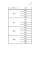
- FIG. 2 is a diagram showing an example of a bank group configuration.
- the memory 10 includes four bank groups: bank group BG0, bank group BG1, bank group BG3, and bank group BG3.
- Each bank group includes four banks, bank BA0, bank BA1, bank BA2 and bank BA3.
- the number of bank groups and the number of banks included in the memory 10 are not limited to the example shown in FIG.
- the master M issues an access request to the memory 10 and sends it to the memory control device 20.
- Examples of the master M are CPU, DMAC, Pcle, ISP and the like.
- the access request issued by the master M includes the address specification in the memory 10 in addition to the request contents such as WRITE / READ. Addresses are specified, for example, by bank group, bank, row and column. Access requests follow a given protocol. Examples of protocols are AHB (Advanced High-performance Bus), AXI (Advanced eXtensible Interface), OCP (Open Core Protocol), and the like.
- AHB Advanced High-performance Bus
- AXI Advanced eXtensible Interface
- OCP Open Core Protocol
- the memory control device 20 is provided between the master M and the memory 10.
- the memory control device 20 issues a command corresponding to the access request from the master M. Examples of commands are the READ command, the WRITE command, and the like. In addition to this, various commands such as an ACT command, a PREpb command, and a REFpb command are issued as needed.
- the memory control device 20 includes an arbiter 21, a FIFO 22 (First In First Out), a memory controller 23, and a PHY 24.
- the arbiter 21 mediates the access request from the master M.
- An example of arbitration is determining the order of accepting multiple access requests, the details of which will be described later.
- the arbiter 21 outputs the received access request to the FIFA 22 (Push).
- the FIFA 22 stores the access requests received by the arbiter 21 in order.
- the access requests stored in the FIFA 22 are fetched (POPed) by the memory controller 23 in the storage order.
- the memory controller 23 issues a command corresponding to the access request based on the arbitration result of the arbiter 21. That is, the memory controller 23 retrieves the access request from the FIFA 22 in which the access request is stored in the order of reception of the arbiter 21, and issues a command corresponding to the fetched access request. The memory controller 23 transmits the issued command to the PHY 24.
- the PHY 24 is provided between the memory controller 23 and the memory 10.
- the PHY 24 is a physical layer interface and converts a command issued by the memory controller 23 into a physical quantity.
- the PHY 24 causes an electric signal (voltage signal or the like) corresponding to a command to appear at a terminal (for example, a parallel terminal) such as an IC (not shown).
- the electrical signal is sent to the memory 10.
- the memory 10 operates according to a command issued by the memory controller 23, more specifically, an electric signal from the PHY 24. For example, an ACT command is issued and the access destination bank transitions to the Activate state (from the Idle state). A READ command is issued, and data is transferred from the memory 10 to the master M.
- the memory 10 is controlled by the memory control device 20 based on various clocks.
- the control operation clock of the memory controller 23 is referred to as a command clock.
- the operating clock for data transfer in the memory 10 is referred to as a data clock.
- the command clock frequency may be lower than the data clock frequency.
- An example of the ratio of the command clock frequency to the data clock frequency is 1: 4, for example, the command clock frequency is 800 MHz and the data clock frequency is 3200 MHz.
- the command issuance scheduling may be N parallelized (N is an integer of 2 or more), and in that case, the control of the memory controller 23 may be synchronized with a clock frequency of 1 / N of the command clock frequency.
- the operating clock of the arbiter 21 may be arbitrarily set as long as the FIFO 22 supports an asynchronous clock.
- the frequency of the operating clock of the arbiter 21 is set to, for example, the same clock frequency as the CPU system in which the latency requirement from the access request to the data is strict, or the same clock frequency as the master M having the widest data width. Unless otherwise specified, the operating clock frequency of the arbiter 21 will be described as being 1 ⁇ 2 of the command clock frequency (for example, 400 MHz).
- the arbiter 21 determines the order of accepting the access requests. If all the access destinations are in the IDLE state, the command can be issued in the shortest time regardless of which access request is received, so it is not necessary to determine the order in particular. However, if this is not the case, it is desirable to give priority to the access request that can issue the corresponding command earlier in order to improve the data transfer efficiency.
- immediate issuance of an ACT command corresponding to a further access request to a bank group (such as a row address with a different bank) that is in the ACTIVE state due to the ACT command issued immediately before may be prohibited due to restrictions or the like. be.
- the PREpb command must be issued once, and the ACT command must be issued after returning from the Prechanging state to the Idle state, which takes time. In this case, it is desirable to preferentially accept an access request to another bank group that can issue the corresponding command as soon as possible.
- the arbiter 21 accepts an access request when there is only an access request to the same bank group as the bank group that issued the command immediately before in the acceptable (selectable) access request. Withhold. In the meantime, when an access request to a different bank group is issued, the arbiter 21 accepts the access request. That is, when the arbiter 21 receives an access request to the first bank group among the plurality of bank groups, the arbiter 21 suspends the acceptance of other access requests to the first bank group. When the arbiter 21 receives an access request to a bank group other than the first bank group, the arbiter 21 releases the hold.
- the holding period may be set to be the same as the above-mentioned first period (tCCD_L).
- the arbiter 21 may count the hold period. In that case, when the arbiter 21 receives the access request to the first bank group, the arbiter 21 starts counting indicating that the first bank group is in a busy state.
- a busy state is a state that requires an ACT / PRE operation (tRAS, tRPpb, tRCD).
- the arbiter 21 releases the hold when the count value reaches a predetermined value.
- the predetermined value is set according to the holding period.
- the hold period may be set to a period until the amount of access request data stored in the FIFA 22 falls below a predetermined amount of data (threshold value). Since the access request stored in the FIFA 22 is taken out (POP) by the memory controller 23 over time, it does not wait forever and deadlock.
- POP taken out
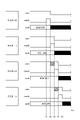
- the hold is done by masking the access request. That is, the arbiter 21 ignores the access request from the master M only during the mask period. This will be described with reference to FIGS. 3 and 4. 3 and 4 are diagrams schematically showing an example of the operation of the first method.
- FIG. 3 schematically shows an example of the timing of accepting an access request.
- the time t is indicated by the horizontal axis.
- Value indicates the issuance status of the access request, and when it is high, the access request is being issued (asserted).
- Ready indicates acceptance of the access request by the arbiter 21, and when it is high, the access request is accepted.
- Addr is an address, and the figure illustrates bank groups and banks among the elements that specify the address.
- the target of the access request from the master 0 is the access request to the bank BA0 of the bank group BG0.
- the target of the access request from the master 1 is the bank BA0 of the bank group BG1.
- the target of the access request from the master 2 is the bank BA1 of the bank group BG0.
- the target of the access request from the master 3 is the bank BA1 of the bank group BG1.
- the arbiter 21 receives an access request from the master 0 to the bank group BA0 of the bank group BG0.
- the arbiter 21 masks the access request to the bank group BG0.
- the access request from the master 2 to the bank BA1 of the bank group BG0 is masked as shown by hatching.
- the arbiter 21 does not accept the access request from the master 2 (holds the acceptance).
- the arbiter 21 receives an access request from the master 1 to the bank BA0 of the bank group BG0.
- the arbiter 21 unmasks the access request to the bank group BG0. That is, the mask of the access request from the master 2 is released. At the same time, the arbiter 21 masks the access request to the bank group BG1. In this example, the access request from the master 3 to the bank BA1 of the bank group BG1 is masked. The arbiter 21 does not accept the access request from the master 3.
- the arbiter 21 receives an access request from the master 2 to the bank BA1 of the bank group BG0.
- the arbiter 21 unmasks the access request to the bank group BG1. That is, the mask of the access request from the master 3 is released. Although not shown in the figure, if there is an access request to the bank group BG0 from another master at this time, the arbiter 21 masks the access request to the bank group BG0 again.
- the arbiter 21 receives an access request from the master 3 to the bank BA1 of the bank group BG1.
- FIG. 4 schematically shows an example of command issuance timing.
- the issued commands the ACT command and the READ command are exemplified.
- the memory controller 23 issues an ACT command to the bank group BA0 of the bank group BG0.
- This ACT command corresponds to the access request from the master 0 received at the time t1 to the time t2 in FIG.
- the memory controller 23 issues an ACT command to bank BA0 of bank group BG1.
- This ACT command corresponds to the access request from the master 1 received at the time t2 to the time t3 in FIG.
- the memory controller 23 issues a READ command to bank BA0 of bank group BG0.
- This READ command is a command following the ACT command issued at the previous time t11, and corresponds to the access request from the master 0 received at the time t1 to the time t2 in FIG.
- the memory controller 23 issues an ACT command to bank BA1 of bank group BG0.
- This ACT command corresponds to the access request from the master 2 received at the time t3 to the time t4 in FIG.
- the memory controller 23 issues a READ command to bank BA0 of bank group BG1.
- This READ command is a command following the ACT command issued at the previous time t12, and corresponds to the access request from the master 1 received at the time t2 to the time t3 in FIG.
- the memory controller 23 issues an ACT command to bank BA1 of bank group BG1.
- This ACT command corresponds to the access request from the master 3 received at the time t4 to the time t5 in FIG.
- the memory controller 23 issues a READ command to bank BA1 of bank group BG0.
- This READ command is a command following the ACT command issued at the previous time t14, and corresponds to the access request from the master 2 received at the time t3 to the time t4 in FIG.
- the memory controller 23 issues a READ command to bank BA1 of bank group BG1.
- This READ command is a command following the ACT command issued at the previous time t16, and corresponds to the access request from the master 3 received from the time t4 to the time t5 in FIG.
- the arbiter 21 masks the access request to the same bank group so as not to continuously accept the access request to the same bank group. This makes it possible to secure a command issuance interval for the same bank group.
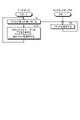
- FIG. 5 is a flowchart showing an example of the process (memory control method) executed in the first method.
- step S1 the arbiter 21 receives the access request from the master M.
- the arbiter 21 receives an access request from the master 0 to the bank group BG0.
- the received access request is stored in the FIFA 22 and taken out by the memory controller 23.
- step S2 the memory controller 23 issues a command.
- the memory controller 23 issues a command corresponding to an access request from the master 0 to the bank group BG0.
- step S3 the arbiter 21 masks the access request to the bank group and cancels the previous mask. For example, the arbiter 21 masks an access request to the bank group BG0. For example, when the access request to the bank group BG1 is received in step S1 of the previous flow and the access request to the bank group BG1 is masked in step S3, the arbiter 21 unmasks the access request to the bank group BG1.
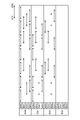
- FIG. 6 is a diagram schematically showing an example of the operation of the comparative example.
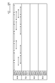
- FIG. 7 is a diagram schematically showing an example of the operation of the first method.
- FIG. 6 schematically shows an example of the timing of accepting an access request and issuing a command in the comparative example.
- Master 0, Master 1 and Master 2 are illustrated. All access requests from master 0 target bank group BG0. All access requests from the master 1 target the bank group BG1. The access request of the master 2 targets the bank group BG2.
- access requests R1 to access request R20 are referred to as access requests R1 to access request R20 and are shown in the figure.
- the access request R1, the access request R3, the access request R5, the access request R8, the access request R10, the access request R13, the access request R14, the access request R17, and the access request R18 are access requests from the master 0.
- the access request R2, access request R4, access request R6, access request R11, access request R15, and access request R19 are access requests from the master 1.
- the access request R7, access request R9, access request R12, access request R16 and access request R20 are access requests from the master 2.
- the commands issued in order corresponding to the access request R1 to the access request R20 are referred to as commands C1 to C20 and are shown in the figure.
- issuing each command requires two command clocks.
- the access request R13 and the access request R14 are continuously received, and the access request R17 and the access request R18 are also continuously received.
- the corresponding commands C13 and C14 are issued in succession, and the commands C17 and C18 are also issued in succession.
- FIG. 7 schematically shows an example of the timing of accepting an access request and issuing a command in the first method.
- the arbiter 21 After receiving the access request 13 from the master 0 to the bank group BG0, the arbiter 21 masks the access request to the bank group BG0 (illustrated by hatching). During this time, the arbiter 21 does not accept the access request from the master 0. Instead, the arbiter 21 receives an access request R14 from the master 1 to the bank group BG1. After that, the arbiter 21 sequentially receives the access request R15 from the master 2 to the bank group BG2 and the access request R16 from the master 1 to the bank group BG1.
- the arbiter 21 masks the access request to the bank group BG0, receives the access request R17 from the master 1 to the bank group BG1, and then receives the access request R18 from the master 1 to the bank group BG1 again. After that, the arbiter 21 sequentially receives the access request R19 from the master 2 to the bank group BG2 and the access request R20 from the master 0 to the bank group BG0.
- the issuance intervals of the commands C13 and C14 corresponding to the access request R13 and the access request R14, and the issuance intervals of the commands C17 and the command C18 corresponding to the access request R17 and the access request R18 are all 8 command clocks or more. , The constraint is met.
- the memory controller 23 evaluates the state of the bank that is the target of the access request fetched from the FIFA 22. The state evaluation is performed based on the command issued by the memory controller 23 immediately before.
- the memory controller 23 issues an ACT command. As a result, the bank transitions from the Idle state to the Bank Activate state. After that, the memory controller 23 further issues a WRITE command if the access request is WRITE, and issues a READ command if the access request is READ. In this way, the memory controller 23 issues one or more commands for one access request.
- the memory controller 23 includes a buffer (not shown) that holds a plurality of access requests taken out from the FIFA 22, and issues a mixture of a plurality of commands corresponding to the plurality of access requests (mixed in chronological order). For example, it is possible that the WRITE command corresponding to the access request of the first buffer and the ACT command corresponding to the access request of the second buffer can be issued at the same time.
- the issuance of a plurality of commands may conflict (collision occurs). In this case, it is necessary to decide which command issuance is prioritized.
- the memory controller 23 determines the priority of command issuance based on the statistical information of the access request.
- the statistical information is acquired when it is accepted (selected) by the arbiter 21.
- Statistical information is information that indicates the calculated value of the period during which the access request is asserted for each bank group and / or for each bank. That is, the arbiter 21 calculates the assert period from the occurrence of the access request to the acceptance of the access request for each bank group and / or for each bank.
- the memory controller 23 preferentially issues a command corresponding to one of the access requests based on the calculated value of the assert period calculated by the arbiter 21. .. For example, the memory controller 23 preferentially issues a command corresponding to the access request having the largest calculated value of the assert period among the plurality of access requests.
- the arbiter 21 obtains the calculated value of the period during which the access request is asserted for each bank group.
- the calculated value may be an additive value during the period during which the access request is asserted. If the access request follows AXI (an example of a protocol), the arbiter 21 adds the period during which the AWVALUE, ARVALUE signals are asserted (eg, high). The arbiter 21 subtracts or resets (clears 0) the calculated value of the bank group for which there is no access request from any master M.
- the arbiter 21 When the calculated value exceeds the threshold value, the arbiter 21 notifies the memory controller 23 of the bank group.
- the notification may be performed by adding information to the access request via the FIFA 22, or may be performed on a channel different from the FIFA 22.
- the memory controller 23 always gives priority to issuing commands to the bank group notified by the arbiter 21. If there are restrictions on the command issuance timing due to standards, etc., the command may be issued in the shortest time within the range that does not violate it.
- the arbiter 21 obtains a calculated value for the period during which the access request is asserted for each bank.
- the arbiter 21 notifies the memory controller 23 of the bank.
- the memory controller 23 always gives priority to issuing a command to the bank notified by the arbiter 21.
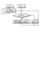
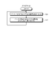
- FIG. 8 is a flowchart showing an example of the process (memory control method) executed in the second method.
- step S11 the arbiter 21 calculates the calculated value of the assert period. For example, the arbiter 21 calculates the calculated value of the assert period of the access request for each of the bank group BG0 to the bank group BG3. The calculated value is sent to the memory controller 23. For example, a bank group whose calculated value exceeds the threshold value is notified to the memory controller 23. The arbiter 21 may calculate the calculated value of the assert period of the access request for each of banks BA1 to BA3. In that case, the memory controller 23 is notified of the bank whose calculated value exceeds the threshold value.
- step S12 the memory controller 23 determines whether or not the command issuance conflicts. If the command issuance conflicts (Yes in step S12), the process proceeds to step S13. If not (No in step S12), the process proceeds to step S14.
- step S13 the memory controller 23 gives priority to issuing one of the commands based on the calculated value. For example, when the bank group BG0 is notified from the arbiter 21, the memory controller 23 preferentially issues a command corresponding to an access request to the bank group BG0. When the bank BA1 is notified from the arbiter 21, the memory controller 23 preferentially issues a command corresponding to the access request to the bank BA1.
- step S14 the memory controller 23 issues a command. That is, in this case, since there is no conflict in issuing commands, the memory controller 23 issues commands in order as usual.
- FIG. 9 schematically shows an example of the frequency of access requests for each bank group.
- the arrows indicate that the bank is in a busy state requiring an ACT / PRE operation (tRAS, tRPpb, tRCD).
- ACT ACT / PRE operation
- tRPpb ACT / PRE operation
- tRCD ACT / PRE operation
- the frequency of access requests to the bank BA0 of the bank group BG0 is the highest. Therefore, the command issuance (ACT, WRITE, READ, PREpb) to the bank BA0 of the bank group BG0 is prioritized.
- FIG. 10 schematically shows an example of the frequency of access requests for each bank.
- the frequency of access requests to the bank group BG0 is the highest. Therefore, the command issuance to the bank group BG0 has priority.
- the issuance frequency of the access request having the burst length 32 is 50% for the bank group BG0 and 25% for each of the bank group BG1 and the bank group BG2.
- the data transfer efficiency of the surplus bank group BG0 becomes 50%, and the overall efficiency becomes 80. %Become.
- the access request to the bank group BG0 is always prioritized, and the commands are issued in the order of bank group BG0, bank group BG1, bank group BG0, bank group BG2, bank group BG0, and so on. publish.
- bank group BG0 and bank group BG2 as the third command issuance option, but the command issuance to the bank group BG0 is prioritized.
- bank group BG0 and bank group BG1 as the fifth command issuance option, but the command issuance to the bank group BG0 is prioritized. After that, the data transfer efficiency becomes 100% by repeating the process.
- the arbiter 21 may accept a plurality of access requests in an order according to the burst length of each access request. Examples of burst lengths are burst length 16 and burst length 32. The command required to issue the command corresponding to the access request of any burst length has the same period (number of command clocks).
- Addresses such as AXI and AHB are generally byte addresses, and if the data width is 64 bits, the address is a multiple of 8, and if the data width is 128 bits, the address is a multiple of 16.
- the data width ⁇ length Since data is continuously handled by the data width ⁇ length, if the data width is 128 bits and the length is 16, 2048 bits of data can be transferred with one access request. For example, when the number of data pins per channel is 16, 256 bits of data are transferred by the WRITE command having a burst length of 16. In the WRITE command with a burst length of 32, 512 bits of data are transferred. The same applies to the READ command.
- the data width is 128 bits and the length is 16, 2048 bits of data can be transferred with one access request, but whether it can be divided into burst lengths depends on the start address.
- the address is 512 bit aligned, that is, a byte address that is a multiple of 64
- 2048 bit can be transferred with four commands with a burst length of 32, such as 512 + 512 + 512 + 512.
- the address is not 512-bit aligned, but the byte address is a multiple of 32, 2048-bit can be transferred with five commands with a burst length of 16 and a burst length of 32, such as 256 + 512 + 512 + 512 + 256.
- the arbiter 21 or the memory controller 23 determines whether the burst length is the burst length 16 or the burst length 32 from the address, data width and length indicated in the access request (AXI, AHB, etc.). Can be uniquely determined. Therefore, the division may be performed by any of the front stage of the arbiter 21, the arbiter 21, the front stage of the memory controller 23, and the memory controller 23. What is important is that the arbiter 21 can grasp whether the access request that is about to be selected (acceptable) is an access request having a burst length of 16 or an access request having a burst length of 32.
- the arbiter 21 sets the burst length as the next access request to be selected. Priority is given to the access request that becomes 32. That is, the arbiter 21 performs burst transfer at the time of writing data to the memory 10 (WRITE) and reading data from the memory 10 (READ) based on the address, data width, and length indicated in the access request. An access request whose burst length is the first burst length (for example, burst length 16) and an access request whose burst length is longer than the first burst length (for example, burst length 32). Accept in order.
- This third method can also be implemented independently of the above-mentioned first method, and by using it in combination with the first method (implemented in parallel), the data transfer efficiency can be further improved.
- FIG. 11 is a flowchart showing an example of the process (memory control method) executed in the third method.
- the arbiter 21 receives an access request having a burst length of 16.
- the arbiter 21 receives at least one access request having a burst length of 32. Even if the processes of steps S21 and S22 are repeatedly executed, the data transfer efficiency can be further improved.
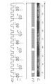
- 12 and 13 are diagrams schematically showing the operation of the comparative example. Only the command corresponding to the access request having a burst length of 16 is issued. From the viewpoint of facilitating understanding and the like, the read latency (RL) is described as 0 so that the free space for commands and data transfer is shown side by side.
- RL read latency
- command C31, command C33, command C35, command C37 and command C39 for bank group BG0 and command C32, command C34, command C36 and command C38 for bank group BG1 issue commands. It is issued alternately at intervals (for example, tCCD_S). The entire data transfer bandwidth (ie, 100%) is occupied by data D31 to data D9 transferred in response to the command.
- the band for issuing commands is also filled, and other commands (for example, ACT commands) cannot be issued.
- two ACT commands (ACT1 and ACT2) for the bank group BG2 are sequentially issued between the issuance of the command C34 and the issuance of the command C35.
- ACT1 and ACT2 are sequentially issued between the issuance of the command C34 and the issuance of the command C35.
- command C41, command C43, command C44 and command C47 are issued to the bank group BG0.
- Command C41, command C43, and command C47 are issued in response to an access request having a burst length of 16.
- the command C44 is issued in response to an access request having a burst length of 32.
- Data D41, data D43, data D44 and data D47 are transferred in response to these commands.
- the data D44 is separately transferred to the data D44-1 and the data D44-2.
- Command C42, command C45 and command C46 are issued to the bank group BG1.
- the command C45 is issued in response to an access request having a burst length of 16.
- the command C42 is issued in response to an access request having a burst length of 32.
- the command C46 may be issued in response to any access request having a burst length, and in this example, the command C46 is shown to correspond to an access request having a burst length of 32.
- Data D42, data D45 and data D46 are transferred in response to these commands.
- the data D42 is transferred separately to the data D42-1 and the data D42-2. The same applies to the data D46.
- the ACT command for the bank group BG2 is issued between the issuance of the command C43 and the issuance of the command C44. Even in this case, there is no band in which data is not transferred. Further, an ACT command for the bank group BG3 is issued between the issuance of the command C45 and the issuance of the command C46. Even in this case, there is no band in which data is not transferred. As a result, the data transfer band can be set to 100%.
- the ACT command can be issued by issuing a command corresponding to the access request having a burst length of 32 without crowding the access requests having a burst length of 16.
- the access request column (request example) may be held in the buffer in the previous stage of the arbiter 21 and the access requests may be rearranged. For example, if there are two or more bank groups, banks, and rows among the addresses (bank groups, banks, rows, columns), they may be sorted so that they are issued consecutively. As a result, the number of times the PREpb and ACT commands are issued can be reduced, and the data transfer command can be issued faster.
- the arbiter 21 may be divided into a plurality of layers (for example, a tournament) until the order is determined. For example, access requests from all masters M are classified by bank in the first layer, and access requests are selected. If the number of banks is 16, a maximum of 16 access requests are selected. Next, the access request selected in the first layer is classified by bank group in the second layer, and the access request is selected. When the number of bank groups is 4, a maximum of 4 access requests are selected. Finally, the order is determined between the access requests selected in the second hierarchy.
- a tournament for example, access requests from all masters M are classified by bank in the first layer, and access requests are selected. If the number of banks is 16, a maximum of 16 access requests are selected. Next, the access request selected in the first layer is classified by bank group in the second layer, and the access request is selected. When the number of bank groups is 4, a maximum of 4 access requests are selected. Finally, the order is determined between the access requests selected in the second hierarchy.
- statistical information may be notified from the master M to the arbiter 21.
- the arbiter 21 may add up the information notified from the master M (incorporate it into the calculation) to obtain the entire statistical information.
- the statistical information may be notified (returned) from the CPU to the arbiter 21 according to the application.
- the arbiter 21 may obtain the entire statistical information by adding up the information notified by the CPU and the statistical information that the CPU itself accesses the arbiter 21 (for example, when the program area is in the memory 10).
- the aligned access requests may be rearranged by the memory controller 23.
- the memory controller 20 has an arbiter 21 and an arbiter 21 for receiving an access request to the memory 10 including a plurality of bank groups each having a plurality of banks. It includes a memory controller 23 that issues a command corresponding to the access request received by the 21.
- the arbiter 21 receives an access request to the first bank group among the plurality of bank groups, the arbiter 21 suspends the acceptance of other access requests to the first bank group (for example, masks the access request).
- access requests to the same bank group are not continuously accepted. For example, by accepting access requests to other bank groups in the meantime, it is possible to suppress a decrease in data transfer efficiency while ensuring a command issuance interval for the same bank group.
- the arbiter 21 may release the hold (for example, remove the mask) when it receives an access request to a bank group other than the first bank group.
- the command issuance interval for the same bank group can be set.
- the arbiter 21 may start counting indicating that the first tapirus group is busy, and may release the hold when the count value reaches a predetermined value. .. For example, in this way, the command issuance interval for the same bank group can be secured.
- the memory control device 20 includes a FIFA 22 that stores access requests received by the arbiter 21, and the memory controller 23 takes out and takes out the access requests stored in the FIFA 22.
- the arbiter 21 may issue a command corresponding to the access request and release the hold when the amount of data of the access request stored in the FIFA 22 is less than the predetermined amount of data. As a result, it is possible to secure a command issuance interval for the same bank group while preventing the hold from being deadlocked.
- the arbiter 21 calculates the assert period from the occurrence of the access request to the acceptance of the access request at least for each bank group, and the memory controller 23 corresponds to a plurality of access requests.
- the command corresponding to any access request may be preferentially issued based on the calculated value of the assert period calculated by the arbiter 21.
- the memory controller 23 may issue the command corresponding to the access request having the largest calculated value of the assert period among the plurality of access requests with priority.
- the arbiter 21 may calculate the assert period for each bank. As a result, priority is given to issuing commands to bank groups and / or banks with a large statistical bias, and it is possible to suppress a decrease in data transfer efficiency by that amount.
- the arbiter 21 writes data to and from memory 10 based on, for example, the address, data width and length indicated in the access request.
- the access request that becomes 32) may be accepted in this order. This makes it possible to issue commands such as ACT commands and suppress a decrease in data transfer efficiency, as compared with the case where access requests having a first burst length are concentrated.
- the arbiter 21 accepts an access request to the memory 10 including a plurality of bank groups each having a plurality of banks (step S1), and the memory controller 23 receives an access received by the arbiter 21.
- the arbiter 21 receives the access request to the first bank group among the plurality of bank groups, the arbiter 21 includes issuing a command corresponding to the request (step S2), and the other to the first bank group. (For example, masking the access request) (step S3).
- a memory control method can also suppress a decrease in data transfer efficiency.
- the present technology can also take the following configurations.
- An arbiter that accepts access requests to memory containing multiple bank groups, each with multiple banks, A memory controller that issues a command corresponding to the access request received by the arbiter, and Equipped with When the arbiter receives an access request to the first bank group among the plurality of bank groups, the arbiter suspends acceptance of other access requests to the first bank group. Memory control device.
- (3) The arbiter When the access request to the first bank group is received, the count indicating that the first bank group is in a busy state is started, and the count is started.
- the memory control device When the value of the count reaches a predetermined value, the hold is released.
- the memory control device according to (1) or (2).
- a FIFO that stores the access requests received by the arbiter is provided.
- the memory controller retrieves the access request stored in the FIFO, issues a command corresponding to the fetched access request, and issues a command.
- the arbiter releases the hold when the amount of access request data stored in the FIFO falls below a predetermined amount of data.
- the memory control device according to any one of (1) to (3).
- the arbiter calculates the assert period from the occurrence of the access request to the acceptance of the access request at least for each bank group.
- the memory controller issues the command corresponding to one of the access requests with priority based on the calculated value of the assert period calculated by the arbiter.
- the memory control device according to any one of (1) to (4). (6)
- the memory controller preferentially issues a command corresponding to the access request having the largest calculated value of the assert period among the plurality of access requests.
- the memory control device according to (5).
- the arbiter calculates the assert period for each bank.
- the arbiter is an access request in which the burst length of the burst transfer performed when writing data to the memory and reading data from the memory is the first burst length, and the burst length is the first burst. Accepts access requests that have a second burst length that is longer than the length, in that order.
- the memory control device according to any one of (1) to (7).
- the arbiter is an access request in which the burst length is the first burst length and an access in which the burst length is the second burst length, based on the address, data width and length indicated in the access request. Accept requests in this order, The memory control device according to (8).
- the arbiter accepts a request to access memory containing multiple bank groups, each with multiple banks.
- It is a memory control method including When the arbiter receives an access request to the first bank group among the plurality of bank groups, the arbiter suspends acceptance of other access requests to the first bank group. Memory control method.
- Memory 20 Memory Controller 21 Arbiter 22 FIFO 23 Memory controller 100 Memory control system M master
Landscapes
- Engineering & Computer Science (AREA)
- Theoretical Computer Science (AREA)
- Physics & Mathematics (AREA)
- General Engineering & Computer Science (AREA)
- General Physics & Mathematics (AREA)
- Human Computer Interaction (AREA)
- Memory System (AREA)
- Multi Processors (AREA)
- Dram (AREA)
Abstract
Description
1.序
2.実施形態
2.1 第1の手法の例
2.2 第2の手法の例
2.3 第3の手法の例
3.変形例
4.効果
DRAM(Dynamic Random Access Memory)の高速化に伴い、バンク数を増やし、DRAMメモリセルの欠点であるページオープン・クローズのオーバーヘッドを隠蔽してWRITE/READを連続して行うことができるようになった。この手法は、バンクインターリーブ等とも称される。
図1は、実施形態に係るメモリ制御装置が用いられるメモリシステムの概略構成の例を示す図である。メモリシステム100は、メモリ10と、マスターMと、メモリ制御装置20とを含む。この例では、複数のマスターMが存在し、各マスターMを区別できるように、マスター0、マスター1、マスターM及びマスター3と称し図示する。なお、マスターMの数は、図1に示される例に限定されない。
先にも述べたが、複数のマスターMからの複数のアクセス要求が存在する場合、アービター21は、アクセス要求の受け付け順序を決定する。アクセス先がいずれもIDLE状態であれば、いずれのアクセス要求を受け付けても最短でコマンド発行が可能であるのでとくに順序決定しなくてよい。ただし、そうでない場合には、対応するコマンド発行が早く行えるアクセス要求を優先して受け付けることが、データ転送効率を高める意味で望ましい。
図1に戻り、メモリコントローラ23についてさらに説明する。メモリコントローラ23の動作は周知であるが、理解を容易にするために、いくつかの動作の例を説明する。メモリコントローラ23は、FIFO22から取り出したアクセス要求の対象となるバンクの状態(ステート)を評価する。状態評価は、メモリコントローラ23が直前までに発行したコマンドに基づいて行われる。
図1に戻り、アービター21は、複数のアクセス要求を、それぞれのアクセス要求のバースト長に応じた順で受け付けてよい。バースト長の例は、バースト長16及びバースト長32である。いずれのバースト長のアクセス要求に対応するコマンドも、発行に要する期間(コマンドクロック数)は同じである。
本開示は、上記の実施形態に限定されない。いくつかの変形例について述べる。
以上説明したメモリ制御装置20は、例えば次のように特定される。図1~図5及び図7等を参照して説明したように、メモリ制御装置20は、各々が複数のバンクを有する複数のバンクグループを含むメモリ10へのアクセス要求を受け付けるアービター21と、アービター21が受け付けたアクセス要求に対応するコマンドを発行するメモリコントローラ23と、を備える。アービター21は、複数のバンクグループのうちの第1のバンクグループへのアクセス要求を受け付けると、第1のバンクグループへの他のアクセス要求の受け付けを保留する(例えばアクセス要求をマスクする)。
(1)
各々が複数のバンクを有する複数のバンクグループを含むメモリへのアクセス要求を受け付けるアービターと、
前記アービターが受け付けたアクセス要求に対応するコマンドを発行するメモリコントローラと、
を備え、
前記アービターは、前記複数のバンクグループのうちの第1のバンクグループへのアクセス要求を受け付けると、前記第1のバンクグループへの他のアクセス要求の受け付けを保留する、
メモリ制御装置。
(2)
前記アービターは、前記第1のバンクグループ以外のバンクグループへのアクセス要求を受け付けると、前記保留を解除する、
(1)に記載のメモリ制御装置。
(3)
前記アービターは、
前記第1のバンクグループへのアクセス要求を受け付けると、前記第1のバンクグループがビジー状態であることを示すカウントを開始し、
前記カウントの値が所定値になると、前記保留を解除する、
(1)又は(2)に記載のメモリ制御装置。
(4)
前記アービターによって受け付けられたアクセス要求を蓄積するFIFOを備え、
前記メモリコントローラは、前記FIFOに蓄積されたアクセス要求を取り出し、取り出したアクセス要求に対応するコマンドを発行し、
前記アービターは、前記FIFOに蓄積されているアクセス要求のデータ量が所定のデータ量を下回ると、前記保留を解除する、
(1)~(3)のいずれかに記載のメモリ制御装置。
(5)
前記アービターは、アクセス要求が発生してから受け付けるまでのアサート期間を、少なくともバンクグループごとに算出し、
前記メモリコントローラは、複数のアクセス要求に対応するコマンドの発行が衝突する場合、前記アービターによって算出された前記アサート期間の算出値に基づいて、いずれかのアクセス要求に対応するコマンドを優先して発行する、
(1)~(4)のいずれかに記載のメモリ制御装置。
(6)
前記メモリコントローラは、前記複数のアクセス要求のうち、前記アサート期間の算出値が最も大きいアクセス要求に対応するコマンドを優先して発行する、
(5)に記載のメモリ制御装置。
(7)
前記アービターは、前記アサート期間をバンクごとに算出する、
(5)又は(6)に記載のメモリ制御装置。
(8)
前記アービターは、前記メモリへのデータの書き込み及びメモリからのデータの読み出しの際に行われるバースト転送のバースト長が第1のバースト長になるアクセス要求、及び、前記バースト長が前記第1のバースト長よりも長い第2のバースト長になるアクセス要求をこの順に受け付ける、
(1)~(7)のいずれかに記載のメモリ制御装置。
(9)
前記アービターは、アクセス要求に示されるアドレス、データ幅及び長さに基づいて、前記バースト長が前記第1のバースト長になるアクセス要求、及び、前記バースト長が前記第2のバースト長になるアクセス要求をこの順に受け付ける、
(8)に記載のメモリ制御装置。
(10)
アービターが、各々が複数のバンクを有する複数のバンクグループを含むメモリへのアクセス要求を受け付けることと、
メモリコントローラが、前記アービターが受け付けたアクセス要求に対応するコマンドを発行することと、
を含むメモリ制御方法であって、
前記アービターは、前記複数のバンクグループのうちの第1のバンクグループへのアクセス要求を受け付けると、前記第1のバンクグループへの他のアクセス要求の受け付けを保留する、
メモリ制御方法。
20 メモリ制御装置
21 アービター
22 FIFO
23 メモリコントローラ
100 メモリ制御システム
M マスター
Claims (10)
- 各々が複数のバンクを有する複数のバンクグループを含むメモリへのアクセス要求を受け付けるアービターと、
前記アービターが受け付けたアクセス要求に対応するコマンドを発行するメモリコントローラと、
を備え、
前記アービターは、前記複数のバンクグループのうちの第1のバンクグループへのアクセス要求を受け付けると、前記第1のバンクグループへの他のアクセス要求の受け付けを保留する、
メモリ制御装置。 - 前記アービターは、前記第1のバンクグループ以外のバンクグループへのアクセス要求を受け付けると、前記保留を解除する、
請求項1に記載のメモリ制御装置。 - 前記アービターは、
前記第1のバンクグループへのアクセス要求を受け付けると、前記第1のバンクグループがビジー状態であることを示すカウントを開始し、
前記カウントの値が所定値になると、前記保留を解除する、
請求項1に記載のメモリ制御装置。 - 前記アービターによって受け付けられたアクセス要求を蓄積するFIFOを備え、
前記メモリコントローラは、前記FIFOに蓄積されたアクセス要求を取り出し、取り出したアクセス要求に対応するコマンドを発行し、
前記アービターは、前記FIFOに蓄積されているアクセス要求のデータ量が所定のデータ量を下回ると、前記保留を解除する、
請求項1に記載のメモリ制御装置。 - 前記アービターは、アクセス要求が発生してから受け付けるまでのアサート期間を、少なくともバンクグループごとに算出し、
前記メモリコントローラは、複数のアクセス要求に対応するコマンドの発行が衝突する場合、前記アービターによって算出された前記アサート期間の算出値に基づいて、いずれかのアクセス要求に対応するコマンドを優先して発行する、
請求項1に記載のメモリ制御装置。 - 前記メモリコントローラは、前記複数のアクセス要求のうち、前記アサート期間の算出値が最も大きいアクセス要求に対応するコマンドを優先して発行する、
請求項5に記載のメモリ制御装置。 - 前記アービターは、前記アサート期間をバンクごとに算出する、
請求項5に記載のメモリ制御装置。 - 前記アービターは、前記メモリへのデータの書き込み及びメモリからのデータの読み出しの際に行われるバースト転送のバースト長が第1のバースト長になるアクセス要求、及び、前記バースト長が前記第1のバースト長よりも長い第2のバースト長になるアクセス要求をこの順に受け付ける、
請求項1に記載のメモリ制御装置。 - 前記アービターは、アクセス要求に示されるアドレス、データ幅及び長さに基づいて、前記バースト長が前記第1のバースト長になるアクセス要求、及び、前記バースト長が前記第2のバースト長になるアクセス要求をこの順に受け付ける、
請求項8に記載のメモリ制御装置。 - アービターが、各々が複数のバンクを有する複数のバンクグループを含むメモリへのアクセス要求を受け付けることと、
メモリコントローラが、前記アービターが受け付けたアクセス要求に対応するコマンドを発行することと、
を含むメモリ制御方法であって、
前記アービターは、前記複数のバンクグループのうちの第1のバンクグループへのアクセス要求を受け付けると、前記第1のバンクグループへの他のアクセス要求の受け付けを保留する、
メモリ制御方法。
Priority Applications (2)
| Application Number | Priority Date | Filing Date | Title |
|---|---|---|---|
| US18/258,349 US20240302969A1 (en) | 2020-12-28 | 2021-12-13 | Memory control device and memory control method |
| CN202180087192.2A CN116670657A (zh) | 2020-12-28 | 2021-12-13 | 存储器控制装置及存储器控制方法 |
Applications Claiming Priority (2)
| Application Number | Priority Date | Filing Date | Title |
|---|---|---|---|
| JP2020218395A JP2022103643A (ja) | 2020-12-28 | 2020-12-28 | メモリ制御装置及びメモリ制御方法 |
| JP2020-218395 | 2020-12-28 |
Publications (1)
| Publication Number | Publication Date |
|---|---|
| WO2022145209A1 true WO2022145209A1 (ja) | 2022-07-07 |
Family
ID=82260455
Family Applications (1)
| Application Number | Title | Priority Date | Filing Date |
|---|---|---|---|
| PCT/JP2021/045827 Ceased WO2022145209A1 (ja) | 2020-12-28 | 2021-12-13 | メモリ制御装置及びメモリ制御方法 |
Country Status (4)
| Country | Link |
|---|---|
| US (1) | US20240302969A1 (ja) |
| JP (1) | JP2022103643A (ja) |
| CN (1) | CN116670657A (ja) |
| WO (1) | WO2022145209A1 (ja) |
Citations (1)
| Publication number | Priority date | Publication date | Assignee | Title |
|---|---|---|---|---|
| JP2018136592A (ja) * | 2017-02-20 | 2018-08-30 | 日本電気株式会社 | メモリ制御装置 |
Family Cites Families (6)
| Publication number | Priority date | Publication date | Assignee | Title |
|---|---|---|---|---|
| US6119207A (en) * | 1998-08-20 | 2000-09-12 | Seiko Epson Corporation | Low priority FIFO request assignment for DRAM access |
| US6393534B1 (en) * | 1999-09-27 | 2002-05-21 | Ati International Srl | Scheduler for avoiding bank conflicts in issuing concurrent requests to main memory |
| US7111143B2 (en) * | 2003-12-30 | 2006-09-19 | Infineon Technologies Ag | Burst mode implementation in a memory device |
| US7328315B2 (en) * | 2005-02-03 | 2008-02-05 | International Business Machines Corporation | System and method for managing mirrored memory transactions and error recovery |
| US9690482B2 (en) * | 2014-11-03 | 2017-06-27 | Arm Limited | Data storage organisation technique |
| US9639280B2 (en) * | 2015-06-18 | 2017-05-02 | Advanced Micro Devices, Inc. | Ordering memory commands in a computer system |
-
2020
- 2020-12-28 JP JP2020218395A patent/JP2022103643A/ja active Pending
-
2021
- 2021-12-13 US US18/258,349 patent/US20240302969A1/en not_active Abandoned
- 2021-12-13 CN CN202180087192.2A patent/CN116670657A/zh active Pending
- 2021-12-13 WO PCT/JP2021/045827 patent/WO2022145209A1/ja not_active Ceased
Patent Citations (1)
| Publication number | Priority date | Publication date | Assignee | Title |
|---|---|---|---|---|
| JP2018136592A (ja) * | 2017-02-20 | 2018-08-30 | 日本電気株式会社 | メモリ制御装置 |
Also Published As
| Publication number | Publication date |
|---|---|
| JP2022103643A (ja) | 2022-07-08 |
| CN116670657A (zh) | 2023-08-29 |
| US20240302969A1 (en) | 2024-09-12 |
Similar Documents
| Publication | Publication Date | Title |
|---|---|---|
| JP4369660B2 (ja) | バンク衝突回避機能を備える動的ランダムアクセスメモリシステム | |
| US10684969B2 (en) | Command arbitration for high speed memory interfaces | |
| JP4742116B2 (ja) | アウトオブオーダdramシーケンサ | |
| KR20210021302A (ko) | 메모리 제어기에서의 리프레시 방식 | |
| JP4737438B2 (ja) | 複数の処理ユニットでリソースを共有する情報処理装置 | |
| US20160062930A1 (en) | Bus master, bus system, and bus control method | |
| KR20030053454A (ko) | Dram 기반의 랜덤 액세스 메모리 서브시스템에서 트리메모리 액세스에 대한 퍼포먼스를 향상시키기 위한다중-뱅크 스케쥴링 | |
| US12073114B2 (en) | Stacked command queue | |
| TW201828037A (zh) | 用於使資料元件列表能夠有高讀取率之系統及方法 | |
| US11652761B2 (en) | Switch for transmitting packet, network on chip having the same, and operating method thereof | |
| JP2014035628A (ja) | 情報処理装置、メモリ制御装置およびその制御方法 | |
| CN103150216A (zh) | 一种SoC集成的多端口DDR2/3调度器及调度方法 | |
| US7913013B2 (en) | Semiconductor integrated circuit | |
| WO2022145209A1 (ja) | メモリ制御装置及びメモリ制御方法 | |
| EP3270294B1 (en) | Command arbitration for high-speed memory interfaces | |
| JP3384770B2 (ja) | コマンド・スタッキングを有する高帯域幅で狭い入出力のメモリ装置 | |
| CN102405466B (zh) | 存储控制装置及其控制方法 | |
| Jang et al. | Application-aware NoC design for efficient SDRAM access | |
| JP7802968B2 (ja) | 擬似チャネルサポートを備えたメモリコントローラ | |
| CN113495858B (zh) | 一种同步总线访存的仲裁系统及仲裁方法 | |
| JP2004310394A (ja) | Sdramアクセス制御装置 | |
| CN112988654A (zh) | 适用于哈希算法的电路系统 | |
| CN119807098B (zh) | 一种多通道闪存阵列控制器硬件系统及其实现方法 | |
| US20250232801A1 (en) | Memory control device | |
| CN120104528B (zh) | 近存计算架构中主控与近存加速器异构执行方法及系统 |
Legal Events
| Date | Code | Title | Description |
|---|---|---|---|
| 121 | Ep: the epo has been informed by wipo that ep was designated in this application |
Ref document number: 21915070 Country of ref document: EP Kind code of ref document: A1 |
|
| WWE | Wipo information: entry into national phase |
Ref document number: 18258349 Country of ref document: US |
|
| WWE | Wipo information: entry into national phase |
Ref document number: 202180087192.2 Country of ref document: CN |
|
| NENP | Non-entry into the national phase |
Ref country code: DE |
|
| 122 | Ep: pct application non-entry in european phase |
Ref document number: 21915070 Country of ref document: EP Kind code of ref document: A1 |