WO2022130696A1 - シリコンウェーハの研磨方法及びシリコンウェーハの製造方法 - Google Patents
シリコンウェーハの研磨方法及びシリコンウェーハの製造方法 Download PDFInfo
- Publication number
- WO2022130696A1 WO2022130696A1 PCT/JP2021/031247 JP2021031247W WO2022130696A1 WO 2022130696 A1 WO2022130696 A1 WO 2022130696A1 JP 2021031247 W JP2021031247 W JP 2021031247W WO 2022130696 A1 WO2022130696 A1 WO 2022130696A1
- Authority
- WO
- WIPO (PCT)
- Prior art keywords
- polishing
- silicon wafer
- liquid
- polishing step
- head
- Prior art date
- Legal status (The legal status is an assumption and is not a legal conclusion. Google has not performed a legal analysis and makes no representation as to the accuracy of the status listed.)
- Ceased
Links
Images


Classifications
-
- B—PERFORMING OPERATIONS; TRANSPORTING
- B24—GRINDING; POLISHING
- B24B—MACHINES, DEVICES, OR PROCESSES FOR GRINDING OR POLISHING; DRESSING OR CONDITIONING OF ABRADING SURFACES; FEEDING OF GRINDING, POLISHING, OR LAPPING AGENTS
- B24B37/00—Lapping machines or devices; Accessories
- B24B37/04—Lapping machines or devices; Accessories designed for working plane surfaces
- B24B37/042—Lapping machines or devices; Accessories designed for working plane surfaces operating processes therefor
-
- B—PERFORMING OPERATIONS; TRANSPORTING
- B24—GRINDING; POLISHING
- B24B—MACHINES, DEVICES, OR PROCESSES FOR GRINDING OR POLISHING; DRESSING OR CONDITIONING OF ABRADING SURFACES; FEEDING OF GRINDING, POLISHING, OR LAPPING AGENTS
- B24B37/00—Lapping machines or devices; Accessories
- B24B37/04—Lapping machines or devices; Accessories designed for working plane surfaces
- B24B37/042—Lapping machines or devices; Accessories designed for working plane surfaces operating processes therefor
- B24B37/044—Lapping machines or devices; Accessories designed for working plane surfaces operating processes therefor characterised by the composition of the lapping agent
-
- B—PERFORMING OPERATIONS; TRANSPORTING
- B24—GRINDING; POLISHING
- B24B—MACHINES, DEVICES, OR PROCESSES FOR GRINDING OR POLISHING; DRESSING OR CONDITIONING OF ABRADING SURFACES; FEEDING OF GRINDING, POLISHING, OR LAPPING AGENTS
- B24B37/00—Lapping machines or devices; Accessories
- B24B37/11—Lapping tools
- B24B37/12—Lapping plates for working plane surfaces
-
- B—PERFORMING OPERATIONS; TRANSPORTING
- B24—GRINDING; POLISHING
- B24B—MACHINES, DEVICES, OR PROCESSES FOR GRINDING OR POLISHING; DRESSING OR CONDITIONING OF ABRADING SURFACES; FEEDING OF GRINDING, POLISHING, OR LAPPING AGENTS
- B24B53/00—Devices or means for dressing or conditioning abrasive surfaces
- B24B53/017—Devices or means for dressing, cleaning or otherwise conditioning lapping tools
-
- B—PERFORMING OPERATIONS; TRANSPORTING
- B24—GRINDING; POLISHING
- B24B—MACHINES, DEVICES, OR PROCESSES FOR GRINDING OR POLISHING; DRESSING OR CONDITIONING OF ABRADING SURFACES; FEEDING OF GRINDING, POLISHING, OR LAPPING AGENTS
- B24B57/00—Devices for feeding, applying, grading or recovering grinding, polishing or lapping agents
- B24B57/02—Devices for feeding, applying, grading or recovering grinding, polishing or lapping agents for feeding of fluid, sprayed, pulverised, or liquefied grinding, polishing or lapping agents
-
- H—ELECTRICITY
- H10—SEMICONDUCTOR DEVICES; ELECTRIC SOLID-STATE DEVICES NOT OTHERWISE PROVIDED FOR
- H10P—GENERIC PROCESSES OR APPARATUS FOR THE MANUFACTURE OR TREATMENT OF DEVICES COVERED BY CLASS H10
- H10P72/00—Handling or holding of wafers, substrates or devices during manufacture or treatment thereof
- H10P72/04—Apparatus for manufacture or treatment
- H10P72/0402—Apparatus for fluid treatment
- H10P72/0404—Apparatus for fluid treatment for general liquid treatment, e.g. etching followed by cleaning
-
- H—ELECTRICITY
- H10—SEMICONDUCTOR DEVICES; ELECTRIC SOLID-STATE DEVICES NOT OTHERWISE PROVIDED FOR
- H10P—GENERIC PROCESSES OR APPARATUS FOR THE MANUFACTURE OR TREATMENT OF DEVICES COVERED BY CLASS H10
- H10P72/00—Handling or holding of wafers, substrates or devices during manufacture or treatment thereof
- H10P72/04—Apparatus for manufacture or treatment
- H10P72/0402—Apparatus for fluid treatment
- H10P72/0406—Apparatus for fluid treatment for cleaning followed by drying, rinsing, stripping, blasting or the like
- H10P72/0411—Apparatus for fluid treatment for cleaning followed by drying, rinsing, stripping, blasting or the like for wet cleaning or washing
-
- H—ELECTRICITY
- H10—SEMICONDUCTOR DEVICES; ELECTRIC SOLID-STATE DEVICES NOT OTHERWISE PROVIDED FOR
- H10P—GENERIC PROCESSES OR APPARATUS FOR THE MANUFACTURE OR TREATMENT OF DEVICES COVERED BY CLASS H10
- H10P72/00—Handling or holding of wafers, substrates or devices during manufacture or treatment thereof
- H10P72/04—Apparatus for manufacture or treatment
- H10P72/0402—Apparatus for fluid treatment
- H10P72/0418—Apparatus for fluid treatment for etching
- H10P72/0422—Apparatus for fluid treatment for etching for wet etching
- H10P72/0424—Apparatus for fluid treatment for etching for wet etching using mainly spraying means, e.g. nozzles
-
- H—ELECTRICITY
- H10—SEMICONDUCTOR DEVICES; ELECTRIC SOLID-STATE DEVICES NOT OTHERWISE PROVIDED FOR
- H10P—GENERIC PROCESSES OR APPARATUS FOR THE MANUFACTURE OR TREATMENT OF DEVICES COVERED BY CLASS H10
- H10P72/00—Handling or holding of wafers, substrates or devices during manufacture or treatment thereof
- H10P72/04—Apparatus for manufacture or treatment
- H10P72/0428—Apparatus for mechanical treatment or grinding or cutting
-
- H—ELECTRICITY
- H10—SEMICONDUCTOR DEVICES; ELECTRIC SOLID-STATE DEVICES NOT OTHERWISE PROVIDED FOR
- H10P—GENERIC PROCESSES OR APPARATUS FOR THE MANUFACTURE OR TREATMENT OF DEVICES COVERED BY CLASS H10
- H10P72/00—Handling or holding of wafers, substrates or devices during manufacture or treatment thereof
- H10P72/04—Apparatus for manufacture or treatment
- H10P72/0451—Apparatus for manufacturing or treating in a plurality of work-stations
- H10P72/0468—Apparatus for manufacturing or treating in a plurality of work-stations comprising a chamber adapted to a particular process
- H10P72/0472—Apparatus for manufacturing or treating in a plurality of work-stations comprising a chamber adapted to a particular process comprising at least one polishing chamber
-
- H—ELECTRICITY
- H10—SEMICONDUCTOR DEVICES; ELECTRIC SOLID-STATE DEVICES NOT OTHERWISE PROVIDED FOR
- H10P—GENERIC PROCESSES OR APPARATUS FOR THE MANUFACTURE OR TREATMENT OF DEVICES COVERED BY CLASS H10
- H10P72/00—Handling or holding of wafers, substrates or devices during manufacture or treatment thereof
- H10P72/70—Handling or holding of wafers, substrates or devices during manufacture or treatment thereof for supporting or gripping
- H10P72/76—Handling or holding of wafers, substrates or devices during manufacture or treatment thereof for supporting or gripping using mechanical means, e.g. clamps or pinches
- H10P72/7604—Handling or holding of wafers, substrates or devices during manufacture or treatment thereof for supporting or gripping using mechanical means, e.g. clamps or pinches the wafers being placed on a susceptor, stage or support
-
- H—ELECTRICITY
- H10—SEMICONDUCTOR DEVICES; ELECTRIC SOLID-STATE DEVICES NOT OTHERWISE PROVIDED FOR
- H10P—GENERIC PROCESSES OR APPARATUS FOR THE MANUFACTURE OR TREATMENT OF DEVICES COVERED BY CLASS H10
- H10P90/00—Preparation of wafers not covered by a single main group of this subclass, e.g. wafer reinforcement
- H10P90/12—Preparing bulk and homogeneous wafers
- H10P90/129—Preparing bulk and homogeneous wafers by polishing
Definitions
- the present invention relates to a method for polishing a silicon wafer and a method for manufacturing a silicon wafer.
- the process for manufacturing a silicon wafer mainly consists of a single crystal pulling process for manufacturing a single crystal ingot and a processing step for the manufactured single crystal ingot.
- This processing step generally includes a slicing step, a wrapping step, a chamfering step, an etching step, a mirror polishing step, a cleaning step, and the like, and by going through these steps, a silicon wafer whose surface is mirror-finished is manufactured.
- multi-step polishing is performed, such as a double-sided polishing process (rough polishing process) that simultaneously polishes both sides of the silicon wafer, and then a final polishing process that mirrors one side of the silicon wafer.
- the final polishing step is performed using a polishing unit including a surface plate provided with a polishing pad on the surface and a polishing head for holding a silicon wafer.
- a polishing unit including a surface plate provided with a polishing pad on the surface and a polishing head for holding a silicon wafer.
- One side of the silicon wafer held by the polishing head is pressed against the polishing pad, and the polishing head and the surface plate are rotated together while supplying the polishing liquid (polishing slurry) which is an alkaline aqueous solution containing abrasive grains to the polishing pad.
- CMP mechanochemical polishing
- two or more stages of polishing are performed, which consist of one or more pre-polishing steps performed in one or more pre-polishing units and a finish polishing step performed in the finish polishing unit thereafter.
- Patent Documents 1 and 2 describe that polishing using a rinsing liquid is performed after slurry polishing in the final polishing step. According to such a method, it is possible to suppress the accumulation of abrasive grains of the polishing slurry on the polishing head.
- Patent Document 1 has the following problems. That is, although ultrapure water is used as the rinsing liquid in Patent Document 1, when the slurry-like polishing liquid remaining on the polishing pad is diluted with ultrapure water, the pH of the polishing liquid is near neutral. The abrasive grains cannot maintain the dispersed state and aggregate, and at the same time, they tend to adhere to the surface of the silicon wafer and remain. Abrasive grains aggregated in this polishing liquid interact with the surface of the silicon wafer due to a decrease in pH to near neutrality, which has the disadvantage of causing microscratch, damage, and the like on the surface of the silicon wafer. Further, if the abrasive grains remain on the surface of the silicon wafer, pits are formed on the surface of the silicon wafer in the cleaning process after removing from the polishing apparatus.
- polishing using a rinsing liquid is performed after polishing the slurry in the pre-stage polishing step, and although it is possible to suppress the accumulation of abrasive grains of the slurry in the polishing head used for the pre-stage polishing, finishing. Measures against the occurrence of scratches on the surface of the silicon wafer in the polishing process are not sufficient. For example, particles adhering during transportation between polishing units and finishing slurry residue adhering to the finish polishing head are LPD (light point defect). In some cases, it caused an outbreak.
- LPD light point defect
- an object of the present invention is to provide a method for polishing a silicon wafer and a method for manufacturing a silicon wafer, which can suppress the generation of LPD.
- the gist structure of the present invention is as follows. (1) Using a pre-stage polishing unit including a first platen provided with a first polishing pad on the surface and a first polishing head, the first polishing liquid is supplied to the first polishing pad while the first polishing liquid is supplied. 1. A pre-polishing step of polishing the surface of the silicon wafer by rotating the first platen and the silicon wafer in a state where the silicon wafer held by the polishing head is in contact with the first polishing pad. After that, using a finish polishing unit including a second platen provided with a second polishing pad on the surface and a second polishing head, the second polishing liquid is supplied to the second polishing pad while the second polishing liquid is supplied.
- a method for polishing a silicon wafer which comprises performing the above as a final polishing step.
- the finish polishing step in the final polishing step is A finishing slurry polishing step using a polishing liquid having an abrasive grain density of 1 ⁇ 10 13 pieces / cm 3 or more as the second polishing liquid.
- polishing liquid having an abrasive grain density of 1 ⁇ 10 10 pieces / cm 3 or less as the second polishing liquid Silicon wafer polishing method.
- the "polishing liquid having an abrasive grain density of 1 ⁇ 10 10 pieces / cm 3 or less as the second polishing liquid” includes a polishing liquid containing no abrasive grains such as pure water.
- the rotation speed of the second polishing head in the pre-polishing step is higher than the rotation speed of the second polishing head in the finish slurry polishing step, according to any one of (1) to (3) above. How to polish silicon wafers.
- a method for manufacturing a silicon wafer which comprises performing a polishing process by the method for polishing a silicon wafer according to the above method.
- the present invention it is possible to provide a method for polishing a silicon wafer and a method for manufacturing a silicon wafer, which can suppress the generation of LPD.
- FIG. 1 is a flow chart showing a silicon wafer manufacturing process including a silicon wafer polishing method according to an embodiment of the present invention.
- FIG. 2 is a schematic view showing a single-sided polishing apparatus used in the finish polishing step in the silicon wafer polishing method according to the embodiment of the present invention.
- step S1 a slicing step, a wrapping step, a chamfering step, an etching step and the like are performed.
- step S2 the shape of the silicon wafer is created by double-sided polishing (DSP process) (step S2).
- step S3 the silicon wafer polished on both sides is subjected to a cleaning (step S3) step.
- the silicon wafer after cleaning is subjected to a final polishing step including a pre-stage polishing step (step S5) and a finish polishing step (step S6).
- the pre-stage polishing step may include a plurality of stages, and the finish polishing step includes a plurality of stages as described later.
- the pre-stage polishing step S4 can be performed by a conventional method, and specifically, a first polishing unit including a first platen having a first polishing pad on the surface and a first polishing head is used.
- the surface of the silicon wafer is formed by rotating the first platen and the silicon wafer in a state where the silicon wafer held by the first polishing head is in contact with the first polishing pad while supplying the first polishing liquid to the first polishing pad.
- the same polishing unit as that used for finish polishing which will be described later, can be used as the configuration of the polishing unit used for the pre-stage polishing.
- the finish polishing step (step S6) will be described in detail later.
- step S7 The silicon wafer that has undergone the final polishing step is subjected to inspection (step S7) after cleaning in the finish polishing step (step S6), and the flatness of the silicon wafer and the presence or absence of visible scratches and stains are confirmed.
- the silicon wafer is supplied to the final cleaning step (step S8), subjected to a surface inspection (step S9), and then shipped.
- steps S7 to S9 can be performed in the same manner as the conventional method, detailed description thereof will be omitted.
- the finish polishing step (step S6) of the final polishing step in the above step will be described in detail below.
- the single-sided polishing apparatus 100 includes a rotary surface plate 10 to which a polishing pad 12 for polishing one surface of a silicon wafer W is attached, and a backing pad 22 and a backing pad 22 that serve as the other holding surface of the silicon wafer W.
- a retainer ring 24 attached to an outer edge portion on the holding surface side is provided, and a polishing head 20 arranged to face the rotary surface plate 10 and a polishing slurry supply unit 30 for supplying the polishing slurry 32 onto the polishing pad 12 are provided. ..
- the polishing slurry 32 can contain abrasive grains and an etching agent.
- the retainer ring 24 may be configured to have an inner diameter equal to or larger than the diameter of the silicon wafer W.
- the polishing head 20 can include a shaft portion 26 for raising and lowering and rotating the polishing head 20, and a rotating frame portion 28 provided at the lower end of the shaft portion 26 and having a backing pad 22 attached to the lower surface thereof.
- the single-sided polishing apparatus 100 can include a surface plate rotating shaft 14 that is connected to the rotating surface plate 10 and rotates the rotating surface plate 10.
- the shaft portion 26 and the surface plate rotating shaft 14 can be connected to a drive mechanism (not shown) such as a motor.
- the finish polishing step (step S6) includes a second platen (rotary platen 10) provided with a second polishing pad (polishing pad 12) on the surface after the pre-stage polishing step (step S6), and a second polishing head (step S6).
- the polishing head 20) and the finish polishing unit (single-sided polishing device 100) including the second polishing liquid is supplied to the second polishing pad (polishing pad 12), and the second polishing head (polishing head 20) is used.
- the surface of the silicon wafer W is further polished by rotating the second platen (rotary platen 10) and the silicon wafer W in a state where the held silicon wafer W is in contact with the second polishing pad (polishing pad 12). ..
- the finish polishing step (step S5) in the final polishing step is a finish slurry polishing step (step S52) in which a polishing liquid having an abrasive grain density of 1 ⁇ 10 13 pieces / cm 3 or more is used as the second polishing liquid.
- the pre-polishing step (step S51) which is performed prior to the finishing slurry polishing step (step S52) and uses a polishing liquid having an abrasive grain density of 1 ⁇ 10 10 pieces / cm 3 or less as the second polishing liquid. , including.
- the polishing liquid is preferably alkaline, and an alkaline aqueous solution containing a water-soluble polymer and abrasive grains having a density of 5 ⁇ 10 13 pieces / cm 3 or less may be used.
- the polishing rate for silicon in this alkaline aqueous solution is preferably 5 to 20 nm / min. If it is 5 nm / min or more, the polishing time for obtaining the desired polishing amount does not become long, so that the productivity is not deteriorated, and the defects formed on the surface of the silicon wafer in the pre-stage polishing step are removed. You can get enough effect.
- the alkaline aqueous solution preferably contains ammonia, and preferably contains a water-soluble polymer.
- the water-soluble polymer it is preferable to use one or more selected from hydroxyethyl cellulose (HEC), polyethylene glycol (PEG), and polypropylene glycol (PPG).
- HEC hydroxyethyl cellulose
- PEG polyethylene glycol
- PPG polypropylene glycol
- the alkaline aqueous solution preferably has a viscosity of 1.5 to 5.0 mPa ⁇ s at the operating temperature (18 to 25 ° C.).
- the polishing liquid will flow easily and the desired etching rate may not be obtained. If the viscosity is 5.0 mPa ⁇ s or more, it will be polished even if it is washed after finish polishing. This is because the liquid may remain and adhere to the surface of the silicon wafer.
- abrasive grains ceramics such as silica and alumina, simple substances or compounds such as diamond and silicon carbide, or polymer polymers such as polyethylene and polypropylene can be used, but the cost is low and the polishing liquid can be used. It is preferable to contain SiO 2 particles for the reason of dispersibility in the medium, ease of controlling the particle size of the abrasive grains, and the like.
- the type of SiO 2 particles for example, those produced by a dry method (combustion method / arc method) or a wet method (precipitation method / sol-gel method) can be used.
- shape of the abrasive grains a spherical shape, a cocoon shape, or the like can be used.
- the polishing time in the finishing slurry polishing step (step S52) is preferably 60 to 900 seconds.
- the silicon wafer can be sufficiently polished by setting the time to 60 seconds or more, while the roughness of the surface of the silicon wafer can be prevented from becoming rough by setting the time to 900 seconds or less.
- the polishing liquid is preferably neutral or alkaline, and the density of the abrasive grains is 1 ⁇ 10 10 pieces / cm 3 or less.
- the polishing rate for silicon is preferably 10 nm / min or less. This is because if the frequency is 10 nm / min or less, the roughness of the silicon wafer surface is not roughened, and the inside of the silicon wafer surface can be uniformly polished.
- the polishing liquid is preferably pure water, more preferably ultrapure water. This is because the roughness of the silicon wafer can be prevented from becoming rough.
- the polishing liquid may be an alkaline solution.
- the polishing head In the case of an alkaline solution, it is easier to remove the particles remaining on the polishing head (particularly the inner wall of the retainer ring).
- the silicon wafer is protected and particles can be prevented from reattaching or being scratched on the retainer ring.
- the polishing liquid is pure water, the viscosity of the polishing liquid at 20 ° C. is about 1 mPa ⁇ s.
- the viscosity of the polishing liquid at the operating temperature (18 to 25 ° C.) is preferably 5.0 mPa ⁇ s or less. This is because even if the viscosity exceeds 5.0 mPa ⁇ s, no further effect can be obtained and the productivity deteriorates.
- the types of abrasive grains are the same as those described for the polishing slurry used in the above-mentioned finish polishing step.
- the pre-polishing step (step S51) is preferably performed in the range of 10 to 60 seconds. When it is 10 seconds or more, particles and the like accumulated on the polishing pad can be removed more reliably, while when it is 60 seconds or less, the roughness of the silicon wafer surface can be prevented from becoming rough.
- the rotation speed of the second polishing head in the pre-polishing step (step S51) is preferably larger than the rotation speed of the second polishing head in the finish slurry polishing step (step S52). Specifically, the rotation speed of the second polishing head in the pre-polishing step (step S51) is preferably 1.5 times or more the rotation speed of the second polishing head in the finish slurry polishing step (step S52). This is because the mechanical action can be increased and the particle removal action can be further improved.
- the polishing method of the silicon wafer of the present embodiment in the finish polishing step (step S5) in the final polishing step, the density of the abrasive grains as the second polishing liquid is 1 ⁇ 10 13 pieces / cm 3 or more.
- a pre-polishing step (step S51) using a certain polishing liquid is included. In this way, by performing the pre-polishing step (step S51) prior to the finish slurry polishing step (step S52), it is possible to remove particles adhering to the finish polishing polishing head (particularly the inner wall of the retainer ring). It is possible to suppress the generation of LPD caused by particles.
- the second polishing liquid used in the pre-polishing step is preferably pure water. This is because the roughness of the silicon wafer can be prevented from becoming rough.
- the pre-polishing step is preferably performed in the range of 10 to 60 seconds.
- the rotation speed of the second polishing head in the pre-polishing step is preferably larger than the rotation speed of the second polishing head in the finish slurry polishing step, and in particular, the second polishing head in the pre-polishing step.
- the number of rotations is preferably 1.5 times or more the number of rotations of the second polishing head in the finishing slurry polishing step.
- a single crystal silicon ingot grown by the Czochralski method is sliced to obtain a silicon wafer before polishing.
- the growing and slicing steps of the single crystal silicon ingot can be performed in the same manner as the conventional method.
- the obtained unpolished silicon wafer is polished by the silicon wafer polishing method according to the above-described embodiment.
- particles adhering to the polishing head (particularly the inner wall of the retainer ring) of the finish polishing can be removed by the same mechanism as described above, and the generation of LPD caused by the particles is suppressed. be able to.
- Example 1 The silicon wafer that had been polished in the previous stage was subjected to a pre-polishing process and then a finish polishing process. After that, the silicon wafer was washed and the LPD was measured.
- the pre-polishing step pure water containing no abrasive grains was used as the polishing liquid.
- the polishing time was set to 30 seconds, and the rotation speed of the polishing head was set to twice the rotation speed of the polishing head in the finishing polishing process.
- the finish polishing step an alkaline aqueous solution using SiO 2 as the abrasive grains and a polishing slurry having an abrasive grain density of 5 ⁇ 10 13 pieces / cm 3 was used.
- the polishing time was 180 seconds.
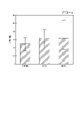
- the LPD was measured using a Surfscan SP5 manufactured by KLA-Tencor, and the number of LPDs having a size of 35 nm or more was detected and counted in the measurement mode DCN. This was performed on four silicon wafers, and the average value of the number of LPDs was calculated.
- Example 2 Same as Example 1 except that polishing was not performed after the pre-stage polishing step and before the finish polishing step, and the same polishing step as that of the pre-polishing step of Example 1 was performed after the finish polishing step. Polishing was performed by the method of.
- FIG. 3 As shown in FIG. 3, according to the first embodiment, it can be seen that the LPD could be reduced as compared with the conventional examples 1 and 2.
- 100 Single-sided polishing device, 10: Rotating surface plate, 12: Polishing pad, 14: Surface plate rotation axis, 20: Polishing head, 22: Backing pad, 24: Retaining, 26: Shaft part, 28: Rotating frame part, 30: Slurry supply unit, 32: Polishing slurry, W: Silicon wafer
Landscapes
- Engineering & Computer Science (AREA)
- Mechanical Engineering (AREA)
- Mechanical Treatment Of Semiconductor (AREA)
- Finish Polishing, Edge Sharpening, And Grinding By Specific Grinding Devices (AREA)
- Grinding-Machine Dressing And Accessory Apparatuses (AREA)
- Crystals, And After-Treatments Of Crystals (AREA)
Abstract
Description
(1)表面に第1研磨パッドを設けた第1定盤と、第1研磨ヘッドと、を含む前段研磨ユニットを用いて、前記第1研磨パッドに第1研磨液を供給しつつ、前記第1研磨ヘッドにより保持したシリコンウェーハを前記第1研磨パッドに接触させた状態で前記第1定盤及び前記シリコンウェーハを回転させることで、前記シリコンウェーハの表面を研磨する前段研磨工程と、
その後、表面に第2研磨パッドを設けた第2定盤と、第2研磨ヘッドと、を含む仕上げ研磨ユニットを用いて、前記第2研磨パッドに第2研磨液を供給しつつ、前記第2研磨ヘッドにより保持した前記シリコンウェーハを前記第2研磨パッドに接触させた状態で前記第2定盤および前記シリコンウェーハを回転させることで、前記シリコンウェーハの表面をさらに研磨する仕上げ研磨工程と、
を最終研磨工程として行うことを含む、シリコンウェーハの研磨方法であって、
前記最終研磨工程における前記仕上げ研磨工程は、
前記第2研磨液として砥粒の密度が1×10¹³個/cm3以上である研磨液を用いる、仕上げスラリー研磨工程と、
前記仕上げスラリー研磨工程に先立って行われ、前記第2研磨液として砥粒の密度が1×10¹⁰個/cm3以下である研磨液を用いる、プレ研磨工程と、を含むことを特徴とする、シリコンウェーハの研磨方法。
ここで、「前記第2研磨液として砥粒の密度が1×10¹⁰個/cm3以下である研磨液」には、純水等、砥粒を含まない研磨液も含まれる。
図1は、本発明の一実施形態にかかるシリコンウェーハの研磨方法を含む、シリコンウェーハの製造工程を示すフロー図である。図2は、本発明の一実施形態のシリコンウェーハの研磨方法における仕上げ研磨工程で用いる、片面研磨装置を示す模式図である。
仕上げ研磨工程(ステップS6)については、後に詳細に説明する。
本発明者らは、仕上げ研磨工程で用いる研磨ヘッド、特にリテーナリングの内壁にパーティクルが蓄積し、このパーティクルにより仕上げ研磨工程時にシリコンウェーハの表面に傷が発生してLPDが発生する原因となっていたことを突き止めた。
これに対し、本実施形態のシリコンウェーハの研磨方法によれば、最終研磨工程における仕上げ研磨工程(ステップS5)は、第2研磨液として砥粒の密度が1×10¹³個/cm3以上である研磨液を用いる、仕上げスラリー研磨工程(ステップS52)と、仕上げスラリー研磨工程(ステップS52)に先立って行われる、第2研磨液として砥粒の密度が1×1010個/cm3以下である研磨液を用いる、プレ研磨工程(ステップS51)と、を含む。
このように、プレ研磨工程(ステップS51)を仕上げスラリー研磨工程(ステップS52)に先立って行うことにより、仕上げ研磨の研磨ヘッド(特にリテーナリングの内壁)に付着しているパーティクルを除去することができ、パーティクルが起因となるLPDの発生を抑制することができる。
本発明の一実施形態にかかるシリコンウェーハの製造方法では、まず、チョクラルスキー法で育成した単結晶シリコンインゴットをスライスして研磨前シリコンウェーハを得る。単結晶シリコンインゴットの育成やスライス工程については、従来の手法と同様に行うことができる。
前段研磨まで終えたシリコンウェーハに対して、プレ研磨工程を行ってから、仕上げ研磨工程を行った。その後、シリコンウェーハを洗浄し、LPDを測定した。
プレ研磨工程では、研磨液として砥粒を含まない純水を用いた。研磨時間を30秒とし、研磨ヘッドの回転速度を仕上げ研磨工程での研磨ヘッドの回転速度の2倍とした。
仕上げ研磨工程では、砥粒としてSiO2を用いたアルカリ水溶液であって、砥粒の密度が5×10¹³個/cm3である、研磨スラリーを用いた。研磨時間を180秒とした。
LPDの測定は、KLA-Tencor社製、Surfscan SP5を用いて、測定モードDCNで、35nm以上のサイズのLPDを検出して個数をカウントした。これを4枚のシリコンウェーハで行い、LPD個数の平均値を算出した。
プレ研磨工程を行わなかったこと以外は、実施例1と同様の方法で研磨を行った。
前段研磨工程の後、仕上げ研磨工程の前には研磨を行わず、且つ、仕上げ研磨工程の後に、実施例1のプレ研磨工程と同様の研磨工程を行ったこと以外は、実施例1と同様の方法で研磨を行った。
10:回転定盤、
12:研磨パッド、
14:定盤回転軸、
20:研磨ヘッド、
22:バッキングパッド、
24:リテーナリング、
26:シャフト部、
28:回転フレーム部、
30:スラリー供給部、
32:研磨スラリー、
W:シリコンウェーハ
Claims (6)
- 表面に第1研磨パッドを設けた第1定盤と、第1研磨ヘッドと、を含む前段研磨ユニットを用いて、前記第1研磨パッドに第1研磨液を供給しつつ、前記第1研磨ヘッドにより保持したシリコンウェーハを前記第1研磨パッドに接触させた状態で前記第1定盤及び前記シリコンウェーハを回転させることで、前記シリコンウェーハの表面を研磨する前段研磨工程と、
その後、表面に第2研磨パッドを設けた第2定盤と、第2研磨ヘッドと、を含む仕上げ研磨ユニットを用いて、前記第2研磨パッドに第2研磨液を供給しつつ、前記第2研磨ヘッドにより保持した前記シリコンウェーハを前記第2研磨パッドに接触させた状態で前記第2定盤および前記シリコンウェーハを回転させることで、前記シリコンウェーハの表面をさらに研磨する仕上げ研磨工程と、
を最終研磨工程として行うことを含む、シリコンウェーハの研磨方法であって、
前記最終研磨工程における前記仕上げ研磨工程は、
前記第2研磨液として砥粒の密度が1×10¹³個/cm3以上である研磨液を用いる、仕上げスラリー研磨工程と、
前記仕上げスラリー研磨工程に先立って行われ、前記第2研磨液として砥粒の密度が1×10¹⁰個/cm3以下である研磨液を用いる、プレ研磨工程と、を含むことを特徴とする、シリコンウェーハの研磨方法。 - 前記プレ研磨工程において用いる前記第2研磨液は、純水である、請求項1に記載のシリコンウェーハの研磨方法。
- 前記プレ研磨工程は、10~60秒の範囲で行う、請求項1又は2に記載のシリコンウェーハの研磨方法。
- 前記プレ研磨工程における前記第2研磨ヘッドの回転数は、前記仕上げスラリー研磨工程における前記第2研磨ヘッドの回転数より大きい、請求項1~3のいずれか一項に記載のシリコンウェーハの研磨方法。
- 前記プレ研磨工程における前記第2研磨ヘッドの回転数は、前記仕上げスラリー研磨工程における前記第2研磨ヘッドの回転数の1.5倍以上である、請求項4に記載のシリコンウェーハの研磨方法。
- チョクラルスキー法で育成した単結晶シリコンインゴットをスライスして研磨前シリコンウェーハを得た後、得られた研磨前シリコンウェーハに対して、請求項1~5のいずれか一項に記載のシリコンウェーハの研磨方法により研磨処理を施すことを特徴とするシリコンウェーハの製造方法。
Priority Applications (4)
| Application Number | Priority Date | Filing Date | Title |
|---|---|---|---|
| US18/257,492 US12496678B2 (en) | 2020-12-16 | 2021-08-25 | Method of polishing silicon wafer and method of producing silicon wafer |
| CN202180085438.2A CN116669902B (zh) | 2020-12-16 | 2021-08-25 | 硅晶片的抛光方法及硅晶片的制造方法 |
| DE112021006523.8T DE112021006523T5 (de) | 2020-12-16 | 2021-08-25 | Verfahren zum polieren eines siliziumwafers und verfahren zum herstellen eines siliziumwafers |
| KR1020237012030A KR102733796B1 (ko) | 2020-12-16 | 2021-08-25 | 실리콘 웨이퍼의 연마 방법 및 실리콘 웨이퍼의 제조 방법 |
Applications Claiming Priority (2)
| Application Number | Priority Date | Filing Date | Title |
|---|---|---|---|
| JP2020-208282 | 2020-12-16 | ||
| JP2020208282A JP7040591B1 (ja) | 2020-12-16 | 2020-12-16 | シリコンウェーハの研磨方法及びシリコンウェーハの製造方法 |
Publications (1)
| Publication Number | Publication Date |
|---|---|
| WO2022130696A1 true WO2022130696A1 (ja) | 2022-06-23 |
Family
ID=81214317
Family Applications (1)
| Application Number | Title | Priority Date | Filing Date |
|---|---|---|---|
| PCT/JP2021/031247 Ceased WO2022130696A1 (ja) | 2020-12-16 | 2021-08-25 | シリコンウェーハの研磨方法及びシリコンウェーハの製造方法 |
Country Status (7)
| Country | Link |
|---|---|
| US (1) | US12496678B2 (ja) |
| JP (1) | JP7040591B1 (ja) |
| KR (1) | KR102733796B1 (ja) |
| CN (1) | CN116669902B (ja) |
| DE (1) | DE112021006523T5 (ja) |
| TW (1) | TWI775622B (ja) |
| WO (1) | WO2022130696A1 (ja) |
Citations (4)
| Publication number | Priority date | Publication date | Assignee | Title |
|---|---|---|---|---|
| JP2003311593A (ja) * | 2002-02-20 | 2003-11-05 | Ebara Corp | ポリッシング装置 |
| WO2012002525A1 (ja) * | 2010-07-02 | 2012-01-05 | 株式会社Sumco | シリコンウェーハの研磨方法 |
| JP2015159259A (ja) * | 2014-02-25 | 2015-09-03 | 株式会社フジミインコーポレーテッド | 半導体基板を連続的に製造する方法 |
| JP2017183478A (ja) * | 2016-03-30 | 2017-10-05 | 株式会社フジミインコーポレーテッド | シリコンウェーハの研磨方法及び研磨用組成物セット |
Family Cites Families (16)
| Publication number | Priority date | Publication date | Assignee | Title |
|---|---|---|---|---|
| JP3086437B2 (ja) * | 1997-12-15 | 2000-09-11 | 松下電器産業株式会社 | 化学的機械研磨装置及び化学的機械研磨方法 |
| JP3551226B2 (ja) | 1998-02-26 | 2004-08-04 | 三菱住友シリコン株式会社 | 半導体基板の研磨終了時のリンス液及びこれを用いたリンス法 |
| JP3737021B2 (ja) * | 2000-07-27 | 2006-01-18 | 信越半導体株式会社 | シリコンエピタキシャルウェーハの製造方法 |
| KR20030056674A (ko) * | 2001-12-28 | 2003-07-04 | 삼성전자주식회사 | 연마 설비의 클리닝 장치 |
| JP4268402B2 (ja) * | 2002-12-02 | 2009-05-27 | 花王株式会社 | メモリーハードディスク基板の製造方法 |
| JP2004273502A (ja) * | 2003-03-05 | 2004-09-30 | Matsushita Electric Ind Co Ltd | ウェハの研磨方法及びその装置 |
| JP2007103703A (ja) | 2005-10-05 | 2007-04-19 | Sumco Techxiv株式会社 | 半導体ウェハの研磨方法 |
| KR100880108B1 (ko) * | 2007-09-18 | 2009-01-21 | 주식회사 실트론 | 반도체 웨이퍼 연마방법 및 이를 위한 반도체 웨이퍼연마장치 |
| WO2010140671A1 (ja) * | 2009-06-05 | 2010-12-09 | 株式会社Sumco | シリコンウェーハの研磨方法及びシリコンウェーハ |
| JP2013034026A (ja) * | 2012-11-14 | 2013-02-14 | Fujimi Inc | 研磨用組成物及びそれを用いた半導体ウエハの製造方法 |
| JP6705757B2 (ja) | 2015-02-12 | 2020-06-03 | 株式会社フジミインコーポレーテッド | シリコンウェーハの研磨方法および表面処理組成物 |
| JP6690606B2 (ja) | 2017-07-14 | 2020-04-28 | 信越半導体株式会社 | 研磨方法 |
| JP6747599B2 (ja) * | 2017-08-31 | 2020-08-26 | 株式会社Sumco | シリコンウェーハの両面研磨方法 |
| CN110800085B (zh) | 2017-10-17 | 2023-08-15 | 胜高股份有限公司 | 硅晶圆的抛光方法 |
| JP6841217B2 (ja) | 2017-12-19 | 2021-03-10 | 株式会社Sumco | インゴットブロックの製造方法、半導体ウェーハの製造方法、およびインゴットブロックの製造装置 |
| CN108581639A (zh) * | 2018-03-23 | 2018-09-28 | 上海华虹宏力半导体制造有限公司 | 一种cmp工艺的控制方法及其控制系统 |
-
2020
- 2020-12-16 JP JP2020208282A patent/JP7040591B1/ja active Active
-
2021
- 2021-08-25 WO PCT/JP2021/031247 patent/WO2022130696A1/ja not_active Ceased
- 2021-08-25 DE DE112021006523.8T patent/DE112021006523T5/de active Pending
- 2021-08-25 KR KR1020237012030A patent/KR102733796B1/ko active Active
- 2021-08-25 US US18/257,492 patent/US12496678B2/en active Active
- 2021-08-25 CN CN202180085438.2A patent/CN116669902B/zh active Active
- 2021-09-29 TW TW110136169A patent/TWI775622B/zh active
Patent Citations (4)
| Publication number | Priority date | Publication date | Assignee | Title |
|---|---|---|---|---|
| JP2003311593A (ja) * | 2002-02-20 | 2003-11-05 | Ebara Corp | ポリッシング装置 |
| WO2012002525A1 (ja) * | 2010-07-02 | 2012-01-05 | 株式会社Sumco | シリコンウェーハの研磨方法 |
| JP2015159259A (ja) * | 2014-02-25 | 2015-09-03 | 株式会社フジミインコーポレーテッド | 半導体基板を連続的に製造する方法 |
| JP2017183478A (ja) * | 2016-03-30 | 2017-10-05 | 株式会社フジミインコーポレーテッド | シリコンウェーハの研磨方法及び研磨用組成物セット |
Also Published As
| Publication number | Publication date |
|---|---|
| CN116669902B (zh) | 2026-04-28 |
| DE112021006523T5 (de) | 2023-11-16 |
| CN116669902A (zh) | 2023-08-29 |
| KR102733796B1 (ko) | 2024-11-25 |
| TW202228914A (zh) | 2022-08-01 |
| TWI775622B (zh) | 2022-08-21 |
| JP7040591B1 (ja) | 2022-03-23 |
| KR20230062646A (ko) | 2023-05-09 |
| US12496678B2 (en) | 2025-12-16 |
| JP2022095132A (ja) | 2022-06-28 |
| US20240025008A1 (en) | 2024-01-25 |
Similar Documents
| Publication | Publication Date | Title |
|---|---|---|
| US7507146B2 (en) | Method for producing semiconductor wafer and semiconductor wafer | |
| TWI742304B (zh) | 矽晶圓的研磨方法 | |
| TWI659800B (zh) | 矽晶圓之研磨方法以及矽晶圓之製造方法 | |
| JPH09270400A (ja) | 半導体ウェーハの製造方法 | |
| JP5493956B2 (ja) | 半導体ウェーハの製造方法 | |
| JPH07314324A (ja) | 表面粗さを減少させるための半導体ウエハの粗研磨法 | |
| CN104350583A (zh) | 半导体晶片的制造方法 | |
| KR20000017512A (ko) | 웨이퍼 기판 재생방법 및 웨이퍼 기판 재생을 위한 연마액 조성물 | |
| CN107155368A (zh) | 硅晶圆的研磨方法 | |
| JP2006100799A (ja) | シリコンウェーハの製造方法 | |
| KR20020023131A (ko) | 실리콘웨이퍼의 연마방법 | |
| US20010039101A1 (en) | Method for converting a reclaim wafer into a semiconductor wafer | |
| JP2007204286A (ja) | エピタキシャルウェーハの製造方法 | |
| JP7040591B1 (ja) | シリコンウェーハの研磨方法及びシリコンウェーハの製造方法 | |
| CN111615741A (zh) | 硅晶圆的制造方法 | |
| JP2003142434A (ja) | 鏡面ウエーハの製造方法 | |
| JP4683233B2 (ja) | 半導体ウェーハの製造方法 | |
| JP2007027488A (ja) | 半導体ウェーハの研磨方法 | |
| JP2003133264A (ja) | 鏡面ウエーハの製造方法 | |
| JP2005135936A (ja) | ウエーハの面取り加工方法及びウエーハ | |
| JP2003109990A (ja) | 半導体ウェーハの平坦度評価方法 | |
| JP2003218066A (ja) | 半導体ウェーハの研磨方法 |
Legal Events
| Date | Code | Title | Description |
|---|---|---|---|
| 121 | Ep: the epo has been informed by wipo that ep was designated in this application |
Ref document number: 21906061 Country of ref document: EP Kind code of ref document: A1 |
|
| ENP | Entry into the national phase |
Ref document number: 20237012030 Country of ref document: KR Kind code of ref document: A |
|
| WWE | Wipo information: entry into national phase |
Ref document number: 18257492 Country of ref document: US |
|
| WWE | Wipo information: entry into national phase |
Ref document number: 202180085438.2 Country of ref document: CN |
|
| WWE | Wipo information: entry into national phase |
Ref document number: 112021006523 Country of ref document: DE |
|
| 122 | Ep: pct application non-entry in european phase |
Ref document number: 21906061 Country of ref document: EP Kind code of ref document: A1 |
|
| WWG | Wipo information: grant in national office |
Ref document number: 18257492 Country of ref document: US |