WO2022124019A1 - フォトディテクタ、フォトディテクタアレイおよび距離測定システム - Google Patents
フォトディテクタ、フォトディテクタアレイおよび距離測定システム Download PDFInfo
- Publication number
- WO2022124019A1 WO2022124019A1 PCT/JP2021/041947 JP2021041947W WO2022124019A1 WO 2022124019 A1 WO2022124019 A1 WO 2022124019A1 JP 2021041947 W JP2021041947 W JP 2021041947W WO 2022124019 A1 WO2022124019 A1 WO 2022124019A1
- Authority
- WO
- WIPO (PCT)
- Prior art keywords
- spad
- transistor
- photodetector
- resistance
- resistor
- Prior art date
Links
- 238000005259 measurement Methods 0.000 title claims description 31
- 239000004065 semiconductor Substances 0.000 claims description 63
- 230000015556 catabolic process Effects 0.000 claims description 20
- 239000000758 substrate Substances 0.000 claims description 16
- 238000012545 processing Methods 0.000 claims description 12
- 230000003071 parasitic effect Effects 0.000 claims description 11
- 230000005684 electric field Effects 0.000 claims description 9
- 230000002093 peripheral effect Effects 0.000 claims description 5
- 238000010791 quenching Methods 0.000 description 55
- 230000000171 quenching effect Effects 0.000 description 55
- 238000010586 diagram Methods 0.000 description 42
- 238000004088 simulation Methods 0.000 description 18
- 108091006146 Channels Proteins 0.000 description 14
- 239000000463 material Substances 0.000 description 8
- 238000001514 detection method Methods 0.000 description 7
- 239000012535 impurity Substances 0.000 description 6
- 230000035945 sensitivity Effects 0.000 description 6
- 238000000034 method Methods 0.000 description 5
- 230000007423 decrease Effects 0.000 description 4
- 238000009792 diffusion process Methods 0.000 description 3
- 230000014509 gene expression Effects 0.000 description 3
- 238000004364 calculation method Methods 0.000 description 2
- 229910052710 silicon Inorganic materials 0.000 description 2
- 239000010703 silicon Substances 0.000 description 2
- JBRZTFJDHDCESZ-UHFFFAOYSA-N AsGa Chemical compound [As]#[Ga] JBRZTFJDHDCESZ-UHFFFAOYSA-N 0.000 description 1
- 229910002601 GaN Inorganic materials 0.000 description 1
- 229910001218 Gallium arsenide Inorganic materials 0.000 description 1
- JMASRVWKEDWRBT-UHFFFAOYSA-N Gallium nitride Chemical compound [Ga]#N JMASRVWKEDWRBT-UHFFFAOYSA-N 0.000 description 1
- GPXJNWSHGFTCBW-UHFFFAOYSA-N Indium phosphide Chemical compound [In]#P GPXJNWSHGFTCBW-UHFFFAOYSA-N 0.000 description 1
- 108010075750 P-Type Calcium Channels Proteins 0.000 description 1
- 206010034960 Photophobia Diseases 0.000 description 1
- BUGBHKTXTAQXES-UHFFFAOYSA-N Selenium Chemical compound [Se] BUGBHKTXTAQXES-UHFFFAOYSA-N 0.000 description 1
- 230000003321 amplification Effects 0.000 description 1
- 238000004458 analytical method Methods 0.000 description 1
- 238000013459 approach Methods 0.000 description 1
- 239000000969 carrier Substances 0.000 description 1
- 238000006243 chemical reaction Methods 0.000 description 1
- 238000004891 communication Methods 0.000 description 1
- 230000003247 decreasing effect Effects 0.000 description 1
- 230000007547 defect Effects 0.000 description 1
- 239000007772 electrode material Substances 0.000 description 1
- 229910052732 germanium Inorganic materials 0.000 description 1
- GNPVGFCGXDBREM-UHFFFAOYSA-N germanium atom Chemical compound [Ge] GNPVGFCGXDBREM-UHFFFAOYSA-N 0.000 description 1
- 229910052737 gold Inorganic materials 0.000 description 1
- 238000003384 imaging method Methods 0.000 description 1
- AMGQUBHHOARCQH-UHFFFAOYSA-N indium;oxotin Chemical compound [In].[Sn]=O AMGQUBHHOARCQH-UHFFFAOYSA-N 0.000 description 1
- 239000007924 injection Substances 0.000 description 1
- 238000002347 injection Methods 0.000 description 1
- 230000031700 light absorption Effects 0.000 description 1
- 208000013469 light sensitivity Diseases 0.000 description 1
- 239000004973 liquid crystal related substance Substances 0.000 description 1
- 238000012986 modification Methods 0.000 description 1
- 230000004048 modification Effects 0.000 description 1
- 238000003199 nucleic acid amplification method Methods 0.000 description 1
- 230000003287 optical effect Effects 0.000 description 1
- 229910052697 platinum Inorganic materials 0.000 description 1
- 230000005855 radiation Effects 0.000 description 1
- 229910052711 selenium Inorganic materials 0.000 description 1
- 239000011669 selenium Substances 0.000 description 1
- 238000000926 separation method Methods 0.000 description 1
- 229910052709 silver Inorganic materials 0.000 description 1
- 229910052719 titanium Inorganic materials 0.000 description 1
- 238000002834 transmittance Methods 0.000 description 1
Images


Classifications
-
- H—ELECTRICITY
- H01—ELECTRIC ELEMENTS
- H01L—SEMICONDUCTOR DEVICES NOT COVERED BY CLASS H10
- H01L27/00—Devices consisting of a plurality of semiconductor or other solid-state components formed in or on a common substrate
- H01L27/14—Devices consisting of a plurality of semiconductor or other solid-state components formed in or on a common substrate including semiconductor components sensitive to infrared radiation, light, electromagnetic radiation of shorter wavelength or corpuscular radiation and specially adapted either for the conversion of the energy of such radiation into electrical energy or for the control of electrical energy by such radiation
- H01L27/144—Devices controlled by radiation
- H01L27/146—Imager structures
- H01L27/14643—Photodiode arrays; MOS imagers
- H01L27/14645—Colour imagers
-
- G—PHYSICS
- G01—MEASURING; TESTING
- G01S—RADIO DIRECTION-FINDING; RADIO NAVIGATION; DETERMINING DISTANCE OR VELOCITY BY USE OF RADIO WAVES; LOCATING OR PRESENCE-DETECTING BY USE OF THE REFLECTION OR RERADIATION OF RADIO WAVES; ANALOGOUS ARRANGEMENTS USING OTHER WAVES
- G01S17/00—Systems using the reflection or reradiation of electromagnetic waves other than radio waves, e.g. lidar systems
- G01S17/02—Systems using the reflection of electromagnetic waves other than radio waves
- G01S17/06—Systems determining position data of a target
- G01S17/08—Systems determining position data of a target for measuring distance only
- G01S17/10—Systems determining position data of a target for measuring distance only using transmission of interrupted, pulse-modulated waves
-
- G—PHYSICS
- G01—MEASURING; TESTING
- G01S—RADIO DIRECTION-FINDING; RADIO NAVIGATION; DETERMINING DISTANCE OR VELOCITY BY USE OF RADIO WAVES; LOCATING OR PRESENCE-DETECTING BY USE OF THE REFLECTION OR RERADIATION OF RADIO WAVES; ANALOGOUS ARRANGEMENTS USING OTHER WAVES
- G01S7/00—Details of systems according to groups G01S13/00, G01S15/00, G01S17/00
- G01S7/48—Details of systems according to groups G01S13/00, G01S15/00, G01S17/00 of systems according to group G01S17/00
- G01S7/481—Constructional features, e.g. arrangements of optical elements
- G01S7/4816—Constructional features, e.g. arrangements of optical elements of receivers alone
-
- G—PHYSICS
- G01—MEASURING; TESTING
- G01S—RADIO DIRECTION-FINDING; RADIO NAVIGATION; DETERMINING DISTANCE OR VELOCITY BY USE OF RADIO WAVES; LOCATING OR PRESENCE-DETECTING BY USE OF THE REFLECTION OR RERADIATION OF RADIO WAVES; ANALOGOUS ARRANGEMENTS USING OTHER WAVES
- G01S7/00—Details of systems according to groups G01S13/00, G01S15/00, G01S17/00
- G01S7/48—Details of systems according to groups G01S13/00, G01S15/00, G01S17/00 of systems according to group G01S17/00
- G01S7/483—Details of pulse systems
- G01S7/486—Receivers
- G01S7/4861—Circuits for detection, sampling, integration or read-out
- G01S7/4863—Detector arrays, e.g. charge-transfer gates
-
- H—ELECTRICITY
- H01—ELECTRIC ELEMENTS
- H01L—SEMICONDUCTOR DEVICES NOT COVERED BY CLASS H10
- H01L27/00—Devices consisting of a plurality of semiconductor or other solid-state components formed in or on a common substrate
- H01L27/14—Devices consisting of a plurality of semiconductor or other solid-state components formed in or on a common substrate including semiconductor components sensitive to infrared radiation, light, electromagnetic radiation of shorter wavelength or corpuscular radiation and specially adapted either for the conversion of the energy of such radiation into electrical energy or for the control of electrical energy by such radiation
- H01L27/144—Devices controlled by radiation
- H01L27/1443—Devices controlled by radiation with at least one potential jump or surface barrier
-
- H—ELECTRICITY
- H01—ELECTRIC ELEMENTS
- H01L—SEMICONDUCTOR DEVICES NOT COVERED BY CLASS H10
- H01L27/00—Devices consisting of a plurality of semiconductor or other solid-state components formed in or on a common substrate
- H01L27/14—Devices consisting of a plurality of semiconductor or other solid-state components formed in or on a common substrate including semiconductor components sensitive to infrared radiation, light, electromagnetic radiation of shorter wavelength or corpuscular radiation and specially adapted either for the conversion of the energy of such radiation into electrical energy or for the control of electrical energy by such radiation
- H01L27/144—Devices controlled by radiation
- H01L27/1446—Devices controlled by radiation in a repetitive configuration
-
- H—ELECTRICITY
- H01—ELECTRIC ELEMENTS
- H01L—SEMICONDUCTOR DEVICES NOT COVERED BY CLASS H10
- H01L27/00—Devices consisting of a plurality of semiconductor or other solid-state components formed in or on a common substrate
- H01L27/14—Devices consisting of a plurality of semiconductor or other solid-state components formed in or on a common substrate including semiconductor components sensitive to infrared radiation, light, electromagnetic radiation of shorter wavelength or corpuscular radiation and specially adapted either for the conversion of the energy of such radiation into electrical energy or for the control of electrical energy by such radiation
- H01L27/144—Devices controlled by radiation
- H01L27/146—Imager structures
- H01L27/14601—Structural or functional details thereof
- H01L27/14609—Pixel-elements with integrated switching, control, storage or amplification elements
- H01L27/14612—Pixel-elements with integrated switching, control, storage or amplification elements involving a transistor
- H01L27/14616—Pixel-elements with integrated switching, control, storage or amplification elements involving a transistor characterised by the channel of the transistor, e.g. channel having a doping gradient
-
- H—ELECTRICITY
- H01—ELECTRIC ELEMENTS
- H01L—SEMICONDUCTOR DEVICES NOT COVERED BY CLASS H10
- H01L27/00—Devices consisting of a plurality of semiconductor or other solid-state components formed in or on a common substrate
- H01L27/14—Devices consisting of a plurality of semiconductor or other solid-state components formed in or on a common substrate including semiconductor components sensitive to infrared radiation, light, electromagnetic radiation of shorter wavelength or corpuscular radiation and specially adapted either for the conversion of the energy of such radiation into electrical energy or for the control of electrical energy by such radiation
- H01L27/144—Devices controlled by radiation
- H01L27/146—Imager structures
- H01L27/14601—Structural or functional details thereof
- H01L27/14636—Interconnect structures
-
- H—ELECTRICITY
- H01—ELECTRIC ELEMENTS
- H01L—SEMICONDUCTOR DEVICES NOT COVERED BY CLASS H10
- H01L31/00—Semiconductor devices sensitive to infrared radiation, light, electromagnetic radiation of shorter wavelength or corpuscular radiation and specially adapted either for the conversion of the energy of such radiation into electrical energy or for the control of electrical energy by such radiation; Processes or apparatus specially adapted for the manufacture or treatment thereof or of parts thereof; Details thereof
- H01L31/08—Semiconductor devices sensitive to infrared radiation, light, electromagnetic radiation of shorter wavelength or corpuscular radiation and specially adapted either for the conversion of the energy of such radiation into electrical energy or for the control of electrical energy by such radiation; Processes or apparatus specially adapted for the manufacture or treatment thereof or of parts thereof; Details thereof in which radiation controls flow of current through the device, e.g. photoresistors
- H01L31/10—Semiconductor devices sensitive to infrared radiation, light, electromagnetic radiation of shorter wavelength or corpuscular radiation and specially adapted either for the conversion of the energy of such radiation into electrical energy or for the control of electrical energy by such radiation; Processes or apparatus specially adapted for the manufacture or treatment thereof or of parts thereof; Details thereof in which radiation controls flow of current through the device, e.g. photoresistors characterised by at least one potential-jump barrier or surface barrier, e.g. phototransistors
- H01L31/101—Devices sensitive to infrared, visible or ultraviolet radiation
- H01L31/102—Devices sensitive to infrared, visible or ultraviolet radiation characterised by only one potential barrier or surface barrier
- H01L31/107—Devices sensitive to infrared, visible or ultraviolet radiation characterised by only one potential barrier or surface barrier the potential barrier working in avalanche mode, e.g. avalanche photodiode
-
- G—PHYSICS
- G01—MEASURING; TESTING
- G01S—RADIO DIRECTION-FINDING; RADIO NAVIGATION; DETERMINING DISTANCE OR VELOCITY BY USE OF RADIO WAVES; LOCATING OR PRESENCE-DETECTING BY USE OF THE REFLECTION OR RERADIATION OF RADIO WAVES; ANALOGOUS ARRANGEMENTS USING OTHER WAVES
- G01S17/00—Systems using the reflection or reradiation of electromagnetic waves other than radio waves, e.g. lidar systems
- G01S17/88—Lidar systems specially adapted for specific applications
- G01S17/89—Lidar systems specially adapted for specific applications for mapping or imaging
- G01S17/894—3D imaging with simultaneous measurement of time-of-flight at a 2D array of receiver pixels, e.g. time-of-flight cameras or flash lidar
Abstract
Description
本発明者は、「背景技術」の欄において記載した、SPAD(Single Photon Avalanche Diode)に関し、以下の問題が生じることを見出した。
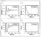
まず、本開示の基になったシミュレーションについて説明する。


となる。ただし、
はアバランシェ増倍による電圧変動の時定数であり、T0はn(t)が最小となる時間である。


但し、

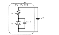
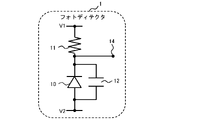
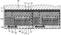
図4~7を用いて実施の形態1に係るフォトディテクタ1について説明する。
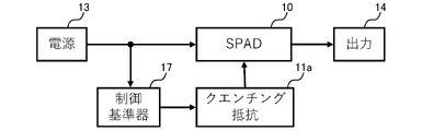
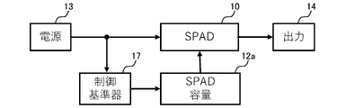
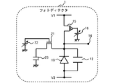
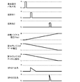
図8は実施の形態2に係るフォトディテクタ1を含む制御システムの構成例を示すブロック図である。この制御システムは、電源13とSPAD10とクエンチング抵抗11aと制御基準器17と、出力部14とを備える。SPAD10およびクエンチング抵抗11aは、図5のフォトディテクタ1に相当する。例えば、クエンチング抵抗11aは、図5の第1トランジスタ15および第1可変電源16に相当する。第1可変電源16は、制御基準器17の制御に従って可変の電圧を第1トランジスタ15のゲートに出力する。
図11は実施の形態3に係るフォトディテクタアレイの回路例を示す図である。このフォトディテクタアレイは、N個(Nは2以上の自然数)のフォトディテクタ1を並列に備え、さらに第2抵抗24を備える。N個のフォトディテクタ1のそれぞれは、SPAD10と、第1トランジスタ15と、第1可変電源16を備える。フォトディテクタ1が接続された端、すなわち、SPAD10が接続された端には、SPAD10と第2電源V2の間に第2抵抗24が接続される。この時、第2抵抗24は、N個のSPAD10すべてで発生した電荷を、SPAD10のリチャージ時間より短時間で排出することが要求される。すなわち、第2抵抗24の抵抗値rによる時定数rNCが第1抵抗11の抵抗値RによるSPAD10のリチャージ時間RCより短いことが求められる。すなわち、下記の式を満たすことが要求される。

以下、フォトディテクタあるいはフォトディテクタアレイの応用例について図面を参照しながら説明する。
10 SPAD
11 第1抵抗
11a クエンチング抵抗
12 第1容量
12a SPAD容量
13 電源
14 出力部
15、15a 第1トランジスタ
16、16a 第1可変電源
17 制御基準器
21 第2トランジスタ
22 第2可変電源
23 第2容量
24 第2抵抗
31 第3抵抗
32 第3容量
33 第3トランジスタ
34 第4トランジスタ
35 第5トランジスタ
36 第6トランジスタ
37 第4容量
41 選択部
42 制御基準器
43 負荷部
44 信号処理部
45 出力部
46 受光領域
47 コンタクト領域
48 半導体チップ
100 固体撮像装置
500 測距測定システム
510 発光部
520 受光部
530 制御部
540 出力部
CA コンタクト領域
EL 電極
FL フィルタ
G1、G2、G3 ゲート
L1 第1半導体層
L2 第2半導体層
L3 第3半導体層
L4 第4半導体層
L5 第5半導体層
LL レンズ層
LM 配線層
ML マイクロレンズ
MP 増倍領域
S1 第1主面
S2 第2主面
SUB 半導体基板
V1 第1電源
V2 第2電源
W1 第1配線
W2 第2配線
WL1 第1ウェル
Claims (21)
- シングルフォトンアバランシェダイオード(以下、SPADと記す)と、
前記SPADに直列に接続された第1抵抗とを備え、
前記SPADから前記第1抵抗を介して電荷が排出されるリチャージ時間において、前記SPADの増倍領域から電荷が無くなる
フォトディテクタ。 - 前記SPADの端のうち、前記第1抵抗と接続された端の電圧振幅の最大値は、前記SPADの両端に印加される電圧と前記SPADのブレークダウン電圧との差分である余剰電圧よりも大きい
請求項1に記載のフォトディテクタ。 - シングルフォトンアバランシェダイオード(以下、SPADと記す)と、
前記SPADと並列に接続された容量と、
前記SPADに直列に接続された第1抵抗と、
前記SPADの端のうち、前記第1抵抗と接続された端の電圧を読み出す読み出し部を備える、
フォトディテクタ。 - 前記SPADに印加される余剰バイアス電圧は、前記SPADのブレークダウン電圧より小さく、
前記第1抵抗の抵抗値Rは

式中のEBDは、前記SPAD内部の電界強度を、
Cは、SPADの寄生容量を含む容量を、
Vexは、前記余剰バイアス電圧であって、前記SPADに印加される逆バイアス電圧と前記ブレークダウン電圧との差分を、
Wは、前記SPADの空乏層幅を、
α(EBD)は、電界強度EBDの下での電子のインパクトイオン化率を、
β(EBD)は、電界強度EBDの下での正孔のインパクトイオン化率を、
aは、電子のインパクトイオン化率の係数を、
bは、正孔のインパクトイオン化率の係数を、
qは、電気素量を、
vs,eは、電子の飽和速度を示す、
請求項1または3に記載のフォトディテクタ。 - 制御基準器を備え、
前記制御基準器は次の5つのパラメータ
(i)前記第1抵抗の抵抗値R、
(ii)前記SPADの寄生容量を含むC、
(iii)前記SPADの両端に印加される電圧と前記SPADのブレークダウン電圧との差分である余剰バイアス電圧Vex、
(iv)前記SPADの空乏層幅W、
(v)前記ブレークダウン電圧のいずれか1以上を参照し、前記参照したパラメータ以外の1以上のパラメータを制御する、
請求項2または3に記載のフォトディテクタ。 - 前記第1抵抗は可変抵抗であり、
前記制御基準器は、前記余剰バイアス電圧が大きいほど、前記第1抵抗の抵抗値を小さくする、
請求項5に記載のフォトディテクタ。 - 前記第1抵抗は第1トランジスタを含み、
前記第1抵抗の抵抗値は、前記第1トランジスタのチャネル抵抗に対応する、
請求項6に記載のフォトディテクタ。 - 前記SPADの寄生容量を含む容量Cは可変であり、
前記制御基準器は、前記余剰バイアス電圧が大きいほど、容量Cの容量値を小さくする、
請求項5に記載のフォトディテクタ。 - 前記第1抵抗は第1トランジスタを含み、
前記SPADと前記第1トランジスタの接続された端に第2トランジスタを備え、
前記第2トランジスタの前記接続された端と逆の端には、第2容量を備え、
前記SPADの余剰バイアス電圧を参照し、前記第2トランジスタのゲート電圧を制御する、
請求項8に記載のフォトディテクタ。 - 請求項1~9のいずれか1項に記載のフォトディテクタをN個備え(Nは2以上の整数)、
前記N個のフォトディテクタに含まれるN個の直列回路は並列に接続され、
前記N個の直列回路のそれぞれは、直列接続された前記SPADおよび前記第1抵抗を有し、
前記N個の直列回路の一端であって前記SPAD側のN個の一端は互いに接続され、
さらに、前記互いに接続されたN個の前記一端に接続され、かつ、前記N個のフォトディテクタと直列に接続される第2抵抗を備え、
前記第2抵抗の抵抗値は、前記第1抵抗の抵抗値のN分の1よりも小さい、
フォトディテクタアレイ。 - 前記N個のSPADは、同一の半導体基板上に配置され、
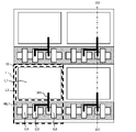
前記互いに接続されたN個の前記一端は、前記半導体基板を介して接続される、
請求項10に記載のフォトディテクタアレイ。 - 前記半導体基板の主面であり、前記互いに接続されたN個の前記一端の側の主面である第2主面に接して配置された電極を介して、
前記互いに接続されたN個の一端に電圧が印加される、
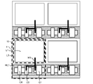
請求項11に記載のフォトディテクタアレイ。 - 前記N個のフォトディテクタの配された受光領域と、
前記受光領域の外に配されたコンタクト領域と、
前記コンタクト領域に、前記半導体基板の主面であり、前記互いに接続されたN個の前記一端の側の主面である第2主面と逆側の主面である第1主面に接するように配された第2配線と、を備え、
前記互いに接続されたN個の前記一端には前記第2配線を介して電圧が印加される、
請求項11に記載のフォトディテクタアレイ。 - 前記N個のフォトディテクタの制御、または信号処理を行う周辺回路部を備え、
前記コンタクト領域は、前記受光領域と前記周辺回路部の間に配置される、
請求項13に記載のフォトディテクタアレイ。 - 前記第1抵抗は第1トランジスタを含み、
前記N個のフォトディテクタのそれぞれは、前記第1トランジスタを含む少なくとも2つのトランジスタを備え、
前記第1抵抗は前記第1トランジスタのチャネル抵抗であり、
前記第1トランジスタのゲート面積は前記フォトディテクタの有する他のトランジスタのゲート面積より大きい、
請求項10~14のいずれか1項に記載のフォトディテクタアレイ。 - 請求項1に記載のフォトディテクタをM個(Mは2以上の整数)備え、
前記フォトディテクタ同士は、前記SPADの一方の端で接続され、
前記接続された端に第3抵抗および、第3容量が接続され、
前記第1抵抗は第1トランジスタを含み、
前記第1抵抗は前記第1トランジスタであり、
第3抵抗の抵抗値r’は

請求項4~9または15のいずれか1項に記載のフォトディテクタアレイ。 - 前記第1トランジスタは、
前記SPADをリセットするリセット期間において導通状態であり、
前記SPADに入射した光を検出する露光期間において非導通状態である、
請求項16に記載のフォトディテクタアレイ。 - 前記第1トランジスタのチャネルの導電型は、
前記SPADの、前記第1トランジスタが接続された端の導電型と同一である、
請求項16または17に記載のフォトディテクタアレイ。 - 前記第3容量の容量値は、前記SPADの容量より大きい
請求項16~18のいずれか1項に記載のフォトディテクタアレイ。 - 請求項1~15のいずれか一項に記載のフォトディテクタを有する受光部と、
測定対象物に向けて発光する発光部と、
前記受光部および前記発光部を制御する制御部と、を備え、
前記制御部は、前記測定対象物で反射した反射光に対応する信号を前記受光部から受け、前記測定対象物までの距離を算出する、
距離測定システム。 - 前記第1抵抗は第1トランジスタを含み、
前記発光部の発光後に、前記SPADの両端に印加される電圧と前記SPADのブレークダウン電圧との差分である余剰バイアス電圧を時間と共に増大させ、
前記第1トランジスタのチャネル抵抗を時間と共に低下させる、
請求項20に記載の距離測定システム。
Priority Applications (3)
| Application Number | Priority Date | Filing Date | Title |
|---|---|---|---|
| CN202180081353.7A CN116547821A (zh) | 2020-12-10 | 2021-11-15 | 光电检测器、光电检测器阵列及距离测量系统 |
| JP2022568139A JPWO2022124019A1 (ja) | 2020-12-10 | 2021-11-15 | |
| US18/325,709 US20230299114A1 (en) | 2020-12-10 | 2023-05-30 | Photodetector, photodetector array, and distance measurement system |
Applications Claiming Priority (2)
| Application Number | Priority Date | Filing Date | Title |
|---|---|---|---|
| JP2020-205037 | 2020-12-10 | ||
| JP2020205037 | 2020-12-10 |
Related Child Applications (1)
| Application Number | Title | Priority Date | Filing Date |
|---|---|---|---|
| US18/325,709 Continuation US20230299114A1 (en) | 2020-12-10 | 2023-05-30 | Photodetector, photodetector array, and distance measurement system |
Publications (1)
| Publication Number | Publication Date |
|---|---|
| WO2022124019A1 true WO2022124019A1 (ja) | 2022-06-16 |
Family
ID=81972961
Family Applications (1)
| Application Number | Title | Priority Date | Filing Date |
|---|---|---|---|
| PCT/JP2021/041947 WO2022124019A1 (ja) | 2020-12-10 | 2021-11-15 | フォトディテクタ、フォトディテクタアレイおよび距離測定システム |
Country Status (4)
| Country | Link |
|---|---|
| US (1) | US20230299114A1 (ja) |
| JP (1) | JPWO2022124019A1 (ja) |
| CN (1) | CN116547821A (ja) |
| WO (1) | WO2022124019A1 (ja) |
Citations (4)
| Publication number | Priority date | Publication date | Assignee | Title |
|---|---|---|---|---|
| JP2018179732A (ja) * | 2017-04-12 | 2018-11-15 | 株式会社デンソー | 光検出器 |
| US10312274B1 (en) * | 2018-01-29 | 2019-06-04 | Stmicroelectronics (Research & Development) Limited | Single photon avalanche diode (SPAD) with variable quench resistor |
| JP2019190892A (ja) * | 2018-04-20 | 2019-10-31 | ソニーセミコンダクタソリューションズ株式会社 | 受光装置及び測距装置 |
| WO2020179696A1 (ja) * | 2019-03-07 | 2020-09-10 | ソニーセミコンダクタソリューションズ株式会社 | 受光装置および測距装置 |
-
2021
- 2021-11-15 CN CN202180081353.7A patent/CN116547821A/zh active Pending
- 2021-11-15 WO PCT/JP2021/041947 patent/WO2022124019A1/ja active Application Filing
- 2021-11-15 JP JP2022568139A patent/JPWO2022124019A1/ja active Pending
-
2023
- 2023-05-30 US US18/325,709 patent/US20230299114A1/en active Pending
Patent Citations (4)
| Publication number | Priority date | Publication date | Assignee | Title |
|---|---|---|---|---|
| JP2018179732A (ja) * | 2017-04-12 | 2018-11-15 | 株式会社デンソー | 光検出器 |
| US10312274B1 (en) * | 2018-01-29 | 2019-06-04 | Stmicroelectronics (Research & Development) Limited | Single photon avalanche diode (SPAD) with variable quench resistor |
| JP2019190892A (ja) * | 2018-04-20 | 2019-10-31 | ソニーセミコンダクタソリューションズ株式会社 | 受光装置及び測距装置 |
| WO2020179696A1 (ja) * | 2019-03-07 | 2020-09-10 | ソニーセミコンダクタソリューションズ株式会社 | 受光装置および測距装置 |
Also Published As
| Publication number | Publication date |
|---|---|
| CN116547821A (zh) | 2023-08-04 |
| US20230299114A1 (en) | 2023-09-21 |
| JPWO2022124019A1 (ja) | 2022-06-16 |
Similar Documents
| Publication | Publication Date | Title |
|---|---|---|
| CN111682039B (zh) | 堆叠式背面照明spad阵列 | |
| RU2686396C2 (ru) | Устройство фотодетектирования и система фотодетектирования | |
| JP6696695B2 (ja) | 光検出装置およびこれを用いた被写体検知システム | |
| KR20170017803A (ko) | 광전 변환 디바이스, 거리 측정 장치 및 정보 처리 시스템 | |
| US11791433B2 (en) | Single photon avalanche diode | |
| US20220005854A1 (en) | Photodetector | |
| JP2019169643A (ja) | 固体撮像素子 | |
| WO2022070655A1 (ja) | フォトディテクタ、フォトディテクタアレイおよび駆動方法 | |
| JP2018006989A (ja) | 光学装置およびシステム | |
| WO2022124019A1 (ja) | フォトディテクタ、フォトディテクタアレイおよび距離測定システム | |
| JP2006041189A (ja) | 固体撮像素子 | |
| US20170160406A1 (en) | Photodetector, and ct device including said photodetector | |
| US20230011366A1 (en) | Semiconductor device and electronic apparatus | |
| JP2012194198A (ja) | 光センサおよび表示装置 | |
| WO2022202451A1 (ja) | 光検出器および距離測定システム | |
| JP2017037937A (ja) | 光電変換デバイス、測距装置および情報処理システム | |
| CN113257943A (zh) | 光子雪崩二极管及其制造方法 | |
| JP2017036971A (ja) | 光電変換デバイス、測距装置および情報処理システム | |
| US20240047489A1 (en) | Single photon avalanche diode | |
| JP6700687B2 (ja) | 光電変換デバイス、測距装置および情報処理システム | |
| WO2021149650A1 (ja) | フォトセンサ及び距離測定システム | |
| US20230035346A1 (en) | Light detection device and method for driving photosensor | |
| JP7325067B2 (ja) | 光検出器 | |
| WO2019180898A1 (ja) | 固体撮像素子 | |
| JPWO2022124019A5 (ja) |
Legal Events
| Date | Code | Title | Description |
|---|---|---|---|
| 121 | Ep: the epo has been informed by wipo that ep was designated in this application |
Ref document number: 21903123 Country of ref document: EP Kind code of ref document: A1 |
|
| ENP | Entry into the national phase |
Ref document number: 2022568139 Country of ref document: JP Kind code of ref document: A |
|
| WWE | Wipo information: entry into national phase |
Ref document number: 202180081353.7 Country of ref document: CN |
|
| NENP | Non-entry into the national phase |
Ref country code: DE |
|
| 122 | Ep: pct application non-entry in european phase |
Ref document number: 21903123 Country of ref document: EP Kind code of ref document: A1 |