WO2022102771A1 - Antenna - Google Patents
Antenna Download PDFInfo
- Publication number
- WO2022102771A1 WO2022102771A1 PCT/JP2021/041888 JP2021041888W WO2022102771A1 WO 2022102771 A1 WO2022102771 A1 WO 2022102771A1 JP 2021041888 W JP2021041888 W JP 2021041888W WO 2022102771 A1 WO2022102771 A1 WO 2022102771A1
- Authority
- WO
- WIPO (PCT)
- Prior art keywords
- parallel resonance
- antenna
- resonance portion
- frequency band
- modification
- Prior art date
Links
- 239000004020 conductor Substances 0.000 claims description 74
- 239000000463 material Substances 0.000 claims description 63
- 239000003990 capacitor Substances 0.000 claims description 40
- 239000000758 substrate Substances 0.000 claims description 24
- 238000012986 modification Methods 0.000 description 126
- 230000004048 modification Effects 0.000 description 126
- 229910052751 metal Inorganic materials 0.000 description 34
- 239000002184 metal Substances 0.000 description 34
- 239000010410 layer Substances 0.000 description 26
- 238000010586 diagram Methods 0.000 description 21
- 239000011347 resin Substances 0.000 description 14
- 229920005989 resin Polymers 0.000 description 14
- 230000000052 comparative effect Effects 0.000 description 12
- 238000004891 communication Methods 0.000 description 9
- 238000000034 method Methods 0.000 description 8
- 238000004364 calculation method Methods 0.000 description 7
- 238000009434 installation Methods 0.000 description 4
- 230000010287 polarization Effects 0.000 description 4
- 241000251730 Chondrichthyes Species 0.000 description 3
- 230000004308 accommodation Effects 0.000 description 3
- 239000003822 epoxy resin Substances 0.000 description 2
- 239000011521 glass Substances 0.000 description 2
- 230000012447 hatching Effects 0.000 description 2
- 230000005404 monopole Effects 0.000 description 2
- 230000002093 peripheral effect Effects 0.000 description 2
- 229920000647 polyepoxide Polymers 0.000 description 2
- 229910000838 Al alloy Inorganic materials 0.000 description 1
- 230000005540 biological transmission Effects 0.000 description 1
- 239000000919 ceramic Substances 0.000 description 1
- 239000003989 dielectric material Substances 0.000 description 1
- 239000000428 dust Substances 0.000 description 1
- 230000007613 environmental effect Effects 0.000 description 1
- 239000012530 fluid Substances 0.000 description 1
- 230000001939 inductive effect Effects 0.000 description 1
- 238000009413 insulation Methods 0.000 description 1
- 239000005011 phenolic resin Substances 0.000 description 1
- 230000005855 radiation Effects 0.000 description 1
- 238000004088 simulation Methods 0.000 description 1
- 239000002356 single layer Substances 0.000 description 1
- 239000007787 solid Substances 0.000 description 1
- 239000002699 waste material Substances 0.000 description 1
- 238000003466 welding Methods 0.000 description 1
Images


Classifications
-
- H—ELECTRICITY
- H01—ELECTRIC ELEMENTS
- H01Q—ANTENNAS, i.e. RADIO AERIALS
- H01Q1/00—Details of, or arrangements associated with, antennas
- H01Q1/52—Means for reducing coupling between antennas; Means for reducing coupling between an antenna and another structure
- H01Q1/521—Means for reducing coupling between antennas; Means for reducing coupling between an antenna and another structure reducing the coupling between adjacent antennas
-
- H—ELECTRICITY
- H01—ELECTRIC ELEMENTS
- H01Q—ANTENNAS, i.e. RADIO AERIALS
- H01Q1/00—Details of, or arrangements associated with, antennas
- H01Q1/27—Adaptation for use in or on movable bodies
- H01Q1/32—Adaptation for use in or on road or rail vehicles
- H01Q1/325—Adaptation for use in or on road or rail vehicles characterised by the location of the antenna on the vehicle
- H01Q1/3275—Adaptation for use in or on road or rail vehicles characterised by the location of the antenna on the vehicle mounted on a horizontal surface of the vehicle, e.g. on roof, hood, trunk
-
- H—ELECTRICITY
- H01—ELECTRIC ELEMENTS
- H01Q—ANTENNAS, i.e. RADIO AERIALS
- H01Q1/00—Details of, or arrangements associated with, antennas
- H01Q1/36—Structural form of radiating elements, e.g. cone, spiral, umbrella; Particular materials used therewith
- H01Q1/362—Structural form of radiating elements, e.g. cone, spiral, umbrella; Particular materials used therewith for broadside radiating helical antennas
-
- H—ELECTRICITY
- H01—ELECTRIC ELEMENTS
- H01Q—ANTENNAS, i.e. RADIO AERIALS
- H01Q13/00—Waveguide horns or mouths; Slot antennas; Leaky-waveguide antennas; Equivalent structures causing radiation along the transmission path of a guided wave
- H01Q13/10—Resonant slot antennas
-
- H—ELECTRICITY
- H01—ELECTRIC ELEMENTS
- H01Q—ANTENNAS, i.e. RADIO AERIALS
- H01Q21/00—Antenna arrays or systems
- H01Q21/28—Combinations of substantially independent non-interacting antenna units or systems
-
- H—ELECTRICITY
- H01—ELECTRIC ELEMENTS
- H01Q—ANTENNAS, i.e. RADIO AERIALS
- H01Q5/00—Arrangements for simultaneous operation of antennas on two or more different wavebands, e.g. dual-band or multi-band arrangements
- H01Q5/30—Arrangements for providing operation on different wavebands
- H01Q5/307—Individual or coupled radiating elements, each element being fed in an unspecified way
- H01Q5/342—Individual or coupled radiating elements, each element being fed in an unspecified way for different propagation modes
-
- H—ELECTRICITY
- H01—ELECTRIC ELEMENTS
- H01Q—ANTENNAS, i.e. RADIO AERIALS
- H01Q5/00—Arrangements for simultaneous operation of antennas on two or more different wavebands, e.g. dual-band or multi-band arrangements
- H01Q5/30—Arrangements for providing operation on different wavebands
- H01Q5/378—Combination of fed elements with parasitic elements
- H01Q5/385—Two or more parasitic elements
-
- H—ELECTRICITY
- H01—ELECTRIC ELEMENTS
- H01Q—ANTENNAS, i.e. RADIO AERIALS
- H01Q9/00—Electrically-short antennas having dimensions not more than twice the operating wavelength and consisting of conductive active radiating elements
- H01Q9/04—Resonant antennas
- H01Q9/0407—Substantially flat resonant element parallel to ground plane, e.g. patch antenna
- H01Q9/0428—Substantially flat resonant element parallel to ground plane, e.g. patch antenna radiating a circular polarised wave
- H01Q9/0435—Substantially flat resonant element parallel to ground plane, e.g. patch antenna radiating a circular polarised wave using two feed points
-
- H—ELECTRICITY
- H01—ELECTRIC ELEMENTS
- H01Q—ANTENNAS, i.e. RADIO AERIALS
- H01Q9/00—Electrically-short antennas having dimensions not more than twice the operating wavelength and consisting of conductive active radiating elements
- H01Q9/04—Resonant antennas
- H01Q9/30—Resonant antennas with feed to end of elongated active element, e.g. unipole
- H01Q9/32—Vertical arrangement of element
- H01Q9/36—Vertical arrangement of element with top loading
Definitions
- the present invention relates to an antenna.
- Patent Document 1 discloses an AM / FM antenna in which a part of the element is located in the vicinity of the patch antenna.
- Patent Document 1 depending on the configuration of the element of the AM / FM antenna, the influence on the characteristics of the patch antenna may be large.
- One example of the object of the present invention is to suppress the influence on the characteristics of another antenna. Other objects of the invention will become apparent from the description herein.
- One aspect of the present invention is a first aspect having a plurality of parallel resonance portions that resonate in the first frequency band, and a first connection portion that connects the adjacent parallel resonance portions among the plurality of parallel resonance portions.
- An antenna comprising an element and a second element connected to the first element, the first element and the second element corresponding to radio waves in a second frequency band different from the first frequency band. Is.
- FIG. 3A is an overall explanatory view of the parallel resonance part 20
- FIG. 3B is a figure which showed the parallel resonance part 20 as a circuit diagram.
- FIG. 5A is a side view of the antenna device 1
- FIG. 5B is a plan view of the antenna device 1.
- FIG. 6A is a perspective view of the parallel resonance part 20, and FIG.
- FIG. 6B is an exploded perspective view of the parallel resonance part 20. It is a hexagonal view of the parallel resonance part 20.
- 8A is a perspective view of adjacent parallel resonance portions 20 and 30, and FIG. 8B is a side view of adjacent parallel resonance portions 20 and 30.
- 8C is an exploded perspective view in which adjacent parallel resonance portions 20 and 30 are separated from each other.
- FIG. 9A is a side view of the antenna device 1X
- FIG. 9B is a plan view of the antenna device 1X. It is a figure which shows the relationship between the elevation angle and the average gain of the antenna 10 in each of the antenna device 1 of 1st Embodiment and the antenna device 1X of a comparative example.
- FIG. 11A is an explanatory view showing a first modification of the cross-sectional shape of the element 16, and FIG. 11B is an explanatory view showing a first modification of the cross-sectional shape of the element 16.
- FIG. 11B is a second modification of the cross-sectional shape of the element 16.
- 11C is an explanatory diagram showing a third modification of the cross-sectional shape of the element 16. It is a figure which shows the modification of the connection path of the parallel resonance part in element 16,
- FIG. 12A is the first modification example of the connection path of the parallel resonance part in element 16, and
- FIG. 12C is a second modification of the connection path, and
- FIG. 12C is a third modification of the connection path of the parallel resonance portion in the element 16.
- FIG. 19A is a view of the antenna device 1A of the second embodiment
- FIG. 19A is a side view of the antenna device 1A
- FIG. 19B is a plan view of the radiating element 13A of the antenna 10A.
- FIG. 19C is an enlarged view of the external connection portion 50A.
- FIG. 21A is a perspective view of the parallel resonance portion 20B
- FIG. 21B is an exploded perspective view of the parallel resonance portion 20B.
- FIG. 24A is the perspective view of the adjacent parallel resonance part 20B, 30B, and FIG. It is an exploded perspective view. It is a hexagonal view of adjacent parallel resonance portions 20B and 30B.
- FIG. 26A is the first modification example of the connection path of the parallel resonance part in element 16B
- FIG. FIG. 26C is a second modification of the connection path
- FIG. 26C is a third modification of the connection path of the parallel resonance portion in the element 16B
- FIG. 27A is a view of the antenna device 1C of the fourth embodiment
- FIG. 27A is a side view of the antenna device 1C
- FIG. 27B is an enlarged view of the external connection portion 50C.
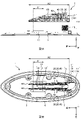
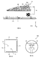
- FIG. 1 is a side view of the vehicle 100.
- FIG. 2 is a diagram illustrating an outline of the antenna device 1 of the first embodiment.
- the directions of the antenna device 1 and the like are defined.
- the front-rear direction, left-right direction, and up-down direction of the antenna device 1 are the same as the front-back direction, left-right direction, and up-down direction in the vehicle 100 in which the antenna device 1 is installed. That is, the front side (front side) from the driver's seat of the vehicle 100 is the front direction (front) of the antenna device 1, the right side from the driver's seat of the vehicle 100 is the right direction of the antenna device 1, and the zenith direction is from the driver's seat of the vehicle 100.
- the direction is upward (upward) of the antenna device 1.
- the opposite directions of the front direction, the right direction, and the upward direction are defined as the rear direction (rear direction), the left direction, and the downward direction (downward).
- the front-back direction may be referred to as a longitudinal direction
- the left-right direction may be referred to as a lateral direction or a width direction
- the vertical direction may be referred to as a vertical direction or a height direction.
- each direction of the front-back direction, the left-right direction, and the up-down direction is represented by a line segment with an arrow.
- the intersection of these line segments with arrows does not mean the origin of coordinates.
- the appearance of the antenna device 1 of the present embodiment is, for example, as shown in FIG. 4 to be described later, the front is tapered and the left and right widths are gradually narrowed upward from the mounting surface to the vehicle 100. Since it is designed as such, the features of such a design help to understand the direction and so on.
- the outer shape of the antenna device 1 (that is, the outer shape of the case 2 described later) is a fin shape (that is, a shark fin shape) that rectifies the running wind of the vehicle 100 and reduces the fluid resistance.
- the outer shape of the antenna device 1 of the present embodiment is tapered in the front and widens in the left-right direction toward the rear in the top view. Further, the outer shape of the antenna device 1 of the present embodiment gradually narrows to the left and right from the mounting surface to the vehicle 100 in the rear view. That is, the antenna device 1 of the present embodiment has a streamlined outer shape in which the width becomes relatively narrower and the height becomes lower toward the front tip, and the side surface is also a curved surface narrowed inward.
- the outer shape of the antenna device 1 is not limited to this, and may be various shapes such as a cube, a rectangular parallelepiped, a cone, a pyramid, and a sphere, and these shapes may be combined.
- the antenna device 1 of the present embodiment is installed on the rear upper surface of the roof 101 of the vehicle 100, for example, as shown in FIG.
- the installation position of the antenna device 1 can be appropriately changed according to the environmental conditions such as the assumed communication target.
- the antenna device 1 can be installed at various positions such as the upper part of the dashboard of the vehicle 100, the bumper, the license plate mounting portion, and the pillar portion.
- the antenna device 1 may be housed in a cavity between the roof panel of the vehicle 100 and the roof lining of the ceiling surface in the vehicle interior, for example.
- the roof panel of the vehicle 100 is made of, for example, an insulating resin so that the antenna device 1 can receive electromagnetic waves (hereinafter, may be referred to as "radio waves").
- the antenna device 1 housed in the cavity between the roof panel of the vehicle 100 and the roof lining of the ceiling surface in the vehicle interior is fixed to the roof lining made of an insulating resin by, for example, a screw or the like. ..
- the antenna device 1 housed in the cavity may be fixed to the frame or roof panel of the vehicle 100.
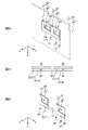
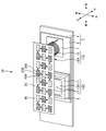
- FIG. 2 simply illustrates the antenna device 1 of the present embodiment by schematically representing the antenna device 1 and the configuration (for example, the antenna 11 described later) of the antenna device 1. Further, in FIG. 2, in order to illustrate the inside of the antenna device 1 of the present embodiment, the illustration of the case 2 described later is omitted, and the outer shape of the case 2 is shown by a broken line.
- the antenna device 1 is an antenna device having a plurality of antennas. As shown in FIG. 2, the antenna device 1 has a case 2, a base 3, a substrate 6, a substrate 7, an antenna 10, and an antenna 11.
- the case 2 is a member that forms an accommodation space for the antenna 10 and the antenna 11 together with the base 3.
- the case 2 constitutes the upper surface of the antenna device 1.
- the case 2 is made of an insulating resin material.
- the case 2 may be formed of a material other than the insulating resin material and which transmits radio waves.
- the case 2 may be composed of a portion of an insulating resin material and a portion of another material that transmits radio waves, and these materials may be freely combined.
- the case 2 is fixed to the base 3 by a screw (not shown).
- the case 2 is not limited to the case where it is fixed by screws, and may be fixed to the base 3 by snap-fitting, welding, adhesion, or the like.
- the base 3 together with the case 2 is a member that forms an accommodation space for the antenna 10 and the antenna 11.
- the base 3 constitutes the bottom surface of the antenna device 1.
- the base 3 has an insulating base 4 and a metal base 5, as shown in FIG.
- the insulating base 4 is a plate-shaped member formed of an insulating resin material.
- the insulating base 4 may be formed of a material other than the resin material as long as it is insulating, and may have a shape other than a plate shape.
- a metal base 5 is attached to the insulating base 4 with screws (not shown).
- the metal base 5 is a member that functions as a ground for the antenna device 1.
- the metal base 5 is, for example, a metal plate-shaped member, and is a die-cast product such as an aluminum alloy.
- the metal base 5 may have a shape other than a plate shape as long as it is a metal member that functions as a ground, and may be made of sheet metal.
- the metal base 5 is provided with a substrate 6 to which the antenna 10 is connected and a substrate 7 to which the antenna 11 is connected. In other words, on the metal base 5, the antenna 10 is installed via the substrate 6, and the antenna 11 is installed via the substrate 7.
- the metal base 5 functions as a ground for the antenna 10 and the antenna 11 included in the antenna device 1.
- the metal base 5 is provided as an integrated metal base on which the substrate 6 and the substrate 7 are installed, but the metal base on which the substrate 6 is installed and the metal base on which the substrate 7 is installed are separate bodies. It may be provided as a metal base of. Even when it is provided as such a separate metal base, it functions appropriately as a ground for the antenna 10 and the antenna 11.
- the antenna device 1 has the base 3 as a member constituting the bottom surface of the antenna device 1. Further, it has been described that the base 3 has an insulating base 4 and a metal base 5 that functions as a ground.
- the configuration of the base 3 is not limited to the above-mentioned case.
- the base 3 may have only the metal base 5, or may have an insulating base 4, a metal base 5, and another metal base, with a metal plate instead of the metal base. May be there. Further, the base 3 may be composed of an insulating base 4 and a metal plate instead of the metal base.
- the above-mentioned members can be freely combined as a member constituting the bottom surface of the antenna device 1 and a member functioning as a ground.
- the case 2 and the base 3 accommodate the antenna 10 and the antenna 11.
- the case 2 and the base 3 form an accommodation space for accommodating at least the antenna 10 and the antenna 11.
- the case 2 and the base 3 may accommodate members other than the antenna 10 and the antenna 11.
- the case 2 and the base 3 form a housing of the shark fin antenna.
- the board 6 is a circuit board to which the antenna 10 is connected.
- the substrate 7 is a circuit board to which the antenna 11 is connected.
- the substrate 6 and the substrate 7 are installed on the metal base 5. That is, the substrate 6 and the substrate 7 are installed on the metal base 5 as separate substrates. In this case, the cost can be suppressed by using a small substrate.
- the substrate to which the antenna 10 is connected and the substrate to which the antenna 11 is connected may be integrally formed. In this case, the assembly work of the antenna device 1 can be made more efficient.
- the antenna 10 is, for example, a planar antenna (patch antenna) corresponding to radio waves in the 1.5 GHz band (for example, L1 band) for a global positioning satellite system (GNSS: Global Navigation Satellite System). Therefore, in the following, the antenna 10 may be referred to as a "GNSS antenna” or a "patch antenna".
- the antenna 10 receives radio waves in the 1.5 GHz band for GNSS.
- the antenna 10 receives radio waves in the 1559 MHz to 1610 MHz band for the L1 band.
- the target frequency in the L1 band is the center frequency in the present embodiment, and the center frequency here is 1575.42 MHz.
- the antenna 10 may correspond to radio waves in a plurality of frequency bands, and at least one of transmission and reception of radio waves in a desired frequency band. Just do.
- the communication standard and frequency band supported by the antenna 10 are not limited to those described above, and may be other communication standards and frequency bands.
- the antenna 10 may be, for example, a flat antenna (patch antenna) corresponding to a radio wave in the 2.3 GHz band for a satellite digital radio broadcasting service (SDARS: Satellite Digital Audio Radio Service).
- SDARS Satellite Digital Audio Radio Service
- the antenna 10 is not limited to a planar antenna, and is, for example, a monopole antenna, a dipole antenna, a collinear antenna, a bow tie antenna corresponding to radio waves in the 614 MHz to 5100 MHz (5.1 GHz) band for GSM, UMTS, LTE, and 5G. , A wideband antenna based on these antennas may be used.
- the antenna 10 may be an antenna corresponding to radio waves in the frequency band used for telematics, V2X (Vehicle to Everything: vehicle-to-vehicle communication, road-to-vehicle communication), Wi-Fi, Bluetooth, and DAB. Further, the antenna 10 may be a keyless entry antenna or a smart entry antenna.
- the antenna 10 may be an antenna corresponding to communication by MIMO (Multiple-Input Multiple-Output).
- MIMO Multiple-Input Multiple-Output
- the antenna device 1 corresponds to the communication by MIMO.
- data is transmitted from each of the plurality of antennas constituting the antenna device 1, and the data is simultaneously received by the plurality of antennas.
- the antenna 10 has a dielectric member 12 and a radiating element 13.
- the dielectric member 12 is a substantially quadrilateral plate-shaped member made of a dielectric material such as ceramic. As shown in FIG. 2, a radiation element 13 is provided on the front surface of the dielectric member 12, and the back surface of the dielectric member 12 functions as a ground conductor film (or a ground conductor plate). A pattern (not shown) that is a conductor is provided.
- the dielectric member 12 may be a dielectric substrate, or may be a solid or hollow resin member.
- the "quadrilateral” means a shape consisting of four sides including, for example, a square, a rectangle, a trapezoid, a parallelogram, and the like. Further, in the shape of "substantially quadrilateral", for example, at least a part of the corners may be cut out diagonally with respect to the side. Further, in the “substantially quadrilateral” shape, a notch (concave portion) or a protrusion (convex portion) may be provided in a part of the side.
- the shape of the dielectric member 12 is not limited to a substantially quadrilateral, and may be, for example, a circle, an ellipse, or a polygon. Further, the dielectric member 12 may have a shape other than a plate shape, and may be, for example, a columnar shape, a box shape, or a tubular shape.
- the radiating element 13 is a conductive substantially quadrilateral member smaller than the area of the front surface of the dielectric member 12. As shown in FIG. 2, the radiating element 13 is provided on the front surface of the dielectric member 12.
- the shape of the radiating element 13 is not limited to a substantially quadrilateral, and may be, for example, a circle, an ellipse, or a polygon. That is, the radiating element 13 may have a shape capable of receiving and transmitting radio waves in a desired frequency band (here, 1.5 GHz band for GNSS).
- the radiating element 13 has a feeding unit 14.
- the feeding unit 14 is a portion including a feeding point in which a feeding line (not shown) is electrically connected to the radiating element 13.
- the antenna 10 of the present embodiment adopts a configuration in which two feeding lines connected to the radiating element 13 are provided, that is, a two feeding method.
- the two-feed type radiating element 13 has, for example, a substantially square shape having the same length and width so that a desired circularly polarized wave can be received.
- the "substantially square” is a shape included in the above-mentioned "substantially quadrilateral".
- the antenna 10 may adopt a configuration in which only one feeding line is connected to the radiating element 13, that is, one feeding method.
- the radiating element 13 of the one feeding system has, for example, a substantially rectangular shape having different vertical and horizontal lengths so that a desired circularly polarized wave can be received.
- the "substantially rectangular” is a shape included in the above-mentioned "substantially quadrilateral”.
- the radiating element 13 of the two feeding system or the one feeding system may be configured to be able to receive and transmit at least one of desired circular polarizations.
- the antenna 10 may adopt other power feeding methods such as a 4-feeding method in addition to the 1 feeding method and the 2 feeding method. Further, the antenna 10 may be configured to be able to receive and transmit at least one of a desired horizontal polarization and a desired linear polarization which is a desired vertical polarization.
- the antenna 10 may support radio waves in a plurality of frequency bands. Although details will be described as the second embodiment shown in FIG. 19 described later, four slots may be provided along the outer edge of the radiating element 13 of the antenna 10.
- the slot is an opening (or hole) formed in the antenna 10 to radiate (or reflect) radio waves in a desired frequency band received by the antenna 10.
- the frequency band received by the antenna 10 having the radiating element 13 with a slot is two frequency bands, a frequency band determined by the external dimensions of the radiating element 13 and a frequency band determined by the length of the slot formed in the radiating element 13. Will have. This makes it possible to configure the antenna 10 corresponding to radio waves in a plurality of frequency bands.
- the antenna 10 may be a multi-layer or multi-stage antenna.
- the antenna 10 can receive radio waves in a plurality of frequency bands.
- the element of the lower layer or the lower antenna 10 may correspond to the radio wave of the desired frequency band
- the element of the upper layer or the upper antenna 10 may correspond to the radio wave of the frequency band higher or lower than the desired frequency band.
- the antenna 11 is, for example, an antenna corresponding to a radio wave for AM / FM radio.
- the antenna 11 receives, for example, a radio wave for AM broadcasting of 522 kHz to 1710 kHz and a radio wave for FM broadcasting of 76 MHz to 108 MHz. Therefore, in the following, the antenna 11 may be referred to as an "AM / FM antenna".
- the antenna 11 may receive only one of the radio wave for AM broadcasting and the radio wave for FM broadcasting.
- the communication standard and frequency band supported by the antenna 11 are not limited to those described above, and may be other communication standards, for example, other frequency bands such as the frequency band used for DAB. It may be. Further, the antenna 11 may transmit or receive radio waves in a desired frequency band at least one of them.
- the antenna 11 has an element 15 and an element 16.
- the element 15 is an element that resonates with the element 16 in the frequency band of the radio wave for AM / FM radio. Further, the element 15 is an inductive element in the antenna 11 and may be referred to as a helical element (or simply "coil").
- the element 15 is provided on the metal base 5 via the substrate 7, as shown in FIG. Then, one end of the element 15 is connected to the substrate 7, and the other end of the element 15 is electrically connected to the element 16.
- the element 16 is an element that resonates with the element 15 in the frequency band of the radio wave for AM / FM radio.
- the element 16 is a capacitive element in the antenna 11 and may be referred to as a capacitive loading element. Other descriptions of the element 16 will be described later.
- the antenna 11 may have a holder for holding the element 15 and the element 16 in addition to the element 15 and the element 16.
- the antenna device 1 is an antenna device having a plurality of antennas, and as shown in FIG. 2, it has been described that the antenna device 1 has two antennas, an antenna 10 and an antenna 11. However, as described in the fifth embodiment shown in FIG. 28, which will be described later, the antenna device 1 may have three antennas including the antenna 19 in addition to the antenna 10 and the antenna 11. It may have four or more antennas.
- the antenna device 1 may have a pad sandwiched and fixed between the case 2 and the base 3 in addition to the above-described configuration.
- the pad has a soft insulating property, and may be configured to close the gap between the roof 101 and the case 2 to improve the aesthetic appearance and to improve dust resistance and waterproofness.
- the antenna 11 of the antenna device 1 has an element 16 that resonates in the frequency band of the radio wave for AM / FM radio together with the element 15.
- the outline of the element 16 of the antenna 11 will be described with reference to FIG. 2.
- the element 16 has a plurality of parallel resonance portions 20, an external connection portion 50, and a base material 60.
- the parallel resonance unit 20 is a member that resonates in parallel in the frequency band of the corresponding radio wave of the antenna 10 (here, the 1.5 GHz band for GNSS). Then, as shown in FIG. 2, the element 16 has a plurality of (here, 24) parallel resonance portions 20.
- the parallel resonance portions adjacent to the parallel resonance portion 20 via the external connection portion 50 are referred to as a parallel resonance portion 30 and a parallel resonance portion 40, respectively.
- the distinction between the parallel resonance portion 30 and the parallel resonance portion 40 with respect to the parallel resonance portion 20 is convenient in the sense that "they are located adjacent to the parallel resonance portion 20 via the external connection portion 50".
- the configurations of the parallel resonance portion 30 and the parallel resonance portion 40 are the same as those of the parallel resonance portion 20.
- the configurations of the parallel resonance section 30 and the parallel resonance section 40 may be partially different from those of the parallel resonance section 20.
- the parallel resonance portion 30 (or the parallel resonance portion 40) may have a different shape from the parallel resonance portion 20.
- the description of the parallel resonance section "20" is a description common to a plurality of parallel resonance sections including the parallel resonance section 20, the parallel resonance section 30, and the parallel resonance section 40, or the description of the plurality of parallel resonance sections.
- the description may be representative of any of the parallel resonance portions.
- all of the plurality of parallel resonance portions are simply referred to as the parallel resonance portion "20", or the parallel resonance portion "20" is represented by any one of the plurality of parallel resonance portions. May be called.
- the external connection portion 50 is a member that connects adjacent parallel resonance portions 20 to each other.
- connecting is not limited to physically connecting, but includes “electrically connecting”.
- electrically connecting the adjacent parallel resonance portions 20 includes, for example, connecting the adjacent parallel resonance portions 20 with a conductor, or connecting them with an electronic circuit, an electronic component, or the like.
- 23 external connection portions 50 are provided so that all 24 parallel resonance portions 20 are connected.
- the plurality of parallel resonance units 20 connected by the external connection unit 50 operate as a single conductor together with the element 15 with respect to the frequency band of the radio wave for AM / FM radio. That is, the element 16 resonates with the element 15 in the frequency band of the radio wave for AM / FM radio.
- the element 16 of the present embodiment includes a plurality of (here, 24) parallel resonance portions 20 connected by the external connection portion 50.
- the connection path of the plurality of parallel resonance portions 20 connected by the external connection portion 50 may meander.
- a parallel resonance portion may be connected so as to form a meandering path (vertical meander-shaped path) while repeating folding in the vertical direction.
- the plurality of parallel resonance portions 20 connected by the external connection portion 50 are elements with respect to the frequency band of the radio wave corresponding to the antenna 11 (here, the frequency band of the radio wave for AM / FM radio). Operates as a single conductor with 15.
- each of the plurality of parallel resonance portions 20 resonates in the frequency band of the corresponding radio wave of the antenna 10 (here, the 1.5 GHz band for GNSS), so that the antenna 11 of the present embodiment is a different antenna.
- the influence on the characteristics of (antenna 10) can be suppressed. Suppressing the influence on the characteristics of the antenna 10 will be described later together with the simulation results.
- the base material 60 is a plate-shaped member provided with a parallel resonance portion 20 and an external connection portion 50.
- the base material 60 is, for example, a printed circuit board (PCB: Printed-Circuit Board).
- the base material 60 has a conductor pattern formed on a resin material such as a glass epoxy resin.
- the base material 60 may have a conductor pattern formed on a resin material other than the glass epoxy resin such as phenol resin.
- the base material 60 may have a portion formed other than the plate shape.
- the base material 60 may be a part of the case 2 or a part of a holder (not shown) for holding the element 15 and the element 16 described above.
- the case 2 and the holder (not shown) may be made of, for example, resin.
- the base material 60 is not limited to the above-mentioned configuration, and may be composed of only a conductor pattern. Further, when the base material 60 is formed by forming a conductor pattern on the resin material, for example, MID (Molded Interconnect Device) technique may be used. This makes it possible to form a conductor pattern on a resin material having a complicated three-dimensional shape. For example, a conductor pattern can be formed by using the MID technique on a resin material having a shape like the base material 60 shown in FIG.
- MID Manufacturing Interconnect Device
- the element 16 resonates with the element 15 in the frequency band of the corresponding radio wave (here, the radio wave for AM / FM radio) of the antenna 11.
- the element 16 has a parallel resonance portion 20 that resonates in parallel in the frequency band of the corresponding radio wave (here, the radio wave for GNSS) of the antenna 10.
- the outline of the parallel resonance portion 20 constituting the element 16 will be described with reference to FIG.
- FIG. 3 is a diagram illustrating an outline of the parallel resonance portion 20, and FIG. 3A is an explanatory diagram of the parallel resonance portion 20.
- FIG. 3B is a diagram showing the parallel resonance portion 20 as a circuit diagram. Note that FIG. 3A simply illustrates the parallel resonance portion 20 by schematically representing the configuration of the parallel resonance portion 20 and the parallel resonance portion 20 (for example, the capacitor 21 and the inductor 22 described later). ..
- the parallel resonance portion 20 is not always arranged along the direction of the antenna device 1 (front-back direction, left-right direction, up-down direction), FIG. As shown in, the direction and the like (X direction, Y direction and Z direction) of the parallel resonance portion 20 are defined.
- the direction in which the capacitor 21 (described later) and the inductor 22 (described later) are lined up is the X direction. Further, the side from the inductor 22 toward the capacitor 21 is in the + X direction, and the opposite side (the side from the capacitor 21 toward the inductor 22) is in the ⁇ X direction.
- the direction in which the pair of conductors of the capacitor 21 (conductor 23 and conductor 24 described later) are lined up is the Z direction.
- the side from the conductor 24 (conductor located on the back surface 62 of the base material 60; described later) to the conductor 23 (conductor located on the front surface 61 of the base material 60; described later) is defined as the + Z direction.
- the opposite side (the side from the conductor 23 toward the conductor 24) is the ⁇ Z direction.
- the direction perpendicular to the X direction and the Z direction is defined as the Y direction. Further, the direction indicated by the arrow in FIG. 3A is defined as the + Y direction. The direction opposite to the direction indicated by the arrow is the -Y direction.
- the parallel resonance portion 20 has a capacitor 21 and an inductor 22 as shown in FIG. 3A. That is, in the parallel resonant unit 20 of the present embodiment, as shown in FIG. 3B, by configuring the parallel resonant circuit with C and L, the frequency band of the corresponding radio wave of the antenna 10 (here, 1 for GNSS). Resonates in the 5.5 GHz band).
- the capacitor 21 of the parallel resonance portion 20 corresponds to C shown in FIG. 3B
- the inductor 22 of the parallel resonance portion 20 corresponds to L shown in FIG. 3B.
- the size and shape of the capacitor 21 and the inductor 22 can be freely adjusted according to the frequency band of the corresponding radio wave of the antenna 10.
- the capacitor 21 is a region of the parallel resonant portion 20 surrounded by the alternate long and short dash line in FIG. 3A, and is a member of the parallel resonant circuit that functions as a capacitor, as represented by C in FIG. 3B.
- the capacitor 21 has a pair of conductors composed of a conductor 23 and a conductor 24, which are located so as to face each other.
- the inductor 22 is a region of the parallel resonant portion 20 other than the region surrounded by the alternate long and short dash line in FIG. 3A, and is a member of the parallel resonant circuit that functions as a coil as represented by L in FIG. 3B. ..
- the inductor 22 is connected to the capacitor 21 in parallel.
- the inductor 22 has an arm portion 27, an arm portion 28, and an internal connection portion 29.
- the arm portion 27 extends from the conductor 23, and the arm portion 28 extends from the conductor 24.
- the internal connection portion 29 is a member that connects the arm portion 27 and the arm portion 28.
- the conductor 23 and the arm portion 27 are located on the front surface 61 of the base material 60.
- the conductor 24 and the arm 28 are located on the back surface 62 of the base material 60.
- the "front surface” of the base material 60 is the surface of the plate surface of the element 16 of the parallel resonance portion 20 on the side facing the case 2.
- the "back surface” of the base material 60 is a surface opposite to the side facing the case 2.
- the front surface 61 and the back surface 62 are surfaces facing each other.
- the internal connection portion 29 connects the arm portion 27 located on the front surface 61 of the base material 60 and the arm portion 28 located on the back surface 62 of the base material 60. ..
- the shape, dimensions, etc. of the capacitor 21 and the inductor 22 can be freely adjusted according to the desired frequency band of the resonating radio wave.
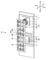
- FIG. 4 is a perspective view of the antenna device 1 of the first embodiment.
- 5A and 5B are views of the antenna device 1 of the first embodiment,
- FIG. 5A is a side view of the antenna device 1
- FIG. 5B is a plan view of the antenna device 1.
- 6A and 6B are views of the parallel resonance section 20
- FIG. 6A is a perspective view of the parallel resonance section 20
- FIG. 6B is an exploded perspective view of the parallel resonance section 20.
- FIG. 7 is a six-view view of the parallel resonance portion 20.
- the plan view shown in FIG. 5B is a view of the antenna device 1 from above. Further, in FIG. 7, when the parallel resonance portion 20 is viewed in the ⁇ Z direction, (a) left side view, (b) top view, (c) front view, (d) bottom view, (e). ) The right side view and (f) the rear view are shown.
- the first region A1 is a region in which the antenna 10 exists in the side view or the top view, and as shown in FIGS. 5A and 5B, the first region A1 is the rearmost region from the frontmost end portion of the antenna 10. The area to the end.
- the second region A2 is a region where the antenna 11 exists in the side view or the top view, and as shown in FIGS. 5A and 5B, the rearmost end from the frontmost end portion of the antenna 11 It is the area up to the part.
- the first region A1 of the antenna 10 is included in the second region A2 of the antenna 11.
- the second region A2 of the antenna 11 may be included in the first region A1 of the antenna 10 because the antenna 10 is formed larger than the antenna 11.
- the antenna 10 is arranged so as to be displaced to the front side with respect to the antenna 11, a part of the first region A1 of the antenna 10 may be included in the second region A2 of the antenna 11.
- a part of the first region A1 of the antenna 10 is included in the second region A2 of the antenna 11
- a part of the first region A1 of the antenna 10 and a part of the second region A2 of the antenna 11 are included. It will be duplicated.
- the first region A1 of the antenna 10 and the second region A2 of the antenna 11 may not overlap.
- the first region A1 of the antenna 10 is included in the second region A2 of the antenna 11.
- the second region A2 of the antenna 11 may be included in the first region A1 of the antenna 10 because the antenna 10 is formed larger than the antenna 11.
- the antenna 10 is arranged so as to be offset to the right or left side with respect to the antenna 11, a part of the first region A1 of the antenna 10 may be included in the second region A2 of the antenna 11.
- a part of the first region A1 of the antenna 10 is included in the second region A2 of the antenna 11
- a part of the first region A1 of the antenna 10 and a part of the second region A2 of the antenna 11 are included. It will be duplicated.
- the first region A1 of the antenna 10 and the second region A2 of the antenna 11 may not overlap.
- the antenna device 1 of the present embodiment at least a part of the first region A1 of the antenna 10 and at least a part of the second region A2 of the antenna 11 overlap in the side view and the top view.
- the first region A1 of the antenna 10 and the second region A2 of the antenna 11 overlap, while in the top view, the first region A1 of the antenna 10 and the second region A2 of the antenna 11 are overlapped. And may be non-overlapping.
- the plurality of parallel resonant units 20 operate as a single conductor together with the element 15 with respect to the frequency band of the radio wave for AM / FM radio. Further, the plurality of parallel resonance portions 20 resonate in the frequency band of the corresponding radio wave of the antenna 10 (here, the 1.5 GHz band for GNSS). Then, the plurality of parallel resonance portions 20 can suppress the influence when operating as a single conductor with respect to the frequency band of the corresponding radio wave of the antenna 10. As a result, even when the position or region of the antenna 10 and the position or region of the antenna 11 overlap each other, the influence of the antenna 11 (particularly, the element 16) on the characteristics of the antenna 10 can be suppressed.
- the element 16 is composed of two aggregates, an aggregate 17 and an aggregate 18, as shown in the top view of FIG. 5B.
- Each of the aggregate 17 and the aggregate 18 has a plurality of parallel resonance portions 20, an external connection portion 50, and a base material 60. Then, the aggregate 17 and the aggregate 18 are separated from each other and are connected to the element 15, respectively.
- Each of the aggregate 17 and the aggregate 18 is inclined with respect to the plane perpendicular to the plate surface of the base 3. Specifically, the aggregate 17 is inclined toward the left side toward the lower side, while the aggregate 18 is inclined toward the right side toward the lower side. That is, the distance from one point on the lower edge of the aggregate 17 to one point on the lower edge of the opposing aggregate 18 is from one point on the upper edge of the aggregate 17 to one point on the upper edge of the opposing aggregate 18. It is larger than the distance of. That is, the aggregate 17 and the aggregate 18 of the present embodiment are configured such that the distance between the upper edge portions is smaller than the distance between the lower edge portions.
- the outer shape of the antenna device is a fin shape (that is, a shark fin shape)
- the element 16 can be arranged along the inner shape of the fin-shaped case 2, so that the space inside the case 2 can be arranged. It is possible to secure the characteristics of the antenna 11 while making the best use of.
- the aggregate 17 and the aggregate 18 may be arranged parallel to the plane perpendicular to the plate surface of the base 3 or may be arranged parallel to the plate surface of the base 3.
- the element 16 is not limited to two aggregates, and may be composed of three or more aggregates. Further, the element 16 may be composed of only one aggregate, or may be configured as a single plate-shaped member as shown in the explanatory view of the antenna device 1 shown in FIG.
- the configuration may be such that the aggregate 17 and the upper edge portions of the aggregate 18 are connected to each other (the aggregate 17 and the upper edges of the aggregate 18 are connected to each other). Inverted V-shaped or inverted U-shaped shown in FIGS. 11B and 11C). Further, the aggregate 17 and the lower edge portions of the aggregate 18 may be connected to each other (V-shaped or U-shaped). Further, in the aggregate 17 and the aggregate 18 of the present embodiment, the distance between the upper edges is smaller than the distance between the lower edges, but the distance between the upper edges is smaller than the distance between the lower edges. It may be configured to be larger than the distance between the parts.
- the aggregate when the element 16 is composed of one aggregate, the aggregate may be arranged parallel to the plane perpendicular to the plate surface of the base 3 (I-shaped shape). Further, when the element 16 is composed of one aggregate, the aggregate may be arranged in parallel with the plate surface of the base 3 (the shape of the minus sign).
- the parallel resonance unit 20 has a capacitor 21 and an inductor 22.
- the capacitor 21 is a region of the parallel resonant portion 20 surrounded by the alternate long and short dash line in FIG. 6A
- the inductor 22 is a region of the parallel resonant portion 20 other than the region surrounded by the alternate long and short dash line of FIG. 6A. ..
- the parallel resonance portion 20 has a configuration in which a pair of plate-shaped members constituting the capacitor 21 and the inductor 22 are connected by the internal connection portion 29. .. Specifically, the portion composed of the conductor 23 and the arm portion 27 located on the front surface 61 of the base material 60, and the conductor 24 and the arm portion 28 located on the back surface 62 of the base material 60. The portion composed of and is connected by the internal connection portion 29. With such a configuration, the parallel resonance portion 20 is formed as a distributed constant circuit.
- the maximum dimension of the parallel resonance portion 20 is configured to be small.
- the maximum dimension is the distance between the two longest points among the distances between the two points in the outer shape of the parallel resonance portion 20.
- the maximum dimension is, for example, a diagonal line in a three-dimensional shape, and a portion of the maximum dimension of each side (length, width, height, thickness, diameter) forming a structure.
- the maximum dimension of the parallel resonance portion 20 is 1/10 or less of the wavelength of the corresponding radio wave of the antenna 10.
- the maximum dimension of the parallel resonance portion 20 may be larger than 1/10 of the wavelength of the corresponding radio wave of the antenna 10 as long as the influence on the characteristics of the antenna 10 can be suppressed.
- the internal connection portion 29 is located closer to the center of the outer shape than the outer edge of the outer shape of the parallel resonance portion 20.
- the "center” is the geometric center in the outer shape of the parallel resonance portion 20. That is, the arm portion 27 of the inductor 22 is formed so as to extend inward from the outer peripheral side of the outer shape of the parallel resonance portion 20 after extending from the conductor 23 of the capacitor 21.
- the arm 27 of the inductor 22 extends from the conductor 23 of the capacitor 21 and forms a spiral that swirls from the outer edge side of the outer shape of the parallel resonant portion 20 toward the center, or the arm of the inductor 22.
- the portion 27 forms a spiral that swirls from the center of the outer shape of the parallel resonance portion 20 toward the outer edge, and is connected to the conductor 23 of the capacitor 21.
- the arm portion 28 of the inductor 22 is formed so as to extend inward from the outer peripheral side of the outer shape of the parallel resonance portion 20 after extending from the conductor 24 of the capacitor 21.
- the arm 28 of the inductor 22 extends from the conductor 24 of the capacitor 21 and forms a spiral that swirls from the outer edge side of the outer shape of the parallel resonant portion 20 toward the center, or the arm of the inductor 22.
- the portion 28 forms a spiral that swirls from the center of the outer shape of the parallel resonance portion 20 toward the outer edge, and is connected to the conductor 24 of the capacitor 21.
- the arm portion 27 and the arm portion 28 are connected by an internal connection portion 29 on the side of the center of the outer shape of the parallel resonance portion 20 with respect to the outer edge of the outer shape.
- the position of the internal connection portion 29 is limited to the center side of the outer shape of the parallel resonance portion 20. However, it may be on the outer edge side of the outer shape of the resonance parallel portion 20.
- the internal connection portion 29 is a conductor portion formed by a through hole or a via hole formed in the base material 60. As a result, the arm portion 27 and the arm portion 28 are connected.
- the outer shape of the parallel resonance portion 20 is a quadrilateral, more specifically. , Approximately square.
- the outer shape of the parallel resonance portion 20 may be a quadrilateral or a circle other than a substantially square, as in the modified example of the parallel resonance portion 20 shown in FIGS. 13 to 18 described later.
- the outer shape of the parallel resonance portion 20 is not shown, it may have any shape such as a polygon such as a triangle or a pentagon, an ellipse, a semicircle, or a semi-elliptical shape, and the above-mentioned shape may be used. It may be configured in combination.
- the parallel resonance portion 20 of the present embodiment has a connection region 25 connected to the adjacent parallel resonance portion 30 and a connection region 26 connected to the adjacent parallel resonance portion 40.
- the connection area 26 is located on the back surface 62 other than the area facing the connection area 25.
- the connection area 25 is located on the front surface 61 other than the area facing the connection area 26.
- connection region 26 has a straight line passing through the center of the outer shape of the parallel resonance portion 20 as an axis with respect to the region facing the connection region 25 on the back surface 62. It is located in a region that is line-symmetrical or point-symmetrical at the center of the outer shape of the parallel resonance portion 20.
- connection region 25 is line-symmetrical with respect to the region facing the connection region 26 on the front surface 61, or line symmetry about the straight line passing through the center of the outer shape of the parallel resonance portion 20, or the parallel resonance portion 20. It is located in a region that is point-symmetrical at the center of the outer shape.
- FIG. 8 is a view of adjacent parallel resonance portions 20 and 30,
- FIG. 8A is a perspective view of adjacent parallel resonance portions 20 and 30, and
- FIG. 8B is a side view of adjacent parallel resonance portions 20 and 30.
- 8C is an exploded perspective view in which adjacent parallel resonance portions 20 and 30 are separated from each other.
- the parallel resonance unit 30 also has a capacitor 31 and an inductor 32, similarly to the parallel resonance unit 20.
- the capacitor 31 has a pair of conductors, which are composed of a conductor 33 located on the front surface 61 and a conductor 34 located on the back surface 62, which are located so as to face each other.
- the inductor 32 is connected in parallel to the capacitor 31 and has an arm portion 37, an arm portion 38, and an internal connection portion 39 connecting the arm portion 37 and the arm portion 38.
- the external connection portion 50 connects the capacitor 21 of the parallel resonance portion 20 and the capacitor 31 of the parallel resonance portion 30.
- the external connection portion 50 is located on the back surface of the conductor 23 located on the front surface of the capacitor 21 of the parallel resonance portion 20 and the capacitor 31 of the parallel resonance portion 30. It is connected to the conductor 34.
- the external connection portion 50 is a conductor portion formed by a through hole or a via hole formed in the base material 60. As a result, the conductor 23 and the conductor 34 are connected.
- the maximum dimension of the external connection portion 50 is also small as in the parallel resonance portion 20. By making the maximum dimension of the external connection portion 50 small, it is possible to suppress the influence on the characteristics of the antenna 10.
- the maximum dimension of the external connection portion 50 is 1/10 or less of the wavelength of the radio wave corresponding to the antenna 10.
- the maximum dimension of the external connection portion 50 may be larger than 1/10 of the wavelength of the corresponding radio wave of the antenna 10 as long as the influence on the characteristics of the antenna 10 can be suppressed.
- FIG. 9 is a view of the antenna device 1X of the comparative example
- FIG. 9A is a side view of the antenna device 1X
- FIG. 9B is a plan view of the antenna device 1X.
- the element 16 of the antenna 11 of the present embodiment described above has the aggregates 17 and 18 including a plurality of parallel resonance portions 20.
- the element 16X of the antenna 11X of the comparative example is composed of one metal body.
- the element 16X of the comparative example has a shape in which the left and right metal body portions are connected by the upper (top) metal body portion, and has a shape as if one metal plate is bent. Has. Therefore, in the element 16X of the comparative example, the element 16 is not configured by the plurality of parallel resonance portions 20 and the external connection portion 50 as in the antenna 11 of the present embodiment.
- the configuration of the antenna device 1X of the comparative example other than the configuration of the element 16X is the same as that of the antenna device 1 of the present embodiment. That is, the antenna 11X is configured so that the element 16X and the element 15 resonate in the frequency band of the radio wave for AM / FM radio. Further, the antenna 10 and the antenna 11X are located so that at least a part of the first region A1 of the antenna 10 and at least a part of the second region A2 of the antenna 11X overlap.
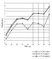
- FIG. 10 is a diagram showing the relationship between the elevation angle and the average gain of the antenna 10 in each of the antenna device 1 of the first embodiment and the antenna device 1X of the comparative example.
- the horizontal axis represents the elevation angle and the vertical axis represents the average gain.
- the calculation result of the antenna 10 in the antenna device 1X of the comparative example is shown by a alternate long and short dash line and a cross
- the calculation result of the antenna 10 in the antenna device 1 of the present embodiment is shown by a solid line and a + mark.
- the calculation results in the configuration of only the antenna 10 are shown by broken lines and circles.
- the average gain is significantly improved at each elevation angle. ing. Further, when the calculation result of the antenna 10 in the antenna device 1 of the present embodiment and the calculation result in the configuration of only the antenna 10 are compared, the decrease in the average gain at each elevation angle is considerably small. From this, the antenna 11 in the antenna device 1 of the present embodiment can suppress the influence on the characteristics of the antenna 10.
- FIG. 11 is a diagram showing a modification of the cross-sectional shape of the element 16
- FIG. 11A is an explanatory view showing a first modification of the cross-sectional shape of the element 16
- FIG. 11B is a diagram showing a first modification of the cross-sectional shape of the element 16.
- 2 is an explanatory diagram showing a modified example
- FIG. 11C is an explanatory diagram showing a third modified example of the cross-sectional shape of the element 16.
- 11A to 11C are cross-sectional views when the element 16 is cut along a plane perpendicular to the front-rear direction.
- the cross-sectional shape of the element 16 of the first modification is an I-shape as shown in FIG. 11A. That is, the element 16 has a flat plate shape perpendicular to the left-right direction. However, the flat plate-shaped element 16 may have a shape inclined by a predetermined angle with respect to at least one of the vertical direction and the horizontal direction.
- the element 16 may have a flat plate shape perpendicular to the vertical direction.
- the cross-sectional shape of the element 16 is the shape of the minus sign. Even if the cross-sectional shape of the element 16 is formed in this way, the element 16 can appropriately resonate with the element 15 in the frequency band of the radio wave for AM / FM radio.
- the element 16 of the first modification can also suppress the influence on the characteristics of the antenna 10.
- the cross-sectional shape of the element 16 of the second modification is an inverted U-shape that is convex upward.
- the element 16 may have a U-shape that is convex downward. Even if the cross-sectional shape of the element 16 is formed in this way, the element 16 can appropriately resonate with the element 15 in the frequency band of the radio wave for AM / FM radio.
- the element 16 of the second modification can also suppress the influence on the characteristics of the antenna 10.
- the cross-sectional shape of the element 16 of the third modification is an inverted V-shape that is convex upward.
- the element 16 may have a V-shape that is convex downward. Even if the cross-sectional shape of the element 16 is formed in this way, the element 16 can appropriately resonate with the element 15 in the frequency band of the radio wave for AM / FM radio.
- the element 16 of the third modification can also suppress the influence on the characteristics of the antenna 10.
- the cross-sectional shape of the element 16 is a shape along a side other than the bottom of the trapezoidal side.
- connection path of the parallel resonance portion in the element 16 is changed by changing the connection between the adjacent parallel resonance portions (that is, changing the position of the external connection portion 50). You can change the connection route of.
- the element 16 is an element that resonates with the element 15 in the frequency band of the radio wave for AM / FM radio, and functions as a capacitive loading element in the antenna 11.
- any parallel resonance portion connection path may be used. That is, the external connection portion 50 may be positioned in any way with respect to the plurality of parallel resonance portions 20. Therefore, the modification shown below is a specific example of the connection path of the parallel resonance portion, and the connection path of the parallel resonance portion other than the modification shown below may be configured.
- FIG. 12 is a diagram showing a modification of the connection path of the parallel resonance portion in the element 16
- FIG. 12A is a first modification of the connection path of the parallel resonance portion in the element 16
- FIG. 12B is a modification of the element 16.
- FIG. 12C is a second modification of the connection path of the parallel resonance portion
- FIG. 12C is a third modification of the connection path of the parallel resonance portion in the element 16.
- connection path of the parallel resonance portion in the element 16 in the first modification is a path that meanders while repeatedly folding back and forth (horizontal meander-shaped path). Even if the connection path of the parallel resonance portion in the element 16 is configured in this way, the element 16 can appropriately resonate with the element 15 in the frequency band of the radio wave for AM / FM radio. In addition, the influence on the characteristics of the antenna 10 can be suppressed. Furthermore, the degree of freedom in design can be improved.
- connection path of the parallel resonance portion in the element 16 in the second modification is a path that meanders while irregularly folding back and forth in the front-rear direction and the left-right direction. Even if the connection path of the parallel resonance portion in the element 16 is configured in this way, the element 16 can appropriately resonate with the element 15 in the frequency band of the radio wave for AM / FM radio. In addition, the influence on the characteristics of the antenna 10 can be suppressed. Furthermore, the degree of freedom in design can be improved.
- connection path of the parallel resonance portion in the element 16 is configured so as to pass through all the parallel resonance portions 20 shown in the figure with a single stroke.
- the parallel resonance portion 20 located in the left two rows meanders while repeating folding in the left-right direction, while the parallel resonance portion 20 located in the right one row meanders. It is connected by branching from each of the routes. Even if the connection path of the parallel resonance portion in the element 16 is configured in this way, the element 16 can appropriately resonate with the element 15 in the frequency band of the radio wave for AM / FM radio. In addition, the influence on the characteristics of the antenna 10 can be suppressed. Furthermore, the degree of freedom in design can be improved.
- connection route does not have to be a meandering route.
- connection path may be configured to go around, swirl, or linearly.
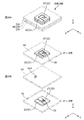
- FIG. 13 is a perspective view of a first modification of the parallel resonance portion 20.
- FIG. 14 is a six-view view of the first modification of the parallel resonance portion 20.
- FIG. 14 when the parallel resonance portion 20 of the first modification is viewed in the ⁇ Z direction as a front view, (a) left side view, (b) top view, (c) front view, and (d) bottom view. , (E) right side view, (f) rear view.
- the outer shape of the parallel resonance portion 20 shown in FIGS. 6 and 7 described above was substantially square in a plan view.
- the outer shape of the parallel resonance portion 20 of the first modification is substantially rectangular in a plan view. More specifically, it is a substantially rectangular shape having a length in the Y direction longer than that in the X direction.
- the outer shape of the parallel resonance portion 20 of the first modification may be a substantially rectangular shape having a length in the X direction longer than that in the Y direction.
- the shape of the element 16 composed of the plurality of parallel resonance portions 20 can be flexibly formed. For example, even in the region at the end of the element 16 where the substantially square parallel resonance portion 20 cannot be arranged, the substantially rectangular parallel resonance portion 20 can be arranged. Thereby, for example, the parallel resonance portion 20 can be arranged without waste in the element 16 as in the parallel resonance portion 20 located at the upper part of the element 16 in FIG. 5, and the capacitance of the element 16 can be increased.
- the element 16 may be formed by arranging a substantially rectangular parallel resonance portion 20, or may be formed by arranging the element 16 in combination with a substantially square parallel resonance portion 20.
- FIG. 15 is a perspective view of a second modification of the parallel resonance portion 20.
- FIG. 16 is a six-view view of the second modification of the parallel resonance portion 20.
- the left side view, (b) top view, (c) front view, and (d) bottom view are viewed from the front when the parallel resonance portion 20 of the second modification is viewed in the ⁇ Z direction.
- connection region 25 and the connection region 26 in the parallel resonance portion 20 shown in FIGS. 6 and 7 described above were arranged side by side in the Y-axis direction as shown in FIG. 6B.
- the connection region 25 and the connection region 26 in the parallel resonance portion 20 of the second modification are located diagonally. That is, when viewed in a three-dimensional structure, the connection area 25 and the connection area 26 are located farthest from each other.
- the element 16 may be formed by arranging only the parallel resonance portion 20 of the second modification, or the parallel resonance portion 20 shown in FIGS. 6 and 7 and the parallel resonance portion 20 of the second modification. May be combined and arranged, or may be arranged and formed in combination with the parallel resonance portion 20 of the first modification.
- FIG. 17 is a perspective view of a third modification of the parallel resonance portion 20.
- FIG. 18 is a six-view view of a third modification of the parallel resonance portion 20.
- the outer shape of the parallel resonance portion 20 of the third modification is substantially circular in a plan view.
- the outer shape of the parallel resonance portion 20 of the third modification may be elliptical or semi-circular.
- the connection region 25 and the connection region 26 in the parallel resonance portion 20 of the third modification are arranged side by side in the Y-axis direction.
- the element 16 may be formed by arranging only the parallel resonance portion 20 of the third modification, or the parallel resonance portion 20 shown in FIGS. 6 and 7 and the parallel resonance portion 20 of the third modification. May be arranged and formed in combination, or may be arranged and formed in combination with the parallel resonance portion 20 of the second modification.
- the antenna device 1 of the first embodiment has been described. That is, the antenna 10 of the antenna device 1 of the first embodiment corresponds to radio waves in one frequency band (for example, 1.5 GHz band for GNSS). However, the antenna included in the antenna device may correspond to radio waves in a plurality of frequency bands. Therefore, in the following, the antenna device 1 of the second embodiment having the antenna 10A corresponding to the radio waves of a plurality of frequency bands will be described.
- FIG. 19A is a view of the antenna device 1A of the second embodiment
- FIG. 19A is a side view of the antenna device 1A
- FIG. 19B is a plan view of the radiating element 13A of the antenna 10A
- FIG. 19C is an enlarged view of the external connection portion 50A.
- the radiating element 13A of the antenna 10A is provided with four slots 70 along the outer edge of the radiating element 13A.
- the slot 70 is an opening (or hole) formed in the antenna 10A to radiate (or reflect) radio waves in a desired frequency band received by the antenna 10A.
- the frequency band received by the antenna 10A having the radiating element 13A with the slot 70 is two, a frequency band determined by the external dimensions of the radiating element 13A and a frequency band determined by the length of the slot 70 formed in the radiating element 13A. Will have a frequency band.
- the shape of the slot 70 shown in FIG. 19B is substantially rectangular, but is not limited to this shape, and may be curved so as to be convex toward the center of the radiating element, or at least one convex portion. It may be a shape having or a corrugated shape. Further, the slots 70 shown in FIG. 19B are provided at four places, but the present invention is not limited to this, and a plurality of slots corresponding to radio waves of different frequency bands may be provided, and three different antennas 10A may be provided. It may be configured to correspond to radio waves in the above frequency bands.
- the antenna 10A can receive, for example, radio waves in two frequency bands of the above-mentioned L1 band and L2 band.
- the antenna 10A receives, for example, radio waves in the 1212 MHz to 1254 MHz band for the L2 band in addition to the L1 band.
- the target frequency in the L2 band is the center frequency in this embodiment, and the center frequency here is 1227.6 MHz.
- the antenna 10A having the radiating element 13A is not limited to the L1 band and the L2 band, and may receive radio waves in two desired frequency bands, or may receive radio waves in three or more frequency bands. Further, the antenna 10A having the radiating element 13A may transmit and receive radio waves in a plurality of desired frequency bands at least one of them.
- a notch may be formed in the radiating element 13A instead of the slot 70.
- the slot 70 may have a meander portion. As a result, the total length of the slot 70 becomes longer and the electric length also increases as compared with the slot 70 having no meander portion shown in FIG. 19B. Then, in the case of the slot 70 having the meander portion, the resonance frequency determined by the radiating element 13A can be lowered, and the degree of freedom in setting the two frequency bands of the radio wave received by the antenna 10A can be improved.
- the antenna 10A may be a multi-layer or multi-stage antenna in order to receive radio waves in a plurality of frequency bands.
- the element of the lower layer or the lower antenna 10A may correspond to the radio wave of the desired frequency band
- the element of the upper layer or the upper antenna 10A may correspond to the radio wave of the frequency band higher or lower than the desired frequency band.
- the element 16A of the antenna 11A has an external connection portion 50A different from that of the first embodiment, as shown in FIGS. 19A and 19C.
- the other configurations of the antenna device 1A are the same as those of the antenna device 1 of the first embodiment.
- the external connection unit 50A is composed of a lumped constant circuit. As shown in FIG. 19C, the external connection portion 50A configured by the lumped constant circuit is a parallel resonant circuit composed of a capacitor portion C and an inductor portion L. However, the external connection portion 50A configured by the lumped constant circuit may be configured only by the inductor portion L, or may be a combination of elements capable of forming a parallel resonance circuit.
- one terminal of the external connection portion 50A is connected to the parallel resonance portion 20, and the other terminal is connected to the parallel resonance portion 30 adjacent to the parallel resonance portion 20.
- the external connection portion 50A configured by the lumped constant circuit is provided so as to straddle the adjacent parallel resonance portion 20 and the parallel resonance portion 30.
- the parallel resonance portion 20 of the element 16A resonates in one frequency band (for example, the L1 band) among the plurality of frequency bands of the corresponding radio waves of the antenna 10A.
- the external connection portion 50A of the element 16A resonates in another frequency band (for example, L2 band) among the plurality of frequency bands of the corresponding radio waves of the antenna 10A. ..
- FIG. 20 is a diagram illustrating an outline of the antenna device 1B of the third embodiment.
- 21 is a view of the parallel resonance portion 20B
- FIG. 21A is a perspective view of the parallel resonance portion 20B
- FIG. 21B is an exploded perspective view of the parallel resonance portion 20B.
- FIG. 22 is a hexagonal view of the parallel resonance portion 20B.
- FIG. 20 simply illustrates the antenna device 1B by schematically showing the configuration (for example, the antenna 11B described later) of the antenna device 1B and the antenna device 1B.
- the detailed shape and configuration of the antenna device 1B of the present embodiment are the same as those of the antenna device 1 of the first embodiment shown in FIGS. 4 and 5 except for the case described below. Further, in FIG. 20, in order to illustrate the inside of the antenna device 1B, the illustration of the case 2 is omitted.
- the antenna device 1B of the present embodiment has an antenna 10B corresponding to radio waves in a plurality of frequency bands such as the L1 band and the L2 band.
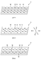
- the element 16B of the antenna 11B resonates with, for example, a parallel resonance portion (for example, a parallel resonance portion 20B) that resonates in the frequency band of the L1 band and, for example, in the frequency band of the L2 band. It has a parallel resonance portion (for example, a parallel resonance portion 30B and a parallel resonance portion 40B). That is, the element 16B has two types of parallel resonance portions having different resonance frequencies from each other. As a result, it is possible to suppress the influence on the characteristics of the antenna 10B corresponding to the radio waves of a plurality of frequency bands (here, the L1 band and the L2 band).
- the parallel resonance portion (parallel resonance portion 20B in FIG. 20) that resonates in one frequency band among the two types of parallel resonance portions having different resonance frequencies is referred to as “parallel resonance portion in the A frequency band”. May be called.
- the parallel resonance portion of the A frequency band is illustrated by hatching with dots.
- the parallel resonance portion (parallel resonance portion 30B and parallel resonance portion 40B in FIG. 20) that resonates in another frequency band is referred to as "parallel resonance in the B frequency band.
- Part the parallel resonance portion of the B frequency band is illustrated by hatching with diagonal lines.
- FIGS. 21 and 22 illustrate the detailed configuration of the parallel resonance portion 20B, which is the parallel resonance portion of the A frequency band.
- the configuration of the parallel resonance portion 20B, which is the parallel resonance portion of the A frequency band, is as shown in FIG. 6 and FIG. It is the same as the configuration of the parallel resonance unit 20 of the first embodiment shown in FIG. 7.
- the parallel resonance portion of the A frequency band and the parallel resonance portion of the B frequency band are alternately arranged one by one as shown in FIG. Further, in the element 16B of the present embodiment, the parallel resonance portion of the A frequency band and the parallel resonance portion of the B frequency band are arranged on the base material 60 having a one-layer structure.
- the present invention is not limited to this, for example, the parallel resonance portion 20B corresponding to the radio wave in the A frequency band, the parallel resonance portion 30B corresponding to the radio wave in the B frequency band, and the C frequency band different from the A frequency band and the B frequency band.
- the parallel resonance portion 40B corresponding to the radio wave of the above may be arranged to correspond to the radio wave of three frequency bands. Further, the mode of arrangement of the parallel resonance portion 20B is not limited to these cases. Therefore, in the following, a modification relating to the arrangement of the parallel resonance portion 20B will be described.
- FIG. 23 is an explanatory diagram of a first modification regarding the arrangement of the parallel resonance portion 20B.
- an arbitrary number of parallel resonance portions in the A frequency band and parallel resonance portions in the B frequency band may be alternately arranged.
- the parallel resonance portion of the A frequency band and the parallel resonance portion of the B frequency band may be irregularly arranged.
- FIG. 24 is a diagram showing a second modification regarding the arrangement of the parallel resonance portions 20B
- FIG. 24A is a perspective view of adjacent parallel resonance portions 20B and 30B
- FIG. 24B is a perspective view of adjacent parallel resonance portions 20B. It is an exploded perspective view which separated 30B.
- FIG. 25 is a six-view view of adjacent parallel resonance portions 20B and 30B.
- the base material 60 is formed of a multilayer structure. Specifically, the base material 60 is composed of three dielectric layers, that is, a dielectric layer 63, a dielectric layer 64, and a dielectric layer 65.
- the dielectric layer 63 is a layer of the base material 60 located on the front surface side.
- the dielectric layer 65 is a layer of the base material 60 located on the back surface side.
- the dielectric layer 64 is a layer of the base material 60 located between the dielectric layer 63 and the dielectric layer 65.
- the dielectric layer 63 is provided with a parallel resonance portion 30B.
- the dielectric layer 65 is provided with a parallel resonance portion 20B.
- the dielectric layer 64 is provided with an external connection portion 50B for connecting the parallel resonance portion 20B and the parallel resonance portion 30B.
- the parallel resonance portion 20B and the parallel resonance portion 30B are positioned so as to overlap each other in the thickness direction of the base material (Z direction in FIG. 24). That is, in the second modification, the parallel resonance portion 20B and the parallel resonance portion 30B are laminated.
- the entire parallel resonance portion 20B and the entire parallel resonance portion 30B substantially overlap, but for example, they may be positioned so as to be shifted from each other in at least one direction of the X direction and the Y direction. However, a part of the parallel resonance portion 20B and a part of the parallel resonance portion 30B may be positioned so as to overlap each other.
- the adjacent parallel resonance portion 20B and the parallel resonance portion 30B are provided on the base material 60 formed of a single-layer structure.
- adjacent parallel resonance portions 20B and parallel resonance portions 30B can be arranged on the base material 60 formed of the multilayer structure. .. Even with such an arrangement, it is possible to suppress the influence on the characteristics of the antenna 10B corresponding to the radio waves of a plurality of frequency bands (here, the L1 band and the L2 band).
- connection path of the parallel resonance portion in the element 16 of the first embodiment has been described.
- connection path of the parallel resonance portion in the element 16B is changed by changing the connection with the adjacent parallel resonance portions (that is, changing the position of the external connection portion 50B). be able to.
- FIG. 26 is a diagram showing a modification of the connection path of the parallel resonance portion in the element 16B
- FIG. 26A is an explanatory diagram of a first modification of the connection path of the parallel resonance portion in the element 16B
- FIG. 26B is an explanatory diagram
- FIG. 26C is an explanatory diagram of a second modification of the connection path of the parallel resonance portion in the element 16B
- FIG. 26C is an explanatory diagram of a third modification of the connection path of the parallel resonance portion in the element 16B.
- connection path of the parallel resonance portion in the element 16B in the first modification is a path that meanders while repeatedly folding back and forth (horizontal meander-shaped path).
- the connection path of the parallel resonance portion in the element 16B may be a path that meanders while being folded back in the vertical direction (a path having a vertical meander shape). Even if the connection path of the parallel resonance portion in the element 16B is configured in this way, the element 16B can appropriately resonate with the element 15 in the frequency band of the radio wave for AM / FM radio. In addition, the degree of freedom in design can be improved.
- connection path of the parallel resonance portion in the element 16B in the second modification is a path that meanders while irregularly folding back and forth in the front-rear direction and the left-right direction. Even if the connection path of the parallel resonance portion in the element 16B is configured in this way, the element 16B can appropriately resonate with the element 15 in the frequency band of the radio wave for AM / FM radio. In addition, the degree of freedom in design can be improved.
- connection path of the parallel resonance portion in the element 16B is configured so as to pass through all the parallel resonance portions 20B shown in the figure with a single stroke.
- the parallel resonance portion 20B located in the left two rows meanders while repeating folding in the left-right direction, while the parallel resonance portion 20B located in the right one row meanders. It is connected by branching from each of the routes. Even if the connection path of the parallel resonance portion in the element 16B is configured in this way, the element 16B can appropriately resonate with the element 15 in the frequency band of the radio wave for AM / FM radio. In addition, the degree of freedom in design can be improved.
- connection route does not have to be a meandering route.
- connection path may be configured to swirl and orbit, or may be configured to be linear.
- the antenna device 1B of the third embodiment has been described. That is, the antenna 10B of the antenna device 1B of the third embodiment corresponds to radio waves of two frequency bands (for example, L1 band and L2 band). However, the antenna included in the antenna device may correspond to radio waves in three frequency bands. Therefore, in the following, the antenna device 1 of the fourth embodiment having the antenna 10C corresponding to the radio waves of the three frequency bands will be described.
- FIG. 27 is a view of the antenna device 1C of the fourth embodiment
- FIG. 27A is a side view of the antenna device 1C
- FIG. 27B is an enlarged view of the external connection portion 50C.
- the antenna 10B of the third embodiment can receive radio waves in two frequency bands, for example, the L1 band and the L2 band.
- the antenna 10C of the present embodiment can receive radio waves in the frequency band of, for example, the L5 band in addition to the L1 band and the L2 band.
- the antenna 10C receives radio waves in the 1164 MHz to 1214 MHz band for the L5 band in addition to the L1 band and the L2 band.
- the target frequency in the L5 band is the center frequency in this embodiment, and the center frequency here is 1176.45 MHz. That is, the antenna 10C of the present embodiment can receive radio waves in three frequency bands.
- the element 16C has an external connection portion 50C similar to that of the second embodiment described above. That is, the external connection portion 50C is configured by a lumped constant circuit. As shown in FIG. 27C, the external connection portion 50C configured by the lumped constant circuit is a parallel resonant circuit composed of a capacitor portion C and an inductor portion L. However, the external connection portion 50C configured by the lumped constant circuit may be configured only by the inductor portion L, or may be a combination of elements capable of forming a parallel resonance circuit.
- one terminal of the external connection portion 50C is connected to the parallel resonance portion 20C, and the other terminal is connected to the parallel resonance portion 30C adjacent to the parallel resonance portion 20C.
- an external connection portion 50C configured by a lumped constant circuit is provided so as to straddle the adjacent parallel resonance portions 20C and parallel resonance portions 30C.
- the element 16C has, for example, a parallel resonance portion (for example, a parallel resonance portion 20C) that resonates in the frequency band of the L1 band.
- a parallel resonance portion for example, a parallel resonance portion 30C and a parallel resonance portion 40C that resonate in the frequency band of the L2 band.
- the external connection portion 50C resonates in another radio wave frequency band (for example, L5 band) among the plurality of radio wave frequency bands corresponding to the antenna 10C.
- another radio wave frequency band for example, L5 band
- the antenna device 1C is the same as those of the antenna device 1B of the third embodiment.
- one patch antenna for example, antenna 10
- the AM / FM antenna for example, antenna 11
- a plurality of antennas may be located in the vicinity of the AM / FM antenna (for example, the antenna 11). That is, another antenna may be provided as in the antenna device 1D of the present embodiment.
- FIG. 28 is a perspective view of the antenna device 1D of the fifth embodiment.
- the antenna device 1D has an antenna 10, an antenna 11, and an antenna 19.
- the antenna 10 and the antenna 11 in the antenna device 1D of the present embodiment are, for example, the same antennas as the antenna 10 and the antenna 11 in the antenna device 1 of the first embodiment. That is, the antenna 10 is a patch antenna corresponding to a radio wave in the 1.5 GHz band for GNSS, and the antenna 11 is an antenna corresponding to a radio wave for AM / FM radio.
- the antenna 19 further possessed by the antenna device 1D of the present embodiment is, for example, a patch antenna corresponding to a radio wave in the 2.3 GHz band for SDARS. That is, in the antenna device 1D, the frequency band of the corresponding radio wave of the antenna 10 and the frequency band of the corresponding radio wave of the antenna 19 are different.
- the antenna 19 is not limited to the patch antenna, and may be in another antenna type such as a monopole antenna, a dipole antenna, a collinear antenna, or a bow tie antenna, and may be a telematics antenna, a V2X antenna, a Wi-Fi antenna, or the like. It may be an antenna corresponding to various frequency bands such as a blue-tooth antenna, a keyless antenna, and a smart key antenna.
- the element 16D is, for example, the same as the element 16A in the second embodiment shown in FIG. That is, the plurality of parallel resonance portions 20D of the element 16D resonate in the frequency band of the corresponding radio wave of the antenna 10 (for example, the 1.5 GHz band for GNSS). Further, the external connection portion 50D of the element 16D is configured by a lumped constant circuit and resonates in the frequency band of the corresponding radio wave of the antenna 19 (for example, the 2.3 GHz band for SDARS). This makes it possible to suppress the influence on the characteristics of the plurality of antennas (antenna 10 and antenna 19).
- the element 16D may be the same as the element 16B of the third embodiment shown in FIG. 20, for example. That is, the element 16D has a parallel resonance portion (for example, parallel resonance portion 20D) that resonates in the frequency band of the corresponding radio wave of the antenna 10 and a parallel resonance portion (for example, parallel) that resonates in the frequency band of the corresponding radio wave of the antenna 19. It may have a resonance portion 30D and a parallel resonance portion 40D). This makes it possible to suppress the influence on the characteristics of the plurality of antennas (antenna 10 and antenna 19).
- the antenna 11 includes a plurality of parallel resonance portions 20, 30, and 40 that resonate in the 1.5 GHz band (L1 band) for GNSS.
- the element 16 having an external connection portion 50 for connecting adjacent parallel resonance portions (parallel resonance portions 20, 30 or parallel resonance portions 20, 40), and the element 16 It comprises an element 15 to be connected.
- the element 16 and the element 15 are different from the 1.5 GHz band (L1 band) for GNSS, for example, the frequency band for AM / FM radio (522 kHz to 1710 kHz for AM broadcasting and 76 MHz to 108 MHz). Corresponds to radio waves (for FM broadcasting). According to such an antenna 11, it is possible to suppress the influence on the characteristics of another antenna (antenna 10).
- the 1.5 GHz band (L1 band) for GNSS corresponds to the "first frequency band”
- the frequency band for AM / FM radio corresponds to the "second frequency band”.
- the external connection portion 50 corresponds to the "first connection portion”.
- the element 16 corresponds to the "first element”
- the element 15 corresponds to the "second element”.
- the element 16 has a base material 60, and a plurality of parallel resonance portions 20, 30, and 40 are provided on the base material 60. ing. Thereby, the element 16 of the antenna 11 that suppresses the influence on the characteristics of another antenna (antenna 10) can be easily configured.
- the maximum dimension of the parallel resonance portion 20 is, for example, one tenth or less of the wavelength of the 1.5 GHz band (L1 band) for GNSS. This makes it possible to suppress the influence on the characteristics of another antenna (antenna 10).
- the length of the external connection portion 50 is, for example, one tenth or less of the wavelength of the 1.5 GHz band (L1 band) for GNSS. This makes it possible to suppress the influence on the characteristics of another antenna (antenna 10).
- the outer shape of the parallel resonance portion 20 is a quadrilateral, a polygon, or a circle.
- the parallel resonance portion 20 has a capacitor 21 having a pair of conductors 23 and 24 located so as to face each other, and a capacitor 21. It has an inductor 22 connected in parallel to the capacitor 22.
- the parallel resonance unit 20 can be resonated in, for example, the 1.5 GHz band (L1 band) for GNSS.
- the inductor 22 has an inside connecting one conductor 23 and the other conductor 24 of the pair of conductors 23 and 24.
- the connecting portion 29 is provided, and in the plan view of the parallel resonance portion 20, the internal connecting portion 29 is located closer to the center of the outer shape than the outer edge of the outer shape of the parallel resonance portion 20. As a result, the maximum dimension of the parallel resonance portion 20 can be reduced.
- the element 16 has a base material 60
- the parallel resonance portion 20 is a conductor 23 and a conductor operating as a capacitor 21.
- an arm portion 27 extending from the conductor 23 and an arm portion 28 extending from the conductor 24, and an internal connecting portion 29 connecting the arm portion 27 and the arm portion 28 while operating as an inductor 22.
- the conductor 23 and the arm portion 27 are located on the front surface 61 of the base material 60
- the conductor 24 and the arm portion 28 are located on the back surface 62 facing the front surface 61 of the base material 60. do.
- the element 16 of the antenna 11 that suppresses the influence on the characteristics of another antenna (antenna 10) can be easily configured.
- the conductor 23 corresponds to the "first conductor”
- the conductor 24 corresponds to the "second conductor”.
- the arm portion 27 corresponds to the "first arm portion”
- the arm portion 28 corresponds to the "second arm portion”.
- the front surface 61 corresponds to the "first surface”
- the back surface 62 corresponds to the "second surface”.
- the arm portion 28 is located closer to the center of the outer shape than the outer edge of the outer shape of the parallel resonance portion 20. As a result, the maximum dimension of the parallel resonance portion 20 can be reduced.
- the plurality of parallel resonance portions include a parallel resonance portion 30, a parallel resonance portion 20, and a parallel resonance portion 40.
- the parallel resonance portion 30 and the parallel resonance portion 20 are adjacent to each other, and the parallel resonance portion 20 and the parallel resonance portion 40 are arranged so as to be adjacent to each other.
- the parallel resonance portion 20 has a connection region 25 for connecting the parallel resonance portion 30 and the parallel resonance portion 20, and a connection region 26 for connecting the parallel resonance portion 20 and the parallel resonance portion 40.
- the connection region 25 is located on the front surface 61 of the base material 60
- the connection region 26 is located on the back surface 62 of the base material 60.
- the element 16 of the antenna 11 that suppresses the influence on the characteristics of another antenna can be easily configured. Further, since the positions of the adjacent parallel resonance portions 30 (or the adjacent parallel resonance portions 40) can be flexibly set with respect to the parallel resonance portion 20, the degree of freedom in design can be improved.
- the parallel resonance portion 30 corresponds to the "first parallel resonance portion”
- the parallel resonance portion 20 corresponds to the “second parallel resonance portion”
- the parallel resonance portion 40 corresponds to the "third parallel resonance portion”.
- the connection area 25 corresponds to the "first connection area”
- the connection area 26 corresponds to the "second connection area”.
- connection area 26 is located on the back surface 62 other than the area facing the connection area 25.
- the element 16 of the antenna 11 that suppresses the influence on the characteristics of another antenna (antenna 10) can be easily configured.
- the positions of the adjacent parallel resonance portions 30 (or the adjacent parallel resonance portions 40) can be flexibly set with respect to the parallel resonance portion 20, the degree of freedom in design can be improved.
- connection region 26 is the parallel resonance portion 20 with respect to the region facing the connection region 25 on the back surface 62. It is located in a region that is line-symmetrical about a straight line passing through the center of the outer shape or point-symmetrical at the center of the outer shape of the parallel resonance portion 20.
- the element 16 of the antenna 11 that suppresses the influence on the characteristics of another antenna (antenna 10) can be easily configured.
- the positions of the adjacent parallel resonance portions 30 (or the adjacent parallel resonance portions 40) can be flexibly set with respect to the parallel resonance portion 20, the degree of freedom in design can be improved.
- the antenna 11 for example, as shown in FIG. 6B, at least one of the parallel resonance portion 30 and the parallel resonance portion 40 is connected to at least one of the connection region 25 and the connection region 26.
- the element 16 of the antenna 11 that suppresses the influence on the characteristics of another antenna (antenna 10) can be easily configured.
- the positions of the adjacent parallel resonance portions 30 (or the adjacent parallel resonance portions 40) can be flexibly set with respect to the parallel resonance portion 20, the degree of freedom in design can be improved.
- At least one of the parallel resonance portion 30 and the parallel resonance portion 40 corresponds to “another parallel resonance portion”.
- the parallel resonance portion is a distributed constant circuit.
- the element 16 of the antenna 11 that suppresses the influence on the characteristics of another antenna (antenna 10) can be easily configured.
- connection paths of the plurality of parallel resonance portions 20, 30 and 40 connected by the external connection portion 50 are meandering.
- the element 16 of the antenna 11 that suppresses the influence on the characteristics of another antenna (antenna 10) can be easily configured.
- the degree of freedom in design can be improved.
- the external connection portion 50A is a lumped constant circuit, and the lumped constant circuit is for 1.5 GHz band (L1 band) for GNSS and for AM / FM radio. Resonates in, for example, the L2 band, which is different from the frequency band of. This makes it possible to suppress the influence on the characteristics of another antenna (antenna 10A) corresponding to radio waves in a plurality of frequency bands.
- the L2 band corresponds to the "third frequency band”.
Abstract
Description
まず、本実施形態のアンテナ装置1について説明する前に、図1及び図2を参照しつつ、アンテナ装置1の方向等の定義、及びアンテナ装置1の外形及び設置位置を説明する。 == 1st embodiment ==
First, before explaining the
以下では、図1及び図2に示されるように、アンテナ装置1の方向等(前後方向、左右方向及び上下方向)を定義する。アンテナ装置1の前後方向、左右方向及び上下方向は、アンテナ装置1を設置した車両100における前後方向、左右方向及び上下方向と同一とする。つまり、車両100の運転席からフロント側(前側)をアンテナ装置1の前方向(前方)とし、車両100の運転席から右側をアンテナ装置1の右方向とし、車両100の運転席から天頂方向をアンテナ装置1の上方向(上方)とする。また、前方向、右方向及び上方向の各々の反対方向を、後方向(後方)、左方向及び下方向(下方)とする。なお、前後方向を長手方向、左右方向を横方向又は幅方向、上下方向を縦方向又は高さ方向と呼ぶことがある。 << Definition of direction, etc. >>
In the following, as shown in FIGS. 1 and 2, the directions of the
次に、図2を参照しつつ、本実施形態におけるアンテナ装置1の概要を説明する。なお、図2では、アンテナ装置1、及びアンテナ装置1が有する構成(例えば、後述するアンテナ11など)を模式的に表すことで、本実施形態のアンテナ装置1を簡易に図示している。また、図2では、本実施形態のアンテナ装置1の内部を図示するために、後述するケース2の図示を省略し、ケース2の外形を破線で示している。 << Overview of
Next, the outline of the
ケース2は、ベース3とともに、アンテナ10及びアンテナ11の収容空間を形成する部材である。本実施形態では、ケース2は、アンテナ装置1の上面を構成する。また、本実施形態では、ケース2は、絶縁性の樹脂材料により形成されている。但し、ケース2は、絶縁性の樹脂材料以外で、かつ電波を透過する材料により形成されても良い。また、ケース2は、絶縁性の樹脂材料の部分と、電波を透過する他の材料の部分とで構成されても良く、これらの材料を自由に組み合わせても良い。なお、ケース2は、不図示のネジによりベース3に固定されている。但し、ケース2は、ネジにより固定される場合に限られず、スナップフィット、溶着、接着などでベース3に固定されても良い。 <
The
ベース3は、ケース2とともに、アンテナ10及びアンテナ11の収容空間を形成する部材である。本実施形態では、ベース3は、アンテナ装置1の底面を構成する。ベース3は、図2に示されるように、絶縁ベース4と、金属ベース5とを有する。 <
The
基板6は、アンテナ10が接続される回路基板である。また、基板7は、アンテナ11が接続される回路基板である。基板6と、基板7とは、前述したように、金属ベース5に設置されている。つまり、基板6と、基板7とは、別体の基板として金属ベース5に設置されている。この場合、小型の基板を用いることでコストを抑制することができる。しかし、アンテナ10が接続される基板と、アンテナ11が接続される基板とが、一体に形成されていても良い。この場合、アンテナ装置1の組立作業を効率化することができる。 <
The
アンテナ10は、例えば、全球測位衛星システム(GNSS:Global Navigation Satellite System)用の1.5GHz帯(例えば、L1バンド)の電波に対応する平面アンテナ(パッチアンテナ)である。このため、以下では、アンテナ10を、「GNSSアンテナ」又は「パッチアンテナ」と呼ぶことがある。本実施形態では、アンテナ10は、GNSS用の1.5GHz帯の電波を受信する。特に、本実施形態では、アンテナ10は、L1バンド用の1559MHz~1610MHz帯の電波を受信する。また、L1バンドにおけるターゲット周波数は、本実施形態では中心周波数であり、ここでの中心周波数は、1575.42MHzである。なお、アンテナ10は、後述する第2実施形態~第5実施形態で説明するように、複数の周波数帯の電波に対応しても良く、所望の周波数帯の電波を送信及び受信のうち少なくとも一方をすれば良い。 <
The
アンテナ11は、例えば、AM/FMラジオ用の電波に対応するアンテナである。本実施形態では、アンテナ11は、例えば、522kHz~1710kHzのAM放送用の電波と、76MHz~108MHzのFM放送用の電波とを受信する。このため、以下では、アンテナ11を、「AM/FMアンテナ」と呼ぶことがある。 <
The
アンテナ装置1は、図2では不図示であるが、上述した構成のほか、ケース2とベース3との間に挟み込まれて固定されるパッドを有しても良い。パッドは、軟質絶縁性であり、ルーフ101とケース2との隙間を塞ぎ、美観を向上させるとともに、防塵、防水性を向上させる構成としても良い。 <Other configurations>
Although not shown in FIG. 2, the
アンテナ装置1のアンテナ11は、上述したように、エレメント15とともに、AM/FMラジオ用の電波の周波数帯で共振するエレメント16を有する。以下では、引き続き図2を参照しつつ、アンテナ11のエレメント16の概要を説明する。 << Overview of
As described above, the
エレメント16は、上述したように、エレメント15とともにアンテナ11の対応する電波(ここでは、AM/FMラジオ用の電波)の周波数帯で共振する。そして、エレメント16は、アンテナ10の対応する電波(ここでは、GNSS用の電波)の周波数帯で並列共振する並列共振部20を有する。以下では、図3を参照しつつ、エレメント16を構成する並列共振部20の概要を説明する。 << Overview of Parallel
As described above, the
次に、上述において概要を説明したエレメント16及び並列共振部20について、図4~図7を参照しつつ、具体的な構成について説明する。 << Details of
Next, a specific configuration of the
まず、エレメント16の詳細について説明するために、アンテナ10とアンテナ11との位置関係について説明する。本実施形態のアンテナ装置1では、図5A及び図5Bに示されるように、アンテナ10の第1領域A1の少なくとも一部と、アンテナ11の第2領域A2の少なくとも一部とが重複するよう、アンテナ10とアンテナ11とが位置している。 <Positional relationship between
First, in order to explain the details of the
本実施形態では、エレメント16は、図5Bの上面視に示されるように、集合体17と、集合体18との2つの集合体で構成されている。集合体17と、集合体18との各々は、複数の並列共振部20と、外部接続部50と、基材60とを有する。そして、集合体17と、集合体18とは、互いに離間しており、エレメント15に各々接続される。 <Details of
In the present embodiment, the
上述したように、並列共振部20は、キャパシタ21と、インダクタ22とを有する。なお、キャパシタ21は、並列共振部20のうち、図6Aの一点鎖線で囲まれる領域であり、インダクタ22は、並列共振部20のうち、図6Aの一点鎖線で囲まれる領域以外の領域である。 <Details of
As described above, the
次に、前述で概要を説明した外部接続部50について、図8を参照しつつ、具体的な構成について説明する。 << Details of
Next, a specific configuration of the
次に、本実施形態のアンテナ11の特性について説明するために、図9に示される比較例のアンテナ11Aを説明する。 << Comparative example >>
Next, in order to explain the characteristics of the
図10は、第1実施形態のアンテナ装置1及び比較例のアンテナ装置1Xのそれぞれにおける、アンテナ10の仰角及び平均利得の関係を示す図である。 << Comparison of characteristics of
FIG. 10 is a diagram showing the relationship between the elevation angle and the average gain of the
次に、図11を参照しつつ、エレメント16の断面形状についての変形例を説明する。 << Modification example of cross-sectional shape of
Next, a modified example of the cross-sectional shape of the
第1変形例のエレメント16の断面形状は、図11Aに示されるように、I字形状である。すなわち、エレメント16は、左右方向に垂直な平板形状である。ただし、平板形状のエレメント16が、上下方向及び左右方向の少なくとも一方の方向に対して所定角度傾いた形状であっても良い。 <First modification of the cross-sectional shape of the
The cross-sectional shape of the
第2変形例のエレメント16の断面形状は、図11Bに示されるように、上側に凸となる逆U字形状である。但し、エレメント16は、下側に凸となるU字形状であっても良い。エレメント16の断面形状をこのように形成しても、エレメント16は、エレメント15とともに、適切にAM/FMラジオ用の電波の周波数帯で共振することができる。そして、第2変形例のエレメント16によっても、アンテナ10の特性に与える影響を抑制することができる。 <Second modification of the cross-sectional shape of the
As shown in FIG. 11B, the cross-sectional shape of the
第3変形例のエレメント16の断面形状は、図11Cに示されるように、上側に凸となる逆V字形状である。但し、エレメント16は、下側に凸となるV字形状であっても良い。エレメント16の断面形状をこのように形成しても、エレメント16は、エレメント15とともに、適切にAM/FMラジオ用の電波の周波数帯で共振することができる。そして、第3変形例のエレメント16によっても、アンテナ10の特性に与える影響を抑制することができる。 <Third modification example of the cross-sectional shape of the
As shown in FIG. 11C, the cross-sectional shape of the
以上のように、エレメント16の断面形状の第1変形例~第3変形例をそれぞれ説明した。なお、上述のエレメント16の断面形状の第1変形例~第3変形例を自由に組み合わせることができる。このように、エレメント16の断面形状の第1変形例~第3変形例を組み合わせた場合であっても、エレメント15とともに、適切にAM/FMラジオ用の電波の周波数帯で共振し、アンテナ10の特性に与える影響を抑制することができる。 <Combination of the first modification to the third modification of the cross-sectional shape of the
As described above, the first modification to the third modification of the cross-sectional shape of the
次に、図12を参照しつつ、エレメント16における並列共振部の接続経路についての変形例を説明する。以下で説明するエレメント16における並列共振部の接続経路の変形例では、隣り合う並列共振部同士との接続を変える(すなわち、外部接続部50の位置を変える)ことによって、エレメント16における並列共振部の接続経路を変えることができる。 << Modification example of the connection path of the parallel resonance portion in the
Next, with reference to FIG. 12, a modified example of the connection path of the parallel resonance portion in the
第1変形例におけるエレメント16における並列共振部の接続経路は、図12Aに示されるように、前後方向に折り返しを繰り返しながら蛇行する経路(横ミアンダ形状の経路)である。エレメント16における並列共振部の接続経路をこのように構成しても、エレメント16は、エレメント15とともに、適切にAM/FMラジオ用の電波の周波数帯で共振することができる。また、アンテナ10の特性に与える影響を抑制することができる。さらに、設計の自由度を向上させることができる。 <First modification of the connection path of the parallel resonance portion in the
As shown in FIG. 12A, the connection path of the parallel resonance portion in the
第2変形例におけるエレメント16における並列共振部の接続経路は、図12Bに示されるように、前後方向・左右方向に不規則に折り返しながら蛇行する経路である。エレメント16における並列共振部の接続経路をこのように構成しても、エレメント16は、エレメント15とともに、適切にAM/FMラジオ用の電波の周波数帯で共振することができる。また、アンテナ10の特性に与える影響を抑制することができる。さらに、設計の自由度を向上させることができる。 <Second modification of the connection path of the parallel resonance portion in the
As shown in FIG. 12B, the connection path of the parallel resonance portion in the
第1変形例及び第2変形例では、図に示される全ての並列共振部20を一筆書きで通過するように、エレメント16における並列共振部の接続経路が構成されていた。しかし、第3変形例では、左側の2列に位置する並列共振部20においては、左右方向に折り返しを繰り返しながら蛇行しつつ、右側の1列に位置する並列共振部20においては、これらの蛇行する経路からそれぞれ分岐して接続されている。エレメント16における並列共振部の接続経路をこのように構成しても、エレメント16は、エレメント15とともに、適切にAM/FMラジオ用の電波の周波数帯で共振することができる。また、アンテナ10の特性に与える影響を抑制することができる。さらに、設計の自由度を向上させることができる。 <Third modification example of the connection path of the parallel resonance portion in the
In the first modification and the second modification, the connection path of the parallel resonance portion in the
なお、上述では、エレメント16における並列共振部の接続経路の第1変形例~第3変形例をそれぞれ説明したが、上述の第1変形例~第3変形例を自由に組み合わせることができる。 <Combination of the first modification to the third modification of the connection path of the parallel resonance portion in the
In the above description, the first modification to the third modification of the connection path of the parallel resonance portion in the
次に、図13~図18を参照しつつ、並列共振部20の変形例を説明する。 << Modification example of
Next, a modification of the
図13は、並列共振部20の第1変形例の斜視図である。図14は、並列共振部20の第1変形例の六面図である。 <First modification of the
FIG. 13 is a perspective view of a first modification of the
図15は、並列共振部20の第2変形例の斜視図である。図16は、並列共振部20の第2変形例の六面図である。 <Second modification of the
FIG. 15 is a perspective view of a second modification of the
図17は、並列共振部20の第3変形例の斜視図である。図18は、並列共振部20の第3変形例の六面図である。 <Third modification example of the
FIG. 17 is a perspective view of a third modification of the
なお、上述では、並列共振部20の第1変形例~第3変形例をそれぞれ説明したが、上述の第1変形例~第3変形例の並列共振部20及び図6-図7に示される並列共振部20の少なくとも2つを自由に組み合わせて配置してもよい。 <Combination of the first modification to the third modification of the
In the above description, the first modification to the third modification of the
以上では、第1実施形態のアンテナ装置1について説明した。つまり、第1実施形態のアンテナ装置1のアンテナ10は、1つの周波数帯(例えば、GNSS用の1.5GHz帯)の電波に対応している。しかし、アンテナ装置が有するアンテナは、複数の周波数帯の電波に対応しても良い。そこで、以下では、複数の周波数帯の電波に対応するアンテナ10Aを有する第2実施形態のアンテナ装置1について説明する。 == Second embodiment ==
In the above, the
<<エレメント16B>>
上述した第2実施形態のアンテナ装置1Aでは、エレメント16Aが集中定数回路によって構成される外部接続部50Aを有することにより、複数の周波数帯の電波に対応するアンテナ10Aの特性に与える影響を抑制することができる。しかし、第2実施形態と異なる構成によっても、複数の周波数帯の電波に対応するアンテナの特性に与える影響を抑制することができる。そこで、以下では、複数の周波数帯の電波に対応するアンテナ10Bを有する第3実施形態のアンテナ装置1Bについて説明する。 == Third embodiment ==
<<
In the antenna device 1A of the second embodiment described above, since the
<並列共振部20Bの配置に関する第1変形例>
図23は、並列共振部20Bの配置に関する第1変形例の説明図である。 << Modification example regarding the arrangement of the
<First modification example regarding the arrangement of the
FIG. 23 is an explanatory diagram of a first modification regarding the arrangement of the
図24は、並列共振部20Bの配置に関する第2変形例を示す図であり、図24Aは、隣り合う並列共振部20B,30Bの斜視図であり、図24Bは、隣り合う並列共振部20B,30Bを離間させた分解斜視図である。図25は、隣り合う並列共振部20B,30Bの六面図である。 <Second modification example regarding the arrangement of the
FIG. 24 is a diagram showing a second modification regarding the arrangement of the
第1変形例におけるエレメント16Bにおける並列共振部の接続経路は、図26Aに示されるように、前後方向に折り返しを繰り返しながら蛇行する経路(横ミアンダ形状の経路)である。あるいは、エレメント16Bにおける並列共振部の接続経路は、上下方向に折り返しながら蛇行する経路(縦ミアンダ形状の経路)であってもよい。エレメント16Bにおける並列共振部の接続経路をこのように構成しても、エレメント16Bは、エレメント15とともに、適切にAM/FMラジオ用の電波の周波数帯で共振することができる。また、設計の自由度を向上させることができる。 <First modification of the connection path of the parallel resonance portion in the
As shown in FIG. 26A, the connection path of the parallel resonance portion in the
第2変形例におけるエレメント16Bにおける並列共振部の接続経路は、図26Bに示されるように、前後方向・左右方向に不規則に折り返しながら蛇行する経路である。エレメント16Bにおける並列共振部の接続経路をこのように構成しても、エレメント16Bは、エレメント15とともに、適切にAM/FMラジオ用の電波の周波数帯で共振することができる。また、設計の自由度を向上させることができる。 <Second modification of the connection path of the parallel resonance portion in the
As shown in FIG. 26B, the connection path of the parallel resonance portion in the
第1変形例及び第2変形例では、図に示される全ての並列共振部20Bを一筆書きで通過するように、エレメント16Bにおける並列共振部の接続経路が構成されていた。しかし、第3変形例では、左側の2列に位置する並列共振部20Bにおいては、左右方向に折り返しを繰り返しながら蛇行しつつ、右側の1列に位置する並列共振部20Bにおいては、これらの蛇行する経路からそれぞれ分岐して接続されている。エレメント16Bにおける並列共振部の接続経路をこのように構成しても、エレメント16Bは、エレメント15とともに、適切にAM/FMラジオ用の電波の周波数帯で共振することができる。また、設計の自由度を向上させることができる。 <Third modification example of the connection path of the parallel resonance portion in the
In the first modification and the second modification, the connection path of the parallel resonance portion in the
なお、上述では、エレメント16並列共振部20Bにおける並列共振部の接続経路の第1変形例~第3変形例をそれぞれ説明したが、上述の第1変形例~第3変形例を自由に組み合わせることができる。 <Combination of the first modification to the third modification of the connection path of the parallel resonance portion in the
In the above description, the first modification to the third modification of the connection path of the parallel resonance portion in the
以上では、第3実施形態のアンテナ装置1Bについて説明した。つまり、第3実施形態のアンテナ装置1Bのアンテナ10Bは、2つの周波数帯(例えば、L1バンド及びL2バンド)の電波に対応している。しかし、アンテナ装置が有するアンテナは、3つの周波数帯の電波に対応しても良い。そこで、以下では、3つの周波数帯の電波に対応するアンテナ10Cを有する第4実施形態のアンテナ装置1について説明する。 == Fourth Embodiment ==
In the above, the
上述した第1実施形態~第4実施形態のアンテナ装置(例えば、アンテナ装置1)では、AM/FMアンテナ(例えば、アンテナ11)の近傍には、1つのパッチアンテナ(例えば、アンテナ10)が位置していた。但し、AM/FMアンテナ(例えば、アンテナ11)の近傍には、複数のアンテナが位置しても良い。つまり、本実施形態のアンテナ装置1Dのように、さらに別のアンテナを有しても良い。 == Fifth Embodiment ==
In the antenna device (for example, antenna device 1) of the first to fourth embodiments described above, one patch antenna (for example, antenna 10) is located in the vicinity of the AM / FM antenna (for example, antenna 11). Was. However, a plurality of antennas may be located in the vicinity of the AM / FM antenna (for example, the antenna 11). That is, another antenna may be provided as in the
以上、本発明の実施の形態であるアンテナ11,11Aについて説明した。アンテナ11は、例えば、図2,図4,図5に示されるように、例えば、GNSS用の1.5GHz帯(L1バンド)で共振する複数の並列共振部20,30,40と、複数の並列共振部20,30,40のうち、隣り合う並列共振部同士(並列共振部20,30又は並列共振部20,40)を接続する外部接続部50と、を有するエレメント16と、エレメント16と接続されるエレメント15と、を備える。そして、エレメント16と、エレメント15とで、GNSS用の1.5GHz帯(L1バンド)とは異なる、例えば、AM/FMラジオ用の周波数帯(522kHz~1710kHzのAM放送用と、76MHz~108MHzのFM放送用)の電波に対応する。このようなアンテナ11によれば、別のアンテナ(アンテナ10)の特性に与える影響を抑制することができる。 == Summary ==
The
2 ケース
3 ベース
4 絶縁ベース
5 金属ベース
6,7,8 基板
10,10A アンテナ(GNSSアンテナ,パッチアンテナ)
11,11A,11B,11X アンテナ(AM/FMアンテナ)
12 誘電体部材
13,13A 放射素子
14 給電部
15 エレメント
16,16B,16X エレメント
17,18 集合体
19 アンテナ
20,20B 並列共振部
21 キャパシタ
22 インダクタ
23,24 導電体
25,26 接続領域
27,28 腕部
29 内部接続部
30,30B 並列共振部
31 キャパシタ
32 インダクタ
33,34 導電体
35,36 接続領域
37,38 腕部
39 内部接続部
40,40B 並列共振部
50,50A~50C 外部接続部
60 基材
61 おもて面
62 うら面
63~65 誘電層
70 スロット
100 車両
101 ルーフ
1,1A ~ 1D,
11,11A, 11B, 11X antenna (AM / FM antenna)
12
Claims (16)
- 第1周波数帯で共振する複数の並列共振部と、前記複数の並列共振部のうち、隣り合う前記並列共振部同士を接続する第1接続部と、を有する第1エレメントと、
前記第1エレメントと接続される第2エレメントと、を備え、
前記第1エレメントと、前記第2エレメントとで前記第1周波数帯とは異なる第2周波数帯の電波に対応する、
アンテナ。 A first element having a plurality of parallel resonance portions that resonate in the first frequency band and a first connection portion that connects the adjacent parallel resonance portions among the plurality of parallel resonance portions.
A second element connected to the first element is provided.
The first element and the second element correspond to radio waves in a second frequency band different from the first frequency band.
antenna. - 前記第1エレメントは、基材を有し、
前記複数の並列共振部は前記基材に設けられている、
請求項1に記載のアンテナ。 The first element has a base material and has a base material.
The plurality of parallel resonance portions are provided on the base material.
The antenna according to claim 1. - 前記並列共振部の最大寸法が、前記第1周波数帯の波長の10分の1以下である、
請求項1又は2に記載のアンテナ。 The maximum dimension of the parallel resonance portion is 1/10 or less of the wavelength of the first frequency band.
The antenna according to claim 1 or 2. - 前記第1接続部の長さが、前記第1周波数帯の波長の10分の1以下である、
請求項1から3のいずれか一項に記載のアンテナ。 The length of the first connection portion is one tenth or less of the wavelength of the first frequency band.
The antenna according to any one of claims 1 to 3. - 前記並列共振部の平面視において、前記並列共振部の外形は、四辺形、多角形、円形、楕円形、半円形、及び半楕円形のいずれかの形状又はいずれかの形状の組み合わせである、
請求項1から4のいずれか一項に記載のアンテナ。 In the plan view of the parallel resonance portion, the outer shape of the parallel resonance portion is any shape of a quadrilateral, a polygon, a circle, an ellipse, a semicircle, and a semi-elliptical shape, or a combination of any of the shapes.
The antenna according to any one of claims 1 to 4. - 前記並列共振部は、
互いに対向するように位置する一対の導電体を有するキャパシタと、
前記キャパシタに並列に接続されるインダクタと、を有する、
請求項1から5のいずれか一項に記載のアンテナ。 The parallel resonance portion is
Capacitors with a pair of conductors located facing each other,
With an inductor connected in parallel to the capacitor.
The antenna according to any one of claims 1 to 5. - 前記インダクタは、前記一対の導電体の一方の導電体と他方の導電体とを接続する第2接続部を有し、
前記並列共振部の平面視において、前記第2接続部は、前記並列共振部の外形の外縁よりも前記外形の中心の側に位置する、
請求項6に記載のアンテナ。 The inductor has a second connecting portion that connects one conductor of the pair of conductors to the other conductor.
In a plan view of the parallel resonance portion, the second connection portion is located closer to the center of the outer shape than the outer edge of the outer shape of the parallel resonance portion.
The antenna according to claim 6. - 前記第1エレメントは、基材を有し、
前記並列共振部は、
キャパシタとして動作する第1導電体及び第2導電体と、
インダクタとして動作するとともに、前記第1導電体から延在する第1腕部及び前記第2導電体から延在する第2腕部と、
前記第1腕部及び前記第2腕部を接続する第2接続部と、を有し、
前記第1導電体及び前記第1腕部は、前記基材の第1面に位置し、
前記第2導電体及び前記第2腕部は、前記基材の前記第1面に対向する第2面に位置する、
請求項1から6のいずれか一項に記載のアンテナ。 The first element has a base material and has a base material.
The parallel resonance portion is
The first conductor and the second conductor that operate as capacitors,
A first arm portion extending from the first conductor and a second arm portion extending from the second conductor while operating as an inductor.
It has a first arm portion and a second connection portion that connects the second arm portion.
The first conductor and the first arm portion are located on the first surface of the base material.
The second conductor and the second arm portion are located on the second surface of the base material facing the first surface.
The antenna according to any one of claims 1 to 6. - 前記並列共振部の平面視において、前記第2接続部は、前記並列共振部の外形の外縁よりも前記外形の中心の側に位置する、
請求項8に記載のアンテナ。 In a plan view of the parallel resonance portion, the second connection portion is located closer to the center of the outer shape than the outer edge of the outer shape of the parallel resonance portion.
The antenna according to claim 8. - 前記複数の並列共振部は、第1並列共振部と、第2並列共振部と、第3並列共振部と、を有し、
前記第1並列共振部と前記第2並列共振部とが隣り合い、前記第2並列共振部と前記第3並列共振部とが隣り合うように配置され、
前記第2並列共振部は、前記第1並列共振部と前記第2並列共振部とを接続する第1接続領域と、前記第2並列共振部と前記第3並列共振部とを接続する第2接続領域と、を有し、
前記第1接続領域は、前記基材の前記第1面に位置し、
前記第2接続領域は、前記基材の前記第2面に位置する、
請求項8又は9に記載のアンテナ。 The plurality of parallel resonance portions include a first parallel resonance portion, a second parallel resonance portion, and a third parallel resonance portion.
The first parallel resonance portion and the second parallel resonance portion are adjacent to each other, and the second parallel resonance portion and the third parallel resonance portion are arranged adjacent to each other.
The second parallel resonance portion has a first connection region connecting the first parallel resonance portion and the second parallel resonance portion, and a second connecting region connecting the second parallel resonance portion and the third parallel resonance portion. With a connection area,
The first connection region is located on the first surface of the substrate.
The second connection region is located on the second surface of the substrate.
The antenna according to claim 8 or 9. - 前記第2接続領域は、前記第2面において前記第1接続領域に対向する領域以外に位置する、
請求項10に記載のアンテナ。 The second connection region is located on the second surface other than the region facing the first connection region.
The antenna according to claim 10. - 前記並列共振部の平面視において、前記第2接続領域は、前記第2面において前記第1接続領域と対向する領域に対して、前記並列共振部の外形の中心を通る直線を軸とした線対称、又は、前記並列共振部の外形の中心における点対称となる領域に位置する、
請求項11に記載のアンテナ。 In the plan view of the parallel resonance portion, the second connection region is a line about a straight line passing through the center of the outer shape of the parallel resonance portion with respect to the region facing the first connection region on the second surface. It is located in a region that is symmetric or point-symmetrical at the center of the outer shape of the parallel resonance portion.
The antenna according to claim 11. - 前記第1接続領域及び前記第2接続領域の少なくとも一方に、別の並列共振部が接続されている、
請求項10から12のいずれか一項に記載のアンテナ。 Another parallel resonance portion is connected to at least one of the first connection region and the second connection region.
The antenna according to any one of claims 10 to 12. - 前記並列共振部は、分布定数回路である、
請求項1から13のいずれか一項に記載のアンテナ。 The parallel resonance portion is a distributed constant circuit.
The antenna according to any one of claims 1 to 13. - 前記第1接続部によって接続される前記複数の並列共振部の接続経路は蛇行している、
請求項1から14のいずれか一項に記載のアンテナ。 The connection path of the plurality of parallel resonance portions connected by the first connection portion is meandering.
The antenna according to any one of claims 1 to 14. - 前記第1接続部は、集中定数回路であり、
前記集中定数回路は、前記第1周波数帯及び前記第2周波数帯と異なる第3周波数帯で共振する、
請求項1から15のいずれか一項に記載のアンテナ。
The first connection portion is a lumped constant circuit.
The lumped constant circuit resonates in a third frequency band different from the first frequency band and the second frequency band.
The antenna according to any one of claims 1 to 15.
Priority Applications (4)
| Application Number | Priority Date | Filing Date | Title |
|---|---|---|---|
| EP21892016.3A EP4246717A1 (en) | 2020-11-16 | 2021-11-15 | Antenna |
| JP2022562219A JPWO2022102771A1 (en) | 2020-11-16 | 2021-11-15 | |
| CN202180076753.9A CN116547867A (en) | 2020-11-16 | 2021-11-15 | Antenna |
| US18/037,082 US20240021997A1 (en) | 2020-11-16 | 2021-11-15 | Antenna |
Applications Claiming Priority (4)
| Application Number | Priority Date | Filing Date | Title |
|---|---|---|---|
| US202063114156P | 2020-11-16 | 2020-11-16 | |
| US63/114,156 | 2020-11-16 | ||
| US202163135320P | 2021-01-08 | 2021-01-08 | |
| US63/135,320 | 2021-01-08 |
Publications (1)
| Publication Number | Publication Date |
|---|---|
| WO2022102771A1 true WO2022102771A1 (en) | 2022-05-19 |
Family
ID=81601344
Family Applications (3)
| Application Number | Title | Priority Date | Filing Date |
|---|---|---|---|
| PCT/JP2021/041888 WO2022102771A1 (en) | 2020-11-16 | 2021-11-15 | Antenna |
| PCT/JP2021/041903 WO2022102773A1 (en) | 2020-11-16 | 2021-11-15 | Antenna device |
| PCT/JP2021/041891 WO2022102772A1 (en) | 2020-11-16 | 2021-11-15 | Antenna |
Family Applications After (2)
| Application Number | Title | Priority Date | Filing Date |
|---|---|---|---|
| PCT/JP2021/041903 WO2022102773A1 (en) | 2020-11-16 | 2021-11-15 | Antenna device |
| PCT/JP2021/041891 WO2022102772A1 (en) | 2020-11-16 | 2021-11-15 | Antenna |
Country Status (4)
| Country | Link |
|---|---|
| US (2) | US20240021997A1 (en) |
| EP (2) | EP4246717A1 (en) |
| JP (2) | JPWO2022102773A1 (en) |
| WO (3) | WO2022102771A1 (en) |
Citations (2)
| Publication number | Priority date | Publication date | Assignee | Title |
|---|---|---|---|---|
| WO2010004671A1 (en) * | 2008-07-11 | 2010-01-14 | 日本アンテナ株式会社 | Antenna device |
| WO2018159668A1 (en) * | 2017-02-28 | 2018-09-07 | 株式会社ヨコオ | Antenna device |
Family Cites Families (3)
| Publication number | Priority date | Publication date | Assignee | Title |
|---|---|---|---|---|
| JP5654917B2 (en) * | 2011-03-24 | 2015-01-14 | 原田工業株式会社 | Antenna device |
| JP6992047B2 (en) * | 2017-03-08 | 2022-01-13 | 株式会社ヨコオ | Patch antenna with slot |
| EP3731341A4 (en) * | 2017-12-20 | 2021-09-08 | Yokowo Co., Ltd. | Vehicle-mounted antenna device |
-
2021
- 2021-11-15 EP EP21892016.3A patent/EP4246717A1/en active Pending
- 2021-11-15 JP JP2022562221A patent/JPWO2022102773A1/ja active Pending
- 2021-11-15 JP JP2022562219A patent/JPWO2022102771A1/ja active Pending
- 2021-11-15 WO PCT/JP2021/041888 patent/WO2022102771A1/en active Application Filing
- 2021-11-15 WO PCT/JP2021/041903 patent/WO2022102773A1/en active Application Filing
- 2021-11-15 US US18/037,082 patent/US20240021997A1/en active Pending
- 2021-11-15 US US18/037,080 patent/US20240014561A1/en active Pending
- 2021-11-15 EP EP21892018.9A patent/EP4246718A1/en active Pending
- 2021-11-15 WO PCT/JP2021/041891 patent/WO2022102772A1/en active Application Filing
Patent Citations (3)
| Publication number | Priority date | Publication date | Assignee | Title |
|---|---|---|---|---|
| WO2010004671A1 (en) * | 2008-07-11 | 2010-01-14 | 日本アンテナ株式会社 | Antenna device |
| JP2010021856A (en) | 2008-07-11 | 2010-01-28 | Nippon Antenna Co Ltd | Antenna device |
| WO2018159668A1 (en) * | 2017-02-28 | 2018-09-07 | 株式会社ヨコオ | Antenna device |
Also Published As
| Publication number | Publication date |
|---|---|
| EP4246718A1 (en) | 2023-09-20 |
| JPWO2022102773A1 (en) | 2022-05-19 |
| WO2022102773A1 (en) | 2022-05-19 |
| WO2022102772A1 (en) | 2022-05-19 |
| US20240021997A1 (en) | 2024-01-18 |
| US20240014561A1 (en) | 2024-01-11 |
| EP4246717A1 (en) | 2023-09-20 |
| JPWO2022102771A1 (en) | 2022-05-19 |
Similar Documents
| Publication | Publication Date | Title |
|---|---|---|
| KR101709763B1 (en) | Hardened wave-guide antenna | |
| US7501992B2 (en) | Planar antenna | |
| KR20060043094A (en) | Monopole antenna | |
| WO2017213243A1 (en) | On-vehicle antenna apparatus | |
| US11502426B2 (en) | Antenna device | |
| CN112585817A (en) | Antenna, antenna device, and vehicle-mounted antenna device | |
| WO2019031270A1 (en) | Antenna device | |
| JPWO2019163521A1 (en) | Patch antenna and in-vehicle antenna device | |
| WO2019027036A1 (en) | In-vehicle antenna device | |
| JP2011091557A (en) | Antenna device | |
| JP2019068124A (en) | Patch antenna and antenna device | |
| JP4944719B2 (en) | Vehicle antenna device | |
| JP4389863B2 (en) | Integrated antenna | |
| WO2022102771A1 (en) | Antenna | |
| JP2007124630A (en) | Planar antenna and window glass sheet for automobile | |
| JP2011066767A (en) | Multi-frequency shared antenna | |
| US10897085B2 (en) | Antenna and antenna system | |
| CN116508207A (en) | Antenna device | |
| WO2024034680A1 (en) | Patch antenna | |
| US20240030624A1 (en) | Antenna device | |
| WO2022202073A1 (en) | Antenna device | |
| JP3759469B2 (en) | Multi-frequency resonant microstrip antenna | |
| JP2004215245A (en) | Flat antenna | |
| WO2022209793A1 (en) | On-board antenna device | |
| WO2022270314A1 (en) | Vehicle wireless device |
Legal Events
| Date | Code | Title | Description |
|---|---|---|---|
| 121 | Ep: the epo has been informed by wipo that ep was designated in this application |
Ref document number: 21892016 Country of ref document: EP Kind code of ref document: A1 |
|
| ENP | Entry into the national phase |
Ref document number: 2022562219 Country of ref document: JP Kind code of ref document: A |
|
| WWE | Wipo information: entry into national phase |
Ref document number: 202180076753.9 Country of ref document: CN |
|
| WWE | Wipo information: entry into national phase |
Ref document number: 18037082 Country of ref document: US |
|
| NENP | Non-entry into the national phase |
Ref country code: DE |
|
| ENP | Entry into the national phase |
Ref document number: 2021892016 Country of ref document: EP Effective date: 20230616 |