WO2022101985A1 - 電源装置 - Google Patents
電源装置 Download PDFInfo
- Publication number
- WO2022101985A1 WO2022101985A1 PCT/JP2020/041930 JP2020041930W WO2022101985A1 WO 2022101985 A1 WO2022101985 A1 WO 2022101985A1 JP 2020041930 W JP2020041930 W JP 2020041930W WO 2022101985 A1 WO2022101985 A1 WO 2022101985A1
- Authority
- WO
- WIPO (PCT)
- Prior art keywords
- power
- power supply
- turned
- voltage
- commercial
- Prior art date
- Legal status (The legal status is an assumption and is not a legal conclusion. Google has not performed a legal analysis and makes no representation as to the accuracy of the status listed.)
- Ceased
Links
Images



Classifications
-
- H—ELECTRICITY
- H02—GENERATION; CONVERSION OR DISTRIBUTION OF ELECTRIC POWER
- H02J—ELECTRIC POWER NETWORKS; CIRCUIT ARRANGEMENTS OR SYSTEMS FOR SUPPLYING OR DISTRIBUTING ELECTRIC POWER; SYSTEMS FOR STORING ELECTRIC ENERGY
- H02J9/00—Circuit arrangements for emergency or stand-by power supply, e.g. for emergency lighting
- H02J9/04—Circuit arrangements for emergency or stand-by power supply, e.g. for emergency lighting in which the distribution system is disconnected from the normal source and connected to a standby source
- H02J9/06—Circuit arrangements for emergency or stand-by power supply, e.g. for emergency lighting in which the distribution system is disconnected from the normal source and connected to a standby source with automatic change-over, e.g. UPS systems
- H02J9/062—Circuit arrangements for emergency or stand-by power supply, e.g. for emergency lighting in which the distribution system is disconnected from the normal source and connected to a standby source with automatic change-over, e.g. UPS systems for AC powered loads
-
- H—ELECTRICITY
- H01—ELECTRIC ELEMENTS
- H01H—ELECTRIC SWITCHES; RELAYS; SELECTORS; EMERGENCY PROTECTIVE DEVICES
- H01H33/00—High-tension or heavy-current switches with arc-extinguishing or arc-preventing means
- H01H33/60—Switches wherein the means for extinguishing or preventing the arc do not include separate means for obtaining or increasing flow of arc-extinguishing fluid
- H01H33/66—Vacuum switches
-
- H—ELECTRICITY
- H02—GENERATION; CONVERSION OR DISTRIBUTION OF ELECTRIC POWER
- H02J—ELECTRIC POWER NETWORKS; CIRCUIT ARRANGEMENTS OR SYSTEMS FOR SUPPLYING OR DISTRIBUTING ELECTRIC POWER; SYSTEMS FOR STORING ELECTRIC ENERGY
- H02J7/00—Circuit arrangements for charging or discharging batteries or for supplying loads from batteries
- H02J7/02—Circuit arrangements for charging or discharging batteries or for supplying loads from batteries for charging batteries from AC mains by converters
-
- H—ELECTRICITY
- H02—GENERATION; CONVERSION OR DISTRIBUTION OF ELECTRIC POWER
- H02J—ELECTRIC POWER NETWORKS; CIRCUIT ARRANGEMENTS OR SYSTEMS FOR SUPPLYING OR DISTRIBUTING ELECTRIC POWER; SYSTEMS FOR STORING ELECTRIC ENERGY
- H02J7/00—Circuit arrangements for charging or discharging batteries or for supplying loads from batteries
- H02J7/855—Circuit arrangements for charging or discharging batteries or for supplying loads from batteries with circuits adapted for supplying loads from the battery
-
- H—ELECTRICITY
- H02—GENERATION; CONVERSION OR DISTRIBUTION OF ELECTRIC POWER
- H02J—ELECTRIC POWER NETWORKS; CIRCUIT ARRANGEMENTS OR SYSTEMS FOR SUPPLYING OR DISTRIBUTING ELECTRIC POWER; SYSTEMS FOR STORING ELECTRIC ENERGY
- H02J9/00—Circuit arrangements for emergency or stand-by power supply, e.g. for emergency lighting
- H02J9/04—Circuit arrangements for emergency or stand-by power supply, e.g. for emergency lighting in which the distribution system is disconnected from the normal source and connected to a standby source
- H02J9/06—Circuit arrangements for emergency or stand-by power supply, e.g. for emergency lighting in which the distribution system is disconnected from the normal source and connected to a standby source with automatic change-over, e.g. UPS systems
- H02J9/068—Electronic means for switching from one power supply to another power supply, e.g. to avoid parallel connection
-
- H—ELECTRICITY
- H03—ELECTRONIC CIRCUITRY
- H03K—PULSE TECHNIQUE
- H03K17/00—Electronic switching or gating, i.e. not by contact-making and –breaking
- H03K17/51—Electronic switching or gating, i.e. not by contact-making and –breaking characterised by the components used
- H03K17/74—Electronic switching or gating, i.e. not by contact-making and –breaking characterised by the components used by the use, as active elements, of diodes
-
- H—ELECTRICITY
- H02—GENERATION; CONVERSION OR DISTRIBUTION OF ELECTRIC POWER
- H02J—ELECTRIC POWER NETWORKS; CIRCUIT ARRANGEMENTS OR SYSTEMS FOR SUPPLYING OR DISTRIBUTING ELECTRIC POWER; SYSTEMS FOR STORING ELECTRIC ENERGY
- H02J2207/00—Details of circuit arrangements for charging or discharging batteries or supplying loads from batteries
- H02J2207/20—Charging or discharging characterised by the power electronics converter
Definitions
- Patent Document 2 Japanese Patent Application Laid-Open No. 2017-70046 describes between an input terminal that receives AC power supplied from an AC power source, an output terminal connected to a load, and an input terminal and an output terminal.
- a power supply device including a power converter that converts DC power into AC power and supplies it to a load is disclosed.
- a bypass circuit is configured by a pair of thyristors connected in antiparallel to each other, and the thyristor does not turn off until the current flowing through the thyristor reaches 0 A. Therefore, when an AC power failure occurs. There is a problem that it takes time to cut off between the AC power supply and the load.
- a bypass circuit As a countermeasure, it is conceivable to configure a bypass circuit with a semiconductor switch including an IGBT (Insulated Gate Bipolar Transistor) and a diode. Since this semiconductor switch operates at a higher speed than the thyristor, it is possible to quickly disconnect between the AC power supply and the load in the event of a power failure of the AC power supply.
- IGBT Insulated Gate Bipolar Transistor
- the snubber circuit includes, for example, resistance elements and capacitors connected in series and transmits an AC voltage.
- the AC output voltage of the power converter is transmitted to the input terminal via the snubber circuit, and it is erroneously determined that the AC power supply has been restored.
- the recovery of the AC power supply is detected, the output of the AC power from the power converter is stopped, it is determined that the power failure of the AC power supply has occurred again, and the output of the AC power from the power converter is restarted. Therefore, the output and stop of the AC power from the power converter are repeated, and the power supply device malfunctions.
- a method of connecting a mechanical switch and a bypass circuit in series between the input terminal and the output terminal and turning off the mechanical switch and the bypass circuit in the event of a power failure of the AC power supply can be considered. According to this method, it is possible to prevent the AC output voltage of the power converter from being transmitted to the input terminal via the snubber circuit when the AC power supply fails, and it is possible to prevent the power supply device from malfunctioning.
- the power supply device includes an input terminal that receives AC power supplied from an AC power source, an output terminal connected to a load, and a plurality of mechanical switches and bypasses connected in series between the input terminal and the output terminal.
- an input terminal that receives AC power supplied from an AC power source
- an output terminal connected to a load
- a plurality of mechanical switches and bypasses connected in series between the input terminal and the output terminal.
- a plurality of mechanical switches are connected in series between the input terminal and one terminal of the bypass circuit, and when the AC power supply is sound, the plurality of mechanical switches are turned on together. Turn off a machine switch that is different from the machine switch that was turned off at the time of the previous power failure among multiple machine switches.
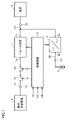
- FIG. 1 is a circuit block diagram showing a configuration of an uninterruptible power supply according to an embodiment of the present invention.
- this uninterruptible power supply includes an input terminal T1, an output terminal T2, a battery terminal T3, a plurality of (two in FIG. 1) vacuum circuit breakers (mechanical switches) S1, S2, a bypass circuit 1, and a power converter. 2 and a control device 3.
- the input terminal T1 receives the commercial frequency AC voltage VI supplied from the commercial AC power supply 4.
- the instantaneous value of the AC voltage VI is detected by the control device 3.
- the control device 3 detects a power failure and a power recovery of the commercial AC power supply 4 based on the detected value of the AC voltage VI.
- the output terminal T2 is connected to the load 5.
- the load 5 is driven by an AC voltage VO supplied from the output terminal T2 of the uninterruptible power supply.
- the instantaneous value of the AC voltage VO is detected by the control device 3.
- the battery terminal T3 is connected to the battery 6 (DC power supply, power storage device).
- the battery 6 stores DC power.
- a capacitor may be connected instead of the battery 6.
- the instantaneous value of the DC voltage VB (voltage between terminals of the battery 6) of the battery terminal T3 is detected by the control device 3.
- the other terminal 1b of the bypass circuit 1 is connected to the output terminal T2.
- the bypass circuit 1 is controlled by the control device 3. When the commercial AC power supply 4 is sound, the bypass circuit 1 is turned on. When the commercial AC power supply 4 fails, the bypass circuit 1 is turned off.
- the AC terminal 2a of the power converter 2 is connected to the output terminal T2, and the DC terminal 2b of the power converter 2 is connected to the battery terminal T3.
- the power converter 2 is controlled by the control device 3.
- the control device 3 controls the power converter 2 so that the voltage VB between the terminals of the battery 6 becomes the reference voltage VBR.
- the power converter 2 converts the DC power of the battery 6 into AC power of a commercial frequency and supplies it to the load 5.
- the control device 3 controls the power converter 2 so that the AC voltage VO of the output terminal T2 becomes the reference AC voltage VOR. Further, the control device 3 stops the operation of the power converter 2 when the voltage VB between the terminals of the battery 6 reaches the lower limit voltage.
- AC power is supplied from the commercial AC power supply 4 to the power converter 2 via the vacuum breakers S1 and S2 and the bypass circuit 1, and the AC power is converted into DC power by the power converter 2 and stored in the battery 6. ..
- a vacuum circuit breaker for example, S1 different from the vacuum circuit breaker (for example, S2) that was turned off at the time of the previous power failure is turned off, the bypass circuit 1 is turned off, and the commercial AC is turned off.
- the power supply 4 and the load 5 are cut off.
- the DC power of the battery 6 is converted into AC power by the power converter 2 and supplied to the load 5, and the operation of the load 5 is continued.
- the vacuum circuit breakers S1 and S2 and the bypass circuit 1 are both turned on, and AC power is supplied from the commercial AC power supply 4 to the load 5 via the vacuum circuit breakers S1 and S2 and the bypass circuit 1. , The load 5 is operated.
- AC power is supplied from the commercial AC power supply 4 to the power converter 2 via the vacuum breakers S1 and S2 and the bypass circuit 1, and the AC power is converted into DC power by the power converter 2 and stored in the battery 6. ..
- the vacuum circuit breaker S2 different from the vacuum circuit breaker S1 that was turned off at the time of the previous power failure is turned off, the bypass circuit 1 is turned off, and the space between the commercial AC power supply 4 and the load 5 is turned off. Is blocked.
- the DC power of the battery 6 is converted into AC power by the power converter 2 and supplied to the load 5, and the operation of the load 5 is continued.
- FIG. 2 is a block diagram showing the configuration of the vacuum breaker S1.
- the vacuum breaker S1 includes a vacuum valve 10, conductors 13, 14, external terminals 15, 16, an operation rod 17, an operation mechanism unit 18, a spring 19, and a drive unit 20.
- the vacuum valve 10 includes a pair of electrodes 11 and 12.
- the tips of the electrodes 11 and 12 are provided in the vacuum valve 10 and are arranged so as to face each other.
- the rear ends of the electrodes 11 and 12 are exposed to the outside of the vacuum valve 10.
- the electrode 11 is fixed to the upper end portion of the vacuum valve 10, and the electrode 12 is supported by the lower end portion of the vacuum valve 10 so as to be movable in the vertical direction.
- the rear end of the electrode 11 is connected to the external terminal 15 via the conductor 13.
- the rear end portion of the electrode 12 is connected to the external terminal 16 via the conductor 14 and is connected to the operation mechanism portion 18 via the operation rod 17.
- the operating rod 17 is made of an insulating material.
- the drive unit 20 includes a power storage motor, a cam, and the like, and stores the spring 19.
- the operation mechanism unit 18 moves the operation rod 17 downward in response to the off command signal S1off from the control device 3.
- the electrode 12 moves downward, the tips of the electrodes 11 and 12 are separated from each other, the external terminals 15 and 16 are in a non-conducting state, and the vacuum breaker S1 is turned off.
- the operation mechanism unit 18 releases the spring 19 in response to the on command signal S1on from the control device 3, and uses the release force of the spring 19 to release the operation rod 17. Move upwards.
- the operation rod 17 moves upward, the electrode 12 moves upward, the tips of the electrodes 11 and 12 come into contact with each other, the external terminals 15 and 16 are in a conductive state, and the vacuum breaker S1 is turned on.
- the drive unit 20 stores the spring 19 as soon as the spring 19 is released.
- FIG. 3 is a time chart illustrating the operation of the vacuum circuit breaker S1 when only one vacuum circuit breaker S1 is connected between the input terminal T1 and one terminal 1a of the bypass circuit 1.
- (A) shows the effective value of the AC voltage VI supplied from the commercial AC power supply 4
- (B) shows the on and off states of the vacuum circuit breaker S1
- (C) shows the energy E1 of the spring 19. Is shown.
- FIG. 3 shows a case where a power failure and a power recovery of the commercial AC power supply 4 are repeated.
- the AC voltage VI becomes high, and when the commercial AC power supply 4 fails, the AC voltage VI becomes low.
- the spring 19 When the spring 19 is released, the spring 19 is immediately stored by the drive unit 20 (FIG. 2). When the energy E1 of the spring 19 is started, the energy E1 of the spring 19 gradually increases. In order to increase the energy E1 of the spring 19 from a low value to a high value, a predetermined time Tc is required.
- the spring 19 is stored at t5 at the time of power recovery. Since the force is completed, the vacuum breaker S1 can be turned on at t5 at the time of power recovery.
- the vacuum breaker S1 cannot be turned on at t9 at the time of power recovery.
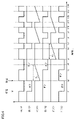
- FIG. 4 is a time chart illustrating the operation of the vacuum circuit breakers S1 and S1 when two vacuum circuit breakers S1 and S2 are connected between the input terminal T1 and one terminal 1a of the bypass circuit 1.
- (A) shows the effective value of the AC voltage VI supplied from the commercial AC power supply 4
- (B) shows the on and off states of the vacuum circuit breaker S1
- (C) shows the vacuum circuit breaker S1.
- the energy E1 of the spring 19 is shown
- D) shows the on and off states of the vacuum circuit breaker S2
- E shows the energy E2 of the spring 19 of the vacuum circuit breaker S2
- (F) is 2 connected in series.
- the on and off states of one mechanical switch S3 composed of one vacuum circuit breaker S1 and S2 are shown.
- FIG. 4 shows a case where a power failure and a power recovery of the commercial AC power supply 4 are repeated at the same timing as in FIG.
- the commercial AC power supply 4 is sound, the AC voltage VI becomes high, and when the commercial AC power supply 4 fails, the AC voltage VI becomes low.
- the commercial AC power supply 4 is sound, the vacuum circuit breakers S1 and S2 are both turned on, the energy E1 and E2 of the springs 19 of the vacuum circuit breakers S1 and S2 are set to high values, and the mechanical switch S3 is turned on. It is assumed that there is.
- the vacuum circuit breaker S1 different from the previously turned off vacuum circuit breaker S2 among the vacuum circuit breakers S1 and S2 is turned off, and the mechanical switch S3 is turned off.
- one vacuum circuit breaker for example, S1 is turned off and on, and the other vacuum circuit breaker is stored while the spring 19 of the vacuum circuit breaker S1 is stored.
- S2 is turned off and on (for example, times t6 to t10). Therefore, even when the time from power recovery to power failure and power recovery is shorter than the predetermined time Tc (for example, time t7 to t9), the vacuum breaker S2 can be turned on at power recovery t9.
- the mechanical switch S3 can be turned off at the time of the power failure and the mechanical switch S3 can be turned on at the time of the power recovery.
- the mechanical switches S3 (that is, the vacuum breakers S1 and S2) can be operated normally.
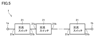
- FIG. 5 is a block diagram showing the configuration of the bypass circuit 1.
- the bypass circuit 1 includes a plurality of stages of AC switches 21 connected in series between one terminal 1a and the other terminal 1b.
- One terminal 21a of the first-stage AC switch 21 is connected to one terminal 1a of the bypass circuit 1.
- One terminal 21a of each AC switch 21 in the second and subsequent stages is connected to the other terminal 12b of the AC switch 21 in the previous stage, and the other terminal 21b of each AC switch 21 in the second and subsequent stages is one terminal 12a of the AC switch 21 in the subsequent stage.
- the other terminal 21b of the AC switch 21 in the final stage is connected to the other terminal 1b of the bypass circuit 1, that is, the output terminal T2 (FIG. 1).
- the plurality of AC switches 21 are controlled by the control device 3. When the commercial AC power supply 4 is sound, the plurality of AC switches 21 are turned on together and the bypass circuit 1 is turned on. When the commercial AC power supply 4 loses power, both of the plurality of AC switches 21 are turned off and the bypass circuit 1 is turned off.
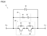
- FIG. 6 is a circuit diagram showing the configuration of the AC switch 21.
- the AC switch 21 includes a semiconductor switch 22, a snubber circuit 23, and a varistor 26 connected in parallel between one terminal 21a and the other terminal 21b.
- the semiconductor switch 22 includes the IGBT Q1 and Q2 and the diodes D1 and D2.
- the collectors of IGBT Q1 and Q2 are connected to each other, and their emitters are connected to terminals 21a and 21b, respectively.
- the diodes D1 and D2 are connected in antiparallel to the IGBT Q1 and Q2, respectively. Each on and off of the IGBT Q1 and Q2 is controlled by the control device 3.
- the gates of the IGBT Q1 and Q2 are set to the "L” level and the “H” level, respectively, during the period when the AC voltage VI supplied from the commercial AC power supply 4 is a positive voltage.
- the IGBT Q1 and Q2 are turned off and on, respectively, and a current flows from one terminal 21a to the other terminal 21b via the diode D1 and the IGBT Q2.
- the gates of the IGBT Q1 and Q2 are set to the "H" level and the "L” level, respectively, during the period when the AC voltage VI supplied from the commercial AC power supply 4 is a negative voltage. ..
- the IGBT Q1 and Q2 are turned on and off, respectively, and a current flows from the other terminal 21b to the one terminal 21a via the diode D2 and the IGBT Q1. Therefore, when the commercial AC power supply 4 is sound, the semiconductor switch 22 is turned on.
- the gates of the IGBT Q1 and Q2 are both set to the "L" level, and both the IGBT Q1 and Q2 are turned off. Therefore, when the commercial AC power supply 4 fails, the semiconductor switch 22 is turned off.
- Patent Document 1 there is also a method of configuring a bypass circuit by a pair of thyristors connected in antiparallel to each other.
- the thyristor is not turned off until the current flowing through the thyristor reaches 0 A, so that the cutoff time of the bypass circuit becomes long.
- the bypass circuit 1 is configured by using the semiconductor switch 22 including the IGBT Q1 and Q2 and the diodes D1 and D2, the cutoff time of the bypass circuit 1 can be shortened.
- this semiconductor switch 22 has a disadvantage that it is vulnerable to surge voltage as compared with a thyristor. Therefore, in the present embodiment, each of the snubber circuit 23 and the varistor 26 is connected in parallel to the semiconductor switch 22.
- the snubber circuit 23 includes a resistance element 24 and a capacitor 25 connected in series between the terminals 21a and 21b.
- the snubber circuit 23 protects the semiconductor switch 22 by suppressing such a surge voltage.
- the varistor 26 is connected between the terminals 21a and 21b.
- the resistance value of the varistor 26 becomes a high value.
- the resistance value of the varistor 26 becomes a low value. Therefore, it is possible to prevent the voltage between the terminals 21a and 21b from exceeding the threshold voltage and prevent the semiconductor switch 22 from being damaged by the surge voltage.
- the bypass circuit 1 is configured by using the semiconductor switch 22 including the IGBT Q1 and Q2 and the diodes D1 and D2, the commercial AC power supply 4 is compared with the case where the bypass circuit is configured by the pair of thyristors.
- the bypass circuit 1 can be quickly turned off, and the commercial AC power supply 4 and the load 5 can be cut off in a short time.
- each of the snubber circuit 23 and the varistor 26 is connected in parallel to the semiconductor switch 22, it is possible to prevent the semiconductor switch 22 from being destroyed by the surge voltage.
- the snubber circuit 23 including the resistance element 24 and the capacitor 25 connected in series transmits an AC voltage. Therefore, even when the semiconductor switch 22 is turned off when the commercial AC power supply 4 fails, the AC voltage VO generated by the power converter 2 (FIG. 1) is one of the bypass circuits 1 via the multi-stage snubber circuit 23. It is transmitted to the terminal 1a.
- the breaking time of the vacuum circuit breakers S1 and S2 is longer than the breaking time of the semiconductor switch 22, if the vacuum circuit breaker S1 or S2 is not turned off yet, the AC voltage generated by the power converter 2 is generated.
- the VO is transmitted to the input terminal T1 via the multi-stage snubber circuit 23 and the vacuum circuit breakers S1 and S2.
- the commercial AC power supply 4 is actually out of power, it is determined that the commercial AC power supply 4 has been restored based on the AC voltage VI of the input terminal T1, and the vacuum circuit breakers S1 and S2 and the bypass circuit 1 are determined. Is turned on, and the DC-AC conversion operation of the power converter 2 may be stopped. When the DC-AC conversion operation of the power converter 2 is stopped, the output of the AC voltage VO from the power converter 2 is stopped, and it is determined that the power failure of the commercial AC power supply 4 has occurred again.
- the control device 3 determines whether or not the commercial AC power supply 4 has been restored after a predetermined time Td has elapsed since the power failure of the commercial AC power supply 4 occurred.
- the predetermined time Td is set to a time longer than the cutoff time required to turn off each of the vacuum breakers S1 and S2.
- FIG. 7 is a block diagram showing the configuration of the control device 3.
- the control device 3 includes voltage detectors 30 to 32, a power failure detector 33, a power recovery detector 34, and a control unit 35.
- the voltage detector 30 detects an instantaneous value of the AC voltage VI of the input terminal T1 and outputs a signal ⁇ 30 indicating the detected value.
- the voltage detector 31 detects the instantaneous value of the AC voltage VO of the output terminal T2, and outputs a signal ⁇ 31 indicating the detected value.
- the voltage detector 32 detects an instantaneous value of the DC voltage VB of the battery terminal T3, and outputs a signal ⁇ 32 indicating the detected value.
- the power failure detector 33 compares the high and low of the effective value and the lower limit value of the AC voltage VI indicated by the output signal ⁇ 30 of the voltage detector 30, and outputs the power failure detection signal ⁇ 33 based on the comparison result.
- the power failure detection signal ⁇ 33 is set to the “H” level of the deactivation level.
- the power failure detection signal ⁇ 33 is set to the “L” level of the activation level.
- the power recovery detector 34 is of the AC voltage VI indicated by the output signal ⁇ 30 of the voltage detector 30 after a predetermined time Td has elapsed since the failure detection signal ⁇ 33 was lowered from the “H” level to the “L” level.
- the high and low values of the effective value and the lower limit value are compared, and the power recovery detection signal ⁇ 34 is output based on the comparison result.
- the power recovery detection signal ⁇ 34 is set to the “L” level of the deactivation level.
- the power recovery detection signal ⁇ 34 is set to the “H” level of the activation level.
- the control unit 35 sets the vacuum breakers S1 and S2, the bypass circuit 1, and the power converter 2 based on the output signals ⁇ 30 to ⁇ 32 of the voltage detectors 30 to 32, the power failure detection signal ⁇ 33, and the power recovery detection signal ⁇ 34. Control.
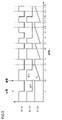
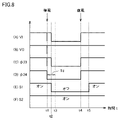
- FIG. 8 is a time chart showing the operation of the control device 3 shown in FIG. 7.
- (A) shows the effective value of the AC voltage VI of the input terminal T1
- (B) shows the effective value of the AC voltage VO of the output terminal T2
- (C) shows the waveform of the power failure detection signal ⁇ 33.
- (D) show the waveform of the power recovery detection signal ⁇ 34
- (E) show the on and off state of the vacuum circuit breaker S1
- (F) show the on and off state of the vacuum circuit breaker S2.
- FIG. 8 it is assumed that the commercial AC power supply 4 is sound and the vacuum circuit breakers S1 and S2 and the bypass circuit 1 are turned on in the initial state.
- the AC voltage VI is supplied from the commercial AC power supply 4 to the output terminal T2 via the vacuum circuit breakers S1 and S2 and the bypass circuit 1, and the AC voltages VI and VO are both set to high values.
- the power failure detection signal ⁇ 33 is set to the non-activation level “H” level
- the power recovery detection signal ⁇ 34 is set to the activation level “H” level.
- the power failure detection signal ⁇ 33 is set to the activation level “L” level, and the power recovery detection signal ⁇ 34. Is set to the "L" level of the deactivation level.
- the control unit 35 When the power failure detection signal ⁇ 33 is set to the activation level “L” level, the control unit 35 turns off each semiconductor switch 22 of the bypass circuit 1, and a vacuum different from the vacuum circuit breaker (S2) that was turned off last time.
- the off command signal S1off (FIG. 2) is output to the circuit breaker S1, and the power converter 2 is made to execute the DC-AC conversion operation.
- the vacuum breaker S1 starts the cutoff operation in response to the off command signal S1off, and turns off at the time t2 after the cutoff time has elapsed.
- the power converter 2 converts the DC voltage VB of the battery 6 into an AC voltage VO and outputs it to the output terminal T2 according to a command from the control unit 35. While this AC voltage VO is supplied to the load 5, it is transmitted to the input terminal T1 via the plurality of snubber circuits 23 (FIG. 6) included in the bypass circuit 1 and the vacuum circuit breakers S1 and S2, and the AC voltage VI.
- the voltage detector 30 detects the voltage, and the failure detection signal ⁇ 33 is set to the deactivation level “H” level (time t1 to t2).
- the power recovery detector 34 determines whether or not the commercial AC power supply 4 has recovered power based on the output signal ⁇ 30 of the voltage detector 30 within this period (time t1 to t2), the power is actually recovered. Even though there is no power, it is mistakenly recognized as having been restored. Therefore, the power recovery detector 34 of the present embodiment stops determining whether or not the power has been recovered during the period (time t1 to t3) from the power failure to the elapse of a predetermined time Td, and the power failure (time 1). ) At time t3 after a predetermined time Td has elapsed, the determination of whether or not the power has been restored is started. Since this predetermined time Td is longer than the shutoff time of the vacuum breaker S1, the vacuum breaker S1 is turned off at time t3.
- the vacuum circuit breaker S1 When the vacuum circuit breaker S1 is turned off (time t2), the AC output voltage VO of the power converter 2 is not transmitted to the input terminal T1, the AC voltage VI is reduced to a low value, and the power failure detection signal ⁇ 33 is set to the activation level “ It is set to the "L" level.
- the determination of whether or not the power is restored by the power recovery detector 34 is restarted, and the power recovery detection signal ⁇ 34 is maintained at the deactivation level “L” level.
- the AC voltage VI supplied from the commercial AC power supply 4 rises to a high value.
- the power failure detection signal ⁇ 33 is set to the deactivation level “H” level, and the power recovery detection signal ⁇ 34 is set to the activation level “H” level.
- the control unit 35 controls the power converter 2 so that the phase of the AC voltage VO matches the phase of the AC voltage VI.
- the control unit 35 turns on the bypass circuit 1 and outputs an on command signal S1on (FIG. 2) to the vacuum circuit breaker S1.
- the vacuum circuit breaker S1 is turned on (time t5), AC power is supplied from the commercial AC power supply 4 to the load 5 via the vacuum circuit breakers S1 and S2 and the bypass circuit 1.
- the control unit 35 causes the power converter 2 to perform an AC-DC conversion operation.
- the bypass circuit 1 is configured by using the semiconductor switch 22 including the IGBT Q1 and Q2 and the diodes D1 and D2, the bypass circuit 1 is configured by using a pair of thyristors, as compared with the case where the bypass circuit is configured by using a pair of thyristors.
- the bypass circuit 1 can be quickly cut off, and the commercial AC power supply 4 and the load 5 can be quickly disconnected.
- two vacuum circuit breakers S1 and S2 are connected in series between the input terminal T1 and one terminal 1a of the bypass circuit 1, and when the commercial AC power supply 4 is sound, both the two vacuum circuit breakers S1 and S2 are turned on.
- a vacuum circuit breaker (S2 in this case) different from the vacuum circuit breaker (for example, S1) that was turned off at the previous power failure is turned off. Therefore, in the event of a power failure of the commercial AC power supply 4, it is possible to prevent the AC output voltage of the power converter 2 from appearing at the input terminal T1 via the bypass circuit 1 and prevent the malfunction of the uninterruptible power supply device.
- the power converter 2 is used via the bypass circuit 1 and the vacuum circuit breakers S2 and S1. It is possible to prevent it from being mistakenly determined that the power has been restored by detecting the AC voltage supplied.
- the vacuum circuit breaker (S2 in this case) in which the spring 19 is already stored is turned off, so that it is a commercial AC power supply.
- the vacuum circuit breakers S1 and S2 can be quickly turned on.
- the inexpensive vacuum circuit breakers S1 and S2 are used without using the expensive high-speed mechanical switch, the cost of the device can be reduced. Therefore, it is possible to realize a low-priced uninterruptible power supply that operates at high speed and stably.
- N vacuum circuit breakers (N is an integer of 3 or more) may be connected in series with one terminal 1a of 1. In this case, when N times of power failure and power recovery occur, N vacuum circuit breakers may be turned off and on one by one.
- FIG. 9 is a circuit diagram showing a modified example of the embodiment, and is a diagram to be compared with FIG. With reference to FIG. 9, the difference between this modification and the embodiment is that the semiconductor switch 22 is replaced with the semiconductor switch 22A.
- the semiconductor switch 22A includes the IGBT Q1 and Q2 and the diodes D1 and D2.
- the emitters of IGBT Q1 and Q2 are connected to each other, and their collectors are connected to terminals 21a and 21b, respectively.
- the diodes D1 and D2 are connected in antiparallel to the IGBT Q1 and Q2, respectively.
- Each on and off of the IGBT Q1 and Q2 is controlled by the control device 3.
- the gates of the IGBT Q1 and Q2 are set to the "H” level and the “L” level, respectively, during the period when the AC voltage VI supplied from the commercial AC power supply 4 is a positive voltage.
- the IGBT Q1 and Q2 are turned on and off, respectively, and a current flows from one terminal 21a to the other terminal 21b via the IGBT Q1 and the diode D2.
- the gates of the IGBT Q1 and Q2 are set to the "L" level and the "H” level, respectively, during the period when the AC voltage VI supplied from the commercial AC power supply 4 is a negative voltage. ..
- the IGBT Q1 and Q2 are turned off and on, respectively, and a current flows from the other terminal 21b to the one terminal 21a via the IGBT Q2 and the diode D1. Therefore, when the commercial AC power supply 4 is sound, the semiconductor switch 22A is turned on.
- the gates of the IGBT Q1 and Q2 are both set to the "L" level, and both the IGBT Q1 and Q2 are turned off. Therefore, when the commercial AC power supply 4 fails, the semiconductor switch 22A is turned off.
Landscapes
- Engineering & Computer Science (AREA)
- Power Engineering (AREA)
- Business, Economics & Management (AREA)
- Emergency Management (AREA)
- Stand-By Power Supply Arrangements (AREA)
Abstract
Description
Claims (8)
- 交流電源から供給される交流電力を受ける入力端子と、
負荷に接続される出力端子と、
前記入力端子と前記出力端子との間に直列接続された複数の機械スイッチおよびバイパス回路と、
前記交流電源の健全時には、前記複数の機械スイッチおよび前記バイパス回路をともにオンさせ、前記交流電源の停電時には、前記複数の機械スイッチのうちの前回の停電時にオフさせた機械スイッチと異なる機械スイッチをオフさせるとともに前記バイパス回路をオフさせる制御装置と、
前記交流電源の停電時に、直流電源から供給される直流電力を交流電力に変換して前記出力端子に出力する電力変換器とを備える、電源装置。 - 前記機械スイッチの各々は真空遮断器である、請求項1に記載の電源装置。
- 前記真空遮断器は、
一対の電極と、
バネと、
前記バネを蓄勢する駆動部と、
前記真空遮断器をオフさせる場合には前記一対の電極を離間させ、前記真空遮断器をオンさせる場合には、前記バネの放勢力を用いて前記一対の電極を接触させる操作機構部とを含む、請求項2に記載の電源装置。 - 前記バイパス回路は、互いに並列接続された半導体スイッチおよびスナバ回路を含む、請求項1に記載の電源装置。
- 前記半導体スイッチは、第1および第2の端子と、第1および第2のトランジスタと、第1および第2のダイオードとを含み、
前記第1および第2のトランジスタの第1の電極は互いに接続され、
前記第1および第2のトランジスタの第2の電極はそれぞれ前記第1および第2の端子に接続され、
前記第1および第2のダイオードは、それぞれ前記第1および第2のトランジスタに対して逆並列に接続され、
前記スナバ回路は、前記第1および第2の端子間に接続される、請求項4に記載の電源装置。 - 前記スナバ回路は、直列接続された抵抗素子およびコンデンサを含む、請求項4に記載の電源装置。
- 前記制御装置は、
前記入力端子の交流電圧を検出する電圧検出器と、
前記電圧検出器によって検出された交流電圧が正常範囲内でない場合に停電検出信号を出力する停電検出器と、
前記停電検出器から前記停電検出信号が出力されてから予め定められた時間が経過し、かつ前記電圧検出器によって検出された交流電圧が正常範囲内である場合に復電検出信号を出力する復電検出器と、
前記停電検出信号に応答して、前記複数の機械スイッチのうちの前回の停電時にオフさせた機械スイッチと異なる機械スイッチをオフさせるとともに、前記バイパス回路をオフさせ、前記復電検出信号に応答して、前記複数の機械スイッチおよび前記バイパス回路をともにオンさせる制御部とを含み、
前記予め定められた時間は、前記機械スイッチの遮断時間よりも長い、請求項1に記載の電源装置。 - 前記直流電源は、直流電力を蓄える電力貯蔵装置を含み、
前記電力変換器は、前記交流電源の健全時には、前記交流電源から前記複数の機械スイッチおよび前記バイパス回路を介して供給される交流電力を直流電力に変換して前記電力貯蔵装置に蓄え、前記交流電源の停電時には、前記電力貯蔵装置の直流電力を交流電力に変換して前記出力端子に出力する、請求項1に記載の電源装置。
Priority Applications (5)
| Application Number | Priority Date | Filing Date | Title |
|---|---|---|---|
| KR1020227019407A KR102699856B1 (ko) | 2020-11-10 | 2020-11-10 | 전원 장치 |
| PCT/JP2020/041930 WO2022101985A1 (ja) | 2020-11-10 | 2020-11-10 | 電源装置 |
| US17/784,070 US12009694B2 (en) | 2020-11-10 | 2020-11-10 | Uninterruptible power supply using vacuum circuit breaker |
| CN202080085925.4A CN114788129A (zh) | 2020-11-10 | 2020-11-10 | 电源装置 |
| JP2021510251A JP6974652B1 (ja) | 2020-11-10 | 2020-11-10 | 電源装置 |
Applications Claiming Priority (1)
| Application Number | Priority Date | Filing Date | Title |
|---|---|---|---|
| PCT/JP2020/041930 WO2022101985A1 (ja) | 2020-11-10 | 2020-11-10 | 電源装置 |
Publications (1)
| Publication Number | Publication Date |
|---|---|
| WO2022101985A1 true WO2022101985A1 (ja) | 2022-05-19 |
Family
ID=78766784
Family Applications (1)
| Application Number | Title | Priority Date | Filing Date |
|---|---|---|---|
| PCT/JP2020/041930 Ceased WO2022101985A1 (ja) | 2020-11-10 | 2020-11-10 | 電源装置 |
Country Status (5)
| Country | Link |
|---|---|
| US (1) | US12009694B2 (ja) |
| JP (1) | JP6974652B1 (ja) |
| KR (1) | KR102699856B1 (ja) |
| CN (1) | CN114788129A (ja) |
| WO (1) | WO2022101985A1 (ja) |
Families Citing this family (2)
| Publication number | Priority date | Publication date | Assignee | Title |
|---|---|---|---|---|
| WO2023233540A1 (ja) * | 2022-05-31 | 2023-12-07 | 東芝三菱電機産業システム株式会社 | 無停電電源装置 |
| KR102824916B1 (ko) * | 2022-10-06 | 2025-06-24 | 가부시키가이샤 티마이크 | 전원 장치 |
Citations (4)
| Publication number | Priority date | Publication date | Assignee | Title |
|---|---|---|---|---|
| JPH0582367A (ja) * | 1991-09-19 | 1993-04-02 | Chubu Electric Power Co Inc | 変圧器負荷時タツプ切換制御装置 |
| JP2016143564A (ja) * | 2015-02-02 | 2016-08-08 | オムロン株式会社 | 継電ユニット、および継電回路の制御方法 |
| JP2017070046A (ja) * | 2015-09-29 | 2017-04-06 | 東芝三菱電機産業システム株式会社 | 無停電電源装置 |
| JP2018195472A (ja) * | 2017-05-18 | 2018-12-06 | 富士電機機器制御株式会社 | 遮断器の蓄勢装置 |
Family Cites Families (13)
| Publication number | Priority date | Publication date | Assignee | Title |
|---|---|---|---|---|
| JP2002218673A (ja) * | 2001-01-16 | 2002-08-02 | Toshiba Corp | 無停電電源装置 |
| JP2009136099A (ja) | 2007-11-30 | 2009-06-18 | Sanken Electric Co Ltd | 電力供給装置及びこれに使用可能な振幅及び位相判定回路装置 |
| US8957546B2 (en) * | 2012-07-10 | 2015-02-17 | Nixon Power Services, Llc | Electrical cogeneration system and method |
| CN102856137B (zh) | 2012-08-31 | 2014-12-31 | 胡俊兵 | 一种低压智能双电源转换开关 |
| US20170004948A1 (en) * | 2013-03-13 | 2017-01-05 | Google Inc. | Electrical circuit protector |
| CN103337851B (zh) * | 2013-07-04 | 2015-09-23 | 国家电网公司 | 一种半控型有源注入电流式高压直流断路器及其实现方法 |
| JP6014061B2 (ja) * | 2014-01-22 | 2016-10-25 | 東芝三菱電機産業システム株式会社 | 無停電電源システム |
| JP6049957B2 (ja) * | 2014-09-26 | 2016-12-21 | 三菱電機株式会社 | 直流遮断器 |
| US10276321B2 (en) * | 2015-04-06 | 2019-04-30 | Atom Power, Inc. | Dynamic coordination of protection devices in electrical distribution systems |
| CN107615615B (zh) * | 2015-06-02 | 2020-06-30 | 东芝三菱电机产业系统株式会社 | 不间断电源装置 |
| US11373831B2 (en) * | 2019-05-18 | 2022-06-28 | Amber Solutions, Inc. | Intelligent circuit breakers |
| US10825625B1 (en) * | 2019-06-07 | 2020-11-03 | Smart Wires Inc. | Kinetic actuator for vacuum interrupter |
| CN111525675A (zh) * | 2020-04-30 | 2020-08-11 | 广东电网有限责任公司东莞供电局 | 一种交直流切换供电电路、方法及断路器 |
-
2020
- 2020-11-10 KR KR1020227019407A patent/KR102699856B1/ko active Active
- 2020-11-10 US US17/784,070 patent/US12009694B2/en active Active
- 2020-11-10 JP JP2021510251A patent/JP6974652B1/ja active Active
- 2020-11-10 WO PCT/JP2020/041930 patent/WO2022101985A1/ja not_active Ceased
- 2020-11-10 CN CN202080085925.4A patent/CN114788129A/zh active Pending
Patent Citations (4)
| Publication number | Priority date | Publication date | Assignee | Title |
|---|---|---|---|---|
| JPH0582367A (ja) * | 1991-09-19 | 1993-04-02 | Chubu Electric Power Co Inc | 変圧器負荷時タツプ切換制御装置 |
| JP2016143564A (ja) * | 2015-02-02 | 2016-08-08 | オムロン株式会社 | 継電ユニット、および継電回路の制御方法 |
| JP2017070046A (ja) * | 2015-09-29 | 2017-04-06 | 東芝三菱電機産業システム株式会社 | 無停電電源装置 |
| JP2018195472A (ja) * | 2017-05-18 | 2018-12-06 | 富士電機機器制御株式会社 | 遮断器の蓄勢装置 |
Also Published As
| Publication number | Publication date |
|---|---|
| JPWO2022101985A1 (ja) | 2022-05-19 |
| US12009694B2 (en) | 2024-06-11 |
| CN114788129A (zh) | 2022-07-22 |
| US20230039409A1 (en) | 2023-02-09 |
| KR20220098203A (ko) | 2022-07-11 |
| KR102699856B1 (ko) | 2024-08-27 |
| JP6974652B1 (ja) | 2021-12-01 |
Similar Documents
| Publication | Publication Date | Title |
|---|---|---|
| US11043837B2 (en) | Input power supply selection circuit | |
| JP6366711B2 (ja) | 電力変換装置 | |
| JP6567197B2 (ja) | 電力変換装置 | |
| JP2013110960A (ja) | 変換器を操作する方法とスイッチングセルと変換器 | |
| US9712042B2 (en) | Bypass apparatus for converter | |
| JP6183460B2 (ja) | インバータ装置 | |
| JP6974652B1 (ja) | 電源装置 | |
| WO2015097868A1 (ja) | 電力変換装置 | |
| EP3107200B1 (en) | Inverter grid-connected system and method for implementing three-phase alternating current grid-connected transition | |
| US20250046533A1 (en) | Power supply device | |
| CN111756232A (zh) | 功率单元 | |
| KR102171603B1 (ko) | 바이패스 스위치를 구비한 전력용 컨버터의 서브모듈 | |
| KR102177141B1 (ko) | 바이패스 스위치를 구비한 전력용 컨버터의 서브모듈 | |
| US10630068B2 (en) | System and switch assembly thereof with fault protection and associated method | |
| WO2019155522A1 (ja) | 電力変換装置 | |
| KR102552562B1 (ko) | 2개의 dc 그리드들을 커플링하기 위한 디바이스 및 방법 | |
| EP4411772B1 (en) | Dc circuit breaker | |
| WO2022158052A1 (ja) | ゲート駆動回路および電力変換装置 | |
| JP2019213445A (ja) | 電圧駆動型半導体スイッチング素子のゲート駆動装置、該ゲート駆動装置を備える電力変換装置 | |
| JP7580656B1 (ja) | 電力変換装置 | |
| JP2703140B2 (ja) | しや断器操作制御回路 | |
| JP2025180263A (ja) | 電力変換システム | |
| JP6406691B2 (ja) | 電磁石用電源装置 | |
| JPH04295226A (ja) | 電気供給装置 | |
| HK40005179A (en) | Discharge circuit for capacitor |
Legal Events
| Date | Code | Title | Description |
|---|---|---|---|
| ENP | Entry into the national phase |
Ref document number: 2021510251 Country of ref document: JP Kind code of ref document: A |
|
| ENP | Entry into the national phase |
Ref document number: 20227019407 Country of ref document: KR Kind code of ref document: A |
|
| 121 | Ep: the epo has been informed by wipo that ep was designated in this application |
Ref document number: 20961513 Country of ref document: EP Kind code of ref document: A1 |
|
| NENP | Non-entry into the national phase |
Ref country code: DE |
|
| 122 | Ep: pct application non-entry in european phase |
Ref document number: 20961513 Country of ref document: EP Kind code of ref document: A1 |