WO2022085511A1 - Inductor and method for manufacturing inductor - Google Patents
Inductor and method for manufacturing inductor Download PDFInfo
- Publication number
- WO2022085511A1 WO2022085511A1 PCT/JP2021/037682 JP2021037682W WO2022085511A1 WO 2022085511 A1 WO2022085511 A1 WO 2022085511A1 JP 2021037682 W JP2021037682 W JP 2021037682W WO 2022085511 A1 WO2022085511 A1 WO 2022085511A1
- Authority
- WO
- WIPO (PCT)
- Prior art keywords
- lead
- exterior member
- recess
- inductor
- out portion
- Prior art date
Links
- 238000004519 manufacturing process Methods 0.000 title claims description 25
- 238000000034 method Methods 0.000 title claims description 15
- 238000000748 compression moulding Methods 0.000 claims description 34
- 229910052751 metal Inorganic materials 0.000 claims description 31
- 239000002184 metal Substances 0.000 claims description 31
- 239000000696 magnetic material Substances 0.000 claims description 16
- 238000000465 moulding Methods 0.000 claims description 13
- 230000006835 compression Effects 0.000 claims description 10
- 238000007906 compression Methods 0.000 claims description 10
- 238000004804 winding Methods 0.000 claims description 10
- 238000005452 bending Methods 0.000 claims description 8
- 238000003825 pressing Methods 0.000 claims description 5
- 239000007769 metal material Substances 0.000 claims description 4
- 230000007423 decrease Effects 0.000 description 15
- 238000010586 diagram Methods 0.000 description 8
- 229910000679 solder Inorganic materials 0.000 description 7
- 239000000463 material Substances 0.000 description 6
- RYGMFSIKBFXOCR-UHFFFAOYSA-N Copper Chemical compound [Cu] RYGMFSIKBFXOCR-UHFFFAOYSA-N 0.000 description 2
- 230000000052 comparative effect Effects 0.000 description 2
- 238000005520 cutting process Methods 0.000 description 2
- 238000009795 derivation Methods 0.000 description 2
- 239000006247 magnetic powder Substances 0.000 description 2
- 239000002245 particle Substances 0.000 description 2
- 239000011347 resin Substances 0.000 description 2
- 229920005989 resin Polymers 0.000 description 2
- 229910017082 Fe-Si Inorganic materials 0.000 description 1
- 229910017133 Fe—Si Inorganic materials 0.000 description 1
- BQCADISMDOOEFD-UHFFFAOYSA-N Silver Chemical compound [Ag] BQCADISMDOOEFD-UHFFFAOYSA-N 0.000 description 1
- 229910002796 Si–Al Inorganic materials 0.000 description 1
- 229910008458 Si—Cr Inorganic materials 0.000 description 1
- 229910045601 alloy Inorganic materials 0.000 description 1
- 239000000956 alloy Substances 0.000 description 1
- 229910052782 aluminium Inorganic materials 0.000 description 1
- XAGFODPZIPBFFR-UHFFFAOYSA-N aluminium Chemical compound [Al] XAGFODPZIPBFFR-UHFFFAOYSA-N 0.000 description 1
- 239000004020 conductor Substances 0.000 description 1
- 229910052802 copper Inorganic materials 0.000 description 1
- 239000010949 copper Substances 0.000 description 1
- 239000000428 dust Substances 0.000 description 1
- 230000000694 effects Effects 0.000 description 1
- PCHJSUWPFVWCPO-UHFFFAOYSA-N gold Chemical compound [Au] PCHJSUWPFVWCPO-UHFFFAOYSA-N 0.000 description 1
- 229910052737 gold Inorganic materials 0.000 description 1
- 239000010931 gold Substances 0.000 description 1
- 238000009499 grossing Methods 0.000 description 1
- 238000001746 injection moulding Methods 0.000 description 1
- 239000002905 metal composite material Substances 0.000 description 1
- 239000000203 mixture Substances 0.000 description 1
- 238000012986 modification Methods 0.000 description 1
- 230000004048 modification Effects 0.000 description 1
- 239000011236 particulate material Substances 0.000 description 1
- 238000007747 plating Methods 0.000 description 1
- 229920001296 polysiloxane Polymers 0.000 description 1
- 239000000843 powder Substances 0.000 description 1
- 229910052709 silver Inorganic materials 0.000 description 1
- 239000004332 silver Substances 0.000 description 1
- 239000000126 substance Substances 0.000 description 1
- 229920001187 thermosetting polymer Polymers 0.000 description 1
- 238000001721 transfer moulding Methods 0.000 description 1
- 229910000859 α-Fe Inorganic materials 0.000 description 1
Images


Classifications
-
- H—ELECTRICITY
- H01—ELECTRIC ELEMENTS
- H01F—MAGNETS; INDUCTANCES; TRANSFORMERS; SELECTION OF MATERIALS FOR THEIR MAGNETIC PROPERTIES
- H01F17/00—Fixed inductances of the signal type
- H01F17/04—Fixed inductances of the signal type with magnetic core
-
- H—ELECTRICITY
- H01—ELECTRIC ELEMENTS
- H01F—MAGNETS; INDUCTANCES; TRANSFORMERS; SELECTION OF MATERIALS FOR THEIR MAGNETIC PROPERTIES
- H01F27/00—Details of transformers or inductances, in general
- H01F27/28—Coils; Windings; Conductive connections
- H01F27/29—Terminals; Tapping arrangements for signal inductances
- H01F27/292—Surface mounted devices
-
- H—ELECTRICITY
- H01—ELECTRIC ELEMENTS
- H01F—MAGNETS; INDUCTANCES; TRANSFORMERS; SELECTION OF MATERIALS FOR THEIR MAGNETIC PROPERTIES
- H01F27/00—Details of transformers or inductances, in general
- H01F27/24—Magnetic cores
- H01F27/255—Magnetic cores made from particles
-
- H—ELECTRICITY
- H01—ELECTRIC ELEMENTS
- H01F—MAGNETS; INDUCTANCES; TRANSFORMERS; SELECTION OF MATERIALS FOR THEIR MAGNETIC PROPERTIES
- H01F27/00—Details of transformers or inductances, in general
- H01F27/28—Coils; Windings; Conductive connections
- H01F27/2823—Wires
- H01F27/2828—Construction of conductive connections, of leads
-
- H—ELECTRICITY
- H01—ELECTRIC ELEMENTS
- H01F—MAGNETS; INDUCTANCES; TRANSFORMERS; SELECTION OF MATERIALS FOR THEIR MAGNETIC PROPERTIES
- H01F27/00—Details of transformers or inductances, in general
- H01F27/28—Coils; Windings; Conductive connections
- H01F27/2847—Sheets; Strips
- H01F27/2852—Construction of conductive connections, of leads
-
- H—ELECTRICITY
- H01—ELECTRIC ELEMENTS
- H01F—MAGNETS; INDUCTANCES; TRANSFORMERS; SELECTION OF MATERIALS FOR THEIR MAGNETIC PROPERTIES
- H01F41/00—Apparatus or processes specially adapted for manufacturing or assembling magnets, inductances or transformers; Apparatus or processes specially adapted for manufacturing materials characterised by their magnetic properties
- H01F41/02—Apparatus or processes specially adapted for manufacturing or assembling magnets, inductances or transformers; Apparatus or processes specially adapted for manufacturing materials characterised by their magnetic properties for manufacturing cores, coils, or magnets
- H01F41/0206—Manufacturing of magnetic cores by mechanical means
- H01F41/0246—Manufacturing of magnetic circuits by moulding or by pressing powder
-
- H—ELECTRICITY
- H01—ELECTRIC ELEMENTS
- H01F—MAGNETS; INDUCTANCES; TRANSFORMERS; SELECTION OF MATERIALS FOR THEIR MAGNETIC PROPERTIES
- H01F41/00—Apparatus or processes specially adapted for manufacturing or assembling magnets, inductances or transformers; Apparatus or processes specially adapted for manufacturing materials characterised by their magnetic properties
- H01F41/02—Apparatus or processes specially adapted for manufacturing or assembling magnets, inductances or transformers; Apparatus or processes specially adapted for manufacturing materials characterised by their magnetic properties for manufacturing cores, coils, or magnets
- H01F41/04—Apparatus or processes specially adapted for manufacturing or assembling magnets, inductances or transformers; Apparatus or processes specially adapted for manufacturing materials characterised by their magnetic properties for manufacturing cores, coils, or magnets for manufacturing coils
- H01F41/10—Connecting leads to windings
-
- H—ELECTRICITY
- H01—ELECTRIC ELEMENTS
- H01F—MAGNETS; INDUCTANCES; TRANSFORMERS; SELECTION OF MATERIALS FOR THEIR MAGNETIC PROPERTIES
- H01F17/00—Fixed inductances of the signal type
- H01F17/04—Fixed inductances of the signal type with magnetic core
- H01F2017/048—Fixed inductances of the signal type with magnetic core with encapsulating core, e.g. made of resin and magnetic powder
Definitions
- This disclosure relates to an inductor and a method for manufacturing an inductor.
- Patent Document 1 discloses an inductor including a coil portion, a plurality of exterior members surrounding the coil portion, and a terminal electrode portion connected to the coil portion and pulled out to the bottom surface of the exterior member.
- the magnetic saturation current may decrease depending on the shape of the exterior member. It is an object of the present disclosure to provide an inductor capable of suppressing a decrease in magnetic saturation current.
- the method for manufacturing an inductor is an inductor that includes a magnetic material and includes an exterior member having a bottom surface and a side surface connected to the bottom surface, and an energizing member partially covered by the exterior member.
- a lead-out portion and a terminal electrode portion having a flat shape thinner than the main body portion are formed on both outer sides of the main body portion of the metal wire.
- the exterior member is formed by compression molding the magnetic material so as to cover the main body portion and the lead-out portion and not to cover the terminal electrode portion by using the energizing member forming step to be formed and the molding die.
- a compression molding step of forming a recess connected to the bottom surface on the side surface of the exterior member, and the terminal electrode portion are aligned from the bottom surface of the exterior member toward the recess and further accommodated in the recess. Includes a folding step and a folding process.
- the inductor and the like of the present disclosure it is possible to suppress a decrease in the magnetic saturation current.
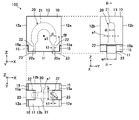
- FIG. 1 is a cross-sectional view of an inductor of a comparative example.
- FIG. 2 is a front view, a side view, and a bottom view of the inductor according to the embodiment.
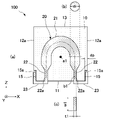
- FIG. 3 is a cross-sectional view of the inductor according to the embodiment.
- FIG. 4 is a cross-sectional view showing another example of the inductor according to the embodiment.
- FIG. 5 is a flowchart showing a method of manufacturing an inductor according to an embodiment.
- FIG. 6 is a diagram illustrating a current-carrying member forming step among the methods for manufacturing an inductor according to the embodiment.
- FIG. 7 is a diagram illustrating a coil portion forming step in the inductor manufacturing method according to the embodiment.
- FIG. 1 is a cross-sectional view of an inductor of a comparative example.
- FIG. 2 is a front view, a side view, and a bottom view of the inductor according to the embodiment.
- FIG. 8 is a diagram illustrating a compression molding process among the methods for manufacturing an inductor according to the embodiment.
- FIG. 9 is a diagram illustrating a bending process among the methods for manufacturing an inductor according to the embodiment.
- FIG. 10 is a cross-sectional view of the inductor of another embodiment.
- FIG. 1 is a cross-sectional view of the inductor 500 of the comparative example.
- the inductor 500 shown in FIG. 1A is similar to the inductor of Patent Document 1, and includes a coil portion 521, an exterior member 510 surrounding the coil portion 521, and a terminal electrode portion 523 connected to the coil portion 521. , Is equipped.
- the terminal electrode portion 523 is formed so as to extend along the bottom surface 511 of the exterior member 510 toward the outer side surface 512 of the exterior member 510.
- the terminal electrode portion 523 exposed from the exterior member 510 is formed only on the bottom surface 511 side of the exterior member 510. Therefore, when the inductor 500 is mounted on the circuit board, there is a problem that the fillet by solder cannot be sufficiently formed and the connection strength of the inductor 500 to the circuit board cannot be secured.
- the length of the metal plate constituting the terminal electrode portion 523 is lengthened, and the metal plate is bent so as to be in contact with the side surface 512 from the bottom surface 511 side, and the side surface is formed. It is conceivable that the terminal electrode portion 523 is also formed on the 512. According to this, a fillet made of solder can be formed by using the terminal electrode portion 523 formed on the side surface 512, and the connection strength of the inductor 500 to the circuit board can be secured.
- the terminal electrode portion 523 is provided on the side surface 512 of the exterior member 510, there is a problem that the mounting area of the inductor 500 becomes larger due to the increase in the thickness of the terminal electrode portion 523.
- the inductor of the present disclosure has the following configuration in order to suppress a decrease in the magnetic saturation current.
- each figure shows an X-axis, a Y-axis, and a Z-axis which mean three directions orthogonal to each other, and these axes are used for explanation as necessary.
- Each axis is provided for illustration purposes only and does not limit the direction and orientation in which the inductor is used.
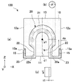
- FIG. 2 is a front view, a side view, and a bottom view of the inductor 100 according to the embodiment.
- 3A and 3B are cross-sectional views of the inductor 100, FIG. 3A is a cross-sectional view taken along the line iii-iii of FIG. 2, FIG. 3B is a cross-sectional view of the wire rod of the coil portion 21, and FIG. (C) is a cross-sectional view of the lead-out unit 22.
- the inductor 100 includes an exterior member 10 and an energizing member 20 partially covered by the exterior member 10.
- the inductor 100 is, for example, a rectangular parallelepiped metal composite, and its approximate outer shape is determined by the shape of the exterior member 10.
- the exterior member 10 can be formed into an arbitrary shape by molding. That is, the inductor 100 having an arbitrary shape can be realized depending on the shape of the exterior member 10 at the time of molding.
- the inductor 100 of the present embodiment has a dimension in the X-axis direction along the X-axis of 9 mm or more and 10 mm or less, a dimension in the Y-axis direction along the Y-axis of 4.4 mm or more and 6 mm or less, and a dimension in the Z-axis direction along the Z-axis. Is composed of an exterior member 10 having a size of 6 mm or more and 10 mm or less.
- the exterior member 10 is an outer shell portion of the inductor 100 and covers a part of the energizing member 20.
- the exterior member 10 is, for example, a dust core made of a metal magnetic powder, a resin material, or the like.
- the exterior member 10 may be formed by using a magnetic material, ferrite or the like may be used, or may be other than that.
- a particulate material having a predetermined elemental composition such as Fe—Si—Al system, Fe—Si system, Fe—Si—Cr system, or Fe—Si—Cr—B system is used.
- the resin material a material that can maintain a certain shape by binding the particles of the metallic magnetic material powder such as silicone while insulating the particles is selected.
- the energizing member 20 includes a coil portion 21, a plurality of lead-out portions 22 connected to both ends of the coil portion 21, and a plurality of terminal electrode portions 23 connected to each of the plurality of lead-out portions 22. are doing.
- the energizing member 20 of the present embodiment is composed of one coil portion 21, two lead-out portions 22, and two terminal electrode portions 23.
- the energizing member 20 is realized by a material selected from a metal material such as aluminum, copper, silver, and gold, and an alloy composed of a metal and another substance.
- the coil portion 21, the lead-out portion 22, and the terminal electrode portion 23 are names given to each portion formed by processing one member made of the same material. Hereinafter, each part will be described in the order of the terminal electrode portion 23, the coil portion 21, and the lead-out portion 22.
- the lead-out portion 22 is located between the two recesses 15 in the X-axis direction, and at least a part thereof faces the recess 15 of the exterior member 10. Specifically, the lead-out portion 22 is provided on the axis b1 of the energizing member 20 and has a lead-out portion flat surface 22a facing the concave portion flat surface 15a of the concave portion 15. Further, the lead-out unit 22 has a thickness in a direction perpendicular to the side surface 12a, that is, in the X-axis direction, and has a width in a direction parallel to both the side surface 12a and the bottom surface 11, that is, in the Y-axis direction. The lead-out unit 22 has a flat shape or a plate shape. For example, the width w1 of the lead-out unit 22 is 5 times or more and 10 times or less the thickness t1 of the lead-out unit 22.
- the thickness t1 of the lead-out portion 22 is smaller than the wire diameter di of the wire rod of the coil portion 21 (t1 ⁇ di). Further, the width w1 of the lead-out portion 22 is larger than the wire diameter di of the wire rod of the coil portion 21 (w1> di).
- the wire diameter di of the wire rod of the coil portion 21 is appropriately selected from the range of 1.3 mm or more and 1.8 mm or less, the thickness t1 of the lead-out portion 22 is 0.4 mm, and the width w1 is 2.5 mm.
- the amount of decrease in the thickness of the lead-out portion 22 with respect to the coil portion 21 is larger than the amount of decrease in the wall thickness of the exterior member 10 in the recess 15.
- T / 2 is 0.45 mm or more and 0.7 mm or less
- the depth dp of the recess 15 is 0.3 mm.
- the thickness t1 of the lead-out portion 22 is smaller than the wire diameter di of the wire rod of the coil portion 21. According to this configuration, the wall thickness of the exterior member 10 between the lead-out portion 22 and the recess 15 can be prevented from becoming unnecessarily thin. As a result, it is possible to suppress the occurrence of magnetic saturation in the exterior member 10 between the lead-out portion 22 and the recess 15.
- the cross section of the wire rod of the coil portion 21 is circular in the above, the cross section may be square (see FIG. 4).
- FIG. 4A and 4B are cross-sectional views showing another example of the inductor 100 according to the embodiment, FIG. 4A is a cross-sectional view of the inductor 100 seen from the Y-axis direction, and FIG. 4B is a coil.
- a cross-sectional view of the wire rod of the portion 21, FIG. 4 (c) is a cross-sectional view of the lead-out portion 22.
- the lead-out portion 22 and the coil portion 21 have the same dimensional relationship. Specifically, the thickness t1 of the lead-out portion 22 is thinner than the thickness t2 of the wire rod of the coil portion 21 (t1 ⁇ t2), and the width w1 of the lead-out portion 22 is wider than the width w2 of the wire rod of the coil portion 21. It may be good (w1> w2).
- FIG. 5 is a flowchart showing a manufacturing method of the inductor 100 according to the embodiment.
- the method for manufacturing the inductor 100 includes an energizing member forming step S101, a coil portion forming step S102, a compression forming step S103, and a bending step S104.
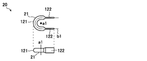
- FIG. 6 is a diagram illustrating a current-carrying member forming step S101 among the manufacturing methods of the inductor 100.
- FIG. 6A shows the metal wire 120 before press working
- FIGS. 6B and 6C show the energizing member 20 formed by pressing the metal wire 120. It is shown.
- the energizing member forming step S101 is a step of forming the energizing member 20 integrally including the coil portion 21, the lead-out portion 22, and the terminal electrode portion 23 from the metal wire 120.
- the metal wire 120 is a single copper wire extending in the axis b1 direction, and has a circular cross section (see (a) in FIG. 6).
- both ends of the metal wire 120 are press-processed using a press die (not shown).
- flat portions 122 having a flat surface 122a are formed on both outer sides of the main body portion 121 of the metal wire 120 (see (b) in FIG. 6).
- the main body portion 121 is a portion corresponding to the coil portion 21, and the flat portion 122 is a portion corresponding to the lead-out portion 22 and the terminal electrode portion 23.
- the flat portion 122 is formed on the axis b1 of the metal wire 120 by crushing the metal wire 120 from above and below.
- the flat portion 122 is processed so that the thickness t1 of the flat portion 122 is smaller than the wire diameter di of the main body portion 121.
- the axis b1 of the metal wire 120 is the same as the axis b1 of the energizing member 20.
- the crushed flat portion 122 is cut on three sides on the outer circumference, and the dimensions in the width direction and the axis b1 direction (longitudinal direction) are adjusted (see (c) in FIG. 6).
- the width w1 of the flat portion 122 after cutting is larger than the wire diameter di of the main body portion 121.
- FIG. 7 is a diagram illustrating the coil portion forming step S102 in the manufacturing method of the inductor 100.
- the coil portion 21 is formed by winding the center of the energizing member 20, that is, the main body portion 121 of the metal wire 120.
- the coil portion 21 is formed by winding the main body portion 121 in a U shape for 0.5 turn. After winding, the flat portions 122 connected to both ends of the coil portion 21 face each other.
- FIG. 8 is a diagram illustrating the compression molding step S103 among the manufacturing methods of the inductor 100.
- a magnetic material is compression-molded using a molding die (not shown).
- the exterior member is formed by covering the entire body portion 121 and a part of the flat portion 122 with a magnetic material, and compression-molding the other parts except a part of the flat portion 122 so as not to be covered with the magnetic material.
- a part of the flat portion 122 covered with the exterior member 10 becomes the lead-out portion 22, and the other portion of the flat portion 122 not covered with the exterior member 10 becomes the terminal electrode portion 23.
- a recess 15 connected to the bottom surface 11 is formed on the side surface 12a of the exterior member 10.
- the concave portion 15 is formed by providing a convex portion protruding inward on the inner wall of the molding die.
- compression molding is performed with the coil portion 21 arranged in the molding die so that the winding shaft a1 of the coil portion 21 is aligned with the compression direction P1 of the compression molding.
- the plane 122a of the flat portion 122 that is, the plane of the lead-out portion 22 (the plane of the lead-out portion 22a) is along the compression direction P1 of the compression molding, and more specifically, the width direction of the lead-out portion 22 is along the compression direction P1.
- compression molding is performed with the lead-out portion 22 arranged in the molding die.
- the pressing force during compression molding is, for example, 5 ton / cm 2
- the thermosetting temperature is, for example, 185 ° C.
- the compression molding may be injection molding or transfer molding.
- the exposed terminal electrode portion 23 which is not covered by the exterior member 10, protrudes perpendicularly to the bottom surface 11 of the exterior member 10.
- the terminal electrode portion 23 is subjected to solder plating or the like, if necessary.
- FIG. 9 is a diagram illustrating the bending step S104 in the manufacturing method of the inductor 100.
- the terminal electrode portion 23 is bent at a right angle toward the bottom surface 11, and the terminal electrode portion 23 is aligned from the bottom surface 11 of the exterior member 10 toward the recess 15.
- the terminal electrode portion 23 of the remaining portion excluding the portion along the bottom surface 11 is bent at a right angle so as to be accommodated in the recess 15, and is accommodated in the recess 15.
- the terminal electrode portion 23 is provided on the side surface 12a side of the inductor 100.
- the inductor 100 is manufactured by the energizing member forming step S101, the coil portion forming step S102, the compression molding step S103, and the bending step S104.
- the inductor 100 contains a magnetic material, an exterior member 10 having a bottom surface 11 and a side surface 12a connected to the bottom surface 11, and a metal material, and is partially covered by the exterior member 10.
- the energizing member 20 is provided.
- the energizing member 20 is connected to a coil portion 21 covered with an exterior member 10, a lead-out portion 22 connected to both ends of the coil portion 21 and extending toward the bottom surface 11 while being covered with the exterior member 10, and a lead-out portion 22. It has a terminal electrode portion 23 exposed from the bottom surface 11 of the exterior member 10.
- the wall thickness of the exterior member 10 between the lead-out portion 22 and the recess 15 becomes larger than necessary. It can suppress thinning. As a result, it is possible to suppress the occurrence of magnetic saturation in the exterior member 10 between the lead-out portion 22 and the recess 15, and it is possible to suppress the decrease in the magnetic saturation current of the inductor 100. Further, by providing the recess 15 on the side surface 12a of the exterior member 10 and accommodating a part of the terminal electrode portion 23 in the recess 15, it is possible to suppress the expansion of the mounting area of the inductor 100.
- terminal electrode portion 23 not only in the bottom surface 11 but also in the recess 15 on the side surface 12a, for example, when the inductor 100 is mounted on a circuit board, a fillet made of solder can be formed. This makes it possible to secure the connection strength of the inductor 100 to the circuit board.
- out-licensing unit 22 may have a flat shape.
- the lead-out portion 22 has a flat shape, it is possible to secure the wall thickness of the exterior member 10 between the lead-out portion 22 and the recess 15. As a result, it is possible to suppress the occurrence of magnetic saturation in the exterior member 10 between the lead-out portion 22 and the recess 15, and it is possible to suppress the decrease in the magnetic saturation current of the inductor 100.
- the recess 15 may have a recess plane 15a parallel to the side surface 12a, and the lead-out portion 22 may have a lead-out plane 22a facing the recess plane 15a.
- the lead-out portion 22 has a thickness in a direction perpendicular to the side surface 12a, the difference between the thickness t1 of the lead-out portion 22 and the wire diameter di or the thickness t2 of the wire rod of the coil portion 21 is T, and the recess 15 is the side surface 12a.
- T / 2 ⁇ dp may be satisfied.
- the width w1 of the lead-out portion 22 may be larger than the wire diameter di or the width w2 of the wire rod of the coil portion 21.
- the cross-sectional area of the lead-out unit 22 can be increased as compared with the case where the width w1 is the same as the wire diameter di or the width w2.
- the DC resistance loss in the lead-out unit 22 can be suppressed, and the decrease in the inductance value of the inductor 100 can be suppressed.
- the aspect ratio of the cross section of the wire rod of the coil portion 21 may be 1: 1.
- the magnetic path length can be shortened and the magnetic efficiency can be improved as compared with the coil portion 21 having a plate-shaped cross section of the wire rod.
- the exterior member is formed by compression molding the magnetic material so as to cover the main body 121 and the lead-out portion 22 and not to cover the terminal electrode portion 23 by using the current-carrying member forming step S101 for forming the terminal electrode portion 23 and the molding die.
- the compression molding step S103 for forming the recess 15 connected to the bottom surface 11 on the side surface 12a of the exterior member 10 and the terminal electrode portion 23 are aligned from the bottom surface 11 of the exterior member 10 toward the recess 15, and further.
- the bending step S104 which is bent so as to be accommodated in the recess 15, is included.
- compression molding may be performed with the lead-out portion 22 arranged in the molding die so that the flat surface of the flat-shaped lead-out portion 22 follows the compression direction P1 of the compression molding.
- the magnetic material easily flows along the lead-out portion 22, and the density of the exterior member 10 after compression molding can be increased. As a result, magnetic saturation is less likely to occur in the exterior member 10, and it is possible to suppress a decrease in the magnetic saturation current of the inductor 100.
- the coil portion 21 is formed by winding the main body portion 121 of the metal wire 120 for 0.5 turn or more and less than 1.0 turn before the compression forming step S103.
- compression molding step S103 including the forming step S102 compression molding is performed in a state where the coil portion 21 is arranged in the molding die so that the winding shaft a1 of the coil portion 21 follows the compression direction P1 of the compression molding. May be good.
- the magnetic material easily enters the inside of the coil portion 21, and the density of the exterior member 10 after compression molding can be increased. As a result, magnetic saturation is less likely to occur in the exterior member 10, and it is possible to suppress a decrease in the magnetic saturation current of the inductor 100.
- an electric product or an electric circuit using the above-mentioned inductor is also included in the present disclosure.
- the electric product include a power supply device provided with the above-mentioned inductor.
- the flat portion 122 is formed on the axis b1 of the metal wire 120 is shown, but the present invention is not limited to this, and the flat portion 122 may be formed at a position deviating from the axis b1 of the metal wire 120. ..
- the flat portion 122 can be formed so as to be biased downward. That is, the lead-out portion 22 does not necessarily have to be provided on the axis b1 of the energizing member 20, and as shown in FIG. 10, the lead-out portion 22 is closer to the inside of the exterior member 10 than the axis b1, that is, the center of the exterior member 10.
- the inductor 100 is configured such that the difference T between the thickness t1 of the lead-out portion 22 and the wire diameter di of the wire rod of the coil portion 21 is equal to or greater than the depth dp of the recess 15 (T ⁇ dp). good.
Abstract
Description
前述したように、近年、電子機器で使用される電流が大きくなり、インダクタの磁気飽和電流を高くすることが求められている。一方で、インダクタが実装される回路基板では、インダクタの取り付け面積を小さくし、また、回路基板に対するインダクタの接続強度を確保することが求められている。 (Background to this disclosure)
As described above, in recent years, the current used in electronic devices has increased, and it has been required to increase the magnetic saturation current of the inductor. On the other hand, in a circuit board on which an inductor is mounted, it is required to reduce the mounting area of the inductor and to secure the connection strength of the inductor to the circuit board.
[構成]
実施の形態におけるインダクタについて、図2及び図3を参照して説明する。インダクタは、通電部材に流れる電気エネルギーを磁気エネルギーとして蓄える受動素子である。 (Embodiment)
[Constitution]
The inductor in the embodiment will be described with reference to FIGS. 2 and 3. The inductor is a passive element that stores the electrical energy flowing through the energizing member as magnetic energy.
次に、上記したインダクタ100の製造方法について図5を参照しつつ、図6~図9を適宜用いて説明する。 [Production method]
Next, the above-mentioned manufacturing method of the
以上説明したように、本実施の形態に係るインダクタ100は、磁性材料を含み、底面11及び底面11に繋がる側面12aを有する外装部材10と、金属材料を含み、外装部材10によって一部が覆われる通電部材20と、を備える。通電部材20は、外装部材10に覆われたコイル部21と、コイル部21の両端に接続され外装部材10に覆われた状態で底面11に向かって延びる導出部22と、導出部22に接続され外装部材10の底面11から露出した端子電極部23と、を有する。外装部材10の側面12aには、側面12aから外装部材10の内側に凹み、かつ、底面11に繋がる凹部15が設けられている。端子電極部23は、底面11に沿いながら凹部15に向かって延伸し、かつ、底面11から凹部15側に折れ曲がって凹部15に収容されている。導出部22の少なくとも一部は、凹部15に対向し、導出部22の厚みt1は、コイル部21の線材の線径di又は厚みt2よりも小さい。 [Effects, etc.]
As described above, the
以上、本開示の実施の形態等に係るインダクタ等について説明したが、本開示は、この実施の形態に限定されるものではない。 (Other embodiments, etc.)
Although the inductor and the like according to the embodiment of the present disclosure have been described above, the present disclosure is not limited to this embodiment.
11 底面
12、12a、12b 側面
13 天面
15 凹部
15a 凹部平面
20 通電部材
21 コイル部
22 導出部
22a 導出部平面
23 端子電極部
100 インダクタ
120 金属線
121 本体部
122 偏平部
a1 巻回軸
b1 軸線
di コイル部の線材の線径
dp 凹部の深さ
P1 圧縮方向
T 導出部の厚みとコイル部の線材の線径又は厚みとの差
t1 導出部の厚み
t2 コイル部の線材の厚み
w1 導出部の幅
w2 コイル部の線材の幅 10
Claims (9)
- 磁性材料を含み、底面及び前記底面に繋がる側面を有する外装部材と、
金属材料を含み、前記外装部材によって一部が覆われる通電部材と、
を備え、
前記通電部材は、前記外装部材に覆われたコイル部と、前記コイル部の両端に接続され前記外装部材に覆われた状態で前記底面に向かって延びる導出部と、前記導出部に接続され前記外装部材の前記底面から露出した端子電極部と、を有し、
前記外装部材の前記側面には、前記側面から前記外装部材の内側に凹み、かつ、前記底面に繋がる凹部が設けられ、
前記端子電極部は、前記底面に沿いながら前記凹部に向かって延伸し、かつ、前記底面から前記凹部側に折れ曲がって前記凹部に収容され、
前記導出部の少なくとも一部は、前記凹部に対向し、
前記導出部の厚みは、前記コイル部の線材の線径又は厚みよりも小さい、
インダクタ。 An exterior member containing a magnetic material and having a bottom surface and a side surface connected to the bottom surface.
An energizing member that contains a metal material and is partially covered by the exterior member,
Equipped with
The energizing member is connected to a coil portion covered with the exterior member, a lead-out portion connected to both ends of the coil portion and extending toward the bottom surface while being covered with the exterior member, and the lead-out portion. It has a terminal electrode portion exposed from the bottom surface of the exterior member, and has.
The side surface of the exterior member is provided with a recess that is recessed from the side surface to the inside of the exterior member and is connected to the bottom surface.
The terminal electrode portion extends toward the recess while being along the bottom surface, and is bent from the bottom surface toward the recess side to be accommodated in the recess.
At least a part of the lead-out portion faces the recess and
The thickness of the lead-out portion is smaller than the wire diameter or thickness of the wire rod of the coil portion.
Inductor. - 前記導出部は、偏平形状を有している
請求項1に記載のインダクタ。 The inductor according to claim 1, wherein the lead-out unit has a flat shape. - 前記凹部は、前記側面に平行な凹部平面を有し、
前記導出部は、前記凹部平面に対向する導出部平面を有している
請求項1又は2に記載のインダクタ。 The recess has a recess plane parallel to the side surface.
The inductor according to claim 1 or 2, wherein the lead-out portion has a lead-out portion plane facing the concave portion plane. - 前記導出部は、前記側面に垂直な方向に厚みを有し、
前記導出部の厚みと前記コイル部の線材の線径又は厚みとの差をTとし、
前記凹部が前記側面の内側に凹む深さをdpとしたとき、
T/2≧dpである
請求項1~3のいずれか1項に記載のインダクタ。 The lead-out portion has a thickness in a direction perpendicular to the side surface, and has a thickness.
Let T be the difference between the thickness of the lead-out portion and the wire diameter or thickness of the wire rod of the coil portion.
When the depth at which the recess is recessed inside the side surface is dp,
The inductor according to any one of claims 1 to 3, wherein T / 2 ≧ dp. - 前記導出部の幅は、前記コイル部の線材の線径又は幅よりも大きい
請求項1~4のいずれか1項に記載のインダクタ。 The inductor according to any one of claims 1 to 4, wherein the width of the lead-out portion is larger than the wire diameter or width of the wire rod of the coil portion. - 前記コイル部の線材の横断面のアスペクト比は、1:1である
請求項1~5のいずれか1項に記載のインダクタ。 The inductor according to any one of claims 1 to 5, wherein the aspect ratio of the cross section of the wire rod of the coil portion is 1: 1. - 磁性材料を含み、底面及び前記底面に繋がる側面を有する外装部材と、前記外装部材によって一部が覆われる通電部材と、を備えるインダクタの製造方法であって、
プレス金型を用いて金属線の両端をプレス加工することにより、前記金属線の本体部の両外側に前記本体部よりも薄く偏平形状を有する導出部及び端子電極部を形成する通電部材形成工程と、
成形金型を用いて前記本体部及び前記導出部を覆い前記端子電極部を覆わないように前記磁性材料を圧縮成形することで、前記外装部材を形成するとともに、前記外装部材の前記側面に前記底面に繋がる凹部を形成する圧縮成形工程と、
前記端子電極部を、前記外装部材の前記底面から前記凹部に向かって沿わせ、さらに、前記凹部に収容するように折り曲げる折り曲げ工程と、
を含むインダクタの製造方法。 A method for manufacturing an inductor, comprising an exterior member containing a magnetic material and having a bottom surface and a side surface connected to the bottom surface, and an energizing member partially covered by the exterior member.
A step of forming an energizing member to form a lead-out portion and a terminal electrode portion having a flat shape thinner than the main body portion on both outer sides of the main body portion of the metal wire by pressing both ends of the metal wire using a press die. When,
The exterior member is formed by compression molding the magnetic material so as to cover the main body portion and the lead-out portion and not cover the terminal electrode portion using a molding die, and the exterior member is formed on the side surface of the exterior member. A compression molding process that forms a recess that connects to the bottom surface,
A bending step of aligning the terminal electrode portion from the bottom surface of the exterior member toward the recess and further bending the terminal electrode portion so as to be accommodated in the recess.
Inductor manufacturing method including. - 前記圧縮成形工程において、偏平形状をした前記導出部の平面が前記圧縮成形の圧縮方向に沿うように前記導出部を前記成形金型内に配置した状態で、前記圧縮成形を行う
請求項7に記載のインダクタの製造方法。 According to claim 7, in the compression molding step, the compression molding is performed in a state where the lead-out portion is arranged in the molding die so that the flat surface of the lead-out portion having a flat shape is aligned with the compression direction of the compression molding. The method for manufacturing an inductor according to the description. - さらに、前記圧縮成形工程の前に、前記金属線の前記本体部を0.5ターン以上1.0ターン未満巻回することで、コイル部を形成するコイル部形成工程を含み、
前記圧縮成形工程において、前記コイル部の巻回軸が前記圧縮成形の圧縮方向に沿うように前記コイル部を前記成形金型内に配置した状態で、前記圧縮成形を行う
請求項7又は8に記載のインダクタの製造方法。 Further, prior to the compression molding step, the coil portion forming step of forming the coil portion by winding the main body portion of the metal wire for 0.5 turn or more and less than 1.0 turn is included.
According to claim 7 or 8, in the compression molding step, the compression molding is performed in a state where the coil portion is arranged in the molding die so that the winding shaft of the coil portion follows the compression direction of the compression molding. The method for manufacturing an inductor according to the description.
Priority Applications (3)
| Application Number | Priority Date | Filing Date | Title |
|---|---|---|---|
| JP2022556994A JPWO2022085511A1 (en) | 2020-10-21 | 2021-10-12 | |
| CN202180070523.1A CN116420203A (en) | 2020-10-21 | 2021-10-12 | Inductor and method for manufacturing inductor |
| US18/247,707 US20230411068A1 (en) | 2020-10-21 | 2021-10-12 | Inductor and method for manufacturing inductor |
Applications Claiming Priority (2)
| Application Number | Priority Date | Filing Date | Title |
|---|---|---|---|
| JP2020-176575 | 2020-10-21 | ||
| JP2020176575 | 2020-10-21 |
Publications (1)
| Publication Number | Publication Date |
|---|---|
| WO2022085511A1 true WO2022085511A1 (en) | 2022-04-28 |
Family
ID=81290347
Family Applications (1)
| Application Number | Title | Priority Date | Filing Date |
|---|---|---|---|
| PCT/JP2021/037682 WO2022085511A1 (en) | 2020-10-21 | 2021-10-12 | Inductor and method for manufacturing inductor |
Country Status (4)
| Country | Link |
|---|---|
| US (1) | US20230411068A1 (en) |
| JP (1) | JPWO2022085511A1 (en) |
| CN (1) | CN116420203A (en) |
| WO (1) | WO2022085511A1 (en) |
Cited By (1)
| Publication number | Priority date | Publication date | Assignee | Title |
|---|---|---|---|---|
| WO2024042800A1 (en) * | 2022-08-25 | 2024-02-29 | パナソニックIpマネジメント株式会社 | Inductor, substrate module, and method for manufacturing inductor |
Citations (6)
| Publication number | Priority date | Publication date | Assignee | Title |
|---|---|---|---|---|
| JP2009123927A (en) * | 2007-11-15 | 2009-06-04 | Taiyo Yuden Co Ltd | Inductor and production process therefor |
| JP2014132630A (en) * | 2012-10-10 | 2014-07-17 | Panasonic Corp | Coil component |
| JP2016225480A (en) * | 2015-05-30 | 2016-12-28 | 東光株式会社 | Surface-mounted inductor |
| JP2018107201A (en) * | 2016-12-22 | 2018-07-05 | 株式会社村田製作所 | Electronic component and method of manufacturing the same |
| JP2019153642A (en) * | 2018-03-01 | 2019-09-12 | 株式会社村田製作所 | Surface mount inductor |
| JP2021052181A (en) * | 2019-09-20 | 2021-04-01 | 太陽誘電株式会社 | Inductor |
-
2021
- 2021-10-12 WO PCT/JP2021/037682 patent/WO2022085511A1/en active Application Filing
- 2021-10-12 US US18/247,707 patent/US20230411068A1/en active Pending
- 2021-10-12 CN CN202180070523.1A patent/CN116420203A/en active Pending
- 2021-10-12 JP JP2022556994A patent/JPWO2022085511A1/ja active Pending
Patent Citations (6)
| Publication number | Priority date | Publication date | Assignee | Title |
|---|---|---|---|---|
| JP2009123927A (en) * | 2007-11-15 | 2009-06-04 | Taiyo Yuden Co Ltd | Inductor and production process therefor |
| JP2014132630A (en) * | 2012-10-10 | 2014-07-17 | Panasonic Corp | Coil component |
| JP2016225480A (en) * | 2015-05-30 | 2016-12-28 | 東光株式会社 | Surface-mounted inductor |
| JP2018107201A (en) * | 2016-12-22 | 2018-07-05 | 株式会社村田製作所 | Electronic component and method of manufacturing the same |
| JP2019153642A (en) * | 2018-03-01 | 2019-09-12 | 株式会社村田製作所 | Surface mount inductor |
| JP2021052181A (en) * | 2019-09-20 | 2021-04-01 | 太陽誘電株式会社 | Inductor |
Cited By (1)
| Publication number | Priority date | Publication date | Assignee | Title |
|---|---|---|---|---|
| WO2024042800A1 (en) * | 2022-08-25 | 2024-02-29 | パナソニックIpマネジメント株式会社 | Inductor, substrate module, and method for manufacturing inductor |
Also Published As
| Publication number | Publication date |
|---|---|
| US20230411068A1 (en) | 2023-12-21 |
| JPWO2022085511A1 (en) | 2022-04-28 |
| CN116420203A (en) | 2023-07-11 |
Similar Documents
| Publication | Publication Date | Title |
|---|---|---|
| JP5505075B2 (en) | Coiled powder magnetic core | |
| CN110223829B (en) | Surface mount inductor | |
| JP2016157751A (en) | Electronic component | |
| JPWO2006070544A1 (en) | Magnetic element | |
| KR20120014563A (en) | Surface mount magnetic components and methods of manufacturing the same | |
| CN110223828B (en) | Surface mount inductor | |
| CN110364334B (en) | Surface mount inductor | |
| WO2015045955A1 (en) | Wound electronic component and method for manufacturing wound electronic component | |
| JP2014082343A (en) | Wire wound electronic component | |
| TW200414237A (en) | Pressed powder inductance member and its manufacturing method | |
| JP2005529490A (en) | Shielded inductor | |
| EP1681691A1 (en) | Coil device | |
| WO2022085511A1 (en) | Inductor and method for manufacturing inductor | |
| US11476038B2 (en) | Inductor | |
| US11424068B2 (en) | Inductor | |
| JP6456729B2 (en) | Inductor element and manufacturing method thereof | |
| JP2019186523A (en) | Surface-mount inductor | |
| KR20100048249A (en) | Power inductor using embedded coils and the manufacturing method thereof | |
| JP7038275B2 (en) | Inductors and their manufacturing methods | |
| KR102558332B1 (en) | Inductor and producing method of the same | |
| CN211980324U (en) | Inductor | |
| US20210193374A1 (en) | Coil device | |
| JP2021158314A (en) | Inductor and manufacturing method thereof | |
| US20240021350A1 (en) | Inductor | |
| US20230170129A1 (en) | Coil component |
Legal Events
| Date | Code | Title | Description |
|---|---|---|---|
| 121 | Ep: the epo has been informed by wipo that ep was designated in this application |
Ref document number: 21882652 Country of ref document: EP Kind code of ref document: A1 |
|
| ENP | Entry into the national phase |
Ref document number: 2022556994 Country of ref document: JP Kind code of ref document: A |
|
| WWE | Wipo information: entry into national phase |
Ref document number: 18247707 Country of ref document: US |
|
| NENP | Non-entry into the national phase |
Ref country code: DE |
|
| 122 | Ep: pct application non-entry in european phase |
Ref document number: 21882652 Country of ref document: EP Kind code of ref document: A1 |