WO2022085476A1 - 固体撮像装置および信号処理方法 - Google Patents
固体撮像装置および信号処理方法 Download PDFInfo
- Publication number
- WO2022085476A1 WO2022085476A1 PCT/JP2021/037248 JP2021037248W WO2022085476A1 WO 2022085476 A1 WO2022085476 A1 WO 2022085476A1 JP 2021037248 W JP2021037248 W JP 2021037248W WO 2022085476 A1 WO2022085476 A1 WO 2022085476A1
- Authority
- WO
- WIPO (PCT)
- Prior art keywords
- signal
- lamp
- circuit
- pixel
- solid
- Prior art date
- Legal status (The legal status is an assumption and is not a legal conclusion. Google has not performed a legal analysis and makes no representation as to the accuracy of the status listed.)
- Ceased
Links
Images












Classifications
-
- H—ELECTRICITY
- H04—ELECTRIC COMMUNICATION TECHNIQUE
- H04N—PICTORIAL COMMUNICATION, e.g. TELEVISION
- H04N25/00—Circuitry of solid-state image sensors [SSIS]; Control thereof
- H04N25/70—SSIS architectures; Circuits associated therewith
- H04N25/76—Addressed sensors, e.g. MOS or CMOS sensors
- H04N25/78—Readout circuits for addressed sensors, e.g. output amplifiers or A/D converters
-
- H—ELECTRICITY
- H03—ELECTRONIC CIRCUITRY
- H03M—CODING; DECODING; CODE CONVERSION IN GENERAL
- H03M1/00—Analogue/digital conversion; Digital/analogue conversion
- H03M1/12—Analogue/digital converters
- H03M1/50—Analogue/digital converters with intermediate conversion to time interval
- H03M1/56—Input signal compared with linear ramp
-
- H—ELECTRICITY
- H04—ELECTRIC COMMUNICATION TECHNIQUE
- H04N—PICTORIAL COMMUNICATION, e.g. TELEVISION
- H04N23/00—Cameras or camera modules comprising electronic image sensors; Control thereof
- H04N23/70—Circuitry for compensating brightness variation in the scene
-
- H—ELECTRICITY
- H04—ELECTRIC COMMUNICATION TECHNIQUE
- H04N—PICTORIAL COMMUNICATION, e.g. TELEVISION
- H04N25/00—Circuitry of solid-state image sensors [SSIS]; Control thereof
- H04N25/70—SSIS architectures; Circuits associated therewith
- H04N25/76—Addressed sensors, e.g. MOS or CMOS sensors
-
- H—ELECTRICITY
- H04—ELECTRIC COMMUNICATION TECHNIQUE
- H04N—PICTORIAL COMMUNICATION, e.g. TELEVISION
- H04N25/00—Circuitry of solid-state image sensors [SSIS]; Control thereof
- H04N25/70—SSIS architectures; Circuits associated therewith
- H04N25/76—Addressed sensors, e.g. MOS or CMOS sensors
- H04N25/77—Pixel circuitry, e.g. memories, A/D converters, pixel amplifiers, shared circuits or shared components
Definitions
- the present disclosure relates to a solid-state image sensor and a signal processing method.
- the solid-state image sensor includes a comparator that performs temporal serial processing for comparison between a pixel signal according to the amount of incident light and a plurality of lamp signals that are time-shifted, and the above. It is equipped with a generation circuit that generates an image signal according to the result obtained by comparison.
- the signal processing method includes the following two. (1) Perform temporal serial processing for comparison between the pixel signal according to the amount of incident light and a plurality of lamp signals that are time-shifted. (2) Image signal according to the result obtained by the comparison. To generate
- temporal serial processing is performed for comparison between a pixel signal according to the amount of incident light and a plurality of lamp signals shifted in time.
- An image signal corresponding to the result obtained by the above comparison is generated.
- serial processing for example, a first gradation signal generated by using a first lamp signal which is one lamp signal among a plurality of lamp signals, or a plurality of first gradation signals.
- the first gradation signal and the first one based on the magnitude relationship between the second gradation signal generated by using the second lamp signal which is a lamp signal different from the first lamp signal among the lamp signals and a predetermined threshold value. It is possible to determine which of the two gradation signals is used to generate the image signal.
- FIG. 1 It is a figure which shows an example of the schematic structure of the solid-state image pickup apparatus which concerns on one Embodiment of this disclosure. It is a figure which shows an example of the circuit structure of the sensor pixel of FIG. It is a figure which shows an example of the circuit structure of the ADC provided for each pixel string included in the AD conversion circuit of FIG. It is a figure which shows an example of the circuit structure of the ADC provided for each pixel string included in the AD conversion circuit of FIG. It is a figure which shows an example of the circuit structure of the comparator of FIG. It is a figure which shows an example of various waveforms in the solid-state image sensor of FIG. It is a figure which shows an example of the signal processing procedure in the solid-state image sensor of FIG.
- FIG. 1 shows an example of a schematic configuration of a solid-state image sensor 1 according to an embodiment of the present disclosure.
- the solid-state image sensor 1 is, for example, a camera module including a CMOS (Complementary Metal Oxide Semiconductor) image sensor and a signal processing circuit that processes a signal obtained from the CMOS image sensor.
- the solid-state image sensor 1 includes a pixel array unit 10 provided with a plurality of sensor pixels 11. In the pixel array unit 10, the plurality of sensor pixels 11 are arranged two-dimensionally (in a matrix).
- the pixel array unit 10 has a plurality of sensor pixels 11, a plurality of drive wirings, and a plurality of data output lines VSL.
- the drive wiring is wiring to which a control signal for controlling the output of the electric charge stored in the sensor pixel 11 is applied, and extends in the row direction, for example.
- the plurality of drive wirings are connected to, for example, the output ends of the vertical drive circuit 21 described later.
- the data output line VSL is a wiring that outputs a pixel signal output from each sensor pixel 11 to a peripheral circuit 20 described later, and extends in the column direction, for example.
- the data output line VSL is connected to the output end of the read circuit 13 described later.
- the sensor pixel 11 includes a pixel circuit 12 including a photodiode PD and a circuit (reading circuit 13) that reads a pixel signal from the pixel circuit 12.
- the photodiode PD is an element that performs photoelectric conversion to generate an electric charge according to the amount of received light.
- the pixel circuit 12 further has a transfer transistor TRG, and by turning on the transfer transistor TRG, the charge stored in the photodiode PD is transferred to the readout circuit 13 (floating diffusion FD described later).
- the read circuit 13 has, for example, a floating diffusion FD, a reset transistor RST, an amplification transistor AMP, and a selection transistor SEL.
- the floating diffusion FD is a floating diffusion region that temporarily holds the electric charge output from the photodiode PD via the transfer transistor TRG.
- the reset transistor RST is connected to the floating diffusion FD, and the data output line VSL is connected via the amplification transistor AMP and the selection transistor SEL.
- the drain is connected to the power line VDD and the source is connected to the floating diffusion FD.
- the reset transistor RST initializes (reset) the floating diffusion FD according to the control signal applied to the gate electrode. For example, when the reset transistor RST is turned on, the potential of the floating diffusion FD is reset to the potential level of the power line VDD. That is, the floating diffusion FD is initialized.
- the amplification transistor AMP has a gate electrode connected to a floating diffusion FD and a drain connected to a power supply line VDD, and serves as an input unit of a source follower circuit that reads out the charge obtained by photoelectric conversion in the photodiode PD. That is, the amplification transistor AMP constitutes a constant current source and a source follower circuit connected to one end of the data output line VSL by connecting the source to the data output line VSL via the selection transistor SEL.
- the selection transistor SEL is connected between the source of the amplification transistor AMP and the data output line VSL, and a control signal is supplied as a selection signal to the gate electrode of the selection transistor SEL.
- the control signal is turned on, the selection transistor SEL is in the conduction state, and the sensor pixel 11 including the selection transistor SEL in the conduction state is in the selection state.
- the sensor pixel 11 is in the selected state, the pixel signal output from the amplification transistor AMP is read out to the AD conversion circuit 22 via the data output line VSL.
- the solid-state image sensor 1 further includes a peripheral circuit 20 that processes a pixel signal.
- the peripheral circuit 20 generates an image signal based on the pixel signal input from the pixel array unit 10 and outputs the image signal to the outside.
- the peripheral circuit 20 includes, for example, a vertical drive circuit 21, an AD conversion circuit 22, a horizontal drive circuit 23, a system control circuit 24, and an output circuit 25.
- the vertical drive circuit 21 selects, for example, a plurality of sensor pixels 11 in order for each predetermined unit pixel row.
- the “predetermined unit pixel row” refers to a pixel row in which pixels can be selected at the same address.
- the AD conversion circuit 22 performs, for example, Correlated Double Sampling (CDS) processing on the pixel signals output from each sensor pixel 11 in the row selected by the vertical drive circuit 21.
- the AD conversion circuit 22 extracts the signal level of the pixel signal by performing CDS processing, for example, and holds the pixel signal corresponding to the received light amount of each sensor pixel 11.
- the AD conversion circuit 22 has, for example, an ADC 220 as shown in FIG. 3 for each data output line VSL.
- the ADC 220 converts an analog signal (pixel signal) output from the pixel array unit 10 for each column into a digital signal and outputs the signal.
- the internal configuration of the ADC 220 will be described in detail later.
- the horizontal drive circuit 23 is composed of, for example, a shift register or the like, and controls the column addresses and column scans of a plurality of ADCs 220 in the AD conversion circuit 22. Under the control of the horizontal drive circuit 23, the N-bit digital signals AD-converted by each of the plurality of ADC 220s are sequentially read out to the output circuit 25 and output as an image signal (image data) via the output circuit 25. Will be done.
- the system control circuit 24 controls, for example, the drive of each block (vertical drive circuit 21, AD conversion circuit 22 and horizontal drive circuit 23) in the peripheral circuit 20.
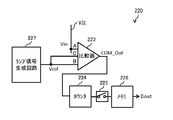
- the ADC 220 includes, for example, a single slope A / D converter.
- the single slope A / D converter includes, for example, a lamp signal generation circuit 221, a switch 222, a comparator 223, a counter 224, a switch 225, and a memory 226. Has been done.
- the lamp signal generation circuit 221 generates a plurality of lamp signals (signals having a lamp waveform) that are time-shifted.
- the lamp signal generation circuit 221 generates, for example, two lamp signals (signals having a lamp waveform) that are staggered in time.
- the lamp signal of one of the two time-shifted lamp signals is a lamp signal (ramp signal VrefH) having a relatively low slope as compared with the other lamp signal of the two time-shifted lamp signals. ..
- the other lamp signal of the two time-shifted lamp signals is a lamp signal (ramp signal VrefL) having a relatively high slope as compared with the lamp signal VrefL.
- the switch 222 When the lamp signal VrefL is output from the lamp signal generation circuit 221, the switch 222 connects the output terminal of the lamp signal generation circuit 221 and the input terminal of the lamp signal VrefL in the comparator 223 to each other.
- the switch 222 connects the output terminal of the lamp signal generation circuit 221 and the input terminal of the lamp signal VrefH in the comparator 223 to each other.
- the lamp signal generation circuit 221 may have two lamp signal generation circuits (LG lamp signal generation circuit 221A and HG lamp signal generation circuit 221B).
- the output terminal of the LG lamp signal generation circuit 221A may be connected to the input terminal B of the comparator 223, and the output terminal of the HG lamp signal generation circuit 221B may be connected to the input terminal C of the comparator 223.
- the LG lamp signal generation circuit 221A generates a lamp signal having a relatively low slope as compared with the HG lamp signal generation circuit 221B, based on the clock given by the system control circuit 24.
- the HG lamp signal generation circuit 221B generates a lamp signal having a relatively high slope as compared with the LG lamp signal generation circuit 221A, based on the clock given by the system control circuit 24.
- the LG lamp signal generation circuit 221A and the HG lamp signal generation circuit 221B may each include, for example, a DAC (digital-to-analog conversion circuit) that generates a lamp signal (a signal of a lamp waveform).
- the comparator 223 includes a signal voltage Vin of the data output line VSL corresponding to the signal output from each sensor pixel 11 in the nth column, and two signal generation circuits (LG lamp signal generation circuit 221A and HG lamp signal generation circuit 221B). ) And the lamp signals VrefH and VrefL of the lamp waveform are compared.
- the comparator 223 outputs, for example, when the lamp signal VrefH or the lamp signal VrefL is larger than the signal voltage Vin, the output becomes "H” level, and when the lamp signal VrefH or the lamp signal VrefL is equal to or less than the signal voltage Vin, the output becomes "H” level. It becomes “L” level.
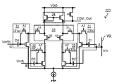
- the comparator 223 has a pipeline configuration in which an input capacitance, an operation amplification transistor, and an AZ switch are provided for the number of lamp signals input to the comparator 223 (for example, two systems). As shown in FIG. 5, for example, the comparator 223 has an operation amplifier circuit 31 (lamp side circuit 31a, pixel side circuit 31b) and an operation amplification circuit 32 (lamp side circuit 32a, pixel side circuit 32b). are doing.
- the operational amplifier circuit 31 (lamp side circuit 31a, pixel side circuit 31b) is an amplifier circuit that amplifies the difference between the pixel signal (signal voltage Vin) and the lamp signal VrefH of the HG lamp signal generation circuit 221B.
- the operational amplifier circuit 32 (ramp side circuit 32a, pixel side circuit 32b) is an amplifier circuit that amplifies the difference between the pixel signal (signal voltage Vin) and VrefL of the LG lamp signal generation circuit 221A.
- the lamp-side circuit 31a includes, for example, a capacitor C4 as an input capacitance, an operation amplification transistor, and an AZ switch.
- the pixel-side circuit 31b includes, for example, a capacitor C1 as an input capacitance, an operation amplification transistor, and an AZ switch.
- the lamp-side circuit 32a includes, for example, a capacitor C3 as an input capacitance, an operation amplification transistor, and an AZ switch.
- the pixel-side circuit 32b includes, for example, a capacitor C2 as an input capacitance, an operation amplification transistor, and an AZ switch.
- the comparator 223 further includes, for example, an output load circuit 34 and a connection circuit 33, as shown in FIG.
- the output load circuit 34 is a circuit that serves as an output load for the operation amplifier circuit 31 (lamp side circuit 31a, pixel side circuit 31b) and the operation amplification circuit 32 (lamp side circuit 32a, pixel side circuit 32b).
- the connection circuit 33 is a circuit that connects either the operation amplifier circuit 31 (lamp side circuit 31a, pixel side circuit 31b) or the operation amplification circuit 32 (lamp side circuit 32a, pixel side circuit 32b) to the output load circuit 34. be.
- the comparator 223 is provided with three input terminals A, B, and C.
- the input terminal A is an input terminal of the pixel side circuits 31b and 32b of the operation amplifier circuits 31 and 32, and is connected to the data output line VSL.
- the input terminal B is an input terminal of the lamp side circuit 32a of the operation amplifier circuit 32, and is connected to an output terminal of the lamp signal generation circuit 221 from which the lamp signal VrefL is output.
- the input terminal C is an input terminal of the lamp side circuit 31a of the operation amplifier circuit 31, and is connected to an output terminal of the lamp signal generation circuit 221 from which the lamp signal VrefH is output.
- the counter 224 is an asynchronous counter, and a clock is given from the system control circuit 24 under the control by a control signal given from the system control circuit 24, and a down (DOWN) count or an up (UP) count is given in synchronization with the clock.
- a clock is given from the system control circuit 24 under the control by a control signal given from the system control circuit 24, and a down (DOWN) count or an up (UP) count is given in synchronization with the clock.
- the analog signal supplied from each sensor pixel 11 via the data output line VSL for each column is converted into an N-bit digital signal by each operation of the comparator 223 and the counter 224 in the plurality of AD 220s. It is stored in the memory 226.
- FIG. 6 shows an example of various waveforms in the ADC 220.
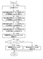
- FIG. 7 shows an example of a signal processing procedure in the solid-state image sensor 1.
- the solid-state image sensor 1 executes auto-zero (AZ) of the ADC 220 (step S101).
- the ADC 220 performs an auto-zero (AZ) operation in which the three input terminals A, B, and C of the comparator 223 have the same voltage under the control of the system control circuit 24.
- the ADC 220 applies the on-voltage of the transistor to the AZ, S0, and S1 under the control of the system control circuit 24, for example, so that the voltages applied to the three input terminals A, B, and C of the comparator 223 are equal to each other. , C1, C2, C3, C4 are charged.
- the solid-state image sensor 1 acquires the AD conversion value (D_high, D_low) of the pixel signal Vin at the time of the reset operation (P phase).
- the ADC 220 applies the on voltage of the transistor to S0 and the off voltage of the transistor to AZ and S1 under the control of the system control circuit 24 during the reset operation (reset period). Subsequently, the lamp signal generation circuit 221 inputs the P-phase lamp signal VrefH to the input terminal C of the comparator 223. At this time, the P-phase pixel signal Vin output from the pixel 11 during the reset operation is given to the data output line VSL. As a result, the comparator 223 acquires the P-phase lamp signal VrefH via the input terminal C, and acquires the P-phase pixel signal Vin via the input terminal A (step S102).
- the comparator 223 When the P-phase pixel signal Vin is smaller than the P-phase lamp signal VrefH, the comparator 223 outputs the Hi (High) comparison result signal COM_Out, and the P-phase pixel signal Vin is the P-phase lamp signal VrefH. When it is larger than, the comparison result signal COM_Out of Lo (Low) is output. The comparator 223 outputs the comparison result signal COM_Out to the counter 224. The counter 224 counts up the internal counter only while the Hi comparison result signal COM_Out is supplied, based on the clock signal supplied from the system control circuit 24. The count result is the P-phase AD conversion value D_high. The switch 225 is turned on when the counting operation is completed, and stores the P-phase AD conversion value D_high in the memory 226. In this way, the ADC 220 acquires the AD conversion value D_high of the P phase (step S102).
- the ADC 220 applies the on voltage of the transistor to S1 and the off voltage of the transistor to AZ and S0 under the control of the system control circuit 24 during the reset operation (reset period).
- the lamp signal generation circuit 221 inputs the P-phase lamp signal VrefL to the input terminal B of the comparator 223.
- the P-phase pixel signal Vin output from the pixel 11 during the reset operation is given to the data output line VSL.
- the comparator 223 acquires the P-phase lamp signal VrefL via the input terminal B, and acquires the P-phase pixel signal Vin via the input terminal A (step S103).
- the comparator 223 When the P-phase pixel signal Vin is smaller than the P-phase lamp signal VrefL, the comparator 223 outputs the Hi (High) comparison result signal COM_Out, and the P-phase pixel signal Vin is the P-phase lamp signal VrefL. When it is larger than, the comparison result signal COM_Out of Lo (Low) is output. The comparator 223 outputs the comparison result signal COM_Out to the counter 224. The counter 224 counts up the internal counter only while the Hi comparison result signal COM_Out is supplied, based on the clock signal supplied from the system control circuit 24. The count result is the P-phase AD conversion value D_low. The switch 225 is turned on when the counting operation is completed, and stores the P-phase AD conversion value D_low in the memory 226. In this way, the ADC 220 acquires the AD conversion value D_low of the P phase (step S103).
- the solid-state image sensor 1 acquires the AD conversion value (D_high, D_low) of the pixel signal Vin at the time of signal output (D phase).
- the ADC 220 applies the on voltage of the transistor to S0 and the off voltage of the transistor to AZ and S1 under the control of the system control circuit 24 at the time of signal output (signal output period).
- the lamp signal generation circuit 221 inputs the D-phase lamp signal VrefH to the input terminal C of the comparator 223.
- the D-phase pixel signal Vin output from the pixel 11 at the time of signal output is given to the data output line VSL.
- the comparator 223 acquires the D-phase lamp signal VrefH via the input terminal C, and acquires the D-phase pixel signal Vin via the input terminal A (step S104).
- the comparator 223 outputs the Hi (High) comparison result signal COM_Out when the D-phase pixel signal Vin is smaller than the D-phase lamp signal VrefH, and the D-phase pixel signal Vin is the D-phase lamp signal VrefH.
- the comparison result signal COM_Out of Lo (Low) is output.
- the comparator 223 outputs the comparison result signal COM_Out to the counter 224.
- the counter 224 counts up the internal counter only while the Hi comparison result signal COM_Out is supplied, based on the clock signal supplied from the system control circuit 24.
- the count result is the AD conversion value D_high of the D phase.
- the switch 225 is turned on when the counting operation is completed, and stores the AD conversion value D_high of the D phase in the memory 226. In this way, the ADC 220 acquires the AD conversion value D_high of the D phase (step S104).
- the ADC 220 applies the on voltage of the transistor to S1 and the off voltage of the transistor to AZ and S0 under the control of the system control circuit 24 at the time of signal output (signal output period).
- the lamp signal generation circuit 221 inputs the D-phase lamp signal VrefL to the input terminal B of the comparator 223.
- the D-phase pixel signal Vin output from the pixel 11 at the time of signal output is given to the data output line VSL.
- the comparator 223 acquires the D-phase lamp signal VrefL via the input terminal B, and acquires the D-phase pixel signal Vin via the input terminal A (step S105).
- the comparator 223 outputs a Hi (High) comparison result signal COM_Out when the D-phase pixel signal Vin is smaller than the D-phase lamp signal VrefL, and the D-phase pixel signal Vin is the D-phase lamp signal VrefL. When it is larger than, the comparison result signal COM_Out of Lo (Low) is output.
- the comparator 223 outputs the comparison result signal COM_Out to the counter 224.
- the counter 224 counts up the internal counter only while the Hi comparison result signal COM_Out is supplied, based on the clock signal supplied from the system control circuit 24.
- the count result is the AD conversion value D_low of the D phase.
- the switch 225 is turned on when the counting operation is completed, and stores the AD conversion value D_low of the D phase in the memory 226. In this way, the ADC 220 acquires the AD conversion value D_low of the D phase (step S105).
- the ADC 220 acquires the difference between the AD conversion value D_high of the D phase and the AD conversion value D_high of the P phase, and stores the acquired difference as a gradation signal Dout_high in the memory 226. Further, the ADC 220 acquires the difference between the AD conversion value D_low of the D phase and the AD conversion value D_low of the P phase, and stores the acquired difference as the gradation signal Dout_low in the memory 226. In this way, the ADC 220 acquires the gradation signals Dout_high and Dout_low (step S106).
- the AD conversion circuit 22 reads the gradation signals Dout_high and Dout_low from the memory 307 of each ADC 220 under the control of the horizontal drive circuit 23, and outputs them to the output circuit 25 via the horizontal output line.
- the output circuit 25 determines whether or not the gradation signal Dout_high is larger than the threshold value Dth (step S107). As a result, when the gradation signal Dout_high is larger than the threshold value Dth (step S107; Y), the output circuit 25 selects the gradation signal Dout_low of the pixel sequence corresponding to the gradation signal Dout_high larger than the threshold value Dth. , Output (step S108). On the other hand, when the gradation signal Dout_high is equal to or less than the threshold value Dth (step S107; N), the output circuit 25 selects and outputs the gradation signal Dout_high equal to or less than the threshold value Dth (step S109). In this way, the AD conversion in the solid-state image sensor 1 is performed.
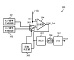
- the ADC 300 includes, for example, two lamp signal generation circuits 301 and 302, a switch 303, a comparator 304, a counter 305, a switch 306, a memory 307, and an illuminance determination unit 308.
- the two lamp signal generation circuits 301 and 302 are circuits that generate two lamp signals having different slopes from each other.
- the output terminal of one lamp signal generation circuit 301 is connected to one input terminal of the switch 303, and the output terminal of the other lamp signal generation circuit 302 is connected to the other input terminal of the switch 303.
- One input terminal D of the comparator 304 is connected to the data output line VSL, and the other input terminal E of the comparator 304 is connected to the output terminal of the switch 303.
- the comparator 304 outputs a comparison result (COM_Out) between the pixel signal Vin input to the input terminal D and the lamp signal input to the input terminal E.
- the illuminance determination unit 308 outputs a selection signal for selecting one of the two lamp signal generation circuits 301 and 302 to the switch 303 based on the comparison result (COM_Out).
- the lamp signal selected by the selection signal from the illuminance determination unit 308 is input to the input terminal E of the comparator 304.
- the magnitude (COM_Out) of each pixel signal is independently detected, and the analog gain is set for each pixel signal according to the detection result.
- the analog gain is set by feeding back the detection result, there is a problem that a delay occurs before the detection result is reflected.
- temporal serial processing is performed for comparison between the pixel signal according to the amount of incident light and the two time-shifted lamp signals VrefH and VrefL, which are obtained by the above comparison.
- An image signal according to the result is generated.
- the gradation signal D_high and the gradation signal D_high are based on the magnitude relationship between the gradation signal D_high generated by using the lamp signal VrefH and the predetermined threshold value Dth. It is possible to determine which of the tonal signals D_low is used to generate the image signal.
- two lamp signal generation circuits 221A and 221B are provided. This makes it possible for the lamp signal generation circuit 221A on one side and the lamp signal generation circuit 221B on the other side to shift the lamp signals in time or to make the slopes different from each other. As a result, for example, either the gradation signal D_high generated by using one lamp signal generation circuit 221B or the gradation signal D_low generated by using the other lamp signal generation circuit 221A is used for image signal generation. You can decide whether or not to do it. As described above, in the present embodiment, since it is possible to select an appropriate analog gain signal in the processing after the comparator 223, it is not necessary to provide a feedback circuit. As a result, it is possible to suppress the occurrence of a delay as in the case of providing a circuit for feeding back the detection result.
- the operational amplifier circuit 31 for the pixel signal Vin and the lamp signal VrefH the operational amplifier circuit 32 for the pixel signal Vin and the lamp signal VrefL, and the operational amplifier circuits 31, 32.
- a connection circuit 33 is provided to connect either of them with the output load circuit 34 that adds the output of the operation amplifier circuits 31 and 32.
- the serial processing for example, the gradation signal D_high and the gradation based on the magnitude relationship between the gradation signal D_high generated by using the lamp signal VrefH and the predetermined threshold value Dth. It is possible to determine which of the signals D_low is used to generate the image signal. As described above, in the present embodiment, since it is possible to select an appropriate analog gain signal in the processing after the comparator 223, it is not necessary to provide a feedback circuit. As a result, it is possible to suppress the occurrence of a delay as in the case of providing a circuit for feeding back the detection result.
- the present embodiment it is determined whether to use the gradation signal Dout_high or the gradation signal Dout_low for generating the image signal based on the magnitude relationship between the gradation signal Dout_high and the predetermined threshold value Dth. Will be done.
- the present embodiment since it is possible to select an appropriate analog gain signal in the processing after the comparator 223, it is not necessary to provide a feedback circuit. As a result, it is possible to suppress the occurrence of a delay as in the case of providing a circuit for feeding back the detection result.
- FIG. 10 shows an example of the circuit configuration of the comparator 223 in the solid-state image sensor 1 according to this modification.
- the comparator 223 has two input circuits 35 and 36 having different input capacitances from each other.
- One input circuit 35 is provided at the input terminal B, and the other input circuit 36 is provided at the input terminal C.
- the input circuit 35 includes, for example, a capacitor C3 connected in series to the input terminal B and a capacitor C5 having one end connected to a terminal opposite to the input terminal B.
- the input circuit 36 includes, for example, a capacitor C4 connected in series with the input terminal C.
- the comparator 223 can perform temporal serial processing for comparison between the pixel signal Vin and the plurality of lamp signals shifted in time. Therefore, the same effect as that of the above embodiment can be obtained without providing a plurality of lamp signal generation circuits.
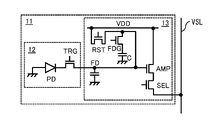
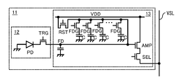
- the reading circuit 13 of the sensor pixel 11 may have a switching circuit for switching the conversion efficiency of photoelectric conversion.
- the switching circuit includes, for example, as shown in FIG. 11, a reset transistor FDG provided between the source / drain terminal of the reset transistor TST and the gate terminal of the amplification transistor AMP, and a reset transistor FDG at one end. It is configured to include a capacitor C connected to a source / drain terminal on the transistor TST side.
- FIG. 12 shows an example of the circuit configuration of the comparator 223 in the solid-state image sensor 1 according to this modification.
- the two input terminals B and C of the comparator 223 are connected to each other via wiring.
- AZ0 is an AZ signal for one system in the pipeline configuration.
- AZ1 is an AZ signal for the other system in the pipeline configuration.
- the lamp-side circuit 31a includes, for example, a capacitor C4 as an input capacitance, an operation amplification transistor, and an AZ1 switch.
- the pixel-side circuit 31b includes, for example, a capacitor C1 as an input capacitance, an operation amplification transistor, and an AZ1 switch.
- the lamp-side circuit 32a includes, for example, a capacitor C3 as an input capacitance, an operation amplification transistor, and an AZ0 switch.
- the pixel-side circuit 32b includes, for example, a capacitor C2 as an input capacitance, an operation amplification transistor, and an AZ0 switch.
- FIG. 13 shows an example of various waveforms in the solid-state image sensor 1.
- FIG. 14 shows an example of a signal processing procedure in the solid-state image sensor 1.
- the solid-state image sensor 1 executes auto-zero (AZ) of AZ0 in the ADC 220 (step S201).
- the ADC 220 performs an auto-zero (AZ) operation in which the two input terminals A and B of the comparator 223 have the same voltage under the control of the system control circuit 24.
- the ADC 220 applies a transistor on voltage to AZ0, S0, S1 under control by, for example, the system control circuit 24, and a capacitor so that the voltages applied to the two input terminals A and B of the comparator 223 are equal to each other. Charge C2 and C3.
- the solid-state image sensor 1 acquires the AD conversion value (D_low) of the pixel signal Vin during the reset operation (P phase).
- the ADC 220 applies the on voltage of the transistor to S0 and the off voltage of the transistor to AZ0, AZ1, S1 under the control of the system control circuit 24.
- the lamp signal generation circuit 227 inputs the P-phase lamp signal Vref to the input terminal B of the comparator 223.
- the conversion efficiency is switched by turning on the conversion transistor FDG, and the data output line VSL is given a P-phase pixel signal Vin'according to the conversion efficiency (low conversion efficiency) after switching.
- the comparator 223 acquires the P-phase lamp signal Vref via the input terminal B, and acquires the P-phase pixel signal Vin'via the input terminal A (step S202).
- the comparator 223 When the P-phase pixel signal Vin'is smaller than the P-phase lamp signal Vref, the comparator 223 outputs a Hi (High) comparison result signal COM_Out, and the P-phase pixel signal Vin'is a P-phase lamp. When it is larger than the signal Vref, the comparison result signal COM_Out of Lo (Low) is output. The comparator 223 outputs the comparison result signal COM_Out to the counter 224. The counter 224 counts up the internal counter only while the Hi comparison result signal COM_Out is supplied, based on the clock signal supplied from the system control circuit 24. The count result is the P-phase AD conversion value D_low. The switch 225 is turned on when the counting operation is completed, and stores the P-phase AD conversion value D_low in the memory 226. In this way, the ADC 220 acquires the AD conversion value D_low of the P phase (step S202).
- the solid-state image sensor 1 executes auto-zero (AZ) of AZ1 in the ADC 220 (step S203).
- the ADC 220 performs an auto-zero (AZ) operation in which the two input terminals A and C of the comparator 223 have the same voltage under the control of the system control circuit 24.
- the ADC 220 applies the on-voltage of the transistor to the AZ1 and S1 under the control of, for example, the system control circuit 24, and the capacitors C1 and C1 so that the voltages applied to the two input terminals A and C of the comparator 223 are equal to each other.
- Charge C4 Charge C4.
- the ADC 220 applies the on voltage of the transistor to S1 and the off voltage of the transistor to AZ0, AZ1, S0 under the control of the system control circuit 24.
- the lamp signal generation circuit 227 inputs the P-phase lamp signal Vref to the input terminal C of the comparator 223.
- the comparator 223 acquires the P-phase lamp signal Vref via the input terminal C, and acquires the P-phase pixel signal Vin via the input terminal A (step S204).
- the comparator 223 When the P-phase pixel signal Vin is smaller than the P-phase lamp signal Vref, the comparator 223 outputs the Hi (High) comparison result signal COM_Out, and the P-phase pixel signal Vin is the P-phase lamp signal Vref. When it is larger than, the comparison result signal COM_Out of Lo (Low) is output. The comparator 223 outputs the comparison result signal COM_Out to the counter 224. The counter 224 counts up the internal counter only while the Hi comparison result signal COM_Out is supplied, based on the clock signal supplied from the system control circuit 24. The count result is the P-phase AD conversion value D_high. The switch 225 is turned on when the counting operation is completed, and stores the P-phase AD conversion value D_high in the memory 226. In this way, the ADC 220 acquires the AD conversion value D_high of the P phase (step S204).
- the solid-state image sensor 1 acquires the AD conversion value (D_high, D_low) of the pixel signal Vin at the time of signal output (D phase).
- the ADC 220 applies the on voltage of the transistor to S1 and the off voltage of the transistor to AZ0, AZ1, S0 under the control of the system control circuit 24 at the time of signal output (signal output period). .. Subsequently, the lamp signal generation circuit 227 inputs the D-phase lamp signal Vref to the input terminal C of the comparator 223. At this time, since the conversion transistor FDG is turned off, the conversion efficiency has returned to the original state, and the data output line VSL is given a P-phase pixel signal Vin corresponding to the conversion efficiency in the original state. ..
- the comparator 223 acquires the D-phase lamp signal Vref via the input terminal C, and acquires the D-phase pixel signal Vin via the input terminal A (step S205).
- the comparator 223 outputs the Hi (High) comparison result signal COM_Out when the D-phase pixel signal Vin is smaller than the D-phase lamp signal Vref, and the D-phase pixel signal Vin is the D-phase lamp signal Vref.
- the comparison result signal COM_Out of Lo (Low) is output.
- the comparator 223 outputs the comparison result signal COM_Out to the counter 224.
- the counter 224 counts up the internal counter only while the Hi comparison result signal COM_Out is supplied, based on the clock signal supplied from the system control circuit 24.
- the count result is the AD conversion value D_high of the D phase.
- the switch 225 is turned on when the counting operation is completed, and stores the AD conversion value D_high of the D phase in the memory 226. In this way, the ADC 220 acquires the AD conversion value D_high of the D phase (step S205).
- the ADC 220 applies the on voltage of the transistor to S0 and the off voltage of the transistor to AZ0, AZ1, S1 under the control of the system control circuit 24 at the time of signal output (signal output period).
- the lamp signal generation circuit 227 inputs the D-phase lamp signal Vref to the input terminal B of the comparator 223.
- the conversion efficiency is switched by turning on the conversion transistor FDG, and the data output line VSL is given a P-phase pixel signal Vin'according to the conversion efficiency (low conversion efficiency) after switching.
- the comparator 223 acquires the D-phase lamp signal Vref via the input terminal B, and acquires the D-phase pixel signal Vin via the input terminal A (step S206).
- the comparator 223 outputs the Hi (High) comparison result signal COM_Out when the D-phase pixel signal Vin is smaller than the D-phase lamp signal Vref, and the D-phase pixel signal Vin is the D-phase lamp signal Vref. When it is larger than, the comparison result signal COM_Out of Lo (Low) is output.
- the comparator 223 outputs the comparison result signal COM_Out to the counter 224.
- the counter 224 counts up the internal counter only while the Hi comparison result signal COM_Out is supplied, based on the clock signal supplied from the system control circuit 24.
- the count result is the AD conversion value D_low of the D phase.
- the switch 225 is turned on when the counting operation is completed, and stores the AD conversion value D_low of the D phase in the memory 226. In this way, the ADC 220 acquires the AD conversion value D_low of the D phase (step S206).
- the ADC 220 acquires the difference between the AD conversion value D_high of the D phase and the AD conversion value D_high of the P phase, and stores the acquired difference as a gradation signal Dout_high in the memory 226. Further, the ADC 220 acquires the difference between the AD conversion value D_low of the D phase and the AD conversion value D_low of the P phase, and stores the acquired difference as the gradation signal Dout_low in the memory 226. In this way, the ADC 220 acquires the gradation signals Dout_high and Dout_low (step S207).
- the AD conversion circuit 22 reads the gradation signals Dout_high and Dout_low from the memory 307 of each ADC 220 under the control of the horizontal drive circuit 23, and outputs them to the output circuit 25 via the horizontal output line.
- the output circuit 25 determines whether or not the gradation signal Dout_high is larger than the threshold value Dth (step S208). As a result, when the gradation signal Dout_high is larger than the threshold value Dth (step S208; Y), the output circuit 25 selects the detection signal Dout_low of the pixel sequence corresponding to the gradation signal Dout_high larger than the threshold value Dth. Output (step S209). On the other hand, when the detection signal Dout_high is equal to or less than the threshold value Dth (step S208; N), the output circuit 25 selects and outputs the gradation signal Dout_high equal to or less than the threshold value Dth (step S210). In this way, the AD conversion in the solid-state image sensor 1 is performed.
- the sensor pixel 11 is provided with a switching circuit for switching the conversion efficiency of photoelectric conversion.
- the P phase is based on the P phase pixel signal Vin'according to the conversion efficiency (low conversion efficiency) after switching and the P phase lamp signal Vref.
- AD conversion value D_low is obtained
- P-phase AD conversion value D_high is obtained based on the P-phase pixel signal Vin corresponding to the conversion efficiency (high conversion efficiency) before switching and the P-phase lamp signal Vref. ..
- the D-phase AD conversion value D_high is obtained based on the P-phase pixel signal Vin corresponding to the conversion efficiency (high conversion efficiency) before switching and the D-phase lamp signal Vref, and the conversion efficiency after switching (high conversion efficiency).
- the AD conversion value D_low of the D phase is obtained based on the pixel signal Vin'of the D phase corresponding to the low conversion efficiency) and the lamp signal Vref of the D phase.
- the gradation signal Dout_high is obtained from the difference between the AD conversion value D_high of the D phase and the AD conversion value D_high of the P phase, and the AD conversion value D_low of the D phase and the AD of the P phase are obtained.
- the gradation signal Dout_low is obtained from the difference from the conversion value D_low. After that, for example, it is determined whether to use the gradation signal D_high or the gradation signal D_low for generating the image signal based on the magnitude relationship between the gradation signal Dout_high and the predetermined threshold value Dth.
- D_low the gradation signal
- D_low the gradation signal
- the conversion transistor FDG when the operation amplifier circuit 32 and the output load circuit 34 are connected via the connection circuit 33, the conversion transistor FDG is turned on, and the operation amplifier circuit 31 and the output are output via the connection circuit 33. When the load circuit 34 is connected, the conversion transistor FDG is turned off. In this way, by synchronizing the switching of the pipeline in the comparator 223 and the switching of the conversion efficiency of the photoelectric conversion in the sensor pixel 11, the pixel signals Vin, Vin'and the plurality of lamp signals Vref that are time-shifted are It is possible to perform temporal serial processing for comparison with. Therefore, the same effect as that of the above embodiment can be obtained without providing a plurality of lamp signal generation circuits.
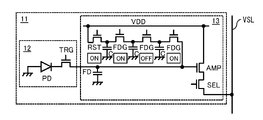
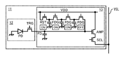
- the switching circuit may have a plurality of switching tragista FDGs connected in series and controlled independently of each other, for example, as shown in FIGS. 15 and 16.
- a capacitor C may be provided at one end, which is connected to the source / drain terminals of two switching tradista FDGs adjacent to each other.
- the system control circuit 24 applies a pulse independently to the gate of each switching tradista FDG to turn on / off a plurality of switching tradista FDGs (and thus to switch the conversion efficiency of photoelectric conversion). conduct.
- the system control circuit 24 turns on all three switching tradistas FDG, for example, as shown in FIG. As a result, the three capacitors C are connected in parallel to the floating diffusion FD, so that the conversion efficiency of photoelectric conversion decreases according to the number of connected capacitors C.
- the system control circuit 24 turns on only two switching transistors FDG on the amplification transistor AMP side among the three switching transistor FDGs. As a result, the two capacitors C are connected in parallel to the floating diffusion FD, so that the conversion efficiency of photoelectric conversion decreases according to the number of connected capacitors C.
- the system control circuit 24 turns on only the two switching transistors FDG at both ends of the three switching transistor FDGs, for example, as shown in FIG. As a result, one capacitor C on the AMP side of the amplification transistor is connected in parallel to the floating diffusion FD, so that the conversion efficiency of photoelectric conversion decreases according to the number of connected capacitors C. For example, as shown in FIG. 20, the system control circuit 24 turns on only two switching transistors FDG on the reset transistor RST side among the three switching transistor FDGs. At this time, since the capacitor C is not connected to the floating diffusion FD, the conversion efficiency of photoelectric conversion is not particularly different from that before switching.
- the switching circuit is a switching transistor FDG in which one end (source / drain terminal) is connected to the source / drain terminal of the reset transistor RST and the gate terminal of the amplification transistor AMP. May have. At this time, the capacitor C may be connected to the other end (source / drain terminal) of the switching transistor FDG.
- the system control circuit 24 turns on the switching transistor FDG, so that the capacitor C is connected in parallel to the floating diffusion FD via the switching transistor FDG. As a result, the conversion efficiency of photoelectric conversion decreases according to the number of connected capacitors C.
- the switching circuit may have a plurality of switching tragista FDGs connected in parallel to each other and controlled independently of each other, for example, as shown in FIGS. 22 and 23.
- a capacitor C may be provided at one end, which is connected to the source / drain terminals of two switching tradista FDGs adjacent to each other.
- the system control circuit 24 applies a pulse independently to the gate of each switching tradista FDG to turn on / off a plurality of switching tradista FDGs (and thus to switch the conversion efficiency of photoelectric conversion). conduct.
- the system control circuit 24 turns on all three switching tradistas FDG, for example, as shown in FIG. As a result, the three capacitors C are connected in parallel to the floating diffusion FD, so that the conversion efficiency of photoelectric conversion decreases according to the number of connected capacitors C.
- the system control circuit 24 turns on only two switching transistors FDG on the amplification transistor AMP side among the three switching transistor FDGs. As a result, the two capacitors C are connected in parallel to the floating diffusion FD, so that the conversion efficiency of photoelectric conversion decreases according to the number of connected capacitors C.
- the system control circuit 24 turns on only one switching transistor FDG on the amplification transistor AMP side among the three switching transistor FDGs.
- one capacitor C on the AMP side of the amplification transistor is connected in parallel to the floating diffusion FD, so that the conversion efficiency of photoelectric conversion decreases according to the number of connected capacitors C.
- the system control circuit 24 turns off all three switching tradistas FDG, for example, as shown in FIG. At this time, since the capacitor C is not connected to the floating diffusion FD, the conversion efficiency of photoelectric conversion is not particularly different from that before switching.
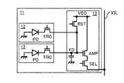
- a plurality of pixel circuits 12 may share one readout circuit 13.
- the two pixel circuits 12 may share one readout circuit 13.
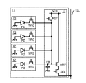
- the four pixel circuits 12 may share one read circuit 13.
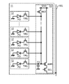
- a large number of pixel circuits 12 may share one read circuit 13.
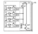
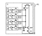
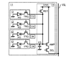
- the vertical drive circuit 21 turns on the transfer transistor TRG included in one of the four pixel circuits 12 as shown in FIG. 31, for example. As a result, the electric charge from one pixel circuit 12 is transferred to the floating diffusion FD. Further, the vertical drive circuit 21 turns on the transfer transistor TRG included in two of the four pixel circuits 12 as shown in FIG. 32, for example. As a result, the electric charge from the two pixel circuits 12 is transferred to the floating diffusion FD, so that the electric charge accumulated in the floating diffusion FD is compared with the case where the electric charge from the one pixel circuit 12 is transferred to the floating diffusion FD. You can increase the amount. As a result, the signal gain can be increased by the amount of increase in the amount of electric charge.
- the vertical drive circuit 21 turns on the transfer transistor TRG included in three pixel circuits 12 out of the four pixel circuits 12, for example, as shown in FIG. 33.
- the electric charge from the three pixel circuits 12 is transferred to the floating diffusion FD, so that the electric charge accumulated in the floating diffusion FD is compared with the case where the electric charge from the two pixel circuits 12 is transferred to the floating diffusion FD.
- the signal gain can be increased by the amount of increase in the amount of electric charge.
- the vertical drive circuit 21 turns on the transfer transistor TRG included in all four pixel circuits 12, for example, as shown in FIG. 34.
- the electric charge from the four pixel circuits 12 is transferred to the floating diffusion FD, so that the electric charge accumulated in the floating diffusion FD is compared with the case where the electric charge from the three pixel circuits 12 is transferred to the floating diffusion FD.
- the signal gain can be increased by the amount of increase in the amount of electric charge.
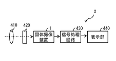
- FIG. 35 shows an example of a schematic configuration of an image pickup system 2 provided with a solid-state image pickup device 1 according to the above embodiment and a modified example thereof.
- the image pickup system 2 includes, for example, an optical system 410, a shutter mechanism 420, a solid-state image pickup device 1, a signal processing circuit 430, and a display unit 440.
- the optical system 410 forms an image of image light (incident light) from the subject on the image pickup surface of the solid-state image pickup device 1.
- the shutter mechanism 420 controls the light irradiation period and the light shielding period to the solid-state image sensor 1 by opening and closing.
- the solid-state imaging device 1 receives the image light (incident light) incident from the optical system 410, and outputs the image data corresponding to the received image light (incident light) to the signal processing circuit 430.
- the signal processing circuit 430 processes the image data input from the solid-state image sensor 1 to generate video data.
- the signal processing circuit 430 further generates a video signal corresponding to the generated video data and outputs the video signal to the display unit 440.
- the display unit 440 displays an image based on the image signal input from the signal processing circuit 230.
- the solid-state image pickup device 1 according to the above embodiment and its modification is applied to the image pickup system 2. This makes it possible to provide a system using highly dynamic captured images.
- the technique according to the present disclosure can be applied to various products.
- the technology according to the present disclosure is realized as a device mounted on a moving body of any kind such as an automobile, an electric vehicle, a hybrid electric vehicle, a motorcycle, a bicycle, a personal mobility, an airplane, a drone, a ship, and a robot. You may.
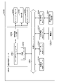
- FIG. 36 is a block diagram showing a schematic configuration example of a vehicle control system, which is an example of a mobile control system to which the technique according to the present disclosure can be applied.
- the vehicle control system 12000 includes a plurality of electronic control units connected via the communication network 12001.
- the vehicle control system 12000 includes a drive system control unit 12010, a body system control unit 12020, an outside information detection unit 12030, an in-vehicle information detection unit 12040, and an integrated control unit 12050.
- a microcomputer 12051, an audio image output unit 12052, and an in-vehicle network I / F (interface) 12053 are shown as a functional configuration of the integrated control unit 12050.
- the drive system control unit 12010 controls the operation of the device related to the drive system of the vehicle according to various programs.
- the drive system control unit 12010 has a driving force generator for generating a driving force of a vehicle such as an internal combustion engine or a driving motor, a driving force transmission mechanism for transmitting the driving force to the wheels, and a steering angle of the vehicle. It functions as a control device such as a steering mechanism for adjusting and a braking device for generating braking force of the vehicle.
- the body system control unit 12020 controls the operation of various devices mounted on the vehicle body according to various programs.
- the body system control unit 12020 functions as a keyless entry system, a smart key system, a power window device, or a control device for various lamps such as headlamps, back lamps, brake lamps, turn signals or fog lamps.
- the body system control unit 12020 may be input with radio waves transmitted from a portable device that substitutes for the key or signals of various switches.
- the body system control unit 12020 receives inputs of these radio waves or signals and controls a vehicle door lock device, a power window device, a lamp, and the like.
- the vehicle outside information detection unit 12030 detects information outside the vehicle equipped with the vehicle control system 12000.
- the image pickup unit 12031 is connected to the vehicle outside information detection unit 12030.
- the vehicle outside information detection unit 12030 causes the image pickup unit 12031 to capture an image of the outside of the vehicle and receives the captured image.
- the vehicle outside information detection unit 12030 may perform object detection processing or distance detection processing such as a person, a vehicle, an obstacle, a sign, or a character on the road surface based on the received image.
- the image pickup unit 12031 is an optical sensor that receives light and outputs an electric signal according to the amount of the light received.
- the image pickup unit 12031 can output an electric signal as an image or can output it as distance measurement information. Further, the light received by the image pickup unit 12031 may be visible light or invisible light such as infrared light.
- the in-vehicle information detection unit 12040 detects the in-vehicle information.
- a driver state detection unit 12041 that detects a driver's state is connected to the vehicle interior information detection unit 12040.
- the driver state detection unit 12041 includes, for example, a camera that images the driver, and the in-vehicle information detection unit 12040 determines the degree of fatigue or concentration of the driver based on the detection information input from the driver state detection unit 12041. It may be calculated, or it may be determined whether or not the driver has fallen asleep.
- the microcomputer 12051 calculates the control target value of the driving force generator, the steering mechanism, or the braking device based on the information inside and outside the vehicle acquired by the vehicle exterior information detection unit 12030 or the vehicle interior information detection unit 12040, and the drive system control unit.
- a control command can be output to 12010.
- the microcomputer 12051 realizes ADAS (Advanced Driver Assistance System) functions including vehicle collision avoidance or impact mitigation, follow-up driving based on inter-vehicle distance, vehicle speed maintenance driving, vehicle collision warning, vehicle lane deviation warning, and the like. It is possible to perform cooperative control for the purpose of.
- ADAS Advanced Driver Assistance System
- the microcomputer 12051 controls the driving force generating device, the steering mechanism, the braking device, and the like based on the information around the vehicle acquired by the vehicle exterior information detection unit 12030 or the vehicle interior information detection unit 12040. It is possible to perform coordinated control for the purpose of automatic driving that runs autonomously without depending on the operation.
- the microcomputer 12051 can output a control command to the body system control unit 12020 based on the information outside the vehicle acquired by the vehicle outside information detection unit 12030.
- the microcomputer 12051 controls the headlamps according to the position of the preceding vehicle or the oncoming vehicle detected by the outside information detection unit 12030, and performs cooperative control for the purpose of anti-glare such as switching the high beam to the low beam. It can be carried out.
- the audio image output unit 12052 transmits an output signal of at least one of audio and image to an output device capable of visually or audibly notifying information to the passenger or the outside of the vehicle.
- an audio speaker 12061, a display unit 12062, and an instrument panel 12063 are exemplified as output devices.
- the display unit 12062 may include, for example, at least one of an onboard display and a head-up display.
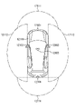
- FIG. 37 is a diagram showing an example of the installation position of the image pickup unit 12031.
- the vehicle 12100 has image pickup units 12101, 12102, 12103, 12104, 12105 as image pickup units 12031.
- the image pickup units 12101, 12102, 12103, 12104, 12105 are provided, for example, at positions such as the front nose, side mirrors, rear bumpers, back doors, and the upper part of the windshield in the vehicle interior of the vehicle 12100.
- the image pickup unit 12101 provided in the front nose and the image pickup section 12105 provided in the upper part of the windshield in the vehicle interior mainly acquire an image in front of the vehicle 12100.
- the image pickup units 12102 and 12103 provided in the side mirror mainly acquire images of the side of the vehicle 12100.
- the image pickup unit 12104 provided in the rear bumper or the back door mainly acquires an image of the rear of the vehicle 12100.
- the images in front acquired by the image pickup units 12101 and 12105 are mainly used for detecting a preceding vehicle, a pedestrian, an obstacle, a traffic light, a traffic sign, a lane, or the like.
- FIG. 37 shows an example of the shooting range of the imaging units 12101 to 12104.
- the imaging range 12111 indicates the imaging range of the imaging unit 12101 provided on the front nose
- the imaging ranges 12112 and 12113 indicate the imaging range of the imaging units 12102 and 12103 provided on the side mirrors, respectively
- the imaging range 12114 indicates the imaging range.
- the imaging range of the imaging unit 12104 provided on the rear bumper or the back door is shown. For example, by superimposing the image data captured by the image pickup units 12101 to 12104, a bird's-eye view image of the vehicle 12100 can be obtained.
- At least one of the image pickup units 12101 to 12104 may have a function of acquiring distance information.
- at least one of the image pickup units 12101 to 12104 may be a stereo camera including a plurality of image pickup elements, or may be an image pickup element having pixels for phase difference detection.
- the microcomputer 12051 has a distance to each three-dimensional object within the image pickup range 12111 to 12114 based on the distance information obtained from the image pickup unit 12101 to 12104, and a temporal change of this distance (relative speed with respect to the vehicle 12100). By obtaining can. Further, the microcomputer 12051 can set an inter-vehicle distance to be secured in advance in front of the preceding vehicle, and can perform automatic braking control (including follow-up stop control), automatic acceleration control (including follow-up start control), and the like. In this way, it is possible to perform coordinated control for the purpose of automatic driving or the like that autonomously travels without relying on the driver's operation.
- automatic braking control including follow-up stop control
- automatic acceleration control including follow-up start control
- the microcomputer 12051 converts three-dimensional object data related to a three-dimensional object into two-wheeled vehicles, ordinary vehicles, large vehicles, pedestrians, electric poles, and other three-dimensional objects based on the distance information obtained from the image pickup units 12101 to 12104. It can be classified and extracted and used for automatic avoidance of obstacles. For example, the microcomputer 12051 distinguishes obstacles around the vehicle 12100 into obstacles that are visible to the driver of the vehicle 12100 and obstacles that are difficult to see. Then, the microcomputer 12051 determines the collision risk indicating the risk of collision with each obstacle, and when the collision risk is equal to or higher than the set value and there is a possibility of collision, the microcomputer 12051 via the audio speaker 12061 or the display unit 12062. By outputting an alarm to the driver and performing forced deceleration and avoidance steering via the drive system control unit 12010, driving support for collision avoidance can be provided.
- At least one of the image pickup units 12101 to 12104 may be an infrared camera that detects infrared rays.
- the microcomputer 12051 can recognize a pedestrian by determining whether or not a pedestrian is present in the captured image of the imaging unit 12101 to 12104.
- pedestrian recognition is, for example, a procedure for extracting feature points in an image captured by an image pickup unit 12101 to 12104 as an infrared camera, and pattern matching processing is performed on a series of feature points indicating the outline of an object to determine whether or not the pedestrian is a pedestrian. It is done by the procedure to determine.
- the audio image output unit 12052 determines the square contour line for emphasizing the recognized pedestrian.
- the display unit 12062 is controlled so as to superimpose and display. Further, the audio image output unit 12052 may control the display unit 12062 so as to display an icon or the like indicating a pedestrian at a desired position.
- the above is an example of a mobile control system to which the technique according to the present disclosure can be applied.
- the technique according to the present disclosure can be applied to the image pickup unit 12031 among the configurations described above.
- the solid-state image sensor 1 according to the above embodiment and its modification can be applied to the image pickup unit 12031.
- FIG. 38 is a diagram showing an example of a schematic configuration of an endoscopic surgery system to which the technique according to the present disclosure (the present technique) can be applied.
- FIG. 38 illustrates how the surgeon (doctor) 11131 is performing surgery on patient 11132 on patient bed 11133 using the endoscopic surgery system 11000.
- the endoscopic surgery system 11000 includes an endoscope 11100, other surgical tools 11110 such as an abdominal tube 11111 and an energy treatment tool 11112, and a support arm device 11120 that supports the endoscope 11100.
- a cart 11200 equipped with various devices for endoscopic surgery.
- the endoscope 11100 is composed of a lens barrel 11101 in which a region having a predetermined length from the tip is inserted into the body cavity of the patient 11132, and a camera head 11102 connected to the base end of the lens barrel 11101.
- the endoscope 11100 configured as a so-called rigid mirror having a rigid barrel 11101 is illustrated, but the endoscope 11100 may be configured as a so-called flexible mirror having a flexible barrel. good.
- An opening in which an objective lens is fitted is provided at the tip of the lens barrel 11101.
- a light source device 11203 is connected to the endoscope 11100, and the light generated by the light source device 11203 is guided to the tip of the lens barrel by a light guide extending inside the lens barrel 11101, and is an objective. It is irradiated toward the observation target in the body cavity of the patient 11132 through the lens.
- the endoscope 11100 may be a direct endoscope, a perspective mirror, or a side endoscope.
- An optical system and an image pickup element are provided inside the camera head 11102, and the reflected light (observation light) from the observation target is focused on the image pickup element by the optical system.
- the observation light is photoelectrically converted by the image pickup device, and an electric signal corresponding to the observation light, that is, an image signal corresponding to the observation image is generated.
- the image signal is transmitted as RAW data to the camera control unit (CCU: Camera Control Unit) 11201.
- the CCU11201 is composed of a CPU (Central Processing Unit), a GPU (Graphics Processing Unit), and the like, and comprehensively controls the operations of the endoscope 11100 and the display device 11202. Further, the CCU11201 receives an image signal from the camera head 11102, and performs various image processing on the image signal for displaying an image based on the image signal, such as development processing (demosaic processing).
- a CPU Central Processing Unit
- GPU Graphics Processing Unit
- the display device 11202 displays an image based on the image signal processed by the CCU 11201 under the control of the CCU 11201.
- the light source device 11203 is composed of, for example, a light source such as an LED (Light Emitting Diode), and supplies irradiation light for photographing an operating part or the like to the endoscope 11100.
- a light source such as an LED (Light Emitting Diode)
- LED Light Emitting Diode
- the input device 11204 is an input interface for the endoscopic surgery system 11000.
- the user can input various information and input instructions to the endoscopic surgery system 11000 via the input device 11204.
- the user inputs an instruction to change the imaging conditions (type of irradiation light, magnification, focal length, etc.) by the endoscope 11100.
- the treatment tool control device 11205 controls the drive of the energy treatment tool 11112 for cauterizing, incising, sealing a blood vessel, or the like.
- the pneumoperitoneum device 11206 uses a gas in the pneumoperitoneum tube 11111 to inflate the body cavity of the patient 11132 for the purpose of securing the field of view by the endoscope 11100 and securing the work space of the operator. Is sent.
- the recorder 11207 is a device capable of recording various information related to surgery.
- the printer 11208 is a device capable of printing various information related to surgery in various formats such as text, images, and graphs.
- the light source device 11203 that supplies the irradiation light to the endoscope 11100 when photographing the surgical site can be composed of, for example, an LED, a laser light source, or a white light source composed of a combination thereof.
- a white light source is configured by a combination of RGB laser light sources, the output intensity and output timing of each color (each wavelength) can be controlled with high accuracy. Therefore, the light source device 11203 adjusts the white balance of the captured image. It can be carried out.
- the observation target is irradiated with the laser light from each of the RGB laser light sources in a time-division manner, and the drive of the image sensor of the camera head 11102 is controlled in synchronization with the irradiation timing to correspond to each of RGB. It is also possible to capture the image in a time-division manner. According to this method, a color image can be obtained without providing a color filter in the image pickup device.
- the drive of the light source device 11203 may be controlled so as to change the intensity of the output light at predetermined time intervals.
- the drive of the image sensor of the camera head 11102 in synchronization with the timing of the change of the light intensity to acquire an image in time division and synthesizing the image, so-called high dynamic without blackout and overexposure. Range images can be generated.
- the light source device 11203 may be configured to be able to supply light in a predetermined wavelength band corresponding to special light observation.
- special light observation for example, by utilizing the wavelength dependence of light absorption in body tissue, the surface layer of the mucous membrane is irradiated with light in a narrower band than the irradiation light (that is, white light) during normal observation.
- a so-called narrow band imaging is performed in which a predetermined tissue such as a blood vessel is photographed with high contrast.
- fluorescence observation may be performed in which an image is obtained by fluorescence generated by irradiating with excitation light.
- the body tissue is irradiated with excitation light to observe the fluorescence from the body tissue (autofluorescence observation), or a reagent such as indocyanine green (ICG) is locally injected into the body tissue and the body tissue is injected. It is possible to obtain a fluorescence image by irradiating the excitation light corresponding to the fluorescence wavelength of the reagent.
- the light source device 11203 may be configured to be capable of supplying narrowband light and / or excitation light corresponding to such special light observation.
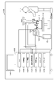
- FIG. 39 is a block diagram showing an example of the functional configuration of the camera head 11102 and CCU11201 shown in FIG. 38.
- the camera head 11102 includes a lens unit 11401, an image pickup unit 11402, a drive unit 11403, a communication unit 11404, and a camera head control unit 11405.
- CCU11201 has a communication unit 11411, an image processing unit 11412, and a control unit 11413.
- the camera head 11102 and CCU11201 are communicably connected to each other by a transmission cable 11400.
- the lens unit 11401 is an optical system provided at a connection portion with the lens barrel 11101.
- the observation light taken in from the tip of the lens barrel 11101 is guided to the camera head 11102 and incident on the lens unit 11401.
- the lens unit 11401 is configured by combining a plurality of lenses including a zoom lens and a focus lens.
- the image pickup unit 11402 is composed of an image pickup element.
- the image pickup element constituting the image pickup unit 11402 may be one (so-called single plate type) or a plurality (so-called multi-plate type).
- each image pickup element may generate an image signal corresponding to each of RGB, and a color image may be obtained by synthesizing them.
- the image pickup unit 11402 may be configured to have a pair of image pickup elements for acquiring image signals for the right eye and the left eye corresponding to 3D (Dimensional) display, respectively.
- the 3D display enables the operator 11131 to more accurately grasp the depth of the living tissue in the surgical site.
- a plurality of lens units 11401 may be provided corresponding to each image pickup element.
- the image pickup unit 11402 does not necessarily have to be provided on the camera head 11102.
- the image pickup unit 11402 may be provided inside the lens barrel 11101 immediately after the objective lens.
- the drive unit 11403 is composed of an actuator, and the zoom lens and focus lens of the lens unit 11401 are moved by a predetermined distance along the optical axis under the control of the camera head control unit 11405. As a result, the magnification and focus of the image captured by the image pickup unit 11402 can be adjusted as appropriate.
- the communication unit 11404 is configured by a communication device for transmitting and receiving various information to and from the CCU11201.
- the communication unit 11404 transmits the image signal obtained from the image pickup unit 11402 as RAW data to the CCU 11201 via the transmission cable 11400.
- the communication unit 11404 receives a control signal for controlling the drive of the camera head 11102 from the CCU 11201 and supplies the control signal to the camera head control unit 11405.
- the control signal includes, for example, information to specify the frame rate of the captured image, information to specify the exposure value at the time of imaging, and / or information to specify the magnification and focus of the captured image. Contains information about the condition.
- the image pickup conditions such as the frame rate, exposure value, magnification, and focus may be appropriately specified by the user, or may be automatically set by the control unit 11413 of CCU11201 based on the acquired image signal. good.
- the endoscope 11100 is equipped with a so-called AE (Auto Exposure) function, an AF (Auto Focus) function, and an AWB (Auto White Balance) function.
- the camera head control unit 11405 controls the drive of the camera head 11102 based on the control signal from the CCU 11201 received via the communication unit 11404.
- the communication unit 11411 is configured by a communication device for transmitting and receiving various information to and from the camera head 11102.
- the communication unit 11411 receives an image signal transmitted from the camera head 11102 via the transmission cable 11400.
- the communication unit 11411 transmits a control signal for controlling the drive of the camera head 11102 to the camera head 11102.
- Image signals and control signals can be transmitted by telecommunications, optical communication, or the like.
- the image processing unit 11412 performs various image processing on the image signal which is the RAW data transmitted from the camera head 11102.
- the control unit 11413 performs various controls related to the imaging of the surgical site and the like by the endoscope 11100 and the display of the captured image obtained by the imaging of the surgical site and the like. For example, the control unit 11413 generates a control signal for controlling the drive of the camera head 11102.
- control unit 11413 causes the display device 11202 to display an image captured by the surgical unit or the like based on the image signal processed by the image processing unit 11412.
- the control unit 11413 may recognize various objects in the captured image by using various image recognition techniques.
- the control unit 11413 detects a surgical tool such as forceps, a specific biological part, bleeding, mist when using the energy treatment tool 11112, etc. by detecting the shape, color, etc. of the edge of the object included in the captured image. Can be recognized.
- the control unit 11413 may superimpose and display various surgical support information on the image of the surgical unit by using the recognition result. By superimposing and displaying the surgery support information and presenting it to the surgeon 11131, the burden on the surgeon 11131 can be reduced and the surgeon 11131 can surely proceed with the surgery.
- the transmission cable 11400 connecting the camera head 11102 and CCU11201 is an electric signal cable corresponding to electric signal communication, an optical fiber corresponding to optical communication, or a composite cable thereof.
- the communication is performed by wire using the transmission cable 11400, but the communication between the camera head 11102 and the CCU11201 may be performed wirelessly.
- the above is an example of an endoscopic surgery system to which the technique according to the present disclosure can be applied.
- the technique according to the present disclosure can be suitably applied to the image pickup unit 11402 provided in the camera head 11102 of the endoscope 11100 among the configurations described above.
- the technique according to the present disclosure to the image pickup unit 11402, it is possible to obtain a photographed image having a high dynamic range, so that it is possible to provide a photographed image having a high dynamic range.
- the present disclosure may have the following structure.
- a comparator that performs temporal serial processing for comparison between a pixel signal according to the amount of incident light and a plurality of lamp signals that are time-shifted.
- a solid-state image sensor provided with a generation circuit that generates an image signal according to the result obtained by the comparison.
- a first lamp signal generation circuit that generates a first lamp signal, which is one of the plurality of lamp signals.
- the solid-state image pickup device according to (1) further comprising a second lamp signal generation circuit that generates a second lamp signal that is a lamp signal different from the first lamp signal among the plurality of lamp signals.
- the solid-state image sensor according to (1) wherein the pixel has a switching circuit for switching the conversion efficiency of the photoelectric conversion.
- (5) Further equipped with a lamp circuit that generates a specific lamp signal The solid-state imaging according to (1), wherein the comparator has a plurality of input circuits having different input capacities, and the specific lamp signal is input to the plurality of input circuits to acquire the plurality of lamp signals.
- the comparator is A first operation amplifier circuit for the pixel signal and a first lamp signal which is one of the plurality of lamp signals.
- a second operation amplifier circuit for the pixel signal and a second lamp signal which is a lamp signal different from the first lamp signal among the plurality of lamp signals.
- An output load circuit that is an output load of the first operation amplifier circuit and the second operation amplifier circuit, and The solid-state image pickup device according to any one of (1) to (5), which has any one of the first operation amplifier circuit and the second operation amplifier circuit and a connection circuit connecting the output load circuit.
- the comparator is A first operation amplifier circuit for the pixel signal and a first lamp signal which is one of the plurality of lamp signals.
- a second operation amplifier circuit for the pixel signal and a second lamp signal which is a lamp signal different from the first lamp signal among the plurality of lamp signals.
- An output load circuit that is an output load of the first operation amplifier circuit and the second operation amplifier circuit, and It has a connection circuit for connecting any of the first operation amplifier circuit and the second operation amplifier circuit to the output load circuit.
- the pixel is A photoelectric conversion unit that photoelectrically converts incident light, A charge holding unit that holds the charge transferred from the photoelectric conversion unit, and a charge holding unit.
- a transfer transistor that transfers charges from the photoelectric conversion unit to the charge holding unit, It has an additional capacitance section connected to the charge holding section via a switch element, and has an additional capacitance section.
- the switch element is turned on and the second operation amplification circuit is connected via the connection circuit.
- the solid-state imaging device according to (1) further comprising a control circuit for turning off the switch element when the circuit and the output load circuit are connected.
- the generation circuit is a first gradation signal generated by using a second lamp signal having a relatively low slope among the plurality of lamp signals, or a second lamp signal having a relatively high slope among the plurality of lamp signals. Which of the first gradation signal and the second gradation signal is used to generate the image signal based on the magnitude relationship between the second gradation signal generated by using the three lamp signals and a predetermined threshold value.
- the solid-state imaging device according to any one of (1) to (7).
- (9) Performing temporal serial processing for comparison between a pixel signal according to the amount of incident light and a plurality of lamp signals shifted in time.
- a signal processing method including generating an image signal according to the result obtained by the above comparison.
- (11) In addition to generating the pixel signal, generating a specific lamp signal using a lamp signal generation circuit
- (12) The first gradation signal generated by using the low slope lamp signal having a relatively low slope among the plurality of lamp signals, or the high slope lamp signal having a relatively high slope from the plurality of lamp signals is used.
- temporal serial processing is performed for comparison between a pixel signal according to the amount of incident light and a plurality of lamp signals shifted in time. Since the image signal was generated according to the result obtained by the above comparison, it is possible to select an appropriate analog gain signal in the subsequent processing of the comparator. As a result, since it is not necessary to provide a feedback circuit, it is possible to suppress the occurrence of a delay as in the case of providing a circuit for feeding back the detection result.
Landscapes
- Engineering & Computer Science (AREA)
- Multimedia (AREA)
- Signal Processing (AREA)
- Theoretical Computer Science (AREA)
- Transforming Light Signals Into Electric Signals (AREA)
- Studio Devices (AREA)
- Analogue/Digital Conversion (AREA)
Abstract
本開示の一実施の形態に係る固体撮像装置は、入射光量に応じた画素信号と、時間的にずれた複数のランプ信号との比較に対して時間的なシリアル処理を行う比較器と、上記比較により得られた結果に応じた画像信号を生成する生成回路とを備えている。
Description
本開示は、固体撮像装置および信号処理方法に関する。
被写体に高照度領域と低照度領域が混在している場合、低照度領域におけるS/Nを確保しつつ、ダイナミックレンジを拡大するためには、それぞれの領域に適したアナログゲインで読み出しを行う必要がある。この要求に対して、従来では、例えば、特許文献1に記載したように、各画素信号の大きさを独立に検出し、検出結果に応じて画素信号ごとにアナログゲインを設定することが提案されている。
しかし、特許文献1に記載の方法では、検出結果をフィードバックすることにより、アナログゲインを設定するため、検出結果の反映までに遅延が生じてしまうという問題があった。従って、遅延を抑制することの可能な固体撮像装置および信号処理方法を提供することが望ましい。
本開示の一実施の形態に係る固体撮像装置は、入射光量に応じた画素信号と、時間的にずれた複数のランプ信号との比較に対して時間的なシリアル処理を行う比較器と、上記比較により得られた結果に応じた画像信号を生成する生成回路とを備えている。
本開示の一実施の形態に係る信号処理方法は、以下の2つを含む。
(1)入射光量に応じた画素信号と、時間的にずれた複数のランプ信号との比較に対して時間的なシリアル処理を行うこと
(2)比較により得られた結果に応じた画像信号を生成すること
(1)入射光量に応じた画素信号と、時間的にずれた複数のランプ信号との比較に対して時間的なシリアル処理を行うこと
(2)比較により得られた結果に応じた画像信号を生成すること
本開示の一実施の形態に係る固体撮像装置および信号処理方法では、入射光量に応じた画素信号と、時間的にずれた複数のランプ信号との比較に対して時間的なシリアル処理が行われ、上記比較により得られた結果に応じた画像信号が生成される。このようなシリアル処理が行われることにより、シリアル処理後に、例えば、複数のランプ信号のうちの1つのランプ信号である第1ランプ信号を用いて生成された第1階調信号、もしくは、複数のランプ信号のうち第1ランプ信号とは異なるランプ信号である第2ランプ信号を用いて生成された第2階調信号と、所定の閾値との大小関係に基づいて、第1階調信号および第2階調信号のいずれを画像信号の生成に使用するか否かを決定することができる。このように、本開示では、比較器の後段の処理で、適切なアナログゲインの信号を選択することが可能となっているので、フィードバック回路を設ける必要がない。
以下、本開示の実施の形態について、図面を参照して詳細に説明する。なお、説明は以下の順序で行う。
1.実施の形態(固体撮像装置)…図1~図9
2.変形例(固体撮像装置)
変形例A:比較器内の入力容量を利用して
複数のランプ信号を生成する例…図10,図11
変形例B:センサ画素内の容量を利用して
複数のランプ信号を生成する例…図12~図27
変形例C:複数の画素回路を1つの読出し回路で共有することにより、
信号の大きさを変える例…図28~図34
3.適用例(撮像システム)…図35
4.応用例(移動体)
移動体への応用例…図36、図37
内視鏡手術システムへの応用例…図38、図39
1.実施の形態(固体撮像装置)…図1~図9
2.変形例(固体撮像装置)
変形例A:比較器内の入力容量を利用して
複数のランプ信号を生成する例…図10,図11
変形例B:センサ画素内の容量を利用して
複数のランプ信号を生成する例…図12~図27
変形例C:複数の画素回路を1つの読出し回路で共有することにより、
信号の大きさを変える例…図28~図34
3.適用例(撮像システム)…図35
4.応用例(移動体)
移動体への応用例…図36、図37
内視鏡手術システムへの応用例…図38、図39
<1.実施の形態>
[構成]
図1は、本開示の一実施の形態に係る固体撮像装置1の概略構成の一例を表す。固体撮像装置1は、例えば、CMOS(Complementary Metal Oxide Semiconductor)イメージセンサと、CMOSイメージセンサから得られた信号を処理する信号処理回路とを備えたカメラモジュールである。固体撮像装置1は、複数のセンサ画素11が設けられた画素アレイ部10を備えている。画素アレイ部10において、複数のセンサ画素11は、2次元(行列状に)配置されている。
[構成]
図1は、本開示の一実施の形態に係る固体撮像装置1の概略構成の一例を表す。固体撮像装置1は、例えば、CMOS(Complementary Metal Oxide Semiconductor)イメージセンサと、CMOSイメージセンサから得られた信号を処理する信号処理回路とを備えたカメラモジュールである。固体撮像装置1は、複数のセンサ画素11が設けられた画素アレイ部10を備えている。画素アレイ部10において、複数のセンサ画素11は、2次元(行列状に)配置されている。
画素アレイ部10は、複数のセンサ画素11と、複数の駆動配線と、複数のデータ出力線VSLとを有している。駆動配線は、センサ画素11に蓄積された電荷の出力を制御する制御信号が印加される配線であり、例えば、行方向に延在している。複数の駆動配線は、例えば、後述の垂直駆動回路21の出力端に接続されている。データ出力線VSLは、各センサ画素11から出力された画素信号を後述の周辺回路20に出力する配線であり、例えば、列方向に延在している。データ出力線VSLは、後述の読み出し回路13の出力端に接続されている。
センサ画素11は、例えば、図2に示したように、フォトダイオードPDを含む画素回路12と、画素回路12から画素信号を読み出す回路(読み出し回路13)とを含んで構成されている。フォトダイオードPDは、光電変換を行って受光量に応じた電荷を発生する素子である。画素回路12は、さらに、転送トランジスタTRGを有しており、転送トランジスタTRGをオンすることにより、フォトダイオードPDに蓄えられた電荷を読み出し回路13(後述のフローティングディフュージョンFD)に転送する。
読み出し回路13は、例えば、フローティングディフュージョンFDと、リセットトランジスタRSTと、増幅トランジスタAMPと、選択トランジスタSELとを有している。
フローティングディフュージョンFDは、転送トランジスタTRGを介してフォトダイオードPDから出力された電荷を一時的に保持する浮遊拡散領域である。フローティングディフュージョンFDには、例えば、リセットトランジスタRSTが接続されるとともに、増幅トランジスタAMPおよび選択トランジスタSELを介してデータ出力線VSLが接続されている。
リセットトランジスタRSTでは、ドレインが電源線VDDに接続され、ソースがフローティングディフュージョンFDに接続されている。リセットトランジスタRSTは、ゲート電極に印加される制御信号に応じて、フローティングディフュージョンFDを初期化(リセット)する。例えば、リセットトランジスタRSTがオンすると、フローティングディフュージョンFDの電位が電源線VDDの電位レベルにリセットされる。すなわち、フローティングディフュージョンFDの初期化が行われる。
増幅トランジスタAMPは、ゲート電極がフローティングディフュージョンFDに接続され、ドレインが電源線VDDに接続されており、フォトダイオードPDでの光電変換によって得られる電荷を読み出すソースフォロワ回路の入力部となる。すなわち、増幅トランジスタAMPは、ソースが選択トランジスタSELを介してデータ出力線VSLに接続されることにより、データ出力線VSLの一端に接続される定電流源とソースフォロワ回路を構成する。
選択トランジスタSELは、増幅トランジスタAMPのソースとデータ出力線VSLとの間に接続されており、選択トランジスタSELのゲート電極には、選択信号として制御信号が供給される。選択トランジスタSELは、制御信号がオンすると導通状態となり、導通状態となった選択トランジスタSELを含むセンサ画素11が選択状態となる。センサ画素11が選択状態になると、増幅トランジスタAMPから出力される画素信号がデータ出力線VSLを介してAD変換回路22に読み出される。
固体撮像装置1は、さらに、画素信号を処理する周辺回路20を備えている。周辺回路20は、画素アレイ部10から入力された画素信号に基づいて画像信号を生成し、外部に出力する。周辺回路20は、例えば、垂直駆動回路21、AD変換回路22、水平駆動回路23、システム制御回路24および出力回路25を有している。
垂直駆動回路21は、例えば、複数のセンサ画素11を所定の単位画素行ごとに順に選択する。「所定の単位画素行」とは、同一アドレスで画素選択可能な画素行を指している。AD変換回路22は、例えば、垂直駆動回路21によって選択された行の各センサ画素11から出力される画素信号に対して、相関二重サンプリング(Correlated Double Sampling:CDS)処理を施す。AD変換回路22は、例えば、CDS処理を施すことにより、画素信号の信号レベルを抽出し、各センサ画素11の受光量に応じた画素信号を保持する。AD変換回路22は、例えば、データ出力線VSLごとに、図3に示したようなADC220を有している。ADC220は、画素アレイ部10から列毎に出力されるアナログ信号(画素信号)をデジタル信号に変換して出力する。ADC220の内部構成については後に詳述するものとする。
水平駆動回路23は、例えば、シフトレジスタなどによって構成され、AD変換回路22における複数のADC220の列アドレスや列走査の制御を行う。水平駆動回路23による制御の下に、複数のADC220の各々でAD変換されたNビットのデジタル信号は順に出力回路25に読み出され、出力回路25を経由して画像信号(画像データ)として出力される。システム制御回路24は、例えば、周辺回路20内の各ブロック(垂直駆動回路21、AD変換回路22および水平駆動回路23)の駆動を制御する。
続いて、ADC220の内部構成について説明する。ADC220は、例えば、シングルスロープA/D変換器を含んでいる。シングルスロープA/D変換器は、例えば、図3に示したように、ランプ信号生成回路221と、スイッチ222と、比較器223と、カウンタ224と、スイッチ225と、メモリ226とを含んで構成されている。
ランプ信号生成回路221は、時間的にずれた複数のランプ信号(ランプ波形の信号)を生成する。ランプ信号生成回路221は、例えば、時間的にずれた2つのランプ信号(ランプ波形の信号)を生成する。時間的にずれた2つのランプ信号のうち一方のランプ信号は、時間的にずれた2つのランプ信号のうち他方のランプ信号と比べて相対的に低スロープのランプ信号(ランプ信号VrefH)である。時間的にずれた2つのランプ信号のうち他方のランプ信号は、ランプ信号VrefLと比べて相対的に高スロープのランプ信号(ランプ信号VrefL)である。スイッチ222は、ランプ信号生成回路221からランプ信号VrefLが出力されるときは、ランプ信号生成回路221の出力端子と、比較器223におけるランプ信号VrefLの入力端子とを互いに接続する。スイッチ222は、ランプ信号生成回路221からランプ信号VrefHが出力されるときは、ランプ信号生成回路221の出力端子と、比較器223におけるランプ信号VrefHの入力端子とを互いに接続する。
ランプ信号生成回路221は、例えば、図4に示したように、2つのランプ信号生成回路(LGランプ信号生成回路221A、HGランプ信号生成回路221B)を有していてもよい。この場合、LGランプ信号生成回路221Aの出力端子が比較器223の入力端子Bに接続され、HGランプ信号生成回路221Bの出力端子が比較器223の入力端子Cに接続されてもよい。
LGランプ信号生成回路221Aは、システム制御回路24から与えられるクロックに基づいて、HGランプ信号生成回路221Bと比べて相対的に低スロープのランプ信号を生成する。HGランプ信号生成回路221Bは、システム制御回路24から与えられるクロックに基づいて、LGランプ信号生成回路221Aと比べて相対的に高スロープのランプ信号を生成する。LGランプ信号生成回路221AおよびHGランプ信号生成回路221Bは、それぞれ、例えば、ランプ信号(ランプ波形の信号)を生成するDAC(デジタル-アナログ変換回路)を含んで構成されていてもよい。
比較器223は、n列目の各センサ画素11から出力される信号に応じたデータ出力線VSLの信号電圧Vinと、2つの信号生成回路(LGランプ信号生成回路221A、HGランプ信号生成回路221B)から供給されるランプ波形のランプ信号VrefH,VrefLとを比較する。比較器223は、例えば、ランプ信号VrefHもしくはランプ信号VrefLが信号電圧Vinよりも大なるときに出力が"H"レベルになり、ランプ信号VrefHもしくはランプ信号VrefLが信号電圧Vin以下のときに出力が"L"レベルになる。
比較器223は、入力容量、作動増幅トランジスタおよびAZスイッチを、比較器223に入力されるランプ信号の数(例えば2系統)だけ設けたパイプライン構成となっている。比較器223は、例えば、図5に示したように、作動増幅回路31(ランプ側回路31a,画素側回路31b)と、作動増幅回路32(ランプ側回路32a,画素側回路32b)とを有している。作動増幅回路31(ランプ側回路31a,画素側回路31b)は、画素信号(信号電圧Vin)と、HGランプ信号生成回路221Bのランプ信号VrefHとの差分を増幅する増幅回路である。作動増幅回路32(ランプ側回路32a,画素側回路32b)は、画素信号(信号電圧Vin)と、LGランプ信号生成回路221AのVrefLとの差分を増幅する増幅回路である。
ランプ側回路31aは、例えば、入力容量としてのキャパシタC4と、作動増幅トランジスタと、AZスイッチとを含んで構成されている。画素側回路31bは、例えば、入力容量としてのキャパシタC1と、作動増幅トランジスタと、AZスイッチとを含んで構成されている。ランプ側回路32aは、例えば、入力容量としてのキャパシタC3と、作動増幅トランジスタと、AZスイッチとを含んで構成されている。画素側回路32bは、例えば、入力容量としてのキャパシタC2と、作動増幅トランジスタと、AZスイッチとを含んで構成されている。
比較器223は、さらに、例えば、図5に示したように、出力負荷回路34と、接続回路33とを有している。出力負荷回路34は、作動増幅回路31(ランプ側回路31a,画素側回路31b)および作動増幅回路32(ランプ側回路32a,画素側回路32b)の出力負荷となる回路である。接続回路33は、作動増幅回路31(ランプ側回路31a,画素側回路31b)および作動増幅回路32(ランプ側回路32a,画素側回路32b)のいずれかと、出力負荷回路34とを接続する回路である。
比較器223には、3つの入力端子A,B,Cが設けられている。入力端子Aは、作動増幅回路31,32の画素側回路31b,32bの入力端子であり、データ出力線VSLに接続される。入力端子Bは、作動増幅回路32のランプ側回路32aの入力端子であり、ランプ信号生成回路221のうち、ランプ信号VrefLが出力される出力端子に接続される。入力端子Cは、作動増幅回路31のランプ側回路31aの入力端子であり、ランプ信号生成回路221のうち、ランプ信号VrefHが出力される出力端子に接続される。
カウンタ224は非同期カウンタであり、システム制御回路24から与えられる制御信号による制御の下に、システム制御回路24からクロックが与えられ、当該クロックに同期してダウン(DOWN)カウントまたはアップ(UP)カウントを行うことにより、比較器223での比較動作の開始から比較動作の終了までの比較期間を計測する。スイッチ225は、システム制御回路24から与えられる制御信号による制御の下に、ある行のセンサ画素11についてのカウンタ224のカウント動作が完了した時点でオン(閉)状態となって当該カウンタ224のカウント結果をメモリ226に転送する。このようにして、各センサ画素11からデータ出力線VSLを経由して列毎に供給されるアナログ信号が、複数のAD220における比較器223およびカウンタ224の各動作により、Nビットのデジタル信号に変換されてメモリ226に格納される。
[動作]
次に、本実施の形態に係る固体撮像装置1の動作について説明する。図6は、ADC220における各種波形の一例を表したものである。図7は、固体撮像装置1における信号処理手順の一例を表したものである。
次に、本実施の形態に係る固体撮像装置1の動作について説明する。図6は、ADC220における各種波形の一例を表したものである。図7は、固体撮像装置1における信号処理手順の一例を表したものである。
固体撮像装置1は、まず、ADC220のオートゼロ(AZ)を実行する(ステップS101)。具体的には、ADC220は、システム制御回路24による制御によって、比較器223の3つの入力端子A,B,Cを同電圧とするオートゼロ(AZ)動作を行う。ADC220は、例えば、システム制御回路24による制御によって、AZ,S0,S1にトランジスタのオン電圧を印可し、比較器223の3つの入力端子A,B,Cに与えられる電圧が互いに等しくなるように、キャパシタC1,C2,C3,C4をチャージする。
次に、固体撮像装置1は、リセット動作時(P相)の画素信号VinのAD変換値(D_high,D_low)を取得する。
具体的には、ADC220は、リセット動作時(リセット期間)において、システム制御回路24による制御によって、S0にトランジスタのオン電圧を印可するとともに、AZ,S1にトランジスタのオフ電圧を印可する。続いて、ランプ信号生成回路221はP相のランプ信号VrefHを比較器223の入力端子Cに入力する。このとき、データ出力線VSLには、リセット動作時に画素11から出力されたP相の画素信号Vinが与えられている。これにより、比較器223が入力端子Cを介してP相のランプ信号VrefHを取得し、入力端子Aを介してP相の画素信号Vinを取得する(ステップS102)。比較器223は、P相の画素信号VinがP相のランプ信号VrefHよりも小さい場合に、Hi(High)の比較結果信号COM_Outを出力し、P相の画素信号VinがP相のランプ信号VrefHよりも大きい場合に、Lo(Low)の比較結果信号COM_Outを出力する。比較器223は、比較結果信号COM_Outをカウンタ224に出力する。カウンタ224は、システム制御回路24から供給されるクロック信号に基づいて、Hiの比較結果信号COM_Outが供給されている間だけ、内部のカウンタをカウントアップする。カウント結果が、P相のAD変換値D_highとなる。スイッチ225は、カウント動作完了時点でオン状態となってP相のAD変換値D_highをメモリ226に格納する。このようにして、ADC220は、P相のAD変換値D_highを取得する(ステップS102)。
次に、ADC220は、リセット動作時(リセット期間)において、システム制御回路24による制御によって、S1にトランジスタのオン電圧を印可するとともに、AZ,S0にトランジスタのオフ電圧を印可する。続いて、ランプ信号生成回路221はP相のランプ信号VrefLを比較器223の入力端子Bに入力する。このとき、データ出力線VSLには、リセット動作時に画素11から出力されたP相の画素信号Vinが与えられている。これにより、比較器223が入力端子Bを介してP相のランプ信号VrefLを取得し、入力端子Aを介してP相の画素信号Vinを取得する(ステップS103)。比較器223は、P相の画素信号VinがP相のランプ信号VrefLよりも小さい場合に、Hi(High)の比較結果信号COM_Outを出力し、P相の画素信号VinがP相のランプ信号VrefLよりも大きい場合に、Lo(Low)の比較結果信号COM_Outを出力する。比較器223は、比較結果信号COM_Outをカウンタ224に出力する。カウンタ224は、システム制御回路24から供給されるクロック信号に基づいて、Hiの比較結果信号COM_Outが供給されている間だけ、内部のカウンタをカウントアップする。カウント結果が、P相のAD変換値D_lowとなる。スイッチ225は、カウント動作完了時点でオン状態となってP相のAD変換値D_lowをメモリ226に格納する。このようにして、ADC220は、P相のAD変換値D_lowを取得する(ステップS103)。
次に、固体撮像装置1は、信号出力時(D相)の画素信号VinのAD変換値(D_high,D_low)を取得する。
具体的には、ADC220は、信号出力時(信号出力期間)において、システム制御回路24による制御によって、S0にトランジスタのオン電圧を印可するとともに、AZ,S1にトランジスタのオフ電圧を印可する。続いて、ランプ信号生成回路221はD相のランプ信号VrefHを比較器223の入力端子Cに入力する。このとき、データ出力線VSLには、信号出力時に画素11から出力されたD相の画素信号Vinが与えられている。これにより、比較器223が入力端子Cを介してD相のランプ信号VrefHを取得し、入力端子Aを介してD相の画素信号Vinを取得する(ステップS104)。比較器223は、D相の画素信号VinがD相のランプ信号VrefHよりも小さい場合に、Hi(High)の比較結果信号COM_Outを出力し、D相の画素信号VinがD相のランプ信号VrefHよりも大きい場合に、Lo(Low)の比較結果信号COM_Outを出力する。比較器223は、比較結果信号COM_Outをカウンタ224に出力する。カウンタ224は、システム制御回路24から供給されるクロック信号に基づいて、Hiの比較結果信号COM_Outが供給されている間だけ、内部のカウンタをカウントアップする。カウント結果が、D相のAD変換値D_highとなる。スイッチ225は、カウント動作完了時点でオン状態となってD相のAD変換値D_highをメモリ226に格納する。このようにして、ADC220は、D相のAD変換値D_highを取得する(ステップS104)。
次に、ADC220は、信号出力時(信号出力期間)において、システム制御回路24による制御によって、S1にトランジスタのオン電圧を印可するとともに、AZ,S0にトランジスタのオフ電圧を印可する。続いて、ランプ信号生成回路221はD相のランプ信号VrefLを比較器223の入力端子Bに入力する。このとき、データ出力線VSLには、信号出力時に画素11から出力されたD相の画素信号Vinが与えられている。これにより、比較器223が入力端子Bを介してD相のランプ信号VrefLを取得し、入力端子Aを介してD相の画素信号Vinを取得する(ステップS105)。比較器223は、D相の画素信号VinがD相のランプ信号VrefLよりも小さい場合に、Hi(High)の比較結果信号COM_Outを出力し、D相の画素信号VinがD相のランプ信号VrefLよりも大きい場合に、Lo(Low)の比較結果信号COM_Outを出力する。比較器223は、比較結果信号COM_Outをカウンタ224に出力する。カウンタ224は、システム制御回路24から供給されるクロック信号に基づいて、Hiの比較結果信号COM_Outが供給されている間だけ、内部のカウンタをカウントアップする。カウント結果が、D相のAD変換値D_lowとなる。スイッチ225は、カウント動作完了時点でオン状態となってD相のAD変換値D_lowをメモリ226に格納する。このようにして、ADC220は、D相のAD変換値D_lowを取得する(ステップS105)。
次に、ADC220は、D相のAD変換値D_highとP相のAD変換値D_highとの差分を取得し、取得した差分を階調信号Dout_highとしてメモリ226に格納する。さらに、ADC220は、D相のAD変換値D_lowとP相のAD変換値D_lowとの差分を取得し、取得した差分を階調信号Dout_lowとしてメモリ226に格納する。このようにして、ADC220は、階調信号Dout_high,Dout_lowを取得する(ステップS106)。AD変換回路22は、階調信号Dout_high,Dout_lowを、水平駆動回路23の制御の下に、各ADC220のメモリ307から読み出し、水平出力線を介して出力回路25に出力する。
出力回路25は、階調信号Dout_highが閾値Dthよりも大きいか否か判定する(ステップS107)。その結果、階調信号Dout_highが閾値Dthよりも大きい場合には(ステップS107;Y)、出力回路25は、閾値Dthよりも大きい階調信号Dout_highに対応する画素列の階調信号Dout_lowを選択し、出力する(ステップS108)。一方、階調信号Dout_highが閾値Dth以下の場合には(ステップS107;N)、出力回路25は、閾値Dth以下の階調信号Dout_highを選択し、出力する(ステップS109)。このようにして、固体撮像装置1におけるAD変換が行われる。
[効果]
次に、本実施の形態に係る固体撮像装置1の効果について説明する。
次に、本実施の形態に係る固体撮像装置1の効果について説明する。
被写体に高照度領域と低照度領域が混在している場合、低照度領域におけるS/Nを確保しつつ、ダイナミックレンジを拡大するためには、それぞれの領域に適したアナログゲインで読み出しを行う必要がある。この要求に対して、例えば、図8に示したようなADC300が考えられる。ADC300は、例えば、2つのランプ信号生成回路301,302と、スイッチ303と、比較器304と、カウンタ305と、スイッチ306と、メモリ307と、照度判定部308を含んで構成されている。
2つのランプ信号生成回路301,302は、スロープの互いに異なる2つのランプ信号を生成する回路である。一方のランプ信号生成回路301の出力端子がスイッチ303の一方の入力端子に接続され、他方のランプ信号生成回路302の出力端子がスイッチ303の他方の入力端子に接続されている。比較器304の一方の入力端子Dがデータ出力線VSLに接続され、比較器304の他方の入力端子Eがスイッチ303の出力端子に接続されている。比較器304は、入力端子Dに入力される画素信号Vinと、入力端子Eに入力されるランプ信号との比較結果(COM_Out)を出力する。照度判定部308は、比較結果(COM_Out)に基づいて、2つのランプ信号生成回路301,302のいずれかを選択する選択信号をスイッチ303に出力する。照度判定部308からの選択信号によって選択されたランプ信号が比較器304の入力端子Eに入力される。
ADC300では、各画素信号の大きさ(COM_Out)が独立に検出され、検出結果に応じて画素信号ごとにアナログゲインが設定される。しかし、この方法では、検出結果をフィードバックすることにより、アナログゲインを設定するため、検出結果の反映までに遅延が生じてしまうという問題があった。
一方、本実施の形態では、入射光量に応じた画素信号と、時間的にずれた2つのランプ信号VrefH,VrefLとの比較に対して時間的なシリアル処理が行われ、上記比較により得られた結果に応じた画像信号が生成される。このようなシリアル処理が行われることにより、シリアル処理後に、例えば、ランプ信号VrefHを用いて生成された階調信号D_highと、所定の閾値Dthとの大小関係に基づいて、階調信号D_highおよび階調信号D_lowのいずれを画像信号の生成に使用するか否かを決定することができる。このように、本実施の形態では、比較器223の後段の処理で、適切なアナログゲインの信号を選択することが可能となっているので、フィードバック回路を設ける必要がない。その結果、検出結果をフィードバックする回路を設けた場合のような遅延が生じるのを抑制することができる。
また、本実施の形態では、2つのランプ信号生成回路221A,221Bが設けられている。これにより、一方のランプ信号生成回路221Aと、他方のランプ信号生成回路221Bとで、ランプ信号を時間的にずらしたり、スロープを互いに異ならせたりすることが可能となる。その結果、例えば、一方のランプ信号生成回路221Bを用いて生成された階調信号D_high、および他方のランプ信号生成回路221Aを用いて生成された階調信号D_lowのいずれを画像信号の生成に使用するか否かを決定することができる。このように、本実施の形態では、比較器223の後段の処理で、適切なアナログゲインの信号を選択することが可能となっているので、フィードバック回路を設ける必要がない。その結果、検出結果をフィードバックする回路を設けた場合のような遅延が生じるのを抑制することができる。
また、本実施の形態では、比較器223において、画素信号Vinとランプ信号VrefHとに対する作動増幅回路31と、画素信号Vinとランプ信号VrefLとに対する作動増幅回路32と、作動増幅回路31,32のいずれかと、作動増幅回路31,32の出力付加となる出力負荷回路34とを接続する接続回路33が設けられている。これにより、1つの比較器223で、画素信号Vinと、時間的にずれた2つのランプ信号VrefL,VrefHとの比較に対して時間的なシリアル処理を行うことができる。このようなシリアル処理を行うことにより、シリアル処理後に、例えば、ランプ信号VrefHを用いて生成された階調信号D_highと、所定の閾値Dthとの大小関係に基づいて、階調信号D_highおよび階調信号D_lowのいずれを画像信号の生成に使用するか否かを決定することができる。このように、本実施の形態では、比較器223の後段の処理で、適切なアナログゲインの信号を選択することが可能となっているので、フィードバック回路を設ける必要がない。その結果、検出結果をフィードバックする回路を設けた場合のような遅延が生じるのを抑制することができる。
また、本実施の形態では、階調信号Dout_highと、所定の閾値Dthとの大小関係に基づいて、階調信号Dout_highおよび階調信号Dout_lowのいずれを画像信号の生成に使用するか否かが決定される。このように、本実施の形態では、比較器223の後段の処理で、適切なアナログゲインの信号を選択することが可能となっているので、フィードバック回路を設ける必要がない。その結果、検出結果をフィードバックする回路を設けた場合のような遅延が生じるのを抑制することができる。
<2.変形例>
次に、上記実施の形態に係る固体撮像装置1の変形例について説明する。
次に、上記実施の形態に係る固体撮像装置1の変形例について説明する。
[変形例A]
上記実施の形態に係る固体撮像装置1において、例えば、図9に示したように、ランプ信号生成回路221の代わりに、特定のランプ信号Vrefを生成するランプ信号生成回路227が設けられていてもよい。この場合、ランプ信号生成回路227の出力端子が比較器223の2つの入力端子B,Cに接続されていてもよい。
上記実施の形態に係る固体撮像装置1において、例えば、図9に示したように、ランプ信号生成回路221の代わりに、特定のランプ信号Vrefを生成するランプ信号生成回路227が設けられていてもよい。この場合、ランプ信号生成回路227の出力端子が比較器223の2つの入力端子B,Cに接続されていてもよい。
図10は、本変形例に係る固体撮像装置1における比較器223の回路構成例を表したものである。本変形例において、比較器223は、入力容量の互いに異なる2つの入力回路35,36を有している。一方の入力回路35は入力端子Bに設けられており、他方の入力回路36は入力端子Cに設けられている。入力回路35は、例えば、入力端子Bに直列に接続されたキャパシタC3と、一端がキャパシタC3の、入力端子Bとは反対側の端子に接続されたキャパシタC5とを含んで構成されている。入力回路36は、例えば、入力端子Cに直列に接続されたキャパシタC4を含んで構成されている。
このように、本変形例では、入力容量の互いに異なる2つの入力回路35,36が比較器223に設けられている。これにより、共通のランプ信号Vrefが入力端子B,Cに入力されることにより、入力回路35を介して作動増幅回路32に入力されるランプ信号のスロープと、入力回路36を介して作動増幅回路31に入力されるランプ信号のスロープとを互いに異ならせることができる。また、例えば、図6に示したように、システム制御回路24による制御によって、AZ,S0,S1の信号波形を制御することにより、作動増幅回路31の動作開始タイミングと、作動増幅回路32の動作開始タイミングとを時間的にずらすことができる。これにより、本変形例でも、比較器223において、画素信号Vinと、時間的にずれた複数のランプ信号との比較に対して時間的なシリアル処理を行うことができる。従って、複数のランプ信号生成回路を設けなくても、上記実施の形態と同様の効果を得ることができる。
[変形例B]
上記変形例Aにおいて、センサ画素11の読み出し回路13が、光電変換の変換効率を切り替える切り替え回路を有していてもよい。切り替え回路は、例えば、図11に示したように、リセットトランジスタTSTのソース・ドレイン端子と、増幅トランジスタAMPのゲート端子との間に設けられた切り替えトラジスタFDGと、一端が切り替えトラジスタFDGの、リセットトランジスタTST側のソース・ドレイン端子に接続されたキャパシタCとを含んで構成されている。
上記変形例Aにおいて、センサ画素11の読み出し回路13が、光電変換の変換効率を切り替える切り替え回路を有していてもよい。切り替え回路は、例えば、図11に示したように、リセットトランジスタTSTのソース・ドレイン端子と、増幅トランジスタAMPのゲート端子との間に設けられた切り替えトラジスタFDGと、一端が切り替えトラジスタFDGの、リセットトランジスタTST側のソース・ドレイン端子に接続されたキャパシタCとを含んで構成されている。
図12は、本変形例に係る固体撮像装置1における比較器223の回路構成例を表したものである。本変形例において、比較器223の2つの入力端子B,Cは、配線を介して互いに接続されている。本変形例では、比較器223に入力されるAZ信号は、AZ0,AZ1の2種類となっている。AZ0は、パイプライン構成における一方の系統のためのAZ信号である。AZ1は、パイプライン構成における他方の系統のためのAZ信号である。
本変形例では、ランプ側回路31aは、例えば、入力容量としてのキャパシタC4と、作動増幅トランジスタと、AZ1スイッチとを含んで構成されている。画素側回路31bは、例えば、入力容量としてのキャパシタC1と、作動増幅トランジスタと、AZ1スイッチとを含んで構成されている。ランプ側回路32aは、例えば、入力容量としてのキャパシタC3と、作動増幅トランジスタと、AZ0スイッチとを含んで構成されている。画素側回路32bは、例えば、入力容量としてのキャパシタC2と、作動増幅トランジスタと、AZ0スイッチとを含んで構成されている。
次に、本変形例に係る固体撮像装置1の動作について説明する。図13は、固体撮像装置1における各種波形の一例を表したものである。図14は、固体撮像装置1における信号処理手順の一例を表したものである。
固体撮像装置1は、まず、ADC220におけるAZ0のオートゼロ(AZ)を実行する(ステップS201)。具体的には、ADC220は、システム制御回路24による制御によって、比較器223の2つの入力端子A,Bを同電圧とするオートゼロ(AZ)動作を行う。ADC220は、例えば、システム制御回路24による制御によって、AZ0,S0,S1にトランジスタのオン電圧を印可し、比較器223の2つの入力端子A,Bに与えられる電圧が互いに等しくなるように、キャパシタC2,C3をチャージする。
次に、固体撮像装置1は、リセット動作時(P相)の画素信号VinのAD変換値(D_low)を取得する。
具体的には、ADC220は、リセット動作時(リセット期間)において、システム制御回路24による制御によって、S0にトランジスタのオン電圧を印可するとともに、AZ0,AZ1,S1にトランジスタのオフ電圧を印可する。続いて、ランプ信号生成回路227はP相のランプ信号Vrefを比較器223の入力端子Bに入力する。このとき、変換トランジスタFDGがオンすることによって変換効率が切り替えられており、データ出力線VSLには、切り替え後の変換効率(低い変換効率)に応じたP相の画素信号Vin’が与えられている。これにより、比較器223が入力端子Bを介してP相のランプ信号Vrefを取得し、入力端子Aを介してP相の画素信号Vin’を取得する(ステップS202)。比較器223は、P相の画素信号Vin’がP相のランプ信号Vrefよりも小さい場合に、Hi(High)の比較結果信号COM_Outを出力し、P相の画素信号Vin’がP相のランプ信号Vrefよりも大きい場合に、Lo(Low)の比較結果信号COM_Outを出力する。比較器223は、比較結果信号COM_Outをカウンタ224に出力する。カウンタ224は、システム制御回路24から供給されるクロック信号に基づいて、Hiの比較結果信号COM_Outが供給されている間だけ、内部のカウンタをカウントアップする。カウント結果が、P相のAD変換値D_lowとなる。スイッチ225は、カウント動作完了時点でオン状態となってP相のAD変換値D_lowをメモリ226に格納する。このようにして、ADC220は、P相のAD変換値D_lowを取得する(ステップS202)。
次に、固体撮像装置1は、ADC220におけるAZ1のオートゼロ(AZ)を実行する(ステップS203)。具体的には、ADC220は、システム制御回路24による制御によって、比較器223の2つの入力端子A,Cを同電圧とするオートゼロ(AZ)動作を行う。ADC220は、例えば、システム制御回路24による制御によって、AZ1,S1にトランジスタのオン電圧を印可し、比較器223の2つの入力端子A,Cに与えられる電圧が互いに等しくなるように、キャパシタC1,C4をチャージする。
次に、ADC220は、リセット動作時(リセット期間)において、システム制御回路24による制御によって、S1にトランジスタのオン電圧を印可するとともに、AZ0,AZ1,S0にトランジスタのオフ電圧を印可する。続いて、ランプ信号生成回路227はP相のランプ信号Vrefを比較器223の入力端子Cに入力する。このとき、変換トランジスタFDGがオフしているため変換効率が元の状態に戻っており、データ出力線VSLには、元の状の変換効率に応じたP相の画素信号Vinが与えられている。これにより、比較器223が入力端子Cを介してP相のランプ信号Vrefを取得し、入力端子Aを介してP相の画素信号Vinを取得する(ステップS204)。比較器223は、P相の画素信号VinがP相のランプ信号Vrefよりも小さい場合に、Hi(High)の比較結果信号COM_Outを出力し、P相の画素信号VinがP相のランプ信号Vrefよりも大きい場合に、Lo(Low)の比較結果信号COM_Outを出力する。比較器223は、比較結果信号COM_Outをカウンタ224に出力する。カウンタ224は、システム制御回路24から供給されるクロック信号に基づいて、Hiの比較結果信号COM_Outが供給されている間だけ、内部のカウンタをカウントアップする。カウント結果が、P相のAD変換値D_highとなる。スイッチ225は、カウント動作完了時点でオン状態となってP相のAD変換値D_highをメモリ226に格納する。このようにして、ADC220は、P相のAD変換値D_highを取得する(ステップS204)。
次に、固体撮像装置1は、信号出力時(D相)の画素信号VinのAD変換値(D_high,D_low)を取得する。
具体的には、ADC220は、信号出力時(信号出力期間)において、システム制御回路24による制御によって、S1にトランジスタのオン電圧を印可するとともに、AZ0,AZ1,S0にトランジスタのオフ電圧を印可する。続いて、ランプ信号生成回路227はD相のランプ信号Vrefを比較器223の入力端子Cに入力する。このとき、変換トランジスタFDGがオフしているため変換効率が元の状態に戻っており、データ出力線VSLには、元の状の変換効率に応じたP相の画素信号Vinが与えられている。これにより、比較器223が入力端子Cを介してD相のランプ信号Vrefを取得し、入力端子Aを介してD相の画素信号Vinを取得する(ステップS205)。比較器223は、D相の画素信号VinがD相のランプ信号Vrefよりも小さい場合に、Hi(High)の比較結果信号COM_Outを出力し、D相の画素信号VinがD相のランプ信号Vrefよりも大きい場合に、Lo(Low)の比較結果信号COM_Outを出力する。比較器223は、比較結果信号COM_Outをカウンタ224に出力する。カウンタ224は、システム制御回路24から供給されるクロック信号に基づいて、Hiの比較結果信号COM_Outが供給されている間だけ、内部のカウンタをカウントアップする。カウント結果が、D相のAD変換値D_highとなる。スイッチ225は、カウント動作完了時点でオン状態となってD相のAD変換値D_highをメモリ226に格納する。このようにして、ADC220は、D相のAD変換値D_highを取得する(ステップS205)。
次に、ADC220は、信号出力時(信号出力期間)において、システム制御回路24による制御によって、S0にトランジスタのオン電圧を印可するとともに、AZ0,AZ1,S1にトランジスタのオフ電圧を印可する。続いて、ランプ信号生成回路227はD相のランプ信号Vrefを比較器223の入力端子Bに入力する。このとき、変換トランジスタFDGがオンすることによって変換効率が切り替えられており、データ出力線VSLには、切り替え後の変換効率(低い変換効率)に応じたP相の画素信号Vin’が与えられている。これにより、比較器223が入力端子Bを介してD相のランプ信号Vrefを取得し、入力端子Aを介してD相の画素信号Vinを取得する(ステップS206)。比較器223は、D相の画素信号VinがD相のランプ信号Vrefよりも小さい場合に、Hi(High)の比較結果信号COM_Outを出力し、D相の画素信号VinがD相のランプ信号Vrefよりも大きい場合に、Lo(Low)の比較結果信号COM_Outを出力する。比較器223は、比較結果信号COM_Outをカウンタ224に出力する。カウンタ224は、システム制御回路24から供給されるクロック信号に基づいて、Hiの比較結果信号COM_Outが供給されている間だけ、内部のカウンタをカウントアップする。カウント結果が、D相のAD変換値D_lowとなる。スイッチ225は、カウント動作完了時点でオン状態となってD相のAD変換値D_lowをメモリ226に格納する。このようにして、ADC220は、D相のAD変換値D_lowを取得する(ステップS206)。
次に、ADC220は、D相のAD変換値D_highとP相のAD変換値D_highとの差分を取得し、取得した差分を階調信号Dout_highとしてメモリ226に格納する。さらに、ADC220は、D相のAD変換値D_lowとP相のAD変換値D_lowとの差分を取得し、取得した差分を階調信号Dout_lowとしてメモリ226に格納する。このようにして、ADC220は、階調信号Dout_high,Dout_lowを取得する(ステップS207)。AD変換回路22は、階調信号Dout_high,Dout_lowを、水平駆動回路23の制御の下に、各ADC220のメモリ307から読み出し、水平出力線を介して出力回路25に出力する。
出力回路25は、階調信号Dout_highが閾値Dthよりも大きいか否か判定する(ステップS208)。その結果、階調信号Dout_highが閾値Dthよりも大きい場合には(ステップS208;Y)、出力回路25は、閾値Dthよりも大きい階調信号Dout_highに対応する画素列の検出信号Dout_lowを選択し、出力する(ステップS209)。一方、検出信号Dout_highが閾値Dth以下の場合には(ステップS208;N)、出力回路25は、閾値Dth以下の階調信号Dout_highを選択し、出力する(ステップS210)。このようにして、固体撮像装置1におけるAD変換が行われる。
次に、本変形例に係る固体撮像装置1の効果について説明する。
本変形例では、光電変換の変換効率を切り替える切り替え回路がセンサ画素11に設けられている。これにより、切り替え回路で光電変換の変換効率を切り替えることにより、切り替え後の変換効率(低い変換効率)に応じたP相の画素信号Vin’と、P相のランプ信号Vrefとに基づいてP相のAD変換値D_lowが得られ、切り替え前の変換効率(高い変換効率)に応じたP相の画素信号Vinと、P相のランプ信号Vrefとに基づいてP相のAD変換値D_highが得られる。さらに、切り替え前の変換効率(高い変換効率)に応じたP相の画素信号Vinと、D相のランプ信号Vrefとに基づいてD相のAD変換値D_highが得られ、切り替え後の変換効率(低い変換効率)に応じたD相の画素信号Vin’と、D相のランプ信号Vrefとに基づいてD相のAD変換値D_lowが得られる。このようなシリアル処理が行われた後に、D相のAD変換値D_highとP相のAD変換値D_highとの差分から階調信号Dout_highが得られ、D相のAD変換値D_lowとP相のAD変換値D_lowとの差分から階調信号Dout_lowが得られる。その後、例えば、階調信号Dout_highと、所定の閾値Dthとの大小関係に基づいて、階調信号D_highおよび階調信号D_lowのいずれを画像信号の生成に使用するか否かが決定される。このように、本変形例では、比較器223の後段の処理で、適切なアナログゲインの信号を選択することが可能となっているので、フィードバック回路を設ける必要がない。その結果、検出結果をフィードバックする回路を設けた場合のような遅延が生じるのを抑制することができる。
また、本変形例では、接続回路33を介して作動増幅回路32と出力負荷回路34とが接続されているときに、変換トランジスタFDGがオンされ、接続回路33を介して作動増幅回路31と出力負荷回路34とが接続されているときに、変換トランジスタFDGがオフされる。このように、比較器223におけるパイプラインの切り替えと、センサ画素11における光電変換の変換効率の切り替えとを同期させることにより、画素信号Vin,Vin’と、時間的にずれた複数のランプ信号Vrefとの比較に対して時間的なシリアル処理を行うことができる。従って、複数のランプ信号生成回路を設けなくても、上記実施の形態と同様の効果を得ることができる。
[変形例C]
上記変形例Bにおいて、切り替え回路が、例えば、図15、図16に示したように、直列に接続されるとともに互いに独立に制御される複数の切り替えトラジスタFDGを有していてもよい。このとき、一端が、互いに隣接する2つの切り替えトラジスタFDGのソース・ドレイン端子に接続されたキャパシタCが設けられていてもよい。本変形例では、システム制御回路24が、例えば、各切り替えトラジスタFDGのゲートに対して独立にパルスを印可することにより、複数の切り替えトラジスタFDGのオンオフ(ひいては、光電変換の変換効率の切り替え)を行う。
上記変形例Bにおいて、切り替え回路が、例えば、図15、図16に示したように、直列に接続されるとともに互いに独立に制御される複数の切り替えトラジスタFDGを有していてもよい。このとき、一端が、互いに隣接する2つの切り替えトラジスタFDGのソース・ドレイン端子に接続されたキャパシタCが設けられていてもよい。本変形例では、システム制御回路24が、例えば、各切り替えトラジスタFDGのゲートに対して独立にパルスを印可することにより、複数の切り替えトラジスタFDGのオンオフ(ひいては、光電変換の変換効率の切り替え)を行う。
システム制御回路24が、例えば、図17に示したように、3つの切り替えトラジスタFDGを全てオンさせる。これにより、3つのキャパシタCがフローティングディフュージョンFDに並列に接続されるので、接続されたキャパシタCの数に応じて光電変換の変換効率が小さくなる。システム制御回路24が、例えば、図18に示したように、3つの切り替えトラジスタFDGのうち、増幅トランジスタAMP側の2つの切り替えトランジスタFDGだけをオンさせる。これにより、2つのキャパシタCがフローティングディフュージョンFDに並列に接続されるので、接続されたキャパシタCの数に応じて光電変換の変換効率が小さくなる。
システム制御回路24が、例えば、図19に示したように、3つの切り替えトラジスタFDGのうち、両端の2つの切り替えトランジスタFDGだけをオンさせる。これにより、増幅トランジスタAMP側の1つのキャパシタCがフローティングディフュージョンFDに並列に接続されるので、接続されたキャパシタCの数に応じて光電変換の変換効率が小さくなる。システム制御回路24が、例えば、図20に示したように、3つの切り替えトラジスタFDGのうち、リセットトランジスタRST側の2つの切り替えトランジスタFDGだけをオンさせる。このとき、キャパシタCはフローティングディフュージョンFDに接続されないので、光電変換の変換効率は切り替え前と特段変わらない。
[変形例D]
上記変形例Bにおいて、切り替え回路が、例えば、図21に示したように、一端(ソース・ドレイン端子)がリセットトランジスタRSTのソース・ドレイン端子および増幅トランジスタAMPのゲート端子に接続された切り替えトランジスタFDGを有していてもよい。このとき、切り替えトランジスタFDGの他端(ソース・ドレイン端子)にキャパシタCが接続されていてもよい。本変形例では、システム制御回路24が、切り替えトランジスタFDGをオンさせることにより、切り替えトランジスタFDGを介してキャパシタCがフローティングディフュージョンFDに並列に接続される。これにより、接続されたキャパシタCの数に応じて光電変換の変換効率が小さくなる。
上記変形例Bにおいて、切り替え回路が、例えば、図21に示したように、一端(ソース・ドレイン端子)がリセットトランジスタRSTのソース・ドレイン端子および増幅トランジスタAMPのゲート端子に接続された切り替えトランジスタFDGを有していてもよい。このとき、切り替えトランジスタFDGの他端(ソース・ドレイン端子)にキャパシタCが接続されていてもよい。本変形例では、システム制御回路24が、切り替えトランジスタFDGをオンさせることにより、切り替えトランジスタFDGを介してキャパシタCがフローティングディフュージョンFDに並列に接続される。これにより、接続されたキャパシタCの数に応じて光電変換の変換効率が小さくなる。
[変形例E]
上記変形例Dにおいて、切り替え回路が、例えば、図22、図23に示したように、互いに並列に接続されるとともに互いに独立に制御される複数の切り替えトラジスタFDGを有していてもよい。このとき、一端が、互いに隣接する2つの切り替えトラジスタFDGのソース・ドレイン端子に接続されたキャパシタCが設けられていてもよい。本変形例では、システム制御回路24が、例えば、各切り替えトラジスタFDGのゲートに対して独立にパルスを印可することにより、複数の切り替えトラジスタFDGのオンオフ(ひいては、光電変換の変換効率の切り替え)を行う。
上記変形例Dにおいて、切り替え回路が、例えば、図22、図23に示したように、互いに並列に接続されるとともに互いに独立に制御される複数の切り替えトラジスタFDGを有していてもよい。このとき、一端が、互いに隣接する2つの切り替えトラジスタFDGのソース・ドレイン端子に接続されたキャパシタCが設けられていてもよい。本変形例では、システム制御回路24が、例えば、各切り替えトラジスタFDGのゲートに対して独立にパルスを印可することにより、複数の切り替えトラジスタFDGのオンオフ(ひいては、光電変換の変換効率の切り替え)を行う。
システム制御回路24が、例えば、図24に示したように、3つの切り替えトラジスタFDGを全てオンさせる。これにより、3つのキャパシタCがフローティングディフュージョンFDに並列に接続されるので、接続されたキャパシタCの数に応じて光電変換の変換効率が小さくなる。システム制御回路24が、例えば、図25に示したように、3つの切り替えトラジスタFDGのうち、増幅トランジスタAMP側の2つの切り替えトランジスタFDGだけをオンさせる。これにより、2つのキャパシタCがフローティングディフュージョンFDに並列に接続されるので、接続されたキャパシタCの数に応じて光電変換の変換効率が小さくなる。
システム制御回路24が、例えば、図26に示したように、3つの切り替えトラジスタFDGのうち、増幅トランジスタAMP側の1つの切り替えトランジスタFDGだけをオンさせる。これにより、増幅トランジスタAMP側の1つのキャパシタCがフローティングディフュージョンFDに並列に接続されるので、接続されたキャパシタCの数に応じて光電変換の変換効率が小さくなる。システム制御回路24が、例えば、図27に示したように、3つの切り替えトラジスタFDG全てをオフさせる。このとき、キャパシタCはフローティングディフュージョンFDに接続されないので、光電変換の変換効率は切り替え前と特段変わらない。
[変形例F]
上記実施の形態および変形例A,Bに係るセンサ画素11において、複数の画素回路12が1つの読み出し回路13を共有してもよい。例えば、図28に示したように、2つの画素回路12が1つの読み出し回路13を共有してもよい。また、例えば、図29に示したように、4つの画素回路12が1つの読み出し回路13を共有してもよい。また、例えば、図30に示したように、多数の画素回路12が1つの読み出し回路13を共有してもよい。
上記実施の形態および変形例A,Bに係るセンサ画素11において、複数の画素回路12が1つの読み出し回路13を共有してもよい。例えば、図28に示したように、2つの画素回路12が1つの読み出し回路13を共有してもよい。また、例えば、図29に示したように、4つの画素回路12が1つの読み出し回路13を共有してもよい。また、例えば、図30に示したように、多数の画素回路12が1つの読み出し回路13を共有してもよい。
このとき、垂直駆動回路21が、例えば、図31に示したように、4つの画素回路12のうち1つの画素回路12に含まれる転送トランジスタTRGをオンさせる。これにより、1つの画素回路12からの電荷がフローティングディフュージョンFDに転送される。また、垂直駆動回路21が、例えば、図32に示したように、4つの画素回路12のうち2つの画素回路12に含まれる転送トランジスタTRGをオンさせる。これにより、2つの画素回路12からの電荷がフローティングディフュージョンFDに転送されるので、1つの画素回路12からの電荷がフローティングディフュージョンFDに転送される場合と比べて、フローティングディフュージョンFDに蓄積される電荷量を増やすことができる。その結果、電荷量が増えた分だけ、信号ゲインを大きくすることができる。
垂直駆動回路21が、例えば、図33に示したように、4つの画素回路12のうち3つの画素回路12に含まれる転送トランジスタTRGをオンさせる。これにより、3つの画素回路12からの電荷がフローティングディフュージョンFDに転送されるので、2つの画素回路12からの電荷がフローティングディフュージョンFDに転送される場合と比べて、フローティングディフュージョンFDに蓄積される電荷量を増やすことができる。その結果、電荷量が増えた分だけ、信号ゲインを大きくすることができる。
垂直駆動回路21が、例えば、図34に示したように、4つの画素回路12全てに含まれる転送トランジスタTRGをオンさせる。これにより、4つの画素回路12からの電荷がフローティングディフュージョンFDに転送されるので、3つの画素回路12からの電荷がフローティングディフュージョンFDに転送される場合と比べて、フローティングディフュージョンFDに蓄積される電荷量を増やすことができる。その結果、電荷量が増えた分だけ、信号ゲインを大きくすることができる。
<3.適用例>
次に、上記実施の形態に係る固体撮像装置1の適用例について説明する。
次に、上記実施の形態に係る固体撮像装置1の適用例について説明する。
図35は、上記実施の形態およびその変形例に係る固体撮像装置1を備えた撮像システム2の概略構成の一例を表したものである。撮像システム2は、例えば、光学系410と、シャッタ機構420と、固体撮像装置1と、信号処理回路430と、表示部440とを備えている。
光学系410は、被写体からの像光(入射光)を固体撮像装置1の撮像面上に結像させる。これにより、固体撮像装置1内に、一定期間、信号電荷が蓄積される。シャッタ機構420は、開閉することにより、固体撮像装置1への光照射期間及び遮光期間を制御する。固体撮像装置1は、光学系410から入射された像光(入射光)を受光し、受光した像光(入射光)に応じた画像データを信号処理回路430に出力する。信号処理回路430は、固体撮像装置1から入力された画像データを処理して、映像データを生成する。信号処理回路430は、さらに、生成した映像データに対応する映像信号を生成し、表示部440に出力する。表示部440は、信号処理回路230から入力された映像信号に基づく映像を表示する。
本適用例では、上記実施の形態およびその変形例に係る固体撮像装置1が撮像システム2に適用される。これにより、高ダイナミックの撮影画像を利用したシステムを提供することができる。
<4.応用例>
[応用例1]
本開示に係る技術(本技術)は、様々な製品へ応用することができる。例えば、本開示に係る技術は、自動車、電気自動車、ハイブリッド電気自動車、自動二輪車、自転車、パーソナルモビリティ、飛行機、ドローン、船舶、ロボット等のいずれかの種類の移動体に搭載される装置として実現されてもよい。
[応用例1]
本開示に係る技術(本技術)は、様々な製品へ応用することができる。例えば、本開示に係る技術は、自動車、電気自動車、ハイブリッド電気自動車、自動二輪車、自転車、パーソナルモビリティ、飛行機、ドローン、船舶、ロボット等のいずれかの種類の移動体に搭載される装置として実現されてもよい。
図36は、本開示に係る技術が適用され得る移動体制御システムの一例である車両制御システムの概略的な構成例を示すブロック図である。
車両制御システム12000は、通信ネットワーク12001を介して接続された複数の電子制御ユニットを備える。図36に示した例では、車両制御システム12000は、駆動系制御ユニット12010、ボディ系制御ユニット12020、車外情報検出ユニット12030、車内情報検出ユニット12040、及び統合制御ユニット12050を備える。また、統合制御ユニット12050の機能構成として、マイクロコンピュータ12051、音声画像出力部12052、及び車載ネットワークI/F(interface)12053が図示されている。
駆動系制御ユニット12010は、各種プログラムにしたがって車両の駆動系に関連する装置の動作を制御する。例えば、駆動系制御ユニット12010は、内燃機関又は駆動用モータ等の車両の駆動力を発生させるための駆動力発生装置、駆動力を車輪に伝達するための駆動力伝達機構、車両の舵角を調節するステアリング機構、及び、車両の制動力を発生させる制動装置等の制御装置として機能する。
ボディ系制御ユニット12020は、各種プログラムにしたがって車体に装備された各種装置の動作を制御する。例えば、ボディ系制御ユニット12020は、キーレスエントリシステム、スマートキーシステム、パワーウィンドウ装置、あるいは、ヘッドランプ、バックランプ、ブレーキランプ、ウィンカー又はフォグランプ等の各種ランプの制御装置として機能する。この場合、ボディ系制御ユニット12020には、鍵を代替する携帯機から発信される電波又は各種スイッチの信号が入力され得る。ボディ系制御ユニット12020は、これらの電波又は信号の入力を受け付け、車両のドアロック装置、パワーウィンドウ装置、ランプ等を制御する。
車外情報検出ユニット12030は、車両制御システム12000を搭載した車両の外部の情報を検出する。例えば、車外情報検出ユニット12030には、撮像部12031が接続される。車外情報検出ユニット12030は、撮像部12031に車外の画像を撮像させるとともに、撮像された画像を受信する。車外情報検出ユニット12030は、受信した画像に基づいて、人、車、障害物、標識又は路面上の文字等の物体検出処理又は距離検出処理を行ってもよい。
撮像部12031は、光を受光し、その光の受光量に応じた電気信号を出力する光センサである。撮像部12031は、電気信号を画像として出力することもできるし、測距の情報として出力することもできる。また、撮像部12031が受光する光は、可視光であってもよいし、赤外線等の非可視光であってもよい。
車内情報検出ユニット12040は、車内の情報を検出する。車内情報検出ユニット12040には、例えば、運転者の状態を検出する運転者状態検出部12041が接続される。運転者状態検出部12041は、例えば運転者を撮像するカメラを含み、車内情報検出ユニット12040は、運転者状態検出部12041から入力される検出情報に基づいて、運転者の疲労度合い又は集中度合いを算出してもよいし、運転者が居眠りをしていないかを判別してもよい。
マイクロコンピュータ12051は、車外情報検出ユニット12030又は車内情報検出ユニット12040で取得される車内外の情報に基づいて、駆動力発生装置、ステアリング機構又は制動装置の制御目標値を演算し、駆動系制御ユニット12010に対して制御指令を出力することができる。例えば、マイクロコンピュータ12051は、車両の衝突回避あるいは衝撃緩和、車間距離に基づく追従走行、車速維持走行、車両の衝突警告、又は車両のレーン逸脱警告等を含むADAS(Advanced Driver Assistance System)の機能実現を目的とした協調制御を行うことができる。
また、マイクロコンピュータ12051は、車外情報検出ユニット12030又は車内情報検出ユニット12040で取得される車両の周囲の情報に基づいて駆動力発生装置、ステアリング機構又は制動装置等を制御することにより、運転者の操作に拠らずに自律的に走行する自動運転等を目的とした協調制御を行うことができる。
また、マイクロコンピュータ12051は、車外情報検出ユニット12030で取得される車外の情報に基づいて、ボディ系制御ユニット12020に対して制御指令を出力することができる。例えば、マイクロコンピュータ12051は、車外情報検出ユニット12030で検知した先行車又は対向車の位置に応じてヘッドランプを制御し、ハイビームをロービームに切り替える等の防眩を図ることを目的とした協調制御を行うことができる。
音声画像出力部12052は、車両の搭乗者又は車外に対して、視覚的又は聴覚的に情報を通知することが可能な出力装置へ音声及び画像のうちの少なくとも一方の出力信号を送信する。図36の例では、出力装置として、オーディオスピーカ12061、表示部12062及びインストルメントパネル12063が例示されている。表示部12062は、例えば、オンボードディスプレイ及びヘッドアップディスプレイの少なくとも一つを含んでいてもよい。
図37は、撮像部12031の設置位置の例を示す図である。
図37では、車両12100は、撮像部12031として、撮像部12101,12102,12103,12104,12105を有する。
撮像部12101,12102,12103,12104,12105は、例えば、車両12100のフロントノーズ、サイドミラー、リアバンパ、バックドア及び車室内のフロントガラスの上部等の位置に設けられる。フロントノーズに備えられる撮像部12101及び車室内のフロントガラスの上部に備えられる撮像部12105は、主として車両12100の前方の画像を取得する。サイドミラーに備えられる撮像部12102,12103は、主として車両12100の側方の画像を取得する。リアバンパ又はバックドアに備えられる撮像部12104は、主として車両12100の後方の画像を取得する。撮像部12101及び12105で取得される前方の画像は、主として先行車両又は、歩行者、障害物、信号機、交通標識又は車線等の検出に用いられる。
なお、図37には、撮像部12101ないし12104の撮影範囲の一例が示されている。撮像範囲12111は、フロントノーズに設けられた撮像部12101の撮像範囲を示し、撮像範囲12112,12113は、それぞれサイドミラーに設けられた撮像部12102,12103の撮像範囲を示し、撮像範囲12114は、リアバンパ又はバックドアに設けられた撮像部12104の撮像範囲を示す。例えば、撮像部12101ないし12104で撮像された画像データが重ね合わせられることにより、車両12100を上方から見た俯瞰画像が得られる。
撮像部12101ないし12104の少なくとも1つは、距離情報を取得する機能を有していてもよい。例えば、撮像部12101ないし12104の少なくとも1つは、複数の撮像素子からなるステレオカメラであってもよいし、位相差検出用の画素を有する撮像素子であってもよい。
例えば、マイクロコンピュータ12051は、撮像部12101ないし12104から得られた距離情報を基に、撮像範囲12111ないし12114内における各立体物までの距離と、この距離の時間的変化(車両12100に対する相対速度)を求めることにより、特に車両12100の進行路上にある最も近い立体物で、車両12100と略同じ方向に所定の速度(例えば、0km/h以上)で走行する立体物を先行車として抽出することができる。さらに、マイクロコンピュータ12051は、先行車の手前に予め確保すべき車間距離を設定し、自動ブレーキ制御(追従停止制御も含む)や自動加速制御(追従発進制御も含む)等を行うことができる。このように運転者の操作に拠らずに自律的に走行する自動運転等を目的とした協調制御を行うことができる。
例えば、マイクロコンピュータ12051は、撮像部12101ないし12104から得られた距離情報を元に、立体物に関する立体物データを、2輪車、普通車両、大型車両、歩行者、電柱等その他の立体物に分類して抽出し、障害物の自動回避に用いることができる。例えば、マイクロコンピュータ12051は、車両12100の周辺の障害物を、車両12100のドライバが視認可能な障害物と視認困難な障害物とに識別する。そして、マイクロコンピュータ12051は、各障害物との衝突の危険度を示す衝突リスクを判断し、衝突リスクが設定値以上で衝突可能性がある状況であるときには、オーディオスピーカ12061や表示部12062を介してドライバに警報を出力することや、駆動系制御ユニット12010を介して強制減速や回避操舵を行うことで、衝突回避のための運転支援を行うことができる。
撮像部12101ないし12104の少なくとも1つは、赤外線を検出する赤外線カメラであってもよい。例えば、マイクロコンピュータ12051は、撮像部12101ないし12104の撮像画像中に歩行者が存在するか否かを判定することで歩行者を認識することができる。かかる歩行者の認識は、例えば赤外線カメラとしての撮像部12101ないし12104の撮像画像における特徴点を抽出する手順と、物体の輪郭を示す一連の特徴点にパターンマッチング処理を行って歩行者か否かを判別する手順によって行われる。マイクロコンピュータ12051が、撮像部12101ないし12104の撮像画像中に歩行者が存在すると判定し、歩行者を認識すると、音声画像出力部12052は、当該認識された歩行者に強調のための方形輪郭線を重畳表示するように、表示部12062を制御する。また、音声画像出力部12052は、歩行者を示すアイコン等を所望の位置に表示するように表示部12062を制御してもよい。
以上、本開示に係る技術が適用され得る移動体制御システムの一例について説明した。本開示に係る技術は、以上説明した構成のうち、撮像部12031に適用され得る。具体的には、上記実施の形態およびその変形例に係る固体撮像装置1は、撮像部12031に適用することができる。撮像部12031に本開示に係る技術を適用することにより、高ダイナミックレンジの撮影画像を得ることができるので、移動体制御システムにおいて高ダイナミックレンジの撮影画像を利用した制御を行うことができる。
[応用例2]
図38は、本開示に係る技術(本技術)が適用され得る内視鏡手術システムの概略的な構成の一例を示す図である。
図38は、本開示に係る技術(本技術)が適用され得る内視鏡手術システムの概略的な構成の一例を示す図である。
図38では、術者(医師)11131が、内視鏡手術システム11000を用いて、患者ベッド11133上の患者11132に手術を行っている様子が図示されている。図示するように、内視鏡手術システム11000は、内視鏡11100と、気腹チューブ11111やエネルギー処置具11112等の、その他の術具11110と、内視鏡11100を支持する支持アーム装置11120と、内視鏡下手術のための各種の装置が搭載されたカート11200と、から構成される。
内視鏡11100は、先端から所定の長さの領域が患者11132の体腔内に挿入される鏡筒11101と、鏡筒11101の基端に接続されるカメラヘッド11102と、から構成される。図示する例では、硬性の鏡筒11101を有するいわゆる硬性鏡として構成される内視鏡11100を図示しているが、内視鏡11100は、軟性の鏡筒を有するいわゆる軟性鏡として構成されてもよい。
鏡筒11101の先端には、対物レンズが嵌め込まれた開口部が設けられている。内視鏡11100には光源装置11203が接続されており、当該光源装置11203によって生成された光が、鏡筒11101の内部に延設されるライトガイドによって当該鏡筒の先端まで導光され、対物レンズを介して患者11132の体腔内の観察対象に向かって照射される。なお、内視鏡11100は、直視鏡であってもよいし、斜視鏡又は側視鏡であってもよい。
カメラヘッド11102の内部には光学系及び撮像素子が設けられており、観察対象からの反射光(観察光)は当該光学系によって当該撮像素子に集光される。当該撮像素子によって観察光が光電変換され、観察光に対応する電気信号、すなわち観察像に対応する画像信号が生成される。当該画像信号は、RAWデータとしてカメラコントロールユニット(CCU: Camera Control Unit)11201に送信される。
CCU11201は、CPU(Central Processing Unit)やGPU(Graphics Processing Unit)等によって構成され、内視鏡11100及び表示装置11202の動作を統括的に制御する。さらに、CCU11201は、カメラヘッド11102から画像信号を受け取り、その画像信号に対して、例えば現像処理(デモザイク処理)等の、当該画像信号に基づく画像を表示するための各種の画像処理を施す。
表示装置11202は、CCU11201からの制御により、当該CCU11201によって画像処理が施された画像信号に基づく画像を表示する。
光源装置11203は、例えばLED(Light Emitting Diode)等の光源から構成され、術部等を撮影する際の照射光を内視鏡11100に供給する。
入力装置11204は、内視鏡手術システム11000に対する入力インタフェースである。ユーザは、入力装置11204を介して、内視鏡手術システム11000に対して各種の情報の入力や指示入力を行うことができる。例えば、ユーザは、内視鏡11100による撮像条件(照射光の種類、倍率及び焦点距離等)を変更する旨の指示等を入力する。
処置具制御装置11205は、組織の焼灼、切開又は血管の封止等のためのエネルギー処置具11112の駆動を制御する。気腹装置11206は、内視鏡11100による視野の確保及び術者の作業空間の確保の目的で、患者11132の体腔を膨らめるために、気腹チューブ11111を介して当該体腔内にガスを送り込む。レコーダ11207は、手術に関する各種の情報を記録可能な装置である。プリンタ11208は、手術に関する各種の情報を、テキスト、画像又はグラフ等各種の形式で印刷可能な装置である。
なお、内視鏡11100に術部を撮影する際の照射光を供給する光源装置11203は、例えばLED、レーザ光源又はこれらの組み合わせによって構成される白色光源から構成することができる。RGBレーザ光源の組み合わせにより白色光源が構成される場合には、各色(各波長)の出力強度及び出力タイミングを高精度に制御することができるため、光源装置11203において撮像画像のホワイトバランスの調整を行うことができる。また、この場合には、RGBレーザ光源それぞれからのレーザ光を時分割で観察対象に照射し、その照射タイミングに同期してカメラヘッド11102の撮像素子の駆動を制御することにより、RGBそれぞれに対応した画像を時分割で撮像することも可能である。当該方法によれば、当該撮像素子にカラーフィルタを設けなくても、カラー画像を得ることができる。
また、光源装置11203は、出力する光の強度を所定の時間ごとに変更するようにその駆動が制御されてもよい。その光の強度の変更のタイミングに同期してカメラヘッド11102の撮像素子の駆動を制御して時分割で画像を取得し、その画像を合成することにより、いわゆる黒つぶれ及び白とびのない高ダイナミックレンジの画像を生成することができる。
また、光源装置11203は、特殊光観察に対応した所定の波長帯域の光を供給可能に構成されてもよい。特殊光観察では、例えば、体組織における光の吸収の波長依存性を利用して、通常の観察時における照射光(すなわち、白色光)に比べて狭帯域の光を照射することにより、粘膜表層の血管等の所定の組織を高コントラストで撮影する、いわゆる狭帯域光観察(Narrow Band Imaging)が行われる。あるいは、特殊光観察では、励起光を照射することにより発生する蛍光により画像を得る蛍光観察が行われてもよい。蛍光観察では、体組織に励起光を照射し当該体組織からの蛍光を観察すること(自家蛍光観察)、又はインドシアニングリーン(ICG)等の試薬を体組織に局注するとともに当該体組織にその試薬の蛍光波長に対応した励起光を照射し蛍光像を得ること等を行うことができる。光源装置11203は、このような特殊光観察に対応した狭帯域光及び/又は励起光を供給可能に構成され得る。
図39は、図38に示すカメラヘッド11102及びCCU11201の機能構成の一例を示すブロック図である。
カメラヘッド11102は、レンズユニット11401と、撮像部11402と、駆動部11403と、通信部11404と、カメラヘッド制御部11405と、を有する。CCU11201は、通信部11411と、画像処理部11412と、制御部11413と、を有する。カメラヘッド11102とCCU11201とは、伝送ケーブル11400によって互いに通信可能に接続されている。
レンズユニット11401は、鏡筒11101との接続部に設けられる光学系である。鏡筒11101の先端から取り込まれた観察光は、カメラヘッド11102まで導光され、当該レンズユニット11401に入射する。レンズユニット11401は、ズームレンズ及びフォーカスレンズを含む複数のレンズが組み合わされて構成される。
撮像部11402は、撮像素子で構成される。撮像部11402を構成する撮像素子は、1つ(いわゆる単板式)であってもよいし、複数(いわゆる多板式)であってもよい。撮像部11402が多板式で構成される場合には、例えば各撮像素子によってRGBそれぞれに対応する画像信号が生成され、それらが合成されることによりカラー画像が得られてもよい。あるいは、撮像部11402は、3D(Dimensional)表示に対応する右目用及び左目用の画像信号をそれぞれ取得するための1対の撮像素子を有するように構成されてもよい。3D表示が行われることにより、術者11131は術部における生体組織の奥行きをより正確に把握することが可能になる。なお、撮像部11402が多板式で構成される場合には、各撮像素子に対応して、レンズユニット11401も複数系統設けられ得る。
また、撮像部11402は、必ずしもカメラヘッド11102に設けられなくてもよい。例えば、撮像部11402は、鏡筒11101の内部に、対物レンズの直後に設けられてもよい。
駆動部11403は、アクチュエータによって構成され、カメラヘッド制御部11405からの制御により、レンズユニット11401のズームレンズ及びフォーカスレンズを光軸に沿って所定の距離だけ移動させる。これにより、撮像部11402による撮像画像の倍率及び焦点が適宜調整され得る。
通信部11404は、CCU11201との間で各種の情報を送受信するための通信装置によって構成される。通信部11404は、撮像部11402から得た画像信号をRAWデータとして伝送ケーブル11400を介してCCU11201に送信する。
また、通信部11404は、CCU11201から、カメラヘッド11102の駆動を制御するための制御信号を受信し、カメラヘッド制御部11405に供給する。当該制御信号には、例えば、撮像画像のフレームレートを指定する旨の情報、撮像時の露出値を指定する旨の情報、並びに/又は撮像画像の倍率及び焦点を指定する旨の情報等、撮像条件に関する情報が含まれる。
なお、上記のフレームレートや露出値、倍率、焦点等の撮像条件は、ユーザによって適宜指定されてもよいし、取得された画像信号に基づいてCCU11201の制御部11413によって自動的に設定されてもよい。後者の場合には、いわゆるAE(Auto Exposure)機能、AF(Auto Focus)機能及びAWB(Auto White Balance)機能が内視鏡11100に搭載されていることになる。
カメラヘッド制御部11405は、通信部11404を介して受信したCCU11201からの制御信号に基づいて、カメラヘッド11102の駆動を制御する。
通信部11411は、カメラヘッド11102との間で各種の情報を送受信するための通信装置によって構成される。通信部11411は、カメラヘッド11102から、伝送ケーブル11400を介して送信される画像信号を受信する。
また、通信部11411は、カメラヘッド11102に対して、カメラヘッド11102の駆動を制御するための制御信号を送信する。画像信号や制御信号は、電気通信や光通信等によって送信することができる。
画像処理部11412は、カメラヘッド11102から送信されたRAWデータである画像信号に対して各種の画像処理を施す。
制御部11413は、内視鏡11100による術部等の撮像、及び、術部等の撮像により得られる撮像画像の表示に関する各種の制御を行う。例えば、制御部11413は、カメラヘッド11102の駆動を制御するための制御信号を生成する。
また、制御部11413は、画像処理部11412によって画像処理が施された画像信号に基づいて、術部等が映った撮像画像を表示装置11202に表示させる。この際、制御部11413は、各種の画像認識技術を用いて撮像画像内における各種の物体を認識してもよい。例えば、制御部11413は、撮像画像に含まれる物体のエッジの形状や色等を検出することにより、鉗子等の術具、特定の生体部位、出血、エネルギー処置具11112の使用時のミスト等を認識することができる。制御部11413は、表示装置11202に撮像画像を表示させる際に、その認識結果を用いて、各種の手術支援情報を当該術部の画像に重畳表示させてもよい。手術支援情報が重畳表示され、術者11131に提示されることにより、術者11131の負担を軽減することや、術者11131が確実に手術を進めることが可能になる。
カメラヘッド11102及びCCU11201を接続する伝送ケーブル11400は、電気信号の通信に対応した電気信号ケーブル、光通信に対応した光ファイバ、又はこれらの複合ケーブルである。
ここで、図示する例では、伝送ケーブル11400を用いて有線で通信が行われていたが、カメラヘッド11102とCCU11201との間の通信は無線で行われてもよい。
以上、本開示に係る技術が適用され得る内視鏡手術システムの一例について説明した。本開示に係る技術は、以上説明した構成のうち、内視鏡11100のカメラヘッド11102に設けられた撮像部11402に好適に適用され得る。撮像部11402に本開示に係る技術を適用することにより、高ダイナミックレンジの撮影画像を得ることができるので、高ダイナミックレンジの撮影画像を提供することができる。
以上、実施の形態およびその変形例、適用例ならびに応用例を挙げて本開示を説明したが、本開示は上記実施の形態等に限定されるものではなく、種々変形が可能である。なお、本明細書中に記載された効果は、あくまで例示である。本開示の効果は、本明細書中に記載された効果に限定されるものではない。本開示が、本明細書中に記載された効果以外の効果を持っていてもよい。
また、例えば、本開示は以下のような構成を取ることができる。
(1)
入射光量に応じた画素信号と、時間的にずれた複数のランプ信号との比較に対して時間的なシリアル処理を行う比較器と、
前記比較により得られた結果に応じた画像信号を生成する生成回路と
を備えた
固体撮像装置。
(2)
前記複数のランプ信号のうちの1つのランプ信号である第1ランプ信号を生成する第1ランプ信号生成回路と、
前記複数のランプ信号のうち前記第1ランプ信号とは異なるランプ信号である第2ランプ信号を生成する第2ランプ信号生成回路と
を更に備えた
(1)に記載の固体撮像装置。
(3)
前記複数のランプ信号において、スロープが互いに異なっている
(2)に記載の固体撮像装置。
(4)
光電変換により前記画素信号を生成する画素を更に備え、
前記画素は、前記光電変換の変換効率を切り替える切り替え回路を有する
(1)に記載の固体撮像装置。
(5)
特定ランプ信号を生成するランプ回路を更に備え、
前記比較器は、入力容量の互いに異なる複数の入力回路を有し、前記特定ランプ信号が前記複数の入力回路に入力されることにより前記複数のランプ信号を取得する
(1)に記載の固体撮像装置。
(6)
前記比較器は、
前記画素信号と、前記複数のランプ信号のうちの1つのランプ信号である第1ランプ信号とに対する第1作動増幅回路と、
前記画素信号と、前記複数のランプ信号のうち前記第1ランプ信号とは異なるランプ信号である第2ランプ信号とに対する第2作動増幅回路と、
前記第1作動増幅回路および前記第2作動増幅回路の出力負荷となる出力負荷回路と、
前記第1作動増幅回路および前記第2作動増幅回路のいずれかと、前記出力負荷回路とを接続する接続回路と
を有する
(1)ないし(5)のいずれか1つに記載の固体撮像装置。
(7)
前記比較器は、
前記画素信号と、前記複数のランプ信号のうちの1つのランプ信号である第1ランプ信号とに対する第1作動増幅回路と、
前記画素信号と、前記複数のランプ信号のうち前記第1ランプ信号とは異なるランプ信号である第2ランプ信号とに対する第2作動増幅回路と、
前記第1作動増幅回路および前記第2作動増幅回路の出力負荷となる出力負荷回路と、
前記第1作動増幅回路および前記第2作動増幅回路のいずれかと、前記出力負荷回路とを接続する接続回路と
を有し、
前記画素は、
入射光を光電変換する光電変換部と、
前記光電変換部から転送された電荷を保持する電荷保持部と、
前記光電変換部から前記電荷保持部に電荷を転送する転送トランジスタと、
スイッチ素子を介して前記電荷保持部に接続された付加容量部と
を有し、
当該固体撮像装置は、前記接続回路を介して前記第1作動増幅回路と前記出力負荷回路とが接続されているときに、前記スイッチ素子をオンし、前記接続回路を介して前記第2作動増幅回路と前記出力負荷回路とが接続されているときに、前記スイッチ素子をオフする制御回路を更に備えた
(1)に記載の固体撮像装置。
(8)
前記生成回路は、前記複数のランプ信号のうち相対的に低スロープの第2ランプ信号を用いて生成された第1階調信号、もしくは、前記複数のランプ信号のうち相対的に高スロープの第3ランプ信号を用いて生成された第2階調信号と、所定の閾値との大小関係に基づいて、前記第1階調信号および前記第2階調信号のいずれを前記画像信号の生成に使用するか否かを決定する
(1)ないし(7)のいずれか1つに記載の固体撮像装置。
(9)
入射光量に応じた画素信号と、時間的にずれた複数のランプ信号との比較に対して時間的なシリアル処理を行うことと、
前記比較により得られた結果に応じた画像信号を生成することと
を含む
信号処理方法。
(10)
前記画素信号を生成するとともに、ランプ信号生成回路を用いて前記複数のランプ信号を生成することと
を更に含む
(9)に記載の信号処理方法。
(11)
前記画素信号を生成するとともに、ランプ信号生成回路を用いて特定ランプ信号を生成することと、
前記特定ランプ信号を、入力容量の互いに異なる複数の入力回路に入力することにより前記複数のランプ信号を生成することと
を更に含む
(9)または(10)に記載の信号処理方法。
(12)
前記複数のランプ信号のうち相対的に低スロープの低スロープランプ信号を用いて生成された第1階調信号、もしくは、前記複数のランプ信号のうち相対的に高スロープの高スロープランプ信号を用いて生成された第2階調信号と、所定の閾値との大小関係に基づいて、前記第1階調信号および前記第2階調信号のいずれを前記画像信号の生成に使用するか否かを決定することを更に含む
(9)ないし(11)のいずれか1つに記載の信号処理方法。
(1)
入射光量に応じた画素信号と、時間的にずれた複数のランプ信号との比較に対して時間的なシリアル処理を行う比較器と、
前記比較により得られた結果に応じた画像信号を生成する生成回路と
を備えた
固体撮像装置。
(2)
前記複数のランプ信号のうちの1つのランプ信号である第1ランプ信号を生成する第1ランプ信号生成回路と、
前記複数のランプ信号のうち前記第1ランプ信号とは異なるランプ信号である第2ランプ信号を生成する第2ランプ信号生成回路と
を更に備えた
(1)に記載の固体撮像装置。
(3)
前記複数のランプ信号において、スロープが互いに異なっている
(2)に記載の固体撮像装置。
(4)
光電変換により前記画素信号を生成する画素を更に備え、
前記画素は、前記光電変換の変換効率を切り替える切り替え回路を有する
(1)に記載の固体撮像装置。
(5)
特定ランプ信号を生成するランプ回路を更に備え、
前記比較器は、入力容量の互いに異なる複数の入力回路を有し、前記特定ランプ信号が前記複数の入力回路に入力されることにより前記複数のランプ信号を取得する
(1)に記載の固体撮像装置。
(6)
前記比較器は、
前記画素信号と、前記複数のランプ信号のうちの1つのランプ信号である第1ランプ信号とに対する第1作動増幅回路と、
前記画素信号と、前記複数のランプ信号のうち前記第1ランプ信号とは異なるランプ信号である第2ランプ信号とに対する第2作動増幅回路と、
前記第1作動増幅回路および前記第2作動増幅回路の出力負荷となる出力負荷回路と、
前記第1作動増幅回路および前記第2作動増幅回路のいずれかと、前記出力負荷回路とを接続する接続回路と
を有する
(1)ないし(5)のいずれか1つに記載の固体撮像装置。
(7)
前記比較器は、
前記画素信号と、前記複数のランプ信号のうちの1つのランプ信号である第1ランプ信号とに対する第1作動増幅回路と、
前記画素信号と、前記複数のランプ信号のうち前記第1ランプ信号とは異なるランプ信号である第2ランプ信号とに対する第2作動増幅回路と、
前記第1作動増幅回路および前記第2作動増幅回路の出力負荷となる出力負荷回路と、
前記第1作動増幅回路および前記第2作動増幅回路のいずれかと、前記出力負荷回路とを接続する接続回路と
を有し、
前記画素は、
入射光を光電変換する光電変換部と、
前記光電変換部から転送された電荷を保持する電荷保持部と、
前記光電変換部から前記電荷保持部に電荷を転送する転送トランジスタと、
スイッチ素子を介して前記電荷保持部に接続された付加容量部と
を有し、
当該固体撮像装置は、前記接続回路を介して前記第1作動増幅回路と前記出力負荷回路とが接続されているときに、前記スイッチ素子をオンし、前記接続回路を介して前記第2作動増幅回路と前記出力負荷回路とが接続されているときに、前記スイッチ素子をオフする制御回路を更に備えた
(1)に記載の固体撮像装置。
(8)
前記生成回路は、前記複数のランプ信号のうち相対的に低スロープの第2ランプ信号を用いて生成された第1階調信号、もしくは、前記複数のランプ信号のうち相対的に高スロープの第3ランプ信号を用いて生成された第2階調信号と、所定の閾値との大小関係に基づいて、前記第1階調信号および前記第2階調信号のいずれを前記画像信号の生成に使用するか否かを決定する
(1)ないし(7)のいずれか1つに記載の固体撮像装置。
(9)
入射光量に応じた画素信号と、時間的にずれた複数のランプ信号との比較に対して時間的なシリアル処理を行うことと、
前記比較により得られた結果に応じた画像信号を生成することと
を含む
信号処理方法。
(10)
前記画素信号を生成するとともに、ランプ信号生成回路を用いて前記複数のランプ信号を生成することと
を更に含む
(9)に記載の信号処理方法。
(11)
前記画素信号を生成するとともに、ランプ信号生成回路を用いて特定ランプ信号を生成することと、
前記特定ランプ信号を、入力容量の互いに異なる複数の入力回路に入力することにより前記複数のランプ信号を生成することと
を更に含む
(9)または(10)に記載の信号処理方法。
(12)
前記複数のランプ信号のうち相対的に低スロープの低スロープランプ信号を用いて生成された第1階調信号、もしくは、前記複数のランプ信号のうち相対的に高スロープの高スロープランプ信号を用いて生成された第2階調信号と、所定の閾値との大小関係に基づいて、前記第1階調信号および前記第2階調信号のいずれを前記画像信号の生成に使用するか否かを決定することを更に含む
(9)ないし(11)のいずれか1つに記載の信号処理方法。
本開示の一実施の形態に係る固体撮像装置および信号処理方法によれば、入射光量に応じた画素信号と、時間的にずれた複数のランプ信号との比較に対して時間的なシリアル処理を行い、上記比較により得られた結果に応じた画像信号を生成するようにしたので、比較器の後段の処理で、適切なアナログゲインの信号を選択することが可能である。これにより、フィードバック回路を設ける必要がないので、検出結果をフィードバックする回路を設けた場合のような遅延が生じるのを抑制することができる。
本出願は、日本国特許庁において2020年10月20日に出願された日本特許出願番号第2020-175867号を基礎として優先権を主張するものであり、この出願のすべての内容を参照によって本出願に援用する。
当業者であれば、設計上の要件や他の要因に応じて、種々の修正、コンビネーション、サブコンビネーション、および変更を想到し得るが、それらは添付の請求の範囲やその均等物の範囲に含まれるものであることが理解される。
Claims (12)
- 入射光量に応じた画素信号と、時間的にずれた複数のランプ信号との比較に対して時間的なシリアル処理を行う比較器と、
前記比較により得られた結果に応じた画像信号を生成する生成回路と
を備えた
固体撮像装置。 - 前記複数のランプ信号のうちの1つのランプ信号である第1ランプ信号を生成する第1ランプ信号生成回路と、
前記複数のランプ信号のうち前記第1ランプ信号とは異なるランプ信号である第2ランプ信号を生成する第2ランプ信号生成回路と
を更に備えた
請求項1に記載の固体撮像装置。 - 前記複数のランプ信号において、スロープが互いに異なっている
請求項2に記載の固体撮像装置。 - 光電変換により前記画素信号を生成する画素を更に備え、
前記画素は、前記光電変換の変換効率を切り替える切り替え回路を有する
請求項1に記載の固体撮像装置。 - 特定ランプ信号を生成するランプ回路を更に備え、
前記比較器は、入力容量の互いに異なる複数の入力回路を有し、前記特定ランプ信号が前記複数の入力回路に入力されることにより前記複数のランプ信号を取得する
請求項1に記載の固体撮像装置。 - 前記比較器は、
前記画素信号と、前記複数のランプ信号のうちの1つのランプ信号である第1ランプ信号とに対する第1作動増幅回路と、
前記画素信号と、前記複数のランプ信号のうち前記第1ランプ信号とは異なるランプ信号である第2ランプ信号とに対する第2作動増幅回路と、
前記第1作動増幅回路および前記第2作動増幅回路の出力負荷となる出力負荷回路と、
前記第1作動増幅回路および前記第2作動増幅回路のいずれかと、前記出力負荷回路とを接続する接続回路と
を有する
請求項1に記載の固体撮像装置。 - 前記画素は、
入射光を光電変換する光電変換部と、
前記光電変換部から転送された電荷を保持する電荷保持部と、
前記光電変換部から前記電荷保持部に電荷を転送する転送トランジスタと、
スイッチ素子を介して前記電荷保持部に接続された付加容量部と
を有し、
当該固体撮像装置は、前記接続回路を介して前記第1作動増幅回路と前記出力負荷回路とが接続されているときに、前記スイッチ素子をオンし、前記接続回路を介して前記第2作動増幅回路と前記出力負荷回路とが接続されているときに、前記スイッチ素子をオフする制御回路を更に備えた
請求項6に記載の固体撮像装置。 - 前記生成回路は、前記複数のランプ信号のうち相対的に低スロープの低スロープランプ信号を用いて生成された第1階調信号、もしくは、前記複数のランプ信号のうち相対的に高スロープの高スロープランプ信号を用いて生成された第2階調信号と、所定の閾値との大小関係に基づいて、前記第1階調信号および前記第2階調信号のいずれを前記画像信号の生成に使用するか否かを決定する
請求項1に記載の固体撮像装置。 - 入射光量に応じた画素信号と、時間的にずれた複数のランプ信号との比較に対して時間的なシリアル処理を行うことと、
前記比較により得られた結果に応じた画像信号を生成することと
を含む
信号処理方法。 - 前記画素信号を生成するとともに、ランプ回路を用いて前記複数のランプ信号を生成することと
を更に含む
請求項9に記載の信号処理方法。 - 前記画素信号を生成するとともに、ランプ回路を用いて特定ランプ信号を生成することと、
前記特定ランプ信号を、入力容量の互いに異なる複数の入力回路に入力することにより前記複数のランプ信号を生成することと
を更に含む
請求項9に記載の信号処理方法。 - 前記複数のランプ信号のうち相対的に低スロープの低スロープランプ信号を用いて生成された第1階調信号、もしくは、前記複数のランプ信号のうち相対的に高スロープの高スロープランプ信号を用いて生成された第2階調信号と、所定の閾値との大小関係に基づいて、前記第1階調信号および前記第2階調信号のいずれを前記画像信号の生成に使用するか否かを決定することを更に含む
請求項9に記載の信号処理方法。
Applications Claiming Priority (2)
| Application Number | Priority Date | Filing Date | Title |
|---|---|---|---|
| JP2020175867A JP2022067250A (ja) | 2020-10-20 | 2020-10-20 | 固体撮像装置および信号処理方法 |
| JP2020-175867 | 2020-10-20 |
Publications (1)
| Publication Number | Publication Date |
|---|---|
| WO2022085476A1 true WO2022085476A1 (ja) | 2022-04-28 |
Family
ID=81290367
Family Applications (1)
| Application Number | Title | Priority Date | Filing Date |
|---|---|---|---|
| PCT/JP2021/037248 Ceased WO2022085476A1 (ja) | 2020-10-20 | 2021-10-07 | 固体撮像装置および信号処理方法 |
Country Status (2)
| Country | Link |
|---|---|
| JP (1) | JP2022067250A (ja) |
| WO (1) | WO2022085476A1 (ja) |
Families Citing this family (4)
| Publication number | Priority date | Publication date | Assignee | Title |
|---|---|---|---|---|
| WO2024154565A1 (ja) * | 2023-01-19 | 2024-07-25 | ソニーセミコンダクタソリューションズ株式会社 | 光検出装置および電子機器 |
| WO2024224954A1 (ja) * | 2023-04-28 | 2024-10-31 | パナソニックIpマネジメント株式会社 | 撮像装置 |
| WO2025062832A1 (ja) * | 2023-09-22 | 2025-03-27 | ソニーセミコンダクタソリューションズ株式会社 | 撮像装置、コンパレータおよび撮像方法 |
| KR102938034B1 (ko) | 2024-04-04 | 2026-03-12 | 동국대학교 산학협력단 | 자동 분할 상관 다중 샘플링 기법을 이용한 저잡음 cmos 이미지 센서 |
Citations (3)
| Publication number | Priority date | Publication date | Assignee | Title |
|---|---|---|---|---|
| JP2013009087A (ja) * | 2011-06-23 | 2013-01-10 | Canon Inc | 撮像装置及びその駆動方法 |
| JP2013251677A (ja) * | 2012-05-31 | 2013-12-12 | Sony Corp | 信号処理装置および方法、撮像素子、並びに、撮像装置 |
| JP2016092661A (ja) * | 2014-11-07 | 2016-05-23 | ソニー株式会社 | 撮像素子および駆動方法、並びに電子機器 |
-
2020
- 2020-10-20 JP JP2020175867A patent/JP2022067250A/ja active Pending
-
2021
- 2021-10-07 WO PCT/JP2021/037248 patent/WO2022085476A1/ja not_active Ceased
Patent Citations (3)
| Publication number | Priority date | Publication date | Assignee | Title |
|---|---|---|---|---|
| JP2013009087A (ja) * | 2011-06-23 | 2013-01-10 | Canon Inc | 撮像装置及びその駆動方法 |
| JP2013251677A (ja) * | 2012-05-31 | 2013-12-12 | Sony Corp | 信号処理装置および方法、撮像素子、並びに、撮像装置 |
| JP2016092661A (ja) * | 2014-11-07 | 2016-05-23 | ソニー株式会社 | 撮像素子および駆動方法、並びに電子機器 |
Also Published As
| Publication number | Publication date |
|---|---|
| JP2022067250A (ja) | 2022-05-06 |
Similar Documents
| Publication | Publication Date | Title |
|---|---|---|
| CN110050459B (zh) | 固态成像元件和电子设备 | |
| US11923387B2 (en) | Imaging device and electronic apparatus | |
| WO2022085476A1 (ja) | 固体撮像装置および信号処理方法 | |
| WO2021235101A1 (ja) | 固体撮像装置 | |
| WO2021124975A1 (ja) | 固体撮像装置および電子機器 | |
| CN111713100A (zh) | 摄像器件和电子设备 | |
| WO2022097529A1 (ja) | 撮像装置、撮像方法 | |
| US11252355B2 (en) | Image pickup device and electronic device | |
| WO2018051819A1 (ja) | 撮像素子および駆動方法、並びに電子機器 | |
| US12489997B2 (en) | Image pickup apparatus | |
| WO2023210354A1 (ja) | 光検出装置および増幅回路 | |
| WO2023153086A1 (ja) | 撮像素子および撮像素子の駆動方法 | |
| EP4618394A1 (en) | Failure determination circuit, image capturing device, and voltage detection circuit | |
| US20250035484A1 (en) | Signal generation circuit and light detecting unit | |
| JP2019022020A (ja) | 固体撮像素子、固体撮像素子の駆動方法および電子機器 | |
| WO2024057810A1 (ja) | 撮像装置、撮像システム、及び、撮像装置の駆動方法 |
Legal Events
| Date | Code | Title | Description |
|---|---|---|---|
| 121 | Ep: the epo has been informed by wipo that ep was designated in this application |
Ref document number: 21882617 Country of ref document: EP Kind code of ref document: A1 |
|
| NENP | Non-entry into the national phase |
Ref country code: DE |
|
| 122 | Ep: pct application non-entry in european phase |
Ref document number: 21882617 Country of ref document: EP Kind code of ref document: A1 |