WO2022085381A1 - 発光装置および測距システム - Google Patents
発光装置および測距システム Download PDFInfo
- Publication number
- WO2022085381A1 WO2022085381A1 PCT/JP2021/035802 JP2021035802W WO2022085381A1 WO 2022085381 A1 WO2022085381 A1 WO 2022085381A1 JP 2021035802 W JP2021035802 W JP 2021035802W WO 2022085381 A1 WO2022085381 A1 WO 2022085381A1
- Authority
- WO
- WIPO (PCT)
- Prior art keywords
- light emitting
- light
- emitting device
- emitting elements
- emitting element
- Prior art date
- Legal status (The legal status is an assumption and is not a legal conclusion. Google has not performed a legal analysis and makes no representation as to the accuracy of the status listed.)
- Ceased
Links
Images





Classifications
-
- G—PHYSICS
- G01—MEASURING; TESTING
- G01S—RADIO DIRECTION-FINDING; RADIO NAVIGATION; DETERMINING DISTANCE OR VELOCITY BY USE OF RADIO WAVES; LOCATING OR PRESENCE-DETECTING BY USE OF THE REFLECTION OR RERADIATION OF RADIO WAVES; ANALOGOUS ARRANGEMENTS USING OTHER WAVES
- G01S7/00—Details of systems according to groups G01S13/00, G01S15/00, G01S17/00
- G01S7/48—Details of systems according to groups G01S13/00, G01S15/00, G01S17/00 of systems according to group G01S17/00
- G01S7/481—Constructional features, e.g. arrangements of optical elements
- G01S7/4814—Constructional features, e.g. arrangements of optical elements of transmitters alone
-
- G—PHYSICS
- G01—MEASURING; TESTING
- G01C—MEASURING DISTANCES, LEVELS OR BEARINGS; SURVEYING; NAVIGATION; GYROSCOPIC INSTRUMENTS; PHOTOGRAMMETRY OR VIDEOGRAMMETRY
- G01C3/00—Measuring distances in line of sight; Optical rangefinders
- G01C3/02—Details
- G01C3/06—Use of electric means to obtain final indication
-
- G—PHYSICS
- G01—MEASURING; TESTING
- G01S—RADIO DIRECTION-FINDING; RADIO NAVIGATION; DETERMINING DISTANCE OR VELOCITY BY USE OF RADIO WAVES; LOCATING OR PRESENCE-DETECTING BY USE OF THE REFLECTION OR RERADIATION OF RADIO WAVES; ANALOGOUS ARRANGEMENTS USING OTHER WAVES
- G01S17/00—Systems using the reflection or reradiation of electromagnetic waves other than radio waves, e.g. lidar systems
- G01S17/02—Systems using the reflection of electromagnetic waves other than radio waves
- G01S17/06—Systems determining position data of a target
- G01S17/46—Indirect determination of position data
- G01S17/48—Active triangulation systems, i.e. using the transmission and reflection of electromagnetic waves other than radio waves
-
- G—PHYSICS
- G01—MEASURING; TESTING
- G01S—RADIO DIRECTION-FINDING; RADIO NAVIGATION; DETERMINING DISTANCE OR VELOCITY BY USE OF RADIO WAVES; LOCATING OR PRESENCE-DETECTING BY USE OF THE REFLECTION OR RERADIATION OF RADIO WAVES; ANALOGOUS ARRANGEMENTS USING OTHER WAVES
- G01S17/00—Systems using the reflection or reradiation of electromagnetic waves other than radio waves, e.g. lidar systems
- G01S17/88—Lidar systems specially adapted for specific applications
- G01S17/89—Lidar systems specially adapted for specific applications for mapping or imaging
-
- G—PHYSICS
- G01—MEASURING; TESTING
- G01S—RADIO DIRECTION-FINDING; RADIO NAVIGATION; DETERMINING DISTANCE OR VELOCITY BY USE OF RADIO WAVES; LOCATING OR PRESENCE-DETECTING BY USE OF THE REFLECTION OR RERADIATION OF RADIO WAVES; ANALOGOUS ARRANGEMENTS USING OTHER WAVES
- G01S7/00—Details of systems according to groups G01S13/00, G01S15/00, G01S17/00
- G01S7/48—Details of systems according to groups G01S13/00, G01S15/00, G01S17/00 of systems according to group G01S17/00
- G01S7/481—Constructional features, e.g. arrangements of optical elements
- G01S7/4811—Constructional features, e.g. arrangements of optical elements common to transmitter and receiver
- G01S7/4813—Housing arrangements
-
- G—PHYSICS
- G01—MEASURING; TESTING
- G01S—RADIO DIRECTION-FINDING; RADIO NAVIGATION; DETERMINING DISTANCE OR VELOCITY BY USE OF RADIO WAVES; LOCATING OR PRESENCE-DETECTING BY USE OF THE REFLECTION OR RERADIATION OF RADIO WAVES; ANALOGOUS ARRANGEMENTS USING OTHER WAVES
- G01S7/00—Details of systems according to groups G01S13/00, G01S15/00, G01S17/00
- G01S7/48—Details of systems according to groups G01S13/00, G01S15/00, G01S17/00 of systems according to group G01S17/00
- G01S7/481—Constructional features, e.g. arrangements of optical elements
- G01S7/4816—Constructional features, e.g. arrangements of optical elements of receivers alone
-
- G—PHYSICS
- G01—MEASURING; TESTING
- G01S—RADIO DIRECTION-FINDING; RADIO NAVIGATION; DETERMINING DISTANCE OR VELOCITY BY USE OF RADIO WAVES; LOCATING OR PRESENCE-DETECTING BY USE OF THE REFLECTION OR RERADIATION OF RADIO WAVES; ANALOGOUS ARRANGEMENTS USING OTHER WAVES
- G01S7/00—Details of systems according to groups G01S13/00, G01S15/00, G01S17/00
- G01S7/48—Details of systems according to groups G01S13/00, G01S15/00, G01S17/00 of systems according to group G01S17/00
- G01S7/481—Constructional features, e.g. arrangements of optical elements
- G01S7/4817—Constructional features, e.g. arrangements of optical elements relating to scanning
-
- H—ELECTRICITY
- H01—ELECTRIC ELEMENTS
- H01S—DEVICES USING THE PROCESS OF LIGHT AMPLIFICATION BY STIMULATED EMISSION OF RADIATION [LASER] TO AMPLIFY OR GENERATE LIGHT; DEVICES USING STIMULATED EMISSION OF ELECTROMAGNETIC RADIATION IN WAVE RANGES OTHER THAN OPTICAL
- H01S5/00—Semiconductor lasers
- H01S5/02—Structural details or components not essential to laser action
- H01S5/022—Mountings; Housings
- H01S5/0239—Combinations of electrical or optical elements
-
- H—ELECTRICITY
- H01—ELECTRIC ELEMENTS
- H01S—DEVICES USING THE PROCESS OF LIGHT AMPLIFICATION BY STIMULATED EMISSION OF RADIATION [LASER] TO AMPLIFY OR GENERATE LIGHT; DEVICES USING STIMULATED EMISSION OF ELECTROMAGNETIC RADIATION IN WAVE RANGES OTHER THAN OPTICAL
- H01S5/00—Semiconductor lasers
- H01S5/40—Arrangement of two or more semiconductor lasers, not provided for in groups H01S5/02 - H01S5/30
-
- H—ELECTRICITY
- H01—ELECTRIC ELEMENTS
- H01S—DEVICES USING THE PROCESS OF LIGHT AMPLIFICATION BY STIMULATED EMISSION OF RADIATION [LASER] TO AMPLIFY OR GENERATE LIGHT; DEVICES USING STIMULATED EMISSION OF ELECTROMAGNETIC RADIATION IN WAVE RANGES OTHER THAN OPTICAL
- H01S5/00—Semiconductor lasers
- H01S5/04—Processes or apparatus for excitation, e.g. pumping, e.g. by electron beams
- H01S5/042—Electrical excitation ; Circuits therefor
- H01S5/0425—Electrodes, e.g. characterised by the structure
- H01S5/04256—Electrodes, e.g. characterised by the structure characterised by the configuration
-
- H—ELECTRICITY
- H01—ELECTRIC ELEMENTS
- H01S—DEVICES USING THE PROCESS OF LIGHT AMPLIFICATION BY STIMULATED EMISSION OF RADIATION [LASER] TO AMPLIFY OR GENERATE LIGHT; DEVICES USING STIMULATED EMISSION OF ELECTROMAGNETIC RADIATION IN WAVE RANGES OTHER THAN OPTICAL
- H01S5/00—Semiconductor lasers
- H01S5/40—Arrangement of two or more semiconductor lasers, not provided for in groups H01S5/02 - H01S5/30
- H01S5/42—Arrays of surface emitting lasers
- H01S5/423—Arrays of surface emitting lasers having a vertical cavity
Definitions
- This disclosure relates to a light emitting device and a distance measuring system.
- a distance measuring system that measures the distance to a subject by irradiating a plurality of distance measuring points with light from a plurality of light emitting elements of a light emitting device.
- the light emitting device is hindered from miniaturization, high performance, and low price. There is a possibility that the realization of a light emitting device will be hindered.
- the present disclosure provides a light emitting device and a distance measuring system capable of moving the irradiation position of light by a suitable method.
- the light emitting device on the first aspect of the present disclosure is a moving unit that moves a plurality of light emitting elements that generate light and a predetermined portion related to the light in a first direction to move the irradiation position of the light.
- the light emitting element includes a plurality of first straight lines extending in a second direction perpendicular to the first direction, and a plurality of second straight lines extending in a third direction non-parallel to the first and second directions.
- the first straight line includes the straight line A, the straight line A and the straight line B adjacent to the first direction, and the light emitting element on the straight line A and the straight line B on the straight line B.
- the light emitting element is arranged so as not to be adjacent to the first direction. This makes it possible to move the light irradiation position by a suitable method, for example, the light irradiation position can be moved to various places by uniaxial driving.
- the predetermined portion may include an optical system through which the light from the light emitting element is transmitted. This makes it possible to move the irradiation position of light, for example, by driving an optical system instead of a light emitting element.
- the optical system may include at least one of a lens and an optical diffraction element through which the light from the light emitting element is transmitted. This makes it possible to move the light irradiation position, for example, by driving a lens or an optical diffraction element instead of a light emitting element.
- the moving portion may include a coil, a magnet, a piezoelectric element, or a shape memory alloy. This makes it possible, for example, to move the light irradiation position by the action of a coil, a magnet, a piezoelectric element, or a shape memory alloy.
- the moving portion may be provided only in the first direction of the predetermined portion among the first direction and the second direction of the predetermined portion. This makes it possible, for example, to reduce the size of the light emitting device in the second direction.
- the moving portion may drive the predetermined portion in the direction opposite to the first direction and the first direction. This makes it possible, for example, to reciprocate the light irradiation position.
- the light emitting device on the first side surface may further include a substrate provided with the light emitting element. This makes it possible to provide a light emitting element array on the substrate, for example.
- the light emitting element is provided on the first surface of the substrate, and the light from the light emitting element is transmitted through the substrate from the first surface to the second surface. Then, it may be emitted from the second surface of the substrate. This makes it possible to realize, for example, a back-illuminated light emitting device.
- the light emitting elements may be arranged in a triangular lattice pattern. This makes it possible, for example, to make the density of the light emitting elements on the substrate uniform.
- the minimum pitch in the second direction between the light emitting elements is ⁇
- the minimum pitch in the first direction between the light emitting elements is N ⁇ ⁇ (where N is 2 or more). Integer) may be used. This makes it possible, for example, to make the arrangement of the light emitting element suitable for uniaxial driving in the first direction.
- the pitch in the first direction between the light emitting elements adjacent to each other in the first direction is N 2 .
- ⁇ ⁇ (where N is an integer of 2 or more) may be used. This makes it possible, for example, to make the arrangement of the light emitting element suitable for uniaxial driving in the first direction.
- the pitch in the second direction between the light emitting elements adjacent to each other in the second direction is N ⁇ .
- ⁇ (where N is an integer of 2 or more) may be used. This makes it possible, for example, to make the arrangement of the light emitting element suitable for uniaxial driving in the first direction.
- the region per one light emitting element has a side length of N ⁇ ⁇ (where N is 2). It may be given as a square of the above integer). This makes it possible to reduce the density of the light emitting elements on the substrate, for example, as compared with the case where the region per light emitting element is given by a square having a side length of ⁇ .
- the ranging system on the second aspect of the present disclosure is based on a light emitting device that irradiates a subject with light, a light receiving device that receives light reflected from the subject, and the light received by the light receiving device.
- the light emitting device includes a distance measuring device for measuring a distance from the light, and the light emitting device drives a plurality of light emitting elements for generating the light and a predetermined portion related to the light in a first direction to obtain the light.
- the light emitting element includes a moving portion for moving the irradiation position, and the light emitting element has a plurality of first straight lines extending in a second direction perpendicular to the first direction and a third direction non-parallel to the first and second directions.
- the first straight line Arranged at an intersection with a plurality of extending second straight lines, the first straight line includes a straight line A, the straight line A and a straight line B adjacent to the first direction, and the light emitting element on the straight line A.
- the light emitting element on the straight line B is arranged so as not to be adjacent to the first direction. This makes it possible to move the light irradiation position by a suitable method, for example, the light irradiation position can be moved to various places by uniaxial driving.
- the light receiving device may include an image pickup unit that captures the light reflected from the subject. This makes it possible to perform distance measurement using an image, for example.
- the light receiving device may be provided in the second direction of the light emitting device. This makes it possible to prevent the light receiving device from interfering with the driving of the predetermined portion, for example, when the predetermined portion is driven in the first direction.
- At least a part of the light emitting device and at least a part of the light receiving device may be provided on the surface of the same substrate. This makes it possible, for example, to provide at least a part of the light emitting device and at least a part of the light receiving device on the surface of the substrate while reducing the size of the substrate.
- the pitch in the first direction between the light emitting elements adjacent to each other in the first direction is N 2 .
- ⁇ ⁇ (where N is an integer of 2 or more) may be used. This makes it possible, for example, to make the arrangement of the light emitting element suitable for uniaxial driving in the first direction.
- the moving unit irradiates a plurality of AF points in order by executing the operation of driving the predetermined portion in the first direction N2-1 times. You may. This makes it possible to move the light irradiation position to various places by repeating these operations, for example.
- the moving portion performs an operation of driving the predetermined portion in the first direction and an operation of driving the predetermined portion in the opposite direction of the first direction.
- the light may be applied to a plurality of AF points in order. This makes it possible to move the light irradiation position to various places by repeating these operations, for example.
- the light emitting device on the third aspect of the present disclosure is a moving unit that moves a plurality of light emitting elements that generate light and a predetermined portion related to the light in a first direction to move the irradiation position of the light.
- the minimum pitch in the second direction perpendicular to the first direction between the light emitting elements is ⁇
- the pitch in the first direction between the light emitting elements adjacent to each other in the first direction is N. 2 ⁇ ⁇ (where N is an integer of 2 or more)
- the pitch in the second direction between the light emitting elements adjacent to each other in the second direction is N ⁇ ⁇ .
- FIG. 1 is a block diagram showing a configuration of a distance measuring system according to the first embodiment.
- the distance measuring system of FIG. 1 includes a light emitting device 1, a light receiving device 2, and a control device 3.
- the light emitting device 1 includes a plurality of light emitting elements (described later) that generate light, and irradiates the subject H with light from these light emitting elements.
- the subject H is three human beings in FIG. 1, but may be other than that.
- the light receiving device 2 receives the light reflected from the subject H.
- the control device 3 controls various operations of the distance measuring system of FIG. 1, and measures, for example, the distance to the subject H based on the light received by the light receiving device 2.
- the control device 3 is an example of the ranging device of the present disclosure.
- the light emitting device 1 includes a light source driving unit 11, a light source 12, a collimating lens 13, and a diffractive optical element (DOE) 14.
- the collimating lens 13 and the diffractive optical element 14 are examples of the optical system of the present disclosure.
- the light receiving device 2 includes a lens unit 21, an image pickup unit 22, and an image pickup signal processing unit 23.
- the control device 3 includes a ranging unit 31.
- the light source driving unit 11 drives the light source 12 to generate light from the light source 12.
- the light source 12 includes the above-mentioned plurality of light emitting elements.
- the light source driving unit 11 of the present embodiment drives these light emitting elements to generate light from these light emitting elements.
- Each light emitting element of this embodiment has, for example, a VCSEL (Vertical Cavity Surface Emitting Laser) structure and generates laser light.
- the light generated from the light source 12 is, for example, visible light or infrared light.
- the collimating lens 13 collimates the light from the light source 12.
- the light from the light source 12 is formed into parallel light and emitted to the diffractive optical element 14.
- the diffractive optical element 14 diffracts the parallel light from the collimating lens 13.
- the parallel light from the collimated lens 13 is formed into light (irradiation light) for irradiating the subject H, and is emitted from the light emitting device 1.
- the light emitting device 1 irradiates the subject H with this irradiation light.
- the light radiated to the subject H is reflected by the subject H and received by the light receiving device 2.
- the lens unit 21 includes a plurality of lenses (described later), and the light reflected from the subject H is collected by these lenses. Each of these lenses is covered with an antireflection film to prevent light reflection.
- This antireflection film may function as a BPF (Band Pass Filter) that transmits light having the same wavelength as the light emitted from the light emitting device 1.
- the image pickup unit 22 captures the light collected by the lens unit 21 and outputs the image pickup signal obtained by the image pickup.
- the image pickup unit 22 is a solid-state image pickup device such as a CCD (Charge Coupled Device) image sensor or a CMOS (Complementary Metal Oxide Semiconductor) image sensor.
- the image pickup signal processing unit 23 performs predetermined signal processing on the image pickup signal output from the image pickup unit 22. For example, the image pickup signal processing unit 23 performs various image processing on the image captured by the image pickup unit 22. The image pickup signal processing unit 23 outputs the image pickup signal subjected to the above signal processing to the control device 3.
- the control device 3 includes a processor, a memory, a storage, and the like for controlling various operations of the distance measuring system.
- the distance measuring unit 31 controls the distance measurement performed by the distance measuring system.
- the distance measuring unit 31 controls the operation of the light source driving unit 11 and measures (calculates) the distance between the distance measuring system and the subject H based on the image pickup signal from the image pickup signal processing unit 23. ..
- the distance measurement of the present embodiment is performed by, for example, a ToF (Time of Flight) method, but may be performed by another method.
- the control device 3 may be formed by being incorporated in either the light emitting device 1 or the light receiving device 2.
- FIG. 2 is a cross-sectional view showing the structure of the light emitting device 1 and the light receiving device 2 of the first embodiment.
- the light emitting device 1 includes a holder 15 in addition to the above-mentioned light source driving unit 11, light source 12, collimating lens 13, and diffractive optical element 14.
- the holder 15 holds the collimating lens 13 and the diffractive optical element 14.
- the light from the light source 12 passes through the collimating lens 13 and the diffractive optical element 14 and is emitted to the subject H.
- FIG. 2 shows the FoI (Field of Illumination) of the light emitted from the light emitting device 1.
- the light receiving device 2 includes a filter 24 in addition to the lens unit 21, the image pickup unit 22, and the image pickup signal processing unit 23 described above.
- the filter 24 functions as a BPF that transmits light having the same wavelength as the light emitted from the light emitting device 1.
- the light reflected from the subject H passes through the lens unit 21 and the filter 24 and is incident on the image pickup unit 22.
- FIG. 2 shows the FoV (Field of View) of the light received by the light receiving device 1.
- FIG. 2 further shows a plurality of lenses included in the lens unit 21.
- the distance measuring system of the present embodiment further includes a substrate 41, a first housing 42, and a second housing 43.
- the light source driving unit 11 and the image pickup signal processing unit 23 are provided inside the substrate 41, and the light source 12 and the image pickup unit 22 are provided on the surface of the substrate 41.
- At least one of the light source driving unit 11 and the image pickup signal processing unit 23 may be provided in a place other than the inside of the substrate 41 (for example, the surface of the substrate 41).
- the first housing 42 is provided on the surface of the substrate 41 so as to cover the light source 12 and the image pickup unit 22.
- the holder 15 is placed on the surface of the first housing 42, and the lens unit 21 and the filter 24 are held by the first housing 42.
- the second housing 43 is provided on the surface of the first housing 42 so as to cover the holder 15.
- the light from the light source 12 enters the collimating lens 13 through the opening of the first housing 42 and the opening of the holder 15, and the light from the diffractive optical element 14 enters the opening of the holder 15 and the second casing. It is emitted to the subject H through the opening of the body 43. On the other hand, the light reflected from the subject H is incident on the lens unit 21 through the opening of the first housing 42.
- FIG. 2 shows the X-axis, Y-axis, and Z-axis that are perpendicular to each other.
- the Z direction is the direction from the distance measuring system of the present embodiment toward the subject H, and the X direction and the Y direction are two directions perpendicular to the Z direction.
- the X direction is the vertical direction (vertical direction)
- the Y direction and the Z direction are the horizontal direction (horizontal direction).
- FIG. 2 schematically shows how the subject H exists in the horizontal direction (Z direction) of the distance measuring system of the present embodiment. Therefore, in FIG. 2, the distance measuring system of the present embodiment is used with the surface of the substrate 41 facing the Z direction.
- the X direction may be a direction other than the vertical direction, and at least one of the Y direction and the Z direction may be a direction other than the horizontal direction.
- the collimating lens 13, the diffractive optical element 14, and the holder 15 of the present embodiment are driven along the X direction, specifically, in both the + X direction and the ⁇ X direction, as will be described later. Therefore, the collimating lens 13, the diffractive optical element 14, and the holder 15 of the present embodiment can reciprocate along the X direction.
- One of the + X direction and the ⁇ X direction is an example of the first direction of the present disclosure, and the other of the + X direction and the ⁇ X direction is an example of the opposite direction of the first direction of the present disclosure.
- the light emitting device 1 of the present embodiment does not have to include the diffractive optical element 14, in which case the collimating lens 13 and the holder 15 are driven along the X direction.
- the light receiving device 2 of the present embodiment is arranged in the ⁇ Y direction of the light emitting device 1. If the light receiving device 2 is arranged in the + X direction or the ⁇ X direction of the light emitting device 1, the light receiving device 2 may interfere with the driving of the holder 15 when the holder 15 is driven in the + X direction or the ⁇ X direction. There is sex. According to the present embodiment, by arranging the light receiving device 2 in the ⁇ Y direction of the light emitting device 1, it is possible to prevent the light receiving device 2 from interfering with the driving of the holder 15. The light receiving device 2 may be arranged in the + Y direction of the light emitting device 1. The + Y direction or the ⁇ Y direction is an example of the second direction of the present disclosure.
- FIG. 2 shows an example of a plurality of AF points P for measuring the distance to the subject H.
- the distance measuring system of the present embodiment measures the distance to the subject H by irradiating the distance measuring points P with light from the plurality of light emitting elements described above.
- the ranging system of the present embodiment does not irradiate the ranging points P with light at the same time, but irradiates the ranging points P with light in order.
- the ranging system of the present embodiment light is generated from all the light emitting elements of the light source 12, and a part of the ranging point P in FIG. 2 is simultaneously irradiated with the light.
- the holder 15 is driven in the + X direction or the ⁇ X direction to change the irradiation position of the light from the light source 12.
- the distance measuring point P to which the light from the light source 12 is irradiated can be changed. Therefore, when the ranging system of the present embodiment generates light from all the light emitting elements of the light source 12 again, the light is simultaneously irradiated to another part of the ranging point P in FIG.
- the ranging system of the present embodiment alternately repeats the generation of such light and the driving of the holder 15. As a result, all the AF points P in FIG. 2 can be sequentially irradiated with light. According to this embodiment, it is possible to irradiate many AF points P with light with a small number of light emitting elements.
- the light propagates from the light source 12 to the subject H in the Z direction. Therefore, when the holder 15 is driven in the + X direction or the ⁇ X direction, the light irradiation position also moves in the + X direction or the ⁇ X direction, and the ranging point P to which the light is irradiated also moves in the + X direction or the ⁇ X direction. do. That is, the moving direction of the light irradiation position of the present embodiment coincides with the moving direction of the holder 15. However, the moving direction of the light irradiation position of the present embodiment does not have to coincide with the moving direction of the holder 15.
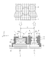
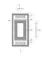
- FIG. 3 is a cross-sectional view showing the structure of the light emitting device 1 of the first embodiment.
- FIG. 3 shows the holder 15 of the light emitting device 1 and the XY cross section of the second housing 43 surrounding the holder 15.
- the light emitting device 1 includes two coils 16 provided in the holder 15 and two magnets 17 provided in the second housing 43 so as to face the coils 16. There is.
- One magnet 17 is arranged in the + X direction of the corresponding coil 16, and the other magnet 17 is arranged in the ⁇ X direction of the corresponding coil 16.
- the arrow Ax shown in FIG. 3 indicates the driving direction of the holder 15.
- the drive direction of the holder 15 of the present embodiment is the ⁇ X direction.
- the coil 16 and the magnet 17 of the present embodiment can drive the holder 15 in the ⁇ X direction by the electromagnetic force acting between the corresponding coil 16 and the magnet 17.
- the collimating lens 13 and the diffractive optical element 14 held by the holder 15 are also driven in the ⁇ X direction.
- the irradiation position of the light emitted from the light source 12 to the subject H moves in the ⁇ X direction.
- the coil 16 and the magnet 17 are examples of the moving portion of the present disclosure, and the collimating lens 13, the diffractive optical element 14, and the holder 15 are examples of predetermined portions driven by the moving portion of the present disclosure.
- the operation of the coil 16 and the magnet 17 may be controlled by a control unit of the light emitting device 1, or may be controlled by a control unit other than the light emitting device 1 (for example, a distance measuring unit 31 of the control device 3).
- the moving portion may be formed by a mechanism different from that of the coil 16 and the magnet 17.
- the moving portion may be realized by piezo drive, and specifically, the holder 15 or the like may be driven by a piezoelectric element (piezo element) that expands and contracts when a voltage is applied.
- the moving portion may be realized by SMA shape memory. Specifically, the shape memory alloy is deformed by changing the ambient temperature of the shape memory alloy by energization to drive the holder 15 and the like. May be good.
- the predetermined portion driven by the moving portion may be an optical system including a collimating lens 13 and / or a diffractive optical element 14, or may be a light source 12 instead of the optical system.
- the light emitting device 1 of the present embodiment includes only two sets of the coil 16 and the magnet 17, and the coil 16 and the magnet 17 are provided only in the ⁇ X direction of the holder 15 among the ⁇ X direction and the ⁇ Y direction of the holder 15. ing. Therefore, the light emitting device 1 of the present embodiment can drive the holder 15 only in the ⁇ X direction out of the ⁇ X direction and the ⁇ Y direction. In other words, the drive of the holder 15 of the present embodiment is not a two-axis drive in the ⁇ X direction and a ⁇ Y direction, but a one-axis drive in the ⁇ X direction. According to the present embodiment, by providing the coil 16 and the magnet 17 only in the ⁇ X direction of the holder 15, it is possible to reduce the size of the light emitting device 1 and the distance measuring system in the Y direction.
- the light emitting device 1 of the present embodiment drives the collimating lens 13, the diffractive optical element 14, and the holder 15 in the ⁇ X direction.
- the light emitting device 1 of the present embodiment may drive only a part of the collimating lens 13, the diffractive optical element 14, and the holder 15 in the ⁇ X direction, or other components of the light emitting device 1 (for example, a light source). 12) may be driven in the ⁇ X direction.
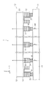
- FIG. 4 is another cross-sectional view showing the structure of the light emitting device 1 of the first embodiment.
- FIG. 4 shows a YZ cross section of the light source driving unit 11 and the light source 12 of the light emitting device 1.
- the light source driving unit 11 is provided inside the substrate 41, and the light source 12 is provided on the surface of the substrate 41.
- the light source 12 includes a substrate 51, a laminated film 52, a plurality of light emitting elements 53, a plurality of anode electrodes 54, and a plurality of cathode electrodes 55.
- the light emitting device 1 further includes a plurality of connection pads 56 provided on the surface of the substrate 41 and a plurality of bumps provided between the anode electrode 54 and the connection pad 56 and between the cathode electrode 55 and the connection pad 56. It is equipped with 57.
- the substrate 51 is a compound semiconductor substrate such as a GaAs (gallium arsenide) substrate.
- FIG. 4 shows the front surface S1 of the substrate 51 facing the ⁇ Z direction and the back surface S2 of the substrate 51 facing the + Z direction.
- the front surface S1 is an example of the first surface of the present disclosure
- the back surface S2 is an example of the second surface of the present disclosure.
- the laminated film 52 includes a plurality of layers laminated on the surface S1 of the substrate 51. Examples of these layers are an n-type semiconductor layer, an active layer, a p-type semiconductor layer, a light reflecting layer, an insulating layer having a light emission window, and the like.
- the laminated film 52 includes a plurality of mesa portions M protruding in the ⁇ Z direction. A part of these mesas portions M is the above-mentioned plurality of light emitting elements 53.
- the light emitting element 53 is provided on the surface S1 of the substrate 51 as a part of the laminated film 52.
- the light emitting element 53 of the present embodiment has a VCSEL structure and emits light in the + Z direction. As shown in FIG. 4, the light emitted from the light emitting element 53 is transmitted from the front surface S1 to the back surface S2 in the substrate 51, and is emitted from the substrate 51 to the collimating lens 13.
- the light source 12 of the present embodiment is a back-illuminated type VCSEL chip.
- the anode electrode 54 is formed at the tip of the light emitting element 53.
- the cathode electrode 55 is formed at the tip of the mesa portion M other than the light emitting element 53, and extends from the tip of the mesa portion M to the surface of the laminated film 52 between the mesa portions M.
- Each light emitting element 53 emits light by flowing a current between the corresponding anode electrode 54 and the corresponding cathode electrode 55.
- the light source 12 is arranged on the surface of the substrate 41 via a bump 57 and a connection pad 56, and is electrically connected to the light source drive unit 11 by the bump 57 and the connection pad 56.
- the connection pad 56 is made of, for example, copper (Cu).
- the bump 57 is made of, for example, gold (Au).
- the light emitting device 1 may include solder instead of the bump 57.
- FIG. 4 schematically shows one or more switch SWs included in the light source driving unit 11. These switch SWs are electrically connected to the corresponding light emitting element 53 via the bump 57.
- the light source driving unit 11 of the present embodiment can drive (on / off) the plurality of light emitting elements 53 by controlling (on / off) these switch SWs. It should be noted that these switch SWs may or may not have a one-to-one correspondence with the light emitting element 53, or may not have a one-to-one correspondence with the light emitting element 53.
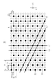
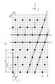
- FIG. 5 is a plan view showing an arrangement example of the light emitting element 53 of the first embodiment.
- FIG. 5 shows a plurality of light emitting elements 53 arranged in a two-dimensional array on the surface S1 of the substrate 51.
- these light emitting elements 53 are indicated by black circles, and a plurality of locations 53'in which the light emitting element 53 does not exist are indicated by broken white circles.
- black circles and the white circles all represent the light emitting element 53
- these light emitting elements 53 are arranged in a square lattice having a lattice constant of ⁇ .
- only the black circles represent the light emitting elements 53, and these light emitting elements 53 are arranged in a triangular lattice pattern.
- FIG. 5 illustrates 90 (6 ⁇ 8 + 6 ⁇ 7) light emitting elements 53.
- the light emitting element 53 of the present embodiment is arranged at each intersection of a plurality of first straight lines L1 extending in the Y direction and a plurality of second straight lines L2 extending in directions non-parallel to the X direction and the Y direction.
- the light emitting elements 53 of the present embodiment are arranged in a parallelogram grid.
- the above-mentioned triangular lattice is obtained by dividing each parallelogram into two.
- the direction in which the second straight line L2 extends is an example of the third direction of the present disclosure.
- FIG. 5 shows two first straight lines L1 adjacent to each other among the plurality of first straight lines L1 and two second straight lines L2 adjacent to each other among the plurality of second straight lines L2. , Shown by a solid line. These two first straight lines L1 extend in the Y direction and are adjacent to each other in the X direction. These two first straight lines L1 are examples of the straight lines A and B of the present disclosure.
- the light emitting elements 53 on the first straight line of these two light emitting elements 53 are arranged so that the light emitting elements 53 are not adjacent to each other in the X direction.
- the eight light emitting elements 53 (black circles) on the first straight line L1 on the left side are adjacent to the eight white circles on the first straight line L1 on the right side in the X direction.
- the eight light emitting elements 53 (black circles) on the first straight line L1 on the right side are adjacent to the eight white circles on the first straight line L1 on the left side in the X direction, respectively. Therefore, on these two first straight lines L1, none of the 16 light emitting elements 53 are adjacent to the other light emitting elements 53 in the X direction. This also applies to the first straight line L1 other than the two first straight lines L1 shown by the solid line.
- the light emitting elements 53 on the first straight line L1 of the present embodiment are not continuously arranged in the Y direction.
- FIG. 5 further shows a plurality of regions R on the surface S1 of the substrate 51. Each of these regions R indicates a region per one light emitting element 53. Each region R is a square having a side length of 2 ⁇ ⁇ .
- FIG. 5 further shows "a / 2", which is the minimum pitch in the X direction between the light emitting elements 53 provided on the surface S1 of the substrate 51, and the Y direction between the light emitting elements 53 provided on the surface S1 of the substrate 51.
- the light emitting device 1 of the present embodiment alternately repeats the generation of light from these light emitting elements 53 and the driving of the holder 15, so that the light is sequentially sent to all the ranging points P in FIG. Can be irradiated to.
- the light emitting device 1 of the present embodiment may execute the operation of driving the holder 15 in the + X direction 22-1 times, that is, 3 times. This makes it possible to change the light irradiation position in the same manner as when the light emitting element 53 is moved as shown by the arrow S in FIG.
- the arrow S shown in FIG. 5 indicates that the operation of moving the light emitting element 53 in the + X direction by ⁇ is executed three times.
- the light emitting element 53 of the present embodiment may be arranged so that each region R is a square having a side length of N ⁇ ⁇ (where N is an integer of 2 or more).
- N an integer of 2 or more
- the pitch a between the light emitting elements 53 adjacent to each other in the X direction is N 2 ⁇ ⁇ .
- A N 2 ⁇ ⁇
- the minimum pitch in the X direction between the light emitting elements 53 is N ⁇ ⁇
- the minimum pitch in the Y direction between the light emitting elements 53 is ⁇ .
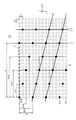
- FIG. 6 is a plan view showing another arrangement example of the light emitting element 53 of the first embodiment.
- FIG. 6 illustrates 40 (8 ⁇ 5) light emitting elements 53.
- each region R is a square having a side length of 3 ⁇ ⁇ .
- the light emitting device 1 of the present embodiment alternately repeats the generation of light from these light emitting elements 53 and the driving of the holder 15, so that the light is sequentially sent to all the ranging points P in FIG. Can be irradiated to.
- the light emitting device 1 of the present embodiment may execute the operation of driving the holder 15 in the + X direction 32-1 times, that is, 8 times. This makes it possible to change the light irradiation position in the same manner as when the light emitting element 53 is moved as shown by the arrow S in FIG.
- the arrow S shown in FIG. 6 indicates that the operation of moving the light emitting element 53 in the + X direction by ⁇ is executed eight times.
- FIG. 7 is a plan view showing another arrangement example of the light emitting element 53 of the first embodiment.
- FIG. 7 illustrates 23 (5 ⁇ 4 + 1 ⁇ 3) light emitting elements 53.
- each region R is a square having a side length of 4 ⁇ ⁇ .
- the light emitting device 1 of the present embodiment alternately repeats the generation of light from these light emitting elements 53 and the driving of the holder 15, so that the light is sequentially sent to all the ranging points P in FIG. Can be irradiated to.
- the light emitting device 1 of the present embodiment may execute the operation of driving the holder 15 in the + X direction 42-1 times, that is, 15 times. This makes it possible to change the light irradiation position in the same manner as when the light emitting element 53 is moved as shown by the arrow S in FIG. 7.
- the arrow S shown in FIG. 7 indicates that the operation of moving the light emitting element 53 in the + X direction by ⁇ is executed 15 times.
- each region R is a square having a side length of N ⁇ ⁇
- the operation of driving the holder 15 in the + X direction is, for example, N2 . -Executed once.
- the value of N in this embodiment may be set to any number.
- Setting a large value of N has an advantage that, for example, the number of light emitting elements 53 can be reduced. By reducing the number of light emitting elements 53, for example, the light source 12 can be miniaturized.
- setting a large value of N has an advantage that, for example, the number of times the holder 15 is driven can be reduced. By reducing the number of times the holder 15 is driven, it is possible to shorten the time required for distance measurement, for example.
- the light emitting element 53 of the present embodiment is arranged at a position other than the intersection of the plurality of first straight lines L1 extending in the Y direction and the plurality of second straight lines L2 extending in the directions non-parallel to the X direction and the Y direction. You may.
- the light emitting element 53 of the present embodiment is arranged at individual intersections of a plurality of first curves having the same shape and a plurality of second curves having the same shape different from the shape of the first curve. May be good. This makes it possible to realize, for example, a pitch relationship similar to the individual pitches shown in FIGS. 5, 6, and 7.
- the density of the light emitting element 53 on the surface S1 of the substrate 51 may be uniform or non-uniform, but it is desirable that the density is uniform.
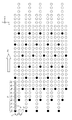
- FIG. 8 is a plan view for explaining an operation example of the light emitting element 53 shown in FIG.
- FIG. 8 shows a plurality of distance measuring points P for measuring the distance to the subject H by using the light emitting element 53 shown in FIG.
- the operation of emitting light from the light emitting element 53 is executed four times, and the operation of driving the holder 15 in the + X direction is executed three times alternately with the operation of emitting light from the light emitting element 53.
- the range-finding points P shown in FIG. 8 include range-finding points Pa to Pd to which light is irradiated by the first to fourth light emission.
- the range-finding points Pa are indicated by black circles
- the range-finding points Pb to Pd are indicated by solid white circles.
- the layout of the AF point Pa shown in FIG. 8 is the same as the layout of the light emitting element 53 shown in FIG. This also applies to the layout of the AF points Pb to Pd.
- FIG. 8 further shows an example of the location P'where the AF point P does not exist, as a white circle with a broken line.
- the arrow C shown in FIG. 8 indicates that one white circle with a broken line exists between the AF points Pa adjacent to each other in the Y direction.
- the light emitting device 1 of the present embodiment alternately repeats the generation of light from the light emitting element 53 and the driving of the holder 15, and as shown by the arrow S, all the ranging points Pa to Pd shown in FIG. Can be irradiated with light in order.
- the AF points Pa to Pd exist on the same XY plane, according to the present embodiment, it is possible to realize the square grid-shaped AF points Pa to Pd as shown in FIG.
- the number of AF points Pa to Pd shown in FIG. 8 is 360 (90 ⁇ 4).
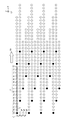
- FIG. 9 is a plan view for explaining an operation example of the light emitting element 53 shown in FIG.
- FIG. 9 shows a plurality of distance measuring points P for measuring the distance to the subject H by using the light emitting element 53 shown in FIG.
- the operation of emitting light from the light emitting element 53 is executed 9 times, and the operation of driving the holder 15 in the + X direction is executed 8 times alternately with the operation of emitting light from the light emitting element 53.
- the range-finding points P shown in FIG. 9 include range-finding points Pa to Pi to which light is irradiated by the first to ninth light emission.
- the AF points Pa are indicated by black circles
- the AF points Pb to Pi are indicated by solid white circles.
- the layout of the AF point Pa shown in FIG. 9 is the same as the layout of the light emitting element 53 shown in FIG. This also applies to the layout of the AF points Pb to Pi.
- FIG. 9 further shows an example of the location P'where the AF point P does not exist, as a white circle with a broken line.
- the arrow C shown in FIG. 9 indicates that two white circles with broken lines exist between the AF points Pa adjacent to each other in the Y direction.
- the light emitting device 1 of the present embodiment alternately repeats the generation of light from the light emitting element 53 and the driving of the holder 15, and as shown by the arrow S, all the ranging points Pa to Pi shown in FIG. Can be irradiated with light in order.
- the AF points Pa to Pi exist on the same XY plane, according to the present embodiment, it is possible to realize the square grid-shaped AF points Pa to Pi as shown in FIG.
- the number of AF points Pa to Pi shown in FIG. 9 is 360 (40 ⁇ 9).
- FIG. 10 is a plan view for explaining an operation example of the light emitting element 53 shown in FIG. 7.
- FIG. 10 shows a plurality of distance measuring points P for measuring the distance to the subject H by using the light emitting element 53 shown in FIG. 7.
- the operation of emitting light from the light emitting element 53 is executed 16 times, and the operation of driving the holder 15 in the + X direction is executed 15 times alternately with the operation of emitting light from the light emitting element 53.
- the range-finding points P shown in FIG. 10 include range-finding points Pa to Pp to which light is irradiated by the first to 16th emission.
- the range-finding points Pa are indicated by black circles
- the range-finding points Pb to Pp are indicated by solid white circles.
- the layout of the AF point Pa shown in FIG. 10 is the same as the layout of the light emitting element 53 shown in FIG. 7. This also applies to the layout of the AF points Pb to Pp.
- FIG. 10 further shows an example of the location P'where the AF point P does not exist, as a white circle with a broken line.
- the arrow C shown in FIG. 10 indicates that three broken white circles exist between the AF points Pa adjacent to each other in the Y direction.
- the light emitting device 1 of the present embodiment alternately repeats the generation of light from the light emitting element 53 and the driving of the holder 15, and as shown by the arrow S, all the ranging points Pa to Pp shown in FIG. Can be irradiated with light in order.
- the AF points Pa to Pp are present on the same XY plane, according to the present embodiment, it is possible to realize the square grid-shaped AF points Pa to Pp as shown in FIG.
- the number of AF points Pa to Pp shown in FIG. 10 is 368 (23 ⁇ 16).
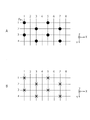
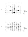
- 11 to 14 are plan views for explaining in detail an operation example of the light emitting element 53 shown in FIG.
- a in FIG. 11 shows a distance measuring point Pa to which light is irradiated by the first light emission.
- FIG. 11B the portion irradiated with the light by the first light emission is indicated by X.
- the layout of X shown in B of FIG. 11 is the same as the layout of the AF point Pa shown in A of FIG.
- a in FIG. 12 shows a ranging point Pb to which light is irradiated by the second light emission.
- the arrow shown by A in FIG. 12 indicates that the portion irradiated with light moves to the AF point Pb.
- B indicates a portion irradiated with light by the first and second light emission by X.
- the number of Xs shown in B of FIG. 12 is twice the number of Xs shown in B of FIG.
- a in FIG. 13 shows a distance measuring point Pc to which light is irradiated by the third light emission.
- the arrow shown by A in FIG. 13 indicates that the portion irradiated with light moves to the AF point Pc.
- B indicates a portion irradiated with light by the first to third light emission by X.
- the number of Xs shown in B of FIG. 13 is three times the number of Xs shown in B of FIG. 11 including the Xs protruding outside the drawing.
- a in FIG. 14 shows a distance measuring point Pd to which light is irradiated by the fourth light emission.
- the arrow shown by A in FIG. 14 indicates that the portion irradiated with light moves to the AF point Pd.
- B indicates a portion irradiated with light by the first to fourth light emission by X.
- the number of Xs shown in FIG. 14B is four times the number of Xs shown in FIG. 11B, including the Xs protruding outside the drawing.
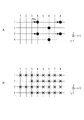
- 15 and 16 are plan views for explaining another operation example of the light emitting element 53 shown in FIG.
- FIG. 15 shows a distance measuring point Pa to which light is irradiated by the first light emission.
- FIG. 15B shows a AF point Pc to which light is irradiated by the second light emission.
- the arrow S shown in FIG. 15B shows how the portion irradiated with light moves from the AF point Pa to the AF point Pc in the + X direction. This can be achieved by driving the holder 15 in the + X direction.
- a in FIG. 16 shows a distance measuring point Pd to which light is irradiated by the third light emission.
- the arrow S newly shown in A of FIG. 16 shows how the portion irradiated with the light moves from the AF point Pc to the AF point Pd in the + X direction. This can be achieved by driving the holder 15 in the + X direction.
- B in FIG. 16 shows a ranging point Pb to which light is irradiated by the fourth light emission.
- the arrow S newly shown in B of FIG. 16 shows how the portion irradiated with the light moves from the ranging point Pd to the focusing point Pb in the ⁇ X direction. This can be achieved by driving the holder 15 in the ⁇ X direction.
- the same ranging points Pa to Pd as those shown in FIG. 8 can be realized by driving the holder 15 in the ⁇ X direction. It will be possible. According to this example, by ending the light emission with the first and second emission, it is possible to obtain an image having half the resolution as in the case of performing the first to fourth emission. Therefore, according to this example, it is possible to obtain a low-resolution image in a short time. According to this example, by ending the light emission with the first light emission, it is possible to obtain an image having a resolution of 1/4 of that when the first to fourth light emission is performed.
- FIG. 17 is a perspective view for explaining the details of the light emitting device 1 of the first embodiment.
- a of FIG. 17 shows a light emitting device 1 of a comparative example of this embodiment.
- the light emitting device 1 of this comparative example includes four sets of coils 16 and magnets 17 in the ⁇ X direction and ⁇ Y direction of the holder 15. Therefore, the light emitting device 1 of this comparative example can drive the holder 15 in the ⁇ X direction and the ⁇ Y direction as shown by the arrows Ax and Ay.
- the drive of the holder 15 in this comparative example is a two-axis drive in the ⁇ X direction and the ⁇ Y direction.
- a of FIG. 17 further includes a distance D between the central axis of the light emitting device 1 and the central axis of the light receiving device 2 (this is referred to as a baseline length) and a space K1 provided in the ⁇ Y direction of the light emitting device 1.
- the space K2 provided in the + Y direction of the light emitting device 1 is shown.
- the distance D in this comparative example includes a length D1 required for arranging the light emitting device 1 and the light receiving device 2, and a length D2 required for securing the spaces K1 and K2.
- the light emitting device 1 of the present embodiment includes two sets of coils 16 and a magnet 17 only in the ⁇ X direction of the holder 15. Therefore, the light emitting device 1 of the present embodiment can drive the holder 15 only in the ⁇ X direction as shown by the arrow Ax. In other words, the drive of the holder 15 of the present embodiment is a uniaxial drive in the ⁇ X direction.
- the distance D of the present embodiment includes the length D1 required for arranging the light emitting device 1 and the light receiving device 2, but does not include the length D2 required for securing the spaces K1 and K2.
- the manufacturing cost of the light emitting device 1 it is possible to reduce the manufacturing cost of the light emitting device 1 (distance measuring system) by downsizing the light emitting device 1 (distance measuring system) and reducing the number of parts. Further, according to the present embodiment, by shortening the baseline length, it is possible to realize a light emitting device 1 (distance measuring system) suitable for distance measurement at a short distance.
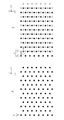
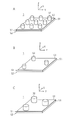
- FIG. 18 is another perspective view for explaining the details of the light emitting device 1 of the first embodiment.
- FIG. 18A shows the substrate 51, the laminated film 52, and the light emitting element 53 of the light emitting device 1 of the comparative example of this embodiment.
- the light emitting device 1 is shown with the front surface S1 of the substrate 51 facing the + Z direction and the back surface S2 of the substrate 51 facing the ⁇ Z direction. This also applies to B and C in FIG. 18 described later.
- the light emitting device 1 of this comparative example does not include the coil 16 and the magnet 17. Therefore, the light emitting device 1 of this comparative example is provided with the light emitting element 53 at high density on the surface S1 of the substrate 51.
- FIG. 18B shows the substrate 51, the laminated film 52, and the light emitting element 53 of the light emitting device 1 of the present embodiment.
- the light emitting device 1 of the present embodiment includes two sets of coils 16 and a magnet 17 in the ⁇ X direction of the holder 15. Therefore, according to the present embodiment, it is possible to irradiate many AF points P with light with a small number of light emitting elements 53. Therefore, the light emitting device 1 shown in FIG. 18B is provided with a light emitting element 53 at a low density on the surface S1 of the substrate 51.
- C in FIG. 18 also shows the substrate 51, the laminated film 52, and the light emitting element 53 of the light emitting device 1 of the present embodiment.
- the light emitting element 53 can be arranged at a low density on the surface S1 of the substrate 51. Therefore, as shown in C of FIG. 18, the size of each light emitting element 53 may be larger than the size of each light emitting element 53 shown in FIGS. A and B. As a result, a large current can be passed through each light emitting element 53, and the distance that can be measured by the distance measuring system can be lengthened.
- connection between the anode electrode 54 and the connection pad 56 and the connection between the cathode electrode 55 and the connection pad 56 can be easily performed by soldering instead of the bump 57, these connections can be made. The cost can be reduced by using solder.
- the light emitting element 53 of the present embodiment is arranged at the intersection of the plurality of first straight lines L1 extending in the Y direction and the plurality of second straight lines L2 extending in the directions non-parallel to the X direction and the Y direction. ing. Further, the light emitting elements 53 on the first straight line L1 adjacent to each other in the X direction are arranged so that the light emitting elements 53 are not adjacent to each other in the X direction. Therefore, according to the present embodiment, it is possible to move the light irradiation position by a suitable method, for example, the light irradiation position can be moved to various places by uniaxial driving.
- the light emitting device 1 of the present embodiment is used as a light source of the distance measuring system, it may be used in other embodiments.
- the light emitting device 1 of the present embodiment may be used as a light source for an optical device such as a printer, or may be used as a lighting device.
- the ranging system of the present embodiment may be used for any purpose, and may be used for biometric authentication such as face recognition and gesture recognition.
- a moving portion for moving the irradiation position of the light by driving a predetermined portion related to the light in the first direction is provided.
- the light emitting element is arranged at an intersection of a plurality of first straight lines extending in a second direction perpendicular to the first direction and a plurality of second straight lines extending in a third direction non-parallel to the first and second directions.
- the first straight line includes a straight line A, the straight line A, and a straight line B adjacent to the first direction.
- the light emitting element on the straight line A and the light emitting element on the straight line B are arranged so as not to be adjacent to each other in the first direction. Light emitting device.
- optical system includes at least one of a lens and an optical diffraction element through which the light from the light emitting element is transmitted.
- the moving portion includes a coil, a magnet, a piezoelectric element, or a shape memory alloy.
- the light emitting element is provided on the first surface of the substrate, and the light emitting element is provided on the first surface of the substrate.
- the minimum pitch in the second direction between the light emitting elements is ⁇
- the minimum pitch in the first direction between the light emitting elements is N ⁇ ⁇ (where N is an integer of 2 or more) (1).
- the region per one light emitting element is given by a square having a side length of N ⁇ ⁇ (where N is an integer of 2 or more). , (1).
- a light emitting device that irradiates the subject with light A light receiving device that receives light reflected from the subject, and a light receiving device.
- a distance measuring device for measuring the distance to the subject based on the light received by the light receiving device is provided.
- the light emitting device is With the plurality of light emitting elements that generate the light, A moving portion for moving the irradiation position of the light by driving a predetermined portion related to the light in the first direction is provided.
- the light emitting element is arranged at an intersection of a plurality of first straight lines extending in a second direction perpendicular to the first direction and a plurality of second straight lines extending in a third direction non-parallel to the first and second directions.
- the first straight line includes a straight line A, the straight line A, and a straight line B adjacent to the first direction.
- the light emitting element on the straight line A and the light emitting element on the straight line B are arranged so as not to be adjacent to each other in the first direction. Distance measurement system.
- the moving unit performs the operation of driving the predetermined portion in the first direction and the operation of driving the predetermined portion in the opposite direction of the first direction N2-1 times, thereby performing the light.
- a moving portion for moving the irradiation position of the light by driving a predetermined portion related to the light in the first direction is provided.
- the minimum pitch in the second direction perpendicular to the first direction between the light emitting elements is ⁇
- the pitch in the first direction between the light emitting elements adjacent to each other in the first direction is N 2 ⁇ ⁇ (.
- N is an integer of 2 or more)
- the pitch in the second direction between the light emitting elements adjacent to each other in the second direction is N ⁇ ⁇ .
Landscapes
- Physics & Mathematics (AREA)
- Engineering & Computer Science (AREA)
- General Physics & Mathematics (AREA)
- Radar, Positioning & Navigation (AREA)
- Remote Sensing (AREA)
- Computer Networks & Wireless Communication (AREA)
- Electromagnetism (AREA)
- Condensed Matter Physics & Semiconductors (AREA)
- Optics & Photonics (AREA)
- Measurement Of Optical Distance (AREA)
Priority Applications (5)
| Application Number | Priority Date | Filing Date | Title |
|---|---|---|---|
| US18/248,741 US20230384424A1 (en) | 2020-10-21 | 2021-09-29 | Light emitting device and ranging system |
| JP2022557346A JPWO2022085381A1 (cg-RX-API-DMAC7.html) | 2020-10-21 | 2021-09-29 | |
| CN202180051893.0A CN116097060A (zh) | 2020-10-21 | 2021-09-29 | 发光装置和测距系统 |
| EP21882522.2A EP4235095A4 (en) | 2020-10-21 | 2021-09-29 | LIGHT-EMITTING DEVICE AND TELEMETRY SYSTEM |
| KR1020237011620A KR20230091869A (ko) | 2020-10-21 | 2021-09-29 | 발광 장치 및 측거 시스템 |
Applications Claiming Priority (2)
| Application Number | Priority Date | Filing Date | Title |
|---|---|---|---|
| JP2020-176730 | 2020-10-21 | ||
| JP2020176730 | 2020-10-21 |
Publications (1)
| Publication Number | Publication Date |
|---|---|
| WO2022085381A1 true WO2022085381A1 (ja) | 2022-04-28 |
Family
ID=81291260
Family Applications (1)
| Application Number | Title | Priority Date | Filing Date |
|---|---|---|---|
| PCT/JP2021/035802 Ceased WO2022085381A1 (ja) | 2020-10-21 | 2021-09-29 | 発光装置および測距システム |
Country Status (7)
| Country | Link |
|---|---|
| US (1) | US20230384424A1 (cg-RX-API-DMAC7.html) |
| EP (1) | EP4235095A4 (cg-RX-API-DMAC7.html) |
| JP (1) | JPWO2022085381A1 (cg-RX-API-DMAC7.html) |
| KR (1) | KR20230091869A (cg-RX-API-DMAC7.html) |
| CN (1) | CN116097060A (cg-RX-API-DMAC7.html) |
| TW (1) | TW202219545A (cg-RX-API-DMAC7.html) |
| WO (1) | WO2022085381A1 (cg-RX-API-DMAC7.html) |
Families Citing this family (1)
| Publication number | Priority date | Publication date | Assignee | Title |
|---|---|---|---|---|
| JP2023183315A (ja) * | 2022-06-15 | 2023-12-27 | 富士フイルムビジネスイノベーション株式会社 | 発光装置、光測距装置、及び、画像形成装置 |
Citations (10)
| Publication number | Priority date | Publication date | Assignee | Title |
|---|---|---|---|---|
| JPH07111559A (ja) * | 1993-10-13 | 1995-04-25 | Dainippon Screen Mfg Co Ltd | 画像露光装置および画像露光方法 |
| JP2007293016A (ja) * | 2006-04-25 | 2007-11-08 | Ricoh Co Ltd | 面発光レーザアレイ、画像形成方法、光走査装置及び画像形成装置 |
| JP2008294010A (ja) * | 2007-05-22 | 2008-12-04 | Ricoh Co Ltd | 面発光レーザアレイ、光走査装置及び画像形成装置 |
| JP2015132600A (ja) * | 2014-01-13 | 2015-07-23 | ジック アーゲー | 光電センサ及び監視領域内の物体の検出方法 |
| US20180062345A1 (en) * | 2016-08-30 | 2018-03-01 | Apple Inc. | Radiation source with a small-angle scanning array |
| JP2019516101A (ja) * | 2016-04-22 | 2019-06-13 | オプシス テック リミテッド | 多波長lidarシステム |
| US20190187255A1 (en) | 2016-09-02 | 2019-06-20 | Lg Innotek Co., Ltd. | Light output module and lidar |
| JP2019159067A (ja) * | 2018-03-12 | 2019-09-19 | 株式会社リコー | 光学装置、これを用いた距離計測装置、及び移動体 |
| WO2020030916A1 (en) | 2018-08-07 | 2020-02-13 | Cambridge Mechatronics Limited | Improved 3d sensing |
| JP2020153796A (ja) * | 2019-03-19 | 2020-09-24 | 株式会社リコー | 測距装置、及び測距方法 |
Family Cites Families (3)
| Publication number | Priority date | Publication date | Assignee | Title |
|---|---|---|---|---|
| KR102184042B1 (ko) | 2014-01-29 | 2020-11-27 | 엘지이노텍 주식회사 | 카메라 장치 |
| US10503265B2 (en) | 2015-09-08 | 2019-12-10 | Microvision, Inc. | Mixed-mode depth detection |
| CN111670383A (zh) * | 2019-01-07 | 2020-09-15 | 深圳市大疆创新科技有限公司 | 一种测距装置及移动平台 |
-
2021
- 2021-09-29 JP JP2022557346A patent/JPWO2022085381A1/ja active Pending
- 2021-09-29 EP EP21882522.2A patent/EP4235095A4/en active Pending
- 2021-09-29 KR KR1020237011620A patent/KR20230091869A/ko active Pending
- 2021-09-29 WO PCT/JP2021/035802 patent/WO2022085381A1/ja not_active Ceased
- 2021-09-29 US US18/248,741 patent/US20230384424A1/en active Pending
- 2021-09-29 CN CN202180051893.0A patent/CN116097060A/zh active Pending
- 2021-10-14 TW TW110138160A patent/TW202219545A/zh unknown
Patent Citations (10)
| Publication number | Priority date | Publication date | Assignee | Title |
|---|---|---|---|---|
| JPH07111559A (ja) * | 1993-10-13 | 1995-04-25 | Dainippon Screen Mfg Co Ltd | 画像露光装置および画像露光方法 |
| JP2007293016A (ja) * | 2006-04-25 | 2007-11-08 | Ricoh Co Ltd | 面発光レーザアレイ、画像形成方法、光走査装置及び画像形成装置 |
| JP2008294010A (ja) * | 2007-05-22 | 2008-12-04 | Ricoh Co Ltd | 面発光レーザアレイ、光走査装置及び画像形成装置 |
| JP2015132600A (ja) * | 2014-01-13 | 2015-07-23 | ジック アーゲー | 光電センサ及び監視領域内の物体の検出方法 |
| JP2019516101A (ja) * | 2016-04-22 | 2019-06-13 | オプシス テック リミテッド | 多波長lidarシステム |
| US20180062345A1 (en) * | 2016-08-30 | 2018-03-01 | Apple Inc. | Radiation source with a small-angle scanning array |
| US20190187255A1 (en) | 2016-09-02 | 2019-06-20 | Lg Innotek Co., Ltd. | Light output module and lidar |
| JP2019159067A (ja) * | 2018-03-12 | 2019-09-19 | 株式会社リコー | 光学装置、これを用いた距離計測装置、及び移動体 |
| WO2020030916A1 (en) | 2018-08-07 | 2020-02-13 | Cambridge Mechatronics Limited | Improved 3d sensing |
| JP2020153796A (ja) * | 2019-03-19 | 2020-09-24 | 株式会社リコー | 測距装置、及び測距方法 |
Non-Patent Citations (1)
| Title |
|---|
| See also references of EP4235095A4 |
Also Published As
| Publication number | Publication date |
|---|---|
| EP4235095A1 (en) | 2023-08-30 |
| JPWO2022085381A1 (cg-RX-API-DMAC7.html) | 2022-04-28 |
| CN116097060A (zh) | 2023-05-09 |
| KR20230091869A (ko) | 2023-06-23 |
| US20230384424A1 (en) | 2023-11-30 |
| TW202219545A (zh) | 2022-05-16 |
| EP4235095A4 (en) | 2024-04-17 |
Similar Documents
| Publication | Publication Date | Title |
|---|---|---|
| US11320666B2 (en) | Integrated structured-light projector | |
| US11852463B2 (en) | Projectors of structured light | |
| US9553423B2 (en) | Miniature structured light illuminator | |
| US9825425B2 (en) | Integrated structured-light projector comprising light-emitting elements on a substrate | |
| US10353215B2 (en) | Generation of coded structured light patterns using VCSEL arrays | |
| CN104360571B (zh) | 光学设备和成像系统 | |
| US10506148B2 (en) | Integrated photonics module for optical projection | |
| CN208940077U (zh) | 红外相机模块及其图像传感器以及电子装置 | |
| US12566266B2 (en) | Lighting device and distance measurement apparatus | |
| US10122146B2 (en) | Thin laser package for optical applications | |
| WO2021024508A1 (ja) | 発光装置、光学装置及び情報処理装置 | |
| WO2021235162A1 (ja) | 発光装置および測距装置 | |
| CN116438480A (zh) | 光检测装置 | |
| US20240310489A1 (en) | Illumination device and distance measuring device | |
| US20230384424A1 (en) | Light emitting device and ranging system | |
| TW202300948A (zh) | 用於三維測距系統的點陣投影器 | |
| CN220171253U (zh) | 一种3d模组及电子设备 | |
| US20230266465A1 (en) | Distance measuring camera | |
| KR20230146196A (ko) | 복수의 광원을 포함한 광 모듈 | |
| JP2023068209A (ja) | 測距装置および発光装置 | |
| KR20220000599A (ko) | 카메라 모듈 |
Legal Events
| Date | Code | Title | Description |
|---|---|---|---|
| 121 | Ep: the epo has been informed by wipo that ep was designated in this application |
Ref document number: 21882522 Country of ref document: EP Kind code of ref document: A1 |
|
| ENP | Entry into the national phase |
Ref document number: 2022557346 Country of ref document: JP Kind code of ref document: A |
|
| NENP | Non-entry into the national phase |
Ref country code: DE |
|
| ENP | Entry into the national phase |
Ref document number: 2021882522 Country of ref document: EP Effective date: 20230522 |