WO2022083205A1 - 一种电子设备及其供电单元 - Google Patents
一种电子设备及其供电单元 Download PDFInfo
- Publication number
- WO2022083205A1 WO2022083205A1 PCT/CN2021/109186 CN2021109186W WO2022083205A1 WO 2022083205 A1 WO2022083205 A1 WO 2022083205A1 CN 2021109186 W CN2021109186 W CN 2021109186W WO 2022083205 A1 WO2022083205 A1 WO 2022083205A1
- Authority
- WO
- WIPO (PCT)
- Prior art keywords
- bridge resonant
- power supply
- supply unit
- balance coils
- input
- Prior art date
- Legal status (The legal status is an assumption and is not a legal conclusion. Google has not performed a legal analysis and makes no representation as to the accuracy of the status listed.)
- Ceased
Links
Images




Classifications
-
- H—ELECTRICITY
- H02—GENERATION; CONVERSION OR DISTRIBUTION OF ELECTRIC POWER
- H02J—ELECTRIC POWER NETWORKS; CIRCUIT ARRANGEMENTS OR SYSTEMS FOR SUPPLYING OR DISTRIBUTING ELECTRIC POWER; SYSTEMS FOR STORING ELECTRIC ENERGY
- H02J1/00—Circuit arrangements for DC mains or DC distribution networks
- H02J1/10—Parallel operation of DC sources
- H02J1/102—Parallel operation of DC sources being switching converters
-
- H—ELECTRICITY
- H02—GENERATION; CONVERSION OR DISTRIBUTION OF ELECTRIC POWER
- H02M—APPARATUS FOR CONVERSION BETWEEN AC AND AC, BETWEEN AC AND DC, OR BETWEEN DC AND DC, AND FOR USE WITH MAINS OR SIMILAR POWER SUPPLY SYSTEMS; CONVERSION OF DC OR AC INPUT POWER INTO SURGE OUTPUT POWER; CONTROL OR REGULATION THEREOF
- H02M7/00—Conversion of AC power input into DC power output; Conversion of DC power input into AC power output
- H02M7/02—Conversion of AC power input into DC power output without possibility of reversal
- H02M7/04—Conversion of AC power input into DC power output without possibility of reversal by static converters
- H02M7/12—Conversion of AC power input into DC power output without possibility of reversal by static converters using discharge tubes with control electrode or semiconductor devices with control electrode
- H02M7/21—Conversion of AC power input into DC power output without possibility of reversal by static converters using discharge tubes with control electrode or semiconductor devices with control electrode using devices of a triode or transistor type requiring continuous application of a control signal
- H02M7/217—Conversion of AC power input into DC power output without possibility of reversal by static converters using discharge tubes with control electrode or semiconductor devices with control electrode using devices of a triode or transistor type requiring continuous application of a control signal using semiconductor devices only
- H02M7/25—Conversion of AC power input into DC power output without possibility of reversal by static converters using discharge tubes with control electrode or semiconductor devices with control electrode using devices of a triode or transistor type requiring continuous application of a control signal using semiconductor devices only arranged for operation in series, e.g. for multiplication of voltage
-
- Y—GENERAL TAGGING OF NEW TECHNOLOGICAL DEVELOPMENTS; GENERAL TAGGING OF CROSS-SECTIONAL TECHNOLOGIES SPANNING OVER SEVERAL SECTIONS OF THE IPC; TECHNICAL SUBJECTS COVERED BY FORMER USPC CROSS-REFERENCE ART COLLECTIONS [XRACs] AND DIGESTS
- Y02—TECHNOLOGIES OR APPLICATIONS FOR MITIGATION OR ADAPTATION AGAINST CLIMATE CHANGE
- Y02B—CLIMATE CHANGE MITIGATION TECHNOLOGIES RELATED TO BUILDINGS, e.g. HOUSING, HOUSE APPLIANCES OR RELATED END-USER APPLICATIONS
- Y02B70/00—Technologies for an efficient end-user side electric power management and consumption
- Y02B70/10—Technologies improving the efficiency by using switched-mode power supplies [SMPS], i.e. efficient power electronics conversion e.g. power factor correction or reduction of losses in power supplies or efficient standby modes
Definitions
- the invention relates to the technical field of electronic engineering, in particular to an electronic device and a power supply unit thereof.
- the Share bus communicates and adjusts the voltage to control the current sharing.
- the purpose of the present invention is to provide an electronic device and a power supply unit thereof, so as to alleviate (reduce, reduce, etc.) the purpose of achieving current balance through current sharing inductance existing in the prior art as a low-cost, high-efficiency isolation Technical problems with the power supply.
- the present invention provides a power supply unit, comprising two half-bridge resonant topology circuits and two balance coils;
- the input ends of the two half-bridge resonant topology circuits are respectively connected to both ends of the AC input, and the output ends of the two half-bridge resonant topology circuits are respectively connected to both ends of the DC load;
- Two balance coils are wound on the primary side or the secondary side of the two half-bridge resonant topology circuits respectively;
- the number of turns of the two balance coils is equal, and the two balance coils are connected end to end.
- each half-bridge resonant topology circuit also includes a power factor correction circuit connected between each half-bridge resonant topology circuit and the AC input.
- it also includes an electromagnetic interference filter circuit connected between each power factor correction circuit and the AC input.
- the half-bridge resonant topology circuit includes a primary coil and a secondary coil
- One end of the primary coil is connected to the AC input, the other end of the primary coil is grounded, and both ends of the secondary coil are respectively connected to one end of the DC load through diodes.
- the AC input power supply is 220V.
- the present invention also provides an electronic device, including the power supply unit.
- the electronic device is a server.
- an electronic device and a power supply unit thereof provided by an embodiment of the present invention include two half-bridge resonant topology circuits and two balanced coils; the input ends of the two half-bridge resonant topology circuits are respectively connected to two ends of the AC input, The output ends of the two half-bridge resonant topology circuits are connected to the two ends of the DC load respectively; the two balance coils are wound on the primary side or the secondary side of the two half-bridge resonant topology circuits respectively; the turns of the two balance coils are equal, and The two balance coils are connected end to end.
- the two balance coils are respectively wound in the transformer of the half-bridge resonant topology circuit to achieve the function of balancing the current through parallel current sharing, which does not require additional space and does not require complex circuit control.
- Good current equalization effect due to the simple use of passive component characteristics, it is not easy to make mistakes and has good reliability characteristics.
- Fig. 1 is the existing circuit diagram
- Fig. 2 is an existing analog waveform diagram
- FIG. 3 is a schematic diagram of a power supply unit provided by an embodiment of the present invention.
- FIG. 4 is a broken line diagram of voltage according to an embodiment of the present invention.
- FIG. 5 is an AC circuit diagram of an LLC resonant converter provided by an embodiment of the present invention.
- FIG. 6 is a gain curve diagram of an LLC resonant converter provided by an embodiment of the present invention.
- FIG. 8 is a circuit diagram of a power supply unit provided by an embodiment of the present invention.
- FIG. 9 is a partial circuit diagram of the balance coil in FIG. 8 .
- the invention proposes a new method for parallel current sharing of half-bridge resonant LLC topology, which can achieve the purpose of current balance through current sharing inductors as a low-cost, high-efficiency isolated power supply.
- the present invention provides a technical solution, a power supply unit, comprising two half-bridge resonant topology circuits and two balance coils;
- the input ends of the two half-bridge resonant topology circuits are respectively connected to both ends of the AC input, and the output ends of the two half-bridge resonant topology circuits are respectively connected to both ends of the DC load;
- Two balance coils are wound on the primary side or the secondary side of the two half-bridge resonant topology circuits respectively;
- the number of turns of the two balance coils is equal, and the two balance coils are connected end to end.
- the corresponding electronic devices also includes a power factor correction (Power Factor Correction, PFC for short) circuit connected between each half-bridge resonant topology circuit and the AC input.
- Power factor correction refers to improving the power factor and making the power factor close to 1. This is by making the power factor angle (phase angle) close to 0°, thereby reducing the phase difference between the voltage and the current, and making the apparent power close to the effective power.
- harmonic currents are suppressed. Harmonic suppression has been classified in the international standard IEC61000-3-2 and the maximum rated harmonic current has been specified, and the corresponding electronic devices are basically equipped with power factor correction circuits.
- EMI filter circuit is electronic passive components used to suppress signals or power lines with conducted interference.
- Electromagnetic interference is natural or man-made unacceptable electromagnetic radiation that causes degradation or malfunction of electronic equipment.
- EMI filter circuits are devices that can be used to suppress electromagnetic interference, usually consisting of components that suppress differential and common mode interference.
- the half-bridge resonant topology circuit includes a primary coil and a secondary coil;
- One end of the primary coil is connected to the AC input, the other end of the primary coil is grounded, and both ends of the secondary coil are respectively connected to one end of the DC load through diodes.
- the midpoint of the secondary coil of the half-bridge resonant topology circuit is grounded.
- the AC input power supply is 220V.
- the present invention also provides an electronic device, including the power supply unit provided in the above embodiment.
- the electronic device is a server.
- two balanced coils with the same number of turns are added.
- the two balance coils are respectively wound on the primary sides of the two half-bridge resonant topology circuits, and are connected end to end to participate in resonance to form a circuit balance effect.
- the first balance coil N1 and the primary coil of the transformer of the first half-bridge resonant topology circuit are wound together on the same iron core
- the second balance coil N2 and the transformer of the second half-bridge resonant topology circuit are wound on the same iron core.
- the primary coils are wound together on the same iron core, and the upper end 12 port of the first balance coil N1 is connected to the lower end 12 port of the second balance coil N2, and the lower end 11 port of the first balance coil N1 is connected to the second balance coil.
- the 11 ports on the upper end of N2 form end-to-end connections.
- the two balance coils can also be respectively wound on the secondary sides of the two half-bridge resonant topology circuits to form end-to-end connections, which can also participate in resonance to form a circuit balance effect.
- Cr is the resonant capacitor
- Lr is the resonant inductance
- Lm is the inductance
- Np is the number of turns on the primary side
- Ns is the number of turns on the secondary side
- R 0 is the secondary test load
- Ra is the primary test load.
- Different voltages are equivalent to different output loads R 0 , which can be equivalent to the primary side AC load Rac according to the ratio n of the number of turns Np on the primary side to the number of turns Ns on the secondary side.
- transformer current coil ratio The ideal transformer current is inversely proportional to the coil ratio.
- N 1 i 1 N 2 i 2
- the above formula can show that the same number of turns will have the same current.
- the voltage of an ideal transformer is proportional to the number of turns, and the current is inversely proportional to the number of turns.
- the above formula is the relationship between the transformer current and the number of turns, where N 1 is the number of turns on the primary side, and N 2 is the number of turns on the secondary side, i 1 is the primary side current, and i 2 is the secondary side current.
Landscapes
- Engineering & Computer Science (AREA)
- Power Engineering (AREA)
- Dc-Dc Converters (AREA)
Abstract
一种电子设备及其供电单元,属于电子工程的技术领域,该供电单元包括两个半桥谐振拓扑电路和两个平衡线圈;两个半桥谐振拓扑电路的输入端分别连接交流输入的两端,两个半桥谐振拓扑电路的输出端分别连接直流负载的两端;两个平衡线圈分别缠绕在两个半桥谐振拓扑电路的初级侧或次级侧;两个平衡线圈的匝数相等,且两个平衡线圈首尾互相连接。两个平衡线圈分别在半桥谐振拓扑电路的变压器内以绕组的方式,通过并联均流来达到平衡电流的功能,不需要额外占用空间,没有复杂的电路控制,利用基础物理原理即可达到非常好的均流效果,由于单纯使用被动组件特性,因此不易出错,拥有良好可靠度特性的问题。
Description
本申请要求于2020年10月23日提交至中国专利局、申请号为202011143531.8、发明名称为“一种电子设备及其供电单元”的中国专利申请的优先权,其全部内容通过引用结合在本申请中。
本发明涉及电子工程技术领域,尤其是涉及一种电子设备及其供电单元。
随着用户对用电质量需求和高电力密度的要求,电源的并联使用也越来越常见,电源并联首先需要克服的一大难题为电流均流度的实践,传统均流方式大多为透过Share bus沟通调整电压进而控制电流均流度。
此方式往往更为复杂,且对回授介入控制,若无优化调整,轻则电流不均流,严重会造成系统不稳定甚至损坏的风险。
发明内容
本发明的目的在于提供一种电子设备及其供电单元,以缓解了(减少了、降低了等)现有技术中存在的透过均流电感来达到电流平衡目作为低成本、高效率的隔离电源的技术问题。
第一方面,本发明提供的一种供电单元,包括两个半桥谐振拓扑电路和两个平衡线圈;
两个半桥谐振拓扑电路的输入端分别连接交流输入的两端,两个半桥谐振拓扑电路的输出端分别连接直流负载的两端;
两个平衡线圈分别缠绕在两个半桥谐振拓扑电路的初级侧或次级侧;
两个平衡线圈的匝数相等,且两个平衡线圈首尾互相连接。
进一步的,还包括连接于每个半桥谐振拓扑电路与交流输入之间的功率因数校正电路。
进一步的,还包括连接于每个功率因数校正电路与交流输入之间的电磁干扰滤波电路。
进一步的,半桥谐振拓扑电路包括初级线圈和次级线圈;
其中,初级线圈的一端连接交流输入,初级线圈的另一端接地,次级线圈的两端分别通过二极管连接直流负载的一端。
进一步的,半桥谐振拓扑电路的次级线圈的中点接地。
进一步的,交流输入的电源为220V。
第二方面,本发明还提供一种电子设备,包括所述的供电单元。
进一步的,所述电子设备为服务器。
相应地,本发明实施例提供的一种电子设备及其供电单元,包括两个半桥谐振拓扑电路和两个平衡线圈;两个半桥谐振拓扑电路的输入端分别连接交流输入的两端,两个半桥谐振拓扑电路的输出端分别连接直流负载的两端;两个平衡线圈分别缠绕在两个半桥谐振拓扑电路的初级侧或次级侧;两个平衡线圈的匝数相等,且两个平衡线圈首尾互相连接。两个平衡线圈分别在半桥谐振拓扑电路的变压器内以绕组的方式,通过并联均流来达到平衡电流的功能,不需要额外占用空间,没有复杂的电路控制,利用基础物理原理即可达到非常好的均流效果,由于单纯使用被动组件特性,因此不易出错,拥有良好可靠度特性的问题。
为了更清楚地说明本发明具体实施方式或现有技术中的技术方案,下面将对具体实施方式或现有技术描述中所需要使用的附图作简单地介绍,显而易见地,下面描述中的附图是本发明的一些实施方式,对于本领域普通技术人员来讲,在不付出创造性劳动的前提下,还可以根据这些附图获得其他的附图。
图1为现有的电路图;
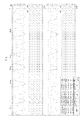
图2为现有的模拟波形图;
图3为本发明实施例提供的供电单元示意图;
图4为本发明实施例的电压折线图;
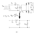
图5为本发明实施例提供的LLC谐振变换器的交流电路图;
图6为本发明实施例提供的LLC谐振变换器的增益曲线图;
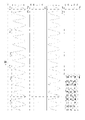
图7为本发明实施例提供的平衡后的模拟波形图;
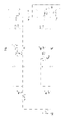
图8为本发明实施例提供的供电单元电路图;
图9为图8中平衡线圈的局部电路图。
为使本发明实施例的目的、技术方案和优点更加清楚,下面将结合附图对本发明的技术方案进行清楚、完整地描述,显然,所描述的实施例是本发明一部分实施例,而不是全部的实施例。基于本发明中的实施例,本领域普通技术人员在没有做出创造性劳动前提下所获得的所有其他实施例,都属于本发明保护的范围。
本发明对半桥谐振LLC拓扑并联均流提出一种新的方法,可以透过均流电感来达到电流平衡目作为低成本、高效率的隔离电源。
本发明提供一种技术方案,一种供电单元,包括两个半桥谐振拓扑电路和两个平衡线圈;
两个半桥谐振拓扑电路的输入端分别连接交流输入的两端,两个半桥谐振拓扑电路的输出端分别连接直流负载的两端;
两个平衡线圈分别缠绕在两个半桥谐振拓扑电路的初级侧或次级侧;
两个平衡线圈的匝数相等,且两个平衡线圈首尾互相连接。
优选的,还包括连接于每个半桥谐振拓扑电路与交流输入之间的功率因数校正(Power Factor Correction,简称PFC)电路。功率因子校正是指改善功率因子,并使功率因子接近1。这是通过使功率因子角(相位角)接近0°,从而减小电压与电流的相位差,使视在功率接近有效功率。同时抑制谐波电流。谐波抑制在国际标准IEC61000-3-2中已经分类限值并规定了最大额定谐波电流,对应的电子装置基本上都配备功率因子校正电路。
优选的,还包括连接于每个功率因数校正电路与交流输入之间的电磁干扰(Electro Magnetic Interference,简称EMI)滤波电路。EMI滤波电路是用于抑制存在传导干扰的信号或电源线的电子被动元器件。电磁干扰是天然或人造的不能接受的电磁辐射,导致电子设备的退化或故障。EMI滤波电路是可以用于抑制电磁干扰的装置,通常由抑制差分和共模干扰的组件组成。
优选的,半桥谐振拓扑电路包括初级线圈和次级线圈;
其中,初级线圈的一端连接交流输入,初级线圈的另一端接地,次级线圈的两端分别通过二极管连接直流负载的一端。
优选的,半桥谐振拓扑电路的次级线圈的中点接地。
优选的,交流输入的电源为220V。
本发明还提供的一种电子设备,包括上述实施例提供的供电单元。
优选的,所述电子设备为服务器。
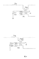
在本实施例中需要说明的是,如图1所示,R11=50m ohm&R12=5m ohm为并联路径所产生的等效阻抗。
如图2所示,若不做任何均流控制,R11=2.2A、R12=7.7A,两组输出电流差异非常大。
如图3、图8和图9所示,本发明实施例加入两个匝数相等的平衡线圈。两个平衡线圈分别缠绕在两个半桥谐振拓扑电路的初级侧,且首尾互相连接,参与谐振形成电路平衡效果。具体的,第一个平衡线圈N1和第一个半桥谐振拓扑电路的变压器的初级线圈共同缠绕在同一个铁芯上,第二个平衡线圈N2和第二个半桥谐振拓扑电路的变压器的初级线圈共同缠绕在同一个铁芯上,而且第一个平衡线圈N1的上端12端口连接第二个平衡线圈N2的下端12端口,第一个平衡线圈N1的下端11端口连接第二个平衡线圈N2的上端11端口,形成首尾互相连接。
在其他实施方式中,两个平衡线圈也可以分别缠绕在两个半桥谐振拓扑电路的次级侧,形成首尾互相连接,同样能够参与谐振形成电路平衡效果。
如图4所示,由于平衡线圈会造成谐振槽改变进而改变放大增益,输出电压V1、V2会分别被改变。
如图5所示,Cr为谐振电容,Lr为谐振电感,Lm为电感,Np为初级侧匝数,Ns为次级侧匝数,R
0为次级测负载,Ra为初级测等校负载。不同的电压等效出不同的输出负载R
0,根据初级侧匝数Np与次级侧匝数Ns的比值n,进而可以等效到初级侧交流负载Rac。
如图6所示,其中,Q为品质因数,可以得知不同的Rac会影响增益曲线,造成两组并联的LLC电压输出不同,进而改变输出电压造成输出电流自然平衡。
如图7所示,可以得出模拟结果,加入平衡线圈可以发现流经输出等效电阻R11=5A、R12=5A,电流输出可以达到均流效果。
另外也可以根据以下算式变压器电流圈比公式说明,理想变压器电流 与圈比为反比关系,透过1:1等比变压器可达到变压器初级侧与次级侧相同电流的结果如下:
N
1i
1=N
2i
2

以上算式可说明相同的匝数会有相同的电流,理想变压器的电压正比于匝数,电流反比于匝数,以上算式是变压器电流与匝数关系,其中N
1为初级侧匝数,N
2为次级侧匝数,i
1为初级侧电流,i
2为次级侧电流。
本发明实施例中所提到的术语“包括”和“具有”以及它们的任何变形,意图在于覆盖不排他的包含。例如包含了一系列步骤或单元的过程、方法、系统、产品或设备没有限定于已列出的步骤或单元,而是可选地还包括其他没有列出的步骤或单元,或可选地还包括对于这些过程、方法、产品或设备固有的其它步骤或单元。
应注意到:相似的标号和字母在下面的附图中表示类似项,因此,一旦某一项在一个附图中被定义,则在随后的附图中不需要对其进行进一步定义和解释。
在本发明的描述中,需要说明的是,术语“中心”、“上”、“下”、“左”、“右”、“竖直”、“水平”、“内”、“外”等指示的方位或位置关系为基于附图所示的方位或位置关系,或者是该发明产品使用时惯常摆放的方位或位置关系,仅是为了便于描述本发明和简化描述,而不是指示或暗示所指的装置或组件必须具有特定的方位、以特定的方位构造和操作,因此不能理解为对本发明的限制。此外,术语“第一”、“第二”、“第三”等仅用于区分描述,而不能理解为指示或暗示相对重要性。
在本发明的描述中,还需要说明的是,除非另有明确的规定和限定,术语“设置”、“安装”、“相连”、“连接”应做广义理解,例如,可以是固定连接,也可以是可拆卸连接,或一体地连接;可以是机械连接,也可以是电连接;可以是直接相连,也可以通过中间媒介间接相连,可以是两个组件内部的连通。对于本领域的普通技术人员而言,可以具体情况理解上述术语在本发明中的具体含义。
Claims (8)
- 一种供电单元,其特征在于,包括两个半桥谐振拓扑电路和两个平衡线圈;两个半桥谐振拓扑电路的输入端分别连接交流输入的两端,两个半桥谐振拓扑电路的输出端分别连接直流负载的两端;两个平衡线圈分别缠绕在两个半桥谐振拓扑电路的初级侧或次级侧;两个平衡线圈的匝数相等,且两个平衡线圈首尾互相连接。
- 根据权利要求1所述的供电单元,其特征在于,还包括连接于每个半桥谐振拓扑电路与交流输入之间的功率因数校正电路。
- 根据权利要求2所述的供电单元,其特征在于,还包括连接于每个功率因数校正电路与交流输入之间的电磁干扰滤波电路。
- 根据权利要求1所述的供电单元,其特征在于,半桥谐振拓扑电路包括初级线圈和次级线圈;其中,初级线圈的一端连接交流输入,初级线圈的另一端接地,次级线圈的两端分别通过二极管连接直流负载的一端。
- 根据权利要求4所述的供电单元,其特征在于,半桥谐振拓扑电路的次级线圈的中点接地。
- 根据权利要求1所述的供电单元,其特征在于,交流输入的电源为220V。
- 一种电子设备,其特征在于,包括如权利要求1至6任一项所述的供电单元。
- 根据权利要求7所述的电子设备,其特征在于,所述电子设备为服务器。
Applications Claiming Priority (2)
| Application Number | Priority Date | Filing Date | Title |
|---|---|---|---|
| CN202011143531.8 | 2020-10-23 | ||
| CN202011143531.8A CN112350299A (zh) | 2020-10-23 | 2020-10-23 | 一种电子设备及其供电单元 |
Publications (1)
| Publication Number | Publication Date |
|---|---|
| WO2022083205A1 true WO2022083205A1 (zh) | 2022-04-28 |
Family
ID=74359867
Family Applications (1)
| Application Number | Title | Priority Date | Filing Date |
|---|---|---|---|
| PCT/CN2021/109186 Ceased WO2022083205A1 (zh) | 2020-10-23 | 2021-07-29 | 一种电子设备及其供电单元 |
Country Status (2)
| Country | Link |
|---|---|
| CN (1) | CN112350299A (zh) |
| WO (1) | WO2022083205A1 (zh) |
Families Citing this family (1)
| Publication number | Priority date | Publication date | Assignee | Title |
|---|---|---|---|---|
| CN112350299A (zh) * | 2020-10-23 | 2021-02-09 | 苏州浪潮智能科技有限公司 | 一种电子设备及其供电单元 |
Citations (6)
| Publication number | Priority date | Publication date | Assignee | Title |
|---|---|---|---|---|
| US20140153293A1 (en) * | 2012-11-30 | 2014-06-05 | Chung-Shan Institute Of Science And Technology | Double-Output Half-Bridge LLC Serial Resonant Converter |
| US9125259B1 (en) * | 2012-05-03 | 2015-09-01 | Universal Lighting Technologies, Inc. | Constant current drive circuit for multi-channel LED lighting |
| CN204859623U (zh) * | 2015-06-25 | 2015-12-09 | 深圳麦格米特电气股份有限公司 | 一种led多路均流控制电路 |
| CN110588395A (zh) * | 2019-09-09 | 2019-12-20 | 国网山东省电力公司金乡县供电公司 | 一种车载充电机控制电路、方法、充电机及电动汽车 |
| CN210380663U (zh) * | 2019-09-30 | 2020-04-21 | 深圳古瑞瓦特新能源股份有限公司 | 一种双向多路并联全桥llc谐振变换器 |
| CN112350299A (zh) * | 2020-10-23 | 2021-02-09 | 苏州浪潮智能科技有限公司 | 一种电子设备及其供电单元 |
Family Cites Families (1)
| Publication number | Priority date | Publication date | Assignee | Title |
|---|---|---|---|---|
| CN101873739B (zh) * | 2009-04-27 | 2014-07-30 | 台达电子工业股份有限公司 | 多组直流负载的电流平衡供电电路 |
-
2020
- 2020-10-23 CN CN202011143531.8A patent/CN112350299A/zh active Pending
-
2021
- 2021-07-29 WO PCT/CN2021/109186 patent/WO2022083205A1/zh not_active Ceased
Patent Citations (6)
| Publication number | Priority date | Publication date | Assignee | Title |
|---|---|---|---|---|
| US9125259B1 (en) * | 2012-05-03 | 2015-09-01 | Universal Lighting Technologies, Inc. | Constant current drive circuit for multi-channel LED lighting |
| US20140153293A1 (en) * | 2012-11-30 | 2014-06-05 | Chung-Shan Institute Of Science And Technology | Double-Output Half-Bridge LLC Serial Resonant Converter |
| CN204859623U (zh) * | 2015-06-25 | 2015-12-09 | 深圳麦格米特电气股份有限公司 | 一种led多路均流控制电路 |
| CN110588395A (zh) * | 2019-09-09 | 2019-12-20 | 国网山东省电力公司金乡县供电公司 | 一种车载充电机控制电路、方法、充电机及电动汽车 |
| CN210380663U (zh) * | 2019-09-30 | 2020-04-21 | 深圳古瑞瓦特新能源股份有限公司 | 一种双向多路并联全桥llc谐振变换器 |
| CN112350299A (zh) * | 2020-10-23 | 2021-02-09 | 苏州浪潮智能科技有限公司 | 一种电子设备及其供电单元 |
Also Published As
| Publication number | Publication date |
|---|---|
| CN112350299A (zh) | 2021-02-09 |
Similar Documents
| Publication | Publication Date | Title |
|---|---|---|
| US11062837B2 (en) | Planar transformer, power conversion circuit, and adapter | |
| CN103081319B (zh) | 共模噪声减少设备和方法 | |
| CN109617250B (zh) | 一种基于组合型拓扑的抗偏移无线电能传输系统 | |
| CN103477544B (zh) | 共模滤波器装置 | |
| CN110310815A (zh) | 平面变压器、电源转换电路以及适配器 | |
| JP4483863B2 (ja) | ノイズ抑制回路 | |
| US12119740B2 (en) | DC/DC converter and communication power supply with common mode noise suppression | |
| CN105958809A (zh) | 带有耦合电感的滤波器及其参数确定方法 | |
| CN111614094B (zh) | 电磁干扰滤波电路 | |
| WO2022083205A1 (zh) | 一种电子设备及其供电单元 | |
| CN108988615B (zh) | 一种并联均流电路拓扑结构 | |
| CN107819397A (zh) | 输入滤波器及其设置方法、包括该输入滤波器的变频器 | |
| He et al. | Common-mode noise reduction in full-bridge LLC resonant converter with split primary winding transformer | |
| CN207504755U (zh) | 输入滤波器及包括该输入滤波器的变频器 | |
| CN205901578U (zh) | 带有耦合电感的滤波器 | |
| CN117895913A (zh) | 一种利用感性补偿模块的电压采样式传导电磁干扰抑制电路 | |
| CN111464009B (zh) | 适于移相控制全桥变换器的共模电压对消方法和装置 | |
| CN117748587A (zh) | 一种多有源桥直流变压器的均衡控制方法及装置 | |
| CN115173757A (zh) | 一种控制器电源输入电路 | |
| CN119853039B (zh) | 光伏储能一体机的滤波器以及光伏储能一体机 | |
| CN118316304B (zh) | 一种基于阻抗平衡的无源emi滤波器及变换器系统 | |
| Yau | Hybrid Power Filter for Differential-Mode and Common-Mode Noise Currents | |
| Osada et al. | Current Balancing Using a Coupled Inductor Pair in Multi-Parallel Megahertz Wireless Power Transfer Systems | |
| CN121966259A (zh) | 电流采样电流补偿的差模有源emi滤波器及系统 | |
| TW202614548A (zh) | 諧振轉換器 |
Legal Events
| Date | Code | Title | Description |
|---|---|---|---|
| 121 | Ep: the epo has been informed by wipo that ep was designated in this application |
Ref document number: 21881625 Country of ref document: EP Kind code of ref document: A1 |
|
| NENP | Non-entry into the national phase |
Ref country code: DE |
|
| 122 | Ep: pct application non-entry in european phase |
Ref document number: 21881625 Country of ref document: EP Kind code of ref document: A1 |