WO2022065201A1 - フィルタ装置およびそれを備える高周波フロントエンド回路 - Google Patents
フィルタ装置およびそれを備える高周波フロントエンド回路 Download PDFInfo
- Publication number
- WO2022065201A1 WO2022065201A1 PCT/JP2021/034149 JP2021034149W WO2022065201A1 WO 2022065201 A1 WO2022065201 A1 WO 2022065201A1 JP 2021034149 W JP2021034149 W JP 2021034149W WO 2022065201 A1 WO2022065201 A1 WO 2022065201A1
- Authority
- WO
- WIPO (PCT)
- Prior art keywords
- flat plate
- plate electrode
- parallel resonator
- filter device
- inductor
- Prior art date
- Legal status (The legal status is an assumption and is not a legal conclusion. Google has not performed a legal analysis and makes no representation as to the accuracy of the status listed.)
- Ceased
Links
Images







Classifications
-
- H—ELECTRICITY
- H03—ELECTRONIC CIRCUITRY
- H03H—IMPEDANCE NETWORKS, e.g. RESONANT CIRCUITS; RESONATORS
- H03H7/00—Multiple-port networks comprising only passive electrical elements as network components
- H03H7/01—Frequency selective two-port networks
- H03H7/0115—Frequency selective two-port networks comprising only inductors and capacitors
-
- H—ELECTRICITY
- H01—ELECTRIC ELEMENTS
- H01F—MAGNETS; INDUCTANCES; TRANSFORMERS; SELECTION OF MATERIALS FOR THEIR MAGNETIC PROPERTIES
- H01F17/00—Fixed inductances of the signal type
- H01F17/0006—Printed inductances
- H01F17/0013—Printed inductances with stacked layers
-
- H—ELECTRICITY
- H01—ELECTRIC ELEMENTS
- H01F—MAGNETS; INDUCTANCES; TRANSFORMERS; SELECTION OF MATERIALS FOR THEIR MAGNETIC PROPERTIES
- H01F27/00—Details of transformers or inductances, in general
- H01F27/28—Coils; Windings; Conductive connections
- H01F27/2804—Printed windings
-
- H—ELECTRICITY
- H01—ELECTRIC ELEMENTS
- H01F—MAGNETS; INDUCTANCES; TRANSFORMERS; SELECTION OF MATERIALS FOR THEIR MAGNETIC PROPERTIES
- H01F27/00—Details of transformers or inductances, in general
- H01F27/28—Coils; Windings; Conductive connections
- H01F27/29—Terminals; Tapping arrangements for signal inductances
-
- H—ELECTRICITY
- H01—ELECTRIC ELEMENTS
- H01G—CAPACITORS; CAPACITORS, RECTIFIERS, DETECTORS, SWITCHING DEVICES, LIGHT-SENSITIVE OR TEMPERATURE-SENSITIVE DEVICES OF THE ELECTROLYTIC TYPE
- H01G4/00—Fixed capacitors; Processes of their manufacture
- H01G4/002—Details
- H01G4/005—Electrodes
- H01G4/012—Form of non-self-supporting electrodes
-
- H—ELECTRICITY
- H01—ELECTRIC ELEMENTS
- H01G—CAPACITORS; CAPACITORS, RECTIFIERS, DETECTORS, SWITCHING DEVICES, LIGHT-SENSITIVE OR TEMPERATURE-SENSITIVE DEVICES OF THE ELECTROLYTIC TYPE
- H01G4/00—Fixed capacitors; Processes of their manufacture
- H01G4/30—Stacked capacitors
-
- H—ELECTRICITY
- H03—ELECTRONIC CIRCUITRY
- H03H—IMPEDANCE NETWORKS, e.g. RESONANT CIRCUITS; RESONATORS
- H03H7/00—Multiple-port networks comprising only passive electrical elements as network components
- H03H7/01—Frequency selective two-port networks
- H03H7/0153—Electrical filters; Controlling thereof
- H03H7/0161—Bandpass filters
-
- H—ELECTRICITY
- H03—ELECTRONIC CIRCUITRY
- H03H—IMPEDANCE NETWORKS, e.g. RESONANT CIRCUITS; RESONATORS
- H03H7/00—Multiple-port networks comprising only passive electrical elements as network components
- H03H7/01—Frequency selective two-port networks
- H03H7/17—Structural details of sub-circuits of frequency selective networks
- H03H7/1708—Comprising bridging elements, i.e. elements in a series path without own reference to ground and spanning branching nodes of another series path
-
- H—ELECTRICITY
- H03—ELECTRONIC CIRCUITRY
- H03H—IMPEDANCE NETWORKS, e.g. RESONANT CIRCUITS; RESONATORS
- H03H7/00—Multiple-port networks comprising only passive electrical elements as network components
- H03H7/01—Frequency selective two-port networks
- H03H7/17—Structural details of sub-circuits of frequency selective networks
- H03H7/1741—Comprising typical LC combinations, irrespective of presence and location of additional resistors
- H03H7/1775—Parallel LC in shunt or branch path
-
- H—ELECTRICITY
- H01—ELECTRIC ELEMENTS
- H01F—MAGNETS; INDUCTANCES; TRANSFORMERS; SELECTION OF MATERIALS FOR THEIR MAGNETIC PROPERTIES
- H01F17/00—Fixed inductances of the signal type
- H01F17/0006—Printed inductances
- H01F17/0013—Printed inductances with stacked layers
- H01F2017/0026—Multilayer LC-filter
-
- H—ELECTRICITY
- H01—ELECTRIC ELEMENTS
- H01F—MAGNETS; INDUCTANCES; TRANSFORMERS; SELECTION OF MATERIALS FOR THEIR MAGNETIC PROPERTIES
- H01F27/00—Details of transformers or inductances, in general
- H01F27/28—Coils; Windings; Conductive connections
- H01F27/2804—Printed windings
- H01F2027/2809—Printed windings on stacked layers
-
- H—ELECTRICITY
- H01—ELECTRIC ELEMENTS
- H01G—CAPACITORS; CAPACITORS, RECTIFIERS, DETECTORS, SWITCHING DEVICES, LIGHT-SENSITIVE OR TEMPERATURE-SENSITIVE DEVICES OF THE ELECTROLYTIC TYPE
- H01G4/00—Fixed capacitors; Processes of their manufacture
- H01G4/002—Details
- H01G4/228—Terminals
- H01G4/232—Terminals electrically connecting two or more layers of a stacked or rolled capacitor
-
- H—ELECTRICITY
- H01—ELECTRIC ELEMENTS
- H01G—CAPACITORS; CAPACITORS, RECTIFIERS, DETECTORS, SWITCHING DEVICES, LIGHT-SENSITIVE OR TEMPERATURE-SENSITIVE DEVICES OF THE ELECTROLYTIC TYPE
- H01G4/00—Fixed capacitors; Processes of their manufacture
- H01G4/40—Structural combinations of fixed capacitors with other electric elements, the structure mainly consisting of a capacitor, e.g. RC combinations
-
- H—ELECTRICITY
- H03—ELECTRONIC CIRCUITRY
- H03H—IMPEDANCE NETWORKS, e.g. RESONANT CIRCUITS; RESONATORS
- H03H1/00—Constructional details of impedance networks whose electrical mode of operation is not specified or applicable to more than one type of network
- H03H2001/0021—Constructional details
- H03H2001/0085—Multilayer, e.g. LTCC, HTCC, green sheets
Definitions
- the present disclosure relates to a filter device and a high-frequency front-end circuit including the filter device, and more specifically, to a technique for improving the characteristics of a laminated LC filter.
- Patent Document 1 is characterized in that two LC parallel resonators that are not adjacent to each other are magnetically coupled in a filter device having a configuration in which three or more LC parallel resonators are arranged side by side.
- the bandpass filter to be used is disclosed.
- Patent Document 1 two LC parallel resonators that are not adjacent to each other are magnetically coupled to realize a pass characteristic in which the amount of attenuation of the attenuation pole is increased and the steepness of the insertion loss at both ends of the pass band is improved. ing.
- the present disclosure has been made to solve such a problem, and an object thereof is to obtain an electromagnetic field coupling between a plurality of LC parallel resonators in a filter device including three or more LC parallel resonators.
- the ability to adjust is to be expanded to achieve the desired pass characteristics.
- the filter device includes a first LC parallel resonator, a second LC parallel resonator, and a first LC parallel resonator formed in the laminate having a plurality of dielectric layers laminated, a ground terminal, and magnetically coupled to each other. It is equipped with a 3LC parallel resonator.
- Each of the first LC parallel resonator, the second LC parallel resonator and the third LC parallel resonator is connected to the ground terminal, the first LC parallel resonator includes the first conductor, and the second LC parallel resonator is the first.
- the third LC parallel resonator contains a third conductor.
- the filter device has a connecting conductor formed in a layer different from the second conductor, a first via having one end connected to the first conductor and the other end connected to the connecting conductor, and one end connecting to the third conductor. And further comprises a second via whose other end is connected to the connecting conductor.
- the connecting conductor includes a first region that overlaps a part of the second conductor when the laminated body is viewed in a plan view from the stacking direction.
- a filter device comprises a grounded terminal and a plurality of LC parallel resonators, each connected to a grounded terminal and electrically connected to each other.
- the plurality of LC parallel resonators includes a first LC parallel resonator, a second LC parallel resonator, and a third LC parallel resonator.
- Each of the plurality of LC parallel resonators includes a first inductor and a second inductor connected in series and a first capacitor, and is connected to a ground terminal at a connection node between the second inductor and the first capacitor.
- the filter device was connected in series between the connection node between the first inductor and the second inductor in the first LC parallel resonator and the connection node between the first inductor and the second inductor in the third LC parallel resonator.
- the second inductor connected between the third inductor and the fourth inductor, the connection node between the first inductor and the second inductor in the second LC parallel resonator, and the connection node between the third inductor and the fourth inductor. Further equipped with a capacitor.
- the filter device includes a first LC parallel resonator, a second LC parallel resonator, and a third LC parallel resonator that are magnetically coupled to each other.
- the first LC parallel resonator and the third LC parallel resonator are magnetically coupled via a connecting conductor.
- the second LC parallel resonator includes a second conductor.
- a capacitor is formed between the connecting conductor and the second conductor, and an inductor is provided between the first LC parallel resonator and the third LC parallel resonator.
- the electromagnetic field coupling between the first LC parallel resonator, the second LC parallel resonator and the third LC parallel resonator can be adjusted, and the capacitance and inductor of the capacitor can be adjusted.
- Inductance can be used as a parameter for electromagnetic field coupling.
- the ability to adjust the electromagnetic field coupling between the LC parallel resonators can be expanded, and the feasibility of the desired passage characteristics can be enhanced.
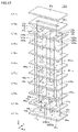
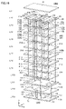
- FIG. 3 is a block diagram of a communication device having a high frequency front-end circuit to which the filter device of the first embodiment is applied. It is an equivalent circuit diagram of a filter device. It is an exploded perspective view which shows an example of the laminated structure of a filter apparatus. 2 is a diagram showing an insertion loss from an input terminal to an output terminal when the position of a joint is changed in the filter device shown in FIGS. 2 and 3. 2 is a diagram showing an insertion loss from an input terminal to an output terminal when the width of the connection electrode in the Y-axis direction is changed in the filter device shown in FIGS. 2 and 3. It is an enlarged view of the area shown in FIG. It is an equivalent circuit diagram of the filter apparatus in Embodiment 2. FIG.
- FIG. 7 It is an exploded perspective view which shows an example of the laminated structure of the filter apparatus in Embodiment 2. It is a figure which showed the insertion loss from the input terminal to the output terminal at the time of changing the position of the joint part in the filter apparatus shown with FIG. 7 and FIG. It is a figure which showed the insertion loss from the input terminal to the output terminal at the time of changing the width of the connection electrode in the Y-axis direction in the filter apparatus shown in FIGS. 7 and 8.
- FIG. 3 It is an equivalent circuit diagram of the filter apparatus in Embodiment 3.
- FIG. It is an exploded perspective view which shows an example of the laminated structure of the filter apparatus in Embodiment 3.
- FIG. It is an exploded perspective view which shows the modification 1.
- FIG. is a top view of the connection electrode provided in the modification 2.
- FIG. It is an exploded perspective view which shows the modification 3.
- FIG. It is an exploded perspective view which shows the adjustment example of
- FIG. 1 is a block diagram of a communication device 10 having a high frequency front-end circuit 20 to which the filter device of the first embodiment is applied.
- the communication device 10 is, for example, a mobile phone base station.
- the communication device 10 includes an antenna 12, a high frequency front end circuit 20, a mixer 30, a local oscillator 32, a digital-to-analog converter (DAC) 40, and an RF circuit 50. Further, the high frequency front end circuit 20 includes bandpass filters 22 and 28, an amplifier 24, and an attenuator 26. Note that FIG. 1 describes a case where the high-frequency front-end circuit 20 includes a transmission circuit that transmits a high-frequency signal from the antenna 12, but the high-frequency front-end circuit 20 is a reception circuit that receives a high-frequency signal via the antenna 12. May include.
- the communication device 10 up-converts the signal transmitted from the RF circuit 50 into a high frequency signal and radiates it from the antenna 12.
- the modulated digital signal output from the RF circuit 50 is converted into an analog signal by the D / A converter 40.
- the mixer 30 mixes the signal analog-converted by the D / A converter 40 with the oscillation signal from the local oscillator 32 and up-converts it into a high-frequency signal.
- the bandpass filter 28 removes unnecessary waves generated by up-conversion and extracts only signals in a desired frequency band.
- the attenuator 26 adjusts the strength of the transmitted signal.
- the amplifier 24 power-amplifies the transmitted signal that has passed through the attenuator 26 to a predetermined level.
- the bandpass filter 22 removes unnecessary waves generated in the amplification process and allows only signal components in the frequency band defined by the communication standard to pass through.
- the transmitted signal that has passed through the bandpass filter 22 is radiated from the antenna 12.
- a filter device corresponding to the present disclosure can be adopted.
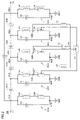
- FIG. 2 is an equivalent circuit diagram of the filter device 105.
- the filter device 105 includes an input terminal T1, an output terminal T2, and resonators RC1 to RC5.
- the resonator RC1 includes inductors L1A and L1B connected in series and capacitors C1 connected in parallel to the inductors L1A and L1B.
- the connection node N1A between the inductor L1B and the capacitor C1 is connected to the connection node N4A between the inductor L4B and the capacitor C4 via the capacitor C14. Further, the connection node N1A is connected to the connection node N2A between the inductor L2B and the capacitor C2 via the capacitor C12.
- the connection node N1B between the inductor L1A and the capacitor C1 is connected to the ground terminal GND.
- the resonator RC2 includes inductors L2A and L2B connected in series and capacitors C2 connected in parallel to the inductors L2A and L2B.
- the connection node N2A between the inductor L2B and the capacitor C2 is connected to the connection node N3A between the inductor L3B and the capacitor C3 via the capacitor C23.
- the connection node N2B between the inductor L2A and the capacitor C2 is connected to the ground terminal GND.
- the resonator RC3 includes inductors L3A and L3B connected in series and capacitors C3 connected in parallel to the inductors L3A and L3B.
- the connection node N3A between the inductor L3B and the capacitor C3 is connected to the connection node N5A between the inductor L5B and the capacitor C5 via the capacitor C35.
- the connection node N3B between the inductor L3A and the capacitor C3 is connected to the ground terminal GND.
- the resonator RC4 includes inductors L4A and L4B connected in series and capacitors C4 connected in parallel to the inductors L4A and L4B.
- the connection node N4A between the inductor L4B and the capacitor C4 is connected to the input terminal T1.
- the connection node N4B between the inductor L4A and the capacitor C4 is connected to the ground terminal GND.
- the resonator RC5 includes inductors L5A and L5B connected in series and capacitors C5 connected in parallel to the inductors L5A and L5B.
- the connection node N5A between the inductor L5B and the capacitor C5 is connected to the output terminal T2.
- the connection node N5B between the inductor L5A and the capacitor C5 is connected to the ground terminal GND.
- connection node N4A of the resonator RC4 and the connection node N5A of the resonator RC5 are connected via the capacitor C45.
- Each of the inductor L1A of the resonator RC1, the inductor L2A of the resonator RC2, and the inductor L3A of the resonator RC3 is connected to the inductor L1.
- connection node N1D of the resonator RC1 is connected to the inductor L2.
- the connection node N3D of the resonator RC3 is connected to the inductor L3.
- the inductor L2 and the inductor L3 are connected to each other.
- the connection node N1 is a connection node between the inductor L2 and the inductor L3.
- the connection node N1 is connected to the connection node N2D between the inductor L2B and the inductor L2A via the capacitor Cx.
- Each of the resonators RC1 to RC5 is an LC parallel resonator in which an inductor and a capacitor are connected in parallel. Each resonator is coupled by magnetic coupling.
- the filter device 105 has a configuration in which a five-stage resonator magnetically coupled to each other is arranged between the input terminal T1 and the output terminal T2. By adjusting the resonance frequency of each resonator, the filter device 105 functions as a bandpass filter for passing a signal in a desired frequency band.
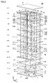
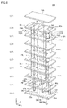
- FIG. 3 is an exploded perspective view showing an example of the laminated structure of the filter device 105.
- the filter device 105 comprises a rectangular parallelepiped or substantially rectangular parallelepiped laminate formed by laminating a plurality of dielectric layers (first layer LY1 to thirteenth layer LY13) in the stacking direction.
- Each dielectric layer of the laminate is formed of, for example, a ceramic such as low temperature co-fired ceramics (LTCC) or a resin.
- LTCC low temperature co-fired ceramics
- a plurality of electrodes formed on each dielectric layer and a plurality of vias formed between the dielectric layers form an inductor and a capacitor for forming an LC resonance circuit.
- "via” means a conductor formed in a dielectric layer for connecting electrodes formed in different dielectric layers. Vias are formed, for example, by conductive paste, plating, and / or metal pins.
- the stacking direction of the laminated body is defined as the "Z-axis direction", the direction perpendicular to the Z-axis direction and along the long side of the laminated body is defined as the "X-axis direction”, and the laminated body is short.
- the direction along the side is defined as the "Y-axis direction”.
- the positive direction of the Z axis in each figure may be referred to as an upper side, and the negative direction may be referred to as a lower side.
- a directional mark for specifying the direction of the filter device 105 may be arranged on the upper surface Sf (first layer LY1) of the laminated body.
- External terminals (input terminal T1, output terminal T2, and ground terminal GND) for connecting the filter device 105 and an external device are arranged on the lower surface Bt (13th layer LY13) of the laminated body.
- Each of the input terminal T1, the output terminal T2, and the ground terminal GND is a flat plate-shaped electrode, and is an LGA (Land Grid Array) terminal regularly arranged on the lower surface Bt of the laminated body.
- the filter device 105 has a five-stage LC parallel resonator. More specifically, the resonator RC1 formed including the via V1A, V1B, the flat plate electrode P1, the flat plate electrode P1d, and the flat plate electrode P10, and the vias V2A, V2B, the flat plate electrode P2, the flat plate electrode P2d, and the flat plate electrode Resonator RC2 formed including P11, via V3A, V3B, flat plate electrode P3, flat plate electrode P3d, and resonator RC3 formed including flat plate electrode P12, via V4A, V4B, flat plate electrode P4, flat plate.
- It includes a resonator RC4 formed including an electrode P4d and a flat plate electrode P7, and a resonator RC5 formed including a via V5A, V5B, a flat plate electrode P5, a flat plate electrode P5d, and a flat plate electrode P8.
- the flat plate electrode P7 of the resonator RC4 is formed on the 11th layer LY11.
- the flat plate electrode P7 is connected to the input terminal T1 formed on the thirteenth layer LY13 by the via V10.
- the flat plate electrode P7 of the resonator RC4 is connected to the flat plate electrode P4d formed on the third layer LY3 and the flat plate electrode P4 formed on the second layer LY2 by the via V4B.
- the flat plate electrode P4 is connected to the flat plate electrode P9 formed on the 10th layer LY10 by the via V4A.
- the plate electrode P9 is connected to the plate electrode P6 formed on the twelfth layer LY12 by the via V11.
- the flat plate electrode P6 is connected to the ground terminal GND formed in the 13th layer LY13 by the vias V6, V7, V8, V9. A part of the flat plate electrode P7 overlaps with the flat plate electrode P9 when viewed in a plan view from the stacking direction.
- the plate electrode P9 and the plate electrode P7 form the capacitor C4 of FIG. 2.
- the via V4A and the via V4B in the resonator RC4 correspond to the inductor L4A and the inductor L4B in FIG. 2, respectively.
- the flat plate electrode P8 of the resonator RC5 is formed on the 11th layer LY11.
- the flat plate electrode P8 is connected to the output terminal T2 formed on the thirteenth layer LY13 by the via V12.
- the flat plate electrode P8 of the resonator RC5 is connected to the flat plate electrode P5d formed on the third layer LY3 and the flat plate electrode P5 formed on the second layer LY2 by the via V5B.
- the flat plate electrode P5 is connected to the flat plate electrode P9 by the via V5A.
- a part of the flat plate electrode P8 overlaps with the flat plate electrode P9 when viewed in a plan view from the stacking direction.
- the plate electrode P8 and the plate electrode P9 form the capacitor C5 of FIG. 2.
- the via V5A and the via V5B in the resonator RC5 correspond to the inductor L5A and the inductor L5B in FIG. 2, respectively.
- the flat plate electrode P10 of the resonator RC1 is connected to the flat plate electrode P1d formed on the third layer LY3 and the flat plate electrode P1 formed on the second layer LY2 by the via V1B. Further, the flat plate electrode P1 is connected to the flat plate electrode P9 by the via V1A. The flat plate electrode P10 overlaps a part of the flat plate electrode P9 when viewed in a plan view from the stacking direction. The plate electrode P10 and the plate electrode P9 form the capacitor C1 in FIG. 2.
- the via V1A and the via V1B in the resonator RC1 correspond to the inductor L1A and the inductor L1B in FIG. 2, respectively.
- the flat plate electrode P11 of the resonator RC2 is connected to the flat plate electrode P2d formed on the third layer LY3 and the flat plate electrode P2 formed on the second layer LY2 by the via V2B. Further, the flat plate electrode P2 is connected to the flat plate electrode P9 by the via V2A. The flat plate electrode P11 overlaps a part of the flat plate electrode P9 when viewed in a plan view from the stacking direction. The plate electrode P9 and the plate electrode P11 form the capacitor C2 in FIG. 2.
- the via V2A and the via V2B in the resonator RC2 correspond to the inductor L2A and the inductor L2B in FIG. 2, respectively.
- the flat plate electrode P12 of the resonator RC3 is connected to the flat plate electrode P3d formed on the third layer LY3 and the flat plate electrode P3 formed on the second layer LY2 by the via V3B. Further, the flat plate electrode P3 is connected to the flat plate electrode P9 by the via V3A. The flat plate electrode P12 overlaps a part of the flat plate electrode P9 when viewed in a plan view from the stacking direction. The plate electrode P9 and the plate electrode P12 form the capacitor C3 in FIG. 2.
- the via V3A and the via V3B in the resonator RC3 correspond to the inductor L3A and the inductor L3B in FIG. 2, respectively.
- the flat plate electrodes P1d to P5d are arranged to reduce the resistance component of the flat plate electrodes P1 to P5. That is, the resistance value of the flat plate electrodes P1 to P5 is smaller in the configuration provided with the flat plate electrodes P1d to P5d as compared with the configuration not provided with the flat plate electrodes P1d to P5d.
- the via V2B of the resonator RC2 is also connected to the flat plate electrode P14 formed on the eighth layer LY8. When viewed in a plan view from the stacking direction, a part of the flat plate electrode P14 overlaps with each of the flat plate electrode P16 and the flat plate electrode P17 formed on the seventh layer LY7.
- a part of the flat plate electrode P16 overlaps the flat plate electrode P10 of the resonator RC1 with the eighth layer LY8 interposed therebetween.
- the flat plate electrode P10, the flat plate electrode P14, and the flat plate electrode P16 form the capacitor C12 in FIG. 2.
- a part of the flat plate electrode P17 overlaps the flat plate electrode P12 of the resonator RC3 with the eighth layer LY8 interposed therebetween.
- the flat plate electrode P12, the flat plate electrode P14, and the flat plate electrode P17 form the capacitor C23 in FIG. 2.
- a part of the flat plate electrode P13 connected to the flat plate electrode P7 of the resonator RC4 via the via V13 overlaps with the flat plate electrode P16.
- a part of the flat plate electrode P8 connected to the flat plate electrode P8 of the resonator RC5 via the via V14 overlaps with the flat plate electrode P17.
- each of a part of the flat plate electrode P16 and a part of the flat plate electrode P17 overlaps with the flat plate electrode P18 formed in the sixth layer LY6.
- the flat plate electrode P13, the flat plate electrode P15, the flat plate electrode P16, the flat plate electrode P17, and the flat plate electrode P18 form the capacitor C45 in FIG.
- the flat plate electrode P7 of the resonator RC4 is connected to the flat plate electrode P13 formed on the seventh layer LY7 via the via V13.
- a part of the flat plate electrode P13 overlaps with the flat plate electrode P10 of the resonator RC1.
- the plate electrode P10 and the plate electrode P13 form the capacitor C14 in FIG. 2.
- the flat plate electrode P8 of the resonator RC5 is connected to the flat plate electrode P15 formed on the seventh layer LY7 via the via V14.
- a part of the flat plate electrode P15 overlaps with the flat plate electrode P12 of the resonator RC3.
- the plate electrode P12 and the plate electrode P15 form the capacitor C35 in FIG. 2.
- Each of the via V1A of the resonator RC1, the via V2A of the resonator RC2, and the via V3A of the resonator RC3 is connected to the flat plate electrode P19 formed in the fifth layer LY5.
- the flat plate electrode P19 corresponds to the inductor L1 in FIG.
- the flat plate electrode P1 of the resonator RC1 is connected to the connection electrode CP formed in the fourth layer LY4 via the via V1. Further, the flat plate electrode P3 of the resonator RC3 is connected to the connection electrode CP via the via V2.
- the via V1 and the via V2 correspond to the inductor L2 and the inductor L3 in FIG. 2, respectively.
- a part of the connection electrode CP overlaps with the flat plate electrode P2d of the resonator RC2.
- the connection electrode CP and the flat plate electrode P2d form the capacitor Cx in FIG. 2.
- the via V1 is connected to the flat plate electrode P1 at the joint portion J1.
- the joint portion between the via V1 and the flat plate electrode P1d overlaps with the joint portion J1 when the laminated body is viewed in a plan view from the stacking direction.
- the via V2 is connected to the flat plate electrode P3 at the joint portion J2.
- the joint portion between the via V2 and the flat plate electrode P3d overlaps with the joint portion J2 when the laminated body is viewed in a plan view from the stacking direction.
- the resonators RC1 to RC5 correspond to the "first LC parallel resonator” to the "fifth LC parallel resonator” of the present disclosure, respectively.
- the flat plate electrodes P1d to P5d correspond to the "first conductor” to the "fifth conductor” of the present disclosure, respectively.
- Vias V1 and V2 correspond to the "first via” and the “second via” of the present disclosure, respectively.
- the connection electrode CP corresponds to the "connecting conductor" of the present disclosure.
- the width of the connection electrode CP is the width of the connection electrode CP on the XY plane of the second layer LY2 in the Y-axis direction. In the following, it may be simply referred to as the width of the connection electrode CP.
- the filter device 105 by moving the positions of the junctions J1 and J2 in the Y-axis direction, the strength of the magnetic coupling between the resonators RC1 and RC3 can be changed, and the inductor L2 and the inductor L2 can be changed.
- the inductance of L3 can be adjusted.
- the filter device 105 is provided with the connection electrode CP, the width of the connection electrode CP can be changed to adjust the capacitance of the capacitor Cx in FIG. 2, and the arrangement of the connection electrode CP can be changed in the figure.
- the inductance of the inductors L2 and L3 of 2 can be adjusted. That is, the capacitance of the capacitor Cx and the inductance of the inductors L2 and L3 can be used as parameters for adjusting the strength of the electromagnetic field coupling between the resonators.
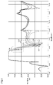
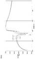
- FIG. 4 shows from the input terminal T1 to the output terminal T2 when the position of the joint portion J1 on the flat plate electrode P1 and the position of the joint portion J2 on the flat plate electrode P3 are changed in the filter device 105 shown in FIGS. 2 and 3. It is a figure which showed the insertion loss.
- the positions of the joints J1 and J2 are changed, the positions are changed so that the via V1, the connection electrode CP, and the via V2 slide in the Y-axis direction while maintaining the shape shown in FIG. means.
- solid lines Ln1 to Ln5 showing the insertion loss of the filter device 105 in which the positions of the joint portions J1 and J2 are different are displayed.
- the solid line Ln3 shows the insertion loss when the joints J1 and J2 are located near the center in the Y-axis direction of the flat plate electrodes P1 and P2.
- the solid line Ln2 shows the insertion loss when the joints J1 and J2 are located on the negative side of the Y axis with respect to the joints J1 and J2 of the solid line Ln3.
- the solid line Ln1 indicates an insertion loss when the joints J1 and J2 are located on the negative side of the Y axis with respect to the joints J1 and J2 of the solid line Ln2.
- the solid line Ln4 indicates the insertion loss when the joints J1 and J2 are located on the positive side of the Y axis with respect to the joints J1 and J2 of the solid line Ln3.
- the solid line Ln5 shows the insertion loss when the joints J1 and J2 are located further on the positive side of the Y axis than the joints J1 and J2 of the solid line Ln2.
- each of the solid lines Ln1 to Ln5 has an attenuation pole D1 and an attenuation pole D2.
- the magnetic coupling between the resonators RC1 and RC3 is larger than the capacitive coupling between the resonators RC1 and RC3. Therefore, the attenuation poles D1 and D2 are formed on the high frequency side of the pass band.
- junctions J1 and J2 are located on the negative side of the Y-axis, the positions of the junctions J1 and J2 are closer to the ground terminal GND side, so that the magnetic coupling between the resonator RC1 and the resonator RC3 becomes smaller. .. Therefore, the amount of attenuation of the attenuation pole D1 becomes large, and the frequency of the attenuation pole D2 becomes low.
- junctions J1 and J2 are located on the positive side of the Y axis, the positions of the junctions J1 and J2 are closer to the input terminal T1 side, so that the magnetic coupling between the resonator RC1 and the resonator RC3 becomes larger. .. Therefore, the amount of attenuation of the attenuation pole D1 becomes small, and the frequency of the attenuation pole D2 becomes high.
- the inductances of the inductor L2 and the inductor L3 change, and the frequency of the attenuation pole D2 changes.
- the amount of attenuation of the attenuation pole D1 changes. That is, when the frequency of the attenuation pole D2 becomes low, the frequency of the attenuation pole D2 approaches the frequency of the attenuation pole D1.
- the smaller the frequency difference between the attenuation pole D1 and the attenuation pole D2 the stronger the influence from the attenuation pole D2, and the larger the attenuation amount of the attenuation pole D1.
- the larger the frequency difference between the attenuation pole D1 and the attenuation pole D2 the smaller the influence from the attenuation pole D2, and the smaller the amount of attenuation of the attenuation pole D1.
- the inductances of the inductor L2 and the inductor L3 are changed by changing the positions of the junctions J1 and J2 of the flat plate electrode P1 and the flat plate electrode P2 in the Y-axis direction. , The amount of attenuation of the attenuation electrode D1 and the frequency band of the attenuation electrode D2 can be adjusted.
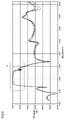
- FIG. 5 is a diagram showing the insertion loss from the input terminal T1 to the output terminal T2 when the width of the connection electrode CP, that is, the capacitance of the capacitor Cx is changed in the filter device 105 shown in FIGS. 2 and 3. ..
- FIG. 6 is an enlarged view of the region VI shown in FIG. In FIGS. 5 and 6, solid lines Ln6 to Ln9 showing the insertion loss of the filter devices 105 having different widths of the connection electrode CP in the Y-axis direction are displayed.
- the solid line Ln6 shows the insertion loss of the filter device 105 of FIG.
- the solid line Ln7 shows the insertion loss when the width of the connection electrode CP is wider than the width of the connection electrode CP of the filter device 105 of FIG.
- the solid line Ln8 shows the insertion loss when the width of the connection electrode CP is wider than the width of the connection electrode CP in the solid line Ln7.
- the solid line Ln9 shows the insertion loss when the width of the connection electrode CP is wider than the width of the connection electrode CP in the solid line Ln8.
- the attenuation poles D1 indicated by the solid lines Ln6 to Ln9 are formed at different positions from each other.
- the wider the width of the connection electrode CP in the Y-axis direction the smaller the amount of attenuation of the attenuation pole D1. Further, the narrower the width of the connection electrode CP in the Y-axis direction, the larger the amount of attenuation of the attenuation pole D1.
- the capacitor Cx in FIG. 2 is formed by the connection electrode CP of FIG. 3 and the flat plate electrode P2d. That is, the capacitance of the capacitor Cx changes by changing the width of the connection electrode CP in the Y-axis direction. As a result, the amount of attenuation of the attenuation pole D1 changes.
- the filter device 105 of the first embodiment it is possible to adjust the attenuation amount and the frequency of the attenuation pole by changing the width and arrangement of the connection electrode CP.
- At least one of the attenuation amount and the frequency of the attenuation pole can be adjusted by adjusting the capacitance of the capacitor Cx and the inductance of the inductor L2 and the inductor L3. That is, in the filter device 105 of the present disclosure, the capacitance of the capacitor Cx and the inductance of the inductor L2 and the inductor L3 can be used as parameters of the electromagnetic field coupling between the resonators. As a result, the ability to adjust the electromagnetic field coupling between the LC parallel resonators can be expanded, and the realizability of the desired pass characteristics can be enhanced.
- a filter device 105 including a five-stage LC parallel resonator including a connection electrode CP for connecting the resonator RC1 and the resonator RC2 has been described.
- a three-stage LC parallel resonator including a connection electrode CPt for connecting the resonator RC1 and the resonator RC3 will be described with reference to FIGS. 7 and 8.
- FIG. 7 is an equivalent circuit diagram of the filter device 103 according to the second embodiment.
- the filter device 103 of FIG. 7 has a configuration in which the resonator RC4 and the resonator RC5 are removed from the filter device 105 of FIG. That is, the filter device 103 has a configuration in which three-stage resonators RC1 to RC3 that are magnetically coupled to each other are arranged. Further, the filter device 103 of FIG. 7 has a configuration excluding the inductor L1 connecting between the connection node N1C, the connection node N2C, and the connection node N3C of the filter device 105 of FIG. The connection node N1A between the capacitor C1 and the inductor L1B is connected to the connection node N3A between the capacitor C3 and the inductor L3B via the capacitor C13.
- At least one of the attenuation pole attenuation amount and frequency adjustment by changing the positions of the junctions J1 and J2 and the width of the connection electrode CP excludes the resonator RC4, the resonator RC5, and the inductor L1. Even a configuration can be realized.
- FIG. 8 is an exploded perspective view showing an example of the laminated structure of the filter device 103 in the second embodiment.
- the filter device 103 includes a rectangular parallelepiped or substantially rectangular parallelepiped laminate formed by laminating a plurality of dielectric layers (first layer LY1t to tenth layer LY10t) in the stacking direction. There is.
- a directional mark for specifying the direction of the filter device 103 may be arranged on the upper surface Sft (first layer LY1t) of the laminated body.
- External terminals (input terminal T1t, output terminal T2t, and ground terminal GND1t, GND2t) for connecting the filter device 103 and an external device are arranged on the lower surface Btt (10th layer LY10t) of the laminated body.
- the filter device 103 includes a three-stage LC parallel resonator. More specifically, the resonator RC1 formed by including the via V1At, V1Bt, the flat plate electrode P1t and the flat plate electrode P4t, and the resonator RC2 formed by including the via V2At, V2Bt, the flat plate electrode P2t and the flat plate electrode P8t. And the resonator RC3 formed by including the vias V3At, V3Bt, the plate electrode P3t and the plate electrode P6t.
- the flat plate electrode P4t is connected to the input terminal T1t formed on the 10th layer LY10t by the via V4t.
- the flat plate electrode P4t of the resonator RC1 is connected to the flat plate electrode P1t formed on the second layer LY2t by the via V1Bt.
- the flat plate electrode P1t is connected to the flat plate electrode P7t formed on the eighth layer LY8t by the via V1At.
- the flat plate electrode P7t is connected to the flat plate electrode P5t formed on the ninth layer LY9t by the via V8t.
- the flat plate electrode P5t is connected to the ground terminals GND1t and GND2t formed in the 10th layer LY10t by the vias V5t and V6t, respectively.
- a part of the flat plate electrode P4t overlaps with the flat plate electrode P7t.
- the flat plate electrode P4t and the flat plate electrode P7t form the capacitor C1 in FIG. 7.
- the via V1At and the via V1Bt in the resonator RC1 correspond to the inductor L1A and the inductor L1B in FIG. 7, respectively.
- the flat plate electrode P8t of the resonator RC2 is connected to the flat plate electrode P2t formed on the second layer LY2t by the via V2Bt. Further, the flat plate electrode P2t is connected to the flat plate electrode P7t by the via V2At. A part of the flat plate electrode P7t overlaps with the flat plate electrode P8t when viewed in a plan view from the stacking direction.
- the flat plate electrode P7t and the flat plate electrode P8t form the capacitor C2 in FIG. 7.
- the via V2At and the via V2Bt in the resonator RC2 correspond to the inductor L2A and the inductor L2B in FIG. 7, respectively.
- the flat plate electrode P6t of the resonator RC3 is formed on the 9th layer LY9t.
- the flat plate electrode P6t is connected to the output terminal T2t formed on the 10th layer LY10t by the via V7t.
- the flat plate electrode P6t is connected to the flat plate electrode P3t formed on the second layer LY2t by the via V3Bt. Further, the flat plate electrode P3t is connected to the flat plate electrode P7t by the via V3At.
- a part of the flat plate electrode P7t overlaps with the flat plate electrode P6t when viewed in a plan view from the stacking direction.
- the flat plate electrode P6t and the flat plate electrode P7t form the capacitor C3 in FIG. 7.
- the via V3At and the via V3Bt in the resonator RC3 correspond to the inductor L3A and the inductor L3B in FIG. 7, respectively.
- a part of the flat plate electrode P8t of the resonator RC2 overlaps with the flat plate electrode P9t formed on the sixth layer LY6t.
- the plate electrode P9t is connected to the plate electrode P4t of the resonator RC1 via the via V9t.
- the flat plate electrode P8t and the flat plate electrode P9t form the capacitor C12 in FIG. 7.
- a part of the flat plate electrode P8t of the resonator RC2 overlaps with the flat plate electrode P10t formed on the sixth layer LY6t.
- the plate electrode P10t is connected to the plate electrode P6t of the resonator RC3 via the via V10t.
- the flat plate electrode P8t and the flat plate electrode P10t form the capacitor C23 in FIG. 7.
- the flat plate electrode P11t formed on the fifth layer LY5t when viewed in a plan view from the stacking direction overlaps with each of the flat plate electrode P9t and the flat plate electrode P10t.
- the flat plate electrode P9t, the flat plate electrode P10t, and the flat plate electrode P11t form the capacitor C13 in FIG. 7.
- the flat plate electrode P1t of the resonator RC1 is connected to the connection electrode CPt formed on the third layer LY3t via the via V1t. Further, the flat plate electrode P3t of the resonator RC3 is connected to the connection electrode CPt via the via V2t.
- the via V1t and the via V2t correspond to the inductor L2 and the inductor L3 in FIG. 7, respectively.
- a part of the connection electrode CPt overlaps with the flat plate electrode P2t of the resonator RC2.
- the capacitor Cx in FIG. 7 is formed by the connection electrode CPt and the flat plate electrode P2t.
- the via V1t is connected to the flat plate electrode P1t at the joint portion J1t.
- the via V2t is connected to the flat plate electrode P3t at the joint portion J2t.
- FIG. 9 is a diagram showing an insertion loss from the input terminal T1t to the output terminal T2t when the positions of the joint portions J1t and J2t are changed in the filter device 103 shown in FIGS. 7 and 8.
- solid lines Ln10 to Ln12 showing the insertion loss of the filter device 103 in which the positions of the joint portions J1t and J2t are different are displayed.
- the solid line Ln11 indicates the insertion loss when the positions of the joint portions J1t and J2t are near the center in the Y-axis direction of the flat plate electrode P1t and the flat plate electrode P3t.
- the solid line Ln10 indicates the insertion loss when the joint portions J1t and J2t are located on the negative direction side in the Y-axis direction with respect to the joint portions J1t and J2t of the solid line Ln10.
- the solid line Ln12 shows the insertion loss when the joints J1t and J2t are located on the positive side in the Y-axis direction with respect to the joints J1t and J2t of the solid line Ln11.
- Each of the solid lines Ln10 to Ln12 has an attenuation pole D3.
- the capacitive coupling between the resonators RC1 and RC3 is larger than the magnetic coupling between the resonators RC1 and RC3. Therefore, the attenuation pole D3 is formed on the low frequency side of the pass band.
- the inductances of the inductor L2 and the inductor L3 in FIG. 7 change by changing the positions of the junctions J1t and J2t.
- the frequency of the attenuation pole D3 changes.
- the inductances of the inductor L2 and the inductor L3 are changed by changing the positions of the junctions J1t and J2t of the flat plate electrode P1t and the flat plate electrode P3t in the Y-axis direction. , The amount of attenuation and the frequency band of the attenuation electrode D3 can be adjusted.
- FIG. 10 is a diagram showing an insertion loss from the input terminal T1t to the output terminal T2t when the width of the connection electrode CPt in the Y-axis direction is changed in the filter device 103 shown in FIGS. 7 and 8.
- solid lines Ln13 to Ln15 showing the insertion loss of the filter devices 103 having different widths of the connection electrodes CPt in the Y-axis direction are displayed.
- the solid line Ln13 shows the insertion loss of the filter device 103 shown in FIG.
- the solid line Ln14 shows the insertion loss when the width of the connection electrode CPt is wider than the width of the connection electrode CPt of the filter device 103 shown in FIG.
- the solid line Ln15 shows the insertion loss when the width of the connection electrode CPt is wider than the width of the connection electrode CPt in the solid line Ln14.
- Each of the solid lines Ln10 to Ln12 has an attenuation pole D3.
- the attenuation amount and the frequency band of the attenuation pole D3 are adjusted by changing the positions of the joint portions J1t and J2t and the width of the connection electrode CPt in the Y-axis direction. be able to. That is, in the filter device 103 of the second embodiment, the capacitance of the capacitor Cx and the inductances of the inductor L2 and the inductor L3 can be used as parameters of the electromagnetic field coupling between the resonators. Thereby, even in the electromagnetic field coupling between the three-stage LC parallel resonators as shown in the second embodiment, the adjustment ability can be expanded and the feasibility of the desired passing characteristic can be enhanced.
- the resonators RC1 to RC3 in the second embodiment correspond to the "first LC parallel resonator” to the "third LC parallel resonator” of the present disclosure, respectively.
- the flat plate electrodes P1t to P3t correspond to the "first conductor” to the "third conductor” of the present disclosure, respectively.
- the vias V1t and V2t correspond to the "first via” and the “second via” of the present disclosure, respectively.
- the connection electrode CPt corresponds to the "connecting conductor" of the present disclosure.
- the filter device 103 including the three-stage LC parallel resonator has been described.
- the filter device 104 including the four-stage LC parallel resonator will be described with reference to FIGS. 11 and 12.
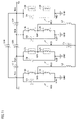
- FIG. 11 is an equivalent circuit diagram of the filter device 104 according to the third embodiment.
- the filter device 104 of FIG. 11 has a configuration in which the resonator RC4 is added to the filter device 103 of FIG. That is, the filter device 104 has a configuration in which four-stage resonators RC1 to RC4 that are magnetically coupled to each other are arranged.
- the connection node N3A between the inductor L3B and the capacitor C3 is connected to the connection node N4A between the inductor L4B and the capacitor C4 via the capacitor C34.
- the connection node N1A between the inductor L1A and the capacitor C1 was connected to the connection node N3A in the second embodiment, but is connected to the connection node N4A via the capacitor C14 in the third embodiment.
- the attenuation amount and frequency of the attenuation electrode by changing the positions of the junctions J1f and J2f and the width of the connection electrode CPf in the Y-axis direction shown in FIG. Adjustment can be achieved.
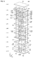
- FIG. 12 is an exploded perspective view showing an example of the laminated structure of the filter device 104 in the third embodiment.
- the filter device 104 of FIG. 12 has a four-stage LC parallel resonator. More specifically, the resonator RC1 formed by including the via V1Af, V1Bf, the flat plate electrode P1f, the flat plate electrode P1df, and the flat plate electrode P6f, and the via V2Af, V2Bf, the flat plate electrode P2f, the flat plate electrode P2df, and the flat plate electrode.
- Resonator RC2 formed including P9f
- resonator RC3 formed including via V3Af, V3Bf, flat plate electrode P3f, flat plate electrode P3df, and flat plate electrode P10f, via V4Af, V4Bf, flat plate electrode P4f, flat plate. It includes an electrode P4df and a resonator RC4 formed including a flat plate electrode P7f.
- the flat plate electrode P6f of the resonator RC1 is formed on the 9th layer LY9f.
- the flat plate electrode P6f is connected to the input terminal T1f formed on the 11th layer LY11f by the via V9f.
- the flat plate electrode P6f of the resonator RC1 is connected to the flat plate electrode P1df formed on the third layer LY3f and the flat plate electrode P1f formed on the second layer LY2f by the via V1Bf.
- the flat plate electrode P1f is connected to the flat plate electrode P8f formed on the eighth layer LY8f by the via V1Af.
- the flat plate electrode P8f is connected to the flat plate electrode P5f formed on the 10th layer LY10f by the via V10f.
- the flat plate electrode P5f is connected to the ground terminal GNDf formed on the 11th layer LY11f by the vias V5f, V6f, V7f, and V8f. A part of the flat plate electrode P6f also overlaps with the flat plate electrode P8f when viewed in a plan view from the stacking direction.
- the flat plate electrode P6f and the flat plate electrode P8f form the capacitor C1 in FIG. 11.
- the flat plate electrode P9f of the resonator RC2 is connected to the flat plate electrode P2df formed on the third layer LY3f and the flat plate electrode P2f formed on the second layer LY2f by the via V2Bf. Further, the flat plate electrode P2f is connected to the flat plate electrode P8f formed on the eighth layer LY8f by the via V2Af. A part of the flat plate electrode P8f overlaps with the flat plate electrode P9f when viewed in a plan view from the stacking direction. The flat plate electrode P8f and the flat plate electrode P9f form the capacitor C2 in FIG. 11.
- the flat plate electrode P10f of the resonator RC3 is connected to the flat plate electrode P3df formed on the third layer LY3f and the flat plate electrode P3f formed on the second layer LY2f by the via V3Bf. Further, the flat plate electrode P3f is connected to the flat plate electrode P8f formed on the eighth layer LY8f by the via V3Af. A part of the flat plate electrode P8f overlaps with the flat plate electrode P10f when viewed in a plan view from the stacking direction. The flat plate electrode P8f and the flat plate electrode P10f form the capacitor C3 in FIG. 11.
- the flat plate electrode P7f of the resonator RC4 is formed on the 9th layer LY9f.
- the flat plate electrode P7f is connected to the output terminal T2f formed on the 11th layer LY11f by the via V11f.
- the flat plate electrode P7f of the resonator RC4 is connected to the flat plate electrode P4df formed on the third layer LY3f and the flat plate electrode P4f formed on the second layer LY2f by the via V4Bf.
- the flat plate electrode P4f is connected to the flat plate electrode P8f formed on the eighth layer LY8f by the via V4Af.
- a part of the flat plate electrode P8f overlaps with the flat plate electrode P7f when viewed in a plan view from the stacking direction.
- the flat plate electrode P7f and the flat plate electrode P8f form the capacitor C4 in FIG. 11.
- the plate electrode P11f is connected to the plate electrode P6f of the resonator RC1 via the via V12f.
- a part of the flat plate electrode P10f of the resonator RC3 overlaps with the flat plate electrode P12f formed on the sixth layer LY6f when viewed in a plan view from the stacking direction.
- the plate electrode P12f is connected to the plate electrode P7f of the resonator RC4 via the via V13f.
- the flat plate electrode P10f and the flat plate electrode P12f form the capacitor C34 in FIG. 11.
- the capacitor C14 in FIG. 11 is formed by the flat plate electrode P11f, the flat plate electrode P12f, and the flat plate electrode P13f formed on the fifth layer LY5f.
- the flat plate electrode P9f, the flat plate electrode P10f, the flat plate electrode P11f, the flat plate electrode P12f, and the flat plate electrode P13f form the capacitor C23 in FIG.
- the flat plate electrode P1df of the resonator RC1 is connected to the connection electrode CPf formed on the fourth layer LY4f via the via V1f. Further, the flat plate electrode P3df of the resonator RC3 is connected to the connection electrode CPf via the via V2f.
- the via V1f and the via V2f correspond to the inductor L2 and the inductor L3 in FIG. 11, respectively.
- a part of the connection electrode CPf overlaps with the flat plate electrode P2df of the resonator RC2.
- the capacitor Cx in FIG. 11 is formed by the connection electrode CPf and the flat plate electrode P2df.
- the via V1f is connected to the flat plate electrode P1f at the joint portion J1f.
- the joint portion between the via V1f and the flat plate electrode P1df overlaps with the joint portion J1f when the laminated body is viewed in a plan view from the stacking direction.
- the via V2f is connected to the flat plate electrode P3f at the joint portion J2f.
- the joint portion between the via V2f and the flat plate electrode P3df overlaps with the joint portion J2f when the laminated body is viewed in a plan view from the stacking direction.
- the attenuation electrode is changed by changing the positions of the junctions J1f and J2f and the width of the connection electrode CPf.
- the attenuation and frequency band of the can be adjusted. That is, the capacitance of the capacitor Cx and the inductances of the inductor L2 and the inductor L3 can be used as parameters for electromagnetic field coupling between the resonators.
- the adjustment ability can be expanded even in the electromagnetic field coupling between the four-stage LC parallel resonators shown in the third embodiment, and the feasibility of the desired passage characteristics can be enhanced.
- FIG. 13 is an exploded perspective view showing a modified example 1.
- connection electrode CPu is arranged on the positive direction side of the Z axis with respect to the flat plate electrode P2u as compared with the filter device 103 shown in FIG. That is, the connection electrode CPU is formed on the second layer LY2u.
- the flat plate electrode P2u is formed on the third layer LY3u. That is, in the stacking direction, the flat plate electrode P2u is formed between the ground terminals GND1u and GND2u and the connection electrode CPu.
- the via V1u and the via V2u are formed between the second layer LY2u and the third layer LY3u.
- the filter device 103A shown in FIG. 13 has the same characteristics as the filter device 103 shown in FIG. 8, but the via V1u is formed between layers different from the vias V1Au and V1Bu.
- the filter device 103A it is possible to prevent electrical interference from occurring between the via V1u and the vias V1Au and V1Bu.
- the filter device 103A it is possible to prevent electrical interference from occurring between the via V2u and the vias V2Au and V2Bu.
- the filter device 103A since the via V1u and the vias V1Au and V1Bu are formed between different layers, no physical interference occurs. Therefore, the region in which the position of the plate electrodes P1u and P2u of the joints J1u and J2u can be changed in the Y-axis direction is wider than that of the filter device 103 of FIG. That is, in the filter device 103A, the degree of freedom in arranging the via V1u and the via V2u is improved.
- the attenuation amount and the frequency band of the attenuation electrode can be adjusted by providing the connection electrode CPu which overlaps with the flat plate electrode P2u when viewed in a plan view from the stacking direction. .. That is, the capacitance of the capacitor Cx and the inductances of the inductor L2 and the inductor L3 can be used as parameters for electromagnetic field coupling between the resonators. As a result, the adjustment ability can be expanded even in the electromagnetic field coupling between the three-stage LC parallel resonators shown in the first modification, and the feasibility of the desired passing characteristics can be enhanced.
- the flat plate electrodes P1u to P3u correspond to the "first conductor” to the "third conductor” of the present disclosure, respectively.
- the vias V1u and V2u correspond to the "first via” and the “second via” of the present disclosure, respectively.
- the connection electrode CPU corresponds to the "connecting conductor" of the present disclosure.
- FIG. 14 is an exploded perspective view showing a modification 2.
- the resonator RC4 is arranged between the resonator RC2 and the resonator RC3. That is, in the filter device 105 of the first embodiment, the resonators are arranged in the order of RC4, RC1, RC2, RC3, RC5, whereas in the filter device 105A of the modification 2, the resonators are RC1, RC2. , RC4, RC3, RC5.
- the connection electrode CPa connects the resonator RC1 and the resonator RC3 via vias V1a and V2.
- the filter device 105A includes a resonator RC1 formed including a via V1Aa, V1Ba, a flat plate electrode P1a, a flat plate electrode P1da, and a flat plate electrode P7, and vias V2Aa, V2Ba, a flat plate electrode P2a, a flat plate electrode P2da, and a flat plate electrode P10.
- RC2 formed including the via V4Aa, V4Ba, a flat plate electrode P4a, a flat plate electrode P4da, and a resonator RC4 formed including the flat plate electrode P11, and a via V3A, V3B, a flat plate electrode P3, and a flat plate electrode.
- It includes a resonator RC3 formed including P3d and a flat plate electrode P12, and a resonator RC5 formed including vias V5A, V5B, a flat plate electrode P5, a flat plate electrode P5d, and a flat plate electrode P8.
- the resonator RC4 also changes the positions of the junctions J1a and J2 and the width of the connection electrode CPa in the Y-axis direction in the filter device 105A arranged between the resonator RC2 and the resonator RC3.
- the attenuation amount and the frequency band of the attenuation pole can be adjusted as in the first embodiment.
- the adjustment ability can be expanded even in the electromagnetic field coupling between the four-stage LC parallel resonators shown as the second modification, and the feasibility of the desired passing characteristics can be enhanced.
- FIG. 15 is a plan view of the connection electrode CPa provided in the modification 2.
- the width of the connection electrode CP shown in FIG. 3 in the Y-axis direction was a uniform length in all regions of the connection electrode CP.
- the attenuation amount and the frequency of the attenuation pole are adjusted by changing the capacitance between the filter device 105 and the capacitor Cx.
- the width in the Y-axis direction of the regions R1 and R2 of the connection electrodes CPa overlapping with the flat plate electrodes P2da and P4da when the laminated body is viewed in a plan view from the stacking direction is wider than the width of the regions other than the regions R1 and R2. is doing.
- the flat plate electrodes P1da, P2da, P4da, P3, P5 and the connecting conductor CPa are transmitted when the laminated body is viewed in a plan view.
- the length of the width of the connection electrode CPa in the Y-axis direction of the region R1 is the width W2.
- the length of the width of the connection electrode CPa in the Y-axis direction of the region R2 is the width W3.
- the length of the width of the region other than the width W1 and the width W2 is the width W1.
- the capacitance of the capacitor formed between the connection electrode CPa and the flat plate electrodes P2da and P4da can be adjusted by changing the width of the connection electrode CPa.
- the amount and frequency of attenuation of the attenuation electrode can be adjusted.
- the cost of the connection electrode CPa is reduced by widening only the area required for adjusting the capacitance.
- the resonators RC1 to RC5 correspond to the "first LC parallel resonator” to the "fifth LC parallel resonator” of the present disclosure, respectively.
- the flat plate electrodes P1da, P2da, P3d, P4da, and P5d correspond to the "first conductor” to the "fifth conductor” of the present disclosure, respectively.
- the vias V1a and V2 correspond to the "first via” and the “second via” of the present disclosure, respectively.
- the connection electrode CPa corresponds to the "connecting conductor” of the present disclosure.
- Region R1 corresponds to the "first region” of the present disclosure.
- the width W2 corresponds to the "first width” of the present disclosure.
- the width W1 corresponds to the "second width" of the present disclosure.
- Modification 3 In the first embodiment, a configuration in which two vias, vias V1 and V2, are connected to the connection electrode CP has been described. However, the number of vias connected to the connection electrode CP is not limited to two. Hereinafter, a configuration in which three vias are connected to the connection electrode CP will be described.
- FIG. 16 is an exploded perspective view showing a modified example 3.
- the filter device 105B of the third modification three vias V1b to V3b are connected to the connection electrode CPb.
- the via V1b is connected to the flat plate electrode P1b at the joint portion J1b.
- the via V2b is connected to the flat plate electrode P3b at the joint portion J2b.
- the via V3b is connected to the flat plate electrode P7 at the joint portion J3b.
- the filter device 105B of the modification 3 has a configuration in which the resonators RC4 and RC5 are removed from the filter device 105 of FIG. 3, and the resonators RC6 and RC7 are newly added.
- a capacitor Cy (not shown) is also formed between the flat plate electrode P6d and the connection electrode CPb.
- the inductor L4 (not shown) corresponding to the via V3b is formed.
- the filter device 105B of the modification 3 not only the capacitance of the capacitor Cx but also the capacitance of the capacitor Cy can be adjusted, and further, not only the inductor L2 and the inductor L3 but also the inductor L4 can be adjusted, and the attenuation of the attenuation pole is attenuated.
- the amount and frequency can be fine-tuned.
- FIG. 3 has described an example in which the positions of the via V1, the connection electrode CP, and the via V2 are changed so as to slide in the Y-axis direction while maintaining the shape shown in FIG.
- the position of only one of the joint portions J1 and J2 may be changed, or the positions of the joint portions J1 and J2 in the Y-axis direction may be changed so as to be different from each other.
- FIG. 17 is an exploded perspective view showing an adjustment example of the modified example 3.
- the filter device 105BZ of FIG. 17 is an example in which the joint portions J1b and J3b of the filter device 105B of FIG. 16 are adjusted.
- the joint portions J1b and J3b in FIG. 17 are located on the positive direction side of the Y axis in the flat plate electrodes P1b and P7 with respect to the joint portions J1b and J3b in FIG.
- the vias V1b and V2b are located on the positive direction side of the Y axis, and the connection electrode CPb has a V-shaped shape.
- the attenuation amount and frequency of the attenuation pole can be finely adjusted by adjusting each of the junctions J1b to J3b separately and adjusting the inductor and the capacitor. ..
- the flat plate electrodes P1db, P2db, and P3db correspond to the "first conductor” to "third conductor” of the present disclosure, respectively.
- the flat plate electrodes P6d and P7d correspond to the "sixth conductor” and the “seventh conductor” of the present disclosure, respectively.
- the vias V1b to V3b correspond to the "first via” to the "third via” of the present disclosure, respectively.
- the connection electrode CPb corresponds to the "connecting conductor" of the present disclosure.
Landscapes
- Engineering & Computer Science (AREA)
- Power Engineering (AREA)
- Microelectronics & Electronic Packaging (AREA)
- Manufacturing & Machinery (AREA)
- Filters And Equalizers (AREA)
- Coils Or Transformers For Communication (AREA)
Abstract
フィルタ装置(105)であって、複数の誘電体層(LY1~LY13)が積層された積層体と、接地端子(GND)と、積層体に形成され、互いに磁気結合する第1LC並列共振器(RC1)、第2LC並列共振器(RC2)および第3LC並列共振器(RC3)とを備える。第1LC並列共振器(RC1)は第1導体(P1d)を含み、第2LC並列共振器(RC2)は第2導体(P2d)を含み、第3LC並列共振器(RC3)は第3導体(P3d)を含む。フィルタ装置(105)は、第2導体(P2d)と異なる層に形成された接続導体(CP)と一方端が第1導体(P1d)に接続され他方端が接続導体(CP)に接続された第1ビア(V1)と、一方端が第3導体(P3d)に接続され他方端が接続導体(CP)に接続された第2ビア(V2)とをさらに備える。接続導体(CP)は、積層体を積層方向から平面視した場合に、第2導体(P2d)の一部と重なる第1領域(R1)を含む。
Description
本開示はフィルタ装置およびそれを備える高周波フロントエンド回路に関し、より特定的には、積層LCフィルタの特性を向上させるための技術に関する。
国際公開第2016/092903号(特許文献1)には、3つ以上のLC並列共振器が並んだ構成を備えるフィルタ装置において、隣り合わない2つのLC並列共振器が磁界結合することを特徴とするバンドパスフィルタが開示されている。
特許文献1では、隣り合わない2つのLC並列共振器が磁界結合することによって、減衰極の減衰量を大きくするとともに、通過帯域の両端における挿入損失の急峻性が改善された通過特性を実現している。
近年、様々な周波数帯の信号が通信において利用されるようになり、特定の周波数帯の信号を送受信する際に他の周波数帯の信号との干渉を避けつつ、所望の通過特性を実現することが可能なフィルタ装置が求められている。
本開示は、このような課題を解決するためになされたものであり、その目的は、3つ以上のLC並列共振器を備えるフィルタ装置において、複数のLC並列共振器の間の電磁界結合の調整能力を拡大して、所望の通過特性を実現することである。
本開示のある局面に従うフィルタ装置は、複数の誘電体層が積層された積層体と、接地端子と、積層体に形成され、互いに磁気結合する第1LC並列共振器、第2LC並列共振器および第3LC並列共振器とを備える。第1LC並列共振器、第2LC並列共振器および第3LC並列共振器の各々は、接地端子に接続されており、第1LC並列共振器は、第1導体を含み、第2LC並列共振器は、第2導体を含み、第3LC並列共振器は、第3導体を含む。フィルタ装置は、第2導体と異なる層に形成された接続導体と、一方端が第1導体に接続され、他方端が接続導体に接続された第1ビアと、一方端が第3導体に接続され、他方端が接続導体に接続された第2ビアとをさらに備える。接続導体は、積層体を積層方向から平面視した場合に、第2導体の一部と重なる第1領域を含む。
本開示の他の局面に従うフィルタ装置は、接地端子と、各々が接地端子に接続され、互いに電気的に接続された複数のLC並列共振器とを備える。複数のLC並列共振器は、第1LC並列共振器、第2LC並列共振器および第3LC並列共振器を含む。複数のLC並列共振器の各々は、直列接続された第1インダクタおよび第2インダクタと第1キャパシタとを含み、第2インダクタおよび第1キャパシタの間の接続ノードにおいて接地端子と接続する。フィルタ装置は、第1LC並列共振器における第1インダクタおよび第2インダクタの間の接続ノードと第3LC並列共振器における第1インダクタおよび第2インダクタの間の接続ノードとの間に直列に接続された第3インダクタおよび第4インダクタと、第2LC並列共振器における第1インダクタおよび第2インダクタの間の接続ノードと、第3インダクタおよび第4インダクタの間の接続ノードとの間に接続された第2キャパシタとをさらに備える。
本開示によるフィルタ装置において、互いに磁気結合する第1LC並列共振器、第2LC並列共振器および第3LC並列共振器とを備える。第1LC並列共振器と第3LC並列共振器とが、接続導体を介して磁気結合される。第2LC並列共振器は第2導体を含む。積層体を積層方向から平面視した場合に接続導体が第2導体の一部と重なることにより、接続導体は第2導体と容量結合をする。
このような構成とすることによって、接続導体が配置されない場合と異なり、接続導体と第2導体との間でキャパシタが形成され、第1LC並列共振器と第3LC並列共振器との間にインダクタを形成する。
当該キャパシタの容量およびインダクタのインダクタンスを調整することにより、第1LC並列共振器、第2LC並列共振器および第3LC並列共振器の間の電磁界結合を調整することができ、当該キャパシタの容量およびインダクタのインダクタンスは、電磁界結合のパラメータとして利用することができる。
したがって、LC並列共振器間の電磁界結合の調整能力を拡大することができるので、所望の通過特性の実現可能性を高めることができる。
以下、本開示の実施の形態について、図面を参照しながら詳細に説明する。なお、図中同一または相当部分には同一符号を付してその説明は繰り返さない。
[実施の形態1]
(通信装置の基本構成)
図1は、実施の形態1のフィルタ装置が適用される高周波フロントエンド回路20を有する通信装置10のブロック図である。通信装置10は、たとえば、携帯電話基地局である。
(通信装置の基本構成)
図1は、実施の形態1のフィルタ装置が適用される高周波フロントエンド回路20を有する通信装置10のブロック図である。通信装置10は、たとえば、携帯電話基地局である。
図1を参照して、通信装置10は、アンテナ12と、高周波フロントエンド回路20と、ミキサ30と、局部発振器32と、D/Aコンバータ(DAC)40と、RF回路50とを備える。また、高周波フロントエンド回路20は、バンドパスフィルタ22,28と、増幅器24と、減衰器26とを含む。なお、図1においては、高周波フロントエンド回路20が、アンテナ12から高周波信号を送信する送信回路を含む場合について説明するが、高周波フロントエンド回路20はアンテナ12を介して高周波信号を受信する受信回路を含んでいてもよい。
通信装置10は、RF回路50から伝達された信号を高周波信号にアップコンバートしてアンテナ12から放射する。RF回路50から出力された変調済みのデジタル信号は、D/Aコンバータ40によってアナログ信号に変換される。ミキサ30は、D/Aコンバータ40によってアナログ変換された信号を、局部発振器32からの発振信号と混合して高周波信号へとアップコンバートする。バンドパスフィルタ28は、アップコンバートによって生じた不要波を除去して、所望の周波数帯域の信号のみを抽出する。減衰器26は、送信信号の強度を調整する。増幅器24は、減衰器26を通過した送信信号を、所定のレベルまで電力増幅する。バンドパスフィルタ22は、増幅過程で生じた不要波を除去するとともに、通信規格で定められた周波数帯域の信号成分のみを通過させる。バンドパスフィルタ22を通過した送信信号は、アンテナ12から放射される。
上記のような通信装置10におけるバンドパスフィルタ22,28として、本開示に対応したフィルタ装置を採用することができる。
(フィルタ装置の構成)
次に図2および図3を用いて、実施の形態1のフィルタ装置105の詳細な構成について説明する。
次に図2および図3を用いて、実施の形態1のフィルタ装置105の詳細な構成について説明する。
図2は、フィルタ装置105の等価回路図である。図2を参照して、フィルタ装置105は、入力端子T1と、出力端子T2と、共振器RC1~RC5を備える。
共振器RC1は、直列接続されたインダクタL1A,L1Bと、当該インダクタL1A,L1Bに並列に接続されたキャパシタC1とを含む。インダクタL1BとキャパシタC1との接続ノードN1Aは、キャパシタC14を介して、インダクタL4BとキャパシタC4との間の接続ノードN4Aに接続されている。また、接続ノードN1Aは、キャパシタC12を介して、インダクタL2BとキャパシタC2との間の接続ノードN2Aに接続されている。インダクタL1AとキャパシタC1との接続ノードN1Bは、接地端子GNDに接続されている。
共振器RC2は、直列接続されたインダクタL2A,L2Bと、当該インダクタL2A,L2Bに並列に接続されたキャパシタC2とを含む。インダクタL2BとキャパシタC2との接続ノードN2Aは、キャパシタC23を介して、インダクタL3BとキャパシタC3との間の接続ノードN3Aに接続されている。インダクタL2AとキャパシタC2との接続ノードN2Bは、接地端子GNDに接続されている。
共振器RC3は、直列接続されたインダクタL3A,L3Bと、当該インダクタL3A,L3Bに並列に接続されたキャパシタC3とを含む。インダクタL3BとキャパシタC3との接続ノードN3Aは、キャパシタC35を介して、インダクタL5BとキャパシタC5との間の接続ノードN5Aに接続されている。インダクタL3AとキャパシタC3との接続ノードN3Bは、接地端子GNDに接続されている。
共振器RC4は、直列接続されたインダクタL4A,L4Bと、当該インダクタL4A,L4Bに並列に接続されたキャパシタC4とを含む。インダクタL4BとキャパシタC4との接続ノードN4Aは、入力端子T1に接続されている。インダクタL4AとキャパシタC4との接続ノードN4Bは、接地端子GNDに接続されている。
共振器RC5は、直列接続されたインダクタL5A,L5Bと、当該インダクタL5A,L5Bに並列に接続されたキャパシタC5とを含む。インダクタL5BとキャパシタC5との接続ノードN5Aは、出力端子T2に接続されている。インダクタL5AとキャパシタC5との接続ノードN5Bは、接地端子GNDに接続されている。
また、共振器RC4の接続ノードN4Aと、共振器RC5の接続ノードN5Aとは、キャパシタC45を介して接続されている。共振器RC1のインダクタL1A、共振器RC2のインダクタL2A、および共振器RC3のインダクタL3Aの各々は、インダクタL1と接続されている。
共振器RC1の接続ノードN1Dは、インダクタL2と接続されている。共振器RC3の接続ノードN3Dは、インダクタL3と接続されている。インダクタL2とインダクタL3とは、接続されている。接続ノードN1は、インダクタL2とインダクタL3との間の接続ノードである。接続ノードN1は、キャパシタCxを介して、インダクタL2BとインダクタL2Aとの間の接続ノードN2Dに接続されている。
共振器RC1~RC5の各々は、インダクタとキャパシタとが並列接続されたLC並列共振器である。各共振器同士は磁気結合により結合されている。このように、フィルタ装置105は、入力端子T1と出力端子T2との間に、互いに磁気結合する5段の共振器が配置された構成を有している。各共振器の共振周波数を調整することによって、フィルタ装置105は、所望の周波数帯域の信号を通過させるバンドパスフィルタとして機能する。
図3は、フィルタ装置105の積層構造の一例を示す分解斜視図である。
図3を参照して、フィルタ装置105は、複数の誘電体層(第1層LY1~第13層LY13)を積層方向に積層することによって形成された、直方体または略直方体の積層体を備えている。積層体の各誘電体層は、たとえば低温同時焼成セラミックス(LTCC:Low Temperature Co-fired Ceramics)などのセラミック、あるいは樹脂により形成されている。積層体の内部において、各誘電体層に形成された複数の電極、および、誘電体層間に形成された複数のビアによって、LC共振回路を構成するためのインダクタおよびキャパシタが形成される。なお、本明細書において「ビア」とは、異なる誘電体層に形成された電極を接続するために、誘電体層中に形成される導体を示す。ビアは、たとえば、導電ペースト、めっき、および/または金属ピンなどによって形成される。
図3を参照して、フィルタ装置105は、複数の誘電体層(第1層LY1~第13層LY13)を積層方向に積層することによって形成された、直方体または略直方体の積層体を備えている。積層体の各誘電体層は、たとえば低温同時焼成セラミックス(LTCC:Low Temperature Co-fired Ceramics)などのセラミック、あるいは樹脂により形成されている。積層体の内部において、各誘電体層に形成された複数の電極、および、誘電体層間に形成された複数のビアによって、LC共振回路を構成するためのインダクタおよびキャパシタが形成される。なお、本明細書において「ビア」とは、異なる誘電体層に形成された電極を接続するために、誘電体層中に形成される導体を示す。ビアは、たとえば、導電ペースト、めっき、および/または金属ピンなどによって形成される。
なお、以降の説明においては、積層体の積層方向を「Z軸方向」とし、Z軸方向に垂直であって積層体の長辺に沿った方向を「X軸方向」とし、積層体の短辺に沿った方向を「Y軸方向」とする。また、以下では、各図におけるZ軸の正方向を上側、負方向を下側と称する場合がある。
積層体の上面Sf(第1層LY1)には、フィルタ装置105の方向を特定するための方向性マークが配置されてもよい。積層体の下面Bt(第13層LY13)には、当該フィルタ装置105と外部機器とを接続するための外部端子(入力端子T1、出力端子T2および接地端子GND)が配置されている。入力端子T1、出力端子T2および接地端子GNDの各々は平板状の電極であり、積層体の下面Btに規則的に配置されたLGA(Land Grid Array)端子である。
フィルタ装置105は、図2で説明したように、5段のLC並列共振器を有している。より具体的には、ビアV1A,V1B、平板電極P1、平板電極P1d、および平板電極P10を含んで形成された共振器RC1と、ビアV2A,V2B、平板電極P2、平板電極P2d、および平板電極P11を含んで形成された共振器RC2と、ビアV3A,V3B、平板電極P3、平板電極P3d、および平板電極P12を含んで形成された共振器RC3と、ビアV4A,V4B、平板電極P4、平板電極P4d、および平板電極P7を含んで形成された共振器RC4と、ビアV5A,V5B、平板電極P5、平板電極P5d、および平板電極P8を含んで形成された共振器RC5とを含む。
共振器RC4の平板電極P7は、第11層LY11に形成されている。平板電極P7は、ビアV10によって第13層LY13に形成された入力端子T1に接続される。共振器RC4の平板電極P7は、ビアV4Bによって、第3層LY3に形成された平板電極P4dおよび第2層LY2に形成された平板電極P4に接続される。また、平板電極P4は、ビアV4Aによって、第10層LY10に形成された平板電極P9に接続される。平板電極P9は、ビアV11によって、第12層LY12に形成された平板電極P6に接続される。また、平板電極P6は、ビアV6,V7,V8,V9によって、第13層LY13に形成された接地端子GNDに接続される。積層方向から平面視した場合に平板電極P7の一部は、平板電極P9と重なっている。平板電極P9と平板電極P7とによって図2のキャパシタC4が形成される。なお、共振器RC4におけるビアV4AおよびビアV4Bは、図2におけるインダクタL4AおよびインダクタL4Bにそれぞれ対応する。
共振器RC5の平板電極P8は、第11層LY11に形成されている。平板電極P8は、ビアV12によって第13層LY13に形成された出力端子T2に接続される。共振器RC5の平板電極P8は、ビアV5Bによって、第3層LY3に形成された平板電極P5dおよび第2層LY2に形成された平板電極P5に接続される。また、平板電極P5は、ビアV5Aによって、平板電極P9に接続される。積層方向から平面視した場合に平板電極P8の一部は、平板電極P9と重なっている。平板電極P8と平板電極P9とによって図2のキャパシタC5が形成される。なお、共振器RC5におけるビアV5AおよびビアV5Bは、図2におけるインダクタL5AおよびインダクタL5Bにそれぞれ対応する。
共振器RC1の平板電極P10は、ビアV1Bによって、第3層LY3に形成された平板電極P1dおよび第2層LY2に形成された平板電極P1に接続される。また、平板電極P1は、ビアV1Aによって、平板電極P9に接続される。積層方向から平面視した場合に平板電極P10は、平板電極P9の一部と重なっている。平板電極P10と平板電極P9とによって、図2におけるキャパシタC1が形成される。なお、共振器RC1におけるビアV1AおよびビアV1Bは、図2におけるインダクタL1AおよびインダクタL1Bにそれぞれ対応する。
共振器RC2の平板電極P11は、ビアV2Bによって、第3層LY3に形成された平板電極P2dおよび第2層LY2に形成された平板電極P2に接続される。また、平板電極P2は、ビアV2Aによって、平板電極P9に接続される。積層方向から平面視した場合に平板電極P11は、平板電極P9の一部と重なっている。平板電極P9と平板電極P11とによって、図2におけるキャパシタC2が形成される。なお、共振器RC2におけるビアV2AおよびビアV2Bは、図2におけるインダクタL2AおよびインダクタL2Bにそれぞれ対応する。
共振器RC3の平板電極P12は、ビアV3Bによって、第3層LY3に形成された平板電極P3dおよび第2層LY2に形成された平板電極P3に接続される。また、平板電極P3は、ビアV3Aによって、平板電極P9に接続される。積層方向から平面視した場合に平板電極P12は、平板電極P9の一部と重なっている。平板電極P9と平板電極P12とによって、図2におけるキャパシタC3が形成される。なお、共振器RC3におけるビアV3AおよびビアV3Bは、図2におけるインダクタL3AおよびインダクタL3Bにそれぞれ対応する。
平板電極P1d~P5dは、平板電極P1~P5の抵抗成分を低減するために配置される。すなわち、平板電極P1d~P5dを備えない構成と比較して、平板電極P1d~P5dを備える構成では、平板電極P1~P5の抵抗値が小さくなる。共振器RC2のビアV2Bは、第8層LY8に形成される平板電極P14にも接続されている。積層方向から平面視した場合に平板電極P14の一部は、第7層LY7に形成された平板電極P16および平板電極P17のそれぞれと重なっている。また、積層方向から平面視した場合に平板電極P16の一部は、第8層LY8を挟んで共振器RC1の平板電極P10と重なっている。平板電極P10と平板電極P14と平板電極P16とによって、図2におけるキャパシタC12が形成される。積層方向から平面視した場合に平板電極P17の一部は、第8層LY8を挟んで共振器RC3の平板電極P12と重なっている。平板電極P12と平板電極P14と平板電極P17とによって、図2におけるキャパシタC23が形成される。
積層方向から平面視した場合に、共振器RC4の平板電極P7とビアV13を介して接続されている平板電極P13の一部は、平板電極P16と重なる。積層方向から平面視した場合に、共振器RC5の平板電極P8とビアV14を介して接続されている平板電極P15の一部は、平板電極P17と重なる。積層方向から平面視した場合に、平板電極P16の一部および平板電極P17の一部の各々は、第6層LY6に形成された平板電極P18と重なる。平板電極P13、平板電極P15、平板電極P16、平板電極P17、および平板電極P18によって、図2におけるキャパシタC45が形成される。
共振器RC4の平板電極P7は、ビアV13を介して第7層LY7に形成された平板電極P13に接続されている。積層方向から平面視した場合に、平板電極P13の一部は、共振器RC1の平板電極P10と重なっている。平板電極P10と平板電極P13とによって、図2におけるキャパシタC14が形成される。
共振器RC5の平板電極P8は、ビアV14を介して第7層LY7に形成された平板電極P15に接続されている。積層方向から平面視した場合に平板電極P15の一部は、共振器RC3の平板電極P12と重なっている。平板電極P12と平板電極P15とによって、図2におけるキャパシタC35が形成される。
共振器RC1のビアV1A,共振器RC2のビアV2A,および共振器RC3のビアV3Aの各々は、第5層LY5に形成された平板電極P19に接続されている。平板電極P19は、図2におけるインダクタL1に対応する。
共振器RC1の平板電極P1は、ビアV1を介して、第4層LY4に形成された接続電極CPに接続されている。また、共振器RC3の平板電極P3は、ビアV2を介して、接続電極CPに接続されている。ビアV1およびビアV2は、図2におけるインダクタL2およびインダクタL3にそれぞれ対応する。積層方向から平面視した場合に、接続電極CPの一部は、共振器RC2の平板電極P2dと重なる。接続電極CPと平板電極P2dとによって、図2におけるキャパシタCxが形成される。
ビアV1は、接合部J1において平板電極P1と接続する。ビアV1と平板電極P1dとの接合部は、積層体を積層方向から平面視したとき、接合部J1と重なる。ビアV2は、接合部J2において平板電極P3と接続する。ビアV2と平板電極P3dとの接合部は、積層体を積層方向から平面視したとき、接合部J2と重なる。
なお、共振器RC1~RC5は、本開示の「第1LC並列共振器」~「第5LC並列共振器」にそれぞれ対応する。平板電極P1d~P5dは、本開示の「第1導体」~「第5導体」にそれぞれ対応する。ビアV1,V2は、本開示の「第1ビア」、「第2ビア」にそれぞれ対応する。接続電極CPは、本開示の「接続導体」に対応する。
図3にて説明したフィルタ装置105においては、接続電極CPの幅を変更することにより、平面視した場合に平板電極P2dと重なる接続電極CPの面積を増減することが可能となり、キャパシタCxのキャパシタンスを調整することができる。接続電極CPの幅とは、第2層LY2のXY平面上における接続電極CPのY軸方向の幅である。以下では,単に接続電極CPの幅と称する場合がある。また、フィルタ装置105では、Y軸方向に対して接合部J1,J2の位置を移動することにより、共振器RC1とRC3との間の磁気結合の強度を変更することが可能となり、インダクタL2,L3のインダクタンスを調整することができる。
ようするに、フィルタ装置105では、接続電極CPが備えられていることにより、接続電極CPの幅を変更して、図2のキャパシタCxのキャパシタンスを調整でき、接続電極CPの配置を変更して、図2のインダクタL2,L3のインダクタンスを、調整できる。すなわち、キャパシタCxのキャパシタンス、インダクタL2,L3のインダクタンスを共振器間の電磁界結合の強度を調整するたのパラメータとして利用することができる。
次に、図4~図6を用いて、実施の形態1のフィルタ装置105における、接合部J1,J2の位置および接続電極CPの幅を変更することによる電磁界結合を調整した例について説明する。
図4は、図2および図3で示したフィルタ装置105において、平板電極P1における接合部J1の位置,平板電極P3における接合部J2の位置を変更したときの入力端子T1から出力端子T2への挿入損失を示した図である。接合部J1,J2の位置が変更されるとは、ビアV1、接続電極CP、ビアV2が図3に示す形状を保ったまま、Y軸方向にスライドするように、位置が変更されることを意味する。図4では、接合部J1,J2の位置がそれぞれ異なるフィルタ装置105の挿入損失を示す実線Ln1~Ln5が表示されている。
実線Ln3は、接合部J1,J2が平板電極P1,P2のY軸方向において中央近傍に位置している場合の挿入損失を示す。実線Ln2は、接合部J1,J2が実線Ln3の接合部J1,J2よりもY軸の負方向側に位置している場合の挿入損失を示す。実線Ln1は、接合部J1,J2が実線Ln2の接合部J1,J2よりも、さらにY軸の負方向側に位置している場合の挿入損失を示す。
実線Ln4は、接合部J1,J2が実線Ln3の接合部J1,J2よりもY軸の正方向側に位置している場合の挿入損失を示す。実線Ln5は、接合部J1,J2が実線Ln2の接合部J1,J2よりもさらにY軸の正方向側に位置している場合の挿入損失を示す。
図4を参照して、実線Ln1~Ln5の各々は、減衰極D1および減衰極D2を有する。図2および図3のフィルタ装置105では、共振器RC1~RC3の間の磁気結合が共振器RC1~RC3の間の容量結合よりも大きい。そのため、減衰極D1,D2は通過帯域の高域側に形成される。
接合部J1,J2がY軸の負方向側に位置しているほど、接合部J1,J2の位置が接地端子GND側に近づくため共振器RC1と共振器RC3との間の磁気結合が小さくなる。そのため、減衰極D1の減衰量は大きくなり、減衰極D2の周波数は低くなる。
接合部J1,J2がY軸の正方向側に位置しているほど、接合部J1,J2の位置が入力端子T1側に近づくため共振器RC1と共振器RC3との間の磁気結合が大きくなる。そのため、減衰極D1の減衰量は小さくなり、減衰極D2の周波数は高くなる。
接合部J1,J2の位置が変更されることにより、インダクタL2およびインダクタL3のインダクタンスが変化し、減衰極D2の周波数が変化する。減衰極D2の周波数が変化することにより、減衰極D1の減衰量が変化する。すなわち、減衰極D2の周波数が低くなった場合、減衰極D2の周波数は、減衰極D1の周波数に近づく。減衰極D1は、減衰極D2との間の周波数差が小さい程、減衰極D2からの影響を強く受けて、減衰極D1の減衰量は大きくなる。一方で、減衰極D1は、減衰極D2との間の周波数差が大きい程、減衰極D2からの影響が小さくなり、減衰極D1の減衰量が小さくなる。
このように、実施の形態1のフィルタ装置105においては、平板電極P1および平板電極P2のY軸方向における接合部J1,J2の位置を変更することにより、インダクタL2およびインダクタL3のインダクタンスを変化させ、減衰極D1の減衰量および減衰極D2の周波数帯域を調整することができる。
図5は、図2および図3で示したフィルタ装置105において、接続電極CPの幅、すなわちキャパシタCxのキャパシタンスを変更したときの入力端子T1から出力端子T2への挿入損失を示した図である。図6は、図5に示す領域VIの拡大図である。図5および図6では、接続電極CPのY軸方向の幅が異なるフィルタ装置105の挿入損失を示す実線Ln6~Ln9が表示されている。
図6を参照して、実線Ln6は、図3のフィルタ装置105の挿入損失を示す。実線Ln7は、接続電極CPの幅が、図3のフィルタ装置105の接続電極CPの幅よりも広い場合の挿入損失を示す。実線Ln8は、接続電極CPの幅が実線Ln7における接続電極CPの幅よりもさらに広い場合の挿入損失を示す。実線Ln9は、接続電極CPの幅が、実線Ln8における接続電極CPの幅よりもさらに広い場合の挿入損失を示す。
実線Ln6~Ln9の各々が示す減衰極D1は、互いに異なる位置に形成される。接続電極CPのY軸方向の幅が広くなるほど、減衰極D1の減衰量は小さくなる。また、接続電極CPのY軸方向の幅が狭いほど、減衰極D1の減衰量は大きくなる。
図2におけるキャパシタCxは、図3の接続電極CPと平板電極P2dとによって形成される。すなわち、接続電極CPのY軸方向の幅が変更されることにより、キャパシタCxのキャパシタンスは変化する。これにより、減衰極D1の減衰量が変化する。
このように、実施の形態1のフィルタ装置105においては、接続電極CPの幅および配置を変更することにより、減衰極の減衰量および周波数を調整することが可能となる。
本開示のフィルタ装置105では、キャパシタCxの容量およびインダクタL2およびインダクタL3のインダクタンスを調整して、減衰極の減衰量および周波数の少なくとも一方を調整することができる。すなわち、本開示のフィルタ装置105では、キャパシタCxの容量およびインダクタL2およびインダクタL3のインダクタンスを共振器間の電磁界結合のパラメータとして利用することができる。これにより、LC並列共振器間の電磁界結合の調整能力を拡大することができ、所望の通過特性の実現可能性を高めることができる。
[実施の形態2]
実施の形態1では、共振器RC1と共振器RC2とを接続する接続電極CPを備える5段のLC並列共振器を含むフィルタ装置105について説明した。実施の形態2では、図7および図8を用いて、共振器RC1と共振器RC3とを接続する接続電極CPtを備える3段のLC並列共振器について説明する。
[実施の形態2]
実施の形態1では、共振器RC1と共振器RC2とを接続する接続電極CPを備える5段のLC並列共振器を含むフィルタ装置105について説明した。実施の形態2では、図7および図8を用いて、共振器RC1と共振器RC3とを接続する接続電極CPtを備える3段のLC並列共振器について説明する。
図7は、実施の形態2におけるフィルタ装置103の等価回路図である。図7のフィルタ装置103は、図2のフィルタ装置105から共振器RC4および共振器RC5を除いた構成である。すなわち、フィルタ装置103は、互いに磁気結合する3段の共振器RC1~RC3が配置された構成を有している。また、図7のフィルタ装置103は、図2のフィルタ装置105の接続ノードN1C、接続ノードN2C、および接続ノードN3Cの間を接続するインダクタL1を除いた構成である。キャパシタC1とインダクタL1Bとの間の接続ノードN1Aは、キャパシタC13を介して、キャパシタC3とインダクタL3Bとの間の接続ノードN3Aに接続される。
このように、接合部J1,J2の位置および接続電極CPの幅を変更することによる減衰極の減衰量および周波数の少なくとも一方の調整は、共振器RC4、共振器RC5、およびインダクタL1を除いた構成であっても実現できる。
図8は、実施の形態2におけるフィルタ装置103の積層構造の一例を示す分解斜視図である。
図8を参照して、フィルタ装置103は、複数の誘電体層(第1層LY1t~第10層LY10t)を積層方向に積層することによって形成された、直方体または略直方体の積層体を備えている。
積層体の上面Sft(第1層LY1t)には、フィルタ装置103の方向を特定するための方向性マークが配置されてもよい。積層体の下面Btt(第10層LY10t)には、当該フィルタ装置103と外部機器とを接続するための外部端子(入力端子T1t、出力端子T2tおよび接地端子GND1t,GND2t)が配置されている。
フィルタ装置103は、図7で説明したように、3段のLC並列共振器を備える。より具体的には、ビアV1At,V1Bt、平板電極P1tおよび平板電極P4tを含んで形成された共振器RC1と、ビアV2At,V2Bt、平板電極P2tおよび平板電極P8tを含んで形成された共振器RC2と、ビアV3At,V3Bt、平板電極P3tおよび平板電極P6tを含んで形成された共振器RC3とを含む。
共振器RC1の平板電極P4tおよび第9層LY9tに形成されている。平板電極P4tは、ビアV4tによって第10層LY10tに形成された入力端子T1tに接続される。共振器RC1の平板電極P4tは、ビアV1Btによって第2層LY2tに形成された平板電極P1tに接続される。また、平板電極P1tは、ビアV1Atによって、第8層LY8tに形成された平板電極P7tに接続される。平板電極P7tは、ビアV8tによって、第9層LY9tに形成された平板電極P5tに接続される。また、平板電極P5tは、ビアV5t,V6tによって、第10層LY10tに形成された接地端子GND1t,GND2tにそれぞれ接続される。積層方向から平面視した場合に、平板電極P4tの一部は、平板電極P7tと重なっている。平板電極P4tと平板電極P7tとによって、図7におけるキャパシタC1が形成される。なお、共振器RC1におけるビアV1AtおよびビアV1Btは、図7におけるインダクタL1AおよびインダクタL1Bにそれぞれ対応する。
共振器RC2の平板電極P8tは、ビアV2Btによって、第2層LY2tに形成された平板電極P2tに接続される。また、平板電極P2tは、ビアV2Atによって平板電極P7tに接続される。積層方向から平面視した場合に平板電極P7tの一部は、平板電極P8tと重なっている。平板電極P7tと平板電極P8tとによって図7におけるキャパシタC2が形成される。なお、共振器RC2におけるビアV2AtおよびビアV2Btは、図7におけるインダクタL2AおよびインダクタL2Bにそれぞれ対応する。
共振器RC3の平板電極P6tは、第9層LY9tに形成されている。平板電極P6tは、ビアV7tによって第10層LY10tに形成された出力端子T2tに接続される。平板電極P6tは、ビアV3Btによって、第2層LY2tに形成された平板電極P3tに接続される。また、平板電極P3tは、ビアV3Atによって平板電極P7tに接続される。積層方向から平面視した場合に平板電極P7tの一部は、平板電極P6tと重なっている。平板電極P6tと平板電極P7tとによって、図7におけるキャパシタC3が形成される。なお、共振器RC3におけるビアV3AtおよびビアV3Btは、図7におけるインダクタL3AおよびインダクタL3Bにそれぞれ対応する。
積層方向から平面視した場合に、共振器RC2の平板電極P8tの一部は、第6層LY6tに形成された平板電極P9tと重なっている。平板電極P9tは、ビアV9tを介して共振器RC1の平板電極P4tに接続されている。平板電極P8tと平板電極P9tとによって、図7におけるキャパシタC12が形成される。積層方向から平面視した場合に、共振器RC2の平板電極P8tの一部は、第6層LY6tに形成された平板電極P10tと重なっている。平板電極P10tは、ビアV10tを介して共振器RC3の平板電極P6tに接続されている。平板電極P8tと平板電極P10tとによって、図7におけるキャパシタC23が形成される。積層方向から平面視した場合に第5層LY5tに形成された平板電極P11tは、平板電極P9tおよび平板電極P10tのそれぞれと重なっている。平板電極P9tと平板電極P10tと平板電極P11tとによって、図7におけるキャパシタC13が形成される。
共振器RC1の平板電極P1tは、ビアV1tを介して、第3層LY3tに形成された接続電極CPtに接続されている。また、共振器RC3の平板電極P3tは、ビアV2tを介して、接続電極CPtに接続されている。ビアV1tおよびビアV2tは、図7におけるインダクタL2およびインダクタL3にそれぞれ対応する。積層方向から平面視した場合に、接続電極CPtの一部は、共振器RC2の平板電極P2tと重なる。接続電極CPtと平板電極P2tとによって、図7におけるキャパシタCxが形成される。ビアV1tは、接合部J1tにおいて平板電極P1tと接続する。ビアV2tは、接合部J2tにおいて平板電極P3tと接続する。
次に、図9~図11を用いて、実施の形態2のフィルタ装置103における、接合部J1t,J2tの位置および接続電極CPtのY軸方向の幅の少なくとも一方を変更することによる共振器間の電磁界結合を調整した例について説明する。
図9は、図7および図8で示したフィルタ装置103において、接合部J1t,J2tの位置を変更したときの入力端子T1tから出力端子T2tへの挿入損失を示した図である。図9では、接合部J1t,J2tの位置がそれぞれ異なるフィルタ装置103の挿入損失を示す実線Ln10~Ln12が表示されている。
実線Ln11は、接合部J1t,J2tの位置が、平板電極P1tおよび平板電極P3tのY軸方向において、中央近傍にある場合の挿入損失を示す。実線Ln10は、接合部J1t,J2tが、実線Ln10の接合部J1t,J2tよりもY軸方向において負方向側に位置している場合の挿入損失を示す。実線Ln12は、接合部J1t,J2tが、実線Ln11の接合部J1t,J2tよりもY軸方向において正方向側に位置している場合の挿入損失を示す。
実線Ln10~Ln12の各々は、減衰極D3を有する。図7および図8のフィルタ装置103は、共振器RC1~RC3の間の容量結合が共振器RC1~RC3の間の磁気結合よりも大きい。そのため、減衰極D3は通過帯域の低域側に形成される。
接合部J1t,J2tがY軸の負方向側に位置しているほど、減衰極D3の減衰量は大きくなり、減衰極D3の周波数は高くなる。また、接合部J1t,J2tがY軸の正方向側に位置しているほど、減衰極D3の減衰量は小さくなり、減衰極D3の周波数は低くなる。
すなわち、接合部J1t,J2tの位置が変更されることにより、図7のインダクタL2およびインダクタL3のインダクタンスは変化する。これにより、減衰極D3の周波数が変化する。
このように、実施の形態2のフィルタ装置103においては、平板電極P1tおよび平板電極P3tのY軸方向における接合部J1t,J2tの位置を変更することにより、インダクタL2およびインダクタL3のインダクタンスが変化させ、減衰極D3の減衰量および周波数帯域を調整することができる。
図10は、図7および図8で示したフィルタ装置103において、接続電極CPtのY軸方向の幅を変更したときの入力端子T1tから出力端子T2tへの挿入損失を示した図である。図10では、接続電極CPtのY軸方向の幅がそれぞれ異なるフィルタ装置103の挿入損失を示す実線Ln13~Ln15が表示されている。
実線Ln13は、図8に示すフィルタ装置103の挿入損失を示す。実線Ln14は、接続電極CPtの幅が、図8に示すフィルタ装置103の接続電極CPtの幅よりも広い場合の挿入損失を示す。実線Ln15は、接続電極CPtの幅が、実線Ln14における接続電極CPtの幅よりもさらに広い場合の挿入損失を示す。
実線Ln10~Ln12の各々は、減衰極D3を有する。接続電極CPtのY軸方向の幅が広いほど、減衰極D3の減衰量は大きくなり、減衰極D3の周波数は高くなる。また、接続電極CPtのY軸方向の幅が狭いほど、減衰極D3の減衰量は小さくなり、減衰極D3の周波数は低くなる。
このように、実施の形態2のフィルタ装置103においては、接合部J1t,J2tの位置および接続電極CPtのY軸方向の幅を変更することにより、減衰極D3の減衰量および周波数帯域を調整することができる。すなわち、実施の形態2のフィルタ装置103では、キャパシタCxの容量およびインダクタL2およびインダクタL3のインダクタンスを共振器間の電磁界結合のパラメータとして利用することができる。これにより、実施の形態2に示すような3段のLC並列共振器間の電磁界結合においても、調整能力を拡大することができ、所望の通過特性の実現可能性を高めることができる。
なお、実施の形態2における共振器RC1~RC3は、本開示の「第1LC並列共振器」~「第3LC並列共振器」にそれぞれ対応する。平板電極P1t~P3tは、本開示の「第1導体」~「第3導体」にそれぞれ対応する。ビアV1t,V2tは、本開示の「第1ビア」、「第2ビア」にそれぞれ対応する。接続電極CPtは、本開示の「接続導体」に対応する。
[実施の形態3]
実施の形態2では、3段のLC並列共振器を含むフィルタ装置103について説明した。実施の形態3では、図11および図12を用いて、4段のLC並列共振器を含むフィルタ装置104について説明する。
実施の形態2では、3段のLC並列共振器を含むフィルタ装置103について説明した。実施の形態3では、図11および図12を用いて、4段のLC並列共振器を含むフィルタ装置104について説明する。
図11は、実施の形態3におけるフィルタ装置104の等価回路図である。図11のフィルタ装置104は、図7のフィルタ装置103に共振器RC4を加えた構成を有する。すなわち、フィルタ装置104は、互いに磁気結合する4段の共振器RC1~RC4が配置された構成を有している。インダクタL3BとキャパシタC3との間の接続ノードN3Aは、キャパシタC34を介して、インダクタL4BとキャパシタC4との間の接続ノードN4Aに接続される。インダクタL1AとキャパシタC1との間の接続ノードN1Aは、実施の形態2では、接続ノードN3Aに接続されていたが、実施の形態3においては、キャパシタC14を介して接続ノードN4Aに接続される。
4段の共振器RC1~RC4を備えた構成であっても、図12に示す接合部J1f,J2fの位置および接続電極CPfのY軸方向の幅を変更することによる減衰極の減衰量および周波数の調整は、実現できる。
図12は、実施の形態3におけるフィルタ装置104の積層構造の一例を示す分解斜視図である。図12のフィルタ装置104は、4段のLC並列共振器を有している。より具体的には、ビアV1Af,V1Bf、平板電極P1f、平板電極P1df、および平板電極P6fを含んで形成された共振器RC1と、ビアV2Af,V2Bf、平板電極P2f、平板電極P2df、および平板電極P9fを含んで形成された共振器RC2と、ビアV3Af,V3Bf、平板電極P3f、平板電極P3df、および平板電極P10fを含んで形成された共振器RC3と、ビアV4Af,V4Bf、平板電極P4f、平板電極P4df、および平板電極P7fを含んで形成された共振器RC4とを含む。
共振器RC1の平板電極P6fは、第9層LY9fに形成されている。平板電極P6fは、ビアV9fによって第11層LY11fに形成された入力端子T1fに接続される。共振器RC1の平板電極P6fは、ビアV1Bfによって、第3層LY3fに形成された平板電極P1dfおよび第2層LY2fに形成された平板電極P1fに接続される。また、平板電極P1fは、ビアV1Afによって、第8層LY8fに形成された平板電極P8fに接続される。平板電極P8fは、ビアV10fによって、第10層LY10fに形成された平板電極P5fに接続される。また、平板電極P5fは、ビアV5f,V6f,V7f,V8fによって、第11層LY11fに形成された接地端子GNDfに接続される。積層方向から平面視した場合に平板電極P6fの一部は、平板電極P8fとも重なっている。平板電極P6fと平板電極P8fとによって、図11におけるキャパシタC1が形成される。
共振器RC2の平板電極P9fは、ビアV2Bfによって、第3層LY3fに形成された平板電極P2dfおよび第2層LY2fに形成された平板電極P2fに接続される。また、平板電極P2fは、ビアV2Afによって、第8層LY8fに形成された平板電極P8fに接続される。積層方向から平面視した場合に平板電極P8fの一部は、平板電極P9fと重なっている。平板電極P8fと平板電極P9fとによって、図11におけるキャパシタC2が形成される。
共振器RC3の平板電極P10fは、ビアV3Bfによって、第3層LY3fに形成された平板電極P3dfおよび第2層LY2fに形成された平板電極P3fに接続される。また、平板電極P3fは、ビアV3Afによって、第8層LY8fに形成された平板電極P8fに接続される。積層方向から平面視した場合に平板電極P8fの一部は、平板電極P10fと重なっている。平板電極P8fと平板電極P10fとによって、図11におけるキャパシタC3が形成される。
共振器RC4の平板電極P7fは、第9層LY9fに形成されている。平板電極P7fは、ビアV11fによって第11層LY11fに形成された出力端子T2fに接続される。共振器RC4の平板電極P7fは、ビアV4Bfによって、第3層LY3fに形成された平板電極P4dfおよび第2層LY2fに形成された平板電極P4fに接続される。また、平板電極P4fは、ビアV4Afによって、第8層LY8fに形成された平板電極P8fに接続される。積層方向から平面視した場合に平板電極P8fの一部は、平板電極P7fと重なっている。平板電極P7fと平板電極P8fとによって、図11におけるキャパシタC4が形成される。
積層方向から平面視した場合に共振器RC2の平板電極P9fの一部は、第6層LY6fに形成された平板電極P11fと重なっている。平板電極P11fは、ビアV12fを介して共振器RC1の平板電極P6fに接続されている。平板電極P9fと平板電極P11fとによって、図11におけるキャパシタC12が形成される。積層方向から平面視した場合に共振器RC3の平板電極P10fの一部は、第6層LY6fに形成された平板電極P12fと重なっている。平板電極P12fは、ビアV13fを介して共振器RC4の平板電極P7fに接続されている。平板電極P10fと平板電極P12fとによって、図11におけるキャパシタC34が形成される。また、平板電極P11fと平板電極P12fと第5層LY5fに形成された平板電極P13fとによって、図11におけるキャパシタC14が形成される。また、平板電極P9fと平板電極P10fと平板電極P11fと平板電極P12fと平板電極P13fとによって、図11におけるキャパシタC23が形成される。
共振器RC1の平板電極P1dfは、ビアV1fを介して、第4層LY4fに形成された接続電極CPfに接続されている。また、共振器RC3の平板電極P3dfは、ビアV2fを介して、接続電極CPfに接続されている。ビアV1fおよびビアV2fは、図11におけるインダクタL2およびインダクタL3にそれぞれ対応する。積層方向から平面視した場合に接続電極CPfの一部は、共振器RC2の平板電極P2dfと重なる。接続電極CPfと平板電極P2dfとによって、図11におけるキャパシタCxが形成される。
ビアV1fは、接合部J1fにおいて平板電極P1fと接続する。ビアV1fと平板電極P1dfとの接合部は、積層体を積層方向から平面視したとき、接合部J1fと重なる。ビアV2fは、接合部J2fにおいて平板電極P3fと接続する。ビアV2fと平板電極P3dfとの接合部は、積層体を積層方向から平面視したとき、接合部J2fと重なる。
このように、積層方向から平面視した場合に平板電極P2dfと重なる接続電極CPfを備える構成のフィルタ装置104では、接合部J1f,J2fの位置および接続電極CPfの幅を変更することにより、減衰極の減衰量および周波数帯域を調整することができる。すなわち、キャパシタCxの容量およびインダクタL2およびインダクタL3のインダクタンスを共振器間の電磁界結合のパラメータとして利用することができる。これにより、実施の形態3に示す4段のLC並列共振器間の電磁界結合においても、調整能力を拡大することができ、所望の通過特性の実現可能性を高めることができる。
なお、共振器RC1~RC4は、本開示の「第1LC並列共振器」~「第4LC並列共振器」にそれぞれ対応する。平板電極P1df~P3dfは、本開示の「第1導体」~「第3導体」にそれぞれ対応する。ビアV1f,V2fは、本開示の「第1ビア」、「第2ビア」にそれぞれ対応する。接続電極CPfは、本開示の「接続導体」に対応する。
(変形例1)
図13は、変形例1を示す分解斜視図である。変形例1のフィルタ装置103Aでは、図8に示すフィルタ装置103と比較して、接続電極CPuが平板電極P2uよりもZ軸の正方向側に配置されている。すなわち、接続電極CPuは、第2層LY2uに形成される。平板電極P2uは、第3層LY3uに形成される。すなわち、積層方向において、平板電極P2uは、接地端子GND1u,GND2uおよび接続電極CPuの間に形成される。ビアV1uおよびビアV2uは、第2層LY2uと第3層LY3uとの間に形成される。
(変形例1)
図13は、変形例1を示す分解斜視図である。変形例1のフィルタ装置103Aでは、図8に示すフィルタ装置103と比較して、接続電極CPuが平板電極P2uよりもZ軸の正方向側に配置されている。すなわち、接続電極CPuは、第2層LY2uに形成される。平板電極P2uは、第3層LY3uに形成される。すなわち、積層方向において、平板電極P2uは、接地端子GND1u,GND2uおよび接続電極CPuの間に形成される。ビアV1uおよびビアV2uは、第2層LY2uと第3層LY3uとの間に形成される。
これにより、図13に示すフィルタ装置103Aは、図8に示すフィルタ装置103と同様の特性を備えつつ、ビアV1uが、ビアV1Au,V1Buと異なる層の間に形成される。これにより、フィルタ装置103Aでは、ビアV1uとビアV1Au,V1Buとの間において、電気的な干渉が発生することを防ぐことができる。同様に、フィルタ装置103Aでは、ビアV2uとビアV2Au,V2Buとの間において、電気的な干渉が発生することを防ぐことができる。
また、フィルタ装置103Aでは、ビアV1uとビアV1Au,V1Buとが異なる層の間に形成されるため物理的な干渉が発生しない。そのため、接合部J1u,J2uの平板電極P1u,P2uにおけるY軸方向の位置の変更可能な領域が図8のフィルタ装置103よりも広くなる。すなわち、フィルタ装置103Aでは、ビアV1u,ビアV2uの配置の自由度が向上する。
また、変形例1のフィルタ装置103Aにおいても、積層方向から平面視した場合に平板電極P2uと重なる接続電極CPuを備える構成とすることにより、減衰極の減衰量および周波数帯域を調整することができる。すなわち、キャパシタCxの容量およびインダクタL2およびインダクタL3のインダクタンスを共振器間の電磁界結合のパラメータとして利用することができる。これにより、変形例1に示す3段のLC並列共振器間の電磁界結合においても、調整能力を拡大することができ、所望の通過特性の実現可能性を高めることができる。
なお、平板電極P1u~P3uは、本開示の「第1導体」~「第3導体」にそれぞれ対応する。ビアV1u,V2uは、本開示の「第1ビア」、「第2ビア」にそれぞれ対応する。接続電極CPuは、本開示の「接続導体」に対応する。
(変形例2)
図14は、変形例2を示す分解斜視図である。変形例2のフィルタ装置105Aは、実施の形態1のフィルタ装置105と異なり、共振器RC4が、共振器RC2および共振器RC3との間に配置されている。すなわち、実施の形態1のフィルタ装置105は、共振器がRC4,RC1,RC2,RC3,RC5の順で並んでいたのに対して、変形例2のフィルタ装置105Aでは、共振器がRC1,RC2,RC4,RC3,RC5の順で並ぶ。フィルタ装置105Aにおいても、接続電極CPaは、共振器RC1と共振器RC3とをビアV1a,V2を介して接続する。
図14は、変形例2を示す分解斜視図である。変形例2のフィルタ装置105Aは、実施の形態1のフィルタ装置105と異なり、共振器RC4が、共振器RC2および共振器RC3との間に配置されている。すなわち、実施の形態1のフィルタ装置105は、共振器がRC4,RC1,RC2,RC3,RC5の順で並んでいたのに対して、変形例2のフィルタ装置105Aでは、共振器がRC1,RC2,RC4,RC3,RC5の順で並ぶ。フィルタ装置105Aにおいても、接続電極CPaは、共振器RC1と共振器RC3とをビアV1a,V2を介して接続する。
フィルタ装置105Aは、ビアV1Aa,V1Ba、平板電極P1a、平板電極P1da、および平板電極P7を含んで形成された共振器RC1と、ビアV2Aa,V2Ba、平板電極P2a、平板電極P2da、および平板電極P10を含んで形成された共振器RC2と、ビアV4Aa,V4Ba、平板電極P4a、平板電極P4da、および平板電極P11を含んで形成された共振器RC4と、ビアV3A,V3B、平板電極P3、平板電極P3d、および平板電極P12を含んで形成された共振器RC3と、ビアV5A,V5B、平板電極P5、平板電極P5d、および平板電極P8を含んで形成された共振器RC5とを含む。
このように、共振器RC4が、共振器RC2および共振器RC3との間に配置されているフィルタ装置105Aにおいても、接合部J1a,J2の位置および接続電極CPaのY軸方向の幅を変更することにより、実施の形態1と同様に減衰極の減衰量および周波数帯域を調整することができる。これにより、変形例2として示す4段のLC並列共振器間の電磁界結合においても、調整能力を拡大することができ、所望の通過特性の実現可能性を高めることができる。
図15は、変形例2が備える接続電極CPaの平面図である。図3に示す接続電極CPのY軸方向の幅は、接続電極CPの全ての領域において均一の長さであった。上述のとおり、実施の形態1のフィルタ装置105ではキャパシタCxとの間の容量を変化させることにより、減衰極の減衰量および周波数を調整する。変形例2では、積層体を積層方向から平面視した場合に平板電極P2da,P4daと重なる接続電極CPaの領域R1,R2のY軸方向の幅を領域R1,R2以外の領域の幅よりも広くしている。
図15では、積層体を平面視したときに平板電極P1da,P2da,P4da,P3,P5および接続導体CPaを透過させている。図15を参照して、領域R1のY軸方向における接続電極CPaの幅の長さは、幅W2である。また、領域R2のY軸方向における接続電極CPaの幅の長さは、幅W3である。接続電極CPaにおいて、幅W1および幅W2以外の領域の幅の長さは、幅W1である。
このように、変形例2では、接続電極CPaの幅の長さを変更することにより、接続電極CPaと平板電極P2daおよびP4daとの間に形成されるキャパシタの容量を調整することが可能となり、減衰極の減衰量および周波数の調整をすることができる。また、キャパシタンスの調整に必要な領域のみ幅を広げることにより、接続電極CPaのコストが削減する。
なお、共振器RC1~RC5は、本開示の「第1LC並列共振器」~「第5LC並列共振器」にそれぞれ対応する。平板電極P1da,P2da,P3d,P4da,P5dは、本開示の「第1導体」~「第5導体」にそれぞれ対応する。ビアV1a,V2は、本開示の「第1ビア」、「第2ビア」にそれぞれ対応する。接続電極CPaは、本開示の「接続導体」に対応する。領域R1は、本開示の「第1領域」に対応する。幅W2は、本開示の「第1幅」に対応する。幅W1は、本開示の「第2幅」に対応する。
(変形例3)
実施の形態1では、接続電極CPには、ビアV1,V2の2つのビアが接続された構成について説明した。しかしながら、接続電極CPに接続されるビアの数は、2つに限られない。以下では、接続電極CPに3つのビアが接続された構成について説明する。
(変形例3)
実施の形態1では、接続電極CPには、ビアV1,V2の2つのビアが接続された構成について説明した。しかしながら、接続電極CPに接続されるビアの数は、2つに限られない。以下では、接続電極CPに3つのビアが接続された構成について説明する。
図16は、変形例3を示す分解斜視図である。変形例3のフィルタ装置105Bでは、接続電極CPbに3つのビアV1b~V3bが接続されている。ビアV1bは、接合部J1bで平板電極P1bと接続する。ビアV2bは、接合部J2bで平板電極P3bと接続する。ビアV3bは、接合部J3bで平板電極P7と接続する。変形例3のフィルタ装置105Bは、図3のフィルタ装置105から、共振器RC4,RC5を除き、新たに共振器RC6,RC7を加えた構成である。平板電極P2dbと接続電極CPbとの間で、図2のキャパシタCxが形成される。さらに、変形例3では、平板電極P6dと接続電極CPbとの間においても図示しないキャパシタCyが形成される。これにより、接続電極CPbのY軸方向の幅を変更することにより、容量を変更することができるキャパシタが実施の形態1と比較して、1つ増加している。すなわち、減衰極の減衰量および周波数を調整するパラメータが1つ増加したこととなる。
また、変形例3では、インダクタL2およびインダクタL3に加えて、ビアV3bに対応する図示しないインダクタL4が形成される。
変形例3のフィルタ装置105Bでは、キャパシタCxのみならずキャパシタCyの容量をも調整することができ、さらに、インダクタL2およびインダクタL3のみならずインダクタL4をも調整することができ、減衰極の減衰量および周波数をより細かく調整することができる。
図3では、ビアV1、接続電極CP、ビアV2が図3に示す形状を保ったまま、Y軸方向にスライドするように、位置が変更される例について説明した。しかしながら、接合部J1,J2のいずれか一方のみの位置を変更してもよく、また、接合部J1,J2のY軸方向の位置をそれぞれ異なるように変更してもよい。
図17は、変形例3の調整例を示す分解斜視図である。図17のフィルタ装置105BZは、図16のフィルタ装置105Bの接合部J1b,J3bが調整された一例である。図17の接合部J1b,J3bは、図16の接合部J1b,J3bよりも平板電極P1b,P7においてY軸の正方向側に位置している。これに伴い、ビアV1b,V2bはY軸の正方向側に位置しており、接続電極CPbは、V字状の形状を有している。
このように、本開示によるフィルタ装置105BZでは、接合部J1b~J3bの各々を別個に調整して、インダクタ、キャパシタを調整することで、減衰極の減衰量および周波数をより細かく調整することができる。
なお、平板電極P1db,P2db,P3dbは、本開示の「第1導体」~「第3導体」にそれぞれ対応する。平板電極P6d,P7dは、本開示の「第6導体」,「第7導体」にそれぞれ対応する。ビアV1b~V3bは、本開示の「第1ビア」~「第3ビア」にそれぞれ対応する。接続電極CPbは、本開示の「接続導体」に対応する。
今回開示された実施の形態は、すべての点で例示であって制限的なものではないと考えられるべきである。本発明の範囲は、上記した実施の形態の説明ではなくて請求の範囲によって示され、請求の範囲と均等の意味および範囲内でのすべての変更が含まれることが意図される。
10 通信装置、12 アンテナ、20 高周波フロントエンド回路、22,28 バンドパスフィルタ、24 増幅器、26 減衰器、30 ミキサ、32 局部発振器、40 コンバータ、50 RF回路、103,103A,104,105,105A,105B,105BZ フィルタ装置、Bt,Btt 下面、C1~C5,C12,C13,C14,C23,C34,C35,C45,Cx,Cy キャパシタ、CP,CPb,CPf,CPt,CPu 接続電極、D1~D3 減衰極、GND 接地端子、J1,J2 接合部、L1~L4,L1A~L5A,L1B~L5B インダクタ、LY1 第1層、LY2 第2層、LY3 第3層、LY4 第4層、LY5 第5層、LY6 第6層、LY7 第7層、LY8 第8層、LY9 第9層、LY10 第10層、LY11 第11層、LY12 第12層、LY13 第13層、Ln1~Ln15 実線、N1,N1A~N1D,N2A~N2D,N3A~N3D,N4A,N4B,N5A,N5B 接続ノード、P1~P2,P1d~P4d 平板電極、R1,R2,VI 領域、RC1~RC7 共振器、T1 入力端子、T2 出力端子、V1,V2,V1A,V1B,V2A,V2B,V3A,V3B,V4A,V4B,V5A,V5B ビア、W1,W2,W3 幅。
Claims (10)
- フィルタ装置であって、
複数の誘電体層が積層された積層体と、
接地端子と、
前記積層体に形成され、互いに磁気結合する第1LC並列共振器、第2LC並列共振器および第3LC並列共振器とを備え、
前記第1LC並列共振器、前記第2LC並列共振器および前記第3LC並列共振器の各々は、前記接地端子に接続されており、
前記第1LC並列共振器は、第1導体を含み、
前記第2LC並列共振器は、第2導体を含み、
前記第3LC並列共振器は、第3導体を含み、
前記フィルタ装置は、
前記第2導体と異なる層に形成された接続導体と、
一方端が前記第1導体に接続され、他方端が前記接続導体に接続された第1ビアと、
一方端が前記第3導体に接続され、他方端が前記接続導体に接続された第2ビアとをさらに備え、
前記接続導体は、前記積層体を積層方向から平面視した場合に、前記第2導体の一部と重なる第1領域を含む、フィルタ装置。 - 積層方向において、前記第2導体は、前記接地端子および前記接続導体の間に形成される、請求項1に記載のフィルタ装置。
- 前記接続導体は、前記積層体を積層方向から平面視した場合に、前記第2導体と重ならない第2領域をさらに含み、
前記第1領域の第1幅および前記第2領域の第2幅は、前記接続導体が形成される層の面内において、前記接続導体が前記第1ビアから前記第2ビアに向かって延伸する方向と直交する方向における幅であり、
前記第1幅は前記第2幅よりも広い、請求項1または請求項2に記載のフィルタ装置。 - 前記第1LC並列共振器、前記第2LC並列共振器および前記第3LC並列共振器と互いに磁気結合する第4LC並列共振器をさらに備える、請求項1~3のいずれか1項に記載のフィルタ装置。
- 前記第4LC並列共振器は、前記第1LC並列共振器および前記第3LC並列共振器の間に配置される、請求項4に記載のフィルタ装置。
- 前記第1LC並列共振器、前記第2LC並列共振器、前記第3LC並列共振器および前記第4LC並列共振器と互いに磁気結合する第5LC並列共振器をさらに備える、請求項4または請求項5に記載のフィルタ装置。
- 前記第1LC並列共振器、前記第2LC並列共振器および前記第3LC並列共振器と互いに磁気結合する第6LC並列共振器および第7LC並列共振器をさらに備え、
前記第6LC並列共振器は、第6導体を含み、
前記第7LC並列共振器は、第7導体を含み、
一方端が前記第7LC並列共振器が含む前記第7導体に接続され、他方端が前記接続導体に接続された第3ビアをさらに備え、
前記接続導体は、前記積層体を積層方向から平面視した場合に、前記第6導体の一部と重なる第3領域を含む、請求項1~3のいずれか1項に記載のフィルタ装置。 - フィルタ装置であって、
接地端子と、
各々が前記接地端子に接続され、互いに電気的に接続された複数のLC並列共振器とを備え、
前記複数のLC並列共振器は、第1LC並列共振器、第2LC並列共振器および第3LC並列共振器を含み、
前記複数のLC並列共振器の各々は、
直列接続された第1インダクタおよび第2インダクタと第1キャパシタとを含み、
前記第1インダクタおよび前記第1キャパシタの間の接続ノードにおいて前記接地端子と接続し、
前記フィルタ装置は、
前記第1LC並列共振器における前記第1インダクタおよび前記第2インダクタの間の接続ノードと前記第3LC並列共振器における前記第1インダクタおよび前記第2インダクタの間の接続ノードとの間に直列に接続された第3インダクタおよび第4インダクタと、
前記第2LC並列共振器における前記第1インダクタおよび前記第2インダクタの間の接続ノードと、前記第3インダクタおよび前記第4インダクタの間の接続ノードとの間に接続された第2キャパシタとをさらに備える、フィルタ装置。 - 前記フィルタ装置は、特定の周波数帯域の信号を通過させるバンドパスフィルタとして機能する、請求項1~8のいずれか1項に記載のフィルタ装置。
- 請求項1~9のいずれか1項に記載のフィルタ装置を備えた、高周波フロントエンド回路。
Priority Applications (3)
| Application Number | Priority Date | Filing Date | Title |
|---|---|---|---|
| JP2022551936A JP7567923B2 (ja) | 2020-09-28 | 2021-09-16 | フィルタ装置およびそれを備える高周波フロントエンド回路 |
| CN202180055477.8A CN116057648A (zh) | 2020-09-28 | 2021-09-16 | 滤波装置以及具备该滤波装置的高频前端电路 |
| US18/101,710 US12451855B2 (en) | 2020-09-28 | 2023-01-26 | Filter device and radio-frequency front-end circuit including the same |
Applications Claiming Priority (2)
| Application Number | Priority Date | Filing Date | Title |
|---|---|---|---|
| JP2020161614 | 2020-09-28 | ||
| JP2020-161614 | 2020-09-28 |
Related Child Applications (1)
| Application Number | Title | Priority Date | Filing Date |
|---|---|---|---|
| US18/101,710 Continuation US12451855B2 (en) | 2020-09-28 | 2023-01-26 | Filter device and radio-frequency front-end circuit including the same |
Publications (1)
| Publication Number | Publication Date |
|---|---|
| WO2022065201A1 true WO2022065201A1 (ja) | 2022-03-31 |
Family
ID=80846496
Family Applications (1)
| Application Number | Title | Priority Date | Filing Date |
|---|---|---|---|
| PCT/JP2021/034149 Ceased WO2022065201A1 (ja) | 2020-09-28 | 2021-09-16 | フィルタ装置およびそれを備える高周波フロントエンド回路 |
Country Status (4)
| Country | Link |
|---|---|
| US (1) | US12451855B2 (ja) |
| JP (1) | JP7567923B2 (ja) |
| CN (1) | CN116057648A (ja) |
| WO (1) | WO2022065201A1 (ja) |
Cited By (2)
| Publication number | Priority date | Publication date | Assignee | Title |
|---|---|---|---|---|
| WO2023199784A1 (ja) * | 2022-04-11 | 2023-10-19 | 京セラ株式会社 | フィルタ及び通信装置 |
| WO2024018744A1 (ja) * | 2022-07-21 | 2024-01-25 | Tdk株式会社 | 電子部品 |
Families Citing this family (1)
| Publication number | Priority date | Publication date | Assignee | Title |
|---|---|---|---|---|
| CN112187209B (zh) * | 2020-10-23 | 2021-08-10 | 嘉兴佳利电子有限公司 | 一种基于ltcc工艺的超宽通带五阶带通滤波器 |
Citations (4)
| Publication number | Priority date | Publication date | Assignee | Title |
|---|---|---|---|---|
| JP2012060440A (ja) * | 2010-09-09 | 2012-03-22 | Tdk Corp | 積層型バンドパスフィルタ |
| WO2012077498A1 (ja) * | 2010-12-06 | 2012-06-14 | 株式会社村田製作所 | 積層帯域通過フィルタ |
| WO2018092442A1 (ja) * | 2016-11-18 | 2018-05-24 | 株式会社村田製作所 | Lcフィルタ |
| JP2019103108A (ja) * | 2017-12-08 | 2019-06-24 | 株式会社村田製作所 | 積層帯域通過フィルタ |
Family Cites Families (3)
| Publication number | Priority date | Publication date | Assignee | Title |
|---|---|---|---|---|
| TWI442622B (zh) * | 2010-11-11 | 2014-06-21 | Murata Manufacturing Co | Laminated bandpass filter |
| CN103210585B (zh) * | 2010-11-16 | 2015-09-02 | 株式会社村田制作所 | 层叠带通滤波器 |
| WO2016092903A1 (ja) | 2014-12-10 | 2016-06-16 | 株式会社村田製作所 | 電子部品 |
-
2021
- 2021-09-16 CN CN202180055477.8A patent/CN116057648A/zh active Pending
- 2021-09-16 WO PCT/JP2021/034149 patent/WO2022065201A1/ja not_active Ceased
- 2021-09-16 JP JP2022551936A patent/JP7567923B2/ja active Active
-
2023
- 2023-01-26 US US18/101,710 patent/US12451855B2/en active Active
Patent Citations (4)
| Publication number | Priority date | Publication date | Assignee | Title |
|---|---|---|---|---|
| JP2012060440A (ja) * | 2010-09-09 | 2012-03-22 | Tdk Corp | 積層型バンドパスフィルタ |
| WO2012077498A1 (ja) * | 2010-12-06 | 2012-06-14 | 株式会社村田製作所 | 積層帯域通過フィルタ |
| WO2018092442A1 (ja) * | 2016-11-18 | 2018-05-24 | 株式会社村田製作所 | Lcフィルタ |
| JP2019103108A (ja) * | 2017-12-08 | 2019-06-24 | 株式会社村田製作所 | 積層帯域通過フィルタ |
Cited By (2)
| Publication number | Priority date | Publication date | Assignee | Title |
|---|---|---|---|---|
| WO2023199784A1 (ja) * | 2022-04-11 | 2023-10-19 | 京セラ株式会社 | フィルタ及び通信装置 |
| WO2024018744A1 (ja) * | 2022-07-21 | 2024-01-25 | Tdk株式会社 | 電子部品 |
Also Published As
| Publication number | Publication date |
|---|---|
| CN116057648A (zh) | 2023-05-02 |
| US20230170870A1 (en) | 2023-06-01 |
| US12451855B2 (en) | 2025-10-21 |
| JP7567923B2 (ja) | 2024-10-16 |
| JPWO2022065201A1 (ja) | 2022-03-31 |
Similar Documents
| Publication | Publication Date | Title |
|---|---|---|
| JP7567923B2 (ja) | フィルタ装置およびそれを備える高周波フロントエンド回路 | |
| CN115769490B (zh) | 滤波器装置以及具备该滤波器装置的高频前端电路 | |
| WO2022071191A1 (ja) | フィルタ装置およびそれを備える高周波フロントエンド回路 | |
| CN105453427B (zh) | 高频模块 | |
| US12506239B2 (en) | Dielectric filter | |
| US12107312B2 (en) | Band pass filter and high frequency front-end circuit including same | |
| JP7517442B2 (ja) | フィルタ装置およびそれを備えた高周波フロントエンド回路 | |
| CN120834828A (zh) | 高频模块 | |
| US12597898B2 (en) | High-frequency circuit and communication device | |
| WO2023139901A1 (ja) | フィルタ装置 | |
| JP7732417B2 (ja) | フィルタ装置およびそれを備えた高周波フロントエンド回路 | |
| US12519448B2 (en) | Filter apparatus | |
| JP7750258B2 (ja) | フィルタ装置およびそれを備えた高周波フロントエンド回路 | |
| JP7732471B2 (ja) | フィルタ装置および高周波フロントエンド回路 | |
| US20250330137A1 (en) | Filter device | |
| US12512815B2 (en) | Filter device and high-frequency front-end circuit provided with the same | |
| JP7662039B2 (ja) | フィルタ装置およびそれを備える高周波フロントエンド回路 | |
| US20260025118A1 (en) | Filter device and radio-frequency front-end circuit | |
| CN121602957A (zh) | 滤波器装置 | |
| CN117713725A (zh) | 滤波器装置以及具备该滤波器装置的高频前端电路 | |
| CN121219959A (zh) | 滤波器电路及滤波器装置 |
Legal Events
| Date | Code | Title | Description |
|---|---|---|---|
| 121 | Ep: the epo has been informed by wipo that ep was designated in this application |
Ref document number: 21872331 Country of ref document: EP Kind code of ref document: A1 |
|
| ENP | Entry into the national phase |
Ref document number: 2022551936 Country of ref document: JP Kind code of ref document: A |
|
| NENP | Non-entry into the national phase |
Ref country code: DE |
|
| 122 | Ep: pct application non-entry in european phase |
Ref document number: 21872331 Country of ref document: EP Kind code of ref document: A1 |