WO2022065186A1 - 固体撮像装置及び電子機器 - Google Patents
固体撮像装置及び電子機器 Download PDFInfo
- Publication number
- WO2022065186A1 WO2022065186A1 PCT/JP2021/034067 JP2021034067W WO2022065186A1 WO 2022065186 A1 WO2022065186 A1 WO 2022065186A1 JP 2021034067 W JP2021034067 W JP 2021034067W WO 2022065186 A1 WO2022065186 A1 WO 2022065186A1
- Authority
- WO
- WIPO (PCT)
- Prior art keywords
- pixel
- semiconductor layer
- photoelectric conversion
- solid
- unit
- Prior art date
- Legal status (The legal status is an assumption and is not a legal conclusion. Google has not performed a legal analysis and makes no representation as to the accuracy of the status listed.)
- Ceased
Links
Images































Classifications
-
- H—ELECTRICITY
- H10—SEMICONDUCTOR DEVICES; ELECTRIC SOLID-STATE DEVICES NOT OTHERWISE PROVIDED FOR
- H10K—ORGANIC ELECTRIC SOLID-STATE DEVICES
- H10K39/00—Integrated devices, or assemblies of multiple devices, comprising at least one organic radiation-sensitive element covered by group H10K30/00
- H10K39/30—Devices controlled by radiation
- H10K39/32—Organic image sensors
-
- H—ELECTRICITY
- H04—ELECTRIC COMMUNICATION TECHNIQUE
- H04N—PICTORIAL COMMUNICATION, e.g. TELEVISION
- H04N25/00—Circuitry of solid-state image sensors [SSIS]; Control thereof
- H04N25/10—Circuitry of solid-state image sensors [SSIS]; Control thereof for transforming different wavelengths into image signals
- H04N25/17—Colour separation based on photon absorption depth, e.g. full colour resolution obtained simultaneously at each pixel location
-
- H—ELECTRICITY
- H04—ELECTRIC COMMUNICATION TECHNIQUE
- H04N—PICTORIAL COMMUNICATION, e.g. TELEVISION
- H04N25/00—Circuitry of solid-state image sensors [SSIS]; Control thereof
- H04N25/60—Noise processing, e.g. detecting, correcting, reducing or removing noise
- H04N25/62—Detection or reduction of noise due to excess charges produced by the exposure, e.g. smear, blooming, ghost image, crosstalk or leakage between pixels
- H04N25/621—Detection or reduction of noise due to excess charges produced by the exposure, e.g. smear, blooming, ghost image, crosstalk or leakage between pixels for the control of blooming
-
- H—ELECTRICITY
- H04—ELECTRIC COMMUNICATION TECHNIQUE
- H04N—PICTORIAL COMMUNICATION, e.g. TELEVISION
- H04N25/00—Circuitry of solid-state image sensors [SSIS]; Control thereof
- H04N25/60—Noise processing, e.g. detecting, correcting, reducing or removing noise
- H04N25/63—Noise processing, e.g. detecting, correcting, reducing or removing noise applied to dark current
-
- H—ELECTRICITY
- H04—ELECTRIC COMMUNICATION TECHNIQUE
- H04N—PICTORIAL COMMUNICATION, e.g. TELEVISION
- H04N25/00—Circuitry of solid-state image sensors [SSIS]; Control thereof
- H04N25/70—SSIS architectures; Circuits associated therewith
- H04N25/76—Addressed sensors, e.g. MOS or CMOS sensors
-
- H—ELECTRICITY
- H04—ELECTRIC COMMUNICATION TECHNIQUE
- H04N—PICTORIAL COMMUNICATION, e.g. TELEVISION
- H04N25/00—Circuitry of solid-state image sensors [SSIS]; Control thereof
- H04N25/70—SSIS architectures; Circuits associated therewith
- H04N25/76—Addressed sensors, e.g. MOS or CMOS sensors
- H04N25/77—Pixel circuitry, e.g. memories, A/D converters, pixel amplifiers, shared circuits or shared components
-
- H—ELECTRICITY
- H04—ELECTRIC COMMUNICATION TECHNIQUE
- H04N—PICTORIAL COMMUNICATION, e.g. TELEVISION
- H04N25/00—Circuitry of solid-state image sensors [SSIS]; Control thereof
- H04N25/70—SSIS architectures; Circuits associated therewith
- H04N25/79—Arrangements of circuitry being divided between different or multiple substrates, chips or circuit boards, e.g. stacked image sensors
-
- H—ELECTRICITY
- H10—SEMICONDUCTOR DEVICES; ELECTRIC SOLID-STATE DEVICES NOT OTHERWISE PROVIDED FOR
- H10F—INORGANIC SEMICONDUCTOR DEVICES SENSITIVE TO INFRARED RADIATION, LIGHT, ELECTROMAGNETIC RADIATION OF SHORTER WAVELENGTH OR CORPUSCULAR RADIATION
- H10F39/00—Integrated devices, or assemblies of multiple devices, comprising at least one element covered by group H10F30/00, e.g. radiation detectors comprising photodiode arrays
- H10F39/10—Integrated devices
- H10F39/12—Image sensors
-
- H—ELECTRICITY
- H10—SEMICONDUCTOR DEVICES; ELECTRIC SOLID-STATE DEVICES NOT OTHERWISE PROVIDED FOR
- H10F—INORGANIC SEMICONDUCTOR DEVICES SENSITIVE TO INFRARED RADIATION, LIGHT, ELECTROMAGNETIC RADIATION OF SHORTER WAVELENGTH OR CORPUSCULAR RADIATION
- H10F39/00—Integrated devices, or assemblies of multiple devices, comprising at least one element covered by group H10F30/00, e.g. radiation detectors comprising photodiode arrays
- H10F39/10—Integrated devices
- H10F39/12—Image sensors
- H10F39/18—Complementary metal-oxide-semiconductor [CMOS] image sensors; Photodiode array image sensors
-
- H—ELECTRICITY
- H10—SEMICONDUCTOR DEVICES; ELECTRIC SOLID-STATE DEVICES NOT OTHERWISE PROVIDED FOR
- H10F—INORGANIC SEMICONDUCTOR DEVICES SENSITIVE TO INFRARED RADIATION, LIGHT, ELECTROMAGNETIC RADIATION OF SHORTER WAVELENGTH OR CORPUSCULAR RADIATION
- H10F39/00—Integrated devices, or assemblies of multiple devices, comprising at least one element covered by group H10F30/00, e.g. radiation detectors comprising photodiode arrays
- H10F39/10—Integrated devices
- H10F39/12—Image sensors
- H10F39/18—Complementary metal-oxide-semiconductor [CMOS] image sensors; Photodiode array image sensors
- H10F39/182—Colour image sensors
-
- H—ELECTRICITY
- H10—SEMICONDUCTOR DEVICES; ELECTRIC SOLID-STATE DEVICES NOT OTHERWISE PROVIDED FOR
- H10F—INORGANIC SEMICONDUCTOR DEVICES SENSITIVE TO INFRARED RADIATION, LIGHT, ELECTROMAGNETIC RADIATION OF SHORTER WAVELENGTH OR CORPUSCULAR RADIATION
- H10F39/00—Integrated devices, or assemblies of multiple devices, comprising at least one element covered by group H10F30/00, e.g. radiation detectors comprising photodiode arrays
- H10F39/10—Integrated devices
- H10F39/12—Image sensors
- H10F39/18—Complementary metal-oxide-semiconductor [CMOS] image sensors; Photodiode array image sensors
- H10F39/184—Infrared image sensors
- H10F39/1843—Infrared image sensors of the hybrid type
-
- H—ELECTRICITY
- H10—SEMICONDUCTOR DEVICES; ELECTRIC SOLID-STATE DEVICES NOT OTHERWISE PROVIDED FOR
- H10F—INORGANIC SEMICONDUCTOR DEVICES SENSITIVE TO INFRARED RADIATION, LIGHT, ELECTROMAGNETIC RADIATION OF SHORTER WAVELENGTH OR CORPUSCULAR RADIATION
- H10F39/00—Integrated devices, or assemblies of multiple devices, comprising at least one element covered by group H10F30/00, e.g. radiation detectors comprising photodiode arrays
- H10F39/10—Integrated devices
- H10F39/12—Image sensors
- H10F39/191—Photoconductor image sensors
-
- H—ELECTRICITY
- H10—SEMICONDUCTOR DEVICES; ELECTRIC SOLID-STATE DEVICES NOT OTHERWISE PROVIDED FOR
- H10F—INORGANIC SEMICONDUCTOR DEVICES SENSITIVE TO INFRARED RADIATION, LIGHT, ELECTROMAGNETIC RADIATION OF SHORTER WAVELENGTH OR CORPUSCULAR RADIATION
- H10F39/00—Integrated devices, or assemblies of multiple devices, comprising at least one element covered by group H10F30/00, e.g. radiation detectors comprising photodiode arrays
- H10F39/10—Integrated devices
- H10F39/12—Image sensors
- H10F39/199—Back-illuminated image sensors
-
- H—ELECTRICITY
- H10—SEMICONDUCTOR DEVICES; ELECTRIC SOLID-STATE DEVICES NOT OTHERWISE PROVIDED FOR
- H10F—INORGANIC SEMICONDUCTOR DEVICES SENSITIVE TO INFRARED RADIATION, LIGHT, ELECTROMAGNETIC RADIATION OF SHORTER WAVELENGTH OR CORPUSCULAR RADIATION
- H10F39/00—Integrated devices, or assemblies of multiple devices, comprising at least one element covered by group H10F30/00, e.g. radiation detectors comprising photodiode arrays
- H10F39/80—Constructional details of image sensors
- H10F39/802—Geometry or disposition of elements in pixels, e.g. address-lines or gate electrodes
-
- H—ELECTRICITY
- H10—SEMICONDUCTOR DEVICES; ELECTRIC SOLID-STATE DEVICES NOT OTHERWISE PROVIDED FOR
- H10F—INORGANIC SEMICONDUCTOR DEVICES SENSITIVE TO INFRARED RADIATION, LIGHT, ELECTROMAGNETIC RADIATION OF SHORTER WAVELENGTH OR CORPUSCULAR RADIATION
- H10F39/00—Integrated devices, or assemblies of multiple devices, comprising at least one element covered by group H10F30/00, e.g. radiation detectors comprising photodiode arrays
- H10F39/80—Constructional details of image sensors
- H10F39/802—Geometry or disposition of elements in pixels, e.g. address-lines or gate electrodes
- H10F39/8023—Disposition of the elements in pixels, e.g. smaller elements in the centre of the imager compared to larger elements at the periphery
-
- H—ELECTRICITY
- H10—SEMICONDUCTOR DEVICES; ELECTRIC SOLID-STATE DEVICES NOT OTHERWISE PROVIDED FOR
- H10F—INORGANIC SEMICONDUCTOR DEVICES SENSITIVE TO INFRARED RADIATION, LIGHT, ELECTROMAGNETIC RADIATION OF SHORTER WAVELENGTH OR CORPUSCULAR RADIATION
- H10F39/00—Integrated devices, or assemblies of multiple devices, comprising at least one element covered by group H10F30/00, e.g. radiation detectors comprising photodiode arrays
- H10F39/80—Constructional details of image sensors
- H10F39/802—Geometry or disposition of elements in pixels, e.g. address-lines or gate electrodes
- H10F39/8027—Geometry of the photosensitive area
-
- H—ELECTRICITY
- H10—SEMICONDUCTOR DEVICES; ELECTRIC SOLID-STATE DEVICES NOT OTHERWISE PROVIDED FOR
- H10F—INORGANIC SEMICONDUCTOR DEVICES SENSITIVE TO INFRARED RADIATION, LIGHT, ELECTROMAGNETIC RADIATION OF SHORTER WAVELENGTH OR CORPUSCULAR RADIATION
- H10F39/00—Integrated devices, or assemblies of multiple devices, comprising at least one element covered by group H10F30/00, e.g. radiation detectors comprising photodiode arrays
- H10F39/80—Constructional details of image sensors
- H10F39/803—Pixels having integrated switching, control, storage or amplification elements
-
- H—ELECTRICITY
- H10—SEMICONDUCTOR DEVICES; ELECTRIC SOLID-STATE DEVICES NOT OTHERWISE PROVIDED FOR
- H10F—INORGANIC SEMICONDUCTOR DEVICES SENSITIVE TO INFRARED RADIATION, LIGHT, ELECTROMAGNETIC RADIATION OF SHORTER WAVELENGTH OR CORPUSCULAR RADIATION
- H10F39/00—Integrated devices, or assemblies of multiple devices, comprising at least one element covered by group H10F30/00, e.g. radiation detectors comprising photodiode arrays
- H10F39/80—Constructional details of image sensors
- H10F39/803—Pixels having integrated switching, control, storage or amplification elements
- H10F39/8033—Photosensitive area
-
- H—ELECTRICITY
- H10—SEMICONDUCTOR DEVICES; ELECTRIC SOLID-STATE DEVICES NOT OTHERWISE PROVIDED FOR
- H10F—INORGANIC SEMICONDUCTOR DEVICES SENSITIVE TO INFRARED RADIATION, LIGHT, ELECTROMAGNETIC RADIATION OF SHORTER WAVELENGTH OR CORPUSCULAR RADIATION
- H10F39/00—Integrated devices, or assemblies of multiple devices, comprising at least one element covered by group H10F30/00, e.g. radiation detectors comprising photodiode arrays
- H10F39/80—Constructional details of image sensors
- H10F39/803—Pixels having integrated switching, control, storage or amplification elements
- H10F39/8037—Pixels having integrated switching, control, storage or amplification elements the integrated elements comprising a transistor
-
- H—ELECTRICITY
- H10—SEMICONDUCTOR DEVICES; ELECTRIC SOLID-STATE DEVICES NOT OTHERWISE PROVIDED FOR
- H10F—INORGANIC SEMICONDUCTOR DEVICES SENSITIVE TO INFRARED RADIATION, LIGHT, ELECTROMAGNETIC RADIATION OF SHORTER WAVELENGTH OR CORPUSCULAR RADIATION
- H10F39/00—Integrated devices, or assemblies of multiple devices, comprising at least one element covered by group H10F30/00, e.g. radiation detectors comprising photodiode arrays
- H10F39/80—Constructional details of image sensors
- H10F39/803—Pixels having integrated switching, control, storage or amplification elements
- H10F39/8037—Pixels having integrated switching, control, storage or amplification elements the integrated elements comprising a transistor
- H10F39/80373—Pixels having integrated switching, control, storage or amplification elements the integrated elements comprising a transistor characterised by the gate of the transistor
-
- H—ELECTRICITY
- H10—SEMICONDUCTOR DEVICES; ELECTRIC SOLID-STATE DEVICES NOT OTHERWISE PROVIDED FOR
- H10F—INORGANIC SEMICONDUCTOR DEVICES SENSITIVE TO INFRARED RADIATION, LIGHT, ELECTROMAGNETIC RADIATION OF SHORTER WAVELENGTH OR CORPUSCULAR RADIATION
- H10F39/00—Integrated devices, or assemblies of multiple devices, comprising at least one element covered by group H10F30/00, e.g. radiation detectors comprising photodiode arrays
- H10F39/80—Constructional details of image sensors
- H10F39/805—Coatings
- H10F39/8053—Colour filters
-
- H—ELECTRICITY
- H10—SEMICONDUCTOR DEVICES; ELECTRIC SOLID-STATE DEVICES NOT OTHERWISE PROVIDED FOR
- H10F—INORGANIC SEMICONDUCTOR DEVICES SENSITIVE TO INFRARED RADIATION, LIGHT, ELECTROMAGNETIC RADIATION OF SHORTER WAVELENGTH OR CORPUSCULAR RADIATION
- H10F39/00—Integrated devices, or assemblies of multiple devices, comprising at least one element covered by group H10F30/00, e.g. radiation detectors comprising photodiode arrays
- H10F39/80—Constructional details of image sensors
- H10F39/805—Coatings
- H10F39/8057—Optical shielding
-
- H—ELECTRICITY
- H10—SEMICONDUCTOR DEVICES; ELECTRIC SOLID-STATE DEVICES NOT OTHERWISE PROVIDED FOR
- H10F—INORGANIC SEMICONDUCTOR DEVICES SENSITIVE TO INFRARED RADIATION, LIGHT, ELECTROMAGNETIC RADIATION OF SHORTER WAVELENGTH OR CORPUSCULAR RADIATION
- H10F39/00—Integrated devices, or assemblies of multiple devices, comprising at least one element covered by group H10F30/00, e.g. radiation detectors comprising photodiode arrays
- H10F39/80—Constructional details of image sensors
- H10F39/806—Optical elements or arrangements associated with the image sensors
- H10F39/8063—Microlenses
-
- H—ELECTRICITY
- H10—SEMICONDUCTOR DEVICES; ELECTRIC SOLID-STATE DEVICES NOT OTHERWISE PROVIDED FOR
- H10F—INORGANIC SEMICONDUCTOR DEVICES SENSITIVE TO INFRARED RADIATION, LIGHT, ELECTROMAGNETIC RADIATION OF SHORTER WAVELENGTH OR CORPUSCULAR RADIATION
- H10F39/00—Integrated devices, or assemblies of multiple devices, comprising at least one element covered by group H10F30/00, e.g. radiation detectors comprising photodiode arrays
- H10F39/80—Constructional details of image sensors
- H10F39/807—Pixel isolation structures
-
- H—ELECTRICITY
- H10—SEMICONDUCTOR DEVICES; ELECTRIC SOLID-STATE DEVICES NOT OTHERWISE PROVIDED FOR
- H10F—INORGANIC SEMICONDUCTOR DEVICES SENSITIVE TO INFRARED RADIATION, LIGHT, ELECTROMAGNETIC RADIATION OF SHORTER WAVELENGTH OR CORPUSCULAR RADIATION
- H10F39/00—Integrated devices, or assemblies of multiple devices, comprising at least one element covered by group H10F30/00, e.g. radiation detectors comprising photodiode arrays
- H10F39/80—Constructional details of image sensors
- H10F39/811—Interconnections
-
- H—ELECTRICITY
- H10—SEMICONDUCTOR DEVICES; ELECTRIC SOLID-STATE DEVICES NOT OTHERWISE PROVIDED FOR
- H10F—INORGANIC SEMICONDUCTOR DEVICES SENSITIVE TO INFRARED RADIATION, LIGHT, ELECTROMAGNETIC RADIATION OF SHORTER WAVELENGTH OR CORPUSCULAR RADIATION
- H10F39/00—Integrated devices, or assemblies of multiple devices, comprising at least one element covered by group H10F30/00, e.g. radiation detectors comprising photodiode arrays
- H10F39/80—Constructional details of image sensors
- H10F39/812—Arrangements for transferring the charges in the image sensor perpendicular to the imaging plane, e.g. buried regions used to transfer generated charges to circuitry under the photosensitive region
-
- H—ELECTRICITY
- H10—SEMICONDUCTOR DEVICES; ELECTRIC SOLID-STATE DEVICES NOT OTHERWISE PROVIDED FOR
- H10F—INORGANIC SEMICONDUCTOR DEVICES SENSITIVE TO INFRARED RADIATION, LIGHT, ELECTROMAGNETIC RADIATION OF SHORTER WAVELENGTH OR CORPUSCULAR RADIATION
- H10F39/00—Integrated devices, or assemblies of multiple devices, comprising at least one element covered by group H10F30/00, e.g. radiation detectors comprising photodiode arrays
- H10F39/80—Constructional details of image sensors
- H10F39/813—Electronic components shared by multiple pixels, e.g. one amplifier shared by two pixels
-
- H—ELECTRICITY
- H10—SEMICONDUCTOR DEVICES; ELECTRIC SOLID-STATE DEVICES NOT OTHERWISE PROVIDED FOR
- H10K—ORGANIC ELECTRIC SOLID-STATE DEVICES
- H10K30/00—Organic devices sensitive to infrared radiation, light, electromagnetic radiation of shorter wavelength or corpuscular radiation
- H10K30/80—Constructional details
- H10K30/81—Electrodes
-
- H—ELECTRICITY
- H10—SEMICONDUCTOR DEVICES; ELECTRIC SOLID-STATE DEVICES NOT OTHERWISE PROVIDED FOR
- H10K—ORGANIC ELECTRIC SOLID-STATE DEVICES
- H10K39/00—Integrated devices, or assemblies of multiple devices, comprising at least one organic radiation-sensitive element covered by group H10K30/00
- H10K39/601—Assemblies of multiple devices comprising at least one organic radiation-sensitive element
Definitions
- This disclosure relates to a solid-state image sensor and an electronic device.
- Patent Document 1 proposes a laminated image sensor in which a plurality of photoelectric conversion elements are laminated in the thickness direction of a semiconductor substrate.
- Patent Document 2 proposes a structure in which the electric charge generated by photoelectric conversion and accumulated on the upper side of the storage electrode is vertically transferred to the collection electrode installed below the storage electrode.
- the present disclosure proposes a solid-state image sensor and an electronic device that enable improvement in quantum efficiency.
- the solid-state image sensor includes a plurality of pixels arranged in a matrix, and each of the pixels is a first semiconductor layer and a first semiconductor layer. From the photoelectric conversion unit arranged on the one surface side, the storage electrode arranged close to the second surface side opposite to the first surface in the first semiconductor layer, and the second surface of the first semiconductor layer. A potential barrier is provided in the extending wiring, the floating diffusion region connected to the first semiconductor layer via the wiring, and the charge flow path from the first semiconductor layer to the floating diffusion region via the wiring. It comprises a first gate to be formed.
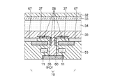
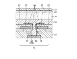
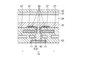
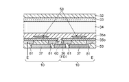
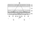
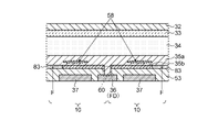
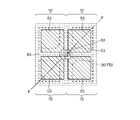
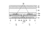
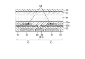
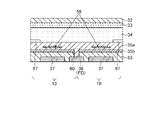
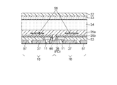
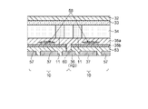
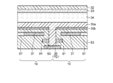
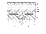
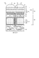
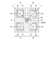
- FIG. 12 is a horizontal cross-sectional view showing still another example of the AA cross section in FIG. It is a vertical cross-sectional view which shows the cross-sectional structure of the pixel which concerns on the 2nd example of one Embodiment. It is a vertical cross-sectional view which shows the cross-sectional structure of the pixel which concerns on 3rd example of one Embodiment. It is a vertical cross-sectional view which shows the cross-sectional structure of the pixel which concerns on 4th example of one Embodiment. It is a vertical cross-sectional view which shows the cross-sectional structure of the pixel which concerns on 5th example of one Embodiment. 19 is a horizontal cross-sectional view showing a BB cross section in FIG.
- FIG. 22 is a horizontal cross-sectional view showing a CC cross section in FIG. 22. It is a vertical cross-sectional view which shows the cross-sectional structure of the pixel which concerns on 8th example of one Embodiment. It is a vertical cross-sectional view which shows the cross-sectional structure of the pixel which concerns on the 9th example of one Embodiment.
- FIG. 3 is a horizontal cross-sectional view showing a DD cross section in FIG. 31. It is a vertical cross-sectional view which shows the cross-sectional structure of the pixel which concerns on 15th example of one Embodiment. It is a vertical cross-sectional view which shows the cross-sectional structure of the pixel which concerns on 16th example of one Embodiment. It is a vertical cross-sectional view which shows the cross-sectional structure of the pixel which concerns on 17th example of one Embodiment.
- FIG. 11 is a horizontal cross-sectional view showing an EE cross section in FIG. 41. It is a vertical cross-sectional view which shows the cross-sectional structure of the pixel which concerns on the 23rd example of one Embodiment. It is a vertical cross-sectional view which shows the cross-sectional structure of the pixel which concerns on the 24th example of one Embodiment. It is a vertical cross-sectional view which shows the cross-sectional structure of the pixel which concerns on the 25th example of one Embodiment.
- FIG. 5 is a horizontal cross-sectional view showing an FF cross section in FIG. 45.
- FIG. 74 It is a vertical cross-sectional view which shows the cross-sectional structure of the image sensor which concerns on the 2nd variation of this disclosure.
- FIG. 7 is a horizontal cross-sectional view showing a cross section of II-II in FIG. 76.
- It is a block diagram which shows the structural example of one Embodiment of the image pickup apparatus as an electronic device to which this disclosure is applied.
- It is a block diagram which shows an example of the schematic structure of a vehicle control system.
- It is explanatory drawing which shows an example of the installation position of the vehicle exterior information detection unit and the image pickup unit.
- It is a figure which shows an example of the schematic structure of an endoscopic surgery system.
- CMOS Complementary Metal-Oxide Semiconductor
- CCD Charge-Coupled Device
- the CMOS type image sensor may be an image sensor created by applying or partially using a CMOS process.
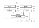
- FIG. 1 is a schematic diagram showing a schematic configuration example of an electronic device according to the present embodiment
- FIG. 2 is a schematic configuration example of a distance measuring device using the electronic device according to the present embodiment. It is a block diagram which shows.
- the electronic device 1 includes a laser light source 1010, an irradiation lens 1030, an image pickup lens 1040, an image sensor 100, and a system control unit 1050.
- the laser light source 1010 is composed of, for example, a vertical resonator type surface emitting laser (VCSEL) 1012 and a light source driving unit 1011 for driving the VCSEL 1012.
- VCSEL vertical resonator type surface emitting laser
- the present invention is not limited to VCSEL1012, and various light sources such as LEDs (Light Emitting Diode) may be used.
- the laser light source 1010 may be any of a point light source, a surface light source, and a line light source.
- the laser light source 1010 may include, for example, a configuration in which a plurality of point light sources (for example, VCSEL) are arranged one-dimensionally or two-dimensionally.
- the laser light source 1010 may emit light having a wavelength band different from that of visible light, such as infrared (IR) light.
- IR infrared
- the irradiation lens 1030 is arranged on the emission surface side of the laser light source 1010, and converts the light emitted from the laser light source 1010 into irradiation light having a predetermined spread angle.
- the image pickup lens 1040 is arranged on the light receiving surface side of the image sensor 100, and forms an image of incident light on the light receiving surface of the image sensor 100.
- the incident light may also include reflected light emitted from the laser light source 1010 and reflected by the subject 901.
- the image sensor 100 generates image data by driving a light receiving unit 1022 in which a plurality of pixels are arranged in a two-dimensional grid pattern and a light receiving unit 1022. It is composed of a sensor control unit 1021.
- the pixels arranged in the light receiving unit 1022 include, for example, a pixel for detecting light in a wavelength band of visible light, a pixel for detecting light in a wavelength band other than visible light, for example, a pixel for detecting light in a wavelength band of infrared light, and the like. It may be.
- the pixel that detects light in a wavelength band other than visible light may be a pixel (for an image sensor) for generating image data of light in a wavelength band other than visible light, or the distance to an object. It may be a pixel (for ToF sensor) for measuring, or a pixel (for EVS) for detecting a change in brightness.
- image data all the data read from each pixel of the light receiving unit 1022 and generated will be referred to as image data.
- the system control unit 1050 is configured by, for example, a processor (CPU), and drives the VCSEL 1012 via the light source drive unit 1011. Further, the system control unit 1050 acquires image data by controlling the image sensor 100. At that time, the system control unit 1050 controls the image sensor 100 in synchronization with the control for the laser light source 1010 to detect the reflected light of the irradiation light emitted from the laser light source 1010, and obtains image data. You may get it.
- a processor CPU
- the irradiation light emitted from the laser light source 1010 is projected onto the subject (also referred to as a measurement object or object) 901 through the irradiation lens 1030.
- This projected light is reflected by the subject 901.
- the light reflected by the subject 901 passes through the image pickup lens 1040 and is incident on the image sensor 100.
- the light receiving unit 1022 in the image sensor 100 receives the reflected light reflected by the subject 901 and generates image data.
- the image data generated by the image sensor 100 is supplied to the application processor 1100 of the electronic device 1.
- the application processor 1100 can execute various processes such as recognition processing and arithmetic processing on the image data input from the image sensor 100.
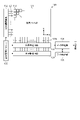
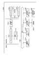
- FIG. 3 is a block diagram showing a schematic configuration example of an image sensor in the present embodiment.
- the image sensor 100 includes, for example, a pixel array unit 101, a vertical drive circuit 102, a signal processing circuit 103, a horizontal drive circuit 104, a system control circuit 105, and a data processing unit 108.
- a data storage unit 109 is provided.
- the vertical drive circuit 102, the signal processing circuit 103, the horizontal drive circuit 104, the system control circuit 105, the data processing unit 108, and the data storage unit 109 are also referred to as peripheral circuits.
- pixels (hereinafter referred to as unit pixels) 110 having a photoelectric conversion element that generates and stores electric charges according to the amount of received light are arranged in a row direction and a column direction, that is, in a two-dimensional lattice shape (hereinafter referred to as a two-dimensional lattice shape). It has a structure arranged in a matrix).
- the row direction means the arrangement direction of the pixels in the pixel row (in the drawing, the horizontal direction)
- the column direction means the arrangement direction of the pixels in the pixel row (in the drawing, the vertical direction).
- the pixel drive line LD is wired along the row direction for each pixel row and the vertical signal line VSL is wired along the column direction for each pixel row with respect to the matrix-shaped pixel array.
- the pixel drive line LD transmits a drive signal for driving when reading a signal from the pixel.
- the pixel drive lines LD are shown as wiring one by one, but the wiring is not limited to one by one.
- One end of the pixel drive line LD is connected to the output end corresponding to each line of the vertical drive circuit 102.
- the vertical drive circuit 102 is composed of a shift register, an address decoder, and the like, and drives each pixel of the pixel array unit 101 simultaneously for all pixels or in line units. That is, the vertical drive circuit 102 constitutes a drive unit that controls the operation of each pixel of the pixel array unit 101 together with the system control circuit 105 that controls the vertical drive circuit 102. Although the specific configuration of the vertical drive circuit 102 is not shown, it generally includes two scanning systems, a read scanning system and a sweep scanning system.
- the read scanning system selectively scans each pixel of the unit pixel 110 of the pixel array unit 101 row by row in order to read a signal from each pixel of the unit pixel 110.
- the signal read from each pixel of the unit pixel 110 is an analog signal.
- the sweep scan system performs sweep scan for the read row on which read scan is performed by the read scan system, ahead of the read scan by the exposure time.
- the photoelectric conversion element is reset by sweeping out unnecessary charges from the photoelectric conversion element of each pixel of the unit pixel 110 of the read row. Then, by sweeping out (resetting) unnecessary charges with this sweeping scanning system, a so-called electronic shutter operation is performed.
- the electronic shutter operation refers to an operation in which the electric charge of the photoelectric conversion element is discarded and a new exposure is started (charge accumulation is started).
- the signal read by the read operation by the read scanning system corresponds to the amount of light received after the read operation or the electronic shutter operation immediately before that.
- the period from the read timing by the immediately preceding read operation or the sweep timing by the electronic shutter operation to the read timing by the current read operation is the charge accumulation period (also referred to as an exposure period) in each pixel of the unit pixel 110.
- the signal output from each unit pixel 110 of the pixel row selectively scanned by the vertical drive circuit 102 is input to the signal processing circuit 103 through each of the vertical signal lines VSL for each pixel column.
- the signal processing circuit 103 performs predetermined signal processing on the signal output from each pixel of the selected row through the vertical signal line VSL for each pixel row of the pixel array unit 101, and temporarily processes the pixel signal after the signal processing. Hold on.
- the signal processing circuit 103 performs at least noise reduction processing, for example, CDS (Correlated Double Sampling) processing and DDS (Double Data Sampling) processing as signal processing.
- CDS Correlated Double Sampling
- DDS Double Data Sampling
- the CDS process removes pixel-specific fixed pattern noise such as reset noise and threshold variation of the amplification transistor in the pixel.
- the signal processing circuit 103 also has, for example, an AD (analog-digital) conversion function, and converts an analog pixel signal read from a photoelectric conversion element into a digital signal and outputs the signal.
- AD analog-digital
- the horizontal drive circuit 104 is composed of a shift register, an address decoder, and the like, and a read circuit (hereinafter referred to as a pixel circuit) corresponding to the pixel sequence of the signal processing circuit 103 is sequentially selected.
- a read circuit hereinafter referred to as a pixel circuit
- the system control circuit 105 is configured by a timing generator or the like that generates various timing signals, and based on the various timings generated by the timing generator, the vertical drive circuit 102, the signal processing circuit 103, and the horizontal drive circuit 104. Drive control such as.
- the data processing unit 108 has at least an arithmetic processing function, and performs various signal processing such as arithmetic processing on the pixel signal output from the signal processing circuit 103.
- the data storage unit 109 temporarily stores the data necessary for the signal processing in the data processing unit 108.
- the image data output from the data processing unit 108 may be, for example, executed by a predetermined process in the application processor 1100 or the like in the electronic device 1 equipped with the image sensor 100, or transmitted to the outside via a predetermined network. You may.
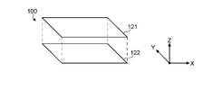
- FIG. 4 is a diagram showing an example of a laminated structure of an image sensor according to the present embodiment.
- the image sensor 100 has a stack structure in which a light receiving chip 121 and a circuit chip 122 are stacked one above the other.
- the light receiving chip 121 may be, for example, a semiconductor chip including a pixel array unit 101 in which a plurality of unit pixels 110 are arranged in a matrix
- the circuit chip 122 may be, for example, a semiconductor chip including the peripheral circuit in FIG. ..
- the bonding between the light receiving chip 121 and the circuit chip 122 for example, a so-called direct bonding in which the respective bonding surfaces are flattened and the two are bonded by an intramolecular force can be used.
- the present invention is not limited to this, and for example, so-called Cu-Cu bonding in which copper (Cu) electrode pads formed on the bonding surfaces of each other are bonded to each other, or other bump bonding or the like can be used. ..
- connection portion such as a TSV (Through-Silicon Via) that penetrates the semiconductor substrate.
- Connections using TSVs include, for example, a so-called twin TSV method in which two TSVs, a TSV provided on the light receiving chip 121 and a TSV provided from the light receiving chip 121 to the circuit chip 122, are connected on the outer surface of the chip, or a light receiving light.
- a so-called shared TSV method or the like, in which both are connected by a TSV penetrating from the chip 121 to the circuit chip 122, can be adopted.
- the unit pixel 110 is a pixel that detects each color component in the three primary colors of RGB (hereinafter, also referred to as RGB pixel 10) and a pixel that detects infrared (IR) light (hereinafter, also referred to as IR pixel 20).
- RGB pixel 10 a pixel that detects each color component in the three primary colors of RGB
- IR pixel 20 a pixel that detects infrared (IR) light
- IR pixel 20 a pixel that detects infrared (IR) light
- IR pixel 20 a pixel that detects infrared (IR) light
- IR pixel 20 infrared light
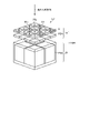
- FIG. 5 is a schematic diagram showing a schematic configuration example of the pixel array unit according to the present embodiment.
- unit pixels 110 having a structure in which unit pixels 110 composed of RGB pixels 10 and IR pixels 20 are arranged along the incident direction of light are arranged in a two-dimensional grid pattern. It has a configuration. That is, in the present embodiment, the RGB pixels 10 and the IR pixels 20 are located in the direction perpendicular to the arrangement direction (planar direction) of the unit pixels 110, and the RGB pixels 10 are located on the upstream side in the optical path of the incident light.
- the light transmitted through the image is configured to enter the IR pixel 20 located on the downstream side of the RGB pixel 10.
- the photoelectric conversion unit PD2 of the IR pixel 20 is arranged on the surface side opposite to the incident surface of the incident light in the photoelectric conversion unit PD1 of the RGB pixel 10.
- the optical axes of the incident light of the RGB pixels 10 and the IR pixels 20 arranged along the incident direction of the light are coincident or substantially the same.
- the photoelectric conversion unit PD1 constituting the RGB pixel 10 is composed of an organic material and the photoelectric conversion unit PD2 constituting the IR pixel 20 is composed of a semiconductor material such as silicon will be exemplified.
- both the photoelectric conversion unit PD1 and the photoelectric conversion unit PD2 may be made of a semiconductor material, or both the photoelectric conversion unit PD1 and the photoelectric conversion unit PD2 may be made of an organic material, or the photoelectric conversion unit may be made of an organic material.
- the part PD1 may be made of a semiconductor material, and the photoelectric conversion part PD2 may be made of an organic material.
- at least one of the photoelectric conversion unit PD1 and the photoelectric conversion unit PD2 may be made of a photoelectric conversion material different from the organic material and the semiconductor material.
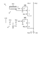
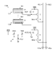
- FIG. 6 is a circuit diagram showing a schematic configuration example of a unit pixel according to the present embodiment. As shown in FIG. 6, in this example, the unit pixel 110 includes one RGB pixel 10 and one IR pixel 20.
- the RGB pixel 10 includes, for example, a photoelectric conversion unit PD1, a transfer gate 11, a floating diffusion region FD1, a reset transistor 12, an amplification transistor 13, and a selection transistor 14.
- the selection control line included in the pixel drive line LD is connected to the gate of the selection transistor 14, and the reset control line included in the pixel drive line LD is connected to the gate of the reset transistor 12, which will be described later.
- a transfer control line included in the pixel drive line LD is connected to the storage electrode (see the storage electrode 37 in FIG. 8 described later). Further, a vertical signal line VSL1 having one end connected to the signal processing circuit 103 is connected to the drain of the amplification transistor 13 via the selection transistor 14.
- the reset transistor 12, the amplification transistor 13, and the selection transistor 14 are collectively referred to as a pixel circuit.
- the pixel circuit may include a stray diffusion region FD1 and / or a transfer gate 11.
- the photoelectric conversion unit PD1 is made of, for example, an organic material, and performs photoelectric conversion of incident light.
- the transfer gate 11 transfers the electric charge generated in the photoelectric conversion unit PD1.
- the floating diffusion region FD1 accumulates the electric charge transferred by the transfer gate 11.
- the amplification transistor 13 causes a pixel signal having a voltage value corresponding to the electric charge stored in the stray diffusion region FD1 to appear on the vertical signal line VSL1.
- the reset transistor 12 emits the electric charge accumulated in the stray diffusion region FD1.
- the selection transistor 14 selects the RGB pixel 10 to be read.
- the anode of the photoelectric conversion unit PD1 is grounded, and the cascade is connected to the transfer gate 11.
- the details of the photoelectric conversion unit PD1 will be described later with reference to FIG. 8, but for example, the storage electrodes 37 are arranged close to each other.
- a voltage for collecting the electric charge generated in the photoelectric conversion unit PD1 in the semiconductor layer 35 in the vicinity of the storage electrode 37 is applied to the storage electrode 37 via the transfer control line.
- a voltage for causing the electric charge collected in the semiconductor layer 35 in the vicinity of the storage electrode 37 to flow out through the reading electrode 36 is applied to the storage electrode 37 via the transfer control line.
- the electric charge flowing out through the read electrode 36 is accumulated in the stray diffusion region FD1 configured by the wiring structure connecting the read electrode 36, the source of the reset transistor 12, and the gate of the amplification transistor 13.
- the drain of the reset transistor 12 may be connected to, for example, a power supply line to which a reset voltage lower than the power supply voltage VDD or the power supply voltage VDD is supplied.
- the source of the amplification transistor 13 may be connected to a power line via, for example, a constant current circuit (not shown).
- the drain of the amplification transistor 13 is connected to the source of the selection transistor 14, and the drain of the selection transistor 14 is connected to the vertical signal line VSL1.
- the floating diffusion region FD1 converts the accumulated electric charge into a voltage having a voltage value corresponding to the amount of the electric charge.
- the floating diffusion region FD1 may be, for example, a grounding capacitance.
- the present invention is not limited to this, and the floating diffusion region FD1 is added by intentionally connecting a capacitor or the like to a node to which the drain of the transfer gate 11 and the source of the reset transistor 12 and the gate of the amplification transistor 13 are connected. It may be a capacity or the like.
- the vertical signal line VSL1 is connected to an AD (Analog-to-Digital) conversion circuit 103a provided for each column (that is, for each vertical signal line VSL1) in the signal processing circuit 103.
- the AD conversion circuit 103a includes, for example, a comparator and a counter, and has a reference voltage such as a single slope or a lamp shape input from an external reference voltage generation circuit (DAC (Digital-to-Analog Converter)) and a vertical signal. By comparing with the pixel signal appearing on the line VSL1, the analog pixel signal is converted into the digital pixel signal.
- the AD conversion circuit 103a may be provided with, for example, a CDS (Correlated Double Sampling) circuit and may be configured to be able to reduce kTC noise and the like.
- the IR pixel 20 includes, for example, a photoelectric conversion unit PD2, a transfer transistor 21, a floating diffusion region FD2, a reset transistor 22, an amplification transistor 23, a selection transistor 24, and an emission transistor 25. That is, in the IR pixel 20, the transfer gate 11 in the RGB pixel 10 is replaced with the transfer transistor 21, and the emission transistor 25 is added.
- connection relationship between the stray diffusion region FD2, the reset transistor 22 and the amplification transistor 23 with respect to the transfer transistor 21 may be the same as the connection relationship between the stray diffusion region FD1, the reset transistor 12 and the amplification transistor 13 with respect to the transfer gate 11 in the RGB pixel 10. .. Further, the connection relationship between the amplification transistor 23, the selection transistor 24, and the vertical signal line VSL2 may be the same as the connection relationship between the amplification transistor 13 and the selection transistor 14 and the vertical signal line VSL1 in the RGB pixel 10.
- the source of the transfer transistor 21 is connected to, for example, the cathode of the photoelectric conversion unit PD2, and the drain is connected to the floating diffusion region FD2. Further, a transfer control line included in the pixel drive line LD is connected to the gate of the transfer transistor 21.
- the source of the emission transistor 25 may be connected to, for example, the cathode of the photoelectric conversion unit PD2, and the drain may be connected to a power supply line to which a reset voltage lower than the power supply voltage VDD or the power supply voltage VDD is supplied. Further, the emission control line included in the pixel drive line LD is connected to the gate of the emission transistor 25.
- the reset transistor 22, the amplification transistor 23, and the selection transistor 24 are collectively referred to as a pixel circuit.
- This pixel circuit may include one or more of the stray diffusion region FD2, the transfer transistor 21, and the emission transistor 25.
- the photoelectric conversion unit PD2 is made of, for example, a semiconductor material, and performs photoelectric conversion of incident light.
- the transfer transistor 21 transfers the electric charge generated in the photoelectric conversion unit PD2.
- the floating diffusion region FD2 accumulates the electric charge transferred by the transfer transistor 21.
- the amplification transistor 23 causes a pixel signal having a voltage value corresponding to the electric charge accumulated in the stray diffusion region FD2 to appear on the vertical signal line VSL2.
- the reset transistor 22 emits the electric charge accumulated in the stray diffusion region FD2.
- the selection transistor 24 selects the IR pixel 20 to be read.
- the anode of the photoelectric conversion unit PD2 is grounded, and the cascade is connected to the transfer transistor 21.
- the drain of the transfer transistor 21 is connected to the source of the reset transistor 22 and the gate of the amplification transistor 23, and the wiring structure connecting these constitutes the floating diffusion region FD2.
- the electric charge flowing out from the photoelectric conversion unit PD2 via the transfer transistor 21 is accumulated in the floating diffusion region FD2.
- the floating diffusion region FD2 converts the accumulated electric charge into a voltage having a voltage value corresponding to the amount of the electric charge.
- the floating diffusion region FD2 may be, for example, a grounding capacity.
- the present invention is not limited to this, and the stray diffusion region FD2 is added by intentionally connecting a capacitor or the like to a node to which the drain of the transfer transistor 21, the source of the reset transistor 22, and the gate of the amplification transistor 23 are connected. It may be a capacity or the like.
- the discharge transistor 25 is turned on when the charge accumulated in the photoelectric conversion unit PD2 is discharged and the photoelectric conversion unit PD2 is reset. As a result, the electric charge accumulated in the photoelectric conversion unit PD2 flows out to the power supply line via the discharge transistor 25, and the photoelectric conversion unit PD2 is reset to an unexposed state.
- the vertical signal line VSL2 is connected to the AD conversion circuit 103a provided for each column (that is, for each vertical signal line VSL2) in the IR signal processing circuit 103B.
- FIG. 7 is a circuit diagram showing a schematic configuration example of a unit pixel according to a modified example of the present embodiment. As shown in FIG. 7, in this modification, the RGB pixel 10A in each unit pixel 110 further includes a memory MEM and a transfer gate 15.
- the memory MEM is connected to the transfer gate 11 and temporarily holds the electric charge flowing out from the photoelectric conversion unit PD1.
- the transfer gate 15 is provided between the memory MEM and the stray diffusion region FD1 to suppress charge leakage from the memory MEM.
- the transfer gates 11 of all the RGB pixels 10 in the pixel array unit 101 are turned on all at once.
- the on state of the transfer gate 11 is a state configured in relation to the storage electrode 37.
- the potential of the storage electrode 37 is the potential of the transfer gate.
- the potential of the storage electrode 37 is lower than the potential of the transfer gate, so that the charge stored in the semiconductor layer 35 flows out to the FD1 via the transfer gate 11.
- the off state of the transfer gate 11 is, for example, when the electric charge generated in the photoelectric conversion unit PD1 is an electron, the potential of the storage electrode 37 is lower than the potential of the transfer gate 11, and the electric charge is a hole. It means that the electric charge generated in the photoelectric conversion film 34 is accumulated in the semiconductor layer 35 because the potential of the storage electrode 37 is higher than the potential of the transfer gate.
- the reading of the pixel signal based on the charge held in the memory MEM may be the same as the reading drive of the so-called rolling shutter method.
- the case where the electric charge generated by the photoelectric conversion units PD1 and PD2 by the photoelectric conversion is an electron is illustrated, but the present invention is not limited to this, and the direction of the potential control is reversed even when the charge is a hole.
- the technique according to the present disclosure can be applied in the same manner.
- FIG. 8 is a cross-sectional view showing an example of a cross-sectional structure of an image sensor according to the present embodiment.
- an example of the cross-sectional structure of the semiconductor chip in which the photoelectric conversion units PD1 and PD2 are formed in the unit pixel 110 will be described.
- a so-called back-illuminated cross-sectional structure in which the incident surface of light is the back surface side (opposite the element forming surface) of the semiconductor substrate 50 is exemplified, but the present invention is not limited to this, and the incident surface of light is incident. It may have a so-called surface-illuminated cross-sectional structure in which the surface is the surface side (element forming surface side) of the semiconductor substrate 50.
- the photoelectric conversion materials of the photoelectric conversion units PD1 and PD2 are organic materials and semiconductors. One or both of the materials (also referred to as inorganic materials) may be used.
- the image sensor 100 uses the same semiconductor substrate 50 for the photoelectric conversion unit PD1 and the photoelectric conversion unit PD2. It may have a built-in cross-sectional structure, or it may have a cross-sectional structure in which a semiconductor substrate in which the photoelectric conversion unit PD1 is built and a semiconductor substrate in which the photoelectric conversion unit PD2 is built are bonded together. Further, one of the photoelectric conversion units PD1 and PD2 may have a cross-sectional structure formed in the semiconductor substrate 50 and the other in the semiconductor layer formed on the back surface or the front surface of the semiconductor substrate 50. ..
- the photoelectric conversion unit PD2 of the IR pixel 20 is formed on the semiconductor substrate 50, and the RGB pixel 10 is formed on the back surface side (opposite the element forming surface) of the semiconductor substrate 50. It has a structure provided with the photoelectric conversion unit PD1 of the above.
- the back surface of the semiconductor substrate 50 is located on the upper side of the paper surface, and the front surface is located on the lower side.
- a semiconductor material such as silicon (Si) may be used.
- Si silicon
- the present invention is not limited to this, and various semiconductor materials including compound semiconductors such as GaAs, InGaAs, InP, AlGaAs, InGaP, AlGaInP, and InGaAsP may be used.
- the photoelectric conversion unit PD1 of the RGB pixel 10 is provided on the back surface side of the semiconductor substrate 50 with the insulating layer 53 interposed therebetween.
- the photoelectric conversion unit PD1 includes, for example, a photoelectric conversion film 34 made of an organic material, a transparent electrode 33 arranged so as to sandwich the photoelectric conversion film 34, and a semiconductor layer 35.
- the transparent electrode 33 provided on the upper side of the paper surface with respect to the photoelectric conversion film 34 (hereinafter, the upper side of the paper surface is the upper surface side and the lower side is the lower surface side) functions as, for example, the anode of the photoelectric conversion unit PD1.
- the semiconductor layer 35 provided on the lower surface side functions as a cathode of the photoelectric conversion unit PD1.
- the semiconductor layer 35 that functions as a cathode is electrically connected to the readout electrode 36 formed in the insulating layer 53.
- the readout electrode 36 is electrically drawn out to the surface (lower surface) side of the semiconductor substrate 50 by connecting to the wirings 61, 62, 63, and 64 penetrating the insulating layer 53 and the semiconductor substrate 50.
- the wiring 64 is electrically connected to the floating diffusion region FD1 shown in FIG.
- a storage electrode 37 is provided on the lower surface side of the semiconductor layer 35 that functions as a cathode with an insulating layer 53 interposed therebetween. Although not shown in FIG. 8, the storage electrode 37 is connected to the transfer control line in the pixel drive line LD1, and as described above, the charge generated in the photoelectric conversion unit PD1 at the time of exposure is stored in the storage electrode 37. A voltage for collecting the electric charge is applied to the semiconductor layer 35 in the vicinity, and at the time of reading, a voltage is applied for causing the electric charge collected in the semiconductor layer 35 in the vicinity of the storage electrode 37 to flow out through the reading electrode 36.
- the readout electrode 36 and the storage electrode 37 may be a transparent conductive film like the transparent electrode 33.
- a transparent conductive film such as indium tin oxide (ITO) or zinc oxide (IZO) may be used.
- ITO indium tin oxide
- IZO zinc oxide
- the present invention is not limited to these, and various conductive films may be used as long as they are conductive films capable of transmitting light in the wavelength band to be detected by the photoelectric conversion unit PD2.
- the semiconductor layer 35 for example, a transparent semiconductor layer such as IGZO may be used.
- IGZO a transparent semiconductor layer
- the present invention is not limited to these, and various semiconductor layers may be used as long as they are semiconductor layers capable of transmitting light in the wavelength band to be detected by the photoelectric conversion unit PD2.
- an insulating film such as a silicon oxide film (SiO 2 ) or a silicon nitride film (SiN) may be used.
- SiO 2 silicon oxide film
- SiN silicon nitride film
- the present invention is not limited to these, and various insulating films may be used as long as they can transmit light in the wavelength band to be detected by the photoelectric conversion unit PD2.
- a color filter 31 is provided on the upper surface side of the transparent electrode 33 that functions as an anode with a sealing film 32 interposed therebetween.
- the sealing film 32 is made of an insulating material such as silicon nitride (SiN), and these atoms are prevented from diffusing atoms such as aluminum (Al) and titanium (Ti) from the transparent electrode 33. May include.
- the color filters 31 will be described later. For example, for one RGB pixel 10, a color filter 31 that selectively transmits light having a specific wavelength component is provided. However, when a monochrome pixel for acquiring luminance information is provided instead of the RGB pixel 10 for acquiring color information, the color filter 31 may be omitted.
- the photoelectric conversion unit PD2 of the IR pixel 20 has, for example, a p-type semiconductor region 43 formed in the p-well region 42 of the semiconductor substrate 50 and an n-type semiconductor region 44 formed near the center of the p-type semiconductor region 43. Be prepared.
- the n-type semiconductor region 44 functions as, for example, a charge storage region for accumulating charges (electrons) generated by photoelectric conversion, and the p-type semiconductor region 43 collects charges generated by photoelectric conversion in the n-type semiconductor region 44. Functions as a region to form a potential gradient for.
- an IR filter 41 that selectively transmits IR light is arranged on the light incident surface side of the photoelectric conversion unit PD2.
- the IR filter 41 may be arranged, for example, in the insulating layer 53 provided on the back surface side of the semiconductor substrate 50.
- a fine uneven structure is provided on the light incident surface of the semiconductor substrate 50 in order to suppress the reflection of the incident light (IR light in this example).
- This uneven structure may be a so-called moth-eye structure, or may be a uneven structure having a different size and pitch from the moth-eye structure.
- a vertical transistor 45 that functions as a transfer transistor 21 is provided on the surface (lower surface of the paper surface) side of the semiconductor substrate 50, that is, on the element forming surface side.
- the gate electrode of the vertical transistor 45 reaches from the surface of the semiconductor substrate 50 to the n-type semiconductor region 44, and is a part of the wirings 65 and 66 (a part of the transfer control line of the pixel drive line LD2) formed in the interlayer insulating film 56. ) Is connected to the vertical drive circuit 102.
- the electric charge flowing out through the vertical transistor 45 is accumulated in the stray diffusion region FD2.
- the floating diffusion region FD2 is connected to the source of the reset transistor 22 and the gate of the amplification transistor 23 via a wiring (not shown) formed in the interlayer insulating film 56.
- the floating diffusion region FD2, the reset transistor 22, the amplification transistor 23, and the selection transistor 24 may be provided on the element forming surface of the semiconductor substrate 50, or may be provided on a semiconductor substrate different from the semiconductor substrate 50.
- the RGB pixel 10 located upstream with respect to the incident light generates an RGB image signal and the IR pixel 20 located downstream generates an image signal based on the IR light is illustrated. It is not limited to such a configuration.
- an image signal based on light having a wavelength component corresponding to green is generated by a pixel on the upstream side (corresponding to RGB pixel 10), and light having a wavelength component corresponding to red is generated by a pixel on the downstream side (corresponding to IR pixel 20). It may be configured to generate an image signal based on and an image signal based on light having a wavelength component corresponding to blue.
- a material that selectively absorbs the wavelength component corresponding to green is used for the photoelectric conversion film 34, and instead of the IR filter 41, a color filter that selectively transmits the wavelength component corresponding to red and blue are used.
- Color filters that selectively transmit the corresponding wavelength components can be arranged in a matrix. Further, in this configuration, it is possible to omit the color filter 31. With such a configuration, it is possible to expand the light receiving area of the pixel that detects the wavelength component of each of the three RGB primary colors (which may be CMY three primary colors) constituting the color image, so that the quantum efficiency is increased. It is possible to achieve an improvement in the S / N ratio.
- the semiconductor substrate 50 is provided with a pixel separation unit 54 that electrically separates between a plurality of unit pixels 110, and a photoelectric conversion unit PD2 is provided in each region partitioned by the pixel separation unit 54. ..
- the pixel separation unit 54 has, for example, a grid shape interposed between a plurality of unit pixels 110, and each photoelectric.
- the conversion unit PD2 is formed in each region partitioned by the pixel separation unit 54.
- a reflective film that reflects light such as tungsten (W) or aluminum (Al) may be used.
- the incident light that has entered the photoelectric conversion unit PD2 can be reflected by the pixel separation unit 54, so that the optical path length of the incident light in the photoelectric conversion unit PD2 can be lengthened.
- the pixel separation unit 54 by forming the pixel separation unit 54 with a light reflection structure, it is possible to reduce leakage of light to adjacent pixels, so that it is possible to further improve image quality, distance measurement accuracy, and the like.
- the configuration in which the pixel separation unit 54 has a light reflection structure is not limited to the configuration using a reflective film, and can be realized, for example, by using a material having a refractive index different from that of the semiconductor substrate 50 for the pixel separation unit 54. can.
- a fixed charge film 55 is provided between the semiconductor substrate 50 and the pixel separation unit 54.
- the fixed charge film 55 uses, for example, a high dielectric having a negative fixed charge so that a positive charge (hole) storage region is formed at the interface with the semiconductor substrate 50 and the generation of dark current is suppressed. It is formed. Since the fixed charge film 55 is formed so as to have a negative fixed charge, an electric field is applied to the interface with the semiconductor substrate 138 due to the negative fixed charge, and a positive charge (hole) storage region is formed.
- the fixed charge film 55 can be formed of, for example, a hafnium oxide film (HfO 2 film). Further, the fixed charge film 55 can be formed so as to contain at least one of other oxides such as hafnium, zirconium, aluminum, tantalum, titanium, magnesium, yttrium, and lanthanoid element.
- hafnium oxide film HfO 2 film
- other oxides such as hafnium, zirconium, aluminum, tantalum, titanium, magnesium, yttrium, and lanthanoid element.
- FIG. 8 illustrates a case where the pixel separating portion 54 has a so-called FTI (Full Trench Isolation) structure in which the pixel separating portion 54 reaches from the front surface to the back surface of the semiconductor substrate 50, but the present invention is not limited to this, and for example, pixels. It is possible to adopt various element separation structures such as a so-called DTI (Deep Trench Isolation) structure in which the separation portion 54 is formed from the back surface or the front surface of the semiconductor substrate 50 to the vicinity of the middle part of the semiconductor substrate 50.
- FTI Frull Trench Isolation
- the upper surface of the flattening film 52 is flattened by, for example, CMP (Chemical Mechanical Polishing), and an on-chip lens 51 for each unit pixel 110 is provided on the flattened upper surface.
- the on-chip lens 51 of each unit pixel 110 has a curvature that collects incident light on the photoelectric conversion units PD1 and PD2.
- the positional relationship between the on-chip lens 51, the color filter 31, the IR filter 41, and the photoelectric conversion unit PD2 in each unit pixel 110 is adjusted according to, for example, the distance (image height) from the center of the pixel array unit 101. May (pupil correction).
- a light-shielding film may be provided to prevent light incident obliquely from leaking to adjacent pixels.
- the light-shielding film may be located above the pixel separation portion 54 provided inside the semiconductor substrate 50 (upstream side in the optical path of the incident light).
- the position of the light-shielding film may be adjusted according to, for example, the distance (image height) from the center of the pixel array unit 101.
- Such a light-shielding film may be provided in, for example, the sealing film 32 or the flattening film 52.
- a light-shielding material such as aluminum (Al) or tungsten (W) may be used as the material of the light-shielding film.
- the layer structure of the photoelectric conversion film 34 can be as follows. However, in the case of a laminated structure, the stacking order can be changed as appropriate.
- (1) Single-layer structure of p-type organic semiconductor (2) Single-layer structure of n-type organic semiconductor (3-1) Laminated structure of p-type organic semiconductor layer / n-type organic semiconductor layer (3-2) p-type organic semiconductor Layer / Mixed layer of p-type organic semiconductor and n-type organic semiconductor (bulk heterostructure) / Laminated structure of n-type organic semiconductor layer (3-3) p-type organic semiconductor layer / p-type organic semiconductor and n-type organic semiconductor Laminated structure of mixed layer (bulk heterostructure) (3-4) Laminated structure of n-type organic semiconductor layer / mixed layer of p-type organic semiconductor and n-type organic semiconductor (bulk heterostructure) (4) p-type organic semiconductor and p-type Mixed layer with organic semiconductor (
- n-type organic semiconductor examples include fullerenes and fullerene derivatives (for example, fullerenes such as C60, C70 and C74 (higher-order fullerenes, encapsulated fullerenes, etc.) or fullerenes derivatives (eg, fullerene fluorides, PCBM fullerene compounds, fullerene multimers, etc.).
- fullerenes and fullerene derivatives for example, fullerenes such as C60, C70 and C74 (higher-order fullerenes, encapsulated fullerenes, etc.) or fullerenes derivatives (eg, fullerene fluorides, PCBM fullerene compounds, fullerene multimers, etc.).
- fullerenes and fullerene derivatives for example, fullerenes such as C60, C70 and C74 (higher-order fullerenes, encapsulated fullerenes, etc.) or fuller
- n-type organic semiconductor examples include heterocyclic compounds containing a nitrogen atom, an oxygen atom, and a sulfur atom, such as a pyridine derivative, a pyrazine derivative, a pyrimidine derivative, a triazine derivative, a quinoline derivative, a quinoxalin derivative, an isoquinolin derivative, and an acridin.
- Derivatives phenazine derivatives, phenanthroline derivatives, tetrazole derivatives, pyrazole derivatives, imidazole derivatives, thiazole derivatives, oxazole derivatives, imidazole derivatives, benzimidazole derivatives, benzotriazole derivatives, benzoxazole derivatives, benzoxazole derivatives, carbazole derivatives, benzofuran derivatives, dibenzofuran derivatives , Subporphyrazine derivative, polyphenylene vinylene derivative, polybenzothianazole derivative, polyfluorene derivative and the like as a part of the molecular skeleton, organic molecule, organic metal complex and subphthalocyanine derivative can be mentioned.
- Examples of the group contained in the fullerene derivative include a halogen atom; a linear, branched or cyclic alkyl group or phenyl group; a group having a linear or condensed aromatic compound; a group having a halide; a partial fluoroalkyl group; Fluoroalkyl group; silylalkyl group; silylalkoxy group; arylsilyl group;arylsulfanyl group;alkylsulfanyl group;arylsulfonyl group;alkylsulfonyl group;arylsulfide group;alkylsulfide group;amino group;alkylamino group;arylamino group Hydroxy group; alkoxy group; acylamino group; acyloxy group; carbonyl group; carboxy group; carboxoamide group; carboalkoxy group; acyl group; sulfonyl group; cyano group; nitro group; group having
- the film thickness of the photoelectric conversion film 34 made of the above organic materials is not limited to the following values, but is, for example, 1 ⁇ 10-8 m (meters) to 5 ⁇ 10-7 . m, preferably 2.5 ⁇ 10 -8 m to 3 ⁇ 10 -7 m, more preferably 2.5 ⁇ 10 -8 m to 2 ⁇ 10 -7 m, and even more preferably 1 ⁇ 10 -7 . M to 1.8 ⁇ 10-7 m can be exemplified.
- Organic semiconductors are often classified into p-type and n-type, but p-type means that holes are easily transported, and n-type means that electrons are easily transported, and they are inorganic. It is not limited to the interpretation that it has holes or electrons as a majority carrier of thermal excitation like a semiconductor.
- Examples of the material constituting the photoelectric conversion film 34 that photoelectrically converts light having a green wavelength include rhodamine-based dyes, melancyanine-based dyes, quinacridone derivatives, subphthalocyanine-based dyes (subphthalocyanine derivatives), and the like.
- examples of the material constituting the photoelectric conversion film 34 for photoelectric conversion of blue light include coumalic acid dye, tris-8-hydroxyquinolialuminum (Alq3), and melanin-based dye.
- examples of the material constituting the photoelectric conversion film 34 for photoelectric conversion of red light include a phthalocyanine dye and a subphthalocyanine dye (subphthalocyanine derivative).
- the photoelectric conversion film 34 it is also possible to use a panchromatic photosensitive organic photoelectric conversion film that is sensitive to almost all visible light from the ultraviolet region to the red region.
- the material constituting the semiconductor layer 35 has a large bandgap value (for example, a bandgap value of 3.0 eV (electron volt) or more), and the mobility is higher than that of the material constituting the photoelectric conversion film 34. It is preferable that a material having a degree is used. Specific examples thereof include oxide semiconductor materials such as IGZO, transition metal dichalcogenides, silicon carbides, diamonds, graphene, carbon nanotubes, and organic semiconductor materials such as condensed polycyclic hydrocarbon compounds and condensed heterocyclic compounds. ..
- the charge generated in the photoelectric conversion film 34 is an electron
- a material having an ionization potential larger than that of the material constituting the photoelectric conversion film 34 can be used as the material constituting the semiconductor layer 35.
- the charge is a hole
- a material having an electron affinity smaller than that of the material constituting the photoelectric conversion film 34 can be used as the material constituting the semiconductor layer 35.
- the impurity concentration in the material constituting the semiconductor layer 35 is preferably 1 ⁇ 10 18 cm -3 or less. Further, if the photoelectric conversion performance and the mobility performance can be satisfied, the photoelectric conversion film 34 and the semiconductor layer 35 can be made of the same material.
- a transparent material is used for each of the transparent electrode 33, the readout electrode 36, the semiconductor layer 35, and the storage electrode 37.
- a material composed of Al-Nd (alloy of aluminum and neodymium) or ASC (alloy of aluminum, samarium and copper) can be used.
- the bandgap energy of the transparent conductive material is 2.5 eV or more, preferably 3.1 eV or more.
- the transparent conductive material constituting them may be a conductive metal oxide.
- indium oxide indium-tin oxide (including ITO (Indium Tin Oxide), Sn-doped In 2 O 3 , crystalline ITO and amorphous ITO), and indium-zinc oxide added with indium as a dopant.
- ITO Indium Tin Oxide
- IGO indium-gallium oxide
- IGZO indium-gallium-zinc oxide
- indium-tin-zinc oxide indium-tin-zinc oxide (ITZO) in which indium and tin are added as dopants to zinc oxide
- IFO F-doped In 2 O 3
- tin oxide SnO 2
- ATO Sb-doped SnO 2
- FTO F-doped SnO 2
- zinc oxide including ZnO doped with other elements
- aluminum-zinc oxide AZO in which aluminum is added as a dopant to zinc oxide, and zinc oxide.
- Gallium-zinc oxide with gallium added as a dopant, titanium oxide (TiO 2 ), niobium-titanium oxide (TNO) with niobium added as a dopant to titanium oxide, antimony oxide, spinel-type oxide, YbFe 2
- GZO gallium-zinc oxide
- TiO 2 titanium oxide
- TNO niobium-titanium oxide
- O4 YbFe 2
- a transparent electrode having a gallium oxide, titanium oxide, niobium oxide, nickel oxide or the like as a base layer can be mentioned.
- the thickness of the transparent electrode 2 ⁇ 10 -8 m to 2 ⁇ 10 -7 m, preferably 3 ⁇ 10 -8 m to 1 ⁇ 10 -7 m can be mentioned.
- each unit pixel 110 may include N (N is an integer of 1 or more) RGB pixels 10 and M (M is an integer of 1 or more) IR pixels 20.
- N RGB pixels 10 may share a part of the pixel circuit
- M IR pixels 20 may share a part of the pixel circuit.
- FIG. 9 is a schematic diagram showing a schematic configuration example of a unit pixel according to a modification of the present embodiment.
- the unit pixel 110A has a structure in which one IR pixel 20 is arranged in the incident direction of light for four RGB pixels 10 arranged in 2 rows and 2 columns. That is, in this modification, one IR pixel 20 for each of the four RGB pixels 10 is located in the direction perpendicular to the arrangement direction (planar direction) of the unit pixels 110A, and is on the upstream side in the optical path of the incident light.
- the light transmitted through the four RGB pixels 10 located in is incident on one IR pixel 20 located on the downstream side of the four RGB pixels 10. Therefore, in this modification, the optical axis of the incident light of the IR pixel 20 and the unit array of the Bayer array composed of the four RGB pixels 10 are coincident or substantially the same.
- FIG. 10 is a circuit diagram showing a schematic configuration example of a unit pixel according to a modification of the present embodiment.
- the unit pixel 110A includes a plurality of RGB pixels 10-1 to 10-N (N is 4 in FIG. 10) and one IR pixel 20.
- the plurality of RGB pixels 10 share one pixel circuit (reset transistor 12, stray diffusion region FD1, amplification transistor 13 and selection transistor 14). It is possible (pixel sharing).
- a plurality of RGB pixels 10-1 to 10-N share a pixel circuit including a reset transistor 12, a stray diffusion region FD1, an amplification transistor 13, and a selection transistor 14. That is, in this modification, a plurality of photoelectric conversion units PD1 and transfer gate 11 are connected to the common floating diffusion region FD1.
- FIG. 11 is a cross-sectional view showing an example of a cross-sectional structure of an image sensor according to a modified example of the present embodiment.
- each unit pixel 110A is composed of four RGB pixels 10 arranged in two rows and two columns and one IR pixel 20
- an example of the cross-sectional structure of the semiconductor chip in which the photoelectric conversion units PD1 and PD2 are formed in the unit pixel 110A will be described.
- the duplicated description will be omitted by quoting them.
- the on-chip lens 51, the color filter 31, and the storage electrode 37 are four in two rows and two columns. (However, two of the four are shown in FIG. 11), thereby forming four RGB pixels 10.
- the four RGB pixels 10 in each unit pixel 210 may form a basic array of Bayer arrays.
- the RGB pixel 10 is also simply referred to as a pixel 10.
- the readout electrode 36 electrically connected to the floating diffusion region FD1 will be described as a part of the floating diffusion region FD1.
- the electric charge generated by the photoelectric conversion film 34 is a negative charge (that is, an electron) is illustrated.
- the electric charge generated by the photoelectric conversion film 34 may be a positive charge (that is, a hole).
- the structures and effects described in each example may be similar to other examples unless otherwise noted.
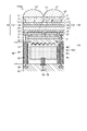
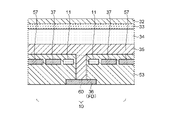
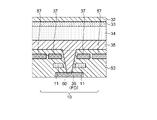
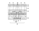
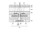
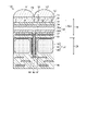
- FIG. 12 is a vertical cross-sectional view showing a cross-sectional structure of a pixel according to the first example of the present embodiment.
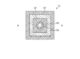
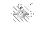
- FIG. 13 is a horizontal cross-sectional view showing a cross section taken along the line AA in FIG.
- the term "perpendicular” here means that the semiconductor substrate 50 is perpendicular to the element forming surface, and the term “horizontal” means that the semiconductor substrate 50 is horizontal to the element forming surface.
- this protruding portion is referred to as a semiconductor wiring 60.
- a storage electrode 37 having an open center is arranged so as to surround the semiconductor wiring 60.
- An insulating layer 53 is interposed between the storage electrode 37 and the semiconductor wiring 60 to electrically separate them.
- a transfer gate 11 is arranged on the read electrode 36 side of the semiconductor wiring 60.
- the transfer gate 11 is composed of, for example, a fixed charge film having the same polarity as the charge generated by the photoelectric conversion film 34.
- a hafnium oxide film (HfO 2 film) and other oxides such as hafnium, zirconium, aluminum, tantalum, titanium, magnesium, yttrium, and lanthanoid elements are used. Can be formed to include at least one of.
- the potential of the fixed charge film, that is, the transfer gate 11 is lower than the potential of the semiconductor layer 35 in the vicinity of the storage electrode 37 when the storage electrode 37 is turned off. Similar to the storage electrode 37, such a transfer gate 11 has a shape with an opening in the center and is arranged so as to surround the semiconductor wiring 60.
- the transfer gate 11 and the semiconductor wiring 60 may be separated or contact with each other via the insulating layer 53.
- the storage electrode 37 and the transfer gate 11 arranged with respect to the semiconductor wiring 60 are for each pixel 10. It may be divided into.
- a drive signal (also referred to as a control voltage) for lowering the potential in the semiconductor layer 35 in the vicinity of the storage electrode 37 is applied to the storage electrode 37 from the vertical drive circuit 102. Therefore, the electric charge 58 generated in the photoelectric conversion film 34 and entering the semiconductor layer 35 accumulates in the region near the storage electrode 37 in the semiconductor layer 35. At that time, since the transfer gate 11 having the same polarity as the electric charge forms a potential barrier in the semiconductor wiring 60 between the region where the electric charge is accumulated and the transfer gate 11, the read electrode 36 side of the accumulated electric charge is formed. Leakage to is suppressed. Thereby, it becomes possible to improve the quantum efficiency.
- the shield electrode (SLD) 57 is arranged so as to surround the storage electrode (ASE) 37 of each pixel 10.
- the shield electrode 57 is connected to the vertical drive circuit 102 via a wiring (not shown) which is one of the pixel drive lines LD.
- the vertical drive circuit 102 drives each pixel 10 individually, the vertical drive circuit 102 applies a drive signal to the shield electrode 57 to form a potential barrier in the semiconductor layer 35 located between the adjacent pixels 10.
- the charge generated in the photoelectric conversion film 34 of a certain pixel 10 and entering the semiconductor layer 35 is suppressed from flowing out to the adjacent pixel 10, so that the quantum efficiency of the pixel 10 can be further improved.
- FIG. 13 illustrates a case where the horizontal cross section of the semiconductor wiring 60 and the opening shapes of the storage electrode 37 and the transfer gate 11 are circular.
- a quadrangle, a regular octagon, or the like is illustrated. It may be changed to various shapes such as polygons and ellipses. This also applies to other examples described later.
- FIG. 16 is a vertical cross-sectional view showing a cross-sectional structure of a pixel according to the second example of the present embodiment.
- the pixel 10 according to the second example has the same cross-sectional structure as the pixel 10 according to the first example described above with reference to FIG. 12, and the transfer gate 11 is arranged inside the storage electrode 37. It has a structure that has been constructed. That is, in the second example, the opening of the storage electrode 37 is enlarged in diameter, and the transfer gate 11 is arranged on the same plane as the storage electrode 37.
- the length of the semiconductor wiring 60 can be shortened, so that the height of the image sensor 100 can be reduced, and the size of the image sensor 100 can be reduced.
- FIG. 17 is a vertical cross-sectional view showing a cross-sectional structure of a pixel according to the third example of the present embodiment.
- the pixel 10 according to the third example has the same cross-sectional structure as the pixel 10 according to the first example described above with reference to FIG. 12, as the semiconductor wiring 60 approaches the readout electrode 36. It has a tapered shape that becomes thinner.
- the diameter of the semiconductor wiring 60 on the readout electrode 36 side is narrowed, the contact area with the readout electrode 36 is reduced, whereby the readout electrode 36 can be reduced. As a result, it is possible to increase the amount of light propagating to the lower layer than the readout electrode 36. Therefore, for example, the quantum of the IR pixel 20 when the photoelectric conversion unit PD2 of the IR pixel 20 is arranged in the lower layer of the pixel 10. It is possible to increase the efficiency.
- FIG. 18 is a vertical cross-sectional view showing a cross-sectional structure of a pixel according to the fourth example of the present embodiment.
- the pixel 10 according to the fourth example has a cross-sectional structure similar to that of the pixel 10 according to the first example described above with reference to FIG. It has a structure in which the floating diffusion region FD) is shared.
- the read electrode 36 and the floating diffusion region FD are shared and the transfer of electric charges from each pixel 10 to the floating diffusion region FD can be controlled by using the transfer gate 11, the reading for each pixel 10 is possible. And simultaneous reading from a plurality of pixels 10 can be switched.
- FIG. 19 is a vertical cross-sectional view showing a cross-sectional structure of a pixel according to the fifth example of the present embodiment.
- FIG. 20 is a horizontal cross-sectional view showing a BB cross section in FIG. Note that FIG. 19 shows the configuration of the upper layer from the color filter 31 for convenience of explanation.
- the pixel 10 according to the fifth example has a plurality of (two in this example) in the same cross-sectional structure as the pixel 10 according to the first example described above with reference to FIG. It has a structure in which one on-chip lens 51 is provided for the pixel 10 of the above.
- FIG. 21 is a vertical cross-sectional view showing a cross-sectional structure of a pixel according to a sixth example of the present embodiment.
- the pixel 10 according to the sixth example has the same cross-sectional structure as the pixel 10 according to the first example described above with reference to FIG. 12, between the transfer gate 11 and the read electrode 36.
- the memory electrode 16 constituting the memory MEM and the transfer gate 15 are arranged in order.
- the transfer gate 15 is composed of a fixed charge film and is arranged on the side closest to the read electrode 36 in the semiconductor wiring 60. However, the potential of the transfer gate 15 may be lower than the potential of the transfer gate 11. Similar to the storage electrode 37, the transfer gate 15 has a shape with an opening in the center and is arranged so as to surround the semiconductor wiring 60. The transfer gate 15 and the semiconductor wiring 60 may be separated from each other via the insulating layer 53 or may be in contact with each other.
- the memory electrode 16 is arranged between the transfer gate 11 and the transfer gate 15. Further, the memory electrode 16 has a shape with an opening in the center like the storage electrode 37, and is arranged so as to surround the semiconductor wiring 60.
- the electric charge transferred from the semiconductor layer 35 via the transfer gate 11 can be temporarily held in the region near the memory electrode 16 in the semiconductor wiring 60. As a result, the reading drive of the global shutter method becomes possible.
- FIG. 22 is a vertical cross-sectional view showing a cross-sectional structure of a pixel according to a seventh example of the present embodiment.
- FIG. 23 is a horizontal cross-sectional view showing a CC cross section in FIG. 22.
- the transfer gate 11 in all the pixels 10, that is, the storage electrode 37 is driven at the same time. Therefore, as shown in FIGS. 22 and 23, the storage electrodes 37 of all the pixels 10 in the pixel array unit 101 may be connected by the wiring 73. Similarly, the memory electrodes 16 of all the pixels 10 in the pixel array unit 101 may also be connected by the wiring 72.
- FIG. 24 is a vertical cross-sectional view showing a cross-sectional structure of a pixel according to an eighth example of the present embodiment.
- the pixel 10 according to the eighth example has the same cross-sectional structure as the pixel 10 according to the sixth example described above with reference to FIG. 21, and the semiconductor layer 35 is the first semiconductor layer 35A and the first semiconductor layer 35A. It has a structure divided into two layers, that is, two semiconductor layers 35B. An insulating layer 53 is interposed between the first semiconductor layer 35A and the second semiconductor layer 35B. The semiconductor wiring 60 penetrates from the first semiconductor layer 35A to the second semiconductor layer 35B and reaches the readout electrode 36.
- the storage electrode 37, the transfer gate 11, and the shield electrode 57 are arranged in the insulating layer 53 between the first semiconductor layer 35A and the second semiconductor layer 35B, as in the sixth example.
- the memory electrode 16 and the transfer gate 15 are arranged in the insulating layer 53 between the second semiconductor layer 35B and the read electrode 36. More specifically, the memory electrode 16 is arranged on the second semiconductor layer 35B side in the semiconductor wiring 60 between the second semiconductor layer 35B and the read electrode 36, and the transfer gate 15 reads out from the second semiconductor layer 35B. It is arranged on the read electrode 36 side in the semiconductor wiring 60 between the electrode 36 and the semiconductor wiring 60.
- a shield electrode 57B similar to the shield electrode 57 is provided.
- the shield electrode 57B is connected to the vertical drive circuit 102 via a wiring (not shown) which is one of the pixel drive lines LD.
- the vertical drive circuit 102 drives each pixel 10 individually, the vertical drive circuit 102 applies a drive signal to the shield electrode 57 to form a potential barrier in the second semiconductor layer 35B located between the adjacent pixels 10.
- the electric charge held in the memory MEM of a certain pixel 10 is suppressed from flowing out to the memory MEM of the adjacent pixel 10, so that the quantum efficiency of the pixel 10 can be further improved.
- Example 9 a driving example of the global shutter system will be described.
- the driving example of the pixel 10 described with reference to FIG. 21 in the sixth example will be described, but the driving is not limited to this, and the driving of the global shutter method (hereinafter referred to as the global shutter driving) is possible. The same can be applied to the example of.
- FIG. 25 is a vertical cross-sectional view showing a cross-sectional structure of a pixel according to a ninth example of the present embodiment.
- the exposure operation is performed on the other pixel 10 while one of the two adjacent pixels 10a and 10b is executing the exposure operation. Not executed.
- the two pixels 10a and 10b may have the same configuration as the above-mentioned pixel 10, respectively.
- the storage electrode 37 of the pixel 10b is turned on and the storage electrode 37 of the pixel 10a is turned off. Further, the shield electrode 57 located between these two pixels 10a and 10b is turned off. In this state, the transfer gate 11 and the transfer gate 15 of the pixel 10a, and the transfer gate 11, the memory electrode 16 and the transfer gate 15 of the pixel 10b are turned off. Further, the memory electrode 16 of the pixel 10a is turned on.
- the on state of the storage electrode 37, the shield electrode 57, and the memory electrode 16 means a state in which a drive signal is supplied to each electrode from the vertical drive circuit 102, and an off state means a drive signal from the vertical drive circuit 102. Is not supplied.
- the electric charge 58 generated in the photoelectric conversion film 34 corresponding to the photoelectric conversion unit PD1 of each of the pixels 10a and 10b is attracted to the storage electrode 37 of the pixel 10b, and thereby the electric charge generated in the photoelectric conversion film 34. 58 is accumulated in the semiconductor layer 35 in the vicinity of the storage electrode 37 in the pixel 10b.
- the outflow destination of the charge 58 overflowing from the semiconductor layer 35 in the vicinity of the storage electrode 37 in the pixel 10b may be the floating diffusion region FD connected to the read electrode 36 of the pixel 10b.
- the charge 59 stored in the semiconductor layer 35 near the storage electrode 37 in the front frame is held in the memory MEM.
- the charges 59 stored in the memory MEM are sequentially read out by the read operation for the pixel 10a executed in parallel during the exposure to the pixel 10b, and are used for generating the pixel signal.
- FIG. 26 is a vertical cross-sectional view showing a cross-sectional structure of a pixel according to a tenth example of the present embodiment.
- the shield electrode 57 located between the two pixels 10a and 10b forming the pair was turned off while the global shutter drive was being executed.
- the shield electrode 57 between the two pixels 10a and 10b forming the pair is omitted.
- the configuration for driving the shield electrode 57 can be omitted, so that the size can be reduced by omitting the pixel drive line LD for driving the shield electrode 57 and the shield electrode 57, and the power consumption during driving the global shutter can be reduced. The effect of is obtained.
- FIG. 27 is a vertical cross-sectional view showing a cross-sectional structure of a pixel according to the eleventh example of the present embodiment.
- the read electrode 36 and the floating diffusion region FD of the two pixels 10a and 10b forming the pair are shared.
- the global shutter drive can be realized by the drive described in the ninth example.
- FIG. 28 is a vertical cross-sectional view showing an example of a cross-sectional structure of a pixel according to the twelfth example of the present embodiment.
- the semiconductor layer 35 (including the first semiconductor layer 35A and the second semiconductor layer 35B described in the eighth example) in each of the above-mentioned and later examples includes the first layer 35a and the second layer 35b. It may be composed of two layers of.
- the second layer 35b is provided, for example, on a surface of the semiconductor layer 35 that comes into contact with the insulating layer 53.
- the second layer 35b may be a film provided for the purpose of reducing the interface trap level formed between the insulating layer 53 and the first layer 35a. Further, as the material constituting each of the first layer 35a and the second layer 35b, for example, the same material as the above-mentioned semiconductor layer 35 may be used. However, the first layer 35a and the second layer 35b may have different properties, for example, due to differences in composition and the like.
- the second layer 35b for reducing the interface trap level between the insulating layer 53 and the first layer 35a, it is formed between the insulating layer 53 and the first layer 35a. Since the interface trap level is reduced, it is possible to reduce the afterimage generated between the frames.
- the color filter 31 may be arranged on the incident surface side (on-chip lens 51 side) of light with respect to the photoelectric conversion film 34, as illustrated in FIG. 29, or in FIG. 30. As illustrated in the above, it may be arranged on the side opposite to the incident surface of light (on the circuit chip 122 side (not shown)) with respect to the photoelectric conversion film 34.
- the color filter 31 When the color filter 31 is arranged on the side opposite to the incident surface of light from the photoelectric conversion film 34, the color filter 31 may be arranged in the insulating layer 53, for example, as illustrated in FIG.
- the shield electrode 57 (and the shield electrode 57B) are arranged between the pixels 10 in order to prevent charge leakage (blooming) between the pixels 10.
- the 14th example by arranging a fixed charge film having the same polarity as the charge between the pixels 10 instead of the shield electrode 57 (and the shield electrode 57B), the charge leaks between the pixels 10.
- a configuration for preventing (blooming) will be described.
- the base pixel 10 is not limited to the pixel 10 according to the first example, and is the pixel 10 according to another example. You may.
- FIG. 31 is a vertical cross-sectional view showing the cross-sectional structure of the pixel according to the 14th example of the present embodiment.
- FIG. 32 is a horizontal cross-sectional view showing a DD cross section in FIG. 31.
- the shield charge film 67 may be composed of a fixed charge film having the same polarity as the charge generated by the photoelectric conversion film 34.
- the shield charge film 67 is arranged on the same surface as the surface on which the storage electrode 37 is arranged.
- the shield charge film 67 may be in contact with the side surface of the storage electrode 37 or may be separated from the side surface of the storage electrode 37.
- the size can be reduced by omitting the shield electrode 57 and the pixel drive line LD for driving the shield electrode 57.
- the storage electrode 37 can be expanded. As a result, electric charges can be efficiently collected by the semiconductor layer 35 in the vicinity of the storage electrode 37, and further improvement in quantum efficiency can be expected.
- FIG. 33 is a vertical cross-sectional view showing a cross-sectional structure of a pixel according to the fifteenth example of the present embodiment.
- the shield charge film 67 is a boundary portion between adjacent pixels 10, and is a surface of the insulating layer 53 on which the upper surface of the storage electrode 37 is arranged and the semiconductor layer 35 (other than the semiconductor wiring 60). It may be arranged between the lower surface and the lower surface. At that time, the region around the opening in the shielded charge film 67 may be superimposed on the outer peripheral portion of the storage electrode 37 in the vertical direction.
- FIG. 34 is a vertical cross-sectional view showing a cross-sectional structure of a pixel according to the 16th example of the present embodiment.
- the shield charge film 67 may be arranged at a boundary portion between adjacent pixels 10 and in a lower layer portion of the semiconductor layer 35, that is, a region in contact with the insulating layer 53 in the semiconductor layer 35. At that time, the region around the opening in the shielded charge film 67 may be superimposed on the outer peripheral portion of the storage electrode 37 in the vertical direction.
- FIG. 35 is a vertical cross-sectional view showing a cross-sectional structure of a pixel according to the 17th example of the present embodiment.
- the shield charge film 67 may be arranged at a boundary portion between adjacent pixels 10 so as to replace the semiconductor layer 35 in this portion. At that time, the region around the opening in the shielded charge film 67 may be superimposed on the outer peripheral portion of the storage electrode 37 in the vertical direction.
- FIG. 36 is a vertical cross-sectional view showing a cross-sectional structure of a pixel according to the 18th example of the present embodiment.
- the shield charge film 67 is a boundary portion between adjacent pixels 10 and is arranged in a lower layer portion of the photoelectric conversion film 34, that is, a region in contact with the semiconductor layer 35 in the photoelectric conversion film 34. good.
- the region around the opening in the shielded charge film 67 may be superimposed on the outer peripheral portion of the storage electrode 37 in the vertical direction.
- FIG. 37 is a vertical cross-sectional view showing a cross-sectional structure of a pixel according to the 19th example of the present embodiment.
- the shield charge film 67 may be arranged at a boundary portion between adjacent pixels 10 so as to replace the photoelectric conversion film 34 in this portion.
- the region around the opening in the shielded charge film 67 may be superimposed on the outer peripheral portion of the storage electrode 37 in the vertical direction.
- FIGS. 38 and 39 are vertical cross-sectional views showing a cross-sectional structure of a pixel according to the 20th example of the present embodiment.
- the shield charge film 67 is a boundary portion between adjacent pixels 10 and is arranged below the lower surface of the storage electrode 37 in the insulating layer 53 (reading electrode 36 side). You may.
- the region around the opening in the shielded charge film 67 may be superimposed on the outer peripheral portion of the storage electrode 37 in the vertical direction.
- the region around the opening in the shielded charge film 67 and the outer peripheral portion of the storage electrode 37 may be in contact with each other as shown in FIG. 38, or may be separated in the vertical direction as shown in FIG. 39. ..
- FIG. 40 is a vertical cross-sectional view showing a cross-sectional structure of a pixel according to the 21st example of the present embodiment. As shown in FIG. 40, the transfer gate 11 and the shield charge film 67 in the above-mentioned example may be replaced with an integrated fixed charge film 81.
- FIG. 41 is a vertical cross-sectional view showing a cross-sectional structure of a pixel according to the 22nd example of the present embodiment.
- FIG. 42 is a horizontal cross-sectional view showing an EE cross section in FIG. 41.
- the fixed charge film 81 in which the transfer gate 11 and the shield charge film 67 are integrated is located between the semiconductor layer 35 and the storage electrode 37 and the readout electrode 36 (provided that the transfer gate 11 and the shield charge film 67 are integrated).
- the readout electrode 36 is arranged below the storage electrode 37, it is arranged on the side opposite to the readout electrode 36 with the storage electrode 37 interposed therebetween.
- the fixed charge film 81 is provided with an opening 81a in a region corresponding to the storage electrode 37 of each pixel 10. At that time, the peripheral edge portion of the storage electrode 37 may be superimposed on the fixed charge film 81 in the thickness direction of the substrate. The electric charge generated in the photoelectric conversion film 34 is accumulated in the storage region corresponding to the opening 81a in the semiconductor layer 35.
- the storage electrode 37 and the fixed charge film 81 are arranged in different layers, the storage electrode 37 (and the opening 81a) can be expanded in the direction of the adjacent pixel 10. As a result, the storage area in the semiconductor layer 35 can be expanded, so that more charges can be stored.
- the semiconductor layer 35 is divided into the first layer 35a of the upper layer and the second layer 35b of the lower layer is illustrated, but the present invention is not limited to this, and the semiconductor layer 35 is composed of a single layer. May be good.
- FIG. 43 is a vertical cross-sectional view showing a cross-sectional structure of a pixel according to the 23rd example of the present embodiment.
- the fixed charge film 81 illustrated in the 22nd example may be arranged in the lower layer portion of the semiconductor layer 35.
- the fixed charge film 81 is arranged so as to partially replace the second layer 35b of the lower layer. You may.
- FIG. 44 is a vertical cross-sectional view showing a cross-sectional structure of a pixel according to the 24th example of the present embodiment.
- the fixed charge film 81 in the 23rd example is replaced with the insulating film 82. Therefore, in the 24th example, a part of the lower layer of the semiconductor layer 35 projects toward the storage electrode 37 in the same shape as the opening 81a shown in FIG. 42, for example.
- FIG. 45 is a vertical cross-sectional view showing a cross-sectional structure of a pixel according to the 25th example of the present embodiment.
- FIG. 46 is a horizontal cross-sectional view showing an FF cross section in FIG. 45.
- the fixed charge film 81 is replaced with the fixed charge film 83 in which the portion corresponding to the transfer gate 11 is omitted. ing. That is, the fixed charge film 83 according to this example corresponds to the shield charge film 67 in the above-mentioned example.
- FIG. 47 is a vertical cross-sectional view showing a cross-sectional structure of a pixel according to the 26th example of the present embodiment.
- FIG. 48 is a horizontal cross-sectional view showing a GG cross section in FIG. 47.
- the fixed charge film 81 is replaced with a fixed charge film 84 in which the portion corresponding to the shield charge film 67 is omitted.
- the fixed charge film 83 according to this example corresponds to the transfer gate 11 in the above-mentioned example.
- FIG. 49 is a vertical cross-sectional view showing a cross-sectional structure of a pixel according to the 27th example of the present embodiment.
- the semiconductor layer 35 is not divided into the first layer 35a and the second layer 35b. Illustrated.
- the fixed charge film 81 may be arranged in the lower layer portion of the semiconductor layer 35.
- FIG. 50 is a vertical cross-sectional view showing a cross-sectional structure of a pixel according to the 28th example of the present embodiment.
- potential control for controlling the potential in the insulating layer 53 on the opposite side (also referred to as the lower layer) of the semiconductor layer 35 with the storage electrode 37 (and the readout electrode 36) sandwiched between them.
- the electrode 85 is arranged.
- the potential control electrode 85 for controlling the potential on the lower layer side of the storage electrode 37 (and the readout electrode 36), the charge flow from the storage region of the semiconductor layer 35 to the floating diffusion region FD. Since it is possible to assist the charge, the charge can be read out more smoothly.
- FIG. 51 is a vertical cross-sectional view showing the cross-sectional structure of the pixel according to the 29th example of the present embodiment.
- the shield charge film 67 may be a boundary portion between adjacent pixels 10 and may be arranged on the same surface as the storage electrode 37. At that time, the shield charge film 67 and the storage electrode 37 may be in contact with each other or may be separated from each other.
- FIG. 52 is a vertical cross-sectional view showing a cross-sectional structure of a pixel according to the 30th example of the present embodiment.
- the shield charge film 67 is a boundary portion between adjacent pixels 10, and is a surface of the insulating layer 53 on which the upper surface of the storage electrode 37 is arranged and the semiconductor layer 35 (other than the semiconductor wiring 60). It may be arranged between the lower surface and the lower surface. At that time, the region around the opening in the shielded charge film 67 may be superimposed on the outer peripheral portion of the storage electrode 37 in the vertical direction.
- FIG. 53 is a vertical cross-sectional view showing a cross-sectional structure of a pixel according to the thirty-first example of the present embodiment.
- the shield charge film 67 may be a boundary portion between adjacent pixels 10 and may be arranged below the lower surface of the storage electrode 37 in the insulating layer 53.
- the region around the opening in the shielded charge film 67 may be superimposed on the outer peripheral portion of the storage electrode 37 in the vertical direction.
- the region around the opening in the shield charge film 67 and the outer peripheral portion of the storage electrode 37 may be in contact with each other or may be separated from each other in the vertical direction.
- FIG. 54 is a vertical cross-sectional view showing a cross-sectional structure of a pixel according to the 32nd example of the present embodiment.
- the shield charge film 67 may be arranged at a boundary portion between adjacent pixels 10 in a lower layer portion of the semiconductor layer 35, that is, a region in contact with the insulating layer 53 in the semiconductor layer 35.
- the shield charge film 67 may be arranged in the lower layer portion of the first layer 35a.
- the region around the opening in the shielded charge film 67 may be superimposed on the outer peripheral portion of the storage electrode 37 in the vertical direction.
- FIG. 55 is a vertical cross-sectional view showing a cross-sectional structure of a pixel according to the 33rd example of the present embodiment. As shown in FIG. 55, even if the shield charge film 67 is a boundary portion between adjacent pixels 10 and is arranged in a lower layer portion of the photoelectric conversion film 34, that is, a region in contact with the semiconductor layer 35 in the photoelectric conversion film 34. good. At that time, the region around the opening in the shielded charge film 67 may be superimposed on the outer peripheral portion of the storage electrode 37 in the vertical direction.
- FIG. 56 is a vertical cross-sectional view showing a cross-sectional structure of a pixel according to the 34th example of the present embodiment.
- the shield charge film 67 may be arranged at a boundary portion between adjacent pixels 10 so as to replace the photoelectric conversion film 34 in this portion.
- the region around the opening in the shielded charge film 67 may be superimposed on the outer peripheral portion of the storage electrode 37 in the vertical direction.
- FIG. 57 is a vertical cross-sectional view showing the cross-sectional structure of the pixel according to the 35th example of the present embodiment.
- the transfer gate 11 is between the readout electrode 36 and the storage electrode 37, and is a surface of the insulating layer 53 on which the upper surface of the storage electrode 37 is arranged and the semiconductor layer 35 (other than the semiconductor wiring 60). It may be arranged between the lower surface and the lower surface of the. At that time, the peripheral edge of the transfer gate 11 may be superimposed on the readout electrode 36 and the storage electrode 37 in the vertical direction, respectively.
- FIG. 58 is a vertical cross-sectional view showing a cross-sectional structure of a pixel according to the 36th example of the present embodiment.
- the transfer gate 11 may be arranged between the readout electrode 36 and the storage electrode 37 on the same surface as the readout electrode 36 and the storage electrode 37. At that time, the transfer gate 11, the read electrode 36, and the storage electrode 37 may be in contact with each other or may be separated from each other.
- FIG. 59 is a vertical cross-sectional view showing a cross-sectional structure of a pixel according to the 37th example of the present embodiment.
- the transfer gate 11 may be arranged between the readout electrode 36 and the storage electrode 37, below the lower surface of the storage electrode 37 in the insulating layer 53.
- the peripheral edge of the transfer gate 11 may be superimposed on a part of the readout electrode 36 and the storage electrode 37 in the vertical direction, respectively.
- the peripheral edge of the transfer gate 11 and the readout electrode 36 and the storage electrode 37 may be in contact with each other or may be separated from each other in the vertical direction.
- FIG. 60 is a vertical cross-sectional view showing a cross-sectional structure of a pixel according to the 38th example of the present embodiment.
- the transfer gate 11 may be arranged between the readout electrode 36 and the storage electrode 37 in a lower layer portion of the semiconductor layer 35, that is, a region in contact with the insulating layer 53 in the semiconductor layer 35. ..
- the transfer gate 11 may be arranged in the lower layer of the first layer 35a.
- the peripheral edge of the transfer gate 11 may be superimposed on the readout electrode 36 and the storage electrode 37 in the vertical direction, respectively.
- FIG. 61 is a vertical cross-sectional view showing a cross-sectional structure of a pixel according to the 39th example of the present embodiment.
- the transfer gate 11 is arranged between the readout electrode 36 and the storage electrode 37 in a lower layer portion of the photoelectric conversion film 34, that is, a region in contact with the semiconductor layer 35 in the photoelectric conversion film 34. May be good.
- the peripheral edge of the transfer gate 11 may be superimposed on the readout electrode 36 and the storage electrode 37 in the vertical direction, respectively.
- FIG. 62 is a vertical cross-sectional view showing a cross-sectional structure of a pixel according to the 40th example of the present embodiment.
- the transfer gate 11 may be arranged between the readout electrode 36 and the storage electrode 37 so as to replace the photoelectric conversion film 34 in this portion.
- the peripheral edge of the transfer gate 11 may be superimposed on the readout electrode 36 and the storage electrode 37 in the vertical direction, respectively.
- FIG. 63 is a vertical cross-sectional view showing the cross-sectional structure of the pixel according to the 41st example of the present embodiment.
- the transfer gate 11 and the shield charge film 67 may be arranged on the same surface as the read electrode 36 and the storage electrode 37.
- the transfer gate 11, the readout electrode 36, and the storage electrode 37 may be in contact with each other or may be separated from each other, and the shield charge film 67 and the storage electrode 37 may be in contact with each other. And may be separated.
- FIG. 64 is a vertical cross-sectional view showing a cross-sectional structure of a pixel according to the 42nd example of the present embodiment.
- the transfer gate 11 may be arranged between the readout electrode 36 and the storage electrode 37, below the lower surface of the storage electrode 37 in the insulating layer 53. ..
- the peripheral edge of the transfer gate 11 may be superimposed on a part of the readout electrode 36 and the storage electrode 37 in the vertical direction, respectively.
- the peripheral edge of the transfer gate 11 and the readout electrode 36 and the storage electrode 37 may be in contact with each other or may be separated from each other in the vertical direction.
- the shield charge film 67 may be arranged at a boundary portion between adjacent pixels 10 and in a lower layer portion of the semiconductor layer 35, that is, a region in contact with the semiconductor layer 35 in the photoelectric conversion film 34. At that time, when the semiconductor layer 35 is divided into the first layer 35a and the second layer 35b, the shield charge film 67 may be arranged so as to replace a part of the second layer 35b. Further, the region around the opening in the shielded charge film 67 may be superimposed on the outer peripheral portion of the storage electrode 37 in the vertical direction.
- FIG. 65 is a vertical cross-sectional view showing a cross-sectional structure of a pixel according to the 43rd example of the present embodiment.
- the transfer gate 11 is replaced with the transfer gate provided with the gate electrode 91.
- the gate electrode 91 may be made of, for example, a transparent conductive material similar to the storage electrode 37 or the like, and the semiconductor wiring 60 is formed by forming a potential barrier in the semiconductor wiring 60 according to a drive signal applied from the vertical drive circuit 102. On / off the continuity of.
- FIG. 66 is a vertical cross-sectional view showing a cross-sectional structure of a pixel according to the 44th example of the present embodiment.
- the transfer gate 11 and the readout electrode 36 are the same as in the 42nd example. It is located between the storage electrode 37 and below the lower surface of the storage electrode 37 in the insulating layer 53, and the shield charge film 67 is replaced with the shield electrode 57.
- FIG. 67 is a vertical cross-sectional view showing a cross-sectional structure of a pixel according to the 45th example of the present embodiment.
- the shield charge film 67 is a boundary portion between adjacent pixels 10. Therefore, it is arranged below the lower surface of the storage electrode 37 in the insulating layer 53 (reading electrode 36 side). At that time, the region around the opening in the shielded charge film 67 may be superimposed on the outer peripheral portion of the storage electrode 37 in the vertical direction. Further, the region around the opening in the shield charge film 67 and the outer peripheral portion of the storage electrode 37 may be in contact with each other or may be separated from each other in the vertical direction.
- FIG. 68 is a vertical cross-sectional view showing a cross-sectional structure of a pixel according to the 46th example of the present embodiment.
- the shield charge film 67 is a boundary portion between adjacent pixels 10. It is arranged on the same surface as the storage electrode 37. At that time, the shield charge film 67 and the storage electrode 37 may be in contact with each other or may be separated from each other.
- FIG. 69 is a vertical cross-sectional view showing a cross-sectional structure of a pixel according to the 47th example of the present embodiment.
- the shield charge film 67 is a boundary portion between adjacent pixels 10.
- the upper surface of the storage electrode 37 in the insulating layer 53 is arranged between the surface on which the upper surface is arranged and the lower surface of the semiconductor layer 35 (other than the semiconductor wiring 60). At that time, the region around the opening in the shielded charge film 67 may be superimposed on the outer peripheral portion of the storage electrode 37 in the vertical direction.
- FIG. 70 is a vertical cross-sectional view showing a cross-sectional structure of a pixel according to the 48th example of the present embodiment.
- the shield charge film 67 is a boundary portion between adjacent pixels 10. Therefore, it is arranged in a lower layer portion of the semiconductor layer 35, that is, a region in contact with the insulating layer 53 in the semiconductor layer 35.
- the shield charge film 67 may be arranged in the lower layer portion of the first layer 35a. Further, the region around the opening in the shielded charge film 67 may be superimposed on the outer peripheral portion of the storage electrode 37 in the vertical direction.
- FIG. 71 is a vertical cross-sectional view showing a cross-sectional structure of a pixel according to the 49th example of the present embodiment.
- the shield charge film 67 is located at the boundary portion between the adjacent pixels 10. It is arranged so as to replace the semiconductor layer 35.
- the shield charge film 67 may be arranged so as to replace a part of the first layer 35a. Further, the region around the opening in the shielded charge film 67 may be superimposed on the outer peripheral portion of the storage electrode 37 in the vertical direction.
- FIG. 72 is a vertical cross-sectional view showing a cross-sectional structure of a pixel according to the 50th example of the present embodiment.
- the shield charge film 67 is a boundary portion between adjacent pixels 10. Therefore, it is arranged in the lower layer portion of the photoelectric conversion film 34, that is, in the region of the photoelectric conversion film 34 in contact with the semiconductor layer 35. At that time, the region around the opening in the shielded charge film 67 may be superimposed on the outer peripheral portion of the storage electrode 37 in the vertical direction.
- FIG. 73 is a vertical cross-sectional view showing a cross-sectional structure of a pixel according to the 51st example of the present embodiment.
- the shield charge film 67 is placed at the boundary portion between the adjacent pixels 10. It is arranged so as to replace the photoelectric conversion film 34 in this portion. At that time, the region around the opening in the shielded charge film 67 may be superimposed on the outer peripheral portion of the storage electrode 37 in the vertical direction.
- the potential barrier between the storage electrode 37 and the read electrode 36 is controlled by using the transfer gate 11. As a result, it is possible to suppress the electric charge accumulated in the semiconductor layer 35 in the vicinity of the storage electrode 37 from leaking to the readout electrode 36 side, and thus it is possible to improve the quantum efficiency. Further, the potential barrier between the adjacent pixels 10 is controlled by using the shield electrode 57 or the shield charge film 67. As a result, the charge generated in the photoelectric conversion film 34 of a certain pixel 10 and entering the semiconductor layer 35 is suppressed from flowing out to the adjacent pixel 10 (blooming), so that the quantum efficiency of the pixel 10 can be further improved. Is possible.
- FIG. 74 is a vertical cross-sectional view showing an example of a cross-sectional structure of an image sensor according to the first variation.
- FIG. 75 is a horizontal cross-sectional view showing the I-I cross section in FIG. 74.
- the image sensor 100 is, for example, a laminated type image pickup in which RGB pixels 10 arranged on the upstream side and IR pixels 20 arranged on the downstream side are laminated with respect to incident light. It is an element.
- On the upstream side for example, one RGB pixel 10 having a color filter 31r that selectively transmits red light (R) and two RGB pixels 10 having a color filter 31g that selectively transmits green light (G).
- RGB pixel 10 including a color filter 31b that selectively transmits blue light (B), and four RGB pixels 10 are arranged so as to form a unit array of 2 rows ⁇ 2 columns in the Bayer arrangement. Will be done.
- this unit array becomes a repeating unit and is repeatedly arranged in an array consisting of a row direction and a column direction.
- RGB pixels 10 In a unit array consisting of four RGB pixels 10 arranged in 2 rows ⁇ 2 columns, two color filters 31 g that selectively transmit green light (G) are arranged diagonally, and red light (R) and blue light (R) and blue. Color filters 31r and 31b that selectively transmit light (B) are arranged one by one on orthogonal diagonal lines.
- the photoelectric conversion film 34 of each RGB pixel 10 provided with one of the color filters 31r, 31g and 31b photoelectrically converts the color light corresponding to each color filter 31 to generate an electric charge.
- the light in the visible light region (red light (R), green light (G), and blue light (B)) is the RGB pixel 10 provided with each color filter 31.
- Light absorbed by the photoelectric conversion film 34 for example, light in the infrared light region (for example, 700 nm or more and 1000 nm or less) (IR light) passes through the photoelectric conversion film 34.
- the IR light transmitted through the photoelectric conversion film 34 is detected by the photoelectric conversion unit PD1 of the IR pixel 20 arranged downstream with respect to each RGB pixel 10.
- the image sensor 100 according to the first variation can simultaneously generate both a visible light image and an infrared light image.
- FIG. 76 is a vertical cross-sectional view showing an example of a cross-sectional structure of an image sensor according to the second variation.
- FIG. 77 is a horizontal cross-sectional view showing the II-II cross section in FIG. 76.
- a color filter 31 that selectively transmits red light (R), green light (G), and blue light (B) is provided above the photoelectric conversion film 34 (light incident side).
- the color filter 31 may be provided between the photoelectric conversion unit PD1 and the photoelectric conversion unit PD2, for example.
- the color filter 31 selectively transmits at least red light (R) and at least the color filter 31b selectively transmits blue light (B) diagonally to each other. It has an arranged configuration.
- the photoelectric conversion film 34 located on the upstream side with respect to the incident light is configured to selectively absorb, for example, the wavelength corresponding to the green light.
- the signals corresponding to the three primary colors of RGB can be acquired by the photoelectric conversion unit PD1 on the upstream side and the photoelectric conversion unit PD2 on the downstream side arranged below the color filters 31r and 31b, respectively.
- the light receiving areas of the photoelectric conversion units PD1 and PD2 of each of the three primary colors of RGB can be expanded as compared with the image sensor having a general Bayer arrangement, so that the S / N ratio can be improved.
- FIG. 78 is a block diagram showing a configuration example of an embodiment of an imaging device as an electronic device to which the present disclosure is applied.
- the image pickup device 2000 in FIG. 78 is a video camera, a digital still camera, or the like.
- the image pickup device 2000 includes a lens group 2001, a solid-state image pickup device 2002, a DSP circuit 2003, a frame memory 2004, a display unit 2005, a recording unit 2006, an operation unit 2007, and a power supply unit 2008.
- the DSP circuit 2003, the frame memory 2004, the display unit 2005, the recording unit 2006, the operation unit 2007, and the power supply unit 2008 are connected to each other via the bus line 2009.
- the lens group 2001 captures incident light (image light) from the subject and forms an image on the image pickup surface of the solid-state image pickup device 2002.
- the solid-state image sensor 2002 may be the image sensor 100 according to the above-described embodiment.
- the solid-state imaging device 2002 converts the amount of incident light imaged on the imaging surface by the lens group 2001 into an electric signal in pixel units and supplies it to the DSP circuit 2003 as a pixel signal.
- the DSP circuit 2003 performs predetermined image processing on the pixel signal supplied from the solid-state image sensor 2002, supplies the image signal after the image processing to the frame memory 2004 in frame units, and temporarily stores the image signal.
- the display unit 2005 comprises a panel-type display device such as a liquid crystal panel or an organic EL (Electro Luminescence) panel, and displays an image based on a frame-based pixel signal temporarily stored in the frame memory 2004.
- a panel-type display device such as a liquid crystal panel or an organic EL (Electro Luminescence) panel, and displays an image based on a frame-based pixel signal temporarily stored in the frame memory 2004.
- the recording unit 2006 is composed of a DVD (Digital Versatile Disk), a flash memory, etc., and reads and records a frame-by-frame pixel signal temporarily stored in the frame memory 2004.
- DVD Digital Versatile Disk
- flash memory etc.
- the operation unit 2007 issues operation commands for various functions of the image pickup apparatus 2000 under the operation of the user.
- the power supply unit 2008 appropriately supplies power to the DSP circuit 2003, the frame memory 2004, the display unit 2005, the recording unit 2006, and the operation unit 2007.
- the electronic device to which this technology is applied may be any device that uses an image sensor for the image capture unit (photoelectric conversion unit), and in addition to the image pickup device 2000, a portable terminal device having an image pickup function and an image sensor for the image reading unit. There is a copying machine to be used.
- the technology according to the present disclosure can be applied to various products.
- the technology according to the present disclosure is realized as a device mounted on a moving body of any kind such as an automobile, an electric vehicle, a hybrid electric vehicle, a motorcycle, a bicycle, a personal mobility, an airplane, a drone, a ship, and a robot. You may.
- FIG. 79 is a block diagram showing a schematic configuration example of a vehicle control system, which is an example of a mobile control system to which the technique according to the present disclosure can be applied.
- the vehicle control system 12000 includes a plurality of electronic control units connected via the communication network 12001.
- the vehicle control system 12000 includes a drive system control unit 12010, a body system control unit 12020, an outside information detection unit 12030, an in-vehicle information detection unit 12040, and an integrated control unit 12050.
- a microcomputer 12051, an audio image output unit 12052, and an in-vehicle network I / F (Interface) 12053 are shown as a functional configuration of the integrated control unit 12050.
- the drive system control unit 12010 controls the operation of the device related to the drive system of the vehicle according to various programs.
- the drive system control unit 12010 has a driving force generator for generating the driving force of the vehicle such as an internal combustion engine or a driving motor, a driving force transmission mechanism for transmitting the driving force to the wheels, and a steering angle of the vehicle. It functions as a control device such as a steering mechanism for adjusting and a braking device for generating braking force of the vehicle.
- the body system control unit 12020 controls the operation of various devices mounted on the vehicle body according to various programs.
- the body system control unit 12020 functions as a keyless entry system, a smart key system, a power window device, or a control device for various lamps such as headlamps, back lamps, brake lamps, turn signals or fog lamps.
- the body system control unit 12020 may be input with radio waves transmitted from a portable device that substitutes for the key or signals of various switches.
- the body system control unit 12020 receives inputs of these radio waves or signals and controls a vehicle door lock device, a power window device, a lamp, and the like.
- the vehicle outside information detection unit 12030 detects information outside the vehicle equipped with the vehicle control system 12000.
- the image pickup unit 12031 is connected to the vehicle outside information detection unit 12030.
- the vehicle outside information detection unit 12030 causes the image pickup unit 12031 to capture an image of the outside of the vehicle and receives the captured image.
- the vehicle outside information detection unit 12030 may perform object detection processing or distance detection processing such as a person, a vehicle, an obstacle, a sign, or a character on the road surface based on the received image.
- the image pickup unit 12031 is an optical sensor that receives light and outputs an electric signal according to the amount of the light received.
- the image pickup unit 12031 can output an electric signal as an image or can output it as distance measurement information. Further, the light received by the image pickup unit 12031 may be visible light or invisible light such as infrared light.
- the in-vehicle information detection unit 12040 detects the in-vehicle information.
- a driver state detection unit 12041 that detects a driver's state is connected to the vehicle interior information detection unit 12040.
- the driver state detection unit 12041 includes, for example, a camera that images the driver, and the in-vehicle information detection unit 12040 determines the degree of fatigue or concentration of the driver based on the detection information input from the driver state detection unit 12041. It may be calculated, or it may be determined whether or not the driver has fallen asleep.
- the microcomputer 12051 calculates the control target value of the driving force generator, the steering mechanism, or the braking device based on the information inside and outside the vehicle acquired by the vehicle exterior information detection unit 12030 or the vehicle interior information detection unit 12040, and the drive system control unit.
- a control command can be output to 12010.
- the microcomputer 12051 realizes ADAS (Advanced Driver Assistance System) functions including vehicle collision avoidance or impact mitigation, follow-up driving based on inter-vehicle distance, vehicle speed maintenance driving, vehicle collision warning, vehicle lane deviation warning, and the like. It is possible to perform cooperative control for the purpose of.
- ADAS Advanced Driver Assistance System
- the microcomputer 12051 controls the driving force generating device, the steering mechanism, the braking device, and the like based on the information around the vehicle acquired by the vehicle exterior information detection unit 12030 or the vehicle interior information detection unit 12040. It is possible to perform coordinated control for the purpose of automatic driving that runs autonomously without depending on the operation.
- the microcomputer 12051 can output a control command to the body system control unit 12020 based on the information outside the vehicle acquired by the vehicle outside information detection unit 12030.
- the microcomputer 12051 controls the headlamps according to the position of the preceding vehicle or the oncoming vehicle detected by the outside information detection unit 12030, and performs cooperative control for the purpose of anti-glare such as switching the high beam to the low beam. It can be carried out.
- the audio image output unit 12052 transmits an output signal of at least one of audio and image to an output device capable of visually or audibly notifying information to the passenger or the outside of the vehicle.
- an audio speaker 12061, a display unit 12062, and an instrument panel 12063 are exemplified as output devices.
- the display unit 12062 may include, for example, at least one of an onboard display and a head-up display.
- FIG. 80 is a diagram showing an example of the installation position of the image pickup unit 12031.
- the image pickup unit 12031 has image pickup units 12101, 12102, 12103, 12104, and 12105.
- the image pickup units 12101, 12102, 12103, 12104, 12105 are provided at positions such as, for example, the front nose, side mirrors, rear bumpers, back doors, and the upper part of the windshield in the vehicle interior of the vehicle 12100.
- the image pickup unit 12101 provided on the front nose and the image pickup section 12105 provided on the upper part of the windshield in the vehicle interior mainly acquire an image in front of the vehicle 12100.
- the image pickup units 12102 and 12103 provided in the side mirror mainly acquire images of the side of the vehicle 12100.
- the image pickup unit 12104 provided in the rear bumper or the back door mainly acquires an image of the rear of the vehicle 12100.
- the image pickup unit 12105 provided on the upper part of the windshield in the vehicle interior is mainly used for detecting a preceding vehicle, a pedestrian, an obstacle, a traffic light, a traffic sign, a lane, or the like.
- FIG. 80 shows an example of the shooting range of the imaging units 12101 to 12104.
- the imaging range 12111 indicates the imaging range of the imaging unit 12101 provided on the front nose
- the imaging ranges 12112 and 12113 indicate the imaging range of the imaging units 12102 and 12103 provided on the side mirrors, respectively
- the imaging range 12114 indicates the imaging range.
- the imaging range of the imaging unit 12104 provided on the rear bumper or the back door is shown. For example, by superimposing the image data captured by the imaging units 12101 to 12104, a bird's-eye view image of the vehicle 12100 can be obtained.
- At least one of the image pickup units 12101 to 12104 may have a function of acquiring distance information.
- at least one of the image pickup units 12101 to 12104 may be a stereo camera including a plurality of image pickup elements, or may be an image pickup element having pixels for phase difference detection.
- the microcomputer 12051 has a distance to each three-dimensional object in the image pickup range 12111 to 12114 based on the distance information obtained from the image pickup unit 12101 to 12104, and a temporal change of this distance (relative speed with respect to the vehicle 12100).
- a predetermined speed for example, 0 km / h or more
- the microcomputer 12051 can set an inter-vehicle distance to be secured in advance in front of the preceding vehicle, and can perform automatic brake control (including follow-up stop control), automatic acceleration control (including follow-up start control), and the like. In this way, it is possible to perform coordinated control for the purpose of automatic driving or the like that autonomously travels without relying on the driver's operation.
- the microcomputer 12051 converts three-dimensional object data related to a three-dimensional object into two-wheeled vehicles, ordinary vehicles, large vehicles, pedestrians, electric poles, and other three-dimensional objects based on the distance information obtained from the image pickup units 12101 to 12104. It can be classified and extracted and used for automatic avoidance of obstacles. For example, the microcomputer 12051 distinguishes obstacles around the vehicle 12100 into obstacles that are visible to the driver of the vehicle 12100 and obstacles that are difficult to see. Then, the microcomputer 12051 determines the collision risk indicating the risk of collision with each obstacle, and when the collision risk is equal to or higher than the set value and there is a possibility of collision, the microcomputer 12051 via the audio speaker 12061 or the display unit 12062. By outputting an alarm to the driver and performing forced deceleration and avoidance steering via the drive system control unit 12010, driving support for collision avoidance can be provided.
- At least one of the image pickup units 12101 to 12104 may be an infrared camera that detects infrared rays.
- the microcomputer 12051 can recognize a pedestrian by determining whether or not a pedestrian is present in the captured image of the imaging unit 12101 to 12104.
- pedestrian recognition is, for example, a procedure for extracting feature points in an image captured by an image pickup unit 12101 to 12104 as an infrared camera, and pattern matching processing is performed on a series of feature points indicating the outline of an object to determine whether or not the pedestrian is a pedestrian. It is done by the procedure to determine.
- the audio image output unit 12052 determines the square contour line for emphasizing the recognized pedestrian.
- the display unit 12062 is controlled so as to superimpose and display. Further, the audio image output unit 12052 may control the display unit 12062 so as to display an icon or the like indicating a pedestrian at a desired position.
- the above is an example of a vehicle control system to which the technology according to the present disclosure can be applied.
- the technique according to the present disclosure can be applied to the image pickup unit 12031 or the like among the configurations described above.
- the image pickup unit 12101, 12102, 12103, 12104, 12105 and the like illustrated in FIG. 80 may be mounted on the vehicle 12100.
- the sensitivity of the image pickup unit 12031 can be improved, so that a clearer image can be displayed on the driver or the like. It is also possible to improve the accuracy of various processes using the image acquired by the image pickup unit 12031.
- FIG. 81 is a diagram showing an example of a schematic configuration of an endoscopic surgery system to which the technique according to the present disclosure (the present technique) can be applied.
- FIG. 81 illustrates how the surgeon (doctor) 11131 is performing surgery on patient 11132 on patient bed 11133 using the endoscopic surgery system 11000.
- the endoscopic surgery system 11000 includes an endoscope 11100, other surgical tools 11110 such as an abdominal tube 11111 and an energy treatment tool 11112, and a support arm device 11120 that supports the endoscope 11100.
- a cart 11200 equipped with various devices for endoscopic surgery.
- the endoscope 11100 is composed of a lens barrel 11101 in which a region having a predetermined length from the tip is inserted into the body cavity of the patient 11132, and a camera head 11102 connected to the base end of the lens barrel 11101.
- the endoscope 11100 configured as a so-called rigid mirror having a rigid barrel 11101 is illustrated, but the endoscope 11100 may be configured as a so-called flexible mirror having a flexible barrel. good.
- An opening in which an objective lens is fitted is provided at the tip of the lens barrel 11101.
- a light source device 11203 is connected to the endoscope 11100, and the light generated by the light source device 11203 is guided to the tip of the lens barrel by a light guide extending inside the lens barrel 11101, and is an objective. It is irradiated toward the observation target in the body cavity of the patient 11132 through the lens.
- the endoscope 11100 may be a direct endoscope, a perspective mirror, or a side endoscope.
- An optical system and an image pickup element are provided inside the camera head 11102, and the reflected light (observation light) from the observation target is focused on the image pickup element by the optical system.
- the observation light is photoelectrically converted by the image pickup device, and an electric signal corresponding to the observation light, that is, an image signal corresponding to the observation image is generated.
- the image signal is transmitted to the camera control unit (CCU: Camera Control Unit) 11201 as RAW data.
- the CCU11201 is composed of a CPU (Central Processing Unit), a GPU (Graphics Processing Unit), etc., and comprehensively controls the operations of the endoscope 11100 and the display device 11202. Further, the CCU11201 receives an image signal from the camera head 11102, and performs various image processing on the image signal for displaying an image based on the image signal, such as development processing (demosaic processing).
- a CPU Central Processing Unit
- GPU Graphics Processing Unit
- the display device 11202 displays an image based on the image signal processed by the CCU 11201 under the control of the CCU 11201.
- the light source device 11203 is composed of, for example, a light source such as an LED (light emission diode), and supplies the irradiation light for photographing the surgical site or the like to the endoscope 11100.
- a light source such as an LED (light emission diode)
- the input device 11204 is an input interface for the endoscopic surgery system 11000.
- the user can input various information and input instructions to the endoscopic surgery system 11000 via the input device 11204.
- the user inputs an instruction to change the imaging conditions (type of irradiation light, magnification, focal length, etc.) by the endoscope 11100.
- the treatment tool control device 11205 controls the drive of the energy treatment tool 11112 for cauterizing, incising, sealing a blood vessel, or the like.
- the pneumoperitoneum device 11206 uses a gas in the pneumoperitoneum tube 11111 to inflate the body cavity of the patient 11132 for the purpose of securing the field of view by the endoscope 11100 and securing the work space of the operator. Is sent.
- the recorder 11207 is a device capable of recording various information related to surgery.
- the printer 11208 is a device capable of printing various information related to surgery in various formats such as text, images, and graphs.
- the light source device 11203 that supplies the irradiation light to the endoscope 11100 when photographing the surgical site can be composed of, for example, an LED, a laser light source, or a white light source composed of a combination thereof.
- a white light source is configured by a combination of RGB laser light sources, the output intensity and output timing of each color (each wavelength) can be controlled with high accuracy. Therefore, the light source device 11203 adjusts the white balance of the captured image. It can be carried out.
- the observation target is irradiated with the laser light from each of the RGB laser light sources in a time-division manner, and the drive of the image sensor of the camera head 11102 is controlled in synchronization with the irradiation timing to correspond to each of RGB. It is also possible to capture the image in a time-division manner. According to this method, a color image can be obtained without providing a color filter in the image pickup device.
- the drive of the light source device 11203 may be controlled so as to change the intensity of the output light at predetermined time intervals.
- the drive of the image sensor of the camera head 11102 in synchronization with the timing of the change of the light intensity to acquire an image in time division and synthesizing the image, so-called high dynamic without blackout and overexposure. Range images can be generated.
- the light source device 11203 may be configured to be able to supply light in a predetermined wavelength band corresponding to special light observation.
- special light observation for example, by utilizing the wavelength dependence of light absorption in body tissue to irradiate light in a narrower band than the irradiation light (that is, white light) during normal observation, the surface layer of the mucous membrane.
- narrow band imaging in which a predetermined tissue such as a blood vessel is photographed with high contrast, is performed.
- fluorescence observation may be performed in which an image is obtained by fluorescence generated by irradiating with excitation light.
- the body tissue is irradiated with excitation light to observe the fluorescence from the body tissue (autofluorescence observation), or a reagent such as indocyanine green (ICG) is locally injected into the body tissue and the body tissue is injected. It is possible to obtain a fluorescence image by irradiating the excitation light corresponding to the fluorescence wavelength of the reagent.
- the light source device 11203 may be configured to be capable of supplying narrowband light and / or excitation light corresponding to such special light observation.
- FIG. 82 is a block diagram showing an example of the functional configuration of the camera head 11102 and CCU11201 shown in FIG. 81.
- the camera head 11102 includes a lens unit 11401, an image pickup unit 11402, a drive unit 11403, a communication unit 11404, and a camera head control unit 11405.
- CCU11201 has a communication unit 11411, an image processing unit 11412, and a control unit 11413.
- the camera head 11102 and CCU11201 are communicably connected to each other by a transmission cable 11400.
- the lens unit 11401 is an optical system provided at a connection portion with the lens barrel 11101.
- the observation light taken in from the tip of the lens barrel 11101 is guided to the camera head 11102 and incident on the lens unit 11401.
- the lens unit 11401 is configured by combining a plurality of lenses including a zoom lens and a focus lens.
- the image pickup element constituting the image pickup unit 11402 may be one (so-called single plate type) or a plurality (so-called multi-plate type).
- each image pickup element may generate an image signal corresponding to each of RGB, and a color image may be obtained by synthesizing them.
- the image pickup unit 11402 may be configured to have a pair of image pickup elements for acquiring image signals for the right eye and the left eye corresponding to the 3D (dimensional) display, respectively.
- the 3D display enables the operator 11131 to more accurately grasp the depth of the living tissue in the surgical site.
- a plurality of lens units 11401 may be provided corresponding to each image pickup element.
- the image pickup unit 11402 does not necessarily have to be provided on the camera head 11102.
- the image pickup unit 11402 may be provided inside the lens barrel 11101 immediately after the objective lens.
- the drive unit 11403 is composed of an actuator, and the zoom lens and focus lens of the lens unit 11401 are moved by a predetermined distance along the optical axis under the control of the camera head control unit 11405. As a result, the magnification and focus of the image captured by the image pickup unit 11402 can be adjusted as appropriate.
- the communication unit 11404 is configured by a communication device for transmitting and receiving various information to and from the CCU11201.
- the communication unit 11404 transmits the image signal obtained from the image pickup unit 11402 as RAW data to the CCU 11201 via the transmission cable 11400.
- the communication unit 11404 receives a control signal for controlling the drive of the camera head 11102 from the CCU 11201 and supplies the control signal to the camera head control unit 11405.
- the control signal includes, for example, information to specify the frame rate of the captured image, information to specify the exposure value at the time of imaging, and / or information to specify the magnification and focus of the captured image. Contains information about the condition.
- the image pickup conditions such as the frame rate, exposure value, magnification, and focus may be appropriately specified by the user, or may be automatically set by the control unit 11413 of CCU11201 based on the acquired image signal. good. In the latter case, the so-called AE (Auto Exposure) function, AF (Auto Focus) function, and AWB (Auto White Balance) function are mounted on the endoscope 11100.
- AE Auto Exposure
- AF Automatic Focus
- AWB Auto White Balance
- the camera head control unit 11405 controls the drive of the camera head 11102 based on the control signal from the CCU 11201 received via the communication unit 11404.
- the communication unit 11411 is configured by a communication device for transmitting and receiving various information to and from the camera head 11102.
- the communication unit 11411 receives an image signal transmitted from the camera head 11102 via the transmission cable 11400.
- the communication unit 11411 transmits a control signal for controlling the drive of the camera head 11102 to the camera head 11102.
- Image signals and control signals can be transmitted by telecommunications, optical communication, or the like.
- the image processing unit 11412 performs various image processing on the image signal which is the RAW data transmitted from the camera head 11102.
- the control unit 11413 performs various controls related to the imaging of the surgical site and the like by the endoscope 11100 and the display of the captured image obtained by the imaging of the surgical site and the like. For example, the control unit 11413 generates a control signal for controlling the drive of the camera head 11102.
- control unit 11413 causes the display device 11202 to display an image captured by the surgical unit or the like based on the image signal processed by the image processing unit 11412.
- the control unit 11413 may recognize various objects in the captured image by using various image recognition techniques.
- the control unit 11413 detects a surgical tool such as forceps, a specific biological part, bleeding, mist when using the energy treatment tool 11112, etc. by detecting the shape, color, etc. of the edge of the object included in the captured image. Can be recognized.
- the control unit 11413 may superimpose and display various surgical support information on the image of the surgical unit by using the recognition result. By superimposing and displaying the surgery support information and presenting it to the surgeon 11131, the burden on the surgeon 11131 can be reduced and the surgeon 11131 can surely proceed with the surgery.
- the transmission cable 11400 connecting the camera head 11102 and CCU11201 is an electric signal cable corresponding to electric signal communication, an optical fiber corresponding to optical communication, or a composite cable thereof.
- the communication is performed by wire using the transmission cable 11400, but the communication between the camera head 11102 and the CCU11201 may be performed wirelessly.
- the above is an example of an endoscopic surgery system to which the technology according to the present disclosure can be applied.
- the technique according to the present disclosure can be applied to, for example, the endoscope 11100, the camera head 11102 (imaging unit 11402), the CCU 11201 (image processing unit 11412), and the like) among the configurations described above.
- the technique according to the present disclosure it is possible to obtain an effect such as being able to display a clearer image to the operator.
- the technique according to the present disclosure may be applied to other, for example, a microscopic surgery system.
- the present technology can also have the following configurations.
- (1) With multiple pixels arranged in a matrix, Each of the pixels The first semiconductor layer and A photoelectric conversion unit arranged on the first surface side of the first semiconductor layer, and A storage electrode arranged close to the second surface side opposite to the first surface in the first semiconductor layer, The wiring extending from the second surface of the first semiconductor layer and A floating diffusion region connected to the first semiconductor layer via the wiring, A first gate that forms a potential barrier in the charge flow path from the first semiconductor layer to the stray diffusion region via the wiring, and A solid-state image sensor.
- (2) The solid-state image pickup device according to (1) above, wherein the first gate is a fixed charge film having the same polarity as the charge generated by the photoelectric conversion in the photoelectric conversion unit.
- Each of the pixels is arranged at a boundary with an adjacent pixel, and further includes a shield layer that forms a potential barrier that suppresses the outflow of charges from each pixel to the adjacent pixel, any one of the above (1) to (6).
- the solid-state image sensor according to one.
- the shield layer is a fixed charge film having the same polarity as the charge generated by the photoelectric conversion in the photoelectric conversion unit.
- the shield layer is arranged on the same plane as the storage electrode.
- Each of the pixels A second gate arranged closer to the wiring at a position closer to the floating diffusion region than the first gate, and A memory electrode arranged close to the wiring at a position between the first gate and the second gate,
- the solid-state image pickup apparatus according to any one of (1) to (12) above.
- Each of the pixels further comprises a second semiconductor layer located between the first semiconductor layer and the stray diffusion region.
- the wiring is The first wiring extending from the first semiconductor layer and connecting to the second semiconductor layer, A second wiring extending from the second semiconductor layer and connecting to the stray diffusion region, Equipped with The first gate is arranged close to the first wiring, and the first gate is arranged close to the first wiring.
- the memory electrode is arranged close to the second semiconductor layer, and the memory electrode is arranged close to the second semiconductor layer.
- the solid-state image pickup device according to any one of (1) to (17) above, wherein the photoelectric conversion unit is an organic film.
- the first semiconductor layer is The first layer in contact with the photoelectric conversion unit and The solid-state image pickup device according to any one of (1) to (18), further comprising a second layer located on the opposite side of the photoelectric conversion unit with the first layer interposed therebetween.
- the solid-state image sensor according to any one of (1) to (19), A lens that forms an image of incident light on the solid-state image sensor, A processing circuit that executes predetermined processing on the signal output from the solid-state image sensor, and Electronic equipment equipped with.
Landscapes
- Engineering & Computer Science (AREA)
- Multimedia (AREA)
- Signal Processing (AREA)
- Physics & Mathematics (AREA)
- Electromagnetism (AREA)
- Solid State Image Pick-Up Elements (AREA)
Abstract
Description
1.一実施形態
1.1 システム構成例
1.2 固体撮像装置の構成例
1.3 固体撮像装置の積層構造例
1.4 単位画素の構成例
1.5 単位画素の回路構成例
1.5.1 回路構成の変形例
1.6 単位画素の断面構造例
1.7 各層の材料
1.8 単位画素の変形例
1.8.1 単位画素の構成例
1.8.2 単位画素の回路構成例
1.8.3 単位画素の断面構造例
1.9 量子効率の向上
1.9.1 第1例
1.9.2 第2例
1.9.3 第3例
1.9.4 第4例
1.9.5 第5例
1.9.6 第6例
1.9.7 第7例
1.9.8 第8例
1.9.9 第9例
1.9.10 第10例
1.9.11 第11例
1.9.12 第12例
1.9.13 第13例
1.9.14 第14例
1.9.15 第15例
1.9.16 第16例
1.9.17 第17例
1.9.18 第18例
1.9.19 第19例
1.9.20 第20例
1.9.21 第21例
1.9.22 第22例
1.9.23 第23例
1.9.24 第24例
1.9.25 第25例
1.9.26 第26例
1.9.27 第27例
1.9.28 第28例
1.9.29 第29例
1.9.30 第30例
1.9.31 第31例
1.9.32 第32例
1.9.33 第33例
1.9.34 第34例
1.9.35 第35例
1.9.36 第36例
1.9.37 第37例
1.9.38 第38例
1.9.39 第39例
1.9.40 第40例
1.9.41 第41例
1.9.42 第42例
1.9.43 第43例
1.9.44 第44例
1.9.45 第45例
1.9.46 第46例
1.9.47 第47例
1.9.48 第48例
1.9.49 第49例
1.9.50 第50例
1.9.51 第51例
1.10 まとめ
2.断面構造のバリエーション
2.1 第1バリエーション
2.2 第2バリエーション
3.撮像装置の構成例
4.移動体への応用例
5.内視鏡手術システムへの応用例
まず、一実施形態に係る固体撮像装置(以下、イメージセンサという)、電子機器及び認識システムについて、図面を参照して詳細に説明する。なお、本実施形態では、CMOS(Complementary Metal-Oxide Semiconductor)型のイメージセンサに本実施形態に係る技術を適用した場合を例示するが、これに限定されず、例えば、CCD(Charge-Coupled Device)型のイメージセンサやToF(Time-of-Flight)センサや同期型又は非同期型のEVS(Event Visio Sensor)など、光電変換素子を備える種々のセンサに本実施形態に係る技術を適用することが可能である。なお、CMOS型のイメージセンサとは、CMOSプロセスを応用して、または、部分的に使用して作成されたイメージセンサであってよい。
図1は、本実施形態に係る電子機器の概略構成例を示す模式図であり、図2は、本実施形態に係る電子機器を用いた測距装置の概略構成例を示すブロック図である。
図3は、本実施形態にイメージセンサの概略構成例を示すブロック図である。図3に示すように、イメージセンサ100は、例えば、画素アレイ部101と、垂直駆動回路102と、信号処理回路103と、水平駆動回路104と、システム制御回路105と、データ処理部108と、データ格納部109とを備える。以下の説明において、垂直駆動回路102、信号処理回路103、水平駆動回路104、システム制御回路105、データ処理部108及びデータ格納部109は、周辺回路とも称される。
図4は、本実施形態に係るイメージセンサの積層構造例を示す図である。図4に示すように、イメージセンサ100は、受光チップ121と回路チップ122とが上下に積層されたスタック構造を備える。受光チップ121は、例えば、複数の単位画素110が行列状に配列する画素アレイ部101を備える半導体チップであり、回路チップ122は、例えば、図3における周辺回路等を備える半導体チップであってよい。
次に、単位画素110の構成例について説明する。なお、ここでは、単位画素110が、RGB三原色における各色成分を検出する画素(以下、RGB画素10ともいう)と、赤外(IR)光を検出する画素(以下、IR画素20ともいう)とを含む場合を例示に挙げる。なお、図5及び以下では、RGB三原色を構成する各色成分の光を透過させるカラーフィルタ31r、31g又は31bを区別しない場合、その符号が31とされている。
次に、単位画素110の回路構成例について説明する。図6は、本実施形態に係る単位画素の概略構成例を示す回路図である。図6に示すように、本例では、単位画素110は、RGB画素10と、IR画素20とを1つずつ備える。
RGB画素10は、例えば、光電変換部PD1と、転送ゲート11と、浮遊拡散領域FD1と、リセットトランジスタ12と、増幅トランジスタ13と、選択トランジスタ14とを備える。
IR画素20は、例えば、光電変換部PD2と、転送トランジスタ21と、浮遊拡散領域FD2と、リセットトランジスタ22と、増幅トランジスタ23と、選択トランジスタ24と、排出トランジスタ25とを備える。すなわち、IR画素20では、RGB画素10における転送ゲート11が転送トランジスタ21に置き換えられるとともに、排出トランジスタ25が追加されている。
ここで、画素アレイ部101におけるRGB画素10に対して所謂グローバルシャッタ方式の読出し駆動を可能にする回路構成を、変形例として説明する。図7は、本実施形態の変形例に係る単位画素の概略構成例を示す回路図である。図7に示すように、本変形例では、各単位画素110におけるRGB画素10Aが、メモリMEMと転送ゲート15とをさらに備える。
次に、図8を参照して、一実施形態に係るイメージセンサ100の断面構造例を説明する。図8は、本実施形態に係るイメージセンサの断面構造例を示す断面図である。ここでは、単位画素110における光電変換部PD1及びPD2が形成された半導体チップに着目してその断面構造例を説明する。
RGB画素10の光電変換部PD1は、絶縁層53を挟んで、半導体基板50の裏面側に設けられている。光電変換部PD1は、例えば、有機材料により構成された光電変換膜34と、光電変換膜34を挟むように配置された透明電極33及び半導体層35とを備える。光電変換膜34に対して紙面中上側(以降、紙面中上側を上面側とし、下側を下面側とする)に設けられた透明電極33は、例えば、光電変換部PD1のアノードとして機能し、下面側に設けられた半導体層35は、光電変換部PD1のカソードとして機能する。
IR画素20の光電変換部PD2は、例えば、半導体基板50におけるpウェル領域42に形成されたp型半導体領域43と、p型半導体領域43の中央付近に形成されたn型半導体領域44とを備える。n型半導体領域44は、例えば、光電変換により発生した電荷(電子)を蓄積する電荷蓄積領域として機能し、p型半導体領域43は、光電変換により発生した電荷をn型半導体領域44内に集めるための電位勾配を形成する領域として機能する。
半導体基板50には、複数の単位画素110の間を電気的に分離する画素分離部54が設けられており、この画素分離部54で区画された各領域内に、光電変換部PD2が設けられる。例えば、半導体基板50の裏面(図中上面)側からイメージセンサ100を見た場合、画素分離部54は、例えば、複数の単位画素110の間に介在する格子形状を有しており、各光電変換部PD2は、この画素分離部54で区画された各領域内に形成されている。
カラーフィルタ31の上面上には、シリコン酸化膜やシリコン窒化膜などによる平坦化膜52が設けられる。平坦化膜52の上面上は、例えば、CMP(Chemical Mechanical Polishing)により平坦化され、この平坦化された上面上には、単位画素110ごとのオンチップレンズ51が設けられる。各単位画素110のオンチップレンズ51は、入射光を光電変換部PD1及びPD2に集めるような曲率を備えている。なお、各単位画素110におけるオンチップレンズ51、カラーフィルタ31、IRフィルタ41、光電変換部PD2の位置関係は、例えば、画素アレイ部101の中心からの距離(像高)に応じて調節されていてもよい(瞳補正)。
一実施形態において、光電変換膜34の材料に有機系半導体を用いる場合、光電変換膜34の層構造は、以下のような構造とすることが可能である。ただし、積層構造の場合、その積層順は適宜入れ替えることが可能である。
(1)p型有機半導体の単層構造
(2)n型有機半導体の単層構造
(3-1)p型有機半導体層/n型有機半導体層の積層構造
(3-2)p型有機半導体層/p型有機半導体とn型有機半導体との混合層(バルクヘテロ構造)/n型有機半導体層の積層構造
(3-3)p型有機半導体層/p型有機半導体とn型有機半導体との混合層(バルクヘテロ構造)の積層構造
(3-4)n型有機半導体層/p型有機半導体とn型有機半導体との混合層(バルクヘテロ構造)の積層構造
(4)p型有機半導体とp型有機半導体との混合層(バルクヘテロ構造)
上述では、1つの単位画素が1つのRGB画素10と1つのIR画素20とを備える場合を例示したが、このような構成に限定されない。すなわち、各単位画素110は、N個(Nは1以上の整数)のRGB画素10とM個(Mは1以上の整数)のIR画素20とを備えていてもよい。その際、N個のRGB画素10は、画素回路の一部を共有してもよく、同様に、M個のIR画素20は、画素回路の一部を共有してもよい。
図9は、本実施形態の変形例に係る単位画素の概略構成例を示す模式図である。図9に示すように、単位画素110Aは、2行2列に配列した4つのRGB画素10に対して1つのIR画素20が、光の入射方向に配置された構造を備える。すなわち、本変形例では、4つのRGB画素10に対して1つのIR画素20が、単位画素110Aの配列方向(平面方向)に対して垂直方向に位置されており、入射光の光路における上流側に位置する4つのRGB画素10を透過した光が、これら4つのRGB画素10の下流側に位置する1つのIR画素20に入射するように構成されている。したがって、本変形例では、4つのRGB画素10で構成されたベイヤー配列の単位配列とIR画素20との入射光の光軸が一致又は略一致している。
図10は、本実施形態の変形例に係る単位画素の概略構成例を示す回路図である。図10に示すように、単位画素110Aは、複数のRGB画素10-1~10-N(図10では、Nは4)と、1つのIR画素20とを備える。このように、1つの単位画素110Aが複数のRGB画素10を備える場合、複数のRGB画素10で1つの画素回路(リセットトランジスタ12、浮遊拡散領域FD1、増幅トランジスタ13及び選択トランジスタ14)を共有することが可能である(画素共有)。そこで、本変形例では、複数のRGB画素10-1~10-Nが、リセットトランジスタ12、浮遊拡散領域FD1、増幅トランジスタ13及び選択トランジスタ14よりなる画素回路を共有する。すなわち、本変形例では、共通の浮遊拡散領域FD1に複数の光電変換部PD1及び転送ゲート11が接続されている。
図11は、本実施形態の変形例に係るイメージセンサの断面構造例を示す断面図である。なお、本説明では、図8と同様に、各単位画素110Aが2行2列に配列した4つのRGB画素10と、1つのIR画素20とから構成されている場合を例に挙げる。また、以下の説明では、図8と同様に、単位画素110Aにおける光電変換部PD1及びPD2が形成された半導体チップに着目してその断面構造例を説明する。さらに、以下の説明において、図8を用いて説明したイメージセンサ100の断面構造と同様の構造については、それらを引用することで、重複する説明を省略する。
つづいて、上記のような基本構成を備える単位画素110(又は単位画素110A。以下同じ)において、量子効率を高める構成について、いくつか例を挙げて説明する。なお、以下では、明確化のため、光電変換部が有機光電変換膜で構成された画素(本例では、RGB画素10)に着目し、光電変換部が半導体で構成された画素(本例では、IR画素20)の図示及びその説明を省略する。また、説明の簡略化のため、RGB画素10の断面構造において、カラーフィルタ31より上層の構成、並びに、読出し電極36より下層の構成については、図示並びにその説明を省略する。さらに、以下の説明では、RGB画素10を単に画素10とも称する。さらにまた、以下の説明において、浮遊拡散領域FD1に電気的に接続する読出し電極36を浮遊拡散領域FD1の一部として説明する。さらにまた、以下の説明では、光電変換膜34が光電変換により発生する電荷が負の電荷(すなわち、電子)である場合を例示する。ただし、光電変換膜34が光電変換により発生する電荷は、正の電荷(すなわち、正孔)であってもよい。さらにまた、各例で説明した構造及び効果は、特に言及されていない場合、他の例に対しても同様であってよい。
図12は、本実施形態の第1例に係る画素の断面構造を示す垂直断面図である。図13は、図12におけるA-A断面を示す水平断面図である。なお、ここでの垂直とは、半導体基板50の素子形成面に対して垂直であることを意味し、水平とは、素子形成面に対して水平であることを意味する。
図16は、本実施形態の第2例に係る画素の断面構造を示す垂直断面図である。図16に示すように、第2例に係る画素10は、上述において図12を用いて説明した第1例に係る画素10と同様の断面構造において、転送ゲート11が蓄積電極37の内側に配置された構造を備える。すなわち、第2例では、蓄積電極37の開口が拡径され、蓄積電極37と同一平面に転送ゲート11が配置されている。
図17は、本実施形態の第3例に係る画素の断面構造を示す垂直断面図である。図17に示すように、第3例に係る画素10は、上述において図12を用いて説明した第1例に係る画素10と同様の断面構造において、半導体配線60が、読出し電極36に近づくにつれて細くなるテーパー形状を有する。
図18は、本実施形態の第4例に係る画素の断面構造を示す垂直断面図である。図18に示すように、第4例に係る画素10は、上述において図12を用いて説明した第1例に係る画素10と同様の断面構造において、隣接する画素10間で読出し電極36(及び浮遊拡散領域FD)が共有された構造を備える。
図19は、本実施形態の第5例に係る画素の断面構造を示す垂直断面図である。図20は、図19におけるB-B断面を示す水平断面図である。なお、図19では、説明の都合上、カラーフィルタ31より上層の構成が示されている。
第6例では、図7に例示したグローバルシャッタ方式の読出し駆動が可能な画素10について説明する。図21は、本実施形態の第6例に係る画素の断面構造を示す垂直断面図である。図21に示すように、第6例に係る画素10は、上述において図12を用いて説明した第1例に係る画素10と同様の断面構造において、転送ゲート11と読出し電極36との間に、メモリMEMを構成するメモリ電極16と転送ゲート15とが順に配置された構造を備える。
第7例では、第6例で説明したグローバルシャッタ方式の読出し駆動が可能な画素10における配線例について説明する。図22は、本実施形態の第7例に係る画素の断面構造を示す垂直断面図である。図23は、図22におけるC-C断面を示す水平断面図である。
第8例では、グローバルシャッタ方式の読出し駆動が可能な画素10の他の断面構造例について説明する。図24は、本実施形態の第8例に係る画素の断面構造を示す垂直断面図である。
第9例では、グローバルシャッタ方式の駆動例を説明する。なお、本例では、第6例において図21を用いて説明した画素10の駆動例を説明するが、これに限定されず、グローバルシャッタ方式の駆動(以下、グローバルシャッタ駆動という)が可能な他の例に対しても同様に適用することが可能である。
第10例は、第9例で例示したグローバルシャッタ駆動を実現するための画素10の変形例について説明する。図26は、本実施形態の第10例に係る画素の断面構造を示す垂直断面図である。上述した第9例では、グローバルシャッタ駆動を実行中、ペアを形成する2つの画素10a及び10bの間に位置するシールド電極57がオフ状態とされた。それに対し、第10例では、図26に例示するように、ペアを形成する2つの画素10a及び10bの間のシールド電極57が省略されている。それにより、シールド電極57を駆動するための構成を省略できるため、シールド電極57及びシールド電極57を駆動するための画素駆動線LDの省略による小型化や、グローバルシャッタ駆動時の消費電力の低減などの効果が得られる。
第11例は、第9例で例示したグローバルシャッタ駆動を実現するための画素10の他の変形例について説明する。図27は、本実施形態の第11例に係る画素の断面構造を示す垂直断面図である。図27に示すように、第11例では、ペアを形成する2つの画素10a及び10bの読出し電極36及び浮遊拡散領域FDが共通化される。このように、ペアを形成する2つの画素10a及び10bで読出し電極36及び浮遊拡散領域FDが共有する場合でも、第9例で説明した駆動により、グローバルシャッタ駆動を実現することができる。
図28は、本実施形態の第12例に係る画素の断面構造例を示す垂直断面図である。図28に示すように、上述した及び後述する各例における半導体層35(第8例で説明した第1半導体層35A及び第2半導体層35Bを含む)は、第1層35aと第2層35bとの2層で構成されていてもよい。第2層35bは、例えば、半導体層35における絶縁層53と接触する面に設けられる。
第13例では、上述した又は後述する各例におけるカラーフィルタ31の位置について、いくつか例を挙げる。上述した又は後述する各例において、カラーフィルタ31は、図29に例示するように、光電変換膜34よりも光の入射面側(オンチップレンズ51側)に配置されてもよいし、図30に例示するように、光電変換膜34よりも光の入射面と反対側(不図示の回路チップ122側)に配置されてもよい。カラーフィルタ31を光電変換膜34よりも光の入射面と反対側に配置する場合には、図30に例示するように、カラーフィルタ31は、例えば、絶縁層53内に配置されてもよい。
上述した各例では、画素10間での電荷の漏れ出し(ブルーミング)を防止するために、画素10間にシールド電極57(及びシールド電極57B)が配置された構成を例示した。これに対し、第14例では、シールド電極57(及びシールド電極57B)の代わりに、画素10間に電荷と同じ極性を持つ固定電荷膜を配置することで、画素10間での電荷の漏れ出し(ブルーミング)を防止する構成について説明する。なお、以下では、第1例で説明した画素10をベースとした場合を説明するが、ベースとなる画素10は第1例に係る画素10に限定されず、他の例に係る画素10であってもよい。
図33は、本実施形態の第15例に係る画素の断面構造を示す垂直断面図である。図33に示すように、シールド電荷膜67は、隣接する画素10間の境界部分であって、絶縁層53における蓄積電極37の上面が配置された面と半導体層35(半導体配線60以外)の下面との間に配置されてもよい。その際、シールド電荷膜67における開口周辺の領域は、垂直方向において蓄積電極37の外周部分と重畳してもよい。
図34は、本実施形態の第16例に係る画素の断面構造を示す垂直断面図である。図34に示すように、シールド電荷膜67は、隣接する画素10間の境界部分であって、半導体層35の下層部分、すなわち半導体層35における絶縁層53と接する領域に配置されてもよい。その際、シールド電荷膜67における開口周辺の領域は、垂直方向において蓄積電極37の外周部分と重畳してもよい。
図35は、本実施形態の第17例に係る画素の断面構造を示す垂直断面図である。図35に示すように、シールド電荷膜67は、隣接する画素10間の境界部分に、この部分の半導体層35を置き換えるようにして配置されてもよい。その際、シールド電荷膜67における開口周辺の領域は、垂直方向において蓄積電極37の外周部分と重畳してもよい。
図36は、本実施形態の第18例に係る画素の断面構造を示す垂直断面図である。図36に示すように、シールド電荷膜67は、隣接する画素10間の境界部分であって、光電変換膜34の下層部分、すなわち光電変換膜34における半導体層35と接する領域に配置されてもよい。その際、シールド電荷膜67における開口周辺の領域は、垂直方向において蓄積電極37の外周部分と重畳してもよい。
図37は、本実施形態の第19例に係る画素の断面構造を示す垂直断面図である。図37に示すように、シールド電荷膜67は、隣接する画素10間の境界部分に、この部分の光電変換膜34を置き換えるようにして配置されてもよい。その際、シールド電荷膜67における開口周辺の領域は、垂直方向において蓄積電極37の外周部分と重畳してもよい。
図38及び図39は、本実施形態の第20例に係る画素の断面構造を示す垂直断面図である。図38及び図39に示すように、シールド電荷膜67は、隣接する画素10間の境界部分であって、絶縁層53における蓄積電極37の下面よりも下側(読出し電極36側)に配置されてもよい。その際、シールド電荷膜67における開口周辺の領域は、垂直方向において蓄積電極37の外周部分と重畳してもよい。また、シールド電荷膜67における開口周辺の領域と蓄積電極37の外周部分とは、図38に示すように、接触してもよいし、図39に示すように、垂直方向に離間してもよい。
図40は、本実施形態の第21例に係る画素の断面構造を示す垂直断面図である。図40に示すように、上述した例における転送ゲート11とシールド電荷膜67とは、一体化された固定電荷膜81に置き換えられてもよい。
上述した例では、各画素10の中央に半導体配線60が配置された場合を例示したが、例えば、図10に例示したような、複数の画素10で浮遊拡散領域FDを共有する構成では、画素10間で半導体配線60を共有することも可能である。そこで、以下で説明する第22例~第28例では、複数の画素10で半導体配線60を共有する場合の断面構造について例を挙げて説明する。なお、第22例~第28例では、読出し電極36(浮遊拡散領域FD)と蓄積電極37とが同じ面(すなわち、半導体基板50の素子形成面からの高さが同じ)に配置された場合を例示するが、これに限定されず、上述した例のように、異なる面に配置されてもよい。
図43は、本実施形態の第23例に係る画素の断面構造を示す垂直断面図である。図43に示すように、第22例で例示した固定電荷膜81は、半導体層35における下層部分に配置されてもよい。その際、半導体層35が上層の第1層35aと下層の第2層35bとに分かれている場合には、固定電荷膜81は、下層の第2層35bを部分的に置き換える形で配置されてもよい。
図44は、本実施形態の第24例に係る画素の断面構造を示す垂直断面図である。図44に示すように、第24例では、第23例における固定電荷膜81が絶縁膜82に置き換えられている。したがって、第24例では、半導体層35の下層の一部が、例えば図42に示した開口81aと同様の形状で蓄積電極37側に突出している。
図45は、本実施形態の第25例に係る画素の断面構造を示す垂直断面図である。図46は、図45におけるF-F断面を示す水平断面図である。図45及び図46に示すように、第25例では、例えば、第24例と同様の構造において、固定電荷膜81が、転送ゲート11に相当する部分が省略された固定電荷膜83に置き換えられている。すなわち、本例に係る固定電荷膜83は、上述した例におけるシールド電荷膜67に相当する。
図47は、本実施形態の第26例に係る画素の断面構造を示す垂直断面図である。図48は、図47におけるG-G断面を示す水平断面図である。図47及び図48に示すように、第26例では、例えば、第24例と同様の構造において、固定電荷膜81が、シールド電荷膜67に相当する部分が省略された固定電荷膜84に置き換えられている。すなわち、本例に係る固定電荷膜83は、上述した例における転送ゲート11に相当する。
図49は、本実施形態の第27例に係る画素の断面構造を示す垂直断面図である。図49に示すように、第27例では、上述において図43を用いて説明した第23例と同様の構造において、半導体層35が第1層35aと第2層35bとに分かれていない構造が例示されている。このように、半導体層35が第1層35aと第2層35bとに分かれていない場合には、半導体層35の下層部分に固定電荷膜81を配置してよい。
図50は、本実施形態の第28例に係る画素の断面構造を示す垂直断面図である。図50に示すように、第28例では、蓄積電極37(及び読出し電極36)を挟んで半導体層35と反対(下層ともいう)側の絶縁層53内に、電位を制御するための電位制御電極85が配置されている。
第29例~第34例では、シールド電荷膜67の配置バリエーションについて説明する。なお、第29例~第34例では、第22例~第28例と同様に、読出し電極36(浮遊拡散領域FD)と蓄積電極37とが同じ面に配置された場合を例示するが、これに限定されず、上述した例のように、異なる面に配置されてもよい。
図52は、本実施形態の第30例に係る画素の断面構造を示す垂直断面図である。図52に示すように、シールド電荷膜67は、隣接する画素10間の境界部分であって、絶縁層53における蓄積電極37の上面が配置された面と半導体層35(半導体配線60以外)の下面との間に配置されてもよい。その際、シールド電荷膜67における開口周辺の領域は、垂直方向において蓄積電極37の外周部分と重畳してもよい。
図53は、本実施形態の第31例に係る画素の断面構造を示す垂直断面図である。図53に示すように、シールド電荷膜67は、隣接する画素10間の境界部分であって、絶縁層53における蓄積電極37の下面よりも下側に配置されてもよい。その際、シールド電荷膜67における開口周辺の領域は、垂直方向において蓄積電極37の外周部分と重畳してもよい。また、シールド電荷膜67における開口周辺の領域と蓄積電極37の外周部分とは、接触してもよいし、垂直方向に離間してもよい。
図54は、本実施形態の第32例に係る画素の断面構造を示す垂直断面図である。図54に示すように、シールド電荷膜67は、隣接する画素10間の境界部分であって、半導体層35の下層部分、すなわち半導体層35における絶縁層53と接する領域に配置されてもよい。その際、半導体層35が第1層35aと第2層35bとに分かれている場合には、シールド電荷膜67は、第1層35aの下層部分に配置されてもよい。また、シールド電荷膜67における開口周辺の領域は、垂直方向において蓄積電極37の外周部分と重畳してもよい。
図55は、本実施形態の第33例に係る画素の断面構造を示す垂直断面図である。図55に示すように、シールド電荷膜67は、隣接する画素10間の境界部分であって、光電変換膜34の下層部分、すなわち光電変換膜34における半導体層35と接する領域に配置されてもよい。その際、シールド電荷膜67における開口周辺の領域は、垂直方向において蓄積電極37の外周部分と重畳してもよい。
図56は、本実施形態の第34例に係る画素の断面構造を示す垂直断面図である。図56に示すように、シールド電荷膜67は、隣接する画素10間の境界部分に、この部分の光電変換膜34を置き換えるようにして配置されてもよい。その際、シールド電荷膜67における開口周辺の領域は、垂直方向において蓄積電極37の外周部分と重畳してもよい。
第35例~第40例では、転送ゲート11の配置バリエーションについて説明する。なお、第35例~第40例では、第22例~第34例と同様に、読出し電極36(浮遊拡散領域FD)と蓄積電極37とが同じ面に配置された場合を例示するが、これに限定されず、上述した例のように、異なる面に配置されてもよい。
図58は、本実施形態の第36例に係る画素の断面構造を示す垂直断面図である。図58に示すように、転送ゲート11は、読出し電極36と蓄積電極37との間であって、読出し電極36及び蓄積電極37と同じ面に配置されてもよい。その際、転送ゲート11と読出し電極36及び蓄積電極37とは、それぞれ接触してもよいし、離間してもよい。
図59は、本実施形態の第37例に係る画素の断面構造を示す垂直断面図である。図59に示すように、転送ゲート11は、読出し電極36と蓄積電極37との間であって、絶縁層53における蓄積電極37の下面よりも下側に配置されてもよい。その際、転送ゲート11の周縁は、垂直方向において読出し電極36の一部及び蓄積電極37とそれぞれ重畳してもよい。また、転送ゲート11の周縁と読出し電極36及び蓄積電極37とは、それぞれ接触してもよいし、垂直方向に離間してもよい。
図60は、本実施形態の第38例に係る画素の断面構造を示す垂直断面図である。図60に示すように、転送ゲート11は、読出し電極36と蓄積電極37との間であって、半導体層35の下層部分、すなわち半導体層35における絶縁層53と接する領域に配置されてもよい。その際、半導体層35が第1層35aと第2層35bとに分かれている場合には、転送ゲート11は、第1層35aの下層に配置されてもよい。また、転送ゲート11の周縁は、垂直方向において読出し電極36及び蓄積電極37とそれぞれ重畳してもよい。
図61は、本実施形態の第39例に係る画素の断面構造を示す垂直断面図である。図61に示すように、転送ゲート11は、読出し電極36と蓄積電極37との間であって、光電変換膜34の下層部分、すなわち光電変換膜34における半導体層35と接する領域に配置されてもよい。その際、転送ゲート11の周縁は、垂直方向において読出し電極36及び蓄積電極37とそれぞれ重畳してもよい。
図62は、本実施形態の第40例に係る画素の断面構造を示す垂直断面図である。図62に示すように、転送ゲート11は、読出し電極36と蓄積電極37との間であって、この部分の光電変換膜34を置き換えるようにして配置されてもよい。その際、転送ゲート11の周縁は、垂直方向において読出し電極36及び蓄積電極37とそれぞれ重畳してもよい。
上述した第22例~第40例では、読出し電極36(浮遊拡散領域FD)と蓄積電極37とが同じ面に配置された場合のシールド電荷膜67及び転送ゲート11の配置バリエーションについて説明した。これに対し、以下の第41例~第51例では、上述の第1例~第21例と同様に、読出し電極36(浮遊拡散領域FD)が蓄積電極37よりも下層に配置された場合の配置バリエーションについて説明する。
図64は、本実施形態の第42例に係る画素の断面構造を示す垂直断面図である。図64に示すように、第42例において、転送ゲート11は、読出し電極36と蓄積電極37との間であって、絶縁層53における蓄積電極37の下面よりも下側に配置されてもよい。その際、転送ゲート11の周縁は、垂直方向において読出し電極36の一部及び蓄積電極37とそれぞれ重畳してもよい。また、転送ゲート11の周縁と読出し電極36及び蓄積電極37とは、それぞれ接触してもよいし、垂直方向に離間してもよい。
図65は、本実施形態の第43例に係る画素の断面構造を示す垂直断面図である。図65に示すように、第43例では、上述において図64を用いて説明した第42例に係る断面構造と同様の構造において、転送ゲート11がゲート電極91を備える転送ゲートに置き換えられている。ゲート電極91は、例えば、蓄積電極37等と同様の透明導電材料で構成されてよく、垂直駆動回路102から印加された駆動信号に従って半導体配線60内に電位障壁を形成することで、半導体配線60の導通をオン/オフする。
図66は、本実施形態の第44例に係る画素の断面構造を示す垂直断面図である。図66に示すように、第44例では、上述において図63を用いて説明した第41例に係る断面構造と同様の構造において、転送ゲート11が、第42例と同様に、読出し電極36と蓄積電極37との間であって、絶縁層53における蓄積電極37の下面よりも下側に配置されるとともに、シールド電荷膜67がシールド電極57に置き換えられている。
図67は、本実施形態の第45例に係る画素の断面構造を示す垂直断面図である。図67に示すように、第45例では、上述において図65を用いて説明した第43例に係る断面構造と同様の構造において、シールド電荷膜67が、隣接する画素10間の境界部分であって、絶縁層53における蓄積電極37の下面よりも下側(読出し電極36側)に配置されている。その際、シールド電荷膜67における開口周辺の領域は、垂直方向において蓄積電極37の外周部分と重畳してもよい。また、シールド電荷膜67における開口周辺の領域と蓄積電極37の外周部分とは、接触してもよいし、垂直方向に離間してもよい。
図68は、本実施形態の第46例に係る画素の断面構造を示す垂直断面図である。図68に示すように、第46例では、上述において図65を用いて説明した第43例に係る断面構造と同様の構造において、シールド電荷膜67が、隣接する画素10間の境界部分であって、蓄積電極37と同じ面に配置されている。その際、シールド電荷膜67と蓄積電極37とは、接触してもよいし、離間してもよい。
図69は、本実施形態の第47例に係る画素の断面構造を示す垂直断面図である。図69に示すように、第47例では、上述において図65を用いて説明した第43例に係る断面構造と同様の構造において、シールド電荷膜67が、隣接する画素10間の境界部分であって、絶縁層53における蓄積電極37の上面が配置された面と半導体層35(半導体配線60以外)の下面との間に配置されている。その際、シールド電荷膜67における開口周辺の領域は、垂直方向において蓄積電極37の外周部分と重畳してもよい。
図70は、本実施形態の第48例に係る画素の断面構造を示す垂直断面図である。図70に示すように、第48例では、上述において図65を用いて説明した第43例に係る断面構造と同様の構造において、シールド電荷膜67が、隣接する画素10間の境界部分であって、半導体層35の下層部分、すなわち半導体層35における絶縁層53と接する領域に配置されている。その際、半導体層35が第1層35aと第2層35bとに分かれている場合には、シールド電荷膜67は、第1層35aの下層部分に配置されてもよい。また、シールド電荷膜67における開口周辺の領域は、垂直方向において蓄積電極37の外周部分と重畳してもよい。
図71は、本実施形態の第49例に係る画素の断面構造を示す垂直断面図である。図71に示すように、第49例では、上述において図65を用いて説明した第43例に係る断面構造と同様の構造において、シールド電荷膜67が、隣接する画素10間の境界部分に位置する半導体層35を置き換える形で配置されている。その際、半導体層35が第1層35aと第2層35bとに分かれている場合には、シールド電荷膜67は、第1層35aの一部を置き換える形で配置されてもよい。また、シールド電荷膜67における開口周辺の領域は、垂直方向において蓄積電極37の外周部分と重畳してもよい。
図72は、本実施形態の第50例に係る画素の断面構造を示す垂直断面図である。図72に示すように、第50例では、上述において図65を用いて説明した第43例に係る断面構造と同様の構造において、シールド電荷膜67が、隣接する画素10間の境界部分であって、光電変換膜34の下層部分、すなわち光電変換膜34における半導体層35と接する領域に配置されている。その際、シールド電荷膜67における開口周辺の領域は、垂直方向において蓄積電極37の外周部分と重畳してもよい。
図73は、本実施形態の第51例に係る画素の断面構造を示す垂直断面図である。図73に示すように、第51例では、上述において図65を用いて説明した第43例に係る断面構造と同様の構造において、シールド電荷膜67が、隣接する画素10間の境界部分に、この部分の光電変換膜34を置き換えるようにして配置されている。その際、シールド電荷膜67における開口周辺の領域は、垂直方向において蓄積電極37の外周部分と重畳してもよい。
以上のように、本実施形態によれば、蓄積電極37と読出し電極36との間の電位障壁が転送ゲート11を用いて制御される。それにより、蓄積電極37近傍の半導体層35に蓄積された電荷が読出し電極36側へ漏れ出ることを抑制することが可能となるため、量子効率を向上させることが可能となる。また、隣接する画素10間の電位障壁がシールド電極57又はシールド電荷膜67を用いて制御される。それにより、ある画素10の光電変換膜34で発生して半導体層35に進入した電荷が隣接の画素10へ流出すること(ブルーミング)が抑制されるため、画素10の量子効率をより向上させることが可能となる。
ここで、上述した実施形態に係るイメージセンサ100の断面構造について、いくつかのバリエーションを説明する。なお、以下の説明において特に限定されていない構造については、上述において説明した断面構造と同様の構造であってよい。
図74は、第1バリエーションに係るイメージセンサの断面構造例を示す垂直断面図である。図75は、図74におけるI-I断面を示す水平断面図である。図74及び図75に示すように、イメージセンサ100は、例えば、入射光に対して上流側に配置されたRGB画素10と下流側に配置されたIR画素20とが積層された積層型の撮像素子である。上流側では、例えば、赤色光(R)を選択的に透過させるカラーフィルタ31rを備える1つのRGB画素10と、緑色光(G)を選択的に透過させるカラーフィルタ31gを備える2つのRGB画素10と、青色光(B)を選択的に透過させるカラーフィルタ31bを備える1つのRGB画素10と、の4つのRGB画素10が、ベイヤー配列における2行×2列の単位配列を構成するように配置される。画素アレイ部101では、この単位配列が繰り返し単位となり、行方向と列方向とからなるアレイ状に繰り返し配置されている。
図76は、第2バリエーションに係るイメージセンサの断面構造例を示す垂直断面図である。図77は、図76におけるII-II断面を示す水平断面図である。上述した第1バリエーションでは、赤色光(R)、緑色光(G)および青色光(B)を選択的に透過させるカラーフィルタ31が光電変換膜34の上方(光入射側)に設けられた例を示したが、カラーフィルタ31は、例えば、図76に示したように、光電変換部PD1と光電変換部PD2との間に設けるようにしてもよい。
図78は、本開示を適用した電子機器としての撮像装置の一実施の形態の構成例を示すブロック図である。
本開示に係る技術(本技術)は、様々な製品へ応用することができる。例えば、本開示に係る技術は、自動車、電気自動車、ハイブリッド電気自動車、自動二輪車、自転車、パーソナルモビリティ、飛行機、ドローン、船舶、ロボット等のいずれかの種類の移動体に搭載される装置として実現されてもよい。
本開示に係る技術(本技術)は、様々な製品へ応用することができる。例えば、本開示に係る技術は、内視鏡手術システムに適用されてもよい。
(1)
行列状に配列する複数の画素を備え、
前記画素それぞれは、
第1半導体層と、
前記第1半導体層の第1面側に配置された光電変換部と、
前記第1半導体層における前記第1面と反対側の第2面側に近接配置された蓄積電極と、
前記第1半導体層の前記第2面から延出する配線と、
前記配線を介して前記第1半導体層に接続された浮遊拡散領域と、
前記第1半導体層から前記配線を介して前記浮遊拡散領域への電荷の流路に電位障壁を形成する第1ゲートと、
を備える固体撮像装置。
(2)
前記第1ゲートは、前記光電変換部が光電変換により発生する電荷と同じ極性を備える固定電荷膜である
前記(1)に記載の固体撮像装置。
(3)
前記第1ゲートは、前記蓄積電極と同一平面に配置される
前記(1)又は(2)に記載の固体撮像装置。
(4)
前記第1ゲートは、前記蓄積電極を挟んで前記浮遊拡散領域と反対側に配置される
前記(1)又は(2)に記載の固体撮像装置。
(5)
前記第1ゲートは、前記蓄積電極を挟んで前記第1半導体層と反対側に配置される
前記(1)又は(2)に記載の固体撮像装置。
(6)
前記第1ゲートの一部は、前記第1半導体層の主平面と垂直な方向において前記蓄積電極と重畳する
前記(4)又は(5)に記載の固体撮像装置。
(7)
前記画素それぞれは、隣接する画素との境界に配置され、各画素から隣接画素への電荷の流出を抑制する電位障壁を形成するシールド層をさらに備える
前記(1)~(6)の何れか1つに記載の固体撮像装置。
(8)
前記シールド層は、前記光電変換部が光電変換により発生する電荷と同じ極性を備える固定電荷膜である
前記(7)に記載の固体撮像装置。
(9)
前記シールド層は、前記蓄積電極と同一平面に配置される
前記(7)又は(8)に記載の固体撮像装置。
(10)
前記シールド層は、前記蓄積電極を挟んで前記浮遊拡散領域と反対側に配置される
前記(7)又は(8)に記載の固体撮像装置。
(11)
前記シールド層は、前記蓄積電極を挟んで前記第1半導体層と反対側に配置される
前記(7)又は(8)に記載の固体撮像装置。
(12)
前記シールド層の一部は、前記第1半導体層の主平面と垂直な方向において前記蓄積電極と重畳する
前記(10)又は(11)に記載の固体撮像装置。
(13)
前記画素それぞれは、
前記第1ゲートよりも前記浮遊拡散領域に近い位置で前記配線に近接配置された第2ゲートと、
前記第1ゲートと前記第2ゲートとの間の位置で前記配線に近接配置されたメモリ電極と、
をさらに備える前記(1)~(12)の何れか1つに記載の固体撮像装置。
(14)
前記画素それぞれは、前記第1半導体層と前記浮遊拡散領域との間に位置する第2半導体層をさらに備え、
前記配線は、
前記第1半導体層から延出して前記第2半導体層に接続する第1配線と、
前記第2半導体層から延出して前記浮遊拡散領域に接続する第2配線と、
を備え、
前記第1ゲートは、前記第1配線に近接配置され、
前記メモリ電極は、前記第2半導体層に近接配置され、
前記第2ゲートは、前記第2配線に近接配置される
前記(13)に記載の固体撮像装置。
(15)
前記配線の断面は、円形または多角形である
前記(1)~(14)の何れか1つに記載の固体撮像装置。
(16)
前記配線は、前記第1半導体層から前記浮遊拡散領域にかけて縮径するテーパー形状を備える
前記(1)~(15)の何れか1つに記載の固体撮像装置。
(17)
前記複数の画素のうち隣接する画素は、共通の前記浮遊拡散領域に接続される
前記(1)~(16)の何れか1つに記載の固体撮像装置。
(18)
前記光電変換部は、有機膜である
前記(1)~(17)の何れか1つに記載の固体撮像装置。
(19)
前記第1半導体層は、
前記光電変換部に接触する第1層と、
前記第1層を挟んで前記光電変換部と反対側に位置する第2層とを備える
前記(1)~(18)の何れか1つに記載の固体撮像装置。
(20)
前記(1)~(19)の何れか1つに記載の固体撮像装置と、
前記固体撮像装置に入射光の像を結像するレンズと、
前記固体撮像装置から出力された信号に対して所定の処理を実行する処理回路と、
を備える電子機器。
10、10-1~10-N、10A、10a、10b RGB画素
11、15 転送ゲート
12、22 リセットトランジスタ
13、23 増幅トランジスタ
14、24 選択トランジスタ
16 メモリ電極
20 IR画素
21 転送トランジスタ
25 排出トランジスタ
31、31r、31g、31b カラーフィルタ
32 封止膜
33 透明電極
34 光電変換膜
35 半導体層
35A 第1半導体層
35B 第2半導体層
35a 第1層
35b 第2層
36 読出し電極
37 蓄積電極
41 IRフィルタ
42 pウェル領域
43 p型半導体領域
44 n型半導体領域
45 縦型トランジスタ
51 オンチップレンズ
52 平坦化膜
53 絶縁層
54 画素分離部
55 固定電荷膜
56 層間絶縁膜
57、57B シールド電極
58、59 電荷
60 半導体配線
61~66、72、73 配線
67 シールド電荷膜
81、83、84 固定電荷膜
81a 開口
82 絶縁膜
91 ゲート電極
100 イメージセンサ
101 画素アレイ部
102 垂直駆動回路
103 信号処理回路
103a AD変換回路
104 水平駆動回路
105 システム制御回路
108 データ処理部
109 データ格納部
110、110A 単位画素
121 受光チップ
122 回路チップ
901 被写体
1010 レーザ光源
1011 光源駆動部
1012 VCSEL
1021 センサ制御部
1022 受光部
1030 照射レンズ
1040 撮像レンズ
1050 システム制御部
1100 アプリケーションプロセッサ
LD 画素駆動線
MEM メモリ
PD1、PD2 光電変換部
VSL、VSL1、VSL2 垂直信号線
Claims (20)
- 行列状に配列する複数の画素を備え、
前記画素それぞれは、
第1半導体層と、
前記第1半導体層の第1面側に配置された光電変換部と、
前記第1半導体層における前記第1面と反対側の第2面側に近接配置された蓄積電極と、
前記第1半導体層の前記第2面から延出する配線と、
前記配線を介して前記第1半導体層に接続された浮遊拡散領域と、
前記第1半導体層から前記配線を介して前記浮遊拡散領域への電荷の流路に電位障壁を形成する第1ゲートと、
を備える固体撮像装置。 - 前記第1ゲートは、前記光電変換部が光電変換により発生する電荷と同じ極性を備える固定電荷膜である
請求項1に記載の固体撮像装置。 - 前記第1ゲートは、前記蓄積電極と同一平面に配置される
請求項1に記載の固体撮像装置。 - 前記第1ゲートは、前記蓄積電極を挟んで前記浮遊拡散領域と反対側に配置される
請求項1に記載の固体撮像装置。 - 前記第1ゲートは、前記蓄積電極を挟んで前記第1半導体層と反対側に配置される
請求項1に記載の固体撮像装置。 - 前記第1ゲートの一部は、前記第1半導体層の主平面と垂直な方向において前記蓄積電極と重畳する
請求項4に記載の固体撮像装置。 - 前記画素それぞれは、隣接する画素との境界に配置され、各画素から隣接画素への電荷の流出を抑制する電位障壁を形成するシールド層をさらに備える
請求項1に記載の固体撮像装置。 - 前記シールド層は、前記光電変換部が光電変換により発生する電荷と同じ極性を備える固定電荷膜である
請求項7に記載の固体撮像装置。 - 前記シールド層は、前記蓄積電極と同一平面に配置される
請求項7に記載の固体撮像装置。 - 前記シールド層は、前記蓄積電極を挟んで前記浮遊拡散領域と反対側に配置される
請求項7に記載の固体撮像装置。 - 前記シールド層は、前記蓄積電極を挟んで前記第1半導体層と反対側に配置される
請求項7に記載の固体撮像装置。 - 前記シールド層の一部は、前記第1半導体層の主平面と垂直な方向において前記蓄積電極と重畳する
請求項10に記載の固体撮像装置。 - 前記画素それぞれは、
前記第1ゲートよりも前記浮遊拡散領域に近い位置で前記配線に近接配置された第2ゲートと、
前記第1ゲートと前記第2ゲートとの間の位置で前記配線に近接配置されたメモリ電極と、
をさらに備える請求項1に記載の固体撮像装置。 - 前記画素それぞれは、前記第1半導体層と前記浮遊拡散領域との間に位置する第2半導体層をさらに備え、
前記配線は、
前記第1半導体層から延出して前記第2半導体層に接続する第1配線と、
前記第2半導体層から延出して前記浮遊拡散領域に接続する第2配線と、
を備え、
前記第1ゲートは、前記第1配線に近接配置され、
前記メモリ電極は、前記第2半導体層に近接配置され、
前記第2ゲートは、前記第2配線に近接配置される
請求項13に記載の固体撮像装置。 - 前記配線の断面は、円形または多角形である
請求項1に記載の固体撮像装置。 - 前記配線は、前記第1半導体層から前記浮遊拡散領域にかけて縮径するテーパー形状を備える
請求項1に記載の固体撮像装置。 - 前記複数の画素のうち隣接する画素は、共通の前記浮遊拡散領域に接続される
請求項1に記載の固体撮像装置。 - 前記光電変換部は、有機膜である
請求項1に記載の固体撮像装置。 - 前記第1半導体層は、
前記光電変換部に接触する第1層と、
前記第1層を挟んで前記光電変換部と反対側に位置する第2層とを備える
請求項1に記載の固体撮像装置。 - 請求項1に記載の固体撮像装置と、
前記固体撮像装置に入射光の像を結像するレンズと、
前記固体撮像装置から出力された信号に対して所定の処理を実行する処理回路と、
を備える電子機器。
Priority Applications (5)
| Application Number | Priority Date | Filing Date | Title |
|---|---|---|---|
| CN202180064034.5A CN116171494A (zh) | 2020-09-25 | 2021-09-16 | 固态成像装置和电子设备 |
| KR1020237008455A KR102828792B1 (ko) | 2020-09-25 | 2021-09-16 | 고체 촬상 장치 및 전자 기기 |
| JP2022551931A JP7802005B2 (ja) | 2020-09-25 | 2021-09-16 | 固体撮像装置及び電子機器 |
| US18/021,312 US12484322B2 (en) | 2020-09-25 | 2021-09-16 | Solid-state imaging device and electronic apparatus |
| DE112021005042.7T DE112021005042T5 (de) | 2020-09-25 | 2021-09-16 | Festkörperbildgebungsvorrichtung und elektronische einrichtung |
Applications Claiming Priority (2)
| Application Number | Priority Date | Filing Date | Title |
|---|---|---|---|
| JP2020161365 | 2020-09-25 | ||
| JP2020-161365 | 2020-09-25 |
Publications (1)
| Publication Number | Publication Date |
|---|---|
| WO2022065186A1 true WO2022065186A1 (ja) | 2022-03-31 |
Family
ID=80846461
Family Applications (1)
| Application Number | Title | Priority Date | Filing Date |
|---|---|---|---|
| PCT/JP2021/034067 Ceased WO2022065186A1 (ja) | 2020-09-25 | 2021-09-16 | 固体撮像装置及び電子機器 |
Country Status (6)
| Country | Link |
|---|---|
| US (1) | US12484322B2 (ja) |
| JP (1) | JP7802005B2 (ja) |
| KR (1) | KR102828792B1 (ja) |
| CN (1) | CN116171494A (ja) |
| DE (1) | DE112021005042T5 (ja) |
| WO (1) | WO2022065186A1 (ja) |
Cited By (1)
| Publication number | Priority date | Publication date | Assignee | Title |
|---|---|---|---|---|
| WO2025142509A1 (ja) * | 2023-12-26 | 2025-07-03 | ソニーセミコンダクタソリューションズ株式会社 | 半導体素子、光検出素子、および半導体素子の製造方法 |
Families Citing this family (1)
| Publication number | Priority date | Publication date | Assignee | Title |
|---|---|---|---|---|
| JP7805940B2 (ja) * | 2020-09-25 | 2026-01-26 | ソニーセミコンダクタソリューションズ株式会社 | 固体撮像装置及び電子機器 |
Citations (7)
| Publication number | Priority date | Publication date | Assignee | Title |
|---|---|---|---|---|
| JP2017037952A (ja) * | 2015-08-10 | 2017-02-16 | ソニーセミコンダクタソリューションズ株式会社 | 固体撮像素子 |
| WO2018047517A1 (ja) * | 2016-09-12 | 2018-03-15 | ソニーセミコンダクタソリューションズ株式会社 | 固体撮像素子および固体撮像装置 |
| WO2019044103A1 (ja) * | 2017-08-31 | 2019-03-07 | ソニーセミコンダクタソリューションズ株式会社 | 撮像素子、積層型撮像素子及び固体撮像装置 |
| WO2019044464A1 (ja) * | 2017-08-31 | 2019-03-07 | ソニーセミコンダクタソリューションズ株式会社 | 固体撮像装置および固体撮像装置の制御方法 |
| WO2019058994A1 (ja) * | 2017-09-20 | 2019-03-28 | ソニー株式会社 | 光電変換素子および撮像装置 |
| WO2019124136A1 (ja) * | 2017-12-20 | 2019-06-27 | ソニーセミコンダクタソリューションズ株式会社 | 光電変換素子および固体撮像装置 |
| WO2019151049A1 (ja) * | 2018-01-31 | 2019-08-08 | ソニー株式会社 | 光電変換素子、固体撮像装置及び電子装置 |
Family Cites Families (7)
| Publication number | Priority date | Publication date | Assignee | Title |
|---|---|---|---|---|
| JP2016063156A (ja) | 2014-09-19 | 2016-04-25 | 株式会社東芝 | 撮像素子及び固体撮像装置 |
| JP2016201397A (ja) * | 2015-04-07 | 2016-12-01 | ソニー株式会社 | 固体撮像素子および電子機器 |
| JP6780421B2 (ja) | 2016-03-01 | 2020-11-04 | ソニー株式会社 | 撮像素子、積層型撮像素子及び固体撮像装置、並びに、固体撮像装置の駆動方法 |
| WO2018110636A1 (en) * | 2016-12-14 | 2018-06-21 | Sony Semiconductor Solutions Corporation | Solid-state imaging device and method for producing the same, and electronic device |
| JP2019057704A (ja) * | 2017-09-20 | 2019-04-11 | ソニー株式会社 | 光電変換素子および撮像装置 |
| TWI820114B (zh) * | 2018-04-20 | 2023-11-01 | 日商索尼股份有限公司 | 攝像元件、積層型攝像元件及固體攝像裝置 |
| TWI840387B (zh) * | 2018-07-26 | 2024-05-01 | 日商索尼股份有限公司 | 固態攝像元件、固態攝像裝置及固態攝像元件之讀出方法 |
-
2021
- 2021-09-16 JP JP2022551931A patent/JP7802005B2/ja active Active
- 2021-09-16 WO PCT/JP2021/034067 patent/WO2022065186A1/ja not_active Ceased
- 2021-09-16 CN CN202180064034.5A patent/CN116171494A/zh active Pending
- 2021-09-16 US US18/021,312 patent/US12484322B2/en active Active
- 2021-09-16 DE DE112021005042.7T patent/DE112021005042T5/de active Pending
- 2021-09-16 KR KR1020237008455A patent/KR102828792B1/ko active Active
Patent Citations (7)
| Publication number | Priority date | Publication date | Assignee | Title |
|---|---|---|---|---|
| JP2017037952A (ja) * | 2015-08-10 | 2017-02-16 | ソニーセミコンダクタソリューションズ株式会社 | 固体撮像素子 |
| WO2018047517A1 (ja) * | 2016-09-12 | 2018-03-15 | ソニーセミコンダクタソリューションズ株式会社 | 固体撮像素子および固体撮像装置 |
| WO2019044103A1 (ja) * | 2017-08-31 | 2019-03-07 | ソニーセミコンダクタソリューションズ株式会社 | 撮像素子、積層型撮像素子及び固体撮像装置 |
| WO2019044464A1 (ja) * | 2017-08-31 | 2019-03-07 | ソニーセミコンダクタソリューションズ株式会社 | 固体撮像装置および固体撮像装置の制御方法 |
| WO2019058994A1 (ja) * | 2017-09-20 | 2019-03-28 | ソニー株式会社 | 光電変換素子および撮像装置 |
| WO2019124136A1 (ja) * | 2017-12-20 | 2019-06-27 | ソニーセミコンダクタソリューションズ株式会社 | 光電変換素子および固体撮像装置 |
| WO2019151049A1 (ja) * | 2018-01-31 | 2019-08-08 | ソニー株式会社 | 光電変換素子、固体撮像装置及び電子装置 |
Cited By (1)
| Publication number | Priority date | Publication date | Assignee | Title |
|---|---|---|---|---|
| WO2025142509A1 (ja) * | 2023-12-26 | 2025-07-03 | ソニーセミコンダクタソリューションズ株式会社 | 半導体素子、光検出素子、および半導体素子の製造方法 |
Also Published As
| Publication number | Publication date |
|---|---|
| DE112021005042T5 (de) | 2023-09-21 |
| JPWO2022065186A1 (ja) | 2022-03-31 |
| CN116171494A (zh) | 2023-05-26 |
| KR20230073188A (ko) | 2023-05-25 |
| US12484322B2 (en) | 2025-11-25 |
| KR102828792B1 (ko) | 2025-07-04 |
| US20230230999A1 (en) | 2023-07-20 |
| JP7802005B2 (ja) | 2026-01-19 |
Similar Documents
| Publication | Publication Date | Title |
|---|---|---|
| KR102723592B1 (ko) | 고체 촬상 소자 및 고체 촬상 장치 | |
| US12604598B2 (en) | Solid-state imaging device and electronic apparatus | |
| KR102651629B1 (ko) | 광전변환 소자 및 고체 촬상 장치 | |
| US20230353894A1 (en) | Imaging device and electronic device | |
| JP7562507B2 (ja) | 固体撮像素子および固体撮像素子の製造方法、並びに固体撮像装置 | |
| US12484322B2 (en) | Solid-state imaging device and electronic apparatus | |
| US20240422454A1 (en) | Photodetection device, electronic apparatus, and photodetection system | |
| US20250366229A1 (en) | Solid-state imaging device | |
| WO2023181919A1 (ja) | 撮像素子および撮像素子の製造方法ならびに光検出装置 | |
| TWI918716B (zh) | 固態攝像裝置及電子機器 | |
| US12550466B2 (en) | Solid-state imaging element and electronic device | |
| WO2023223801A1 (ja) | 光電変換素子および光検出装置ならびに電子機器 | |
| JP2024072541A (ja) | 固体撮像装置 | |
| WO2025018087A1 (ja) | 光検出装置 | |
| WO2025253786A1 (ja) | 光検出装置、光検出システム、および電子機器 | |
| CN120548788A (zh) | 光检测装置及电子设备 |
Legal Events
| Date | Code | Title | Description |
|---|---|---|---|
| 121 | Ep: the epo has been informed by wipo that ep was designated in this application |
Ref document number: 21872316 Country of ref document: EP Kind code of ref document: A1 |
|
| ENP | Entry into the national phase |
Ref document number: 2022551931 Country of ref document: JP Kind code of ref document: A |
|
| WWE | Wipo information: entry into national phase |
Ref document number: 112021005042 Country of ref document: DE |
|
| 122 | Ep: pct application non-entry in european phase |
Ref document number: 21872316 Country of ref document: EP Kind code of ref document: A1 |
|
| WWG | Wipo information: grant in national office |
Ref document number: 18021312 Country of ref document: US |