WO2022065031A1 - Arc detection system, arc detection method, and program - Google Patents
Arc detection system, arc detection method, and program Download PDFInfo
- Publication number
- WO2022065031A1 WO2022065031A1 PCT/JP2021/032957 JP2021032957W WO2022065031A1 WO 2022065031 A1 WO2022065031 A1 WO 2022065031A1 JP 2021032957 W JP2021032957 W JP 2021032957W WO 2022065031 A1 WO2022065031 A1 WO 2022065031A1
- Authority
- WO
- WIPO (PCT)
- Prior art keywords
- power supply
- arc
- switch
- supply path
- detection system
- Prior art date
Links
- 238000001514 detection method Methods 0.000 title claims abstract description 107
- 238000005259 measurement Methods 0.000 claims abstract description 29
- 230000001629 suppression Effects 0.000 claims description 56
- 239000003990 capacitor Substances 0.000 claims description 44
- 244000145845 chattering Species 0.000 claims description 43
- 230000005669 field effect Effects 0.000 claims description 6
- 238000010586 diagram Methods 0.000 description 9
- 230000000052 comparative effect Effects 0.000 description 7
- 239000004020 conductor Substances 0.000 description 6
- 238000000034 method Methods 0.000 description 6
- 239000004065 semiconductor Substances 0.000 description 4
- 238000010891 electric arc Methods 0.000 description 3
- 238000004891 communication Methods 0.000 description 2
- 230000000694 effects Effects 0.000 description 2
- 239000000284 extract Substances 0.000 description 2
- 238000003780 insertion Methods 0.000 description 2
- 230000037431 insertion Effects 0.000 description 2
- 238000012986 modification Methods 0.000 description 2
- 230000004048 modification Effects 0.000 description 2
- 238000012545 processing Methods 0.000 description 2
- 238000005070 sampling Methods 0.000 description 2
- 238000001228 spectrum Methods 0.000 description 2
- 238000006243 chemical reaction Methods 0.000 description 1
- 230000006866 deterioration Effects 0.000 description 1
- 230000005611 electricity Effects 0.000 description 1
- 239000000463 material Substances 0.000 description 1
- 230000003071 parasitic effect Effects 0.000 description 1
- 230000001131 transforming effect Effects 0.000 description 1
Images


Classifications
-
- H—ELECTRICITY
- H01—ELECTRIC ELEMENTS
- H01H—ELECTRIC SWITCHES; RELAYS; SELECTORS; EMERGENCY PROTECTIVE DEVICES
- H01H1/00—Contacts
- H01H1/0015—Means for testing or for inspecting contacts, e.g. wear indicator
-
- G—PHYSICS
- G01—MEASURING; TESTING
- G01R—MEASURING ELECTRIC VARIABLES; MEASURING MAGNETIC VARIABLES
- G01R31/00—Arrangements for testing electric properties; Arrangements for locating electric faults; Arrangements for electrical testing characterised by what is being tested not provided for elsewhere
- G01R31/12—Testing dielectric strength or breakdown voltage ; Testing or monitoring effectiveness or level of insulation, e.g. of a cable or of an apparatus, for example using partial discharge measurements; Electrostatic testing
-
- H—ELECTRICITY
- H02—GENERATION; CONVERSION OR DISTRIBUTION OF ELECTRIC POWER
- H02H—EMERGENCY PROTECTIVE CIRCUIT ARRANGEMENTS
- H02H1/00—Details of emergency protective circuit arrangements
- H02H1/0007—Details of emergency protective circuit arrangements concerning the detecting means
- H02H1/0015—Using arc detectors
-
- H—ELECTRICITY
- H02—GENERATION; CONVERSION OR DISTRIBUTION OF ELECTRIC POWER
- H02H—EMERGENCY PROTECTIVE CIRCUIT ARRANGEMENTS
- H02H3/00—Emergency protective circuit arrangements for automatic disconnection directly responsive to an undesired change from normal electric working condition with or without subsequent reconnection ; integrated protection
- H02H3/08—Emergency protective circuit arrangements for automatic disconnection directly responsive to an undesired change from normal electric working condition with or without subsequent reconnection ; integrated protection responsive to excess current
- H02H3/093—Emergency protective circuit arrangements for automatic disconnection directly responsive to an undesired change from normal electric working condition with or without subsequent reconnection ; integrated protection responsive to excess current with timing means
-
- H—ELECTRICITY
- H02—GENERATION; CONVERSION OR DISTRIBUTION OF ELECTRIC POWER
- H02H—EMERGENCY PROTECTIVE CIRCUIT ARRANGEMENTS
- H02H9/00—Emergency protective circuit arrangements for limiting excess current or voltage without disconnection
- H02H9/005—Emergency protective circuit arrangements for limiting excess current or voltage without disconnection avoiding undesired transient conditions
-
- G—PHYSICS
- G01—MEASURING; TESTING
- G01R—MEASURING ELECTRIC VARIABLES; MEASURING MAGNETIC VARIABLES
- G01R31/00—Arrangements for testing electric properties; Arrangements for locating electric faults; Arrangements for electrical testing characterised by what is being tested not provided for elsewhere
- G01R31/50—Testing of electric apparatus, lines, cables or components for short-circuits, continuity, leakage current or incorrect line connections
- G01R31/58—Testing of lines, cables or conductors
-
- H—ELECTRICITY
- H02—GENERATION; CONVERSION OR DISTRIBUTION OF ELECTRIC POWER
- H02H—EMERGENCY PROTECTIVE CIRCUIT ARRANGEMENTS
- H02H1/00—Details of emergency protective circuit arrangements
- H02H1/04—Arrangements for preventing response to transient abnormal conditions, e.g. to lightning or to short duration over voltage or oscillations; Damping the influence of dc component by short circuits in ac networks
Definitions
- the present invention relates to an arc detection system, an arc detection method, and a program for determining whether or not an arc failure may occur in a power supply path.
- Patent Document 1 discloses an arc detecting means for detecting an arc.
- This arc detecting means includes a voltage detecting means for measuring the voltage value between the input side wiring to the terminal block and the output side wiring from the terminal block, and a current detecting means for measuring the current value of the output side wiring from the terminal block. Means and.
- the arc detection means simultaneously detects fluctuations in the voltage value of the voltage detection means and fluctuations in the current value of the current detection means to distinguish between electrical noise and the like and the arc in the terminal block.
- the present invention provides an arc detection system, an arc detection method, and a program that can easily prevent erroneous detection of the occurrence of an arc failure.
- the arc detection system includes an acquisition unit and a determination unit.
- the acquisition unit acquires the measurement result of the current flowing through the power supply path to which power is supplied from the DC power supply.
- the determination unit determines whether or not an arc failure has occurred based on the component of a specific frequency band in the measurement result of the current acquired by the acquisition unit.
- the determination unit determines that the arc failure has occurred when the specific time at which the component of the specific frequency band is equal to or higher than the threshold value is longer than the arc generation time that can occur when the device is attached to or detached from the feeding path. judge.
- the arc detection method includes an acquisition step and a determination step.
- the acquisition step the measurement result of the current flowing through the power supply path to which power is supplied from the DC power supply is acquired.
- the determination step it is determined whether or not an arc failure has occurred based on the component of a specific frequency band in the measurement result of the current acquired in the acquisition step.
- the arc failure occurs when the specific time at which the component of the specific frequency band becomes equal to or higher than the threshold value is longer than the arc generation time that can occur when the device is attached to or detached from the feeding path. judge.
- the program according to one aspect of the present invention causes one or more processors to execute the above arc detection method.
- FIG. 1 is a schematic diagram showing an overall configuration including an arc detection system according to the first embodiment.
- FIG. 2A is a schematic diagram showing the operation of the suppression circuit at the time of attachment / detachment to / from the feeding path of the device in the arc detection system according to the first embodiment.
- FIG. 2B is a schematic diagram showing the operation of the suppression circuit at the time of attachment / detachment to / from the feeding path of the device in the arc detection system according to the first embodiment.
- FIG. 3A is a schematic diagram showing the operation of the suppression circuit at the time of attachment / detachment to / from the feeding path of the device in the arc detection system according to the first embodiment.
- FIG. 1 is a schematic diagram showing an overall configuration including an arc detection system according to the first embodiment.
- FIG. 2A is a schematic diagram showing the operation of the suppression circuit at the time of attachment / detachment to / from the feeding path of the device in the arc detection system according to the first embodiment.
- FIG. 3B is a schematic diagram showing the operation of the suppression circuit at the time of attachment / detachment to / from the feeding path of the device in the arc detection system according to the first embodiment.
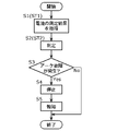
- FIG. 4 is a flowchart showing an operation example of the arc detection system according to the first embodiment.
- FIG. 5 is a schematic diagram showing an overall configuration including the arc detection system according to the second embodiment.
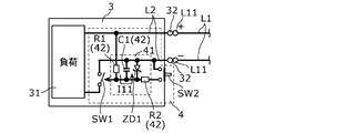
- FIG. 1 is a schematic diagram showing an overall configuration including an arc detection system 100 according to the first embodiment.
- the arc detection system 100 is a system for determining whether or not an arc failure has occurred in the power supply path L1 to which power is mainly supplied from the DC power supply 2. That is, the power supply path L1 may be damaged or broken due to, for example, an external factor or aged deterioration, and an arc (arc discharge) is generated due to such damage, resulting in an arc failure. there's a possibility that. Therefore, the arc detection system 100 is mainly used for detecting an arc failure that may occur in the feeding path L1.
- the arc detection system 100 is used for a so-called DC (Direct Current) distribution network 200.
- the DC distribution network 200 is configured to include one or more power supply paths L1. In FIG. 1, only one power supply path L1 is shown. DC power is supplied to the DC distribution network 200 from the DC power source 2.
- Each power supply path L1 is composed of a pair of electric circuits, that is, a positive power supply path connected to the positive electrode on the output side of the DC power supply 2 and a negative power supply path connected to the negative electrode on the output side of the DC power supply 2. There is.
- DC power is supplied from the DC power supply 2 to this power supply path L1.
- the DC distribution network 200 has a plurality of power supply paths L1, one end of each of the plurality of power supply paths L1 is connected to one or more branch points. Therefore, when DC power is supplied from the DC power source 2 to any of the power supply paths L1, DC power is also supplied to the other power supply paths L1 via one or more branch points.
- the DC power supply 2 is a power converter including an AC / DC converter 21.
- the DC power supply 2 converts the AC power output from the power system 300 into DC power, and outputs the converted DC power to the power supply path L1 to which the DC power supply 2 is connected.
- the DC distribution network 200 has a plurality of power supply paths L1
- the DC power output to the power supply path L1 is also output to the other power supply paths L1.
- the DC power supply 2 may be a mode that outputs DC power, and may be a distributed power source such as a solar cell or a power source such as a storage battery, or these power sources and a power converter (for example, DC / It may be a combination with a power converter provided with a DC converter circuit).
- Each power supply path L1 is composed of, for example, a duct rail, and one or more devices 3 can be attached to it. That is, in each power supply path L1, one or more devices 3 can be arranged at free positions. Of course, each power supply path L1 may have a mode in which a place where one or more devices 3 can be attached is predetermined. In the first embodiment, each power supply path L1 is arranged on the ceiling of the facility, but may be arranged on the floor, wall, furniture, or the like of the facility.
- the device 3 has a load 31 and a pair of connection terminals 32.
- the device 3 can be attached to or removed from the power supply path L1 via the pair of connection terminals 32.
- the device 3 is rotated clockwise when viewed from the insertion direction of the device 3 with the pair of connection terminals 32 of the device 3 inserted into the duct rail (power supply path L1).
- a predetermined angle for example, 90 degrees.
- the pair of connection terminals 32 are fixed in contact with the pair of connection conductors L11 provided in the power supply path L1, and the device 3 is electrically and mechanically connected to the power supply path L1.
- the device 3 When the device 3 is removed from the power supply path L1, the device 3 is rotated by a predetermined angle in the opposite direction to the above when viewed from the insertion direction of the device 3. As a result, the contact state between the pair of connection terminals 32 and the pair of connection conductors L11 is released, so that the device 3 can be subsequently removed from the power supply path L1.
- the load 31 is driven by receiving DC power supplied from the DC power supply 2 via the power supply path L1 in a state where the device 3 is attached to the power supply path L1.
- the device 3 is a lighting fixture, but may be, for example, a speaker, a camera, a sensor, a USB PD (Power Delivery), or the like. That is, the device 3 may be a device other than the lighting fixture as long as the load 31 is driven by receiving electric power. Further, in the first embodiment, all the devices 3 connected to each power supply path L1 are lighting fixtures and have one type, but even if there are a plurality of types of devices 3 connected to each power supply path L1. good. For example, a lighting fixture, a speaker, a camera, a sensor, and a USB PD may be connected to each power supply path L1. All of these devices 3 may be connected to one power supply path L1, or may be divided and connected to a plurality of power supply paths L1.
- the arc detection system 100 includes an acquisition unit 11, a determination unit 12, a notification unit 13, a stop unit 14, a suppression circuit 4, and functional components for determining whether or not an arc failure has occurred. It is equipped with.
- the acquisition unit 11, the determination unit 12, the notification unit 13, and the stop unit 14 are provided in the DC power supply 2, and the suppression circuit 4 is provided in each device 3.
- the arc detection system 100 is, for example, a microcomputer or a device including a microcomputer.
- the microcomputer is a semiconductor integrated circuit having a ROM and RAM in which a program is stored, a processor (CPU: Central Processing Unit) for executing the program, a timer, an A / D converter, a D / A converter, and the like.
- the acquisition unit 11, the determination unit 12, the notification unit 13, and the stop unit 14 are all realized by the processor executing the above program.
- the acquisition unit 11 acquires the measurement result of the current I1 flowing in the power supply path L1 to which the power is supplied from the DC power supply 2.
- the acquisition unit 11 acquires the measurement result of the current I1 measured by sampling at a predetermined cycle (sampling cycle) with the ammeter 22. That is, the acquisition unit 11 acquires the measurement result of the current I1 from the ammeter 22 at a predetermined cycle.
- the ammeter 22 is provided between the DC power supply 2 and the power supply path L1 and measures the current flowing in the negative power supply path of the power supply path L1 (that is, the current I1 flowing in the power supply path L1).
- the ammeter 22 may be built in the DC power supply 2.
- the determination unit 12 determines whether or not an arc failure has occurred based on the component of a specific frequency band in the measurement result of the current I1 acquired by the acquisition unit 11. Specifically, the determination unit 12 frequency-analyzes the measurement result of the current I1 acquired by the acquisition unit 11. The frequency analysis is to calculate the frequency spectrum of the measurement result of the current I1 by, for example, Fourier transforming (here, FFT (FastFourier Transform)) the time waveform of the measurement result of the current I1. Then, the determination unit 12 determines whether or not an arc failure has occurred by referring to the calculated frequency spectrum.
- the specific frequency band is, for example, a band including the frequency of noise generated when an arc failure occurs.
- the specific frequency band is, for example, a tens of kHz band, which is a relatively high frequency band. The frequency of noise generated in the above cases can be obtained experimentally.
- the determination unit 12 compares the specific time at which the component of the specific frequency band is equal to or greater than the threshold value with the preset threshold time (for example, 1 second), and when the specific time is longer than the threshold time, It is determined that an arc failure has occurred.
- the threshold time is preset based on the arc generation time that can occur when the device 3 is attached to or detached from the power supply path L1. That is, the determination unit 12 has encountered an arc failure when the specific time in which the component of the specific frequency band is equal to or greater than the threshold value is longer than the arc generation time that can occur when the device 3 is attached to or detached from the power supply path L1. Is determined.
- the process leading to the determination of the occurrence of the arc failure will be described.
- the arcs that can be generated in the DC distribution network 200 include an arc caused by a disconnection or a half disconnection of the power supply path L1 and an arc that can be instantaneously generated when the device 3 is attached to and detached from the power supply path L1. That is, when the device 3 is attached to the power supply path L1, if the device 3 is not smoothly attached, the load 31 of the device 3 is connected to the power supply path L1 and is disconnected from the power supply path L1. Is repeated in a short period of time, so-called chattering may occur. Then, during the chattering generation period, an arc may occur when the load 31 is momentarily disconnected from the feeding path L1 while the current is flowing.
- chattering may occur in the same manner as described above. Then, during the chattering generation period, an arc may occur when the load 31 is momentarily disconnected from the feeding path L1 while the current is flowing.
- the generation of arcs due to such chattering can occur not only in the DC distribution network 200 but also in the AC distribution network.
- the current flowing in the feeding path is an alternating current, there is a moment when the current becomes zero, so that the duration of the arc caused by chattering tends to be short. Specifically, the duration of the arc is less than half the period of the alternating current.
- the current flowing through the feeding path L1 is a direct current
- the current does not become zero and the duration of the arc due to chattering tends to be long.
- the device 3 is attached to the feeding path L1 while the distance between the electrode of the device 3 and the electrode of the feeding path L1 is halfway, the arc is less likely to disappear.
- the arc caused by the disconnection or half disconnection of the power supply path L1 tends to cause an arc failure, but the arc caused by chattering basically disappears in a short period of time, so that it is unlikely to cause an arc failure. Therefore, in the arc detection system 100, it is desired to determine that the occurrence of an arc mainly due to a disconnection or a half disconnection of the power supply path L1 is the occurrence of an arc failure without detecting a short-time arc due to chattering. ..
- the suppression circuit 4 is provided in each device 3 in order to satisfy the above-mentioned request.
- the suppression circuit 4 is configured so that when the device 3 is attached to the power supply path L1, the load 31 is connected to the power supply path L1 with a delay time.
- the load 31 will be connected to the power supply path L1 after the device 3 will be securely attached to the power supply path L1, and the load 31 will be connected to the power supply path L1 with the above-mentioned current flowing.
- the situation of momentary disconnection is unlikely to occur, and as a result, the arc caused by chattering is less likely to occur.
- the suppression circuit 4 is disconnected from the power supply path L1 of the device 3 before the device 3 is removed from the power supply path L1. It is configured as follows. As a result, the device 3 is removed from the power supply path L1 after the device 3 is disconnected from the power supply path L1, and the load 31 is instantaneously disconnected from the power supply path L1 with the above-mentioned current flowing. Situations are less likely to occur, and as a result, arcs due to chattering are less likely to occur.
- the determination unit 12 is not an arc caused by chattering, but a disconnection or disconnection in the feeding path L1. It is determined that an arc is generated due to a half disconnection, that is, an arc failure has occurred. That is, in the first embodiment, the specific time is longer than the delay time.
- the suppression circuit 4 does not exist, it is considered that an arc due to chattering may occur in a period corresponding to the delay time. Therefore, the fact that the specific time is longer than the delay time corresponds to the specific time being longer than the arc generation time that can occur when the device 3 is attached to or detached from the power supply path L1.
- an arc due to chattering may occur when the device 3 is attached to or detached from the power supply path L1.
- the determination unit 12 does not determine that an arc failure has occurred even if an arc caused by chattering occurs.
- an arc failure may occur due to an arc caused by chattering.
- the determination unit 12 can determine that the arc failure has occurred even in such a case.
- the notification unit 13 notifies the surroundings that an arc failure has occurred, for example, by turning on a lamp or sounding a buzzer. Further, the notification unit 13 notifies that an arc failure has occurred by transmitting information indicating that an arc failure has occurred to an information terminal owned by the owner or administrator of the arc detection system 100. You may.
- the information terminal may include a personal computer or the like as well as a mobile terminal such as a smartphone or a tablet.
- the stop unit 14 stops the current flowing in the power supply path L1 when the determination unit 12 determines that an arc failure has occurred. As a result, if an arc discharge is generated due to an arc failure, the arc discharge disappears.
- the stop unit 14 stops the current flowing in the power supply path L1 by controlling the switch connected to the power supply path L1.
- the switch is, for example, a mechanical switch or a semiconductor switch.
- the mechanical switch is, for example, a switch such as a relay or a breaker
- the semiconductor switch is a switch such as a transistor or a diode.
- the switch connected to the power supply path L1 may be a switch directly connected to the power supply path L1 or a switch indirectly connected to the power supply path L1.
- the switch is a switch for realizing the AC / DC conversion function in the AC / DC converter 21. Even if the switch is not directly connected to the power supply path L1, it is indirectly connected to the power supply path L1, so that the switch is connected to the power supply path L1.
- the stop unit 14 controls the switch to stop the switching operation of the switch, thereby stopping the current flowing in the power supply path L1.
- the switch may be configured to switch the DC power supply 2 on and off.
- the stop unit 14 controls the switch to turn off the DC power supply 2 to stop the current flowing in the power supply path L1.
- the switch may be provided on the power supply path L1, and the switch may be configured to switch the opening and closing of the power supply path L1.
- the stop unit 14 may stop the current flowing in the power supply path L1 by controlling the switch to open the power supply path L1.
- the suppression circuit 4 is a circuit for suppressing an arc that may occur when the device 3 is attached to or detached from the power supply path L1.
- the suppression circuit 4 has a first switch SW1, a second switch SW2, and a drive circuit 41.
- the suppression circuit 4 is provided between the load 31 of the device 3 and the pair of connection terminals 32 in each device 3.
- the first switch SW1 opens and closes the electric circuit L2 between the load 31 of the device 3 and the power supply path L1.
- the electric circuit L2 has an electric circuit connecting the connection terminal 32 on the positive electrode side of the pair of connection terminals 32 and the positive electrode of the load 31, and the connection terminal 32 on the negative electrode side of the pair of connection terminals 32 and the negative electrode of the load 31. It consists of an electric circuit to connect.
- the electric circuit L2 is closed to electrically connect the pair of connection terminals 32 and the load 31. In this state, when the device 3 is attached to the power supply path L1, electric power is supplied from the power supply path L1 to the load 31 (that is, a current flows).
- the electric path L2 is opened to electrically disconnect the pair of connection terminals 32 and the load 31. In this state, even if the device 3 is attached to the power supply path L1, power is not supplied from the power supply path L1 to the load 31 (that is, no current flows).
- the first switch SW1 is an n-channel enhancement type MOSFET (Metal-Oxide-Semiconductor Field-Effect Transistor). That is, the first switch SW1 is a field effect transistor.
- FIG. 1 the symbol of the diode between the drain and the source represents the parasitic diode of the first switch SW1. The same applies to FIG. 5, which will be described later.
- the drain of the first switch SW1 is connected to the negative electrode of the load 31, and the source of the first switch SW1 is connected to the negative connection terminal 32 of the pair of connection terminals 32.
- the gate of the first switch SW1 is connected to the drive circuit 41.
- the drive circuit 41 drives the first switch SW1 so as to close the electric circuit L2 after the lapse of the delay time after the device 3 is connected to the electric circuit L2.
- the drive circuit 41 is connected to the gate of the first switch SW1 and includes a CR filter 42 that applies the charging voltage of the capacitor C1 to the gate of the first switch SW1.
- the delay time is determined by the time constant of the CR filter 42.
- the drive circuit 41 has a first resistance element R1, a second resistance element R2, a capacitor C1, and a Zener diode ZD1.
- the CR filter 42 is composed of the first resistance element R1, the second resistance element R2, and the capacitor C1.
- One end of the first resistance element R1 is connected to the positive connection terminal 32 of the pair of connection terminals 32 and the positive electrode of the load 31, and the other end of the first resistance element R1 is the gate of the first switch SW1. It is connected to the.
- One end of the second resistance element R2 is connected to the gate of the first switch SW1, and the other end of the second resistance element R2 is connected to the negative side of the pair of connection terminals 32 via the second switch SW2. It is connected to the terminal 32.
- One end of the capacitor C1 is connected to the gate of the first switch SW1, and the other end of the capacitor C1 is connected to the source of the first switch SW1.
- the Zener diode ZD1 is connected between the gate and the source of the first switch SW1 and suppresses an excessive voltage from being applied between the gate and the source of the first switch SW1.
- the Zener diode ZD1 is replaced with a resistor whose voltage division ratio with the first resistance element R1 is set so that the gate-source voltage of the first switch SW1 becomes a voltage sufficient to switch to the ON state. May be good. Further, a resistor may be further connected in parallel with the Zener diode ZD1. The same applies to the second embodiment described later.
- the delay time is set so that power is not supplied to the device 3 during the chattering generation period that may occur when the device 3 is attached to and detached from the power supply path L1.
- the second switch SW2 is configured to switch between the gate of the first switch SW1 and the electric circuit L2 from one of the short-circuited state and the open state to the other.
- the second switch SW2 is a normally-off type push button switch and is exposed to the outside of the device 3.
- the second switch SW2 switches to the on state (that is, a short-circuit state) only while the user is performing the push operation, and maintains the off state (that is, the open state) while the user is not performing the push operation.
- One end of the second switch SW2 is connected to the gate of the first switch SW1 via the second resistance element R2, and the other end of the second switch SW2 is the negative connection terminal of the pair of connection terminals 32. It is connected to 32.
- FIGS. 2A to 3B are schematic views showing the operation of the suppression circuit 4 at the time of attachment / detachment to / from the power supply path L1 of the device 3.
- the expression of the first switch SW1 is different from that of FIG. 1 in order to make it easier to visually understand the on / off of the first switch SW1.
- the operation of the suppression circuit 4 when the device 3 is attached to the power supply path L1 will be described.
- the user attaches the device 3 to the power supply path L1 while operating the second switch SW2.
- the first switch SW1 is turned off. It is in a state, and the electric circuit L2 is open.
- the device 3 is electrically connected to the power supply path L1, but since the second switch SW2 is in the ON state, the charging current I11 does not flow through the capacitor C1 and the first switch SW1 does not turn on. ..
- the user inserts the device 3 into the power supply path L1 while operating the second switch SW2, and rotates the device 3 by a predetermined angle to electrically and mechanically connect the device 3 to the power supply path L1. This completes the attachment of the device 3 to the power supply path L1. After that, the user releases the second switch SW2 to turn off the second switch SW2. That is, as long as the user is operating the second switch SW2, in other words, the first switch SW1 is basically not turned on until the user completes the attachment of the device 3 to the power supply path L1.
- the charging current I11 flows through the capacitor C1 via the first resistance element R1 in the CR filter 42 of the drive circuit 41, so that charging of the capacitor C1 is started.
- the capacitor C1 is charged according to a time constant based on the resistance value of the first resistance element R1 and the capacitance value of the capacitor C1.
- the suppression circuit 4 turns on the first switch SW1 after the lapse of the delay time from the time when the device 3 is connected to the electric circuit L2 (here, the time when the second switch SW2 is turned off). Power is supplied from the power supply path L1 to the load 31 after the delay time has elapsed from the time point. Therefore, even if chattering occurs when the device 3 is attached to the power supply path L1, power is not supplied from the power supply path L1 to the load 31 during the chattering generation period, so that it is possible to suppress the generation of an arc due to chattering. can.
- the user may forget to operate the second switch SW2.
- the charging current I11 starts to flow in the capacitor C1 from the time of contact.
- the suppression circuit 4 turns on the first switch SW1 after the delay time has elapsed from the time when the device 3 is connected to the electric circuit L2 (here, the contact time)
- the delay time elapses from the above time.
- power is supplied from the power supply path L1 to the load 31. Therefore, even if chattering occurs in such a case, it becomes difficult to supply electric power from the power supply path L1 to the load 31 during the chattering generation period, so that the effect of suppressing the generation of an arc due to chattering can be expected.
- the operation of the suppression circuit 4 when the device 3 is removed from the power supply path L1 will be described.
- the user removes the device 3 from the power supply path L1 while operating the second switch SW2.
- the second switch SW2 is turned on before the device 3 is removed from the power supply path L1.
- the discharge current I12 flows from the capacitor C1 to the feeding path L1 via the second resistance element R2, so that the discharge of the capacitor C1 is started.
- the capacitor C1 is discharged according to a time constant based on the resistance value of the second resistance element R2 and the capacitance value of the capacitor C1.
- the suppression circuit 4 turns off the first switch SW1 after the lapse of the delay time from the time when the second switch SW2 is turned on, so that the power supply path of the device 3 is before the device 3 is removed from the power supply path L1.
- the electrical connection to L1 is disconnected. Therefore, even if chattering occurs when the device 3 is removed from the power supply path L1, power is not supplied from the power supply path L1 to the load 31 during the chattering generation period, so that it is possible to suppress the generation of an arc due to chattering. can.
- the device 3 may be removed from the power supply path L1 before the delay time elapses.
- an arc may be generated when the device 3 is removed from the feeding path L1, but the arc generation time can be shortened as compared with the case where the suppression circuit 4 does not exist, resulting in chattering. It can be said that the generation of arc is suppressed.
- the resistance value of the second resistance element R2 is preferably smaller than the resistance value of the first resistance element R1. If the resistance value of the second resistance element R2 is small, the delay time until the first switch is turned off becomes short. If this delay time is short, it is less likely that the device 3 is attached to and detached from the power supply path L1 at a time earlier than the delay time, and an arc due to chattering is less likely to occur. However, the shorter the delay time is, the more preferable it is, and if it is made extremely short, conversely, an arc due to the first switch SW1 being turned off in an instant may occur. Therefore, for example, this delay time is preferably about several tens of milliseconds.
- the load 31 may be connected to the feeding path L1 after the device 3 is surely attached to the feeding path L1, so that the first switch SW1 is turned on.
- the delay time may be long. However, if this delay time is made extremely long, the time from when the device 3 is attached to the power supply path L1 until the load 31 is actually driven becomes long, and the user may feel a sense of discomfort. Therefore, for example, this delay time is preferably about several hundred milliseconds.
- FIG. 4 is a flowchart showing an operation example of the arc detection system 100 according to the first embodiment.
- the acquisition unit 11 acquires the measurement result of the current I1 from the ammeter 22 at a predetermined cycle (S1).
- the process S1 corresponds to the acquisition step ST1 of the arc detection method.
- the determination unit 12 determines whether or not an arc failure has occurred based on the component of a specific frequency band in the measurement result of the current I1 acquired by the acquisition unit 11 (S2).
- the determination unit 12 determines by frequency analysis of the measurement result of the current I1 acquired by the acquisition unit 11.
- the determination unit 12 compares the component of the specific frequency band with the threshold value, and the specific time when the component of the specific frequency band is equal to or higher than the threshold value and the state continues is the threshold time. If it is longer than, it is determined that an arc failure has occurred (S3: Yes). On the other hand, the determination unit 12 determines that no arc failure has occurred when the specific time has not reached the threshold time or when the component of the specific frequency band is below the threshold value (S3: No).
- the processes S2 and S3 correspond to the determination step ST2 of the arc detection method.
- the stop unit 14 stops the current flowing through the power supply path L1 to supply power from the DC power supply 2 to the power supply path L1. Is stopped (S4). Then, the notification unit 13 notifies the occurrence of an arc failure (S5). On the other hand, when the determination unit 12 determines that no arc failure has occurred (S3: No), the processing of the arc detection system 100 ends. Hereinafter, the above series of processes S1 to S5 are repeated.
- the arc detection system of the comparative example is implemented in that when the component of a specific frequency band in the measurement result of the current I1 acquired by the acquisition unit 11 exceeds the threshold value, it is immediately determined that an arc failure has occurred. It is different from the arc detection system 100 according to the first embodiment.
- the conditions required for the arc detection system will be explained. If an arc is generated due to a break or half break in the feeder line L1, if this state is left unattended, the broken or half broken part will generate excessive heat, and in some cases, it may ignite and lead to a fire. be. Therefore, it is important for the arc detection system to detect the occurrence of an arc (that is, the occurrence of an arc failure) as soon as possible, and to stop the power supply to the power supply path L1 before a situation such as a fire occurs. For example, the UL (Underwriters Laboratories) standard requires that the occurrence of an arc failure be detected within 2 seconds after the occurrence of an arc.
- an event such as notifying the user that an arc failure has occurred may occur, which is troublesome for the user.
- the power supply from the DC power supply 2 to the power supply path L1 is automatically stopped when it is determined that an arc failure has occurred.
- an event may occur in which the power supply to the power supply path L1 is stopped each time the device 3 is attached to or detached from the power supply path L1, which is also troublesome for the user.
- the arc detection system 100 it is determined that an arc failure has occurred when an arc due to a disconnection or a half disconnection of the feeding path L1 has occurred, and when an arc due to chattering has occurred. Basically does not determine that an arc failure has occurred. That is, in the arc detection system 100 according to the first embodiment, it is unlikely that the arc failure is determined to have occurred due to the generation of an arc that is unlikely to cause the arc failure. In other words, the arc detection system 100 according to the first embodiment does not detect an event that does not lead to an arc failure even if it occurs temporarily, such as an arc that may occur when the device 3 is attached to or detached from the power supply path L1.
- FIG. 5 is a schematic diagram showing an overall configuration including the arc detection system 100 according to the second embodiment.
- the DC power supply 2 is not shown. Therefore, in FIG. 5, the acquisition unit 11, the determination unit 12, the notification unit 13, and the stop unit 14, which are the components of the arc detection system 100, are not shown.
- the configuration of the suppression circuit 4A is different from the configuration of the suppression circuit 4 in the arc detection system 100 according to the first embodiment.
- the differences from the first embodiment will be mainly described, and the common points with the first embodiment will be omitted as appropriate.
- the suppression circuit 4A has a first switch SW1, a second switch SW2, and a drive circuit 41, similarly to the suppression circuit 4 of the first embodiment.
- the arrangement of the components of the first switch SW1, the second switch SW2, and the drive circuit 41 is different from that of the suppression circuit 4 of the first embodiment.
- the drive circuit 41 of the second embodiment further has a power supply circuit 43, unlike the suppression circuit 4 of the first embodiment.
- the first switch SW1 is an n-channel enhancement type MOSFET as in the first embodiment.
- the drain of the first switch SW1 is connected to the positive connection terminal 32 of the pair of connection terminals 32, and the source of the first switch SW1 is connected to the positive electrode of the load 31.
- the gate of the first switch SW1 is connected to the drive circuit 41.
- the second switch SW2 is a normally-off type push button switch as in the first embodiment. One end of the second switch SW2 is connected to the gate of the first switch SW1 via the second resistance element R2, and the other end of the second switch SW2 is the positive connection terminal of the pair of connection terminals 32. It is connected to 32.
- the drive circuit 41 includes a first resistance element R1, a second resistance element R2, a capacitor C1, a Zener diode ZD1, and a power supply circuit 43.
- the CR filter 42 is composed of the first resistance element R1, the second resistance element R2, and the capacitor C1.
- One end of the first resistance element R1 is connected to the gate of the first switch SW1, and the other end of the first resistance element R1 is connected to the high voltage side output terminal 432 of the pair of output terminals 432 of the power supply circuit 43. It is connected.
- One end of the second resistance element R2 is connected to the gate of the first switch SW1, and the other end of the second resistance element R2 is connected to the positive side of the pair of connection terminals 32 via the second switch SW2. It is connected to the terminal 32.
- One end of the capacitor C1 is connected to the gate of the first switch SW1, and the other end of the capacitor C1 is connected to the source of the first switch SW1.
- the Zener diode ZD1 is connected between the gate and the source of the first switch SW1 and suppresses an excessive voltage from being applied between the gate and the source of the first switch SW1.
- the power supply circuit 43 has a pair of input terminals 431 and a pair of output terminals 432, and the pair of input terminals 431 and the pair of output terminals 432 are electrically isolated from each other. Further, the power supply circuit 43 generates a drive voltage for driving the gate of the first switch SW1 based on the voltage applied to the pair of input terminals 431, and outputs the generated drive voltage from the pair of output terminals 432. do.
- the pair of input terminals 431 are each connected to the pair of connection terminals 32.
- the high-voltage side output terminal 432 of the pair of output terminals 432 is connected to the gate of the first switch SW1 via the first resistance element R1, and the low-voltage side output terminal 432 is connected to the positive electrode of the load 31. Has been done.
- the time constant and the delay time are determined based on the resistance value of the first resistance element R1 and the capacitance value of the capacitor C1.
- the time constant and the delay time are determined based on the resistance value of the second resistance element R2 and the capacitance value of the capacitor C1.
- the operation of the suppression circuit 4A will be described.
- the operation of the suppression circuit 4A when the device 3 is attached to the power supply path L1 will be described.
- the user attaches the device 3 to the power supply path L1 while operating the second switch SW2.
- the first switch SW1 is in the off state and the electric circuit L2 is in the off state. It is open.
- the device 3 is electrically connected to the power supply path L1, but since the second switch SW2 is in the ON state, the charging current does not flow through the capacitor C1 and the first switch SW1 does not turn on.
- the user inserts the device 3 into the power supply path L1 while operating the second switch SW2, and rotates the device 3 by a predetermined angle to electrically and mechanically connect the device 3 to the power supply path L1. This completes the attachment of the device 3 to the power supply path L1. After that, the user releases the second switch SW2 to turn off the second switch SW2. That is, as long as the user is operating the second switch SW2, in other words, the first switch SW1 is basically not turned on until the user completes the attachment of the device 3 to the power supply path L1.
- the capacitor C1 is sufficiently charged and the charging voltage of the capacitor C1 (that is, the gate-source voltage of the first switch SW1) reaches a predetermined voltage, the first switch SW1 is turned on and the electric circuit L2 is turned on. Closed. As a result, electric power is supplied from the power supply path L1 to the load 31.
- the operation of the suppression circuit 4A when the device 3 is removed from the power supply path L1 will be described.
- the user removes the device 3 from the power supply path L1 while operating the second switch SW2.
- the second switch SW2 is turned on before the device 3 is removed from the power supply path L1.
- the discharge current flows from the capacitor C1 to the feeding path L1 via the second resistance element R2, so that the discharge of the capacitor C1 is started.
- the capacitor C1 is discharged according to a time constant based on the resistance value of the second resistance element R2 and the capacitance value of the capacitor C1.
- the charging voltage of the capacitor C1 that is, the gate-source voltage of the first switch SW1
- the first switch SW1 is turned off and the electric circuit L2 is turned off. Be released.
- electric power is not supplied from the power supply path L1 to the load 31.
- the pair of connection terminals 32 of the device 3 and the pair of connection conductors L11 of the power supply path L1 are separated from each other, so that the device 3 is electrically connected to the power supply path L1. The connection is disconnected.
- the suppression circuit 4A operates in the same manner as the suppression circuit 4 of the first embodiment. Further, the arc detection system 100 according to the second embodiment has the same configuration as the arc detection system 100 according to the first embodiment, except for the suppression circuit 4A. Therefore, the arc detection system 100 according to the second embodiment can have the same effect as the arc detection system 100 according to the first embodiment.
- the ammeter 22 is a device different from the arc detection system 100, but may be built in the arc detection system 100.
- the arc detection system 100 is provided in the DC power supply 2, but the present invention is not limited to this.
- the arc detection system 100 may be connected to the power supply path L1 as a device separate from the DC power supply 2.
- the arc detection system 100 if the arc detection system 100 is configured to be able to communicate with the DC power supply 2 by wire communication or wireless communication, the arc detection system 100 gives an instruction to the DC power supply 2 according to the determination result of the determination unit 12. Is possible.
- the determination unit 12 extracts the component of a specific frequency band by performing frequency analysis on the measurement result of the current I1 acquired by the acquisition unit 11.
- the determination unit 12 extracts the frequency component of a specific frequency band by passing the measurement result of the current I1 acquired by the acquisition unit 11 through a filter (for example, a bandpass filter) instead of executing the frequency analysis. You may.
- the second switch SW2 is configured to be turned on / off by being operated by the user's hand, but the present invention is not limited to this.
- the second switch SW2 may be configured to automatically switch on / off according to the attachment / detachment of the device 3 to / from the power supply path L1.
- the second switch SW2 may be configured to temporarily switch to a short-circuited state at least when the device 3 is removed from the power supply path L1.
- the second switch SW2 is a normally-on type push button switch, and is configured to switch to an off state (open state) when a predetermined force is applied. That is, the second switch SW2 maintains an on state (short-circuited state) when the device 3 is not attached to the power supply path L1, and a predetermined force is applied when the device 3 is attached to the power supply path L1. Switch to the off state.
- the operation of the second switch SW2 in the above specific example will be described.
- the device 3 is first inserted into the power supply path L1.
- the second switch SW2 is still in the on state.
- the device 3 is connected to the power supply path L1 by rotating the device 3 by a predetermined angle.
- a predetermined force is applied to the second switch SW2 from the device 3 and the power supply path L1 as the device 3 rotates.
- the second switch SW2 is switched to the off state.
- the second switch SW2 maintains the off state.
- the second switch SW2 automatically switches on / off according to the attachment / detachment of the device 3 to / from the power supply path L1 without the user having to directly operate it. Then, the second switch SW2 switches to the ON state before the device 3 is removed from the power supply path L1 (that is, at least temporarily switches to the short-circuit state when the device 3 is removed from the power supply path L1). In this configuration, similar to the case where the user operates the second switch SW2 when removing the device 3 from the power supply path L1, the electrical connection of the device 3 to the power supply path L1 before the device 3 is removed from the power supply path L1. Is to be released.
- the suppression circuits 4 and 4A do not have to have the second switch SW2.
- the arc detection system 100 may not include the notification unit 13 and the stop unit 14. That is, the arc detection system 100 only needs to have a function of detecting the occurrence of an arc failure, and the notification unit 13 and the stop unit 14 may be realized by another system.
- the suppression circuits 4 and 4A are provided in each device 3, but the present invention is not limited to this.
- the suppression circuits 4 and 4A may be provided only in a part of the devices 3 among the plurality of devices 3. Further, for example, none of the devices 3 may be provided with the suppression circuits 4 and 4A. That is, the arc detection system 100 does not have to include the suppression circuits 4 and 4A. Further, for example, the suppression circuits 4 and 4A may be provided separately from the device 3 in a connector for connecting the device 3 and the power supply path L1 to each other.
- the present invention can be realized not only as an arc detection system 100 but also as an arc detection method including steps (processes) performed by each component constituting the arc detection system 100.
- the arc detection method includes acquisition step ST1 and determination step ST2.
- the acquisition step ST1 the measurement result of the current I1 flowing in the power supply path L1 to which the power is supplied from the DC power supply 2 is acquired.
- the determination step ST2 it is determined whether or not an arc failure has occurred based on the component of a specific frequency band in the measurement result of the current I1 acquired in the acquisition step ST1.
- the determination step ST2 it is determined that an arc failure has occurred when the specific time in which the component of the specific frequency band is equal to or higher than the threshold value is longer than the arc generation time that can occur when the device 3 is attached to or detached from the power supply path L1. do.
- those steps may be performed by a computer (computer system) having one or more processors.
- the present invention can be realized as a program for causing a computer to execute the steps included in those methods.
- the present invention can be realized as a non-temporary computer-readable recording medium such as a CD-ROM in which the program is recorded.
- the program causes one or more processors to execute the above arc detection method.
- the arc detection system 100 is realized by software by a microcomputer, it may be realized by software in a general-purpose computer such as a personal computer. Further, at least a part of the arc detection system 100 may be realized by hardware by a dedicated electronic circuit composed of an A / D converter, a logic circuit, a gate array, a D / A converter and the like.
- the suppression circuits 4 and 4A in the first and second embodiments can be distributed on the market independently of the arc detection system 100. That is, the suppression circuits 4 and 4A include a first switch SW1 and a drive circuit 41.
- the first switch SW1 opens and closes the electric line L2 between the power supply path L1 to which electric power is supplied from the DC power source 2 and the load 31 of the device 3 that can be attached to and detached from the power supply path L1.
- the drive circuit 41 drives the first switch SW1 so as to close the electric circuit L2 after a delay time elapses after the device 3 is connected to the electric circuit L2.
- the suppression circuits 4 and 4A may be configured as follows, for example. That is, the first switch SW1 is a field effect transistor.
- the drive circuit 41 is further provided with a CR filter 42 which is connected to the gate of the first switch SW1 and applies the charging voltage of the capacitor C1 to the gate of the first switch SW1.
- the delay time is determined by the time constant of the CR filter 42.
- the suppression circuits 4 and 4A may be configured as follows, for example. That is, the suppression circuits 4 and 4A further include a second switch SW2 that switches between the gate of the first switch SW1 and the electric circuit L2 from one of the short-circuited state and the open state to the other.
- suppression circuits 4 and 4A may be configured as follows, for example. That is, the second switch SW2 is configured to temporarily switch to the short-circuited state when at least the device 3 is removed from the power supply path L1.
- the suppression circuits 4 and 4A may be configured as follows, for example. That is, the delay time is set so that power is not supplied to the device 3 during the chattering generation period that may occur when the device 3 is attached to or detached from the power supply path L1.
- the first switch SW1 is not limited to the field effect transistor, and may be, for example, a relay or the like.
- the arc detection system 100 includes an acquisition unit 11 and a determination unit 12.
- the acquisition unit 11 acquires the measurement result of the current I1 flowing in the power supply path L1 to which the power is supplied from the DC power supply 2.
- the determination unit 12 determines whether or not an arc failure has occurred based on the component of a specific frequency band in the measurement result of the current I1 acquired by the acquisition unit 11.
- the determination unit 12 determines that an arc failure has occurred when the specific time in which the component of the specific frequency band is equal to or higher than the threshold value is longer than the arc generation time that can occur when the device 3 is attached to or detached from the power supply path L1. do.
- an arc detection system 100 it is not necessary to detect an event that does not lead to an arc failure even if it occurs temporarily, such as an arc that may occur when the device 3 is attached to or detached from the power supply path L1. There is an advantage that it becomes easy to prevent false detection of the occurrence of an arc failure.
- the arc detection system 100 further includes suppression circuits 4 and 4A that suppress an arc that may occur when the device 3 is attached to and detached from the power supply path L1.
- the suppression circuits 4 and 4A include a first switch SW1 and a drive circuit 41.
- the first switch SW1 opens and closes the electric circuit L2 between the load 31 of the device 3 and the power supply path L1.
- the drive circuit 41 drives the first switch SW1 so as to close the electric circuit L2 after a delay time elapses after the device 3 is connected to the electric circuit L2.
- the load 31 of the device 3 will be connected to the power supply path L1 after the device 3 will be attached to the power supply path L1, so that the current flows.
- the situation in which the load 31 is momentarily disconnected from the power supply path L1 is less likely to occur.
- there is an advantage that an arc due to chattering that may occur when the device 3 is attached to and detached from the power supply path L1 is less likely to occur.
- the first switch SW1 is a field effect transistor.
- the drive circuit 41 is further provided with a CR filter 42 which is connected to the gate of the first switch SW1 and applies the charging voltage of the capacitor C1 to the gate of the first switch SW1.
- the delay time is determined by the time constant of the CR filter 42.
- the load 31 of the device 3 will be connected to the power supply path L1 after the device 3 will be attached to the power supply path L1, so that the current flows.
- the situation in which the load 31 is momentarily disconnected from the power supply path L1 is less likely to occur.
- there is an advantage that an arc due to chattering that may occur when the device 3 is attached to and detached from the power supply path L1 is less likely to occur.
- the suppression circuits 4 and 4A further include a second switch SW2 that switches between the gate of the first switch SW1 and the electric circuit L2 from one of the short-circuited state and the open state to the other.
- the second switch SW2 is configured to temporarily switch to a short-circuit state when at least the device 3 is removed from the power supply path L1.
- the delay time is set so that power is not supplied to the device 3 during the chattering generation period that may occur when the device 3 is attached to or detached from the power supply path L1.
- the specific time is longer than the delay time.
- the arc detection method includes acquisition step ST1 and determination step ST2.
- acquisition step ST1 the measurement result of the current I1 flowing in the power supply path L1 to which the power is supplied from the DC power supply 2 is acquired.
- determination step ST2 it is determined whether or not an arc failure has occurred based on the component of a specific frequency band in the measurement result of the current I1 acquired in the acquisition step ST1.
- determination step ST2 it is determined that an arc failure has occurred when the specific time in which the component of the specific frequency band is equal to or higher than the threshold value is longer than the arc generation time that can occur when the device 3 is attached to or detached from the power supply path L1. do.
- the program causes one or more processors to execute the above arc detection method.
Abstract
This arc detection system (100) comprises an acquisition unit (11) and a determination unit (12). The acquisition unit (11) acquires the measurement result of current (I1) flowing through a feeding path (L1) to which power is supplied from a DC power supply (2). The determination unit (12) determines, on the basis of a specific frequency band component of the measurement result of the current (I1) acquired by the acquisition unit (11), whether an arc fault has occurred or not. When a specific time during which the specific frequency band component becomes greater than or equal to a threshold value is longer than the occurrence time of arc that can occur when a device (3) is connected to and disconnected from the feeding path (L1), the determination unit (12) determines that the arc fault has occurred.
Description
本発明は、給電路においてアーク故障の発生の可能性があるか否かを判定するアーク検出システム、アーク検出方法、及びプログラムに関する。
The present invention relates to an arc detection system, an arc detection method, and a program for determining whether or not an arc failure may occur in a power supply path.
特許文献1には、アークを検出するためのアーク検出手段が開示されている。このアーク検出手段は、端子台への入力側配線と端子台からの出力側配線との間の電圧値を測定する電圧検出手段と、端子台からの出力側配線の電流値を測定する電流検出手段と、を備える。そして、このアーク検出手段では、電圧検出手段の電圧値の変動及び電流検出手段の電流値の変動を同時に検出することで、電気ノイズ等と、端子台におけるアークとを識別している。
Patent Document 1 discloses an arc detecting means for detecting an arc. This arc detecting means includes a voltage detecting means for measuring the voltage value between the input side wiring to the terminal block and the output side wiring from the terminal block, and a current detecting means for measuring the current value of the output side wiring from the terminal block. Means and. The arc detection means simultaneously detects fluctuations in the voltage value of the voltage detection means and fluctuations in the current value of the current detection means to distinguish between electrical noise and the like and the arc in the terminal block.
本発明は、アーク故障の発生の誤検出を防ぎやすいアーク検出システム、アーク検出方法、及びプログラムを提供する。
The present invention provides an arc detection system, an arc detection method, and a program that can easily prevent erroneous detection of the occurrence of an arc failure.
本発明の一態様に係るアーク検出システムは、取得部と、判定部と、を備える。前記取得部は、直流電源から電力が供給される給電路に流れる電流の測定結果を取得する。前記判定部は、前記取得部にて取得した前記電流の測定結果のうちの特定の周波数帯域の成分に基づいて、アーク故障が発生したか否かを判定する。前記判定部は、前記特定の周波数帯域の成分が閾値以上となる特定時間が、前記給電路に対する機器の着脱の際に生じ得るアークの発生時間よりも長い場合に、前記アーク故障が発生したと判定する。
The arc detection system according to one aspect of the present invention includes an acquisition unit and a determination unit. The acquisition unit acquires the measurement result of the current flowing through the power supply path to which power is supplied from the DC power supply. The determination unit determines whether or not an arc failure has occurred based on the component of a specific frequency band in the measurement result of the current acquired by the acquisition unit. The determination unit determines that the arc failure has occurred when the specific time at which the component of the specific frequency band is equal to or higher than the threshold value is longer than the arc generation time that can occur when the device is attached to or detached from the feeding path. judge.
本発明の一態様に係るアーク検出方法は、取得ステップと、判定ステップと、を含む。前記取得ステップでは、直流電源から電力が供給される給電路に流れる電流の測定結果を取得する。前記判定ステップでは、前記取得ステップにて取得した前記電流の測定結果のうちの特定の周波数帯域の成分に基づいて、アーク故障が発生したか否かを判定する。前記判定ステップでは、前記特定の周波数帯域の成分が閾値以上となる特定時間が、前記給電路に対する機器の着脱の際に生じ得るアークの発生時間よりも長い場合に、前記アーク故障が発生したと判定する。
The arc detection method according to one aspect of the present invention includes an acquisition step and a determination step. In the acquisition step, the measurement result of the current flowing through the power supply path to which power is supplied from the DC power supply is acquired. In the determination step, it is determined whether or not an arc failure has occurred based on the component of a specific frequency band in the measurement result of the current acquired in the acquisition step. In the determination step, the arc failure occurs when the specific time at which the component of the specific frequency band becomes equal to or higher than the threshold value is longer than the arc generation time that can occur when the device is attached to or detached from the feeding path. judge.
本発明の一態様に係るプログラムは、1以上のプロセッサに、上記のアーク検出方法を実行させる。
The program according to one aspect of the present invention causes one or more processors to execute the above arc detection method.
本発明の一態様によれば、アーク故障の発生の誤検出を防ぎやすい、という利点がある。
According to one aspect of the present invention, there is an advantage that it is easy to prevent erroneous detection of the occurrence of an arc failure.
以下、本発明の実施の形態について、図面を参照しながら説明する。以下に説明する実施の形態は、いずれも本発明の一具体例を示すものである。したがって、以下の実施の形態で示される数値、形状、材料、構成要素、構成要素の配置位置及び接続形態、ステップ、ステップの順序などは、一例であり、本発明を限定する主旨ではない。
Hereinafter, embodiments of the present invention will be described with reference to the drawings. Each of the embodiments described below shows a specific example of the present invention. Therefore, the numerical values, shapes, materials, components, arrangement positions and connection forms of the components, steps, the order of steps, etc. shown in the following embodiments are examples, and are not intended to limit the present invention.
なお、各図は、模式図であり、必ずしも厳密に図示されたものではない。また、各図において、実質的に同一の構成に対しては同一の符号を付しており、重複する説明は省略又は簡略化する。
Note that each figure is a schematic diagram and is not necessarily exactly illustrated. Further, in each figure, the same reference numerals are given to substantially the same configurations, and duplicate explanations will be omitted or simplified.
(実施の形態1)
[構成]
実施の形態1に係るアーク検出システムについて、図1を用いて説明する。図1は、実施の形態1に係るアーク検出システム100を含む全体構成を示す概要図である。 (Embodiment 1)
[Constitution]
The arc detection system according to the first embodiment will be described with reference to FIG. FIG. 1 is a schematic diagram showing an overall configuration including anarc detection system 100 according to the first embodiment.
[構成]
実施の形態1に係るアーク検出システムについて、図1を用いて説明する。図1は、実施の形態1に係るアーク検出システム100を含む全体構成を示す概要図である。 (Embodiment 1)
[Constitution]
The arc detection system according to the first embodiment will be described with reference to FIG. FIG. 1 is a schematic diagram showing an overall configuration including an
アーク検出システム100は、主として直流電源2から電力が供給される給電路L1においてアーク故障が発生しているか否かを判定するためのシステムである。すなわち、給電路L1は、例えば外的要因又は経年劣化等によって損傷又は破断を引き起こす可能性があり、このような損傷等に起因してアーク(アーク放電)が発生し、結果としてアーク故障が発生する可能性がある。そこで、アーク検出システム100は、主として給電路L1で発生し得るアーク故障を検出するために用いられる。
The arc detection system 100 is a system for determining whether or not an arc failure has occurred in the power supply path L1 to which power is mainly supplied from the DC power supply 2. That is, the power supply path L1 may be damaged or broken due to, for example, an external factor or aged deterioration, and an arc (arc discharge) is generated due to such damage, resulting in an arc failure. there's a possibility that. Therefore, the arc detection system 100 is mainly used for detecting an arc failure that may occur in the feeding path L1.
具体的には、アーク検出システム100は、いわゆるDC(Direct Current)配電網200に用いられる。DC配電網200は、1以上の給電路L1を含むように構成されている。図1では、1本の給電路L1のみを図示している。DC配電網200には、直流電源2から直流電力が供給される。各給電路L1は、直流電源2の出力側の正極に接続される正側給電路と、直流電源2の出力側の負極に接続される負側給電路と、の一対の電路により構成されている。
Specifically, the arc detection system 100 is used for a so-called DC (Direct Current) distribution network 200. The DC distribution network 200 is configured to include one or more power supply paths L1. In FIG. 1, only one power supply path L1 is shown. DC power is supplied to the DC distribution network 200 from the DC power source 2. Each power supply path L1 is composed of a pair of electric circuits, that is, a positive power supply path connected to the positive electrode on the output side of the DC power supply 2 and a negative power supply path connected to the negative electrode on the output side of the DC power supply 2. There is.
ここで、DC配電網200が1本の給電路L1のみ有している場合、この給電路L1に直流電源2から直流電力が供給される。また、DC配電網200が複数本の給電路L1を有している場合、複数本の給電路L1の各々の一端は、1以上の分岐点に接続される。このため、いずれかの給電路L1に直流電源2から直流電力が供給されると、他の給電路L1にも1以上の分岐点を介して直流電力が供給される。
Here, when the DC distribution network 200 has only one power supply path L1, DC power is supplied from the DC power supply 2 to this power supply path L1. Further, when the DC distribution network 200 has a plurality of power supply paths L1, one end of each of the plurality of power supply paths L1 is connected to one or more branch points. Therefore, when DC power is supplied from the DC power source 2 to any of the power supply paths L1, DC power is also supplied to the other power supply paths L1 via one or more branch points.
実施の形態1では、直流電源2は、AC/DCコンバータ21を備えた電力変換器である。直流電源2は、電力系統300から出力される交流電力を直流電力に変換し、変換した直流電力を直流電源2が接続された給電路L1へ出力する。DC配電網200が複数本の給電路L1を有している場合、当該給電路L1へ出力された直流電力は、他の給電路L1にも出力される。なお、実施の形態1において、直流電源2は、直流電力を出力する態様であればよく、太陽光電池等の分散型電源若しくは蓄電池等の電源、又はこれらの電源と電力変換器(例えば、DC/DCコンバータ回路を備えた電力変換器)との組み合わせであってもよい。
In the first embodiment, the DC power supply 2 is a power converter including an AC / DC converter 21. The DC power supply 2 converts the AC power output from the power system 300 into DC power, and outputs the converted DC power to the power supply path L1 to which the DC power supply 2 is connected. When the DC distribution network 200 has a plurality of power supply paths L1, the DC power output to the power supply path L1 is also output to the other power supply paths L1. In the first embodiment, the DC power supply 2 may be a mode that outputs DC power, and may be a distributed power source such as a solar cell or a power source such as a storage battery, or these power sources and a power converter (for example, DC / It may be a combination with a power converter provided with a DC converter circuit).
各給電路L1は、例えばダクトレールにより構成されており、1以上の機器3が取付可能である。つまり、各給電路L1においては、1以上の機器3を自由な位置に配置することが可能である。もちろん、各給電路L1は、1以上の機器3が取付可能な場所があらかじめ定められている態様であってもよい。実施の形態1では、各給電路L1は、施設の天井に配置されているが、施設の床、壁、又は什器等に配置されていてもよい。
Each power supply path L1 is composed of, for example, a duct rail, and one or more devices 3 can be attached to it. That is, in each power supply path L1, one or more devices 3 can be arranged at free positions. Of course, each power supply path L1 may have a mode in which a place where one or more devices 3 can be attached is predetermined. In the first embodiment, each power supply path L1 is arranged on the ceiling of the facility, but may be arranged on the floor, wall, furniture, or the like of the facility.
機器3は、負荷31と、一対の接続端子32と、を有している。機器3は、一対の接続端子32を介して給電路L1に取り付けたり、給電路L1から取り外したりすることが可能である。具体的には、機器3を給電路L1に取り付ける場合、機器3の一対の接続端子32をダクトレール(給電路L1)に差し込んだ状態で、機器3の差し込み方向から見て機器3を時計回り又は反時計回りに所定角度(例えば、90度)回転させる。これにより、一対の接続端子32が給電路L1に設けられた一対の接続導体L11に接触した状態で固定され、機器3が給電路L1に電気的かつ機械的に接続される。
The device 3 has a load 31 and a pair of connection terminals 32. The device 3 can be attached to or removed from the power supply path L1 via the pair of connection terminals 32. Specifically, when the device 3 is attached to the power supply path L1, the device 3 is rotated clockwise when viewed from the insertion direction of the device 3 with the pair of connection terminals 32 of the device 3 inserted into the duct rail (power supply path L1). Alternatively, it is rotated counterclockwise by a predetermined angle (for example, 90 degrees). As a result, the pair of connection terminals 32 are fixed in contact with the pair of connection conductors L11 provided in the power supply path L1, and the device 3 is electrically and mechanically connected to the power supply path L1.
機器3を給電路L1から取り外す場合、機器3の差し込み方向から見て機器3を上記とは逆回りに所定角度回転させる。これにより、一対の接続端子32と一対の接続導体L11との接触状態が解除されるので、その後、機器3を給電路L1から取り外すことが可能になる。負荷31は、機器3が給電路L1に取り付けられた状態において、直流電源2から当該給電路L1を介して供給される直流電力を受けて駆動する。
When the device 3 is removed from the power supply path L1, the device 3 is rotated by a predetermined angle in the opposite direction to the above when viewed from the insertion direction of the device 3. As a result, the contact state between the pair of connection terminals 32 and the pair of connection conductors L11 is released, so that the device 3 can be subsequently removed from the power supply path L1. The load 31 is driven by receiving DC power supplied from the DC power supply 2 via the power supply path L1 in a state where the device 3 is attached to the power supply path L1.
実施の形態1では、機器3は照明器具であるが、例えばスピーカ、カメラ、センサ、又はUSB PD(Power Delivery)等であってもよい。つまり、機器3は、負荷31が電力を受けて駆動する態様であれば、照明器具以外の機器であってもよい。また、実施の形態1では、各給電路L1に接続されている機器3は全て照明器具であって1種類であるが、各給電路L1に接続される機器3の種類は複数であってもよい。例えば、各給電路L1には、照明器具と、スピーカと、カメラと、センサと、USB PDと、が接続されていてもよい。これらの機器3は、1つの給電路L1に全て接続されていてもよいし、複数の給電路L1に分かれて接続されていてもよい。
In the first embodiment, the device 3 is a lighting fixture, but may be, for example, a speaker, a camera, a sensor, a USB PD (Power Delivery), or the like. That is, the device 3 may be a device other than the lighting fixture as long as the load 31 is driven by receiving electric power. Further, in the first embodiment, all the devices 3 connected to each power supply path L1 are lighting fixtures and have one type, but even if there are a plurality of types of devices 3 connected to each power supply path L1. good. For example, a lighting fixture, a speaker, a camera, a sensor, and a USB PD may be connected to each power supply path L1. All of these devices 3 may be connected to one power supply path L1, or may be divided and connected to a plurality of power supply paths L1.
アーク検出システム100は、アーク故障が発生しているか否かを判定するための機能構成要素として、取得部11と、判定部12と、報知部13と、停止部14と、抑制回路4と、を備えている。実施の形態1では、取得部11、判定部12、報知部13、及び停止部14は直流電源2に設けられており、抑制回路4は各機器3に設けられている。直流電源2において、アーク検出システム100は、例えばマイコン、又は、マイコンを備える装置である。マイコンは、プログラムが格納されたROM及びRAM、プログラムを実行するプロセッサ(CPU:Central Processing Unit)、タイマ、A/D変換器、並びに、D/A変換器等を有する半導体集積回路等である。取得部11、判定部12、報知部13、及び停止部14は、いずれもプロセッサが上記プログラムを実行することにより実現される。
The arc detection system 100 includes an acquisition unit 11, a determination unit 12, a notification unit 13, a stop unit 14, a suppression circuit 4, and functional components for determining whether or not an arc failure has occurred. It is equipped with. In the first embodiment, the acquisition unit 11, the determination unit 12, the notification unit 13, and the stop unit 14 are provided in the DC power supply 2, and the suppression circuit 4 is provided in each device 3. In the DC power supply 2, the arc detection system 100 is, for example, a microcomputer or a device including a microcomputer. The microcomputer is a semiconductor integrated circuit having a ROM and RAM in which a program is stored, a processor (CPU: Central Processing Unit) for executing the program, a timer, an A / D converter, a D / A converter, and the like. The acquisition unit 11, the determination unit 12, the notification unit 13, and the stop unit 14 are all realized by the processor executing the above program.
取得部11は、直流電源2から電力が供給される給電路L1に流れる電流I1の測定結果を取得する。実施の形態1では、取得部11は、電流計22により所定周期(サンプリング周期)でサンプリングすることで測定された電流I1の測定結果を取得する。つまり、取得部11は、電流計22から所定周期で電流I1の測定結果を取得する。電流計22は、直流電源2と給電路L1との間に設けられており、給電路L1の負側給電路に流れる電流(つまり、給電路L1に流れる電流I1)を測定する。なお、電流計22は、直流電源2に内蔵されていてもよい。
The acquisition unit 11 acquires the measurement result of the current I1 flowing in the power supply path L1 to which the power is supplied from the DC power supply 2. In the first embodiment, the acquisition unit 11 acquires the measurement result of the current I1 measured by sampling at a predetermined cycle (sampling cycle) with the ammeter 22. That is, the acquisition unit 11 acquires the measurement result of the current I1 from the ammeter 22 at a predetermined cycle. The ammeter 22 is provided between the DC power supply 2 and the power supply path L1 and measures the current flowing in the negative power supply path of the power supply path L1 (that is, the current I1 flowing in the power supply path L1). The ammeter 22 may be built in the DC power supply 2.
判定部12は、取得部11にて取得した電流I1の測定結果のうちの特定の周波数帯域の成分に基づいて、アーク故障が発生しているか否かを判定する。具体的には、判定部12は、取得部11にて取得した電流I1の測定結果を周波数分析する。周波数分析とは、例えば、電流I1の測定結果の時間波形をフーリエ変換(ここでは、FFT(Fast Fourier Transform))することで、電流I1の測定結果の周波数スペクトルを算出することである。そして、判定部12は、算出した周波数スペクトルを参照することにより、アーク故障が発生しているか否かを判定する。特定の周波数帯域は、例えば、アーク故障が発生した場合に発生するノイズの周波数を含む帯域である。特定の周波数帯域は、一例として、数十kHz帯であって、比較的高周波の周波数帯域である。なお、上記のような場合に発生するノイズの周波数は、実験的に求めることが可能である。
The determination unit 12 determines whether or not an arc failure has occurred based on the component of a specific frequency band in the measurement result of the current I1 acquired by the acquisition unit 11. Specifically, the determination unit 12 frequency-analyzes the measurement result of the current I1 acquired by the acquisition unit 11. The frequency analysis is to calculate the frequency spectrum of the measurement result of the current I1 by, for example, Fourier transforming (here, FFT (FastFourier Transform)) the time waveform of the measurement result of the current I1. Then, the determination unit 12 determines whether or not an arc failure has occurred by referring to the calculated frequency spectrum. The specific frequency band is, for example, a band including the frequency of noise generated when an arc failure occurs. The specific frequency band is, for example, a tens of kHz band, which is a relatively high frequency band. The frequency of noise generated in the above cases can be obtained experimentally.
ここで、判定部12は、特定の周波数帯域の成分が閾値以上となる特定時間と、あらかじめ設定された閾値時間(例えば、1秒間)とを比較し、特定時間が閾値時間よりも長い場合、アーク故障が発生したと判定する。閾値時間は、給電路L1に対する機器3の着脱の際に生じ得るアークの発生時間に基づいてあらかじめ設定される。つまり、判定部12は、特定の周波数帯域の成分が閾値以上となる特定時間が、給電路L1に対する機器3の着脱の際に生じ得るアークの発生時間よりも長い場合に、アーク故障が発生したと判定する。以下、このようにアーク故障の発生を判定するに至った経緯について説明する。
Here, the determination unit 12 compares the specific time at which the component of the specific frequency band is equal to or greater than the threshold value with the preset threshold time (for example, 1 second), and when the specific time is longer than the threshold time, It is determined that an arc failure has occurred. The threshold time is preset based on the arc generation time that can occur when the device 3 is attached to or detached from the power supply path L1. That is, the determination unit 12 has encountered an arc failure when the specific time in which the component of the specific frequency band is equal to or greater than the threshold value is longer than the arc generation time that can occur when the device 3 is attached to or detached from the power supply path L1. Is determined. Hereinafter, the process leading to the determination of the occurrence of the arc failure will be described.
DC配電網200において発生し得るアークには、給電路L1の断線又は半断線に起因するアークと、機器3の給電路L1に対する着脱時に瞬間的に生じ得るアークと、がある。すなわち、機器3を給電路L1に取り付ける際に、機器3の取り付けが円滑に行われなければ、機器3の有する負荷31が給電路L1に接続される状態と、給電路L1から切り離される状態とが短時間の間に繰り返される、いわゆるチャタリングが発生し得る。そして、チャタリングの発生期間においては、電流が流れた状態で負荷31が給電路L1から瞬間的に切り離される際にアークが生じ得る。また、機器3を給電路L1から取り外す際にも、上記と同様にチャタリングが発生し得る。そして、チャタリングの発生期間においては、電流が流れた状態で負荷31が給電路L1から瞬間的に切り離される際にアークが生じ得る。このようなチャタリングに起因するアークの発生は、DC配電網200のみならず、AC配電網でも起こり得る。ただし、AC配電網においては、給電路に流れる電流が交流電流であるため、電流が零になる瞬間が存在することから、チャタリングに起因するアークの継続時間が短くなりやすい。具体的には、アークの継続時間は、交流電流の周期の半分以下となる。一方、DC配電網200では、給電路L1に流れる電流が直流電流であるため、電流が零にならずに、チャタリングに起因するアークの継続時間が長くなりがちである。特に、機器3の電極と給電路L1の電極との間の距離が中途半端な状態で機器3が給電路L1に取り付けられると、アークが消滅しにくくなる。
The arcs that can be generated in the DC distribution network 200 include an arc caused by a disconnection or a half disconnection of the power supply path L1 and an arc that can be instantaneously generated when the device 3 is attached to and detached from the power supply path L1. That is, when the device 3 is attached to the power supply path L1, if the device 3 is not smoothly attached, the load 31 of the device 3 is connected to the power supply path L1 and is disconnected from the power supply path L1. Is repeated in a short period of time, so-called chattering may occur. Then, during the chattering generation period, an arc may occur when the load 31 is momentarily disconnected from the feeding path L1 while the current is flowing. Further, when the device 3 is removed from the power supply path L1, chattering may occur in the same manner as described above. Then, during the chattering generation period, an arc may occur when the load 31 is momentarily disconnected from the feeding path L1 while the current is flowing. The generation of arcs due to such chattering can occur not only in the DC distribution network 200 but also in the AC distribution network. However, in the AC distribution network, since the current flowing in the feeding path is an alternating current, there is a moment when the current becomes zero, so that the duration of the arc caused by chattering tends to be short. Specifically, the duration of the arc is less than half the period of the alternating current. On the other hand, in the DC distribution network 200, since the current flowing through the feeding path L1 is a direct current, the current does not become zero and the duration of the arc due to chattering tends to be long. In particular, if the device 3 is attached to the feeding path L1 while the distance between the electrode of the device 3 and the electrode of the feeding path L1 is halfway, the arc is less likely to disappear.
ここで、給電路L1の断線又は半断線に起因するアークはアーク故障の原因となりがちであるが、チャタリングに起因するアークは、基本的に短期間で消滅するためアーク故障の原因となりにくい。したがって、アーク検出システム100においては、チャタリングに起因する短時間のアークは検出せずに、主として給電路L1の断線又は半断線に起因するアークの発生をアーク故障の発生と判定することが望まれる。
Here, the arc caused by the disconnection or half disconnection of the power supply path L1 tends to cause an arc failure, but the arc caused by chattering basically disappears in a short period of time, so that it is unlikely to cause an arc failure. Therefore, in the arc detection system 100, it is desired to determine that the occurrence of an arc mainly due to a disconnection or a half disconnection of the power supply path L1 is the occurrence of an arc failure without detecting a short-time arc due to chattering. ..
そこで、実施の形態1では、上記の要望を満たすために、各機器3に抑制回路4を設けている。詳しくは後述するが、抑制回路4は、機器3が給電路L1に取り付けられた際に、遅延時間だけ遅れて負荷31が給電路L1に接続されるように構成されている。これにより、機器3が給電路L1に確実に取り付けられたであろう後に負荷31が給電路L1に接続されることになり、上述のような電流が流れた状態で負荷31が給電路L1から瞬間的に切り離されるという状況が生じにくく、結果としてチャタリングに起因するアークが発生しにくくなる。
Therefore, in the first embodiment, the suppression circuit 4 is provided in each device 3 in order to satisfy the above-mentioned request. As will be described in detail later, the suppression circuit 4 is configured so that when the device 3 is attached to the power supply path L1, the load 31 is connected to the power supply path L1 with a delay time. As a result, the load 31 will be connected to the power supply path L1 after the device 3 will be securely attached to the power supply path L1, and the load 31 will be connected to the power supply path L1 with the above-mentioned current flowing. The situation of momentary disconnection is unlikely to occur, and as a result, the arc caused by chattering is less likely to occur.
また、詳しくは後述するが、抑制回路4は、機器3を給電路L1から取り外す際に、機器3が給電路L1から取り外される前に機器3の給電路L1に対する電気的な接続が解除されるように構成されている。これにより、機器3が給電路L1から切り離された後に機器3が給電路L1から取り外されることになり、上述のような電流が流れた状態で負荷31が給電路L1から瞬間的に切り離されるという状況が生じにくく、結果としてチャタリングに起因するアークが発生しにくくなる。
Further, as will be described in detail later, when the device 3 is removed from the power supply path L1, the suppression circuit 4 is disconnected from the power supply path L1 of the device 3 before the device 3 is removed from the power supply path L1. It is configured as follows. As a result, the device 3 is removed from the power supply path L1 after the device 3 is disconnected from the power supply path L1, and the load 31 is instantaneously disconnected from the power supply path L1 with the above-mentioned current flowing. Situations are less likely to occur, and as a result, arcs due to chattering are less likely to occur.
そして、判定部12は、特定の周波数帯域の成分が閾値以上となる特定時間が、上記の遅延時間(閾値時間)よりも長ければ、チャタリングに起因するアークではなく、給電路L1での断線又は半断線に起因するアークが発生、つまりアーク故障が発生している、と判定する。つまり、実施の形態1では、特定時間は、遅延時間よりも長い。ここで、抑制回路4が存在しない場合、遅延時間に相当する期間においてチャタリングに起因するアークが発生し得ると考えられる。このため、特定時間が遅延時間よりも長いことは、特定時間が給電路L1に対する機器3の着脱の際に生じ得るアークの発生時間よりも長いことに相当する。
Then, if the specific time in which the component of the specific frequency band becomes equal to or greater than the threshold value is longer than the above-mentioned delay time (threshold time), the determination unit 12 is not an arc caused by chattering, but a disconnection or disconnection in the feeding path L1. It is determined that an arc is generated due to a half disconnection, that is, an arc failure has occurred. That is, in the first embodiment, the specific time is longer than the delay time. Here, if the suppression circuit 4 does not exist, it is considered that an arc due to chattering may occur in a period corresponding to the delay time. Therefore, the fact that the specific time is longer than the delay time corresponds to the specific time being longer than the arc generation time that can occur when the device 3 is attached to or detached from the power supply path L1.
なお、各機器3に抑制回路4を設けていない場合、機器3の給電路L1に対する着脱時にチャタリングに起因するアークが生じ得る。しかしながら、チャタリングに起因するアークは基本的に短時間で消滅するため、判定部12は、チャタリングに起因するアークが発生しても、アーク故障が発生したと判定することはない。ただし、例外的にチャタリングに起因するアークが原因となってアーク故障が発生する場合がある。この場合、特定時間が閾値時間よりも長くなるため、判定部12は、このような場合でもアーク故障が発生したと判定することが可能である。
If the suppression circuit 4 is not provided in each device 3, an arc due to chattering may occur when the device 3 is attached to or detached from the power supply path L1. However, since the arc caused by chattering basically disappears in a short time, the determination unit 12 does not determine that an arc failure has occurred even if an arc caused by chattering occurs. However, as an exception, an arc failure may occur due to an arc caused by chattering. In this case, since the specific time is longer than the threshold time, the determination unit 12 can determine that the arc failure has occurred even in such a case.
報知部13は、例えばランプを点灯したり、ブザーを鳴らしたりすることでアーク故障が発生していることを周囲に報知する。また、報知部13は、アーク故障が発生していることを示す情報をアーク検出システム100の所有者又は管理者等が有する情報端末に送信することで、アーク故障が発生していることを報知してもよい。情報端末は、一例として、スマートフォン又はタブレット等の携帯端末の他、パーソナルコンピュータ等を含み得る。
The notification unit 13 notifies the surroundings that an arc failure has occurred, for example, by turning on a lamp or sounding a buzzer. Further, the notification unit 13 notifies that an arc failure has occurred by transmitting information indicating that an arc failure has occurred to an information terminal owned by the owner or administrator of the arc detection system 100. You may. As an example, the information terminal may include a personal computer or the like as well as a mobile terminal such as a smartphone or a tablet.
停止部14は、判定部12にてアーク故障が発生していると判定された場合に、給電路L1に流れる電流を停止する。これにより、アーク故障によりアーク放電が発生していた場合には、アーク放電が消滅する。
The stop unit 14 stops the current flowing in the power supply path L1 when the determination unit 12 determines that an arc failure has occurred. As a result, if an arc discharge is generated due to an arc failure, the arc discharge disappears.
例えば、停止部14は、給電路L1に接続されたスイッチを制御することで、給電路L1に流れる電流を停止する。スイッチは、例えば、メカスイッチ又は半導体スイッチである。メカスイッチは、例えば、リレー又はブレーカ等のスイッチであり、半導体スイッチは、トランジスタ又はダイオード等のスイッチである。
For example, the stop unit 14 stops the current flowing in the power supply path L1 by controlling the switch connected to the power supply path L1. The switch is, for example, a mechanical switch or a semiconductor switch. The mechanical switch is, for example, a switch such as a relay or a breaker, and the semiconductor switch is a switch such as a transistor or a diode.
なお、給電路L1に接続されたスイッチとは、給電路L1に直接的に接続されたスイッチであってもよいし、給電路L1に間接的に接続されたスイッチであってもよい。例えば、当該スイッチは、AC/DCコンバータ21におけるAC/DC変換機能を実現するためのスイッチである。当該スイッチは、給電路L1に直接的に接続されていなくても、間接的には給電路L1に接続されることになるため、給電路L1に接続されたスイッチとなる。例えば、停止部14は、当該スイッチを制御して当該スイッチのスイッチング動作を停止することで、給電路L1に流れる電流を停止する。
The switch connected to the power supply path L1 may be a switch directly connected to the power supply path L1 or a switch indirectly connected to the power supply path L1. For example, the switch is a switch for realizing the AC / DC conversion function in the AC / DC converter 21. Even if the switch is not directly connected to the power supply path L1, it is indirectly connected to the power supply path L1, so that the switch is connected to the power supply path L1. For example, the stop unit 14 controls the switch to stop the switching operation of the switch, thereby stopping the current flowing in the power supply path L1.
なお、スイッチは、直流電源2のオン及びオフを切り替えるように構成されていてもよい。この場合、停止部14は、当該スイッチを制御して直流電源2をオフすることで、給電路L1に流れる電流を停止する。
The switch may be configured to switch the DC power supply 2 on and off. In this case, the stop unit 14 controls the switch to turn off the DC power supply 2 to stop the current flowing in the power supply path L1.
また、スイッチは給電路L1上に設けられていてもよく、当該スイッチは給電路L1の開閉を切り替えるように構成されていてもよい。例えば、停止部14は、当該スイッチを制御して給電路L1を開放することで、給電路L1に流れる電流を停止してもよい。
Further, the switch may be provided on the power supply path L1, and the switch may be configured to switch the opening and closing of the power supply path L1. For example, the stop unit 14 may stop the current flowing in the power supply path L1 by controlling the switch to open the power supply path L1.
抑制回路4は、給電路L1に対する機器3の着脱の際に生じ得るアークを抑制するための回路である。抑制回路4は、第1スイッチSW1と、第2スイッチSW2と、駆動回路41と、を有している。実施の形態1では、抑制回路4は、各機器3において、機器3の有する負荷31と一対の接続端子32との間に設けられている。
The suppression circuit 4 is a circuit for suppressing an arc that may occur when the device 3 is attached to or detached from the power supply path L1. The suppression circuit 4 has a first switch SW1, a second switch SW2, and a drive circuit 41. In the first embodiment, the suppression circuit 4 is provided between the load 31 of the device 3 and the pair of connection terminals 32 in each device 3.
第1スイッチSW1は、機器3の有する負荷31と給電路L1との間の電路L2を開閉する。電路L2は、一対の接続端子32のうちの正極側の接続端子32と負荷31の正極とをつなぐ電路と、一対の接続端子32のうちの負極側の接続端子32と負荷31の負極とをつなぐ電路と、で構成されている。第1スイッチSW1がオン状態であれば、電路L2が閉じられることで一対の接続端子32と負荷31との間が電気的に接続される。この状態では、機器3が給電路L1に取り付けられていると、給電路L1から負荷31へと電力が供給される(つまり、電流が流れる)。一方、第1スイッチSW1がオフ状態であれば、電路L2が開放されることで一対の接続端子32と負荷31との間が電気的に切り離される。この状態では、機器3が給電路L1に取り付けられていても、給電路L1から負荷31へと電力が供給されない(つまり、電流が流れない)。
The first switch SW1 opens and closes the electric circuit L2 between the load 31 of the device 3 and the power supply path L1. The electric circuit L2 has an electric circuit connecting the connection terminal 32 on the positive electrode side of the pair of connection terminals 32 and the positive electrode of the load 31, and the connection terminal 32 on the negative electrode side of the pair of connection terminals 32 and the negative electrode of the load 31. It consists of an electric circuit to connect. When the first switch SW1 is in the ON state, the electric circuit L2 is closed to electrically connect the pair of connection terminals 32 and the load 31. In this state, when the device 3 is attached to the power supply path L1, electric power is supplied from the power supply path L1 to the load 31 (that is, a current flows). On the other hand, when the first switch SW1 is in the off state, the electric path L2 is opened to electrically disconnect the pair of connection terminals 32 and the load 31. In this state, even if the device 3 is attached to the power supply path L1, power is not supplied from the power supply path L1 to the load 31 (that is, no current flows).
実施の形態1では、第1スイッチSW1は、nチャネルのエンハンスメント型のMOSFET(Metal-Oxide-Semiconductor Field-Effect Transistor)である。つまり、第1スイッチSW1は、電界効果トランジスタである。なお、図1において、ドレイン-ソース間にあるダイオードの記号は、第1スイッチSW1の寄生ダイオードを表している。後述する図5においても同様である。第1スイッチSW1のドレインは、負荷31の負極に接続されており、第1スイッチSW1のソースは、一対の接続端子32のうちの負側の接続端子32に接続されている。第1スイッチSW1のゲートは、駆動回路41に接続されている。
In the first embodiment, the first switch SW1 is an n-channel enhancement type MOSFET (Metal-Oxide-Semiconductor Field-Effect Transistor). That is, the first switch SW1 is a field effect transistor. In FIG. 1, the symbol of the diode between the drain and the source represents the parasitic diode of the first switch SW1. The same applies to FIG. 5, which will be described later. The drain of the first switch SW1 is connected to the negative electrode of the load 31, and the source of the first switch SW1 is connected to the negative connection terminal 32 of the pair of connection terminals 32. The gate of the first switch SW1 is connected to the drive circuit 41.
駆動回路41は、機器3が電路L2に接続されてから遅延時間の経過後に電路L2を閉じるように第1スイッチSW1を駆動する。実施の形態1では、駆動回路41は、第1スイッチSW1のゲートに接続されて、第1スイッチSW1のゲートにコンデンサC1の充電電圧を印加するCRフィルタ42を備えている。そして、遅延時間は、CRフィルタ42の時定数により決定される。
The drive circuit 41 drives the first switch SW1 so as to close the electric circuit L2 after the lapse of the delay time after the device 3 is connected to the electric circuit L2. In the first embodiment, the drive circuit 41 is connected to the gate of the first switch SW1 and includes a CR filter 42 that applies the charging voltage of the capacitor C1 to the gate of the first switch SW1. The delay time is determined by the time constant of the CR filter 42.
具体的には、駆動回路41は、第1抵抗素子R1と、第2抵抗素子R2と、コンデンサC1と、ツェナーダイオードZD1と、を有している。そして、第1抵抗素子R1、第2抵抗素子R2、及びコンデンサC1によりCRフィルタ42が構成されている。第1抵抗素子R1の一端は、一対の接続端子32のうちの正側の接続端子32及び負荷31の正極に接続されており、第1抵抗素子R1の他端は、第1スイッチSW1のゲートに接続されている。第2抵抗素子R2の一端は、第1スイッチSW1のゲートに接続されており、第2抵抗素子R2の他端は、第2スイッチSW2を介して一対の接続端子32のうちの負側の接続端子32に接続されている。コンデンサC1の一端は、第1スイッチSW1のゲートに接続されており、コンデンサC1の他端は、第1スイッチSW1のソースに接続されている。ツェナーダイオードZD1は、第1スイッチSW1のゲート-ソース間に接続されており、第1スイッチSW1のゲート-ソース間に過大な電圧が印加されるのを抑制している。
Specifically, the drive circuit 41 has a first resistance element R1, a second resistance element R2, a capacitor C1, and a Zener diode ZD1. The CR filter 42 is composed of the first resistance element R1, the second resistance element R2, and the capacitor C1. One end of the first resistance element R1 is connected to the positive connection terminal 32 of the pair of connection terminals 32 and the positive electrode of the load 31, and the other end of the first resistance element R1 is the gate of the first switch SW1. It is connected to the. One end of the second resistance element R2 is connected to the gate of the first switch SW1, and the other end of the second resistance element R2 is connected to the negative side of the pair of connection terminals 32 via the second switch SW2. It is connected to the terminal 32. One end of the capacitor C1 is connected to the gate of the first switch SW1, and the other end of the capacitor C1 is connected to the source of the first switch SW1. The Zener diode ZD1 is connected between the gate and the source of the first switch SW1 and suppresses an excessive voltage from being applied between the gate and the source of the first switch SW1.
なお、ツェナーダイオードZD1は、第1スイッチSW1のゲート-ソース間電圧がオン状態に切り替えるのに十分な電圧となるように、第1抵抗素子R1との分圧比が設定された抵抗に置き換えられてもよい。また、ツェナーダイオードZD1と並列に更に抵抗が接続されていてもよい。後述する実施の形態2においても同様である。
The Zener diode ZD1 is replaced with a resistor whose voltage division ratio with the first resistance element R1 is set so that the gate-source voltage of the first switch SW1 becomes a voltage sufficient to switch to the ON state. May be good. Further, a resistor may be further connected in parallel with the Zener diode ZD1. The same applies to the second embodiment described later.
CRフィルタ42においては、第2スイッチSW2がオフ状態である場合、第1抵抗素子R1の抵抗値と、コンデンサC1の静電容量値と、に基づいて時定数及び遅延時間が決定される。一方、CRフィルタ42においては、第2スイッチSW2がオン状態である場合、第2抵抗素子R2の抵抗値と、コンデンサC1の静電容量値と、に基づいて時定数及び遅延時間が決定される。なお、第2スイッチSW2がオン状態である場合、定常的には、第1スイッチSW1のゲート-ソース間には第1抵抗素子R1及び第2抵抗素子R2による分圧が印加されるが、この分圧は第1スイッチSW1をオン状態にする程度に大きい電圧ではない。後述する実施の形態2においても同様である。そして、実施の形態1では、遅延時間は、給電路L1に対して機器3を着脱する際に生じ得るチャタリングの発生期間において機器3へ電力が供給されないように設定されている。
In the CR filter 42, when the second switch SW2 is in the off state, the time constant and the delay time are determined based on the resistance value of the first resistance element R1 and the capacitance value of the capacitor C1. On the other hand, in the CR filter 42, when the second switch SW2 is in the ON state, the time constant and the delay time are determined based on the resistance value of the second resistance element R2 and the capacitance value of the capacitor C1. .. When the second switch SW2 is in the ON state, the voltage dividing by the first resistance element R1 and the second resistance element R2 is constantly applied between the gate and the source of the first switch SW1. The voltage division is not large enough to turn on the first switch SW1. The same applies to the second embodiment described later. Then, in the first embodiment, the delay time is set so that power is not supplied to the device 3 during the chattering generation period that may occur when the device 3 is attached to and detached from the power supply path L1.
第2スイッチSW2は、第1スイッチSW1のゲートと電路L2との間を短絡状態及び開放状態の一方から他方に切り替えるように構成されている。実施の形態1では、第2スイッチSW2は、ノーマリーオフ型の押釦スイッチであって、機器3の外部に露出している。第2スイッチSW2は、ユーザが押し操作を行っている間のみオン状態(つまり、短絡状態)に切り替わり、ユーザが押し操作を行っていない間はオフ状態(つまり、開放状態)を維持する。第2スイッチSW2の一端は、第2抵抗素子R2を介して第1スイッチSW1のゲートに接続されており、第2スイッチSW2の他端は、一対の接続端子32のうちの負側の接続端子32に接続されている。
The second switch SW2 is configured to switch between the gate of the first switch SW1 and the electric circuit L2 from one of the short-circuited state and the open state to the other. In the first embodiment, the second switch SW2 is a normally-off type push button switch and is exposed to the outside of the device 3. The second switch SW2 switches to the on state (that is, a short-circuit state) only while the user is performing the push operation, and maintains the off state (that is, the open state) while the user is not performing the push operation. One end of the second switch SW2 is connected to the gate of the first switch SW1 via the second resistance element R2, and the other end of the second switch SW2 is the negative connection terminal of the pair of connection terminals 32. It is connected to 32.
以下、抑制回路4の動作について図2A~図3Bを用いて説明する。図2A~図3Bは、いずれも機器3の給電路L1に対する着脱時の抑制回路4の動作を示す概要図である。なお、図2A~図3Bにおいては、第1スイッチSW1のオン/オフを視覚的にわかりやすくするために、第1スイッチSW1の表現を図1とは異ならせている。
Hereinafter, the operation of the suppression circuit 4 will be described with reference to FIGS. 2A to 3B. 2A to 3B are schematic views showing the operation of the suppression circuit 4 at the time of attachment / detachment to / from the power supply path L1 of the device 3. In FIGS. 2A to 3B, the expression of the first switch SW1 is different from that of FIG. 1 in order to make it easier to visually understand the on / off of the first switch SW1.
まず、機器3を給電路L1に取り付ける際の抑制回路4の動作について説明する。ここでは、ユーザが第2スイッチSW2を操作しながら、機器3を給電路L1に取り付ける、と仮定する。図3Bに示すように、機器3の一対の接続端子32と、給電路L1の一対の接続導体L11と、が接触した時点(以下、「接触時点」ともいう)では、第1スイッチSW1はオフ状態にあり、電路L2は開放されている。また、接触時点においては、機器3が給電路L1に電気的に接続されるが、第2スイッチSW2がオン状態にあるため、コンデンサC1に充電電流I11が流れずに第1スイッチSW1はオンしない。
First, the operation of the suppression circuit 4 when the device 3 is attached to the power supply path L1 will be described. Here, it is assumed that the user attaches the device 3 to the power supply path L1 while operating the second switch SW2. As shown in FIG. 3B, when the pair of connection terminals 32 of the device 3 and the pair of connection conductors L11 of the power supply path L1 come into contact with each other (hereinafter, also referred to as “contact point”), the first switch SW1 is turned off. It is in a state, and the electric circuit L2 is open. Further, at the time of contact, the device 3 is electrically connected to the power supply path L1, but since the second switch SW2 is in the ON state, the charging current I11 does not flow through the capacitor C1 and the first switch SW1 does not turn on. ..
ここで、ユーザは、第2スイッチSW2を操作しながら機器3を給電路L1に差し込み、所定角度回転させることで、機器3を給電路L1に電気的かつ機械的に接続させる。これにより、機器3の給電路L1に対する取り付けが完了する。その後、ユーザは、第2スイッチSW2から手を放すことで、第2スイッチSW2がオフする。つまり、ユーザが第2スイッチSW2を操作している限り、言い換えれば、ユーザが機器3の給電路L1に対する取り付けを完了するまでは、基本的に第1スイッチSW1はオンしない。
Here, the user inserts the device 3 into the power supply path L1 while operating the second switch SW2, and rotates the device 3 by a predetermined angle to electrically and mechanically connect the device 3 to the power supply path L1. This completes the attachment of the device 3 to the power supply path L1. After that, the user releases the second switch SW2 to turn off the second switch SW2. That is, as long as the user is operating the second switch SW2, in other words, the first switch SW1 is basically not turned on until the user completes the attachment of the device 3 to the power supply path L1.
第2スイッチSW2がオフすると、図2Aに示すように、駆動回路41のCRフィルタ42において、第1抵抗素子R1を介してコンデンサC1に充電電流I11が流れることにより、コンデンサC1の充電が開始される。コンデンサC1は、上述のように第1抵抗素子R1の抵抗値と、コンデンサC1の静電容量値と、に基づく時定数に従って充電される。
When the second switch SW2 is turned off, as shown in FIG. 2A, the charging current I11 flows through the capacitor C1 via the first resistance element R1 in the CR filter 42 of the drive circuit 41, so that charging of the capacitor C1 is started. To. As described above, the capacitor C1 is charged according to a time constant based on the resistance value of the first resistance element R1 and the capacitance value of the capacitor C1.
そして、図2Bに示すように、コンデンサC1が十分に充電されることにより、コンデンサC1の充電電圧(つまり、第1スイッチSW1のゲート-ソース間電圧)が所定電圧に達すると、第1スイッチSW1がオンし、電路L2が閉じられる。これにより、給電路L1から負荷31へと電力が供給されるようになる。
Then, as shown in FIG. 2B, when the capacitor C1 is sufficiently charged and the charging voltage of the capacitor C1 (that is, the gate-source voltage of the first switch SW1) reaches a predetermined voltage, the first switch SW1 Turns on and the electric circuit L2 is closed. As a result, electric power is supplied from the power supply path L1 to the load 31.
このように、抑制回路4は、機器3が電路L2に接続された時点(ここでは、第2スイッチSW2がオフされた時点)から遅延時間の経過後に第1スイッチSW1をオンすることで、上記時点から遅延時間の経過後に給電路L1から負荷31へ電力が供給されるようにしている。したがって、機器3を給電路L1に取り付ける際にチャタリングが発生したとしても、チャタリングの発生期間において給電路L1から負荷31へ電力が供給されないことから、チャタリングに起因するアークの発生を抑制することができる。
As described above, the suppression circuit 4 turns on the first switch SW1 after the lapse of the delay time from the time when the device 3 is connected to the electric circuit L2 (here, the time when the second switch SW2 is turned off). Power is supplied from the power supply path L1 to the load 31 after the delay time has elapsed from the time point. Therefore, even if chattering occurs when the device 3 is attached to the power supply path L1, power is not supplied from the power supply path L1 to the load 31 during the chattering generation period, so that it is possible to suppress the generation of an arc due to chattering. can.
なお、機器3を給電路L1に取り付ける際に、ユーザが第2スイッチSW2の操作をし忘れる場合があり得る。この場合、接触時点からコンデンサC1に充電電流I11が流れ始めることになる。このような場合でも、抑制回路4は、機器3が電路L2に接続された時点(ここでは、接触時点)から遅延時間の経過後に第1スイッチSW1をオンするので、上記時点から遅延時間の経過後に給電路L1から負荷31へ電力が供給される。したがって、このような場合にチャタリングが発生したとしても、チャタリングの発生期間において給電路L1から負荷31へ電力が供給されにくくなることから、チャタリングに起因するアークの発生を抑制する効果が期待できる。
When the device 3 is attached to the power supply path L1, the user may forget to operate the second switch SW2. In this case, the charging current I11 starts to flow in the capacitor C1 from the time of contact. Even in such a case, since the suppression circuit 4 turns on the first switch SW1 after the delay time has elapsed from the time when the device 3 is connected to the electric circuit L2 (here, the contact time), the delay time elapses from the above time. Later, power is supplied from the power supply path L1 to the load 31. Therefore, even if chattering occurs in such a case, it becomes difficult to supply electric power from the power supply path L1 to the load 31 during the chattering generation period, so that the effect of suppressing the generation of an arc due to chattering can be expected.
次に、機器3を給電路L1から取り外す際の抑制回路4の動作について説明する。ここでは、ユーザが第2スイッチSW2を操作しながら、機器3を給電路L1から取り外す、と仮定する。図3Aに示すように、機器3が給電路L1から取り外される前において、第2スイッチSW2がオンする。すると、駆動回路41のCRフィルタ42において、コンデンサC1から第2抵抗素子R2を介して給電路L1へと放電電流I12が流れることにより、コンデンサC1の放電が開始される。コンデンサC1は、上述のように第2抵抗素子R2の抵抗値と、コンデンサC1の静電容量値と、に基づく時定数に従って放電される。
Next, the operation of the suppression circuit 4 when the device 3 is removed from the power supply path L1 will be described. Here, it is assumed that the user removes the device 3 from the power supply path L1 while operating the second switch SW2. As shown in FIG. 3A, the second switch SW2 is turned on before the device 3 is removed from the power supply path L1. Then, in the CR filter 42 of the drive circuit 41, the discharge current I12 flows from the capacitor C1 to the feeding path L1 via the second resistance element R2, so that the discharge of the capacitor C1 is started. As described above, the capacitor C1 is discharged according to a time constant based on the resistance value of the second resistance element R2 and the capacitance value of the capacitor C1.
そして、図3Bに示すように、コンデンサC1が十分に放電されることにより、コンデンサC1の充電電圧(つまり、第1スイッチSW1のゲート-ソース間電圧)が所定電圧を下回ると、第1スイッチSW1がオフし、電路L2が開放される。これにより、給電路L1から負荷31へと電力が供給されなくなる。その後、機器3が給電路L1から取り外されることで、機器3の一対の接続端子32と、給電路L1の一対の接続導体L11と、が離れることにより、機器3の給電路L1に対する電気的な接続が解除される。
Then, as shown in FIG. 3B, when the charging voltage of the capacitor C1 (that is, the gate-source voltage of the first switch SW1) falls below a predetermined voltage due to the sufficient discharge of the capacitor C1, the first switch SW1 Is turned off, and the electric circuit L2 is opened. As a result, electric power is not supplied from the power supply path L1 to the load 31. After that, when the device 3 is removed from the power supply path L1, the pair of connection terminals 32 of the device 3 and the pair of connection conductors L11 of the power supply path L1 are separated from each other, so that the device 3 is electrically connected to the power supply path L1. The connection is disconnected.
このように、抑制回路4は、第2スイッチSW2がオンされた時点から遅延時間の経過後に第1スイッチSW1をオフすることで、機器3が給電路L1から取り外される前に機器3の給電路L1に対する電気的な接続が解除されるようにしている。したがって、機器3を給電路L1から取り外す際にチャタリングが発生したとしても、チャタリングの発生期間において給電路L1から負荷31へ電力が供給されないことから、チャタリングに起因するアークの発生を抑制することができる。
As described above, the suppression circuit 4 turns off the first switch SW1 after the lapse of the delay time from the time when the second switch SW2 is turned on, so that the power supply path of the device 3 is before the device 3 is removed from the power supply path L1. The electrical connection to L1 is disconnected. Therefore, even if chattering occurs when the device 3 is removed from the power supply path L1, power is not supplied from the power supply path L1 to the load 31 during the chattering generation period, so that it is possible to suppress the generation of an arc due to chattering. can.
なお、遅延時間が経過する前に機器3が給電路L1から取り外される場合もあり得る。この場合、機器3が給電路L1から取り外された時点でアークが発生し得るが、抑制回路4が存在しない場合と比較してアークの発生時間を短縮することができ、結果としてチャタリングに起因するアークの発生を抑制している、と言える。
Note that the device 3 may be removed from the power supply path L1 before the delay time elapses. In this case, an arc may be generated when the device 3 is removed from the feeding path L1, but the arc generation time can be shortened as compared with the case where the suppression circuit 4 does not exist, resulting in chattering. It can be said that the generation of arc is suppressed.
ここで、CRフィルタ42において、第2抵抗素子R2の抵抗値は、第1抵抗素子R1の抵抗値よりも小さいのが好ましい。第2抵抗素子R2の抵抗値が小さければ、第1スイッチがオフするまでの遅延時間が短くなる。そして、この遅延時間が短ければ、機器3の給電路L1に対する着脱が遅延時間よりも早い時間で行われる可能性が低くなり、チャタリングに起因するアークが生じにくくなる。ただし、この遅延時間は短くすればする程好ましいわけではなく、極端に短くした場合には、逆に第1スイッチSW1が一瞬でオフすることに起因するアークが生じ得る。したがって、例えば、この遅延時間は、およそ数十ミリ秒であるのが好ましい。
Here, in the CR filter 42, the resistance value of the second resistance element R2 is preferably smaller than the resistance value of the first resistance element R1. If the resistance value of the second resistance element R2 is small, the delay time until the first switch is turned off becomes short. If this delay time is short, it is less likely that the device 3 is attached to and detached from the power supply path L1 at a time earlier than the delay time, and an arc due to chattering is less likely to occur. However, the shorter the delay time is, the more preferable it is, and if it is made extremely short, conversely, an arc due to the first switch SW1 being turned off in an instant may occur. Therefore, for example, this delay time is preferably about several tens of milliseconds.
一方、機器3を給電路L1に取り付ける際には、機器3が給電路L1に確実に取り付けられたであろう後に負荷31が給電路L1に接続されればよいので、第1スイッチSW1がオンするまでの遅延時間は長くてもよい。ただし、この遅延時間を極端に長くすれば、機器3を給電路L1に取り付けてから負荷31が実際に駆動するまでの時間が長くなり、ユーザが違和感を覚える可能性がある。したがって、例えば、この遅延時間は、およそ数百ミリ秒であるのが好ましい。
On the other hand, when the device 3 is attached to the feeding path L1, the load 31 may be connected to the feeding path L1 after the device 3 is surely attached to the feeding path L1, so that the first switch SW1 is turned on. The delay time may be long. However, if this delay time is made extremely long, the time from when the device 3 is attached to the power supply path L1 until the load 31 is actually driven becomes long, and the user may feel a sense of discomfort. Therefore, for example, this delay time is preferably about several hundred milliseconds.
[動作]
以下、実施の形態1に係るアーク検出システム100の動作の一例について図4を用いて説明する。図4は、実施の形態1に係るアーク検出システム100の動作例を示すフローチャートである。 [motion]
Hereinafter, an example of the operation of thearc detection system 100 according to the first embodiment will be described with reference to FIG. FIG. 4 is a flowchart showing an operation example of the arc detection system 100 according to the first embodiment.
以下、実施の形態1に係るアーク検出システム100の動作の一例について図4を用いて説明する。図4は、実施の形態1に係るアーク検出システム100の動作例を示すフローチャートである。 [motion]
Hereinafter, an example of the operation of the
まず、取得部11は、電流計22から所定周期で電流I1の測定結果を取得する(S1)。処理S1は、アーク検出方法の取得ステップST1に相当する。そして、判定部12は、取得部11にて取得した電流I1の測定結果のうちの特定の周波数帯域の成分に基づいて、アーク故障が発生しているか否かを判定する(S2)。ここでは、判定部12は、取得部11にて取得した電流I1の測定結果を周波数分析することで判定する。
First, the acquisition unit 11 acquires the measurement result of the current I1 from the ammeter 22 at a predetermined cycle (S1). The process S1 corresponds to the acquisition step ST1 of the arc detection method. Then, the determination unit 12 determines whether or not an arc failure has occurred based on the component of a specific frequency band in the measurement result of the current I1 acquired by the acquisition unit 11 (S2). Here, the determination unit 12 determines by frequency analysis of the measurement result of the current I1 acquired by the acquisition unit 11.
具体的には、判定部12は、上記特定の周波数帯域の成分と閾値とを比較し、上記特定の周波数帯域の成分が閾値以上であって、かつ、その状態が継続する特定時間が閾値時間よりも長ければ、アーク故障が発生していると判定する(S3:Yes)。一方、判定部12は、特定時間が閾値時間に達していない場合、又は上記特定の周波数帯域の成分が閾値を下回っている場合、アーク故障が発生していないと判定する(S3:No)。処理S2,S3は、アーク検出方法の判定ステップST2に相当する。
Specifically, the determination unit 12 compares the component of the specific frequency band with the threshold value, and the specific time when the component of the specific frequency band is equal to or higher than the threshold value and the state continues is the threshold time. If it is longer than, it is determined that an arc failure has occurred (S3: Yes). On the other hand, the determination unit 12 determines that no arc failure has occurred when the specific time has not reached the threshold time or when the component of the specific frequency band is below the threshold value (S3: No). The processes S2 and S3 correspond to the determination step ST2 of the arc detection method.
判定部12にてアーク故障が発生していると判定された場合(S3:Yes)、停止部14は、給電路L1に流れる電流を停止することで、直流電源2から給電路L1への給電を停止する(S4)。そして、報知部13は、アーク故障の発生を報知する(S5)。一方、判定部12にてアーク故障が発生していないと判定された場合(S3:No)、アーク検出システム100の処理が終了する。以下、上記の一連の処理S1~S5が繰り返される。
When the determination unit 12 determines that an arc failure has occurred (S3: Yes), the stop unit 14 stops the current flowing through the power supply path L1 to supply power from the DC power supply 2 to the power supply path L1. Is stopped (S4). Then, the notification unit 13 notifies the occurrence of an arc failure (S5). On the other hand, when the determination unit 12 determines that no arc failure has occurred (S3: No), the processing of the arc detection system 100 ends. Hereinafter, the above series of processes S1 to S5 are repeated.
[利点]
以下、実施の形態1に係るアーク検出システム100の利点について、比較例のアーク検出システムとの比較を交えて説明する。比較例のアーク検出システムは、取得部11にて取得した電流I1の測定結果のうちの特定の周波数帯域の成分が閾値を上回ると、即座にアーク故障が発生したと判定する点で、実施の形態1に係るアーク検出システム100と相違する。 [advantage]
Hereinafter, the advantages of thearc detection system 100 according to the first embodiment will be described with reference to the arc detection system of the comparative example. The arc detection system of the comparative example is implemented in that when the component of a specific frequency band in the measurement result of the current I1 acquired by the acquisition unit 11 exceeds the threshold value, it is immediately determined that an arc failure has occurred. It is different from the arc detection system 100 according to the first embodiment.
以下、実施の形態1に係るアーク検出システム100の利点について、比較例のアーク検出システムとの比較を交えて説明する。比較例のアーク検出システムは、取得部11にて取得した電流I1の測定結果のうちの特定の周波数帯域の成分が閾値を上回ると、即座にアーク故障が発生したと判定する点で、実施の形態1に係るアーク検出システム100と相違する。 [advantage]
Hereinafter, the advantages of the
まず、アーク検出システムとして要求される条件について説明する。給電線L1の断線又は半断線に起因してアークが発生した場合に、この状態を放置すると、断線又は半断線した箇所が過剰に発熱し、場合によっては発火することで火災につながる可能性がある。そこで、アーク検出システムは、アークの発生(つまり、アーク故障の発生)をいち早く検出し、火災が発生するような状況となる前に給電路L1への給電を停止することが重要となる。例えば、UL(Underwriters Laboratories)規格では、アークの発生後2秒以内にアーク故障の発生を検出することが要求されている。
First, the conditions required for the arc detection system will be explained. If an arc is generated due to a break or half break in the feeder line L1, if this state is left unattended, the broken or half broken part will generate excessive heat, and in some cases, it may ignite and lead to a fire. be. Therefore, it is important for the arc detection system to detect the occurrence of an arc (that is, the occurrence of an arc failure) as soon as possible, and to stop the power supply to the power supply path L1 before a situation such as a fire occurs. For example, the UL (Underwriters Laboratories) standard requires that the occurrence of an arc failure be detected within 2 seconds after the occurrence of an arc.
比較例のアーク検出システムでも、アーク故障の発生を検出することは可能である。しかしながら、比較例のアーク検出システムでは、給電路L1の断線又は半断線に起因するアークが発生した場合のみならず、チャタリングに起因するアークが発生した場合にも、アーク故障が発生したと判定する。つまり、比較例のアーク検出システムでは、アーク故障の原因となりにくいアークの発生によってもアーク故障が発生したと誤って判定してしまう。このように、比較例のアーク検出システムでは、アークが発生するたびにアーク故障が発生したと判定するため、ユーザの使い勝手が悪くなり得る。例えば、機器3の給電路L1に対する着脱が行われるたびにアーク故障が発生したとユーザに報知するといった事象が生じ得るため、ユーザにとって煩わしい。また、例えば、アーク故障が発生したと判定した場合に直流電源2から給電路L1に対する電力供給を自動的に停止するように構成されている、と仮定する。この構成では、機器3の給電路L1に対する着脱が行われるたびに給電路L1に対する電力供給が停止されるといった事象が生じ得るため、これもまたユーザにとって煩わしい。
It is possible to detect the occurrence of an arc failure even with the arc detection system of the comparative example. However, in the arc detection system of the comparative example, it is determined that an arc failure has occurred not only when an arc caused by a disconnection or a half disconnection of the feeding path L1 occurs but also when an arc caused by chattering occurs. .. That is, in the arc detection system of the comparative example, it is erroneously determined that the arc failure has occurred even due to the generation of the arc that is unlikely to cause the arc failure. As described above, in the arc detection system of the comparative example, since it is determined that an arc failure has occurred each time an arc is generated, the usability of the user may be deteriorated. For example, every time the device 3 is attached to or detached from the power supply path L1, an event such as notifying the user that an arc failure has occurred may occur, which is troublesome for the user. Further, for example, it is assumed that the power supply from the DC power supply 2 to the power supply path L1 is automatically stopped when it is determined that an arc failure has occurred. In this configuration, an event may occur in which the power supply to the power supply path L1 is stopped each time the device 3 is attached to or detached from the power supply path L1, which is also troublesome for the user.
一方、実施の形態1に係るアーク検出システム100では、給電路L1の断線又は半断線に起因するアークが発生した場合にアーク故障が発生したと判定し、チャタリングに起因するアークが発生した場合には基本的にアーク故障が発生したと判定することがない。つまり、実施の形態1に係るアーク検出システム100では、アーク故障の原因となりにくいアークの発生によってアーク故障が発生したと判定する可能性が低い。言い換えれば、実施の形態1に係るアーク検出システム100では、給電路L1に対する機器3の着脱の際に生じ得るアークのように、一時的に発生しただけではアーク故障に至らない事象を検出しなくて済むので、アーク故障の発生の誤検出を防止しやすくなる、という利点がある。このため、実施の形態1に係るアーク検出システム100では、比較例のアーク検出システムで起こり得た上記事象が生じにくい。つまり、実施の形態1に係るアーク検出システム100では、ユーザにとって特に影響の大きい事象と考えられるアーク故障の発生時にのみユーザに報知したり、給電路L1に対する電力供給を停止したりすることができるので、ユーザの使い勝手が良い、という利点がある。
On the other hand, in the arc detection system 100 according to the first embodiment, it is determined that an arc failure has occurred when an arc due to a disconnection or a half disconnection of the feeding path L1 has occurred, and when an arc due to chattering has occurred. Basically does not determine that an arc failure has occurred. That is, in the arc detection system 100 according to the first embodiment, it is unlikely that the arc failure is determined to have occurred due to the generation of an arc that is unlikely to cause the arc failure. In other words, the arc detection system 100 according to the first embodiment does not detect an event that does not lead to an arc failure even if it occurs temporarily, such as an arc that may occur when the device 3 is attached to or detached from the power supply path L1. This has the advantage that it is easy to prevent erroneous detection of the occurrence of an arc failure. Therefore, in the arc detection system 100 according to the first embodiment, the above-mentioned event that could occur in the arc detection system of the comparative example is unlikely to occur. That is, in the arc detection system 100 according to the first embodiment, it is possible to notify the user only when an arc failure which is considered to be an event having a particularly large influence on the user occurs, or to stop the power supply to the power supply path L1. Therefore, there is an advantage that it is easy for the user to use.
(実施の形態2)
[構成]
以下、実施の形態2に係るアーク検出システム100について、図5を用いて説明する。図5は、実施の形態2に係るアーク検出システム100を含む全体構成を示す概要図である。図5では、直流電源2の図示を省略している。したがって、図5では、アーク検出システム100の構成要素である取得部11、判定部12、報知部13、及び停止部14の図示を省略している。実施の形態2に係るアーク検出システム100では、抑制回路4Aの構成が、実施の形態1に係るアーク検出システム100における抑制回路4の構成と相違する。以下では、実施の形態1との相違点について主として説明し、実施の形態1との共通点については説明を適宜省略する。 (Embodiment 2)
[Constitution]
Hereinafter, thearc detection system 100 according to the second embodiment will be described with reference to FIG. FIG. 5 is a schematic diagram showing an overall configuration including the arc detection system 100 according to the second embodiment. In FIG. 5, the DC power supply 2 is not shown. Therefore, in FIG. 5, the acquisition unit 11, the determination unit 12, the notification unit 13, and the stop unit 14, which are the components of the arc detection system 100, are not shown. In the arc detection system 100 according to the second embodiment, the configuration of the suppression circuit 4A is different from the configuration of the suppression circuit 4 in the arc detection system 100 according to the first embodiment. Hereinafter, the differences from the first embodiment will be mainly described, and the common points with the first embodiment will be omitted as appropriate.
[構成]
以下、実施の形態2に係るアーク検出システム100について、図5を用いて説明する。図5は、実施の形態2に係るアーク検出システム100を含む全体構成を示す概要図である。図5では、直流電源2の図示を省略している。したがって、図5では、アーク検出システム100の構成要素である取得部11、判定部12、報知部13、及び停止部14の図示を省略している。実施の形態2に係るアーク検出システム100では、抑制回路4Aの構成が、実施の形態1に係るアーク検出システム100における抑制回路4の構成と相違する。以下では、実施の形態1との相違点について主として説明し、実施の形態1との共通点については説明を適宜省略する。 (Embodiment 2)
[Constitution]
Hereinafter, the
実施の形態2では、抑制回路4Aは、実施の形態1の抑制回路4と同様に、第1スイッチSW1と、第2スイッチSW2と、駆動回路41と、を有している。ただし、実施の形態2の抑制回路4Aでは、第1スイッチSW1、第2スイッチSW2、及び駆動回路41の各構成要素の配置が実施の形態1の抑制回路4と異なっている。また、実施の形態2の駆動回路41は、実施の形態1の抑制回路4とは異なり、電源回路43を更に有している。
In the second embodiment, the suppression circuit 4A has a first switch SW1, a second switch SW2, and a drive circuit 41, similarly to the suppression circuit 4 of the first embodiment. However, in the suppression circuit 4A of the second embodiment, the arrangement of the components of the first switch SW1, the second switch SW2, and the drive circuit 41 is different from that of the suppression circuit 4 of the first embodiment. Further, the drive circuit 41 of the second embodiment further has a power supply circuit 43, unlike the suppression circuit 4 of the first embodiment.
第1スイッチSW1は、実施の形態1と同様に、nチャネルのエンハンスメント型のMOSFETである。第1スイッチSW1のドレインは、一対の接続端子32のうちの正側の接続端子32に接続されており、第1スイッチSW1のソースは、負荷31の正極に接続されている。第1スイッチSW1のゲートは、駆動回路41に接続されている。
The first switch SW1 is an n-channel enhancement type MOSFET as in the first embodiment. The drain of the first switch SW1 is connected to the positive connection terminal 32 of the pair of connection terminals 32, and the source of the first switch SW1 is connected to the positive electrode of the load 31. The gate of the first switch SW1 is connected to the drive circuit 41.
第2スイッチSW2は、実施の形態1と同様に、ノーマリーオフ型の押釦スイッチである。第2スイッチSW2の一端は、第2抵抗素子R2を介して第1スイッチSW1のゲートに接続されており、第2スイッチSW2の他端は、一対の接続端子32のうちの正側の接続端子32に接続されている。
The second switch SW2 is a normally-off type push button switch as in the first embodiment. One end of the second switch SW2 is connected to the gate of the first switch SW1 via the second resistance element R2, and the other end of the second switch SW2 is the positive connection terminal of the pair of connection terminals 32. It is connected to 32.
駆動回路41は、第1抵抗素子R1と、第2抵抗素子R2と、コンデンサC1と、ツェナーダイオードZD1と、電源回路43と、を有している。そして、第1抵抗素子R1、第2抵抗素子R2、及びコンデンサC1によりCRフィルタ42が構成されている。第1抵抗素子R1の一端は、第1スイッチSW1のゲートに接続されており、第1抵抗素子R1の他端は、電源回路43の一対の出力端子432のうちの高圧側の出力端子432に接続されている。第2抵抗素子R2の一端は、第1スイッチSW1のゲートに接続されており、第2抵抗素子R2の他端は、第2スイッチSW2を介して一対の接続端子32のうちの正側の接続端子32に接続されている。コンデンサC1の一端は、第1スイッチSW1のゲートに接続されており、コンデンサC1の他端は、第1スイッチSW1のソースに接続されている。ツェナーダイオードZD1は、第1スイッチSW1のゲート-ソース間に接続されており、第1スイッチSW1のゲート-ソース間に過大な電圧が印加されるのを抑制している。
The drive circuit 41 includes a first resistance element R1, a second resistance element R2, a capacitor C1, a Zener diode ZD1, and a power supply circuit 43. The CR filter 42 is composed of the first resistance element R1, the second resistance element R2, and the capacitor C1. One end of the first resistance element R1 is connected to the gate of the first switch SW1, and the other end of the first resistance element R1 is connected to the high voltage side output terminal 432 of the pair of output terminals 432 of the power supply circuit 43. It is connected. One end of the second resistance element R2 is connected to the gate of the first switch SW1, and the other end of the second resistance element R2 is connected to the positive side of the pair of connection terminals 32 via the second switch SW2. It is connected to the terminal 32. One end of the capacitor C1 is connected to the gate of the first switch SW1, and the other end of the capacitor C1 is connected to the source of the first switch SW1. The Zener diode ZD1 is connected between the gate and the source of the first switch SW1 and suppresses an excessive voltage from being applied between the gate and the source of the first switch SW1.
電源回路43は、一対の入力端子431と、一対の出力端子432と、を有し、一対の入力端子431と一対の出力端子432との間は電気的に絶縁されている。また、電源回路43は、一対の入力端子431に印加される電圧に基づいて、第1スイッチSW1のゲートを駆動するための駆動電圧を生成し、生成した駆動電圧を一対の出力端子432から出力する。一対の入力端子431は、それぞれ一対の接続端子32に接続されている。一対の出力端子432のうちの高圧側の出力端子432は、第1抵抗素子R1を介して第1スイッチSW1のゲートに接続されており、低圧側の出力端子432は、負荷31の正極に接続されている。
The power supply circuit 43 has a pair of input terminals 431 and a pair of output terminals 432, and the pair of input terminals 431 and the pair of output terminals 432 are electrically isolated from each other. Further, the power supply circuit 43 generates a drive voltage for driving the gate of the first switch SW1 based on the voltage applied to the pair of input terminals 431, and outputs the generated drive voltage from the pair of output terminals 432. do. The pair of input terminals 431 are each connected to the pair of connection terminals 32. The high-voltage side output terminal 432 of the pair of output terminals 432 is connected to the gate of the first switch SW1 via the first resistance element R1, and the low-voltage side output terminal 432 is connected to the positive electrode of the load 31. Has been done.
CRフィルタ42においては、第2スイッチSW2がオフ状態である場合、第1抵抗素子R1の抵抗値と、コンデンサC1の静電容量値と、に基づいて時定数及び遅延時間が決定される。一方、CRフィルタ42においては、第2スイッチSW2がオン状態である場合、第2抵抗素子R2の抵抗値と、コンデンサC1の静電容量値と、に基づいて時定数及び遅延時間が決定される。
In the CR filter 42, when the second switch SW2 is in the off state, the time constant and the delay time are determined based on the resistance value of the first resistance element R1 and the capacitance value of the capacitor C1. On the other hand, in the CR filter 42, when the second switch SW2 is in the ON state, the time constant and the delay time are determined based on the resistance value of the second resistance element R2 and the capacitance value of the capacitor C1. ..
以下、抑制回路4Aの動作について説明する。まず、機器3を給電路L1に取り付ける際の抑制回路4Aの動作について説明する。ここでは、ユーザが第2スイッチSW2を操作しながら、機器3を給電路L1に取り付ける、と仮定する。機器3の一対の接続端子32と、給電路L1の一対の接続導体L11と、が接触した時点(以下、「接触時点」ともいう)では、第1スイッチSW1はオフ状態にあり、電路L2は開放されている。また、接触時点においては、機器3が給電路L1に電気的に接続されるが、第2スイッチSW2がオン状態にあるため、コンデンサC1に充電電流が流れずに第1スイッチSW1はオンしない。
Hereinafter, the operation of the suppression circuit 4A will be described. First, the operation of the suppression circuit 4A when the device 3 is attached to the power supply path L1 will be described. Here, it is assumed that the user attaches the device 3 to the power supply path L1 while operating the second switch SW2. At the time when the pair of connection terminals 32 of the device 3 and the pair of connection conductors L11 of the power supply path L1 come into contact with each other (hereinafter, also referred to as “contact point”), the first switch SW1 is in the off state and the electric circuit L2 is in the off state. It is open. Further, at the time of contact, the device 3 is electrically connected to the power supply path L1, but since the second switch SW2 is in the ON state, the charging current does not flow through the capacitor C1 and the first switch SW1 does not turn on.
ここで、ユーザは、第2スイッチSW2を操作しながら機器3を給電路L1に差し込み、所定角度回転させることで、機器3を給電路L1に電気的かつ機械的に接続させる。これにより、機器3の給電路L1に対する取り付けが完了する。その後、ユーザは、第2スイッチSW2から手を放すことで、第2スイッチSW2がオフする。つまり、ユーザが第2スイッチSW2を操作している限り、言い換えれば、ユーザが機器3の給電路L1に対する取り付けを完了するまでは、基本的に第1スイッチSW1はオンしない。
Here, the user inserts the device 3 into the power supply path L1 while operating the second switch SW2, and rotates the device 3 by a predetermined angle to electrically and mechanically connect the device 3 to the power supply path L1. This completes the attachment of the device 3 to the power supply path L1. After that, the user releases the second switch SW2 to turn off the second switch SW2. That is, as long as the user is operating the second switch SW2, in other words, the first switch SW1 is basically not turned on until the user completes the attachment of the device 3 to the power supply path L1.
第2スイッチSW2がオフすると、電源回路43の一対の入力端子431に給電路L1から電圧が印加されることにより、電源回路43が駆動電圧を生成し、生成した駆動電圧を一対の出力端子432から出力する。これにより、駆動回路41のCRフィルタ42において、第1抵抗素子R1を介してコンデンサC1に充電電流が流れ、コンデンサC1の充電が開始される。コンデンサC1は、上述のように第1抵抗素子R1の抵抗値と、コンデンサC1の静電容量値と、に基づく時定数に従って充電される。
When the second switch SW2 is turned off, a voltage is applied from the power supply path L1 to the pair of input terminals 431 of the power supply circuit 43, so that the power supply circuit 43 generates a drive voltage, and the generated drive voltage is used as the pair of output terminals 432. Output from. As a result, in the CR filter 42 of the drive circuit 41, a charging current flows through the capacitor C1 via the first resistance element R1, and charging of the capacitor C1 is started. As described above, the capacitor C1 is charged according to a time constant based on the resistance value of the first resistance element R1 and the capacitance value of the capacitor C1.
そして、コンデンサC1が十分に充電されることにより、コンデンサC1の充電電圧(つまり、第1スイッチSW1のゲート-ソース間電圧)が所定電圧に達すると、第1スイッチSW1がオンし、電路L2が閉じられる。これにより、給電路L1から負荷31へと電力が供給されるようになる。
Then, when the capacitor C1 is sufficiently charged and the charging voltage of the capacitor C1 (that is, the gate-source voltage of the first switch SW1) reaches a predetermined voltage, the first switch SW1 is turned on and the electric circuit L2 is turned on. Closed. As a result, electric power is supplied from the power supply path L1 to the load 31.
次に、機器3を給電路L1から取り外す際の抑制回路4Aの動作について説明する。ここでは、ユーザが第2スイッチSW2を操作しながら、機器3を給電路L1から取り外す、と仮定する。機器3が給電路L1から取り外される前において、第2スイッチSW2がオンする。すると、駆動回路41のCRフィルタ42において、コンデンサC1から第2抵抗素子R2を介して給電路L1へと放電電流が流れることにより、コンデンサC1の放電が開始される。コンデンサC1は、上述のように第2抵抗素子R2の抵抗値と、コンデンサC1の静電容量値と、に基づく時定数に従って放電される。
Next, the operation of the suppression circuit 4A when the device 3 is removed from the power supply path L1 will be described. Here, it is assumed that the user removes the device 3 from the power supply path L1 while operating the second switch SW2. The second switch SW2 is turned on before the device 3 is removed from the power supply path L1. Then, in the CR filter 42 of the drive circuit 41, the discharge current flows from the capacitor C1 to the feeding path L1 via the second resistance element R2, so that the discharge of the capacitor C1 is started. As described above, the capacitor C1 is discharged according to a time constant based on the resistance value of the second resistance element R2 and the capacitance value of the capacitor C1.
そして、コンデンサC1が十分に放電されることにより、コンデンサC1の充電電圧(つまり、第1スイッチSW1のゲート-ソース間電圧)が所定電圧を下回ると、第1スイッチSW1がオフし、電路L2が開放される。これにより、給電路L1から負荷31へと電力が供給されなくなる。その後、機器3が給電路L1から取り外されることで、機器3の一対の接続端子32と、給電路L1の一対の接続導体L11と、が離れることにより、機器3の給電路L1に対する電気的な接続が解除される。
When the charging voltage of the capacitor C1 (that is, the gate-source voltage of the first switch SW1) falls below a predetermined voltage due to the sufficient discharge of the capacitor C1, the first switch SW1 is turned off and the electric circuit L2 is turned off. Be released. As a result, electric power is not supplied from the power supply path L1 to the load 31. After that, when the device 3 is removed from the power supply path L1, the pair of connection terminals 32 of the device 3 and the pair of connection conductors L11 of the power supply path L1 are separated from each other, so that the device 3 is electrically connected to the power supply path L1. The connection is disconnected.
上述のように、実施の形態2に係るアーク検出システム100においても、抑制回路4Aは、実施の形態1の抑制回路4と同様に動作する。また、実施の形態2に係るアーク検出システム100は、抑制回路4Aを除いて、実施の形態1に係るアーク検出システム100と同様の構成である。したがって、実施の形態2に係るアーク検出システム100は、実施の形態1に係るアーク検出システム100と同様の効果を奏し得る。
As described above, in the arc detection system 100 according to the second embodiment, the suppression circuit 4A operates in the same manner as the suppression circuit 4 of the first embodiment. Further, the arc detection system 100 according to the second embodiment has the same configuration as the arc detection system 100 according to the first embodiment, except for the suppression circuit 4A. Therefore, the arc detection system 100 according to the second embodiment can have the same effect as the arc detection system 100 according to the first embodiment.
(その他の実施の形態)
以上、実施の形態1,2について説明したが、本発明は、上記実施の形態1,2に限定されるものではない。以下、実施の形態1,2の変形例について列挙する。以下に説明する変形例は、適宜組み合わせてもよい。 (Other embodiments)
Although the first and second embodiments have been described above, the present invention is not limited to the first and second embodiments. Hereinafter, modified examples of the first and second embodiments will be listed. The modifications described below may be combined as appropriate.
実施の形態1,2では、電流計22はアーク検出システム100とは別の機器であるが、アーク検出システム100に内蔵されていてもよい。
In the first and second embodiments, the ammeter 22 is a device different from the arc detection system 100, but may be built in the arc detection system 100.
実施の形態1,2では、アーク検出システム100は直流電源2に設けられているが、これに限定されない。例えば、アーク検出システム100は、直流電源2とは別の機器として給電路L1に接続されていてもよい。この場合、アーク検出システム100は、直流電源2との間で有線通信又は無線通信により通信可能に構成されていれば、直流電源2に対して判定部12の判定結果に応じた指示を与えることが可能である。
In the first and second embodiments, the arc detection system 100 is provided in the DC power supply 2, but the present invention is not limited to this. For example, the arc detection system 100 may be connected to the power supply path L1 as a device separate from the DC power supply 2. In this case, if the arc detection system 100 is configured to be able to communicate with the DC power supply 2 by wire communication or wireless communication, the arc detection system 100 gives an instruction to the DC power supply 2 according to the determination result of the determination unit 12. Is possible.
実施の形態1,2では、判定部12は、取得部11にて取得した電流I1の測定結果に対して周波数分析を実行することにより、特定の周波数帯域の成分を抽出しているが、これに限らない。例えば、判定部12は、周波数分析を実行する代わりに、取得部11にて取得した電流I1の測定結果をフィルタ(例えば、バンドパスフィルタ)に通すことで、特定の周波数帯域の周波数成分を抽出してもよい。
In the first and second embodiments, the determination unit 12 extracts the component of a specific frequency band by performing frequency analysis on the measurement result of the current I1 acquired by the acquisition unit 11. Not limited to. For example, the determination unit 12 extracts the frequency component of a specific frequency band by passing the measurement result of the current I1 acquired by the acquisition unit 11 through a filter (for example, a bandpass filter) instead of executing the frequency analysis. You may.
実施の形態1,2では、第2スイッチSW2は、ユーザの手により操作されることでオン/オフを切り替えるように構成されているが、これに限らない。例えば、第2スイッチSW2は、給電路L1に対する機器3の着脱に応じて自動的にオン/オフを切り替えるように構成されていてもよい。例えば、第2スイッチSW2は、少なくとも機器3が給電路L1から取り外される際に一時的に短絡状態に切り替わるように構成されていてもよい。
In the first and second embodiments, the second switch SW2 is configured to be turned on / off by being operated by the user's hand, but the present invention is not limited to this. For example, the second switch SW2 may be configured to automatically switch on / off according to the attachment / detachment of the device 3 to / from the power supply path L1. For example, the second switch SW2 may be configured to temporarily switch to a short-circuited state at least when the device 3 is removed from the power supply path L1.
以下、上記構成の具体例について説明する。具体例において、第2スイッチSW2は、ノーマリーオン型の押釦スイッチであって、所定の力が加わるとオフ状態(開放状態)に切り替わるように構成されている。つまり、第2スイッチSW2は、機器3が給電路L1に取り付けられていない状態においてはオン状態(短絡状態)を維持し、機器3が給電路L1に取り付けられる際に所定の力が加わることでオフ状態に切り替わる。
Hereinafter, a specific example of the above configuration will be described. In a specific example, the second switch SW2 is a normally-on type push button switch, and is configured to switch to an off state (open state) when a predetermined force is applied. That is, the second switch SW2 maintains an on state (short-circuited state) when the device 3 is not attached to the power supply path L1, and a predetermined force is applied when the device 3 is attached to the power supply path L1. Switch to the off state.
以下、上記具体例での第2スイッチSW2の動作について説明する。機器3を給電路L1に取り付ける場合、まず、機器3が給電路L1に差し込まれる。この時点では、第2スイッチSW2は未だオン状態を維持する。その後、機器3を所定角度回転させることで、機器3が給電路L1に接続される。このとき、第2スイッチSW2には、機器3の回転に伴って機器3及び給電路L1から所定の力が加えられる。これにより、第2スイッチSW2はオフ状態に切り替わる。そして、機器3が給電路L1に取り付けられている間は、第2スイッチSW2はオフ状態を維持する。
Hereinafter, the operation of the second switch SW2 in the above specific example will be described. When the device 3 is attached to the power supply path L1, the device 3 is first inserted into the power supply path L1. At this point, the second switch SW2 is still in the on state. After that, the device 3 is connected to the power supply path L1 by rotating the device 3 by a predetermined angle. At this time, a predetermined force is applied to the second switch SW2 from the device 3 and the power supply path L1 as the device 3 rotates. As a result, the second switch SW2 is switched to the off state. Then, while the device 3 is attached to the power supply path L1, the second switch SW2 maintains the off state.
機器3を給電路L1から取り外す場合、まず、機器3を取り付け時とは逆向きに所定角度回転させる。この機器3の回転の開始時において、第2スイッチSW2は機器3及び給電路L1から加えられる力から解放され、オン状態に切り替わる。そして、機器3の回転の途中で負荷31が給電路L1から切り離される。
When removing the device 3 from the power supply path L1, first, rotate the device 3 by a predetermined angle in the direction opposite to that at the time of mounting. At the start of rotation of the device 3, the second switch SW2 is released from the force applied from the device 3 and the power supply path L1 and switches to the on state. Then, the load 31 is disconnected from the power supply path L1 during the rotation of the device 3.
この構成では、第2スイッチSW2は、機器3の給電路L1に対する着脱に応じて、ユーザが直接操作することなく、自動的にオン/オフを切り替える。そして、第2スイッチSW2は、機器3が給電路L1から取り外される前にオン状態に切り替わる(つまり、少なくとも機器3が給電路L1から取り外される際に一時的に短絡状態に切り替わる)。この構成では、機器3を給電路L1から取り外す際にユーザが第2スイッチSW2を操作する場合と同様に、機器3が給電路L1から取り外される前に機器3の給電路L1に対する電気的な接続が解除されるようになっている。したがって、この構成では、機器3を給電路L1から取り外す際にチャタリングが発生したとしても、チャタリングの発生期間において給電路L1から負荷31へ電力が供給されないことから、チャタリングに起因するアークの発生を抑制することができる。
In this configuration, the second switch SW2 automatically switches on / off according to the attachment / detachment of the device 3 to / from the power supply path L1 without the user having to directly operate it. Then, the second switch SW2 switches to the ON state before the device 3 is removed from the power supply path L1 (that is, at least temporarily switches to the short-circuit state when the device 3 is removed from the power supply path L1). In this configuration, similar to the case where the user operates the second switch SW2 when removing the device 3 from the power supply path L1, the electrical connection of the device 3 to the power supply path L1 before the device 3 is removed from the power supply path L1. Is to be released. Therefore, in this configuration, even if chattering occurs when the device 3 is removed from the power supply path L1, power is not supplied from the power supply path L1 to the load 31 during the chattering generation period, so that an arc due to chattering is generated. It can be suppressed.
実施の形態1,2において、抑制回路4,4Aは、第2スイッチSW2を有していなくてもよい。また、実施の形態1,2において、アーク検出システム100は、報知部13及び停止部14を備えていなくてもよい。つまり、アーク検出システム100は、あくまでアーク故障の発生を検出する機能を有していればよく、報知部13及び停止部14については別システムで実現されてもよい。
In the first and second embodiments, the suppression circuits 4 and 4A do not have to have the second switch SW2. Further, in the first and second embodiments, the arc detection system 100 may not include the notification unit 13 and the stop unit 14. That is, the arc detection system 100 only needs to have a function of detecting the occurrence of an arc failure, and the notification unit 13 and the stop unit 14 may be realized by another system.
実施の形態1,2では、各機器3に抑制回路4,4Aが設けられているが、これに限定されない。例えば、複数の機器3のうちの一部の機器3のみに抑制回路4,4Aが設けられていてもよい。また、例えば、いずれの機器3にも抑制回路4,4Aが設けられていなくてもよい。つまり、アーク検出システム100は、抑制回路4,4Aを備えていなくてもよい。また、例えば、抑制回路4,4Aは、機器3とは別に、機器3と給電路L1とを互いに接続するためのコネクタに設けられていてもよい。
In the first and second embodiments, the suppression circuits 4 and 4A are provided in each device 3, but the present invention is not limited to this. For example, the suppression circuits 4 and 4A may be provided only in a part of the devices 3 among the plurality of devices 3. Further, for example, none of the devices 3 may be provided with the suppression circuits 4 and 4A. That is, the arc detection system 100 does not have to include the suppression circuits 4 and 4A. Further, for example, the suppression circuits 4 and 4A may be provided separately from the device 3 in a connector for connecting the device 3 and the power supply path L1 to each other.
例えば、本発明は、アーク検出システム100として実現できるだけでなく、アーク検出システム100を構成する各構成要素が行うステップ(処理)を含むアーク検出方法として実現できる。
For example, the present invention can be realized not only as an arc detection system 100 but also as an arc detection method including steps (processes) performed by each component constituting the arc detection system 100.
具体的には、アーク検出方法は、取得ステップST1と、判定ステップST2と、を含む。取得ステップST1では、直流電源2から電力が供給される給電路L1に流れる電流I1の測定結果を取得する。判定ステップST2では、取得ステップST1にて取得した電流I1の測定結果のうちの特定の周波数帯域の成分に基づいて、アーク故障が発生したか否かを判定する。判定ステップST2では、特定の周波数帯域の成分が閾値以上となる特定時間が、給電路L1に対する機器3の着脱の際に生じ得るアークの発生時間よりも長い場合に、アーク故障が発生したと判定する。
Specifically, the arc detection method includes acquisition step ST1 and determination step ST2. In the acquisition step ST1, the measurement result of the current I1 flowing in the power supply path L1 to which the power is supplied from the DC power supply 2 is acquired. In the determination step ST2, it is determined whether or not an arc failure has occurred based on the component of a specific frequency band in the measurement result of the current I1 acquired in the acquisition step ST1. In the determination step ST2, it is determined that an arc failure has occurred when the specific time in which the component of the specific frequency band is equal to or higher than the threshold value is longer than the arc generation time that can occur when the device 3 is attached to or detached from the power supply path L1. do.
例えば、それらのステップは、1以上のプロセッサを有するコンピュータ(コンピュータシステム)によって実行されてもよい。そして、本発明は、それらの方法に含まれるステップを、コンピュータに実行させるためのプログラムとして実現できる。さらに、本発明は、そのプログラムを記録したCD-ROM等である非一時的なコンピュータ読み取り可能な記録媒体として実現できる。具体的には、プログラムは、1以上のプロセッサに、上記のアーク検出方法を実行させる。
For example, those steps may be performed by a computer (computer system) having one or more processors. Then, the present invention can be realized as a program for causing a computer to execute the steps included in those methods. Further, the present invention can be realized as a non-temporary computer-readable recording medium such as a CD-ROM in which the program is recorded. Specifically, the program causes one or more processors to execute the above arc detection method.
上記各実施の形態に係るアーク検出システム100の少なくとも一部は、マイコンによってソフトウェア的に実現されたが、パーソナルコンピュータなどの汎用コンピュータにおいてソフトウェア的に実現されてもよい。さらに、アーク検出システム100の少なくとも一部は、A/D変換器、論理回路、ゲートアレイ、D/A変換器等で構成される専用の電子回路によってハードウェア的に実現されてもよい。
Although at least a part of the arc detection system 100 according to each of the above embodiments is realized by software by a microcomputer, it may be realized by software in a general-purpose computer such as a personal computer. Further, at least a part of the arc detection system 100 may be realized by hardware by a dedicated electronic circuit composed of an A / D converter, a logic circuit, a gate array, a D / A converter and the like.
また、実施の形態1,2における抑制回路4,4Aは、アーク検出システム100とは別に、単独で市場に流通し得る。すなわち、抑制回路4,4Aは、第1スイッチSW1と、駆動回路41と、を備える。第1スイッチSW1は、直流電源2から電力が供給される給電路L1と、給電路L1に着脱可能な機器3の有する負荷31と、の間の電路L2を開閉する。駆動回路41は、機器3が電路L2に接続されてから遅延時間の経過後に電路L2を閉じるように第1スイッチSW1を駆動する。
Further, the suppression circuits 4 and 4A in the first and second embodiments can be distributed on the market independently of the arc detection system 100. That is, the suppression circuits 4 and 4A include a first switch SW1 and a drive circuit 41. The first switch SW1 opens and closes the electric line L2 between the power supply path L1 to which electric power is supplied from the DC power source 2 and the load 31 of the device 3 that can be attached to and detached from the power supply path L1. The drive circuit 41 drives the first switch SW1 so as to close the electric circuit L2 after a delay time elapses after the device 3 is connected to the electric circuit L2.
また、抑制回路4,4Aは、例えば以下のように構成されていてもよい。すなわち、第1スイッチSW1は、電界効果トランジスタである。駆動回路41は、第1スイッチSW1のゲートに接続されて、第1スイッチSW1のゲートにコンデンサC1の充電電圧を印加するCRフィルタ42を更に備える。遅延時間は、CRフィルタ42の時定数により決定される。
Further, the suppression circuits 4 and 4A may be configured as follows, for example. That is, the first switch SW1 is a field effect transistor. The drive circuit 41 is further provided with a CR filter 42 which is connected to the gate of the first switch SW1 and applies the charging voltage of the capacitor C1 to the gate of the first switch SW1. The delay time is determined by the time constant of the CR filter 42.
さらに、抑制回路4,4Aは、例えば以下のように構成されていてもよい。すなわち、抑制回路4,4Aは、第1スイッチSW1のゲートと電路L2との間を短絡状態及び開放状態の一方から他方に切り替える第2スイッチSW2を更に備える。
Further, the suppression circuits 4 and 4A may be configured as follows, for example. That is, the suppression circuits 4 and 4A further include a second switch SW2 that switches between the gate of the first switch SW1 and the electric circuit L2 from one of the short-circuited state and the open state to the other.
さらに、抑制回路4,4Aは、例えば以下のように構成されていてもよい。すなわち、第2スイッチSW2は、少なくとも機器3が給電路L1から取り外される際に一時的に短絡状態に切り替わるように構成されている。
Further, the suppression circuits 4 and 4A may be configured as follows, for example. That is, the second switch SW2 is configured to temporarily switch to the short-circuited state when at least the device 3 is removed from the power supply path L1.
また、抑制回路4,4Aは、例えば以下のように構成されていてもよい。すなわち、遅延時間は、給電路L1に対して機器3を着脱する際に生じ得るチャタリングの発生期間において機器3へ電力が供給されないように設定されている。
Further, the suppression circuits 4 and 4A may be configured as follows, for example. That is, the delay time is set so that power is not supplied to the device 3 during the chattering generation period that may occur when the device 3 is attached to or detached from the power supply path L1.
上述の抑制回路4,4Aによれば、給電路L1に対して機器3を着脱する際に生じ得るチャタリングに起因するアークが生じにくくなる、という利点がある。
According to the above-mentioned suppression circuits 4 and 4A, there is an advantage that an arc due to chattering that may occur when the device 3 is attached to and detached from the power supply path L1 is less likely to occur.
なお、第1スイッチSW1は、電界効果トランジスタに限らず、例えばリレー等であってもよい。
The first switch SW1 is not limited to the field effect transistor, and may be, for example, a relay or the like.
その他、各実施の形態に対して当業者が思いつく各種変形を施して得られる形態や、本発明の趣旨を逸脱しない範囲で各実施の形態における構成要素及び機能を任意に組み合わせることで実現される形態も本発明に含まれる。
In addition, it can be realized by arbitrarily combining the components and functions in each embodiment within the range obtained by applying various modifications to each embodiment and the purpose of the present invention. Forms are also included in the present invention.
(まとめ)
以上述べたように、アーク検出システム100は、取得部11と、判定部12と、を備える。取得部11は、直流電源2から電力が供給される給電路L1に流れる電流I1の測定結果を取得する。判定部12は、取得部11にて取得した電流I1の測定結果のうちの特定の周波数帯域の成分に基づいて、アーク故障が発生したか否かを判定する。判定部12は、特定の周波数帯域の成分が閾値以上となる特定時間が、給電路L1に対する機器3の着脱の際に生じ得るアークの発生時間よりも長い場合に、アーク故障が発生したと判定する。 (summary)
As described above, thearc detection system 100 includes an acquisition unit 11 and a determination unit 12. The acquisition unit 11 acquires the measurement result of the current I1 flowing in the power supply path L1 to which the power is supplied from the DC power supply 2. The determination unit 12 determines whether or not an arc failure has occurred based on the component of a specific frequency band in the measurement result of the current I1 acquired by the acquisition unit 11. The determination unit 12 determines that an arc failure has occurred when the specific time in which the component of the specific frequency band is equal to or higher than the threshold value is longer than the arc generation time that can occur when the device 3 is attached to or detached from the power supply path L1. do.
以上述べたように、アーク検出システム100は、取得部11と、判定部12と、を備える。取得部11は、直流電源2から電力が供給される給電路L1に流れる電流I1の測定結果を取得する。判定部12は、取得部11にて取得した電流I1の測定結果のうちの特定の周波数帯域の成分に基づいて、アーク故障が発生したか否かを判定する。判定部12は、特定の周波数帯域の成分が閾値以上となる特定時間が、給電路L1に対する機器3の着脱の際に生じ得るアークの発生時間よりも長い場合に、アーク故障が発生したと判定する。 (summary)
As described above, the
このようなアーク検出システム100によれば、給電路L1に対する機器3の着脱の際に生じ得るアークのように、一時的に発生しただけではアーク故障に至らない事象を検出しなくて済むので、アーク故障の発生の誤検出を防止しやすくなる、という利点がある。
According to such an arc detection system 100, it is not necessary to detect an event that does not lead to an arc failure even if it occurs temporarily, such as an arc that may occur when the device 3 is attached to or detached from the power supply path L1. There is an advantage that it becomes easy to prevent false detection of the occurrence of an arc failure.
また、例えば、アーク検出システム100は、給電路L1に対する機器3の着脱の際に生じ得るアークを抑制する抑制回路4,4Aを更に備える。抑制回路4,4Aは、第1スイッチSW1と、駆動回路41と、を有する。第1スイッチSW1は、機器3の有する負荷31と給電路L1との間の電路L2を開閉する。駆動回路41は、機器3が電路L2に接続されてから遅延時間の経過後に電路L2を閉じるように第1スイッチSW1を駆動する。
Further, for example, the arc detection system 100 further includes suppression circuits 4 and 4A that suppress an arc that may occur when the device 3 is attached to and detached from the power supply path L1. The suppression circuits 4 and 4A include a first switch SW1 and a drive circuit 41. The first switch SW1 opens and closes the electric circuit L2 between the load 31 of the device 3 and the power supply path L1. The drive circuit 41 drives the first switch SW1 so as to close the electric circuit L2 after a delay time elapses after the device 3 is connected to the electric circuit L2.
このようなアーク検出システム100によれば、機器3が給電路L1に取り付けられたであろう後に機器3の有する負荷31が給電路L1に接続されることになるので、電流が流れた状態で負荷31が給電路L1から瞬間的に切り離されるという状況が生じにくくなる。結果として、給電路L1に対して機器3を着脱する際に生じ得るチャタリングに起因するアークが生じにくくなる、という利点がある。
According to such an arc detection system 100, the load 31 of the device 3 will be connected to the power supply path L1 after the device 3 will be attached to the power supply path L1, so that the current flows. The situation in which the load 31 is momentarily disconnected from the power supply path L1 is less likely to occur. As a result, there is an advantage that an arc due to chattering that may occur when the device 3 is attached to and detached from the power supply path L1 is less likely to occur.
また、例えば、アーク検出システム100では、第1スイッチSW1は、電界効果トランジスタである。駆動回路41は、第1スイッチSW1のゲートに接続されて、第1スイッチSW1のゲートにコンデンサC1の充電電圧を印加するCRフィルタ42を更に備える。遅延時間は、CRフィルタ42の時定数により決定される。
Further, for example, in the arc detection system 100, the first switch SW1 is a field effect transistor. The drive circuit 41 is further provided with a CR filter 42 which is connected to the gate of the first switch SW1 and applies the charging voltage of the capacitor C1 to the gate of the first switch SW1. The delay time is determined by the time constant of the CR filter 42.
このようなアーク検出システム100によれば、機器3が給電路L1に取り付けられたであろう後に機器3の有する負荷31が給電路L1に接続されることになるので、電流が流れた状態で負荷31が給電路L1から瞬間的に切り離されるという状況が生じにくくなる。結果として、給電路L1に対して機器3を着脱する際に生じ得るチャタリングに起因するアークが生じにくくなる、という利点がある。
According to such an arc detection system 100, the load 31 of the device 3 will be connected to the power supply path L1 after the device 3 will be attached to the power supply path L1, so that the current flows. The situation in which the load 31 is momentarily disconnected from the power supply path L1 is less likely to occur. As a result, there is an advantage that an arc due to chattering that may occur when the device 3 is attached to and detached from the power supply path L1 is less likely to occur.
また、例えば、アーク検出システム100では、抑制回路4,4Aは、第1スイッチSW1のゲートと電路L2との間を短絡状態及び開放状態の一方から他方に切り替える第2スイッチSW2を更に備える。
Further, for example, in the arc detection system 100, the suppression circuits 4 and 4A further include a second switch SW2 that switches between the gate of the first switch SW1 and the electric circuit L2 from one of the short-circuited state and the open state to the other.
このようなアーク検出システム100によれば、機器3を給電路L1から取り外す際に第2スイッチSW2を操作することで、機器3が給電路L1から取り外される前に機器3の給電路L1に対する電気的な接続を解除することができる。したがって、チャタリングが発生し得る期間において給電路L1から負荷31へ電力が供給されないことから、チャタリングに起因するアークの発生を抑制することができる、という利点がある。
According to such an arc detection system 100, by operating the second switch SW2 when the device 3 is removed from the power supply path L1, electricity is supplied to the power supply path L1 of the device 3 before the device 3 is removed from the power supply path L1. Connection can be disconnected. Therefore, since power is not supplied from the power supply path L1 to the load 31 during the period when chattering can occur, there is an advantage that the generation of an arc due to chattering can be suppressed.
また、例えば、アーク検出システム100では、第2スイッチSW2は、少なくとも機器3が給電路L1から取り外される際に一時的に短絡状態に切り替わるように構成されている。
Further, for example, in the arc detection system 100, the second switch SW2 is configured to temporarily switch to a short-circuit state when at least the device 3 is removed from the power supply path L1.
このようなアーク検出システム100によれば、機器3を給電路L1から取り外す際に、機器3が給電路L1から取り外される前に機器3の給電路L1に対する電気的な接続を自動的に解除することができる、という利点がある。
According to such an arc detection system 100, when the device 3 is removed from the power supply path L1, the electrical connection of the device 3 to the power supply path L1 is automatically released before the device 3 is removed from the power supply path L1. It has the advantage of being able to.
また、例えば、アーク検出システム100では、遅延時間は、給電路L1に対して機器3を着脱する際に生じ得るチャタリングの発生期間において機器3へ電力が供給されないように設定されている。特定時間は、遅延時間よりも長い。
Further, for example, in the arc detection system 100, the delay time is set so that power is not supplied to the device 3 during the chattering generation period that may occur when the device 3 is attached to or detached from the power supply path L1. The specific time is longer than the delay time.
このようなアーク検出システム100によれば、チャタリングに起因するアークの発生を、アーク故障の発生であると誤って判定するのを防ぎやすい、という利点がある。
According to such an arc detection system 100, there is an advantage that it is easy to prevent the generation of an arc caused by chattering from being erroneously determined to be the occurrence of an arc failure.
また、例えば、アーク検出方法は、取得ステップST1と、判定ステップST2と、を含む。取得ステップST1では、直流電源2から電力が供給される給電路L1に流れる電流I1の測定結果を取得する。判定ステップST2では、取得ステップST1にて取得した電流I1の測定結果のうちの特定の周波数帯域の成分に基づいて、アーク故障が発生したか否かを判定する。判定ステップST2では、特定の周波数帯域の成分が閾値以上となる特定時間が、給電路L1に対する機器3の着脱の際に生じ得るアークの発生時間よりも長い場合に、アーク故障が発生したと判定する。
Further, for example, the arc detection method includes acquisition step ST1 and determination step ST2. In the acquisition step ST1, the measurement result of the current I1 flowing in the power supply path L1 to which the power is supplied from the DC power supply 2 is acquired. In the determination step ST2, it is determined whether or not an arc failure has occurred based on the component of a specific frequency band in the measurement result of the current I1 acquired in the acquisition step ST1. In the determination step ST2, it is determined that an arc failure has occurred when the specific time in which the component of the specific frequency band is equal to or higher than the threshold value is longer than the arc generation time that can occur when the device 3 is attached to or detached from the power supply path L1. do.
このようなアーク検出方法によれば、給電路L1に対する機器3の着脱の際に生じ得るアークのように、一時的に発生しただけではアーク故障に至らない事象を検出しなくて済むので、アーク故障の発生の誤検出を防止しやすくなる、という利点がある。
According to such an arc detection method, it is not necessary to detect an event that does not lead to an arc failure even if it occurs temporarily, such as an arc that may occur when the device 3 is attached to or detached from the power supply path L1. There is an advantage that it becomes easy to prevent false detection of the occurrence of a failure.
また、例えば、プログラムは、1以上のプロセッサに、上記のアーク検出方法を実行させる。
Also, for example, the program causes one or more processors to execute the above arc detection method.
このようなプログラムによれば、給電路L1に対する機器3の着脱の際に生じ得るアークのように、一時的に発生しただけではアーク故障に至らない事象を検出しなくて済むので、アーク故障の発生の誤検出を防止しやすくなる、という利点がある。
According to such a program, it is not necessary to detect an event that does not lead to an arc failure even if it occurs temporarily, such as an arc that may occur when the device 3 is attached to or detached from the power supply path L1. There is an advantage that it becomes easy to prevent false detection of occurrence.
100 アーク検出システム
11 取得部
12 判定部
2 直流電源
3 機器
31 負荷
4,4A 抑制回路
41 駆動回路
42 CRフィルタ
C1 コンデンサ
I1 電流
L1 給電路
L2 電路
ST1 取得ステップ
ST2 判定ステップ
SW1 第1スイッチ
SW2 第2スイッチ 100 Arc detection system 11 Acquisition unit 12Judgment unit 2 DC power supply 3 Equipment 31 Load 4,4A Suppression circuit 41 Drive circuit 42 CR filter C1 Capacitor I1 Current L1 Power supply path L2 Electric circuit ST1 Acquisition step ST2 Judgment step SW1 1st switch SW2 2nd switch
11 取得部
12 判定部
2 直流電源
3 機器
31 負荷
4,4A 抑制回路
41 駆動回路
42 CRフィルタ
C1 コンデンサ
I1 電流
L1 給電路
L2 電路
ST1 取得ステップ
ST2 判定ステップ
SW1 第1スイッチ
SW2 第2スイッチ 100 Arc detection system 11 Acquisition unit 12
Claims (8)
- 直流電源から電力が供給される給電路に流れる電流の測定結果を取得する取得部と、
前記取得部にて取得した前記電流の測定結果のうちの特定の周波数帯域の成分に基づいて、アーク故障が発生したか否かを判定する判定部と、を備え、
前記判定部は、前記特定の周波数帯域の成分が閾値以上となる特定時間が、前記給電路に対する機器の着脱の際に生じ得るアークの発生時間よりも長い場合に、前記アーク故障が発生したと判定する、
アーク検出システム。 An acquisition unit that acquires the measurement result of the current flowing in the power supply path to which power is supplied from the DC power supply, and
A determination unit for determining whether or not an arc failure has occurred based on a component in a specific frequency band among the measurement results of the current acquired by the acquisition unit is provided.
The determination unit determines that the arc failure has occurred when the specific time at which the component of the specific frequency band is equal to or higher than the threshold value is longer than the arc generation time that can occur when the device is attached to or detached from the feeding path. judge,
Arc detection system. - 前記給電路に対する前記機器の着脱の際に生じ得るアークを抑制する抑制回路を更に備え、
前記抑制回路は、
前記機器の有する負荷と前記給電路との間の電路を開閉する第1スイッチと、
前記機器が前記電路に接続されてから遅延時間の経過後に前記電路を閉じるように前記第1スイッチを駆動する駆動回路と、を有する、
請求項1に記載のアーク検出システム。 Further provided with a suppression circuit that suppresses an arc that may occur when the device is attached to or detached from the power supply path.
The suppression circuit is
A first switch that opens and closes an electric path between the load of the device and the power supply path,
It has a drive circuit that drives the first switch so as to close the electric circuit after a delay time elapses after the device is connected to the electric circuit.
The arc detection system according to claim 1. - 前記第1スイッチは、電界効果トランジスタであって、
前記駆動回路は、前記第1スイッチのゲートに接続されて、前記第1スイッチの前記ゲートにコンデンサの充電電圧を印加するCRフィルタを更に備え、
前記遅延時間は、前記CRフィルタの時定数により決定される、
請求項2に記載のアーク検出システム。 The first switch is a field effect transistor and
The drive circuit is further provided with a CR filter which is connected to the gate of the first switch and applies a charging voltage of a capacitor to the gate of the first switch.
The delay time is determined by the time constant of the CR filter.
The arc detection system according to claim 2. - 前記抑制回路は、前記第1スイッチの前記ゲートと前記電路との間を短絡状態及び開放状態の一方から他方に切り替える第2スイッチを更に備える、
請求項3に記載のアーク検出システム。 The suppression circuit further includes a second switch that switches between the gate of the first switch and the electric circuit from one of the short-circuited state and the open state to the other.
The arc detection system according to claim 3. - 前記第2スイッチは、少なくとも前記機器が前記給電路から取り外される際に一時的に前記短絡状態に切り替わるように構成されている、
請求項4に記載のアーク検出システム。 The second switch is configured to temporarily switch to the short circuit state at least when the device is removed from the power supply path.
The arc detection system according to claim 4. - 前記遅延時間は、前記給電路に対して前記機器を着脱する際に生じ得るチャタリングの発生期間において前記機器へ電力が供給されないように設定され、
前記特定時間は、前記遅延時間よりも長い、
請求項2~5のいずれか1項に記載のアーク検出システム。 The delay time is set so that power is not supplied to the device during the chattering generation period that may occur when the device is attached to or detached from the power supply path.
The specific time is longer than the delay time.
The arc detection system according to any one of claims 2 to 5. - 直流電源から電力が供給される給電路に流れる電流の測定結果を取得する取得ステップと、
前記取得ステップにて取得した前記電流の測定結果のうちの特定の周波数帯域の成分に基づいて、アーク故障が発生したか否かを判定する判定ステップと、を含み、
前記判定ステップでは、前記特定の周波数帯域の成分が閾値以上となる特定時間が、前記給電路に対する機器の着脱の際に生じ得るアークの発生時間よりも長い場合に、前記アーク故障が発生したと判定する、
アーク検出方法。 The acquisition step to acquire the measurement result of the current flowing in the power supply path to which power is supplied from the DC power supply, and
Including a determination step of determining whether or not an arc failure has occurred based on a component of a specific frequency band in the measurement result of the current acquired in the acquisition step.
In the determination step, the arc failure occurs when the specific time at which the component of the specific frequency band becomes equal to or higher than the threshold value is longer than the arc generation time that can occur when the device is attached to or detached from the feeding path. judge,
Arc detection method. - 1以上のプロセッサに、
請求項7に記載のアーク検出方法を実行させる、
プログラム。 For one or more processors
The arc detection method according to claim 7 is executed.
program.
Priority Applications (4)
| Application Number | Priority Date | Filing Date | Title |
|---|---|---|---|
| JP2022551853A JP7345150B2 (en) | 2020-09-25 | 2021-09-08 | Arc detection system, arc detection method, and program |
| CN202180046310.5A CN115803978A (en) | 2020-09-25 | 2021-09-08 | Arc detection system, arc detection method, and program |
| US18/015,134 US20230253167A1 (en) | 2020-09-25 | 2021-09-08 | Arc detection system, arc detection method, and recording medium |
| EP21872162.9A EP4220880A4 (en) | 2020-09-25 | 2021-09-08 | Arc detection system, arc detection method, and program |
Applications Claiming Priority (2)
| Application Number | Priority Date | Filing Date | Title |
|---|---|---|---|
| JP2020161115 | 2020-09-25 | ||
| JP2020-161115 | 2020-09-25 |
Publications (1)
| Publication Number | Publication Date |
|---|---|
| WO2022065031A1 true WO2022065031A1 (en) | 2022-03-31 |
Family
ID=80845173
Family Applications (1)
| Application Number | Title | Priority Date | Filing Date |
|---|---|---|---|
| PCT/JP2021/032957 WO2022065031A1 (en) | 2020-09-25 | 2021-09-08 | Arc detection system, arc detection method, and program |
Country Status (5)
| Country | Link |
|---|---|
| US (1) | US20230253167A1 (en) |
| EP (1) | EP4220880A4 (en) |
| JP (1) | JP7345150B2 (en) |
| CN (1) | CN115803978A (en) |
| WO (1) | WO2022065031A1 (en) |
Citations (8)
| Publication number | Priority date | Publication date | Assignee | Title |
|---|---|---|---|---|
| US5047724A (en) * | 1989-12-19 | 1991-09-10 | Bell Communications Research, Inc. | Power cable arcing fault detection system |
| WO2006019164A1 (en) * | 2004-08-20 | 2006-02-23 | Kabushiki Kaisha Toshiba | Device and method for detecting partial discharge of rotary electric machine |
| JP2011007765A (en) | 2009-05-28 | 2011-01-13 | Kyocera Corp | Arc detection means, and control means and communication means both employing the same |
| US20140218044A1 (en) * | 2011-07-29 | 2014-08-07 | Leviton Manufacturing Company | Arc fault circuit interrupter |
| JP2015002606A (en) * | 2013-06-14 | 2015-01-05 | 三菱電機株式会社 | Dc arc detection device |
| JP2015517792A (en) * | 2012-06-15 | 2015-06-22 | ヤン チャン、タエ | Power shut-off device that can cut off power supply by sensing various arcs and overloads |
| JP2015525054A (en) * | 2012-07-09 | 2015-08-27 | ダウ グローバル テクノロジーズ エルエルシー | System and method for detecting disconnection of a solar cell circuit and stopping current flowing through the circuit |
| WO2019082564A1 (en) * | 2017-10-27 | 2019-05-02 | パナソニックIpマネジメント株式会社 | Arc detection circuit, breaker system, connection box system, power conditioner, micro inverter, dc optimizer, and arc detection method |
Family Cites Families (2)
| Publication number | Priority date | Publication date | Assignee | Title |
|---|---|---|---|---|
| US7307820B2 (en) * | 2004-06-21 | 2007-12-11 | Siemens Energy & Automation, Inc. | Systems, methods, and device for arc fault detection |
| US7492163B2 (en) * | 2006-04-27 | 2009-02-17 | Siemens Energy & Automation, Inc. | Systems, devices, and methods for arc fault detection |
-
2021
- 2021-09-08 JP JP2022551853A patent/JP7345150B2/en active Active
- 2021-09-08 CN CN202180046310.5A patent/CN115803978A/en active Pending
- 2021-09-08 US US18/015,134 patent/US20230253167A1/en active Pending
- 2021-09-08 EP EP21872162.9A patent/EP4220880A4/en active Pending
- 2021-09-08 WO PCT/JP2021/032957 patent/WO2022065031A1/en unknown
Patent Citations (8)
| Publication number | Priority date | Publication date | Assignee | Title |
|---|---|---|---|---|
| US5047724A (en) * | 1989-12-19 | 1991-09-10 | Bell Communications Research, Inc. | Power cable arcing fault detection system |
| WO2006019164A1 (en) * | 2004-08-20 | 2006-02-23 | Kabushiki Kaisha Toshiba | Device and method for detecting partial discharge of rotary electric machine |
| JP2011007765A (en) | 2009-05-28 | 2011-01-13 | Kyocera Corp | Arc detection means, and control means and communication means both employing the same |
| US20140218044A1 (en) * | 2011-07-29 | 2014-08-07 | Leviton Manufacturing Company | Arc fault circuit interrupter |
| JP2015517792A (en) * | 2012-06-15 | 2015-06-22 | ヤン チャン、タエ | Power shut-off device that can cut off power supply by sensing various arcs and overloads |
| JP2015525054A (en) * | 2012-07-09 | 2015-08-27 | ダウ グローバル テクノロジーズ エルエルシー | System and method for detecting disconnection of a solar cell circuit and stopping current flowing through the circuit |
| JP2015002606A (en) * | 2013-06-14 | 2015-01-05 | 三菱電機株式会社 | Dc arc detection device |
| WO2019082564A1 (en) * | 2017-10-27 | 2019-05-02 | パナソニックIpマネジメント株式会社 | Arc detection circuit, breaker system, connection box system, power conditioner, micro inverter, dc optimizer, and arc detection method |
Also Published As
| Publication number | Publication date |
|---|---|
| CN115803978A (en) | 2023-03-14 |
| EP4220880A1 (en) | 2023-08-02 |
| US20230253167A1 (en) | 2023-08-10 |
| JP7345150B2 (en) | 2023-09-15 |
| EP4220880A4 (en) | 2024-04-17 |
| JPWO2022065031A1 (en) | 2022-03-31 |
Similar Documents
| Publication | Publication Date | Title |
|---|---|---|
| JP3441672B2 (en) | Automotive power supply monitoring device | |
| WO2012147448A1 (en) | Discharge control circuit | |
| CN108028547B (en) | Power supply device and switch control method thereof | |
| BRPI0618416A2 (en) | Circuit breaker for arc fault of an electrical circuit, method for enabling or disabling a series arc protection of an electrical circuit | |
| JP6800870B2 (en) | Systems and Methods for Detecting Ground Faults in Energy Storage and / or Power Generation Systems Using DC / AC Power Conversion Systems | |
| RU2553669C2 (en) | Automatic circuit breaker with fault indication and secondary power supply source | |
| WO2014167778A1 (en) | Overcurrent detection device, charging/discharging system using said overcurrent detection device, distribution board, charging control device, vehicle charging/discharging device, and vehicle electrical apparatus | |
| KR101928829B1 (en) | Light system having an uninterruptible power supply | |
| JP2018028498A (en) | Arc fault detection system | |
| US10554058B2 (en) | Systems and methods for monitoring an operating status of a connector | |
| WO2022065031A1 (en) | Arc detection system, arc detection method, and program | |
| US8988841B2 (en) | Apparatus and methods for input protection for power converters | |
| TWI641197B (en) | Battery state monitoring circuit and battery device | |
| WO2022091717A1 (en) | Arc detection system, arc detection method, and program | |
| JP7458014B2 (en) | Arc detection system, arc detection method, and program | |
| JP7457990B2 (en) | Arc detection system, arc detection method, and program | |
| JP5239975B2 (en) | Earth leakage detection system | |
| JP7221797B2 (en) | voltage detector checker | |
| JP3192305U (en) | Protection device for power supply equipment | |
| JP2004282812A (en) | Abnormality diagnosing method of bypass switch for uninterruptible power supply | |
| MX2021000871A (en) | System and method for discerning arcing in electrical wiring. | |
| KR20150096246A (en) | Illumination system and driving method thereof | |
| JP4513519B2 (en) | Uninterruptible power system | |
| JPH0736458Y2 (en) | Uninterruptible power system | |
| CN116224160A (en) | Battery cell broken line detection circuit, AFE chip and battery management system |
Legal Events
| Date | Code | Title | Description |
|---|---|---|---|
| 121 | Ep: the epo has been informed by wipo that ep was designated in this application |
Ref document number: 21872162 Country of ref document: EP Kind code of ref document: A1 |
|
| ENP | Entry into the national phase |
Ref document number: 2022551853 Country of ref document: JP Kind code of ref document: A |
|
| NENP | Non-entry into the national phase |
Ref country code: DE |
|
| ENP | Entry into the national phase |
Ref document number: 2021872162 Country of ref document: EP Effective date: 20230425 |