WO2022064682A1 - 複合アンテナ装置 - Google Patents
複合アンテナ装置 Download PDFInfo
- Publication number
- WO2022064682A1 WO2022064682A1 PCT/JP2020/036583 JP2020036583W WO2022064682A1 WO 2022064682 A1 WO2022064682 A1 WO 2022064682A1 JP 2020036583 W JP2020036583 W JP 2020036583W WO 2022064682 A1 WO2022064682 A1 WO 2022064682A1
- Authority
- WO
- WIPO (PCT)
- Prior art keywords
- antenna
- microstrip antenna
- dielectric substrate
- radiating element
- microstrip
- Prior art date
- Legal status (The legal status is an assumption and is not a legal conclusion. Google has not performed a legal analysis and makes no representation as to the accuracy of the status listed.)
- Ceased
Links
Images











Classifications
-
- H—ELECTRICITY
- H01—ELECTRIC ELEMENTS
- H01Q—ANTENNAS, i.e. RADIO AERIALS
- H01Q13/00—Waveguide horns or mouths; Slot antennas; Leaky-waveguide antennas; Equivalent structures causing radiation along the transmission path of a guided wave
- H01Q13/08—Radiating ends of two-conductor microwave transmission lines, e.g. of coaxial lines, of microstrip lines
-
- H—ELECTRICITY
- H01—ELECTRIC ELEMENTS
- H01Q—ANTENNAS, i.e. RADIO AERIALS
- H01Q9/00—Electrically-short antennas having dimensions not more than twice the operating wavelength and consisting of conductive active radiating elements
- H01Q9/04—Resonant antennas
Definitions
- the present invention relates to a composite antenna device.
- the antenna used for communication is required to integrate a plurality of communication systems into a small antenna not only for miniaturization but also for multi-functionalization.
- care must be taken to ensure that different antenna systems do not interfere with each other.
- the electric field between the conductors becomes small at the center of the plane of the microstrip antenna, so that the monopole antenna is arranged here through the coaxial line.
- the circularly polarized antenna and the microstrip antenna are radiated by inserting the microstrip antenna into the inner layer of the multilayer substrate formed at the base of the circularly polarized antenna composed of four element antennas.
- the patterns are superimposed to suppress the cross polarization radiating behind the antenna.
- the present disclosure has been made to solve the above problems, and is a composite antenna device that reduces leakage current from the outer conductor of the coaxial line when the coaxial line is arranged outside the center of the plane of the microstrip antenna. What you get.
- the composite antenna according to the present disclosure includes a dielectric substrate, a ground conductor arranged on one surface of the dielectric substrate, a microstrip antenna having a radiation portion arranged on the other surface of the dielectric substrate, and a dielectric substrate. It is provided with a sub-antenna arranged on the surface on which the radiation portion is arranged, an outer conductor that conducts the ground conductor and the radiation portion, and a coaxial line having an inner conductor that is surrounded by the outer conductor and conducts with the sub-antenna.
- the unit has a resonance unit in which the high-frequency signal fed to the microstrip antenna resonates.
- the radiation portion constituting the microstrip antenna since the radiation portion constituting the microstrip antenna has a resonance portion in which the high frequency signal fed to the microstrip antenna resonates, it is coaxial even when the coaxial line is arranged other than the center of the plane of the microstrip antenna. Leakage current from the outer conductor of the line can be reduced.
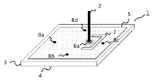
- FIG. It is a perspective view of the composite antenna device which concerns on Embodiment 1.
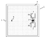
- FIG. It is a top view of the composite antenna device which concerns on Embodiment 1.
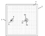
- FIG. It is a bottom view of the composite antenna device which concerns on Embodiment 1.
- FIG. It is sectional drawing in the AA cross section of FIG. It is a top view which shows the example of the hole of the resonance part of the composite antenna device which concerns on Embodiment 1.
- FIG. It is a top view which shows the example of the hole of the resonance part of the composite antenna device which concerns on Embodiment 1.
- FIG. It is a perspective view when the microstrip antenna of the composite antenna apparatus which concerns on Embodiment 1 has a plurality of feeding points.
- FIG. 1 It is a top view when the microstrip antenna of the composite antenna apparatus which concerns on Embodiment 1 has a plurality of feeding points. It is a top view which shows the example of the slit of the resonance part of the composite antenna device which concerns on Embodiment 2.
- FIG. 2 is a top view which shows the example of the slit of the resonance part of the composite antenna device which concerns on Embodiment 2.
- FIG. It is a perspective view of the composite antenna device which concerns on Embodiment 3.
- FIG. It is a top view of the composite antenna device which concerns on Embodiment 3.
- FIG. 5 is a cross-sectional view taken along the line CC of FIG. It is a perspective view when the inverted F antenna is used for the element antenna of the compound antenna apparatus of Embodiment 4.
- FIG. It is a perspective view when the folded antenna is used for the element antenna of the compound antenna apparatus of Embodiment 4.
- FIG. It is a perspective view when the folded monopole antenna and the non-feeding antenna are used for the element antenna of the compound antenna apparatus of Embodiment 4.
- FIG. 5 is a cross-sectional view taken along the line CC of FIG. It is a perspective view when the inverted F antenna is used for the element antenna of the compound antenna apparatus of Embodiment 4.
- FIG. It is a perspective view when the folded antenna is used for the element antenna of the compound antenna apparatus of Embodiment 4.
- FIG. It is a perspective view when the folded monopole antenna and the non-feeding antenna are used for the element antenna of the compound antenna apparatus of Embodiment 4.
- FIG. 1 is a perspective view of the composite antenna device according to the first embodiment, and as shown in the figure, the composite antenna device is mounted on one surface of the first dielectric substrate 3 and the first dielectric substrate 3. It has a ground conductor 4 arranged, a radiating element 5 as a radiating portion arranged on the other surface of the first dielectric substrate 3, a microstrip antenna 1 having a resonance frequency f1, and a first microstrip antenna 1. It includes a monopole antenna 2 having a resonance frequency f2 as a sub-antenna installed on a surface on which the radiating element 5 of one dielectric substrate 3 is arranged. Further, as shown in FIGS.
- this composite antenna device includes an outer conductor 6b that conducts the ground conductor 4 of the microstrip antenna 1 and the radiating element 5, and a monopole antenna 2 surrounded by the outer conductor 6b. It includes a coaxial line 6 having a conducting inner conductor 6a.
- the radiating element 5 in this composite antenna device has a resonance portion 7 that resonates at the resonance frequency f1 of the microstrip antenna 1. As shown in FIGS. 1 and 2, the resonance portion 7 is composed of a U-shaped hole provided in the radiation element 5, and the total length of this hole has a wavelength corresponding to the resonance frequency f1 of the microstrip antenna 1. It is half the length of.
- the first dielectric substrate 3 has a square planar shape.
- the ground conductor 4 is a conductor plate arranged on one surface of the first dielectric substrate 3, and one side is a square having a length of about 1/2 or more of the wavelength corresponding to the resonance frequency f1 of the microstrip antenna 1.
- the radiating element 5 is a conductor plate arranged on the other surface of the first dielectric substrate 3, and is a square having one side having a length of about 1 ⁇ 2 of the wavelength corresponding to the resonance frequency f1 of the microstrip antenna 1. , Conducts from the ground conductor 4 side to the conductor 8 penetrating the first dielectric substrate 3. As shown in FIG. 2, the radiating element 5 is provided with a resonance portion 7 which is a U-shaped hole.
- the hole of the resonance portion 7 has a total length of 1 ⁇ 2 of the wavelength corresponding to the resonance frequency f1 of the microstrip antenna 1 when the U-shape is extended in a straight line. Further, as shown in FIG. 3, a spatial gap is provided between the ground conductor 4 and the conductor 8, and a feeding point for supplying a high frequency signal having a frequency f1 from the conductor 8 to the microstrip antenna is provided between the gaps. 9 is provided.
- the monopole antenna 2 is arranged on the first dielectric substrate 3 on the side where the radiation element 5 of the microstrip antenna 1 is arranged, and has a length of about 1/4 of the wavelength corresponding to the resonance frequency f2.
- a high frequency signal having a frequency f2 is supplied to the monopole antenna 2 via the coaxial line 6.
- the coaxial line 6 is arranged near the center of the resonance portion 7 formed in the radiating element 5.
- the center of the resonance portion 7 is a position half of the total length of the hole of the resonance portion 7 extended in a straight line, that is, a length of 1/4 of the wavelength corresponding to the resonance frequency f1 of the microstrip antenna 1 from the end. Refers to the position of the antenna.
- the inner conductor 6a of the coaxial line 6 conducts with the monopole antenna 2, and the outer conductor 6b conducts with the ground conductor 4 of the microstrip antenna 1 and the radiating element 5.
- the outer conductor 6b may conduct the ground conductor 4 and the radiating element 5 so as to surround the inner conductor 6a by 360 degrees, but if the outer conductor 6a is surrounded by the inner conductor 6a, the outer conductor 6b is alphabetic. It may have a shape like "C".
- the composite antenna device may operate as a receiving antenna.
- the microstrip antenna 1 emits an electromagnetic wave when a high frequency signal having a frequency f1 is supplied from the feeding point 9.
- the monopole antenna 2 radiates an electromagnetic wave when a high frequency signal having a frequency f2 is supplied from the feeding point 10. At this time, the high frequency signal of the frequency f1 supplied to the microstrip antenna 1 resonates at the resonance portion 7 of the microstrip antenna 1.
- the total length of the microstrip antenna is as a resonance portion 7 that resonates with the radiation element 5 constituting the microstrip antenna 1 at the resonance frequency f1 of the microstrip antenna 1. Since a hole having a length of 1/2 of the wavelength corresponding to the resonance frequency f1 of 1 is provided, even when the coaxial line 6 is arranged other than the center of the plane of the microstrip antenna 1, the outer conductor 6b of the coaxial line 6 is provided. The leakage current can be reduced. This makes it possible to combine antennas with improved installation flexibility of sub-antennas such as the monopole antenna 2 without degrading the performance of the microstrip antenna 1.
- the total length of the hole of the resonance portion 7 is not limited to half the length corresponding to the resonance frequency f1 of the microstrip antenna 1, and n / 2 of the wavelength corresponding to the resonance frequency f1 of the microstrip antenna 1. It may be doubled (n is a natural number). In that case, since the current distribution becomes smaller at the position of (2n'-1) / 4 times the wavelength corresponding to the resonance frequency f1 (n'is a natural number) with respect to the total length, the current is coaxial in the vicinity of this. A high effect can be obtained by arranging the line 6.
- the total length of the hole of the resonance portion 7 does not have to be exactly n / 2 times the wavelength, as long as the high frequency signal f1 supplied to the microstrip antenna 1 resonates at the resonance portion 7.
- the shape of the hole of the resonance portion 7 is not limited to the U shape, and may be a swirling shape as shown in FIG. 5, for example. Further, the number of holes is not limited to one, and may be two as shown in FIG.
- FIG. 7 is a perspective view when the microstrip antenna 1 of the composite antenna device according to the first embodiment has a plurality of feeding points 10.
- FIG. 8 is a bottom view when the microstrip antenna 1 of the composite antenna device according to the first embodiment has a plurality of feeding points.
- the conductors 8a, 8b, 8c, and 8d pass through the first dielectric substrate 3 from the direction of the ground conductor 4 and conduct to the radiating element 5. As shown in FIG.
- the phase is 0 degrees at the feeding point 10a of the microstrip antenna, the phase is 270 degrees at the feeding point 10b of the microstrip antenna, the phase is 180 degrees at the feeding point 10c of the microstrip antenna, and the phase is at the feeding point 10d of the microstrip antenna.
- the antenna is right-handed circularly polarized wave (RHCP: Right-Handed Circularly Polarized wave) in the direction in which the radiating element 5 is viewed from the ground conductor 4. Is emitted, and left-handed circularly polarized wave (LHCP) is emitted from the radiating element 5 in the direction in which the ground conductor 4 is viewed. Therefore, the microstrip antenna 1 is also operated as a circularly polarized antenna. Can be done.
- RVCP Right-Handed Circularly Polarized wave
- the resonance portion 7 of the radiation element 5 is a hole, but in the second embodiment, the case where the resonance portion 7 of the radiation element 5 is a slit for making a cut from the end of the radiation element 5 will be described.
- Other configurations are the same as those in the first embodiment.
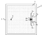
- FIG. 9 is a top view of the composite antenna device according to the second embodiment.
- the radiating element 5 is provided with two linear slits from the end of the radiating element 5 as the resonance portion 7.
- the total length of the slit is about 1/4 of the wavelength corresponding to the resonance frequency f1 of the microstrip antenna 1.
- the resonance portion 7 which is a slit resonates at the resonance frequency f1 of the microstrip antenna 1, and the current increases at the end 7a on the plane center side of the microstrip antenna 1 in the slit, and the plane end side of the microstrip antenna 1 side.
- the current becomes weak. Therefore, since the current is small in the vicinity of the plane end side 7b of the slit, the closer it is, the less the unnecessary leakage current flowing through the outer conductor 6b of the coaxial line 6 can be reduced. The closer the coaxial line 6 is to the end 7b on the plane end side of the resonance portion 7, the more unnecessary leakage current flowing through the outer conductor 6b of the coaxial line 6 can be reduced.
- the total length of the microstrip antenna is as a resonance portion 7 that resonates with the radiation element 5 constituting the microstrip antenna 1 at the resonance frequency f1 of the microstrip antenna 1. Since a slit having a length of 1/4 of the wavelength corresponding to the resonance frequency of 1 is provided, leakage from the outer conductor 6b of the coaxial line 6 even when the coaxial line 6 is arranged outside the center of the plane of the microstrip antenna 1. The current can be reduced. This makes it possible to combine antennas with improved installation flexibility of sub-antennas such as the monopole antenna 2 without degrading the performance of the microstrip antenna 1.
- the total length of the slit of the resonance portion 7 is not limited to 1/4 of the wavelength corresponding to the resonance frequency of the microstrip antenna 1, and 1/4 + (2n ′) of the wavelength corresponding to the resonance frequency of the microstrip antenna 1. -1) / 2 times (n'is a natural number). In this case, since the current weakens at a position (2n-1) / 4 times the wavelength from the end 7a on the plane center side of the slit of the resonance portion 7 on the plane center side, it is expensive to arrange the coaxial line 6 in the vicinity thereof. The effect is obtained.
- the total length of the slit may not be exactly (2n-1) / 4 times the wavelength, but may be a length that resonates with the high frequency signal f1 supplied to the microstrip antenna 1.
- the shape of the slit of the resonance portion 7 is not limited to a linear shape, and may be an L-shape as shown in FIG. 10, for example. Further, the number of slits may be one or two or more.
- Embodiment 3 Next, the composite antenna according to the third embodiment will be described.
- the monopole antenna 2 is arranged directly above the coaxial line 6 penetrating the ground conductor 4 and the first dielectric substrate 3, but in the second embodiment, the monopole antenna 2 is arranged other than directly above the coaxial line 6.
- FIG. 11 is a perspective view of the composite antenna device according to the third embodiment
- FIG. 12 is a top view of FIG. 11
- FIG. 13 is a bottom view of FIG. 11
- FIG. 14 is a cross section taken along the line BB of FIG. It is a figure.
- the inner conductor 6a of the coaxial line 6 penetrates the ground conductor 4 and the first dielectric substrate 3 and then is on the surface of the first dielectric substrate 3 on the side where the radiating element 5 is arranged. It has an extension portion 6c that conducts and extends to the monopole antenna 2.
- the extension portion 6c is a conductor and is arranged on the first dielectric substrate 3.
- the radiating element 5 is provided with a spatial gap so as not to come into contact with the extension portion 6c.
- the inner conductor 6a of the coaxial line 6 and the monopole antenna 2 are conducted on the surface of the first dielectric substrate 3 on the side where the radiating element 5 is arranged. Since the extension portion 6c to be extended is provided, the degree of freedom when arranging the monopole antenna 2 on the surface of the microstrip antenna 1 on the side on which the radiating element 5 is arranged is increased. In particular, by arranging it in the center, the radiating element 5 corresponding to the main plate of the monopole antenna 2 has a structure that contrasts with the horizontal direction, so that the monopole antenna 2 that is almost omnidirectional in the horizontal plane can be obtained. ..
- Embodiment 4 Next, the composite antenna according to the fourth embodiment will be described.
- the composite antenna composed of the microstrip antenna 1 and the monopole antenna 2 has been described, but in the fourth embodiment, the back lobe radiation of the cross-polarization of the circularly polarized antenna as in Patent Document 1 is suppressed.
- the case where the antenna device is used will be described.
- 15 is a perspective view of the composite antenna device according to the fourth embodiment
- FIG. 16 is a top view of FIG.
- FIG. 17 is a bottom view of FIG. 16
- FIG. 18 is a cross section taken along the line CC of FIG. It is a figure.
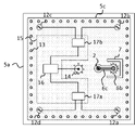
- the composite antenna is composed of a microstrip antenna 1, four element antennas 11 provided on the microstrip antenna 1, and a monopole antenna 2.
- the microstrip antenna 1 is composed of a first dielectric substrate 3, a ground conductor 4, and a radiation portion.
- the radiation portion has a multi-layer structure, and is the other of the second dielectric substrate 5a, the first radiation element 5b arranged on one surface of the second dielectric substrate 5a, and the second dielectric substrate 5a. It has a second radiating element 5c arranged on the surface.
- the second dielectric substrate 5a has a square planar shape.
- the first radiating element 5b and the second radiating element 5c are conductor plates, and one side is a square having a length of about 1/2 wavelength of the resonance frequency f1 of the microstrip antenna 1.
- the first radiating element 5b and the second radiating element 5c are configured to penetrate the second dielectric substrate 5a and be conducted by a plurality of through holes 13.
- the through holes 13 are formed at intervals sufficiently short with respect to the wavelength of the frequency f1 of the high-frequency signal supplied to the microstrip antenna 1, so that the second dielectric substrate 5a, the first radiating element 5b, and the second radiating element are formed.
- the radiation part composed of 5c is made to look like a single metal plate.
- the central coaxial line 14 is provided with a feeding point 18 for supplying high frequency power having a frequency f1 to the microstrip antenna 1.
- the outer conductor 14b of the central coaxial line 14 surrounds the inner conductor 14a with a plurality of conductors, and is electrically connected to the ground conductor 4, the first radiating element 5b, and the second radiating element 5c.
- the interface circuit 15 includes a 180-degree hybrid 16 and 90-degree hybrids 17a and 17b, and is patterned by etching on the second radiating element 5c. Note that the element antennas 11a to 11d are omitted in FIGS. 16 and 18.
- the element antennas 11a, 11b, 11c, 11d and the monopole antenna 2 are arranged on the upper surface of the microstrip antenna 1 on the radiation surface side.
- the element antennas 11a to 11d are L-shaped antennas capable of transmitting and receiving circularly polarized waves.
- the total length of these element antennas 11a to 11d is about 1/4 wavelength of the resonance frequency f1 of the element antennas 11a to 11d.
- the electromagnetic wave radiated in the space is a superposition of the radiation from the element antennas 11a to 11d as the current source and the radiation from the microstrip antenna 1 as the magnetic current source, and is excited by the microstrip antenna 1.
- the element antennas 11a to 11d have feeding points 12a, 12b, 12c, 12d on the second radiating element 5c, but are not formed as physical components.
- the number of element antennas 11a to 11d is not limited to four, and may be any number as long as circularly polarized radiation is possible.
- the operation when the element antennas 11a to 11d are used as the transmitting antenna will be described.
- the operation when the element antennas 11a to 11d are used as the receiving antenna is reversible.
- the phase of the signal output from the central coaxial line 14 to the interface circuit 15 is 0 degrees.
- the 180-degree hybrid 16 of the interface circuit 15 distributes the 0-degree phase signal output from the central coaxial line 14 into two signals having a 180-degree phase difference, and the 0-degree phase signal is a 90-degree hybrid 17a. And outputs a signal with a phase of 180 degrees to the 90 degree hybrid 17b.
- the 90-degree hybrid 17a distributes the 0-degree phase signal output from the 180-degree hybrid 16 to two signals having a 90-degree phase difference, and transfers the 0-degree phase signal to the feeding point 12a of the element antenna 11a. It outputs and outputs a signal having a phase of 90 degrees to the feeding point 12d of the element antenna 11d.
- the 90-degree hybrid 17b distributes the 180-degree phase signal output from the 180-degree hybrid 16 to two signals having a 90-degree phase difference, and transfers the 180-degree phase signal to the feeding point 12c of the element antenna 11c. It outputs and outputs a signal having a phase of 270 degrees to the feeding point 12b of the element antenna 11b.
- the operation of the composite antenna device according to the fourth embodiment will be described.
- the high-frequency signal of frequency f1 supplied to the microstrip antenna 1 resonates at the resonance portion 7 which is a hole. Therefore, a current distribution is obtained in which the current flowing on the surface of the surface of the radiating portion including the first radiating element 5b and the second radiating element 5c increases and the current decreases as it approaches the center of the resonance portion 7.
- the leakage current flowing through the outer conductor 6b of the coaxial line 6 is reduced. Can be done.
- the composite antenna device according to the fourth embodiment is useful when the coaxial line 6 cannot be arranged in the center because the central coaxial line 14 and the interface circuit 15 are provided on the plane of the radiation portion.
- the element antennas 11a to 11d are L-shaped, but antennas having other shapes may be used.
- FIG. 19 is a perspective view when an inverted F antenna is used for the element antennas 11a to 11d of the composite antenna device of the fourth embodiment.
- FIG. 20 is a perspective view when a folded antenna is used for the element antennas 11a to 11d of the composite antenna device of the fourth embodiment.
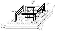
- FIG. 21 is a perspective view in the case where a folded antenna is used for the element antennas 11a to 11d of the composite antenna device of the fourth embodiment and the non-feeding antennas 19a to 19d are used.
- the resonance portion 7 is provided only in the second radiation element 5c, but when the thickness of the first dielectric substrate 3 is thin, the resonance portion 7 which is a hole emits the second radiation. Since it is electromagnetically coupled not only to the element 5c but also to the first radiating element 5b, a desired operation may not be obtained. In that case, the thickness of the first dielectric substrate 3 is increased, or the thickness of the first dielectric substrate 3 remains thin, and the first radiating element 5b and the second radiating element 5c are used. It is desirable to provide resonance portions 7 having the same shape on both. The most effective effect can be obtained by forming the resonance portions 7 of the holes provided in both the first radiating element and the second radiating element so as to face each other.
- FIG. 22 is a diagram showing the relationship between the thickness (t) and the line width (W) of the dielectric substrate when the characteristic impedance of the coplanar line and the coplanar line with GND is 50 [ ⁇ ].
- the frequency is 1.5 [GHz]
- the gap width G is 0.3 [mm]
- the thickness of the copper foil is 18 [ ⁇ m].
- the curves of the CPW having no ground conductor attached to the back surface of the dielectric substrate and the GCPW having the ground conductor attached to the back surface of the dielectric substrate approach each other. This means that by making the dielectric substrate thicker, the electric field formed from the signal line to the ground conductor on the back surface of the dielectric substrate is gradually weakened, and the influence of the ground conductor is reduced. In such a case, since the two curves start to converge, it is considered that the resonance portion 7 can obtain a desired effect if the thickness of the dielectric substrate is set to at least about 2 mm.
- the microstrip antenna 1 may have a multi-layer structure and resonate at f3 which is the third frequency, but in that case, the resonance portion having a total length which resonates at the third frequency f3. It is necessary to newly provide 7. Further, as shown in FIG. 23, notches may be provided on each side of the first radiating element 5b and the second radiating element 5c in order to lower the resonance frequency without increasing the size of the microstrip antenna 1. good. By making the amount of notch provided on each side uniform, the resonance frequency can be shifted to the low frequency range without deteriorating the axial ratio characteristics.
- the non-feeding element 20a for the monopole antenna may be arranged on the radiating element 3 of the microstrip antenna 1.
- FIG. 24 is a perspective view in which one non-feeding element 20a for a monopole antenna is arranged on the radiation element 3 of the microstrip antenna 1 of the present embodiment.
- FIG. 25 is a perspective view in which four non-feeding elements 20a to 20d for a monopole antenna are arranged on the radiation element 5 of the microstrip antenna of the present embodiment.
- the element antennas 19a to 19d are omitted and are not shown.
- the length of the non-feeding element 20a to 20d is set to about 1/4 of the wavelength corresponding to the resonance frequency f2 of the monopole antenna 2, so that the non-feeding element 20a to 20d for the monopole antenna 2 and the monopole antenna is set. Therefore, it is possible to control the directivity and widen the impedance.
- the resonance portion 7 may use either a hole or a slit as long as it resonates at the resonance frequency f1 of the microstrip antenna 1.
- the frequency f1 of the high frequency signal supplied to the microstrip antenna 1 and the frequency f2 of the high frequency signal supplied to the monopole antenna 2 may be the same or different. If the frequencies are the same, it is desirable that each antenna has a low correlation.
- the rectangular microstrip antenna has been described, but the planar shape of the microstrip antenna may be any shape as long as it operates as a microstrip antenna such as a circle.
- the monopole antenna has been described as the sub-antenna, the sub-antenna may be an inverted L-shaped antenna or a helical antenna as long as it is an antenna.
Landscapes
- Waveguide Aerials (AREA)
- Variable-Direction Aerials And Aerial Arrays (AREA)
- Details Of Aerials (AREA)
Abstract
複合アンテナ装置を構成する際は、異なるアンテナシステムが相互干渉を及ぼさないよう考慮し、平面アンテナであるマイクロストリップアンテナとモノポールアンテナを複合したアンテナでは、マイクロストリップアンテナの平面中央では導体間に電界が生じないため、ここに同軸線路を貫通させてモノポールアンテナを配置する。本開示では、共振部を設けることによりマイクロストリップアンテナの平面中央以外に同軸線路を配置した場合にも、同軸線路の外導体からの漏洩電流を低減する複合アンテナ装置を得るものである。
Description
この発明は、複合アンテナ装置に関する。
IOT(Internet Of Things)の普及により、これまで以上にモノがネットワークを通じてサーバやクラウドに接続されることが増えた。そのため通信で用いられるアンテナには小型化だけでなく、多機能化のために複数の通信システムを小さなアンテナに一体化することが要求される。
複合アンテナ装置を構成する際は、異なるアンテナシステムが相互干渉を及ぼさないよう考慮する必要がある。例えば、平面アンテナであるマイクロストリップアンテナとモノポールアンテナを複合したアンテナでは、マイクロストリップアンテナの平面中央では導体間で電界が小さくなるため、ここに同軸線路を貫通させてモノポールアンテナを配置する。このように構成することで、マイクロストリップアンテナの放射特性にほとんど影響を与えることなくアンテナの複合化が可能となる。
特許文献1に開示されたアンテナ装置では、4つの素子アンテナから成る円偏波アンテナの根元に形成された多層基板の内層にマイクロストリップアンテナを挿入することで円偏波アンテナとマイクロストリップアンテナの放射パターンを重ね合わせて、アンテナ後方に放射する交差偏波を抑圧している。
複合アンテナ装置を構成する際は、異なるアンテナシステムが相互干渉を及ぼさないよう考慮する必要がある。例えば、平面アンテナであるマイクロストリップアンテナとモノポールアンテナを複合したアンテナでは、マイクロストリップアンテナの平面中央では導体間で電界が小さくなるため、ここに同軸線路を貫通させてモノポールアンテナを配置する。このように構成することで、マイクロストリップアンテナの放射特性にほとんど影響を与えることなくアンテナの複合化が可能となる。
特許文献1に開示されたアンテナ装置では、4つの素子アンテナから成る円偏波アンテナの根元に形成された多層基板の内層にマイクロストリップアンテナを挿入することで円偏波アンテナとマイクロストリップアンテナの放射パターンを重ね合わせて、アンテナ後方に放射する交差偏波を抑圧している。
このようなアンテナ装置では、4つの素子アンテナに電力を供給する目的で内層にマイクロストリップアンテナを形成した多層基板内部を貫通するスルーホールが基板中央付近にあるため、マイクロストリップアンテナの平面中央に給電用の同軸線路を配置することができない。しかし、マイクロストリップアンテナの平面中央以外の位置に同軸線路を貫通させて配置すると、外導体によりマイクロストリップアンテナの導体間が短絡し電流が漏洩してしまう。これによりマイクロストリップアンテナ内部の電界分布に影響を与え、放射特性が変化してしまうという問題があった。
本開示は、上記の問題を解決するためになされたものであり、マイクロストリップアンテナの平面中央以外に同軸線路を配置した場合に、同軸線路の外導体からの漏洩電流を低減する複合アンテナ装置を得るものである。
本開示に係る複合アンテナは、誘電体基板、誘電体基板の一方の面に配置された地導体、誘電体基板の他方の面に配置された放射部を有するマイクロストリップアンテナと、誘電体基板において放射部が配置される面上に配置されるサブアンテナと、地導体と放射部とを導通する外導体、外導体に囲まれサブアンテナと導通する内導体とを有する同軸線路とを備え、放射部は、マイクロストリップアンテナに給電される高周波信号が共振する共振部を有するものである。
本開示によれば、マイクロストリップアンテナを構成する放射部はマイクロストリップアンテナに給電される高周波信号が共振する共振部を有するので、マイクロストリップアンテナの平面中央以外に同軸線路を配置した場合にも同軸線路の外導体からの漏洩電流を低減することができる。
実施の形態1.
以下、実施の形態1に係る複合アンテナ装置について説明する。
図1は、本実施の形態1に係る複合アンテナ装置の斜視図であり、図に示すように複合アンテナ装置は、第一の誘電体基板3、第一の誘電体基板3の一方の面に配置された地導体4、第一の誘電体基板3の他方の面に配置された放射部としての放射素子5とを有し、共振周波数f1のマイクロストリップアンテナ1と、マイクロストリップアンテナ1の第一の誘電体基板3の放射素子5が配置される面上に設置されるサブアンテナとしての共振周波数f2のモノポールアンテナ2とを備えている。
また、図2から図4に示すように、この複合アンテナ装置は、マイクロストリップアンテナ1の地導体4と放射素子5とを導通する外導体6b、前記外導体6bに囲まれモノポールアンテナ2と導通する内導体6aとを有する同軸線路6とを備えている。
そして、この複合アンテナ装置における放射素子5は、マイクロストリップアンテナ1の共振周波数f1で共振する共振部7を有している。この共振部7は図1~2に示すように、放射素子5に設けられたコの字状の穴で構成されており、この穴の全長はマイクロストリップアンテナ1の共振周波数f1に対応した波長の1/2の長さとなっている。
以下、実施の形態1に係る複合アンテナ装置について説明する。
図1は、本実施の形態1に係る複合アンテナ装置の斜視図であり、図に示すように複合アンテナ装置は、第一の誘電体基板3、第一の誘電体基板3の一方の面に配置された地導体4、第一の誘電体基板3の他方の面に配置された放射部としての放射素子5とを有し、共振周波数f1のマイクロストリップアンテナ1と、マイクロストリップアンテナ1の第一の誘電体基板3の放射素子5が配置される面上に設置されるサブアンテナとしての共振周波数f2のモノポールアンテナ2とを備えている。
また、図2から図4に示すように、この複合アンテナ装置は、マイクロストリップアンテナ1の地導体4と放射素子5とを導通する外導体6b、前記外導体6bに囲まれモノポールアンテナ2と導通する内導体6aとを有する同軸線路6とを備えている。
そして、この複合アンテナ装置における放射素子5は、マイクロストリップアンテナ1の共振周波数f1で共振する共振部7を有している。この共振部7は図1~2に示すように、放射素子5に設けられたコの字状の穴で構成されており、この穴の全長はマイクロストリップアンテナ1の共振周波数f1に対応した波長の1/2の長さとなっている。
より詳細に説明すると、第一の誘電体基板3は、正方形の平面形状である。地導体4は、第一の誘電体基板3の一方の面に配置される導体板で、一辺はマイクロストリップアンテナ1の共振周波数f1に対応する波長の約1/2以上の長さの正方形である。放射素子5は、第一の誘電体基板3の他方の面に配置される導体板で、一辺がマイクロストリップアンテナ1の共振周波数f1に対応する波長の約1/2の長さの正方形であり、地導体4側から第一の誘電体基板3を貫通した導体8と導通している。図2に示すように、放射素子5には、コの字状の穴である共振部7が設けられている。共振部7の穴は、コの字を一直線に伸ばした際の全長がマイクロストリップアンテナ1の共振周波数f1に対応する波長の1/2の長さを有する。また、図3に示すように、地導体4と導体8の間には空間的なギャップを設けられ、ギャップ間には導体8からマイクロストリップアンテナに周波数f1の高周波信号を供給するための給電点9が設けられている。
モノポールアンテナ2は、マイクロストリップアンテナ1の放射素子5が配置される側の第一の誘電体基板3上に配置され、共振周波数f2に対応する波長の約1/4の長さを有する。モノポールアンテナ2には、同軸線路6を経由して周波数f2の高周波信号が供給される。図2に示すように、同軸線路6は放射素子5に形成された共振部7の中央近傍に配置される。ここで共振部7の中央とは、共振部7の穴を一直線に伸ばした全長に対して半分の位置、すなわち、端からマイクロストリップアンテナ1の共振周波数f1に対応する波長の1/4の長さの位置を指す。同軸線路6の内導体6aはモノポールアンテナ2と導通し、外導体6bはマイクロストリップアンテナ1の地導体4と放射素子5とを導通する。外導体6bは、図3に示すように、内導体6aを360度囲むようにして地導体4と放射素子5とを導通させても良いが、内導体6aを囲むようにすれば外導体6bがアルファベットの「C」のような形状でも良い。マイクロストリップアンテナ1の給電点9と同様に同軸線路6の内導体6aと地導体4の間には空間的なギャップが存在し、ギャップ間にはモノポールアンテナ2に周波数f2の高周波信号を供給するための給電点10を有する。
次に、本実施の形態1に係る複合アンテナ装置の動作について説明する。本実施の形態では、複合アンテナ装置が送信アンテナとして動作する場合について説明するが、複合アンテナ装置は受信アンテナとして動作するものであっても良い。
マイクロストリップアンテナ1は、給電点9から周波数f1の高周波信号が供給されると電磁波が放射される。モノポールアンテナ2は、給電点10から周波数f2の高周波信号が供給されると電磁波を放射する。
この時、マイクロストリップアンテナ1の共振部7にて、マイクロストリップアンテナ1に供給した周波数f1の高周波信号が共振する。このため、共振部7の端部付近では放射素子5の表面を流れる電流が大きくなり、共振部7の中央に近づくにつれて電流が小さくなる電流分布が得られる。このように、マイクロストリップアンテナ1の共振周波数f1において放射素子5の表面に形成された共振部7の端部に電流を集中させることで、同軸線路6の外導体6bを流れる漏洩電流を小さくすることができる。なお、同軸線路6は共振部7の中央に近ければ近いほど、同軸線路6の外導体6bを流れる不要な漏洩電流を低減することができる。
マイクロストリップアンテナ1は、給電点9から周波数f1の高周波信号が供給されると電磁波が放射される。モノポールアンテナ2は、給電点10から周波数f2の高周波信号が供給されると電磁波を放射する。
この時、マイクロストリップアンテナ1の共振部7にて、マイクロストリップアンテナ1に供給した周波数f1の高周波信号が共振する。このため、共振部7の端部付近では放射素子5の表面を流れる電流が大きくなり、共振部7の中央に近づくにつれて電流が小さくなる電流分布が得られる。このように、マイクロストリップアンテナ1の共振周波数f1において放射素子5の表面に形成された共振部7の端部に電流を集中させることで、同軸線路6の外導体6bを流れる漏洩電流を小さくすることができる。なお、同軸線路6は共振部7の中央に近ければ近いほど、同軸線路6の外導体6bを流れる不要な漏洩電流を低減することができる。
以上のように、本実施の形態1に係る複合アンテナ装置によれば、マイクロストリップアンテナ1を構成する放射素子5にマイクロストリップアンテナ1の共振周波数f1で共振する共振部7として全長がマイクロストリップアンテナ1の共振周波数f1に対応する波長の1/2の長さの穴を設けたので、マイクロストリップアンテナ1の平面中央以外に同軸線路6を配置した場合にも同軸線路6の外導体6bからの漏洩電流を低減することができる。これにより、マイクロストリップアンテナ1の性能を劣化させることなく、モノポールアンテナ2のようなサブアンテナの設置自由度を改善したアンテナの複合化が可能となる。
なお、共振部7の穴の全長はマイクロストリップアンテナ1の共振周波数f1に対応する長さの1/2の長さに限らず、マイクロストリップアンテナ1の共振周波数f1に対応する波長のn/2倍(nは自然数)であればよい。その場合、全長に対して共振周波数f1に対応する波長の(2n′-1)/4倍(n′は自然数)の長さの位置に電流が小さくなる電流分布となるため、この付近に同軸線路6を配置すると高い効果が得られる。また、共振部7の穴の全長は厳密に波長のn/2倍でなくとも、マイクロストリップアンテナ1に供給する高周波信号f1が共振部7にて共振する長さであればよい。共振部7の穴の形状もコの字状に限られるものではなく、例えば図5に示されるように渦を巻く形状でも良い。また、穴の個数も1つに限定されるものではなく、図6に示されるように2つあっても良い。
また、マイクロストリップアンテナ1の給電点9と放射素子5をつなぐ導体8は1つに限らず複数設けても良い。図7は、本実施の形態1に係る複合アンテナ装置のマイクロストリップアンテナ1が複数の給電点10を有する場合の斜視図である。図8は本実施の形態1に係る複合アンテナ装置のマイクロストリップアンテナ1が複数の給電点を有する場合の下面図である。導体8a、8b、8c、8dは、地導体4の方向から第一の誘電体基板3を貫通して放射素子5に導通している。図8に示すように、地導体4と導体8a、8b、8c、8dの間には空間的なギャップが存在し、ギャップ間にはマイクロストリップアンテナに周波数f1の高周波信号を供給するための給電点10a、10b、10c、10dを有している。
例えば、マイクロストリップアンテナの給電点10aに位相が0度、マイクロストリップアンテナの給電点10bに位相が270度、マイクロストリップアンテナの給電点10cに位相が180度、マイクロストリップアンテナの給電点10dに位相が90度のように互いに位相が90度ずつ異なり、振幅が等しい高周波信号を与えれば、地導体4から放射素子5を見た方向に右旋円偏波(RHCP:Right-Handed Circularly Polarized wave)が放射され、放射素子5から地導体4を見た方向に左旋円偏波(LHCP:Left-Handed Circularly Polarized wave)が放射されるため、マイクロストリップアンテナ1を円偏波アンテナとしても動作させることができる。
例えば、マイクロストリップアンテナの給電点10aに位相が0度、マイクロストリップアンテナの給電点10bに位相が270度、マイクロストリップアンテナの給電点10cに位相が180度、マイクロストリップアンテナの給電点10dに位相が90度のように互いに位相が90度ずつ異なり、振幅が等しい高周波信号を与えれば、地導体4から放射素子5を見た方向に右旋円偏波(RHCP:Right-Handed Circularly Polarized wave)が放射され、放射素子5から地導体4を見た方向に左旋円偏波(LHCP:Left-Handed Circularly Polarized wave)が放射されるため、マイクロストリップアンテナ1を円偏波アンテナとしても動作させることができる。
実施の形態2.
次に、実施の形態2に係る複合アンテナについて説明する。実施の形態1では、放射素子5の共振部7は穴であったが、実施の形態2では放射素子5の共振部7が放射素子5の端から切込みを入れるスリットである場合について説明する。その他の構成は実施の形態1と同様である。
次に、実施の形態2に係る複合アンテナについて説明する。実施の形態1では、放射素子5の共振部7は穴であったが、実施の形態2では放射素子5の共振部7が放射素子5の端から切込みを入れるスリットである場合について説明する。その他の構成は実施の形態1と同様である。
図9は、実施の形態2に係る複合アンテナ装置の上面図である。図9に示すように放射素子5には、放射素子5の端部から2つの直線状のスリットを共振部7として設けられている。スリットは、全長がマイクロストリップアンテナ1の共振周波数f1に対応する波長の約1/4の長さである。
次に、本実施の形態2に係る複合アンテナ装置の動作について説明する。マイクロストリップアンテナ1は、マイクロストリップアンテナ1の給電点10から供給された高周波信号が導体8を経由して放射素子5に与えられると電磁波が空間に放射される。この時、スリットである共振部7はマイクロストリップアンテナ1の共振周波数f1で共振し、スリットにおいてマイクロストリップアンテナ1の平面中央側の端7aでは電流が大きくなり、マイクロストリップアンテナ1の平面端部側の端7bでは電流が弱くなる。従って、スリットの平面端部側7b近傍では電流が小さいため、そこに近ければ近いほど同軸線路6の外導体6bに流れる不要な漏洩電流を低減することができる。なお、同軸線路6は共振部7の平面端部側の端7bに近ければ近いほど、同軸線路6の外導体6bを流れる不要な漏洩電流を低減することができる。
次に、本実施の形態2に係る複合アンテナ装置の動作について説明する。マイクロストリップアンテナ1は、マイクロストリップアンテナ1の給電点10から供給された高周波信号が導体8を経由して放射素子5に与えられると電磁波が空間に放射される。この時、スリットである共振部7はマイクロストリップアンテナ1の共振周波数f1で共振し、スリットにおいてマイクロストリップアンテナ1の平面中央側の端7aでは電流が大きくなり、マイクロストリップアンテナ1の平面端部側の端7bでは電流が弱くなる。従って、スリットの平面端部側7b近傍では電流が小さいため、そこに近ければ近いほど同軸線路6の外導体6bに流れる不要な漏洩電流を低減することができる。なお、同軸線路6は共振部7の平面端部側の端7bに近ければ近いほど、同軸線路6の外導体6bを流れる不要な漏洩電流を低減することができる。
以上のように、本実施の形態2に係る複合アンテナ装置によれば、マイクロストリップアンテナ1を構成する放射素子5にマイクロストリップアンテナ1の共振周波数f1で共振する共振部7として全長がマイクロストリップアンテナ1の共振周波数に対応する波長の1/4の長さのスリットを設けたので、マイクロストリップアンテナ1の平面中央以外に同軸線路6を配置した場合にも同軸線路6の外導体6bからの漏洩電流を低減することができる。これにより、マイクロストリップアンテナ1の性能を劣化させることなく、モノポールアンテナ2のようなサブアンテナの設置自由度を改善したアンテナの複合化が可能となる。
なお、共振部7のスリットの全長はマイクロストリップアンテナ1の共振周波数に対応する波長の1/4の長さに限らず、マイクロストリップアンテナ1の共振周波数に対応する波長の1/4+(2n′-1)/2倍(n′は自然数)であればよい。この場合、共振部7のスリットのマイクロストリップアンテナ1の平面中央側の端7aから波長の(2n-1)/4倍の位置において電流が弱くなるため、この付近に同軸線路6を配置すると高い効果が得られる。また、スリットの全長は厳密に波長の(2n-1)/4倍でなくともマイクロストリップアンテナ1に供給する高周波信号f1が共振する長さであればよい。共振部7のスリットの形状も直線状に限定されるものではなく、例えば図10に示されるようにL字形状でも良い。また、スリットの数は1つでも2つ以上でも良い。
実施の形態3.
次に、実施の形態3に係る複合アンテナについて説明する。実施の形態1では、地導体4及び第一の誘電体基板3を貫通した同軸線路6の真上にモノポールアンテナ2を配置したが、実施の形態2では同軸線路6の真上以外にモノポールアンテナ2を配置する場合について説明する。その他は実施の形態1と同様である。
図11は、本実施の形態3に係る複合アンテナ装置の斜視図であり、図12は図11の上面図、図13は図11の下面図、図14は図11のB-B断面における断面図である。
次に、実施の形態3に係る複合アンテナについて説明する。実施の形態1では、地導体4及び第一の誘電体基板3を貫通した同軸線路6の真上にモノポールアンテナ2を配置したが、実施の形態2では同軸線路6の真上以外にモノポールアンテナ2を配置する場合について説明する。その他は実施の形態1と同様である。
図11は、本実施の形態3に係る複合アンテナ装置の斜視図であり、図12は図11の上面図、図13は図11の下面図、図14は図11のB-B断面における断面図である。
図11に示すように、同軸線路6の内導体6aは、地導体4及び第一の誘電体基板3を貫通後、第一の誘電体基板3の放射素子5が配置される側の面上でモノポールアンテナ2まで導通させて延長する延長部6cを有する。延長部6cは、導体であり、第一の誘電体基板3上に配置される。図12に示すように、放射素子5は延長部6cと接触しないよう空間的なギャップが設けられている。
以上のように、実施の形態3に係る複合アンテナ装置は第一の誘電体基板3の放射素子5が配置される側の面上で同軸線路6の内導体6aとモノポールアンテナ2とを導通させて延長する延長部6cを有するので、マイクロストリップアンテナ1の放射素子5が配置される側の面上にモノポールアンテナ2を配置する際の自由度が増える。特に中央に配置することによりモノポールアンテナ2の地板に該当する放射素子5が水平方向に対して対照的な構造となるため、水平面内において概ね無指向となるモノポールアンテナ2を得ることができる。
実施の形態4.
次に、実施の形態4に係る複合アンテナについて説明する。実施の形態1ではマイクロストリップアンテナ1とモノポールアンテナ2から構成される複合アンテナについて説明したが、実施の形態4では特許文献1のような円偏波アンテナの交差偏波のバックローブ放射を抑圧するアンテナ装置を用いる場合について説明する。
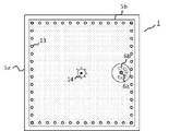
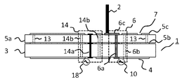
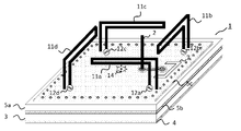
図15は、本実施の形態4に係る複合アンテナ装置の斜視図であり、図16は図15の上面図、図17は図16の下面図、図18は図15のC-C断面における断面図である。複合アンテナは、マイクロストリップアンテナ1と、マイクロストリップアンテナ1上に設けられた4つの素子アンテナ11とモノポールアンテナ2から構成される。
次に、実施の形態4に係る複合アンテナについて説明する。実施の形態1ではマイクロストリップアンテナ1とモノポールアンテナ2から構成される複合アンテナについて説明したが、実施の形態4では特許文献1のような円偏波アンテナの交差偏波のバックローブ放射を抑圧するアンテナ装置を用いる場合について説明する。
図15は、本実施の形態4に係る複合アンテナ装置の斜視図であり、図16は図15の上面図、図17は図16の下面図、図18は図15のC-C断面における断面図である。複合アンテナは、マイクロストリップアンテナ1と、マイクロストリップアンテナ1上に設けられた4つの素子アンテナ11とモノポールアンテナ2から構成される。
マイクロストリップアンテナ1は、第一の誘電体基板3、地導体4、放射部から構成される。放射部は多層構造となっており、第二の誘電体基板5a、第二の誘電体基板5aの一方の面に配置された第一の放射素子5b、第二の誘電体基板5aの他方の面に配置された第二の放射素子5cを有する。第二の誘電体基板5aは、正方形の平面形状である。第一の放射素子5bと第二の放射素子5cは導体板で、一辺がマイクロストリップアンテナ1の共振周波数f1の約1/2波長の長さの正方形である。第一の放射素子5bと第二の放射素子5cは第二の誘電体基板5aを貫通して複数のスルーホール13で導通されるように構成されている。スルーホール13はマイクロストリップアンテナ1に供給する高周波信号の周波数f1の波長に対して十分短い間隔で形成することで、第二の誘電体基板5a、第一の放射素子5b、第二の放射素子5cから構成される放射部を一枚の金属板のように見えるようにしている。
マイクロストリップアンテナ1の平面中央には、第一の誘電体基板3、地導体4、第一の放射素子5b、第二の誘電体基板5a、第二の放射素子5cを貫通する中央同軸線路14が配置される。図18に示すように、中央同軸線路14には、マイクロストリップアンテナ1に周波数f1の高周波電力を供給するための給電点18が設けられている。中央同軸線路14の外導体14bは複数の導体にて内導体14aを囲み、地導体4、第一の放射素子5b、第二の放射素子5cと導通している。第二の放射素子5c側の内導体14aの一端は、図16にて点線で囲まれるインタフェース回路15と接続される。インタフェース回路15は、180度ハイブリッド16及び90度ハイブリッド17a、17bを備え、第二の放射素子5c上にエッチングでパターン形成されている。なお、図16及び図18にて素子アンテナ11a~11dは省略されている。
マイクロストリップアンテナ1の放射面側の上面には、素子アンテナ11a、11b、11c、11dとモノポールアンテナ2が配置される。
素子アンテナ11a~11dは、円偏波を送受信可能なL字状のアンテナである。これらの素子アンテナ11a~11dの全長は、素子アンテナ11a~11dの共振周波数f1の1/4波長程度の長さである。素子アンテナ11a~11dと、マイクロストリップアンテナ1の共振周波数を合わせることで、素子アンテナ11a~11dから発生する電磁波が、マイクロストリップアンテナ1と電磁結合し、マイクロストリップアンテナ1からも電磁波が放射される。この時、空間に放射される電磁波は、電流源となる素子アンテナ11a~11dからの放射と、磁流源となるマイクロストリップアンテナ1からの放射の重ね合わせとなり、マイクロストリップアンテナ1に励振される電力の振幅と位相を適切に調整することでアンテナ背面に放射される交差偏波(不要波)が打ち消しあう関係性が得られる。
素子アンテナ11a~11dは、第二の放射素子5c上に給電点12a、12b、12c、12dを有するが、物理的な構成要素として形成されるわけではない。なお、素子アンテナ11a~11dの数は4つに限られず、円偏波放射が可能であればいくつでも良い。
素子アンテナ11a~11dは、円偏波を送受信可能なL字状のアンテナである。これらの素子アンテナ11a~11dの全長は、素子アンテナ11a~11dの共振周波数f1の1/4波長程度の長さである。素子アンテナ11a~11dと、マイクロストリップアンテナ1の共振周波数を合わせることで、素子アンテナ11a~11dから発生する電磁波が、マイクロストリップアンテナ1と電磁結合し、マイクロストリップアンテナ1からも電磁波が放射される。この時、空間に放射される電磁波は、電流源となる素子アンテナ11a~11dからの放射と、磁流源となるマイクロストリップアンテナ1からの放射の重ね合わせとなり、マイクロストリップアンテナ1に励振される電力の振幅と位相を適切に調整することでアンテナ背面に放射される交差偏波(不要波)が打ち消しあう関係性が得られる。
素子アンテナ11a~11dは、第二の放射素子5c上に給電点12a、12b、12c、12dを有するが、物理的な構成要素として形成されるわけではない。なお、素子アンテナ11a~11dの数は4つに限られず、円偏波放射が可能であればいくつでも良い。
ここで、素子アンテナ11a~11dが送信アンテナとして用いられる場合の動作について説明する。なお、素子アンテナ11a~11dが受信アンテナとして用いられる場合の動作とは可逆的である。
ここでは、説明の便宜上、中央同軸線路14からインタフェース回路15に出力される信号の位相が0度であるものとする。
インタフェース回路15の180度ハイブリッド16は、中央同軸線路14から出力された位相が0度の信号を、位相が180度異なる2つの信号に分配して、位相が0度の信号を90度ハイブリッド17aに出力し、位相が180度の信号を90度ハイブリッド17bに出力する。
90度ハイブリッド17aは、180度ハイブリッド16から出力された位相が0度の信号を、位相が90度異なる2つの信号に分配して、位相が0度の信号を素子アンテナ11aの給電点12aに出力し、位相が90度の信号を素子アンテナ11dの給電点12dに出力する。
90度ハイブリッド17bは、180度ハイブリッド16から出力された位相が180度の信号を、位相が90度異なる2つの信号に分配して、位相が180度の信号を素子アンテナ11cの給電点12cに出力し、位相が270度の信号を素子アンテナ11bの給電点12bに出力する。
これにより、素子アンテナ11a~11dには、互いに位相が90度ずつ異なる信号が与えられ、信号が素子アンテナ11a~11dを伝わる際に生じる共振現象によって、信号に対応する電磁波が空間に放射される。
この場合、素子アンテナ11a~11dを伝わる信号の位相が、互いに90度ずつ異なっているため、右旋円偏波が地導体4から第二の放射素子5cを見た方向に放射される。
また、90度ハイブリッド17a、17bから出力される位相を反対にすることで左旋円偏波を地導体4から第二の放射素子5cを見た方向に放射することも可能である。
ここでは、説明の便宜上、中央同軸線路14からインタフェース回路15に出力される信号の位相が0度であるものとする。
インタフェース回路15の180度ハイブリッド16は、中央同軸線路14から出力された位相が0度の信号を、位相が180度異なる2つの信号に分配して、位相が0度の信号を90度ハイブリッド17aに出力し、位相が180度の信号を90度ハイブリッド17bに出力する。
90度ハイブリッド17aは、180度ハイブリッド16から出力された位相が0度の信号を、位相が90度異なる2つの信号に分配して、位相が0度の信号を素子アンテナ11aの給電点12aに出力し、位相が90度の信号を素子アンテナ11dの給電点12dに出力する。
90度ハイブリッド17bは、180度ハイブリッド16から出力された位相が180度の信号を、位相が90度異なる2つの信号に分配して、位相が180度の信号を素子アンテナ11cの給電点12cに出力し、位相が270度の信号を素子アンテナ11bの給電点12bに出力する。
これにより、素子アンテナ11a~11dには、互いに位相が90度ずつ異なる信号が与えられ、信号が素子アンテナ11a~11dを伝わる際に生じる共振現象によって、信号に対応する電磁波が空間に放射される。
この場合、素子アンテナ11a~11dを伝わる信号の位相が、互いに90度ずつ異なっているため、右旋円偏波が地導体4から第二の放射素子5cを見た方向に放射される。
また、90度ハイブリッド17a、17bから出力される位相を反対にすることで左旋円偏波を地導体4から第二の放射素子5cを見た方向に放射することも可能である。
次に実施の形態4に係る複合アンテナ装置の動作について説明する。
マイクロストリップアンテナ1及びモノポールアンテナ2に高周波信号が給電されると、穴である共振部7にてマイクロストリップアンテナ1に供給した周波数f1の高周波信号が共振する。このため、第一の放射素子5bと第二の放射素子5cからなる放射部の表面の表面を流れる電流が大きくなり、共振部7の中央に近づくにつれて電流が小さくなる電流分布が得られる。このように、マイクロストリップアンテナ1の共振周波数f1において放射部の表面に形成された共振部7の端部に電流を集中させることで、同軸線路6の外導体6bを流れる漏洩電流を小さくすることができる。
マイクロストリップアンテナ1及びモノポールアンテナ2に高周波信号が給電されると、穴である共振部7にてマイクロストリップアンテナ1に供給した周波数f1の高周波信号が共振する。このため、第一の放射素子5bと第二の放射素子5cからなる放射部の表面の表面を流れる電流が大きくなり、共振部7の中央に近づくにつれて電流が小さくなる電流分布が得られる。このように、マイクロストリップアンテナ1の共振周波数f1において放射部の表面に形成された共振部7の端部に電流を集中させることで、同軸線路6の外導体6bを流れる漏洩電流を小さくすることができる。
以上のように、実施の形態4に係る複合アンテナ装置は、放射部の平面に中央同軸線路14やインタフェース回路15が設けられたことにより同軸線路6を中央に配置できない場合に有用である。
なお、実施の形態4では素子アンテナ11a~11dはL字状のものを用いたが、他の形状のアンテナでも良い。図19は、本実施の形態4の複合アンテナ装置の素子アンテナ11a~11dに逆Fアンテナを用いた場合の斜視図である。図20は、本実施の形態4の複合アンテナ装置の素子アンテナ11a~11dに折り返しアンテナを用いた場合の斜視図である。
図21は、本実施の形態4の複合アンテナ装置の素子アンテナ11a~11dに折り返しアンテナを用い、さらに無給電アンテナ19a~19dを用いた場合の斜視図である。無給電アンテナ19a~19dを設けることで素子アンテナである折り返しアンテナ11a~11dとの電磁結合により、第3の周波数となるf3で共振が発生して円偏波特性を得ることができる。
図21は、本実施の形態4の複合アンテナ装置の素子アンテナ11a~11dに折り返しアンテナを用い、さらに無給電アンテナ19a~19dを用いた場合の斜視図である。無給電アンテナ19a~19dを設けることで素子アンテナである折り返しアンテナ11a~11dとの電磁結合により、第3の周波数となるf3で共振が発生して円偏波特性を得ることができる。
また、実施の形態4では第二の放射素子5cのみに共振部7を設けたが、第一の誘電体基板3の厚さが薄い場合には、穴である共振部7が第二の放射素子5cだけでなく第一の放射素子5bと電磁結合するため、所望の動作が得られない場合がある。その場合には、第一の誘電体基板3の厚さを厚くするか、もしくは第一の誘電体基板3の厚さが薄いままで、第一の放射素子5bと第二の放射素子5cの両方に同一形状の共振部7を設けることが望ましい。第一の放射素子と第二の放射素子の両方に設ける穴の共振部7は対面するように形成することで最も効果が得られる。
第一の誘電体基板3の厚さを決定するための一例として、コプレーナ線路(CPW)とGND付きコプレーナ線路(GCPW)の特性インピーダンスが50[Ω]となる時の各線路の誘電体基板の厚さ(t)と線幅(W)の関係について示す。
図22は、コプレーナ線路とGND付コプレーナ線路の特性インピーダンスが50[Ω]となる時の誘電体基板の厚さ(t)と線幅(W)の関係を表した図である。ここでは、周波数を1.5[GHz]、ギャップ幅Gを0.3[mm]、銅箔の厚さを18[μm]としている。
誘電体基板の厚さを厚くするにつれて、誘電体基板の背面に地導体が付与されていないCPWと、誘電体基板の背面に地導体が付与されているGCPWの曲線が互いに近づく。これは、誘電体基板を厚くすることで信号線から誘電体基板の背面にある地導体に形成される電界が徐々に弱くなり、地導体の影響を受けにくくなっていることを意味する。このような場合には、2つの曲線が収束し始めることから、誘電体基板の厚さを最低でも2mm程度にすれば共振部7は所望の効果が得られると考えられる。
図22は、コプレーナ線路とGND付コプレーナ線路の特性インピーダンスが50[Ω]となる時の誘電体基板の厚さ(t)と線幅(W)の関係を表した図である。ここでは、周波数を1.5[GHz]、ギャップ幅Gを0.3[mm]、銅箔の厚さを18[μm]としている。
誘電体基板の厚さを厚くするにつれて、誘電体基板の背面に地導体が付与されていないCPWと、誘電体基板の背面に地導体が付与されているGCPWの曲線が互いに近づく。これは、誘電体基板を厚くすることで信号線から誘電体基板の背面にある地導体に形成される電界が徐々に弱くなり、地導体の影響を受けにくくなっていることを意味する。このような場合には、2つの曲線が収束し始めることから、誘電体基板の厚さを最低でも2mm程度にすれば共振部7は所望の効果が得られると考えられる。
実施の形態4に限らず、マイクロストリップアンテナ1は多層構造にして、第3の周波数となるf3で共振させても良いが、その場合には第3の周波数f3で共振する全長を有する共振部7を新たに設ける必要がある。
また、マイクロストリップアンテナ1を大型化することなく,共振周波数を低くするために図23に示すように第一の放射素子5bと第二の放射素子5cの各辺上に切り欠きを設けても良い。各辺に設ける切欠き量は均一にすることで軸比特性を劣化させることなく,共振周波数を低域にシフトさせることができる。
また、マイクロストリップアンテナ1を大型化することなく,共振周波数を低くするために図23に示すように第一の放射素子5bと第二の放射素子5cの各辺上に切り欠きを設けても良い。各辺に設ける切欠き量は均一にすることで軸比特性を劣化させることなく,共振周波数を低域にシフトさせることができる。
また、 マイクロストリップアンテナ1の放射素子3上にモノポールアンテナ用の無給電素子20aを配置させても良い。図24は、本実施の形態のマイクロストリップアンテナ1の放射素子3上にモノポールアンテナ用の無給電素子20aを1つ配置した斜視図である。図25は、本実施の形態のマイクロストリップアンテナの放射素子5上にモノポールアンテナ用の無給電素子20a~20dを4つ配置した斜視図である。図24と図25において素子アンテナ19a~19dは省略され、図示されていない。
無給電素子20a~20dの長さは、モノポールアンテナ2の共振周波数f2に対応する波長の1/4程度の長さとすることでモノポールアンテナ2とモノポールアンテナ用の無給電素子20a~20dが結合するため、指向性の制御やインピーダンスの広帯域化が可能となる。
無給電素子20a~20dの長さは、モノポールアンテナ2の共振周波数f2に対応する波長の1/4程度の長さとすることでモノポールアンテナ2とモノポールアンテナ用の無給電素子20a~20dが結合するため、指向性の制御やインピーダンスの広帯域化が可能となる。
なお、全ての実施の形態において、共振部7はマイクロストリップアンテナ1の共振周波数f1で共振させるものであれば穴とスリットどちらを用いてもよい。
また、マイクロストリップアンテナ1に供給する高周波信号の周波数f1とモノポールアンテナ2に供給する高周波信号の周波数f2は同じでも良いし、異なっていても良い。同じ周波数とする場合は、各アンテナが低相関であることが望ましい。
また、上述した実施の形態では矩形状のマイクロストリップアンテナを用いて説明したが、マイクロストリップアンテナの平面形状は円形などマイクロストリップアンテナとして動作するものであればどのような形状でも良い。
また、サブアンテナにモノポールアンテナを用いて説明したが、サブアンテナはアンテナであれば逆L字アンテナやヘリカルアンテナなどでも良い。
また、マイクロストリップアンテナ1に供給する高周波信号の周波数f1とモノポールアンテナ2に供給する高周波信号の周波数f2は同じでも良いし、異なっていても良い。同じ周波数とする場合は、各アンテナが低相関であることが望ましい。
また、上述した実施の形態では矩形状のマイクロストリップアンテナを用いて説明したが、マイクロストリップアンテナの平面形状は円形などマイクロストリップアンテナとして動作するものであればどのような形状でも良い。
また、サブアンテナにモノポールアンテナを用いて説明したが、サブアンテナはアンテナであれば逆L字アンテナやヘリカルアンテナなどでも良い。
1.マイクロストリップアンテナ
2.モノポールアンテナ
3.第一の誘電体基板
4.地導体
5.放射素子
5a.第二の誘電体基板
5b.第一の放射素子
5c.第二の放射素子
6.同軸線路
6a.同軸線路の内導体
6b.同軸線路の外導体
6c.延長部
7.共振部
7a.マイクロストリップアンテナの平面中央側の共振部端部
7b.マイクロストリップアンテナの平面端部側の共振部端部
8.8a.8b.8c.8d.導体
9.10.12.18.給電点
11a.11b.11c.11d.素子アンテナ
13.スルーホール
14.中央同軸線路
14a.中央同軸線路の内導体
14b.中央同軸線路の外導体
15.インタフェース回路
16.180度ハイブリッド
17.90度ハイブリッド
19a.19b.19c.19d.無給電アンテナ
20a.20b.20c.20d.無給電素子
2.モノポールアンテナ
3.第一の誘電体基板
4.地導体
5.放射素子
5a.第二の誘電体基板
5b.第一の放射素子
5c.第二の放射素子
6.同軸線路
6a.同軸線路の内導体
6b.同軸線路の外導体
6c.延長部
7.共振部
7a.マイクロストリップアンテナの平面中央側の共振部端部
7b.マイクロストリップアンテナの平面端部側の共振部端部
8.8a.8b.8c.8d.導体
9.10.12.18.給電点
11a.11b.11c.11d.素子アンテナ
13.スルーホール
14.中央同軸線路
14a.中央同軸線路の内導体
14b.中央同軸線路の外導体
15.インタフェース回路
16.180度ハイブリッド
17.90度ハイブリッド
19a.19b.19c.19d.無給電アンテナ
20a.20b.20c.20d.無給電素子
Claims (7)
- 誘電体基板、第一の誘電体基板の一方の面に配置された地導体、前記第一の誘電体基板の他方の面に配置された放射部を有するマイクロストリップアンテナと、
前記第一の誘電体基板において前記放射部が配置される面上に配置されるサブアンテナと、
前記地導体と前記放射部とを導通する外導体、前記外導体に囲まれ前記サブアンテナと導通する内導体とを有する同軸線路とを備え、
前記放射部は、前記マイクロストリップアンテナの共振周波数にて共振する共振部を有することを特徴とする複合アンテナ装置。 - 前記マイクロストリップアンテナの前記放射部は、放射素子であることを特徴とする請求項1に記載の複合アンテナ装置。
- 前記マイクロストリップアンテナの前記放射部は、
第二の誘電体基板、前記第二の誘電体基板の一方の面に配置された第一の放射素子、前記第二の誘電体基板の他方の面に配置された第二の放射素子を有し、
前記第一の放射素子と前記第二の放射素子は複数のスルーホールで導通されることを特徴とする請求項1に記載の複合アンテナ装置。 - 前記放射部が有する共振部は、
前記第一の放射素子と前記第二の放射素子との少なくともどちらか一方、または、両方に設けられていることを特徴とする請求項3に記載の複合アンテナ装置。 - 前記マイクロストリップアンテナの前記放射部が有する前記共振部は、前記マイクロストリップアンテナの共振周波数に対応する波長のn/2倍(nは自然数)の全長を有する穴であることを特徴とする請求項1から4のいずれかに記載の複合アンテナ装置。
- 前記マイクロストリップアンテナの前記放射部が有する前記共振部は、前記マイクロストリップアンテナの共振周波数に対応する波長の(2n-1)/4倍(nは自然数)の全長を有するスリットであることを特徴とする請求項1から4のいずれかに記載の複合アンテナ装置。
- 前記複合アンテナ装置は、前記第一の誘電体基板の前記他方の面上で前記内導体と前記サブアンテナとを導通させて延長する延長部を有することを特徴とする請求項1から6のいずれかに記載の複合アンテナ装置。
Priority Applications (2)
| Application Number | Priority Date | Filing Date | Title |
|---|---|---|---|
| JP2022530895A JP7176663B2 (ja) | 2020-09-28 | 2020-09-28 | 複合アンテナ装置 |
| PCT/JP2020/036583 WO2022064682A1 (ja) | 2020-09-28 | 2020-09-28 | 複合アンテナ装置 |
Applications Claiming Priority (1)
| Application Number | Priority Date | Filing Date | Title |
|---|---|---|---|
| PCT/JP2020/036583 WO2022064682A1 (ja) | 2020-09-28 | 2020-09-28 | 複合アンテナ装置 |
Publications (1)
| Publication Number | Publication Date |
|---|---|
| WO2022064682A1 true WO2022064682A1 (ja) | 2022-03-31 |
Family
ID=80846440
Family Applications (1)
| Application Number | Title | Priority Date | Filing Date |
|---|---|---|---|
| PCT/JP2020/036583 Ceased WO2022064682A1 (ja) | 2020-09-28 | 2020-09-28 | 複合アンテナ装置 |
Country Status (2)
| Country | Link |
|---|---|
| JP (1) | JP7176663B2 (ja) |
| WO (1) | WO2022064682A1 (ja) |
Citations (5)
| Publication number | Priority date | Publication date | Assignee | Title |
|---|---|---|---|---|
| JPH07288418A (ja) * | 1994-04-18 | 1995-10-31 | Mitsubishi Electric Corp | アンテナ装置 |
| JP2001094337A (ja) * | 1999-09-20 | 2001-04-06 | Yokowo Co Ltd | マイクロストリップアンテナ |
| JP2004048369A (ja) * | 2002-07-11 | 2004-02-12 | Alps Electric Co Ltd | 複合アンテナ |
| JP2004531152A (ja) * | 2001-06-18 | 2004-10-07 | サントル ナシオナル ドゥ ラ ルシェルシュ シアンティフィーク(セーエヌエールエス) | 多周波ワイヤプレートアンテナ |
| JP2020031395A (ja) * | 2018-08-24 | 2020-02-27 | 国立大学法人京都工芸繊維大学 | アンテナ装置 |
Family Cites Families (2)
| Publication number | Priority date | Publication date | Assignee | Title |
|---|---|---|---|---|
| JPH02224506A (ja) * | 1989-02-27 | 1990-09-06 | Sony Corp | 複合アンテナ |
| US6903687B1 (en) * | 2003-05-29 | 2005-06-07 | The United States Of America As Represented By The United States National Aeronautics And Space Administration | Feed structure for antennas |
-
2020
- 2020-09-28 JP JP2022530895A patent/JP7176663B2/ja active Active
- 2020-09-28 WO PCT/JP2020/036583 patent/WO2022064682A1/ja not_active Ceased
Patent Citations (5)
| Publication number | Priority date | Publication date | Assignee | Title |
|---|---|---|---|---|
| JPH07288418A (ja) * | 1994-04-18 | 1995-10-31 | Mitsubishi Electric Corp | アンテナ装置 |
| JP2001094337A (ja) * | 1999-09-20 | 2001-04-06 | Yokowo Co Ltd | マイクロストリップアンテナ |
| JP2004531152A (ja) * | 2001-06-18 | 2004-10-07 | サントル ナシオナル ドゥ ラ ルシェルシュ シアンティフィーク(セーエヌエールエス) | 多周波ワイヤプレートアンテナ |
| JP2004048369A (ja) * | 2002-07-11 | 2004-02-12 | Alps Electric Co Ltd | 複合アンテナ |
| JP2020031395A (ja) * | 2018-08-24 | 2020-02-27 | 国立大学法人京都工芸繊維大学 | アンテナ装置 |
Also Published As
| Publication number | Publication date |
|---|---|
| JPWO2022064682A1 (ja) | 2022-03-31 |
| JP7176663B2 (ja) | 2022-11-22 |
Similar Documents
| Publication | Publication Date | Title |
|---|---|---|
| US4843400A (en) | Aperture coupled circular polarization antenna | |
| JP6723470B2 (ja) | アンテナ装置 | |
| JPWO2014045966A1 (ja) | 偏波共用アンテナ | |
| JP2003324311A (ja) | 多素子アレー型の平面アンテナ | |
| KR20130090770A (ko) | 절연 특성을 가진 지향성 안테나 | |
| GB2402552A (en) | Broadband dielectric resonator antenna system | |
| JP2019536317A (ja) | 単層共用開口デュアルバンドアンテナ | |
| JP2002359515A (ja) | M型アンテナ装置 | |
| KR20190010991A (ko) | 안테나 | |
| KR101557291B1 (ko) | 쿼드리필러 헬릭스 안테나 | |
| EP4005025A1 (en) | Circular polarization antenna array | |
| JP3002277B2 (ja) | 平面アンテナ | |
| US10826184B2 (en) | Unbalanced slot aperture (USA) radiator | |
| JP5562080B2 (ja) | アンテナ | |
| US12537309B2 (en) | Antenna structure and antenna array | |
| JP4769664B2 (ja) | 円偏波パッチアンテナ | |
| JP7176663B2 (ja) | 複合アンテナ装置 | |
| US11955710B2 (en) | Dual polarized antenna structure | |
| JPH10209743A (ja) | スロット結合型マイクロストリップアンテナ | |
| JPH0621712A (ja) | 平面アンテナ | |
| JP6808103B2 (ja) | アンテナ装置及び通信装置 | |
| JP3223594B2 (ja) | マイクロストリップアンテナ | |
| JP2019097003A (ja) | アンテナ装置 | |
| WO2025004928A1 (ja) | アンテナ素子、アンテナアレイおよびアンテナモジュール | |
| Singh et al. | A Double Layer Wideband Circularly Polarized Antenna for Millimeter-Wave Application |
Legal Events
| Date | Code | Title | Description |
|---|---|---|---|
| 121 | Ep: the epo has been informed by wipo that ep was designated in this application |
Ref document number: 20955276 Country of ref document: EP Kind code of ref document: A1 |
|
| ENP | Entry into the national phase |
Ref document number: 2022530895 Country of ref document: JP Kind code of ref document: A |
|
| NENP | Non-entry into the national phase |
Ref country code: DE |
|
| 122 | Ep: pct application non-entry in european phase |
Ref document number: 20955276 Country of ref document: EP Kind code of ref document: A1 |