WO2022059525A1 - Solid-state imaging device and recognition system - Google Patents
Solid-state imaging device and recognition system Download PDFInfo
- Publication number
- WO2022059525A1 WO2022059525A1 PCT/JP2021/032464 JP2021032464W WO2022059525A1 WO 2022059525 A1 WO2022059525 A1 WO 2022059525A1 JP 2021032464 W JP2021032464 W JP 2021032464W WO 2022059525 A1 WO2022059525 A1 WO 2022059525A1
- Authority
- WO
- WIPO (PCT)
- Prior art keywords
- pixel
- unit
- circuit
- pixels
- rgb
- Prior art date
Links
- 238000003384 imaging method Methods 0.000 title claims abstract description 17
- 238000012545 processing Methods 0.000 claims abstract description 250
- 238000006243 chemical reaction Methods 0.000 claims abstract description 210
- 239000011159 matrix material Substances 0.000 claims abstract description 5
- 238000001514 detection method Methods 0.000 claims description 34
- 230000003287 optical effect Effects 0.000 claims description 10
- 239000004065 semiconductor Substances 0.000 description 109
- 230000004048 modification Effects 0.000 description 65
- 238000012986 modification Methods 0.000 description 65
- 238000000034 method Methods 0.000 description 63
- 230000008569 process Effects 0.000 description 55
- 238000010586 diagram Methods 0.000 description 53
- 238000012546 transfer Methods 0.000 description 47
- 238000009792 diffusion process Methods 0.000 description 46
- 239000000758 substrate Substances 0.000 description 45
- 239000010410 layer Substances 0.000 description 43
- 230000003321 amplification Effects 0.000 description 33
- 238000003199 nucleic acid amplification method Methods 0.000 description 33
- 238000007667 floating Methods 0.000 description 28
- 239000000463 material Substances 0.000 description 24
- 230000000875 corresponding effect Effects 0.000 description 21
- 230000006870 function Effects 0.000 description 20
- 238000000926 separation method Methods 0.000 description 15
- 239000011368 organic material Substances 0.000 description 13
- 238000005070 sampling Methods 0.000 description 11
- 238000004566 IR spectroscopy Methods 0.000 description 10
- 230000000694 effects Effects 0.000 description 9
- XMWRBQBLMFGWIX-UHFFFAOYSA-N C60 fullerene Chemical class C12=C3C(C4=C56)=C7C8=C5C5=C9C%10=C6C6=C4C1=C1C4=C6C6=C%10C%10=C9C9=C%11C5=C8C5=C8C7=C3C3=C7C2=C1C1=C2C4=C6C4=C%10C6=C9C9=C%11C5=C5C8=C3C3=C7C1=C1C2=C4C6=C2C9=C5C3=C12 XMWRBQBLMFGWIX-UHFFFAOYSA-N 0.000 description 8
- 239000003086 colorant Substances 0.000 description 8
- 238000013473 artificial intelligence Methods 0.000 description 7
- 238000005259 measurement Methods 0.000 description 7
- 230000009471 action Effects 0.000 description 6
- 229910003472 fullerene Inorganic materials 0.000 description 6
- 238000003909 pattern recognition Methods 0.000 description 6
- PMJMHCXAGMRGBZ-UHFFFAOYSA-N subphthalocyanine Chemical class N1C(N=C2C3=CC=CC=C3C(=N3)N2)=C(C=CC=C2)C2=C1N=C1C2=CC=CC=C2C3=N1 PMJMHCXAGMRGBZ-UHFFFAOYSA-N 0.000 description 6
- 229910052581 Si3N4 Inorganic materials 0.000 description 5
- 239000010949 copper Substances 0.000 description 5
- 239000000975 dye Substances 0.000 description 5
- 238000005516 engineering process Methods 0.000 description 5
- HQVNEWCFYHHQES-UHFFFAOYSA-N silicon nitride Chemical compound N12[Si]34N5[Si]62N3[Si]51N64 HQVNEWCFYHHQES-UHFFFAOYSA-N 0.000 description 5
- -1 C60 Chemical class 0.000 description 4
- VYPSYNLAJGMNEJ-UHFFFAOYSA-N Silicium dioxide Chemical compound O=[Si]=O VYPSYNLAJGMNEJ-UHFFFAOYSA-N 0.000 description 4
- 229910052782 aluminium Inorganic materials 0.000 description 4
- XAGFODPZIPBFFR-UHFFFAOYSA-N aluminium Chemical compound [Al] XAGFODPZIPBFFR-UHFFFAOYSA-N 0.000 description 4
- 230000007246 mechanism Effects 0.000 description 4
- 238000007789 sealing Methods 0.000 description 4
- XLOMVQKBTHCTTD-UHFFFAOYSA-N Zinc monoxide Chemical compound [Zn]=O XLOMVQKBTHCTTD-UHFFFAOYSA-N 0.000 description 3
- 238000013528 artificial neural network Methods 0.000 description 3
- 230000001276 controlling effect Effects 0.000 description 3
- 238000012937 correction Methods 0.000 description 3
- 230000002596 correlated effect Effects 0.000 description 3
- 230000006866 deterioration Effects 0.000 description 3
- 239000011229 interlayer Substances 0.000 description 3
- 230000009467 reduction Effects 0.000 description 3
- 229910052710 silicon Inorganic materials 0.000 description 3
- 239000010703 silicon Substances 0.000 description 3
- 238000010408 sweeping Methods 0.000 description 3
- 239000010936 titanium Substances 0.000 description 3
- 238000011144 upstream manufacturing Methods 0.000 description 3
- BCMCBBGGLRIHSE-UHFFFAOYSA-N 1,3-benzoxazole Chemical class C1=CC=C2OC=NC2=C1 BCMCBBGGLRIHSE-UHFFFAOYSA-N 0.000 description 2
- XUMBMVFBXHLACL-UHFFFAOYSA-N Melanin Chemical compound O=C1C(=O)C(C2=CNC3=C(C(C(=O)C4=C32)=O)C)=C2C4=CNC2=C1C XUMBMVFBXHLACL-UHFFFAOYSA-N 0.000 description 2
- NRCMAYZCPIVABH-UHFFFAOYSA-N Quinacridone Chemical class N1C2=CC=CC=C2C(=O)C2=C1C=C1C(=O)C3=CC=CC=C3NC1=C2 NRCMAYZCPIVABH-UHFFFAOYSA-N 0.000 description 2
- XUIMIQQOPSSXEZ-UHFFFAOYSA-N Silicon Chemical compound [Si] XUIMIQQOPSSXEZ-UHFFFAOYSA-N 0.000 description 2
- RTAQQCXQSZGOHL-UHFFFAOYSA-N Titanium Chemical compound [Ti] RTAQQCXQSZGOHL-UHFFFAOYSA-N 0.000 description 2
- 241000724291 Tobacco streak virus Species 0.000 description 2
- 238000009825 accumulation Methods 0.000 description 2
- 238000003491 array Methods 0.000 description 2
- 125000004429 atom Chemical group 0.000 description 2
- DZBUGLKDJFMEHC-UHFFFAOYSA-N benzoquinolinylidene Natural products C1=CC=CC2=CC3=CC=CC=C3N=C21 DZBUGLKDJFMEHC-UHFFFAOYSA-N 0.000 description 2
- 230000015572 biosynthetic process Effects 0.000 description 2
- 239000003990 capacitor Substances 0.000 description 2
- 150000001716 carbazoles Chemical class 0.000 description 2
- 150000004696 coordination complex Chemical class 0.000 description 2
- 125000003709 fluoroalkyl group Chemical group 0.000 description 2
- 150000002391 heterocyclic compounds Chemical class 0.000 description 2
- 150000002460 imidazoles Chemical class 0.000 description 2
- 230000006872 improvement Effects 0.000 description 2
- 229910010272 inorganic material Inorganic materials 0.000 description 2
- 239000011147 inorganic material Substances 0.000 description 2
- 238000009434 installation Methods 0.000 description 2
- 238000009413 insulation Methods 0.000 description 2
- 229940079865 intestinal antiinfectives imidazole derivative Drugs 0.000 description 2
- 238000002955 isolation Methods 0.000 description 2
- 229910044991 metal oxide Inorganic materials 0.000 description 2
- 150000004706 metal oxides Chemical class 0.000 description 2
- 230000000149 penetrating effect Effects 0.000 description 2
- 125000002080 perylenyl group Chemical group C1(=CC=C2C=CC=C3C4=CC=CC5=CC=CC(C1=C23)=C45)* 0.000 description 2
- 229920002098 polyfluorene Polymers 0.000 description 2
- 210000001747 pupil Anatomy 0.000 description 2
- 229910052814 silicon oxide Inorganic materials 0.000 description 2
- 239000002356 single layer Substances 0.000 description 2
- 229910052719 titanium Inorganic materials 0.000 description 2
- WFKWXMTUELFFGS-UHFFFAOYSA-N tungsten Chemical compound [W] WFKWXMTUELFFGS-UHFFFAOYSA-N 0.000 description 2
- 229910052721 tungsten Inorganic materials 0.000 description 2
- 239000010937 tungsten Substances 0.000 description 2
- HQALDKFFRYFTKP-UHFFFAOYSA-N 2-[4-[4-(2-benzyl-1-benzothiophen-3-yl)phenyl]-2-bromo-6-(3-methoxyphenyl)phenoxy]acetic acid Chemical compound COC1=CC=CC(C=2C(=C(Br)C=C(C=2)C=2C=CC(=CC=2)C=2C3=CC=CC=C3SC=2CC=2C=CC=CC=2)OCC(O)=O)=C1 HQALDKFFRYFTKP-UHFFFAOYSA-N 0.000 description 1
- 229910000980 Aluminium gallium arsenide Inorganic materials 0.000 description 1
- IVHVNMLJNASKHW-UHFFFAOYSA-M Chlorphonium chloride Chemical group [Cl-].CCCC[P+](CCCC)(CCCC)CC1=CC=C(Cl)C=C1Cl IVHVNMLJNASKHW-UHFFFAOYSA-M 0.000 description 1
- RYGMFSIKBFXOCR-UHFFFAOYSA-N Copper Chemical compound [Cu] RYGMFSIKBFXOCR-UHFFFAOYSA-N 0.000 description 1
- ORGPJDKNYMVLFL-UHFFFAOYSA-N Coumalic acid Chemical compound OC(=O)C=1C=CC(=O)OC=1 ORGPJDKNYMVLFL-UHFFFAOYSA-N 0.000 description 1
- 229910001218 Gallium arsenide Inorganic materials 0.000 description 1
- 229910000530 Gallium indium arsenide Inorganic materials 0.000 description 1
- FYYHWMGAXLPEAU-UHFFFAOYSA-N Magnesium Chemical compound [Mg] FYYHWMGAXLPEAU-UHFFFAOYSA-N 0.000 description 1
- 240000004050 Pentaglottis sempervirens Species 0.000 description 1
- 235000004522 Pentaglottis sempervirens Nutrition 0.000 description 1
- XYFCBTPGUUZFHI-UHFFFAOYSA-N Phosphine Chemical group P XYFCBTPGUUZFHI-UHFFFAOYSA-N 0.000 description 1
- 229910004298 SiO 2 Inorganic materials 0.000 description 1
- QCWXUUIWCKQGHC-UHFFFAOYSA-N Zirconium Chemical compound [Zr] QCWXUUIWCKQGHC-UHFFFAOYSA-N 0.000 description 1
- RWBMMASKJODNSV-UHFFFAOYSA-N [1]benzothiolo[2,3-g][1]benzothiole Chemical class C1=CC=C2C3=C(SC=C4)C4=CC=C3SC2=C1 RWBMMASKJODNSV-UHFFFAOYSA-N 0.000 description 1
- PCBOWMZAEDDKNH-HOTGVXAUSA-N [4-(trifluoromethoxy)phenyl]methyl (3as,6as)-2-(3-fluoro-4-sulfamoylbenzoyl)-1,3,3a,4,6,6a-hexahydropyrrolo[3,4-c]pyrrole-5-carboxylate Chemical compound C1=C(F)C(S(=O)(=O)N)=CC=C1C(=O)N1C[C@H]2CN(C(=O)OCC=3C=CC(OC(F)(F)F)=CC=3)C[C@@H]2C1 PCBOWMZAEDDKNH-HOTGVXAUSA-N 0.000 description 1
- 230000001133 acceleration Effects 0.000 description 1
- 239000000980 acid dye Substances 0.000 description 1
- 125000002252 acyl group Chemical group 0.000 description 1
- 125000004442 acylamino group Chemical group 0.000 description 1
- 125000004423 acyloxy group Chemical group 0.000 description 1
- 125000003545 alkoxy group Chemical group 0.000 description 1
- 125000003282 alkyl amino group Chemical group 0.000 description 1
- 125000004390 alkyl sulfonyl group Chemical group 0.000 description 1
- 125000004414 alkyl thio group Chemical group 0.000 description 1
- 125000003277 amino group Chemical group 0.000 description 1
- 150000001454 anthracenes Chemical class 0.000 description 1
- 229940058303 antinematodal benzimidazole derivative Drugs 0.000 description 1
- 150000001491 aromatic compounds Chemical class 0.000 description 1
- 125000001769 aryl amino group Chemical group 0.000 description 1
- 125000005104 aryl silyl group Chemical group 0.000 description 1
- 125000005163 aryl sulfanyl group Chemical group 0.000 description 1
- 125000004391 aryl sulfonyl group Chemical group 0.000 description 1
- 125000003785 benzimidazolyl group Chemical class N1=C(NC2=C1C=CC=C2)* 0.000 description 1
- 150000001565 benzotriazoles Chemical class 0.000 description 1
- 230000005540 biological transmission Effects 0.000 description 1
- 125000002915 carbonyl group Chemical group [*:2]C([*:1])=O 0.000 description 1
- 125000003178 carboxy group Chemical group [H]OC(*)=O 0.000 description 1
- 150000004770 chalcogenides Chemical class 0.000 description 1
- 230000008859 change Effects 0.000 description 1
- WDECIBYCCFPHNR-UHFFFAOYSA-N chrysene Chemical class C1=CC=CC2=CC=C3C4=CC=CC=C4C=CC3=C21 WDECIBYCCFPHNR-UHFFFAOYSA-N 0.000 description 1
- 238000002485 combustion reaction Methods 0.000 description 1
- 238000004891 communication Methods 0.000 description 1
- 230000000295 complement effect Effects 0.000 description 1
- 150000001875 compounds Chemical class 0.000 description 1
- 229910052802 copper Inorganic materials 0.000 description 1
- 150000001907 coumarones Chemical class 0.000 description 1
- 125000004093 cyano group Chemical group *C#N 0.000 description 1
- 125000006165 cyclic alkyl group Chemical group 0.000 description 1
- 238000013135 deep learning Methods 0.000 description 1
- 150000004826 dibenzofurans Chemical class 0.000 description 1
- 230000005684 electric field Effects 0.000 description 1
- 230000005284 excitation Effects 0.000 description 1
- 229910052735 hafnium Inorganic materials 0.000 description 1
- VBJZVLUMGGDVMO-UHFFFAOYSA-N hafnium atom Chemical compound [Hf] VBJZVLUMGGDVMO-UHFFFAOYSA-N 0.000 description 1
- 229910000449 hafnium oxide Inorganic materials 0.000 description 1
- WIHZLLGSGQNAGK-UHFFFAOYSA-N hafnium(4+);oxygen(2-) Chemical compound [O-2].[O-2].[Hf+4] WIHZLLGSGQNAGK-UHFFFAOYSA-N 0.000 description 1
- 150000004820 halides Chemical class 0.000 description 1
- 125000005843 halogen group Chemical group 0.000 description 1
- 238000004770 highest occupied molecular orbital Methods 0.000 description 1
- 125000002887 hydroxy group Chemical group [H]O* 0.000 description 1
- AMGQUBHHOARCQH-UHFFFAOYSA-N indium;oxotin Chemical compound [In].[Sn]=O AMGQUBHHOARCQH-UHFFFAOYSA-N 0.000 description 1
- 239000011810 insulating material Substances 0.000 description 1
- AWJUIBRHMBBTKR-UHFFFAOYSA-N isoquinoline Chemical class C1=NC=CC2=CC=CC=C21 AWJUIBRHMBBTKR-UHFFFAOYSA-N 0.000 description 1
- 229910052747 lanthanoid Inorganic materials 0.000 description 1
- 150000002602 lanthanoids Chemical class 0.000 description 1
- 239000003446 ligand Substances 0.000 description 1
- 238000004768 lowest unoccupied molecular orbital Methods 0.000 description 1
- 239000011777 magnesium Substances 0.000 description 1
- 229910052749 magnesium Inorganic materials 0.000 description 1
- 238000012423 maintenance Methods 0.000 description 1
- 230000000116 mitigating effect Effects 0.000 description 1
- 150000002790 naphthalenes Chemical class 0.000 description 1
- 125000000449 nitro group Chemical group [O-][N+](*)=O 0.000 description 1
- 229910052757 nitrogen Inorganic materials 0.000 description 1
- 125000004433 nitrogen atom Chemical group N* 0.000 description 1
- 230000001151 other effect Effects 0.000 description 1
- 150000007978 oxazole derivatives Chemical class 0.000 description 1
- 125000004430 oxygen atom Chemical group O* 0.000 description 1
- 150000002964 pentacenes Chemical class 0.000 description 1
- 150000002987 phenanthrenes Chemical class 0.000 description 1
- 150000005041 phenanthrolines Chemical class 0.000 description 1
- 150000002988 phenazines Chemical class 0.000 description 1
- 125000001997 phenyl group Chemical group [H]C1=C([H])C([H])=C(*)C([H])=C1[H] 0.000 description 1
- IEQIEDJGQAUEQZ-UHFFFAOYSA-N phthalocyanine Chemical class N1C(N=C2C3=CC=CC=C3C(N=C3C4=CC=CC=C4C(=N4)N3)=N2)=C(C=CC=C2)C2=C1N=C1C2=CC=CC=C2C4=N1 IEQIEDJGQAUEQZ-UHFFFAOYSA-N 0.000 description 1
- 239000001007 phthalocyanine dye Substances 0.000 description 1
- 150000003039 picenes Chemical class 0.000 description 1
- 238000005498 polishing Methods 0.000 description 1
- 229920000553 poly(phenylenevinylene) Polymers 0.000 description 1
- 229920000123 polythiophene Polymers 0.000 description 1
- 150000003216 pyrazines Chemical class 0.000 description 1
- 150000003217 pyrazoles Chemical class 0.000 description 1
- 150000003220 pyrenes Chemical class 0.000 description 1
- 150000003222 pyridines Chemical class 0.000 description 1
- 150000003230 pyrimidines Chemical class 0.000 description 1
- 150000003248 quinolines Chemical class 0.000 description 1
- XSCHRSMBECNVNS-UHFFFAOYSA-N quinoxaline Chemical class N1=CC=NC2=CC=CC=C21 XSCHRSMBECNVNS-UHFFFAOYSA-N 0.000 description 1
- 230000000306 recurrent effect Effects 0.000 description 1
- PYWVYCXTNDRMGF-UHFFFAOYSA-N rhodamine B Chemical compound [Cl-].C=12C=CC(=[N+](CC)CC)C=C2OC2=CC(N(CC)CC)=CC=C2C=1C1=CC=CC=C1C(O)=O PYWVYCXTNDRMGF-UHFFFAOYSA-N 0.000 description 1
- 125000005353 silylalkyl group Chemical group 0.000 description 1
- 230000003068 static effect Effects 0.000 description 1
- 239000000126 substance Substances 0.000 description 1
- 125000000472 sulfonyl group Chemical group *S(*)(=O)=O 0.000 description 1
- 229910052717 sulfur Inorganic materials 0.000 description 1
- 125000004434 sulfur atom Chemical group 0.000 description 1
- 229910052715 tantalum Inorganic materials 0.000 description 1
- GUVRBAGPIYLISA-UHFFFAOYSA-N tantalum atom Chemical compound [Ta] GUVRBAGPIYLISA-UHFFFAOYSA-N 0.000 description 1
- 230000002123 temporal effect Effects 0.000 description 1
- 150000003518 tetracenes Chemical class 0.000 description 1
- 150000003536 tetrazoles Chemical class 0.000 description 1
- 150000007979 thiazole derivatives Chemical class 0.000 description 1
- VJYJJHQEVLEOFL-UHFFFAOYSA-N thieno[3,2-b]thiophene Chemical class S1C=CC2=C1C=CS2 VJYJJHQEVLEOFL-UHFFFAOYSA-N 0.000 description 1
- 150000003577 thiophenes Chemical class 0.000 description 1
- TVIVIEFSHFOWTE-UHFFFAOYSA-K tri(quinolin-8-yloxy)alumane Chemical compound [Al+3].C1=CN=C2C([O-])=CC=CC2=C1.C1=CN=C2C([O-])=CC=CC2=C1.C1=CN=C2C([O-])=CC=CC2=C1 TVIVIEFSHFOWTE-UHFFFAOYSA-K 0.000 description 1
- VPYJNCGUESNPMV-UHFFFAOYSA-N triallylamine Chemical class C=CCN(CC=C)CC=C VPYJNCGUESNPMV-UHFFFAOYSA-N 0.000 description 1
- 150000003918 triazines Chemical class 0.000 description 1
- 238000009966 trimming Methods 0.000 description 1
- 229910052727 yttrium Inorganic materials 0.000 description 1
- VWQVUPCCIRVNHF-UHFFFAOYSA-N yttrium atom Chemical compound [Y] VWQVUPCCIRVNHF-UHFFFAOYSA-N 0.000 description 1
- 239000011787 zinc oxide Substances 0.000 description 1
- 229910052726 zirconium Inorganic materials 0.000 description 1
Images


Classifications
-
- H—ELECTRICITY
- H01—ELECTRIC ELEMENTS
- H01L—SEMICONDUCTOR DEVICES NOT COVERED BY CLASS H10
- H01L27/00—Devices consisting of a plurality of semiconductor or other solid-state components formed in or on a common substrate
- H01L27/14—Devices consisting of a plurality of semiconductor or other solid-state components formed in or on a common substrate including semiconductor components sensitive to infrared radiation, light, electromagnetic radiation of shorter wavelength or corpuscular radiation and specially adapted either for the conversion of the energy of such radiation into electrical energy or for the control of electrical energy by such radiation
- H01L27/144—Devices controlled by radiation
- H01L27/146—Imager structures
- H01L27/14643—Photodiode arrays; MOS imagers
- H01L27/14649—Infrared imagers
-
- H—ELECTRICITY
- H01—ELECTRIC ELEMENTS
- H01L—SEMICONDUCTOR DEVICES NOT COVERED BY CLASS H10
- H01L27/00—Devices consisting of a plurality of semiconductor or other solid-state components formed in or on a common substrate
- H01L27/14—Devices consisting of a plurality of semiconductor or other solid-state components formed in or on a common substrate including semiconductor components sensitive to infrared radiation, light, electromagnetic radiation of shorter wavelength or corpuscular radiation and specially adapted either for the conversion of the energy of such radiation into electrical energy or for the control of electrical energy by such radiation
- H01L27/144—Devices controlled by radiation
- H01L27/146—Imager structures
- H01L27/14601—Structural or functional details thereof
- H01L27/14603—Special geometry or disposition of pixel-elements, address-lines or gate-electrodes
-
- H—ELECTRICITY
- H01—ELECTRIC ELEMENTS
- H01L—SEMICONDUCTOR DEVICES NOT COVERED BY CLASS H10
- H01L27/00—Devices consisting of a plurality of semiconductor or other solid-state components formed in or on a common substrate
- H01L27/14—Devices consisting of a plurality of semiconductor or other solid-state components formed in or on a common substrate including semiconductor components sensitive to infrared radiation, light, electromagnetic radiation of shorter wavelength or corpuscular radiation and specially adapted either for the conversion of the energy of such radiation into electrical energy or for the control of electrical energy by such radiation
- H01L27/144—Devices controlled by radiation
- H01L27/146—Imager structures
- H01L27/14601—Structural or functional details thereof
- H01L27/14609—Pixel-elements with integrated switching, control, storage or amplification elements
- H01L27/14612—Pixel-elements with integrated switching, control, storage or amplification elements involving a transistor
-
- H—ELECTRICITY
- H01—ELECTRIC ELEMENTS
- H01L—SEMICONDUCTOR DEVICES NOT COVERED BY CLASS H10
- H01L27/00—Devices consisting of a plurality of semiconductor or other solid-state components formed in or on a common substrate
- H01L27/14—Devices consisting of a plurality of semiconductor or other solid-state components formed in or on a common substrate including semiconductor components sensitive to infrared radiation, light, electromagnetic radiation of shorter wavelength or corpuscular radiation and specially adapted either for the conversion of the energy of such radiation into electrical energy or for the control of electrical energy by such radiation
- H01L27/144—Devices controlled by radiation
- H01L27/146—Imager structures
- H01L27/14665—Imagers using a photoconductor layer
- H01L27/14667—Colour imagers
-
- H—ELECTRICITY
- H04—ELECTRIC COMMUNICATION TECHNIQUE
- H04N—PICTORIAL COMMUNICATION, e.g. TELEVISION
- H04N25/00—Circuitry of solid-state image sensors [SSIS]; Control thereof
- H04N25/10—Circuitry of solid-state image sensors [SSIS]; Control thereof for transforming different wavelengths into image signals
- H04N25/11—Arrangement of colour filter arrays [CFA]; Filter mosaics
- H04N25/13—Arrangement of colour filter arrays [CFA]; Filter mosaics characterised by the spectral characteristics of the filter elements
- H04N25/134—Arrangement of colour filter arrays [CFA]; Filter mosaics characterised by the spectral characteristics of the filter elements based on three different wavelength filter elements
-
- H—ELECTRICITY
- H04—ELECTRIC COMMUNICATION TECHNIQUE
- H04N—PICTORIAL COMMUNICATION, e.g. TELEVISION
- H04N25/00—Circuitry of solid-state image sensors [SSIS]; Control thereof
- H04N25/10—Circuitry of solid-state image sensors [SSIS]; Control thereof for transforming different wavelengths into image signals
- H04N25/17—Colour separation based on photon absorption depth, e.g. full colour resolution obtained simultaneously at each pixel location
-
- H—ELECTRICITY
- H04—ELECTRIC COMMUNICATION TECHNIQUE
- H04N—PICTORIAL COMMUNICATION, e.g. TELEVISION
- H04N25/00—Circuitry of solid-state image sensors [SSIS]; Control thereof
- H04N25/70—SSIS architectures; Circuits associated therewith
- H04N25/703—SSIS architectures incorporating pixels for producing signals other than image signals
- H04N25/705—Pixels for depth measurement, e.g. RGBZ
-
- H—ELECTRICITY
- H04—ELECTRIC COMMUNICATION TECHNIQUE
- H04N—PICTORIAL COMMUNICATION, e.g. TELEVISION
- H04N5/00—Details of television systems
- H04N5/30—Transforming light or analogous information into electric information
- H04N5/33—Transforming infrared radiation
-
- H—ELECTRICITY
- H01—ELECTRIC ELEMENTS
- H01L—SEMICONDUCTOR DEVICES NOT COVERED BY CLASS H10
- H01L27/00—Devices consisting of a plurality of semiconductor or other solid-state components formed in or on a common substrate
- H01L27/14—Devices consisting of a plurality of semiconductor or other solid-state components formed in or on a common substrate including semiconductor components sensitive to infrared radiation, light, electromagnetic radiation of shorter wavelength or corpuscular radiation and specially adapted either for the conversion of the energy of such radiation into electrical energy or for the control of electrical energy by such radiation
- H01L27/144—Devices controlled by radiation
- H01L27/146—Imager structures
- H01L27/14601—Structural or functional details thereof
- H01L27/1462—Coatings
- H01L27/14621—Colour filter arrangements
-
- H—ELECTRICITY
- H01—ELECTRIC ELEMENTS
- H01L—SEMICONDUCTOR DEVICES NOT COVERED BY CLASS H10
- H01L27/00—Devices consisting of a plurality of semiconductor or other solid-state components formed in or on a common substrate
- H01L27/14—Devices consisting of a plurality of semiconductor or other solid-state components formed in or on a common substrate including semiconductor components sensitive to infrared radiation, light, electromagnetic radiation of shorter wavelength or corpuscular radiation and specially adapted either for the conversion of the energy of such radiation into electrical energy or for the control of electrical energy by such radiation
- H01L27/144—Devices controlled by radiation
- H01L27/146—Imager structures
- H01L27/14601—Structural or functional details thereof
- H01L27/14625—Optical elements or arrangements associated with the device
- H01L27/14629—Reflectors
-
- H—ELECTRICITY
- H01—ELECTRIC ELEMENTS
- H01L—SEMICONDUCTOR DEVICES NOT COVERED BY CLASS H10
- H01L27/00—Devices consisting of a plurality of semiconductor or other solid-state components formed in or on a common substrate
- H01L27/14—Devices consisting of a plurality of semiconductor or other solid-state components formed in or on a common substrate including semiconductor components sensitive to infrared radiation, light, electromagnetic radiation of shorter wavelength or corpuscular radiation and specially adapted either for the conversion of the energy of such radiation into electrical energy or for the control of electrical energy by such radiation
- H01L27/144—Devices controlled by radiation
- H01L27/146—Imager structures
- H01L27/14601—Structural or functional details thereof
- H01L27/1463—Pixel isolation structures
-
- H—ELECTRICITY
- H01—ELECTRIC ELEMENTS
- H01L—SEMICONDUCTOR DEVICES NOT COVERED BY CLASS H10
- H01L27/00—Devices consisting of a plurality of semiconductor or other solid-state components formed in or on a common substrate
- H01L27/14—Devices consisting of a plurality of semiconductor or other solid-state components formed in or on a common substrate including semiconductor components sensitive to infrared radiation, light, electromagnetic radiation of shorter wavelength or corpuscular radiation and specially adapted either for the conversion of the energy of such radiation into electrical energy or for the control of electrical energy by such radiation
- H01L27/144—Devices controlled by radiation
- H01L27/146—Imager structures
- H01L27/14601—Structural or functional details thereof
- H01L27/1464—Back illuminated imager structures
-
- H—ELECTRICITY
- H04—ELECTRIC COMMUNICATION TECHNIQUE
- H04N—PICTORIAL COMMUNICATION, e.g. TELEVISION
- H04N23/00—Cameras or camera modules comprising electronic image sensors; Control thereof
- H04N23/10—Cameras or camera modules comprising electronic image sensors; Control thereof for generating image signals from different wavelengths
- H04N23/12—Cameras or camera modules comprising electronic image sensors; Control thereof for generating image signals from different wavelengths with one sensor only
Abstract
The purpose of the present invention is to make it possible to carry out a more secure authentication. The solid-state imaging device according to an embodiment comprises a plurality of unit pixels (110) arranged in a matrix shape, and signal processing circuits (103A, 103B) for reading a signal from each of the unit pixels. Each of the unit pixels is provided with a first pixel (10) that is positioned on a first surface and that detects light in a first wavelength band, and a second pixel (20) that is positioned on a second surface parallel to the first surface and that detects light in a second wavelength band different from the first wavelength band. The signal processing circuits are each provided with a first conversion circuit (103a) that is connected to the first pixel and the second pixel of each of the unit pixels and that converts an analog signal outputted from each of the first pixels and the second pixels into a digital signal.
Description
本開示は、固体撮像装置及び認識システムに関する。
This disclosure relates to a solid-state image sensor and a recognition system.
近年、スマートフォンやタブレット端末などのポータブル機器の普及に伴い、セキュアな認証システムが要求されてきている。
In recent years, with the spread of portable devices such as smartphones and tablet terminals, a secure authentication system has been required.
しかしながら、従来では、1つのセンサで取得された情報に基づく認証システムが一般的であったため、なりすましなどの不正アクセスに対するセキュリティに改善の余地が存在した。
However, in the past, an authentication system based on information acquired by one sensor was common, so there was room for improvement in security against unauthorized access such as spoofing.
そこで本開示は、よりセキュアな認証を可能にする固体撮像装置及び認識システムを提案する。
Therefore, this disclosure proposes a solid-state image sensor and a recognition system that enable more secure authentication.
上記の課題を解決するために、本開示に係る一形態の固体撮像装置は、行列状に配列する複数の単位画素と、前記単位画素それぞれから信号を読み出す信号処理回路と、を備え、前記単位画素それぞれは、第1面に配置され、第1波長帯の光を検出する第1画素と、前記第1面に平行な第2面に配置され、前記第1波長帯とは異なる第2波長帯の光を検出する第2画素と、を備え、前記信号処理回路は、前記単位画素それぞれにおける前記第1画素及び前記第2画素に接続され、前記第1画素及び前記第2画素それぞれから出力されたアナログ信号をデジタル信号に変換する第1変換回路を備える。
In order to solve the above problems, the solid-state image pickup apparatus according to the present disclosure includes a plurality of unit pixels arranged in a matrix and a signal processing circuit for reading a signal from each of the unit pixels. Each of the pixels is arranged on a first surface and is arranged on a first pixel for detecting light in the first wavelength band and a second surface parallel to the first surface and having a second wavelength different from the first wavelength band. A second pixel for detecting band light is provided, and the signal processing circuit is connected to the first pixel and the second pixel in each of the unit pixels, and outputs from the first pixel and the second pixel, respectively. A first conversion circuit for converting the generated analog signal into a digital signal is provided.
以下に、本開示の実施形態について図面に基づいて詳細に説明する。なお、以下の実施形態において、同一の部位には同一の符号を付することにより重複する説明を省略する。
Hereinafter, embodiments of the present disclosure will be described in detail with reference to the drawings. In the following embodiments, the same parts are designated by the same reference numerals, so that overlapping description will be omitted.
また、以下に示す項目順序に従って本開示を説明する。
1.第1の実施形態
1.1 電子機器の構成例
1.2 認識システムの機能構成例
1.3 イメージセンサの構成例
1.3.1 イメージセンサの変形例
1.4 単位画素の構成例
1.5 単位画素の回路構成例
1.6 回路構成の変形例
1.6.1 第1の変形例
1.6.2 第2の変形例
1.6.3 第3の変形例
1.7 単位画素の断面構造例
1.8 有機材料
1.9 平面構造例
1.10 画素駆動線の配線例
1.11 イメージセンサの積層構造例
1.12 認識動作例
1.13 作用・効果
2.第2の実施形態
2.1 単位画素の構成例
2.2 単位画素の回路構成例
2.3 単位画素の断面構造例
2.4 平面構造例
2.5 オンチップレンズの変形例
2.6 カラーフィルタ配列の変形例
2.7 作用・効果
3.第3の実施形態
3.1 認識システムの機能構成例
3.2 システム構成例
3.3 イメージセンサの構成例
3.3.1 イメージセンサの変形例
3.4 単位画素の構成例
3.5 単位画素の回路構成例
3.6 回路構成の変形例
3.6.1 第1の変形例
3.6.2 第2の変形例
3.6.3 第3の変形例
3.6.4 第4の変形例
3.7 単位画素の断面構造例
3.8 平面構造例
3.9 認識動作例
3.10 作用・効果
4.移動体への応用例 In addition, the present disclosure will be described according to the order of items shown below.
1. 1. First Embodiment 1.1 Configuration example of electronic device 1.2 Function configuration example of recognition system 1.3 Configuration example of image sensor 1.3.1 Modification example of image sensor 1.4 Configuration example ofunit pixel 1. 5 Circuit configuration example of unit pixel 1.6 Modification example of circuit configuration 1.6.1 First modification example 1.6.2 Second modification example 1.6.3 Third modification example 1.7 Unit pixel Cross-sectional structure example 1.8 Organic material 1.9 Planar structure example 1.10 Pixel drive line wiring example 1.11 Image sensor laminated structure example 1.12 Recognition operation example 1.13 Action / effect 2. 2nd Embodiment 2.1 Unit pixel configuration example 2.2 Unit pixel circuit configuration example 2.3 Unit pixel cross-sectional structure example 2.4 Plane structure example 2.5 On-chip lens modification 2.6 Color Modification example of filter array 2.7 Action / effect 3. Third Embodiment 3.1 Functional configuration example of recognition system 3.2 System configuration example 3.3 Image sensor configuration example 3.3. Image sensor modification example 3.4 Unit pixel configuration example 3.5 Unit Pixel circuit configuration example 3.6 Circuit configuration modification example 3.6.1 First modification example 3.6.2 Second modification example 3.6.3 Third modification example 3.6.4 Fourth modification Deformation example of 3.7 Unit pixel cross-sectional structure example 3.8 Plane structure example 3.9 Recognition operation example 3.10 Action / effect 4. Application example to mobile
1.第1の実施形態
1.1 電子機器の構成例
1.2 認識システムの機能構成例
1.3 イメージセンサの構成例
1.3.1 イメージセンサの変形例
1.4 単位画素の構成例
1.5 単位画素の回路構成例
1.6 回路構成の変形例
1.6.1 第1の変形例
1.6.2 第2の変形例
1.6.3 第3の変形例
1.7 単位画素の断面構造例
1.8 有機材料
1.9 平面構造例
1.10 画素駆動線の配線例
1.11 イメージセンサの積層構造例
1.12 認識動作例
1.13 作用・効果
2.第2の実施形態
2.1 単位画素の構成例
2.2 単位画素の回路構成例
2.3 単位画素の断面構造例
2.4 平面構造例
2.5 オンチップレンズの変形例
2.6 カラーフィルタ配列の変形例
2.7 作用・効果
3.第3の実施形態
3.1 認識システムの機能構成例
3.2 システム構成例
3.3 イメージセンサの構成例
3.3.1 イメージセンサの変形例
3.4 単位画素の構成例
3.5 単位画素の回路構成例
3.6 回路構成の変形例
3.6.1 第1の変形例
3.6.2 第2の変形例
3.6.3 第3の変形例
3.6.4 第4の変形例
3.7 単位画素の断面構造例
3.8 平面構造例
3.9 認識動作例
3.10 作用・効果
4.移動体への応用例 In addition, the present disclosure will be described according to the order of items shown below.
1. 1. First Embodiment 1.1 Configuration example of electronic device 1.2 Function configuration example of recognition system 1.3 Configuration example of image sensor 1.3.1 Modification example of image sensor 1.4 Configuration example of
1.第1の実施形態
まず、第1の実施形態に係る固体撮像装置(以下、イメージセンサという)、電子機器及び認識システムについて、図面を参照して詳細に説明する。なお、本実施形態では、CMOS(Complementary Metal-Oxide Semiconductor)型のイメージセンサに本実施形態に係る技術を適用した場合を例示するが、これに限定されず、例えば、CCD(Charge-Coupled Device)型のイメージセンサやToF(Time-of-Flight)センサやEVS(Event Vision Sensor)など、光電変換部を備える種々のセンサに本実施形態に係る技術を適用することが可能である。 1. 1. First Embodiment First, a solid-state image sensor (hereinafter referred to as an image sensor), an electronic device, and a recognition system according to the first embodiment will be described in detail with reference to the drawings. In this embodiment, a case where the technology according to this embodiment is applied to a CMOS (Complementary Metal-Oxide Semiconductor) type image sensor is illustrated, but the present invention is not limited to this, and for example, a CCD (Charge-Coupled Device) is used. It is possible to apply the technique according to this embodiment to various sensors including a photoelectric conversion unit such as a type image sensor, a ToF (Time-of-Flight) sensor, and an EVS (Event Vision Sensor).
まず、第1の実施形態に係る固体撮像装置(以下、イメージセンサという)、電子機器及び認識システムについて、図面を参照して詳細に説明する。なお、本実施形態では、CMOS(Complementary Metal-Oxide Semiconductor)型のイメージセンサに本実施形態に係る技術を適用した場合を例示するが、これに限定されず、例えば、CCD(Charge-Coupled Device)型のイメージセンサやToF(Time-of-Flight)センサやEVS(Event Vision Sensor)など、光電変換部を備える種々のセンサに本実施形態に係る技術を適用することが可能である。 1. 1. First Embodiment First, a solid-state image sensor (hereinafter referred to as an image sensor), an electronic device, and a recognition system according to the first embodiment will be described in detail with reference to the drawings. In this embodiment, a case where the technology according to this embodiment is applied to a CMOS (Complementary Metal-Oxide Semiconductor) type image sensor is illustrated, but the present invention is not limited to this, and for example, a CCD (Charge-Coupled Device) is used. It is possible to apply the technique according to this embodiment to various sensors including a photoelectric conversion unit such as a type image sensor, a ToF (Time-of-Flight) sensor, and an EVS (Event Vision Sensor).
1.1 電子機器の構成例
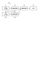
図1は、第1の実施形態に係るイメージセンサを搭載した電子機器の概略構成例を示すブロック図である。図1に示すように、電子機器1は、例えば、撮像レンズ2と、イメージセンサ100と、記憶部3と、プロセッサ4とを備える。 1.1 Configuration Example of Electronic Device FIG. 1 is a block diagram showing a schematic configuration example of an electronic device equipped with an image sensor according to the first embodiment. As shown in FIG. 1, theelectronic device 1 includes, for example, an image pickup lens 2, an image sensor 100, a storage unit 3, and a processor 4.
図1は、第1の実施形態に係るイメージセンサを搭載した電子機器の概略構成例を示すブロック図である。図1に示すように、電子機器1は、例えば、撮像レンズ2と、イメージセンサ100と、記憶部3と、プロセッサ4とを備える。 1.1 Configuration Example of Electronic Device FIG. 1 is a block diagram showing a schematic configuration example of an electronic device equipped with an image sensor according to the first embodiment. As shown in FIG. 1, the
撮像レンズ2は、入射光を集光してその像をイメージセンサ100の受光面に結像する光学系の一例である。受光面とは、イメージセンサ100における光電変換部が配列する面であってよい。イメージセンサ100は、入射光を光電変換して画像データを生成する。また、イメージセンサ100は、生成した画像データに対し、ノイズ除去やホワイトバランス調整等の所定の信号処理を実行する。
The image pickup lens 2 is an example of an optical system that collects incident light and forms an image on the light receiving surface of the image sensor 100. The light receiving surface may be a surface on which the photoelectric conversion units of the image sensor 100 are arranged. The image sensor 100 photoelectrically converts the incident light to generate image data. Further, the image sensor 100 executes predetermined signal processing such as noise reduction and white balance adjustment on the generated image data.
記憶部3は、例えば、フラッシュメモリやDRAM(Dynamic Random Access Memory)やSRAM(Static Random Access Memory)等で構成され、イメージセンサ100から入力された画像データ等を記録する。
The storage unit 3 is composed of, for example, a flash memory, a DRAM (Dynamic Random Access Memory), a SRAM (Static Random Access Memory), or the like, and records image data or the like input from the image sensor 100.
プロセッサ4は、例えば、CPU(Central Processing Unit)等を用いて構成され、オペレーティングシステムや各種アプリケーションソフトウエア等を実行するアプリケーションプロセッサや、GPU(Graphics Processing Unit)やベースバンドプロセッサなどが含まれ得る。プロセッサ4は、イメージセンサ100から入力された画像データや記憶部3から読み出した画像データ等に対し、必要に応じた種々処理を実行したり、ユーザへの表示を実行したり、所定のネットワークを介して外部へ送信したりする。
The processor 4 is configured by using, for example, a CPU (Central Processing Unit) or the like, and may include an application processor that executes an operating system, various application software, and the like, a GPU (Graphics Processing Unit), a baseband processor, and the like. The processor 4 executes various processes as necessary for the image data input from the image sensor 100, the image data read from the storage unit 3, and the like, displays the image to the user, and establishes a predetermined network. Send to the outside via.
また、プロセッサ4は、後述するRGB画素10から読み出されたカラー画像と、IR画素20から読み出されたモノクロ画像(IR画像)とを統合的に処理することで、測距処理や認識処理などの種々の処理を実行し得る。
Further, the processor 4 integrates the color image read from the RGB pixel 10 described later and the monochrome image (IR image) read from the IR pixel 20 to perform distance measurement processing and recognition processing. Various processes such as can be executed.
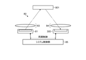
1.2 認識システムの機能構成例
次に、電子機器1を用いて構成される認識システムの機能構成例について説明する。図2は、第1の実施形態に係る認識システムの機能構成例を示すブロック図である。図2に示すように、認識システム70は、RGBセンサ部71とIRセンサ部73との2種類のセンサ部を備える。また、認識システム70は、RGB画像処理部72と、IR画像処理部74と、認識処理部75と、インタフェース(I/F)部76とを備える。 1.2 Example of functional configuration of the recognition system Next, an example of the functional configuration of the recognition system configured by using theelectronic device 1 will be described. FIG. 2 is a block diagram showing a functional configuration example of the recognition system according to the first embodiment. As shown in FIG. 2, the recognition system 70 includes two types of sensor units, an RGB sensor unit 71 and an IR sensor unit 73. Further, the recognition system 70 includes an RGB image processing unit 72, an IR image processing unit 74, a recognition processing unit 75, and an interface (I / F) unit 76.
次に、電子機器1を用いて構成される認識システムの機能構成例について説明する。図2は、第1の実施形態に係る認識システムの機能構成例を示すブロック図である。図2に示すように、認識システム70は、RGBセンサ部71とIRセンサ部73との2種類のセンサ部を備える。また、認識システム70は、RGB画像処理部72と、IR画像処理部74と、認識処理部75と、インタフェース(I/F)部76とを備える。 1.2 Example of functional configuration of the recognition system Next, an example of the functional configuration of the recognition system configured by using the
RGBセンサ部71は、例えば、RGB三原色それぞれの波長成分を透過するカラーフィルタを備える複数の画素(以下、RGB画素という)を備え、RGB三原色の色成分で構成されたカラー画像(以下、RGB画像という)を生成する。なお、RGBセンサ部71に代えて、CMY三原色それぞれの波長成分を透過するカラーフィルタを備える複数の画素を備えるセンサ部等が用いられてもよい。
The RGB sensor unit 71 includes, for example, a plurality of pixels (hereinafter referred to as RGB pixels) having a color filter that transmits the wavelength components of each of the three primary colors of RGB, and is a color image composed of the color components of the three primary colors of RGB (hereinafter referred to as an RGB image). ) Is generated. Instead of the RGB sensor unit 71, a sensor unit or the like having a plurality of pixels including a color filter that transmits wavelength components of each of the three primary colors of CMY may be used.
IRセンサ部73は、例えば、赤外(IR)光を透過するIRフィルタを備える複数の画素(以下、IR画素という)を備え、IR光の色成分で構成されたモノクロ画像(以下、IR画像という)を生成する。なお、IRセンサ部73に代えて、他の1以上の波長帯の光をそれぞれ透過するカラーフィルタを備える複数の画素を備えるセンサ部等が用いられてもよい。
The IR sensor unit 73 includes, for example, a plurality of pixels (hereinafter referred to as IR pixels) including an IR filter that transmits infrared (IR) light, and is a monochrome image composed of color components of IR light (hereinafter referred to as IR image). ) Is generated. Instead of the IR sensor unit 73, a sensor unit or the like having a plurality of pixels including a color filter that transmits light in another wavelength band of one or more may be used.
RGB画像処理部72は、RGBセンサ部71から入力されたRGB画像データに対し、ノイズ除去やホワイトバランス調整や画素補間等の所定の信号処理を実行する。
The RGB image processing unit 72 executes predetermined signal processing such as noise removal, white balance adjustment, and pixel interpolation for the RGB image data input from the RGB sensor unit 71.
IR画像処理部74は、IRセンサ部73から入力されたIR画像データに対し、ノイズ除去やホワイトバランス調整等の所定の信号処理を実行する。
The IR image processing unit 74 executes predetermined signal processing such as noise removal and white balance adjustment on the IR image data input from the IR sensor unit 73.
認識処理部75は、RGB画像処理部72から入力されたRGB画像データ及び/又はIR画像処理部74から入力されたIR画像データを用いて、RGBセンサ部71及び/又はIRセンサ部73の画角内に存在する物体等の認識処理を実行する。認識処理部75による認識処理には、パターン認識などの認識処理や、人工知能(Artificial Intelligence:AI)による認識処理などが用いられてよい。AIによる認識処理には、例えば、CNN(Convolution Neural Network)やRNN(Recurrent Neural Network)などのニューラルネットワークを利用した深層学習が適用されてもよい。また、認識処理部75は、認識処理の一部を実行し、その結果(中間データ等)を出力してもよい。
The recognition processing unit 75 uses the RGB image data input from the RGB image processing unit 72 and / or the IR image data input from the IR image processing unit 74 to image the image of the RGB sensor unit 71 and / or the IR sensor unit 73. Executes recognition processing for objects existing in the corner. For the recognition process by the recognition processing unit 75, a recognition process such as pattern recognition, a recognition process by artificial intelligence (AI), or the like may be used. For example, deep learning using a neural network such as CNN (Convolution Neural Network) or RNN (Recurrent Neural Network) may be applied to the recognition process by AI. Further, the recognition processing unit 75 may execute a part of the recognition processing and output the result (intermediate data or the like).
インタフェース部76は、認識処理部75により得られた認識結果(中間データ等を含む)や、RGBセンサ部71及び/又はIRセンサ部73で取得された画像データを外部の例えばプロセッサ4及び/又は記憶部3へ出力する。
The interface unit 76 uses the recognition result (including intermediate data and the like) obtained by the recognition processing unit 75 and the image data acquired by the RGB sensor unit 71 and / or the IR sensor unit 73 as an external example, the processor 4 and / or. Output to the storage unit 3.
なお、RGB画像処理部72は、RGB画像データに対して物体の領域判定を実行し、その結果として得られた注目領域(Region of Interest:ROI)を指定するアドレス等の情報(以下、単にROI情報と言いう)をIRセンサ部73及び/又はIR画像処理部74に入力してもよい。これに対し、IRセンサ部73は、RGB画像処理部72から入力されたROI情報に対応する領域のIR画像データを取得するように動作してもよい。若しくは、IR画像処理部74は、IRセンサ部73から入力されたIR画像データに対し、RGB画像処理部72から入力されたROI情報に対応する領域のトリミングなどの処理を実行してもよい。
The RGB image processing unit 72 executes the area determination of the object with respect to the RGB image data, and the information such as the address for designating the region of interest (Region of Interest: ROI) obtained as a result (hereinafter, simply ROI). Information) may be input to the IR sensor unit 73 and / or the IR image processing unit 74. On the other hand, the IR sensor unit 73 may operate so as to acquire IR image data in a region corresponding to the ROI information input from the RGB image processing unit 72. Alternatively, the IR image processing unit 74 may execute processing such as trimming of a region corresponding to the ROI information input from the RGB image processing unit 72 on the IR image data input from the IR sensor unit 73.
1.3 イメージセンサの構成例
図3は、第1の実施形態に係るイメージセンサの概略構成例を示すブロック図である。図3に示すように、本実施形態に係るイメージセンサ100は、例えば、画素アレイ部101と、RGB画素駆動回路102Aと、IR画素駆動回路102Bと、RGB信号処理回路103Aと、IR信号処理回路103Bと、カラム駆動回路104と、システム制御回路105と、RGBデータ処理部108Aと、IRデータ処理部108Bとを備える。 1.3 Configuration example of the image sensor FIG. 3 is a block diagram showing a schematic configuration example of the image sensor according to the first embodiment. As shown in FIG. 3, theimage sensor 100 according to the present embodiment includes, for example, a pixel array unit 101, an RGB pixel drive circuit 102A, an IR pixel drive circuit 102B, an RGB signal processing circuit 103A, and an IR signal processing circuit. It includes 103B, a column drive circuit 104, a system control circuit 105, an RGB data processing unit 108A, and an IR data processing unit 108B.
図3は、第1の実施形態に係るイメージセンサの概略構成例を示すブロック図である。図3に示すように、本実施形態に係るイメージセンサ100は、例えば、画素アレイ部101と、RGB画素駆動回路102Aと、IR画素駆動回路102Bと、RGB信号処理回路103Aと、IR信号処理回路103Bと、カラム駆動回路104と、システム制御回路105と、RGBデータ処理部108Aと、IRデータ処理部108Bとを備える。 1.3 Configuration example of the image sensor FIG. 3 is a block diagram showing a schematic configuration example of the image sensor according to the first embodiment. As shown in FIG. 3, the
画素アレイ部101、RGB画素駆動回路102A、RGB信号処理回路103A、カラム駆動回路104及びシステム制御回路105は、例えば、図2におけるRGBセンサ部71を構成し、画素アレイ部101、IR画素駆動回路102B、IR信号処理回路103B、カラム駆動回路104及びシステム制御回路105は、例えば、図2におけるIRセンサ部73を構成する。また、RGB信号処理回路103A及びRGBデータ処理部108Aは、例えば、図2におけるRGB画像処理部72を構成し、IR信号処理回路103B及びIRデータ処理部108Bは、例えば、図2におけるIR画像処理部74を構成する。なお、図2における認識処理部75は、プロセッサ4単体で実現されてもよいし、RGBデータ処理部108A及びIRデータ処理部108Bとプロセッサ4とを連携させることで実現されてもよいし、RGBデータ処理部108AとIRデータ処理部108Bとを連携させることで実現されてもよい。
The pixel array unit 101, the RGB pixel drive circuit 102A, the RGB signal processing circuit 103A, the column drive circuit 104, and the system control circuit 105 form, for example, the RGB sensor unit 71 in FIG. 2, the pixel array unit 101, and the IR pixel drive circuit. The 102B, the IR signal processing circuit 103B, the column drive circuit 104, and the system control circuit 105 form, for example, the IR sensor unit 73 in FIG. 2. Further, the RGB signal processing circuit 103A and the RGB data processing unit 108A constitute, for example, the RGB image processing unit 72 in FIG. 2, and the IR signal processing circuit 103B and the IR data processing unit 108B form, for example, the IR image processing in FIG. 2. It constitutes a part 74. The recognition processing unit 75 in FIG. 2 may be realized by the processor 4 alone, may be realized by linking the RGB data processing unit 108A and the IR data processing unit 108B with the processor 4, or RGB. It may be realized by linking the data processing unit 108A and the IR data processing unit 108B.
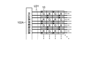
画素アレイ部101は、単位画素110が行方向及び列方向に、すなわち、2次元格子状(行列状ともいう)に配置された構成を有する。ここで、行方向とは画素行の画素の配列方向(図面中、横方向)をいい、列方向とは画素列の画素の配列方向(図面中、縦方向)をいう。
The pixel array unit 101 has a configuration in which unit pixels 110 are arranged in a row direction and a column direction, that is, in a two-dimensional grid pattern (also referred to as a matrix pattern). Here, the row direction means the arrangement direction of the pixels in the pixel row (in the drawing, the horizontal direction), and the column direction means the arrangement direction of the pixels in the pixel row (in the drawing, the vertical direction).
各単位画素110は、RGB画素10とIR画素20とを備える。以下の説明において、RGB画素10とIR画素20とを区別しない場合、単に画素と称する場合がある。単位画素110の具体的な回路構成や画素構造の詳細については後述するが、RGB画素10及びIR画素20それぞれは、受光した光量に応じた電荷を生成しかつ蓄積する光電変換部を備え、入射光量に応じた電圧の画素信号を生成する。
Each unit pixel 110 includes an RGB pixel 10 and an IR pixel 20. In the following description, when the RGB pixel 10 and the IR pixel 20 are not distinguished, they may be simply referred to as pixels. The specific circuit configuration and pixel structure of the unit pixel 110 will be described later, but each of the RGB pixels 10 and the IR pixels 20 is provided with a photoelectric conversion unit that generates and stores charges according to the amount of received light, and is incident. A pixel signal with a voltage corresponding to the amount of light is generated.
画素アレイ部101では、行列状の画素配列に対し、画素行ごとに画素駆動線LD1及びLD2が行方向に沿って配線され、画素列ごとに垂直信号線VSL1及びVSL2が列方向に沿って配線されている。例えば、画素駆動線LD1は、各行のRGB画素10に接続され、画素駆動線LD2は、各行のIR画素20に接続される。一方、例えば、垂直信号線VSL1は、各列のRGB画素10に接続され、垂直信号線VSL2は、各列のIR画素20に接続される。ただし、これに限定されず、画素駆動線LD1及びLD2は、互いに直交するように配線されていてもよい。同様に、垂直信号線VSL1及びVSL2は、互いに直交するように配線されていてもよい。例えば、画素駆動線LD1が行方向に配線され、画素駆動線LD2が列方向に配線され、垂直信号線VSL1が列方向に配線され、垂直信号線VSL2が行方向に配線されてもよい。
In the pixel array unit 101, the pixel drive lines LD1 and LD2 are wired along the row direction for each pixel row with respect to the matrix-shaped pixel array, and the vertical signal lines VSL1 and VSL2 are wired along the column direction for each pixel row. Has been done. For example, the pixel drive line LD1 is connected to the RGB pixel 10 of each line, and the pixel drive line LD2 is connected to the IR pixel 20 of each line. On the other hand, for example, the vertical signal line VSL1 is connected to the RGB pixels 10 in each row, and the vertical signal line VSL2 is connected to the IR pixels 20 in each row. However, the present invention is not limited to this, and the pixel drive lines LD1 and LD2 may be wired so as to be orthogonal to each other. Similarly, the vertical signal lines VSL1 and VSL2 may be wired so as to be orthogonal to each other. For example, the pixel drive line LD1 may be wired in the row direction, the pixel drive line LD2 may be wired in the column direction, the vertical signal line VSL1 may be wired in the column direction, and the vertical signal line VSL2 may be wired in the row direction.
画素駆動線LD1は、RGB画素10から画素信号を読み出す際の駆動を行うための制御信号を伝送する。画素駆動線LD2は、IR画素20から画素信号を読み出す際の駆動を行うための制御信号を伝送する。図3では、画素駆動線LD1及びLD2がそれぞれ1本ずつの配線として示されているが、1本ずつに限られるものではない。画素駆動線LD1の一端は、RGB画素駆動回路102Aの各行に対応した出力端に接続され、画素駆動線LD2の一端は、IR画素駆動回路102Bの各行に対応した出力端に接続される。
The pixel drive line LD1 transmits a control signal for driving when reading a pixel signal from the RGB pixel 10. The pixel drive line LD2 transmits a control signal for driving when reading a pixel signal from the IR pixel 20. In FIG. 3, the pixel drive lines LD1 and LD2 are shown as one wiring each, but the wiring is not limited to one. One end of the pixel drive line LD1 is connected to the output end corresponding to each line of the RGB pixel drive circuit 102A, and one end of the pixel drive line LD2 is connected to the output end corresponding to each line of the IR pixel drive circuit 102B.
RGB画素駆動回路102A及びIR画素駆動回路102Bそれぞれは、シフトレジスタやアドレスデコーダなどによって構成され、画素アレイ部101の各画素を全画素同時あるいは行単位等で駆動する。すなわち、RGB画素駆動回路102Aは、当該RGB画素駆動回路102Aを制御するシステム制御回路105と共に、画素アレイ部101の各RGB画素10の動作を制御する駆動部を構成し、IR画素駆動回路102Bは、当該IR画素駆動回路102Bを制御するシステム制御回路105と共に、画素アレイ部101の各IR画素20の動作を制御する駆動部を構成する。これらRGB画素駆動回路102A及びIR画素駆動回路102Bは、その具体的な構成については図示を省略するが、一般的に、読出し走査系と掃出し走査系との2つの走査系を備えている。
Each of the RGB pixel drive circuit 102A and the IR pixel drive circuit 102B is configured by a shift register, an address decoder, or the like, and drives each pixel of the pixel array unit 101 simultaneously or row by row. That is, the RGB pixel drive circuit 102A constitutes a drive unit that controls the operation of each RGB pixel 10 of the pixel array unit 101 together with the system control circuit 105 that controls the RGB pixel drive circuit 102A, and the IR pixel drive circuit 102B Along with the system control circuit 105 that controls the IR pixel drive circuit 102B, a drive unit that controls the operation of each IR pixel 20 of the pixel array unit 101 is configured. The RGB pixel drive circuit 102A and the IR pixel drive circuit 102B are generally provided with two scanning systems, a read scanning system and a sweep scanning system, although the specific configuration thereof is not shown.
読出し走査系は、各画素から信号を読み出すために、画素アレイ部101の各画素を行単位で順に選択走査する。各画素から読み出される画素信号はアナログ信号である。掃出し走査系は、読出し走査系によって読出し走査が行われる読出し行に対して、その読出し走査よりも露光時間分だけ先行して掃出し走査を行う。
The read scanning system selectively scans each pixel of the pixel array unit 101 row by row in order to read a signal from each pixel. The pixel signal read from each pixel is an analog signal. The sweep scan system performs sweep scan for the read row on which read scan is performed by the read scan system, ahead of the read scan by the exposure time.
この掃出し走査系による掃出し走査により、読出し行の各画素の光電変換部から不要な電荷が掃き出されることによって当該光電変換部がリセットされる。そして、この掃出し走査系で不要電荷を掃き出す(リセットする)ことにより、所謂電子シャッタ動作が行われる。ここで、電子シャッタ動作とは、光電変換部の電荷を捨てて、新たに露光を開始する(電荷の蓄積を開始する)動作のことを言う。
By the sweep scan by this sweep scan system, the photoelectric conversion unit is reset by sweeping out unnecessary charges from the photoelectric conversion unit of each pixel in the read row. Then, by sweeping out (resetting) unnecessary charges with this sweeping scanning system, a so-called electronic shutter operation is performed. Here, the electronic shutter operation refers to an operation in which the electric charge of the photoelectric conversion unit is discarded and a new exposure is started (charge accumulation is started).
読出し走査系による読出し動作によって読み出される信号は、その直前の読出し動作または電子シャッタ動作以降に受光した光量に対応している。そして、直前の読出し動作による読出しタイミングまたは電子シャッタ動作による掃出しタイミングから、今回の読出し動作による読出しタイミングまでの期間が、各画素における電荷の蓄積期間(露光期間ともいう)となる。
The signal read by the read operation by the read scanning system corresponds to the amount of light received after the read operation or the electronic shutter operation immediately before that. The period from the read timing by the immediately preceding read operation or the sweep timing by the electronic shutter operation to the read timing by the current read operation is the charge accumulation period (also referred to as an exposure period) in each pixel.
RGB画素駆動回路102Aによって選択走査された画素行の各RGB画素10から出力される画素信号は、画素列ごとに垂直信号線VSL1の各々を通してRGB信号処理回路103Aに入力される。RGB信号処理回路103Aは、画素アレイ部101の画素列ごとに、選択行の各RGB画素10から垂直信号線VSL1を通して出力される画素信号に対して所定の信号処理を行うとともに、信号処理後の画素信号を一時的に保持する。
The pixel signal output from each of the RGB pixels 10 in the pixel row selected and scanned by the RGB pixel drive circuit 102A is input to the RGB signal processing circuit 103A through each of the vertical signal lines VSL1 for each pixel column. The RGB signal processing circuit 103A performs predetermined signal processing on the pixel signal output from each RGB pixel 10 in the selected row through the vertical signal line VSL1 for each pixel row of the pixel array unit 101, and after the signal processing, the pixel signal is processed. Temporarily holds the pixel signal.
同様に、IR画素駆動回路102Bによって選択走査された画素行の各IR画素20から出力される画素信号は、画素列ごとに垂直信号線VSL2の各々を通してIR信号処理回路103Bに入力される。IR信号処理回路103Bは、画素アレイ部101の画素列ごとに、選択行の各IR画素20から垂直信号線VSL2を通して出力される画素信号に対して所定の信号処理を行うとともに、信号処理後の画素信号を一時的に保持する。
Similarly, the pixel signal output from each IR pixel 20 in the pixel row selectively scanned by the IR pixel drive circuit 102B is input to the IR signal processing circuit 103B through each of the vertical signal lines VSL2 for each pixel column. The IR signal processing circuit 103B performs predetermined signal processing on the pixel signal output from each IR pixel 20 in the selected row through the vertical signal line VSL2 for each pixel row of the pixel array unit 101, and after the signal processing, the IR signal processing circuit 103B performs predetermined signal processing. Temporarily hold the pixel signal.
具体的には、RGB信号処理回路103A及びIR信号処理回路103Bそれぞれは、信号処理として少なくとも、ノイズ除去処理、例えばCDS(Correlated Double Sampling:相関二重サンプリング)処理や、DDS(Double Data Sampling)処理を行う。例えば、CDS処理により、リセットノイズや画素内の増幅トランジスタの閾値ばらつき等の画素固有の固定パターンノイズが除去される。RGB信号処理回路103A及びIR信号処理回路103Bそれぞれは、その他にも、例えば、AD(アナログ-デジタル)変換機能を備え、光電変換部から読み出されたアナログの画素信号をデジタル信号に変換して出力する。
Specifically, each of the RGB signal processing circuit 103A and the IR signal processing circuit 103B has at least noise reduction processing, for example, CDS (Correlated Double Sampling) processing and DDS (Double Data Sampling) processing as signal processing. I do. For example, the CDS process removes pixel-specific fixed pattern noise such as reset noise and threshold variation of the amplification transistor in the pixel. Each of the RGB signal processing circuit 103A and the IR signal processing circuit 103B also has, for example, an AD (analog-digital) conversion function, and converts an analog pixel signal read from a photoelectric conversion unit into a digital signal. Output.
カラム駆動回路104は、シフトレジスタやアドレスデコーダなどによって構成され、RGB信号処理回路103A及びIR信号処理回路103Bの画素列に対応する読出し回路(以下、画素回路という)を順番に選択する。このカラム駆動回路104による選択走査により、RGB信号処理回路103A及びIR信号処理回路103Bにおいて画素回路ごとに信号処理された画素信号が順番に出力される。
The column drive circuit 104 is composed of a shift register, an address decoder, and the like, and sequentially selects a read circuit (hereinafter referred to as a pixel circuit) corresponding to the pixel strings of the RGB signal processing circuit 103A and the IR signal processing circuit 103B. By the selective scanning by the column drive circuit 104, the pixel signals processed by the RGB signal processing circuit 103A and the IR signal processing circuit 103B are sequentially output for each pixel circuit.
システム制御回路105は、各種のタイミング信号を生成するタイミングジェネレータなどによって構成され、当該タイミングジェネレータで生成された各種のタイミングを基に、RGB画素駆動回路102A、IR画素駆動回路102B、RGB信号処理回路103A、IR信号処理回路103B、及び、カラム駆動回路104などの駆動制御を行う。
The system control circuit 105 is configured by a timing generator or the like that generates various timing signals, and based on the various timings generated by the timing generator, the RGB pixel drive circuit 102A, the IR pixel drive circuit 102B, and the RGB signal processing circuit Drive control is performed on the 103A, the IR signal processing circuit 103B, the column drive circuit 104, and the like.
RGBデータ処理部108A及びIRデータ処理部108Bそれぞれは、少なくとも演算処理機能を有し、RGB信号処理回路103A又はIR信号処理回路103Bから出力される画像信号に対して演算処理等の種々の信号処理を行う。
Each of the RGB data processing unit 108A and the IR data processing unit 108B has at least an arithmetic processing function, and various signal processing such as arithmetic processing for the image signal output from the RGB signal processing circuit 103A or the IR signal processing circuit 103B. I do.
RGBデータ処理部108A又はIRデータ処理部108Bから出力された画像データは、例えば、イメージセンサ100を搭載する電子機器1におけるプロセッサ4等において所定の処理が実行されたり、所定のネットワークを介して外部へ送信されたりしてもよい。
The image data output from the RGB data processing unit 108A or the IR data processing unit 108B is, for example, executed by a processor 4 or the like in the electronic device 1 equipped with the image sensor 100, or is external via a predetermined network. It may be sent to.
なお、イメージセンサ100は、RGBデータ処理部108A及びIRデータ処理部108Bでの信号処理に必要なデータや、RGB信号処理回路103A、IR信号処理回路103B、RGBデータ処理部108A及びIRデータ処理部108Bのうちのいずれか1つ以上で処理されたデータ等を一時的に保持するための記憶部を備えていてもよい。
The image sensor 100 includes data required for signal processing in the RGB data processing unit 108A and the IR data processing unit 108B, the RGB signal processing circuit 103A, the IR signal processing circuit 103B, the RGB data processing unit 108A, and the IR data processing unit. A storage unit for temporarily holding data or the like processed by any one or more of 108B may be provided.
1.3.1 イメージセンサの変形例
図4は、第1の実施形態の変形例に係るイメージセンサの概略構成例を示すブロック図である。上述した図3では、RGB画素10及びIR画素20それぞれに対して別々の信号処理回路(RGB信号処理回路103A及びIR信号処理回路103B)を設けた場合を例示したが、これに限定されず、図4に例示するように、RGB画素10及びIR画素20に対して共通の信号処理回路103を設けることも可能である。その場合、RGB画素10からの画素信号の読出しと、IR画素20からの画素信号の読出しとは、時分割で実行されてもよいし、並行して実行されてもよい。 1.3.1 Modification example of image sensor FIG. 4 is a block diagram showing a schematic configuration example of an image sensor according to a modification of the first embodiment. In FIG. 3 described above, a case where separate signal processing circuits (RGBsignal processing circuit 103A and IR signal processing circuit 103B) are provided for each of the RGB pixel 10 and the IR pixel 20 is illustrated, but the present invention is not limited to this. As illustrated in FIG. 4, it is also possible to provide a common signal processing circuit 103 for the RGB pixels 10 and the IR pixels 20. In that case, the reading of the pixel signal from the RGB pixel 10 and the reading of the pixel signal from the IR pixel 20 may be executed in a time division manner or may be executed in parallel.
図4は、第1の実施形態の変形例に係るイメージセンサの概略構成例を示すブロック図である。上述した図3では、RGB画素10及びIR画素20それぞれに対して別々の信号処理回路(RGB信号処理回路103A及びIR信号処理回路103B)を設けた場合を例示したが、これに限定されず、図4に例示するように、RGB画素10及びIR画素20に対して共通の信号処理回路103を設けることも可能である。その場合、RGB画素10からの画素信号の読出しと、IR画素20からの画素信号の読出しとは、時分割で実行されてもよいし、並行して実行されてもよい。 1.3.1 Modification example of image sensor FIG. 4 is a block diagram showing a schematic configuration example of an image sensor according to a modification of the first embodiment. In FIG. 3 described above, a case where separate signal processing circuits (RGB
1.4 単位画素の構成例
次に、単位画素110の構成例について説明する。なお、ここでは、単位画素110が、RGB三原色のRGB画像を取得するためのRGB画素10と、赤外(IR)光のIR画像を取得するためのIR画素20とを含む場合を例示に挙げる。なお、図5及び以下では、RGB三原色を構成する各色成分の光を透過させるカラーフィルタ31r、31g又は31bを区別しない場合、その符号が31とされている。 1.4 Configuration example of unit pixel Next, a configuration example ofunit pixel 110 will be described. Here, a case where the unit pixel 110 includes an RGB pixel 10 for acquiring an RGB image of the three primary colors of RGB and an IR pixel 20 for acquiring an IR image of infrared (IR) light will be given as an example. .. In FIG. 5 and the following, when the color filters 31r, 31g, or 31b that transmit the light of each color component constituting the three primary colors of RGB are not distinguished, the reference numeral is 31.
次に、単位画素110の構成例について説明する。なお、ここでは、単位画素110が、RGB三原色のRGB画像を取得するためのRGB画素10と、赤外(IR)光のIR画像を取得するためのIR画素20とを含む場合を例示に挙げる。なお、図5及び以下では、RGB三原色を構成する各色成分の光を透過させるカラーフィルタ31r、31g又は31bを区別しない場合、その符号が31とされている。 1.4 Configuration example of unit pixel Next, a configuration example of
図5は、第1の実施形態に係る画素アレイ部の概略構成例を示す模式図である。図5に示すように、画素アレイ部101は、RGB画素10とIR画素20とからなる単位画素110が光の入射方向に沿って配列した構造を備える単位画素110が2次元格子状に配列した構成を備える。すなわち、本実施形態では、RGB画素10とIR画素20とが単位画素110の配列方向(平面方向)に対して垂直方向に位置されており、入射光の光路における上流側に位置するRGB画素10を透過した光が、このRGB画素10の下流側に位置するIR画素20に入射するように構成されている。このような構成によれば、RGB画素10の光電変換部PD1における入射光の入射面と反対側の面側にIR画素20の光電変換部PD2が配置される。それにより、本実施形態では、光の入射方向に沿って配列するRGB画素10とIR画素20との入射光の光軸が一致又は略一致している。
FIG. 5 is a schematic diagram showing a schematic configuration example of the pixel array unit according to the first embodiment. As shown in FIG. 5, in the pixel array unit 101, unit pixels 110 having a structure in which unit pixels 110 composed of RGB pixels 10 and IR pixels 20 are arranged along the incident direction of light are arranged in a two-dimensional grid pattern. It has a configuration. That is, in the present embodiment, the RGB pixels 10 and the IR pixels 20 are located in the direction perpendicular to the arrangement direction (planar direction) of the unit pixels 110, and the RGB pixels 10 are located on the upstream side in the optical path of the incident light. The light transmitted through the image is configured to enter the IR pixel 20 located on the downstream side of the RGB pixel 10. According to such a configuration, the photoelectric conversion unit PD2 of the IR pixel 20 is arranged on the surface side opposite to the incident surface of the incident light in the photoelectric conversion unit PD1 of the RGB pixel 10. As a result, in the present embodiment, the optical axes of the incident light of the RGB pixels 10 and the IR pixels 20 arranged along the incident direction of the light are coincident or substantially the same.
なお、本実施形態では、RGB画素10を構成する光電変換部PD1を有機材料で構成し、IR画素20を構成する光電変換部PD2をシリコンなどの半導体材料で構成する場合を例示するが、これに限定されるものではない。例えば、光電変換部PD1と光電変換部PD2との両方が半導体材料で構成されてもよいし、光電変換部PD1と光電変換部PD2との両方が有機材料で構成されてもよいし、光電変換部PD1が半導体材料で構成され、光電変換部PD2が有機材料で構成されてもよい。若しくは、光電変換部PD1と光電変換部PD2との少なくとも一方が有機材料及び半導体材料とは異なる光電変換材料で構成されてもよい。
In this embodiment, the case where the photoelectric conversion unit PD1 constituting the RGB pixel 10 is composed of an organic material and the photoelectric conversion unit PD2 constituting the IR pixel 20 is composed of a semiconductor material such as silicon will be exemplified. Not limited to. For example, both the photoelectric conversion unit PD1 and the photoelectric conversion unit PD2 may be made of a semiconductor material, or both the photoelectric conversion unit PD1 and the photoelectric conversion unit PD2 may be made of an organic material, or the photoelectric conversion unit may be made of an organic material. The part PD1 may be made of a semiconductor material, and the photoelectric conversion part PD2 may be made of an organic material. Alternatively, at least one of the photoelectric conversion unit PD1 and the photoelectric conversion unit PD2 may be made of a photoelectric conversion material different from the organic material and the semiconductor material.
1.5 単位画素の回路構成例
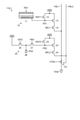
次に、単位画素110の回路構成例について説明する。図6は、第1実施形態に係る単位画素の概略構成例を示す回路図である。図6に示すように、単位画素110は、RGB画素10と、IR画素20とを1つずつ備える。 1.5 Example of circuit configuration of unit pixel Next, an example of circuit configuration ofunit pixel 110 will be described. FIG. 6 is a circuit diagram showing a schematic configuration example of a unit pixel according to the first embodiment. As shown in FIG. 6, the unit pixel 110 includes one RGB pixel 10 and one IR pixel 20.
次に、単位画素110の回路構成例について説明する。図6は、第1実施形態に係る単位画素の概略構成例を示す回路図である。図6に示すように、単位画素110は、RGB画素10と、IR画素20とを1つずつ備える。 1.5 Example of circuit configuration of unit pixel Next, an example of circuit configuration of
(RGB画素10)
RGB画素10は、例えば、光電変換部PD1と、転送ゲート11と、浮遊拡散領域FD1と、リセットトランジスタ12と、増幅トランジスタ13と、選択トランジスタ14とを備える。 (RGB pixel 10)
TheRGB pixel 10 includes, for example, a photoelectric conversion unit PD1, a transfer gate 11, a floating diffusion region FD1, a reset transistor 12, an amplification transistor 13, and a selection transistor 14.
RGB画素10は、例えば、光電変換部PD1と、転送ゲート11と、浮遊拡散領域FD1と、リセットトランジスタ12と、増幅トランジスタ13と、選択トランジスタ14とを備える。 (RGB pixel 10)
The
選択トランジスタ14のゲートには、画素駆動線LD1に含まれる選択制御線が接続され、リセットトランジスタ12のゲートには、画素駆動線LD1に含まれるリセット制御線が接続され、転送ゲート11の後述する蓄積電極(後述において説明する図10の蓄積電極37参照)には、画素駆動線LD1に含まれる転送制御線が接続される。また、増幅トランジスタ13のドレインには、RGB信号処理回路103Aに一端が接続される垂直信号線VSL1が選択トランジスタ14を介して接続される。
The selection control line included in the pixel drive line LD1 is connected to the gate of the selection transistor 14, and the reset control line included in the pixel drive line LD1 is connected to the gate of the reset transistor 12, which will be described later. A transfer control line included in the pixel drive line LD1 is connected to the storage electrode (see the storage electrode 37 in FIG. 10 described later). Further, a vertical signal line VSL1 having one end connected to the RGB signal processing circuit 103A is connected to the drain of the amplification transistor 13 via the selection transistor 14.
以下の説明において、リセットトランジスタ12、増幅トランジスタ13及び選択トランジスタ14は、まとめて画素回路とも称される。この画素回路には、浮遊拡散領域FD1及び/又は転送ゲート11が含まれてもよい。
In the following description, the reset transistor 12, the amplification transistor 13, and the selection transistor 14 are collectively referred to as a pixel circuit. The pixel circuit may include a stray diffusion region FD1 and / or a transfer gate 11.
光電変換部PD1は、例えば有機材料で構成され、入射した光を光電変換する。転送ゲート11は、光電変換部PD1に発生した電荷を転送する。浮遊拡散領域FD1は、転送ゲート11が転送した電荷を蓄積する。増幅トランジスタ13は、浮遊拡散領域FD1に蓄積された電荷に応じた電圧値の画素信号を垂直信号線VSL1に出現させる。リセットトランジスタ12は、浮遊拡散領域FD1に蓄積された電荷を放出する。選択トランジスタ14は、読出し対象のRGB画素10を選択する。
The photoelectric conversion unit PD1 is made of, for example, an organic material, and performs photoelectric conversion of incident light. The transfer gate 11 transfers the electric charge generated in the photoelectric conversion unit PD1. The floating diffusion region FD1 accumulates the electric charge transferred by the transfer gate 11. The amplification transistor 13 causes a pixel signal having a voltage value corresponding to the electric charge stored in the stray diffusion region FD1 to appear on the vertical signal line VSL1. The reset transistor 12 emits the electric charge accumulated in the stray diffusion region FD1. The selection transistor 14 selects the RGB pixel 10 to be read.
光電変換部PD1のアノードは、接地されており、カソ-ドは、転送ゲート11に接続される。転送ゲート11は、その詳細については後述において図10を用いて説明するが、例えば、蓄積電極37と読出し電極36とを備える。露光時には、光電変換部PD1に発生した電荷を蓄積電極37の近傍の半導体層35に集めるための電圧が、転送制御線を介して蓄積電極37に印加される。読出し時には、蓄積電極37の近傍の半導体層35に集められた電荷を読出し電極36を介して流出させるための電圧が、転送制御線を介して蓄積電極37に印加される。
The anode of the photoelectric conversion unit PD1 is grounded, and the cascade is connected to the transfer gate 11. The details of the transfer gate 11 will be described later with reference to FIG. 10, but the transfer gate 11 includes, for example, a storage electrode 37 and a read electrode 36. At the time of exposure, a voltage for collecting the electric charge generated in the photoelectric conversion unit PD1 in the semiconductor layer 35 in the vicinity of the storage electrode 37 is applied to the storage electrode 37 via the transfer control line. At the time of reading, a voltage for causing the electric charge collected in the semiconductor layer 35 in the vicinity of the storage electrode 37 to flow out through the reading electrode 36 is applied to the storage electrode 37 via the transfer control line.
読出し電極36を介して流出した電荷は、読出し電極36と、リセットトランジスタ12のソースと、増幅トランジスタ13のゲートとを接続する配線構造によって構成される浮遊拡散領域FD1に蓄積される。なお、リセットトランジスタ12のドレインは、例えば、電源電圧VDDや電源電圧VDDよりも低いリセット電圧が供給される電源線に接続されてもよい。
The electric charge flowing out through the read electrode 36 is accumulated in the stray diffusion region FD1 configured by the wiring structure connecting the read electrode 36, the source of the reset transistor 12, and the gate of the amplification transistor 13. The drain of the reset transistor 12 may be connected to, for example, a power supply line to which a reset voltage lower than the power supply voltage VDD or the power supply voltage VDD is supplied.
増幅トランジスタ13のソースは、例えば、不図示の定電流回路等を介して電源線に接続されてよい。増幅トランジスタ13のドレインは、選択トランジスタ14のソースに接続され、選択トランジスタ14のドレインは、垂直信号線VSL1に接続される。
The source of the amplification transistor 13 may be connected to the power line via, for example, a constant current circuit (not shown). The drain of the amplification transistor 13 is connected to the source of the selection transistor 14, and the drain of the selection transistor 14 is connected to the vertical signal line VSL1.
浮遊拡散領域FD1は、蓄積している電荷をその電荷量に応じた電圧値の電圧に変換する。なお、浮遊拡散領域FD1は、例えば、対接地容量であってもよい。ただし、これに限定されず、浮遊拡散領域FD1は、転送ゲート11のドレインとリセットトランジスタ12のソースと増幅トランジスタ13のゲートとが接続するノードにキャパシタなどを意図的に接続することで付加された容量等であってもよい。
The floating diffusion region FD1 converts the accumulated electric charge into a voltage having a voltage value corresponding to the amount of the electric charge. The floating diffusion region FD1 may be, for example, a grounding capacitance. However, the present invention is not limited to this, and the stray diffusion region FD1 is added by intentionally connecting a capacitor or the like to a node to which the drain of the transfer gate 11 and the source of the reset transistor 12 and the gate of the amplification transistor 13 are connected. It may be a capacity or the like.
垂直信号線VSL1は、RGB信号処理回路103Aにおいてカラム毎(すなわち、垂直信号線VSL1毎)に設けられたAD(Analog-to-Digital)変換回路103aに接続される。AD変換回路103aは、例えば、比較器とカウンタとを備え、外部の基準電圧生成回路(DAC(Digital-to-Analog Converter))から入力されたシングルスロープやランプ形状等の基準電圧と、垂直信号線VSL1に出現した画素信号とを比較することで、アナログの画素信号をデジタルの画素信号に変換する。なお、AD変換回路103aは、例えば、CDS(Correlated Double Sampling)回路などを備え、kTCノイズ等を低減可能に構成されていてもよい。
The vertical signal line VSL1 is connected to an AD (Analog-to-Digital) conversion circuit 103a provided for each column (that is, for each vertical signal line VSL1) in the RGB signal processing circuit 103A. The AD conversion circuit 103a includes, for example, a comparator and a counter, and has a reference voltage such as a single slope or a lamp shape input from an external reference voltage generation circuit (DAC (Digital-to-Analog Converter)) and a vertical signal. By comparing with the pixel signal appearing on the line VSL1, the analog pixel signal is converted into the digital pixel signal. The AD conversion circuit 103a may be provided with, for example, a CDS (Correlated Double Sampling) circuit and may be configured to be able to reduce kTC noise and the like.
(IR画素20)
IR画素20は、例えば、光電変換部PD2と、転送トランジスタ21と、浮遊拡散領域FD2と、リセットトランジスタ22と、増幅トランジスタ23と、選択トランジスタ24と、排出トランジスタ25とを備える。すなわち、IR画素20では、RGB画素10における転送ゲート11が転送トランジスタ21に置き換えられるとともに、排出トランジスタ25が追加されている。 (IR pixel 20)
TheIR pixel 20 includes, for example, a photoelectric conversion unit PD2, a transfer transistor 21, a floating diffusion region FD2, a reset transistor 22, an amplification transistor 23, a selection transistor 24, and an emission transistor 25. That is, in the IR pixel 20, the transfer gate 11 in the RGB pixel 10 is replaced with the transfer transistor 21, and the emission transistor 25 is added.
IR画素20は、例えば、光電変換部PD2と、転送トランジスタ21と、浮遊拡散領域FD2と、リセットトランジスタ22と、増幅トランジスタ23と、選択トランジスタ24と、排出トランジスタ25とを備える。すなわち、IR画素20では、RGB画素10における転送ゲート11が転送トランジスタ21に置き換えられるとともに、排出トランジスタ25が追加されている。 (IR pixel 20)
The
転送トランジスタ21に対する浮遊拡散領域FD2、リセットトランジスタ22及び増幅トランジスタ23の接続関係は、RGB画素10における転送ゲート11に対する浮遊拡散領域FD1、リセットトランジスタ12及び増幅トランジスタ13の接続関係と同様であってよい。また、増幅トランジスタ23と選択トランジスタ24と垂直信号線VSL2との接続関係も、RGB画素10における増幅トランジスタ13と選択トランジスタ14と垂直信号線VSL1との接続関係と同様であってよい。
The connection relationship between the stray diffusion region FD2, the reset transistor 22 and the amplification transistor 23 with respect to the transfer transistor 21 may be the same as the connection relationship between the stray diffusion region FD1, the reset transistor 12 and the amplification transistor 13 with respect to the transfer gate 11 in the RGB pixel 10. .. Further, the connection relationship between the amplification transistor 23, the selection transistor 24, and the vertical signal line VSL2 may be the same as the connection relationship between the amplification transistor 13 and the selection transistor 14 and the vertical signal line VSL1 in the RGB pixel 10.
転送トランジスタ21のソースは、例えば、光電変換部PD2のカソードに接続され、ドレインは浮遊拡散領域FD2に接続される。また、転送トランジスタ21のゲートには、画素駆動線LD2に含まれる転送制御線が接続される。
The source of the transfer transistor 21 is connected to, for example, the cathode of the photoelectric conversion unit PD2, and the drain is connected to the floating diffusion region FD2. Further, a transfer control line included in the pixel drive line LD2 is connected to the gate of the transfer transistor 21.
排出トランジスタ25のソースは、例えば、光電変換部PD2のカソードに接続され、ドレインは、電源電圧VDDや電源電圧VDDよりも低いリセット電圧が供給される電源線に接続されてよい。また、排出トランジスタ25のゲートには、画素駆動線LD2に含まれる排出制御線が接続される。
The source of the emission transistor 25 may be connected to, for example, the cathode of the photoelectric conversion unit PD2, and the drain may be connected to a power supply line to which a reset voltage lower than the power supply voltage VDD or the power supply voltage VDD is supplied. Further, the emission control line included in the pixel drive line LD2 is connected to the gate of the emission transistor 25.
以下の説明において、リセットトランジスタ22、増幅トランジスタ23及び選択トランジスタ24は、まとめて画素回路とも称される。この画素回路には、浮遊拡散領域FD2、転送トランジスタ21及び排出トランジスタ25のうちの1つ以上が含まれてもよい。
In the following description, the reset transistor 22, the amplification transistor 23, and the selection transistor 24 are collectively referred to as a pixel circuit. This pixel circuit may include one or more of the stray diffusion region FD2, the transfer transistor 21, and the emission transistor 25.
光電変換部PD2は、例えば半導体材料で構成され、入射した光を光電変換する。転送トランジスタ21は、光電変換部PD2に発生した電荷を転送する。浮遊拡散領域FD2は、転送トランジスタ21が転送した電荷を蓄積する。増幅トランジスタ23は、浮遊拡散領域FD2に蓄積された電荷に応じた電圧値の画素信号を垂直信号線VSL2に出現させる。リセットトランジスタ22は、浮遊拡散領域FD2に蓄積された電荷を放出する。選択トランジスタ24は、読出し対象のIR画素20を選択する。
The photoelectric conversion unit PD2 is made of, for example, a semiconductor material, and performs photoelectric conversion of incident light. The transfer transistor 21 transfers the electric charge generated in the photoelectric conversion unit PD2. The floating diffusion region FD2 accumulates the electric charge transferred by the transfer transistor 21. The amplification transistor 23 causes a pixel signal having a voltage value corresponding to the electric charge accumulated in the stray diffusion region FD2 to appear on the vertical signal line VSL2. The reset transistor 22 emits the electric charge accumulated in the stray diffusion region FD2. The selection transistor 24 selects the IR pixel 20 to be read.
光電変換部PD2のアノードは、接地されており、カソ-ドは、転送トランジスタ21に接続される。転送トランジスタ21のドレインは、リセットトランジスタ22のソースおよび増幅トランジスタ23のゲートに接続されており、これらを接続する配線構造が、浮遊拡散層FD2を構成する。光電変換部PD2から転送トランジスタ21を介して流出した電荷は、浮遊拡散領域FD2に蓄積される。
The anode of the photoelectric conversion unit PD2 is grounded, and the cascade is connected to the transfer transistor 21. The drain of the transfer transistor 21 is connected to the source of the reset transistor 22 and the gate of the amplification transistor 23, and the wiring structure connecting these constitutes the floating diffusion layer FD2. The electric charge flowing out from the photoelectric conversion unit PD2 via the transfer transistor 21 is accumulated in the floating diffusion region FD2.
浮遊拡散領域FD2は、蓄積している電荷をその電荷量に応じた電圧値の電圧に変換する。なお、浮遊拡散領域FD2は、例えば、対接地容量であってもよい。ただし、これに限定されず、浮遊拡散領域FD2は、転送トランジスタ21のドレインとリセットトランジスタ22のソースと増幅トランジスタ23のゲートとが接続するノードにキャパシタなどを意図的に接続することで付加された容量等であってもよい。
The floating diffusion region FD2 converts the accumulated electric charge into a voltage having a voltage value corresponding to the amount of the electric charge. The floating diffusion region FD2 may be, for example, a grounding capacity. However, the present invention is not limited to this, and the stray diffusion region FD2 is added by intentionally connecting a capacitor or the like to a node to which the drain of the transfer transistor 21, the source of the reset transistor 22, and the gate of the amplification transistor 23 are connected. It may be a capacity or the like.
排出トランジスタ25は、光電変換部PD2に蓄積された電荷を排出して、光電変換部PD2をリセットする際にオン状態とされる。それにより、光電変換部PD2に蓄積された電荷が排出トランジスタ25を介して電源線へ流出し、光電変換部PD2が露光されていない状態にリセットされる。
The discharge transistor 25 is turned on when the charge accumulated in the photoelectric conversion unit PD2 is discharged and the photoelectric conversion unit PD2 is reset. As a result, the electric charge accumulated in the photoelectric conversion unit PD2 flows out to the power supply line via the discharge transistor 25, and the photoelectric conversion unit PD2 is reset to an unexposed state.
垂直信号線VSL2は、垂直信号線VSL1と同様、IR信号処理回路103Bにおいてカラム毎(すなわち、垂直信号線VSL2毎)に設けられたAD変換回路103aに接続される。
Like the vertical signal line VSL1, the vertical signal line VSL2 is connected to the AD conversion circuit 103a provided for each column (that is, for each vertical signal line VSL2) in the IR signal processing circuit 103B.
1.6 回路構成の変形例
続いて、図6に示す単位画素110の回路構成の変形例について、いくつか例を挙げて説明する。 1.6 Modification Example of Circuit Configuration Next, a modification of the circuit configuration of theunit pixel 110 shown in FIG. 6 will be described with some examples.
続いて、図6に示す単位画素110の回路構成の変形例について、いくつか例を挙げて説明する。 1.6 Modification Example of Circuit Configuration Next, a modification of the circuit configuration of the
1.6.1 第1の変形例
図7は、第1の実施形態の第1の変形例に係る単位画素の概略構成例を示す回路図である。図7に示すように、単位画素110-1は、図6に示す単位画素110と同様の構成において、垂直信号線VSL1及びVSL2が共通のAD変換回路103aに接続されるように構成されている。そこで、第1の変形例では、AD変換回路103aに接続される垂直信号線を、垂直信号線VSL1及びVSL2のいずれかに切り替えるスイッチ回路131が設けられる。スイッチ回路131は、例えば、RGB信号処理回路103A及びIR信号処理回路103B或いは共通信号処理回路103に含まれる構成であってもよい。また、スイッチ回路131は、例えば、RGB画素10及び/又はIR画素20の画素回路と同じ半導体基板に設けられてもよいし、信号処理回路が配置された半導体基板に設けられてもよいし、これらとは異なる半導体基板に設けられてもよい。また、スイッチ回路131を制御する制御信号は、RGB画素駆動回路102A又はIR画素駆動回路102Bから供給されてもよいし、カラム駆動回路104から供給されてもよいし、他の構成(例えば図1におけるプロセッサ4等)から供給されてもよい。 1.6.1 First Modification Example FIG. 7 is a circuit diagram showing a schematic configuration example of a unit pixel according to the first modification of the first embodiment. As shown in FIG. 7, the unit pixel 110-1 is configured so that the vertical signal lines VSL1 and VSL2 are connected to a commonAD conversion circuit 103a in the same configuration as the unit pixel 110 shown in FIG. .. Therefore, in the first modification, a switch circuit 131 for switching the vertical signal line connected to the AD conversion circuit 103a to either the vertical signal lines VSL1 or VSL2 is provided. The switch circuit 131 may be configured to be included in, for example, the RGB signal processing circuit 103A and the IR signal processing circuit 103B or the common signal processing circuit 103. Further, the switch circuit 131 may be provided, for example, on the same semiconductor substrate as the pixel circuit of the RGB pixel 10 and / or the IR pixel 20, or may be provided on the semiconductor substrate in which the signal processing circuit is arranged. It may be provided on a semiconductor substrate different from these. Further, the control signal for controlling the switch circuit 131 may be supplied from the RGB pixel drive circuit 102A or the IR pixel drive circuit 102B, may be supplied from the column drive circuit 104, or may be supplied from another configuration (for example, FIG. 1). It may be supplied from the processor 4 etc. in.
図7は、第1の実施形態の第1の変形例に係る単位画素の概略構成例を示す回路図である。図7に示すように、単位画素110-1は、図6に示す単位画素110と同様の構成において、垂直信号線VSL1及びVSL2が共通のAD変換回路103aに接続されるように構成されている。そこで、第1の変形例では、AD変換回路103aに接続される垂直信号線を、垂直信号線VSL1及びVSL2のいずれかに切り替えるスイッチ回路131が設けられる。スイッチ回路131は、例えば、RGB信号処理回路103A及びIR信号処理回路103B或いは共通信号処理回路103に含まれる構成であってもよい。また、スイッチ回路131は、例えば、RGB画素10及び/又はIR画素20の画素回路と同じ半導体基板に設けられてもよいし、信号処理回路が配置された半導体基板に設けられてもよいし、これらとは異なる半導体基板に設けられてもよい。また、スイッチ回路131を制御する制御信号は、RGB画素駆動回路102A又はIR画素駆動回路102Bから供給されてもよいし、カラム駆動回路104から供給されてもよいし、他の構成(例えば図1におけるプロセッサ4等)から供給されてもよい。 1.6.1 First Modification Example FIG. 7 is a circuit diagram showing a schematic configuration example of a unit pixel according to the first modification of the first embodiment. As shown in FIG. 7, the unit pixel 110-1 is configured so that the vertical signal lines VSL1 and VSL2 are connected to a common
このような構成によれば、RGB信号処理回路103A及びIR信号処理回路103Bを共通の信号処理回路に置き換えることができ、それにより、回路規模を縮小することが可能となるため、面積効率の向上によるイメージセンサ100の小型化や高解像度化等が可能となる。
According to such a configuration, the RGB signal processing circuit 103A and the IR signal processing circuit 103B can be replaced with a common signal processing circuit, whereby the circuit scale can be reduced, and thus the area efficiency is improved. This makes it possible to reduce the size and increase the resolution of the image sensor 100.
1.6.2 第2の変形例
図8は、第1の実施形態の第2の変形例に係る単位画素の概略構成例を示す回路図である。図8に示すように、単位画素110-2は、図6に示す単位画素110と同様の構成において、垂直信号線VSL1及びVSL2それぞれを2つのAD変換回路103aのうちのいずれかに接続できるように構成されている。そこで、第2の変形例では、AD変換回路103aに接続される垂直信号線を垂直信号線VSL1及びVSL2のいずれかに切り替えるスイッチ回路132と、AD変換回路103aに接続される垂直信号線を垂直信号線VSL1及びVSL2のいずれかに切り替えるスイッチ回路133とが設けられる。スイッチ回路132及び133は、例えば、RGB信号処理回路103A及びIR信号処理回路103B或いは共通信号処理回路103に含まれる構成であってもよい。また、スイッチ回路132及び133は、例えば、RGB画素10及び/又はIR画素20の画素回路と同じ半導体基板に設けられてもよいし、RGB信号処理回路103A及びIR信号処理回路103Bが配置された半導体基板に設けられてもよいし、これらとは異なる半導体基板に設けられてもよい。また、スイッチ回路132及び133を制御する制御信号は、RGB画素駆動回路102A又はIR画素駆動回路102Bから供給されてもよいし、カラム駆動回路104から供給されてもよいし、他の構成(例えば図1におけるプロセッサ4等)から供給されてもよい。 16.2 Second Modification Example FIG. 8 is a circuit diagram showing a schematic configuration example of a unit pixel according to a second modification of the first embodiment. As shown in FIG. 8, the unit pixel 110-2 has the same configuration as theunit pixel 110 shown in FIG. 6 so that each of the vertical signal lines VSL1 and VSL2 can be connected to one of the two AD conversion circuits 103a. It is configured in. Therefore, in the second modification, the switch circuit 132 that switches the vertical signal line connected to the AD conversion circuit 103a to either the vertical signal lines VSL1 or VSL2 and the vertical signal line connected to the AD conversion circuit 103a are vertical. A switch circuit 133 for switching to either the signal line VSL1 or VSL2 is provided. The switch circuits 132 and 133 may be configured to be included in, for example, the RGB signal processing circuit 103A and the IR signal processing circuit 103B or the common signal processing circuit 103. Further, the switch circuits 132 and 133 may be provided, for example, on the same semiconductor substrate as the pixel circuit of the RGB pixel 10 and / or the IR pixel 20, and the RGB signal processing circuit 103A and the IR signal processing circuit 103B are arranged. It may be provided on a semiconductor substrate, or may be provided on a semiconductor substrate different from these. Further, the control signal for controlling the switch circuits 132 and 133 may be supplied from the RGB pixel drive circuit 102A or the IR pixel drive circuit 102B, may be supplied from the column drive circuit 104, or may be supplied from another configuration (for example,). It may be supplied from the processor 4 etc. in FIG. 1).
図8は、第1の実施形態の第2の変形例に係る単位画素の概略構成例を示す回路図である。図8に示すように、単位画素110-2は、図6に示す単位画素110と同様の構成において、垂直信号線VSL1及びVSL2それぞれを2つのAD変換回路103aのうちのいずれかに接続できるように構成されている。そこで、第2の変形例では、AD変換回路103aに接続される垂直信号線を垂直信号線VSL1及びVSL2のいずれかに切り替えるスイッチ回路132と、AD変換回路103aに接続される垂直信号線を垂直信号線VSL1及びVSL2のいずれかに切り替えるスイッチ回路133とが設けられる。スイッチ回路132及び133は、例えば、RGB信号処理回路103A及びIR信号処理回路103B或いは共通信号処理回路103に含まれる構成であってもよい。また、スイッチ回路132及び133は、例えば、RGB画素10及び/又はIR画素20の画素回路と同じ半導体基板に設けられてもよいし、RGB信号処理回路103A及びIR信号処理回路103Bが配置された半導体基板に設けられてもよいし、これらとは異なる半導体基板に設けられてもよい。また、スイッチ回路132及び133を制御する制御信号は、RGB画素駆動回路102A又はIR画素駆動回路102Bから供給されてもよいし、カラム駆動回路104から供給されてもよいし、他の構成(例えば図1におけるプロセッサ4等)から供給されてもよい。 16.2 Second Modification Example FIG. 8 is a circuit diagram showing a schematic configuration example of a unit pixel according to a second modification of the first embodiment. As shown in FIG. 8, the unit pixel 110-2 has the same configuration as the
このような構成によれば、カラム毎に使用するAD変換回路103aを複数(本例では2つ)の中から選択することが可能となるため、例えばストリーキングなどのノイズ発生による画質低下を抑制することが可能となる。
According to such a configuration, the AD conversion circuit 103a to be used for each column can be selected from a plurality of (two in this example), so that deterioration of image quality due to noise generation such as streaking is suppressed. Is possible.
1.6.3 第3の変形例
図9は、第1の実施形態の第3の変形例に係る単位画素の概略構成例を示す回路図である。図9に示すように、単位画素110-3は、RGB画素10に関し、図8に示す単位画素110-2と同様の構成において、複数のRGB画素10-1~10-N(Nは2以上の整数)で、浮遊拡散領域FD1、リセットトランジスタ12、増幅トランジスタ13及び選択トランジスタ14を共有する、いわゆる画素共有の回路構造を備える。また、単位画素110-3は、IR画素20に関しても同様に、図8に示す単位画素110-2と同様の構成において、複数のIR画素20-1~20-Nで、浮遊拡散領域FD2、リセットトランジスタ22、増幅トランジスタ23及び選択トランジスタ24を共有する、いわゆる画素共有の回路構造を備える。なお、RGB画素10-1~10-Nの数と、IR画素20-1~20-Nの数とは、必ずしも一致していなくてもよい。 1.6.3 Third Modification Example FIG. 9 is a circuit diagram showing a schematic configuration example of a unit pixel according to a third modification of the first embodiment. As shown in FIG. 9, the unit pixel 110-3 has a plurality of RGB pixels 10-1 to 10-N (N is 2 or more) in the same configuration as the unit pixel 110-2 shown in FIG. 8 with respect to theRGB pixel 10. A so-called pixel-sharing circuit structure that shares the floating diffusion region FD1, the reset transistor 12, the amplification transistor 13, and the selection transistor 14 in the floating diffusion region FD1). Further, the unit pixel 110-3 also has the same configuration as the unit pixel 110-2 shown in FIG. 8 for the IR pixel 20, and the floating diffusion region FD2 has a plurality of IR pixels 20-1 to 20-N. It has a so-called pixel-sharing circuit structure that shares the reset transistor 22, the amplification transistor 23, and the selection transistor 24. The number of RGB pixels 10-1 to 10-N and the number of IR pixels 20-1 to 20-N do not necessarily have to match.
図9は、第1の実施形態の第3の変形例に係る単位画素の概略構成例を示す回路図である。図9に示すように、単位画素110-3は、RGB画素10に関し、図8に示す単位画素110-2と同様の構成において、複数のRGB画素10-1~10-N(Nは2以上の整数)で、浮遊拡散領域FD1、リセットトランジスタ12、増幅トランジスタ13及び選択トランジスタ14を共有する、いわゆる画素共有の回路構造を備える。また、単位画素110-3は、IR画素20に関しても同様に、図8に示す単位画素110-2と同様の構成において、複数のIR画素20-1~20-Nで、浮遊拡散領域FD2、リセットトランジスタ22、増幅トランジスタ23及び選択トランジスタ24を共有する、いわゆる画素共有の回路構造を備える。なお、RGB画素10-1~10-Nの数と、IR画素20-1~20-Nの数とは、必ずしも一致していなくてもよい。 1.6.3 Third Modification Example FIG. 9 is a circuit diagram showing a schematic configuration example of a unit pixel according to a third modification of the first embodiment. As shown in FIG. 9, the unit pixel 110-3 has a plurality of RGB pixels 10-1 to 10-N (N is 2 or more) in the same configuration as the unit pixel 110-2 shown in FIG. 8 with respect to the
このような構成とすることで、HDR(High Dynamic Range)での読出しとLDR(Low Dynamic Range)での読出しとを状況に応じて切り替えることが可能となるため、低照度時や高照度時における画質の劣化を抑制することが可能となる。なお、本説明では、図8を用いて説明した第2の変形例をベースとした場合を例示したが、これに限定されず、図6や図7に示された単位画素110及び単位画素110-1をベースとすることも可能である。
With such a configuration, it is possible to switch between reading in HDR (High Dynamic Range) and reading in LDR (Low Dynamic Range) depending on the situation, so it is possible to switch between reading in low light and high light. It is possible to suppress deterioration of image quality. In this description, the case based on the second modification described with reference to FIG. 8 is illustrated, but the present invention is not limited to this, and the unit pixel 110 and the unit pixel 110 shown in FIGS. 6 and 7 are not limited thereto. It is also possible to base it on -1.
1.7 単位画素の断面構造例
次に、図10を参照して、第1の実施形態に係るイメージセンサ100の断面構造例を説明する。図10は、第1の実施形態に係るイメージセンサの断面構造例を示す断面図である。ここでは、単位画素110における光電変換部PD1及びPD2が形成された半導体チップに着目してその断面構造例を説明する。 1.7 Example of cross-sectional structure of a unit pixel Next, an example of a cross-sectional structure of theimage sensor 100 according to the first embodiment will be described with reference to FIG. 10. FIG. 10 is a cross-sectional view showing an example of a cross-sectional structure of the image sensor according to the first embodiment. Here, an example of the cross-sectional structure of the semiconductor chip in which the photoelectric conversion units PD1 and PD2 are formed in the unit pixel 110 will be described.
次に、図10を参照して、第1の実施形態に係るイメージセンサ100の断面構造例を説明する。図10は、第1の実施形態に係るイメージセンサの断面構造例を示す断面図である。ここでは、単位画素110における光電変換部PD1及びPD2が形成された半導体チップに着目してその断面構造例を説明する。 1.7 Example of cross-sectional structure of a unit pixel Next, an example of a cross-sectional structure of the
また、以下の説明では、光の入射面が半導体基板50の裏面側(素子形成面と反対側)である、いわゆる裏面照射型の断面構造を例示するが、これに限定されず、光の入射面が半導体基板50の表面側(素子形成面側)である、いわゆる表面照射型の断面構造であってもよい。さらに、本説明では、RGB画素10の光電変換部PD1に有機材料が用いられた場合を例示するが、上述したように、光電変換部PD1及びPD2それぞれの光電変換材料には、有機材料及び半導体材料(無機材料ともいう)のうちの一方若しくは両方が用いられてよい。
Further, in the following description, a so-called back-illuminated cross-sectional structure in which the incident surface of light is the back surface side (opposite the element forming surface) of the semiconductor substrate 50 is exemplified, but the present invention is not limited to this, and the incident surface of light is incident. It may have a so-called surface-illuminated cross-sectional structure in which the surface is the surface side (element forming surface side) of the semiconductor substrate 50. Further, in this description, the case where an organic material is used for the photoelectric conversion unit PD1 of the RGB pixel 10 is illustrated. However, as described above, the photoelectric conversion materials of the photoelectric conversion units PD1 and PD2 are organic materials and semiconductors. One or both of the materials (also referred to as inorganic materials) may be used.
なお、光電変換部PD1の光電変換材料及び光電変換部PD2の光電変換材料の両方に半導体材料を用いる場合、イメージセンサ100は、光電変換部PD1と光電変換部PD2とが同一の半導体基板50に作り込まれた断面構造を有してもよいし、光電変換部PD1が作り込まれた半導体基板と光電変換部PD2が作り込まれた半導体基板とが貼り合わされた断面構造を有してもよいし、光電変換部PD1及びPD2のうちの一方が半導体基板50に作り込まれ、他方が半導体基板50の裏面又は表面上に形成された半導体層に作り込まれた断面構造を有してもよい。
When a semiconductor material is used for both the photoelectric conversion material of the photoelectric conversion unit PD1 and the photoelectric conversion material of the photoelectric conversion unit PD2, the image sensor 100 uses the same semiconductor substrate 50 for the photoelectric conversion unit PD1 and the photoelectric conversion unit PD2. It may have a built-in cross-sectional structure, or it may have a cross-sectional structure in which a semiconductor substrate in which the photoelectric conversion unit PD1 is built and a semiconductor substrate in which the photoelectric conversion unit PD2 is built are bonded together. Further, one of the photoelectric conversion units PD1 and PD2 may have a cross-sectional structure formed in the semiconductor substrate 50 and the other in the semiconductor layer formed on the back surface or the front surface of the semiconductor substrate 50. ..
図10に示すように、本実施形態では、半導体基板50にIR画素20の光電変換部PD2が形成され、半導体基板50の裏面側(素子形成面と反対側)の面上に、RGB画素10の光電変換部PD1が設けられた構造を備える。なお、図10では、説明の都合上、半導体基板50の裏面が紙面中上側に位置し、表面が下側に位置している。
As shown in FIG. 10, in the present embodiment, the photoelectric conversion unit PD2 of the IR pixel 20 is formed on the semiconductor substrate 50, and the RGB pixel 10 is formed on the back surface side (opposite the element forming surface) of the semiconductor substrate 50. It has a structure provided with the photoelectric conversion unit PD1 of the above. In FIG. 10, for convenience of explanation, the back surface of the semiconductor substrate 50 is located on the upper side of the paper surface, and the front surface is located on the lower side.
半導体基板50には、例えば、シリコン(Si)などの半導体材料が用いられてよい。ただし、これに限定されず、GaAs、InGaAs、InP、AlGaAs、InGaP、AlGaInP、InGaAsP等の化合物半導体を含む種々の半導体材料が用いられてよい。
For the semiconductor substrate 50, for example, a semiconductor material such as silicon (Si) may be used. However, the present invention is not limited to this, and various semiconductor materials including compound semiconductors such as GaAs, InGaAs, InP, AlGaAs, InGaP, AlGaInP, and InGaAsP may be used.
(RGB画素10)
RGB画素10の光電変換部PD1は、絶縁層53を挟んで、半導体基板50の裏面側に設けられている。光電変換部PD1は、例えば、有機材料により構成された光電変換膜34と、光電変換膜34を挟むように配置された透明電極33及び半導体層35とを備える。光電変換膜34に対して紙面中上側(以降、紙面中上側を上面側とし、下側を下面側とする)に設けられた透明電極33は、例えば、光電変換部PD1のアノードとして機能し、下面側に設けられた半導体層35は、光電変換部PD1のカソードとして機能する。 (RGB pixel 10)
The photoelectric conversion unit PD1 of theRGB pixel 10 is provided on the back surface side of the semiconductor substrate 50 with the insulating layer 53 interposed therebetween. The photoelectric conversion unit PD1 includes, for example, a photoelectric conversion film 34 made of an organic material, a transparent electrode 33 arranged so as to sandwich the photoelectric conversion film 34, and a semiconductor layer 35. The transparent electrode 33 provided on the upper side of the paper surface with respect to the photoelectric conversion film 34 (hereinafter, the upper side of the paper surface is the upper surface side and the lower side is the lower surface side) functions as, for example, the anode of the photoelectric conversion unit PD1. The semiconductor layer 35 provided on the lower surface side functions as a cathode of the photoelectric conversion unit PD1.
RGB画素10の光電変換部PD1は、絶縁層53を挟んで、半導体基板50の裏面側に設けられている。光電変換部PD1は、例えば、有機材料により構成された光電変換膜34と、光電変換膜34を挟むように配置された透明電極33及び半導体層35とを備える。光電変換膜34に対して紙面中上側(以降、紙面中上側を上面側とし、下側を下面側とする)に設けられた透明電極33は、例えば、光電変換部PD1のアノードとして機能し、下面側に設けられた半導体層35は、光電変換部PD1のカソードとして機能する。 (RGB pixel 10)
The photoelectric conversion unit PD1 of the
カソードとして機能する半導体層35は、絶縁層53中に形成された読出し電極36に電気的に接続される。読出し電極36は、絶縁層53及び半導体基板50を貫通する配線61、62、63及び64に接続することで、半導体基板50の表面(下面)側にまで電気的に引き出されている。なお、図10には示されていないが、配線64は、図6に示す浮遊拡散領域FD1に電気的に接続されている。
The semiconductor layer 35 that functions as a cathode is electrically connected to the readout electrode 36 formed in the insulating layer 53. The readout electrode 36 is electrically drawn out to the surface (lower surface) side of the semiconductor substrate 50 by connecting to the wirings 61, 62, 63, and 64 penetrating the insulating layer 53 and the semiconductor substrate 50. Although not shown in FIG. 10, the wiring 64 is electrically connected to the floating diffusion region FD1 shown in FIG.
カソードとして機能する半導体層35の下面側には、絶縁層53を挟んで蓄積電極37が併設される。図10には示されていないが、蓄積電極37は、画素駆動線LD1における転送制御線に接続されており、上述したように、露光時には、光電変換部PD1に発生した電荷を蓄積電極37の近傍の半導体層35に集めるための電圧が印加され、読出し時には、蓄積電極37の近傍の半導体層35に集められた電荷を読出し電極36を介して流出させるための電圧が印加される。
A storage electrode 37 is provided on the lower surface side of the semiconductor layer 35 that functions as a cathode with an insulating layer 53 interposed therebetween. Although not shown in FIG. 10, the storage electrode 37 is connected to the transfer control line in the pixel drive line LD1, and as described above, the charge generated in the photoelectric conversion unit PD1 at the time of exposure is stored in the storage electrode 37. A voltage for collecting the electric charge is applied to the semiconductor layer 35 in the vicinity, and at the time of reading, a voltage is applied for causing the electric charge collected in the semiconductor layer 35 in the vicinity of the storage electrode 37 to flow out through the reading electrode 36.
読出し電極36及び蓄積電極37は、透明電極33と同様に、透明な導電膜であってよい。透明電極33並びに読出し電極36及び蓄積電極37には、例えば、酸化インジウムスズ(ITO)や酸化亜鉛(IZO)などの透明導電膜が用いられてよい。ただし、これらに限定されず、光電変換部PD2が検出対象とする波長帯の光を透過させ得る導電膜であれば、種々の導電膜が使用されてよい。
The readout electrode 36 and the storage electrode 37 may be a transparent conductive film like the transparent electrode 33. For the transparent electrode 33, the readout electrode 36, and the storage electrode 37, for example, a transparent conductive film such as indium tin oxide (ITO) or zinc oxide (IZO) may be used. However, the present invention is not limited to these, and various conductive films may be used as long as they are conductive films capable of transmitting light in the wavelength band to be detected by the photoelectric conversion unit PD2.
また、半導体層35には、例えば、IGZOなどの透明な半導体層が用いられてよい。ただし、これらに限定されず、光電変換部PD2が検出対象とする波長帯の光を透過させ得る半導体層であれば、種々の半導体層が使用されてよい。
Further, as the semiconductor layer 35, for example, a transparent semiconductor layer such as IGZO may be used. However, the present invention is not limited to these, and various semiconductor layers may be used as long as they are semiconductor layers capable of transmitting light in the wavelength band to be detected by the photoelectric conversion unit PD2.
さらに、絶縁層53は、例えば、シリコン酸化膜(SiO2)やシリコン窒化膜(SiN)などの絶縁膜が使用されてよい。ただし、これらに限定されず、光電変換部PD2が検出対象とする波長帯の光を透過させ得る絶縁膜であれば、種々の絶縁膜が使用されてよい。
Further, as the insulating layer 53, for example, an insulating film such as a silicon oxide film (SiO 2 ) or a silicon nitride film (SiN) may be used. However, the present invention is not limited to these, and various insulating films may be used as long as they can transmit light in the wavelength band to be detected by the photoelectric conversion unit PD2.
アノードとして機能する透明電極33の上面側には、封止膜32を挟んでカラーフィルタ31が設けられる。封止膜32は、例えば、窒化シリコン(SiN)などの絶縁材料で構成され、透明電極33からアルミニウム(Al)やチタニウム(Ti)などの原子が拡散することを防止するために、これらの原子を含み得る。
A color filter 31 is provided on the upper surface side of the transparent electrode 33 that functions as an anode with a sealing film 32 interposed therebetween. The sealing film 32 is made of an insulating material such as silicon nitride (SiN), and these atoms are prevented from diffusing atoms such as aluminum (Al) and titanium (Ti) from the transparent electrode 33. May include.
カラーフィルタ31の配列については後述において説明するが、例えば、1つのRGB画素10に対しては、特定の波長成分の光を選択的に透過させるカラーフィルタ31が設けられる。ただし、色情報を取得するRGB画素10の代わりに輝度情報を取得するモノクロ画素を設ける場合には、カラーフィルタ31が省略されてもよい。
The arrangement of the color filters 31 will be described later. For example, for one RGB pixel 10, a color filter 31 that selectively transmits light having a specific wavelength component is provided. However, when a monochrome pixel for acquiring luminance information is provided instead of the RGB pixel 10 for acquiring color information, the color filter 31 may be omitted.
(IR画素20)
IR画素20の光電変換部PD2は、例えば、半導体基板50におけるpウェル領域42に形成されたp型半導体領域43と、p型半導体領域43の中央付近に形成されたn型半導体領域44とを備える。n型半導体領域44は、例えば、光電変換により発生した電荷(電子)を蓄積する電荷蓄積領域として機能し、p型半導体領域43は、光電変換により発生した電荷をn型半導体領域44内に集めるための電位勾配を形成する領域として機能する。 (IR pixel 20)
The photoelectric conversion unit PD2 of theIR pixel 20 has, for example, a p-type semiconductor region 43 formed in the p-well region 42 of the semiconductor substrate 50 and an n-type semiconductor region 44 formed near the center of the p-type semiconductor region 43. Be prepared. The n-type semiconductor region 44 functions as, for example, a charge storage region for accumulating charges (electrons) generated by photoelectric conversion, and the p-type semiconductor region 43 collects charges generated by photoelectric conversion in the n-type semiconductor region 44. Functions as a region to form a potential gradient for.
IR画素20の光電変換部PD2は、例えば、半導体基板50におけるpウェル領域42に形成されたp型半導体領域43と、p型半導体領域43の中央付近に形成されたn型半導体領域44とを備える。n型半導体領域44は、例えば、光電変換により発生した電荷(電子)を蓄積する電荷蓄積領域として機能し、p型半導体領域43は、光電変換により発生した電荷をn型半導体領域44内に集めるための電位勾配を形成する領域として機能する。 (IR pixel 20)
The photoelectric conversion unit PD2 of the
光電変換部PD2の光入射面側には、例えば、IR光を選択的に透過させるIRフィルタ41が配置される。IRフィルタ41は、例えば、半導体基板50の裏面側に設けられた絶縁層53内に配置されてよい。IRフィルタ41を光電変換部PD2の光入射面に配置することで、光電変換部PD2への可視光の入射を抑制することが可能となるため、可視光に対するIR光のS/N比を改善することができる。それにより、IR光のより正確な検出結果を得ることが可能となる。
For example, an IR filter 41 that selectively transmits IR light is arranged on the light incident surface side of the photoelectric conversion unit PD2. The IR filter 41 may be arranged, for example, in the insulating layer 53 provided on the back surface side of the semiconductor substrate 50. By arranging the IR filter 41 on the light incident surface of the photoelectric conversion unit PD2, it is possible to suppress the incident of visible light on the photoelectric conversion unit PD2, so that the S / N ratio of IR light to visible light is improved. can do. Thereby, it becomes possible to obtain a more accurate detection result of IR light.
半導体基板50の光入射面には、入射光(本例ではIR光)の反射を抑制するために、例えば、微細な凹凸構造が設けられている。この凹凸構造は、いわゆるモスアイ構造と称される構造であってもよいし、モスアイ構造とはサイズやピッチが異なる凹凸構造であってもよい。
For example, a fine uneven structure is provided on the light incident surface of the semiconductor substrate 50 in order to suppress the reflection of the incident light (IR light in this example). This uneven structure may be a so-called moth-eye structure, or may be a uneven structure having a different size and pitch from the moth-eye structure.
半導体基板50の表面(紙面中下面)側、すなわち、素子形成面側には、転送トランジスタ21として機能する縦型トランジスタ45と、電荷蓄積部として機能する浮遊拡散領域FD2とが設けられる。縦型トランジスタ45のゲート電極は、半導体基板50の表面からn型半導体領域44にまで達しており、層間絶縁膜56に形成された配線65及び66(画素駆動線LD2の転送制御線の一部)を介してIR画素駆動回路102Bに接続されている。
A vertical transistor 45 that functions as a transfer transistor 21 and a stray diffusion region FD2 that functions as a charge storage portion are provided on the surface (lower surface of the paper surface) side of the semiconductor substrate 50, that is, on the element forming surface side. The gate electrode of the vertical transistor 45 reaches from the surface of the semiconductor substrate 50 to the n-type semiconductor region 44, and is a part of the wirings 65 and 66 (a part of the transfer control line of the pixel drive line LD2) formed in the interlayer insulating film 56. ) Is connected to the IR pixel drive circuit 102B.
縦型トランジスタ45を介して流出した電荷は、浮遊拡散領域FD2に蓄積される。浮遊拡散領域FD2は、層間絶縁膜56に形成された配線67及び68を介して、リセットトランジスタ22のソース及び増幅トランジスタ23のゲートに接続される。なお、リセットトランジスタ22、増幅トランジスタ23及び選択トランジスタ24は、半導体基板50の素子形成面に設けられてもよいし、半導体基板50とは異なる半導体基板に設けられてもよい。
The electric charge flowing out through the vertical transistor 45 is accumulated in the stray diffusion region FD2. The floating diffusion region FD2 is connected to the source of the reset transistor 22 and the gate of the amplification transistor 23 via the wirings 67 and 68 formed in the interlayer insulating film 56. The reset transistor 22, the amplification transistor 23, and the selection transistor 24 may be provided on the element forming surface of the semiconductor substrate 50, or may be provided on a semiconductor substrate different from the semiconductor substrate 50.
なお、図10には、1つの光電変換部PD2に対して2つの縦型トランジスタ45(転送トランジスタ21)が設けられた場合が例示されているが、これに限定されず、1つの縦型トランジスタ45が設けられてもよいし、3以上の縦型トランジスタ45が設けられてもよい。同様に、1つの光電変換部PD2に対して2つの浮遊拡散領域FD2が設けられた場合が例示されているが、これに限定されず、1つの浮遊拡散領域FD2が設けられてもよいし、3以上の浮遊拡散領域FD2が設けられてもよい。
Note that FIG. 10 illustrates a case where two vertical transistors 45 (transfer transistors 21) are provided for one photoelectric conversion unit PD2, but the present invention is not limited to this, and one vertical transistor is not limited to this. 45 may be provided, or three or more vertical transistors 45 may be provided. Similarly, the case where two floating diffusion regions FD2 are provided for one photoelectric conversion unit PD2 is exemplified, but the present invention is not limited to this, and one floating diffusion region FD2 may be provided. Three or more floating diffusion regions FD2 may be provided.
(画素分離構造)
半導体基板50には、複数の単位画素110の間を電気的に分離する画素分離部54が設けられており、この画素分離部54で区画された各領域内に、光電変換部PD2が設けられる。例えば、半導体基板50の裏面(図中上面)側からイメージセンサ100を見た場合、画素分離部54は、例えば、複数の単位画素110の間に介在する格子形状を有しており、各光電変換部PD2は、この画素分離部54で区画された各領域内に形成されている。 (Pixel separation structure)
Thesemiconductor substrate 50 is provided with a pixel separation unit 54 that electrically separates between a plurality of unit pixels 110, and a photoelectric conversion unit PD2 is provided in each region partitioned by the pixel separation unit 54. .. For example, when the image sensor 100 is viewed from the back surface (upper surface in the drawing) side of the semiconductor substrate 50, the pixel separation unit 54 has, for example, a grid shape interposed between a plurality of unit pixels 110, and each photoelectric. The conversion unit PD2 is formed in each region partitioned by the pixel separation unit 54.
半導体基板50には、複数の単位画素110の間を電気的に分離する画素分離部54が設けられており、この画素分離部54で区画された各領域内に、光電変換部PD2が設けられる。例えば、半導体基板50の裏面(図中上面)側からイメージセンサ100を見た場合、画素分離部54は、例えば、複数の単位画素110の間に介在する格子形状を有しており、各光電変換部PD2は、この画素分離部54で区画された各領域内に形成されている。 (Pixel separation structure)
The
画素分離部54には、例えば、タングステン(W)やアルミニウム(Al)などの光を反射する反射膜が用いられてもよい。それにより、光電変換部PD2内に進入した入射光を画素分離部54で反射させることが可能となるため、光電変換部PD2内での入射光の光路長を長くすることが可能となる。加えて、画素分離部54を光反射構造とすることで、隣接画素への光の漏れ込みを低減することが可能となるため、画質や測距精度等をより向上させることも可能となる。なお、画素分離部54を光反射構造とする構成は、反射膜を用いる構成に限定されず、例えば、画素分離部54に半導体基板50とは異なる屈折率の材料を用いることでも実現することができる。
For the pixel separation unit 54, for example, a reflective film that reflects light such as tungsten (W) or aluminum (Al) may be used. As a result, the incident light that has entered the photoelectric conversion unit PD2 can be reflected by the pixel separation unit 54, so that the optical path length of the incident light in the photoelectric conversion unit PD2 can be lengthened. In addition, by forming the pixel separation unit 54 with a light reflection structure, it is possible to reduce leakage of light to adjacent pixels, so that it is possible to further improve image quality, distance measurement accuracy, and the like. The configuration in which the pixel separation unit 54 has a light reflection structure is not limited to the configuration using a reflective film, and can be realized, for example, by using a material having a refractive index different from that of the semiconductor substrate 50 for the pixel separation unit 54. can.
半導体基板50と画素分離部54との間には、例えば、固定電荷膜55が設けられる。固定電荷膜55は、例えば、半導体基板50との界面部分において正電荷(ホール)蓄積領域が形成されて暗電流の発生が抑制されるように、負の固定電荷を有する高誘電体を用いて形成されている。固定電荷膜55が負の固定電荷を有するように形成されていることで、その負の固定電荷によって、半導体基板138との界面に電界が加わり、正電荷(ホール)蓄積領域が形成される。
For example, a fixed charge film 55 is provided between the semiconductor substrate 50 and the pixel separation unit 54. The fixed charge film 55 uses, for example, a high dielectric having a negative fixed charge so that a positive charge (hole) storage region is formed at the interface with the semiconductor substrate 50 and the generation of dark current is suppressed. It is formed. Since the fixed charge film 55 is formed so as to have a negative fixed charge, an electric field is applied to the interface with the semiconductor substrate 138 due to the negative fixed charge, and a positive charge (hole) storage region is formed.
固定電荷膜55は、例えば、ハフニウム酸化膜(HfO2膜)で形成することができる。また、固定電荷膜55は、その他、例えば、ハフニウム、ジルコニウム、アルミニウム、タンタル、チタン、マグネシウム、イットリウム、ランタノイド元素等の酸化物の少なくとも1つを含むように形成することができる。
The fixed charge film 55 can be formed of, for example, a hafnium oxide film (HfO 2 film). Further, the fixed charge film 55 can be formed so as to contain at least one of other oxides such as hafnium, zirconium, aluminum, tantalum, titanium, magnesium, yttrium, and lanthanoid element.
なお、図10には、画素分離部54が半導体基板50の表面から裏面にまで達する、いわゆるFTI(Full Trench Isolation)構造を有する場合が例示されているが、これに限定されず、例えば、画素分離部54が半導体基板50の裏面又は表面から半導体基板50の中腹付近まで形成された、いわゆるDTI(Deep Trench Isolation)構造など、種々の素子分離構造を採用することが可能である。
Note that FIG. 10 illustrates a case where the pixel separating portion 54 has a so-called FTI (Full Trench Isolation) structure in which the pixel separating portion 54 reaches from the front surface to the back surface of the semiconductor substrate 50, but the present invention is not limited to this, and for example, pixels. It is possible to adopt various element separation structures such as a so-called DTI (Deep Trench Isolation) structure in which the separation portion 54 is formed from the back surface or the front surface of the semiconductor substrate 50 to the vicinity of the middle part of the semiconductor substrate 50.
(瞳補正)
カラーフィルタ31の上面上には、シリコン酸化膜やシリコン窒化膜などによる平坦化膜52が設けられる。平坦化膜52の上面上は、例えば、CMP(Chemical Mechanical Polishing)により平坦化され、この平坦化された上面上には、単位画素110ごとのオンチップレンズ51が設けられる。各単位画素110のオンチップレンズ51は、入射光を光電変換部PD1及びPD2に集めるような曲率を備えている。なお、各単位画素110におけるオンチップレンズ51、カラーフィルタ31、IRフィルタ41、光電変換部PD2の位置関係は、例えば、画素アレイ部101の中心からの距離(像高)に応じて調節されていてもよい(瞳補正)。 (Eye correction)
A flatteningfilm 52 made of a silicon oxide film, a silicon nitride film, or the like is provided on the upper surface of the color filter 31. The upper surface of the flattening film 52 is flattened by, for example, CMP (Chemical Mechanical Polishing), and an on-chip lens 51 for each unit pixel 110 is provided on the flattened upper surface. The on-chip lens 51 of each unit pixel 110 has a curvature that collects incident light on the photoelectric conversion units PD1 and PD2. The positional relationship between the on-chip lens 51, the color filter 31, the IR filter 41, and the photoelectric conversion unit PD2 in each unit pixel 110 is adjusted according to, for example, the distance (image height) from the center of the pixel array unit 101. May (pupil correction).
カラーフィルタ31の上面上には、シリコン酸化膜やシリコン窒化膜などによる平坦化膜52が設けられる。平坦化膜52の上面上は、例えば、CMP(Chemical Mechanical Polishing)により平坦化され、この平坦化された上面上には、単位画素110ごとのオンチップレンズ51が設けられる。各単位画素110のオンチップレンズ51は、入射光を光電変換部PD1及びPD2に集めるような曲率を備えている。なお、各単位画素110におけるオンチップレンズ51、カラーフィルタ31、IRフィルタ41、光電変換部PD2の位置関係は、例えば、画素アレイ部101の中心からの距離(像高)に応じて調節されていてもよい(瞳補正)。 (Eye correction)
A flattening
また、図10に示す構造において、斜めに入射した光が隣接画素へ漏れ込むことを防止するための遮光膜が設けられてもよい。遮光膜は、半導体基板50の内部に設けられた画素分離部54の上方(入射光の光路における上流側)に位置し得る。ただし、瞳補正をする場合、遮光膜の位置は、例えば、画素アレイ部101の中心からの距離(像高)に応じて調節されていてもよい。このような遮光膜は、例えば、封止膜32内や平坦化膜52内に設けられてよい。また、遮光膜の材料には、例えば、アルミニウム(Al)やタングステン(W)などの遮光材料が用いられてよい。
Further, in the structure shown in FIG. 10, a light-shielding film may be provided to prevent light incident obliquely from leaking to adjacent pixels. The light-shielding film may be located above the pixel separation portion 54 provided inside the semiconductor substrate 50 (upstream side in the optical path of the incident light). However, when performing pupil correction, the position of the light-shielding film may be adjusted according to, for example, the distance (image height) from the center of the pixel array unit 101. Such a light-shielding film may be provided in, for example, the sealing film 32 or the flattening film 52. Further, as the material of the light-shielding film, for example, a light-shielding material such as aluminum (Al) or tungsten (W) may be used.
1.8 有機材料
第1の実施形態において、光電変換膜34の材料に有機系半導体を用いる場合、光電変換膜34の層構造は、以下のような構造とすることが可能である。ただし、積層構造の場合、その積層順は適宜入れ替えることが可能である。
(1)p型有機半導体の単層構造
(2)n型有機半導体の単層構造
(3-1)p型有機半導体層/n型有機半導体層の積層構造
(3-2)p型有機半導体層/p型有機半導体とn型有機半導体との混合層(バルクヘテロ構造)/n型有機半導体層の積層構造
(3-3)p型有機半導体層/p型有機半導体とn型有機半導体との混合層(バルクヘテロ構造)の積層構造
(3-4)n型有機半導体層/p型有機半導体とn型有機半導体との混合層(バルクヘテロ構造)の積層構造
(4)p型有機半導体とp型有機半導体との混合層(バルクヘテロ構造) 1.8 Organic Material In the first embodiment, when an organic semiconductor is used as the material of thephotoelectric conversion film 34, the layer structure of the photoelectric conversion film 34 can be as follows. However, in the case of a laminated structure, the stacking order can be changed as appropriate.
(1) Single-layer structure of p-type organic semiconductor (2) Single-layer structure of n-type organic semiconductor (3-1) Laminated structure of p-type organic semiconductor layer / n-type organic semiconductor layer (3-2) p-type organic semiconductor Layer / Mixed layer of p-type organic semiconductor and n-type organic semiconductor (bulk heterostructure) / Laminated structure of n-type organic semiconductor layer (3-3) p-type organic semiconductor layer / p-type organic semiconductor and n-type organic semiconductor Laminated structure of mixed layer (bulk heterostructure) (3-4) Laminated structure of n-type organic semiconductor layer / mixed layer of p-type organic semiconductor and n-type organic semiconductor (bulk heterostructure) (4) p-type organic semiconductor and p-type Mixed layer with organic semiconductor (bulk heterostructure)
第1の実施形態において、光電変換膜34の材料に有機系半導体を用いる場合、光電変換膜34の層構造は、以下のような構造とすることが可能である。ただし、積層構造の場合、その積層順は適宜入れ替えることが可能である。
(1)p型有機半導体の単層構造
(2)n型有機半導体の単層構造
(3-1)p型有機半導体層/n型有機半導体層の積層構造
(3-2)p型有機半導体層/p型有機半導体とn型有機半導体との混合層(バルクヘテロ構造)/n型有機半導体層の積層構造
(3-3)p型有機半導体層/p型有機半導体とn型有機半導体との混合層(バルクヘテロ構造)の積層構造
(3-4)n型有機半導体層/p型有機半導体とn型有機半導体との混合層(バルクヘテロ構造)の積層構造
(4)p型有機半導体とp型有機半導体との混合層(バルクヘテロ構造) 1.8 Organic Material In the first embodiment, when an organic semiconductor is used as the material of the
(1) Single-layer structure of p-type organic semiconductor (2) Single-layer structure of n-type organic semiconductor (3-1) Laminated structure of p-type organic semiconductor layer / n-type organic semiconductor layer (3-2) p-type organic semiconductor Layer / Mixed layer of p-type organic semiconductor and n-type organic semiconductor (bulk heterostructure) / Laminated structure of n-type organic semiconductor layer (3-3) p-type organic semiconductor layer / p-type organic semiconductor and n-type organic semiconductor Laminated structure of mixed layer (bulk heterostructure) (3-4) Laminated structure of n-type organic semiconductor layer / mixed layer of p-type organic semiconductor and n-type organic semiconductor (bulk heterostructure) (4) p-type organic semiconductor and p-type Mixed layer with organic semiconductor (bulk heterostructure)
ここで、p型有機半導体としては、ナフタレン誘導体、アントラセン誘導体、フェナントレン誘導体、ピレン誘導体、ペリレン誘導体、テトラセン誘導体、ペンタセン誘導体、キナクリドン誘導体、チオフェン誘導体、チエノチオフェン誘導体、ベンゾチオフェン誘導体、ベンゾチエノベンゾチオフェン誘導体、トリアリルアミン誘導体、カルバゾール誘導体、ペリレン誘導体、ピセン誘導体、クリセン誘導体、フルオランテン誘導体、フタロシアニン誘導体、サブフタロシアニン誘導体、サブポルフィラジン誘導体、複素環化合物を配位子とする金属錯体、ポリチオフェン誘導体、ポリベンゾチアジアゾール誘導体、ポリフルオレン誘導体等を挙げることができる。
Here, as the p-type organic semiconductor, naphthalene derivative, anthracene derivative, phenanthrene derivative, pyrene derivative, perylene derivative, tetracene derivative, pentacene derivative, quinacridone derivative, thiophene derivative, thienothiophene derivative, benzothiophene derivative, benzothienobenzothiophene derivative , Triallylamine derivative, carbazole derivative, perylene derivative, picene derivative, chrysen derivative, fluorantene derivative, phthalocyanine derivative, subphthalocyanine derivative, subporphyrazine derivative, metal complex having a heterocyclic compound as a ligand, polythiophene derivative, polybenzothianazole Derivatives, polyfluorene derivatives and the like can be mentioned.
n型有機半導体としては、フラーレン及びフラーレン誘導体〈例えば、C60や、C70,C74等のフラーレン(高次フラーレン、内包フラーレン等)又はフラーレン誘導体(例えば、フラーレンフッ化物やPCBMフラーレン化合物、フラーレン多量体等)〉、p型有機半導体よりもHOMO及びLUMOが大きい(深い)有機半導体、透明な無機金属酸化物を挙げることができる。
Examples of the n-type organic semiconductor include fullerenes and fullerene derivatives (for example, fullerenes such as C60, C70 and C74 (higher-order fullerenes, encapsulated fullerenes, etc.) or fullerenes derivatives (eg, fullerene fluorides, PCBM fullerene compounds, fullerene multimers, etc.). )>, Organic semiconductors having HOMO and LUMO larger (deeper) than p-type organic semiconductors, and transparent inorganic metal oxides can be mentioned.
n型有機半導体として、具体的には、窒素原子、酸素原子、硫黄原子を含有する複素環化合物、例えば、ピリジン誘導体、ピラジン誘導体、ピリミジン誘導体、トリアジン誘導体、キノリン誘導体、キノキサリン誘導体、イソキノリン誘導体、アクリジン誘導体、フェナジン誘導体、フェナントロリン誘導体、テトラゾール誘導体、ピラゾール誘導体、イミダゾール誘導体、チアゾール誘導体、オキサゾール誘導体、イミダゾール誘導体、ベンズイミダゾール誘導体、ベンゾトリアゾール誘導体、ベンズオキサゾール誘導体、ベンズオキサゾール誘導体、カルバゾール誘導体、ベンゾフラン誘導体、ジベンゾフラン誘導体、サブポルフィラジン誘導体、ポリフェニレンビニレン誘導体、ポリベンゾチアジアゾール誘導体、ポリフルオレン誘導体等を分子骨格の一部に有する有機分子、有機金属錯体やサブフタロシアニン誘導体を挙げることができる。
Specific examples of the n-type organic semiconductor include heterocyclic compounds containing a nitrogen atom, an oxygen atom, and a sulfur atom, such as a pyridine derivative, a pyrazine derivative, a pyrimidine derivative, a triazine derivative, a quinoline derivative, a quinoxalin derivative, an isoquinolin derivative, and an acridin. Derivatives, phenazine derivatives, phenanthroline derivatives, tetrazole derivatives, pyrazole derivatives, imidazole derivatives, thiazole derivatives, oxazole derivatives, imidazole derivatives, benzimidazole derivatives, benzotriazole derivatives, benzoxazole derivatives, benzoxazole derivatives, carbazole derivatives, benzofuran derivatives, dibenzofuran derivatives , Subporphyrazine derivative, polyphenylene vinylene derivative, polybenzothianazole derivative, polyfluorene derivative and the like as a part of the molecular skeleton, organic molecule, organic metal complex and subphthalocyanine derivative can be mentioned.
フラーレン誘導体に含まれる基等として、ハロゲン原子;直鎖、分岐若しくは環状のアルキル基若しくはフェニル基;直鎖若しくは縮環した芳香族化合物を有する基;ハロゲン化物を有する基;パーシャルフルオロアルキル基;パーフルオロアルキル基;シリルアルキル基;シリルアルコキシ基;アリールシリル基;アリールスルファニル基;アルキルスルファニル基;アリールスルホニル基;アルキルスルホニル基;アリールスルフィド基;アルキルスルフィド基;アミノ基;アルキルアミノ基;アリールアミノ基;ヒドロキシ基;アルコキシ基;アシルアミノ基;アシルオキシ基;カルボニル基;カルボキシ基;カルボキソアミド基;カルボアルコキシ基;アシル基;スルホニル基;シアノ基;ニトロ基;カルコゲン化物を有する基;ホスフィン基;ホスホン基;これらの誘導体を挙げることができる。
Examples of the group contained in the fullerene derivative include a halogen atom; a linear, branched or cyclic alkyl group or phenyl group; a group having a linear or condensed aromatic compound; a group having a halide; a partial fluoroalkyl group; Fluoroalkyl group; silylalkyl group; silylalkoxy group; arylsilyl group;arylsulfanyl group;alkylsulfanyl group;arylsulfonyl group;alkylsulfonyl group;arylsulfide group;alkylsulfide group;amino group;alkylamino group;arylamino group Hydroxy group; alkoxy group; acylamino group; acyloxy group; carbonyl group; carboxy group; carboxoamide group; carboalkoxy group; acyl group; sulfonyl group; cyano group; nitro group; group having chalcogenide; phosphin group; phosphon Group; These derivatives can be mentioned.
以上のような有機系材料から構成された光電変換膜34の膜厚としては、次の値に限定されるものではないが、例えば、1×10⁻⁸m(メートル)乃至5×10⁻⁷m、好ましくは、2.5×10⁻⁸m乃至3×10⁻⁷m、より好ましくは、2.5×10⁻⁸m乃至2×10⁻⁷m、一層好ましくは、1×10⁻⁷m乃至1.8×10⁻⁷mを例示することができる。尚、有機半導体は、p型、n型と分類されることが多いが、p型とは正孔を輸送し易いという意味であり、n型とは電子を輸送し易いという意味であり、無機半導体のように熱励起の多数キャリアとして正孔又は電子を有しているという解釈に限定されるものではない。
The film thickness of the photoelectric conversion film 34 made of the above organic materials is not limited to the following values, but is, for example, 1 × 10⁻⁸ m (meters) to 5 × 10⁻⁷ . m, preferably 2.5 × 10 -8 m to 3 × 10 -7 m, more preferably 2.5 × 10 -8 m to 2 × 10 -7 m, and even more preferably 1 × 10 -7 . M to 1.8 × 10⁻⁷ m can be exemplified. Organic semiconductors are often classified into p-type and n-type, but p-type means that holes are easily transported, and n-type means that electrons are easily transported, and they are inorganic. It is not limited to the interpretation that it has holes or electrons as a majority carrier of thermal excitation like a semiconductor.
緑色の波長の光を光電変換する光電変換膜34を構成する材料としては、例えば、ローダミン系色素、メラシアニン系色素、キナクリドン誘導体、サブフタロシアニン系色素(サブフタロシアニン誘導体)等を挙げることができる。
Examples of the material constituting the photoelectric conversion film 34 that photoelectrically converts light having a green wavelength include rhodamine-based dyes, melancyanine-based dyes, quinacridone derivatives, subphthalocyanine-based dyes (subphthalocyanine derivatives), and the like.
また、青色の光を光電変換する光電変換膜34を構成する材料としては、例えば、クマリン酸色素、トリス-8-ヒドリキシキノリアルミニウム(Alq3)、メラシアニン系色素等を挙げることができる。
Further, examples of the material constituting the photoelectric conversion film 34 for photoelectric conversion of blue light include coumalic acid dye, tris-8-hydroxyquinolialuminum (Alq3), and melanin-based dye.
さらに、赤色の光を光電変換する光電変換膜34を構成する材料としては、例えば、フタロシアニン系色素、サブフタロシアニン系色素(サブフタロシアニン誘導体)を挙げることができる。
Further, examples of the material constituting the photoelectric conversion film 34 for photoelectric conversion of red light include a phthalocyanine dye and a subphthalocyanine dye (subphthalocyanine derivative).
さらにまた、光電変換膜34としては、紫外域から赤色域にかけて略全ての可視光に対して感光するパンクロマチックな感光性有機光電変換膜を用いることも可能である。
Furthermore, as the photoelectric conversion film 34, it is also possible to use a panchromatic photosensitive organic photoelectric conversion film that is sensitive to almost all visible light from the ultraviolet region to the red region.
1.9 平面構造例
次に、本実施形態に係る画素アレイ部の平面構造例について説明する。図11は、第1の実施形態に係る画素アレイ部の各層の平面レイアウト例を示す図であり、(A)はオンチップレンズ51の平面レイアウト例を示し、(B)はカラーフィルタ31の平面レイアウト例を示し、(C)は蓄積電極37の平面レイアウト例を示し、(D)は光電変換部PD2の平面レイアウト例を示している。なお、図11において、(A)~(D)は、半導体基板50の素子形成面と平行な面の平面レイアウト例を示している。また、本説明では、赤色(R)の波長成分を選択的に検出する画素(以下、R画素10rという)と、緑色(G)の波長成分を選択的に検出する画素(以下、G画素10gという)と、青色(B)の波長成分の光を選択的に検出する画素(以下、B画素10bという)とより構成された2×2画素のベイヤー配列を単位配列とする場合を例示する。 1.9 Plane structure example Next, a plane structure example of the pixel array portion according to the present embodiment will be described. 11A and 11B are views showing a plane layout example of each layer of the pixel array portion according to the first embodiment, FIG. 11A shows a plane layout example of the on-chip lens 51, and FIG. 11B shows a plane layout of the color filter 31. A layout example is shown, (C) shows a plane layout example of the storage electrode 37, and (D) shows a plane layout example of the photoelectric conversion unit PD2. In addition, in FIG. 11, (A) to (D) show the plane layout example of the plane parallel to the element formation plane of the semiconductor substrate 50. Further, in the present description, a pixel that selectively detects the wavelength component of red (R) (hereinafter referred to as R pixel 10r) and a pixel that selectively detects the wavelength component of green (G) (hereinafter referred to as G pixel 10g). A 2 × 2 pixel Bayer array composed of a pixel (hereinafter referred to as B pixel 10b) that selectively detects light having a wavelength component of blue (B) is used as a unit array.
次に、本実施形態に係る画素アレイ部の平面構造例について説明する。図11は、第1の実施形態に係る画素アレイ部の各層の平面レイアウト例を示す図であり、(A)はオンチップレンズ51の平面レイアウト例を示し、(B)はカラーフィルタ31の平面レイアウト例を示し、(C)は蓄積電極37の平面レイアウト例を示し、(D)は光電変換部PD2の平面レイアウト例を示している。なお、図11において、(A)~(D)は、半導体基板50の素子形成面と平行な面の平面レイアウト例を示している。また、本説明では、赤色(R)の波長成分を選択的に検出する画素(以下、R画素10rという)と、緑色(G)の波長成分を選択的に検出する画素(以下、G画素10gという)と、青色(B)の波長成分の光を選択的に検出する画素(以下、B画素10bという)とより構成された2×2画素のベイヤー配列を単位配列とする場合を例示する。 1.9 Plane structure example Next, a plane structure example of the pixel array portion according to the present embodiment will be described. 11A and 11B are views showing a plane layout example of each layer of the pixel array portion according to the first embodiment, FIG. 11A shows a plane layout example of the on-
図11の(A)~(D)に示すように、本実施形態では、1つの単位画素110に対して、オンチップレンズ51と、カラーフィルタ31と、蓄積電極37と、光電変換部PD2とが1つずつ設けられている。なお、本説明において、1つの蓄積電極37は1つのRGB画素10に相当し、1つの光電変換部PD2は1つのIR画素20に相当する。
As shown in FIGS. 11A to 11D, in the present embodiment, the on-chip lens 51, the color filter 31, the storage electrode 37, and the photoelectric conversion unit PD2 are provided for one unit pixel 110. Are provided one by one. In this description, one storage electrode 37 corresponds to one RGB pixel 10, and one photoelectric conversion unit PD2 corresponds to one IR pixel 20.
このように、1つの単位画素110において、1つのRGB画素10と1つのIR画素20とを入射光の進行方向に沿って配列させることで、RGB画素10とIR画素20との入射光に対する同軸性を向上することが可能となるため、RGB画像とIR画像との間に発生する空間的なズレを抑制することが可能となる。それにより、異なるセンサにより取得された情報(RGB画像及びIR画像)を統合的に処理することで得られた結果の精度を向上することが可能となる。
In this way, by arranging one RGB pixel 10 and one IR pixel 20 along the traveling direction of the incident light in one unit pixel 110, the RGB pixel 10 and the IR pixel 20 are coaxial with each other with respect to the incident light. Since it is possible to improve the property, it is possible to suppress the spatial deviation that occurs between the RGB image and the IR image. Thereby, it is possible to improve the accuracy of the result obtained by processing the information (RGB image and IR image) acquired by different sensors in an integrated manner.
1.10 画素駆動線の配線例
次に、RGB画素10とRGB画素駆動回路102Aとを接続する画素駆動線LD1及びIR画素20とIR画素駆動回路102Bとを接続する画素駆動線LD2との配線例について説明する。図12は、第1の実施形態に係るRGB画素に対する画素駆動線の配線例を示す平面図であり、図13は、第1の実施形態に係るIR画素に対する画素駆動線の配線例を示す平面図である。 1.10 Pixel drive line wiring example Next, wiring between the pixel drive line LD1 connecting theRGB pixel 10 and the RGB pixel drive circuit 102A and the pixel drive line LD2 connecting the IR pixel 20 and the IR pixel drive circuit 102B. An example will be described. FIG. 12 is a plan view showing a wiring example of a pixel drive line for an RGB pixel according to the first embodiment, and FIG. 13 is a plan view showing a wiring example of a pixel drive line for an IR pixel according to the first embodiment. It is a figure.
次に、RGB画素10とRGB画素駆動回路102Aとを接続する画素駆動線LD1及びIR画素20とIR画素駆動回路102Bとを接続する画素駆動線LD2との配線例について説明する。図12は、第1の実施形態に係るRGB画素に対する画素駆動線の配線例を示す平面図であり、図13は、第1の実施形態に係るIR画素に対する画素駆動線の配線例を示す平面図である。 1.10 Pixel drive line wiring example Next, wiring between the pixel drive line LD1 connecting the
図12及び図13に示すように、RGB画素駆動回路102AとRGB画素10の転送ゲート11、リセットトランジスタ12及び選択トランジスタ14とを接続するRGB駆動線LD1と、IR画素駆動回路102BとIR画素20の転送トランジスタ21、リセットトランジスタ22、選択トランジスタ24及び排出トランジスタ25とを接続するIR駆動線LD2とは、例えば、直行するように配線されてもよい。ただし、これに限定されず、RGB駆動線LD1とIR駆動線LD2とは、平行に配線されてもよい。その場合、RGB画素駆動回路102AとIR画素駆動回路102Bとは、各種制御信号を、画素アレイ部101に対して同一の側から供給してもよいし、異なる側から供給してもよい。
As shown in FIGS. 12 and 13, the RGB drive line LD1 connecting the RGB pixel drive circuit 102A and the transfer gate 11 of the RGB pixel 10, the reset transistor 12 and the selection transistor 14, the IR pixel drive circuit 102B and the IR pixel 20 The IR drive line LD2 connecting the transfer transistor 21, the reset transistor 22, the selection transistor 24, and the emission transistor 25 may be wired so as to be orthogonal to each other, for example. However, the present invention is not limited to this, and the RGB drive line LD1 and the IR drive line LD2 may be wired in parallel. In that case, the RGB pixel drive circuit 102A and the IR pixel drive circuit 102B may supply various control signals to the pixel array unit 101 from the same side or from different sides.
1.11 イメージセンサの積層構造例
図14は、第1の実施形態に係るイメージセンサの積層構造例を示す図である。図14に示すように、イメージセンサ100は、画素チップ140と回路チップ150とが上下に積層された構造を備える。画素チップ140は、例えば、RGB画素10及びIR画素20を含む単位画素110が配列する画素アレイ部101を備える半導体チップであり、回路チップ150は、例えば、図5に示す画素回路が配列する半導体チップである。 1.11 Example of laminated structure of image sensors FIG. 14 is a diagram showing an example of a laminated structure of image sensors according to the first embodiment. As shown in FIG. 14, theimage sensor 100 has a structure in which a pixel chip 140 and a circuit chip 150 are stacked one above the other. The pixel chip 140 is, for example, a semiconductor chip including a pixel array unit 101 in which unit pixels 110 including RGB pixels 10 and IR pixels 20 are arranged, and the circuit chip 150 is, for example, a semiconductor in which the pixel circuits shown in FIG. 5 are arranged. It is a chip.
図14は、第1の実施形態に係るイメージセンサの積層構造例を示す図である。図14に示すように、イメージセンサ100は、画素チップ140と回路チップ150とが上下に積層された構造を備える。画素チップ140は、例えば、RGB画素10及びIR画素20を含む単位画素110が配列する画素アレイ部101を備える半導体チップであり、回路チップ150は、例えば、図5に示す画素回路が配列する半導体チップである。 1.11 Example of laminated structure of image sensors FIG. 14 is a diagram showing an example of a laminated structure of image sensors according to the first embodiment. As shown in FIG. 14, the
画素チップ140と回路チップ150との接合には、例えば、それぞれの接合面を平坦化して両者を電子間力で貼り合わせる、いわゆる直接接合を用いることができる。ただし、これに限定されず、例えば、互いの接合面に形成された銅(Cu)製の電極パッド同士をボンディングする、いわゆるCu-Cu接合や、その他、バンプ接合などを用いることも可能である。
For the bonding between the pixel chip 140 and the circuit chip 150, for example, so-called direct bonding, in which each bonding surface is flattened and the two are bonded by an intramolecular force, can be used. However, the present invention is not limited to this, and for example, so-called Cu-Cu bonding in which copper (Cu) electrode pads formed on the bonding surfaces of each other are bonded to each other, or other bump bonding or the like can be used. ..
また、画素チップ140と回路チップ150とは、例えば、半導体基板を貫通するTSV(Through-Silicon Via)などの接続部を介して電気的に接続される。TSVを用いた接続には、例えば、画素チップ140に設けられたTSVと画素チップ140から回路チップ150にかけて設けられたTSVとの2つのTSVをチップ外表で接続する、いわゆるツインTSV方式や、画素チップ140から回路チップ150まで貫通するTSVで両者を接続する、いわゆるシェアードTSV方式などを採用することができる。
Further, the pixel chip 140 and the circuit chip 150 are electrically connected via, for example, a connection portion such as a TSV (Through-Silicon Via) that penetrates the semiconductor substrate. Connections using TSVs include, for example, a so-called twin TSV system in which two TSVs, a TSV provided on the pixel chip 140 and a TSV provided from the pixel chip 140 to the circuit chip 150, are connected on the outer surface of the chip, or a pixel. A so-called shared TSV method or the like, in which both are connected by a TSV penetrating from the chip 140 to the circuit chip 150, can be adopted.
ただし、画素チップ140と回路チップ150との接合にCu-Cu接合やバンプ接合を用いた場合には、Cu-Cu接合部やバンプ接合部を介して両者が電気的に接続されてもよい。
However, when Cu-Cu bonding or bump bonding is used for bonding the pixel chip 140 and the circuit chip 150, both may be electrically connected via the Cu-Cu bonding portion or the bump bonding portion.
1.12 認識動作例
次に、本実施形態に係る電子機器1が実行する認識動作の一例について説明する。なお、ここでは、図2に例示した認識システムを用いて認識動作例を説明するが、上述したように、認識動作は、イメージセンサ100内で完結するように実現されてもよいし、イメージセンサ100で取得された画像データをプロセッサ4内で処理することで実現されてもよし、イメージセンサ100で取得された画像データに対してイメージセンサ100内で一部の処理を実行し、残りをプロセッサ4内で実行することで実現されてもよい。 1.12 Example of recognition operation Next, an example of the recognition operation executed by theelectronic device 1 according to the present embodiment will be described. Here, an example of the recognition operation will be described using the recognition system illustrated in FIG. 2, but as described above, the recognition operation may be realized so as to be completed within the image sensor 100, or the image sensor. It may be realized by processing the image data acquired by the 100 in the processor 4, or the image data acquired by the image sensor 100 is partially processed in the image sensor 100, and the rest is processed by the processor. It may be realized by executing within 4.
次に、本実施形態に係る電子機器1が実行する認識動作の一例について説明する。なお、ここでは、図2に例示した認識システムを用いて認識動作例を説明するが、上述したように、認識動作は、イメージセンサ100内で完結するように実現されてもよいし、イメージセンサ100で取得された画像データをプロセッサ4内で処理することで実現されてもよし、イメージセンサ100で取得された画像データに対してイメージセンサ100内で一部の処理を実行し、残りをプロセッサ4内で実行することで実現されてもよい。 1.12 Example of recognition operation Next, an example of the recognition operation executed by the
図15は、第1の実施形態に係る認識動作の一例を示すフローチャートである。図15に示すように、本動作では、まず、RGBセンサ部71がRGB画素10を駆動することでRGB画像データを取得する(ステップS101)とともに、IRセンサ部73がIR画素20を駆動することでIR画像データを取得する(ステップS102)。取得されたRGB画像データ及びIR画像データは、RGB画像処理部72及びIR画像処理部74で所定の処理がなされた後、認識処理部75に入力される。なお、ステップS102において、RGB画像処理部72からIRセンサ部73又はIR画像処理部74にROI情報が入力されている場合、認識処理部75には、ROI情報に対応する領域のRGB画像データ及び/又はIR画像データが入力されてもよい。
FIG. 15 is a flowchart showing an example of the recognition operation according to the first embodiment. As shown in FIG. 15, in this operation, first, the RGB sensor unit 71 acquires RGB image data by driving the RGB pixels 10 (step S101), and the IR sensor unit 73 drives the IR pixels 20. To acquire IR image data in (step S102). The acquired RGB image data and IR image data are input to the recognition processing unit 75 after being subjected to predetermined processing by the RGB image processing unit 72 and the IR image processing unit 74. When ROI information is input from the RGB image processing unit 72 to the IR sensor unit 73 or the IR image processing unit 74 in step S102, the recognition processing unit 75 receives RGB image data in a region corresponding to the ROI information and / Or IR image data may be input.
次に、認識処理部75が、入力されたRGB画像データを用いて、イメージセンサ100の画角内に存在する物体の認識処理(第1認識処理)を実行する(ステップS103)。第1認識処理には、パターン認識などの認識処理や人工知能による認識処理などが用いられてよい。
Next, the recognition processing unit 75 executes a recognition process (first recognition process) for an object existing within the angle of view of the image sensor 100 using the input RGB image data (step S103). As the first recognition process, a recognition process such as pattern recognition or a recognition process by artificial intelligence may be used.
次に、認識処理部75が、入力されたIR画像データと、第1認識処理の結果とを用いて、イメージセンサ100の画角内に存在する物体をより正確に認識する認識処理(第2認識処理)を実行する(ステップS104)。第2認識処理には、第1認識処理と同様に、パターン認識などの認識処理や人工知能による認識処理などが用いられてよい。
Next, the recognition processing unit 75 uses the input IR image data and the result of the first recognition processing to more accurately recognize an object existing in the angle of view of the image sensor 100 (second recognition process). The recognition process) is executed (step S104). As the second recognition process, a recognition process such as pattern recognition, a recognition process by artificial intelligence, or the like may be used as in the first recognition process.
次に、認識処理部75は、ステップS104で得られた第2認識処理の結果を、例えば、インタフェース部76を介して外部へ出力する(ステップS105)。なお、認識処理部75は、第1認識処理の一部を実行し、その結果(中間データ等)を外部へ出力してもよいし、第2認識処理の一部を実行し、その結果(中間データ等)を出力してもよい。
Next, the recognition processing unit 75 outputs the result of the second recognition processing obtained in step S104 to the outside via, for example, the interface unit 76 (step S105). The recognition processing unit 75 may execute a part of the first recognition process and output the result (intermediate data or the like) to the outside, or execute a part of the second recognition process and the result (). Intermediate data, etc.) may be output.
その後、認識システムは、本動作を終了するか否かを判断し(ステップS106)、終了しない場合(ステップS106のNO)、ステップS101へリターンする。一方、終了する場合(ステップS106のYES)、認識システムは、本動作を終了する。
After that, the recognition system determines whether or not to end this operation (step S106), and if it does not end (NO in step S106), returns to step S101. On the other hand, when terminating (YES in step S106), the recognition system ends this operation.
1.13 作用・効果
以上のように、第1の実施形態によれば、RGB画素10により取得されたRGB画像と、IR画素20により取得されたIR画像との複数のセンサ情報を取得することが可能となるため、これらを用いた認識処理の精度を向上することが可能となる。例えば、上述において説明したように、RGB画像データに加えてIR画像データを取得することで、顔認証における写真を用いたなりすましなどの不正アクセスをより的確に判別することが可能となる。それにより、よりセキュアな認証を可能にする固体撮像装置及び認識システムを実現することが可能となる。 1.13 Action / Effect As described above, according to the first embodiment, a plurality of sensor information of the RGB image acquired by theRGB pixel 10 and the IR image acquired by the IR pixel 20 is acquired. Therefore, it is possible to improve the accuracy of the recognition process using these. For example, as described above, by acquiring IR image data in addition to RGB image data, it is possible to more accurately determine unauthorized access such as spoofing using a photograph in face recognition. This makes it possible to realize a solid-state image sensor and a recognition system that enable more secure authentication.
以上のように、第1の実施形態によれば、RGB画素10により取得されたRGB画像と、IR画素20により取得されたIR画像との複数のセンサ情報を取得することが可能となるため、これらを用いた認識処理の精度を向上することが可能となる。例えば、上述において説明したように、RGB画像データに加えてIR画像データを取得することで、顔認証における写真を用いたなりすましなどの不正アクセスをより的確に判別することが可能となる。それにより、よりセキュアな認証を可能にする固体撮像装置及び認識システムを実現することが可能となる。 1.13 Action / Effect As described above, according to the first embodiment, a plurality of sensor information of the RGB image acquired by the
また、本実施形態では、複数のセンサ情報を用いて多段の認識処理を実行することで、認識処理の精度をより向上することも可能となる。それにより、さらにセキュアな認証を可能にする固体撮像装置及び認識システムを実現することが可能となる。
Further, in the present embodiment, it is possible to further improve the accuracy of the recognition process by executing the multi-stage recognition process using a plurality of sensor information. This makes it possible to realize a solid-state image sensor and a recognition system that enable more secure authentication.
2.第2の実施形態
次に、第2の実施形態について図面を参照して詳細に説明する。なお、以下の説明では、上述した実施形態と同様の構成については、それらを引用することで、重複する説明を省略する。 2. 2. Second Embodiment Next, the second embodiment will be described in detail with reference to the drawings. In the following description, the same configurations as those in the above-described embodiment will be referred to, and duplicate description will be omitted.
次に、第2の実施形態について図面を参照して詳細に説明する。なお、以下の説明では、上述した実施形態と同様の構成については、それらを引用することで、重複する説明を省略する。 2. 2. Second Embodiment Next, the second embodiment will be described in detail with reference to the drawings. In the following description, the same configurations as those in the above-described embodiment will be referred to, and duplicate description will be omitted.
上述した第1の実施形態では、1つのRGB画素10に対して1つのIR画素20が対応付けられている場合を例に挙げた。これに対し、第2の実施形態では、1つのIR画素20に対して複数のRGB画素10が対応付けられている場合を例に挙げる。
In the first embodiment described above, the case where one IR pixel 20 is associated with one RGB pixel 10 is taken as an example. On the other hand, in the second embodiment, a case where a plurality of RGB pixels 10 are associated with one IR pixel 20 will be given as an example.
2.1 単位画素の構成例
まず、本実施形態に係る単位画素210の構成例について説明する。なお、ここでは、第1の実施形態と同様に、単位画素210が、RGB三原色のRGB画像を取得するためのRGB画素と、赤外(IR)光のIR画像を取得するためのIR画素とを含む場合を例示に挙げる。また、RGB画素10は、例えば、ベイヤー配列に従って配列しているものとする。 2.1 Configuration example of unit pixel First, a configuration example of theunit pixel 210 according to the present embodiment will be described. Here, as in the first embodiment, the unit pixel 210 includes an RGB pixel for acquiring an RGB image of the three primary colors of RGB and an IR pixel for acquiring an IR image of infrared (IR) light. The case including is given as an example. Further, it is assumed that the RGB pixels 10 are arranged according to, for example, a Bayer arrangement.
まず、本実施形態に係る単位画素210の構成例について説明する。なお、ここでは、第1の実施形態と同様に、単位画素210が、RGB三原色のRGB画像を取得するためのRGB画素と、赤外(IR)光のIR画像を取得するためのIR画素とを含む場合を例示に挙げる。また、RGB画素10は、例えば、ベイヤー配列に従って配列しているものとする。 2.1 Configuration example of unit pixel First, a configuration example of the
図16は、第2の実施形態に係る単位画素の概略構成例を示す模式図である。図16に示すように、単位画素210は、2行2列に配列した4つのRGB画素10に対して1つのIR画素20が、光の入射方向に配置された構造を備える。すなわち、本実施形態では、4つのRGB画素10に対して1つのIR画素20が、単位画素210の配列方向(平面方向)に対して垂直方向に位置されており、入射光の光路における上流側に位置する4つのRGB画素10を透過した光が、これら4つのRGB画素10の下流側に位置する1つのIR画素20に入射するように構成されている。したがって、本実施形態では、4つのRGB画素10で構成されたベイヤー配列の単位配列とIR画素20との入射光の光軸が一致又は略一致している。
FIG. 16 is a schematic diagram showing a schematic configuration example of a unit pixel according to the second embodiment. As shown in FIG. 16, the unit pixel 210 has a structure in which one IR pixel 20 is arranged in the incident direction of light for four RGB pixels 10 arranged in 2 rows and 2 columns. That is, in the present embodiment, one IR pixel 20 for each of the four RGB pixels 10 is located in the direction perpendicular to the arrangement direction (planar direction) of the unit pixels 210, and is on the upstream side in the optical path of the incident light. The light transmitted through the four RGB pixels 10 located in is incident on one IR pixel 20 located on the downstream side of the four RGB pixels 10. Therefore, in the present embodiment, the optical axis of the incident light of the IR pixel 20 and the unit array of the Bayer array composed of the four RGB pixels 10 are coincident or substantially the same.
2.2 単位画素の回路構成例
図17は、第2の実施形態に係る単位画素の概略構成例を示す回路図である。なお、図17では、第1の実施形態において図8を用いて説明した第2の変形例に係る単位画素110-2をベースとしているが、これに限定されず、単位画素110~110-3のいずれをベースとすることも可能である。 2.2 Example of circuit configuration of unit pixel FIG. 17 is a circuit diagram showing a schematic configuration example of unit pixel according to the second embodiment. Note that FIG. 17 is based on the unit pixel 110-2 according to the second modification described with reference to FIG. 8 in the first embodiment, but the present invention is not limited to this, and theunit pixels 110 to 110-3 are not limited thereto. It is also possible to base it on any of the above.
図17は、第2の実施形態に係る単位画素の概略構成例を示す回路図である。なお、図17では、第1の実施形態において図8を用いて説明した第2の変形例に係る単位画素110-2をベースとしているが、これに限定されず、単位画素110~110-3のいずれをベースとすることも可能である。 2.2 Example of circuit configuration of unit pixel FIG. 17 is a circuit diagram showing a schematic configuration example of unit pixel according to the second embodiment. Note that FIG. 17 is based on the unit pixel 110-2 according to the second modification described with reference to FIG. 8 in the first embodiment, but the present invention is not limited to this, and the
図17に示すように、単位画素210は、複数のRGB画素10-1~10-N(図17では、Nは4)と、1つのIR画素20とを備える。このように、1つの単位画素210が複数のRGB画素10を備える場合、第1の実施形態において図9を用いて説明した第3の変形例のように、複数のRGB画素10で1つの画素回路(リセットトランジスタ12、浮遊拡散領域FD1、増幅トランジスタ13及び選択トランジスタ14)を共有することが可能である(画素共有)。そこで、本実施形態では、複数のRGB画素10-1~10-Nが、リセットトランジスタ12、浮遊拡散領域FD1、増幅トランジスタ13及び選択トランジスタ14よりなる画素回路を共有する。すなわち、本実施形態では、共通の浮遊拡散領域FD1に複数の光電変換部PD1及び転送ゲート11が接続されている。
As shown in FIG. 17, the unit pixel 210 includes a plurality of RGB pixels 10-1 to 10-N (N is 4 in FIG. 17) and one IR pixel 20. As described above, when one unit pixel 210 includes a plurality of RGB pixels 10, the plurality of RGB pixels 10 are one pixel as in the third modification described with reference to FIG. 9 in the first embodiment. It is possible to share a circuit (reset transistor 12, floating diffusion region FD1, amplification transistor 13 and selection transistor 14) (pixel sharing). Therefore, in the present embodiment, a plurality of RGB pixels 10-1 to 10-N share a pixel circuit including a reset transistor 12, a stray diffusion region FD1, an amplification transistor 13, and a selection transistor 14. That is, in the present embodiment, a plurality of photoelectric conversion units PD1 and transfer gate 11 are connected to the common floating diffusion region FD1.
2.3 単位画素の断面構造例
図18は、第2の実施形態に係るイメージセンサの断面構造例を示す断面図である。なお、本説明では、図16と同様に、各単位画素210が2行2列に配列した4つのRGB画素10と、1つのIR画素20とから構成されている場合を例に挙げる。また、以下の説明では、図10と同様に、単位画素210における光電変換部PD1及びPD2が形成された半導体チップに着目してその断面構造例を説明する。さらに、以下の説明において、第1の実施形態において図10を用いて説明したイメージセンサ100の断面構造と同様の構造については、それらを引用することで、重複する説明を省略する。 2.3 Example of cross-sectional structure of a unit pixel FIG. 18 is a cross-sectional view showing an example of a cross-sectional structure of an image sensor according to a second embodiment. In this description, as in FIG. 16, a case where eachunit pixel 210 is composed of four RGB pixels 10 arranged in two rows and two columns and one IR pixel 20 will be described as an example. Further, in the following description, similarly to FIG. 10, an example of the cross-sectional structure will be described focusing on the semiconductor chip on which the photoelectric conversion units PD1 and PD2 in the unit pixel 210 are formed. Further, in the following description, with respect to the same structure as the cross-sectional structure of the image sensor 100 described with reference to FIG. 10 in the first embodiment, duplicate description will be omitted by quoting them.
図18は、第2の実施形態に係るイメージセンサの断面構造例を示す断面図である。なお、本説明では、図16と同様に、各単位画素210が2行2列に配列した4つのRGB画素10と、1つのIR画素20とから構成されている場合を例に挙げる。また、以下の説明では、図10と同様に、単位画素210における光電変換部PD1及びPD2が形成された半導体チップに着目してその断面構造例を説明する。さらに、以下の説明において、第1の実施形態において図10を用いて説明したイメージセンサ100の断面構造と同様の構造については、それらを引用することで、重複する説明を省略する。 2.3 Example of cross-sectional structure of a unit pixel FIG. 18 is a cross-sectional view showing an example of a cross-sectional structure of an image sensor according to a second embodiment. In this description, as in FIG. 16, a case where each
図18に示すように、本実施形態では、図10に例示した断面構造と同様の断面構造において、オンチップレンズ51と、カラーフィルタ31と、蓄積電極37とが、2行2列の4つ(ただし、図18では4つのうちの2つが示されている)に分割され、それにより、4つのRGB画素10が構成されている。なお、各単位画素210における4つのRGB画素10は、ベイヤー配列の基本配列を構成していてよい。
As shown in FIG. 18, in the present embodiment, in the same cross-sectional structure as the cross-sectional structure illustrated in FIG. 10, the on-chip lens 51, the color filter 31, and the storage electrode 37 are four in two rows and two columns. (However, two of the four are shown in FIG. 18), thereby forming four RGB pixels 10. The four RGB pixels 10 in each unit pixel 210 may form a basic array of Bayer arrays.
2.4 平面構造例
図19は、第2の実施形態に係る画素アレイ部の各層の平面レイアウト例を示す図であり、(A)はオンチップレンズ51の平面レイアウト例を示し、(B)はカラーフィルタ31の平面レイアウト例を示し、(C)は蓄積電極37の平面レイアウト例を示し、(D)は光電変換部PD2の平面レイアウト例を示している。なお、図19において、(A)~(D)は、半導体基板50の素子形成面と平行な面の平面レイアウト例を示している。 2.4 Plane structure example FIG. 19 is a diagram showing a plane layout example of each layer of the pixel array portion according to the second embodiment, (A) shows a plane layout example of the on-chip lens 51, and (B). Shows an example of a planar layout of the color filter 31, (C) shows an example of a planar layout of the storage electrode 37, and (D) shows an example of a planar layout of the photoelectric conversion unit PD2. In FIG. 19, FIGS. 19A to 19D show an example of a plane layout of a surface parallel to the element forming surface of the semiconductor substrate 50.
図19は、第2の実施形態に係る画素アレイ部の各層の平面レイアウト例を示す図であり、(A)はオンチップレンズ51の平面レイアウト例を示し、(B)はカラーフィルタ31の平面レイアウト例を示し、(C)は蓄積電極37の平面レイアウト例を示し、(D)は光電変換部PD2の平面レイアウト例を示している。なお、図19において、(A)~(D)は、半導体基板50の素子形成面と平行な面の平面レイアウト例を示している。 2.4 Plane structure example FIG. 19 is a diagram showing a plane layout example of each layer of the pixel array portion according to the second embodiment, (A) shows a plane layout example of the on-
図19の(A)~(D)に示すように、本実施形態では、1つの単位画素210に対して、4つのオンチップレンズ51と、4つのカラーフィルタ31と、4つの蓄積電極37と、1つの光電変換部PD2とが設けられている。なお、本説明において、1つの蓄積電極37は1つのRGB画素10に相当し、1つの光電変換部PD2は1つのIR画素20に相当する。
As shown in FIGS. 19A to 19D, in the present embodiment, four on-chip lenses 51, four color filters 31, and four storage electrodes 37 are provided for one unit pixel 210. One photoelectric conversion unit PD2 is provided. In this description, one storage electrode 37 corresponds to one RGB pixel 10, and one photoelectric conversion unit PD2 corresponds to one IR pixel 20.
このように、1つの単位画素110において、4つのRGB画素10よりなるベイヤー配列の基本配列と1つのIR画素20とを入射光の進行方向に沿って配列させることで、各RGB画素10とIR画素20との入射光に対する同軸性を向上することが可能となるため、RGB画像とIR画像との間に発生する空間的なズレを抑制することが可能となる。それにより、異なるセンサにより取得された情報(RGB画像及びIR画像)を統合的に処理することで得られた結果の精度を向上することが可能となる。
In this way, by arranging the basic array of the Bayer array consisting of four RGB pixels 10 and one IR pixel 20 along the traveling direction of the incident light in one unit pixel 110, each RGB pixel 10 and IR Since it is possible to improve the coaxiality with respect to the incident light with the pixel 20, it is possible to suppress the spatial deviation that occurs between the RGB image and the IR image. Thereby, it is possible to improve the accuracy of the result obtained by processing the information (RGB image and IR image) acquired by different sensors in an integrated manner.
2.5 オンチップレンズの変形例
上述した第2の実施形態では、1つのRGB画素10に対して1つのオンチップレンズ51を設けた場合を例示したが、これに限定されず、複数のRGB画素10に対して1つのオンチップレンズを設けることも可能である。図20は、第2の実施形態のオンチップレンズの変形例に係る画素アレイ部の各層の平面レイアウト例を示す図であり、図19と同様に、(A)はオンチップレンズ51の平面レイアウト例を示し、(B)はカラーフィルタ31の平面レイアウト例を示し、(C)は蓄積電極37の平面レイアウト例を示し、(D)は光電変換部PD2の平面レイアウト例を示している。 2.5 Modification example of on-chip lens In the second embodiment described above, a case where one on-chip lens 51 is provided for one RGB pixel 10 is illustrated, but the present invention is not limited to this, and a plurality of RGB It is also possible to provide one on-chip lens for the pixel 10. FIG. 20 is a diagram showing an example of a planar layout of each layer of the pixel array portion according to a modification of the on-chip lens of the second embodiment, and (A) is a planar layout of the on-chip lens 51 as in FIG. An example is shown, (B) shows an example of a planar layout of the color filter 31, (C) shows an example of a planar layout of the storage electrode 37, and (D) shows an example of a planar layout of the photoelectric conversion unit PD2.
上述した第2の実施形態では、1つのRGB画素10に対して1つのオンチップレンズ51を設けた場合を例示したが、これに限定されず、複数のRGB画素10に対して1つのオンチップレンズを設けることも可能である。図20は、第2の実施形態のオンチップレンズの変形例に係る画素アレイ部の各層の平面レイアウト例を示す図であり、図19と同様に、(A)はオンチップレンズ51の平面レイアウト例を示し、(B)はカラーフィルタ31の平面レイアウト例を示し、(C)は蓄積電極37の平面レイアウト例を示し、(D)は光電変換部PD2の平面レイアウト例を示している。 2.5 Modification example of on-chip lens In the second embodiment described above, a case where one on-
図20に示すオンチップレンズの変形例では、(A)に示すように、複数の単位画素210のうちの一部の単位画素210において行方向に配列する2つのオンチップレンズ51が、2つのRGB画素10に跨る2×1画素の1つのオンチップレンズ251に置き換えられている。また、図20の(B)に示すように、オンチップレンズ251を共有する2つのRGB画素10には、同じ波長成分を選択的に透過させるカラーフィルタ31が設けられる。図20の(B)に示す例では、左上の単位画素210において、本来ベイヤー配列における青色(B)の波長成分を選択的に透過させるカラーフィルタ31bが緑色(G)の波長成分を選択的に透過させるカラーフィルタ31gに置き換えられ、これにより、オンチップレンズ251を共有する2つのRGB画素10のカラーフィルタ31がカラーフィルタ31gに統一されている。
In the modified example of the on-chip lens shown in FIG. 20, as shown in (A), two on-chip lenses 51 arranged in the row direction in a part of the unit pixels 210 among the plurality of unit pixels 210 are two. It has been replaced by one on-chip lens 251 of 2 × 1 pixels straddling the RGB pixels 10. Further, as shown in FIG. 20B, the two RGB pixels 10 sharing the on-chip lens 251 are provided with a color filter 31 that selectively transmits the same wavelength component. In the example shown in FIG. 20B, in the upper left unit pixel 210, the color filter 31b that selectively transmits the blue (B) wavelength component originally in the Bayer arrangement selectively transmits the green (G) wavelength component. It is replaced with a color filter 31g for transmitting, whereby the color filter 31 of the two RGB pixels 10 sharing the on-chip lens 251 is unified into the color filter 31g.
なお、このようにカラーフィルタ31が置き換えられたRGB画素10については、ベイヤー配列に従って本来検出すべき波長成分の画素値が、例えば、周囲の画素の画素値から補間されてよい。この画素補間には、線形補間など、種々の手法が用いられてよい。
For the RGB pixel 10 in which the color filter 31 is replaced in this way, the pixel value of the wavelength component that should be originally detected according to the Bayer array may be interpolated from the pixel values of the surrounding pixels, for example. Various methods such as linear interpolation may be used for this pixel interpolation.
また、オンチップレンズの変形例では、行方向に並ぶ2つのオンチップレンズ51が共通化された場合を例示するが、これに限定されず、列方向に並ぶ2つのオンチップレンズ51が共通化された構成や、1つの単位画素210に含まれる4つのオンチップレンズ51の全てが1つのオンチップレンズに置き換えられた構成など、種々変形することも可能である。その場合、オンチップレンズを共有するRGB画素10のカラーフィルタ31には、同じ波長成分を選択的に透過させるカラーフィルタ31が用いられてよい。
Further, in the modified example of the on-chip lens, a case where two on-chip lenses 51 arranged in the row direction are shared is illustrated, but the present invention is not limited to this, and two on-chip lenses 51 arranged in the column direction are shared. It is also possible to make various modifications such as a configuration in which all four on-chip lenses 51 included in one unit pixel 210 are replaced with one on-chip lens. In that case, a color filter 31 that selectively transmits the same wavelength component may be used as the color filter 31 of the RGB pixels 10 that share the on-chip lens.
さらに、隣接するRGB画素10間でのオンチップレンズ51の共有化は、第2の実施形態に限られず、第1の実施形態に対しても適用することが可能である。
Further, the sharing of the on-chip lens 51 between adjacent RGB pixels 10 is not limited to the second embodiment, but can be applied to the first embodiment as well.
2.6 カラーフィルタ配列の変形例
また、上述した実施形態及びその変形例では、カラーフィルタ31のフィルタ配列として、ベイヤー配列を例示したが、これに限定されない。例えば、X-Trans(登録商標)CMOSセンサで採用されている3×3画素のカラーフィルタ配列や、4×4画素のクアッドベイヤー配列(クワドラ配列ともいう)や、ベイヤー配列にホワイトRGBカラーフィルタを組み合わせた4×4画素のカラーフィルタ配列(ホワイトRGB配列ともいう)など、種々のフィルタ配列が用いられてよい。 2.6 Modification example of color filter array In the above-described embodiment and its modification, the Bayer array is exemplified as the filter array of thecolor filter 31, but the present invention is not limited thereto. For example, a 3x3 pixel color filter array used in the X-Trans (registered trademark) CMOS sensor, a 4x4 pixel quadbayer array (also called a quadra array), or a white RGB color filter in the Bayer array. Various filter arrays such as a combined 4 × 4 pixel color filter array (also referred to as a white RGB array) may be used.
また、上述した実施形態及びその変形例では、カラーフィルタ31のフィルタ配列として、ベイヤー配列を例示したが、これに限定されない。例えば、X-Trans(登録商標)CMOSセンサで採用されている3×3画素のカラーフィルタ配列や、4×4画素のクアッドベイヤー配列(クワドラ配列ともいう)や、ベイヤー配列にホワイトRGBカラーフィルタを組み合わせた4×4画素のカラーフィルタ配列(ホワイトRGB配列ともいう)など、種々のフィルタ配列が用いられてよい。 2.6 Modification example of color filter array In the above-described embodiment and its modification, the Bayer array is exemplified as the filter array of the
図21は、第2の実施形態のカラーフィルタ配列の変形例に係る画素アレイ部の各層の平面レイアウト例を示す図であり、図19及び図20と同様に、(A)はオンチップレンズ51の平面レイアウト例を示し、(B)はカラーフィルタ31の平面レイアウト例を示し、(C)は蓄積電極37の平面レイアウト例を示し、(D)は光電変換部PD2の平面レイアウト例を示している。
21 is a diagram showing a planar layout example of each layer of the pixel array portion according to a modification of the color filter arrangement of the second embodiment, and (A) is an on-chip lens 51 as in FIGS. 19 and 20. (B) shows a plane layout example of the color filter 31, (C) shows a plane layout example of the storage electrode 37, and (D) shows a plane layout example of the photoelectric conversion unit PD2. There is.
図21に示すカラーフィルタ配列の変形例では、(B)に示すように、カラーフィルタ配列として、2×2画素のベイヤー配列における個々のカラーフィルタ31が2×2画素に分割された、全体で4×4画素のクワドラ配列が例示されている。このようなクワドラ配列では、図21の(A)に示すように、隣接する2つのRGB画素10でオンチップレンズ51を共通化した場合でも、(B)に示すように、これらのRGB画素10におけるカラーフィルタ31が元々揃っているため、カラーフィルタ31の配列に変更を加える必要がなく、そのため、画素補間を行う必要も存在しない。
In the modified example of the color filter array shown in FIG. 21, as shown in (B), as the color filter array, each color filter 31 in the Bayer array of 2 × 2 pixels is divided into 2 × 2 pixels as a whole. A quadra array of 4 × 4 pixels is illustrated. In such a quadra arrangement, as shown in (A) of FIG. 21, even when the on-chip lens 51 is shared by two adjacent RGB pixels 10, these RGB pixels 10 are shown in (B). Since the color filters 31 in the above are originally aligned, there is no need to make changes to the arrangement of the color filters 31, and therefore there is no need to perform pixel interpolation.
2.7 作用・効果
以上のように、第2の実施形態によれば、光の入射方向に4つのRGB画素10の4つの光電変換部PD1と1つのIR画素20の1つの光電変換部PD2とが配置される。そのような構成の場合でも、第1の実施形態と同様に、RGB画像IR画像との複数のセンサ情報を取得することが可能となるため、これらを用いた認識処理の精度を向上することが可能となる。それにより、よりセキュアな認証を可能にする固体撮像装置及び認識システムを実現することが可能となる。 2.7 Actions / Effects As described above, according to the second embodiment, four photoelectric conversion units PD1 of fourRGB pixels 10 and one photoelectric conversion unit PD2 of one IR pixel 20 in the incident direction of light. And are placed. Even in the case of such a configuration, since it is possible to acquire a plurality of sensor information with the RGB image IR image as in the first embodiment, it is possible to improve the accuracy of the recognition process using these. It will be possible. This makes it possible to realize a solid-state image sensor and a recognition system that enable more secure authentication.
以上のように、第2の実施形態によれば、光の入射方向に4つのRGB画素10の4つの光電変換部PD1と1つのIR画素20の1つの光電変換部PD2とが配置される。そのような構成の場合でも、第1の実施形態と同様に、RGB画像IR画像との複数のセンサ情報を取得することが可能となるため、これらを用いた認識処理の精度を向上することが可能となる。それにより、よりセキュアな認証を可能にする固体撮像装置及び認識システムを実現することが可能となる。 2.7 Actions / Effects As described above, according to the second embodiment, four photoelectric conversion units PD1 of four
また、第1の実施形態と同様に、複数のセンサ情報を用いて多段の認識処理を実行することで、認識処理の精度をより向上することも可能となるため、さらにセキュアな認証を可能にする固体撮像装置及び認識システムを実現することが可能となる。
Further, as in the first embodiment, by executing the multi-stage recognition process using a plurality of sensor information, it is possible to further improve the accuracy of the recognition process, so that more secure authentication is possible. It is possible to realize a solid-state image sensor and a recognition system.
その他の構成、動作及び効果については、上述した実施形態と同様であってよいため、ここでは詳細な説明を省略する。
Since other configurations, operations and effects may be the same as those in the above-described embodiment, detailed description thereof will be omitted here.
3.第3の実施形態
次に、第3の実施形態について図面を参照して詳細に説明する。なお、以下の説明では、上述した実施形態と同様の構成については、それらを引用することで、重複する説明を省略する。 3. 3. Third Embodiment Next, the third embodiment will be described in detail with reference to the drawings. In the following description, the same configurations as those in the above-described embodiment will be referred to, and duplicate description will be omitted.
次に、第3の実施形態について図面を参照して詳細に説明する。なお、以下の説明では、上述した実施形態と同様の構成については、それらを引用することで、重複する説明を省略する。 3. 3. Third Embodiment Next, the third embodiment will be described in detail with reference to the drawings. In the following description, the same configurations as those in the above-described embodiment will be referred to, and duplicate description will be omitted.
上述した第1及び第2の実施形態では、RGB画像を取得するRGBセンサ部71とIR画像とを取得するIRセンサ部73とを組み合わせることで、よりセキュアな認証を可能にする固体撮像装置及び認識システムについて、例を挙げて説明した。これに対し、第3の実施形態では、RGB画像を取得するRGBセンサ部71とデプス画像を取得する測距センサ部とを組み合わせることで、よりセキュアな認証を可能にする固体撮像装置及び認識システムについて、例を挙げて説明する。
In the first and second embodiments described above, the solid-state image sensor and the solid-state image sensor that enable more secure authentication by combining the RGB sensor unit 71 that acquires an RGB image and the IR sensor unit 73 that acquires an IR image. The recognition system was explained with an example. On the other hand, in the third embodiment, a solid-state image sensor and a recognition system that enable more secure authentication by combining an RGB sensor unit 71 that acquires an RGB image and a distance measuring sensor unit that acquires a depth image. Will be described with an example.
なお、以下の説明では、測距センサとして、光源から出射した光が物体で反射して戻ってきた際の位相に基づいて物体までの2次元的な距離分布を検出する間接ToF(Time-of-Flight)センサを例に挙げるが、これに限定されず、例えば、光源から出射した光が物体で反射して戻ってくるまでの時間を計測することで物体までの2次元的な距離分布を検出する直接ToFセンサや、予め定められたパターンの光を物体に投影してそのパターンのひずみから物体までの距離分布を検出するストラクチャードライト方式の測距センサや、異なる位置から撮像された2以上の画像を用いて物体までの距離分布を検出するステレオビジョン方式の測距センサや、その他、ミリ波レーダやLIDER(Laser Imaging Detection and Ranging)やLADAR(Laser Detection and Ranging)など、種々の測距センサが用いられてもよい。
In the following description, as a distance measuring sensor, an indirect ToF (Time-of) that detects a two-dimensional distance distribution to an object based on the phase when the light emitted from the light source is reflected by the object and returned. -Flight) Sensor is taken as an example, but it is not limited to this, for example, by measuring the time until the light emitted from the light source is reflected by the object and returned, the two-dimensional distance distribution to the object can be obtained. A direct ToF sensor that detects, a structured light type ranging sensor that projects light of a predetermined pattern onto an object and detects the distance distribution from the distortion of that pattern to the object, and two or more images taken from different positions. Various distance measurement such as a stereovision type distance measurement sensor that detects the distance distribution to an object using the image of Sensors may be used.
3.1 認識システムの機能構成例
まず、本実施形態に係る認識システムの機能構成例について説明する。図22は、第3の実施形態に係る認識システムの機能構成例を示すブロック図である。図22に示すように、認識システム370は、RGBセンサ部71とToFセンサ部373との2種類のセンサ部を備える。また、認識システム370は、RGB画像処理部72と、測距処理部374と、認識処理部75と、インタフェース(I/F)部76とを備える。 3.1 Functional configuration example of the recognition system First, a functional configuration example of the recognition system according to the present embodiment will be described. FIG. 22 is a block diagram showing a functional configuration example of the recognition system according to the third embodiment. As shown in FIG. 22, therecognition system 370 includes two types of sensor units, an RGB sensor unit 71 and a ToF sensor unit 373. Further, the recognition system 370 includes an RGB image processing unit 72, a distance measuring processing unit 374, a recognition processing unit 75, and an interface (I / F) unit 76.
まず、本実施形態に係る認識システムの機能構成例について説明する。図22は、第3の実施形態に係る認識システムの機能構成例を示すブロック図である。図22に示すように、認識システム370は、RGBセンサ部71とToFセンサ部373との2種類のセンサ部を備える。また、認識システム370は、RGB画像処理部72と、測距処理部374と、認識処理部75と、インタフェース(I/F)部76とを備える。 3.1 Functional configuration example of the recognition system First, a functional configuration example of the recognition system according to the present embodiment will be described. FIG. 22 is a block diagram showing a functional configuration example of the recognition system according to the third embodiment. As shown in FIG. 22, the
RGBセンサ部71、RGB画像処理部72、認識処理部75及びインタフェース部76は、第1の実施形態で例示したそれらと同様であってよい。
The RGB sensor unit 71, the RGB image processing unit 72, the recognition processing unit 75, and the interface unit 76 may be the same as those exemplified in the first embodiment.
ToFセンサ部373は、例えば、光源と受光部(イメージセンサに相当)とを備え、光源から出射して物体で反射して戻ってきた光を検出する。後述において説明するが、光源には、例えば、VCSEL(Vertical Cavity Surface Emitting Laser)などのレーザ光源が用いられてよい。また、受光部には、例えば、上述した実施形態に係るIRセンサ部73におけるIR画素20の画素回路がToFセンサ用の画素回路に変更されたイメージセンサが用いられてよい。
The ToF sensor unit 373 includes, for example, a light source and a light receiving unit (corresponding to an image sensor), and detects light emitted from the light source, reflected by an object, and returned. As will be described later, as the light source, for example, a laser light source such as a VCSEL (Vertical Cavity Surface Emitting Laser) may be used. Further, for the light receiving unit, for example, an image sensor in which the pixel circuit of the IR pixel 20 in the IR sensor unit 73 according to the above-described embodiment is changed to a pixel circuit for a ToF sensor may be used.
測距処理部374は、ToFセンサ部373から入力されたToF画素ごとの画素信号から、光源からの光(以下、照射光という)の出射タイミングを基準とした反射光の位相をToF画素ごとに検出し、検出されたToF画素ごとの位相に基づいて、2次元的な距離分布を示すデプス画像を生成する。
The ranging processing unit 374 sets the phase of the reflected light for each ToF pixel based on the emission timing of the light from the light source (hereinafter referred to as irradiation light) from the pixel signal for each ToF pixel input from the ToF sensor unit 373. It detects and generates a depth image showing a two-dimensional distance distribution based on the phase of each detected ToF pixel.
認識処理部75は、RGB画像処理部72から入力されたRGB画像データ及び/又は測距処理部374から入力されたデプス画像データを用いて、RGBセンサ部71及び/又はToFセンサ部373の画角内に存在する物体等の認識処理を実行する。認識処理部75による認識処理には、第1の実施形態と同様に、パターン認識などの認識処理や、AIによる認識処理などが用いられてよい。また、認識処理部75は、認識処理の一部を実行し、その結果(中間データ等)を出力してもよい。
The recognition processing unit 75 uses the RGB image data input from the RGB image processing unit 72 and / or the depth image data input from the distance measuring processing unit 374 to image the image of the RGB sensor unit 71 and / or the ToF sensor unit 373. Executes recognition processing for objects existing in the corner. As the recognition process by the recognition processing unit 75, a recognition process such as pattern recognition, a recognition process by AI, or the like may be used as in the first embodiment. Further, the recognition processing unit 75 may execute a part of the recognition processing and output the result (intermediate data or the like).
インタフェース部76は、認識処理部75により得られた認識結果(中間データ等を含む)や、RGBセンサ部71及び/又はToFセンサ部373で取得された画像データを外部の例えばプロセッサ4及び/又は記憶部3へ出力する。
The interface unit 76 uses the recognition result (including intermediate data and the like) obtained by the recognition processing unit 75 and the image data acquired by the RGB sensor unit 71 and / or the ToF sensor unit 373 as an external example, the processor 4 and / or. Output to the storage unit 3.
なお、RGB画像処理部72は、RGB画像データに対して物体の領域判定を実行し、その結果として得られた注目領域(Region of Interest:ROI)を指定するアドレス等の情報(以下、単にROI情報と言いう)をToFセンサ部373及び/又は測距処理部374に入力してもよい。これに対し、ToFセンサ部373は、RGB画像処理部72から入力されたROI情報に対応する領域のデプス画像データを取得するように動作してもよい。若しくは、測距処理部374は、ToFセンサ部373から入力されたToF画素ごとの画素信号よりなる画像データ(以下、ToF画像データという)に対し、RGB画像処理部72から入力されたROI情報に対応する領域のToF画素のみについて測距処理を実行するように構成されてもよい。
The RGB image processing unit 72 executes the area determination of the object with respect to the RGB image data, and the information such as the address for designating the region of interest (Region of Interest: ROI) obtained as a result (hereinafter, simply ROI). Information) may be input to the ToF sensor unit 373 and / or the distance measuring processing unit 374. On the other hand, the ToF sensor unit 373 may operate to acquire the depth image data of the region corresponding to the ROI information input from the RGB image processing unit 72. Alternatively, the distance measuring processing unit 374 uses the ROI information input from the RGB image processing unit 72 for the image data (hereinafter referred to as ToF image data) consisting of the pixel signals for each ToF pixel input from the ToF sensor unit 373. It may be configured to execute the distance measuring process only for the ToF pixels in the corresponding region.
3.2 システム構成例
次に、本実施形態に係る認識システムのシステム構成例について説明する。図23は、第3の実施形態に係る認識システムを実現する電子機器の構成の一例を示す概略図であり、図24は、第3の実施形態に係る認識システムを実現する電子機器の構成の一例を示すブロック図である。 3.2 System configuration example Next, a system configuration example of the recognition system according to the present embodiment will be described. FIG. 23 is a schematic diagram showing an example of the configuration of the electronic device that realizes the recognition system according to the third embodiment, and FIG. 24 is a configuration of the electronic device that realizes the recognition system according to the third embodiment. It is a block diagram which shows an example.
次に、本実施形態に係る認識システムのシステム構成例について説明する。図23は、第3の実施形態に係る認識システムを実現する電子機器の構成の一例を示す概略図であり、図24は、第3の実施形態に係る認識システムを実現する電子機器の構成の一例を示すブロック図である。 3.2 System configuration example Next, a system configuration example of the recognition system according to the present embodiment will be described. FIG. 23 is a schematic diagram showing an example of the configuration of the electronic device that realizes the recognition system according to the third embodiment, and FIG. 24 is a configuration of the electronic device that realizes the recognition system according to the third embodiment. It is a block diagram which shows an example.
図23に示すように、本実施形態に係る電子機器80は、レーザ光源81と、照射レンズ83と、撮像レンズ84と、イメージセンサ300と、システム制御部85とを備える。
As shown in FIG. 23, the electronic device 80 according to the present embodiment includes a laser light source 81, an irradiation lens 83, an image pickup lens 84, an image sensor 300, and a system control unit 85.
レーザ光源81は、図24に示すように、例えば、垂直共振器型面発光レーザ(VCSEL)382と、VCSEL382を駆動する光源駆動部381とから構成される。ただし、VCSEL382に限定されず、LED(Light Emitting Diode)などの種々の光源が使用されてもよい。また、レーザ光源81は、点光源、面光源、線光源のいずれであってもよい。面光源又は線光源の場合、レーザ光源81は、例えば、複数の点光源(例えばVCSEL)が1次元又は2次元に配列した構成を備えてもよい。
As shown in FIG. 24, the laser light source 81 includes, for example, a vertical resonator type surface emitting laser (VCSEL) 382 and a light source driving unit 381 that drives the VCSEL 382. However, the present invention is not limited to VCSEL382, and various light sources such as LEDs (Light Emitting Diode) may be used. Further, the laser light source 81 may be any of a point light source, a surface light source, and a line light source. In the case of a surface light source or a line light source, the laser light source 81 may have, for example, a configuration in which a plurality of point light sources (for example, VCSEL) are arranged one-dimensionally or two-dimensionally.
なお、本実施形態において、レーザ光源81は、例えばIR光など、イメージセンサ300におけるRGB画素10の検出波長帯とは異なる波長帯の光を出射してよい。
In the present embodiment, the laser light source 81 may emit light having a wavelength band different from the detection wavelength band of the RGB pixel 10 in the image sensor 300, such as IR light.
照射レンズ83は、レーザ光源81の出射面側に配置され、レーザ光源81から出射した光を所定の広がり角の照射光に変換する。
The irradiation lens 83 is arranged on the emission surface side of the laser light source 81, and converts the light emitted from the laser light source 81 into irradiation light having a predetermined spread angle.
撮像レンズ84は、イメージセンサ300の受光面側に配置され、入射光(照射光の反射光を含む)による像をイメージセンサ300の受光面に結像する。
The image pickup lens 84 is arranged on the light receiving surface side of the image sensor 300, and forms an image of incident light (including reflected light of irradiation light) on the light receiving surface of the image sensor 300.
イメージセンサ300は、その詳細については後述するが、図24に示すように、例えば、受光部384と、受光部384を駆動してRGB画像データ及びToF画像データを読み出すセンサ制御部383とから構成される。
The details of the image sensor 300 will be described later, but as shown in FIG. 24, the image sensor 300 includes, for example, a light receiving unit 384 and a sensor control unit 383 that drives the light receiving unit 384 to read RGB image data and ToF image data. Will be done.
システム制御部85は、例えばプロセッサ(CPU)によって構成され、光源駆動部381を介してVCSEL382を駆動する。また、システム制御部85は、イメージセンサ300を制御することで、RGB画像データを取得するとともに、レーザ光源81に対する制御と同期してイメージセンサ300を制御することで、レーザ光源81の発光に対するToF画像データを取得する。
The system control unit 85 is composed of, for example, a processor (CPU), and drives the VCSEL 382 via the light source drive unit 381. Further, the system control unit 85 acquires RGB image data by controlling the image sensor 300, and controls the image sensor 300 in synchronization with the control for the laser light source 81 to control the light emission of the laser light source 81. Get image data.
このような構成において、レーザ光源81から出射した照射光は、照射レンズ83を透して被写体(測定対象物又は物体ともいう)901に投影される。この投影された光は、被写体901で反射される。そして、被写体901で反射された光は、撮像レンズ84を透してイメージセンサ300に入射する。イメージセンサ300におけるToFセンサ部373は、被写体901で反射した反射光を受光してToF画像データを生成する。一方、イメージセンサ300におけるRGBセンサ部71は、入射光における例えば可視光を受光してRGB画像データを生成する。イメージセンサ300で生成されたRGB画像データ及びToF画像データは、電子機器80のアプリケーションプロセッサ86に供給される。アプリケーションプロセッサ86は、イメージセンサ300から入力されたRGB画像データ及びToF画像データに対して認識処理などの所定の処理を実行する。
In such a configuration, the irradiation light emitted from the laser light source 81 is projected onto the subject (also referred to as a measurement object or object) 901 through the irradiation lens 83. This projected light is reflected by the subject 901. Then, the light reflected by the subject 901 passes through the image pickup lens 84 and is incident on the image sensor 300. The ToF sensor unit 373 in the image sensor 300 receives the reflected light reflected by the subject 901 and generates ToF image data. On the other hand, the RGB sensor unit 71 in the image sensor 300 receives, for example, visible light in the incident light and generates RGB image data. The RGB image data and the ToF image data generated by the image sensor 300 are supplied to the application processor 86 of the electronic device 80. The application processor 86 executes predetermined processing such as recognition processing on the RGB image data and the ToF image data input from the image sensor 300.
3.3 イメージセンサの構成例
次に、本実施形態に係るイメージセンサ300の構成例について説明する。図25は、第3の実施形態に係るイメージセンサの概略構成例を示すブロック図である。 3.3 Configuration example of the image sensor Next, a configuration example of theimage sensor 300 according to the present embodiment will be described. FIG. 25 is a block diagram showing a schematic configuration example of the image sensor according to the third embodiment.
次に、本実施形態に係るイメージセンサ300の構成例について説明する。図25は、第3の実施形態に係るイメージセンサの概略構成例を示すブロック図である。 3.3 Configuration example of the image sensor Next, a configuration example of the
本実施形態に係るイメージセンサ300は、例えば、第1の実施形態に係るイメージセンサ100と同様の構成において、IRセンサ部73に相当する構成が、ToFセンサ部373に相当する構成に置き換えられ構成を備える。具体的には、例えば、単位画素110が単位画素310に、IR画素駆動回路102BがToF画素駆動回路302Bに、IR信号処理回路103BがToF信号処理回路303Bに、IRデータ処理部108BがToFデータ処理部308Bに、それぞれ置き換えられる。
The image sensor 300 according to the present embodiment is configured, for example, in the same configuration as the image sensor 100 according to the first embodiment, in which the configuration corresponding to the IR sensor unit 73 is replaced with the configuration corresponding to the ToF sensor unit 373. To prepare for. Specifically, for example, the unit pixel 110 is in the unit pixel 310, the IR pixel drive circuit 102B is in the ToF pixel drive circuit 302B, the IR signal processing circuit 103B is in the ToF signal processing circuit 303B, and the IR data processing unit 108B is in ToF data. It is replaced by the processing unit 308B.
画素アレイ部101、ToF画素駆動回路302B、ToF信号処理回路303B、カラム駆動回路104及びシステム制御回路105は、例えば、図22におけるToFセンサ部373を構成する。また、ToF信号処理回路303B及びToFデータ処理部308Bは、例えば、図22における測距処理部374を構成する。なお、図22における認識処理部75は、アプリケーションプロセッサ86単体で実現されてもよいし、RGBデータ処理部108A及びToFデータ処理部308Bとアプリケーションプロセッサ86とを連携させることで実現されてもよいし、RGBデータ処理部108AとToFデータ処理部308Bとを連携させることで実現されてもよい。
The pixel array unit 101, the ToF pixel drive circuit 302B, the ToF signal processing circuit 303B, the column drive circuit 104, and the system control circuit 105 constitute, for example, the ToF sensor unit 373 in FIG. 22. Further, the ToF signal processing circuit 303B and the ToF data processing unit 308B constitute, for example, the distance measuring processing unit 374 in FIG. 22. The recognition processing unit 75 in FIG. 22 may be realized by the application processor 86 alone, or may be realized by linking the RGB data processing unit 108A and the ToF data processing unit 308B with the application processor 86. , RGB data processing unit 108A and ToF data processing unit 308B may be linked.
各単位画素310は、RGB画素10とToF画素320とを備える。各ToF画素320は、受光した光量に応じた電荷を生成しかつ蓄積する光電変換部を備え、入射光量に応じた電圧の画素信号を生成する。
Each unit pixel 310 includes an RGB pixel 10 and a ToF pixel 320. Each ToF pixel 320 includes a photoelectric conversion unit that generates and stores an electric charge according to the amount of received light, and generates a pixel signal having a voltage corresponding to the amount of incident light.
本実施形態において、画素駆動線LD2は、一端がToF画素駆動回路302Bの各行に対応した出力端に接続され、ToF画素320から画素信号を読み出す際の駆動を行うための制御信号を伝送する。
In the present embodiment, one end of the pixel drive line LD2 is connected to an output end corresponding to each line of the ToF pixel drive circuit 302B, and transmits a control signal for driving when reading a pixel signal from the ToF pixel 320.
ToF画素駆動回路302Bは、RGB画素駆動回路102Aと同様に、シフトレジスタやアドレスデコーダなどによって構成され、画素アレイ部101の各画素を全画素同時あるいは行単位等で駆動する。すなわち、ToF画素駆動回路302Bは、当該ToF画素駆動回路302Bを制御するシステム制御回路105と共に、画素アレイ部101の各ToF画素320の動作を制御する駆動部を構成する。また、ToF画素駆動回路302Bは、RGB画素駆動回路102Aと同様に、読出し走査系と掃出し走査系との2つの走査系を備えていてもよい。
Similar to the RGB pixel drive circuit 102A, the ToF pixel drive circuit 302B is configured by a shift register, an address decoder, etc., and drives each pixel of the pixel array unit 101 simultaneously for all pixels or in line units. That is, the ToF pixel drive circuit 302B constitutes a drive unit that controls the operation of each ToF pixel 320 of the pixel array unit 101 together with the system control circuit 105 that controls the ToF pixel drive circuit 302B. Further, the ToF pixel drive circuit 302B may include two scanning systems, a read scanning system and a sweep scanning system, similarly to the RGB pixel driving circuit 102A.
ToF画素駆動回路302Bによって選択走査された画素行の各ToF画素320から出力される画素信号は、画素列ごとに垂直信号線VSL2及びVSL4の各々を通してToF信号処理回路303Bに入力される。垂直信号線VSL2には、例えば、ToF画素320における一方の読出し端子(TapAともいう)から読み出された電荷に基づく画素信号が出現し、垂直信号線VSL4には、例えば、ToF画素320における他方の読出し端子(TapBともいう)から読み出された電荷に基づく画素信号が出現する。ToF信号処理回路303Bは、画素アレイ部101の画素列ごとに、選択行の各ToF画素320から垂直信号線VSL2又はVSL4を通して出力される画素信号に対して所定の信号処理を行うとともに、信号処理後の画素信号を一時的に保持する。
The pixel signal output from each ToF pixel 320 in the pixel row selectively scanned by the ToF pixel drive circuit 302B is input to the ToF signal processing circuit 303B through each of the vertical signal lines VSL2 and VSL4 for each pixel row. In the vertical signal line VSL2, for example, a pixel signal based on the charge read from one read terminal (also referred to as TapA) in the ToF pixel 320 appears, and in the vertical signal line VSL4, for example, the other in the ToF pixel 320. A pixel signal based on the charge read from the read terminal (also referred to as TapB) appears. The ToF signal processing circuit 303B performs predetermined signal processing on the pixel signal output from each ToF pixel 320 in the selected row through the vertical signal line VSL2 or VSL4 for each pixel row of the pixel array unit 101, and also performs signal processing. Temporarily holds the subsequent pixel signal.
なお、ToF信号処理回路303Bは、RGB信号処理回路103Aと同様に、画素信号に対するノイズ除去処理、例えばCDS(Correlated Double Sampling:相関二重サンプリング)処理や、DDS(Double Data Sampling)処理等を実行してもよい。また、ToF信号処理回路303Bは、RGB信号処理回路103Aと同様に、例えば、AD変換機能を備え、光電変換部から読み出されたアナログの画素信号をデジタル信号に変換して出力する。
Similar to the RGB signal processing circuit 103A, the ToF signal processing circuit 303B executes noise reduction processing for pixel signals, for example, CDS (Correlated Double Sampling) processing, DDS (Double Data Sampling) processing, and the like. You may. Further, the ToF signal processing circuit 303B, like the RGB signal processing circuit 103A, has, for example, an AD conversion function, and converts an analog pixel signal read from the photoelectric conversion unit into a digital signal and outputs the signal.
システム制御回路105は、システム制御部85から入力された同期制御信号に基づき、RGB画素駆動回路102A、ToF画素駆動回路302B、RGB信号処理回路103A、ToF信号処理回路303B、及び、カラム駆動回路104などの駆動制御を行う。それにより、レーザ光源81に対する発光制御に同期する形で、RGB画像データ及び/又はToF画像データを取得するための駆動が実行される。
The system control circuit 105 has an RGB pixel drive circuit 102A, a ToF pixel drive circuit 302B, an RGB signal processing circuit 103A, a ToF signal processing circuit 303B, and a column drive circuit 104 based on the synchronization control signal input from the system control unit 85. Drive control such as. As a result, the drive for acquiring the RGB image data and / or the ToF image data is executed in synchronization with the light emission control for the laser light source 81.
ToFデータ処理部308Bは、例えば演算処理機能を有し、ToF信号処理回路303Bから出力される画像信号に対して演算処理等の種々の信号処理を行う。なお、ToFデータ処理部308Bは、システム制御部85(又はシステム制御回路105)から入力された同期制御信号と、各ToF画素320から所定のサンプリング周期で読み出された画素信号とに基づいて、2次元的な距離分布を示すデプス画像を生成してもよい。
The ToF data processing unit 308B has, for example, an arithmetic processing function, and performs various signal processing such as arithmetic processing on the image signal output from the ToF signal processing circuit 303B. The ToF data processing unit 308B is based on a synchronization control signal input from the system control unit 85 (or system control circuit 105) and a pixel signal read from each ToF pixel 320 at a predetermined sampling cycle. A depth image showing a two-dimensional distance distribution may be generated.
RGBデータ処理部108A又はToFデータ処理部308Bから出力されたRGB画像データ又はToF画像データ(若しくはデプス画像データ)は、例えば、イメージセンサ300を搭載する電子機器80におけるアプリケーションプロセッサ86等において所定の処理が実行されたり、所定のネットワークを介して外部へ送信されたりしてもよい。
The RGB image data or ToF image data (or depth image data) output from the RGB data processing unit 108A or the ToF data processing unit 308B is, for example, predetermined processing in an application processor 86 or the like in an electronic device 80 equipped with an image sensor 300. May be executed or sent to the outside via a predetermined network.
なお、イメージセンサ300は、RGBデータ処理部108A及びToFデータ処理部308Bでの信号処理に必要なデータや、RGB信号処理回路103A、ToF信号処理回路303B、RGBデータ処理部108A及びToFデータ処理部308Bのうちのいずれか1つ以上で処理されたデータ等を一時的に保持するための記憶部を備えていてもよい。
The image sensor 300 includes data required for signal processing in the RGB data processing unit 108A and the ToF data processing unit 308B, the RGB signal processing circuit 103A, the ToF signal processing circuit 303B, the RGB data processing unit 108A, and the ToF data processing unit. A storage unit for temporarily holding data or the like processed by any one or more of the 308Bs may be provided.
3.3.1 イメージセンサの変形例
図26は、第3の実施形態の変形例に係るイメージセンサの概略構成例を示すブロック図である。上述した図25では、RGB画素10及びToF画素320それぞれに対して別々の信号処理回路(RGB信号処理回路103A及びToF信号処理回路303B)を設けた場合を例示したが、これに限定されず、図26に例示するように、RGB画素10及びToF画素320に対して共通の信号処理回路303を設けることも可能である。その場合、RGB画素10からの画素信号の読出しと、ToF画素320からの画素信号の読出しとは、時分割で実行されてもよいし、並行して実行されてもよい。 3.3.1 Modification example of the image sensor FIG. 26 is a block diagram showing a schematic configuration example of the image sensor according to the modification of the third embodiment. In FIG. 25 described above, a case where separate signal processing circuits (RGBsignal processing circuit 103A and ToF signal processing circuit 303B) are provided for each of the RGB pixel 10 and the ToF pixel 320 is illustrated, but the present invention is not limited to this. As illustrated in FIG. 26, it is also possible to provide a common signal processing circuit 303 for the RGB pixels 10 and the ToF pixels 320. In that case, the reading of the pixel signal from the RGB pixel 10 and the reading of the pixel signal from the ToF pixel 320 may be executed in a time division manner or may be executed in parallel.
図26は、第3の実施形態の変形例に係るイメージセンサの概略構成例を示すブロック図である。上述した図25では、RGB画素10及びToF画素320それぞれに対して別々の信号処理回路(RGB信号処理回路103A及びToF信号処理回路303B)を設けた場合を例示したが、これに限定されず、図26に例示するように、RGB画素10及びToF画素320に対して共通の信号処理回路303を設けることも可能である。その場合、RGB画素10からの画素信号の読出しと、ToF画素320からの画素信号の読出しとは、時分割で実行されてもよいし、並行して実行されてもよい。 3.3.1 Modification example of the image sensor FIG. 26 is a block diagram showing a schematic configuration example of the image sensor according to the modification of the third embodiment. In FIG. 25 described above, a case where separate signal processing circuits (RGB
3.4 単位画素の構成例
次に、単位画素310の構成例について説明する。なお、ここでは、単位画素310が、RGB三原色のRGB画像を取得するためのRGB画素と、赤外(IR)光のToF画像を取得するためのToF画素320とを含む場合を例示に挙げる。なお、図27及び以下では、RGB三原色を構成する各色成分の光を透過させるカラーフィルタ31r、31g又は31bを区別しない場合、その符号が31とされている。 3.4 Configuration example of unit pixel Next, a configuration example ofunit pixel 310 will be described. Here, the case where the unit pixel 310 includes an RGB pixel for acquiring an RGB image of the three primary colors of RGB and a ToF pixel 320 for acquiring a ToF image of infrared (IR) light will be illustrated as an example. In FIG. 27 and the following, when the color filters 31r, 31g, or 31b that transmit the light of each color component constituting the three primary colors of RGB are not distinguished, the reference numeral is 31.
次に、単位画素310の構成例について説明する。なお、ここでは、単位画素310が、RGB三原色のRGB画像を取得するためのRGB画素と、赤外(IR)光のToF画像を取得するためのToF画素320とを含む場合を例示に挙げる。なお、図27及び以下では、RGB三原色を構成する各色成分の光を透過させるカラーフィルタ31r、31g又は31bを区別しない場合、その符号が31とされている。 3.4 Configuration example of unit pixel Next, a configuration example of
図27は、第3の実施形態に係る画素アレイ部の概略構成例を示す模式図である。図27に示すように、第2の実施形態において図16を用いて説明した単位画素210と同様の構成において、IR画素20がToF画素320に置き換えられた構成を備える。ただし、これに限定されず、単位画素310は、第1の実施形態において図5を用いて説明した単位画素110と同様の構成において、IR画素20がToF画素320に置き換えられた構成を備えてもよい。
FIG. 27 is a schematic diagram showing a schematic configuration example of the pixel array unit according to the third embodiment. As shown in FIG. 27, in the same configuration as the unit pixel 210 described with reference to FIG. 16 in the second embodiment, the IR pixel 20 is replaced with the ToF pixel 320. However, the present invention is not limited to this, and the unit pixel 310 has a configuration in which the IR pixel 20 is replaced with the ToF pixel 320 in the same configuration as the unit pixel 110 described with reference to FIG. 5 in the first embodiment. May be good.
3.5 単位画素の回路構成例
図28は、第3の実施形態に係る単位画素の概略構成例を示す回路図である。なお、図28では、第1の実施形態において図6を用いて説明した単位画素110をベースとしているが、これに限定されず、単位画素110~110-3及び210のいずれをベースとすることも可能である。 3.5 Example of Circuit Configuration of Unit Pixels FIG. 28 is a circuit diagram showing a schematic configuration example of unit pixels according to a third embodiment. Note that FIG. 28 is based on theunit pixel 110 described with reference to FIG. 6 in the first embodiment, but is not limited to this, and any of the unit pixels 110 to 110-3 and 210 is used as the base. Is also possible.
図28は、第3の実施形態に係る単位画素の概略構成例を示す回路図である。なお、図28では、第1の実施形態において図6を用いて説明した単位画素110をベースとしているが、これに限定されず、単位画素110~110-3及び210のいずれをベースとすることも可能である。 3.5 Example of Circuit Configuration of Unit Pixels FIG. 28 is a circuit diagram showing a schematic configuration example of unit pixels according to a third embodiment. Note that FIG. 28 is based on the
図28に示すように、単位画素310は、2つのRGB画素10-1及び10-2と、1つのToF画素320とを備える。
As shown in FIG. 28, the unit pixel 310 includes two RGB pixels 10-1 and 10-2 and one ToF pixel 320.
(RGB画素10)
各RGB画素10は、第1の実施形態に係るRGB画素10と同様に、転送ゲート11と、浮遊拡散領域FD1と、リセットトランジスタ12と、増幅トランジスタ13と、選択トランジスタ14とを備える。ただし、一方のRGB画素10-1の選択トランジスタ14のドレインは、垂直信号線VSL1に接続され、他方のRGB画素10-2の選択トランジスタ14のドレインは、垂直信号線VSL3に接続される。また、2つのRGB画素10-1及び10-2は、例えば、画素アレイ部101において行方向に隣接する2つのRGB画素10であってよい。ただし、1つの単位画素310が備えるRGB画素10は、2つに限定されず、3つ以上であってもよい。 (RGB pixel 10)
EachRGB pixel 10 includes a transfer gate 11, a stray diffusion region FD1, a reset transistor 12, an amplification transistor 13, and a selection transistor 14, as in the RGB pixel 10 according to the first embodiment. However, the drain of the selection transistor 14 of one RGB pixel 10-1 is connected to the vertical signal line VSL1, and the drain of the selection transistor 14 of the other RGB pixel 10-2 is connected to the vertical signal line VSL3. Further, the two RGB pixels 10-1 and 10-2 may be, for example, two RGB pixels 10 adjacent to each other in the row direction in the pixel array unit 101. However, the RGB pixels 10 included in one unit pixel 310 are not limited to two, and may be three or more.
各RGB画素10は、第1の実施形態に係るRGB画素10と同様に、転送ゲート11と、浮遊拡散領域FD1と、リセットトランジスタ12と、増幅トランジスタ13と、選択トランジスタ14とを備える。ただし、一方のRGB画素10-1の選択トランジスタ14のドレインは、垂直信号線VSL1に接続され、他方のRGB画素10-2の選択トランジスタ14のドレインは、垂直信号線VSL3に接続される。また、2つのRGB画素10-1及び10-2は、例えば、画素アレイ部101において行方向に隣接する2つのRGB画素10であってよい。ただし、1つの単位画素310が備えるRGB画素10は、2つに限定されず、3つ以上であってもよい。 (RGB pixel 10)
Each
(ToF画素320)
ToF画素320は、例えば、光電変換部PD2と、転送トランジスタ21A及び21Bと、浮遊拡散領域FD2A及びFD2Bと、リセットトランジスタ22A及び22Bと、増幅トランジスタ23A及び23Bと、選択トランジスタ24A及び24Bと、排出トランジスタ25とを備える。転送トランジスタ21A、浮遊拡散領域FD2A、リセットトランジスタ22A、増幅トランジスタ23A及び選択トランジスタ24Aは、光電変換部PD2に設けられた2つのタップのうちの一方のタップTapAから電荷を読み出すための画素回路(以下、画素回路320Aという)であり、転送トランジスタ21B、浮遊拡散領域FD2B、リセットトランジスタ22B、増幅トランジスタ23B及び選択トランジスタ24Bは、光電変換部PD2に設けられた2つのタップのうちの他方のタップTapBから電荷を読み出すための画素回路(以下、画素回路320Bという)である。画素回路320Aの選択トランジスタ24Aのドレインは、垂直信号線VSL2に接続され、画素回路320Bの選択トランジスタ24Bのドレインは、垂直信号線VSL4に接続される。 (ToF pixel 320)
TheToF pixel 320 includes, for example, a photoelectric conversion unit PD2, transfer transistors 21A and 21B, stray diffusion regions FD2A and FD2B, reset transistors 22A and 22B, amplification transistors 23A and 23B, selection transistors 24A and 24B, and discharge. It includes a transistor 25. The transfer transistor 21A, the stray diffusion region FD2A, the reset transistor 22A, the amplification transistor 23A, and the selection transistor 24A are pixel circuits for reading charges from one of the two taps provided in the photoelectric conversion unit PD2, TapA (hereinafter,). The transfer transistor 21B, the stray diffusion region FD2B, the reset transistor 22B, the amplification transistor 23B, and the selection transistor 24B are from the other tap TapB of the two taps provided in the photoelectric conversion unit PD2. It is a pixel circuit for reading out a charge (hereinafter referred to as a pixel circuit 320B). The drain of the selection transistor 24A of the pixel circuit 320A is connected to the vertical signal line VSL2, and the drain of the selection transistor 24B of the pixel circuit 320B is connected to the vertical signal line VSL4.
ToF画素320は、例えば、光電変換部PD2と、転送トランジスタ21A及び21Bと、浮遊拡散領域FD2A及びFD2Bと、リセットトランジスタ22A及び22Bと、増幅トランジスタ23A及び23Bと、選択トランジスタ24A及び24Bと、排出トランジスタ25とを備える。転送トランジスタ21A、浮遊拡散領域FD2A、リセットトランジスタ22A、増幅トランジスタ23A及び選択トランジスタ24Aは、光電変換部PD2に設けられた2つのタップのうちの一方のタップTapAから電荷を読み出すための画素回路(以下、画素回路320Aという)であり、転送トランジスタ21B、浮遊拡散領域FD2B、リセットトランジスタ22B、増幅トランジスタ23B及び選択トランジスタ24Bは、光電変換部PD2に設けられた2つのタップのうちの他方のタップTapBから電荷を読み出すための画素回路(以下、画素回路320Bという)である。画素回路320Aの選択トランジスタ24Aのドレインは、垂直信号線VSL2に接続され、画素回路320Bの選択トランジスタ24Bのドレインは、垂直信号線VSL4に接続される。 (ToF pixel 320)
The
転送トランジスタ21A又は21Bに対する浮遊拡散領域FD2A又はFD2B、リセットトランジスタ22A又は22B、及び、増幅トランジスタ23A又は23Bの接続関係は、RGB画素10-1又は10-2における転送ゲート11に対する浮遊拡散領域FD1、リセットトランジスタ12及び増幅トランジスタ13の接続関係と同様であってよい。また、増幅トランジスタ23A又は23Bと選択トランジスタ24A又は24Bと垂直信号線VSL2又はVSL4との接続関係も、RGB画素10-1又は10-2における増幅トランジスタ13と選択トランジスタ14と垂直信号線VSL1又はVSL3との接続関係と同様であってよい。
The connection relationship between the floating diffusion region FD2A or FD2B with respect to the transfer transistor 21A or 21B, the reset transistor 22A or 22B, and the amplification transistor 23A or 23B is such that the floating diffusion region FD1 with respect to the transfer gate 11 in RGB pixels 10-1 or 10-2. The connection relationship between the reset transistor 12 and the amplification transistor 13 may be the same. Further, regarding the connection relationship between the amplification transistor 23A or 23B, the selection transistor 24A or 24B, and the vertical signal line VSL2 or VSL4, the amplification transistor 13 in the RGB pixels 10-1 or 10-2, the selection transistor 14, and the vertical signal line VSL1 or VSL3 are also connected. It may be the same as the connection relationship with.
光電変換部PD2は、その詳細については後述するが、2つのタップTapA及びTapBを備え、光電変換により発生した電荷を、2つのタップTapA及びTapBから時分割で流出させる。したがって、画素回路320Aは、タップTapAから流出した電荷の電荷量に応じた電圧値の画素信号を垂直信号線VSL2に出現させ、画素回路320Bは、タップTapBから流出した電荷の電荷量に応じた電圧値の画素信号を垂直信号線VSL4に出現させる。
The photoelectric conversion unit PD2 includes two taps TapA and TapB, the details of which will be described later, and charges generated by the photoelectric conversion are discharged from the two taps TapA and TapB in a time-division manner. Therefore, the pixel circuit 320A causes a pixel signal having a voltage value corresponding to the charge amount of the charge flowing out from the tap TapA to appear on the vertical signal line VSL2, and the pixel circuit 320B corresponds to the charge amount of the charge flowing out from the tap TapB. The pixel signal of the voltage value is made to appear in the vertical signal line VSL4.
垂直信号線VSL2及びVSL4は、垂直信号線VSL1及びVSL3と同様、ToF信号処理回路303Bにおいてカラム毎(すなわち、垂直信号線VSL2及びVSL4毎)に設けられたAD変換回路103aに接続される。
The vertical signal lines VSL2 and VSL4 are connected to the AD conversion circuit 103a provided for each column (that is, for each of the vertical signal lines VSL2 and VSL4) in the ToF signal processing circuit 303B, similarly to the vertical signal lines VSL1 and VSL3.
3.6 回路構成の変形例
続いて、図28に示す単位画素310の回路構成の変形例について、いくつか例を挙げて説明する。 3.6 Modification example of circuit configuration Next, some modification examples of the circuit configuration of theunit pixel 310 shown in FIG. 28 will be described.
続いて、図28に示す単位画素310の回路構成の変形例について、いくつか例を挙げて説明する。 3.6 Modification example of circuit configuration Next, some modification examples of the circuit configuration of the
3.6.1 第1の変形例
図29は、第3の実施形態の第1の変形例に係る単位画素の概略構成例を示す回路図である。図29に示すように、単位画素310-1は、図28に示す単位画素310とは異なり、1つのRGB画素10と、1つのToF画素320とを備える。RGB画素10及びToF画素320の画素回路は、図28を用いて説明したそれらと同様であってよい。ただし、第1の変形例では、垂直信号線VSL1が、RGB画素10とToF画素320における画素回路320Bとで共用され、それにより、垂直信号線VSL3及びVSL4が省略されている。垂直信号線VSL1に接続されたAD変換回路103aは、例えば、RGB画素10からの画素信号の読出しと、ToF画素320からの画素信号の読出しとに時分割で使用される。 3.6.1 First Modification Example FIG. 29 is a circuit diagram showing a schematic configuration example of a unit pixel according to the first modification of the third embodiment. As shown in FIG. 29, unlike theunit pixel 310 shown in FIG. 28, the unit pixel 310-1 includes one RGB pixel 10 and one ToF pixel 320. The pixel circuits of the RGB pixels 10 and the ToF pixels 320 may be similar to those described with reference to FIG. 28. However, in the first modification, the vertical signal line VSL1 is shared by the RGB pixel 10 and the pixel circuit 320B in the ToF pixel 320, whereby the vertical signal lines VSL3 and VSL4 are omitted. The AD conversion circuit 103a connected to the vertical signal line VSL1 is used in time division for, for example, reading a pixel signal from the RGB pixel 10 and reading a pixel signal from the ToF pixel 320.
図29は、第3の実施形態の第1の変形例に係る単位画素の概略構成例を示す回路図である。図29に示すように、単位画素310-1は、図28に示す単位画素310とは異なり、1つのRGB画素10と、1つのToF画素320とを備える。RGB画素10及びToF画素320の画素回路は、図28を用いて説明したそれらと同様であってよい。ただし、第1の変形例では、垂直信号線VSL1が、RGB画素10とToF画素320における画素回路320Bとで共用され、それにより、垂直信号線VSL3及びVSL4が省略されている。垂直信号線VSL1に接続されたAD変換回路103aは、例えば、RGB画素10からの画素信号の読出しと、ToF画素320からの画素信号の読出しとに時分割で使用される。 3.6.1 First Modification Example FIG. 29 is a circuit diagram showing a schematic configuration example of a unit pixel according to the first modification of the third embodiment. As shown in FIG. 29, unlike the
このような構成によれば、垂直信号線VSLの本数及びそれに接続されたAD変換回路103aの数を削減することが可能となるため、回路規模を縮小することが可能となり、それにより、面積効率の向上によるイメージセンサ100の小型化や高解像度化等が可能となる。
According to such a configuration, it is possible to reduce the number of vertical signal line VSLs and the number of AD conversion circuits 103a connected to the vertical signal line VSL, so that the circuit scale can be reduced, thereby increasing the area efficiency. It is possible to reduce the size and increase the resolution of the image sensor 100 by improving the image sensor 100.
3.6.2 第2の変形例
図30は、第3の実施形態の第2の変形例に係る単位画素の概略構成例を示す回路図である。図30に示すように、単位画素310-2は、図29に例示した単位画素310-1と同様の構成において、RGB画素10が垂直信号線VSL1に接続され、ToF画素320における画素回路320Aが垂直信号線VSL2に接続され、画素回路320Bが垂直信号線VSL4に接続された構成を備える。また、垂直信号線VSL1及びVSL2が共通のAD変換回路103aに接続されるように構成されている。そこで、第2の変形例では、第1の実施形態の第1の変形例と同様に、AD変換回路103aに接続される垂直信号線を、垂直信号線VSL1及びVSL2のいずれかに切り替えるスイッチ回路131が設けられる。 3.6.2 Second Modification Example FIG. 30 is a circuit diagram showing a schematic configuration example of a unit pixel according to a second modification of the third embodiment. As shown in FIG. 30, in the unit pixel 310-2, theRGB pixel 10 is connected to the vertical signal line VSL1 in the same configuration as the unit pixel 310-1 exemplified in FIG. 29, and the pixel circuit 320A in the ToF pixel 320 has a pixel circuit 320A. It has a configuration in which the pixel circuit 320B is connected to the vertical signal line VSL2 and the pixel circuit 320B is connected to the vertical signal line VSL4. Further, the vertical signal lines VSL1 and VSL2 are configured to be connected to the common AD conversion circuit 103a. Therefore, in the second modification, as in the first modification of the first embodiment, the switch circuit for switching the vertical signal line connected to the AD conversion circuit 103a to either the vertical signal line VSL1 or VSL2. 131 is provided.
図30は、第3の実施形態の第2の変形例に係る単位画素の概略構成例を示す回路図である。図30に示すように、単位画素310-2は、図29に例示した単位画素310-1と同様の構成において、RGB画素10が垂直信号線VSL1に接続され、ToF画素320における画素回路320Aが垂直信号線VSL2に接続され、画素回路320Bが垂直信号線VSL4に接続された構成を備える。また、垂直信号線VSL1及びVSL2が共通のAD変換回路103aに接続されるように構成されている。そこで、第2の変形例では、第1の実施形態の第1の変形例と同様に、AD変換回路103aに接続される垂直信号線を、垂直信号線VSL1及びVSL2のいずれかに切り替えるスイッチ回路131が設けられる。 3.6.2 Second Modification Example FIG. 30 is a circuit diagram showing a schematic configuration example of a unit pixel according to a second modification of the third embodiment. As shown in FIG. 30, in the unit pixel 310-2, the
このような構成によれば、RGB信号処理回路103A及びToF信号処理回路303Bの一部を共通の信号処理回路に置き換えることができ、それにより、回路規模を縮小することが可能となるため、面積効率の向上によるイメージセンサ100の小型化や高解像度化等が可能となる。
According to such a configuration, a part of the RGB signal processing circuit 103A and the ToF signal processing circuit 303B can be replaced with a common signal processing circuit, whereby the circuit scale can be reduced, so that the area can be reduced. It is possible to reduce the size and increase the resolution of the image sensor 100 by improving the efficiency.
3.6.3 第3の変形例
図31は、第3の実施形態の第3の変形例に係る単位画素の概略構成例を示す回路図である。図31に示すように、単位画素310-3は、図28に例示した単位画素310と同様の構成において、垂直信号線VSL1及びVSL2が共通のAD変換回路103aに接続され、垂直信号線VSL3及びVSL4が共通のAD変換回路103aに接続されるように構成されている。そこで、第3の変形例では、第2の変形例と同様に、一方のAD変換回路103aに接続される垂直信号線を垂直信号線VSL1及びVSL2のいずれかに切り替えるスイッチ回路131と、他方のAD変換回路103aに接続される垂直信号線を垂直信号線VSL3及びVSL4のいずれかに切り替えるスイッチ回路131とが設けられる。 3.6.3 Third Modification Example FIG. 31 is a circuit diagram showing a schematic configuration example of a unit pixel according to a third modification of the third embodiment. As shown in FIG. 31, in the unit pixel 310-3, in the same configuration as theunit pixel 310 exemplified in FIG. 28, the vertical signal lines VSL1 and VSL2 are connected to the common AD conversion circuit 103a, and the vertical signal lines VSL3 and The VSL4 is configured to be connected to a common AD conversion circuit 103a. Therefore, in the third modification, as in the second modification, the switch circuit 131 for switching the vertical signal line connected to one of the AD conversion circuits 103a to either the vertical signal lines VSL1 or VSL2, and the other A switch circuit 131 for switching the vertical signal line connected to the AD conversion circuit 103a to either the vertical signal lines VSL3 or VSL4 is provided.
図31は、第3の実施形態の第3の変形例に係る単位画素の概略構成例を示す回路図である。図31に示すように、単位画素310-3は、図28に例示した単位画素310と同様の構成において、垂直信号線VSL1及びVSL2が共通のAD変換回路103aに接続され、垂直信号線VSL3及びVSL4が共通のAD変換回路103aに接続されるように構成されている。そこで、第3の変形例では、第2の変形例と同様に、一方のAD変換回路103aに接続される垂直信号線を垂直信号線VSL1及びVSL2のいずれかに切り替えるスイッチ回路131と、他方のAD変換回路103aに接続される垂直信号線を垂直信号線VSL3及びVSL4のいずれかに切り替えるスイッチ回路131とが設けられる。 3.6.3 Third Modification Example FIG. 31 is a circuit diagram showing a schematic configuration example of a unit pixel according to a third modification of the third embodiment. As shown in FIG. 31, in the unit pixel 310-3, in the same configuration as the
このような構成によれば、RGB信号処理回路103A及びToF信号処理回路303Bを共通の信号処理回路に置き換えることができ、それにより、回路規模をより縮小することが可能となるため、面積効率の更なる向上によるイメージセンサ100の小型化や高解像度化等が可能となる。
According to such a configuration, the RGB signal processing circuit 103A and the ToF signal processing circuit 303B can be replaced with a common signal processing circuit, whereby the circuit scale can be further reduced, and thus the area efficiency can be improved. Further improvement makes it possible to reduce the size and increase the resolution of the image sensor 100.
3.6.4 第4の変形例
図32は、第3の実施形態の第4の変形例に係る単位画素の概略構成例を示す回路図である。図32に示すように、単位画素310-4は、図28に示す単位画素310と同様の構成において、垂直信号線VSL1及びVSL2それぞれを2つのAD変換回路103aのうちのいずれかに接続でき、且つ、垂直信号線VSL3及びVSL4それぞれを2つのAD変換回路103aのうちのいずれかに接続できるように構成されている。そこで、第4の変形例では、第1の実施形態の第3の変形例と同様に、一方の2つのAD変換回路103aに接続される垂直信号線を垂直信号線VSL1及びVSL2のいずれかに切り替えるスイッチ回路132及び133が設けられるとともに、他方の2つのAD変換回路103aに接続される垂直信号線を垂直信号線VSL3及びVSL4のいずれかに切り替えるスイッチ回路132及び133が設けられる。 3.6.4 Fourth Modification Example FIG. 32 is a circuit diagram showing a schematic configuration example of a unit pixel according to a fourth modification of the third embodiment. As shown in FIG. 32, the unit pixel 310-4 can connect each of the vertical signal lines VSL1 and VSL2 to one of the twoAD conversion circuits 103a in the same configuration as the unit pixel 310 shown in FIG. 28. Moreover, it is configured so that each of the vertical signal lines VSL3 and VSL4 can be connected to any one of the two AD conversion circuits 103a. Therefore, in the fourth modification, as in the third modification of the first embodiment, the vertical signal line connected to one of the two AD conversion circuits 103a is set to either the vertical signal line VSL1 or VSL2. The switch circuits 132 and 133 for switching are provided, and the switch circuits 132 and 133 for switching the vertical signal line connected to the other two AD conversion circuits 103a to either the vertical signal lines VSL3 or VSL4 are provided.
図32は、第3の実施形態の第4の変形例に係る単位画素の概略構成例を示す回路図である。図32に示すように、単位画素310-4は、図28に示す単位画素310と同様の構成において、垂直信号線VSL1及びVSL2それぞれを2つのAD変換回路103aのうちのいずれかに接続でき、且つ、垂直信号線VSL3及びVSL4それぞれを2つのAD変換回路103aのうちのいずれかに接続できるように構成されている。そこで、第4の変形例では、第1の実施形態の第3の変形例と同様に、一方の2つのAD変換回路103aに接続される垂直信号線を垂直信号線VSL1及びVSL2のいずれかに切り替えるスイッチ回路132及び133が設けられるとともに、他方の2つのAD変換回路103aに接続される垂直信号線を垂直信号線VSL3及びVSL4のいずれかに切り替えるスイッチ回路132及び133が設けられる。 3.6.4 Fourth Modification Example FIG. 32 is a circuit diagram showing a schematic configuration example of a unit pixel according to a fourth modification of the third embodiment. As shown in FIG. 32, the unit pixel 310-4 can connect each of the vertical signal lines VSL1 and VSL2 to one of the two
このような構成によれば、カラム毎に使用するAD変換回路103aを複数(本例では2つ)の中から選択することが可能となるため、例えばストリーキングなどのノイズ発生による画質低下を抑制することが可能となる。
According to such a configuration, the AD conversion circuit 103a to be used for each column can be selected from a plurality of (two in this example), so that deterioration of image quality due to noise generation such as streaking is suppressed. Is possible.
3.7 単位画素の断面構造例
次に、図33を参照して、第3の実施形態に係るイメージセンサ300の断面構造例を説明する。図33は、第3の実施形態に係るイメージセンサの断面構造例を示す断面図である。ここでは、上述した実施形態と同様に、単位画素310における光電変換部PD1及びPD2が形成された半導体チップに着目してその断面構造例を説明する。 3.7 Example of cross-sectional structure of a unit pixel Next, an example of a cross-sectional structure of theimage sensor 300 according to the third embodiment will be described with reference to FIG. 33. FIG. 33 is a cross-sectional view showing an example of a cross-sectional structure of the image sensor according to the third embodiment. Here, as in the above-described embodiment, an example of the cross-sectional structure of the semiconductor chip in which the photoelectric conversion units PD1 and PD2 are formed in the unit pixel 310 will be described.
次に、図33を参照して、第3の実施形態に係るイメージセンサ300の断面構造例を説明する。図33は、第3の実施形態に係るイメージセンサの断面構造例を示す断面図である。ここでは、上述した実施形態と同様に、単位画素310における光電変換部PD1及びPD2が形成された半導体チップに着目してその断面構造例を説明する。 3.7 Example of cross-sectional structure of a unit pixel Next, an example of a cross-sectional structure of the
また、以下の説明では、上述した実施形態と同様に、光の入射面が半導体基板50の裏面側(素子形成面と反対側)である、いわゆる裏面照射型の断面構造を例示するが、これに限定されず、光の入射面が半導体基板50の表面側(素子形成面側)である、いわゆる表面照射型の断面構造であってもよい。さらに、本説明では、RGB画素10の光電変換部PD1に有機材料が用いられた場合を例示するが、上述した実施形態と同様に、光電変換部PD1及びPD2それぞれの光電変換材料には、有機材料及び半導体材料(無機材料ともいう)のうちの一方若しくは両方が用いられてよい。さらにまた、本説明では、1つの単位画素310が2つのRGB画素10-1及び10-2を備える場合(上述において図28を用いて説明した単位画素310に相当)を例示するが、これに限定されず、1つの単位画素310が1又は3以上のRGB画素10を備えてもよい。
Further, in the following description, as in the above-described embodiment, a so-called back-illuminated cross-sectional structure in which the incident surface of light is the back surface side (opposite the element forming surface) of the semiconductor substrate 50 is exemplified. It may be a so-called surface irradiation type cross-sectional structure in which the incident surface of light is the surface side (element forming surface side) of the semiconductor substrate 50. Further, in this description, the case where an organic material is used for the photoelectric conversion unit PD1 of the RGB pixel 10 is illustrated, but as in the above-described embodiment, the photoelectric conversion material of each of the photoelectric conversion units PD1 and PD2 is organic. One or both of the material and the semiconductor material (also referred to as an inorganic material) may be used. Furthermore, in this description, a case where one unit pixel 310 includes two RGB pixels 10-1 and 10-2 (corresponding to the unit pixel 310 described with reference to FIG. 28 above) is illustrated. Not limited to this, one unit pixel 310 may include one or three or more RGB pixels 10.
図33に示すように、本実施形態に係るイメージセンサ300は、例えば、第2の実施形態において図18を用いて説明したイメージセンサ100の断面構造と同様の断面構造において、光電変換部PD2の素子形成面側(図面中下側)に、異なる位相の電荷を読み出すための2つのタップ46が配置された構造を備える。一方のタップ46は、画素回路320Aの転送トランジスタ21A(縦型トランジスタ45)に接続されたタップTapAに相当し、他方のタップ46は、画素回路320Bの転送トランジスタ21B(縦型トランジスタ45)に接続されたタップTapBに相当してよい。また、転送トランジスタ21Aのドレインに接続された浮遊拡散領域は、画素回路320Aの浮遊拡散領域FD2Aとして機能し、転送トランジスタ21Bのドレインに接続された浮遊拡散領域は、画素回路320Bの浮遊拡散領域FD2Bとして機能してよい。
As shown in FIG. 33, the image sensor 300 according to the present embodiment has, for example, the same cross-sectional structure as the cross-sectional structure of the image sensor 100 described with reference to FIG. 18 in the second embodiment of the photoelectric conversion unit PD2. A structure is provided in which two taps 46 for reading charges of different phases are arranged on the element forming surface side (lower side in the drawing). One tap 46 corresponds to a tap TapA connected to the transfer transistor 21A (vertical transistor 45) of the pixel circuit 320A, and the other tap 46 is connected to the transfer transistor 21B (vertical transistor 45) of the pixel circuit 320B. It may correspond to the tap B that has been made. Further, the floating diffusion region connected to the drain of the transfer transistor 21A functions as the floating diffusion region FD2A of the pixel circuit 320A, and the floating diffusion region connected to the drain of the transfer transistor 21B is the floating diffusion region FD2B of the pixel circuit 320B. May function as.
その他の構造及び材料等は、上述した実施形態と同様であってよいため、ここでは詳細な説明を省略する。
Since other structures and materials may be the same as those in the above-described embodiment, detailed description thereof will be omitted here.
3.8 平面構造例
次に、本実施形態に係る画素アレイ部の平面構造例について説明する。図34は、第3の実施形態に係る画素アレイ部の各層の平面レイアウト例を示す図であり、(A)はオンチップレンズ51の平面レイアウト例を示し、(B)はカラーフィルタ31の平面レイアウト例を示し、(C)は蓄積電極37の平面レイアウト例を示し、(D)は光電変換部PD2の平面レイアウト例を示している。なお、図34において、(A)~(D)は、上述した実施形態と同様に、半導体基板50の素子形成面と平行な面の平面レイアウト例を示している。また、本説明では、赤色(R)の波長成分を選択的に検出する画素(以下、R画素10rという)と、緑色(G)の波長成分を選択的に検出する画素(以下、G画素10gという)と、青色(B)の波長成分の光を選択的に検出する画素(以下、B画素10bという)とより構成された2×2画素のベイヤー配列を単位配列とし、1つの単位画素310が単位配列を構成する4つのRGB画素10と、1つのToF画素320とを備える場合を例示する。 3.8 Plane structure example Next, a plane structure example of the pixel array portion according to the present embodiment will be described. FIG. 34 is a diagram showing a plane layout example of each layer of the pixel array portion according to the third embodiment, (A) shows a plane layout example of the on-chip lens 51, and (B) is a plane of the color filter 31. A layout example is shown, (C) shows a plane layout example of the storage electrode 37, and (D) shows a plane layout example of the photoelectric conversion unit PD2. In addition, in FIG. 34, (A) to (D) show the plane layout example of the plane parallel to the element formation plane of the semiconductor substrate 50, like the above-described embodiment. Further, in this description, a pixel that selectively detects the red (R) wavelength component (hereinafter referred to as R pixel 10r) and a pixel that selectively detects the green (G) wavelength component (hereinafter, G pixel 10g). The unit array is a Bayer array of 2 × 2 pixels composed of pixels (hereinafter referred to as B pixel 10b) that selectively detect light of the wavelength component of blue (B), and one unit pixel 310. Illustrates the case where four RGB pixels 10 constituting a unit array and one ToF pixel 320 are provided.
次に、本実施形態に係る画素アレイ部の平面構造例について説明する。図34は、第3の実施形態に係る画素アレイ部の各層の平面レイアウト例を示す図であり、(A)はオンチップレンズ51の平面レイアウト例を示し、(B)はカラーフィルタ31の平面レイアウト例を示し、(C)は蓄積電極37の平面レイアウト例を示し、(D)は光電変換部PD2の平面レイアウト例を示している。なお、図34において、(A)~(D)は、上述した実施形態と同様に、半導体基板50の素子形成面と平行な面の平面レイアウト例を示している。また、本説明では、赤色(R)の波長成分を選択的に検出する画素(以下、R画素10rという)と、緑色(G)の波長成分を選択的に検出する画素(以下、G画素10gという)と、青色(B)の波長成分の光を選択的に検出する画素(以下、B画素10bという)とより構成された2×2画素のベイヤー配列を単位配列とし、1つの単位画素310が単位配列を構成する4つのRGB画素10と、1つのToF画素320とを備える場合を例示する。 3.8 Plane structure example Next, a plane structure example of the pixel array portion according to the present embodiment will be described. FIG. 34 is a diagram showing a plane layout example of each layer of the pixel array portion according to the third embodiment, (A) shows a plane layout example of the on-
図34の(A)~(D)に示すように、本実施形態では、1つの単位画素310に対して、4つのオンチップレンズ51と、4つのカラーフィルタ31と、4つの蓄積電極37と、1つの光電変換部PD2とが設けられている。なお、本説明において、1つの蓄積電極37は1つのRGB画素10に相当し、1つの光電変換部PD2は1つのToF画素320に相当する。
As shown in FIGS. 34A to 34D, in the present embodiment, four on-chip lenses 51, four color filters 31, and four storage electrodes 37 are provided for one unit pixel 310. One photoelectric conversion unit PD2 is provided. In this description, one storage electrode 37 corresponds to one RGB pixel 10, and one photoelectric conversion unit PD2 corresponds to one ToF pixel 320.
このように、1つの単位画素310において、4つのRGB画素10よりなるベイヤー配列の基本配列と1つのToF画素320とを入射光の進行方向に沿って配列させることで、1つのToF画素320の量子効率を高めることが可能となるため、異なるセンサにより取得された情報(RGB画像及びデプス画像)を統合的に処理することで得られた結果の精度を向上することが可能となる。それにより、よりセキュアな認証を可能にする固体撮像装置及び認識システムを実現することが可能となる。
In this way, in one unit pixel 310, by arranging the basic array of the Bayer array consisting of four RGB pixels 10 and one ToF pixel 320 along the traveling direction of the incident light, one ToF pixel 320 Since it is possible to increase the quantum efficiency, it is possible to improve the accuracy of the result obtained by processing the information (RGB image and depth image) acquired by different sensors in an integrated manner. This makes it possible to realize a solid-state image sensor and a recognition system that enable more secure authentication.
3.9 認識動作例
次に、本実施形態に係る認識システムが実行する認識動作の一例について説明する。なお、ここでは、図23~図24を用いて説明した電子機器80を用いつつ、適宜、図22を用いて説明した認識システム370を参照して認識動作例を説明するが、上述したように、認識動作は、イメージセンサ300内で完結するように実現されてもよいし、イメージセンサ300で取得された画像データをアプリケーションプロセッサ86内で処理することで実現されてもよし、イメージセンサ300で取得された画像データに対してイメージセンサ300内で一部の処理を実行し、残りをアプリケーションプロセッサ86内で実行することで実現されてもよい。 3.9 Example of recognition operation Next, an example of the recognition operation executed by the recognition system according to the present embodiment will be described. Here, an example of recognition operation will be described with reference to therecognition system 370 described with reference to FIG. 22 while using the electronic device 80 described with reference to FIGS. 23 to 24. The recognition operation may be realized so as to be completed in the image sensor 300, or may be realized by processing the image data acquired by the image sensor 300 in the application processor 86, or may be realized by the image sensor 300. This may be realized by executing a part of the acquired image data in the image sensor 300 and executing the rest in the application processor 86.
次に、本実施形態に係る認識システムが実行する認識動作の一例について説明する。なお、ここでは、図23~図24を用いて説明した電子機器80を用いつつ、適宜、図22を用いて説明した認識システム370を参照して認識動作例を説明するが、上述したように、認識動作は、イメージセンサ300内で完結するように実現されてもよいし、イメージセンサ300で取得された画像データをアプリケーションプロセッサ86内で処理することで実現されてもよし、イメージセンサ300で取得された画像データに対してイメージセンサ300内で一部の処理を実行し、残りをアプリケーションプロセッサ86内で実行することで実現されてもよい。 3.9 Example of recognition operation Next, an example of the recognition operation executed by the recognition system according to the present embodiment will be described. Here, an example of recognition operation will be described with reference to the
図35は、第3の実施形態に係る認識動作の一例を示すフローチャートである。図35に示すように、本動作では、まず、システム制御部85は、イメージセンサ300におけるRGBセンサ部71(図22参照)を駆動することで、RGB画像データを取得する(ステップS301)。また、システム制御部85は、所定のサンプリング周期でレーザ光源81を駆動することで、レーザ光源81に所定のサンプリング周期の照射光を出射させる(ステップS302)とともに、レーザ光源81の駆動と同期する形で所定のサンプリング周期でイメージセンサ300におけるToFセンサ部373(図22参照)を駆動することで、所定のサンプリング周期でToF画像データを取得する(ステップS303)。
FIG. 35 is a flowchart showing an example of the recognition operation according to the third embodiment. As shown in FIG. 35, in this operation, first, the system control unit 85 acquires RGB image data by driving the RGB sensor unit 71 (see FIG. 22) in the image sensor 300 (step S301). Further, the system control unit 85 drives the laser light source 81 in a predetermined sampling cycle to emit irradiation light having a predetermined sampling cycle to the laser light source 81 (step S302), and synchronizes with the driving of the laser light source 81. By driving the ToF sensor unit 373 (see FIG. 22) in the image sensor 300 at a predetermined sampling cycle, the ToF image data is acquired at a predetermined sampling cycle (step S303).
なお、RGB画像データの取得は、ToF画像データの取得と並行して実行されてもよいし、ToF画像データの取得期間とは別の期間に実行されてもよい。その際、RGB画像データの取得とToF画像データの取得とは、どちらが先に実行されてもよい。また、RGB画像データの取得は、K回(Kは1以上の整数)のToF画像データの取得に対して1回実行されてもよい。
The acquisition of RGB image data may be executed in parallel with the acquisition of ToF image data, or may be executed in a period different from the acquisition period of ToF image data. At that time, either the acquisition of the RGB image data or the acquisition of the ToF image data may be executed first. Further, the acquisition of the RGB image data may be executed once for the acquisition of the ToF image data K times (K is an integer of 1 or more).
このようにして取得されたRGB画像データ及びToF画像データのうち、RGB画像データは、RGB画像処理部72で所定の処理がなされた後、認識処理部75に入力される。なお、ステップS302又はS303において、図22におけるRGB画像処理部72からToFセンサ部373又は測距処理部374にROI情報が入力されている場合、認識処理部75には、ROI情報に対応する領域のRGB画像データ及び/又はToF画像データが入力されてもよい。
Of the RGB image data and ToF image data acquired in this way, the RGB image data is input to the recognition processing unit 75 after being subjected to predetermined processing by the RGB image processing unit 72. In steps S302 or S303, when ROI information is input from the RGB image processing unit 72 in FIG. 22 to the ToF sensor unit 373 or the distance measuring processing unit 374, the recognition processing unit 75 has an area corresponding to the ROI information. RGB image data and / or ToF image data may be input.
次に、認識処理部75が、入力されたRGB画像データを用いて、イメージセンサ300の画角内に存在する物体の認識処理(第1認識処理)を実行する(ステップS304)。第1認識処理には、第1の実施形態と同様に、パターン認識などの認識処理や人工知能による認識処理などが用いられてよい。
Next, the recognition processing unit 75 executes the recognition process (first recognition process) of the object existing in the angle of view of the image sensor 300 using the input RGB image data (step S304). As the first recognition process, a recognition process such as pattern recognition, a recognition process by artificial intelligence, or the like may be used as in the first embodiment.
また、ステップS303で取得されたToF画像データに対しては、測距処理部374(図22参照)が、所定のサンプリング周期でタップTapA及びTapBそれぞれから取得された2つのToF画像データにおける各画素の位相差から、画角内に存在する物体までの2次元的な距離分布を示すデプス画像を生成する(ステップS305)。なお、デプス画像データの生成は、第1認識処理と並行して実行されてもよいし、第1認識処理より先に実行されてもよい。また、デプス画像データの生成は、例えば、イメージセンサ300内部のToFデータ処理部308Bで実行されてもよいし、アプリケーションプロセッサ86で実行されてもよい。
Further, with respect to the ToF image data acquired in step S303, the ranging processing unit 374 (see FIG. 22) has each pixel in the two ToF image data acquired from each of the taps TapA and TapB at a predetermined sampling cycle. A depth image showing a two-dimensional distance distribution to an object existing within the angle of view is generated from the phase difference of (step S305). The generation of the depth image data may be executed in parallel with the first recognition process, or may be executed before the first recognition process. Further, the generation of the depth image data may be executed by, for example, the ToF data processing unit 308B inside the image sensor 300, or may be executed by the application processor 86.
次に、認識処理部75が、第1認識処理の結果と、デプス画像データとを用いて、画角内に存在する物体をより正確に認識する認識処理(第2認識処理)を実行する(ステップS306)。第2認識処理には、第1認識処理と同様に、パターン認識などの認識処理や人工知能による認識処理などが用いられてよい。
Next, the recognition processing unit 75 executes a recognition process (second recognition process) for more accurately recognizing an object existing in the angle of view using the result of the first recognition process and the depth image data (second recognition process). Step S306). As the second recognition process, a recognition process such as pattern recognition, a recognition process by artificial intelligence, or the like may be used as in the first recognition process.
次に、認識処理部75は、ステップS306で得られた第2認識処理の結果を、例えば、インタフェース部76を介して外部へ出力する(ステップS307)。なお、認識処理部75は、第1認識処理の一部を実行し、その結果(中間データ等)を外部へ出力してもよいし、第2認識処理の一部を実行し、その結果(中間データ等)を出力してもよい。
Next, the recognition processing unit 75 outputs the result of the second recognition processing obtained in step S306 to the outside via, for example, the interface unit 76 (step S307). The recognition processing unit 75 may execute a part of the first recognition process and output the result (intermediate data or the like) to the outside, or execute a part of the second recognition process and the result (). Intermediate data, etc.) may be output.
その後、認識システム370は、本動作を終了するか否かを判断し(ステップS308)、終了しない場合(ステップS308のNO)、ステップS301へリターンする。一方、終了する場合(ステップS308のYES)、認識システム370は、本動作を終了する。
After that, the recognition system 370 determines whether or not to end this operation (step S308), and if it does not end (NO in step S308), returns to step S301. On the other hand, when terminating (YES in step S308), the recognition system 370 ends this operation.
3.10 作用・効果
以上のように、第3の実施形態によれば、RGB画素10により取得されたRGB画像と、ToF画素320により取得されたToF画像に基づくデプス画像との複数のセンサ情報を取得することが可能となるため、これらを用いた認識処理の精度を向上することが可能となる。例えば、上述において説明したように、RGB画像データに加えてデプス画像データを取得することで、顔認証における写真を用いたなりすましなどの不正アクセスをより的確に判別することが可能となる。それにより、よりセキュアな認証を可能にする固体撮像装置及び認識システムを実現することが可能となる。 3.10 Action / Effect As described above, according to the third embodiment, a plurality of sensor information of the RGB image acquired by theRGB pixel 10 and the depth image based on the ToF image acquired by the ToF pixel 320. Since it is possible to acquire the above, it is possible to improve the accuracy of the recognition process using these. For example, as described above, by acquiring the depth image data in addition to the RGB image data, it is possible to more accurately determine unauthorized access such as spoofing using a photograph in face recognition. This makes it possible to realize a solid-state image sensor and a recognition system that enable more secure authentication.
以上のように、第3の実施形態によれば、RGB画素10により取得されたRGB画像と、ToF画素320により取得されたToF画像に基づくデプス画像との複数のセンサ情報を取得することが可能となるため、これらを用いた認識処理の精度を向上することが可能となる。例えば、上述において説明したように、RGB画像データに加えてデプス画像データを取得することで、顔認証における写真を用いたなりすましなどの不正アクセスをより的確に判別することが可能となる。それにより、よりセキュアな認証を可能にする固体撮像装置及び認識システムを実現することが可能となる。 3.10 Action / Effect As described above, according to the third embodiment, a plurality of sensor information of the RGB image acquired by the
また、本実施形態では、第1の実施形態と同様に、複数のセンサ情報を用いて多段の認識処理を実行することで、認識処理の精度をより向上することも可能となる。それにより、さらにセキュアな認証を可能にする固体撮像装置及び認識システムを実現することが可能となる。
Further, in the present embodiment, as in the first embodiment, it is possible to further improve the accuracy of the recognition process by executing the multi-stage recognition process using a plurality of sensor information. This makes it possible to realize a solid-state image sensor and a recognition system that enable more secure authentication.
その他の構成、動作及び効果については、上述した実施形態と同様であってよいため、ここでは詳細な説明を省略する。
Since other configurations, operations and effects may be the same as those in the above-described embodiment, detailed description thereof will be omitted here.
4.移動体への応用例
本開示に係る技術は、様々な製品へ応用することができる。例えば、本開示に係る技術は、自動車、電気自動車、ハイブリッド電気自動車、自動二輪車、自転車、パーソナルモビリティ、飛行機、ドローン、船舶、ロボット等のいずれかの種類の移動体に搭載される装置として実現されてもよい。 4. Examples of application to mobile objects The technology according to the present disclosure can be applied to various products. For example, the technology according to the present disclosure is realized as a device mounted on a moving body of any kind such as an automobile, an electric vehicle, a hybrid electric vehicle, a motorcycle, a bicycle, a personal mobility, an airplane, a drone, a ship, and a robot. You may.
本開示に係る技術は、様々な製品へ応用することができる。例えば、本開示に係る技術は、自動車、電気自動車、ハイブリッド電気自動車、自動二輪車、自転車、パーソナルモビリティ、飛行機、ドローン、船舶、ロボット等のいずれかの種類の移動体に搭載される装置として実現されてもよい。 4. Examples of application to mobile objects The technology according to the present disclosure can be applied to various products. For example, the technology according to the present disclosure is realized as a device mounted on a moving body of any kind such as an automobile, an electric vehicle, a hybrid electric vehicle, a motorcycle, a bicycle, a personal mobility, an airplane, a drone, a ship, and a robot. You may.
図36は、本開示に係る技術が適用され得る移動体制御システムの一例である車両制御システムの概略的な構成例を示すブロック図である。
FIG. 36 is a block diagram showing a schematic configuration example of a vehicle control system, which is an example of a mobile control system to which the technique according to the present disclosure can be applied.
車両制御システム12000は、通信ネットワーク12001を介して接続された複数の電子制御ユニットを備える。図36に示した例では、車両制御システム12000は、駆動系制御ユニット12010、ボディ系制御ユニット12020、車外情報検出ユニット12030、車内情報検出ユニット12040、及び統合制御ユニット12050を備える。また、統合制御ユニット12050の機能構成として、マイクロコンピュータ12051、音声画像出力部12052、及び車載ネットワークI/F(Interface)12053が図示されている。
The vehicle control system 12000 includes a plurality of electronic control units connected via the communication network 12001. In the example shown in FIG. 36, the vehicle control system 12000 includes a drive system control unit 12010, a body system control unit 12020, an outside information detection unit 12030, an in-vehicle information detection unit 12040, and an integrated control unit 12050. Further, as a functional configuration of the integrated control unit 12050, a microcomputer 12051, an audio image output unit 12052, and an in-vehicle network I / F (Interface) 12053 are shown.
駆動系制御ユニット12010は、各種プログラムにしたがって車両の駆動系に関連する装置の動作を制御する。例えば、駆動系制御ユニット12010は、内燃機関又は駆動用モータ等の車両の駆動力を発生させるための駆動力発生装置、駆動力を車輪に伝達するための駆動力伝達機構、車両の舵角を調節するステアリング機構、及び、車両の制動力を発生させる制動装置等の制御装置として機能する。
The drive system control unit 12010 controls the operation of the device related to the drive system of the vehicle according to various programs. For example, the drive system control unit 12010 has a driving force generator for generating the driving force of the vehicle such as an internal combustion engine or a driving motor, a driving force transmission mechanism for transmitting the driving force to the wheels, and a steering angle of the vehicle. It functions as a control device such as a steering mechanism for adjusting and a braking device for generating braking force of the vehicle.
ボディ系制御ユニット12020は、各種プログラムにしたがって車体に装備された各種装置の動作を制御する。例えば、ボディ系制御ユニット12020は、キーレスエントリシステム、スマートキーシステム、パワーウィンドウ装置、あるいは、ヘッドランプ、バックランプ、ブレーキランプ、ウィンカー又はフォグランプ等の各種ランプの制御装置として機能する。この場合、ボディ系制御ユニット12020には、鍵を代替する携帯機から発信される電波又は各種スイッチの信号が入力され得る。ボディ系制御ユニット12020は、これらの電波又は信号の入力を受け付け、車両のドアロック装置、パワーウィンドウ装置、ランプ等を制御する。
The body system control unit 12020 controls the operation of various devices mounted on the vehicle body according to various programs. For example, the body system control unit 12020 functions as a keyless entry system, a smart key system, a power window device, or a control device for various lamps such as headlamps, back lamps, brake lamps, turn signals or fog lamps. In this case, the body system control unit 12020 may be input with radio waves transmitted from a portable device that substitutes for the key or signals of various switches. The body system control unit 12020 receives inputs of these radio waves or signals and controls a vehicle door lock device, a power window device, a lamp, and the like.
車外情報検出ユニット12030は、車両制御システム12000を搭載した車両の外部の情報を検出する。例えば、車外情報検出ユニット12030には、撮像部12031が接続される。車外情報検出ユニット12030は、撮像部12031に車外の画像を撮像させるとともに、撮像された画像を受信する。車外情報検出ユニット12030は、受信した画像に基づいて、人、車、障害物、標識又は路面上の文字等の物体検出処理又は距離検出処理を行ってもよい。
The vehicle outside information detection unit 12030 detects information outside the vehicle equipped with the vehicle control system 12000. For example, the image pickup unit 12031 is connected to the vehicle outside information detection unit 12030. The vehicle outside information detection unit 12030 causes the image pickup unit 12031 to capture an image of the outside of the vehicle and receives the captured image. The vehicle outside information detection unit 12030 may perform object detection processing or distance detection processing such as a person, a vehicle, an obstacle, a sign, or a character on the road surface based on the received image.
撮像部12031は、光を受光し、その光の受光量に応じた電気信号を出力する光センサである。撮像部12031は、電気信号を画像として出力することもできるし、測距の情報として出力することもできる。また、撮像部12031が受光する光は、可視光であっても良いし、赤外線等の非可視光であっても良い。
The image pickup unit 12031 is an optical sensor that receives light and outputs an electric signal according to the amount of the light received. The image pickup unit 12031 can output an electric signal as an image or can output it as distance measurement information. Further, the light received by the image pickup unit 12031 may be visible light or invisible light such as infrared light.
車内情報検出ユニット12040は、車内の情報を検出する。車内情報検出ユニット12040には、例えば、運転者の状態を検出する運転者状態検出部12041が接続される。運転者状態検出部12041は、例えば運転者を撮像するカメラを含み、車内情報検出ユニット12040は、運転者状態検出部12041から入力される検出情報に基づいて、運転者の疲労度合い又は集中度合いを算出してもよいし、運転者が居眠りをしていないかを判別してもよい。
The in-vehicle information detection unit 12040 detects the in-vehicle information. For example, a driver state detection unit 12041 that detects a driver's state is connected to the vehicle interior information detection unit 12040. The driver state detection unit 12041 includes, for example, a camera that images the driver, and the in-vehicle information detection unit 12040 determines the degree of fatigue or concentration of the driver based on the detection information input from the driver state detection unit 12041. It may be calculated, or it may be determined whether the driver has fallen asleep.
マイクロコンピュータ12051は、車外情報検出ユニット12030又は車内情報検出ユニット12040で取得される車内外の情報に基づいて、駆動力発生装置、ステアリング機構又は制動装置の制御目標値を演算し、駆動系制御ユニット12010に対して制御指令を出力することができる。例えば、マイクロコンピュータ12051は、車両の衝突回避あるいは衝撃緩和、車間距離に基づく追従走行、車速維持走行、車両の衝突警告、又は車両のレーン逸脱警告等を含むADAS(Advanced Driver Assistance System)の機能実現を目的とした協調制御を行うことができる。
The microcomputer 12051 calculates the control target value of the driving force generator, the steering mechanism, or the braking device based on the information inside and outside the vehicle acquired by the vehicle exterior information detection unit 12030 or the vehicle interior information detection unit 12040, and the drive system control unit. A control command can be output to 12010. For example, the microcomputer 12051 realizes ADAS (Advanced Driver Assistance System) functions including vehicle collision avoidance or impact mitigation, follow-up driving based on inter-vehicle distance, vehicle speed maintenance driving, vehicle collision warning, vehicle lane deviation warning, and the like. It is possible to perform cooperative control for the purpose of.
また、マイクロコンピュータ12051は、車外情報検出ユニット12030又は車内情報検出ユニット12040で取得される車両の周囲の情報に基づいて駆動力発生装置、ステアリング機構又は制動装置等を制御することにより、運転者の操作に拠らずに自律的に走行する自動運転等を目的とした協調制御を行うことができる。
Further, the microcomputer 12051 controls the driving force generating device, the steering mechanism, the braking device, and the like based on the information around the vehicle acquired by the vehicle exterior information detection unit 12030 or the vehicle interior information detection unit 12040. It is possible to perform coordinated control for the purpose of automatic driving that runs autonomously without depending on the operation.
また、マイクロコンピュータ12051は、車外情報検出ユニット12030で取得される車外の情報に基づいて、ボディ系制御ユニット12020に対して制御指令を出力することができる。例えば、マイクロコンピュータ12051は、車外情報検出ユニット12030で検知した先行車又は対向車の位置に応じてヘッドランプを制御し、ハイビームをロービームに切り替える等の防眩を図ることを目的とした協調制御を行うことができる。
Further, the microcomputer 12051 can output a control command to the body system control unit 12020 based on the information outside the vehicle acquired by the vehicle outside information detection unit 12030. For example, the microcomputer 12051 controls the headlamps according to the position of the preceding vehicle or the oncoming vehicle detected by the outside information detection unit 12030, and performs cooperative control for the purpose of anti-glare such as switching the high beam to the low beam. It can be carried out.
音声画像出力部12052は、車両の搭乗者又は車外に対して、視覚的又は聴覚的に情報を通知することが可能な出力装置へ音声及び画像のうちの少なくとも一方の出力信号を送信する。図36の例では、出力装置として、オーディオスピーカ12061、表示部12062及びインストルメントパネル12063が例示されている。表示部12062は、例えば、オンボードディスプレイ及びヘッドアップディスプレイの少なくとも一つを含んでいてもよい。
The audio image output unit 12052 transmits an output signal of at least one of audio and image to an output device capable of visually or audibly notifying information to the passenger or the outside of the vehicle. In the example of FIG. 36, an audio speaker 12061, a display unit 12062, and an instrument panel 12063 are exemplified as output devices. The display unit 12062 may include, for example, at least one of an onboard display and a head-up display.
図37は、撮像部12031の設置位置の例を示す図である。
FIG. 37 is a diagram showing an example of the installation position of the image pickup unit 12031.
図37では、撮像部12031として、撮像部12101、12102、12103、12104、12105を有する。
In FIG. 37, the image pickup unit 12031 has image pickup units 12101, 12102, 12103, 12104, and 12105.
撮像部12101、12102、12103、12104、12105は、例えば、車両12100のフロントノーズ、サイドミラー、リアバンパ、バックドア及び車室内のフロントガラスの上部等の位置に設けられる。フロントノーズに備えられる撮像部12101及び車室内のフロントガラスの上部に備えられる撮像部12105は、主として車両12100の前方の画像を取得する。サイドミラーに備えられる撮像部12102、12103は、主として車両12100の側方の画像を取得する。リアバンパ又はバックドアに備えられる撮像部12104は、主として車両12100の後方の画像を取得する。車室内のフロントガラスの上部に備えられる撮像部12105は、主として先行車両又は、歩行者、障害物、信号機、交通標識又は車線等の検出に用いられる。
The image pickup units 12101, 12102, 12103, 12104, 12105 are provided at positions such as, for example, the front nose, side mirrors, rear bumpers, back doors, and the upper part of the windshield in the vehicle interior of the vehicle 12100. The image pickup unit 12101 provided on the front nose and the image pickup section 12105 provided on the upper part of the windshield in the vehicle interior mainly acquire an image in front of the vehicle 12100. The image pickup units 12102 and 12103 provided in the side mirror mainly acquire images of the side of the vehicle 12100. The image pickup unit 12104 provided in the rear bumper or the back door mainly acquires an image of the rear of the vehicle 12100. The image pickup unit 12105 provided on the upper part of the windshield in the vehicle interior is mainly used for detecting a preceding vehicle, a pedestrian, an obstacle, a traffic light, a traffic sign, a lane, or the like.
なお、図37には、撮像部12101ないし12104の撮影範囲の一例が示されている。撮像範囲12111は、フロントノーズに設けられた撮像部12101の撮像範囲を示し、撮像範囲12112,12113は、それぞれサイドミラーに設けられた撮像部12102,12103の撮像範囲を示し、撮像範囲12114は、リアバンパ又はバックドアに設けられた撮像部12104の撮像範囲を示す。例えば、撮像部12101ないし12104で撮像された画像データが重ね合わせられることにより、車両12100を上方から見た俯瞰画像が得られる。
Note that FIG. 37 shows an example of the shooting range of the imaging units 12101 to 12104. The imaging range 12111 indicates the imaging range of the imaging unit 12101 provided on the front nose, the imaging ranges 12112 and 12113 indicate the imaging range of the imaging units 12102 and 12103 provided on the side mirrors, respectively, and the imaging range 12114 indicates the imaging range. The imaging range of the imaging unit 12104 provided on the rear bumper or the back door is shown. For example, by superimposing the image data captured by the imaging units 12101 to 12104, a bird's-eye view image of the vehicle 12100 can be obtained.
撮像部12101ないし12104の少なくとも1つは、距離情報を取得する機能を有していてもよい。例えば、撮像部12101ないし12104の少なくとも1つは、複数の撮像素子からなるステレオカメラであってもよいし、位相差検出用の画素を有する撮像素子であってもよい。
At least one of the image pickup units 12101 to 12104 may have a function of acquiring distance information. For example, at least one of the image pickup units 12101 to 12104 may be a stereo camera including a plurality of image pickup elements, or may be an image pickup element having pixels for phase difference detection.
例えば、マイクロコンピュータ12051は、撮像部12101ないし12104から得られた距離情報を基に、撮像範囲12111ないし12114内における各立体物までの距離と、この距離の時間的変化(車両12100に対する相対速度)を求めることにより、特に車両12100の進行路上にある最も近い立体物で、車両12100と略同じ方向に所定の速度(例えば、0km/h以上)で走行する立体物を先行車として抽出することができる。さらに、マイクロコンピュータ12051は、先行車の手前に予め確保すべき車間距離を設定し、自動ブレーキ制御(追従停止制御も含む)や自動加速制御(追従発進制御も含む)等を行うことができる。このように運転者の操作に拠らずに自律的に走行する自動運転等を目的とした協調制御を行うことができる。
For example, the microcomputer 12051 has a distance to each three-dimensional object within the image pickup range 12111 to 12114 based on the distance information obtained from the image pickup unit 12101 to 12104, and a temporal change of this distance (relative speed with respect to the vehicle 12100). By obtaining, it is possible to extract a three-dimensional object that is the closest three-dimensional object on the traveling path of the vehicle 12100 and travels in substantially the same direction as the vehicle 12100 at a predetermined speed (for example, 0 km / h or more) as a preceding vehicle. can. Further, the microcomputer 12051 can set an inter-vehicle distance to be secured in advance in front of the preceding vehicle, and can perform automatic braking control (including follow-up stop control), automatic acceleration control (including follow-up start control), and the like. In this way, it is possible to perform coordinated control for the purpose of automatic driving or the like that autonomously travels without relying on the driver's operation.
例えば、マイクロコンピュータ12051は、撮像部12101ないし12104から得られた距離情報を元に、立体物に関する立体物データを、2輪車、普通車両、大型車両、歩行者、電柱等その他の立体物に分類して抽出し、障害物の自動回避に用いることができる。例えば、マイクロコンピュータ12051は、車両12100の周辺の障害物を、車両12100のドライバが視認可能な障害物と視認困難な障害物とに識別する。そして、マイクロコンピュータ12051は、各障害物との衝突の危険度を示す衝突リスクを判断し、衝突リスクが設定値以上で衝突可能性がある状況であるときには、オーディオスピーカ12061や表示部12062を介してドライバに警報を出力することや、駆動系制御ユニット12010を介して強制減速や回避操舵を行うことで、衝突回避のための運転支援を行うことができる。
For example, the microcomputer 12051 converts three-dimensional object data related to a three-dimensional object into two-wheeled vehicles, ordinary vehicles, large vehicles, pedestrians, electric poles, and other three-dimensional objects based on the distance information obtained from the image pickup units 12101 to 12104. It can be classified and extracted and used for automatic avoidance of obstacles. For example, the microcomputer 12051 distinguishes obstacles around the vehicle 12100 into obstacles that are visible to the driver of the vehicle 12100 and obstacles that are difficult to see. Then, the microcomputer 12051 determines the collision risk indicating the risk of collision with each obstacle, and when the collision risk is equal to or higher than the set value and there is a possibility of collision, the microcomputer 12051 via the audio speaker 12061 or the display unit 12062. By outputting an alarm to the driver and performing forced deceleration and avoidance steering via the drive system control unit 12010, driving support for collision avoidance can be provided.
撮像部12101ないし12104の少なくとも1つは、赤外線を検出する赤外線カメラであってもよい。例えば、マイクロコンピュータ12051は、撮像部12101ないし12104の撮像画像中に歩行者が存在するか否かを判定することで歩行者を認識することができる。かかる歩行者の認識は、例えば赤外線カメラとしての撮像部12101ないし12104の撮像画像における特徴点を抽出する手順と、物体の輪郭を示す一連の特徴点にパターンマッチング処理を行って歩行者か否かを判別する手順によって行われる。マイクロコンピュータ12051が、撮像部12101ないし12104の撮像画像中に歩行者が存在すると判定し、歩行者を認識すると、音声画像出力部12052は、当該認識された歩行者に強調のための方形輪郭線を重畳表示するように、表示部12062を制御する。また、音声画像出力部12052は、歩行者を示すアイコン等を所望の位置に表示するように表示部12062を制御してもよい。
At least one of the image pickup units 12101 to 12104 may be an infrared camera that detects infrared rays. For example, the microcomputer 12051 can recognize a pedestrian by determining whether or not a pedestrian is present in the captured image of the imaging unit 12101 to 12104. Such pedestrian recognition is, for example, a procedure for extracting feature points in an image captured by an image pickup unit 12101 to 12104 as an infrared camera, and pattern matching processing is performed on a series of feature points indicating the outline of an object to determine whether or not the pedestrian is a pedestrian. It is done by the procedure to determine. When the microcomputer 12051 determines that a pedestrian is present in the captured image of the image pickup unit 12101 to 12104 and recognizes the pedestrian, the audio image output unit 12052 determines the square contour line for emphasizing the recognized pedestrian. The display unit 12062 is controlled so as to superimpose and display. Further, the audio image output unit 12052 may control the display unit 12062 so as to display an icon or the like indicating a pedestrian at a desired position.
以上、本開示に係る技術が適用され得る車両制御システムの一例について説明した。本開示に係る技術は、以上説明した構成のうち、撮像部12031に適用され得る。具体的には、図37に例示する撮像部12101、12102、12103、12104、12105等として、車両12100に搭載されてよい。撮像部12101、12102、12103、12104、12105等に本開示に係る技術を適用することにより、異なるセンサにより取得された情報(例えば、カラー画像及びモノクロ画像)を統合的に処理することで得られた結果の精度を向上することが可能となる。
The above is an example of a vehicle control system to which the technology according to the present disclosure can be applied. The technique according to the present disclosure can be applied to the image pickup unit 12031 among the configurations described above. Specifically, the image pickup unit 12101, 12102, 12103, 12104, 12105 and the like illustrated in FIG. 37 may be mounted on the vehicle 12100. By applying the technique according to the present disclosure to the image pickup units 12101, 12102, 12103, 12104, 12105, etc., information acquired by different sensors (for example, a color image and a monochrome image) can be processed in an integrated manner. It is possible to improve the accuracy of the resulting results.
以上、本開示の実施形態について説明したが、本開示の技術的範囲は、上述の実施形態そのままに限定されるものではなく、本開示の要旨を逸脱しない範囲において種々の変更が可能である。また、異なる実施形態及び変形例にわたる構成要素を適宜組み合わせてもよい。
Although the embodiments of the present disclosure have been described above, the technical scope of the present disclosure is not limited to the above-described embodiments as they are, and various changes can be made without departing from the gist of the present disclosure. In addition, components spanning different embodiments and modifications may be combined as appropriate.
また、本明細書に記載された各実施形態における効果はあくまで例示であって限定されるものでは無く、他の効果があってもよい。
Further, the effects in each embodiment described in the present specification are merely examples and are not limited, and other effects may be obtained.
なお、本技術は以下のような構成も取ることができる。
(1)
行列状に配列する複数の単位画素と、
前記単位画素それぞれから信号を読み出す信号処理回路と、
を備え、
前記単位画素それぞれは、
第1面に配置され、第1波長帯の光を検出する第1画素と、
前記第1面に平行な第2面に配置され、前記第1波長帯とは異なる第2波長帯の光を検出する第2画素と、
を備え、
前記信号処理回路は、前記単位画素それぞれにおける前記第1画素及び前記第2画素に接続され、前記第1画素及び前記第2画素それぞれから出力されたアナログ信号をデジタル信号に変換する第1変換回路を備える
固体撮像装置。
(2)
前記第1画素の少なくとも一部は、前記第1面及び前記第2面に対して垂直な方向において、前記第2画素とオーバーラップする前記(1)に記載の固体撮像装置。
(3)
前記第1画素は、有機光電変換膜を有する前記(1)又は(2)に記載の固体撮像装置。
(4)
前記信号処理回路は、前記第1変換回路の接続先を前記第1画素及び前記第2画素のうちのいずれかに切り替える第1スイッチをさらに備える
前記(1)~(3)の何れか1つに記載の固体撮像装置。
(5)
前記信号処理回路は、
前記単位画素それぞれにおける前記第1画素及び前記第2画素に接続され、前記第1画素及び前記第2画素それぞれから出力されたアナログ信号をデジタル信号に変換する第2変換回路と、
前記第2変換回路の接続先を前記第1画素及び前記第2画素のうちのいずれかに切り替える第2スイッチと、
をさらに備える前記(4)に記載の固体撮像装置。
(6)
前記単位画素それぞれは、前記第1変換回路に接続された複数の前記第1画素を備える
前記(1)~(5)の何れか1つに記載の固体撮像装置。
(7)
前記第1画素それぞれは、
入射光を光電変換する第1光電変換部と、
前記第1光電変換部に発生した電荷を読み出す第1画素回路と、
を備え、
前記複数の第1画素は、前記第1画素回路の少なくとも一部を共有する
前記(6)に記載の固体撮像装置。
(8)
前記単位画素それぞれは、前記第1変換回路に接続された複数の前記第2画素を備える
前記(1)~(7)の何れか1つに記載の固体撮像装置。
(9)
前記第2画素それぞれは、
入射光を光電変換する第2光電変換部と、
前記第2光電変換部に発生した電荷を読み出す第2画素回路と、
を備え、
前記複数の第2画素は、前記第2画素回路の少なくとも一部を共有する
前記(8)に記載の固体撮像装置。
(10)
前記信号処理回路は、
前記複数の単位画素における前記第1画素から読み出された信号に基づいて第1画像データを生成し、
前記複数の単位画素における前記第2画素から読み出された信号に基づいて第2画像データを生成する
前記(1)~(9)の何れか1つに記載の固体撮像装置。
(11)
前記第2画素は、
入射光を光電変換する光電変換部と、
前記光電変換部に発生した電荷を読み出す第1画素回路と、
前記光電変換部に発生した電荷を読み出す第2画素回路と、
を備え、
前記信号処理回路は、前記第1画素回路に接続され、前記第1画素回路から出力されたアナログ信号をデジタル信号に変換する第2変換回路をさらに備え、
前記第1変換回路は、前記第1画素と、前記第2画素回路とに接続される
前記(1)~(10)の何れか1つに記載の固体撮像装置。
(12)
前記信号処理回路は、前記第1変換回路の接続先を前記第1画素及び前記第2画素回路のうちのいずれかに切り替える第1スイッチをさらに備える
前記(11)に記載の固体撮像装置。
(13)
前記単位画素それぞれは、複数の前記第1画素を備え、
前記第2画素は、
入射光を光電変換する光電変換部と、
前記光電変換部に発生した電荷を読み出す第1画素回路と、
前記光電変換部に発生した電荷を読み出す第2画素回路と、
を備え、
前記信号処理回路は、前記複数の第1画素のうちの1つと、前記第2画素回路とに接続され、前記複数の第1画素のうちの前記1つ及び前記第2画素回路それぞれから出力されたアナログ信号をデジタル信号に変換する第2変換回路をさらに備え、
前記第1変換回路は、前記複数の第1画素のうちの他の1つと、前記第1画素回路とに接続される
前記(1)~(12)の何れか1つに記載の固体撮像装置。
(14)
前記信号処理回路は、
前記第1変換回路の接続先を前記複数の第1画素のうちの前記他の1つ及び前記第1画素回路のうちのいずれかに切り替える第1スイッチと、
前記第2変換回路の接続先を前記複数の第1画素のうちの前記1つ及び前記第2画素回路のうちのいずれかに切り替える第2スイッチと、
をさらに備える前記(13)に記載の固体撮像装置。
(15)
前記信号処理回路は、
前記複数の第1画素のうちの前記他の1つ及び前記第1画素回路に接続され、前記複数の第1画素のうちの前記他の1つ及び前記第1画素回路それぞれから出力されたアナログ信号をデジタル信号に変換する第3変換回路と、
前記複数の第1画素のうちの前記1つ及び前記第2画素回路に接続され、前記複数の第1画素のうちの前記1つ及び前記第2画素回路それぞれから出力されたアナログ信号をデジタル信号に変換する第4変換回路と、
前記第1変換回路の接続先を前記複数の第1画素のうちの前記他の1つ及び前記第1画素回路のうちのいずれかに切り替える第3スイッチと、
前記第2変換回路の接続先を前記複数の第1画素のうちの前記1つ及び前記第2画素回路のうちのいずれかに切り替える第4スイッチと、
をさらに備える前記(14)に記載の固体撮像装置。
(16)
前記第1波長帯の光は、可視光の波長帯に含まれる光であり、
前記第2波長帯の光は、赤外光の波長帯に含まれる光である
前記(1)~(15)の何れか1つに記載の固体撮像装置。
(17)
前記単位画素それぞれにおける前記第1画素を駆動する第1駆動回路と、
前記単位画素それぞれにおける前記第2画素を駆動する第2駆動回路と、
を備える前記(1)~(16)の何れか1つに記載の固体撮像装置。
(18)
前記第1画素は、入射光を光電変換する第1光電変換部を備え、
前記第2画素は、入射光を光電変換する第2光電変換部を備え、
前記第1光電変換部と前記第2光電変換部とは、前記入射光の光軸に沿って配置されている
前記(1)~(17)の何れか1つに記載の固体撮像装置。
(19)
前記(1)~(18)の何れか1つに記載の固体撮像装置と、
前記固体撮像装置における前記第1画素で取得された第1検出データと、前記第2画素で取得された第2検出データとに基づいて認識処理を実行する認識処理部と、
を備える認識システム。
(20)
前記第2波長帯の光を出射する光源と、
前記光源及び前記固体撮像装置を制御する制御部と、
をさらに備え、
前記制御部は、前記光源の発光タイミングと、前記固体撮像装置における前記第2画素の駆動タイミングとを同期するように制御する
前記(19)に記載の認識システム。
(21)
前記固体撮像装置における前記第2画素で取得された前記第2画素から物体までの距離を示すデプス情報を生成する処理部をさらに備え、
前記認識処理部は、前記第1検出データと前記デプス情報とに基づいて前記認識処理を実行する
前記(19)又は(20)に記載の認識システム。
(22)
前記認識処理部は、
前記第1検出データ及び前記第2検出データのうちの1つに基づいて第1認識処理を実行し、
前記第1認識処理の結果と前記第1検出データ及び前記第2検出データのうちの他の1つとに基づいて第2認識処理を実行する
前記(19)~(21)の何れか1つに記載の認識システム。 The present technology can also have the following configurations.
(1)
Multiple unit pixels arranged in a matrix and
A signal processing circuit that reads signals from each of the unit pixels,
Equipped with
Each of the unit pixels
The first pixel, which is arranged on the first surface and detects light in the first wavelength band,
A second pixel arranged on a second surface parallel to the first surface and detecting light in a second wavelength band different from the first wavelength band, and
Equipped with
The signal processing circuit is a first conversion circuit that is connected to the first pixel and the second pixel in each of the unit pixels and converts an analog signal output from each of the first pixel and the second pixel into a digital signal. A solid-state image sensor.
(2)
The solid-state image pickup device according to (1), wherein at least a part of the first pixel overlaps with the second pixel in a direction perpendicular to the first surface and the second surface.
(3)
The solid-state image pickup device according to (1) or (2) above, wherein the first pixel has an organic photoelectric conversion film.
(4)
The signal processing circuit further includes a first switch for switching the connection destination of the first conversion circuit to either the first pixel or the second pixel, any one of the above (1) to (3). The solid-state image sensor according to.
(5)
The signal processing circuit is
A second conversion circuit connected to the first pixel and the second pixel in each of the unit pixels and converting an analog signal output from each of the first pixel and the second pixel into a digital signal.
A second switch that switches the connection destination of the second conversion circuit to either the first pixel or the second pixel, and
The solid-state image pickup apparatus according to (4) above.
(6)
The solid-state image pickup device according to any one of (1) to (5), wherein each of the unit pixels includes a plurality of the first pixels connected to the first conversion circuit.
(7)
Each of the first pixels
The first photoelectric conversion unit that photoelectrically converts the incident light,
A first pixel circuit that reads out the electric charge generated in the first photoelectric conversion unit, and
Equipped with
The solid-state image pickup device according to (6) above, wherein the plurality of first pixels share at least a part of the first pixel circuit.
(8)
The solid-state image pickup device according to any one of (1) to (7), wherein each of the unit pixels includes a plurality of the second pixels connected to the first conversion circuit.
(9)
Each of the second pixels
A second photoelectric conversion unit that photoelectrically converts incident light,
A second pixel circuit that reads out the electric charge generated in the second photoelectric conversion unit, and
Equipped with
The solid-state image pickup device according to (8), wherein the plurality of second pixels share at least a part of the second pixel circuit.
(10)
The signal processing circuit is
The first image data is generated based on the signal read from the first pixel in the plurality of unit pixels.
The solid-state image sensor according to any one of (1) to (9), which generates second image data based on a signal read from the second pixel in the plurality of unit pixels.
(11)
The second pixel is
A photoelectric conversion unit that photoelectrically converts incident light,
A first pixel circuit that reads out the electric charge generated in the photoelectric conversion unit, and
A second pixel circuit that reads out the electric charge generated in the photoelectric conversion unit, and
Equipped with
The signal processing circuit further includes a second conversion circuit connected to the first pixel circuit and converting an analog signal output from the first pixel circuit into a digital signal.
The solid-state image sensor according to any one of (1) to (10), wherein the first conversion circuit is connected to the first pixel and the second pixel circuit.
(12)
The solid-state image pickup device according to (11), further comprising a first switch for switching the connection destination of the first conversion circuit to either the first pixel or the second pixel circuit.
(13)
Each of the unit pixels includes a plurality of the first pixels.
The second pixel is
A photoelectric conversion unit that photoelectrically converts incident light,
A first pixel circuit that reads out the electric charge generated in the photoelectric conversion unit, and
A second pixel circuit that reads out the electric charge generated in the photoelectric conversion unit, and
Equipped with
The signal processing circuit is connected to one of the plurality of first pixels and the second pixel circuit, and is output from each of the one of the plurality of first pixels and the second pixel circuit. It also has a second conversion circuit that converts the analog signal to a digital signal.
The solid-state image pickup device according to any one of (1) to (12), wherein the first conversion circuit is connected to the other one of the plurality of first pixels and the first pixel circuit. ..
(14)
The signal processing circuit is
A first switch that switches the connection destination of the first conversion circuit to any one of the other one of the plurality of first pixels and the first pixel circuit.
A second switch that switches the connection destination of the second conversion circuit to either one of the plurality of first pixels and one of the second pixel circuits.
The solid-state image pickup apparatus according to (13) above.
(15)
The signal processing circuit is
An analog that is connected to the other one of the plurality of first pixels and the first pixel circuit and is output from each of the other one of the plurality of first pixels and the first pixel circuit. A third conversion circuit that converts a signal into a digital signal,
An analog signal connected to the one of the plurality of first pixels and the second pixel circuit and output from each of the one of the plurality of first pixels and the second pixel circuit is a digital signal. The 4th conversion circuit that converts to
A third switch that switches the connection destination of the first conversion circuit to any one of the other one of the plurality of first pixels and the first pixel circuit.
A fourth switch that switches the connection destination of the second conversion circuit to either one of the plurality of first pixels and one of the second pixel circuits.
The solid-state image pickup apparatus according to (14) above.
(16)
The light in the first wavelength band is light included in the wavelength band of visible light.
The solid-state image sensor according to any one of (1) to (15) above, wherein the light in the second wavelength band is light included in the wavelength band of infrared light.
(17)
A first drive circuit for driving the first pixel in each of the unit pixels,
A second drive circuit that drives the second pixel in each of the unit pixels,
The solid-state image pickup apparatus according to any one of (1) to (16) above.
(18)
The first pixel includes a first photoelectric conversion unit that photoelectrically converts incident light.
The second pixel includes a second photoelectric conversion unit that photoelectrically converts incident light.
The solid-state image sensor according to any one of (1) to (17), wherein the first photoelectric conversion unit and the second photoelectric conversion unit are arranged along the optical axis of the incident light.
(19)
The solid-state image sensor according to any one of (1) to (18),
A recognition processing unit that executes recognition processing based on the first detection data acquired by the first pixel of the solid-state image sensor and the second detection data acquired by the second pixel.
A recognition system equipped with.
(20)
A light source that emits light in the second wavelength band and
A control unit that controls the light source and the solid-state image sensor,
Further prepare
The recognition system according to (19), wherein the control unit controls so as to synchronize the light emission timing of the light source with the drive timing of the second pixel in the solid-state image sensor.
(21)
Further, a processing unit for generating depth information indicating a distance from the second pixel acquired by the second pixel in the solid-state image pickup device to an object is provided.
The recognition system according to (19) or (20), wherein the recognition processing unit executes the recognition process based on the first detection data and the depth information.
(22)
The recognition processing unit
The first recognition process is executed based on one of the first detection data and the second detection data, and the first recognition process is executed.
To any one of the above (19) to (21), which executes the second recognition process based on the result of the first recognition process and the other one of the first detection data and the second detection data. The recognition system described.
(1)
行列状に配列する複数の単位画素と、
前記単位画素それぞれから信号を読み出す信号処理回路と、
を備え、
前記単位画素それぞれは、
第1面に配置され、第1波長帯の光を検出する第1画素と、
前記第1面に平行な第2面に配置され、前記第1波長帯とは異なる第2波長帯の光を検出する第2画素と、
を備え、
前記信号処理回路は、前記単位画素それぞれにおける前記第1画素及び前記第2画素に接続され、前記第1画素及び前記第2画素それぞれから出力されたアナログ信号をデジタル信号に変換する第1変換回路を備える
固体撮像装置。
(2)
前記第1画素の少なくとも一部は、前記第1面及び前記第2面に対して垂直な方向において、前記第2画素とオーバーラップする前記(1)に記載の固体撮像装置。
(3)
前記第1画素は、有機光電変換膜を有する前記(1)又は(2)に記載の固体撮像装置。
(4)
前記信号処理回路は、前記第1変換回路の接続先を前記第1画素及び前記第2画素のうちのいずれかに切り替える第1スイッチをさらに備える
前記(1)~(3)の何れか1つに記載の固体撮像装置。
(5)
前記信号処理回路は、
前記単位画素それぞれにおける前記第1画素及び前記第2画素に接続され、前記第1画素及び前記第2画素それぞれから出力されたアナログ信号をデジタル信号に変換する第2変換回路と、
前記第2変換回路の接続先を前記第1画素及び前記第2画素のうちのいずれかに切り替える第2スイッチと、
をさらに備える前記(4)に記載の固体撮像装置。
(6)
前記単位画素それぞれは、前記第1変換回路に接続された複数の前記第1画素を備える
前記(1)~(5)の何れか1つに記載の固体撮像装置。
(7)
前記第1画素それぞれは、
入射光を光電変換する第1光電変換部と、
前記第1光電変換部に発生した電荷を読み出す第1画素回路と、
を備え、
前記複数の第1画素は、前記第1画素回路の少なくとも一部を共有する
前記(6)に記載の固体撮像装置。
(8)
前記単位画素それぞれは、前記第1変換回路に接続された複数の前記第2画素を備える
前記(1)~(7)の何れか1つに記載の固体撮像装置。
(9)
前記第2画素それぞれは、
入射光を光電変換する第2光電変換部と、
前記第2光電変換部に発生した電荷を読み出す第2画素回路と、
を備え、
前記複数の第2画素は、前記第2画素回路の少なくとも一部を共有する
前記(8)に記載の固体撮像装置。
(10)
前記信号処理回路は、
前記複数の単位画素における前記第1画素から読み出された信号に基づいて第1画像データを生成し、
前記複数の単位画素における前記第2画素から読み出された信号に基づいて第2画像データを生成する
前記(1)~(9)の何れか1つに記載の固体撮像装置。
(11)
前記第2画素は、
入射光を光電変換する光電変換部と、
前記光電変換部に発生した電荷を読み出す第1画素回路と、
前記光電変換部に発生した電荷を読み出す第2画素回路と、
を備え、
前記信号処理回路は、前記第1画素回路に接続され、前記第1画素回路から出力されたアナログ信号をデジタル信号に変換する第2変換回路をさらに備え、
前記第1変換回路は、前記第1画素と、前記第2画素回路とに接続される
前記(1)~(10)の何れか1つに記載の固体撮像装置。
(12)
前記信号処理回路は、前記第1変換回路の接続先を前記第1画素及び前記第2画素回路のうちのいずれかに切り替える第1スイッチをさらに備える
前記(11)に記載の固体撮像装置。
(13)
前記単位画素それぞれは、複数の前記第1画素を備え、
前記第2画素は、
入射光を光電変換する光電変換部と、
前記光電変換部に発生した電荷を読み出す第1画素回路と、
前記光電変換部に発生した電荷を読み出す第2画素回路と、
を備え、
前記信号処理回路は、前記複数の第1画素のうちの1つと、前記第2画素回路とに接続され、前記複数の第1画素のうちの前記1つ及び前記第2画素回路それぞれから出力されたアナログ信号をデジタル信号に変換する第2変換回路をさらに備え、
前記第1変換回路は、前記複数の第1画素のうちの他の1つと、前記第1画素回路とに接続される
前記(1)~(12)の何れか1つに記載の固体撮像装置。
(14)
前記信号処理回路は、
前記第1変換回路の接続先を前記複数の第1画素のうちの前記他の1つ及び前記第1画素回路のうちのいずれかに切り替える第1スイッチと、
前記第2変換回路の接続先を前記複数の第1画素のうちの前記1つ及び前記第2画素回路のうちのいずれかに切り替える第2スイッチと、
をさらに備える前記(13)に記載の固体撮像装置。
(15)
前記信号処理回路は、
前記複数の第1画素のうちの前記他の1つ及び前記第1画素回路に接続され、前記複数の第1画素のうちの前記他の1つ及び前記第1画素回路それぞれから出力されたアナログ信号をデジタル信号に変換する第3変換回路と、
前記複数の第1画素のうちの前記1つ及び前記第2画素回路に接続され、前記複数の第1画素のうちの前記1つ及び前記第2画素回路それぞれから出力されたアナログ信号をデジタル信号に変換する第4変換回路と、
前記第1変換回路の接続先を前記複数の第1画素のうちの前記他の1つ及び前記第1画素回路のうちのいずれかに切り替える第3スイッチと、
前記第2変換回路の接続先を前記複数の第1画素のうちの前記1つ及び前記第2画素回路のうちのいずれかに切り替える第4スイッチと、
をさらに備える前記(14)に記載の固体撮像装置。
(16)
前記第1波長帯の光は、可視光の波長帯に含まれる光であり、
前記第2波長帯の光は、赤外光の波長帯に含まれる光である
前記(1)~(15)の何れか1つに記載の固体撮像装置。
(17)
前記単位画素それぞれにおける前記第1画素を駆動する第1駆動回路と、
前記単位画素それぞれにおける前記第2画素を駆動する第2駆動回路と、
を備える前記(1)~(16)の何れか1つに記載の固体撮像装置。
(18)
前記第1画素は、入射光を光電変換する第1光電変換部を備え、
前記第2画素は、入射光を光電変換する第2光電変換部を備え、
前記第1光電変換部と前記第2光電変換部とは、前記入射光の光軸に沿って配置されている
前記(1)~(17)の何れか1つに記載の固体撮像装置。
(19)
前記(1)~(18)の何れか1つに記載の固体撮像装置と、
前記固体撮像装置における前記第1画素で取得された第1検出データと、前記第2画素で取得された第2検出データとに基づいて認識処理を実行する認識処理部と、
を備える認識システム。
(20)
前記第2波長帯の光を出射する光源と、
前記光源及び前記固体撮像装置を制御する制御部と、
をさらに備え、
前記制御部は、前記光源の発光タイミングと、前記固体撮像装置における前記第2画素の駆動タイミングとを同期するように制御する
前記(19)に記載の認識システム。
(21)
前記固体撮像装置における前記第2画素で取得された前記第2画素から物体までの距離を示すデプス情報を生成する処理部をさらに備え、
前記認識処理部は、前記第1検出データと前記デプス情報とに基づいて前記認識処理を実行する
前記(19)又は(20)に記載の認識システム。
(22)
前記認識処理部は、
前記第1検出データ及び前記第2検出データのうちの1つに基づいて第1認識処理を実行し、
前記第1認識処理の結果と前記第1検出データ及び前記第2検出データのうちの他の1つとに基づいて第2認識処理を実行する
前記(19)~(21)の何れか1つに記載の認識システム。 The present technology can also have the following configurations.
(1)
Multiple unit pixels arranged in a matrix and
A signal processing circuit that reads signals from each of the unit pixels,
Equipped with
Each of the unit pixels
The first pixel, which is arranged on the first surface and detects light in the first wavelength band,
A second pixel arranged on a second surface parallel to the first surface and detecting light in a second wavelength band different from the first wavelength band, and
Equipped with
The signal processing circuit is a first conversion circuit that is connected to the first pixel and the second pixel in each of the unit pixels and converts an analog signal output from each of the first pixel and the second pixel into a digital signal. A solid-state image sensor.
(2)
The solid-state image pickup device according to (1), wherein at least a part of the first pixel overlaps with the second pixel in a direction perpendicular to the first surface and the second surface.
(3)
The solid-state image pickup device according to (1) or (2) above, wherein the first pixel has an organic photoelectric conversion film.
(4)
The signal processing circuit further includes a first switch for switching the connection destination of the first conversion circuit to either the first pixel or the second pixel, any one of the above (1) to (3). The solid-state image sensor according to.
(5)
The signal processing circuit is
A second conversion circuit connected to the first pixel and the second pixel in each of the unit pixels and converting an analog signal output from each of the first pixel and the second pixel into a digital signal.
A second switch that switches the connection destination of the second conversion circuit to either the first pixel or the second pixel, and
The solid-state image pickup apparatus according to (4) above.
(6)
The solid-state image pickup device according to any one of (1) to (5), wherein each of the unit pixels includes a plurality of the first pixels connected to the first conversion circuit.
(7)
Each of the first pixels
The first photoelectric conversion unit that photoelectrically converts the incident light,
A first pixel circuit that reads out the electric charge generated in the first photoelectric conversion unit, and
Equipped with
The solid-state image pickup device according to (6) above, wherein the plurality of first pixels share at least a part of the first pixel circuit.
(8)
The solid-state image pickup device according to any one of (1) to (7), wherein each of the unit pixels includes a plurality of the second pixels connected to the first conversion circuit.
(9)
Each of the second pixels
A second photoelectric conversion unit that photoelectrically converts incident light,
A second pixel circuit that reads out the electric charge generated in the second photoelectric conversion unit, and
Equipped with
The solid-state image pickup device according to (8), wherein the plurality of second pixels share at least a part of the second pixel circuit.
(10)
The signal processing circuit is
The first image data is generated based on the signal read from the first pixel in the plurality of unit pixels.
The solid-state image sensor according to any one of (1) to (9), which generates second image data based on a signal read from the second pixel in the plurality of unit pixels.
(11)
The second pixel is
A photoelectric conversion unit that photoelectrically converts incident light,
A first pixel circuit that reads out the electric charge generated in the photoelectric conversion unit, and
A second pixel circuit that reads out the electric charge generated in the photoelectric conversion unit, and
Equipped with
The signal processing circuit further includes a second conversion circuit connected to the first pixel circuit and converting an analog signal output from the first pixel circuit into a digital signal.
The solid-state image sensor according to any one of (1) to (10), wherein the first conversion circuit is connected to the first pixel and the second pixel circuit.
(12)
The solid-state image pickup device according to (11), further comprising a first switch for switching the connection destination of the first conversion circuit to either the first pixel or the second pixel circuit.
(13)
Each of the unit pixels includes a plurality of the first pixels.
The second pixel is
A photoelectric conversion unit that photoelectrically converts incident light,
A first pixel circuit that reads out the electric charge generated in the photoelectric conversion unit, and
A second pixel circuit that reads out the electric charge generated in the photoelectric conversion unit, and
Equipped with
The signal processing circuit is connected to one of the plurality of first pixels and the second pixel circuit, and is output from each of the one of the plurality of first pixels and the second pixel circuit. It also has a second conversion circuit that converts the analog signal to a digital signal.
The solid-state image pickup device according to any one of (1) to (12), wherein the first conversion circuit is connected to the other one of the plurality of first pixels and the first pixel circuit. ..
(14)
The signal processing circuit is
A first switch that switches the connection destination of the first conversion circuit to any one of the other one of the plurality of first pixels and the first pixel circuit.
A second switch that switches the connection destination of the second conversion circuit to either one of the plurality of first pixels and one of the second pixel circuits.
The solid-state image pickup apparatus according to (13) above.
(15)
The signal processing circuit is
An analog that is connected to the other one of the plurality of first pixels and the first pixel circuit and is output from each of the other one of the plurality of first pixels and the first pixel circuit. A third conversion circuit that converts a signal into a digital signal,
An analog signal connected to the one of the plurality of first pixels and the second pixel circuit and output from each of the one of the plurality of first pixels and the second pixel circuit is a digital signal. The 4th conversion circuit that converts to
A third switch that switches the connection destination of the first conversion circuit to any one of the other one of the plurality of first pixels and the first pixel circuit.
A fourth switch that switches the connection destination of the second conversion circuit to either one of the plurality of first pixels and one of the second pixel circuits.
The solid-state image pickup apparatus according to (14) above.
(16)
The light in the first wavelength band is light included in the wavelength band of visible light.
The solid-state image sensor according to any one of (1) to (15) above, wherein the light in the second wavelength band is light included in the wavelength band of infrared light.
(17)
A first drive circuit for driving the first pixel in each of the unit pixels,
A second drive circuit that drives the second pixel in each of the unit pixels,
The solid-state image pickup apparatus according to any one of (1) to (16) above.
(18)
The first pixel includes a first photoelectric conversion unit that photoelectrically converts incident light.
The second pixel includes a second photoelectric conversion unit that photoelectrically converts incident light.
The solid-state image sensor according to any one of (1) to (17), wherein the first photoelectric conversion unit and the second photoelectric conversion unit are arranged along the optical axis of the incident light.
(19)
The solid-state image sensor according to any one of (1) to (18),
A recognition processing unit that executes recognition processing based on the first detection data acquired by the first pixel of the solid-state image sensor and the second detection data acquired by the second pixel.
A recognition system equipped with.
(20)
A light source that emits light in the second wavelength band and
A control unit that controls the light source and the solid-state image sensor,
Further prepare
The recognition system according to (19), wherein the control unit controls so as to synchronize the light emission timing of the light source with the drive timing of the second pixel in the solid-state image sensor.
(21)
Further, a processing unit for generating depth information indicating a distance from the second pixel acquired by the second pixel in the solid-state image pickup device to an object is provided.
The recognition system according to (19) or (20), wherein the recognition processing unit executes the recognition process based on the first detection data and the depth information.
(22)
The recognition processing unit
The first recognition process is executed based on one of the first detection data and the second detection data, and the first recognition process is executed.
To any one of the above (19) to (21), which executes the second recognition process based on the result of the first recognition process and the other one of the first detection data and the second detection data. The recognition system described.
1、80 電子機器
2 撮像レンズ
3 記憶部
4 プロセッサ
10、10-1~10-N RGB画素
11 転送ゲート
12、22、22A、22B リセットトランジスタ
13、23、23A、23B 増幅トランジスタ
14、24、24A、24B 選択トランジスタ
20 IR画素
21、21A、21B 転送トランジスタ
25 排出トランジスタ
31、31r、31g、31b カラーフィルタ
32 封止膜
33 透明電極
34 光電変換膜
35 半導体層
36 読出し電極
37 蓄積電極
41 IRフィルタ
42 pウェル領域
43 p型半導体領域
44 n型半導体領域
45 縦型トランジスタ
46 タップ(TapA、TapB)
50 半導体基板
51 オンチップレンズ
52 平坦化膜
53 絶縁層
54 画素分離部
55 固定電荷膜
56 層間絶縁膜
61~68 配線
70、370 認識システム
71 RGBセンサ部
72 RGB画像処理部
73 IRセンサ部
74 IR画像処理部
75 認識処理部
76 インタフェース部
81 レーザ光源
83 照射レンズ
84 撮像レンズ
85 システム制御部
86 アプリケーションプロセッサ
100、300 固体撮像装置(イメージセンサ)
101 画素アレイ部
102A RGB画素駆動回路
102B IR画素駆動回路
103、303 共通信号処理回路
103a AD変換回路
103A RGB信号処理回路
103B IR信号処理回路
104 カラム駆動回路
105 システム制御回路
108A RGBデータ処理部
108B IRデータ処理部
110、110-1~110-3、210、310、310-1~310-4 単位画素
131、132、133 スイッチ回路
140 画素チップ
150 回路チップ
303B ToF信号処理回路
308B ToFデータ処理部
320 ToF画素
320A、320B 画素回路
373 ToFセンサ部
374 測距処理部
381 光源駆動部
382 VCSEL
383 センサ制御部
384 受光部
901 被写体
FD1、FD2、FD2A、FD2B 浮遊拡散領域
LD 画素駆動線
LD1 RGB駆動線
LD2 IR駆動線
PD1、PD2 光電変換部
VSL1、VSL2、VSL3、VSL4 垂直信号線 1,80Electronic equipment 2 Image pickup lens 3 Storage unit 4 Processor 10,10-1 to 10-N RGB pixel 11 Transfer gate 12, 22, 22A, 22B Reset transistor 13, 23, 23A, 23B Amplification transistor 14, 24, 24A , 24B Selective transistor 20 IR pixel 21, 21A, 21B Transfer transistor 25 Ejection transistor 31, 31r, 31g, 31b Color filter 32 Sealing film 33 Transparent electrode 34 Photoelectric conversion film 35 Semiconductor layer 36 Read electrode 37 Storage electrode 41 IR filter 42 p-well region 43 p-type semiconductor region 44 n-type semiconductor region 45 vertical transistor 46 taps (TapA, TapB)
50Semiconductor substrate 51 On-chip lens 52 Flattening film 53 Insulation layer 54 Pixel separation part 55 Fixed charge film 56 Interlayer insulation film 61-68 Wiring 70, 370 Recognition system 71 RGB sensor part 72 RGB image processing part 73 IR sensor part 74 IR Image processing unit 75 Recognition processing unit 76 Interface unit 81 Laser light source 83 Irradiation lens 84 Imaging lens 85 System control unit 86 Application processor 100, 300 Solid-state image sensor (image sensor)
101Pixel array unit 102A RGB pixel drive circuit 102B IR pixel drive circuit 103, 303 Common signal processing circuit 103a AD conversion circuit 103A RGB signal processing circuit 103B IR signal processing circuit 104 Column drive circuit 105 System control circuit 108A RGB data processing unit 108B IR Data processing unit 110, 110-1 to 110-3, 210, 310, 310-1 to 310-4 Unit pixel 131, 132, 133 Switch circuit 140 Pixel chip 150 Circuit chip 303B ToF signal processing circuit 308B ToF data processing unit 320 ToF pixel 320A, 320B Pixel circuit 373 ToF sensor unit 374 Distance measurement processing unit 381 Light source drive unit 382 VCSEL
383Sensor control unit 384 Light receiving unit 901 Subject FD1, FD2, FD2A, FD2B Floating diffusion region LD pixel drive line LD1 RGB drive line LD2 IR drive line PD1, PD2 photoelectric conversion unit VSL1, VSL2, VSL3, VSL4 Vertical signal line
2 撮像レンズ
3 記憶部
4 プロセッサ
10、10-1~10-N RGB画素
11 転送ゲート
12、22、22A、22B リセットトランジスタ
13、23、23A、23B 増幅トランジスタ
14、24、24A、24B 選択トランジスタ
20 IR画素
21、21A、21B 転送トランジスタ
25 排出トランジスタ
31、31r、31g、31b カラーフィルタ
32 封止膜
33 透明電極
34 光電変換膜
35 半導体層
36 読出し電極
37 蓄積電極
41 IRフィルタ
42 pウェル領域
43 p型半導体領域
44 n型半導体領域
45 縦型トランジスタ
46 タップ(TapA、TapB)
50 半導体基板
51 オンチップレンズ
52 平坦化膜
53 絶縁層
54 画素分離部
55 固定電荷膜
56 層間絶縁膜
61~68 配線
70、370 認識システム
71 RGBセンサ部
72 RGB画像処理部
73 IRセンサ部
74 IR画像処理部
75 認識処理部
76 インタフェース部
81 レーザ光源
83 照射レンズ
84 撮像レンズ
85 システム制御部
86 アプリケーションプロセッサ
100、300 固体撮像装置(イメージセンサ)
101 画素アレイ部
102A RGB画素駆動回路
102B IR画素駆動回路
103、303 共通信号処理回路
103a AD変換回路
103A RGB信号処理回路
103B IR信号処理回路
104 カラム駆動回路
105 システム制御回路
108A RGBデータ処理部
108B IRデータ処理部
110、110-1~110-3、210、310、310-1~310-4 単位画素
131、132、133 スイッチ回路
140 画素チップ
150 回路チップ
303B ToF信号処理回路
308B ToFデータ処理部
320 ToF画素
320A、320B 画素回路
373 ToFセンサ部
374 測距処理部
381 光源駆動部
382 VCSEL
383 センサ制御部
384 受光部
901 被写体
FD1、FD2、FD2A、FD2B 浮遊拡散領域
LD 画素駆動線
LD1 RGB駆動線
LD2 IR駆動線
PD1、PD2 光電変換部
VSL1、VSL2、VSL3、VSL4 垂直信号線 1,80
50
101
383
Claims (20)
- 行列状に配列する複数の単位画素と、
前記単位画素それぞれから信号を読み出す信号処理回路と、
を備え、
前記単位画素それぞれは、
第1面に配置され、第1波長帯の光を検出する第1画素と、
前記第1面に平行な第2面に配置され、前記第1波長帯とは異なる第2波長帯の光を検出する第2画素と、
を備え、
前記信号処理回路は、前記単位画素それぞれにおける前記第1画素及び前記第2画素に接続され、前記第1画素及び前記第2画素それぞれから出力されたアナログ信号をデジタル信号に変換する第1変換回路を備える
固体撮像装置。 Multiple unit pixels arranged in a matrix and
A signal processing circuit that reads signals from each of the unit pixels,
Equipped with
Each of the unit pixels
The first pixel, which is arranged on the first surface and detects light in the first wavelength band,
A second pixel arranged on a second surface parallel to the first surface and detecting light in a second wavelength band different from the first wavelength band, and
Equipped with
The signal processing circuit is a first conversion circuit that is connected to the first pixel and the second pixel in each of the unit pixels and converts an analog signal output from each of the first pixel and the second pixel into a digital signal. A solid-state image sensor. - 前記第1画素の少なくとも一部は、前記第1面及び前記第2面に対して垂直な方向において、前記第2画素とオーバーラップする
請求項1に記載の固体撮像装置。 The solid-state image sensor according to claim 1, wherein at least a part of the first pixel overlaps with the second pixel in a direction perpendicular to the first surface and the second surface. - 前記第1画素は、有機光電変換膜を有する
請求項1に記載の固体撮像装置。 The solid-state image sensor according to claim 1, wherein the first pixel has an organic photoelectric conversion film. - 前記信号処理回路は、前記第1変換回路の接続先を前記第1画素及び前記第2画素のうちのいずれかに切り替える第1スイッチをさらに備える
請求項1に記載の固体撮像装置。 The solid-state image pickup device according to claim 1, further comprising a first switch for switching the connection destination of the first conversion circuit to either the first pixel or the second pixel. - 前記信号処理回路は、
前記単位画素それぞれにおける前記第1画素及び前記第2画素に接続され、前記第1画素及び前記第2画素それぞれから出力されたアナログ信号をデジタル信号に変換する第2変換回路と、
前記第2変換回路の接続先を前記第1画素及び前記第2画素のうちのいずれかに切り替える第2スイッチと、
をさらに備える請求項4に記載の固体撮像装置。 The signal processing circuit is
A second conversion circuit connected to the first pixel and the second pixel in each of the unit pixels and converting an analog signal output from each of the first pixel and the second pixel into a digital signal.
A second switch that switches the connection destination of the second conversion circuit to either the first pixel or the second pixel, and
The solid-state image sensor according to claim 4. - 前記単位画素それぞれは、前記第1変換回路に接続された複数の前記第1画素を備える
請求項1に記載の固体撮像装置。 The solid-state image pickup device according to claim 1, wherein each of the unit pixels includes a plurality of the first pixels connected to the first conversion circuit. - 前記第1画素それぞれは、
入射光を光電変換する第1光電変換部と、
前記第1光電変換部に発生した電荷を読み出す第1画素回路と、
を備え、
前記複数の第1画素は、前記第1画素回路の少なくとも一部を共有する
請求項6に記載の固体撮像装置。 Each of the first pixels
The first photoelectric conversion unit that photoelectrically converts the incident light,
A first pixel circuit that reads out the electric charge generated in the first photoelectric conversion unit, and
Equipped with
The solid-state image pickup device according to claim 6, wherein the plurality of first pixels share at least a part of the first pixel circuit. - 前記単位画素それぞれは、前記第1変換回路に接続された複数の前記第2画素を備える
請求項1に記載の固体撮像装置。 The solid-state image pickup device according to claim 1, wherein each of the unit pixels includes a plurality of the second pixels connected to the first conversion circuit. - 前記第2画素それぞれは、
入射光を光電変換する第2光電変換部と、
前記第2光電変換部に発生した電荷を読み出す第2画素回路と、
を備え、
前記複数の第2画素は、前記第2画素回路の少なくとも一部を共有する
請求項8に記載の固体撮像装置。 Each of the second pixels
A second photoelectric conversion unit that photoelectrically converts incident light,
A second pixel circuit that reads out the electric charge generated in the second photoelectric conversion unit, and
Equipped with
The solid-state image pickup device according to claim 8, wherein the plurality of second pixels share at least a part of the second pixel circuit. - 前記信号処理回路は、
前記複数の単位画素における前記第1画素から読み出された信号に基づいて第1画像データを生成し、
前記複数の単位画素における前記第2画素から読み出された信号に基づいて第2画像データを生成する
請求項1に記載の固体撮像装置。 The signal processing circuit is
The first image data is generated based on the signal read from the first pixel in the plurality of unit pixels.
The solid-state image sensor according to claim 1, wherein the second image data is generated based on the signal read from the second pixel in the plurality of unit pixels. - 前記第2画素は、
入射光を光電変換する光電変換部と、
前記光電変換部に発生した電荷を読み出す第1画素回路と、
前記光電変換部に発生した電荷を読み出す第2画素回路と、
を備え、
前記信号処理回路は、前記第1画素回路に接続され、前記第1画素回路から出力されたアナログ信号をデジタル信号に変換する第2変換回路をさらに備え、
前記第1変換回路は、前記第1画素と、前記第2画素回路とに接続される
請求項1に記載の固体撮像装置。 The second pixel is
A photoelectric conversion unit that photoelectrically converts incident light,
A first pixel circuit that reads out the electric charge generated in the photoelectric conversion unit, and
A second pixel circuit that reads out the electric charge generated in the photoelectric conversion unit, and
Equipped with
The signal processing circuit further includes a second conversion circuit connected to the first pixel circuit and converting an analog signal output from the first pixel circuit into a digital signal.
The solid-state image sensor according to claim 1, wherein the first conversion circuit is connected to the first pixel and the second pixel circuit. - 前記信号処理回路は、前記第1変換回路の接続先を前記第1画素及び前記第2画素回路のうちのいずれかに切り替える第1スイッチをさらに備える
請求項11に記載の固体撮像装置。 The solid-state image pickup device according to claim 11, wherein the signal processing circuit further includes a first switch for switching the connection destination of the first conversion circuit to either the first pixel or the second pixel circuit. - 前記単位画素それぞれは、複数の前記第1画素を備え、
前記第2画素は、
入射光を光電変換する光電変換部と、
前記光電変換部に発生した電荷を読み出す第1画素回路と、
前記光電変換部に発生した電荷を読み出す第2画素回路と、
を備え、
前記信号処理回路は、前記複数の第1画素のうちの1つと、前記第2画素回路とに接続され、前記複数の第1画素のうちの前記1つ及び前記第2画素回路それぞれから出力されたアナログ信号をデジタル信号に変換する第2変換回路をさらに備え、
前記第1変換回路は、前記複数の第1画素のうちの他の1つと、前記第1画素回路とに接続される
請求項1に記載の固体撮像装置。 Each of the unit pixels includes a plurality of the first pixels.
The second pixel is
A photoelectric conversion unit that photoelectrically converts incident light,
A first pixel circuit that reads out the electric charge generated in the photoelectric conversion unit, and
A second pixel circuit that reads out the electric charge generated in the photoelectric conversion unit, and
Equipped with
The signal processing circuit is connected to one of the plurality of first pixels and the second pixel circuit, and is output from each of the one of the plurality of first pixels and the second pixel circuit. It also has a second conversion circuit that converts the analog signal to a digital signal.
The solid-state image sensor according to claim 1, wherein the first conversion circuit is connected to the other one of the plurality of first pixels and the first pixel circuit. - 前記信号処理回路は、
前記第1変換回路の接続先を前記複数の第1画素のうちの前記他の1つ及び前記第1画素回路のうちのいずれかに切り替える第1スイッチと、
前記第2変換回路の接続先を前記複数の第1画素のうちの前記1つ及び前記第2画素回路のうちのいずれかに切り替える第2スイッチと、
をさらに備える請求項13に記載の固体撮像装置。 The signal processing circuit is
A first switch that switches the connection destination of the first conversion circuit to any one of the other one of the plurality of first pixels and the first pixel circuit.
A second switch that switches the connection destination of the second conversion circuit to either one of the plurality of first pixels and one of the second pixel circuits.
13. The solid-state image sensor according to claim 13. - 前記信号処理回路は、
前記複数の第1画素のうちの前記他の1つ及び前記第1画素回路に接続され、前記複数の第1画素のうちの前記他の1つ及び前記第1画素回路それぞれから出力されたアナログ信号をデジタル信号に変換する第3変換回路と、
前記複数の第1画素のうちの前記1つ及び前記第2画素回路に接続され、前記複数の第1画素のうちの前記1つ及び前記第2画素回路それぞれから出力されたアナログ信号をデジタル信号に変換する第4変換回路と、
前記第1変換回路の接続先を前記複数の第1画素のうちの前記他の1つ及び前記第1画素回路のうちのいずれかに切り替える第3スイッチと、
前記第2変換回路の接続先を前記複数の第1画素のうちの前記1つ及び前記第2画素回路のうちのいずれかに切り替える第4スイッチと、
をさらに備える請求項14に記載の固体撮像装置。 The signal processing circuit is
An analog that is connected to the other one of the plurality of first pixels and the first pixel circuit and is output from each of the other one of the plurality of first pixels and the first pixel circuit. A third conversion circuit that converts a signal into a digital signal,
An analog signal connected to the one of the plurality of first pixels and the second pixel circuit and output from each of the one of the plurality of first pixels and the second pixel circuit is a digital signal. The 4th conversion circuit that converts to
A third switch that switches the connection destination of the first conversion circuit to any one of the other one of the plurality of first pixels and the first pixel circuit.
A fourth switch that switches the connection destination of the second conversion circuit to either one of the plurality of first pixels and one of the second pixel circuits.
14. The solid-state image sensor according to claim 14. - 前記第1波長帯の光は、可視光の波長帯に含まれる光であり、
前記第2波長帯の光は、赤外光の波長帯に含まれる光である
請求項1に記載の固体撮像装置。 The light in the first wavelength band is light included in the wavelength band of visible light.
The solid-state imaging device according to claim 1, wherein the light in the second wavelength band is light included in the wavelength band of infrared light. - 前記単位画素それぞれにおける前記第1画素を駆動する第1駆動回路と、
前記単位画素それぞれにおける前記第2画素を駆動する第2駆動回路と、
を備える請求項1に記載の固体撮像装置。 A first drive circuit for driving the first pixel in each of the unit pixels,
A second drive circuit that drives the second pixel in each of the unit pixels,
The solid-state image sensor according to claim 1. - 前記第1画素は、入射光を光電変換する第1光電変換部を備え、
前記第2画素は、入射光を光電変換する第2光電変換部を備え、
前記第1光電変換部と前記第2光電変換部とは、前記入射光の光軸に沿って配置されている
請求項1に記載の固体撮像装置。 The first pixel includes a first photoelectric conversion unit that photoelectrically converts incident light.
The second pixel includes a second photoelectric conversion unit that photoelectrically converts incident light.
The solid-state image sensor according to claim 1, wherein the first photoelectric conversion unit and the second photoelectric conversion unit are arranged along the optical axis of the incident light. - 請求項1に記載の固体撮像装置と、
前記固体撮像装置における前記第1画素で取得された第1検出データと、前記第2画素で取得された第2検出データとに基づいて認識処理を実行する認識処理部と、
を備える認識システム。 The solid-state image sensor according to claim 1 and
A recognition processing unit that executes recognition processing based on the first detection data acquired by the first pixel and the second detection data acquired by the second pixel in the solid-state image sensor.
A recognition system equipped with. - 前記第2波長帯の光を出射する光源と、
前記光源及び前記固体撮像装置を制御する制御部と、
をさらに備え、
前記制御部は、前記光源の発光タイミングと、前記固体撮像装置における前記第2画素の駆動タイミングとを同期するように制御する
請求項19に記載の認識システム。 A light source that emits light in the second wavelength band and
A control unit that controls the light source and the solid-state image sensor,
Further prepare
19. The recognition system according to claim 19, wherein the control unit controls to synchronize the light emission timing of the light source with the drive timing of the second pixel in the solid-state image sensor.
Priority Applications (4)
| Application Number | Priority Date | Filing Date | Title |
|---|---|---|---|
| JP2022550474A JPWO2022059525A1 (en) | 2020-09-16 | 2021-09-03 | |
| US18/043,676 US20230326938A1 (en) | 2020-09-16 | 2021-09-03 | Solid-state imaging device and recognition system |
| CN202180058030.6A CN116057707A (en) | 2020-09-16 | 2021-09-03 | Solid-state imaging device and identification system |
| DE112021004873.2T DE112021004873T5 (en) | 2020-09-16 | 2021-09-03 | SOLID STATE IMAGING DEVICE AND DETECTION SYSTEM |
Applications Claiming Priority (2)
| Application Number | Priority Date | Filing Date | Title |
|---|---|---|---|
| JP2020155657 | 2020-09-16 | ||
| JP2020-155657 | 2020-09-16 |
Publications (1)
| Publication Number | Publication Date |
|---|---|
| WO2022059525A1 true WO2022059525A1 (en) | 2022-03-24 |
Family
ID=80776985
Family Applications (1)
| Application Number | Title | Priority Date | Filing Date |
|---|---|---|---|
| PCT/JP2021/032464 WO2022059525A1 (en) | 2020-09-16 | 2021-09-03 | Solid-state imaging device and recognition system |
Country Status (5)
| Country | Link |
|---|---|
| US (1) | US20230326938A1 (en) |
| JP (1) | JPWO2022059525A1 (en) |
| CN (1) | CN116057707A (en) |
| DE (1) | DE112021004873T5 (en) |
| WO (1) | WO2022059525A1 (en) |
Citations (5)
| Publication number | Priority date | Publication date | Assignee | Title |
|---|---|---|---|---|
| JP2011243862A (en) * | 2010-05-20 | 2011-12-01 | Sony Corp | Imaging device and imaging apparatus |
| JP2017208496A (en) * | 2016-05-20 | 2017-11-24 | ソニー株式会社 | Solid-state image pickup device and electronic apparatus |
| WO2020031655A1 (en) * | 2018-08-07 | 2020-02-13 | ソニーセミコンダクタソリューションズ株式会社 | Imaging device and imaging system |
| JP2020068483A (en) * | 2018-10-25 | 2020-04-30 | ソニー株式会社 | Solid-state imaging apparatus and imaging apparatus |
| JP2020088676A (en) * | 2018-11-28 | 2020-06-04 | ソニーセミコンダクタソリューションズ株式会社 | Sensor and control method |
Family Cites Families (2)
| Publication number | Priority date | Publication date | Assignee | Title |
|---|---|---|---|---|
| CN108389870A (en) | 2017-02-03 | 2018-08-10 | 松下知识产权经营株式会社 | Photographic device |
| JP7240833B2 (en) | 2018-08-01 | 2023-03-16 | 日本放送協会 | image sensor |
-
2021
- 2021-09-03 WO PCT/JP2021/032464 patent/WO2022059525A1/en active Application Filing
- 2021-09-03 CN CN202180058030.6A patent/CN116057707A/en active Pending
- 2021-09-03 DE DE112021004873.2T patent/DE112021004873T5/en active Pending
- 2021-09-03 JP JP2022550474A patent/JPWO2022059525A1/ja active Pending
- 2021-09-03 US US18/043,676 patent/US20230326938A1/en active Pending
Patent Citations (5)
| Publication number | Priority date | Publication date | Assignee | Title |
|---|---|---|---|---|
| JP2011243862A (en) * | 2010-05-20 | 2011-12-01 | Sony Corp | Imaging device and imaging apparatus |
| JP2017208496A (en) * | 2016-05-20 | 2017-11-24 | ソニー株式会社 | Solid-state image pickup device and electronic apparatus |
| WO2020031655A1 (en) * | 2018-08-07 | 2020-02-13 | ソニーセミコンダクタソリューションズ株式会社 | Imaging device and imaging system |
| JP2020068483A (en) * | 2018-10-25 | 2020-04-30 | ソニー株式会社 | Solid-state imaging apparatus and imaging apparatus |
| JP2020088676A (en) * | 2018-11-28 | 2020-06-04 | ソニーセミコンダクタソリューションズ株式会社 | Sensor and control method |
Also Published As
| Publication number | Publication date |
|---|---|
| DE112021004873T5 (en) | 2023-08-03 |
| CN116057707A (en) | 2023-05-02 |
| US20230326938A1 (en) | 2023-10-12 |
| JPWO2022059525A1 (en) | 2022-03-24 |
Similar Documents
| Publication | Publication Date | Title |
|---|---|---|
| WO2021054183A1 (en) | Solid-state imaging device and imaging device with combined dynamic vision sensor and imaging functions | |
| WO2022181215A1 (en) | Solid-state imaging device and imaging system | |
| WO2020045122A1 (en) | Solid-state imaging device and method for driving same, and electronic apparatus | |
| JP7277106B2 (en) | Solid-state imaging device and imaging device | |
| US20230140880A1 (en) | Solid-state imaging device and imaging device | |
| JP2020068483A (en) | Solid-state imaging apparatus and imaging apparatus | |
| WO2022065153A1 (en) | Solid-state imaging device and electronic apparatus | |
| WO2022059525A1 (en) | Solid-state imaging device and recognition system | |
| WO2022059499A1 (en) | Solid-state imaging device and electronic apparatus | |
| WO2022059515A1 (en) | Solid-state imaging device and recognition system | |
| US20220375975A1 (en) | Imaging device | |
| WO2023079840A1 (en) | Imaging device and electronic apparatus | |
| TWI834734B (en) | Solid-state imaging device and imaging device | |
| WO2023181657A1 (en) | Light detection device and electronic apparatus | |
| WO2023132151A1 (en) | Image capturing element and electronic device | |
| JP2023503765A (en) | IMAGING DEVICE AND IMAGING APPARATUS, AND THEIR METHOD | |
| KR20230073188A (en) | Solid-state imaging devices and electronic devices |
Legal Events
| Date | Code | Title | Description |
|---|---|---|---|
| 121 | Ep: the epo has been informed by wipo that ep was designated in this application |
Ref document number: 21869212 Country of ref document: EP Kind code of ref document: A1 |
|
| ENP | Entry into the national phase |
Ref document number: 2022550474 Country of ref document: JP Kind code of ref document: A |
|
| 122 | Ep: pct application non-entry in european phase |
Ref document number: 21869212 Country of ref document: EP Kind code of ref document: A1 |