WO2022050102A1 - 信号伝達装置、電子機器、車両 - Google Patents
信号伝達装置、電子機器、車両 Download PDFInfo
- Publication number
- WO2022050102A1 WO2022050102A1 PCT/JP2021/030759 JP2021030759W WO2022050102A1 WO 2022050102 A1 WO2022050102 A1 WO 2022050102A1 JP 2021030759 W JP2021030759 W JP 2021030759W WO 2022050102 A1 WO2022050102 A1 WO 2022050102A1
- Authority
- WO
- WIPO (PCT)
- Prior art keywords
- signal
- insulating element
- circuit system
- pulse signal
- pulse
- Prior art date
- Legal status (The legal status is an assumption and is not a legal conclusion. Google has not performed a legal analysis and makes no representation as to the accuracy of the status listed.)
- Ceased
Links
Images








Classifications
-
- H—ELECTRICITY
- H03—ELECTRONIC CIRCUITRY
- H03K—PULSE TECHNIQUE
- H03K3/00—Circuits for generating electric pulses; Monostable, bistable or multistable circuits
- H03K3/02—Generators characterised by the type of circuit or by the means used for producing pulses
- H03K3/023—Generators characterised by the type of circuit or by the means used for producing pulses by the use of differential amplifiers or comparators, with internal or external positive feedback
- H03K3/0233—Bistable circuits
- H03K3/02335—Bistable circuits provided with means for increasing reliability; for protection; for ensuring a predetermined initial state when the supply voltage has been applied; for storing the actual state when the supply voltage fails
-
- H—ELECTRICITY
- H03—ELECTRONIC CIRCUITRY
- H03K—PULSE TECHNIQUE
- H03K17/00—Electronic switching or gating, i.e. not by contact-making and –breaking
- H03K17/51—Electronic switching or gating, i.e. not by contact-making and –breaking characterised by the components used
- H03K17/56—Electronic switching or gating, i.e. not by contact-making and –breaking characterised by the components used by the use, as active elements, of semiconductor devices
- H03K17/687—Electronic switching or gating, i.e. not by contact-making and –breaking characterised by the components used by the use, as active elements, of semiconductor devices the devices being field-effect transistors
- H03K17/689—Electronic switching or gating, i.e. not by contact-making and –breaking characterised by the components used by the use, as active elements, of semiconductor devices the devices being field-effect transistors with galvanic isolation between the control circuit and the output circuit
- H03K17/691—Electronic switching or gating, i.e. not by contact-making and –breaking characterised by the components used by the use, as active elements, of semiconductor devices the devices being field-effect transistors with galvanic isolation between the control circuit and the output circuit using transformer coupling
-
- H—ELECTRICITY
- H02—GENERATION; CONVERSION OR DISTRIBUTION OF ELECTRIC POWER
- H02M—APPARATUS FOR CONVERSION BETWEEN AC AND AC, BETWEEN AC AND DC, OR BETWEEN DC AND DC, AND FOR USE WITH MAINS OR SIMILAR POWER SUPPLY SYSTEMS; CONVERSION OF DC OR AC INPUT POWER INTO SURGE OUTPUT POWER; CONTROL OR REGULATION THEREOF
- H02M1/00—Details of apparatus for conversion
- H02M1/0003—Details of control, feedback or regulation circuits
- H02M1/0006—Arrangements for supplying an adequate voltage to the control circuit of converters
-
- H—ELECTRICITY
- H02—GENERATION; CONVERSION OR DISTRIBUTION OF ELECTRIC POWER
- H02M—APPARATUS FOR CONVERSION BETWEEN AC AND AC, BETWEEN AC AND DC, OR BETWEEN DC AND DC, AND FOR USE WITH MAINS OR SIMILAR POWER SUPPLY SYSTEMS; CONVERSION OF DC OR AC INPUT POWER INTO SURGE OUTPUT POWER; CONTROL OR REGULATION THEREOF
- H02M3/00—Conversion of DC power input into DC power output
- H02M3/22—Conversion of DC power input into DC power output with intermediate conversion into AC
- H02M3/24—Conversion of DC power input into DC power output with intermediate conversion into AC by static converters
- H02M3/28—Conversion of DC power input into DC power output with intermediate conversion into AC by static converters using discharge tubes with control electrode or semiconductor devices with control electrode to produce the intermediate AC
- H02M3/325—Conversion of DC power input into DC power output with intermediate conversion into AC by static converters using discharge tubes with control electrode or semiconductor devices with control electrode to produce the intermediate AC using devices of a triode or a transistor type requiring continuous application of a control signal
- H02M3/335—Conversion of DC power input into DC power output with intermediate conversion into AC by static converters using discharge tubes with control electrode or semiconductor devices with control electrode to produce the intermediate AC using devices of a triode or a transistor type requiring continuous application of a control signal using semiconductor devices only
- H02M3/33507—Conversion of DC power input into DC power output with intermediate conversion into AC by static converters using discharge tubes with control electrode or semiconductor devices with control electrode to produce the intermediate AC using devices of a triode or a transistor type requiring continuous application of a control signal using semiconductor devices only with automatic control of the output voltage or current, e.g. flyback converters
- H02M3/33523—Conversion of DC power input into DC power output with intermediate conversion into AC by static converters using discharge tubes with control electrode or semiconductor devices with control electrode to produce the intermediate AC using devices of a triode or a transistor type requiring continuous application of a control signal using semiconductor devices only with automatic control of the output voltage or current, e.g. flyback converters with galvanic isolation between input and output of both the power stage and the feedback loop
-
- H—ELECTRICITY
- H03—ELECTRONIC CIRCUITRY
- H03K—PULSE TECHNIQUE
- H03K17/00—Electronic switching or gating, i.e. not by contact-making and –breaking
- H03K17/18—Modifications for indicating state of switch
-
- H—ELECTRICITY
- H03—ELECTRONIC CIRCUITRY
- H03K—PULSE TECHNIQUE
- H03K17/00—Electronic switching or gating, i.e. not by contact-making and –breaking
- H03K17/51—Electronic switching or gating, i.e. not by contact-making and –breaking characterised by the components used
- H03K17/56—Electronic switching or gating, i.e. not by contact-making and –breaking characterised by the components used by the use, as active elements, of semiconductor devices
- H03K17/687—Electronic switching or gating, i.e. not by contact-making and –breaking characterised by the components used by the use, as active elements, of semiconductor devices the devices being field-effect transistors
- H03K17/689—Electronic switching or gating, i.e. not by contact-making and –breaking characterised by the components used by the use, as active elements, of semiconductor devices the devices being field-effect transistors with galvanic isolation between the control circuit and the output circuit
-
- H—ELECTRICITY
- H03—ELECTRONIC CIRCUITRY
- H03K—PULSE TECHNIQUE
- H03K19/00—Logic circuits, i.e. having at least two inputs acting on one output; Inverting circuits
- H03K19/0175—Coupling arrangements; Interface arrangements
- H03K19/017509—Interface arrangements
-
- H—ELECTRICITY
- H04—ELECTRIC COMMUNICATION TECHNIQUE
- H04L—TRANSMISSION OF DIGITAL INFORMATION, e.g. TELEGRAPHIC COMMUNICATION
- H04L25/00—Baseband systems
- H04L25/02—Details ; arrangements for supplying electrical power along data transmission lines
- H04L25/0264—Arrangements for coupling to transmission lines
- H04L25/0266—Arrangements for providing Galvanic isolation, e.g. by means of magnetic or capacitive coupling
-
- H—ELECTRICITY
- H04—ELECTRIC COMMUNICATION TECHNIQUE
- H04L—TRANSMISSION OF DIGITAL INFORMATION, e.g. TELEGRAPHIC COMMUNICATION
- H04L27/00—Modulated-carrier systems
- H04L27/02—Amplitude-modulated carrier systems, e.g. using on-off keying; Single sideband or vestigial sideband modulation
Definitions
- the invention disclosed in the present specification relates to a signal transmission device, an electronic device using the signal transmission device, and a vehicle.
- Patent Document 1 As an example of the prior art related to the above, Patent Document 1 can be mentioned.
- the conventional signal transmission device does not always have a sufficient fail-safe function when the insulating element fails.
- the invention disclosed in the present specification is a signal transmission device that does not easily interfere with the transmission of a pulse signal even when the insulating element fails, and a signal transmission device thereof.
- the purpose is to provide the electronic devices and vehicles used.
- the signal transmission device disclosed in the present specification includes a transmission unit provided in the primary circuit system and configured to generate a transmission signal corresponding to an input signal, and the transmission signal in the primary circuit system.
- At least one first insulating element configured to form a first signal transmission path for transmission from to the secondary circuit system, and to transmit the transmission signal from the primary circuit system to the secondary circuit system.
- At least one second insulating element configured to form a second signal transmission path different from the first signal transmission path, and the first insulating element and the second insulating element provided in the secondary circuit system. It has a receiving unit configured to input a first received signal and a second received signal output from the insulating element to a logic circuit to generate one output signal.
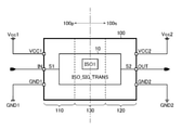
- FIG. 1 is a diagram showing a basic configuration example of a signal transmission device.
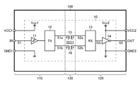
- FIG. 2 is a diagram showing a basic configuration example of an isolated signal transmission circuit.
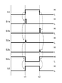
- FIG. 3 is a diagram showing a first example (normal time) of the isolated signal transmission operation.
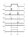
- FIG. 4 is a diagram showing a second example (when the set is abnormal) of the isolated signal transmission operation.
- FIG. 5 is a diagram showing a third example (at the time of reset abnormality) of the isolated signal transmission operation.
- FIG. 6 is a diagram showing a first embodiment of a signal transmission device.
- FIG. 7 is a diagram showing a first example (normal time) of the isolated signal transmission operation and the abnormality notification operation.
- FIG. 8 is a diagram showing a second example (when a set abnormality occurs) of the insulation signal transmission operation and the abnormality notification operation.
- FIG. 9 is a diagram showing a third example (at the time of reset abnormality) of the insulation signal transmission operation and the abnormality notification operation.
- FIG. 10 is a diagram showing a second embodiment of the signal transmission device.
- FIG. 11 is a diagram showing a third embodiment of the signal transmission device.
- FIG. 12 is a diagram showing a fourth embodiment of the signal transmission device.
- FIG. 13 is a diagram showing a fifth embodiment of the signal transmission device.
- FIG. 14 is a diagram showing a fourth example (normal time) of the isolated signal transmission operation and the abnormality notification operation.
- FIG. 15 is a diagram showing a fifth example (at the time of abnormality) of the insulation signal transmission operation and the abnormality notification operation.
- FIG. 16 is a diagram showing a sixth embodiment of the signal transmission device.
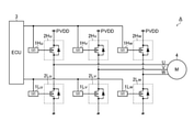
- FIG. 17 is a diagram showing an example of an electronic device equipped with a signal transmission device.
- FIG. 18 is a diagram showing only one phase of an electronic device extracted.
- FIG. 19 is a diagram showing the appearance of a vehicle on which an electronic device is mounted.
- FIG. 1 is a diagram showing a basic configuration example of a signal transmission device.
- the signal transmission device 100 of this configuration example has the primary circuit system 100p to the secondary circuit system 100s while insulating between the primary circuit system 100p (Vcc1-GND1 system) and the secondary circuit system 100s (Vcc2-GND2 system).
- It is a semiconductor integrated circuit device (so-called isolated gate driver IC) that transmits a pulse signal to and drives a gate of a power transistor (not shown) provided in the secondary circuit system 100s.
- the signal transduction device 100 has a plurality of external terminals (in this figure, a VCC1 pin, an IN pin, a GND1 pin, a VCS2 pin, an OUT pin, and a GND2) as means for establishing an electrical connection with the outside of the device.
- the pin is illustrated).
- the IN pin pulse signal input terminal
- the OUT pin (pulse signal output terminal) is connected to the gate of a power transistor (not shown).
- the signal transmission device 100 is used for all applications (motor drivers or DC / DC converters that handle high voltage, etc.) that require signal transmission between the primary circuit system 100p and the secondary circuit system 100s while insulating them from each other. ) Can be widely applied.
- the controller chip 110 is a semiconductor chip that integrates circuit elements of a primary circuit system 100p that operates by receiving a supply of a power supply voltage Vcc1 (for example, a maximum of 7V based on GND1).
- the driver chip 120 is a semiconductor chip in which circuit elements of the secondary circuit system 100s that operate by receiving a supply of a power supply voltage Vcc2 (for example, a maximum of 30V based on GND2) are integrated.
- the transformer chip 130 is a semiconductor chip in which a transformer for bidirectional signal transmission is integrated while insulating between the controller chip 110 and the driver chip 120.
- the signal transmission device 100 of this configuration example independently has a transformer chip 130 on which only a transformer is mounted, in addition to the controller chip 110 and the driver chip 120, and these three chips are packaged in a single package. It is sealed in.
- both the controller chip 110 and the driver chip 120 can be formed by a general low withstand voltage to medium withstand voltage process (withstand voltage of several V to several tens of V), and thus are dedicated. It is not necessary to use a high withstand voltage process (withstand voltage of several kV), and the manufacturing cost can be reduced.
- controller chip 110 and the driver chip 120 can be created by an existing process with a proven track record, and there is no need to perform a new reliability test, so that the development period can be shortened and the development cost can be reduced. It can contribute to the reduction.
- an insulating element other than the transformer for example, a capacitor or a photocoupler
- it can be easily dealt with by replacing only the transformer chip 130, so that the controller chip 110 and the driver chip 120 can be easily dealt with. It is not necessary to redevelop until then, which can contribute to shortening the development period and reducing the development cost.
- the signal transmission device 100 includes an isolated signal transmission circuit 10 as a main functional block.
- the isolated signal transmission circuit 10 insulates between the primary circuit system 100p and the secondary circuit system 100s via the first insulating element ISO1 (transformer or the like) integrated in the transformer chip 130, and the primary circuit system 100p. Transmits a pulse signal to the secondary circuit system 100s.
- the isolated signal transmission circuit 10 uses the input pulse signal S1 input to the IN pin of the primary circuit system 100p as the output pulse signal S2 output from the OUT pin of the secondary circuit system 100s. introduce.
- the circuit elements of the isolated signal transmission circuit 10 are dispersed and integrated in the controller chip 110, the driver chip 120, and the transformer chip 130 (details will be described later).
- FIG. 2 is a diagram showing a basic configuration example of the isolated signal transmission circuit 10.
- the isolated signal transmission circuit 10 of this configuration example includes a Schmid buffer 11, a pulse transmitting unit 12, a pulse receiving unit 13, a driver 14, and transformers 15 and 16 (corresponding to the first insulating element ISO 1 described above). include.
- the Schmidt buffer 11 is an example of waveform shaping means, and is connected between the IN pin and the pulse transmission unit 12.
- the pulse transmission unit 12 pulse-drives either one of the transmission pulse signals S1a and S1b according to the logic level of the input pulse signal S1 input from the IN pin via the Schmidt buffer 11.
- the pulse transmission unit 12 may drive a pulse signal S1a (single or multiple transmission pulses) applied to the primary winding 15p of the transformer 15 when notifying that the input pulse signal S1 is at a high level. Output) is performed to notify that the input pulse signal S1 is at a low level, and the transmission pulse signal S1b applied to the primary winding 16p of the transformer 16 is pulse-driven.
- the Schmidt buffer 11 and the pulse transmission unit 12 are both integrated in the controller chip 110 of the primary circuit system 100p (Vcc1-GND1 system).
- the pulse receiving unit 13 generates the received pulse signal S2c according to the received pulse signals S2a and S2b input from the transformers 15 and 16, respectively. For example, when the pulse receiving unit 13 receives the pulse drive of the transmitting pulse signal S1a and detects the induced pulse of the received pulse signal S2a appearing in the secondary winding 15s of the transformer 15, the received pulse signal S2c stands at a low level. Lower. On the other hand, when the pulse receiving unit 13 receives the pulse drive of the transmitting pulse signal S1b and detects the induced pulse of the received pulse signal S2b appearing in the secondary winding 16s of the transformer 16, the received pulse signal S2c stands at a high level. increase.
- the pulse receiving unit 13 and the driver 14 are both integrated in the driver chip 120 of the secondary circuit system 100s (Vcc2-GND2 system).
- the transformer 15 outputs the received pulse signal S2a from the secondary winding 15s in response to the transmission pulse signal S1a input to the primary winding 15p.
- the transformer 16 outputs the received pulse signal S2b from the secondary winding 16s in response to the transmission pulse signal S1b input to the primary winding 16p.
- the above transformers 15 and 16 are both integrated in the transformer chip 130.
- the transformer chip 130 uses transformers 15 and 16 to insulate between the controller chip 110 and the driver chip 120, and uses the transmission pulse signals S1a and S1b input from the pulse transmission unit 12 as the reception pulse signals S2a and S2b, respectively. It is output to the pulse receiving unit 13.
- FIG. 3 is a diagram showing a first example (normal time) of the isolated signal transmission operation by the isolated signal transmission circuit 10, in order from the top, the input pulse signal S1, the transmission pulse signal S1a and S1b, and the reception pulse signals S2a to S2c. , And the output pulse signal S2 is depicted.
- the description of the signal delay is omitted for convenience of explanation.
- the pulse transmission unit 12 drives the transmission pulse signal S1a at the rising edge of the input pulse signal S1 at time t1, while driving the transmission pulse signal S1b at the falling edge of the input pulse signal S1 at time t2.
- the pulse receiving unit 13 detects the induced pulse of the received pulse signal S2a generated by the pulse drive of the transmitted pulse signal S1a and lowers the received pulse signal S2c to a low level, while the received pulse signal generated by the pulse drive of the transmitted pulse signal S1b.
- the induced pulse of S2b is detected and the received pulse signal S2c is raised to a high level.
- the input pulse signal S1 can be transmitted as the output pulse signal S2. It disappears.
- FIG. 4 is a diagram showing a second example (when a set is abnormal) of the isolated signal transmission operation by the isolated signal transmission circuit 10, and is the same as in FIG. 3 above, in order from the top, the input pulse signal S1, the transmission pulse signal S1a, and the transmission pulse signal S1a. S1b, received pulse signals S2a to S2c, and output pulse signal S2 are depicted. In this figure, the description of the signal delay is omitted for convenience of explanation.
- the input pulse signal S1 rises to a high level at time t11, and even if the transmission pulse signal S1a is driven by the pulse, the induced pulse does not occur in the received pulse signal S2a. As a result, the received pulse signal S2c does not rise to the low level, so that the output pulse signal S2 does not rise to the high level.
- FIG. 5 is a diagram showing a third example (at the time of reset abnormality) of the isolated signal transmission operation by the isolated signal transmission circuit 10, and is the same as in FIG. 3 above, in order from the top, the input pulse signal S1, the transmission pulse signal S1a, and the transmission pulse signal S1a. S1b, received pulse signals S2a to S2c, and output pulse signal S2 are depicted. In this figure, the description of the signal delay is omitted for convenience of explanation.
- the input pulse signal S1 drops to a low level at time t22, and even if the transmission pulse signal S1b is driven by the pulse, the induced pulse does not occur in the received pulse signal S2b. As a result, the received pulse signal S2c does not rise to the high level, so that the output pulse signal S2 does not rise to the low level.
- the first insulating element ISO1 fails and the signal transmission from the primary circuit system 100p to the secondary circuit system 100s becomes impossible, the drive of the load provided in the secondary circuit system 100s is hindered.
- the signal transmission device 100 is used as a driving means of a motor mounted on a vehicle (particularly an electric vehicle such as an electric vehicle or a hybrid car), the control signal from the ECU is not transmitted to the power transistor.
- the motor that can be connected to the power transistor becomes uncontrollable.
- the basic safety mechanism of the vehicle such as running and stopping is impaired, which may lead to a serious accident.
- the first insulating element ISO1 that insulates between the primary circuit system 100p (Vcc1-GND1 system) and the secondary circuit system 100s (Vcc2-GND2 system) is used in a situation where it is easily damaged by being exposed to a strong electric field. Ru. Therefore, it can be said that the fail-safe function at the time of failure of the first insulating element ISO1 is extremely important.
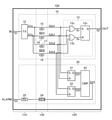
- FIG. 6 is a diagram showing a first embodiment of the signal transmission device 100.
- a fail-safe function using a plurality of insulating elements is added to the isolated signal transmission circuit 10 while being based on the above-mentioned basic configuration example (FIGS. 1 and 2).
- a new abnormality notification circuit 20 has been introduced separately.
- the Schmidt buffer 11 and the driver 14 mentioned above are omitted.
- the isolated signal transmission circuit 10 of the present embodiment includes a second insulating element ISO2 (transformers 17 and 18) in addition to the first insulating element ISO1 (transformers 15 and 16).
- the transformer 15 outputs the received pulse signal S2a1 from the secondary winding 15s in response to the transmission pulse signal S1a input to the primary winding 15p.
- the transformer 16 outputs the received pulse signal S2b1 from the secondary winding 16s in response to the transmission pulse signal S1b input to the primary winding 16p.
- the transformer 17 outputs the received pulse signal S2a2 from the secondary winding 17s in response to the transmission pulse signal S1a input to the primary winding 17p.
- the transformer 18 outputs the received pulse signal S2b2 from the secondary winding 18s in response to the transmission pulse signal S1b input to the primary winding 18p.
- the transformers 15 to 18 are all integrated into a single transformer chip 130.
- the pulse receiving unit 13 includes two OR gates 13x and 13y and one RS flip-flop 13z.
- the OR gate 13x generates a logical sum signal Sx of the received pulse signal S2a1 appearing in the secondary winding 15s of the transformer 15 and the received pulse signal S2a2 appearing in the secondary winding 17s of the transformer 17.
- the disjunction signal Sx becomes high level when at least one of the received pulse signals S2a1 and S2a2 is high level, and becomes low level when both the received pulse signals S2a1 and S2a2 are low level.
- the OR gate 13y generates a logical sum signal Sy of the received pulse signal S2b1 appearing in the secondary winding 16s of the transformer 16 and the received pulse signal S2b2 appearing in the secondary winding 18s of the transformer 18.
- the disjunction signal Sy becomes high level when at least one of the received pulse signals S2b1 and S2b2 is high level, and becomes low level when both the received pulse signals S2b1 and S2b2 are low level.
- waveform shaping means such as a Schmidt buffer may be arranged in front of each of the OR gates 13x and 13y.
- the RS flip-flop 13z is an output pulse signal output from the output end (Q) based on the OR signal Sx input to the set end (S) and the OR signal Sy input to the reset end (R).
- the logic level of S2 is switched. For example, the RS flip-flop 13z sets the output pulse signal S2 to a high level when the disjunction signal Sx rises to a high level, and resets the output pulse signal S2 to a low level when the disjunction signal Sy rises to a high level. do.
- the output end (Q) of the RS flip-flop 13z and the OUT pin are depicted as being directly connected, but a driver 14 such as an inverter or a buffer may be interposed.
- the signal transmission device 100 (particularly the isolated signal transmission circuit 10) of the present embodiment is provided in the primary circuit system 100p and is configured to generate transmission pulse signals S1a and S1b corresponding to the input pulse signal S1.
- ISO1 transformer
- One second insulating element ISO2 (transformers 17 and 18) and a first received pulse signal (S2a1 and S2b1) provided in the secondary circuit system 100s and output from the first insulating element ISO1 and the second insulating element ISO2, respectively.
- a pulse receiving unit configured to generate one output pulse signal S2 by inputting the second received pulse signal (S2a2 and S2b2) to the logic circuit (OR gate 13x and 13y, and RS flip flop 13z). 13 and.
- the pulse receiving unit 13 has, as the above-mentioned logic circuit, a combination circuit (OR gate, AND gate, etc.) that determines the output by the current input, and a sequential circuit (RS) that determines the output by the current input and the past input. Flip-flops or D-flip-flops, etc.) and may be included.
- the input pulse signal S1 of the primary circuit system 100p is used as the output pulse of the secondary circuit system 100s. Since it can be transmitted as the signal S2, it does not interfere with the driving of the load provided in the secondary circuit system 100s.
- the signal transmission device 100 is used as a driving means of a motor mounted on a vehicle (particularly an electric vehicle such as an electric vehicle or a hybrid car)
- the control signal from the ECU is correctly transmitted to the power transistor. Therefore, the control of the motor that can be connected to the power transistor can be continued. As a result, it is possible to maintain basic vehicle safety mechanisms such as running and stopping and avoid serious accidents.
- the number of insulating elements incorporated in the isolated signal transmission circuit 10 may be three or more. That is, the signal transmission paths for transmitting the transmission pulse signals S1a and S1b from the primary circuit system 100p to the secondary circuit system 100s, respectively, may be three or more systems.
- the logic level of the virtual output pulse signal S21 output from is switched. For example, the RS flip-flop 21 sets the virtual output pulse signal S21 to a high level when the received pulse signal S2a1 rises to a high level, and sets the virtual output pulse signal S21 to a low level when the received pulse signal S2b1 rises to a high level. Reset to.
- the RS flip-flop 22 (corresponding to the second sequential circuit) has an output end (Q) based on a received pulse signal S2a2 input to the set end (S) and a received pulse signal S2b2 input to the reset end (R).
- the logic level of the virtual output pulse signal S22 output from is switched. For example, the RS flip-flop 22 sets the virtual output pulse signal S22 to a high level when the received pulse signal S2a2 rises to a high level, and sets the virtual output pulse signal S22 to a low level when the received pulse signal S2b2 rises to a high level. Reset to.
- the signal comparison unit 23 outputs a comparison pulse signal S23 indicating a match / mismatch between the two signals by comparing the virtual output pulse signals S21 and S22.
- the comparison pulse signal S23 is transmitted from the primary circuit system 100p to the primary circuit system 100p.
- the abnormality notification circuit 20 is provided with a register for storing the signal value of the alarm signal S3, and a CPU [central processing unit] interface such as I 2C [inter-integrated circuit] or UART [universal asynchronous receiver / transmitter].
- a CPU [central processing unit] interface such as I 2C [inter-integrated circuit] or UART [universal asynchronous receiver / transmitter].
- an abnormality may be notified to the outside of the device by using an interface compliant with an in-vehicle communication standard such as LIN [local interconnect network] and CAN [controller area network].
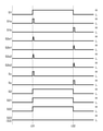
- FIG. 7 is a diagram showing a first example (normal time) of the isolated signal transmission operation and the abnormality notification operation, and in order from the top, the input pulse signal S1, the transmission pulse signals S1a and S1b, the reception pulse signals S2a1 and S2b1, and the reception are received.
- the pulse signals S2a2 and S2b2, the logical sum signals Sx and Sy, the output pulse signals S2, the virtual output pulse signals S21 and S22, and the comparison pulse signal S23 (and thus the alarm signal S3) are depicted.
- the description of the signal delay is omitted for convenience of explanation.
- the pulse transmission unit 12 drives the transmission pulse signal S1a at the rising edge of the input pulse signal S1 at time t31, while driving the transmission pulse signal S1b at the falling edge of the input pulse signal S1 at time t32.
- an induced pulse is generated in both the received pulse signals S2a1 and S2a2 at time t31, so that the OR signal Sx becomes a high level. stand up. Further, at time t32, an induced pulse is generated in both the received pulse signals S2b1 and S2b2, so that the disjunction signal Sy rises to a high level.
- the output pulse signal S2 when the input pulse signal S1 rises to a high level, the output pulse signal S2 also rises to a high level, and conversely, when the input pulse signal S1 falls to a low level, the output pulse signal is matched accordingly. S2 also falls to the low level.
- the virtual output pulse signals S21 and S22 are both high due to the induced pulses of the received pulse signals S2a1 and S2a2 at time t31. While rising to the level, at time t32, the virtual output pulse signals S21 and S22 both fall to the low level due to the induced pulses of the received pulse signals S2b1 and S2b2, respectively. That is, since the logic levels of the virtual output pulse signals S21 and S22 are the same, the comparison pulse signal S23 (and thus the alarm signal S3) becomes a low level.
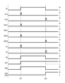
- FIG. 8 is a diagram showing a second example (when a set abnormality occurs) of the isolated signal transmission operation and the abnormality notification operation, and is the same as in FIG. 7 above, in order from the top, the input pulse signal S1, the transmission pulse signal S1a, and S1b. , Received pulse signals S2a1 and S2b1, received pulse signals S2a2 and S2b2, logical sum signals Sx and Sy, output pulse signals S2, virtual output pulse signals S21 and S22, and comparison pulse signals S23 (and alarm signal S3). It is depicted. In this figure, the description of the signal delay is omitted for convenience of explanation.
- an induced pulse is generated in the received pulse signal S2a1 even if the input pulse signal S1 rises to a high level and the transmission pulse signal S1a is driven by the pulse at time t41. It disappears.
- the transformer 17 is not out of order, an induced pulse is generated in the received pulse signal S2a2, so that the disjunction signal Sx rises to a high level. Therefore, the output pulse signal S2 rises to a high level without any trouble.
- the virtual output pulse signal S21 does not rise to a high level unless an induced pulse is generated in the received pulse signal S2a1.
- the logic levels of the virtual output pulse signals S21 and S22 do not match, so that the comparison pulse signal S23 (and thus the alarm signal S3) rises to a high level at time t41.
- FIG. 9 is a diagram showing a third example (at the time of reset abnormality) of the isolated signal transmission operation and the abnormality notification operation, and is the same as in FIGS. 7 and 8 above, in order from the top, the input pulse signal S1 and the transmission pulse signal S1a. S1b, received pulse signals S2a1 and S2b1, received pulse signals S2a2 and S2b2, logical sum signals Sx and Sy, output pulse signal S2, virtual output pulse signals S21 and S22, and comparison pulse signal S23 (and alarm signal S3). ) Is depicted. In this figure, the description of the signal delay is omitted for convenience of explanation.
- the input pulse signal S1 drops to a low level at time t52, and even if the transmission pulse signal S1b is driven by the pulse, the induced pulse is generated in the received pulse signal S2b1. It will not occur.
- the transformer 18 is not out of order, an induced pulse is generated in the received pulse signal S2b2, so that the disjunction signal Sy rises to a high level. Therefore, the output pulse signal S2 falls to a low level without any trouble.
- the virtual output pulse signal S21 does not fall to the low level unless an induced pulse is generated in the received pulse signal S2b1.
- the logic levels of the virtual output pulse signals S21 and S22 do not match, so that the comparison pulse signal S23 (and thus the alarm signal S3) rises to a high level at time t52.
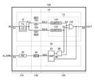
- FIG. 10 is a diagram showing a second embodiment of the signal transmission device 100.
- the signal transmission device 100 of the present embodiment is based on the first embodiment (FIG. 6) described above, but the internal configuration of the abnormality notification circuit 20 has been changed.
- the abnormality notification circuit 20 includes AND gates 26 to 29 and an OR gate 2A in place of the RS flip-flops 21 and 22 and the signal comparison unit 23 described above.
- the AND gate 26 generates a logical product signal S26 of the received pulse signal S2a1 and the received pulse signal S2a2.
- the AND signal S26 becomes low level when at least one of the received pulse signals S2a1 and S2a2 is low level, and becomes high level when both the received pulse signals S2a1 and S2a2 are high level.
- the AND gate 27 generates a logical product signal S27 of the received pulse signal S2b1 and the received pulse signal S2b2.
- the AND signal S27 becomes low level when at least one of the received pulse signals S2b1 and S2b2 is low level, and becomes high level when both the received pulse signals S2b1 and S2b2 are high level.
- waveform shaping means such as a Schmidt buffer may be arranged in front of each of the AND gates 26 and 27.
- the AND gate 28 generates a logical product signal S28 of the logical sum signal Sx and the logical product signal S26.
- the logical product signal S28 becomes low level when at least one of the logical sum signal Sx and the logical product signal S26 is low level, and becomes high level when both the logical sum signal Sx and the logical product signal S26 are high level. Become.
- the AND gate 29 generates a logical product signal S29 of the logical sum signal Sy and the logical product signal S27.
- the logical product signal S29 becomes low level when at least one of the logical sum signal Sy and the logical product signal S27 is low level, and becomes high level when both the logical sum signal Sy and the logical product signal S27 are high level. Become.
- the OR gate 2A generates an OR signal SA of the AND signal S28 and the AND signal S29.
- the disjunction signal SA becomes high level when at least one of the AND signals S28 and S29 is high level, and becomes low level when both the AND signals S28 and S29 are low level.
- the logical sum signal SA is transmitted from the primary circuit system to the primary circuit system 100p.
- the pulse receiving unit 25 generates an alarm signal S3 corresponding to the OR signal SA input via the insulating element 24 and outputs it from the ALARM pin to the outside of the device (ECU or the like).
- a pulse is generated in the alarm signal S3 every time the logic level of the input pulse signal S1 is switched.
- pulse omission of the alarm signal S3 occurs.
- FIG. 11 is a diagram showing a third embodiment of the signal transmission device 100.
- the signal transduction device 100 of the present embodiment is based on the first embodiment (FIG. 6) or the second embodiment (FIG. 10) described above, and instead of the single transchip 130, a plurality of transchips 130x. And 130y are packaged.
- the first insulating element ISO1 (transformers 15 and 16) may be integrated in the transformer chip 130x.
- the second insulating element ISO2 (transformers 17 and 18) may be integrated in the transformer chip 130y.
- the first insulating element ISO1 and the second insulating element ISO2 are less likely to be destroyed at the same time. Therefore, it is possible to enhance the safety of the signal transmission device 100.
- FIG. 12 is a diagram showing a fourth embodiment of the signal transmission device 100.
- the transformers 15 to 18 are replaced with capacitors 19 to 1C, respectively, based on the first embodiment (FIG. 6) described above.
- the first insulating element ISO1 and the second insulating element ISO2 are not necessarily limited to transformers, but may be capacitors. Further, although not shown again, the first insulating element ISO1 and the second insulating element ISO2 may be photocouplers.
- FIG. 13 is a diagram showing a fifth embodiment of the signal transmission device 100.
- the signal transmission device 100 of the present embodiment is based on the first embodiment (FIG. 6) described above, and has a signal modulation function incorporated in the pulse transmission unit 12, and along with this, various post-stage circuits also have various functions. Changes have been made.
- the pulse transmission unit 12 includes an OK [on-off keying] method (a type of ASK [amplitude-shift keying] method) modulator, and responds to the input pulse signal S1.
- OK [on-off keying] method a type of ASK [amplitude-shift keying] method
- the transformer 1Da outputs the received pulse signal S2c1 from the secondary winding 1Da in response to the transmission pulse signal S1c input to the primary winding 1Dap.
- the transformer 1Db outputs the received pulse signal S2c2 from the secondary winding 1Dbs in response to the transmission pulse signal S1c input to the primary winding 1Dbp.
- the pulse receiving unit 13 includes demodulators 13X and 13Y and an OR gate 13Z.
- the demodulator 13X generates a demodulated pulse signal SX by performing a predetermined demodulation process on the received pulse signal S2c1.
- the demodulator 13X generates a demodulated pulse signal SY by performing a predetermined demodulation process on the received pulse signal S2c1.
- the OR gate 13Z generates an output pulse signal S2 by a logical sum operation of the demodulated pulse signal SX and the demodulated pulse signal SY. Therefore, the output pulse signal S2 becomes high level when at least one of the demodulated pulse signals SX and SY is high level, and becomes low level when both the demodulated pulse signals SX and SY are low level.
- the signal transmission device 100 (particularly the isolated signal transmission circuit 10) of the present embodiment includes a pulse transmission unit 12 provided in the primary circuit system 100p to generate a transmission pulse signal S1c corresponding to the input pulse signal S1.
- the first insulating element ISO1 (transformer 1Da) forming the first signal transmission path for transmitting the transmission pulse signal S1c from the primary circuit system 100p to the secondary circuit system 100s, and the transmission pulse signal S1c are transmitted from the primary circuit system 100p to the second.
- a second insulating element ISO2 (transformer 1Db) that forms a second signal transmission path different from the above first signal transmission path for transmission to the secondary circuit system 100s, and a first insulation provided in the secondary circuit system 100s. It has a pulse receiving unit 13 that generates one output pulse signal S2 by inputting received pulse signals S2c1 and S2c2 output from the element ISO1 and the second insulating element ISO2 to a logic circuit (OR gate 13Z), respectively.
- the input pulse signal S1 of the primary circuit system 100p is used as the output pulse of the secondary circuit system 100s. Since it can be transmitted as the signal S2, it does not interfere with the driving of the load provided in the secondary circuit system 100s.
- the abnormality notification circuit 20 includes an AND gate 2B instead of the RS flip-flops 21 and 22 described above.
- the AND gate 2Z generates a AND signal SB of the demodulated pulse signal SX and the demodulated pulse signal SY.
- the logical product signal SB becomes low level when at least one of the demodulated pulse signal SX and the demodulated pulse signal SY is low level, and becomes high level when both the demodulated pulse signal SX and the demodulated pulse signal SY are high level. Become.
- the signal comparison unit 23 outputs a comparison pulse signal S23 indicating a match / mismatch between the output pulse signal S2 and the AND signal SB by comparing the output pulse signal S2 with the AND signal SB.
- the insulating element 24 transmits the comparative pulse signal S23 from the secondary circuit system 100s to the primary circuit system 100p while insulating between the primary circuit system 100p and the secondary circuit system 100s.
- the pulse receiving unit 25 generates an alarm signal S3 corresponding to the comparison pulse signal S23 input via the insulating element 24 and outputs the alarm signal S3 from the ALARM pin to the outside of the device (ECU or the like).
- FIG. 14 is a diagram showing a fourth example (normal time) of the isolated signal transmission operation and the abnormality notification operation, and is an input pulse signal S1, a transmission pulse signal S1c, a reception pulse signal S2c1 and S2c1, and a demodulation pulse signal in order from the top.
- the SX and SY, the output pulse signal S2, the logical product signal SB, and the comparison pulse signal S23 (and thus the alarm signal S3) are depicted.
- the description of the signal delay is omitted for convenience of explanation.
- FIG. 15 is a diagram showing a fifth example (at the time of abnormality) of the isolated signal transmission operation and the abnormality notification operation, and is the same as in FIG. 14 above, in order from the top, the input pulse signal S1, the transmission pulse signal S1c, and the reception pulse.
- the signals S2c1 and S2c1, the demodulated pulse signals SX and SY, the output pulse signal S2, the logical product signal SB, and the comparative pulse signal S23 (and thus the alarm signal S3) are depicted.
- the description of the signal delay is omitted for convenience of explanation.
- the second insulating element ISO2 is not faulty, an induced pulse is generated in the received pulse signal S2c2, so that the demodulated pulse signal SY rises to a high level. Therefore, the output pulse signal S2 rises to a high level without any trouble.
- the AND signal SB does not rise to a high level because the demodulated pulse signal SX remains at a low level.
- the logic levels of the output pulse signal S2 and the AND signal SB do not match, so that the comparison pulse signal S23 (and thus the alarm signal S3) rises to a high level at times t71 to t72.
- the output pulse signal S2 rises to a high level without any trouble.
- FIG. 16 is a diagram showing a sixth embodiment of the signal transmission device 100.
- the transformers 1Da and 1Db are replaced with capacitors 1Ea and 1Eb, respectively, based on the fifth embodiment (FIG. 13) described above.
- the first insulating element ISO1 and the second insulating element ISO2 are not necessarily limited to transformers, but may be capacitors. Further, although not shown again, the first insulating element ISO1 and the second insulating element ISO2 may be photocouplers.
- FIG. 17 is a diagram showing a configuration example of an electronic device on which the signal transmission device 100 is mounted.
- the electronic device A of this configuration example includes an upper gate driver IC1H (u / v / w), a lower gate driver IC1L (u / v / w), an upper power transistor 2H (u / v / w), and a lower part. It has a side power transistor 2L (u / v / w), an ECU 3, and a motor 4.
- the upper gate driver IC1H (u / v / w) and the lower gate driver IC1L (u / v / w) are used as the signal transmission according to any one of the first to sixth embodiments described above.
- Device 100 is used.
- the lower power transistor 2L (u / v / w) serves as a lower switch forming a three-phase (U-phase / V-phase / W-phase) half-bridge output stage, respectively, with each phase input end of the motor 4 and power. It is connected to the system grounding end.
- N-channel MOSFETs metal oxide semiconductor field effect transistors
- a P-channel type MOSFET may be used as the upper power transistor 2H (u / v / w).
- an IGBT insulated gate bipolar transistor] can be used instead of the MOSFET.
- a device using a wide bandgap semiconductor SiC device or GaN). A device, etc. may be used.
- the ECU 3 has an upper power transistor 2H (u / v / w) and a lower power transistor 2L (u) via the upper gate driver IC1H (u / v / w) and the lower gate driver IC1L (u / v / w).
- the ECU 3 is based on the alarm signal S3 input from the abnormality notification circuit 20 (not shown) of each of the upper gate driver IC1H (u / v / w) and the lower gate driver IC1L (u / v / w). It also has a function to perform various safety controls.
- the motor 4 is a three-phase motor that is rotationally driven according to the three-phase drive voltage U / V / W input from each of the three-phase (U-phase / V-phase / W-phase) half-bridge output stages.
- FIG. 18 is a diagram showing only one phase of the electronic device A extracted.
- the IN pin and ALARM pin of the upper gate driver IC1H and the lower gate driver IC1L are connected to the ECU 3.
- the OUT pins of the upper gate driver IC1H and the lower gate driver IC1L are connected to the gates of the upper power transistor 2H and the lower power transistor 2L, respectively.
- the ECU 3 can grasp the presence or absence of an abnormality in signal transmission based on the alarm signal S3 input from each of the upper gate driver IC1H and the lower gate driver IC1L, and implement appropriate safety control. It will be possible.
- FIG. 19 is a diagram showing the appearance of a vehicle on which an electronic device is mounted.
- the vehicle X of this configuration example is equipped with a battery (not shown in this figure) and various electronic devices X11 to X18 that operate by receiving electric power from the battery.
- Vehicle X includes engine vehicles, electric vehicles (BEV [battery electric vehicle], HEV [hybrid electric vehicle], PHEV / PHV (plug-in hybrid electric vehicle / plug-in hybrid vehicle), or FCEV / FCV.
- BEV battery electric vehicle
- HEV battery electric vehicle
- PHEV / PHV plug-in hybrid electric vehicle / plug-in hybrid vehicle
- FCEV / FCV FCV
- XEV such as fuel cell electric vehicle / fuel cell vehicle
- the electronic device X11 is engine-related control (injection control, electronic throttle control, idling control, oxygen sensor heater control, auto-cruise control, etc.) or motor-related control (torque control, power regeneration control, etc.). It is an electronic control unit that performs.
- the electronic device X12 is a lamp control unit that controls turning on and off such as HID [high intensity discharged lamp] and DRL [daytime running lamp].
- the electronic device X13 is a transmission control unit that performs control related to the transmission.
- the electronic device X14 is a braking unit that performs control related to the movement of the vehicle X (ABS [anti-lock brake system] control, EPS [electric power steering] control, electronic suspension control, etc.).
- ABS anti-lock brake system
- EPS electric power steering
- electronic suspension control etc.
- the electronic device X15 is a security control unit that controls drive such as a door lock and a security alarm.
- the electronic device X16 is an electronic device incorporated in the vehicle X at the factory shipment stage as a standard equipment or a manufacturer's option such as a wiper, an electric door mirror, a power window, a damper (shock absorber), an electric sunroof, and an electric seat. Is.
- the electronic device X17 is an electronic device that is optionally mounted on the vehicle X as a user option such as an in-vehicle A / V [audio / visual] device, a car navigation system, and an ETC [electronic toll collection system].
- the electronic device X18 is an electronic device equipped with a high withstand voltage motor such as an in-vehicle blower, an oil pump, a water pump, and a battery cooling fan.
- a high withstand voltage motor such as an in-vehicle blower, an oil pump, a water pump, and a battery cooling fan.
- the electronic devices X11 to X18 can be understood as specific examples of the electronic device A described above. That is, the signal transmission device 100 described above can be incorporated into any of the electronic devices X11 to X18.
- the signal transmission device disclosed in the present specification includes a transmission unit provided in the primary circuit system and configured to generate a transmission signal corresponding to an input signal, and the transmission signal in the primary circuit system.
- At least one first insulating element configured to form a first signal transmission path for transmission from to the secondary circuit system, and to transmit the transmission signal from the primary circuit system to the secondary circuit system.
- At least one second insulating element configured to form a second signal transmission path different from the first signal transmission path, and the first insulating element and the second insulating element provided in the secondary circuit system. It is configured to have a receiving unit configured to input the first received signal and the second received signal output from the insulating element to the logic circuit to generate one output signal (first configuration). ing.
- the logic circuit determines the output by the combination circuit configured to determine the output by the current input and the current input and the past input.
- the configuration (second configuration) may include at least one of the sequential circuits configured in.
- the signal transmission device having the first or second configuration monitors both the first received signal and the second received signal, and an alarm indicating an abnormality of either the first insulating element or the second insulating element.
- the configuration (third configuration) may further include an abnormality notification circuit configured to generate a signal.
- the abnormality notification circuit is provided in the secondary circuit system and is configured to generate a first virtual output signal from the first received signal.
- a signal comparison unit configured to generate a comparison signal by comparing a virtual output signal and the second virtual output signal, and a configuration to transmit the comparison signal from the secondary circuit system to the primary circuit system.
- a third insulating element is provided, and an alarm signal generation unit provided in the primary circuit system and configured to generate the alarm signal in response to the comparison signal input via the third insulating element.
- the configuration may include (fourth configuration).
- the transmission unit may have a configuration (fifth configuration) in which the amplitude of the transmission signal is changed according to the input signal.
- the transmission unit may have a configuration (sixth configuration) including an ASK [amplitude-shift keying] type modulator.
- the transmission unit may have a configuration (seventh configuration) including an OK [on-off keying] type modulator.
- the first chip in which the circuit elements of the primary circuit system are integrated and the second chip in which the circuit elements of the secondary circuit system are integrated are integrated.
- at least one third chip in which the first insulating element and the second insulating element are integrated may be sealed in a single package (eighth configuration).
- the first insulating element and the second insulating element are both integrated into a single third chip (9th configuration). Configuration) may be used.
- the first insulating element and the second insulating element are each dispersed and integrated in a plurality of the third chips (10th configuration). You may do it.
- the plurality of the third chips may all have the same structure (11th configuration).
- the first insulating element and the second insulating element are both transformers, capacitors or photocouplers (12th configuration). good.
- the electronic device disclosed in the present specification includes a power transistor and a gate driver IC configured to drive the gate of the power transistor, and the gate driver IC is the above-mentioned first.
- the configuration is a signal transmission device having any of the first to twelfth configurations (thirteenth configuration).
- the vehicle disclosed in the present specification has a configuration (14th configuration) having an electronic device having the above-mentioned thirteenth configuration.
Landscapes
- Engineering & Computer Science (AREA)
- Power Engineering (AREA)
- Computer Hardware Design (AREA)
- Physics & Mathematics (AREA)
- Computing Systems (AREA)
- General Engineering & Computer Science (AREA)
- Mathematical Physics (AREA)
- Dc Digital Transmission (AREA)
Abstract
Description
図1は信号伝達装置の基本構成例を示す図である。本構成例の信号伝達装置100は、一次回路系100p(Vcc1-GND1系)と二次回路系100s(Vcc2-GND2系)との間を絶縁しつつ、一次回路系100pから二次回路系100sにパルス信号を伝達し、二次回路系100sに設けられたパワートランジスタ(不図示)のゲートを駆動する半導体集積回路装置(いわゆる絶縁ゲートドライバIC)である。
図2は、絶縁信号伝達回路10の基本構成例を示す図である。本構成例の絶縁信号伝達回路10は、シュミットバッファ11と、パルス送信部12と、パルス受信部13と、ドライバ14と、トランス15及び16(先出の第1絶縁素子ISO1に相当)とを含む。
図3は、絶縁信号伝達回路10による絶縁信号伝達動作の第1例(正常時)を示す図であり、上から順に、入力パルス信号S1、送信パルス信号S1a並びにS1b、受信パルス信号S2a~S2c、及び、出力パルス信号S2が描写されている。本図では、説明の便宜上、信号遅延の描写が省略されている。
図6は、信号伝達装置100の第1実施形態を示す図である。本実施形態の信号伝達装置100では、先出の基本構成例(図1及び図2)を基本としつつ、絶縁信号伝達回路10に複数の絶縁素子を用いたフェイルセーフ機能が追加されると共に、別途新たに異常報知回路20が導入されている。なお、本図では、先出のシュミットバッファ11とドライバ14が省略されている。
図7は、絶縁信号伝達動作及び異常報知動作の第1例(正常時)を示す図であり、上から順に、入力パルス信号S1、送信パルス信号S1a並びにS1b、受信パルス信号S2a1並びにS2b1、受信パルス信号S2a2並びにS2b2、論理和信号Sx並びにSy、出力パルス信号S2、仮想出力パルス信号S21並びにS22、及び、比較パルス信号S23(延いてはアラーム信号S3)が描写されている。本図では、説明の便宜上、信号遅延の描写が省略されている。
図10は、信号伝達装置100の第2実施形態を示す図である。本実施形態の信号伝達装置100は、先出の第1実施形態(図6)を基本としつつ、異常報知回路20の内部構成が変更されている。本図に即して述べると、異常報知回路20は、先出のRSフリップフロップ21及び22と信号比較部23に代えて、ANDゲート26~29とORゲート2Aを含む。
図11は、信号伝達装置100の第3実施形態を示す図である。本実施形態の信号伝達装置100では、先出の第1実施形態(図6)または第2実施形態(図10)を基本としつつ、単一のトランスチップ130に代えて、複数のトランスチップ130x及び130yがパッケージングされている。
図12は、信号伝達装置100の第4実施形態を示す図である。本実施形態の信号伝達装置100は、先出の第1実施形態(図6)を基本としつつ、トランス15~18がそれぞれキャパシタ19~1Cに置換されている。
図13は、信号伝達装置100の第5実施形態を示す図である。本実施形態の信号伝達装置100は、先出の第1実施形態(図6)を基本としつつ、パルス送信部12に信号変調機能が組み込まれており、これに伴って後段回路にも種々の変更が加えられている。
図14は、絶縁信号伝達動作及び異常報知動作の第4例(正常時)を示す図であり、上から順に、入力パルス信号S1、送信パルス信号S1c、受信パルス信号S2c1並びにS2c1、復調パルス信号SX及びSY、出力パルス信号S2、論理積信号SB、及び、比較パルス信号S23(延いてはアラーム信号S3)が描写されている。本図では、説明の便宜上、信号遅延の描写が省略されている。
図16は、信号伝達装置100の第6実施形態を示す図である。本実施形態の信号伝達装置100は、先出の第5実施形態(図13)を基本としつつ、トランス1Da及び1Dbがそれぞれキャパシタ1Ea及び1Ebに置換されている。
図17は、信号伝達装置100が搭載される電子機器の一構成例を示す図である。本構成例の電子機器Aは、上側ゲートドライバIC1H(u/v/w)と、下側ゲートドライバIC1L(u/v/w)と、上側パワートランジスタ2H(u/v/w)と、下側パワートランジスタ2L(u/v/w)と、ECU3と、モータ4と、を有する。
図19は、電子機器が搭載される車両の外観を示す図である。本構成例の車両Xは、バッテリ(本図では不図示)と、バッテリから電力供給を受けて動作する種々の電子機器X11~X18と、を搭載している。
以下では、これまでに説明してきた種々の実施形態について総括的に述べる。
なお、本明細書中に開示されている種々の技術的特徴は、上記実施形態のほか、その技術的創作の主旨を逸脱しない範囲で種々の変更を加えることが可能である。すなわち、上記実施形態は、全ての点で例示であって制限的なものではないと考えられるべきであり、本発明の技術的範囲は、特許請求の範囲の記載により規定されるものであって、特許請求の範囲と均等の意味及び範囲内に属する全ての変更が含まれると理解されるべきである。
1L(u/v/w) 下側ゲートドライバIC
2H(u/v/w) 上側パワートランジスタ
2L(u/v/w) 下側パワートランジスタ
3 ECU
4 モータ
10 絶縁信号伝達回路
11 シュミットバッファ
12 パルス送信部
13 パルス受信部
13x、13y ORゲート
13z RSフリップフロップ
13X、13Y 復調器
13Z ORゲート
14 ドライバ
15、16、17、18、1Da、1Db トランス
15p、16p、17p、18p、1Dap、1Dbp 一次巻線
15s、16s、17s、18s、1Das、1Dbs 二次巻線
19、1A、1B、1C、1Ea、1Eb キャパシタ
20 異常報知回路
21、22 RSフリップフロップ
23 信号比較部
24 絶縁素子
25 パルス受信部
26、27、28、29、2B ANDゲート
2A ORゲート
100 信号伝達装置(絶縁ゲートドライバIC)
100p 一次回路系
100s 二次回路系
110 コントローラチップ
120 ドライバチップ
130、130x、130y トランスチップ
A 電子機器
ISO1 第1絶縁素子
ISO2 第2絶縁素子
ISO3 第3絶縁素子
X 車両
X11~X18 電子機器
Claims (14)
- 一次回路系に設けられて入力信号に応じた送信信号を生成するように構成された送信部と、
前記送信信号を前記一次回路系から二次回路系に伝達するために第1信号伝達経路を形成するように構成された少なくとも一つの第1絶縁素子と、
前記送信信号を前記一次回路系から前記二次回路系に伝達するために前記第1信号伝達経路とは異なる第2信号伝達経路を形成するように構成された少なくとも一つの第2絶縁素子と、
前記二次回路系に設けられて前記第1絶縁素子及び前記第2絶縁素子からそれぞれ出力される第1受信信号及び第2受信信号を論理回路に入力して一つの出力信号を生成するように構成された受信部と、
を有する、信号伝達装置。 - 前記論理回路は、現在の入力で出力を決定するように構成された組み合わせ回路、及び、現在の入力と過去の入力で出力を決定するように構成された順序回路の少なくとも一方を含む、請求項1に記載の信号伝達装置。
- 前記第1受信信号及び前記第2受信信号の双方を監視して前記第1絶縁素子及び前記第2絶縁素子いずれかの異常を示すアラーム信号を生成するように構成された異常報知回路をさらに有する、請求項1または2に記載の信号伝達装置。
- 前記異常報知回路は、
前記二次回路系に設けられて前記第1受信信号から第1仮想出力信号を生成するように構成された第1順序回路と、
前記二次回路系に設けられて前記第2受信信号から第2仮想出力信号を生成するように構成された第2順序回路と、
前記二次回路系に設けられて前記第1仮想出力信号及び前記第2仮想出力信号を比較することにより比較信号を生成するように構成された信号比較部と、
前記二次回路系から前記一次回路系に前記比較信号を伝達するように構成された第3絶縁素子と、
前記一次回路系に設けられて前記第3絶縁素子経由で入力される前記比較信号に応じて前記アラーム信号を生成するように構成されたアラーム信号生成部と、
を含む、請求項3に記載の信号伝達装置。 - 前記送信部は、前記入力信号に応じて前記送信信号の振幅を変化させる、請求項1~4のいずれか一項に記載の信号伝達装置。
- 前記送信部は、ASK[amplitude-shift keying]方式の変調器を含む、請求項5に記載の信号伝達装置。
- 前記送信部は、OOK[on-off keying]方式の変調器を含む、請求項5に記載の信号伝達装置。
- 前記一次回路系の回路素子を集積化した第1チップと、
前記二次回路系の回路素子を集積化した第2チップと、
前記第1絶縁素子及び前記第2絶縁素子を集積化した少なくとも一つの第3チップと、
を単一のパッケージに封止した、請求項1~7のいずれか一項に記載の信号伝達装置。 - 前記第1絶縁素子及び前記第2絶縁素子は、いずれも単一の前記第3チップに集約して集積化されている、請求項8に記載の信号伝達装置。
- 前記第1絶縁素子及び前記第2絶縁素子は、それぞれ複数の前記第3チップに分散して集積化されている、請求項8に記載の信号伝達装置。
- 複数の前記第3チップはいずれも同一構造である、請求項10に記載の信号伝達装置。
- 前記第1絶縁素子及び前記第2絶縁素子は、いずれもトランス、キャパシタまたはフォトカプラである、請求項1~11のいずれか一項に記載の信号伝達装置。
- パワートランジスタと、前記パワートランジスタのゲートを駆動するように構成されたゲートドライバICと、を有し、前記ゲートドライバICは、請求項1~12のいずれか一項に記載の信号伝達装置である、電子機器。
- 請求項13に記載の電子機器を有する、車両。
Priority Applications (5)
| Application Number | Priority Date | Filing Date | Title |
|---|---|---|---|
| DE112021003377.8T DE112021003377T5 (de) | 2020-09-03 | 2021-08-23 | Signalübertragungseinrichtung, elektronische vorrichtung und fahrzeug |
| CN202180054652.1A CN116114226A (zh) | 2020-09-03 | 2021-08-23 | 信号传输装置、电子设备、车辆 |
| US18/018,409 US12407334B2 (en) | 2020-09-03 | 2021-08-23 | Signal transmission device, electronic device, vehicle |
| JP2022546243A JPWO2022050102A1 (ja) | 2020-09-03 | 2021-08-23 | |
| US19/272,767 US20250343534A1 (en) | 2020-09-03 | 2025-07-17 | Signal transmission device, electronic device, vehicle |
Applications Claiming Priority (2)
| Application Number | Priority Date | Filing Date | Title |
|---|---|---|---|
| JP2020148119 | 2020-09-03 | ||
| JP2020-148119 | 2020-09-03 |
Related Child Applications (2)
| Application Number | Title | Priority Date | Filing Date |
|---|---|---|---|
| US18/018,409 A-371-Of-International US12407334B2 (en) | 2020-09-03 | 2021-08-23 | Signal transmission device, electronic device, vehicle |
| US19/272,767 Continuation US20250343534A1 (en) | 2020-09-03 | 2025-07-17 | Signal transmission device, electronic device, vehicle |
Publications (1)
| Publication Number | Publication Date |
|---|---|
| WO2022050102A1 true WO2022050102A1 (ja) | 2022-03-10 |
Family
ID=80490885
Family Applications (1)
| Application Number | Title | Priority Date | Filing Date |
|---|---|---|---|
| PCT/JP2021/030759 Ceased WO2022050102A1 (ja) | 2020-09-03 | 2021-08-23 | 信号伝達装置、電子機器、車両 |
Country Status (5)
| Country | Link |
|---|---|
| US (2) | US12407334B2 (ja) |
| JP (1) | JPWO2022050102A1 (ja) |
| CN (1) | CN116114226A (ja) |
| DE (1) | DE112021003377T5 (ja) |
| WO (1) | WO2022050102A1 (ja) |
Families Citing this family (4)
| Publication number | Priority date | Publication date | Assignee | Title |
|---|---|---|---|---|
| US20240096538A1 (en) * | 2021-01-29 | 2024-03-21 | Rohm Co., Ltd. | Transformer chip and signal transmission device |
| US11916064B2 (en) * | 2021-09-28 | 2024-02-27 | Monolithic Power Systems, Inc. | Integrated circuit with fault reporting structure |
| CN117439559B (zh) * | 2023-10-20 | 2024-05-17 | 哈尔滨海鸿基业科技发展有限公司 | 一种隔离脉冲的功率放大电路及控制方法 |
| TWI911006B (zh) * | 2024-12-02 | 2026-01-01 | 晶焱科技股份有限公司 | 具有額外延遲的數位隔離器電路 |
Citations (3)
| Publication number | Priority date | Publication date | Assignee | Title |
|---|---|---|---|---|
| JP2009094576A (ja) * | 2007-10-03 | 2009-04-30 | Toyota Industries Corp | 信号伝達回路 |
| JP2015015697A (ja) * | 2013-06-07 | 2015-01-22 | ローム株式会社 | 信号伝達装置 |
| JP2018011108A (ja) * | 2016-07-11 | 2018-01-18 | 三菱電機株式会社 | 信号伝達装置、および、電力スイッチング素子駆動装置 |
Family Cites Families (9)
| Publication number | Priority date | Publication date | Assignee | Title |
|---|---|---|---|---|
| JP3931500B2 (ja) * | 1999-09-22 | 2007-06-13 | 松下電器産業株式会社 | 非接触icカードおよびそのデータ処理方法 |
| US8198951B2 (en) | 2004-06-03 | 2012-06-12 | Silicon Laboratories Inc. | Capacitive isolation circuitry |
| US8477856B2 (en) * | 2009-03-31 | 2013-07-02 | Analog Devices, Inc. | Multi-bit digital signal isolator |
| CN105790744B (zh) * | 2009-11-05 | 2019-09-03 | 罗姆股份有限公司 | 半导体器件、检查半导体器件的方法和装置 |
| JP5926003B2 (ja) | 2011-06-10 | 2016-05-25 | ローム株式会社 | 信号伝達装置及びこれを用いたモータ駆動装置 |
| JP5947633B2 (ja) * | 2012-06-22 | 2016-07-06 | ローム株式会社 | 信号伝達回路、集積回路およびそれを含む電気機器 |
| US9698728B2 (en) * | 2012-12-13 | 2017-07-04 | Texas Instruments Incorporated | Digital isolator |
| US9257836B2 (en) | 2013-12-19 | 2016-02-09 | Silicon Laboratories Inc. | Suppression of transients in communications across an isolation barrier |
| US11792051B2 (en) * | 2020-07-17 | 2023-10-17 | Texas Instruments Incorporated | Multi-channel digital isolator with integrated configurable pulse width modulation interlock protection |
-
2021
- 2021-08-23 DE DE112021003377.8T patent/DE112021003377T5/de active Pending
- 2021-08-23 CN CN202180054652.1A patent/CN116114226A/zh active Pending
- 2021-08-23 WO PCT/JP2021/030759 patent/WO2022050102A1/ja not_active Ceased
- 2021-08-23 JP JP2022546243A patent/JPWO2022050102A1/ja active Pending
- 2021-08-23 US US18/018,409 patent/US12407334B2/en active Active
-
2025
- 2025-07-17 US US19/272,767 patent/US20250343534A1/en active Pending
Patent Citations (3)
| Publication number | Priority date | Publication date | Assignee | Title |
|---|---|---|---|---|
| JP2009094576A (ja) * | 2007-10-03 | 2009-04-30 | Toyota Industries Corp | 信号伝達回路 |
| JP2015015697A (ja) * | 2013-06-07 | 2015-01-22 | ローム株式会社 | 信号伝達装置 |
| JP2018011108A (ja) * | 2016-07-11 | 2018-01-18 | 三菱電機株式会社 | 信号伝達装置、および、電力スイッチング素子駆動装置 |
Also Published As
| Publication number | Publication date |
|---|---|
| DE112021003377T5 (de) | 2023-04-13 |
| US20230283266A1 (en) | 2023-09-07 |
| US20250343534A1 (en) | 2025-11-06 |
| JPWO2022050102A1 (ja) | 2022-03-10 |
| US12407334B2 (en) | 2025-09-02 |
| CN116114226A (zh) | 2023-05-12 |
Similar Documents
| Publication | Publication Date | Title |
|---|---|---|
| WO2022050102A1 (ja) | 信号伝達装置、電子機器、車両 | |
| EP2353941B1 (en) | Vehicle communication control device | |
| CN105408171B (zh) | 用于隔离多电压车载电网的部件的电路模块 | |
| US12155276B2 (en) | Electric power steering apparatus | |
| CN104884294B (zh) | 具有电力控制单元以在碰撞的情况下将能量存储放电的车辆 | |
| JP3625692B2 (ja) | 車載用電力変換装置 | |
| JP2013238472A (ja) | 半導体装置および電圧測定装置 | |
| US20170030962A1 (en) | Circuit for detecting failure of insulated gate bipolar transistor (igbt) power module | |
| US10479295B2 (en) | Controller for a multi-voltage on-board power supply | |
| EP3010137B1 (en) | Multilevel inverter | |
| US7868682B2 (en) | Insulating communication circuit | |
| WO2022018959A1 (ja) | 信号伝達装置、電子機器、車両 | |
| WO2022091922A1 (ja) | 信号伝達装置、電子機器、車両 | |
| US9088228B2 (en) | Signaling method and device for impaired function of an electronic power system in a multiple-phase alternator | |
| US10071636B2 (en) | Control device for a multi-voltage vehicle electrical system | |
| JP2006081255A (ja) | インバータ装置、集積回路チップ及び車両駆動装置 | |
| US7514906B1 (en) | Automotive rotary electrical apparatus | |
| EP3473483B1 (en) | Inverter for an electric machine, electric machine for a vehicle, vehicle and method for operating an inverter | |
| US11012021B2 (en) | Inverter device and control circuit therefor, and motor driving system | |
| JP2005184891A (ja) | 電力変換装置およびそれを備えた自動車 | |
| JP2022071390A (ja) | 信号伝達装置 | |
| JP2005218256A (ja) | 車載用電力変換装置 | |
| US12512832B2 (en) | Semiconductor device and control system | |
| US20260048707A1 (en) | Control device for a load in a vehicle control system and vehicle | |
| JP2003002133A (ja) | 車載用電子制御装置 |
Legal Events
| Date | Code | Title | Description |
|---|---|---|---|
| 121 | Ep: the epo has been informed by wipo that ep was designated in this application |
Ref document number: 21864160 Country of ref document: EP Kind code of ref document: A1 |
|
| ENP | Entry into the national phase |
Ref document number: 2022546243 Country of ref document: JP Kind code of ref document: A |
|
| 122 | Ep: pct application non-entry in european phase |
Ref document number: 21864160 Country of ref document: EP Kind code of ref document: A1 |
|
| WWG | Wipo information: grant in national office |
Ref document number: 18018409 Country of ref document: US |