WO2022049893A1 - 制御回路および駆動回路 - Google Patents
制御回路および駆動回路 Download PDFInfo
- Publication number
- WO2022049893A1 WO2022049893A1 PCT/JP2021/025759 JP2021025759W WO2022049893A1 WO 2022049893 A1 WO2022049893 A1 WO 2022049893A1 JP 2021025759 W JP2021025759 W JP 2021025759W WO 2022049893 A1 WO2022049893 A1 WO 2022049893A1
- Authority
- WO
- WIPO (PCT)
- Prior art keywords
- voltage
- pair
- voltage regulator
- voltages
- power supply
- Prior art date
- Legal status (The legal status is an assumption and is not a legal conclusion. Google has not performed a legal analysis and makes no representation as to the accuracy of the status listed.)
- Ceased
Links
Images







Classifications
-
- H—ELECTRICITY
- H03—ELECTRONIC CIRCUITRY
- H03K—PULSE TECHNIQUE
- H03K19/00—Logic circuits, i.e. having at least two inputs acting on one output; Inverting circuits
- H03K19/0175—Coupling arrangements; Interface arrangements
- H03K19/0185—Coupling arrangements; Interface arrangements using field effect transistors only
- H03K19/018557—Coupling arrangements; Impedance matching circuits
- H03K19/018571—Coupling arrangements; Impedance matching circuits of complementary type, e.g. CMOS
- H03K19/018578—Coupling arrangements; Impedance matching circuits of complementary type, e.g. CMOS with at least one differential stage
-
- G—PHYSICS
- G05—CONTROLLING; REGULATING
- G05F—SYSTEMS FOR REGULATING ELECTRIC OR MAGNETIC VARIABLES
- G05F1/00—Automatic systems in which deviations of an electric quantity from one or more predetermined values are detected at the output of the system and fed back to a device within the system to restore the detected quantity to its predetermined value or values, i.e. retroactive systems
- G05F1/10—Regulating voltage or current
- G05F1/46—Regulating voltage or current wherein the variable actually regulated by the final control device is DC
- G05F1/56—Regulating voltage or current wherein the variable actually regulated by the final control device is DC using semiconductor devices in series with the load as final control devices
-
- G—PHYSICS
- G05—CONTROLLING; REGULATING
- G05F—SYSTEMS FOR REGULATING ELECTRIC OR MAGNETIC VARIABLES
- G05F1/00—Automatic systems in which deviations of an electric quantity from one or more predetermined values are detected at the output of the system and fed back to a device within the system to restore the detected quantity to its predetermined value or values, i.e. retroactive systems
- G05F1/10—Regulating voltage or current
- G05F1/46—Regulating voltage or current wherein the variable actually regulated by the final control device is DC
- G05F1/56—Regulating voltage or current wherein the variable actually regulated by the final control device is DC using semiconductor devices in series with the load as final control devices
- G05F1/575—Regulating voltage or current wherein the variable actually regulated by the final control device is DC using semiconductor devices in series with the load as final control devices characterised by the feedback circuit
-
- H—ELECTRICITY
- H03—ELECTRONIC CIRCUITRY
- H03K—PULSE TECHNIQUE
- H03K19/00—Logic circuits, i.e. having at least two inputs acting on one output; Inverting circuits
-
- H—ELECTRICITY
- H03—ELECTRONIC CIRCUITRY
- H03K—PULSE TECHNIQUE
- H03K19/00—Logic circuits, i.e. having at least two inputs acting on one output; Inverting circuits
- H03K19/0175—Coupling arrangements; Interface arrangements
Definitions
- This technology is related to the control circuit. More specifically, the present invention relates to a control circuit and a drive circuit using a voltage regulator.
- a voltage regulator is often arranged to control the amplitude of the driver.
- a drive circuit in which a voltage regulator is provided on each of the power supply side and the ground side together with the driver has been proposed (see, for example, Patent Document 1).
- the voltage regulator on the power supply side in this drive circuit produces a high level of the driver's output from a given reference voltage, and the voltage regulator on the ground side produces a low level of the driver's output from that reference voltage.
- PSRR Power Supply Rejection Ratio
- the amplitude of the output signal of the driver may vary due to the input offset of the operational amplifier in the voltage regulator. This variation may reduce the accuracy of the voltage regulator when controlling the amplitude.
- This technology was created in view of such a situation, and aims to improve the accuracy of amplitude control in a control circuit that controls amplitude by a voltage regulator.
- the present technology has been made to solve the above-mentioned problems, and the first aspect thereof is to generate one of a pair of voltages from a predetermined reference voltage and connect it to one of the power supply terminal and the ground terminal of the driver.
- a control circuit comprising a first voltage regulator to supply and a second voltage regulator to generate the other of the pair of voltages from one of the pair of voltages and supply it to the other of the power supply terminal and the ground terminal.
- the first voltage regulator may generate the lower of the pair of voltages, and the second voltage regulator may generate the higher of the pair of voltages. good. This has the effect of generating a high voltage from a low voltage.
- the first voltage regulator may generate the higher of the pair of voltages, and the second voltage regulator may generate the lower of the pair of voltages. good. This has the effect of generating a low voltage from a high voltage.
- a reference voltage generation circuit that generates the reference voltage and supplies it to the first voltage regulator may be further provided. This has the effect that the reference voltage is input to the first voltage regulator.
- the reference voltage generation circuit may generate the reference voltage with reference to a predetermined ground voltage. This has the effect of generating a reference voltage based on the ground voltage.
- the reference voltage generation circuit may generate the reference voltage with reference to a predetermined power supply voltage. This has the effect of generating a reference voltage based on the power supply voltage.
- the first voltage regulator includes a first operational amplifier that outputs one of the pair of voltages, one of the pair of input terminals of the first operational amplifier, a power supply terminal, and a ground terminal.
- a first resistance inserted between one of the input terminals and a second resistance having one end connected to one of the pair of input terminals are provided, and the reference voltage is input to the other of the pair of input terminals. You may. This has the effect of amplifying the reference voltage.
- a predetermined ground voltage may be applied to the other end of the second resistance. This has the effect of forming a feedback circuit.
- a predetermined power supply voltage may be applied to the other end of the second resistance. This has the effect of forming a feedback circuit.
- the second voltage regulator has a second operational amplifier that outputs the other of the pair of voltages, one of the pair of input terminals of the second operational amplifier, the power supply terminal, and the ground terminal.
- a third resistance inserted between the pair of input terminals and a fourth resistance having one end connected to one of the pair of input terminals, and the other of the pair of input terminals has one of the pair of voltages.
- a voltage corresponding to the above may be applied. This has the effect of amplifying one of the pair of voltages.
- one of the pair of voltages may be applied to the other end of the fourth resistance. This has the effect of forming a feedback circuit.
- a predetermined power supply voltage may be applied to the other end of the fourth resistance. This has the effect of forming a feedback circuit.
- the second aspect of the present technology is the driver, the first voltage regulator that generates one of the pair of voltages from a predetermined reference voltage and supplies it to one of the power supply terminal and the ground terminal of the driver, and the pair. It is a drive circuit including a second voltage regulator that generates the other of the pair of voltages from one of the voltages of the above and supplies the other to the power supply terminal and the other of the ground terminals. This has the effect of outputting a signal whose amplitude is controlled with high accuracy.
- FIG. 1 is a block diagram showing a configuration example of an interface circuit according to an embodiment of the present technology.
- This interface circuit is a circuit for transmitting a signal, and includes a transmission circuit 100 and a reception circuit 300.
- the transmission circuit 100 is a circuit that transmits a signal, and includes a transmission signal generation unit 110 and a drive circuit 200.
- the transmission signal generation unit 110 generates a signal to be transmitted.
- the transmission signal generation unit 110 generates, for example, a differential signal and supplies it to the drive circuit 200 via the signal line 119.
- the drive circuit 200 amplifies the differential signal from the transmission signal generation unit 110 and outputs it to the transmission line 209.
- the receiving circuit 300 receives the differential signal from the drive circuit 200 by a receiver or the like.
- FIG. 2 is a block diagram showing a configuration example of the drive circuit 200 according to the first embodiment of the present technology.
- the drive circuit 200 includes a control circuit 210 and a driver 250.
- the control circuit 210 controls the amplitude of the output signal of the driver 250.
- the control circuit 210 includes a high voltage side voltage regulator 220, a reference voltage generation circuit 230, and a low voltage side voltage regulator 240.
- the driver 250 adjusts the amplitude of the differential signal VIN from the transmission signal generation unit 110 and outputs the differential signal VOUT to the reception circuit 300.
- a high voltage VREGH is input to the power supply terminal of the driver 250.
- a low voltage VREGL lower than the high voltage VREGH is input to the ground terminal of the driver 250.
- the high voltage VREGH and the low voltage VREGL are examples of the pair of voltages described in the claims.
- the reference voltage generation circuit 230 generates a predetermined reference voltage and supplies it to the low voltage side voltage regulator 240.
- the low voltage side voltage regulator 240 generates a low voltage VREGL from the reference voltage and supplies it to the ground terminal of the driver 250 and the high voltage side voltage regulator 220.
- the low voltage side voltage regulator 240 is an example of the first voltage regulator described in the claims.
- the high voltage side voltage regulator 220 uses the low voltage VREGL as a reference voltage, generates a high voltage VREGH from the reference voltage, and supplies the high voltage VREGH to the power supply terminal of the driver 250.
- the high voltage side voltage regulator 220 is an example of the second voltage regulator described in the claims.
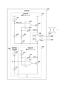
- FIG. 3 is a circuit diagram showing a configuration example of the drive circuit 200 according to the first embodiment of the present technology.
- the high voltage side voltage regulator 220 includes a current source 221, a resistor 222, an operational amplifier 223, a pMOS (p-channel Metal Oxide Semiconductor) transistor 224, a resistor 225, and a variable resistor 226.
- pMOS p-channel Metal Oxide Semiconductor
- the current source 221 and the resistor 222 are inserted in series between the power supply voltage and the node 227.
- This node 227 is connected to the low voltage side voltage regulator 240, and the low voltage VREGL is input.
- the inverting input terminal (-) of the operational amplifier 223 is connected to the connection node of the current source 221 and the resistor 222. A voltage corresponding to the low voltage VREGL is input to the inverting input terminal (-).
- the pMOS transistor 224 is inserted between the power supply voltage and the power supply terminal of the driver 250.
- the gate of the pMOS transistor 224 is connected to the output terminal of the operational amplifier 223.
- the variable resistor 226 is inserted between the non-inverting input terminal (+) of the operational amplifier 223 and the power supply terminal of the driver 250.
- the operational amplifier 223 is an example of the second operational amplifier described in the claims.
- the variable resistor 226 is an example of the third resistance described in the claims, and the resistance 225 is an example of the fourth resistance described in the claims.
- the reference voltage generation circuit 230 includes a current source 232 and a resistor 231. These current sources 232 and resistors 231 are connected in series between the power supply voltage and the ground voltage.
- the low voltage side voltage regulator 240 includes an operational amplifier 241, an nMOS (n-channel MOS) transistor 242, a resistor 243, and a variable resistor 244.
- the inverting input terminal (-) of the operational amplifier 241 is connected to the connection node of the current source 232 and the resistor 231 and the voltage of this node is input to the inverting input terminal (-) as a reference voltage.
- the nMOS transistor 242 is inserted between the ground terminal of the driver 250 and the ground voltage.
- the gate of the nMOS transistor 242 is connected to the output terminal of the operational amplifier 241.
- a power supply voltage is applied to one end of the resistor 243, and the other end is connected to the non-inverting input terminal (+) of the operational amplifier 241.
- the variable resistor 244 is inserted between the non-inverting input terminal (+) of the operational amplifier 241 and the ground terminal of the driver 250.
- the operational amplifier 241 is an example of the first operational amplifier described in the claims. Further, the variable resistor 244 is an example of the first resistance described in the claims, and the resistor 243 is an example of the second resistance described in the claims.
- the differential signal VOUT includes a positive phase signal VOUT + and a negative phase signal VOUT- with different phases.
- the driver 250 outputs one of the high voltage VREGH and the low voltage VREGL as a positive phase signal VOUT +.
- the positive phase signal VOUT + is high voltage VREGH
- the negative phase signal VOUT- is set to low voltage VREGL
- the positive phase signal VOUT + is low voltage VREGL
- the negative phase signal VOUT- is set to high voltage VREGH. ..
- the input / output of the driver 250 is a differential signal
- the input / output of the driver 250 can also be a single-ended signal.
- the reference voltage generation circuit 230 generates a reference voltage with reference to the ground voltage. For example, if the resistance value of the resistor 231 is R 1 and the value of the current from the current source 232 is I, a voltage higher than the ground voltage by I ⁇ R 1 is generated as a reference voltage.
- the low voltage side voltage regulator 240 amplifies the reference voltage by the gain G1 and outputs it as a low voltage VREGL.
- the gain G 1 is expressed by the following equation.
- G 1 R 4 / R 3 ... Equation 1
- R 4 is the resistance value of the variable resistor 244.
- R 3 is the resistance value of the resistor 243.
- the gain G 1 can be adjusted by changing the resistance value of the variable resistor 244 from the equation 1.
- the input offset administratfs 1 may occur in the operational amplifier 241 due to variations in the elements in the operational amplifier 223 and the like.
- the low voltage VREGL is expressed by the following equation.
- VREGL (IR 1 + réellefs 1 ) ⁇ G 1 ... Equation 2
- the unit of each term of the low voltage VREGL, IR 1 and the input offset whicheverfs 1 is, for example, millivolt (mV).
- the high voltage side voltage regulator 220 amplifies the voltage corresponding to the low voltage VREGL by the gain G2, and outputs the voltage as the low voltage VREGL.
- the gain G 2 is expressed by the following equation.
- G 2 R 6 / R 5 ... Equation 3
- R 6 is the resistance value of the variable resistor 226.
- R 5 is the resistance value of the resistor 225.
- the gain G 2 can be adjusted by changing the resistance value of the variable resistor 226 from the equation 3.
- the high voltage VREGH is expressed by the following equation.
- VREGH (VREGL + IR 1 + anywayfs 2 ) ⁇ G 2 ... Equation 4
- the unit of each term of the high voltage VREGH and the input offset sammlungfs 2 is, for example, millivolt (mV).
- amplitude A of the output of the driver 250 is expressed by the following equation.
- A VREGH-VREGL ⁇ ⁇ ⁇ Equation 5
- Equation 5 VREG + ⁇ VREG ⁇ ⁇ ⁇ Equation 6
- VREG G 1 (1-G 2 ) x IR 1 + G 2 x IR 2 ... Equation 7
- ⁇ VREG G 1 (1-G 2 ) ⁇ anywayfs 1 + G 2 ⁇ nostifs 2 ... Equation 8
- the VREG of the equation 6 is the amplitude when there is no input offset, and the ⁇ VREG is the variation of the amplitude caused by the input offset. These ratios are expressed by the following equations based on Equations 7 and 8.
- ⁇ VREG / VREG ⁇ G 1 (1-G 2 ) ⁇ ndfs 1 + G 2 ⁇ ndfs 2 ⁇ / ⁇ G 1 (1-G 2 ) x IR 1 + G 2 x IR 2 ⁇ ... Equation 9
- the high voltage side voltage regulator 220 refers to the low voltage VREGL and generates the high voltage VREGH from the voltage, the amplitude variation due to the offset sammlungfs 1 of the operational amplifier 241 can be reduced. Thereby, the accuracy when the control circuit 210 controls the amplitude can be improved.
- the high voltage side voltage regulator 220 and the low voltage side voltage regulator 240 use the same reference voltage.
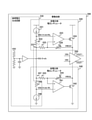
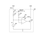
- FIG. 4 is a circuit diagram showing a configuration example of the drive circuit 200 in the comparative example.
- the input side node 227 is not connected to the low voltage side voltage regulator 240, but is connected to the reference voltage generation circuit.
- a resistance 245 and a current source 246 are further provided.
- the resistor 245 and the current source 246 are connected in series between the node 247 to which the reference voltage is supplied and the ground voltage. Further, one end of the resistor 243 is connected to the node 247 instead of the power supply voltage.
- the reference voltage generation circuit 230 of the comparative example supplies the reference voltage VREF represented by the following equation by a resistance voltage dividing circuit or an operational amplifier.
- VREF VDD / 2 + anywayfs ⁇ ⁇ ⁇ Equation 11
- VDD is the power supply voltage
- THERfs is the input offset of the operational amplifier in the reference voltage generation circuit.
- the resistance value of the resistor 245 is R 1 as in the case of the resistor 231
- the low voltage VREGL is expressed by the following equation based on the equation 11.
- VREGL VDD / 2 + Consequentlyfs- (IR 1 + réellefs 1 ) x G 1 ... Equation 12
- VREGH VDD / 2 + anywayfs + (IR 1 + réellefs 2 ) ⁇ G 2 ... Equation 13
- Equations 9 and 14 when the high voltage side voltage regulator 220 refers to the low voltage VREGL, the influence of ofs1 can be canceled out. On the other hand, in the comparative example in which the high voltage side voltage regulator 220 does not refer to the low voltage VREGL, the influence of ofs1 cannot be canceled. Therefore, in the latter case, the amplitude variation due to the offset voltage becomes larger.
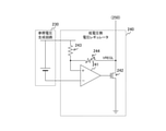
- FIG. 5 is a circuit diagram showing a configuration example of a high voltage side voltage regulator 220 having a different feedback circuit in the first embodiment of the present technology. As illustrated in the figure, a power supply voltage can also be applied to the other end of the resistor 225. With this connection, the feedback circuit on the high voltage side can be changed as compared with FIG.
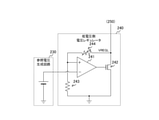
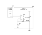
- FIG. 6 is a circuit diagram showing a configuration example of a reference voltage generation circuit 230 based on a ground voltage reference and a low voltage side voltage regulator 240 having different feedback circuits in the first embodiment of the present technology.
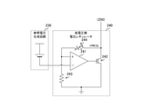
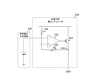
- FIG. 7 is a circuit diagram showing a configuration example of a reference voltage generation circuit 230 of the power supply voltage reference in the first embodiment of the present technology and a low voltage side voltage regulator 240 having a different feedback circuit.
- a ground voltage can be applied to the other end of the resistor 243.
- the feedback circuit on the low voltage side can be changed as compared with FIG.
- the reference voltage generation circuit 230 can generate a reference voltage with reference to the ground voltage as illustrated in FIG. 6, and generate a reference voltage with reference to the power supply voltage as illustrated with FIG. 7. You can also do it.
- the ground voltage is used as a reference, for example, a voltage higher than the ground voltage by a predetermined voltage is supplied as a reference voltage.
- the power supply voltage is used as a reference, for example, a voltage lower than the power supply voltage by a predetermined voltage is supplied as a reference voltage.
- FIG. 8 is a circuit diagram showing a configuration example of the reference voltage generation circuit 230 and the low voltage side voltage regulator 240 of the ground voltage reference in the first embodiment of the present technology.
- FIG. 9 is a circuit diagram showing a configuration example of the reference voltage generation circuit 230 and the low voltage side voltage regulator 240 of the power supply voltage reference according to the first embodiment of the present technology.
- the circuit of the low voltage side voltage regulator 240 in FIGS. 8 and 9 is the same as that illustrated in FIG.
- the reference voltage generation circuit 230 connected to the low voltage side voltage regulator 240 may be based on the ground voltage as illustrated in FIG. 8 or based on the power supply voltage as illustrated in FIG. You can also do it.
- FIG. 10 is a diagram showing an example of the waveform of the output signal in the first embodiment of the present technology and the comparative example.
- a is a diagram showing an example of the waveform of the output signal of the driver 250 in the first embodiment of the present technology.
- b is a diagram showing an example of the waveform of the output signal of the driver 250 of the comparative example in which the high voltage side voltage regulator 220 does not refer to the low voltage VREGL.
- the solid line shows the waveform of the high voltage VREGH
- the alternate long and short dash line shows the waveform of the low voltage VREGL.
- the control circuit 210 starts control at the timing T0, the high voltage VREGH and the low voltage VREGL gradually increase. Then, the difference (that is, the amplitude) between them becomes a constant value.
- the high voltage side voltage regulator 220 when the control circuit 210 starts control at the timing T0, the high voltage VREGH gradually drops. On the other hand, the low voltage VREGL gradually increases. Then, the difference (that is, the amplitude) between them becomes a constant value. As illustrated in b in the figure, in the comparative example, there is a possibility that a signal having an amplitude larger than the specified value is transmitted to the receiving side. On the other hand, as illustrated in a in the figure, in the configuration in which the high voltage side voltage regulator 220 refers to the low voltage VREGL, a signal having an amplitude larger than the specified value is not transmitted.
- the high voltage side voltage regulator 220 since the high voltage side voltage regulator 220 generates the high voltage VREGH from the low voltage VREGL, the input offset Sullivanfs 1 generated on the low voltage side can be suppressed. can. As a result, it is possible to reduce the variation in amplitude due to the input offset sammlungfs 1 and improve the accuracy when the control circuit 210 controls the amplitude.
- the high voltage side voltage regulator 220 refers to the low voltage VREGL, but in this configuration, the accuracy of amplitude control when the input offset sammlungfs 2 on the high voltage side is relatively large. May decrease.
- the drive circuit 200 of the second embodiment is different from the first embodiment in that the low voltage side voltage regulator 240 refers to the high voltage VREGH.
- FIG. 11 is a block diagram showing a configuration example of the drive circuit 200 according to the second embodiment of the present technology.
- the reference voltage generation circuit 230 supplies the reference voltage to the high voltage side voltage regulator 220.
- the high voltage side voltage regulator 220 generates a high voltage VREGH from the reference voltage and supplies it to the power supply terminal of the driver 250 and the low voltage side voltage regulator 240.
- the low voltage side voltage regulator 240 uses the high voltage VREGH as a reference voltage, generates a low voltage VREGL from the reference voltage, and supplies the low voltage VREGL to the ground terminal of the driver 250.
- the high voltage side voltage regulator 220 is an example of the first voltage regulator described in the claims. Further, the low voltage side voltage regulator 240 is an example of the second voltage regulator described in the claims.
- the high voltage side voltage regulator 220 can refer to the low voltage VREGL, and the low voltage side voltage regulator 240 can refer to the high voltage VREGH.
- FIG. 12 is a circuit diagram showing a configuration example of the reference voltage generation circuit 230 and the high voltage side voltage regulator 220 of the ground voltage reference in the second embodiment of the present technology.
- the high voltage side voltage regulator 220 of the second embodiment is different from the first embodiment in that the current source 221 and the resistor 222 are not arranged.
- the reference voltage from the reference voltage generation circuit 230 is input to the inverting input terminal (-) of the operational amplifier 223.
- the non-inverting input terminal (+) of the operational amplifier 223 is connected to the connection node of the resistor 225 and the variable resistor 226.
- One end of the resistor 225 is connected to the non-inverting input terminal (+), and a ground voltage is applied to the other end.
- FIG. 13 is a circuit diagram showing a configuration example of the reference voltage generation circuit 230 and the high voltage side voltage regulator 220 of the power supply voltage reference according to the second embodiment of the present technology.
- the reference voltage generation circuit 230 can generate a reference voltage based on the ground voltage as illustrated in FIG. 12, or can generate a reference voltage based on the power supply voltage as illustrated in FIG. can.
- FIG. 14 is a circuit diagram showing a configuration example of a reference voltage generation circuit based on a ground voltage reference and a high voltage side voltage regulator having different feedback circuits in the second embodiment of the present technology.
- FIG. 15 is a circuit diagram showing a configuration example of a reference voltage generation circuit based on a power supply voltage and a high voltage side voltage regulator having different feedback circuits in the second embodiment of the present technology.
- a power supply voltage can also be applied to the other end of the resistor 225.
- the feedback circuit of the operational amplifier 223 can be changed as compared with FIGS. 12 and 13.
- the reference voltage generation circuit 230 can generate a reference voltage based on the ground voltage as illustrated in FIG. 14, or generate a reference voltage based on the power supply voltage as illustrated in FIG. You can also do it.
- FIG. 16 is a circuit diagram showing a configuration example of the low voltage side voltage regulator 240 according to the second embodiment of the present technology.
- the low voltage side voltage regulator 240 of this second embodiment differs from the first embodiment in that a resistor 245 and a current source 246 are further arranged.
- the resistance 245 and the current source 246 are connected in series between the node 247 to which the high voltage VREGH is input and the ground voltage. Further, the inverting input terminal (-) of the operational amplifier 241 is connected to the connection node of the resistor 245 and the current source 246. The non-inverting input terminal (+) of the operational amplifier 241 is connected to the connection node of the resistor 243 and the variable resistor 244. One end of the resistor 243 is connected to the non-inverting input terminal (+) and the other end is connected to the node 247.
- FIG. 17 is a circuit diagram showing a configuration example of a low voltage side voltage regulator 240 having a different feedback circuit in the second embodiment of the present technology. As illustrated in the figure, a ground voltage can be applied to the other end of the resistor 243.
- the low voltage side voltage regulator 240 since the low voltage side voltage regulator 240 generates the low voltage VREGL from the high voltage VREGH, the input offset obviouslyfs 2 generated on the high voltage side can be suppressed. can. As a result, the variation in amplitude due to the input offset sammlungfs 2 can be reduced, and the accuracy when the control circuit 210 controls the amplitude can be improved.
- the technology according to the present disclosure can be applied to various products.
- the technology according to the present disclosure is realized as a device mounted on a moving body of any kind such as an automobile, an electric vehicle, a hybrid electric vehicle, a motorcycle, a bicycle, a personal mobility, an airplane, a drone, a ship, and a robot. You may.
- FIG. 18 is a block diagram showing a schematic configuration example of a vehicle control system, which is an example of a mobile control system to which the technique according to the present disclosure can be applied.
- the vehicle control system 12000 includes a plurality of electronic control units connected via the communication network 12001.
- the vehicle control system 12000 includes a drive system control unit 12010, a body system control unit 12020, an outside information detection unit 12030, an in-vehicle information detection unit 12040, and an integrated control unit 12050.
- a microcomputer 12051, an audio image output unit 12052, and an in-vehicle network I / F (interface) 12053 are shown as a functional configuration of the integrated control unit 12050.
- the drive system control unit 12010 controls the operation of the device related to the drive system of the vehicle according to various programs.
- the drive system control unit 12010 has a driving force generator for generating the driving force of the vehicle such as an internal combustion engine or a driving motor, a driving force transmission mechanism for transmitting the driving force to the wheels, and a steering angle of the vehicle. It functions as a control device such as a steering mechanism for adjusting and a braking device for generating braking force of the vehicle.
- the body system control unit 12020 controls the operation of various devices mounted on the vehicle body according to various programs.
- the body system control unit 12020 functions as a keyless entry system, a smart key system, a power window device, or a control device for various lamps such as headlamps, back lamps, brake lamps, turn signals or fog lamps.
- the body system control unit 12020 may be input with radio waves transmitted from a portable device that substitutes for the key or signals of various switches.
- the body system control unit 12020 receives inputs of these radio waves or signals and controls a vehicle door lock device, a power window device, a lamp, and the like.
- the vehicle outside information detection unit 12030 detects information outside the vehicle equipped with the vehicle control system 12000.
- the image pickup unit 12031 is connected to the vehicle outside information detection unit 12030.
- the vehicle outside information detection unit 12030 causes the image pickup unit 12031 to capture an image of the outside of the vehicle and receives the captured image.
- the vehicle outside information detection unit 12030 may perform object detection processing or distance detection processing such as a person, a vehicle, an obstacle, a sign, or a character on the road surface based on the received image.
- the image pickup unit 12031 is an optical sensor that receives light and outputs an electric signal according to the amount of the light received.
- the image pickup unit 12031 can output an electric signal as an image or can output it as distance measurement information. Further, the light received by the image pickup unit 12031 may be visible light or invisible light such as infrared light.
- the in-vehicle information detection unit 12040 detects the in-vehicle information.
- a driver state detection unit 12041 that detects a driver's state is connected to the vehicle interior information detection unit 12040.
- the driver state detection unit 12041 includes, for example, a camera that images the driver, and the in-vehicle information detection unit 12040 determines the degree of fatigue or concentration of the driver based on the detection information input from the driver state detection unit 12041. It may be calculated, or it may be determined whether the driver has fallen asleep.
- the microcomputer 12051 calculates the control target value of the driving force generator, the steering mechanism, or the braking device based on the information inside and outside the vehicle acquired by the vehicle exterior information detection unit 12030 or the vehicle interior information detection unit 12040, and the drive system control unit.
- a control command can be output to 12010.
- the microcomputer 12051 realizes ADAS (Advanced Driver Assistance System) functions including vehicle collision avoidance or impact mitigation, follow-up driving based on inter-vehicle distance, vehicle speed maintenance driving, vehicle collision warning, vehicle lane deviation warning, and the like. It is possible to perform cooperative control for the purpose of.
- ADAS Advanced Driver Assistance System
- the microcomputer 12051 controls the driving force generating device, the steering mechanism, the braking device, and the like based on the information around the vehicle acquired by the vehicle exterior information detection unit 12030 or the vehicle interior information detection unit 12040. It is possible to perform coordinated control for the purpose of automatic driving that runs autonomously without depending on the operation.
- the microcomputer 12051 can output a control command to the body system control unit 12020 based on the information outside the vehicle acquired by the vehicle outside information detection unit 12030.
- the microcomputer 12051 controls the headlamps according to the position of the preceding vehicle or the oncoming vehicle detected by the outside information detection unit 12030, and performs cooperative control for the purpose of anti-glare such as switching the high beam to the low beam. It can be carried out.
- the audio image output unit 12052 transmits an output signal of at least one of audio and image to an output device capable of visually or audibly notifying information to the passenger or the outside of the vehicle.
- an audio speaker 12061, a display unit 12062, and an instrument panel 12063 are exemplified as output devices.
- the display unit 12062 may include, for example, at least one of an onboard display and a head-up display.
- FIG. 19 is a diagram showing an example of the installation position of the imaging unit 12031.
- the imaging unit 12031 As the imaging unit 12031, the imaging unit 12101, 12102, 12103, 12104, 12105 is provided.
- the image pickup units 12101, 12102, 12103, 12104, 12105 are provided, for example, at positions such as the front nose, side mirrors, rear bumpers, back doors, and the upper part of the windshield in the vehicle interior of the vehicle 12100.
- the image pickup unit 12101 provided on the front nose and the image pickup section 12105 provided on the upper part of the windshield in the vehicle interior mainly acquire an image in front of the vehicle 12100.
- the image pickup units 12102 and 12103 provided in the side mirror mainly acquire images of the side of the vehicle 12100.
- the image pickup unit 12104 provided in the rear bumper or the back door mainly acquires an image of the rear of the vehicle 12100.
- the image pickup unit 12105 provided on the upper part of the windshield in the vehicle interior is mainly used for detecting a preceding vehicle, a pedestrian, an obstacle, a traffic light, a traffic sign, a lane, or the like.
- FIG. 19 shows an example of the photographing range of the imaging units 12101 to 12104.
- the imaging range 12111 indicates the imaging range of the imaging unit 12101 provided on the front nose
- the imaging ranges 12112 and 12113 indicate the imaging range of the imaging units 12102 and 12103 provided on the side mirrors, respectively
- the imaging range 12114 indicates the imaging range.
- the imaging range of the imaging unit 12104 provided on the rear bumper or the back door is shown. For example, by superimposing the image data captured by the imaging units 12101 to 12104, a bird's-eye view image of the vehicle 12100 can be obtained. $
- At least one of the image pickup units 12101 to 12104 may have a function of acquiring distance information.
- at least one of the image pickup units 12101 to 12104 may be a stereo camera including a plurality of image pickup elements, or may be an image pickup element having pixels for phase difference detection.
- the microcomputer 12051 has a distance to each three-dimensional object within the image pickup range 12111 to 12114 based on the distance information obtained from the image pickup unit 12101 to 12104, and a temporal change of this distance (relative speed with respect to the vehicle 12100). By obtaining can. Further, the microcomputer 12051 can set an inter-vehicle distance to be secured in advance in front of the preceding vehicle, and can perform automatic braking control (including follow-up stop control), automatic acceleration control (including follow-up start control), and the like. In this way, it is possible to perform coordinated control for the purpose of automatic driving or the like in which the vehicle travels autonomously without depending on the operation of the driver.
- automatic braking control including follow-up stop control
- automatic acceleration control including follow-up start control
- the microcomputer 12051 converts three-dimensional object data related to a three-dimensional object into two-wheeled vehicles, ordinary vehicles, large vehicles, pedestrians, electric poles, and other three-dimensional objects based on the distance information obtained from the image pickup units 12101 to 12104. It can be classified and extracted and used for automatic avoidance of obstacles. For example, the microcomputer 12051 distinguishes obstacles around the vehicle 12100 into obstacles that are visible to the driver of the vehicle 12100 and obstacles that are difficult to see. Then, the microcomputer 12051 determines the collision risk indicating the risk of collision with each obstacle, and when the collision risk is equal to or higher than the set value and there is a possibility of collision, the microcomputer 12051 via the audio speaker 12061 or the display unit 12062. By outputting an alarm to the driver and performing forced deceleration and avoidance steering via the drive system control unit 12010, driving support for collision avoidance can be provided.
- At least one of the image pickup units 12101 to 12104 may be an infrared camera that detects infrared rays.
- the microcomputer 12051 can recognize a pedestrian by determining whether or not a pedestrian is present in the captured image of the imaging unit 12101 to 12104.
- pedestrian recognition is, for example, a procedure for extracting feature points in an image captured by an image pickup unit 12101 to 12104 as an infrared camera, and pattern matching processing is performed on a series of feature points indicating the outline of an object to determine whether or not the pedestrian is a pedestrian. It is done by the procedure to determine.
- the audio image output unit 12052 determines the square contour line for emphasizing the recognized pedestrian.
- the display unit 12062 is controlled so as to superimpose and display. Further, the audio image output unit 12052 may control the display unit 12062 so as to display an icon or the like indicating a pedestrian at a desired position.
- the above is an example of a vehicle control system to which the technology according to the present disclosure can be applied.
- the technique according to the present disclosure can be applied to the imaging unit 12031 among the configurations described above.
- the transmission circuit 100 of FIG. 1 can be applied to the communication interface of the image pickup unit 12031.
- the signal quality can be improved by improving the amplitude control accuracy.
- the present technology can have the following configurations.
- a first voltage regulator that generates one of a pair of voltages from a predetermined reference voltage and supplies it to one of the power supply terminal and the ground terminal of the driver.
- a control circuit comprising a second voltage regulator that generates the other of the pair of voltages from one of the pair of voltages and supplies it to the other of the power supply terminal and the ground terminal.
- the first voltage regulator produces the lower of the pair of voltages.
- the control circuit according to (1) above, wherein the second voltage regulator generates the higher of the pair of voltages.
- the first voltage regulator produces the higher of the pair of voltages.
- the control circuit according to (1) above, wherein the second voltage regulator generates the lower of the pair of voltages.
- a reference voltage generation circuit that generates the reference voltage and supplies the reference voltage to the first voltage regulator.
- the first voltage regulator is A first operational amplifier that outputs one of the pair of voltages, A first resistor inserted between one of the pair of input terminals of the first operational amplifier and one of the power supply terminal and the ground terminal, A second resistor having one end connected to one of the pair of input terminals is provided.
- the control circuit according to any one of (1) to (6), wherein the reference voltage is input to the other of the pair of input terminals.
- the second voltage regulator is A second operational amplifier that outputs the other of the pair of voltages, A third resistor inserted between one of the pair of input terminals of the second operational amplifier and the other of the power supply terminal and the ground terminal, A fourth resistor having one end connected to one of the pair of input terminals is provided.
- the control circuit according to (7) wherein a voltage corresponding to one of the pair of voltages is applied to the other of the pair of input terminals.
- (11) The control circuit according to (10), wherein one of the pair of voltages is applied to the other end of the fourth resistance.
- (12) The control circuit according to (10) above, wherein a predetermined power supply voltage is applied to the other end of the fourth resistance.
- (123) With the driver A first voltage regulator that generates one of a pair of voltages from a predetermined reference voltage and supplies it to one of the power supply terminal and the ground terminal of the driver.
- a drive circuit comprising a second voltage regulator that generates the other of the pair of voltages from one of the pair of voltages and supplies it to the other of the power supply terminal and the ground terminal.
- Transmission circuit 110 Transmission signal generator 200 Drive circuit 210 Control circuit 220 High voltage side voltage regulator 221 232, 246 Current source 222, 225, 231, 243, 245 Resistance 223, 241 Operational amplifier 224 pMOS transistor 226, 244 Variable resistance 230 Reference voltage generation circuit 240 Low voltage side voltage regulator 242 nMOS transistor 250 Driver 300 Reception circuit 12031 Image pickup unit
Landscapes
- Engineering & Computer Science (AREA)
- Computer Hardware Design (AREA)
- Physics & Mathematics (AREA)
- Computing Systems (AREA)
- General Engineering & Computer Science (AREA)
- Mathematical Physics (AREA)
- Electromagnetism (AREA)
- General Physics & Mathematics (AREA)
- Radar, Positioning & Navigation (AREA)
- Automation & Control Theory (AREA)
- Continuous-Control Power Sources That Use Transistors (AREA)
- Amplifiers (AREA)
Abstract
電圧レギュレータにより振幅を制御する制御回路において、振幅を高精度で制御する。 制御回路は、第1の電圧レギュレータと、第2の電圧レギュレータとを具備する。この制御回路内の第1の電圧レギュレータは、所定の参照電圧から一対の電圧の一方を生成してドライバの電源端子および接地端子の一方に供給する。また、第2の電圧レギュレータは、一対の電圧の一方から一対の電圧の他方を生成して電源端子および接地端子の他方に供給する。
Description
本技術は、制御回路に関する。詳しくは、電圧レギュレータを用いる制御回路および駆動回路に関する。
従来より、通信インターフェースの送信側の駆動回路においては、ドライバに加えて、そのドライバの振幅を制御するために電圧レギュレータが配置されることが多い。例えば、ドライバとともに電源側と接地側とのそれぞれに電圧レギュレータを設けた駆動回路が提案されている(例えば、特許文献1参照。)。この駆動回路内の電源側の電圧レギュレータは所定の参照電圧からドライバの出力のハイレベルを生成し、接地側の電圧レギュレータはその参照電圧からドライバの出力のローレベルを生成する。
上述の従来技術では、電源側および接地側の両方に電圧レギュレータを配置することにより、PSRR(Power Supply Rejection Ratio)の向上を図っている。しかしながら、上述の駆動回路では、電圧レギュレータ内のオペアンプの入力オフセットにより、ドライバの出力信号の振幅にばらつきが生じることがある。このばらつきにより、電圧レギュレータが振幅を制御する際の精度が低下するおそれがある。
本技術はこのような状況に鑑みて生み出されたものであり、電圧レギュレータにより振幅を制御する制御回路において、振幅制御の精度を向上させることを目的とする。
本技術は、上述の問題点を解消するためになされたものであり、その第1の側面は、所定の参照電圧から一対の電圧の一方を生成してドライバの電源端子および接地端子の一方に供給する第1の電圧レギュレータと、上記一対の電圧の一方から上記一対の電圧の他方を生成して上記電源端子および上記接地端子の他方に供給する第2の電圧レギュレータとを具備する制御回路である。これにより、振幅が高精度で制御されるという作用をもたらす。
また、この第1の側面において、上記第1の電圧レギュレータは、上記一対の電圧のうち低い方を生成し、上記第2の電圧レギュレータは、上記一対の電圧のうち高い方を生成してもよい。これにより、低電圧から高電圧が生成されるという作用をもたらす。
また、この第1の側面において、上記第1の電圧レギュレータは、上記一対の電圧のうち高い方を生成し、上記第2の電圧レギュレータは、上記一対の電圧のうち低い方を生成してもよい。これにより、高電圧から低電圧が生成されるという作用をもたらす。
また、この第1の側面において、上記参照電圧を生成して上記第1の電圧レギュレータに供給する参照電圧生成回路をさらに具備してもよい。これにより、参照電圧が第1の電圧レギュレータに入力されるという作用をもたらす。
また、この第1の側面において、上記参照電圧生成回路は、所定の接地電圧を基準として上記参照電圧を生成してもよい。これにより、接地電圧基準の参照電圧が生成されるという作用をもたらす。
また、この第1の側面において、上記参照電圧生成回路は、所定の電源電圧を基準として上記参照電圧を生成してもよい。これにより、電源電圧基準の参照電圧が生成されるという作用をもたらす。
また、この第1の側面において、上記第1の電圧レギュレータは、上記一対の電圧の一方を出力する第1オペアンプと、上記第1オペアンプの一対の入力端子の一方と上記電源端子および上記接地端子の一方との間に挿入された第1抵抗と、上記一対の入力端子の一方に一端が接続された第2抵抗とを備え、上記一対の入力端子の他方には、上記参照電圧が入力されてもよい。これにより、参照電圧が増幅されるという作用をもたらす。
また、この第1の側面において、上記第2抵抗の他端には、所定の接地電圧が印加されてもよい。これにより、フィードバック回路が形成されるという作用をもたらす。
また、この第1の側面において、上記第2抵抗の他端には、所定の電源電圧が印加されてもよい。これにより、フィードバック回路が形成されるという作用をもたらす。
また、この第1の側面において、上記第2の電圧レギュレータは、上記一対の電圧の他方を出力する第2オペアンプと、上記第2オペアンプの一対の入力端子の一方と上記電源端子および上記接地端子の他方との間に挿入された第3抵抗と、上記一対の入力端子の一方に一端が接続された第4抵抗とを備え、上記一対の入力端子の他方には、上記一対の電圧の一方に応じた電圧が印加されてもよい。これにより、一対の電圧の一方が増幅されるという作用をもたらす。
また、この第1の側面において、上記第4抵抗の他端には、上記一対の電圧の一方が印加されてもよい。これにより、フィードバック回路が形成されるという作用をもたらす。
また、この第1の側面において、上記第4抵抗の他端には、所定の電源電圧が印加されてもよい。これにより、フィードバック回路が形成されるという作用をもたらす。
また、本技術の第2の側面は、ドライバと、所定の参照電圧から一対の電圧の一方を生成して上記ドライバの電源端子および接地端子の一方に供給する第1の電圧レギュレータと、上記一対の電圧の一方から上記一対の電圧の他方を生成して上記電源端子および上記接地端子の他方に供給する第2の電圧レギュレータとを具備する駆動回路である。これにより、高精度で振幅が制御された信号が出力されるという作用をもたらす。
以下、本技術を実施するための形態(以下、実施の形態と称する)について説明する。説明は以下の順序により行う。
1.第1の実施の形態(高電圧側電圧レギュレータが低電圧から高電圧を生成する例)
2.第2の実施の形態(低電圧側電圧レギュレータが高電圧から低電圧を生成する例)
3.移動体への応用例
1.第1の実施の形態(高電圧側電圧レギュレータが低電圧から高電圧を生成する例)
2.第2の実施の形態(低電圧側電圧レギュレータが高電圧から低電圧を生成する例)
3.移動体への応用例
<1.第1の実施の形態>
[インターフェース回路の構成例]
図1は、本技術の実施の形態におけるインターフェース回路の一構成例を示すブロック図である。このインターフェース回路は、信号を伝送するための回路であり、送信回路100および受信回路300を備える。
[インターフェース回路の構成例]
図1は、本技術の実施の形態におけるインターフェース回路の一構成例を示すブロック図である。このインターフェース回路は、信号を伝送するための回路であり、送信回路100および受信回路300を備える。
送信回路100は、信号を送信する回路であり、送信信号生成部110および駆動回路200を備える。
送信信号生成部110は、送信すべき信号を生成するものである。この送信信号生成部110は、例えば、差動信号を生成し、信号線119を介して駆動回路200に供給する。
駆動回路200は、送信信号生成部110からの差動信号を増幅し、伝送路209へ出力するものである。受信回路300は、駆動回路200からの差動信号を、レシーバなどにより受信するものである。
[駆動回路の構成例]
図2は、本技術の第1の実施の形態における駆動回路200の一構成例を示すブロック図である。この駆動回路200は、制御回路210およびドライバ250を備える。
図2は、本技術の第1の実施の形態における駆動回路200の一構成例を示すブロック図である。この駆動回路200は、制御回路210およびドライバ250を備える。
制御回路210は、ドライバ250の出力信号の振幅を制御するものである。この制御回路210は、高電圧側電圧レギュレータ220、参照電圧生成回路230および低電圧側電圧レギュレータ240を備える。
ドライバ250は、送信信号生成部110からの差動信号VINの振幅を調整し、差動信号VOUTとして受信回路300に出力するものである。このドライバ250の電源端子には、高電圧VREGHが入力される。また、ドライバ250の接地端子には、高電圧VREGHより低い低電圧VREGLが入力される。なお、高電圧VREGHおよび低電圧VREGLは、特許請求の範囲に記載の一対の電圧の一例である。
参照電圧生成回路230は、所定の参照電圧を生成して低電圧側電圧レギュレータ240に供給するものである。
低電圧側電圧レギュレータ240は、参照電圧から低電圧VREGLを生成し、ドライバ250の接地端子と高電圧側電圧レギュレータ220とに供給するものである。なお、低電圧側電圧レギュレータ240は、特許請求の範囲に記載の第1の電圧レギュレータの一例である。
高電圧側電圧レギュレータ220は、低電圧VREGLを参照電圧として、その参照電圧から高電圧VREGHを生成し、ドライバ250の電源端子に供給するものである。なお、高電圧側電圧レギュレータ220は、特許請求の範囲に記載の第2の電圧レギュレータの一例である。
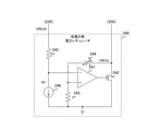
図3は、本技術の第1の実施の形態における駆動回路200の一構成例を示す回路図である。この高電圧側電圧レギュレータ220は、電流源221、抵抗222、オペアンプ223、pMOS(p-channel Metal Oxide Semiconductor)トランジスタ224、抵抗225および可変抵抗226を備える。
電流源221および抵抗222は、電源電圧とノード227との間に直列に挿入される。このノード227は、低電圧側電圧レギュレータ240と接続され、低電圧VREGLが入力される。
オペアンプ223の反転入力端子(-)は、電流源221および抵抗222の接続ノードに接続される。この反転入力端子(-)には、低電圧VREGLに応じた電圧が入力される。
pMOSトランジスタ224は、電源電圧とドライバ250の電源端子との間に挿入される。このpMOSトランジスタ224のゲートは、オペアンプ223の出力端子に接続される。
抵抗225の一端は、オペアンプ223の非反転入力端子(+)に接続され、他端はノード227に接続される。可変抵抗226は、オペアンプ223の非反転入力端子(+)と、ドライバ250の電源端子との間に挿入される。なお、オペアンプ223は、特許請求の範囲に記載の第2オペアンプの一例である。また、可変抵抗226は、特許請求の範囲に記載の第3抵抗の一例であり、抵抗225は、特許請求の範囲に記載の第4抵抗の一例である。
参照電圧生成回路230は、電流源232および抵抗231を備える。これらの電流源232および抵抗231は、電源電圧と接地電圧との間において直列に接続される。
また、低電圧側電圧レギュレータ240は、オペアンプ241、nMOS(n-channel MOS)トランジスタ242、抵抗243および可変抵抗244を備える。
オペアンプ241の反転入力端子(-)は、電流源232および抵抗231の接続ノードに接続され、このノードの電圧が参照電圧として反転入力端子(-)に入力される。
nMOSトランジスタ242は、ドライバ250の接地端子と接地電圧との間に挿入される。このnMOSトランジスタ242のゲートは、オペアンプ241の出力端子に接続される。
抵抗243の一端には、電源電圧が印加され、他端は、オペアンプ241の非反転入力端子(+)に接続される。可変抵抗244は、オペアンプ241の非反転入力端子(+)と、ドライバ250の接地端子との間に挿入される。なお、オペアンプ241は、特許請求の範囲に記載の第1オペアンプの一例である。また、可変抵抗244は、特許請求の範囲に記載の第1抵抗の一例であり、抵抗243は、特許請求の範囲に記載の第2抵抗の一例である。
また、差動信号VOUTは、位相が互いに異なる正相信号VOUT+および逆相信号VOUT-を含む。ドライバ250は、高電圧VREGHおよび低電圧VREGLの一方を正相信号VOUT+として出力する。正相信号VOUT+が高電圧VREGHのときは、逆相信号VOUT-は低電圧VREGLに設定され、正相信号VOUT+が低電圧VREGLのときは、逆相信号VOUT-は高電圧VREGHに設定される。
なお、ドライバ250の入出力を差動信号としているが、ドライバ250の入出力をシングルエンド信号とすることもできる。
同図に例示した回路構成により、参照電圧生成回路230は、接地電圧を基準として参照電圧を生成する。例えば、抵抗231の抵抗値をR1とし、電流源232からの電流の値をIとすると、接地電圧よりI×R1だけ高い電圧が参照電圧として生成される。
また、低電圧側電圧レギュレータ240は、参照電圧をゲインG1により増幅し、低電圧VREGLとして出力する。ここで、ゲインG1は、次の式により表される。
G1=R4/R3 ・・・式1
上式において、R4は、可変抵抗244の抵抗値である。R3は、抵抗243の抵抗値である。
G1=R4/R3 ・・・式1
上式において、R4は、可変抵抗244の抵抗値である。R3は、抵抗243の抵抗値である。
ゲインG1は、式1より、可変抵抗244の抵抗値を変更することによって調整することができる。
ここで、オペアンプ241には、オペアンプ223内の素子のばらつきなどに起因して、入力オフセットоfs1が生じることがある。この入力オフセットоfs1を考慮すると、低電圧VREGLは、次の式により表される。
VREGL=(IR1+оfs1)×G1 ・・・式2
上式において、低電圧VREGL、IR1および入力オフセットоfs1の各項の単位は、例えば、ミリボルト(mV)である。
VREGL=(IR1+оfs1)×G1 ・・・式2
上式において、低電圧VREGL、IR1および入力オフセットоfs1の各項の単位は、例えば、ミリボルト(mV)である。
また、高電圧側電圧レギュレータ220は、低電圧VREGLに応じた電圧をゲインG2により増幅し、低電圧VREGLとして出力する。ここで、ゲインG2は、次の式により表される。
G2=R6/R5 ・・・式3
上式において、R6は、可変抵抗226の抵抗値である。R5は、抵抗225の抵抗値である。
G2=R6/R5 ・・・式3
上式において、R6は、可変抵抗226の抵抗値である。R5は、抵抗225の抵抗値である。
ゲインG2は、式3より、可変抵抗226の抵抗値を変更することによって調整することができる。
オペアンプ223の入力オフセットоfs2を考慮すると、高電圧VREGHは、次の式により表される。
VREGH=(VREGL+IR1+оfs2)×G2 ・・・式4
上式において、高電圧VREGHおよび入力オフセットоfs2の各項の単位は、例えば、ミリボルト(mV)である。
上式において、高電圧VREGHおよび入力オフセットоfs2の各項の単位は、例えば、ミリボルト(mV)である。
また、ドライバ250の出力の振幅Aは、次の式により表される。
A=VREGH-VREGL ・・・式5
A=VREGH-VREGL ・・・式5
式5に式2および式4を代入して変形すると、次の式が得られる。
A=VREG+ΔVREG ・・・式6
VREG=G1(1-G2)×IR1+G2×IR2 ・・・式7
ΔVREG=G1(1-G2)×оfs1+G2×оfs2 …式8
A=VREG+ΔVREG ・・・式6
VREG=G1(1-G2)×IR1+G2×IR2 ・・・式7
ΔVREG=G1(1-G2)×оfs1+G2×оfs2 …式8
式6のVREGは、入力オフセットの無い場合の振幅であり、ΔVREGは、入力オフセットにより生じる振幅のばらつきである。これらの比率は、式7および式8に基づいて次の式により表される。
ΔVREG/VREG={G1(1-G2)×оfs1+G2×оfs2}/
{G1(1-G2)×IR1+G2×IR2}…式9
ΔVREG/VREG={G1(1-G2)×оfs1+G2×оfs2}/
{G1(1-G2)×IR1+G2×IR2}…式9
ここで、ゲインG2を「1」とすると、式9より次の式が得られる。
ΔVREG/VREG=оfs2/IR2 ・・・式10
ΔVREG/VREG=оfs2/IR2 ・・・式10
例えば、VREGを450ミリボルト(mV)とし、入力オフセットоfs2を5ミリボルト(mV)とすると、式10より、振幅は1.1%程度ばらつく。なお、ゲインG2が「1」以外である場合は入力オフセットоfs1の項が残るが、その場合であっても、入力オフセットоfs2と比較して入力オフセットоfs1の影響は少ない。
式10より、高電圧側電圧レギュレータ220が低電圧VREGLを参照して、その電圧から高電圧VREGHを生成する構成を用いれば、オペアンプ241のオフセットоfs1による振幅のばらつきを低減することができる。これにより、制御回路210が振幅を制御する際の精度を向上させることができる。
ここで、比較例として高電圧側電圧レギュレータ220および低電圧側電圧レギュレータ240が同一の参照電圧を用いる構成を想定する。
図4は、比較例における駆動回路200の一構成例を示す回路図である。比較例の高電圧側電圧レギュレータ220において、入力側のノード227は、低電圧側電圧レギュレータ240には接続されず、参照電圧生成回路に接続される。
また、比較例の低電圧側電圧レギュレータ240において、抵抗245および電流源246がさらに設けられる。抵抗245および電流源246は、参照電圧が供給されるノード247と、接地電圧との間において直列に接続される。また、抵抗243の一端は、電源電圧でなく、ノード247に接続される。
比較例の参照電圧生成回路230は、抵抗分圧回路やオペアンプにより、次の式で表される参照電圧VREFを供給する。
VREF=VDD/2+оfs ・・・式11
上式において、VDDは、電源電圧であり、оfsは、参照電圧生成回路内のオペアンプの入力オフセットである。抵抗245の抵抗値を抵抗231と同様にR1とすると、式11に基づいて低電圧VREGLは、次の式により表される。
VREGL=VDD/2+оfs-(IR1+оfs1)×G1…式12
VREF=VDD/2+оfs ・・・式11
上式において、VDDは、電源電圧であり、оfsは、参照電圧生成回路内のオペアンプの入力オフセットである。抵抗245の抵抗値を抵抗231と同様にR1とすると、式11に基づいて低電圧VREGLは、次の式により表される。
VREGL=VDD/2+оfs-(IR1+оfs1)×G1…式12
また、式11に基づいて高電圧VREGHは、次の式により表される。
VREGH=VDD/2+оfs+(IR1+оfs2)×G2…式13
VREGH=VDD/2+оfs+(IR1+оfs2)×G2…式13
式12および式13より、次の式が得られる。
ΔVREG/VREG=(G1×оfs1+G2×оfs2)/
(G1×IR1+G2×IR2) ・・・式14
ΔVREG/VREG=(G1×оfs1+G2×оfs2)/
(G1×IR1+G2×IR2) ・・・式14
ゲインG1およびG2を「1」し、VREGを450ミリボルト(mV)とし、入力オフセットоfs1およびоfs2を5ミリボルト(mV)とすると、式14より、振幅は2.2%程度ばらつく。
式9および式14に例示したように、高電圧側電圧レギュレータ220が低電圧VREGLを参照する場合では、ofs1の影響を打ち消すことが出来る。それに対し、高電圧側電圧レギュレータ220が低電圧VREGLを参照しない比較例ではofs1の影響を打ち消すことが出来ない。したがって、後者の方がオフセット電圧による振幅のばらつきが大きくなる。
図5は、本技術の第1の実施の形態における、フィードバック回路の異なる高電圧側電圧レギュレータ220の一構成例を示す回路図である。同図に例示するように、抵抗225の他端に電源電圧を印加することもできる。この接続により、図3と比較して、高電圧側のフィードバック回路を変えることができる。
図6は、本技術の第1の実施の形態における接地電圧基準の参照電圧生成回路230とフィードバック回路の異なる低電圧側電圧レギュレータ240との一構成例を示す回路図である。
図7は、本技術の第1の実施の形態における電源電圧基準の参照電圧生成回路230とフィードバック回路の異なる低電圧側電圧レギュレータ240との一構成例を示す回路図である。
図6および図7に例示するように、抵抗243の他端に接地電圧を印加することもできる。この接続により、図3と比較して低電圧側のフィードバック回路を変えることができる。
また、参照電圧生成回路230は、図6に例示するように、接地電圧を基準として参照電圧を生成することもできるし、図7に例示するように、電源電圧を基準として参照電圧を生成することもできる。接地電圧を基準とする場合、例えば、接地電圧より、所定電圧だけ高い電圧が参照電圧として供給される。電源電圧を基準とする場合、例えば、電源電圧より、所定電圧だけ低い電圧が参照電圧として供給される。
図8は、本技術の第1の実施の形態における接地電圧基準の参照電圧生成回路230と低電圧側電圧レギュレータ240との一構成例を示す回路図である。
図9は、本技術の第1の実施の形態における電源電圧基準の参照電圧生成回路230と低電圧側電圧レギュレータ240との一構成例を示す回路図である。
図8および図9の低電圧側電圧レギュレータ240の回路は、図3に例示したものと同様である。この低電圧側電圧レギュレータ240に接続される参照電圧生成回路230は、図8に例示するように、接地電圧を基準とすることもできるし、図9に例示するように、電源電圧を基準とすることもできる。
図10は、本技術の第1の実施の形態と比較例とにおける出力信号の波形の一例を示す図である。同図におけるaは、本技術の第1の実施の形態におけるドライバ250の出力信号の波形の一例を示す図である。同図におけるbは、高電圧側電圧レギュレータ220が低電圧VREGLを参照しない比較例のドライバ250の出力信号の波形の一例を示す図である。同図において、実線は、高電圧VREGHの波形を示し、一点鎖線は、低電圧VREGLの波形を示す。
同図におけるaに例示するように、高電圧側電圧レギュレータ220が低電圧VREGLを参照する場合、タイミングT0で制御回路210が制御を開始すると、高電圧VREGHおよび低電圧VREGLが徐々に上昇する。そして、それらの差分(すなわち、振幅)は、一定の値となる。
また、同図におけるbに例示するように、高電圧側電圧レギュレータ220が低電圧VREGLを参照しない比較例では、タイミングT0で制御回路210が制御を開始すると、高電圧VREGHが徐々に降下する。一方、低電圧VREGLは徐々に上昇する。そして、それらの差分(すなわち、振幅)は、一定の値となる。同図におけるbに例示するように、比較例では、規定値よりも大きな振幅の信号が受信側へ送信されるおそれがある。一方、同図におけるaに例示したように、高電圧側電圧レギュレータ220が低電圧VREGLを参照する構成では、規定値よりも大きな振幅の信号が送信されることは無い。
このように、本技術の第1の実施の形態によれば、高電圧側電圧レギュレータ220が低電圧VREGLから高電圧VREGHを生成するため、低電圧側で生じる入力オフセットоfs1を抑制することができる。これにより、その入力オフセットоfs1による振幅のばらつきを低減し、制御回路210が振幅を制御する際の精度を向上させることができる。
<2.第2の実施の形態>
上述の第1の実施の形態では、高電圧側電圧レギュレータ220が低電圧VREGLを参照していたが、この構成では、高電圧側の入力オフセットоfs2が比較的大きい場合に振幅の制御の精度が低下するおそれがある。この第2の実施の形態の駆動回路200は、低電圧側電圧レギュレータ240が高電圧VREGHを参照する点において第1の実施の形態と異なる。
上述の第1の実施の形態では、高電圧側電圧レギュレータ220が低電圧VREGLを参照していたが、この構成では、高電圧側の入力オフセットоfs2が比較的大きい場合に振幅の制御の精度が低下するおそれがある。この第2の実施の形態の駆動回路200は、低電圧側電圧レギュレータ240が高電圧VREGHを参照する点において第1の実施の形態と異なる。
図11は、本技術の第2の実施の形態における駆動回路200の一構成例を示すブロック図である。この第2の実施の形態の駆動回路200において、参照電圧生成回路230は、参照電圧を高電圧側電圧レギュレータ220に供給する。高電圧側電圧レギュレータ220は、参照電圧から高電圧VREGHを生成し、ドライバ250の電源端子と低電圧側電圧レギュレータ240とに供給する。また、低電圧側電圧レギュレータ240は、高電圧VREGHを参照電圧として、その参照電圧から低電圧VREGLを生成し、ドライバ250の接地端子に供給する。
同図の構成では、式10の代わりに、次の式が得られる。
ΔVREG/VREG=оfs1/IR1 ・・・式15
ΔVREG/VREG=оfs1/IR1 ・・・式15
なお、高電圧側電圧レギュレータ220は、特許請求の範囲に記載の第1の電圧レギュレータの一例である。また、低電圧側電圧レギュレータ240は、特許請求の範囲に記載の第2の電圧レギュレータの一例である。
図2および図11に例示したように、高電圧側電圧レギュレータ220が低電圧VREGLを参照することもできるし、低電圧側電圧レギュレータ240が高電圧VREGHを参照することもできる。
式10および式15より、低電圧側の入力オフセットоfs1が比較的大きい場合は、図2の構成を用いることが望ましい。一方、高電圧側の入力オフセットоfs2が比較的大きい場合には、図11の構成を用いることが望ましい。
図12は、本技術の第2の実施の形態における接地電圧基準の参照電圧生成回路230と高電圧側電圧レギュレータ220との一構成例を示す回路図である。この第2の実施の形態の高電圧側電圧レギュレータ220は、電流源221および抵抗222が配置されない点において第1の実施の形態と異なる。また、オペアンプ223の反転入力端子(-)には、参照電圧生成回路230からの参照電圧が入力される。オペアンプ223の非反転入力端子(+)は、抵抗225および可変抵抗226の接続ノードに接続される。抵抗225の一端は、非反転入力端子(+)に接続され、他端には接地電圧が印加される。
図13は、本技術の第2の実施の形態における電源電圧基準の参照電圧生成回路230と高電圧側電圧レギュレータ220との一構成例を示す回路図である。
参照電圧生成回路230は、図12に例示するように、接地電圧を基準として参照電圧を生成することもできるし、図13に例示するように、電源電圧を基準として参照電圧を生成することもできる。
図14は、本技術の第2の実施の形態における接地電圧基準の参照電圧生成回路とフィードバック回路の異なる高電圧側電圧レギュレータとの一構成例を示す回路図である。
図15は、本技術の第2の実施の形態における電源電圧基準の参照電圧生成回路とフィードバック回路の異なる高電圧側電圧レギュレータとの一構成例を示す回路図である。
図14および図15に例示するように、抵抗225の他端に電源電圧を印加することもできる。この接続により、図12および図13と比較してオペアンプ223のフィードバック回路を変えることができる。
また、参照電圧生成回路230は、図14に例示するように、接地電圧を基準として参照電圧を生成することもできるし、図15に例示するように、電源電圧を基準として参照電圧を生成することもできる。
図16は、本技術の第2の実施の形態における低電圧側電圧レギュレータ240の一構成例を示す回路図である。この第2の実施の形態の低電圧側電圧レギュレータ240は、抵抗245および電流源246がさらに配置される点において第1の実施の形態と異なる。
抵抗245および電流源246は、高電圧VREGHが入力されるノード247と接地電圧との間において直列に接続される。また、オペアンプ241の反転入力端子(-)は、抵抗245および電流源246の接続ノードに接続される。オペアンプ241の非反転入力端子(+)は、抵抗243および可変抵抗244の接続ノードに接続される。抵抗243の一端は、非反転入力端子(+)に接続され、他端は、ノード247に接続される。
図17は、本技術の第2の実施の形態におけるフィードバック回路の異なる低電圧側電圧レギュレータ240の一構成例を示す回路図である。同図に例示するように、抵抗243の他端に、接地電圧を印可することもできる。
このように、本技術の第2の実施の形態によれば、低電圧側電圧レギュレータ240が高電圧VREGHから低電圧VREGLを生成するため、高電圧側で生じる入力オフセットоfs2を抑制することができる。これにより、その入力オフセットоfs2による振幅のばらつきを低減し、制御回路210が振幅を制御する際の精度を向上させることができる。
<3.移動体への応用例>
本開示に係る技術(本技術)は、様々な製品へ応用することができる。例えば、本開示に係る技術は、自動車、電気自動車、ハイブリッド電気自動車、自動二輪車、自転車、パーソナルモビリティ、飛行機、ドローン、船舶、ロボット等のいずれかの種類の移動体に搭載される装置として実現されてもよい。
本開示に係る技術(本技術)は、様々な製品へ応用することができる。例えば、本開示に係る技術は、自動車、電気自動車、ハイブリッド電気自動車、自動二輪車、自転車、パーソナルモビリティ、飛行機、ドローン、船舶、ロボット等のいずれかの種類の移動体に搭載される装置として実現されてもよい。
図18は、本開示に係る技術が適用され得る移動体制御システムの一例である車両制御システムの概略的な構成例を示すブロック図である。
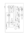
車両制御システム12000は、通信ネットワーク12001を介して接続された複数の電子制御ユニットを備える。図18に示した例では、車両制御システム12000は、駆動系制御ユニット12010、ボディ系制御ユニット12020、車外情報検出ユニット12030、車内情報検出ユニット12040、及び統合制御ユニット12050を備える。また、統合制御ユニット12050の機能構成として、マイクロコンピュータ12051、音声画像出力部12052、及び車載ネットワークI/F(interface)12053が図示されている。
駆動系制御ユニット12010は、各種プログラムにしたがって車両の駆動系に関連する装置の動作を制御する。例えば、駆動系制御ユニット12010は、内燃機関又は駆動用モータ等の車両の駆動力を発生させるための駆動力発生装置、駆動力を車輪に伝達するための駆動力伝達機構、車両の舵角を調節するステアリング機構、及び、車両の制動力を発生させる制動装置等の制御装置として機能する。
ボディ系制御ユニット12020は、各種プログラムにしたがって車体に装備された各種装置の動作を制御する。例えば、ボディ系制御ユニット12020は、キーレスエントリシステム、スマートキーシステム、パワーウィンドウ装置、あるいは、ヘッドランプ、バックランプ、ブレーキランプ、ウィンカー又はフォグランプ等の各種ランプの制御装置として機能する。この場合、ボディ系制御ユニット12020には、鍵を代替する携帯機から発信される電波又は各種スイッチの信号が入力され得る。ボディ系制御ユニット12020は、これらの電波又は信号の入力を受け付け、車両のドアロック装置、パワーウィンドウ装置、ランプ等を制御する。
車外情報検出ユニット12030は、車両制御システム12000を搭載した車両の外部の情報を検出する。例えば、車外情報検出ユニット12030には、撮像部12031が接続される。車外情報検出ユニット12030は、撮像部12031に車外の画像を撮像させるとともに、撮像された画像を受信する。車外情報検出ユニット12030は、受信した画像に基づいて、人、車、障害物、標識又は路面上の文字等の物体検出処理又は距離検出処理を行ってもよい。
撮像部12031は、光を受光し、その光の受光量に応じた電気信号を出力する光センサである。撮像部12031は、電気信号を画像として出力することもできるし、測距の情報として出力することもできる。また、撮像部12031が受光する光は、可視光であっても良いし、赤外線等の非可視光であっても良い。
車内情報検出ユニット12040は、車内の情報を検出する。車内情報検出ユニット12040には、例えば、運転者の状態を検出する運転者状態検出部12041が接続される。運転者状態検出部12041は、例えば運転者を撮像するカメラを含み、車内情報検出ユニット12040は、運転者状態検出部12041から入力される検出情報に基づいて、運転者の疲労度合い又は集中度合いを算出してもよいし、運転者が居眠りをしていないかを判別してもよい。
マイクロコンピュータ12051は、車外情報検出ユニット12030又は車内情報検出ユニット12040で取得される車内外の情報に基づいて、駆動力発生装置、ステアリング機構又は制動装置の制御目標値を演算し、駆動系制御ユニット12010に対して制御指令を出力することができる。例えば、マイクロコンピュータ12051は、車両の衝突回避あるいは衝撃緩和、車間距離に基づく追従走行、車速維持走行、車両の衝突警告、又は車両のレーン逸脱警告等を含むADAS(Advanced Driver Assistance System)の機能実現を目的とした協調制御を行うことができる。
また、マイクロコンピュータ12051は、車外情報検出ユニット12030又は車内情報検出ユニット12040で取得される車両の周囲の情報に基づいて駆動力発生装置、ステアリング機構又は制動装置等を制御することにより、運転者の操作に拠らずに自律的に走行する自動運転等を目的とした協調制御を行うことができる。
また、マイクロコンピュータ12051は、車外情報検出ユニット12030で取得される車外の情報に基づいて、ボディ系制御ユニット12020に対して制御指令を出力することができる。例えば、マイクロコンピュータ12051は、車外情報検出ユニット12030で検知した先行車又は対向車の位置に応じてヘッドランプを制御し、ハイビームをロービームに切り替える等の防眩を図ることを目的とした協調制御を行うことができる。
音声画像出力部12052は、車両の搭乗者又は車外に対して、視覚的又は聴覚的に情報を通知することが可能な出力装置へ音声及び画像のうちの少なくとも一方の出力信号を送信する。図18の例では、出力装置として、オーディオスピーカ12061、表示部12062及びインストルメントパネル12063が例示されている。表示部12062は、例えば、オンボードディスプレイ及びヘッドアップディスプレイの少なくとも一つを含んでいてもよい。
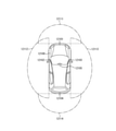
図19は、撮像部12031の設置位置の例を示す図である。
図19では、撮像部12031として、撮像部12101,12102,12103,12104,12105を有する。
撮像部12101,12102,12103,12104,12105は、例えば、車両12100のフロントノーズ、サイドミラー、リアバンパ、バックドア及び車室内のフロントガラスの上部等の位置に設けられる。フロントノーズに備えられる撮像部12101及び車室内のフロントガラスの上部に備えられる撮像部12105は、主として車両12100の前方の画像を取得する。サイドミラーに備えられる撮像部12102,12103は、主として車両12100の側方の画像を取得する。リアバンパ又はバックドアに備えられる撮像部12104は、主として車両12100の後方の画像を取得する。車室内のフロントガラスの上部に備えられる撮像部12105は、主として先行車両又は、歩行者、障害物、信号機、交通標識又は車線等の検出に用いられる。
なお、図19には、撮像部12101ないし12104の撮影範囲の一例が示されている。撮像範囲12111は、フロントノーズに設けられた撮像部12101の撮像範囲を示し、撮像範囲12112,12113は、それぞれサイドミラーに設けられた撮像部12102,12103の撮像範囲を示し、撮像範囲12114は、リアバンパ又はバックドアに設けられた撮像部12104の撮像範囲を示す。例えば、撮像部12101ないし12104で撮像された画像データが重ね合わせられることにより、車両12100を上方から見た俯瞰画像が得られる。
$
$
撮像部12101ないし12104の少なくとも1つは、距離情報を取得する機能を有していてもよい。例えば、撮像部12101ないし12104の少なくとも1つは、複数の撮像素子からなるステレオカメラであってもよいし、位相差検出用の画素を有する撮像素子であってもよい。
例えば、マイクロコンピュータ12051は、撮像部12101ないし12104から得られた距離情報を基に、撮像範囲12111ないし12114内における各立体物までの距離と、この距離の時間的変化(車両12100に対する相対速度)を求めることにより、特に車両12100の進行路上にある最も近い立体物で、車両12100と略同じ方向に所定の速度(例えば、0km/h以上)で走行する立体物を先行車として抽出することができる。さらに、マイクロコンピュータ12051は、先行車の手前に予め確保すべき車間距離を設定し、自動ブレーキ制御(追従停止制御も含む)や自動加速制御(追従発進制御も含む)等を行うことができる。このように運転者の操作に拠らずに自律的に走行する自動運転等を目的とした協調制御を行うことができる。
例えば、マイクロコンピュータ12051は、撮像部12101ないし12104から得られた距離情報を元に、立体物に関する立体物データを、2輪車、普通車両、大型車両、歩行者、電柱等その他の立体物に分類して抽出し、障害物の自動回避に用いることができる。例えば、マイクロコンピュータ12051は、車両12100の周辺の障害物を、車両12100のドライバが視認可能な障害物と視認困難な障害物とに識別する。そして、マイクロコンピュータ12051は、各障害物との衝突の危険度を示す衝突リスクを判断し、衝突リスクが設定値以上で衝突可能性がある状況であるときには、オーディオスピーカ12061や表示部12062を介してドライバに警報を出力することや、駆動系制御ユニット12010を介して強制減速や回避操舵を行うことで、衝突回避のための運転支援を行うことができる。
撮像部12101ないし12104の少なくとも1つは、赤外線を検出する赤外線カメラであってもよい。例えば、マイクロコンピュータ12051は、撮像部12101ないし12104の撮像画像中に歩行者が存在するか否かを判定することで歩行者を認識することができる。かかる歩行者の認識は、例えば赤外線カメラとしての撮像部12101ないし12104の撮像画像における特徴点を抽出する手順と、物体の輪郭を示す一連の特徴点にパターンマッチング処理を行って歩行者か否かを判別する手順によって行われる。マイクロコンピュータ12051が、撮像部12101ないし12104の撮像画像中に歩行者が存在すると判定し、歩行者を認識すると、音声画像出力部12052は、当該認識された歩行者に強調のための方形輪郭線を重畳表示するように、表示部12062を制御する。また、音声画像出力部12052は、歩行者を示すアイコン等を所望の位置に表示するように表示部12062を制御してもよい。
以上、本開示に係る技術が適用され得る車両制御システムの一例について説明した。本開示に係る技術は、以上説明した構成のうち、撮像部12031に適用され得る。具体的には、図1の送信回路100は、撮像部12031の通信インターフェースに適用することができる。撮像部12031に本開示に係る技術を適用することにより、振幅の制御精度の向上によって信号品質を向上させることができる。
なお、上述の実施の形態は本技術を具現化するための一例を示したものであり、実施の形態における事項と、特許請求の範囲における発明特定事項とはそれぞれ対応関係を有する。同様に、特許請求の範囲における発明特定事項と、これと同一名称を付した本技術の実施の形態における事項とはそれぞれ対応関係を有する。ただし、本技術は実施の形態に限定されるものではなく、その要旨を逸脱しない範囲において実施の形態に種々の変形を施すことにより具現化することができる。
なお、本明細書に記載された効果はあくまで例示であって、限定されるものではなく、また、他の効果があってもよい。
なお、本技術は以下のような構成もとることができる。
(1)所定の参照電圧から一対の電圧の一方を生成してドライバの電源端子および接地端子の一方に供給する第1の電圧レギュレータと、
前記一対の電圧の一方から前記一対の電圧の他方を生成して前記電源端子および前記接地端子の他方に供給する第2の電圧レギュレータと
を具備する制御回路。
(2)前記第1の電圧レギュレータは、前記一対の電圧のうち低い方を生成し、
前記第2の電圧レギュレータは、前記一対の電圧のうち高い方を生成する
前記(1)記載の制御回路。
(3)前記第1の電圧レギュレータは、前記一対の電圧のうち高い方を生成し、
前記第2の電圧レギュレータは、前記一対の電圧のうち低い方を生成する
前記(1)記載の制御回路。
(4)前記参照電圧を生成して前記第1の電圧レギュレータに供給する参照電圧生成回路をさらに具備する前記(1)から(3)のいずれかに記載の制御回路。
(5)前記参照電圧生成回路は、所定の接地電圧を基準として前記参照電圧を生成する
前記(4)記載の制御回路。
(6)前記参照電圧生成回路は、所定の電源電圧を基準として前記参照電圧を生成する
前記(4)記載の制御回路。
(7)前記第1の電圧レギュレータは、
前記一対の電圧の一方を出力する第1オペアンプと、
前記第1オペアンプの一対の入力端子の一方と前記電源端子および前記接地端子の一方との間に挿入された第1抵抗と、
前記一対の入力端子の一方に一端が接続された第2抵抗と
を備え、
前記一対の入力端子の他方には、前記参照電圧が入力される
前記(1)から(6)のいずれかに記載の制御回路。
(8)前記第2抵抗の他端には、所定の接地電圧が印加される
前記(7)記載の制御回路。
(9)前記第2抵抗の他端には、所定の電源電圧が印加される
前記(7)記載の制御回路。
(10)前記第2の電圧レギュレータは、
前記一対の電圧の他方を出力する第2オペアンプと、
前記第2オペアンプの一対の入力端子の一方と前記電源端子および前記接地端子の他方との間に挿入された第3抵抗と、
前記一対の入力端子の一方に一端が接続された第4抵抗と
を備え、
前記一対の入力端子の他方には、前記一対の電圧の一方に応じた電圧が印加される
前記(7)に記載の制御回路。
(11)前記第4抵抗の他端には、前記一対の電圧の一方が印加される
前記(10)記載の制御回路。
(12)前記第4抵抗の他端には、所定の電源電圧が印加される
前記(10)記載の制御回路。
(13)ドライバと、
所定の参照電圧から一対の電圧の一方を生成して前記ドライバの電源端子および接地端子の一方に供給する第1の電圧レギュレータと、
前記一対の電圧の一方から前記一対の電圧の他方を生成して前記電源端子および前記接地端子の他方に供給する第2の電圧レギュレータと
を具備する駆動回路。
(1)所定の参照電圧から一対の電圧の一方を生成してドライバの電源端子および接地端子の一方に供給する第1の電圧レギュレータと、
前記一対の電圧の一方から前記一対の電圧の他方を生成して前記電源端子および前記接地端子の他方に供給する第2の電圧レギュレータと
を具備する制御回路。
(2)前記第1の電圧レギュレータは、前記一対の電圧のうち低い方を生成し、
前記第2の電圧レギュレータは、前記一対の電圧のうち高い方を生成する
前記(1)記載の制御回路。
(3)前記第1の電圧レギュレータは、前記一対の電圧のうち高い方を生成し、
前記第2の電圧レギュレータは、前記一対の電圧のうち低い方を生成する
前記(1)記載の制御回路。
(4)前記参照電圧を生成して前記第1の電圧レギュレータに供給する参照電圧生成回路をさらに具備する前記(1)から(3)のいずれかに記載の制御回路。
(5)前記参照電圧生成回路は、所定の接地電圧を基準として前記参照電圧を生成する
前記(4)記載の制御回路。
(6)前記参照電圧生成回路は、所定の電源電圧を基準として前記参照電圧を生成する
前記(4)記載の制御回路。
(7)前記第1の電圧レギュレータは、
前記一対の電圧の一方を出力する第1オペアンプと、
前記第1オペアンプの一対の入力端子の一方と前記電源端子および前記接地端子の一方との間に挿入された第1抵抗と、
前記一対の入力端子の一方に一端が接続された第2抵抗と
を備え、
前記一対の入力端子の他方には、前記参照電圧が入力される
前記(1)から(6)のいずれかに記載の制御回路。
(8)前記第2抵抗の他端には、所定の接地電圧が印加される
前記(7)記載の制御回路。
(9)前記第2抵抗の他端には、所定の電源電圧が印加される
前記(7)記載の制御回路。
(10)前記第2の電圧レギュレータは、
前記一対の電圧の他方を出力する第2オペアンプと、
前記第2オペアンプの一対の入力端子の一方と前記電源端子および前記接地端子の他方との間に挿入された第3抵抗と、
前記一対の入力端子の一方に一端が接続された第4抵抗と
を備え、
前記一対の入力端子の他方には、前記一対の電圧の一方に応じた電圧が印加される
前記(7)に記載の制御回路。
(11)前記第4抵抗の他端には、前記一対の電圧の一方が印加される
前記(10)記載の制御回路。
(12)前記第4抵抗の他端には、所定の電源電圧が印加される
前記(10)記載の制御回路。
(13)ドライバと、
所定の参照電圧から一対の電圧の一方を生成して前記ドライバの電源端子および接地端子の一方に供給する第1の電圧レギュレータと、
前記一対の電圧の一方から前記一対の電圧の他方を生成して前記電源端子および前記接地端子の他方に供給する第2の電圧レギュレータと
を具備する駆動回路。
100 送信回路
110 送信信号生成部
200 駆動回路
210 制御回路
220 高電圧側電圧レギュレータ
221、232、246 電流源
222、225、231、243、245 抵抗
223、241 オペアンプ
224 pMOSトランジスタ
226、244 可変抵抗
230 参照電圧生成回路
240 低電圧側電圧レギュレータ
242 nMOSトランジスタ
250 ドライバ
300 受信回路
12031 撮像部
110 送信信号生成部
200 駆動回路
210 制御回路
220 高電圧側電圧レギュレータ
221、232、246 電流源
222、225、231、243、245 抵抗
223、241 オペアンプ
224 pMOSトランジスタ
226、244 可変抵抗
230 参照電圧生成回路
240 低電圧側電圧レギュレータ
242 nMOSトランジスタ
250 ドライバ
300 受信回路
12031 撮像部
Claims (13)
- 所定の参照電圧から一対の電圧の一方を生成してドライバの電源端子および接地端子の一方に供給する第1の電圧レギュレータと、
前記一対の電圧の一方から前記一対の電圧の他方を生成して前記電源端子および前記接地端子の他方に供給する第2の電圧レギュレータと
を具備する制御回路。 - 前記第1の電圧レギュレータは、前記一対の電圧のうち低い方を生成し、
前記第2の電圧レギュレータは、前記一対の電圧のうち高い方を生成する
請求項1記載の制御回路。 - 前記第1の電圧レギュレータは、前記一対の電圧のうち高い方を生成し、
前記第2の電圧レギュレータは、前記一対の電圧のうち低い方を生成する
請求項1記載の制御回路。 - 前記参照電圧を生成して前記第1の電圧レギュレータに供給する参照電圧生成回路をさらに具備する請求項1記載の制御回路。
- 前記参照電圧生成回路は、所定の接地電圧を基準として前記参照電圧を生成する
請求項4記載の制御回路。 - 前記参照電圧生成回路は、所定の電源電圧を基準として前記参照電圧を生成する
請求項4記載の制御回路。 - 前記第1の電圧レギュレータは、
前記一対の電圧の一方を出力する第1オペアンプと、
前記第1オペアンプの一対の入力端子の一方と前記電源端子および前記接地端子の一方との間に挿入された第1抵抗と、
前記一対の入力端子の一方に一端が接続された第2抵抗と
を備え、
前記一対の入力端子の他方には、前記参照電圧が入力される
請求項1記載の制御回路。 - 前記第2抵抗の他端には、所定の接地電圧が印加される
請求項7記載の制御回路。 - 前記第2抵抗の他端には、所定の電源電圧が印加される
請求項7記載の制御回路。 - 前記第2の電圧レギュレータは、
前記一対の電圧の他方を出力する第2オペアンプと、
前記第2オペアンプの一対の入力端子の一方と前記電源端子および前記接地端子の他方との間に挿入された第3抵抗と、
前記一対の入力端子の一方に一端が接続された第4抵抗と
を備え、
前記一対の入力端子の他方には、前記一対の電圧の一方に応じた電圧が印加される
請求項7記載の制御回路。 - 前記第4抵抗の他端には、前記一対の電圧の一方が印加される
請求項10記載の制御回路。 - 前記第4抵抗の他端には、所定の電源電圧が印加される
請求項10記載の制御回路。 - ドライバと、
所定の参照電圧から一対の電圧の一方を生成して前記ドライバの電源端子および接地端子の一方に供給する第1の電圧レギュレータと、
前記一対の電圧の一方から前記一対の電圧の他方を生成して前記電源端子および前記接地端子の他方に供給する第2の電圧レギュレータと
を具備する駆動回路。
Priority Applications (2)
| Application Number | Priority Date | Filing Date | Title |
|---|---|---|---|
| US18/043,079 US20230318604A1 (en) | 2020-09-07 | 2021-07-08 | Control circuit and driving circuit |
| JP2022546909A JP7717077B2 (ja) | 2020-09-07 | 2021-07-08 | 制御回路および駆動回路 |
Applications Claiming Priority (2)
| Application Number | Priority Date | Filing Date | Title |
|---|---|---|---|
| JP2020149817 | 2020-09-07 | ||
| JP2020-149817 | 2020-09-07 |
Publications (1)
| Publication Number | Publication Date |
|---|---|
| WO2022049893A1 true WO2022049893A1 (ja) | 2022-03-10 |
Family
ID=80491098
Family Applications (1)
| Application Number | Title | Priority Date | Filing Date |
|---|---|---|---|
| PCT/JP2021/025759 Ceased WO2022049893A1 (ja) | 2020-09-07 | 2021-07-08 | 制御回路および駆動回路 |
Country Status (3)
| Country | Link |
|---|---|
| US (1) | US20230318604A1 (ja) |
| JP (1) | JP7717077B2 (ja) |
| WO (1) | WO2022049893A1 (ja) |
Citations (7)
| Publication number | Priority date | Publication date | Assignee | Title |
|---|---|---|---|---|
| JPH11150469A (ja) * | 1997-09-11 | 1999-06-02 | Mitsubishi Electric Corp | 半導体集積回路 |
| JP2000041072A (ja) * | 1998-05-14 | 2000-02-08 | Natl Semiconductor Corp <Ns> | バックプレ―ン適用用のlvdsドライバ |
| JP2005223872A (ja) * | 2004-01-05 | 2005-08-18 | Thine Electronics Inc | 差動駆動回路およびそれを内蔵する電子機器 |
| US7330056B1 (en) * | 2005-12-06 | 2008-02-12 | Exar Corporation | Low power CMOS LVDS driver |
| JP2014064272A (ja) * | 2012-09-03 | 2014-04-10 | Mega Chips Corp | 出力バッファ回路 |
| JP2015018364A (ja) * | 2013-07-10 | 2015-01-29 | スパンション エルエルシー | 電源装置及び半導体装置 |
| JP2019527983A (ja) * | 2016-08-03 | 2019-10-03 | ザイリンクス インコーポレイテッドXilinx Incorporated | 電圧モードドライバのインピーダンスおよびスイング制御 |
Family Cites Families (6)
| Publication number | Priority date | Publication date | Assignee | Title |
|---|---|---|---|---|
| JPH04252514A (ja) * | 1990-02-28 | 1992-09-08 | Nec Corp | 出力バッファ回路 |
| US7012450B1 (en) * | 2003-12-15 | 2006-03-14 | Decicon, Inc. | Transmitter for low voltage differential signaling |
| WO2006117860A1 (ja) | 2005-04-28 | 2006-11-09 | Thine Electronics, Inc. | 差動駆動回路およびそれを内蔵する電子機器 |
| US7898295B1 (en) * | 2009-03-19 | 2011-03-01 | Pmc-Sierra, Inc. | Hot-pluggable differential signaling driver |
| AU2011284808A1 (en) | 2010-07-30 | 2013-02-21 | Newsouth Innovations Pty Limited | Current recycling in multiple linear regulators |
| US10056777B2 (en) | 2016-06-24 | 2018-08-21 | Qualcomm Incorporated | Voltage mode driver with charge recycling |
-
2021
- 2021-07-08 US US18/043,079 patent/US20230318604A1/en not_active Abandoned
- 2021-07-08 JP JP2022546909A patent/JP7717077B2/ja active Active
- 2021-07-08 WO PCT/JP2021/025759 patent/WO2022049893A1/ja not_active Ceased
Patent Citations (7)
| Publication number | Priority date | Publication date | Assignee | Title |
|---|---|---|---|---|
| JPH11150469A (ja) * | 1997-09-11 | 1999-06-02 | Mitsubishi Electric Corp | 半導体集積回路 |
| JP2000041072A (ja) * | 1998-05-14 | 2000-02-08 | Natl Semiconductor Corp <Ns> | バックプレ―ン適用用のlvdsドライバ |
| JP2005223872A (ja) * | 2004-01-05 | 2005-08-18 | Thine Electronics Inc | 差動駆動回路およびそれを内蔵する電子機器 |
| US7330056B1 (en) * | 2005-12-06 | 2008-02-12 | Exar Corporation | Low power CMOS LVDS driver |
| JP2014064272A (ja) * | 2012-09-03 | 2014-04-10 | Mega Chips Corp | 出力バッファ回路 |
| JP2015018364A (ja) * | 2013-07-10 | 2015-01-29 | スパンション エルエルシー | 電源装置及び半導体装置 |
| JP2019527983A (ja) * | 2016-08-03 | 2019-10-03 | ザイリンクス インコーポレイテッドXilinx Incorporated | 電圧モードドライバのインピーダンスおよびスイング制御 |
Also Published As
| Publication number | Publication date |
|---|---|
| US20230318604A1 (en) | 2023-10-05 |
| JPWO2022049893A1 (ja) | 2022-03-10 |
| JP7717077B2 (ja) | 2025-08-01 |
Similar Documents
| Publication | Publication Date | Title |
|---|---|---|
| EP3737084B1 (en) | Solid-state imaging element, imaging device, and method for controlling solid-state imaging element | |
| CN113396579A (zh) | 事件信号检测传感器和控制方法 | |
| WO2019039312A1 (ja) | 駆動装置、駆動方法、及び、発光装置 | |
| JP2020162000A (ja) | データ処理装置、データ処理方法、及び、プログラム | |
| WO2017195459A1 (ja) | 撮像装置、および撮像方法 | |
| WO2019044487A1 (ja) | 測距装置、及び、測距方法 | |
| US12536997B2 (en) | Information processing device and information processing method | |
| US11575545B2 (en) | Transmission device, interface, and transmission method | |
| CN111587572A (zh) | 图像处理装置、图像处理方法和程序 | |
| JP7717077B2 (ja) | 制御回路および駆動回路 | |
| WO2017203752A1 (ja) | 撮像装置、および制御方法 | |
| JP7713520B2 (ja) | 駆動回路 | |
| US12556836B2 (en) | Semiconductor integrated circuit, electronic device, and method for controlling semiconductor integrated circuit | |
| WO2022153746A1 (ja) | 撮像装置 | |
| US12604112B2 (en) | Semiconductor circuit, imaging device, and electronic device | |
| WO2022190475A1 (ja) | 静電気放電保護回路、および、電子装置 | |
| WO2021256483A1 (ja) | 制御装置、投影システム、制御方法及びプログラム | |
| JP2020072316A (ja) | 電子回路、固体撮像素子、および、電子回路の制御方法 | |
| US20250301242A1 (en) | Imaging device and charge pump circuit | |
| WO2025062889A1 (ja) | 撮像装置 | |
| WO2025057566A1 (ja) | 固体撮像素子、電子機器、および、固体撮像素子の制御方法 | |
| WO2018179646A1 (ja) | 遠赤外線撮像装置 | |
| WO2022137993A1 (ja) | コンパレータ及び固体撮像素子 | |
| WO2021193168A1 (ja) | 撮像装置 | |
| JP2022157423A (ja) | 固体撮像素子及び固体撮像装置 |
Legal Events
| Date | Code | Title | Description |
|---|---|---|---|
| 121 | Ep: the epo has been informed by wipo that ep was designated in this application |
Ref document number: 21863951 Country of ref document: EP Kind code of ref document: A1 |
|
| ENP | Entry into the national phase |
Ref document number: 2022546909 Country of ref document: JP Kind code of ref document: A |
|
| NENP | Non-entry into the national phase |
Ref country code: DE |
|
| 122 | Ep: pct application non-entry in european phase |
Ref document number: 21863951 Country of ref document: EP Kind code of ref document: A1 |