WO2022044686A1 - Apdセンサ及び測距システム - Google Patents
Apdセンサ及び測距システム Download PDFInfo
- Publication number
- WO2022044686A1 WO2022044686A1 PCT/JP2021/028163 JP2021028163W WO2022044686A1 WO 2022044686 A1 WO2022044686 A1 WO 2022044686A1 JP 2021028163 W JP2021028163 W JP 2021028163W WO 2022044686 A1 WO2022044686 A1 WO 2022044686A1
- Authority
- WO
- WIPO (PCT)
- Prior art keywords
- pixel
- output
- apd
- circuit
- phase comparison
- Prior art date
- Legal status (The legal status is an assumption and is not a legal conclusion. Google has not performed a legal analysis and makes no representation as to the accuracy of the status listed.)
- Ceased
Links
Images











Classifications
-
- G—PHYSICS
- G01—MEASURING; TESTING
- G01C—MEASURING DISTANCES, LEVELS OR BEARINGS; SURVEYING; NAVIGATION; GYROSCOPIC INSTRUMENTS; PHOTOGRAMMETRY OR VIDEOGRAMMETRY
- G01C3/00—Measuring distances in line of sight; Optical rangefinders
- G01C3/02—Details
- G01C3/06—Use of electric means to obtain final indication
-
- G—PHYSICS
- G01—MEASURING; TESTING
- G01S—RADIO DIRECTION-FINDING; RADIO NAVIGATION; DETERMINING DISTANCE OR VELOCITY BY USE OF RADIO WAVES; LOCATING OR PRESENCE-DETECTING BY USE OF THE REFLECTION OR RERADIATION OF RADIO WAVES; ANALOGOUS ARRANGEMENTS USING OTHER WAVES
- G01S17/00—Systems using the reflection or reradiation of electromagnetic waves other than radio waves, e.g. lidar systems
- G01S17/88—Lidar systems specially adapted for specific applications
- G01S17/89—Lidar systems specially adapted for specific applications for mapping or imaging
- G01S17/894—Three-dimensional [3D] imaging with simultaneous measurement of time-of-flight at a two-dimensional [2D] array of receiver pixels, e.g. time-of-flight cameras or flash lidar
-
- G—PHYSICS
- G01—MEASURING; TESTING
- G01S—RADIO DIRECTION-FINDING; RADIO NAVIGATION; DETERMINING DISTANCE OR VELOCITY BY USE OF RADIO WAVES; LOCATING OR PRESENCE-DETECTING BY USE OF THE REFLECTION OR RERADIATION OF RADIO WAVES; ANALOGOUS ARRANGEMENTS USING OTHER WAVES
- G01S17/00—Systems using the reflection or reradiation of electromagnetic waves other than radio waves, e.g. lidar systems
- G01S17/88—Lidar systems specially adapted for specific applications
- G01S17/93—Lidar systems specially adapted for specific applications for anti-collision purposes
- G01S17/931—Lidar systems specially adapted for specific applications for anti-collision purposes of land vehicles
-
- G—PHYSICS
- G01—MEASURING; TESTING
- G01S—RADIO DIRECTION-FINDING; RADIO NAVIGATION; DETERMINING DISTANCE OR VELOCITY BY USE OF RADIO WAVES; LOCATING OR PRESENCE-DETECTING BY USE OF THE REFLECTION OR RERADIATION OF RADIO WAVES; ANALOGOUS ARRANGEMENTS USING OTHER WAVES
- G01S7/00—Details of systems according to groups G01S13/00, G01S15/00, G01S17/00
- G01S7/48—Details of systems according to groups G01S13/00, G01S15/00, G01S17/00 of systems according to group G01S17/00
- G01S7/483—Details of pulse systems
- G01S7/486—Receivers
- G01S7/4861—Circuits for detection, sampling, integration or read-out
- G01S7/4863—Detector arrays, e.g. charge-transfer gates
Definitions
- This disclosure relates to APD sensors and ranging systems.
- LiDAR Light Detection and Ringing
- APD Avalanche Photo Diode
- SPAD Single Photon Avalanche Diode
- APD causes avalanche amplification by colliding photons with a light receiving part to which a strong electric field is applied, and this effect can cause a large potential change even with weak incident light.
- SPAD is capable of detecting in units of one photon.
- APD requires a recharge time after detecting light, and there is a dead time. During this dead time period, the APD will not be able to detect the next photon.
- the housing used for LiDAR is often equipped with both a light source and a light receiving element inside. Therefore, the light emitted from the light source may be reflected in the housing, and stray light incident on the light receiving element may be generated.
- the element When the APD is used as a light receiving element, the element is turned on by applying a voltage higher than the breakdown to the APD so that photons can be detected.
- this voltage By applying this voltage, it is possible to make it possible to detect photons, but if this timing is early, the photons reflected inside the housing will be incident on the APD, and the photons will be emitted before receiving the reflected light from the target. It may correspond to the dead time period at the timing of detecting and receiving the reflected light from the target. On the other hand, if the timing of applying this voltage is late, the charging is not completed at the timing of receiving the reflected light from the target, and the light reflected from the target cannot be detected properly.
- timing control circuit for controlling the on / off of the APD in the light receiving sensor
- accurate timing control is possible at the control circuit output, but the delay of the driver driving the control signal of the pixel array and the control signal. Since the delay of the level shifter that converts the APD into the pixel drive voltage, the recharge time of the APD, and the like depend on the variation of the element and the temperature / power supply voltage, it is difficult to actually control the timing at which the APD is turned on.
- an APD sensor that improves the accuracy of APD drive timing is realized.
- the APD sensor has a first pixel having an APD as a light receiving element and used for receiving light, a second pixel having an APD as a light receiving element and not used for receiving light, and the first pixel or the first pixel or the like.
- the delay circuit may delay the enable signal to synchronize the reference pulse with the timing at which the voltage that enables the output of the light receiving element in the first pixel is charged.
- the delay circuit may delay the enable signal that charges the anode or cathode of the APD with a voltage for driving a light receiving state.
- the phase comparison circuit may include a D-FF in which the output of the first pixel or the second pixel is input to the D terminal, the reference pulse signal is input to the clock terminal, and the output is output from the Q terminal. ..
- the delay circuit may output the enable signal with a longer delay as compared with the case where the output of the phase comparison circuit is high. ..
- the phase comparison circuit may be a TDC that converts the time difference between the output of at least one of the first pixel or the second pixel and the reference pulse signal into a multi-bit digital signal.
- the first pixel is provided in an array in a second direction which is a direction intersecting the first direction and the first direction, and the second pixel is provided in a plurality of the first pixels provided along the first direction.
- the second pixel may be provided in the pixel array closer to the phase comparison circuit in terms of wiring than the first pixel along each of the first directions, and the phase comparison circuit may be provided.
- the output of the second pixel and the reference pulse may be compared and output.
- a semiconductor substrate comprising a first substrate comprising the APD, a phase comparison circuit, and a second substrate comprising at least the delay circuit and laminated with the first substrate. You may.
- the distance measuring system includes the above-mentioned APD sensor and a light emitting element, and the light emitted from the light emitting element receives the light reflected by the subject by the first pixel, and the light is emitted.
- the distance to the subject is measured based on the timing at which the element emits light and the timing at which the first pixel receives light.
- a circuit diagram schematically showing an APD sensor according to an embodiment A circuit diagram schematically showing an APD sensor according to an embodiment. The figure which shows typically the layout which concerns on one Embodiment.
- a circuit diagram schematically showing a light receiving pixel according to an embodiment A circuit diagram schematically showing a light receiving pixel according to an embodiment.
- a circuit diagram schematically showing a light receiving pixel according to an embodiment The figure which shows typically the timing chart of the APD sensor which concerns on one Embodiment.
- a circuit diagram schematically showing a light receiving pixel according to an embodiment A circuit diagram schematically showing a light receiving pixel according to an embodiment.
- a circuit diagram schematically showing a light receiving pixel according to an embodiment A circuit diagram schematically showing a light receiving pixel according to an embodiment.
- a circuit diagram schematically showing a light receiving pixel according to an embodiment It is a block diagram which shows an example of the schematic structure of a vehicle control system. It is explanatory drawing which shows an example of the installation position of the vehicle outside information detection unit and the image pickup
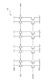
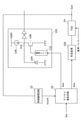
- FIG. 1 is a circuit diagram schematically showing an APD (Avalanche Photodiode) sensor according to an embodiment.
- the APD sensor 1 includes, for example, a pixel array 10, a delay circuit 12, a phase comparison circuit 14, and a pulse oscillation circuit 16.
- the APD sensor 1 is a circuit that converts light incident on a light receiving element included in the pixel array 10 into a signal and outputs it.
- FIG. 1 the control regarding light reception is shown, and the output of the signal is not shown, but it is assumed that a circuit for appropriately outputting is provided. Further, although the signal lines and the like from the delay circuit 12 to each pixel of the pixel array 10 are omitted, it is assumed that they are also appropriately provided. For example, signals may be sequentially given from the delay circuit 12 in the horizontal direction (line direction) in the figure.
- the pixel array 10 includes effective pixels 100 (first pixel) and dummy pixels 102 (second pixel) in an array along the first and second directions. A plurality of effective pixels 100 and a plurality of dummy pixels 102 are provided. As shown in the figure, the pixel array 10 includes, for example, dummy pixels 102 in a region closer to the phase comparison circuit 14 than the effective pixels 100.
- the effective pixel 100 is a pixel that receives light reception, and when light is received by the effective pixel 100, this light is converted into a signal and output.
- the effective pixel 100 is configured to include, for example, a SPAD (Single Photon Avalanche Diode).
- the dummy pixel 102 is a pixel that does not accept light reception and is a pixel used for timing control.
- the dummy pixel 102 is basically configured to have the same SPAD as the effective pixel 100, but is arranged so as not to be able to receive light or to convert the received light into a signal, for example.
- the dummy pixel 102 is arranged so that the light receiving surface of the SPAD is shielded from light or the anode of the SPAD is connected to the ground potential.
- the dummy pixel 102 outputs a signal to the phase comparison circuit 14 at the timing when the SPAD electrons released by the control from the delay circuit 12 are charged. Since the control signal of the delay circuit 12 is delayed based on the state of the dummy circuit 102, it is desirable to reduce the delay by reducing the distance between the dummy circuit 102 and the phase comparison circuit 14. For example, in the case of the structure as shown in FIG. 1, it is desirable that the dummy circuit 102 is arranged at a position closer to the phase comparison circuit 14 than the effective pixel 100 along the first direction.
- the delay circuit 12 is a circuit that outputs a signal for controlling light reception of the effective pixels 100 and the dummy pixels 102 provided in the pixel array 10. For example, the delay circuit 12 outputs a signal for controlling the effective pixels 100 and the dummy pixels 102 arranged in the second directions for each line.
- the effective pixel 100 and the dummy pixel 102 start receiving light based on the control signal output from the delay circuit 12 for each line, and when the light is received, the SPAD converts the light into a signal and outputs the light appropriately. ..
- the phase comparison circuit 14 compares and outputs the phase difference between the signal output from the dummy circuit 102 and the signal received from the pulse oscillation circuit 16.
- the delay circuit 12 delays the control signal and outputs it to the pixel based on the phase difference output by the phase comparison circuit 14.
- the delay circuit 12 delays the control signal and outputs it to the pixel based on the phase difference output by the phase comparison circuit 14.
- phase comparison circuit 14 is shown as one circuit, it may be provided for each dummy pixel 102 or for each column.
- one dummy pixel 102 may be provided for one column, and a phase comparison circuit 14 may be provided for each of the dummy pixels 102.
- the present invention is not limited to this configuration, as long as the operation described below can be appropriately executed.
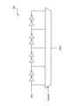
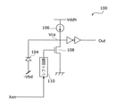
- FIG. 2 is a diagram showing an example of connection of the dummy pixel 102 according to the present embodiment.
- a circuit whose voltage is appropriately adjusted for example, a buffer circuit or the like may be provided.
- a buffer circuit may be provided between the delay circuit 12, the effective pixel 100, and the dummy pixel 102.
- the dummy pixel 102 When the charging is completed, the dummy pixel 102 outputs the signal as a dummy signal Out_dummy. This signal is input to the phase comparison circuit 14.
- This dummy signal and the reference pulse output from the pulse oscillation circuit 16 are input to the phase comparison circuit 14.
- the phase comparison circuit 14 outputs the delay of the dummy signal with respect to the pulse signal as the phase difference.
- the charge pump 18 increases or decreases the voltage based on this phase difference signal and outputs it.
- the charge pump 18 raises Vcont when the output of the phase comparison circuit 14 is High (on), and conversely, Vcont when the output of the phase comparison circuit 14 is Low (off). Is lowered and output.
- This voltage control is executed, for example, depending on whether the output of the phase comparison circuit 14 is High or Low at the timing when the clock signal is input.
- the charge pump 18 may be provided in the phase comparison circuit 14, and may not be provided if the signal output by the phase comparison circuit 14 causes a sufficient potential difference in Vcont at the on / off timing. You may.
- the delay circuit 12 outputs the delayed signal Xen of the control signal Xin to each pixel based on the phase difference signal output by the phase comparison circuit 14. As described above, the output is, for example, a control voltage as a signal for each line.
- the dummy pixel 102 includes, for example, a SPAD 104, a current source 106, an n-type MOSFET (Metal-Oxide-Semiconductor Field-Effect-Transistor, hereinafter referred to as nMOS 108), and a shift circuit 110.
- nMOS 108 Metal-Oxide-Semiconductor Field-Effect-Transistor
- This configuration is basically the same for the effective pixel 100.
- the light receiving surface of the SPAD 104 is set to be shielded from light so that the pixel signal due to the light reception is not output.
- the current source 106 is connected to, for example, the power supply voltage Vddh, and charges the carrier on the cathode side of the SPAD 104. This charge causes the SPAD 104 after discharge to transition to a state where it can receive light.
- the nMOS 108 is a switch for discharging the cathode of the SPAD 104 after a signal is output from the SPAD 104, and is turned on / off at a predetermined timing to control the charging / discharging of the cathode side of the SPAD 104.
- the delay circuit 12 outputs a drive signal for controlling the nMOS 108.
- the shift circuit 110 is a circuit that changes the reference level of the voltage output by the delay circuit 12 to the reference level of the voltage of nMOS 108.
- a commonly used level shift circuit can be appropriately used for the shift circuit 110.
- the dummy pixel 102 discharges the voltage Vca on the cathode side of the SPAD 104 to the reference voltage (for example, the ground potential) at the timing when the control signal is turned on from the delay circuit 12. Then, the voltage Vca is charged to a predetermined voltage at the timing when the control signal from the delay circuit 12 is turned off.
- the reference voltage for example, the ground potential
- the dummy pixel 102 outputs a signal when the voltage Vca exceeds a predetermined voltage due to the buffer.
- This predetermined voltage is the voltage applied to the cathode side in order to start SPAD 104.
- the phase comparison circuit 14 When the signal is output from the dummy pixel 102, the phase comparison circuit 14 outputs the phase difference from the reference pulse.
- the delay circuit 12 outputs the control signal Xen based on this phase difference, for example, adjusting the delay from the laser emission timing in the ToF (Time of Flight) sensor.
- FIG. 3 is a diagram schematically showing a timing chart according to this embodiment.
- the light emission trigger in the uppermost stage is a trigger signal indicating the irradiation timing of the laser in the ToF sensor. Based on this light emission trigger, the laser is radiated to the subject.
- Xen is a control signal that controls the output from the pixels.
- Let td_LD be the time from this Xen to the light emission trigger.
- Vca is the voltage on the cathode side of SPAD 104.
- the time from when the control signal Xen is turned off until the SPAD 104 is ready to receive light is defined as td_wakeup.
- td_wakeup time elapses after the control signal Xen is input, the SPAD 104 is ready to receive light.
- the SPAD 104 can properly receive the photons reflected from the subject.
- timing when SPAD is turned on is early, for example, if td_LD is the same time as td_wakeup, after SPAD is turned on, SPAD 104 receives the photon due to the reflection inside the housing, and the subsequent SPAD is dead time. The reflected light from the subject is received at the timing when. At such a timing, it is not possible to output a signal due to the reflected light in the housing and appropriately receive the reflected light from the subject. Therefore, the correct distance cannot be measured.
- control for delaying Xen is executed based on the time (td_wakeup) at which charging ends in the dummy pixel 102.
- the phase comparison circuit 14 is provided with, for example, D-FF (D-Flip Flop) in order to output the control signal Xen as shown above.
- D-FF D-Flip Flop
- the output of the dummy pixel 102 is connected to the D terminal of the D-FF, and the reference pulse is input to the clock terminal.
- the output of the phase comparison circuit 14 is Low because the output from the dummy pixel 102 is off at the timing when the reference pulse is input.
- the output of the phase comparison circuit 14 becomes High because the output from the dummy pixel 102 is turned on at the timing when the reference pulse is input.
- the output of the phase comparison circuit 14 is input to the charge pump 18 and boosted. If the circuit can appropriately control the voltage output according to the high and low pulse signals, it can be used instead of the charge pump.
- the voltage Vcont is output from the phase comparison circuit 14 or the charge pump 18 to the delay circuit 12.
- FIG. 4 is a circuit diagram schematically showing the delay circuit 12 according to the present embodiment.
- the delay circuit 12 is a circuit in which an even number of inverters are connected in series. Xin, which is an enable signal, is input to the input of the inverter, and Xen, which is a delayed enable signal, is output from the last inverter. This Xen is output to the effective pixel 100 and the dummy pixel 102. More specifically, as shown in FIG. 1, it is output as a signal for pixels along the line.
- the figure is shown as an example, and the number of inverters included in the delay circuit 12 may be any number that does not invert on / off.
- Each inverter is connected to Vdd and Vss as the power supply voltage. Between the inverter and Vss, for example, nMOS to which the voltage Vcont is connected to the gate is connected. When the voltage Vcont is high, the current flowing through the inverter increases, so the delay time becomes short. On the other hand, when the voltage Vcont is low, the current flowing through the inverter is small, so that the delay time becomes long.
- the rise time of the light receiving possible period of the SPAD 104 of the dummy pixel 102 is delayed from the current state.
- the rise time of the light receiving possible period of the SPAD 104 of the dummy pixel 102 is made faster than the current state.
- a DLL Delay Locked Loop
- the APD sensor 1 adjusts the on-timing of SPAD by this DLL.
- Each circuit element is appropriately selected so that the delay of the output of the above enable signal becomes the circuit constant in the state shown in FIG.
- the present embodiment it is possible to appropriately set the light receiving possible period of the SPAD 104 in the pixel, and it is possible to avoid the influence of stray light and the like.
- FIG. 1 by making the wiring of the dummy pixel 102 and the phase comparison circuit 14 shorter than the effective pixel 100, it is possible to suppress the delay in the wiring of the signal from the dummy pixel 102 to the phase comparison circuit 14. Is. Therefore, the start-up time of SPAD in the pixel can be more accurately reflected in the enable signal.
- the delay for each column can be appropriately detected in the dummy pixel 102. Therefore, when the back enable signal Xen delayed from the control circuit 12 is output for each line, it is possible to appropriately reflect the wiring delay to the pixels along the line.
- this delay control can be used not for the pixel array 10 but for a finer general light receiving pixel. That is, the configuration of FIG. 2 can be used not only as the configuration of FIG. 1 but also as a single substance. Further, the details of the signal for controlling the pixel array 10 will be described later.
- FIG. 5 is a diagram showing another aspect of the APD sensor 1 according to the present embodiment.
- the output of the dummy circuit 102 which is close to the phase comparison circuit 14, is used, but the present invention is not limited to this.
- the output of the effective pixel 100 may be used for the signal delay.
- the APD sensor 1 in FIG. 5 uses the output of a pixel with a small wiring delay of the effective pixel 100. In this way, the delay control may be executed using the output of the effective pixel 100 instead of the dummy pixel 102.
- the effective pixel 100 By using the effective pixel 100 in this way, it is possible to adjust the on-timing of the effective pixel 100 itself.
- the dummy pixel 102 is not an indispensable configuration, and the same applies when the dummy pixel 102 cannot be arranged due to restrictions on the usage environment, circuit installation area, etc., or when there is no room for wiring the dummy pixel 102. The effect of can be obtained.
- the pixel array 10 is located outside the other effective pixels 100 and is electrically connected to the phase comparison circuit 14. You may select the effective pixel 100 arranged close to. Although the case where the dummy pixel 102 is used will be described for each of the following embodiments, it is possible to appropriately use the effective pixel 100 as in the present embodiment.
- FIG. 6 is a circuit diagram showing the APD sensor 1 according to the present embodiment. As shown in FIG. 6, the APD sensor 1 includes a digital delay circuit 20 instead of the control circuit 12 of the first embodiment described above, and a control logic circuit 22 instead of the charge pump 18.
- the control logic circuit 22 is a digital circuit that executes the same processing as the charge pump 18 described above.
- the control logic circuit 22 adjusts the High and Low voltages of the signal output from the phase comparison circuit 14 to the voltage used for the digital delay circuit 20 and outputs the voltage. Similar to the charge pump 18, it can be omitted depending on the configuration of the phase comparison circuit 14.
- the control logic circuit 22 outputs a digital selection signal Dcont based on the delay time based on the output of the phase comparison circuit 14.
- the digital delay circuit 20 is a circuit that delays and outputs the enable signal based on the signal output from the phase comparison circuit 14 or the control logic circuit 22. Similar to the above-described embodiment, the digital DLL is formed by the digital delay circuit 20, the dummy pixel 102, the phase comparison circuit 14, and the (control logic circuit 22).
- FIG. 7 is a circuit diagram schematically showing an example of the digital delay circuit 20.
- the digital delay circuit 20 includes, for example, an even number of inverters connected in series and a multiplexer.
- Every even number (for example, 2) of inverters is connected to the input of the multiplexer.
- the multiplexer selects which input to output based on the selection signal Dcont. For example, when shortening the delay time, a signal on the left side of the drawing, that is, a signal having a small number of inverters in series is output. When the delay time is lengthened, a signal on the right side of the drawing, that is, a signal having a large number of inverters in series is output.
- the digital delay circuit 20 can output the same enable signal as in the first embodiment described above based on the output of the phase comparison circuit 14.
- the inverters connected in series are not limited to those shown in FIG. 7, and any delay signal is selected so that any number of inverters are connected in series and the input signal is not inverted. Can be output.
- a digital circuit has the advantage of reducing the circuit area and power consumption as compared with an analog circuit.
- the output of the effective pixel 100 may be used for the delay control instead of the dummy pixel 102.
- a digital circuit is used as a circuit for delay control, but there are other examples of using a digital circuit.
- TDC Time to Digital Converter
- phase comparison may be used in phase comparison.
- FIG. 8 is a circuit diagram schematically showing the APD sensor 1 according to the present embodiment.
- the APD sensor 1 includes a TDC 24 instead of the phase comparison circuit 14.
- the output of the TDC 24 is, for example, a multi-bit digital signal, and the delay of the output signal from the dummy pixel 102 with respect to the reference pulse is represented by this multi-bit signal.
- the control logic circuit 22 converts this multi-bit signal into an appropriate reference voltage and outputs it.
- the digital delay circuit 20 delays and outputs the input enable signal based on the multi-bit signal output by the TDC 24. Based on this delayed enable signal, the SPAD of the pixel transitions to the light receiving state in synchronization with the reference pulse.
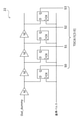
- FIG. 9 is a circuit diagram showing an example of TDC24.
- the TDC 24 includes, for example, a plurality of delay elements and a plurality of D-FFs. A plurality of delay elements are connected in series, and the output of each is input to the D terminal of D-FF.
- the output from the delay element is connected to the D terminal of each D-FF, and the reference pulse is input to the clock terminal.
- the digitized time information is acquired.
- the time difference between the reference pulse and the output from the dummy pixel 102 is output as a digital value.
- a 4-digit signal [3: 0] is output.
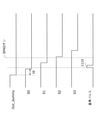
- FIGS. 10 and 11 are diagrams showing an example of the operating waveform of the TDC.
- FIG. 10 shows the case where the SPAD is turned on early with respect to the reference pulse
- FIG. 11 shows the case where the SPAD is turned on slowly with respect to the reference pulse.
- the numerical values described on the timing of the reference pulse are multi-bit signals. For example, in FIG. 10, a signal in which S0, S1, and S2 are 0 and S3 is 1 is input, and in FIG. 11, a signal in which S0 is 0 and S1, S2, and S3 are 1 is input. If it is done.
- the timing of the reference pulse is earlier than the timing of SPAD on, and the synchronization is not achieved.
- the timing of the reference pulse is later than the timing of SPAD on, and the synchronization is not achieved. For this reason, both need to adjust the SPAD on time. For example, when the signal is 1100 and SPAD is turned on, the digital delay circuit 20 delays the signal so that this timing is the same.
- the configuration of the digital delay circuit 20 may be the same as that of the above-described embodiment.
- Dcont a multiplexer that outputs a signal with an appropriate delay when a multi-valued signal is input is provided, and Dcont, which is a multi-valued signal, is input to this multiplexer.
- the phase shift is acquired by the binary value of early or late, whereas in the present embodiment, it is possible to acquire the phase shift by a multi-valued signal. Therefore, for example, when the time is controlled at the timing when the light reception is started, according to the configuration using the TDC of the present embodiment, it is possible to realize the synchronization with the reference pulse at a higher speed than each of the above-described embodiments. It becomes.
- FIG. 12 is a diagram showing another embodiment of the APD sensor 1 according to the present embodiment.
- the output from the effective pixel 100 may be input to the TDC 24 via the ADC (Analog to Digital Converter). This is arranged for distance measurement to acquire the time until reflection after converting the data of the light reflected from the subject into digital data by using the digital data.
- ADC Analog to Digital Converter
- the output of the TDC 24 may be used as a signal for delay control.
- the TDC 24 provided for each dummy pixel 102 for example, provided for each line of the pixel array 10
- the TDC 24 for distance measurement can be replaced with the TDC 24 for distance measurement.
- the number of TDCs can be reduced, so that the circuit area and power consumption can be reduced.
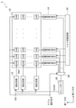
- FIG. 13 is a more detailed drawing of the circuit shown in FIG.
- the column along the first direction and the line along the second direction are provided with 100 effective pixels and 102 dummy pixels in an array.
- Each dummy pixel 102 is connected to the phase comparison circuit 14.
- the output of the phase comparison circuit 14 is input to the multiplexer (hereinafter referred to as MUX26).
- the MUX 26 selects and outputs the input from the phase comparison circuit 14 corresponding to a plurality of columns based on the line selection signal input separately.
- the operation of the charge pump 18 and the delay circuit 12 is the same as that of the above-described embodiment.
- the line is selected by the enable signal Xen and the column is selected by the column selection signal, and the SPAD of the target pixel is synchronized with the reference pulse to turn it on. Then, the pixel having the SPAD turned on receives the light reflected from the subject, and the effective pixel 100 appropriately outputs a signal.
- FIG. 14 is a diagram showing an example of the layout of the APD sensor 1 shown in FIG.
- the APD sensor 1 may be formed on a laminated semiconductor substrate.
- the semiconductor substrate includes a first substrate 30 and a second substrate 32.
- the first substrate 30 and the second substrate 32 are sometimes called dies.
- the first substrate 30 and the second substrate 32 have, for example, a rectangular shape, but the specific shape and size are arbitrary. Further, these substrates may be the same size or different sizes from each other.
- SPAD104 is provided on the first board 30. Further, at least a part of the optical system may be mounted as an on-chip.
- the second board 32 is provided with a pixel reading unit, a delay circuit 12, a phase comparison circuit 14, a pulse generation circuit 16, and a charge pump 18.
- the pixel reading unit includes, for example, a component of the pixel array 10 other than the SPAD, for example, a component other than the SPAD 104 of the effective pixel 100 and the dummy pixel 102.
- the second board 32 is appropriately provided with a power supply circuit, a logic circuit, a storage circuit, an ADC, a DAC (Digital to Analog Converter), etc. necessary for driving the APD sensor 1. It also has an output interface that outputs the signal output from the SPAD.
- the first substrate 30 and the second substrate 32 may be laminated by, for example, a CoC (Chip on Chip) method in which each is cut out from a wafer, separated into individual pieces, and then vertically laminated and laminated. Further, one of the first substrate 30 and the second substrate 32 may be cut out from the wafer and individualized, and then the individualized pieces may be laminated by a CoW (Chip on Wafer) method of bonding to the other substrate. Alternatively, both the first substrate 30 and the second substrate 32 may be laminated by a WoW (Wafer on Wafer) method in which both are bonded in a wafer state.
- a CoC Chip on Chip
- the first substrate 30 and the second substrate 32 may be joined by using various joining methods. For example, plasma junction or the like can be used.
- the first board 30 and the second board 32 may be electrically connected by a micro bump, a micro pad, or the like. Further, it may be electrically connected by a via hole, a contact or the like.
- the effective pixel 100 and the dummy pixel 102 may be provided in the electronic device 1 as the pixel array 10. Further, the circuit such as the pixel array 10 may be formed on a laminated semiconductor substrate.
- FIG. 15 is a diagram showing a configuration example of the effective pixel 100.
- the dummy pixel 102 was an example in which the anode of the SPAD 104 was grounded, but in the effective pixel, the anode of the SPAD 104 is connected to the negative potential -Vbd.
- the potential By setting the potential to a negative potential in this way, when a photon is received, avalanche amplification is generated due to the difference in voltage from the cathode side, and a signal having an appropriate intensity is output even with one photon.
- the effective pixel 100 and the dummy pixel 102 are collectively referred to as a light receiving pixel.
- the figure shows that the anode of the SPAD 104 is connected to a negative potential, but the present invention is not limited to this, and for example, in the case of the dummy pixel 102, it may be a ground potential.
- FIG. 16 is a diagram showing another configuration example of the light receiving pixel.
- the light receiving pixel may further include a pMOS 112 with respect to the nMOS 108. By providing the pMOS 112 in this way, the current source for recharging can be disconnected when the SPAD 104 is on.
- the input of the inverter provided in the pixel becomes floating, and it is possible to suppress the output of the through current.
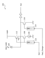
- FIG. 17 is a diagram showing another configuration example of the light receiving pixel.
- the light receiving pixel has a configuration including a shift circuit 114 for high-speed recharging and a pMOS 116 in addition to the configuration shown in FIG.
- the drive voltage (change from High to Low) of pMOS116 is applied from Fast_Charge after the Xen signal.
- pMOS116 is turned on, the speed at which Vca is charged can be improved.
- FIG. 18 is a timing chart of the circuit of FIG. If you change Fast_Charge from High ⁇ Low ⁇ High at the right time, the charge of Vca will be boosted.
- the dotted line shows the voltage transition when there is no Fast_Charge, but by equipping it with pMOS116 and driving it appropriately, it is possible to shorten the time until SPAD104 is turned on.
- FIG. 19 is a diagram showing another configuration example of the light receiving pixel.
- the SPAD 104 may have a configuration in which the cathode is connected to Vbd + Vddh and the anode is Vca.
- the nMOS 108 can turn off the SPAD 104 by disconnecting the recharge current source 106.
- FIG. 20 is a diagram showing another configuration example of the light receiving pixel.
- the SPAD 104 connected as shown in FIG. 19 is recharged with the connected nMOS 108 and pMOS 112 in the same manner as in FIG. Similar to FIG. 16, the input of the inverter becomes floating, and it is possible to suppress the flow of through current.
- FIG. 21 is a diagram showing another configuration example of the light receiving pixel.
- the SPAD 104 connected as shown in FIG. 19 is configured to be recharged at high speed by the connected nMOS 108, pMOS 112, and nMOS 118 as in FIG. 17.
- the voltage of Fast_Chage can be turned on by fighting Low ⁇ High ⁇ Log, and the potential of Vca can be lowered to the ground potential (reference voltage) at high speed.
- SPAD is used as a light receiving element of a pixel, but the present invention is not limited to this.
- the light receiving element may be an APD other than SPAD. That is, all the parts described as SPAD in the above may be read as APD.
- FIG. 22 is a diagram showing a distance measuring system 3 showing a usage example of the APD sensor 1 according to each of the above-described embodiments.
- the distance measuring system 3 includes an APD sensor 1 and a light emitting element 2.
- the APD sensor 1 is a circuit having the configuration described in each of the above-described embodiments.
- the light emission trigger signal may be oscillated by the APD sensor 1 or may be oscillated externally.
- the light emitting element 2 is an element that emits light based on a light emitting trigger signal, and is, for example, an LD (Laser Diode).
- the light emitting element 2 irradiates the target with a laser, and the light receiving element of the APD sensor 1 receives the reflected light from the target.
- LD Laser Diode
- the APD sensor 1 measures the distance between the distance measuring system 3 and the target based on the difference between the time when the light emitting trigger signal is oscillated and the time when the light receiving element receives the light.
- the technology related to this disclosure can be applied to various products.
- the technology according to the present disclosure is any kind of movement such as an automobile, an electric vehicle, a hybrid electric vehicle, a motorcycle, a bicycle, a personal mobility, an airplane, a drone, a ship, a robot, a construction machine, and an agricultural machine (tractor). It may be realized as a device mounted on the body.
- FIG. 23 is a block diagram showing a schematic configuration example of a vehicle control system 7000, which is an example of a mobile control system to which the technique according to the present disclosure can be applied.
- the vehicle control system 7000 includes a plurality of electronic control units connected via a communication network 7010.
- the vehicle control system 7000 includes a drive system control unit 7100, a body system control unit 7200, a battery control unit 7300, an outside information detection unit 7400, an in-vehicle information detection unit 7500, and an integrated control unit 7600. ..
- the communication network 7010 connecting these multiple control units conforms to any standard such as CAN (Controller Area Network), LIN (Local Interconnect Network), LAN (Local Area Network) or FlexRay (registered trademark). It may be an in-vehicle communication network.
- CAN Controller Area Network
- LIN Local Interconnect Network
- LAN Local Area Network
- FlexRay registered trademark
- Each control unit includes a microcomputer that performs arithmetic processing according to various programs, a storage unit that stores programs executed by the microcomputer or parameters used for various arithmetic, and a drive circuit that drives various controlled devices. To prepare for.
- Each control unit is provided with a network I / F for communicating with other control units via the communication network 7010, and is connected to devices or sensors inside or outside the vehicle by wired communication or wireless communication.
- a communication I / F for performing communication is provided. In FIG.
- control unit 7600 As the functional configuration of the integrated control unit 7600, the microcomputer 7610, the general-purpose communication I / F7620, the dedicated communication I / F7630, the positioning unit 7640, the beacon receiving unit 7650, the in-vehicle device I / F7660, the audio image output unit 7670, The vehicle-mounted network I / F 7680 and the storage unit 7690 are illustrated.
- Other control units also include a microcomputer, a communication I / F, a storage unit, and the like.
- the drive system control unit 7100 controls the operation of the device related to the drive system of the vehicle according to various programs.
- the drive system control unit 7100 has a driving force generator for generating the driving force of the vehicle such as an internal combustion engine or a driving motor, a driving force transmission mechanism for transmitting the driving force to the wheels, and a steering angle of the vehicle. It functions as a control device such as a steering mechanism for adjusting and a braking device for generating braking force of the vehicle.
- the drive system control unit 7100 may have a function as a control device such as ABS (Antilock Brake System) or ESC (Electronic Stability Control).
- the vehicle state detection unit 7110 is connected to the drive system control unit 7100.
- the vehicle state detection unit 7110 may include, for example, a gyro sensor that detects the angular velocity of the axial rotation motion of the vehicle body, an acceleration sensor that detects the acceleration of the vehicle, an accelerator pedal operation amount, a brake pedal operation amount, or steering wheel steering. It includes at least one of sensors for detecting an angle, engine speed, wheel speed, and the like.
- the drive system control unit 7100 performs arithmetic processing using a signal input from the vehicle state detection unit 7110, and controls an internal combustion engine, a drive motor, an electric power steering device, a brake device, and the like.
- the body system control unit 7200 controls the operation of various devices mounted on the vehicle body according to various programs.
- the body system control unit 7200 functions as a keyless entry system, a smart key system, a power window device, or a control device for various lamps such as headlamps, back lamps, brake lamps, turn signals or fog lamps.
- a radio wave transmitted from a portable device that substitutes for a key or signals of various switches may be input to the body system control unit 7200.
- the body system control unit 7200 receives inputs of these radio waves or signals and controls a vehicle door lock device, a power window device, a lamp, and the like.
- the battery control unit 7300 controls the secondary battery 7310, which is the power supply source of the drive motor, according to various programs. For example, information such as the battery temperature, the battery output voltage, or the remaining capacity of the battery is input to the battery control unit 7300 from the battery device including the secondary battery 7310. The battery control unit 7300 performs arithmetic processing using these signals, and controls the temperature control of the secondary battery 7310 or the cooling device provided in the battery device.
- the vehicle outside information detection unit 7400 detects information outside the vehicle equipped with the vehicle control system 7000.
- the image pickup unit 7410 and the vehicle exterior information detection unit 7420 is connected to the vehicle exterior information detection unit 7400.
- the image pickup unit 7410 includes at least one of a ToF (Time Of Flight) camera, a stereo camera, a monocular camera, an infrared camera, and other cameras.
- the vehicle outside information detection unit 7420 is used, for example, to detect the current weather or an environment sensor for detecting the weather, or other vehicles, obstacles, pedestrians, etc. around the vehicle equipped with the vehicle control system 7000. At least one of the surrounding information detection sensors is included.
- the environment sensor may be, for example, at least one of a raindrop sensor that detects rainy weather, a fog sensor that detects fog, a sunshine sensor that detects the degree of sunshine, and a snow sensor that detects snowfall.
- the ambient information detection sensor may be at least one of an ultrasonic sensor, a radar device, and a LIDAR (Light Detection and Ranging, Laser Imaging Detection and Ranging) device.
- the image pickup unit 7410 and the vehicle exterior information detection unit 7420 may be provided as independent sensors or devices, or may be provided as a device in which a plurality of sensors or devices are integrated.
- FIG. 24 shows an example of the installation position of the image pickup unit 7410 and the vehicle outside information detection unit 7420.
- the image pickup unit 7910, 7912, 7914, 7916, 7918 are provided, for example, at at least one of the front nose, side mirror, rear bumper, back door, and upper part of the windshield of the vehicle interior of the vehicle 7900.
- the image pickup unit 7910 provided in the front nose and the image pickup section 7918 provided in the upper part of the windshield in the vehicle interior mainly acquire an image in front of the vehicle 7900.
- the image pickup units 7912 and 7914 provided in the side mirrors mainly acquire images of the side of the vehicle 7900.
- the image pickup unit 7916 provided in the rear bumper or the back door mainly acquires an image of the rear of the vehicle 7900.
- the image pickup unit 7918 provided on the upper part of the windshield in the vehicle interior is mainly used for detecting a preceding vehicle, a pedestrian, an obstacle, a traffic light, a traffic sign, a lane, or the like.
- FIG. 24 shows an example of the shooting range of each of the imaging units 7910, 7912, 7914, 7916.
- the imaging range a indicates the imaging range of the imaging unit 7910 provided on the front nose
- the imaging ranges b and c indicate the imaging range of the imaging units 7912 and 7914 provided on the side mirrors, respectively
- the imaging range d indicates the imaging range d.
- the imaging range of the imaging unit 7916 provided on the rear bumper or the back door is shown. For example, by superimposing the image data captured by the image pickup units 7910, 7912, 7914, 7916, a bird's-eye view image of the vehicle 7900 can be obtained.
- the vehicle exterior information detection unit 7920, 7922, 7924, 7926, 7928, 7930 provided on the front, rear, side, corner and the upper part of the windshield in the vehicle interior of the vehicle 7900 may be, for example, an ultrasonic sensor or a radar device.
- the vehicle exterior information detection units 7920, 7926, 7930 provided on the front nose, rear bumper, back door, and upper part of the windshield in the vehicle interior of the vehicle 7900 may be, for example, a lidar device.
- These out-of-vehicle information detection units 7920 to 7930 are mainly used for detecting a preceding vehicle, a pedestrian, an obstacle, or the like.
- the vehicle outside information detection unit 7400 causes the image pickup unit 7410 to capture an image of the outside of the vehicle and receives the captured image data. Further, the vehicle outside information detection unit 7400 receives detection information from the connected vehicle outside information detection unit 7420.
- the vehicle exterior information detection unit 7420 is an ultrasonic sensor, a radar device, or a lidar device
- the vehicle exterior information detection unit 7400 transmits ultrasonic waves, electromagnetic waves, or the like, and receives received reflected wave information.
- the out-of-vehicle information detection unit 7400 may perform object detection processing or distance detection processing such as a person, a vehicle, an obstacle, a sign, or a character on a road surface based on the received information.
- the out-of-vehicle information detection unit 7400 may perform an environment recognition process for recognizing rainfall, fog, road surface conditions, etc. based on the received information.
- the out-of-vehicle information detection unit 7400 may calculate the distance to an object outside the vehicle based on the received information.
- the vehicle outside information detection unit 7400 may perform image recognition processing or distance detection processing for recognizing a person, a vehicle, an obstacle, a sign, a character on the road surface, or the like based on the received image data.
- the vehicle outside information detection unit 7400 performs processing such as distortion correction or alignment on the received image data, and synthesizes image data captured by different image pickup units 7410 to generate a bird's-eye view image or a panoramic image. May be good.
- the vehicle exterior information detection unit 7400 may perform the viewpoint conversion process using the image data captured by different image pickup units 7410.
- the in-vehicle information detection unit 7500 detects the in-vehicle information.
- a driver state detection unit 7510 that detects the state of the driver is connected to the in-vehicle information detection unit 7500.
- the driver state detection unit 7510 may include a camera that captures the driver, a biosensor that detects the driver's biological information, a microphone that collects sound in the vehicle interior, and the like.
- the biosensor is provided on, for example, a seat surface or a steering wheel, and detects biometric information of a passenger sitting on the seat or a driver holding the steering wheel.
- the in-vehicle information detection unit 7500 may calculate the degree of fatigue or concentration of the driver based on the detection information input from the driver state detection unit 7510, and may determine whether the driver is asleep. You may.
- the in-vehicle information detection unit 7500 may perform processing such as noise canceling processing on the collected audio signal.
- the integrated control unit 7600 controls the overall operation in the vehicle control system 7000 according to various programs.
- An input unit 7800 is connected to the integrated control unit 7600.
- the input unit 7800 is realized by a device that can be input-operated by the passenger, such as a touch panel, a button, a microphone, a switch, or a lever. Data obtained by recognizing the voice input by the microphone may be input to the integrated control unit 7600.
- the input unit 7800 may be, for example, a remote control device using infrared rays or other radio waves, or an external connection device such as a mobile phone or a PDA (Personal Digital Assistant) corresponding to the operation of the vehicle control system 7000. You may.
- the input unit 7800 may be, for example, a camera, in which case the passenger can input information by gesture. Alternatively, data obtained by detecting the movement of the wearable device worn by the passenger may be input. Further, the input unit 7800 may include, for example, an input control circuit that generates an input signal based on the information input by the passenger or the like using the input unit 7800 and outputs the input signal to the integrated control unit 7600. By operating the input unit 7800, the passenger or the like inputs various data to the vehicle control system 7000 and instructs the processing operation.
- the storage unit 7690 may include a ROM (Read Only Memory) for storing various programs executed by the microcomputer, and a RAM (Random Access Memory) for storing various parameters, calculation results, sensor values, and the like. Further, the storage unit 7690 may be realized by a magnetic storage device such as an HDD (Hard Disc Drive), a semiconductor storage device, an optical storage device, an optical magnetic storage device, or the like.
- ROM Read Only Memory
- RAM Random Access Memory
- the general-purpose communication I / F 7620 is a general-purpose communication I / F that mediates communication with various devices existing in the external environment 7750.
- General-purpose communication I / F7620 is a cellular communication protocol such as GSM (registered trademark) (Global System of Mobile communications), WiMAX (registered trademark), LTE (registered trademark) (Long Term Evolution) or LTE-A (LTE-Advanced).
- GSM Global System of Mobile communications
- WiMAX registered trademark
- LTE registered trademark
- LTE-A Long Term Evolution-Advanced
- Bluetooth® may be implemented.
- the general-purpose communication I / F7620 connects to a device (for example, an application server or a control server) existing on an external network (for example, the Internet, a cloud network, or a business-specific network) via a base station or an access point, for example. You may. Further, the general-purpose communication I / F7620 uses, for example, P2P (Peer To Peer) technology, and is a terminal existing in the vicinity of the vehicle (for example, a driver, a pedestrian or a store terminal, or an MTC (Machine Type Communication) terminal). May be connected with.
- P2P Peer To Peer
- MTC Machine Type Communication
- the dedicated communication I / F 7630 is a communication I / F that supports a communication protocol formulated for use in a vehicle.
- the dedicated communication I / F7630 uses a standard protocol such as WAVE (Wireless Access in Vehicle Environment), DSRC (Dedicated Short Range Communications), which is a combination of the lower layer IEEE802.11p and the upper layer IEEE1609, or a cellular communication protocol. May be implemented.
- Dedicated communication I / F7630 is typically vehicle-to-vehicle (Vehicle to Vehicle) communication, road-to-vehicle (Vehicle to Infrastructure) communication, vehicle-to-house (Vehicle to Home) communication, and pedestrian-to-vehicle (Vehicle to Pedestrian) communication. ) Carry out V2X communication, a concept that includes one or more of the communications.
- the positioning unit 7640 receives, for example, a GNSS signal from a GNSS (Global Navigation Satellite System) satellite (for example, a GPS signal from a GPS (Global Positioning System) satellite), executes positioning, and executes positioning, and the latitude, longitude, and altitude of the vehicle. Generate location information including.
- the positioning unit 7640 may specify the current position by exchanging signals with the wireless access point, or may acquire position information from a terminal such as a mobile phone, PHS, or smartphone having a positioning function.
- the beacon receiving unit 7650 receives radio waves or electromagnetic waves transmitted from a radio station or the like installed on the road, and acquires information such as the current position, traffic jam, road closure, or required time.
- the function of the beacon receiving unit 7650 may be included in the above-mentioned dedicated communication I / F 7630.
- the in-vehicle device I / F 7660 is a communication interface that mediates the connection between the microcomputer 7610 and various in-vehicle devices 7760 existing in the vehicle.
- the in-vehicle device I / F7660 may establish a wireless connection using a wireless communication protocol such as wireless LAN, Bluetooth (registered trademark), NFC (Near Field Communication) or WUSB (Wireless USB).
- a wireless communication protocol such as wireless LAN, Bluetooth (registered trademark), NFC (Near Field Communication) or WUSB (Wireless USB).
- the in-vehicle device I / F7660 is via a connection terminal (and a cable if necessary) (not shown), USB (Universal Serial Bus), HDMI (registered trademark) (High-Definition Multimedia Interface, or MHL (Mobile High)).
- -Definition Link and other wired connections may be established.
- the in-vehicle device 7760 includes, for example, at least one of a passenger's mobile device or wearable device, or an information device carried in or attached to the vehicle. Further, the in-vehicle device 7760 may include a navigation device for searching a route to an arbitrary destination.
- the in-vehicle device I / F 7660 may be a control signal to and from these in-vehicle devices 7760. Or exchange the data signal.
- the in-vehicle network I / F7680 is an interface that mediates communication between the microcomputer 7610 and the communication network 7010.
- the vehicle-mounted network I / F7680 transmits / receives signals and the like according to a predetermined protocol supported by the communication network 7010.
- the microcomputer 7610 of the integrated control unit 7600 is via at least one of general-purpose communication I / F7620, dedicated communication I / F7630, positioning unit 7640, beacon receiving unit 7650, in-vehicle device I / F7660, and in-vehicle network I / F7680.
- the vehicle control system 7000 is controlled according to various programs based on the information acquired. For example, the microcomputer 7610 calculates the control target value of the driving force generator, the steering mechanism, or the braking device based on the acquired information inside and outside the vehicle, and outputs a control command to the drive system control unit 7100. May be good.
- the microcomputer 7610 realizes ADAS (Advanced Driver Assistance System) functions including vehicle collision avoidance or impact mitigation, follow-up driving based on inter-vehicle distance, vehicle speed maintenance driving, vehicle collision warning, vehicle lane deviation warning, and the like. Cooperative control may be performed for the purpose of.
- the microcomputer 7610 automatically travels autonomously without relying on the driver's operation by controlling the driving force generator, steering mechanism, braking device, etc. based on the acquired information on the surroundings of the vehicle. Coordinated control may be performed for the purpose of driving or the like.
- the microcomputer 7610 has information acquired via at least one of a general-purpose communication I / F7620, a dedicated communication I / F7630, a positioning unit 7640, a beacon receiving unit 7650, an in-vehicle device I / F7660, and an in-vehicle network I / F7680. Based on the above, three-dimensional distance information between the vehicle and an object such as a surrounding structure or a person may be generated, and local map information including the peripheral information of the current position of the vehicle may be created. Further, the microcomputer 7610 may predict the danger of a vehicle collision, a pedestrian or the like approaching or entering a closed road, and generate a warning signal based on the acquired information.
- the warning signal may be, for example, a signal for generating a warning sound or lighting a warning lamp.
- the audio image output unit 7670 transmits an output signal of at least one of audio and image to an output device capable of visually or audibly notifying information to the passenger or the outside of the vehicle.
- an audio speaker 7710, a display unit 7720, and an instrument panel 7730 are exemplified as output devices.
- the display unit 7720 may include, for example, at least one of an onboard display and a head-up display.
- the display unit 7720 may have an AR (Augmented Reality) display function.
- the output device may be other devices such as headphones, wearable devices such as eyeglass-type displays worn by passengers, projectors or lamps other than these devices.
- the display device displays the results obtained by various processes performed by the microcomputer 7610 or the information received from other control units in various formats such as texts, images, tables, and graphs. Display visually.
- the audio output device converts an audio signal composed of reproduced audio data, acoustic data, or the like into an analog signal and outputs it audibly.
- At least two control units connected via the communication network 7010 may be integrated as one control unit.
- each control unit may be composed of a plurality of control units.
- the vehicle control system 7000 may include another control unit (not shown).
- the other control unit may have a part or all of the functions carried out by any of the control units. That is, as long as information is transmitted and received via the communication network 7010, predetermined arithmetic processing may be performed by any of the control units.
- a sensor or device connected to any control unit may be connected to another control unit, and a plurality of control units may send and receive detection information to and from each other via the communication network 7010. .
- the first pixel which has an APD as a light receiving element and is used for light receiving
- a second pixel that has an APD as a light receiving element and is not used for light receiving
- a phase comparison circuit in which an output of at least one of the first pixel or the second pixel and a reference pulse signal are input, and the phase difference between the one output and the reference pulse is output.
- the delay circuit delays the enable signal to synchronize the reference pulse with the timing at which the voltage that enables the output of the light receiving element in the first pixel is charged.
- the delay circuit delays the enable signal, which charges the anode or cathode of the APD with a voltage for driving a light receiving state.
- the APD sensor described in (2) The APD sensor described in (2).
- the phase comparison circuit is The D-FF is provided, wherein the output of the first pixel or the second pixel is input to the D terminal, the reference pulse signal is input to the clock terminal, and the output is output from the Q terminal.
- the APD sensor according to any one of (1) to (3).
- the delay circuit When the output of the phase comparison circuit is low, the delay circuit outputs the enable signal with a longer delay as compared with the case where the output of the phase comparison circuit is high.
- the phase comparison circuit is a TDC that converts the time difference between the output of at least one of the first pixel or the second pixel and the reference pulse signal into a multi-bit digital signal.
- the APD sensor according to any one of (1) to (3).
- the first pixel is provided in an array in a second direction which is a direction intersecting the first direction and the first direction, and the second pixel is provided in a plurality of the first pixels provided along the first direction.
- Pixel array with at least one The APD sensor according to any one of (1) to (6), further comprising.
- the second pixel is provided in the pixel array in a wiring closer to the phase comparison circuit than the first pixel along each of the first directions.
- the phase comparison circuit compares the phase of the output of the second pixel with the reference pulse and outputs the phase.
- the first substrate provided with the APD and A second substrate having at least the phase comparison circuit and the delay circuit, and formed by laminating the first substrate.
- a semiconductor substrate comprising The APD sensor according to any one of (1) to (8).
- the APD sensor according to any one of (1) to (9) and Light emitting element and Equipped with The light emitted from the light emitting element receives the light reflected by the subject at the first pixel, and the subject reaches the subject based on the timing at which the light emitting element emits the light and the timing at which the first pixel receives the light. Measure the distance, Distance measurement system.
- the aspect of the present disclosure is not limited to the above-mentioned embodiment, but also includes various possible modifications, and the effect of the present disclosure is not limited to the above-mentioned contents.
- the components in each embodiment may be applied in appropriate combinations. That is, various additions, changes and partial deletions are possible without departing from the conceptual idea and purpose of the present disclosure derived from the contents specified in the claims and their equivalents.
- APD sensor 10: Pixel array, 100: Effective pixel, 102: Dummy pixel, 104: SPAD, 106: current source, 108: n MOSFET, 110: shift circuit, 12: Delay circuit, 14: Phase comparison circuit, 16: Pulse oscillation circuit, 18: Charge pump, 20: Digital delay circuit, 22: Control logic circuit, 24: TDC, 26: MUX, 30: 1st board, 32: 2nd board, 2: Light emitting element, 3: Distance measurement system
Landscapes
- Physics & Mathematics (AREA)
- Engineering & Computer Science (AREA)
- General Physics & Mathematics (AREA)
- Radar, Positioning & Navigation (AREA)
- Remote Sensing (AREA)
- Computer Networks & Wireless Communication (AREA)
- Electromagnetism (AREA)
- Optical Radar Systems And Details Thereof (AREA)
- Measurement Of Optical Distance (AREA)
Abstract
[課題]SPADの駆動タイミングの精度を向上する。 [解決手段]APDセンサは、第1画素と、第2画素と、位相比較回路と、遅延回路とを備える。第1画素は、受光素子としてAPD(Avalanche Photo Diode)を有し、受光に用いられる。第2画素は、受光素子としてAPDを有し、受光に用いない。位相比較回路は、前記第1画素又は前記第2画素の少なくとも一方の出力と、基準パルス信号が入力され、前記一方の出力と、前記基準パルスとの位相差を出力する。遅延回路は、前記位相比較回路の出力と、イネーブル信号が入力され、遅延されたイネーブル信号を出力する。
Description
本開示は、APDセンサ及び測距システムに関する。
測距手法として、LiDAR(Light Detection and Ranging)が広く用いられ、このLiDARには、今日、SPAD(Single Photon Avalanche Diode)をはじめとするAPD(Avalanche Photo Diode)が用いられることがある。APDは、強い電界を掛けた受光部に光子が衝突することによりアバランシェ増幅を発生させ、この効果により微弱な入射光であっても大きな電位変化を引き起こすことが可能である。特に、SPADは、1光子単位での検出をすることが可能である。一方で、APDは、光を検出した後にリチャージの時間が必要であり、デッドタイムが存在する。このデッドタイム期間において、APDは、次の光子を検出することができない。LiDARに用いる筐体は、その内部に光源と受光素子の両方が備えられることが多い。このため、光源から射出された光が筐体内で反射し、受光素子に入射する迷光が発生することがある。
APDを受光素子として用いている場合、APDにブレークダウン以上の電圧を印加することにより素子をオンさせて光子が検出できる状態とする。この電圧を印加することにより、光子を検出できる状態とすることができるが、このタイミングが早いと、筐体内で反射した光子がAPDに入射し、ターゲットからの反射光を受光する前に光子を検出し、ターゲットからの反射光を受光するタイミングでデッドタイム期間に該当することがある。一方で、この電圧を印加するタイミングが遅いと、ターゲットからの反射光を受光するタイミングにおいては、チャージが終了しておらず、やはり適切にターゲットから反射した光を検出することができない。
また、受光センサ内でのAPDのオン/オフを制御するタイミング制御回路を有する場合、制御回路出力では正確なタイミング制御が可能であるが、画素アレイの制御信号を駆動するドライバの遅延、制御信号を画素駆動電圧に変換するレベルシフタの遅延、APDのリチャージ時間等は、素子のばらつき、温度/電源電圧に依存するため、実際にAPDがオン状態となるタイミングを制御することは困難である。
そこで、本開示では、APDの駆動タイミングの精度を向上するAPDセンサを実現する。
一実施形態によれば、APDセンサは、受光素子としてAPDを有し、受光に用いられる第1画素と、受光素子としてAPDを有し、受光に用いない第2画素と、前記第1画素又は前記第2画素の少なくとも一方の出力と、基準パルス信号が入力され、前記一方の出力と、前記基準パルスとの位相差を出力する、位相比較回路と、前記位相比較回路の出力と、イネーブル信号が入力され、遅延されたイネーブル信号を出力する、遅延回路と、を備える。
前記遅延回路は、前記イネーブル信号を遅延させて、前記基準パルスと、前記第1画素における受光素子の出力を可能とする電圧がチャージされるタイミングと、を同期させてもよい。
前記遅延回路は、前記APDのアノード又はカソードに、受光状態を駆動するための電圧をチャージする前記イネーブル信号を遅延させてもよい。
前記位相比較回路は、前記第1画素又は前記第2画素の出力がD端子に入力され、前記基準パルス信号がクロック端子に入力され、Q端子から出力をする、D-FFを備えてもよい。
前記遅延回路は、前記位相比較回路の出力がLowである場合には、前記位相比較回路の出力がHighである場合と比較して、より長く前記イネーブル信号をさらに遅延させて出力してもよい。
前記位相比較回路は、前記第1画素又は前記第2画素の少なくとも一方の出力と、前記基準パルス信号との時間差を、多ビットのデジタル信号に変換するTDCであってもよい。
前記第1画素を、第1方向及び前記第1方向に交わる方向である第2方向にアレイ状に備え、前記第2画素を、前記第1方向に沿って備えられる複数の前記第1画素に対して少なくとも1つを備える、画素アレイをさらに備えてもよい。
前記第2画素は、前記画素アレイにおいて、それぞれの前記第1方向に沿った前記第1画素よりも、前記位相比較回路と配線的に近くに備えられてもよく、前記位相比較回路は、前記第2画素の出力と、前記基準パルスとの位相を比較して出力してもよい。
前記APDを備える、第1基板と、前記位相比較回路と、前記遅延回路と、を少なくとも備え、前記第1基板と積層して形成される、第2基板と、を備える半導体基板上に形成されてもよい。
一実施形態によれば、測距システムは、前述のAPDセンサと、発光素子と、を備え、前記発光素子から射出した光が被写体において反射した光を、前記第1画素で受光し、前記発光素子が光を射出したタイミングと、前記第1画素が受光したタイミングに基づいて、前記被写体までの距離を測定する。
以下、図面を参照して本開示における実施形態の説明をする。図面は、説明のために用いるものであり、実際の装置における各部の構成の形状、サイズ、又は、他の構成とのサイズの比等が図に示されている通りである必要はない。また、図面は、簡略化して書かれているため、図に書かれている以外にも実装上必要な構成は、適切に備えるものとする。
(第1実施形態)
図1は、一実施形態に係るAPD(Avalanche Photo Diode)センサを模式的に示す回路図である。APDセンサ1は、例えば、画素アレイ10と、遅延回路12と、位相比較回路14と、パルス発振回路16と、を備える。APDセンサ1は、画素アレイ10に備えられる受光素子に入射した光を信号に変換して出力する回路である。
図1は、一実施形態に係るAPD(Avalanche Photo Diode)センサを模式的に示す回路図である。APDセンサ1は、例えば、画素アレイ10と、遅延回路12と、位相比較回路14と、パルス発振回路16と、を備える。APDセンサ1は、画素アレイ10に備えられる受光素子に入射した光を信号に変換して出力する回路である。
なお、この図1においては、受光に関しての制御について示されており、信号の出力に関しては示されていないが、適切に出力するための回路を備えるものとする。また、遅延回路12から画素アレイ10の各画素への信号線等は、省略されているが、こちらについても適切に備えられるものとする。例えば、遅延回路12からは、図において水平方向(ライン方向)に信号が順番に与えられてもよい。
画素アレイ10は、有効画素100(第1画素)と、ダミー画素102(第2画素)と、を第1方向及び第2方向に沿ったアレイ状に備える。有効画素100と、ダミー画素102は、それぞれ複数備えられる。図に示すように、画素アレイ10は、例えば、有効画素100よりも位相比較回路14に近い領域にダミー画素102を備える。
有効画素100は、受光を受け付ける画素であり、この有効画素100において受光すると、この光を信号へと変換して出力する。有効画素100は、例えば、SPAD(Single Photon Avalanche Diode)を備えて構成される。
ダミー画素102は、受光を受け付けない画素であり、タイミング制御に用いられる画素である。ダミー画素102も基本的には有効画素100と同じSPADを備えて構成されるが、例えば、受光ができない、又は、受光した光を信号に変換しないように配置される。例えば、ダミー画素102は、SPADの受光面を遮光され、又は、SPADのアノードを接地電位に接続されて配置される。
ダミー画素102は、遅延回路12からの制御により開放されたSPADの電子がチャージされたタイミングで位相比較回路14に信号を出力する。ダミー回路102の状態に基づいて遅延回路12の制御信号を遅延させるので、ダミー回路102と位相比較回路14との距離を近くして、遅延を少なくすることが望ましい。例えば、図1のような構造の場合、ダミー回路102は、第1方向に沿って、有効画素100よりも位相比較回路14に近い位置に配置されることが望ましい。
遅延回路12は、画素アレイ10に備えられる有効画素100及びダミー画素102の受光制御をする信号を出力する回路である。例えば、遅延回路12からは、各第2方向に並ぶ有効画素100及びダミー画素102を制御する信号がラインごとに出力される。有効画素100及びダミー画素102は、ラインごとに遅延回路12から出力される制御信号に基づいて、受光を開始し、受光した場合には、SPADにおいて光を信号へと変換し、適切に出力する。
位相比較回路14は、ダミー回路102から出力された信号と、パルス発振回路16から受信した信号との位相差を比較して出力する。
遅延回路12は、位相比較回路14が出力した位相差に基づいて、制御信号を遅延させて画素へと出力する。この遅延された制御信号に基づいて、適切なタイミングで各画素のSPADを受光状態とすることにより、迷光による信号の出力を回避したタイミングで各画素における受光を適切に実現する。
なお、位相比較回路14は、1つの回路として示されているが、それぞれのダミー画素102ごと、又は、それぞれのカラムごとに備えられていてもよい。例えば、1カラムに対して、1つのダミー画素102が備えられ、このダミー画素102に対して、それぞれ位相比較回路14が備えられてもよい。もちろん、この構成には限られず、適切に以下に説明する動作が実行できるものであればよい。
図2は、本実施形態に係るダミー画素102の接続の一例を示す図である。なお、この図2においては、適切に電圧が調整される回路、例えば、バッファ回路等が備えられてもよい。例えば、遅延回路12と有効画素100、ダミー画素102との間には、バッファ回路が備えられてもよい。
ダミー画素102は、チャージが終了すると、当該信号をダミー信号Out_dummyとして出力する。この信号は、位相比較回路14に入力される。
位相比較回路14には、このダミー信号と、パルス発振回路16から出力された基準パルスとが入力される。位相比較回路14は、パルス信号に対するダミー信号の遅延を位相差として出力する。
チャージポンプ18は、この位相差信号に基づいて電圧を増減させて出力する。チャージポンプ18は、例えば、位相比較回路14の出力がHigh(オン)である場合には、Vcontを高くし、逆に、位相比較回路14の出力がLow(オフ)である場合には、Vcontを低くして出力する。この電圧の制御は、例えば、クロック信号が入力されるタイミングにおいて位相比較回路14の出力がHighであるか、Lowであるかにより、実行される。
チャージポンプ18は、位相比較回路14内に備えられてもよく、また、位相比較回路14の出力する信号が、オン/オフのタイミングにおいてVcontに十分な電位差を生じさせる場合には、備えられなくてもよい。
遅延回路12は、位相比較回路14が出力した位相差信号に基づいて、制御信号Xinを遅延した信号Xenをそれぞれの画素へと出力する。出力は、前述したように、例えばラインごとの信号としての制御電圧である。
ダミー画素102は、例えば、SPAD 104と、電流源106と、n型のMOSFET(Metal-Oxide-Semiconductor Field-Effect-Transistor、以下、nMOS 108と記載する)と、シフト回路110と、を備える。この構成は、基本的には有効画素100においても同様である。上述したように、ダミー画素102においては、例えば、SPAD 104の受光面が遮光され、受光による画素信号を出力しないように設定される。
電流源106は、例えば、電源電圧Vddhと接続され、SPAD 104のカソード側のキャリアをチャージする。このチャージにより、放電後のSPAD 104が受光可能な状態へと遷移する。
nMOS 108は、SPAD 104から信号が出力された後に、SPAD 104のカソードを放電するためのスイッチであり、所定のタイミングにおいてオン/オフされ、SPAD 104のカソード側の充放電を制御する。このnMOS 108の制御をする駆動信号を遅延回路12が出力する。
シフト回路110は、遅延回路12が出力した電圧の基準レベルをnMOS 108の電圧の基準レベルへと変化させる回路である。このシフト回路110には、一般的に用いられるレベルシフト回路を適切に用いることができる。
ダミー画素102は、遅延回路12から制御信号がオンされたタイミングでSPAD 104のカソード側の電圧Vcaを基準電圧(例えば、接地電位)まで放電する。そして、遅延回路12からの制御信号がオフされたタイミングで電圧Vcaを所定電圧までチャージする。
ダミー画素102は、バッファにより、電圧Vcaが所定電圧を超えると、信号を出力する。この所定の電圧は、SPAD 104が起動するためにカソード側に印加される電圧である。
位相比較回路14は、ダミー画素102から信号が出力されると、基準パルスとの位相差を出力する。遅延回路12は、この位相差に基づいて制御信号Xenを、例えば、ToF(Time of Flight)センサにおけるレーザーの発光タイミングからの遅延を調整して出力する。
図3は、本実施形態に係るタイミングチャートを模式的に示す図である。最上段の発光トリガは、ToFセンサにおけるレーザーの照射タイミングを示すトリガ信号である。この発光トリガに基づいて、レーザーが被写体へと照射される。
Xenは、画素からの出力を制御する制御信号である。このXenから発光トリガまでの時間をtd_LDとする。
Vcaは、SPAD 104のカソード側の電圧である。制御信号Xenがオフになった後にSPAD 104が受光可能状態になるまでの時間をtd_wakeupとする。制御信号Xenが入力された後に、td_wakeup時間経過すると、SPAD 104が受光可能な状態となる。
図3に示すようなタイミングでSPAD 104がオンすることにより、被写体から反射したフォトンを適切にSPAD 104が受光することが可能となる。
SPADがオンとなるタイミングが早い場合、例えば、td_LDがtd_wakeupと同等の時間である場合には、SPADがオンした後に、筐体内反射によるフォトンをSPAD 104が受光し、その後とのSPADがデッドタイムとなったタイミングで被写体からの反射光を受光する。このようなタイミングであると、筐体内の反射光による信号を出力し、被写体からの反射光を適切に受光することができない。このため、正しい距離を測定することができない。
一方で、SPADがオンとなるタイミングが遅い場合、すなわち、td_wakeupの間に被写体の反射項がSPADに到達してしまう場合、SPADにおける被写体から反射したフォトンの雪崩増幅を適切に発生させることができない。このため、この場合も、被写体との正しい距離を測定することができない。
上記から、図3に示すように、適切なタイミングで制御信号Xenを切り替えて、被写体からの反射光をSPAD 104に受光させる必要がある。そこで、図2において説明したように、ダミー画素102におけるチャージが終わる時間(td_wakeup)に基づいてXenを遅延させる制御を実行する。
位相比較回路14は、上記に示したように制御信号Xenを出力するため、例えば、D-FF(D-Flip Flop)を備える。例えば、D-FFのD端子にダミー画素102の出力を接続し、クロック端子に基準パルスを入力する。
SPADがオンとなるタイミングが基準パルスよりも早い場合、位相比較回路14の出力は、基準パルスが入力されたタイミングでダミー画素102からの出力はオフであるため、Lowとなる。
一方で、SPADがオンとなるタイミングが基準パルスよりも遅い場合、位相比較回路14の出力は、基準パルスが入力されたタイミングでダミー画素102からの出力はオンであるため、Highとなる。
位相比較回路14の出力は、チャージポンプ18に入力され、昇圧される。なお、High、Lowのパルス信号に応じて出力する電圧が適切に制御できる回路であれば、チャージポンプの代わりに用いることができる。位相比較回路14又はチャージポンプ18からは、電圧Vcontが遅延回路12へと出力される。
図4は、本実施形態に係る遅延回路12を模式的に示す回路図である。
遅延回路12は、偶数個のインバータを直列に接続した回路である。インバータの入力には、イネーブル信号であるXinが入力され、最後のインバータからは、遅延されたイネーブル信号であるXenが出力される。このXenが有効画素100及びダミー画素102へと出力される。より詳しくは、図1に示すように、ラインに沿った画素に対する信号として出力される。図は、一例として示すものであり、遅延回路12が備えるインバータの数は、オンオフが反転しない任意の数として構わない。
それぞれのインバータは、電源電圧として、VddとVssに接続される。インバータとVssとの間に、例えば、ゲートに電圧Vcontが接続されるnMOSが接続される。電圧Vcontが高いと、インバータに流れる電流が多くなるため、遅延時間は短くなる。一方で、電圧Vcontが低いと、インバータに流れる電流が少なくなるため、遅延時間が長くなる。
これらをまとめると、ダミー画素102において、SPADの受光可能期間への立ち上がりが発光に対して早い場合には、移動比較回路14の出力がLow、すなわち、電圧Vcontが低くなり、Xinに対するXenの遅延が長くなる。このため、ダミー画素102のSPAD 104の受光可能期間の立ち上がり時間を現状よりも遅らせる。
一方で、ダミー画素102において、SPADの受光可能期間への立ち上がりが発光に対して遅い場合には、移動比較回路14の出力がHigh、すなわち、電圧Vcontが高くなり、Xinに対するXenの遅延が短くなる。このため、ダミー画素102のSPAD 104の受光可能期間の立ち上がり時間を現状よりも早くさせる。
このように、制御回路12、ダミー画素102、位相比較回路14、チャージポンプ18により、DLL(Delay Locked Loop)を形成する。APDセンサ1は、このDLLにより、SPADのオンタイミングを調整する。
各回路素子は、上記のイネーブル信号の出力の遅延が図3の状態となる回路定数となるように適切に選択される。適切に構成されたDLLを用いることにより、基準パルスと同期したタイミングでSPADをオンすることが可能となり、素子のばらつき、温度、電圧に依存しない既知のタイミングでSPADをオンすることができる。
以上のように、本実施形態によれば、画素におけるSPAD 104の受光可能期間を適切に設定することが可能となり、迷光等の影響を回避することが可能となる。図1に示すように、ダミー画素102と位相比較回路14の配線を、有効画素100よりも短くすることにより、ダミー画素102から位相比較回路14への信号の配線における遅延を抑制することが可能である。このため、画素におけるSPADの立ち上げ時間をより正確にイネーブル信号へと反映させることができる。
また、カラムごとにダミー画素102を備えることにより、カラムごとの遅延をダミー画素102において適切に検出することができる。このため、制御回路12から遅延された背イネーブル信号Xenをラインごとに出力した場合に、ラインに沿った画素に対して、配線の遅延を適切に反映することが可能となる。
なお、画素アレイ10に画素が備えられている場合について説明したが、この遅延制御は、画素アレイ10ではなく、さらに細かい一般的な受光画素に用いることが可能である。すなわち、図2の構成は、図1の構成だけではなく、単体として用いることも可能である。また、画素アレイ10を制御するための信号についての詳細は、後述する。
図5は、本実施形態に係るAPDセンサ1の別の態様を示す図である。上記では、位相比較回路14との距離が近いダミー回路102の出力を用いるとしたが、これには限られない。有効画素100のうち、位相比較回路までの配線遅延が必要なタイミング調整の精度に比べて小さい画素がある場合には、この有効画素100の出力を信号遅延に用いてもよい。
図5のAPDセンサ1では、有効画素100の配線遅延が少ない画素の出力を用いている。このように、ダミー画素102ではなく、有効画素100の出力を用いて遅延制御を実行してもよい。このように有効画素100を用いることにより、有効画素100自体のオンタイミングを調整することが可能となる。この場合、ダミー画素102はまた、必須の構成ではなく、利用環境、回路設置面積等の制限によりダミー画素102を配置できない、又は、ダミー画素102の配線をする余裕がない場合等にも、同様の効果を得ることができる。
ダミー画素102を備えない場合には、上述したように配線遅延が発生しづらい有効画素100を選択することが望ましい。このため、出力を遅延制御に用いる有効画素100としては、例えば、図1に示す回路と同様に、画素アレイ10において、他の有効画素100よりも外側に位置し、位相比較回路14と電気的に近くに配置される有効画素100を選択してもよい。以下の各実施形態についても、ダミー画素102を用いる場合について説明するが、本実施形態と同様に、有効画素100を用いることが適宜可能である。
(第2実施形態)
前述の実施形態においては、アナログ回路で設計されていたが、これには限られない。第2実施形態においては、デジタル回路で設計する場合について説明する。
前述の実施形態においては、アナログ回路で設計されていたが、これには限られない。第2実施形態においては、デジタル回路で設計する場合について説明する。
図6は、本実施形態に係るAPDセンサ1を示す回路図である。この図6に示すように、APDセンサ1は、上述の第1実施形態の制御回路12の代わりに、デジタル遅延回路20を備え、チャージポンプ18の代わりに、制御論理回路22を備える。
制御論理回路22は、前述のチャージポンプ18と同様の処理を実行するデジタル回路である。制御論理回路22は、位相比較回路14から出力した信号のHighとLowの電圧をデジタル遅延回路20に用いる電圧へと調整して出力する。チャージポンプ18と同様に、位相比較回路14の構成によっては、省略することも可能である。制御論理回路22は、位相比較回路14の出力に基づいて、遅延させる時間に基づいたデジタルの選択信号Dcontを出力する。
デジタル遅延回路20は、位相比較回路14又は制御論理回路22から出力された信号に基づいて、イネーブル信号を遅延して出力する回路である。前述の実施形態と同様に、デジタル遅延回路20、ダミー画素102、位相比較回路14、(制御論理回路22)により、デジタルDLLを形成する。
図7は、デジタル遅延回路20の一例を模式的に示す回路図である。デジタル遅延回路20は、例えば、直列に接続された偶数個のインバータと、マルチプレクサを備える。
マルチプレクサの入力には、偶数個(例えば2個)ごとのインバータの出力が接続される。
マルチプレクサは、選択信号Dcontに基づいて、いずれの入力を出力するかを選択する。例えば、遅延時間を短くする場合には、図面においてより左側、すなわち、インバータの直列数が少ない信号を出力する。遅延時間を長くする場合には、図面においてより右側、すなわち、インバータの直列数が多い信号を出力する。
このように出力信号を選択することにより、位相比較回路14の出力に基づいて、前述した第1実施形態と同様のイネーブル信号を、デジタル遅延回路20は、出力することが可能となる。図4と同様に、直列に接続されるインバータは、この図7に示すものに限られるものではなく、任意の個数が直列に接続され、入力信号が反転しない、任意の遅延信号を選択して出力することができる。
以上のように、本実施形態によれば、デジタル回路(デジタルDLL)を用いてSPADのオンタイミングを調整することが可能となる。微細プロセスにおいては、デジタル回路で構成した方がアナログ回路で構成するよりも回路面積、消費電力を削減できるという利点がある。もちろん、本実施形態においても、図5に示したように、ダミー画素102ではなく、有効画素100の出力を遅延制御に用いてもよい。
(第3実施形態)
第2実施形態では、遅延制御をする回路としてデジタル回路を用いたが、デジタル回路を用いる例は、他にもある。例えば、位相比較において、TDC(Time to Digital Converter)を用いてもよい。
第2実施形態では、遅延制御をする回路としてデジタル回路を用いたが、デジタル回路を用いる例は、他にもある。例えば、位相比較において、TDC(Time to Digital Converter)を用いてもよい。
図8は、本実施形態に係るAPDセンサ1を模式的に示す回路図である。APDセンサ1は、位相比較回路14の代わりに、TDC 24を備える。TDC 24の出力は、例えば、多ビットのデジタル信号であり、基準パルスに対するダミー画素102からの出力信号の遅延をこの多ビットの信号で表す。
制御論理回路22は、この多ビットの信号を適切な基準電圧へと変換して出力する。
デジタル遅延回路20は、TDC 24の出力した多ビットの信号に基づいて、入力されたイネーブル信号を遅延させて出力する。この遅延されたイネーブル信号に基づいて、画素のSPADが基準パルスと同期して受光可能状態へと遷移する。
図9は、TDC 24の一例を示す回路図である。TDC 24は、例えば、複数の遅延素子と、複数のD-FFを備える。複数の遅延素子は、直列に接続され、それぞれの出力は、D-FFのD端子へと入力される。
各D-FFには、遅延素子からの出力がD端子に接続され、クロック端子に基準パルスが入力される。それぞれのD-FFのQ端子からの出力を取得することにより、デジタル化された時間の情報を取得する。この場合、基準パルスと、ダミー画素102からの出力との時間差を、デジタル値として出力する。図においては、例えば、4桁の信号[3 : 0]が出力される。
図10、図11は、TDCの動作波形の一例を示す図である。図10は、基準パルスに対してSPADのオンが早い場合、図11は、基準パルスに対してSPADのオンが遅い場合を示す。これらの図に示すように、多ビットの信号の各値を取得することにより、基準パルスに対して遅いか、早いかを判断することが可能となる。
図10、図11において、基準パルスのタイミング上に記載されている数値は、多ビットの信号である。例えば、図10においては、S0、S1、S2が0であり、S3が1である信号が入力され、図11においては、S0が0であり、S1、S2、S3が1である信号が入力される場合である。
図10では、SPADオンのタイミングよりも基準パルスのタイミングが早く同期がとれていない。一方で、図11では、SPADオンのタイミングよりも基準パルスのタイミングが遅く同期がとれていない。このため、双方ともに、SPADのオンの時間を調整する必要がある。例えば、信号が1100でSPADがオンになる場合、このタイミングが同じタイミングとなるように、デジタル遅延回路20により信号を遅延させる。
デジタル遅延回路20の構成は、前述の実施形態と同様のものであってもよい。例えば、Dcontとして、多値信号を入力すると、適切な遅延を持った信号を出力するマルチプレクサを備え、このマルチプレクサに、多値信号であるDcontを入力する。
以上のように、位相比較回路14の代わりに、TDCを用いることも可能である。前述の各実施形態においては、位相のずれを、早いか、遅いか、の2値で取得しているのに対し、本実施形態では、多値信号で取得することが可能である。このため、例えば受光開始をしたタイミングにおいて時間の制御を行う場合に、本実施形態のTDCを用いる構成によれば、前述の各実施形態よりも高速に基準パルスとの同期を実現することが可能となる。
図12は、本実施形態に係るAPDセンサ1の別形態を示す図である。有効画素100からの出力は、ADC(Analog to Digital Converter)を介してTDC 24へと入力されることがある。これは、測距用に、被写体から反射した光のデータをデジタルデータに変換した後に、反射までの時間を、デジタルデータを用いて取得するために配置される。
図12に示すように、TDC 24が有効画素100の後に配置されている場合は、このTDC 24の出力を遅延制御用の信号として用いてもよい。このように配置すると、ダミー画素102ごとに備えられる、例えば、画素アレイ10のラインごとに備えられるTDC 24を、測距用のTDC 24と置き換えることが可能となる。この結果、TDCの個数を減らすことができるため、回路面積、消費電力を削減することが可能となる。
(第4実施形態)
本実施形態においては、画素アレイ10に上記の構成を適用する場合についてより詳しく説明する。
本実施形態においては、画素アレイ10に上記の構成を適用する場合についてより詳しく説明する。
図13は、図1に示す回路をより詳しく描画したものである。第1方向に沿ったカラム、第2方向に沿ったラインに、アレイ状に有効画素100、ダミー画素102が備えられる。それぞれのダミー画素102は、位相比較回路14と接続される。
位相比較回路14の出力は、マルチプレクサ(以下、MUX 26と記載する。)に入力される。MUX 26は、別に入力されるライン選択信号に基づいて、複数のカラムに対応する位相比較回路14からの入力を選択して出力する。
チャージポンプ18と、遅延回路12の動作については、前述の実施形態と同様である。イネーブル信号Xenによりラインを選択し、カラム選択信号によりカラムを選択して、ターゲットとなる画素のSPADを基準パルスと同期させてオン状態とする。そして、オン状態となったSPADを有する画素において、被写体から反射してきた光を受光して、有効画素100は、適切に信号を出力する。
図14は、図13に示すAPDセンサ1のレイアウトの一例を示す図である。APDセンサ1は、積層型の半導体基板に形成されてもよい。半導体基板は、第1基板30と、第2基板32と、を備える。第1基板30及び第2基板32は、ダイと呼ばれることもある。第1基板30及び第2基板32は、例えば、矩形状であるが、具体的な形状及びサイズについては任意である。また、これらの基板は、同じサイズであってもよいし互いに異なるサイズであってもよい。
第1基板30には、SPAD104が備えられる。また、光学系の少なくとも一部がオンチップとして実装されてもよい。
第2基板32には、画素読出部、遅延回路12、位相比較回路14、パルス発生回路16、チャージポンプ18が備えられる。画素読出部には、例えば、SPAD以外の画素アレイ10の構成要素、例えば、有効画素100、ダミー画素102のSPAD 104以外の構成要素が含まれる。その他、第2基板32には、APDセンサ1の駆動に必要な電源回路、論理回路、記憶回路、ADC、DAC(Digital to Analog Converter)等が適切に備えられる。また、SPADから出力された信号を出力する出力インタフェース等も備えられる。
第1基板30と、第2基板32は、例えば、それぞれがウエハから切り出して個片化された後に上下に重ねて張り合わされるCoC(Chip on Chip)方式により積層されてもよい。また、第1基板30と第2基板32の一方をウエハから切り出して個片化した後に、個片化したものを他方の基板に貼り合わせるCoW(Chip on Wafer)方式により積層されてもよい。あるいは、第1基板30と第2基板32の双方がウエハの状態で張り合わされるWoW(Wafer on Wafer)方式により積層されてもよい。
第1基板30と、第2基板32は、種々の接合方法を用いて接合されてもよい。例えば、プラズマ接合等を用いることができる。
第1基板30と、第2基板32は、マイクロバンプ、マイクロパッド等により電気的に接続されてもよい。また、ビアホール、コンタクト等により、電気的に接続されてもよい。
以上のように、有効画素100及びダミー画素102は、画素アレイ10として電子機器1に備えられてもよい。また、この画素アレイ10等の回路は、積層型の半導体基板に形成されてもよい。
(変形例)
以下、SPAD 104を駆動するための回路例をいくつか説明する。
以下、SPAD 104を駆動するための回路例をいくつか説明する。
図15は、有効画素100の構成例を示す図である。ダミー画素102は、SPAD 104のアノードが接地されている例であったが、有効画素においては、SPAD 104のアノードは、負の電位-Vbdに接続される。このように、負の電位としておくことにより、フォトンを受光した場合に、カソード側との電圧の差により雪崩増幅を発生させて、1フォトンであっても適切な強度を有する信号を出力する。
以下、有効画素100及びダミー画素102を併せて受光画素と記載する。なお、図には、SPAD 104のアノードは、負の電位と接続されているものを示すが、これには限られず、例えばダミー画素102である場合には、接地電位としてもよい。
図16は、受光画素の別の構成例を示す図である。受光画素は、nMOS 108に対するpMOS 112をさらに備えてもよい。このようにpMOS 112を備えることにより、リチャージ用の電流源を、SPAD 104がオンの状態では切り離すことが可能となる。
このような構成にすることにより、画素に備えられるインバータの入力がフローティングとなり、貫通電流を出力するのを抑制することができる。
図17は、受光画素の別の構成例を示す図である。受光画素は、図16の構成にさらに、高速リチャージ用のシフト回路114と、pMOS 116と、を備える構成である。例えば、Xen信号に遅れてFast_ChargeからpMOS 116の駆動電圧(HighからLowへ変化)を印加する。pMOS 116がオンされると、Vcaがチャージされる速度を向上させることができる。
図18は、図17の回路のタイミングチャートである。Fast_Chargeを適切なタイミングでHigh → Low → Highと変化させると、Vcaのチャージがブーストされる。点線で示すのが、Fast_Chargeがない場合の電圧遷移であるが、pMOS 116を備え、適切に駆動させることにより、SPAD 104がオンとなるまでの時間を短縮することが可能となる。
このような構成にすることにより、チャージを高速化することが可能となり、この結果、例えば、より近くの被写体における測距精度を、迷光の影響を少なくして向上させることが可能となる。
図19は、受光画素の別の構成例を示す図である。SPAD 104は、カソードがVbd + Vddhに接続され、アノードがVcaとなる構成であってもよい。この場合、nMOS 108は、リチャージ用の電流源106を切り離すことにより、SPAD 104をオフとすることができる。
図20は、受光画素の別の構成例を示す図である。図19のように接続したSPAD 104を、図16と同様に接続されたnMOS 108及びpMOS 112でリチャージするものである。図16と同様に、インバータの入力がフローティングとなり、貫通電流が流れるのを抑制することができる。
図21は、受光画素の別の構成例を示す図である。図19のように接続したSPAD 104を、図17と同様に接続されたnMOS 108、pMOS 112、nMOS 118により高速リチャージする構成である。Xenが入力された後に、Fast_Chageの電圧をLow → High → Logと戦することによりpMOS 112をオンにし、Vcaの電位を高速に接地電位(基準電圧)まで下げることが可能となる。
以上のように種々の変形例があるが、適切に前述の各実施形態の画素として用いることができる。
なお、前述の各形態においては、画素の受光素子として用いられるのは、SPADであるとしたが、これには限られない。例えば、受光素子は、SPAD以外のAPDであってもよい。すなわち、上記においてSPADと記載されている箇所は、全てAPDと読み替えてもよい。
図22は、前述の各実施形態に係るAPDセンサ1の使用例を示す測距システム3を示す図である。測距システム3は、APDセンサ1と、発光素子2と、を備える。
APDセンサ1は、前述の各実施形態で説明した構成を有する回路である。発光トリガ信号は、APDセンサ1が発振してもよいし、外部において発振されてもよい。
発光素子2は、発光トリガ信号に基づいて、発光する素子であり、例えば、LD(Laser Diode)である。発光素子2は、レーザーをターゲットに照射し、APDセンサ1の受光素子がターゲットからの反射光を受光する。
APDセンサ1は、発光トリガ信号を発振した時刻と、受光素子が受光した時刻と、の差に基づいて、測距システム3と、ターゲットの距離を測定する。
本開示に係る技術は、様々な製品へ応用することができる。例えば、本開示に係る技術は、自動車、電気自動車、ハイブリッド電気自動車、自動二輪車、自転車、パーソナルモビリティ、飛行機、ドローン、船舶、ロボット、建設機械、農業機械(トラクター)などのいずれかの種類の移動体に搭載される装置として実現されてもよい。
図23は、本開示に係る技術が適用され得る移動体制御システムの一例である車両制御システム7000の概略的な構成例を示すブロック図である。車両制御システム7000は、通信ネットワーク7010を介して接続された複数の電子制御ユニットを備える。図23に示した例では、車両制御システム7000は、駆動系制御ユニット7100、ボディ系制御ユニット7200、バッテリ制御ユニット7300、車外情報検出ユニット7400、車内情報検出ユニット7500、及び統合制御ユニット7600を備える。これらの複数の制御ユニットを接続する通信ネットワーク7010は、例えば、CAN(Controller Area Network)、LIN(Local Interconnect Network)、LAN(Local Area Network)又はFlexRay(登録商標)等の任意の規格に準拠した車載通信ネットワークであってよい。
各制御ユニットは、各種プログラムにしたがって演算処理を行うマイクロコンピュータと、マイクロコンピュータにより実行されるプログラム又は各種演算に用いられるパラメータ等を記憶する記憶部と、各種制御対象の装置を駆動する駆動回路とを備える。各制御ユニットは、通信ネットワーク7010を介して他の制御ユニットとの間で通信を行うためのネットワークI/Fを備えるとともに、車内外の装置又はセンサ等との間で、有線通信又は無線通信により通信を行うための通信I/Fを備える。図23では、統合制御ユニット7600の機能構成として、マイクロコンピュータ7610、汎用通信I/F7620、専用通信I/F7630、測位部7640、ビーコン受信部7650、車内機器I/F7660、音声画像出力部7670、車載ネットワークI/F7680及び記憶部7690が図示されている。他の制御ユニットも同様に、マイクロコンピュータ、通信I/F及び記憶部等を備える。
駆動系制御ユニット7100は、各種プログラムにしたがって車両の駆動系に関連する装置の動作を制御する。例えば、駆動系制御ユニット7100は、内燃機関又は駆動用モータ等の車両の駆動力を発生させるための駆動力発生装置、駆動力を車輪に伝達するための駆動力伝達機構、車両の舵角を調節するステアリング機構、及び、車両の制動力を発生させる制動装置等の制御装置として機能する。駆動系制御ユニット7100は、ABS(Antilock Brake System)又はESC(Electronic Stability Control)等の制御装置としての機能を有してもよい。
駆動系制御ユニット7100には、車両状態検出部7110が接続される。車両状態検出部7110には、例えば、車体の軸回転運動の角速度を検出するジャイロセンサ、車両の加速度を検出する加速度センサ、あるいは、アクセルペダルの操作量、ブレーキペダルの操作量、ステアリングホイールの操舵角、エンジン回転数又は車輪の回転速度等を検出するためのセンサのうちの少なくとも一つが含まれる。駆動系制御ユニット7100は、車両状態検出部7110から入力される信号を用いて演算処理を行い、内燃機関、駆動用モータ、電動パワーステアリング装置又はブレーキ装置等を制御する。
ボディ系制御ユニット7200は、各種プログラムにしたがって車体に装備された各種装置の動作を制御する。例えば、ボディ系制御ユニット7200は、キーレスエントリシステム、スマートキーシステム、パワーウィンドウ装置、あるいは、ヘッドランプ、バックランプ、ブレーキランプ、ウィンカー又はフォグランプ等の各種ランプの制御装置として機能する。この場合、ボディ系制御ユニット7200には、鍵を代替する携帯機から発信される電波又は各種スイッチの信号が入力され得る。ボディ系制御ユニット7200は、これらの電波又は信号の入力を受け付け、車両のドアロック装置、パワーウィンドウ装置、ランプ等を制御する。
バッテリ制御ユニット7300は、各種プログラムにしたがって駆動用モータの電力供給源である二次電池7310を制御する。例えば、バッテリ制御ユニット7300には、二次電池7310を備えたバッテリ装置から、バッテリ温度、バッテリ出力電圧又はバッテリの残存容量等の情報が入力される。バッテリ制御ユニット7300は、これらの信号を用いて演算処理を行い、二次電池7310の温度調節制御又はバッテリ装置に備えられた冷却装置等の制御を行う。
車外情報検出ユニット7400は、車両制御システム7000を搭載した車両の外部の情報を検出する。例えば、車外情報検出ユニット7400には、撮像部7410及び車外情報検出部7420のうちの少なくとも一方が接続される。撮像部7410には、ToF(Time Of Flight)カメラ、ステレオカメラ、単眼カメラ、赤外線カメラ及びその他のカメラのうちの少なくとも一つが含まれる。車外情報検出部7420には、例えば、現在の天候又は気象を検出するための環境センサ、あるいは、車両制御システム7000を搭載した車両の周囲の他の車両、障害物又は歩行者等を検出するための周囲情報検出センサのうちの少なくとも一つが含まれる。
環境センサは、例えば、雨天を検出する雨滴センサ、霧を検出する霧センサ、日照度合いを検出する日照センサ、及び降雪を検出する雪センサのうちの少なくとも一つであってよい。周囲情報検出センサは、超音波センサ、レーダ装置及びLIDAR(Light Detection and Ranging、Laser Imaging Detection and Ranging)装置のうちの少なくとも一つであってよい。これらの撮像部7410及び車外情報検出部7420は、それぞれ独立したセンサないし装置として備えられてもよいし、複数のセンサないし装置が統合された装置として備えられてもよい。
ここで、図24は、撮像部7410及び車外情報検出部7420の設置位置の例を示す。撮像部7910,7912,7914,7916,7918は、例えば、車両7900のフロントノーズ、サイドミラー、リアバンパ、バックドア及び車室内のフロントガラスの上部のうちの少なくとも一つの位置に設けられる。フロントノーズに備えられる撮像部7910及び車室内のフロントガラスの上部に備えられる撮像部7918は、主として車両7900の前方の画像を取得する。サイドミラーに備えられる撮像部7912,7914は、主として車両7900の側方の画像を取得する。リアバンパ又はバックドアに備えられる撮像部7916は、主として車両7900の後方の画像を取得する。車室内のフロントガラスの上部に備えられる撮像部7918は、主として先行車両又は、歩行者、障害物、信号機、交通標識又は車線等の検出に用いられる。
なお、図24には、それぞれの撮像部7910,7912,7914,7916の撮影範囲の一例が示されている。撮像範囲aは、フロントノーズに設けられた撮像部7910の撮像範囲を示し、撮像範囲b,cは、それぞれサイドミラーに設けられた撮像部7912,7914の撮像範囲を示し、撮像範囲dは、リアバンパ又はバックドアに設けられた撮像部7916の撮像範囲を示す。例えば、撮像部7910,7912,7914,7916で撮像された画像データが重ね合わせられることにより、車両7900を上方から見た俯瞰画像が得られる。
車両7900のフロント、リア、サイド、コーナ及び車室内のフロントガラスの上部に設けられる車外情報検出部7920,7922,7924,7926,7928,7930は、例えば超音波センサ又はレーダ装置であってよい。車両7900のフロントノーズ、リアバンパ、バックドア及び車室内のフロントガラスの上部に設けられる車外情報検出部7920,7926,7930は、例えばLIDAR装置であってよい。これらの車外情報検出部7920~7930は、主として先行車両、歩行者又は障害物等の検出に用いられる。
図23に戻って説明を続ける。車外情報検出ユニット7400は、撮像部7410に車外の画像を撮像させるとともに、撮像された画像データを受信する。また、車外情報検出ユニット7400は、接続されている車外情報検出部7420から検出情報を受信する。車外情報検出部7420が超音波センサ、レーダ装置又はLIDAR装置である場合には、車外情報検出ユニット7400は、超音波又は電磁波等を発信させるとともに、受信された反射波の情報を受信する。車外情報検出ユニット7400は、受信した情報に基づいて、人、車、障害物、標識又は路面上の文字等の物体検出処理又は距離検出処理を行ってもよい。車外情報検出ユニット7400は、受信した情報に基づいて、降雨、霧又は路面状況等を認識する環境認識処理を行ってもよい。車外情報検出ユニット7400は、受信した情報に基づいて、車外の物体までの距離を算出してもよい。
また、車外情報検出ユニット7400は、受信した画像データに基づいて、人、車、障害物、標識又は路面上の文字等を認識する画像認識処理又は距離検出処理を行ってもよい。車外情報検出ユニット7400は、受信した画像データに対して歪補正又は位置合わせ等の処理を行うとともに、異なる撮像部7410により撮像された画像データを合成して、俯瞰画像又はパノラマ画像を生成してもよい。車外情報検出ユニット7400は、異なる撮像部7410により撮像された画像データを用いて、視点変換処理を行ってもよい。
車内情報検出ユニット7500は、車内の情報を検出する。車内情報検出ユニット7500には、例えば、運転者の状態を検出する運転者状態検出部7510が接続される。運転者状態検出部7510は、運転者を撮像するカメラ、運転者の生体情報を検出する生体センサ又は車室内の音声を集音するマイク等を含んでもよい。生体センサは、例えば、座面又はステアリングホイール等に設けられ、座席に座った搭乗者又はステアリングホイールを握る運転者の生体情報を検出する。車内情報検出ユニット7500は、運転者状態検出部7510から入力される検出情報に基づいて、運転者の疲労度合い又は集中度合いを算出してもよいし、運転者が居眠りをしていないかを判別してもよい。車内情報検出ユニット7500は、集音された音声信号に対してノイズキャンセリング処理等の処理を行ってもよい。
統合制御ユニット7600は、各種プログラムにしたがって車両制御システム7000内の動作全般を制御する。統合制御ユニット7600には、入力部7800が接続されている。入力部7800は、例えば、タッチパネル、ボタン、マイクロフォン、スイッチ又はレバー等、搭乗者によって入力操作され得る装置によって実現される。統合制御ユニット7600には、マイクロフォンにより入力される音声を音声認識することにより得たデータが入力されてもよい。入力部7800は、例えば、赤外線又はその他の電波を利用したリモートコントロール装置であってもよいし、車両制御システム7000の操作に対応した携帯電話又はPDA(Personal Digital Assistant)等の外部接続機器であってもよい。入力部7800は、例えばカメラであってもよく、その場合搭乗者はジェスチャにより情報を入力することができる。あるいは、搭乗者が装着したウェアラブル装置の動きを検出することで得られたデータが入力されてもよい。さらに、入力部7800は、例えば、上記の入力部7800を用いて搭乗者等により入力された情報に基づいて入力信号を生成し、統合制御ユニット7600に出力する入力制御回路などを含んでもよい。搭乗者等は、この入力部7800を操作することにより、車両制御システム7000に対して各種のデータを入力したり処理動作を指示したりする。
記憶部7690は、マイクロコンピュータにより実行される各種プログラムを記憶するROM(Read Only Memory)、及び各種パラメータ、演算結果又はセンサ値等を記憶するRAM(Random Access Memory)を含んでいてもよい。また、記憶部7690は、HDD(Hard Disc Drive)等の磁気記憶デバイス、半導体記憶デバイス、光記憶デバイス又は光磁気記憶デバイス等によって実現してもよい。
汎用通信I/F7620は、外部環境7750に存在する様々な機器との間の通信を仲介する汎用的な通信I/Fである。汎用通信I/F7620は、GSM(登録商標)(Global System of Mobile communications)、WiMAX(登録商標)、LTE(登録商標)(Long Term Evolution)若しくはLTE-A(LTE-Advanced)などのセルラー通信プロトコル、又は無線LAN(Wi-Fi(登録商標)ともいう)、Bluetooth(登録商標)などのその他の無線通信プロトコルを実装してよい。汎用通信I/F7620は、例えば、基地局又はアクセスポイントを介して、外部ネットワーク(例えば、インターネット、クラウドネットワーク又は事業者固有のネットワーク)上に存在する機器(例えば、アプリケーションサーバ又は制御サーバ)へ接続してもよい。また、汎用通信I/F7620は、例えばP2P(Peer To Peer)技術を用いて、車両の近傍に存在する端末(例えば、運転者、歩行者若しくは店舗の端末、又はMTC(Machine Type Communication)端末)と接続してもよい。
専用通信I/F7630は、車両における使用を目的として策定された通信プロトコルをサポートする通信I/Fである。専用通信I/F7630は、例えば、下位レイヤのIEEE802.11pと上位レイヤのIEEE1609との組合せであるWAVE(Wireless Access in Vehicle Environment)、DSRC(Dedicated Short Range Communications)、又はセルラー通信プロトコルといった標準プロトコルを実装してよい。専用通信I/F7630は、典型的には、車車間(Vehicle to Vehicle)通信、路車間(Vehicle to Infrastructure)通信、車両と家との間(Vehicle to Home)の通信及び歩車間(Vehicle to Pedestrian)通信のうちの1つ以上を含む概念であるV2X通信を遂行する。
測位部7640は、例えば、GNSS(Global Navigation Satellite System)衛星からのGNSS信号(例えば、GPS(Global Positioning System)衛星からのGPS信号)を受信して測位を実行し、車両の緯度、経度及び高度を含む位置情報を生成する。なお、測位部7640は、無線アクセスポイントとの信号の交換により現在位置を特定してもよく、又は測位機能を有する携帯電話、PHS若しくはスマートフォンといった端末から位置情報を取得してもよい。
ビーコン受信部7650は、例えば、道路上に設置された無線局等から発信される電波あるいは電磁波を受信し、現在位置、渋滞、通行止め又は所要時間等の情報を取得する。なお、ビーコン受信部7650の機能は、上述した専用通信I/F7630に含まれてもよい。
車内機器I/F7660は、マイクロコンピュータ7610と車内に存在する様々な車内機器7760との間の接続を仲介する通信インタフェースである。車内機器I/F7660は、無線LAN、Bluetooth(登録商標)、NFC(Near Field Communication)又はWUSB(Wireless USB)といった無線通信プロトコルを用いて無線接続を確立してもよい。また、車内機器I/F7660は、図示しない接続端子(及び、必要であればケーブル)を介して、USB(Universal Serial Bus)、HDMI(登録商標)(High-Definition Multimedia Interface、又はMHL(Mobile High-definition Link)等の有線接続を確立してもよい。車内機器7760は、例えば、搭乗者が有するモバイル機器若しくはウェアラブル機器、又は車両に搬入され若しくは取り付けられる情報機器のうちの少なくとも1つを含んでいてもよい。また、車内機器7760は、任意の目的地までの経路探索を行うナビゲーション装置を含んでいてもよい。車内機器I/F7660は、これらの車内機器7760との間で、制御信号又はデータ信号を交換する。
車載ネットワークI/F7680は、マイクロコンピュータ7610と通信ネットワーク7010との間の通信を仲介するインタフェースである。車載ネットワークI/F7680は、通信ネットワーク7010によりサポートされる所定のプロトコルに則して、信号等を送受信する。
統合制御ユニット7600のマイクロコンピュータ7610は、汎用通信I/F7620、専用通信I/F7630、測位部7640、ビーコン受信部7650、車内機器I/F7660及び車載ネットワークI/F7680のうちの少なくとも一つを介して取得される情報に基づき、各種プログラムにしたがって、車両制御システム7000を制御する。例えば、マイクロコンピュータ7610は、取得される車内外の情報に基づいて、駆動力発生装置、ステアリング機構又は制動装置の制御目標値を演算し、駆動系制御ユニット7100に対して制御指令を出力してもよい。例えば、マイクロコンピュータ7610は、車両の衝突回避あるいは衝撃緩和、車間距離に基づく追従走行、車速維持走行、車両の衝突警告、又は車両のレーン逸脱警告等を含むADAS(Advanced Driver Assistance System)の機能実現を目的とした協調制御を行ってもよい。また、マイクロコンピュータ7610は、取得される車両の周囲の情報に基づいて駆動力発生装置、ステアリング機構又は制動装置等を制御することにより、運転者の操作に拠らずに自律的に走行する自動運転等を目的とした協調制御を行ってもよい。
マイクロコンピュータ7610は、汎用通信I/F7620、専用通信I/F7630、測位部7640、ビーコン受信部7650、車内機器I/F7660及び車載ネットワークI/F7680のうちの少なくとも一つを介して取得される情報に基づき、車両と周辺の構造物や人物等の物体との間の3次元距離情報を生成し、車両の現在位置の周辺情報を含むローカル地図情報を作成してもよい。また、マイクロコンピュータ7610は、取得される情報に基づき、車両の衝突、歩行者等の近接又は通行止めの道路への進入等の危険を予測し、警告用信号を生成してもよい。警告用信号は、例えば、警告音を発生させたり、警告ランプを点灯させたりするための信号であってよい。
音声画像出力部7670は、車両の搭乗者又は車外に対して、視覚的又は聴覚的に情報を通知することが可能な出力装置へ音声及び画像のうちの少なくとも一方の出力信号を送信する。図23の例では、出力装置として、オーディオスピーカ7710、表示部7720及びインストルメントパネル7730が例示されている。表示部7720は、例えば、オンボードディスプレイ及びヘッドアップディスプレイの少なくとも一つを含んでいてもよい。表示部7720は、AR(Augmented Reality)表示機能を有していてもよい。出力装置は、これらの装置以外の、ヘッドホン、搭乗者が装着する眼鏡型ディスプレイ等のウェアラブルデバイス、プロジェクタ又はランプ等の他の装置であってもよい。出力装置が表示装置の場合、表示装置は、マイクロコンピュータ7610が行った各種処理により得られた結果又は他の制御ユニットから受信された情報を、テキスト、イメージ、表、グラフ等、様々な形式で視覚的に表示する。また、出力装置が音声出力装置の場合、音声出力装置は、再生された音声データ又は音響データ等からなるオーディオ信号をアナログ信号に変換して聴覚的に出力する。
なお、図23に示した例において、通信ネットワーク7010を介して接続された少なくとも二つの制御ユニットが一つの制御ユニットとして一体化されてもよい。あるいは、個々の制御ユニットが、複数の制御ユニットにより構成されてもよい。さらに、車両制御システム7000が、図示されていない別の制御ユニットを備えてもよい。また、上記の説明において、いずれかの制御ユニットが担う機能の一部又は全部を、他の制御ユニットに持たせてもよい。つまり、通信ネットワーク7010を介して情報の送受信がされるようになっていれば、所定の演算処理が、いずれかの制御ユニットで行われるようになってもよい。同様に、いずれかの制御ユニットに接続されているセンサ又は装置が、他の制御ユニットに接続されるとともに、複数の制御ユニットが、通信ネットワーク7010を介して相互に検出情報を送受信してもよい。
前述した実施形態は、以下のような形態としてもよい。
(1)
受光素子としてAPDを有し、受光に用いられる第1画素と、
受光素子としてAPDを有し、受光に用いない第2画素と、
前記第1画素又は前記第2画素の少なくとも一方の出力と、基準パルス信号が入力され、前記一方の出力と、前記基準パルスとの位相差を出力する、位相比較回路と、
前記位相比較回路の出力と、イネーブル信号が入力され、遅延されたイネーブル信号を出力する、遅延回路と、
を備える、APDセンサ。
受光素子としてAPDを有し、受光に用いられる第1画素と、
受光素子としてAPDを有し、受光に用いない第2画素と、
前記第1画素又は前記第2画素の少なくとも一方の出力と、基準パルス信号が入力され、前記一方の出力と、前記基準パルスとの位相差を出力する、位相比較回路と、
前記位相比較回路の出力と、イネーブル信号が入力され、遅延されたイネーブル信号を出力する、遅延回路と、
を備える、APDセンサ。
(2)
前記遅延回路は、前記イネーブル信号を遅延させて、前記基準パルスと、前記第1画素における受光素子の出力を可能とする電圧がチャージされるタイミングと、を同期させる、
(1)に記載のAPDセンサ。
前記遅延回路は、前記イネーブル信号を遅延させて、前記基準パルスと、前記第1画素における受光素子の出力を可能とする電圧がチャージされるタイミングと、を同期させる、
(1)に記載のAPDセンサ。
(3)
前記遅延回路は、前記APDのアノード又はカソードに、受光状態を駆動するための電圧をチャージする前記イネーブル信号を遅延させる、
(2)に記載のAPDセンサ。
前記遅延回路は、前記APDのアノード又はカソードに、受光状態を駆動するための電圧をチャージする前記イネーブル信号を遅延させる、
(2)に記載のAPDセンサ。
(4)
前記位相比較回路は、
前記第1画素又は前記第2画素の出力がD端子に入力され、前記基準パルス信号がクロック端子に入力され、Q端子から出力をする、D-FFを備える、
(1)から(3)のいずれかに記載のAPDセンサ。
前記位相比較回路は、
前記第1画素又は前記第2画素の出力がD端子に入力され、前記基準パルス信号がクロック端子に入力され、Q端子から出力をする、D-FFを備える、
(1)から(3)のいずれかに記載のAPDセンサ。
(5)
前記遅延回路は、前記位相比較回路の出力がLowである場合には、前記位相比較回路の出力がHighである場合と比較して、より長く前記イネーブル信号をさらに遅延させて出力する、
(4)に記載の電子機器。
前記遅延回路は、前記位相比較回路の出力がLowである場合には、前記位相比較回路の出力がHighである場合と比較して、より長く前記イネーブル信号をさらに遅延させて出力する、
(4)に記載の電子機器。
(6)
前記位相比較回路は、前記第1画素又は前記第2画素の少なくとも一方の出力と、前記基準パルス信号との時間差を、多ビットのデジタル信号に変換するTDCである、
(1)から(3)のいずれかに記載のAPDセンサ。
前記位相比較回路は、前記第1画素又は前記第2画素の少なくとも一方の出力と、前記基準パルス信号との時間差を、多ビットのデジタル信号に変換するTDCである、
(1)から(3)のいずれかに記載のAPDセンサ。
(7)
前記第1画素を、第1方向及び前記第1方向に交わる方向である第2方向にアレイ状に備え、前記第2画素を、前記第1方向に沿って備えられる複数の前記第1画素に対して少なくとも1つを備える、画素アレイ、
をさらに備える、(1)から(6)のいずれかに記載のAPDセンサ。
前記第1画素を、第1方向及び前記第1方向に交わる方向である第2方向にアレイ状に備え、前記第2画素を、前記第1方向に沿って備えられる複数の前記第1画素に対して少なくとも1つを備える、画素アレイ、
をさらに備える、(1)から(6)のいずれかに記載のAPDセンサ。
(8)
前記第2画素は、前記画素アレイにおいて、それぞれの前記第1方向に沿った前記第1画素よりも、前記位相比較回路と配線的に近くに備えられ、
前記位相比較回路は、前記第2画素の出力と、前記基準パルスとの位相を比較して出力する、
(7)に記載のAPDセンサ。
前記第2画素は、前記画素アレイにおいて、それぞれの前記第1方向に沿った前記第1画素よりも、前記位相比較回路と配線的に近くに備えられ、
前記位相比較回路は、前記第2画素の出力と、前記基準パルスとの位相を比較して出力する、
(7)に記載のAPDセンサ。
(9)
前記APDを備える、第1基板と、
前記位相比較回路と、前記遅延回路と、を少なくとも備え、前記第1基板と積層して形成される、第2基板と、
を備える半導体基板上に形成される、
(1)から(8)のいずれかに記載のAPDセンサ。
前記APDを備える、第1基板と、
前記位相比較回路と、前記遅延回路と、を少なくとも備え、前記第1基板と積層して形成される、第2基板と、
を備える半導体基板上に形成される、
(1)から(8)のいずれかに記載のAPDセンサ。
(10)
(1)から(9)のいずれかに記載のAPDセンサと、
発光素子と、
を備え、
前記発光素子から射出した光が被写体において反射した光を、前記第1画素で受光し、前記発光素子が光を射出したタイミングと、前記第1画素が受光したタイミングに基づいて、前記被写体までの距離を測定する、
測距システム。
(1)から(9)のいずれかに記載のAPDセンサと、
発光素子と、
を備え、
前記発光素子から射出した光が被写体において反射した光を、前記第1画素で受光し、前記発光素子が光を射出したタイミングと、前記第1画素が受光したタイミングに基づいて、前記被写体までの距離を測定する、
測距システム。
本開示の態様は、前述した実施形態に限定されるものではなく、想到しうる種々の変形も含むものであり、本開示の効果も前述の内容に限定されるものではない。各実施形態における構成要素は、適切に組み合わされて適用されてもよい。すなわち、特許請求の範囲に規定された内容及びその均等物から導き出される本開示の概念的な思想と趣旨を逸脱しない範囲で種々の追加、変更及び部分的削除が可能である。
1:APDセンサ、
10:画素アレイ、
100:有効画素、102:ダミー画素、
104:SPAD、106:電流源、108:nMOSFET、110:シフト回路、
12:遅延回路、
14:位相比較回路、
16:パルス発振回路、
18:チャージポンプ、
20:デジタル遅延回路、
22:制御論理回路、
24:TDC、
26:MUX、
30:第1基板、
32:第2基板、
2:発光素子、
3:測距システム
10:画素アレイ、
100:有効画素、102:ダミー画素、
104:SPAD、106:電流源、108:nMOSFET、110:シフト回路、
12:遅延回路、
14:位相比較回路、
16:パルス発振回路、
18:チャージポンプ、
20:デジタル遅延回路、
22:制御論理回路、
24:TDC、
26:MUX、
30:第1基板、
32:第2基板、
2:発光素子、
3:測距システム
Claims (10)
- 受光素子としてAPD(Avalanche Photo Diode)を有し、受光に用いられる第1画素と、
受光素子としてAPDを有し、受光に用いない第2画素と、
前記第1画素又は前記第2画素の少なくとも一方の出力と、基準パルス信号が入力され、前記一方の出力と、前記基準パルスとの位相差を出力する、位相比較回路と、
前記位相比較回路の出力と、イネーブル信号が入力され、遅延されたイネーブル信号を出力する、遅延回路と、
を備える、APDセンサ。 - 前記遅延回路は、前記イネーブル信号を遅延させて、前記基準パルスと、前記第1画素における受光素子の出力を可能とする電圧がチャージされるタイミングと、を同期させる、
請求項1に記載のAPDセンサ。 - 前記遅延回路は、前記APDのアノード又はカソードに、受光状態を駆動するための電圧をチャージする前記イネーブル信号を遅延させる、
請求項2に記載のAPDセンサ。 - 前記位相比較回路は、
前記第1画素又は前記第2画素の出力がD端子に入力され、前記基準パルス信号がクロック端子に入力され、Q端子から出力をする、D-FFを備える、
請求項1に記載のAPDセンサ。 - 前記遅延回路は、前記位相比較回路の出力がLowである場合には、前記位相比較回路の出力がHighである場合と比較して、より長く前記イネーブル信号をさらに遅延させて出力する、
請求項4に記載のAPDセンサ。 - 前記位相比較回路は、前記第1画素又は前記第2画素の少なくとも一方の出力と、前記基準パルス信号との時間差を、多ビットのデジタル信号に変換するTDCである、
請求項1に記載のAPDセンサ。 - 前記第1画素を、第1方向及び前記第1方向に交わる方向である第2方向にアレイ状に備え、前記第2画素を、前記第1方向に沿って備えられる複数の前記第1画素に対して少なくとも1つを備える、画素アレイ、
をさらに備える、請求項1に記載のAPDセンサ。 - 前記第2画素は、前記画素アレイにおいて、それぞれの前記第1方向に沿った前記第1画素よりも、前記位相比較回路と配線的に近くに備えられ、
前記位相比較回路は、前記第2画素の出力と、前記基準パルスとの位相を比較して出力する、
請求項7に記載のAPDセンサ。 - 前記APDを備える、第1基板と、
前記位相比較回路と、前記遅延回路と、を少なくとも備え、前記第1基板と積層して形成される、第2基板と、
を備える半導体基板上に形成される、
請求項1に記載のAPDセンサ。 - 請求項1に記載のAPDセンサと、
発光素子と、
を備え、
前記発光素子から射出した光が被写体において反射した光を、前記第1画素で受光し、前記発光素子が光を射出したタイミングと、前記第1画素が受光したタイミングに基づいて、前記被写体までの距離を測定する、
測距システム。
Applications Claiming Priority (2)
| Application Number | Priority Date | Filing Date | Title |
|---|---|---|---|
| JP2020143845A JP2022039053A (ja) | 2020-08-27 | 2020-08-27 | Apdセンサ及び測距システム |
| JP2020-143845 | 2020-08-27 |
Publications (1)
| Publication Number | Publication Date |
|---|---|
| WO2022044686A1 true WO2022044686A1 (ja) | 2022-03-03 |
Family
ID=80353049
Family Applications (1)
| Application Number | Title | Priority Date | Filing Date |
|---|---|---|---|
| PCT/JP2021/028163 Ceased WO2022044686A1 (ja) | 2020-08-27 | 2021-07-29 | Apdセンサ及び測距システム |
Country Status (2)
| Country | Link |
|---|---|
| JP (1) | JP2022039053A (ja) |
| WO (1) | WO2022044686A1 (ja) |
Cited By (2)
| Publication number | Priority date | Publication date | Assignee | Title |
|---|---|---|---|---|
| CN116960133A (zh) * | 2022-04-15 | 2023-10-27 | 浙桂(杭州)半导体科技有限责任公司 | 一种高填充系数雪崩二极管传感器 |
| TWI899973B (zh) * | 2023-04-27 | 2025-10-01 | 奧地利商Ams歐斯朗股份公司 | 光電裝置 |
Citations (5)
| Publication number | Priority date | Publication date | Assignee | Title |
|---|---|---|---|---|
| JP2000346941A (ja) * | 1999-06-08 | 2000-12-15 | Mitsubishi Electric Corp | 距離測定装置 |
| JP2017053833A (ja) * | 2015-09-10 | 2017-03-16 | ソニー株式会社 | 補正装置、補正方法および測距装置 |
| JP2018179732A (ja) * | 2017-04-12 | 2018-11-15 | 株式会社デンソー | 光検出器 |
| JP2019211429A (ja) * | 2018-06-08 | 2019-12-12 | 株式会社デンソー | 測距装置 |
| US20200158838A1 (en) * | 2018-11-20 | 2020-05-21 | The University Court Of The University Of Edinburgh | Methods and systems for spatially distributed strobing |
-
2020
- 2020-08-27 JP JP2020143845A patent/JP2022039053A/ja active Pending
-
2021
- 2021-07-29 WO PCT/JP2021/028163 patent/WO2022044686A1/ja not_active Ceased
Patent Citations (5)
| Publication number | Priority date | Publication date | Assignee | Title |
|---|---|---|---|---|
| JP2000346941A (ja) * | 1999-06-08 | 2000-12-15 | Mitsubishi Electric Corp | 距離測定装置 |
| JP2017053833A (ja) * | 2015-09-10 | 2017-03-16 | ソニー株式会社 | 補正装置、補正方法および測距装置 |
| JP2018179732A (ja) * | 2017-04-12 | 2018-11-15 | 株式会社デンソー | 光検出器 |
| JP2019211429A (ja) * | 2018-06-08 | 2019-12-12 | 株式会社デンソー | 測距装置 |
| US20200158838A1 (en) * | 2018-11-20 | 2020-05-21 | The University Court Of The University Of Edinburgh | Methods and systems for spatially distributed strobing |
Cited By (2)
| Publication number | Priority date | Publication date | Assignee | Title |
|---|---|---|---|---|
| CN116960133A (zh) * | 2022-04-15 | 2023-10-27 | 浙桂(杭州)半导体科技有限责任公司 | 一种高填充系数雪崩二极管传感器 |
| TWI899973B (zh) * | 2023-04-27 | 2025-10-01 | 奧地利商Ams歐斯朗股份公司 | 光電裝置 |
Also Published As
| Publication number | Publication date |
|---|---|
| JP2022039053A (ja) | 2022-03-10 |
Similar Documents
| Publication | Publication Date | Title |
|---|---|---|
| US12204024B2 (en) | Light receiving device and distance measuring device | |
| US12372630B2 (en) | Distance measuring device and distance measuring method | |
| WO2020195931A1 (ja) | 受光装置、受光装置の評価方法、及び、受光装置の駆動方法 | |
| JPWO2020022137A1 (ja) | 受光装置及び測距装置 | |
| CN116420092A (zh) | 半导体激光驱动装置、包括半导体激光驱动装置的lidar以及包括半导体激光驱动装置的车辆 | |
| JP2021128084A (ja) | 測距装置および測距方法 | |
| EP3904826A1 (en) | Distance measuring device and distance measuring method | |
| JPWO2018179650A1 (ja) | 測距装置及び車両 | |
| WO2022044686A1 (ja) | Apdセンサ及び測距システム | |
| US20250110219A1 (en) | Ranging device | |
| US12429566B2 (en) | Photodetector, driving method of photodetector, and distance measuring device | |
| WO2022004502A1 (ja) | 撮像装置及び撮像方法 | |
| WO2024162109A1 (ja) | 光検出装置及び測距システム | |
| WO2023162733A1 (ja) | 測距装置及び測距方法 | |
| WO2022107570A1 (ja) | Apdセンサ及び測距システム | |
| WO2021161858A1 (ja) | 測距装置および測距方法 | |
| WO2021161857A1 (ja) | 測距装置および測距方法 | |
| US20250327909A1 (en) | Distance measuring device and distance measuring system | |
| US20260089405A1 (en) | Solid-state imaging device and comparison device | |
| US20240337730A1 (en) | Light source device, distance measuring device, and distance measuring method | |
| WO2024185307A1 (ja) | 光検出装置、測定方法、及び距離測定システム | |
| WO2024095625A1 (ja) | 測距装置および測距方法 | |
| WO2024257565A1 (ja) | 光検出装置、及び測距システム | |
| JP2025030899A (ja) | 光源装置及び測距システム | |
| WO2023281824A1 (ja) | 受光装置、測距装置及び受光装置の制御方法 |
Legal Events
| Date | Code | Title | Description |
|---|---|---|---|
| 121 | Ep: the epo has been informed by wipo that ep was designated in this application |
Ref document number: 21861114 Country of ref document: EP Kind code of ref document: A1 |
|
| NENP | Non-entry into the national phase |
Ref country code: DE |
|
| 122 | Ep: pct application non-entry in european phase |
Ref document number: 21861114 Country of ref document: EP Kind code of ref document: A1 |