WO2022044447A1 - 電磁波検出器および電磁波検出器アレイ - Google Patents
電磁波検出器および電磁波検出器アレイ Download PDFInfo
- Publication number
- WO2022044447A1 WO2022044447A1 PCT/JP2021/018235 JP2021018235W WO2022044447A1 WO 2022044447 A1 WO2022044447 A1 WO 2022044447A1 JP 2021018235 W JP2021018235 W JP 2021018235W WO 2022044447 A1 WO2022044447 A1 WO 2022044447A1
- Authority
- WO
- WIPO (PCT)
- Prior art keywords
- electromagnetic wave
- wave detector
- layer
- dimensional material
- material layer
- Prior art date
- Legal status (The legal status is an assumption and is not a legal conclusion. Google has not performed a legal analysis and makes no representation as to the accuracy of the status listed.)
- Ceased
Links
Images













Classifications
-
- H—ELECTRICITY
- H10—SEMICONDUCTOR DEVICES; ELECTRIC SOLID-STATE DEVICES NOT OTHERWISE PROVIDED FOR
- H10F—INORGANIC SEMICONDUCTOR DEVICES SENSITIVE TO INFRARED RADIATION, LIGHT, ELECTROMAGNETIC RADIATION OF SHORTER WAVELENGTH OR CORPUSCULAR RADIATION
- H10F77/00—Constructional details of devices covered by this subclass
- H10F77/40—Optical elements or arrangements
- H10F77/413—Optical elements or arrangements directly associated or integrated with the devices, e.g. back reflectors
-
- G—PHYSICS
- G01—MEASURING; TESTING
- G01N—INVESTIGATING OR ANALYSING MATERIALS BY DETERMINING THEIR CHEMICAL OR PHYSICAL PROPERTIES
- G01N21/00—Investigating or analysing materials by the use of optical means, i.e. using sub-millimetre waves, infrared, visible or ultraviolet light
- G01N21/17—Systems in which incident light is modified in accordance with the properties of the material investigated
- G01N21/25—Colour; Spectral properties, i.e. comparison of effect of material on the light at two or more different wavelengths or wavelength bands
- G01N21/27—Colour; Spectral properties, i.e. comparison of effect of material on the light at two or more different wavelengths or wavelength bands using photo-electric detection ; circuits for computing concentration
-
- H—ELECTRICITY
- H10—SEMICONDUCTOR DEVICES; ELECTRIC SOLID-STATE DEVICES NOT OTHERWISE PROVIDED FOR
- H10F—INORGANIC SEMICONDUCTOR DEVICES SENSITIVE TO INFRARED RADIATION, LIGHT, ELECTROMAGNETIC RADIATION OF SHORTER WAVELENGTH OR CORPUSCULAR RADIATION
- H10F30/00—Individual radiation-sensitive semiconductor devices in which radiation controls the flow of current through the devices, e.g. photodetectors
- H10F30/20—Individual radiation-sensitive semiconductor devices in which radiation controls the flow of current through the devices, e.g. photodetectors the devices having potential barriers, e.g. phototransistors
- H10F30/21—Individual radiation-sensitive semiconductor devices in which radiation controls the flow of current through the devices, e.g. photodetectors the devices having potential barriers, e.g. phototransistors the devices being sensitive to infrared, visible or ultraviolet radiation
- H10F30/22—Individual radiation-sensitive semiconductor devices in which radiation controls the flow of current through the devices, e.g. photodetectors the devices having potential barriers, e.g. phototransistors the devices being sensitive to infrared, visible or ultraviolet radiation the devices having only one potential barrier, e.g. photodiodes
- H10F30/222—Individual radiation-sensitive semiconductor devices in which radiation controls the flow of current through the devices, e.g. photodetectors the devices having potential barriers, e.g. phototransistors the devices being sensitive to infrared, visible or ultraviolet radiation the devices having only one potential barrier, e.g. photodiodes the potential barrier being a PN heterojunction
-
- H—ELECTRICITY
- H10—SEMICONDUCTOR DEVICES; ELECTRIC SOLID-STATE DEVICES NOT OTHERWISE PROVIDED FOR
- H10F—INORGANIC SEMICONDUCTOR DEVICES SENSITIVE TO INFRARED RADIATION, LIGHT, ELECTROMAGNETIC RADIATION OF SHORTER WAVELENGTH OR CORPUSCULAR RADIATION
- H10F30/00—Individual radiation-sensitive semiconductor devices in which radiation controls the flow of current through the devices, e.g. photodetectors
- H10F30/20—Individual radiation-sensitive semiconductor devices in which radiation controls the flow of current through the devices, e.g. photodetectors the devices having potential barriers, e.g. phototransistors
- H10F30/21—Individual radiation-sensitive semiconductor devices in which radiation controls the flow of current through the devices, e.g. photodetectors the devices having potential barriers, e.g. phototransistors the devices being sensitive to infrared, visible or ultraviolet radiation
- H10F30/22—Individual radiation-sensitive semiconductor devices in which radiation controls the flow of current through the devices, e.g. photodetectors the devices having potential barriers, e.g. phototransistors the devices being sensitive to infrared, visible or ultraviolet radiation the devices having only one potential barrier, e.g. photodiodes
- H10F30/227—Individual radiation-sensitive semiconductor devices in which radiation controls the flow of current through the devices, e.g. photodetectors the devices having potential barriers, e.g. phototransistors the devices being sensitive to infrared, visible or ultraviolet radiation the devices having only one potential barrier, e.g. photodiodes the potential barrier being a Schottky barrier
-
- H—ELECTRICITY
- H10—SEMICONDUCTOR DEVICES; ELECTRIC SOLID-STATE DEVICES NOT OTHERWISE PROVIDED FOR
- H10F—INORGANIC SEMICONDUCTOR DEVICES SENSITIVE TO INFRARED RADIATION, LIGHT, ELECTROMAGNETIC RADIATION OF SHORTER WAVELENGTH OR CORPUSCULAR RADIATION
- H10F39/00—Integrated devices, or assemblies of multiple devices, comprising at least one element covered by group H10F30/00, e.g. radiation detectors comprising photodiode arrays
- H10F39/10—Integrated devices
-
- H—ELECTRICITY
- H10—SEMICONDUCTOR DEVICES; ELECTRIC SOLID-STATE DEVICES NOT OTHERWISE PROVIDED FOR
- H10F—INORGANIC SEMICONDUCTOR DEVICES SENSITIVE TO INFRARED RADIATION, LIGHT, ELECTROMAGNETIC RADIATION OF SHORTER WAVELENGTH OR CORPUSCULAR RADIATION
- H10F39/00—Integrated devices, or assemblies of multiple devices, comprising at least one element covered by group H10F30/00, e.g. radiation detectors comprising photodiode arrays
- H10F39/10—Integrated devices
- H10F39/12—Image sensors
-
- G—PHYSICS
- G01—MEASURING; TESTING
- G01N—INVESTIGATING OR ANALYSING MATERIALS BY DETERMINING THEIR CHEMICAL OR PHYSICAL PROPERTIES
- G01N21/00—Investigating or analysing materials by the use of optical means, i.e. using sub-millimetre waves, infrared, visible or ultraviolet light
- G01N21/17—Systems in which incident light is modified in accordance with the properties of the material investigated
- G01N21/25—Colour; Spectral properties, i.e. comparison of effect of material on the light at two or more different wavelengths or wavelength bands
- G01N2021/258—Surface plasmon spectroscopy, e.g. micro- or nanoparticles in suspension
Definitions
- This disclosure relates to an electromagnetic wave detector and an electromagnetic wave detector array.
- Patent Document 1 proposes a detector having the following structure. That is, in the detector of Patent Document 1, two or more dielectric layers are provided on the n-type semiconductor layer. A graphene layer is formed on the two dielectric layers and on the surface portion of the n-type semiconductor layer located between the two dielectric layers.
- the graphene layer and the n-type semiconductor layer are Schottky-bonded.
- Source / drain electrodes connected to both ends of the graphene layer are arranged on the dielectric layer.
- the gate electrode is connected to the n-type semiconductor layer.
- the above-mentioned conventional detector is sensitive to electromagnetic waves having energy equal to or higher than the band gap of the semiconductor layer in contact with the graphene layer.
- the detection wavelength of the detector is equal to or lower than the wavelength corresponding to the band gap of the semiconductor layer. Therefore, it is difficult for the detector to selectively detect only electromagnetic waves in a specific wavelength band.
- the sensitivity of the detector it is difficult to increase the sensitivity of the detector because the sensitivity of the detector at the time of shotkey operation in which a voltage is applied to the gate electrode and the source electrode or the drain electrode depends on the quantum efficiency of the semiconductor layer. be.
- a main object of the present disclosure is to provide an electromagnetic wave detector and an electromagnetic wave detector array that can selectively detect only electromagnetic waves in a specific wavelength band and have high detection sensitivity as compared with the conventional detector described above. ..
- the electromagnetic wave detector includes at least one photoelectric conversion element and a plasmon filter arranged so as to face at least one photoelectric conversion element.
- a plurality of through holes are periodically formed in the plasmon filter.
- the at least one photoelectric conversion element includes a semiconductor layer having a region overlapping with at least one through hole among a plurality of through holes in a plan view, an insulating layer formed so as to cover a part of the region, and other regions.
- a two-dimensional material layer arranged on a part of the insulating layer and electrically connected to the other part of the region, a first electrode portion electrically connected to the two-dimensional material layer, and a semiconductor.
- a second electrode portion electrically connected to the layer is provided.
- an electromagnetic wave detector and an electromagnetic wave detector array that can selectively detect only electromagnetic waves in a specific wavelength band and have high detection sensitivity as compared with the conventional detector described above.
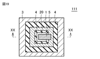
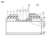
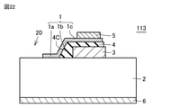
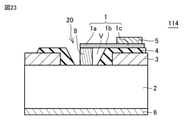
- FIG. 3 is a cross-sectional view taken along the line segment XX-XX in FIG. It is sectional drawing which shows the modification of the electromagnetic wave detector which concerns on Embodiment 13. It is sectional drawing which shows the electromagnetic wave detector which concerns on Embodiment 14. It is sectional drawing which shows the electromagnetic wave detector which concerns on Embodiment 15. FIG. It is sectional drawing which shows the modification of the electromagnetic wave detector which concerns on Embodiment 15. FIG. It is sectional drawing which shows the electromagnetic wave detector which concerns on Embodiment 16.
- the wavelength band to be detected by the electromagnetic wave detector according to the present embodiment is not particularly limited.
- the electromagnetic wave detector according to the present embodiment is a detector that detects electromagnetic waves such as visible light, infrared light, near-infrared light, ultraviolet light, X-rays, terahertz (THz) waves, and microwaves. .. In the embodiment of the present invention, these light and radio waves are collectively referred to as electromagnetic waves. Further, an arbitrary wavelength within the wavelength band to be detected by the electromagnetic wave detector according to the present embodiment is referred to as a detection wavelength.
- the electromagnetic wave detector according to the present embodiment may be provided to detect only electromagnetic waves in one wavelength band, or may be provided to detect electromagnetic waves in a plurality of wavelength bands different from each other. May be good.
- the detection wavelength of the electromagnetic wave detector according to the present embodiment may be only one or may be plural.
- the terms p-type graphene or n-type graphene are used as graphene as an example of the two-dimensional material layer, but those having more holes than the graphene in the intrinsic state are p-type and electrons. Those with many are called n-type.
- n-type or p-type terms are used for the material of the contact layer provided on graphene, which is an example of the two-dimensional material layer. These terms are, for example, n-type. If it is, a material having an electron-donating property is shown, and if it is p-type, a material having an electron-withdrawing property is shown. Further, the charge is biased in the whole molecule, and the one in which electrons are dominant is called n-type, and the one in which holes are dominant is called p-type.
- the material of these contact layers either one of organic substances and inorganic substances or a mixture thereof can be used.
- plasmon resonance phenomena such as surface plasmon resonance, which is the interaction between the metal surface and light, and pseudo-surface plasmon resonance in the sense of resonance on the metal surface outside the visible and near-infrared regions.
- these resonances are referred to as surface plasmon resonance, plasmon resonance, or simply resonance.
- Surface plasmon resonance is generally expressed as a phenomenon in which electromagnetic waves propagate or localize at the interface between a metal and a dielectric.
- surface plasmon resonance occurs not only in metal materials but also in titanium oxide and graphene, for example.
- a material in which surface plasmon resonance occurs surface plasmon is resonantly excited
- the material constituting at least a part of the surface of the plasmon filter includes a plasmon resonance material.
- the layer in which the tunnel current is not generated is called an insulating layer, and the layer in which the tunnel current can be generated is called a buffer layer.
- the material constituting the two-dimensional material layer may be any material in which atoms can be arranged in a single layer in a two-dimensional plane, such as graphene and transition metal dichalcogenide (TMD:). It may contain at least one selected from the group consisting of Transition Metal Dichalcogenide), Black Phosphorus, Silicene (two-dimensional honeycomb structure with silicon atoms), and Germanene (two-dimensional honeycomb structure with germanium atoms). ..
- transition metal dicalcogenide include molybdenum disulfide (MoS 2 ), tungsten disulfide (WS 2 ), tungsten diselened (WSe 2 ) and the like.
- a two-dimensional material layer made of at least one of the above materials has basically the same effect as a two-dimensional material layer made of graphene, which will be described later.
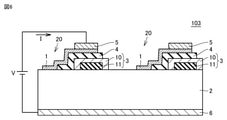
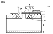
- the electromagnetic wave detector 100 includes a plurality of photoelectric conversion elements and a plasmon filter 3.
- Each photoelectric conversion element mainly includes a two-dimensional material layer 1, a semiconductor layer 2, an insulating layer 4, a first electrode portion 5, and a second electrode portion 6.
- Each photoelectric conversion element may constitute one pixel.
- the two-dimensional material layer 1 and the first electrode portion 5 of each photoelectric conversion element are provided as separate bodies from those of the other photoelectric conversion elements.
- the semiconductor layer 2 and the second electrode portion 6 of each photoelectric conversion element are provided integrally with these of the other photoelectric conversion elements.
- the insulating layer 4 of each photoelectric conversion element is provided as a separate body from, for example, the insulating layer 4 of another photoelectric conversion element.
- the insulating layer 4 of each photoelectric conversion element may be provided integrally with the insulating layer 4 of another photoelectric conversion element, for example.
- the plasmon filter 3 is arranged so as to face each of the plurality of photoelectric conversion elements.
- the plasmon filter 3 has a third surface 3A facing the first surface 2A of the semiconductor layer 2 described later, and a fourth surface 3B located on the side opposite to the third surface 3A.
- the third surface 3A is in contact with, for example, the first surface 2A of the semiconductor layer 2.
- the fourth surface 3B is in contact with the insulating layer 4.
- the plasmon filter 3 is provided so that only electromagnetic waves within the wavelength band to be detected by the electromagnetic wave detector 100 are transmitted from the fourth surface 3B side to the third surface 3A side (semiconductor layer 2 side).
- the plasmon filter 3 is provided so that surface plasmon resonance occurs when an electromagnetic wave having a detection wavelength is incident.
- the wavelength band in which the surface plasmon is excited in the plasmon filter 3 and the wavelength band in which the semiconductor layer 2 has sensitivity have a common wavelength range. Generally, it is assumed that the wavelength band in which the surface plasmon is excited is narrower than the wavelength band in which the semiconductor layer 2 has sensitivity. However, as will be described later, this may not be the case when the wavelength band in which the surface plasmon is excited is widened.
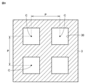
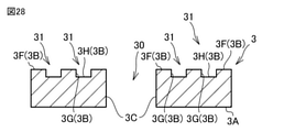
- the plasmon filter 3 is formed with a plurality of through holes 30 penetrating from the third surface 3A to the fourth surface 3B.
- the number of through holes 30 is, for example, 3 or more.
- the plurality of through holes 30 are periodically arranged in two directions, for example, along the third surface 3A and intersecting each other.
- the periodic arrangement means that the unit consisting of two or more through holes 30 is periodically arranged.
- Each of the plurality of through holes 30 is arranged at equal intervals, for example.
- the unit consisting of 3 or more through holes 30 may be periodically arranged.
- the plurality of through holes 30 may be periodically arranged at a distance from each other in at least one direction along the third surface 3A.
- the material constituting the entire surface of the plasmon filter 3 includes, for example, the above-mentioned plasmon resonance material.
- the material constituting at least a part of the surface of the plasmon filter 3 may contain the plasmon resonance material.
- only the material constituting at least the fourth surface 3B of the plasmon filter 3 and the inner peripheral surface of each of the plurality of through holes 30 contains the plasmon resonance material.
- each of the plurality of through holes 30 thickness of the plasmon filter 3
- the distance P between the central axes C of the two adjacent through holes 30 period, see FIG. 3
- the opening width of each through hole 30 is shorter than, for example, the detection wavelength.
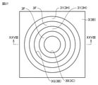
- the planar shape of the plurality of through holes 30 may be any shape as long as surface plasmon resonance occurs in the plasmon filter 3 when an electromagnetic wave having a detection wavelength is incident, but is circular as shown in FIG. 3, for example. be.
- the planar shape of the plurality of through holes 30 may be, for example, a square, a rectangle, an ellipse, a triangle, or a bullseye shape (a shape composed of one circle or ring and concentric rings arranged around the ring). It may be fractal-shaped or cross-shaped.
- surface plasmon resonance occurs when each of two or more electromagnetic waves having different detection wavelengths is applied to the plasmon filter 3.
- planar shapes of the plurality of through holes 30 may be different from each other.
- the plurality of through holes 30 may have a first through hole and a second through hole having the same planar shape as the first through hole but different in size from the first through hole. ..
- the semiconductor layer 2 has a first surface 2A and a second surface 2B located on the opposite side of the first surface 2A. As shown in FIGS. 1 and 2, the two-dimensional material layer 1, the plasmon filter 3, the insulating layer 4, and the first electrode portion 5 are arranged on the first surface 2A of the semiconductor layer 2. The second electrode portion 6 is arranged on the second surface 2B of the semiconductor layer 2.
- the electromagnetic wave detector 100 detects an electromagnetic wave incident on the semiconductor layer 2 from the side where the plasmon filter 3 is arranged.
- the semiconductor layer 2 has a plurality of regions 20 that overlap with the plurality of through holes 30 in a plan view.
- Each region 20 is a columnar region having a first surface 2A and a second surface 2B.
- the first surface 2A of the region other than the plurality of regions 20 is in contact with the third surface 3A of the plasmon filter 3.
- the first surface 2A of each region 20 is a plane with a first contact region in contact with the first portion of the two-dimensional material layer 1 described later and a second contact region in contact with a part of the insulating layer 4. It has a region exposed from the two-dimensional material layer 1, the plasmon filter 3, and the insulating layer 4 in view.
- the entire surface of the second surface 2B is in contact with the second electrode portion 6.
- the semiconductor layer 2 has sensitivity to the detection wavelength. That is, the semiconductor layer 2 is provided so that optical carriers are generated in the semiconductor layer 2 when an electromagnetic wave having a detection wavelength is incident on the semiconductor layer 2. As described above, there is a common wavelength band in the wavelength band in which the semiconductor layer 2 has sensitivity and the wavelength band in which the surface plasmon is excited in the plasmon filter 3.
- the semiconductor material constituting the semiconductor layer 2 can be arbitrarily selected according to the detection wavelength.
- the material constituting the semiconductor layer 2 may be any semiconductor material, for example, any semiconductor material of group IV, any compound semiconductor material of group III-V, or any compound semiconductor material of group II-VI. including.
- the materials constituting the semiconductor layer 2 are, for example, silicon (Si), germanium (Ge), mercury cadmium tellurium (HgCdTe), indium antimonide (InSb), lead selenium (PbSe), lead sulfur (PbS), cadmium sulfur (CdS).
- the semiconductor layer 2 may have at least one of a quantum well and a quantum dot, or may have a superlattice in which such a quantum structure is periodically arranged (for example, a Type II superlattice). ..
- the semiconductor layer 2 may have a pn junction.
- the semiconductor layer 2 is configured as an aggregate of a plurality of semiconductor layers having sensitivities to different detection wavelengths.
- the semiconductor layer 2 is doped with impurities so that the electrical resistivity of the semiconductor layer 2 is 100 ⁇ ⁇ cm or less.
- the moving speed (reading speed) of the carrier in the semiconductor layer 2 becomes high. As a result, the response speed of the electromagnetic wave detector is improved.
- the insulating layer 4 is formed so as to cover a part of the first surface 2A of the region 20 (the second contact region).
- the insulating layer 4 extends from the second contact region to a part of the fourth surface 3B of the plasmon filter 3.
- the insulating layer 4 has a portion 4a arranged on the second contact region and a portion 4b arranged on the plasmon filter 3.
- the portion 4a of the insulating layer 4 is in contact with the second contact region, a part of the inner peripheral surface of the through hole 30 of the plasmon filter 3, and the second portion 1b of the two-dimensional material layer 1 described later.
- the portion 4b of the insulating layer 4 is in contact with the third portion 1c of the two-dimensional material layer 1 described later and a part of the fourth surface 3B of the plasmon filter 3.
- the portion 4b is connected to the upper end portion of the portion 4a.
- the insulating layer 4 is formed in steps.
- the insulating layer 4 electrically insulates the semiconductor layer 2 from the second portion and the first electrode portion 5 of the two-dimensional material layer 1 described later.
- the thickness of the insulating layer 4 is not particularly limited as long as no tunnel current is generated between the second portion of the two-dimensional material layer 1 and the first electrode portion 5 and the semiconductor layer 2 during the operation of the electromagnetic wave detector 100.
- the thickness of the insulating layer 4 is as thin as possible from the viewpoint of enhancing the optical gate effect described later.
- the insulating layer 4 for example, an insulating film made of silicon oxide can be used.
- the material constituting the insulating layer 4 may be any insulating material having an electrical insulating property, and is not limited to the above-mentioned silicon oxide.
- the material constituting the insulating layer 4 is at least one selected from the group consisting of silicon oxide, tetraethyl orthosilicate, silicon nitride, hafnium oxide, aluminum oxide, nickel oxide, boron nitride, and a siloxane-based polymer material. May include.
- boron nitride has an atomic arrangement similar to that of graphene, contact with the two-dimensional material layer 1 made of graphene does not adversely affect the mobility of electric charge. Therefore, boron nitride is suitable as a material constituting the insulating layer 4 from the viewpoint of suppressing the insulating layer 4 from impairing the performance of the two-dimensional material layer 1 such as electron mobility.
- the two-dimensional material layer 1 extends from the first contact region of the region 20 to the insulating layer 4 arranged on the plasmon filter 3.
- the two-dimensional material layer 1 is arranged on the first portion 1a arranged on the other part (the first contact region) of the first surface 2A of the region 20 and on the portion 4a of the insulating layer 4. It has a second portion 1b and a plasmon filter 3 and a third portion 1c arranged on the portion 4b of the insulating layer 4.
- the first portion 1a of the two-dimensional material layer 1 is arranged on the region 20 without interposing the insulating layer 4.
- the first portion 1a is electrically connected to, for example, the first contact region of the semiconductor layer 2.
- the first portion 1a is Schottky bonded to the semiconductor layer 2.
- the second portion 1b is provided so that the electric field effect is given by the optical carriers generated in the semiconductor layer 2.
- the first portion 1a and the third portion 1c act as a source / drain region in the optical gate effect described later.
- the second portion 1b acts as a channel region in the optical gate effect described later.
- the two-dimensional material layer 1 is formed in steps.
- the number of steps of the two-dimensional material layer 1 is, for example, one more than the number of steps of the insulating layer 4, and two.
- the first portion 1a of the two-dimensional material layer 1 has one end in the longitudinal direction of the two-dimensional material layer 1.
- the third portion 1c of the two-dimensional material layer 1 has the other end in the longitudinal direction of the two-dimensional material layer 1.
- a single layer of graphene for example, a single layer of graphene can be used.
- Single-layer graphene is a monatomic layer of two-dimensional carbon crystals.
- single-layer graphene has carbon atoms in each chain arranged in a hexagonal shape.
- the two-dimensional material layer 1 may be configured as a multilayer graphene in which two or more layers of single-layer graphene are laminated.
- non-doped graphene or graphene doped with p-type or n-type impurities may be used as the two-dimensional material layer 1.
- the multi-layer graphene used as the two-dimensional material layer 1 may or may not have the same orientation of the lattice vectors of the hexagonal lattice in any two-layer graphene. For example, by laminating two or more layers of graphene, a band gap is formed in the two-dimensional material layer 1. As a result, it is possible to have a wavelength selection effect of the electromagnetic wave to be photoelectrically converted. As the number of layers in the multilayer graphene constituting the two-dimensional material layer 1 increases, the mobility of carriers in the channel region decreases.
- the two-dimensional material layer 1 is less susceptible to carrier scattering from the underlying structure such as the substrate, and as a result, the noise level is lowered. Therefore, the electromagnetic wave detector using the multilayer graphene as the two-dimensional material layer 1 can increase the light absorption and increase the detection sensitivity of the electromagnetic wave.
- the two-dimensional material layer 1 when the two-dimensional material layer 1 is in contact with the first electrode portion 5, carriers are doped from the first electrode portion 5 to the two-dimensional material layer 1.
- gold Au
- holes are generated in the two-dimensional material layer 1 in the vicinity of the first electrode portion 5 due to the difference in work functions between the two-dimensional material layer 1 and Au. Doped.
- the electromagnetic wave detector is driven in the electron conduction state in this state, the movement of electrons flowing in the channel region of the two-dimensional material layer 1 due to the influence of the holes doped in the two-dimensional material layer 1 from the first electrode portion 5 The degree decreases, and the contact resistance between the two-dimensional material layer 1 and the first electrode portion 5 increases.
- the mobility of electrons (carriers) due to the field effect in the electromagnetic wave detector decreases, and the performance of the electromagnetic wave detector may deteriorate.
- the doping amount of the carrier injected from the first electrode portion 5 is large. Therefore, the decrease in electron mobility in the electromagnetic wave detector is particularly remarkable when single-layer graphene is used as the two-dimensional material layer 1. Therefore, when the two-dimensional material layer 1 is entirely formed of single-layer graphene, the performance of the electromagnetic wave detector may deteriorate.
- the first portion 1a of the two-dimensional material layer 1 in which the carriers from the first electrode portion 5 are easily doped may be composed of multilayer graphene.
- the carrier doping from the first electrode portion 5 of the multilayer graphene is smaller than that of the single-layer graphene. Therefore, it is possible to suppress an increase in contact resistance between the two-dimensional material layer 1 and the first electrode portion 5. As a result, it is possible to suppress the above-mentioned decrease in electron mobility in the electromagnetic wave detector, and it is possible to improve the performance of the electromagnetic wave detector.
- the second portion 1b of the two-dimensional material layer 1 may be composed of single-layer graphene.
- the first portion 1a and the third portion 1c that can act as the source / drain region are composed of multilayer graphene
- the second portion 1b that can act as the channel region is a single layer. It may be composed of graphene.
- the mobility is higher than when the entire two-dimensional material layer 1 is composed of single-layer graphene
- the channel region is higher than when the entire two-dimensional material layer 1 is composed of multilayer graphene. Since the mobility of the electromagnetic detector 100 is increased, the performance of the electromagnetic wave detector 100 is improved.
- a nanoribbon-shaped graphene (hereinafter, also referred to as graphene nanoribbon) can be used.
- the two-dimensional material layer 1 for example, either a single graphene nanoribbon, a composite in which a plurality of graphene nanoribbons are laminated, or a structure in which graphene nanoribbons are periodically arranged on a plane can be used. ..
- a structure in which graphene nanoribbons are periodically arranged is used as the two-dimensional material layer 1, plasmon resonance can be generated in the graphene nanoribbons.
- the sensitivity of the electromagnetic wave detector can be improved.
- the structure in which graphene nanoribbons are periodically arranged is sometimes called a graphene metamaterial. Therefore, the above-mentioned effect can be obtained even in the electromagnetic wave detector using the graphene metamaterial as the two-dimensional material layer 1.
- the first electrode portion 5 is arranged on the above-mentioned portion 4b of the insulating layer 4, and is electrically connected to the third portion 1c of the two-dimensional material layer 1.
- the first electrode portion 5 is arranged, for example, on the third portion 1c of the two-dimensional material layer 1.
- the first electrode portion 5 is arranged so as to overlap the plasmon filter 3, the portion 4b of the insulating layer 4, and the third portion 1c of the two-dimensional material layer 1.
- the first electrode portion 5 is not arranged so as to overlap the region 20, for example.
- the second electrode portion 6 is arranged on the second surface 2B of the semiconductor layer 2.
- any material can be used as long as it is a conductor.
- the materials constituting the first electrode portion 5 and the second electrode portion 6 are, for example, gold (Au), silver (Ag), copper (Cu), aluminum (Al), nickel (Ni), chromium (Cr), and palladium. Includes at least one selected from the group consisting of (Pd).
- an adhesion layer (not shown) may be formed between the second electrode portion 6 and the semiconductor layer 2.
- the adhesion layer enhances the adhesion between the second electrode portion 6 and the semiconductor layer 2.
- the material constituting the adhesion layer contains, for example, at least one of chromium (Cr) and titanium (Ti).
- the relative positional relationship between the third portion 1c and the first electrode portion 5 of the two-dimensional material layer 1 is particularly limited as long as they are electrically connected to each other on the above-mentioned portion 4b of the insulating layer 4.
- the first electrode portion 5 may be arranged, for example, on the insulating layer 4 and below the third portion 1c of the two-dimensional material layer 1. In this case, a close contact layer may be formed between the first electrode portion 5 and the insulating layer 4.
- the adhesion layer enhances the adhesion between the first electrode portion 5 and the insulating layer 4.
- the material constituting the adhesion layer contains, for example, at least one of Cr and Ti.
- a protective film (not shown) may be formed on the two-dimensional material layer 1.
- the protective film may be provided so as to cover the periphery of the two-dimensional material layer 1, the semiconductor layer 2, and the first electrode portion 5.
- Any material can be used as the material constituting the protective film, and for example, an insulating film made of silicon oxide can be used as the protective film.
- an insulator such as an oxide or a nitride, for example, silicon oxide, silicon nitride, hafnium oxide, aluminum oxide, boron nitride or the like may be used.
- the protective film may be formed so as to embed the through hole 30. In this case, the plasmon resonance wavelength changes due to the effect of the refractive index of the protective film, but the wavelength selectivity does not change.
- each through hole 30 can be regarded as one detection unit, and in that case, the number of photoelectric conversion elements is equal to the number of through holes 30. Therefore, the electromagnetic wave detector 100 can form an image sensor by appropriately reading a signal from each photoelectric conversion element.
- the signal reading method may be, for example, a method generally used in a conventional image sensor.
- the distance between the centers of two adjacent through holes 30 does not have to be constant.
- the wavelength (resonance wavelength) of the electromagnetic wave that can be transmitted by the plasmon filter 3 is plural or widened.
- the plurality of through holes 30 have a first through hole group adjacent to each other with a first interval, and a second through hole group adjacent to each other with a second interval different from the first interval. You may.
- the semiconductor layer 2 is prepared.
- the semiconductor layer 2 is prepared as a flat substrate made of, for example, silicon.
- the second electrode portion 6 is formed on the second surface 2B of the semiconductor layer 2.
- a protective film is formed on the first surface 2A of the semiconductor layer 2.
- a resist is used as the protective film.
- the second electrode portion 6 is formed on the second surface 2B of the semiconductor layer 2.
- the adhesion layer may be formed on the back surface of the semiconductor layer 2 before the second electrode portion 6 as described above. This step may be carried out after each step described later as long as the structure on the first surface 2A of the semiconductor layer 2 can be protected. After this step, the protective film formed on the first surface 2A is removed.
- the plasmon filter 3 is formed on the first surface 2A of the semiconductor layer 2.
- the plasmon resonance material is formed on the first surface 2A.
- the film forming method is not particularly limited, and is, for example, a sputtering method or a vapor deposition method.
- a resist mask is formed on a film made of a plasmon resonance material by using photoengraving or EB drawing. The resist mask is formed so as to expose only the region where the plurality of through holes 30 should be formed in the film and cover the other regions.
- the film is partially removed by wet etching or dry etching using a resist mask as a mask. As a result, a part of the film remains under the resist mask.
- a part of this film becomes a plasmon filter 3.
- the resist mask is removed.
- the plasmon filter 3 is formed.
- the semiconductor layer 2 is formed with a plurality of regions 20 that overlap with the plurality of through holes 30 in a plan view.
- a resist mask is formed on the first surface 2A of the semiconductor layer 2 by using photoengraving or EB drawing.
- this resist mask only the region other than the plurality of regions 20 (in other words, the region in which the plasmon filter 3 should be formed) of the semiconductor layer 2 is exposed, and the plurality of regions 20 (in other words, the plurality of through holes) are exposed. 30 is formed so as to cover the region to be formed).
- the plasmon resonance material is formed on the resist mask.
- the film forming method of the film is also not particularly limited, and is, for example, a sputtering method or a vapor deposition method.
- the film is formed so as to extend from the inside of the opening of the resist mask to the upper surface of the resist mask.
- the other part of the film arranged in the opening of the resist mask remains on the plurality of regions 20 of the semiconductor layer 2 and becomes the plasmon filter 3. Become.
- the method described above is generally called a lift-off method.
- the insulating layer 4 is formed on the first surface 2A of the semiconductor layer 2 and the fourth surface 3B of the plasmon filter 3.
- an insulating film to be the insulating layer 4 is formed on the first surface 2A of the semiconductor layer 2 and the fourth surface 3B of the plasmon filter 3.
- the film forming method is not particularly limited.
- the material constituting the semiconductor layer 2 is silicon and the material constituting the insulating layer 4 is silicon oxide (SiO2)
- SiO2 silicon oxide
- the film forming method may be a CVD (Chemical Vapor Deposition) method or a sputtering method.
- a resist mask is formed on the insulating film to be the insulating layer 4 by using photoengraving or EB drawing.
- the resist mask is formed so as to cover only the region where the insulating layer 4 should be formed and expose the other regions of the insulating film.
- the insulating film is partially removed by wet etching or dry etching using a resist mask as a mask. As a result, a part of the insulating film remains under the resist mask. A part of this insulating film becomes the insulating layer 4.
- the resist mask is removed. In this way, the insulating layer 4 is formed.
- the insulating layer 4 has a portion 4a arranged on the second contact region of the region 20 and a portion 4b arranged on the fourth surface 3B of the plasmon filter 3.
- the two-dimensional material layer 1 is formed on the first contact region of each region 20 and the insulating layer 4. Specifically, first, a two-dimensional material film that should be the two-dimensional material layer 1 is formed on the first surface 2A.
- the film forming method is not particularly limited, but is, for example, an epitaxial growth method. Further, the two-dimensional material film previously formed by the CVD method or the like may be transferred and attached on the first surface 2A.
- the material constituting the two-dimensional material layer 1 contains graphene
- graphene peeled from highly oriented pyrolytic graphite (HOPG) by a mechanical peeling method may be transferred onto the first surface 2A and attached. ..
- HOPG highly oriented pyrolytic graphite
- a resist mask is formed on the two-dimensional material film by using photoengraving or EB drawing.
- the resist mask is formed so as to cover only the region where the two-dimensional material layer 1 should be formed in the two-dimensional material film.
- the two-dimensional material film is partially removed using the resist mask as a mask.
- a part of the two-dimensional material film remains under the resist mask.
- a part of this two-dimensional material film becomes the two-dimensional material layer 1.
- the resist mask is removed. In this way, the two-dimensional material layer 1 is formed.
- the two-dimensional material layer 1 has the first portion 1a, the second portion 1b, and the third portion 1c.
- the first electrode portion 5 is formed.
- the first electrode portion 5 is formed by the lift-off method described above.
- a resist mask is formed on the first surface 2A by using photoengraving or EB drawing.
- the resist mask has an opening formed in the region where the first electrode portion 5 should be formed.
- a film such as metal to be the first electrode portion 5 is formed on the resist mask.
- a thin-film deposition method, a sputtering method, or the like can be used to form the film.
- the film is formed so as to extend from the inside of the opening of the resist mask to the upper surface of the resist mask.
- the other part of the film arranged in the opening of the resist mask remains on the third portion 1c of the two-dimensional material layer 1, and the first It becomes the electrode portion 5.
- a film such as a metal film to be the first electrode portion 5 is first formed on the first surface 2A. Then, a resist mask is formed on the film by a photolithography method. The resist mask is formed so as to cover the region where the first electrode portion 5 should be formed, but is not formed in a region other than the region where the first electrode portion 5 should be formed. Then, the film is partially removed by wet etching or dry etching using a resist mask as a mask. As a result, a part of the film remains under the resist mask. A part of this film becomes the first electrode portion 5. After that, the resist mask is removed. In this way, the first electrode portion 5 may be formed.
- a protective film that protects the first portion 1a and the second portion 1b of the two-dimensional material layer 1 is formed before the film formation of the film to be the first electrode portion 5 is performed.
- the electromagnetic wave detector 100 shown in FIGS. 1 and 2 can be obtained.
- ⁇ Operating principle of electromagnetic wave detector> Next, the operating principle of the electromagnetic wave detector according to the present embodiment will be described.
- a power supply circuit for applying a voltage V is electrically connected between the first electrode portion 5 and the second electrode portion 6, and the first electrode portion 5 and the two-dimensional material layer 1 are connected.
- the semiconductor layer 2 and the second electrode portion 6 are electrically connected in the order described.
- a voltage V is applied between the first electrode portion 5 and the second electrode portion 6.
- the voltage V is set to have a reverse bias with respect to the Schottky junction between the two-dimensional material layer 1 and the semiconductor layer 2.
- An ammeter (not shown) is installed in the power supply circuit, and the ammeter monitors the current I flowing through the two-dimensional material layer 1.
- the electromagnetic wave detector 100 when the electromagnetic wave detector 100 is irradiated with an electromagnetic wave having a detection wavelength from the plasmon filter 3 side, surface plasmon resonance occurs in the plasmon filter 3.
- the transmittance is enhanced by enhancing the electromagnetic field at the resonance wavelength. The transmittance can reach almost 100%.
- the electromagnetic field is several times to several times the number when the incident electromagnetic field is 1. It is enhanced more than 10 times.
- the optical carrier receives the voltage V and is injected into the first portion 1a of the two-dimensional material layer 1 to cause a change in the current I.
- the current component that causes a change in the current I due to electromagnetic wave irradiation is called a photocurrent.
- the optical carriers generated in the semiconductor layer 2 give an electric field effect to the second portion 1b of the two-dimensional material layer 1 via the portion 4a of the insulating layer 4. As a result, the resistance value of the second portion 1b of the two-dimensional material layer 1 changes, and the current I flowing through the two-dimensional material layer 1 changes. This effect is called the optical gate effect.
- the photocurrent is amplified by the photogate effect, so that the current I changes relatively significantly.
- the electromagnetic wave detector 100 can detect the electromagnetic wave having the detection wavelength.
- the electromagnetic wave detector according to the present embodiment is not limited to the configuration for detecting the change in the current in the two-dimensional material layer 1 as described above, and is, for example, the first electrode portion 5 and the second electrode portion 5.
- a constant current may be passed between the electrode portion 6 and the change in the voltage V between the first electrode portion 5 and the second electrode portion 6 (that is, the change in the voltage value in the two-dimensional material layer 1) may be detected.
- the electromagnetic wave may be detected by using two or more of the same electromagnetic wave detectors. For example, prepare two or more of the same electromagnetic wave detectors. One electromagnetic wave detector is placed in a shielded space that is not irradiated with electromagnetic waves. Another electromagnetic wave detector is placed in the space where the electromagnetic wave to be measured is irradiated. Then, the difference between the current I or voltage V of the other electromagnetic wave detector irradiated with the electromagnetic wave and the current I or voltage V of the electromagnetic wave detector arranged in the shielded space is detected. In this way, the electromagnetic wave may be detected.
- the electromagnetic wave detector 100 includes a plurality of photoelectric conversion elements and a plasmon filter 3. A plurality of through holes 30 are periodically formed in the plasmon filter 3.
- Each photoelectric conversion element mainly includes a semiconductor layer 2, an insulating layer 4, a two-dimensional material layer 1, a first electrode portion 5, and a second electrode portion 6.
- the semiconductor layer 2 has a region 20 that overlaps with one through hole 30 in a plan view.
- the insulating layer 4 is formed so as to cover a part of the region 20.
- the two-dimensional material layer 1 is arranged on the other part of the region 20 and the insulating layer 4, and is electrically connected to the other part of the region 20.
- the first electrode portion 5 is electrically connected to the two-dimensional material layer 1.
- the second electrode portion 6 is electrically connected to the semiconductor layer 2.
- the electromagnetic wave detector 100 only the electromagnetic wave transmitted through the plasmon filter 3 is incident on the semiconductor layer 2 of the plurality of photoelectric conversion elements.
- the plasmon filter 3 has the effect of transmitting only electromagnetic waves having a specific wavelength and further improving the quantum efficiency of the semiconductor layer 2 at that wavelength. Therefore, the electromagnetic wave detector 100 can selectively detect only electromagnetic waves in a specific wavelength band with higher accuracy than the detector described in Patent Document 1 described above.
- the photoelectric conversion element is arranged on the other part of the region 20 overlapping the plurality of through holes of the plasmon filter 3 and the insulating layer 4, and is electrically connected to the other part of the region 20. Includes a two-dimensional material layer 1 that is connected in a linear manner. Therefore, as described above, in the electromagnetic wave detector 100, the photocurrent is amplified by the optical gate effect. Since the optical gate effect does not directly enhance the quantum efficiency of the photoelectric conversion material, but increases the current change due to the electromagnetic wave incident, the quantum efficiency calculated from the differential current due to the electromagnetic wave incident is equivalently over 100%. Can be done.
- the amount of change in the current I when the electromagnetic wave is incident on the electromagnetic wave detector 100 is the change in the current when the electromagnetic wave is incident on the detector described in Patent Document 1 described above in which the optical gate effect is not exhibited. Greater than quantity. Therefore, the electromagnetic wave detector 100 has higher sensitivity than the detector described in Patent Document 1 described above.
- the thickness of the two-dimensional material layer 1 is as thin as one atomic layer.
- the carrier mobility of single-layer graphene is higher than that of conventional semiconductor materials. Therefore, in the two-dimensional material layer 1, a large current change is generated with respect to a slight potential change as compared with the conventional semiconductor material. For example, the potential applied to the two-dimensional material layer 1 changes due to the change in the electric field of the semiconductor layer 2, but the amount of current change due to this potential change becomes larger than the amount of current change in a normal semiconductor.
- the current change amount in the two-dimensional material layer 1 is several hundred times to several thousand times the current change amount in a normal semiconductor. It will be about double.
- Such an electromagnetic wave detector 100 has higher sensitivity than an electromagnetic wave detector that detects only optical carriers generated in the semiconductor layer 2.
- the two-dimensional material layer 1 is electrically connected to the other part of the semiconductor layer 2 at the opening, and specifically, is Schottky-bonded to the semiconductor layer 2. Since the two-dimensional material layer 1 and the semiconductor layer 2 are Schottky-bonded, no current flows when the reverse bias is applied, and the electromagnetic wave detector 100 can be turned off.
- the electromagnetic wave detector 100 one end in the longitudinal direction of the two-dimensional material layer 1 is arranged in the region 20 of the semiconductor layer 2. Therefore, the contact state between the two-dimensional material layer 1 and the semiconductor layer 2 becomes relatively good, and the movement of optical carriers generated by electromagnetic wave irradiation is less likely to be hindered at the contact interface between the two-dimensional material layer 1 and the semiconductor layer 2. As a result, the performance of the electromagnetic wave detector 100 is improved. Further, when the optical gate effect is dominant as the effect of amplifying the photoelectric flow rate, the sensitivity of the electromagnetic wave detector 100 does not greatly depend on the contact area between the two-dimensional material layer 1 and the semiconductor layer 2.
- the area of the pixel can be reduced and the pixel can be miniaturized.
- the sensitivity of a general quantum infrared sensor inevitably decreases when the pixel area is reduced. Therefore, it is difficult to reduce the dark current.
- the electromagnetic wave detector 101 according to the second embodiment has basically the same configuration as the electromagnetic wave detector 100 according to the first embodiment, and the same effect can be obtained. It differs from the electromagnetic wave detector 100 in that the plasmon filter 3 is arranged on the side opposite to the insulating layer 4, the two-dimensional material layer 1, and the first electrode portion 5 with respect to the semiconductor layer 2.
- the insulating layer 4, the two-dimensional material layer 1, and the first electrode portion 5 are arranged on the first surface 2A of the semiconductor layer 2.
- the plasmon filter 3 and the second electrode portion 6 are arranged on the second surface 2B of the semiconductor layer 2.
- the plasmon filter 3 is arranged on the second electrode portion 6.
- the plasmon filter 3 is arranged on the side opposite to the semiconductor layer 2 with respect to the second electrode portion 6.
- the material constituting the second electrode portion 6 is a conductive material that transmits an electromagnetic wave having a detection wavelength.
- the first surface 2A of a region other than the plurality of regions 20 is in contact with the insulating layer 4.
- the first surface 2A of each region 20 is a plane with a first contact region in contact with the first portion of the two-dimensional material layer 1 described later and a second contact region in contact with a part of the insulating layer 4. It has a two-dimensional material layer 1 and a region exposed from the insulating layer 4 in view.
- the entire surface of the second surface 2B is in contact with the second electrode portion 6.
- the third surface 3A of the plasmon filter 3 is in contact with the second electrode portion 6.
- the insulating layer 4 is arranged on the first surface 2A of the semiconductor layer 2 without interposing other members. A portion of the insulating layer 4 arranged on a region other than the plurality of regions 20 is in contact with the first surface 2A of the semiconductor layer 2.
- the insulating layer 4 does not include a portion arranged on the plasmon filter 3 and is not formed in a step shape.
- the two-dimensional material layer 1 is arranged on the second contact region and the insulating layer 4 of the region 20. The portion of the two-dimensional material layer 1 arranged on the region other than the plurality of regions 20 is arranged on the insulating layer 4 in contact with the first surface 2A of the semiconductor layer 2.
- the two-dimensional material layer 1 includes a first portion 1a arranged on the first contact region and a second portion 1b arranged on the insulating layer 4, and is formed in a stepped manner. It does not include the third portion arranged on the plasmon filter 3. The number of steps of the two-dimensional material layer 1 is 1.
- the first electrode portion 5 is electrically connected to the second portion 1b of the two-dimensional material layer 1.
- the manufacturing method of the electromagnetic wave detector 101 has basically the same configuration as the manufacturing method of the electromagnetic wave detector 100, but the step of forming the plasmon filter 3 is after the step of forming the second electrode portion 6. It differs from the manufacturing method of the electromagnetic wave detector 100 in that it is carried out before the step of removing the protective film that protected the surface 2A.
- the number of steps of the two-dimensional material layer 1 is smaller than that in the electromagnetic wave detector 100, so that the manufacturing yield and the detection performance can be improved.
- the insulating layer 4 may be composed of a thermal oxide film of Si.
- the thermal oxide film has less surface irregularities and less residual charge than the electromagnetic wave detector 100 provided with the insulating layer 4 formed by the CVD method or the like. Since the mobility of the dimensional material layer 1 is not hindered, the mobility is improved and the performance of the electromagnetic wave detector 101 is improved.
- the second electrode portion 6 has the same as the insulating layer 4, the two-dimensional material layer 1, and the first electrode portion 5. It is arranged on the first surface 2A of the semiconductor layer 2.
- the plasmon filter 3 is arranged on the side opposite to the insulating layer 4, the two-dimensional material layer 1, the first electrode portion 5, and the second electrode portion 6 with respect to the semiconductor layer 2.
- the second electrode portion 6 is in contact with the first surface 2A of the semiconductor layer 2.
- the second electrode portion 6 is in contact with each first surface 2A of, for example, a region other than the plurality of regions 20 and a part of the plurality of regions 20.
- the electromagnetic wave detector 102 Since the electromagnetic wave detector 102 has basically the same configuration as the electromagnetic wave detector 101, it can exhibit the same effect as the electromagnetic wave detector 101.
- the electromagnetic wave detector 103 according to the third embodiment has basically the same configuration as the electromagnetic wave detector 100 according to the first embodiment, and the same effect can be obtained. It differs from the electromagnetic wave detector 100 in that the material constituting a part of the surface of the plasmon filter 3 contains the above-mentioned plasmon resonance material.
- the electromagnetic wave detector 103 is an electromagnetic wave detector 100 in that the plasmon filter 3 includes a first member 10 made of a plasmon resonance material and a second member 11 not made of a plasmon resonance material. Is different.
- the second member 11 is configured as, for example, a core material.
- the second member 11 has a surface in contact with the first surface 2A of the semiconductor layer 2 and another surface.
- the first member 10 is configured as a packaging material that covers the entire other surface of the second member 11.
- the material constituting the second member 11 includes, for example, a dielectric material.
- the material constituting the second member 11 contains, for example, at least one of silicon oxide and silicon nitride.
- the manufacturing method of the electromagnetic wave detector 103 has basically the same configuration as the manufacturing method of the electromagnetic wave detector 100, but in the step of forming the plasmon filter 3, the second member 11 is first formed and processed, and then the second member 11 is formed. It differs from the manufacturing method of the electromagnetic wave detector 100 in that one member 10 is formed into a film.
- the step of forming the plasmon filter 3 can be carried out only by the step of forming the film of the second member 11, the step of processing the second member 11, and the step of forming the film of the first member 10.
- the step of processing the plasmon resonance material may be unnecessary.
- the processing of dielectric materials is easier than the processing of plasmon resonance materials.
- the cost of the dielectric material is lower than the cost of Au, Ag and the like.
- the manufacturing cost of the electromagnetic wave detector 103 is lower than the manufacturing cost of the electromagnetic wave detector 100.
- the electromagnetic wave detector 103 may have the same configuration as the electromagnetic wave detector 101 or the electromagnetic wave detector 102, except that the electromagnetic wave detector 103 includes the second member 11 which is not composed of the plasmon resonance material.
- the plasmon filter 3 is the first member in which the plasmon filter 3 is made of a plasmon resonance material, similarly to the electromagnetic wave detector 103 according to the third embodiment. It differs from the electromagnetic wave detector 100 in that it includes 10 and a second member 11 which is not composed of a plasmon resonance material.
- the electromagnetic wave detector 104 has basically the same configuration as the electromagnetic wave detector 103 and can obtain the same effect, but the first member 10 and the second member 11 have a plurality of through holes 30 in each hole axial direction. It differs from the electromagnetic wave detector 103 in that it is laminated along the electromagnetic wave detector 103.
- the plasmon filter 3 is configured as a laminated body of two or more first members 10 and one or more second members 11.
- the plasmon filter 3 is composed of, for example, three or more first members 10 and two or more second members 11.
- the material constituting the first member 10 is the above-mentioned plasmon resonance material.
- the material constituting the second member 11 is a dielectric material.
- the material constituting the second member 11 contains, for example, at least one of silicon oxide and silicon nitride.
- the first member 10 and the second member 11 form a capacitance. Since such a plasmon filter 3 can act like a split ring resonator or a hyperbolic metamaterial at a detection wavelength, the refractive index becomes a negative value or zero at the detection wavelength, and as a result, a focusing effect or a lens effect is exhibited. .. As a result, the opening area of each through hole 30 in the electromagnetic wave detector 104 can be made smaller than the opening area of each through hole 30 in the electromagnetic wave detector 100. That is, the pixels of the electromagnetic wave detector 104 can be made smaller than the pixels of the electromagnetic wave detector 100. Therefore, when comparing the electromagnetic wave detector 104 and the electromagnetic wave detector 100 having the same external dimensions, the electromagnetic wave detector 104 has more pixels and can have higher resolution than the electromagnetic wave detector 100. ..
- the electromagnetic wave detector 104 is the same as the electromagnetic wave detector 101 or the electromagnetic wave detector 102 except that the first member 10 made of the plasmon resonance material and the second member 11 not made of the plasmon resonance material are included. It may have the configuration of.
- the electromagnetic wave detector according to the fifth embodiment has basically the same configuration as the electromagnetic wave detector 100 according to the first embodiment and can obtain the same effect, but the plasmon filter 3 shown in FIG. 8 It differs from the electromagnetic wave detector 100 in that the period P of the plurality of through holes 30 is specified to be equal to the detection wavelength.
- the period P is the main parameter that determines the wavelength band selected by the plasmon filter 3.
- the opening width and depth (thickness of the plasmon filter 3) of each of the plurality of through holes 30 of the plasmon filter 3 are about 1/4 of the detection wavelength.
- the period P of the plurality of through holes 30 is less likely to cause manufacturing variation as compared with the opening width and depth of each of the plurality of through holes 30. Therefore, in the electromagnetic wave detector according to the fifth embodiment, even when the opening width and the depth of each of the plurality of through holes 30 of the plasmon filter 3 are different from those of the electromagnetic wave detector 100, the detection wavelength is different. The selection performance is not easily affected by the variation.
- planar shape of each of the plurality of through holes 30 may be any shape. As shown in FIG. 8, the planar shape of the plurality of through holes 30 may be, for example, a square shape.
- the electromagnetic wave detector according to the fifth embodiment detects electromagnetic waves according to the second to fourth embodiments, except that the period P of the plurality of through holes 30 of the plasmon filter 3 is specified to be equal to the detection wavelength. It may have the same configuration as any one of the device 101 to the electromagnetic wave detector 104.
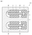
- the electromagnetic wave detector according to the sixth embodiment has basically the same configuration as the electromagnetic wave detector 100 according to the first embodiment and can obtain the same effect, but as shown in FIGS. 9 and 10. In addition, it differs from the electromagnetic wave detector 100 in that it is specified that each planar shape of the plurality of through holes 30 has a longitudinal direction and a lateral direction.
- each through hole 30 has symmetry with respect to only one virtual straight line along the third surface 3A.
- the planar shape of each through hole 30 has a longitudinal direction and a lateral direction.
- the longitudinal directions of the through holes 30 are, for example, parallel to each other.
- the lateral directions of the through holes 30 are, for example, parallel to each other.
- the electromagnetic wave detector provided with such a plasmon filter 3 can detect only a specific polarization among the electromagnetic waves having a detection wavelength.
- An electromagnetic wave detector capable of detecting such polarization can discriminate between an artificial object and a natural object, for example, discriminating oil floating on the sea surface, discriminating a vehicle in a desert, or discriminating between a human body and a road in summer. Further, an electromagnetic wave detector capable of detecting such polarization can also be used for discriminating the polarization characteristics of molecules.
- the period P in the longitudinal direction of each through hole 30 may be equal to, for example, the period P in the lateral direction of each through hole 30. Further, the period P in the longitudinal direction of each through hole 30 may be different from the period P in the lateral direction of each through hole 30, for example. Further, the arrangement of the plurality of through holes 30 may be asymmetrical in the lateral direction of each through hole 30.
- the electromagnetic wave detector according to the sixth embodiment has the second to fifth embodiments, except that it is specified that the planar shapes of the plurality of through holes 30 have the longitudinal direction and the lateral direction. It may have the same configuration as any one of the electromagnetic wave detector 101 to the electromagnetic wave detector 104 according to the above.
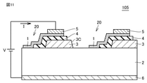
- the electromagnetic wave detector 105 according to the sixth embodiment has basically the same configuration as the electromagnetic wave detector 100 according to the first embodiment, and the same effect can be obtained. It differs from the electromagnetic wave detector 100 in that each inner peripheral surface 3C of the plurality of through holes 30 is inclined with respect to each hole axis of each through hole 30.
- the cross-sectional shape of the plasmon filter 3 is, for example, a so-called forward taper shape.
- Each inner peripheral surface 3C of the plurality of through holes 30 has an acute angle with respect to the third surface 3A and an obtuse angle with respect to the fourth surface 3B.
- the wavelength band of the resonance wavelength, the half width at half maximum, and the Q value (Quality Factor) are controlled according to the angle formed by the inner peripheral surface 3C with respect to the third surface 3A (hereinafter referred to as an inclination angle).
- the electromagnetic wave detector 105 shown in FIG. 11 has higher wavelength selectivity (monochromaticity) of the electromagnetic wave than the electromagnetic wave detector 100 shown in FIG. 1, and detects the electromagnetic wave of the detection wavelength with higher accuracy. can.
- the cross-sectional shape of the plasmon filter 3 may be, for example, a so-called reverse taper shape.
- Each inner peripheral surface 3C of the plurality of through holes 30 may have an obtuse angle with respect to the third surface 3A and an acute angle with respect to the fourth surface 3B. Basically, the larger the inclination angle, the wider the wavelength band of the electromagnetic wave transmitted by the plasmon filter 3.
- the degree of contribution of the inclination angle to the wavelength band varies depending on whether the periodicity of the plurality of through holes 30 is one-dimensional or two-dimensional, and the planar shape of the plurality of through holes 30. ..
- the electromagnetic wave detector according to the seventh embodiment relates to the second to sixth embodiments, except that it is specified that each planar shape of the plurality of through holes 30 has a longitudinal direction and a lateral direction. It may have the same configuration as any of the electromagnetic wave detector 101 to the electromagnetic wave detector 104.
- Embodiment 8 As shown in FIGS. 12 and 13, the electromagnetic wave detector 106 according to the eighth embodiment has basically the same configuration as the electromagnetic wave detector 100 according to the first embodiment, and has the same effect. It differs from the electromagnetic wave detector 100 in that the longitudinal end of the two-dimensional material layer 1 is arranged on the insulating layer 4.
- the longitudinal end of the two-dimensional material layer 1 is arranged on, for example, the insulating layer 4 arranged on the plasmon filter 3.
- the two-dimensional material layer 1 has a first portion 1a and two or more second portions 1b and a third portion 1c arranged so as to sandwich the first portion 1a.
- the longitudinal end of the two-dimensional material layer 1 may be arranged on, for example, the insulating layer 4 arranged on the region 20.
- the two-dimensional material layer 1 has a first portion 1a and a third portion 1c, and two or more second portions 1b arranged so as to sandwich the first portion 1a.
- the electromagnetic wave detector according to the eighth embodiment has the electromagnetic wave detector 101 to the electromagnetic wave according to the second to seventh embodiments, except that the longitudinal end of the two-dimensional material layer 1 is arranged on the insulating layer 4. It may have the same configuration as any of the detector 105.
- the electromagnetic wave detector 107 according to the ninth embodiment has basically the same configuration as the electromagnetic wave detector 100 according to the first embodiment and has the same effect, but has a through hole 30. It differs from the electromagnetic wave detector 100 in that the buffer layer 7 is arranged between the two-dimensional material layer 1 and the semiconductor layer 2 inside the electromagnetic wave detector 100.
- the buffer layer 7 electrically connects the first portion 1a of the two-dimensional material layer 1 and the region 20 of the semiconductor layer 2. Specifically, the buffer layer 7 is provided so that the first portion 1a of the two-dimensional material layer 1 and the first contact region of the semiconductor layer 2 are electrically connected by the tunnel current.
- the material constituting the buffer layer 7 may be any material having an electrical insulating property, and is selected from the group consisting of, for example, SiO 2 , Si 3 N 4 , HfO 2 , Al 2 O 3 , and BN. Includes at least one.
- the buffer layer 7 may be arranged on at least the first contact area in the area 20, but is arranged on, for example, the first contact area and the second contact area.
- the buffer layer 7 is provided so as to expose, for example, a part of the region 20.
- the thickness of the buffer layer 7 is set so that, for example, a tunnel current can be generated between the two-dimensional material layer 1 and the semiconductor layer 2 when an electromagnetic wave having a detection wavelength is incident.
- the thickness of the buffer layer 7 is, for example, 1 nm or more and 10 nm or less.
- the thickness of the buffer layer 7 is determined according to the detection wavelength.
- the method for producing the buffer layer 7 may be any method, and may be selected from, for example, an ALD (Atomic Layer Deposition) method, a vacuum deposition method, a sputtering method, and the like.
- the buffer layer 7 may be formed by oxidizing or nitriding the surface of the semiconductor layer 2.
- the buffer layer 7 may be a natural oxide film formed on the surface of the semiconductor layer 2.
- the buffer layer 7 suppresses the leakage current at the junction interface between the semiconductor layer 2 and the two-dimensional material layer 1, so that the dark current is higher than that of the electromagnetic wave detector 100 without the buffer layer 7. Can be reduced. Further, in the electromagnetic wave detector 107, the thickness of the buffer layer 7 is set to such a thickness that tunnel injection occurs from the semiconductor layer 2 to the two-dimensional material layer 1, so that a large light current is injected into the two-dimensional material layer 1. High sensitivity.
- the thickness of the buffer layer 7 may be thicker than the thickness capable of forming a tunnel current between the two-dimensional material layer 1 and the semiconductor layer 2, and may be thinner than the thickness of the insulating layer 4. In this case, the optical carriers generated in the semiconductor layer 2 are not injected into the two-dimensional material layer 1, and only the optical gate effect occurs. If the buffer layer 7 is thinner than the insulating layer 4, there is a carrier density gradient between the two-dimensional material layer 1 in contact with the insulating layer 4 and the two-dimensional material layer 1 in contact with the buffer layer 7. Occurs. As a result, the mobility of the two-dimensional material layer 1 is improved, so that the sensitivity is increased.
- the electromagnetic wave detector 107 according to the ninth embodiment has the second to second embodiments, except that the buffer layer 7 is arranged between the two-dimensional material layer 1 and the semiconductor layer 2 inside each through hole 30. It may have the same configuration as any one of the electromagnetic wave detector 101 to the electromagnetic wave detector 106 according to 8.
- the electromagnetic wave detector 108 according to the tenth embodiment has basically the same configuration as the electromagnetic wave detector 100 according to the first embodiment, and has the same effect, but each through hole. It differs from the electromagnetic wave detector 100 in that the connecting conductor 8 is arranged between the two-dimensional material layer 1 and the semiconductor layer 2 inside the 30.
- the connecting conductor 8 electrically connects the first portion 1a of the two-dimensional material layer 1 and the region 20 of the semiconductor layer 2.
- the first portion 1a of the two-dimensional material layer 1 is electrically connected to the first contact region of the semiconductor layer 2 via the connecting conductor 8.
- the connecting conductor 8 is ohmic-bonded to the semiconductor layer 2. Further, it is desirable that the connecting conductor 8 exhibits a high transmittance at the wavelength of the electromagnetic wave detected by the electromagnetic wave detector.
- the connecting conductor 8 may be arranged on at least the first contact region of the region 20, but is arranged on, for example, the first contact region and the second contact region.
- the connecting conductor 8 is provided so as to expose, for example, a part of the region 20.
- the connecting conductor 8 is provided between the two-dimensional material layer 1 and the semiconductor layer 2, so that the two-dimensional material layer 1 and the semiconductor layer 2 are separated from each other as compared with the electromagnetic wave detector 100.
- the contact resistance can be reduced, and the photocurrent attenuation, which is a problem when the junction between the two-dimensional material layer 1 and the semiconductor layer 2 is a Schottky junction, can be suppressed.
- the thickness of the connecting conductor 8 and the thickness of the insulating layer 4 are substantially the same, that is, the position of the upper surface of the connecting conductor 8 is substantially the same as the position of the upper surface of the insulating layer 4. It is preferable that they are the same.
- the two-dimensional material layer 1 is formed horizontally without bending, the mobility of carriers in the two-dimensional material layer 1 is improved. Since the optical gate effect is proportional to the mobility, the detection sensitivity of the electromagnetic wave detector is improved.
- the electromagnetic wave detector 108 according to the tenth embodiment is the electromagnetic wave detector 101 to the electromagnetic wave detector 106 according to the second to eighth embodiments, except that the connecting conductor 8 is formed inside each through hole 30. It may have the same configuration as any of them.
- the electromagnetic wave detector 109 according to the eleventh embodiment has basically the same configuration as the electromagnetic wave detector 100 according to the first embodiment and has the same effect, but the semiconductor layer 2 Is joined to the first semiconductor portion 21 having the first conductive type and the first semiconductor portion 21, including the second semiconductor portion 22 having the second conductive type, and the first semiconductor portion 21 and the second semiconductor portion 22. It differs from the electromagnetic wave detector 100 in that the junction interface is arranged in each region 20.
- the first semiconductor portion 21 and the second semiconductor portion 22 are arranged side by side along the first surface 2A.
- the first semiconductor portion 21 is doped with a carrier opposite to that of the second semiconductor portion 22. That is, the first semiconductor portion 21 and the second semiconductor portion 22 are pn-junctioned. At least a part of each of the first semiconductor portion 21, the second semiconductor portion 22, and the pn junction interface 23 between the first semiconductor portion 21 and the second semiconductor portion 22 is arranged in the region 20.
- the materials constituting the first semiconductor portion 21 and the second semiconductor portion 22 are, for example, the same semiconductor material.
- the pn junction interface 23 between the first semiconductor portion 21 and the second semiconductor portion 22 is arranged so as to be in contact with the first portion 1a of the two-dimensional material layer 1. Therefore, the optical carriers generated at the pn junction interface 23 between the first semiconductor portion 21 and the second semiconductor portion 22 when irradiated with electromagnetic waves can be easily taken out to the two-dimensional material layer 1. Further, the conductivity of the two-dimensional material layer 1 on the pn junction interface 23 changes under the influence of the local electric field change in the pn junction generated by the optical carrier. As a result, the detection sensitivity of the electromagnetic wave detector is improved.
- the materials constituting the first semiconductor portion 21 and the second semiconductor portion 22 may be different semiconductor materials.
- the electromagnetic wave detector 109 further includes a plasmon filter 3 provided so that a plurality of resonance wavelengths exist, the electromagnetic wave detector 109 can detect a plurality of electromagnetic waves in a narrow wavelength band.
- the electromagnetic wave detector 109 according to the eleventh embodiment is the electromagnetic wave detector 101 to the electromagnetic wave detector 108 according to the second to ninth embodiments, except that the connecting conductor 8 is formed inside each through hole 30. It may have the same configuration as any of them.
- the electromagnetic wave detector 110 according to the twelfth embodiment has basically the same configuration as the electromagnetic wave detector 100 according to the first embodiment, and has the same effect. It differs from the electromagnetic wave detector 100 in that one two-dimensional material layer 1 is electrically connected to the first contact region of each of the plurality of regions 20. In FIG. 18, the electrical wiring connected to the first electrode portion 5 and the second electrode portion 6 is omitted.
- One two-dimensional material layer 1 is electrically connected to, for example, each of two adjacent regions 20. It should be noted that one two-dimensional material layer 1 may be electrically connected to each of three or more adjacent regions 20.
- the insulating layer 4 shown in FIG. 18 only the portion located on one side of the through hole 30 is provided in a step shape, but the insulating layer 4 is located on one side of the through hole 30. Both the portion and the portion located on the other side may be provided in a step shape. From a different point of view, in the two-dimensional material layer 1 shown in FIG. 18, the number of steps of the portion located on one side of the through hole 30 is larger than the number of steps of the portion located on the other side. The number of steps of the portion of the two-dimensional material layer 1 located on one side and the portion located on the other side of the through hole 30 may be equal.
- the electromagnetic wave detector 110 since the number of regions 20 in which one two-dimensional material layer 1 is electrically connected is larger than that in the electromagnetic wave detector 100, one two-dimensional material layer 1 receives from the semiconductor layer 2. The amount of optical carriers increases. As a result, the sensitivity of the electromagnetic wave detector 110 is higher than that of the electromagnetic wave detector 100.
- the electromagnetic wave detector 110 has embodiments 2 to 10 except that one two-dimensional material layer 1 is electrically connected to the first contact region of each of the plurality of regions 20. It may have the same configuration as any one of the electromagnetic wave detector 101 to the electromagnetic wave detector 109 according to the above.
- the electromagnetic wave detector 111 according to the thirteenth embodiment has basically the same configuration as the electromagnetic wave detector 100 according to the first embodiment, and has the same effect.
- the configuration of the first electrode portion 5 and the insulating layer 4 is different from that of the electromagnetic wave detector 100.
- the insulating layer 4 and the first electrode portion 5 are formed in an annular shape, and the first portion of the two-dimensional material layer 1 is arranged inside the insulating layer 4 and the first electrode portion 5. There is.
- the electromagnetic wave detector 111 Compared with the electromagnetic wave detector 100, the electromagnetic wave detector 111 has a higher detection sensitivity because the photocurrent taken out from the semiconductor layer 2 via the two-dimensional material layer 1 increases.
- the third portion 1c of the two-dimensional material layer 1 is arranged on the first electrode portion 5, but the third portion 1c of the two-dimensional material layer 1 is from the first electrode portion 5. May be placed below.
- the two-dimensional material layer 1 is located on one side of the first electrode portion 5 with respect to the through hole 30. 1 It is electrically connected to a part of the electrode portion 5, and is also electrically connected to the other part of the first electrode portion 5 located on the other side of the through hole 30.
- the electromagnetic wave detector 112 Since the electromagnetic wave detector 112 has basically the same configuration as the electromagnetic wave detector 111, it can exhibit the same effect as the electromagnetic wave detector 111.
- the planar shape of the first electrode portion 5 may be C-shaped.
- the ends of the first electrode portion 5 may be arranged at intervals in the circumferential direction of the through hole 30. Further, in a plan view, the ends of the first electrode portion 5 may be arranged at intervals in the radial direction of the through hole 30.
- the electromagnetic wave detectors 111 and 112 according to the thirteenth embodiment have the electromagnetic wave detectors 101 to the electromagnetic wave detectors according to the second to twelve embodiments except that the insulating layer 4 and the first electrode portion 5 are formed in an annular shape. It may have the same configuration as any of 110.
- the electromagnetic wave detector 113 according to the fourteenth embodiment has basically the same configuration as the electromagnetic wave detector 100 according to the first embodiment, and the same effect can be obtained. It differs from the electromagnetic wave detector 100 in that the thickness of the insulating layer 4 changes as it approaches the first electrode portion 5 from the region 20.
- the thickness of the insulating layer 4 becomes thicker as it approaches the first electrode portion 5 from the region 20.
- the insulating layer 4 has an inclined surface 4C that is inclined with respect to the first surface 2A of the semiconductor layer 2.
- the inclination angle formed by the inclined surface 4C with respect to the first surface 2A is an acute angle. At least a part of the inclined surface 4C is arranged on the region 20.
- the two-dimensional material layer 1 extends on the inclined surface 4C. Specifically, the second portion 1b of the two-dimensional material layer 1 is arranged on the inclined surface 4C.
- the insulating layer 4 having the inclined surface 4C can be formed by any method.
- the insulating layer 4 having the inclined surface 4C may be formed by inclining the semiconductor layer 2 to form an insulating film.
- the insulating layer 4 having the inclined surface 4C may be formed by dry etching the insulating layer 4 previously formed on the semiconductor layer 2 in a state where the semiconductor layer 2 is tilted.
- the degree of electric field change in the two-dimensional material layer 1 is locally changed. Occurs. That is, when the semiconductor layer 2 is irradiated with electromagnetic waves and the electric field change is applied to the two-dimensional material layer 1, the degree of the electric field change locally changes according to the change in the thickness of the insulating layer 4. As a result, the mobility of the carriers in the two-dimensional material layer 1 is improved, and the detection sensitivity of the electromagnetic wave detector is improved.
- the electromagnetic wave detector 113 according to the fourteenth embodiment is the electromagnetic wave detector 101 according to the second to thirteenth embodiments, except that the thickness of the insulating layer 4 changes as the thickness of the insulating layer 4 approaches the first electrode portion 5.
- -It may have the same configuration as any of the electromagnetic wave detector 112.
- the electromagnetic wave detector 114 according to the fifteenth embodiment has basically the same configuration as the electromagnetic wave detector 100 according to the first embodiment, and the same effect can be obtained. It differs from the electromagnetic wave detector 100 in that a gap V is formed between the semiconductor layer 2 and the two-dimensional material layer 1.
- the first portion 1a of the two-dimensional material layer 1 that acts as a source region in the optical gate effect is electrically connected to the first contact region of the semiconductor layer 2 via the connecting conductor 8.
- the thickness of the connecting conductor 8 is preferably equal to the sum of the thickness of the plasmon filter 3 and the thickness of the insulating layer 4.
- the two-dimensional material layer 1 extends in a plane from the connecting conductor 8 to the insulating layer 4.
- the first contact region of the semiconductor layer 2 is not in contact with the two-dimensional material layer 1 but is in contact with the connecting conductor 8.
- the second portion 1b of the two-dimensional material layer 1 that acts as a source region in the optical gate effect has a portion facing the void V and a portion in contact with the insulating layer 4.
- the optical carriers generated in the semiconductor layer 2 when the electromagnetic wave is incident exert an electric field effect on the second portion 1b of the two-dimensional material layer 1 via the portion 4a of the insulating layer 4 or the void V. That is, the optical gate effect also occurs in this configuration. Since the two-dimensional material layer 1 and the semiconductor layer 2 are not in direct contact with each other, the mobility of the two-dimensional material layer 1 does not decrease. Therefore, the performance as an electromagnetic wave detector is also improved.
- the semiconductor layer 2 has a convex portion 24.
- the convex portion 24 is arranged inside the through hole 30 of the plasmon filter 3, that is, on the region 20.
- the two-dimensional material layer 1 is in contact with the convex portion 24.
- the convex portion 24 has the first contact region in contact with the first portion of the two-dimensional material layer 1 in the semiconductor layer 2.
- the height of the convex portion 24 is preferably equal to the sum of the thickness of the plasmon filter 3 and the thickness of the insulating layer 4.
- the convex portion 24 can be formed by processing the semiconductor layer 2 by photolithography, dry etching, or the like in the step of preparing the semiconductor layer 2 of the above-mentioned manufacturing method.
- the plasmon filter 3 may be formed on the semiconductor layer 2 on which the convex portion 24 is formed.
- the optical gate effect occurs. Further, since the two-dimensional material layer 1 and the insulating layer 4 are not in direct contact with each other in the void V portion, the mobility of the two-dimensional material layer 1 does not decrease. Therefore, the performance as an electromagnetic wave detector is also improved.
- the electromagnetic wave detectors 114 and 115 according to the fifteenth embodiment are the electromagnetic wave detectors 101 according to the second to fourteenth embodiments, except that a gap V is formed between the semiconductor layer 2 and the two-dimensional material layer 1. -It may have the same configuration as any of the electromagnetic wave detector 113.
- the electromagnetic wave detector 116 according to the 16th embodiment has basically the same configuration as the electromagnetic wave detector 100 according to the 1st embodiment, and the same effect can be obtained. It differs from the electromagnetic wave detector 100 in that it further includes at least one contact layer 9 in contact with the two-dimensional material layer 1.
- the contact layer 9 is arranged on, for example, the two-dimensional material layer 1.
- the contact layer 9 is made of a material capable of supplying holes or electrons to the two-dimensional material layer 1 by coming into contact with the two-dimensional material layer 1.
- the contact layer 9 allows the two-dimensional material layer 1 to be optionally doped with holes or electrons.
- a composition called a positive photoresist which contains a photosensitive agent having a quinonediagit group and a novolak resin
- a material having a polar group can be used as the material constituting the contact layer 9, for example.
- a material having an electron-withdrawing group which is an example of the material, has an effect of reducing the electron density of the two-dimensional material layer 1.
- a material having an electron donating group which is an example of the material, has an effect of increasing the electron density of the two-dimensional material layer 1.
- Examples of the material having an electron-withdrawing group include a material having a halogen, a nitrile, a carboxyl group, a carbonyl group, and the like.
- Examples of the material having an electron donating group include a material having an alkyl group, an alcohol, an amino group, a hydroxyl group and the like.
- a material in which the charge is biased in the entire molecule due to the polar group can also be used as the material for the contact layer 9.
- the material can be used as a material for the contact layer 9.
- the contact layer 9 made of an inorganic substance and the two-dimensional material layer 1 are brought into contact with each other, the conductive type to which the two-dimensional material layer 1 is doped has a work function of the contact layer 9 rather than a work function of the two-dimensional material layer 1.
- the function is large, it is p-type, and when it is small, it is n-type.
- the contact layer 9 is an organic substance
- the organic substance which is a material constituting the contact layer 9 does not have a clear work function. Therefore, whether the two-dimensional material layer 1 is an n-type dope or a p-type dope can be determined by determining the polar group of the material of the contact layer 9 based on the polarity of the organic molecule used for the contact layer 9. preferable.
- the contact layer 9 when a composition containing a photosensitive agent having a quinonediagit group and a novolak resin, which is called a positive photoresist, is used as the contact layer 9, the region where the resist is formed by the photolithography step in the two-dimensional material layer 1 is p. It becomes a mold two-dimensional material layer area. This eliminates the need for a mask forming process that comes into contact with the surface of the two-dimensional material layer 1. As a result, it is possible to reduce the process damage to the two-dimensional material layer 1 and simplify the process.
- a composition containing a photosensitive agent having a quinonediagit group and a novolak resin which is called a positive photoresist
- the electromagnetic wave detector 116 further includes a contact layer 9 in contact with the two-dimensional material layer 1.
- a contact layer 9 in contact with the two-dimensional material layer 1.
- the state (conductive type) of the two-dimensional material layer 1 is intentionally n. It can be a type or a p-type.
- the carrier doping of the two-dimensional material layer 1 can be controlled without considering the influence of the carrier doping from the first electrode portion 5 and the semiconductor layer 2. As a result, the performance of the electromagnetic wave detector can be improved.
- the contact layer 9 only on either the first electrode portion 5 side or the semiconductor layer 2 side on the upper surface of the two-dimensional material layer 1, a gradient of charge density can be created in the two-dimensional material layer 1. It is formed. As a result, the mobility of the carriers in the two-dimensional material layer 1 is improved, and the sensitivity of the electromagnetic wave detector can be increased.
- a plurality of contact layers 9 may be formed on the two-dimensional material layer 1.
- the number of contact layers 9 may be 3 or more, and may be any number.
- a plurality of contact layers 9 may be formed on the two-dimensional material layer 1 located between the first electrode portion 5 and the semiconductor layer 2. In that case, the materials of the plurality of contact layers 9 may be the same material or different materials.
- the film thickness of the contact layer 9 is preferably sufficiently thin so that photoelectric conversion can be performed when the electromagnetic wave is applied to the two-dimensional material layer 1.
- the contact layer 9 may have any configuration as long as carriers such as molecules or electrons are introduced into the two-dimensional material layer 1. For example, by immersing the two-dimensional material layer 1 in a solution and supplying carriers to the two-dimensional material layer 1 at the molecular level, the solid contact layer 9 is not formed on the two-dimensional material layer 1, but the two-dimensional material. Layer 1 may be doped with carriers.
- a material that causes polarity conversion may be used in addition to the material described above.
- the contact layer 9 undergoes polarity conversion, the electrons or holes generated during the conversion are supplied to the two-dimensional material layer 1. Therefore, electron or hole doping occurs in the portion of the two-dimensional material layer 1 in which the contact layer 9 is in contact. Therefore, even if the contact layer 9 is removed, the portion of the two-dimensional material layer 1 that has been in contact with the contact layer 9 remains doped with electrons or holes. Therefore, when a material that causes polarity conversion is used as the contact layer 9, the contact layer 9 may be removed from the two-dimensional material layer 1 after a certain period of time has elapsed.
- the polarity conversion is a phenomenon in which a polar group is chemically converted, for example, an electron attracting group is changed to an electron donating group, an electron donating group is changed to an electron attracting group, or a polar group.
- the contact layer 9 may be formed of a material that undergoes polarity conversion by electromagnetic wave irradiation.
- the contact layer 9 by selecting a material that causes a polarity conversion at a specific electromagnetic wave wavelength as the material of the contact layer 9, the contact layer 9 causes a polarity conversion only when the contact layer 9 is irradiated with an electromagnetic wave having a specific electromagnetic wave wavelength, and the two-dimensional material layer. Doping to 1 can be performed. As a result, the photocurrent flowing into the two-dimensional material layer 1 can be increased.
- a material that causes a redox reaction by electromagnetic wave irradiation may be used as the material of the contact layer 9.
- the electrons or holes generated during the redox reaction can be doped into the two-dimensional material layer 1.
- the electromagnetic wave detector 116 according to the 16th embodiment includes the electromagnetic wave detector 116 according to the 2nd to 15th embodiments, except that the electromagnetic wave detector 116 further includes at least one contact layer 9 in contact with the two-dimensional material layer 1. It may have the same configuration as any of 101 to the electromagnetic wave detector 115.
- Embodiment 17 The electromagnetic wave detector according to the 17th embodiment has basically the same configuration as the electromagnetic wave detector according to the 1st embodiment and has the same effect, but the two-dimensional material layer 1 includes a disordered layer structure portion. Therefore, it is different from the electromagnetic wave detector 100.
- the region corresponding to the channel region in the two-dimensional material layer 1 is a disordered layer structure portion.
- the random layer structure means a region in which a plurality of graphenes are laminated, and the lattices of the laminated graphenes are laminated in an inconsistent state.
- the entire two-dimensional material layer 1 may have a disordered layer structure, or only a part of the two-dimensional material layer 1 may have a disordered layer structure.
- any method can be used as a method for producing the disordered layer structure portion.
- a single-layer graphene produced by a CVD method may be transferred a plurality of times, and a multi-layer graphene may be laminated to form a disordered layer structure portion.
- graphene may be grown on graphene by a CVD method using ethanol, methane or the like as a carbon source to form a disordered layer structure portion.
- the graphene produced by the CVD method is polycrystalline, and when the graphene is further transferred onto the graphene multiple times, or when the graphene is laminated on the underlying graphene by the CVD method, the laminated graphenes are deposited with each other. It has a disordered layer structure in which the grid is in an inconsistent state.
- Graphene with a disordered layer structure is less affected by the interaction between layers and has the same properties as single-layer graphene. Further, the mobility of the two-dimensional material layer 1 is lowered due to the influence of carrier scattering in the underlying insulating layer 4. However, graphene having a disordered layer structure is affected by carrier scattering when the graphene is in contact with the insulating layer 4, but graphene in the upper layer laminated on the graphene in a disordered layer structure is affected by carrier scattering from the underlying insulating layer 4. It becomes difficult to receive. Further, in graphene having a disordered layer structure, the influence of the interaction between the layers is small, so that the conductivity is also improved. From the above, the mobility of carriers can be improved in graphene having a disordered layer structure. As a result, the sensitivity of the electromagnetic wave detector can be improved.
- graphene having a disordered layer structure may be applied only to the portion of the two-dimensional material layer 1 existing on the insulating layer 4.
- graphene having no disordered layer structure for example, single-layer graphene may be used for the contact region with the semiconductor layer 2 and the contact region with the first electrode portion 5.
- the influence of carrier scattering of the insulating layer 4 on the two-dimensional material layer 1 can be suppressed without increasing the contact resistance between the first electrode portion 5 and the semiconductor layer 2 and the two-dimensional material layer 1.
- the electromagnetic wave detector according to the 17th embodiment has the same configuration as any of the electromagnetic wave detectors 101 to 116 according to the second to 16th embodiments, except that the two-dimensional material layer 1 includes a disordered layer structure portion. May be provided.
- Embodiment 18 The electromagnetic wave detector according to the eighteenth embodiment has basically the same configuration as the electromagnetic wave detector 100 according to the first embodiment and has the same effect, but has the semiconductor layer 2, the insulating layer 4, and the contact layer 9.
- the material constituting at least one of the above is specified as a material whose characteristics are changed by irradiation with electromagnetic waves to give a change in potential to the two-dimensional material layer 1, and is different from the electromagnetic wave detector 100.
- the material constituting each of the semiconductor layer 2, the insulating layer 4, and the contact layer 9 may be a material whose characteristics are changed by irradiation with electromagnetic waves to give a change in potential to the two-dimensional material layer 1. Further, only the material constituting any one of the semiconductor layer 2, the insulating layer 4, and the contact layer 9 may be a material whose characteristics are changed by irradiation with electromagnetic waves to give a change in potential to the two-dimensional material layer 1. Further, only two constituent materials of the semiconductor layer 2, the insulating layer 4, and the contact layer 9 may be materials whose characteristics are changed by irradiation with electromagnetic waves to give a change in potential to the two-dimensional material layer 1.
- the semiconductor layer 2 is at least selected from the group consisting of, for example, a semiconductor material, a pn junction material, a metal-semiconductor junction material, a metal-insulator-semiconductor junction material, and a perovskite material (a material whose crystal structure is a perovskite structure). It is composed of one.
- the contact layer 9 is composed of at least one selected from the group consisting of quantum dots, liquid crystal materials, fullerenes, and perovskite materials.
- the insulating layer 4 is made of, for example, at least one of a ferroelectric material and a rare earth oxide.
- a ferroelectric material having a polarization effect (pyroelectric effect) due to electromagnetic waves is used as the ferroelectric material, the polarization of the ferroelectric material is changed by irradiation with electromagnetic waves. As a result, the potential can be changed in the two-dimensional material layer 1.
- the contact layer 9 When the contact layer 9 is made of a material that gives a change in potential to the two-dimensional material layer 1 as described above, the contact layer 9 does not necessarily have to be in direct contact with the two-dimensional material layer 1.
- the contact layer 9 may be provided so as to come into contact with the upper surface or the lower surface of the two-dimensional material layer 1 via, for example, an insulating film.
- the material constituting at least one of the semiconductor layer 2, the insulating layer 4, and the contact layer 9 has characteristics changed by irradiation with electromagnetic waves, and the potential of the two-dimensional material layer 1 is changed. It may have the same configuration as any of the electromagnetic wave detectors according to the second to seventeenth embodiments, except that it is specified as a material that gives a change in the above.
- the electromagnetic wave detector according to the nineteenth embodiment has basically the same configuration as the electromagnetic wave detector 100 according to the first embodiment and has the same effect, but has the same effect as that of the inner peripheral surfaces 3C of the plurality of through holes 30. It differs from the electromagnetic wave detector 100 in that the cross-sectional shape is a step shape (step shape).
- the cross-sectional shape is a step shape (step shape).
- FIG. 26 only the peripheral structure of one through hole 30 of the plasmon filter 3 of the electromagnetic wave detector according to the nineteenth embodiment is shown, and the peripheral structure of the other through holes 30 of the plasmon filter 3 and other members are shown. Illustration is omitted.
- the inner peripheral surface 3C has a plurality of (for example, two) step surfaces 3D and a plurality of (for example, three) terrace surfaces 3E.
- Each step surface 3D extends, for example, along the hole axis of the through hole 30.
- Each terrace surface 3E intersects the hole axis of the through hole 30 and has a ring shape in a plan view.
- the centers of the terrace surfaces 3E overlap each other, for example.
- the center of each terrace surface 3E overlaps, for example, the center of the through hole 30.
- Each terrace surface 3E is orthogonal to, for example, the hole axis of the through hole 30.
- the dimensions of each step surface 3D are, for example, equal to each other.
- each terrace surface 3E is, for example, equal to each other.
- the upper end of the outermost step surface 3D (uppermost step surface 3D) in the radial direction with respect to the center of each through hole 30 is connected to the inner peripheral end portion of the fourth surface 3B.
- the insulating layer 4 and the two-dimensional material layer 1 are arranged on a plurality of step surfaces 3D, a plurality of terrace surfaces 3E, and a fourth surface 3B of the plasmon filter 3.
- At least one of the plurality of through holes 30 may have the structure shown in FIG. 26, but for example, each of the plurality of through holes 30 of the plasmon filter 3 has the structure shown in FIG. 26. Have.
- the electromagnetic wave detector according to the nineteenth embodiment as compared with the electromagnetic wave detector 100, higher-order diffraction is less likely to occur in the plasmon filter 3 when the electromagnetic wave is applied to the plasmon filter 3, so that the electromagnetic wave transmitted through the plasmon filter 3 is transmitted.
- the strength of can be enhanced.
- each step surface 3D may have a forward taper shape.
- each step surface 3D may be inclined so that the distance from the third surface 3A increases as the distance from the center of the through hole 30 increases.
- the electromagnetic wave detector according to the nineteenth embodiment is the electromagnetic wave detector according to the second to eighteenth embodiments, except that the cross-sectional shape of each inner peripheral surface 3C of the plurality of through holes 30 is a step shape (step shape). It may have the same configuration as any of them.
- the electromagnetic wave detector according to the 20th embodiment has basically the same configuration as the electromagnetic wave detector 100 according to the 1st embodiment and has the same effect, but has one penetration on the fourth surface 3B of the plasmon filter 3. It differs from the electromagnetic wave detector 100 in that a plurality of groove portions 31 (drilling) surrounding the hole 30 are formed. 27 and 28 show only the peripheral structure of one through hole 30 of the plasmon filter 3 of the electromagnetic wave detector according to the 20th embodiment, and the peripheral structure of the other through holes 30 of the plasmon filter 3 and others. The illustration of the member of is omitted.
- the centers of a plurality of (for example, two) groove portions 31 overlap each other.
- the center of each groove 31 overlaps, for example, the center of one through hole 30.
- the fourth surface 3B of the plasmon filter 3 has a so-called bullseye structure in a plan view.
- the fourth surface 3B has a plurality of (for example, three) top surfaces 3F, a plurality of (for example, four) wall surfaces 3G, and a plurality of (for example, two) bottom surfaces 3H.
- Each groove 31 has two wall surfaces 3G and one bottom surface 3H.
- the two wall surfaces 3G of each groove 31 face each other in the radial direction of the through hole 30 with respect to the hole axis.
- the upper end of each wall surface 3G is connected to the inner peripheral end or the outer peripheral end of each top surface 3F.
- the lower end of each wall surface 31A is connected to the inner peripheral end or the outer peripheral end of each bottom surface 3H.
- Each wall surface 3G extends, for example, along the hole axis of the through hole 30.
- Each top surface 3F and each bottom surface 3H are orthogonal to, for example, the hole axis of the through hole 30.
- the inner peripheral end portion of the top surface 3F located on the innermost side in the radial direction with respect to the center of the through hole 30 is connected to the upper end portion of the inner peripheral surface 3C.
- the insulating layer 4 and the two-dimensional material layer 1 are arranged on a plurality of top surfaces 3F, a plurality of wall surfaces 3G, and a plurality of bottom surfaces 3H of the plasmon filter 3.
- the first electrode portion 5 is arranged, for example, on the top surface 3F located on the outermost side in the radial direction with respect to the center of the through hole 30.
- each groove 31 surrounds only one through hole 30. In a plan view, each groove 31 does not surround two adjacent through holes 30.
- At least one of the plurality of through holes 30 may have the structure shown in FIGS. 27 and 28, for example, each of the plurality of through holes 30 is shown in FIGS. 27 and 28. It has a structure.
- the electromagnetic wave detector according to the 20th embodiment when an electromagnetic wave is incident on the fourth surface 3B on which the groove portion 31 is formed, a propagation type surface plasmon resonance occurs in the plasmon filter 3. Since the surface plasmon resonance propagates through the fourth surface 3B on which the plurality of groove portions 31 are formed and is guided to the through hole 30, the intensity of the electromagnetic wave transmitted through the plasmon filter 3 can be enhanced.
- the detection wavelength is determined by the shape of the plurality of groove portions 31 (period of the plurality of groove portions 31, dimensions of each groove portion 31, etc.), the plurality of groove portions 31 are formed.
- the degree of freedom in setting the detection wavelength is higher than that of the electromagnetic wave detector 100 that has not been used.
- the plasmon filter 3 may be formed with at least one groove 31.
- the number of grooves 31 may be one. Further, the number of groove portions 31 may be 3 or more.
- the distance between the two groove portions 31 adjacent to each other in the radial direction is, for example, equal to each other. By doing so, the wavelength selectivity (monochromaticity) is enhanced.
- the intervals between the groove portions 31 adjacent to each other in the radial direction may be different from each other. By doing so, the wavelength band of the electromagnetic wave transmitted through the plasmon filter 3 becomes wide.
- each wall surface 3G may have a forward taper shape.
- each wall surface 3G may be inclined so that the distance from the third surface 3A increases as the distance from the center of the through hole 30 increases.
- the electromagnetic wave detector according to the 20th embodiment is the electromagnetic wave detector according to the 2nd to 19th embodiments, except that at least one groove 31 surrounding the through hole 30 is formed on the 4th surface 3B of the plasmon filter 3. It may have the same configuration as any of the above.
- the electromagnetic wave detector array 300 according to the 21st embodiment is an aggregate of a plurality of electromagnetic wave detectors 200.
- Each electromagnetic wave detector 200 is any one of the electromagnetic wave detectors 100 to 116 according to the first to the twentyth embodiments.
- a plurality of electromagnetic wave detectors 200 are periodically arranged two-dimensionally.
- the plurality of electromagnetic wave detectors 200 may be periodically arranged one-dimensionally. Further, the arrangement of the plurality of electromagnetic wave detectors 200 is not periodic, and may be arranged at different intervals.
- the electromagnetic wave detectors 200 are arranged in a 2 ⁇ 2 matrix.
- the number of electromagnetic wave detectors 200 to be arranged is not limited to this.
- a plurality of electromagnetic wave detectors 200 may be arranged in a matrix of 3 or more ⁇ 3 or more.
- the second electrode portion 6 can be used as a common electrode. It is also good.
- the wiring of pixels can be reduced as compared with the electromagnetic wave detector array in which the second electrode portions 6 of each electromagnetic wave detector 200 are independent of each other. , The resolution becomes higher.
- a current cutoff structure such as a semiconductor layer 2 trench structure may be formed.
- the electromagnetic wave detector array 300 can also be used as an image sensor by arranging a plurality of electromagnetic wave detectors 200 in an array.
- the detection wavelengths of the electromagnetic wave detectors 200 may be the same as each other, but may be different from each other.
- the electromagnetic wave detector array 300 may include a read circuit configured to read a signal from each electromagnetic wave detector 200.
- Each electromagnetic wave detector 200 may be arranged on the readout circuit.
- the read format of the read circuit is, for example, a CTAI (Capacitive Transimpedance Amplifier) type.
- the readout circuit may be in another readout format.
- the electromagnetic wave detector array 300 may include a bump that electrically connects the first electrode portion 5 of each electromagnetic wave detector 200 and the readout circuit.
- the structure in which each electromagnetic wave detector 200 and the readout circuit are connected by bumps is called a hybrid junction.
- Hybrid junction is a common structure in quantum infrared sensors.
- each electromagnetic wave detector 200 further includes, for example, a pad electrically connected to the first electrode portion 5, and each bump is electrically connected to the pad.
- the material of the bump is, for example, a conductive material such as indium (Ib).
- the material of the pad is a conductive material such as an aluminum silicon (Al—Si) alloy, nickel (Ni), or gold (Au).
- the electromagnetic wave detector array 301 shown in FIG. 30 has basically the same configuration as the electromagnetic wave detector array 300 and has the same effect, but has different types of electromagnetic wave detectors 200, 201, as a plurality of electromagnetic wave detectors. It differs from the electromagnetic wave detector array 300 in that it includes 202 and 203. Each electromagnetic wave detector 200, 201, 202, 203 is any one of the electromagnetic wave detectors 100 to 116 according to the first to twenty-odd embodiments.
- electromagnetic wave detectors 200, 201, 202, and 203 of different types are arranged in a matrix.
- the electromagnetic wave detectors 200, 201, 202, and 203 are arranged in a 2 ⁇ 2 matrix, but the number of electromagnetic wave detectors arranged is not limited to this. Further, in the present embodiment, different types of electromagnetic wave detectors 200, 201, 202, and 203 are arranged periodically in two dimensions, but they may be arranged periodically in one dimension. Further, different types of electromagnetic wave detectors 200, 201, 202, 203 may be arranged at different intervals instead of periodically.
- the electromagnetic wave detectors 200, 201, 202, and 203 of different types according to any one of the first to the 20th embodiments are arranged in a one-dimensional or two-dimensional array to form an image sensor. It can have the function as.
- electromagnetic wave detectors 200, 201, 202, and 203 electromagnetic wave detectors having different detection wavelengths may be used.
- electromagnetic wave detectors having different detection wavelength selectivity may be prepared from the electromagnetic wave detectors according to any one of embodiments 1 to 20 and arranged in an array. In this case, the electromagnetic wave detector aggregate can detect at least two or more electromagnetic waves having different wavelengths.
- the electromagnetic wave detectors 200, 201, 202, and 203 having different detection wavelengths in an array for example, ultraviolet light, infrared light, terahertz wave, and radio wave are arranged in the same manner as the image sensor used in the visible light region.
- the wavelength of the electromagnetic wave can be identified in any wavelength range such as the wavelength range of. As a result, it is possible to obtain a colorized image showing, for example, a difference in wavelength as a difference in color.
- each semiconductor layer 2 of each electromagnetic wave detector 200, 201, 202, 203 may be made of a material having a different detection wavelength.
- a semiconductor material whose detection wavelength is the wavelength of visible light and a semiconductor material whose detection wavelength is the wavelength of infrared rays may be used as the constituent materials.
- the electromagnetic wave detector when the electromagnetic wave detector is applied to an in-vehicle sensor, the electromagnetic wave detector can be used as a camera for a visible light image in the daytime.
- the electromagnetic wave detector can also be used as an infrared camera at night. By doing so, it is not necessary to properly use a camera having an image sensor depending on the detection wavelength of the electromagnetic wave.
- the electromagnetic wave detector can be used as a position detection sensor capable of detecting the position of an object even with a small number of pixels.
- the electromagnetic wave detectors 200, 201, 202, 203 having different detection wavelengths are used as described above, an image sensor that detects the intensity of electromagnetic waves having a plurality of wavelengths can be obtained. This makes it possible to detect electromagnetic waves having a plurality of wavelengths and obtain a color image without using a color filter, which has been conventionally required for CMOS image sensors and the like.
- polarization identification image sensor by arranging electromagnetic wave detectors 200, 201, 202, 203 having different polarizations to be detected.
- polarization imaging can be performed by arranging a plurality of electromagnetic wave detectors for each unit, with four pixels having detection angles of 0 °, 90 °, 45 °, and 135 ° as one unit.
- the polarization identification image sensor enables, for example, identification of artificial and natural objects, material identification, identification of objects of the same temperature in the infrared wavelength region, identification of boundaries between objects, or equivalent improvement in resolution.
- the electromagnetic wave detector aggregate according to the present embodiment configured as described above can detect electromagnetic waves in a wide wavelength range. Further, the electromagnetic wave detector aggregate according to the present embodiment can detect electromagnetic waves having different wavelengths.
Landscapes
- Physics & Mathematics (AREA)
- Engineering & Computer Science (AREA)
- Mathematical Physics (AREA)
- Theoretical Computer Science (AREA)
- Spectroscopy & Molecular Physics (AREA)
- Health & Medical Sciences (AREA)
- Life Sciences & Earth Sciences (AREA)
- Chemical & Material Sciences (AREA)
- Analytical Chemistry (AREA)
- Biochemistry (AREA)
- General Health & Medical Sciences (AREA)
- General Physics & Mathematics (AREA)
- Immunology (AREA)
- Pathology (AREA)
- Light Receiving Elements (AREA)
Abstract
Description
図1および図2に示されるように、実施の形態1に係る電磁波検出器100は、複数の光電変換素子と、プラズモンフィルタ3とを備える。各光電変換素子は、二次元材料層1、半導体層2、絶縁層4、第1電極部5、および第2電極部6を主に備える。各光電変換素子は、1つの画素を構成し得る。各光電変換素子の二次元材料層1および第1電極部5は、他の光電変換素子のこれらと別体として設けられている。各光電変換素子の半導体層2および第2電極部6は、他の光電変換素子のこれらと一体として設けられている。各光電変換素子の絶縁層4は、例えば他の光電変換素子の絶縁層4と別体として設けられている。なお、各光電変換素子の絶縁層4は、例えば他の光電変換素子の絶縁層4と一体として設けられていてもよい。
まず、半導体層2を準備する。半導体層2は、例えばシリコン等からなる平坦な基板として準備される。
<電磁波検出器の動作原理>
次に、本実施の形態に係る電磁波検出器の動作原理について説明する。
本実施の形態に係る電磁波検出器100は、複数の光電変換素子と、プラズモンフィルタ3とを備える。プラズモンフィルタ3には、複数の貫通孔30が周期的に形成されている。各光電変換素子は、半導体層2、絶縁層4、二次元材料層1、第1電極部5、および第2電極部6を主に備える。半導体層2は、平面視において1つの貫通孔30と重なる領域20を有する。絶縁層4は、領域20の一部を覆うように形成されている。二次元材料層1は、領域20の他の一部および絶縁層4上に配置され、かつ領域20の上記他の一部と電気的に接続されている。第1電極部5は、二次元材料層1と電気的に接続されている。第2電極部6は、半導体層2と電気的に接続されている。
図4に示されるように、実施の形態2に係る電磁波検出器101は、実施の形態1に係る電磁波検出器100と基本的に同様の構成を備え、同様の効果を得ることができるが、プラズモンフィルタ3が半導体層2に対して絶縁層4、二次元材料層1、および第1電極部5とは反対側に配置されている点で、電磁波検出器100とは異なる。
図5に示されるように、電磁波検出器101の変形例である電磁波検出器102では、第2電極部6が、絶縁層4、二次元材料層1、および第1電極部5と同様に、半導体層2の第1面2A上に配置されている。プラズモンフィルタ3は、半導体層2に対して絶縁層4、二次元材料層1、第1電極部5、および第2電極部6とは反対側に配置されている。第2電極部6は、半導体層2の第1面2Aと接触している。第2電極部6は、例えば複数の領域20以外の他の領域、および複数の領域20のうちの一部の領域20の各第1面2Aと接触している。
図6に示されるように、実施の形態3に係る電磁波検出器103は、実施の形態1に係る電磁波検出器100と基本的に同様の構成を備え、同様の効果を得ることができるが、プラズモンフィルタ3の表面の一部を構成する材料が、上述したプラズモン共鳴材料を含む点で、電磁波検出器100とは異なる。言い換えると、電磁波検出器103は、プラズモンフィルタ3が、プラズモン共鳴材料により構成されている第1部材10と、プラズモン共鳴材料により構成されていない第2部材11とを含む点で、電磁波検出器100とは異なる。
図7に示されるように、実施の形態4に係る電磁波検出器104は、実施の形態3に係る電磁波検出器103と同様に、プラズモンフィルタ3が、プラズモン共鳴材料により構成されている第1部材10と、プラズモン共鳴材料により構成されていない第2部材11とを含む点で、電磁波検出器100とは異なる。
実施の形態5に係る電磁波検出器は、実施の形態1に係る電磁波検出器100と基本的に同様の構成を備え、同様の効果を得ることができるが、図8に示されるプラズモンフィルタ3の複数の貫通孔30の周期Pが検出波長と等しいことが特定されている点で、電磁波検出器100とは異なる。
実施の形態6に係る電磁波検出器は、実施の形態1に係る電磁波検出器100と基本的に同様の構成を備え、同様の効果を得ることができるが、図9および図10に示されるように、複数の貫通孔30の各平面形状が長手方向および短手方向を有していることが特定されている点で、電磁波検出器100とは異なる。
図11に示されるように、実施の形態6に係る電磁波検出器105は、実施の形態1に係る電磁波検出器100と基本的に同様の構成を備え、同様の効果を得ることができるが、複数の貫通孔30の各内周面3Cが各貫通孔30の各孔軸に対して傾斜している点で、電磁波検出器100とは異なる。
図12および図13に示されるように、実施の形態8に係る電磁波検出器106は、実施の形態1に係る電磁波検出器100と基本的に同様の構成を備え、同等の効果を奏するが、二次元材料層1の長手方向の端部が絶縁層4上に配置されている点で、電磁波検出器100とは異なる。
図14に示されるように、実施の形態9に係る電磁波検出器107は、実施の形態1に係る電磁波検出器100と基本的に同様の構成を備え、同等の効果を奏するが、貫通孔30の内部において、二次元材料層1と半導体層2との間にバッファ層7が配置されている点で、電磁波検出器100とは異なる。
図15に示されるように、実施の形態10に係る電磁波検出器108は、実施の形態1に係る電磁波検出器100と基本的に同様の構成を備え、同様の効果を奏するが、各貫通孔30の内部において、二次元材料層1と半導体層2との間に接続導電体8が配置されている点で、電磁波検出器100と異なっている。
図16に示されるように、実施の形態11に係る電磁波検出器109は、実施の形態1に係る電磁波検出器100と基本的に同様の構成を備え、同様の効果を奏するが、半導体層2が第1導電型を有する第1半導体部分21と第1半導体部分21と接合され、第2導電型を有する第2半導体部分22とを含み、第1半導体部分21と第2半導体部分22との接合界面が各領域20内に配置されている点で、電磁波検出器100と異なっている。
図17および図18に示されるように、実施の形態12に係る電磁波検出器110は、実施の形態1に係る電磁波検出器100と基本的に同様の構成を備え、同等の効果を奏するが、1つの二次元材料層1が複数の領域20の各々の上記第1接触領域と電気的に接続されている点で、電磁波検出器100とは異なる。なお、図18では、第1電極部5および第2電極部6に接続される電気配線は省略されている。
図19および図20に示されるように、実施の形態13に係る電磁波検出器111は、実施の形態1に係る電磁波検出器100と基本的に同様の構成を備え、同等の効果を奏するが、第1電極部5および絶縁層4の構成が電磁波検出器100と異なっている。
図21に示されるように、電磁波検出器111の変形例としての電磁波検出器112では、二次元材料層1が、第1電極部5のうち貫通孔30に対して一方の側に位置する第1電極部5の一部分と電気的に接続されているとともに、貫通孔30に対して他方の側に位置する第1電極部5の他の一部分と電気的に接続されている。
図22に示されるように、実施の形態14に係る電磁波検出器113は、実施の形態1に係る電磁波検出器100と基本的には同様の構成を備え、同様の効果を得ることができるが、絶縁層4の厚さが領域20から第1電極部5に近づくにつれて変化している点で、電磁波検出器100と異なる。
図23に示されるように、実施の形態15に係る電磁波検出器114は、実施の形態1に係る電磁波検出器100と基本的には同様の構成を備え、同様の効果を得ることができるが、半導体層2と二次元材料層1との間に空隙Vが形成されている点で、電磁波検出器100と異なる。
図24に示されるように、電磁波検出器114の変形例としての電磁波検出器115では、半導体層2が、凸部24を有している。凸部24は、プラズモンフィルタ3の貫通孔30の内部、すなわち領域20上に配置されている。二次元材料層1は、凸部24と接触している。凸部24は、半導体層2において二次元材料層1の第1部分と接触している上記第1接触領域を有している。凸部24の高さは、図24に示すようにプラズモンフィルタ3の厚さと絶縁層4の厚さとの和と等しいことが好ましい。なお、凸部24は、上述した製造方法の半導体層2を準備する工程において、半導体層2をフォトリソグラフィおよびドライエッチングなどで加工することによって形成され得る。プラズモンフィルタ3は、凸部24が形成された半導体層2上に形成され得る。
図25に示されるように、実施の形態16に係る電磁波検出器116は、実施の形態1に係る電磁波検出器100と基本的に同様の構成を備え、同様の効果を得ることができるが、二次元材料層1と接触している少なくとも1つ以上の接触層9をさらに備えている点で、電磁波検出器100と異なっている。
実施の形態17に係る電磁波検出器は、実施の形態1に係る電磁波検出器と基本的に同様の構成を備え、同様の効果を奏するが、二次元材料層1が乱層構造部分を含む点で、電磁波検出器100と異なる。
実施の形態18に係る電磁波検出器は、実施の形態1に係る電磁波検出器100と基本的に同様の構成を備え、同様の効果を奏するが、半導体層2、絶縁層4、および接触層9の少なくともいずれかを構成する材料が、電磁波の照射により特性が変化し二次元材料層1に電位の変化を与える材料に特定されている点で、電磁波検出器100とは異なる。
実施の形態19に係る電磁波検出器は、実施の形態1に係る電磁波検出器100と基本的に同様の構成を備え、同様の効果を奏するが、複数の貫通孔30の各内周面3Cの断面形状が階段形状(ステップ形状)である点で、電磁波検出器100とは異なる。図26では、実施の形態19に係る電磁波検出器のプラズモンフィルタ3の1つの貫通孔30の周辺構造のみが図示されており、プラズモンフィルタ3の他の貫通孔30の周辺構造および他の部材の図示が省略されている。
実施の形態20に係る電磁波検出器は、実施の形態1に係る電磁波検出器100と基本的に同様の構成を備え、同様の効果を奏するが、プラズモンフィルタ3の第4面3Bに1つの貫通孔30を囲む複数の溝部31(堀り込み)が形成されている点で、電磁波検出器100とは異なる。図27および図28は、実施の形態20に係る電磁波検出器のプラズモンフィルタ3の1つの貫通孔30の周辺構造のみが図示されており、プラズモンフィルタ3の他の貫通孔30の周辺構造および他の部材の図示が省略されている。
図29に示されるように、実施の形態21に係る電磁波検出器アレイ300は、複数の電磁波検出器200の集合体である。各電磁波検出器200は、実施の形態1~実施の形態20に係る電磁波検出器100~116のいずれかである。
図30に示される電磁波検出器アレイ301は、電磁波検出器アレイ300と基本的に同様の構成を備え、同様の効果を奏するが、複数の電磁波検出器として種類の異なる電磁波検出器200、201,202,203を備えている点で、電磁波検出器アレイ300とは異なる。各電磁波検出器200、201,202,203は、実施の形態1~実施の形態20に係る電磁波検出器100~116のいずれかである。
Claims (26)
- 少なくとも1つの光電変換素子と、
前記少なくとも1つの光電変換素子と対向するように配置されたプラズモンフィルタとを備え、
前記プラズモンフィルタには、複数の貫通孔が周期的に形成されており、
前記少なくとも1つの光電変換素子は、
平面視において前記複数の貫通孔のうちの少なくとも1つの貫通孔と重なる領域を有する半導体層と、
前記領域の一部を覆うように形成された絶縁層と、
前記領域の他の一部および前記絶縁層上に配置され、かつ前記領域の前記他の一部と電気的に接続されている二次元材料層と、
前記二次元材料層と電気的に接続された第1電極部と、
前記半導体層と電気的に接続された第2電極部とを備える、電磁波検出器。 - 前記少なくとも1つの光電変換素子において、
前記半導体層は、平面視において前記複数の貫通孔のうちの2以上の貫通孔の各々と重なる複数の領域を有し、
前記二次元材料層は、前記複数の領域の各々の前記他の一部と電気的に接続されている、請求項1に記載の電磁波検出器。 - 前記プラズモンフィルタは、前記半導体層に対して、前記絶縁層、前記二次元材料層、および前記第1電極部と同じ側に配置されており、
前記絶縁層は、前記領域の一部上から前記プラズモンフィルタの一部上にまで延在しており、
前記二次元材料層は、前記領域の前記他の一部から前記プラズモンフィルタ上に配置された前記絶縁層上にまで延在しており、
前記第1電極部は、前記プラズモンフィルタ上に配置された前記絶縁層上に配置されている、請求項1または2に記載の電磁波検出器。 - 前記プラズモンフィルタは、前記半導体層に対して、前記絶縁層、前記二次元材料層、および前記第1電極部とは反対側に配置されている、請求項1または2に記載の電磁波検出器。
- 前記プラズモンフィルタの表面の少なくとも一部を構成する材料は、電磁波が入射したときに表面プラズモン共鳴が生じる材料である、請求項1~4のいずれか1項に記載の電磁波検出器。
- 前記プラズモンフィルタは、芯材と、前記芯材の表面の少なくとも一部上に配置された包材とを含み、
前記包材を構成する材料は、電磁波が入射したときに表面プラズモン共鳴が生じる材料である、請求項5に記載の電磁波検出器。 - 前記プラズモンフィルタは、前記複数の貫通孔の各々の孔軸方向に沿って積層された第1部材と第2部材とを含み、
前記第1部材を構成する材料は、電磁波が入射したときに表面プラズモン共鳴が生じる材料であり、
前記第2部材を構成する材料は、誘電体である、請求項5に記載の電磁波検出器。 - 前記プラズモンフィルタにおいて表面プラズモンが励起される波長帯域は、前記半導体層が感度を有する波長帯域よりも狭い、請求項1~7のいずれか1項に記載の電磁波検出器。
- 前記複数の貫通孔は、少なくとも一方向に沿って周期的に配列されている、請求項1~8のいずれか1項に記載の電磁波検出器。
- 前記半導体層は、検出波長に感度を有し、
前記複数の貫通孔の周期は、前記検出波長と等しい、請求項9に記載の電磁波検出器。 - 前記複数の貫通孔の各内周面は、前記複数の貫通孔の各孔軸に対して傾斜している、請求項1~10のいずれか1項に記載の電磁波検出器。
- 前記複数の貫通孔の各内周面の断面形状は、階段形状である、請求項1~11のいずれか1項に記載の電磁波検出器。
- 平面視において、前記プラズモンフィルタの前記表面には、前記複数の貫通孔の1つの貫通孔を囲む少なくとも1つの溝部が形成されている、請求項1~12のいずれか1項に記載の電磁波検出器。
- 前記二次元材料層の端部は、前記領域上に配置されている、請求項1~13のいずれか1項に記載の電磁波検出器。
- 前記半導体層の前記領域と前記二次元材料層との間に配置されたバッファ層をさらに備える、請求項1~14のいずれか1項に記載の電磁波検出器。
- 前記バッファ層は、前記二次元材料層と前記半導体層との間にトンネル電流を形成することが可能な厚さを有する、請求項15に記載の電磁波検出器。
- 前記半導体層の前記領域と前記二次元材料層とを電気的に接続する接続導電体をさらに備える、請求項1~14のいずれか1項に記載の電磁波検出器。
- 前記半導体層は、
第1導電型を有する第1半導体部分と、
前記第1半導体部分と接合され、第2導電型を有する第2半導体部分とを含み、
前記第1半導体部分と前記第2半導体部分との接合界面は、前記領域内に配置されている、請求項1~17のいずれか1項に記載の電磁波検出器。 - 前記第1半導体部分の吸収波長は、前記第2半導体部分の吸収波長とは異なる、請求項18に記載の電磁波検出器。
- 平面視において、前記第1電極部は環状に形成されており、かつ前記領域は前記第1電極部よりも内側に配置されている、請求項1~19のいずれか1項に記載の電磁波検出器。
- 前記絶縁層の厚みは、前記領域から前記第1電極部に近づくにつれて変化する、請求項1~20のいずれか1項に記載の電磁波検出器。
- 前記半導体層と前記二次元材料層との間に空隙が形成されている、請求項1~21のいずれか1項に記載の電磁波検出器。
- 前記二次元材料層に接触するように配置された接触層をさらに備える、請求項1~22のいずれか1項に記載の電磁波検出器。
- 前記二次元材料層は、遷移金属ダイカルコゲナイド、グラフェン、黒リン、シリセン、ゲルマネン、グラフェンナノリボンおよびボロフェンからなるグループから選択されるいずれかの材料を含む、請求項1~23のいずれか1項に記載の電磁波検出器。
- 前記二次元材料層は、乱層構造部分を含み、
前記乱層構造部分は、少なくとも前記絶縁層上に配置されている、請求項1~24のいずれか1項に記載の電磁波検出器。 - 請求項1~25のいずれか1項に記載の電磁波検出器を複数備え、
前記複数の電磁波検出器が、第1方向および第2方向の少なくともいずれかに沿って並んで配置されている、電磁波検出器アレイ。
Priority Applications (3)
| Application Number | Priority Date | Filing Date | Title |
|---|---|---|---|
| US18/013,572 US12543402B2 (en) | 2020-08-25 | 2021-05-13 | Electromagnetic wave detector including a photoelectric conversion element and a plasmon filter, and electromagnetic wave detector array |
| CN202180055848.2A CN116057716A (zh) | 2020-08-25 | 2021-05-13 | 电磁波检测器以及电磁波检测器阵列 |
| JP2022545313A JP7403670B2 (ja) | 2020-08-25 | 2021-05-13 | 電磁波検出器および電磁波検出器アレイ |
Applications Claiming Priority (2)
| Application Number | Priority Date | Filing Date | Title |
|---|---|---|---|
| JP2020141687 | 2020-08-25 | ||
| JP2020-141687 | 2020-08-25 |
Publications (1)
| Publication Number | Publication Date |
|---|---|
| WO2022044447A1 true WO2022044447A1 (ja) | 2022-03-03 |
Family
ID=80353046
Family Applications (1)
| Application Number | Title | Priority Date | Filing Date |
|---|---|---|---|
| PCT/JP2021/018235 Ceased WO2022044447A1 (ja) | 2020-08-25 | 2021-05-13 | 電磁波検出器および電磁波検出器アレイ |
Country Status (4)
| Country | Link |
|---|---|
| US (1) | US12543402B2 (ja) |
| JP (1) | JP7403670B2 (ja) |
| CN (1) | CN116057716A (ja) |
| WO (1) | WO2022044447A1 (ja) |
Cited By (2)
| Publication number | Priority date | Publication date | Assignee | Title |
|---|---|---|---|---|
| WO2023210108A1 (ja) * | 2022-04-25 | 2023-11-02 | 三菱電機株式会社 | 電磁波検出器及び電磁波検出器アレイ |
| JP2024509637A (ja) * | 2021-02-01 | 2024-03-04 | アプライド マテリアルズ インコーポレイテッド | シリコン含有光学デバイス構造を有する遷移金属ジカルコゲナイドでコーティングされた平面光学デバイス |
Families Citing this family (1)
| Publication number | Priority date | Publication date | Assignee | Title |
|---|---|---|---|---|
| JP7550854B2 (ja) * | 2020-06-15 | 2024-09-13 | 三菱電機株式会社 | 電磁波検出器および電磁波検出器アレイ |
Citations (4)
| Publication number | Priority date | Publication date | Assignee | Title |
|---|---|---|---|---|
| US20180106933A1 (en) * | 2016-10-13 | 2018-04-19 | University Of Central Florida Research Foundation, Inc. | Optical detector device with patterned graphene layer and related methods |
| CN108305912A (zh) * | 2017-01-11 | 2018-07-20 | 中国科学院上海微系统与信息技术研究所 | 具有波长选择性的石墨烯仿生光探测器及其制备方法 |
| US20200056992A1 (en) * | 2017-04-25 | 2020-02-20 | The Regents Of The University Of Michigan | Plasmo photoelectronic immunosensor |
| CN111341875A (zh) * | 2020-03-11 | 2020-06-26 | 电子科技大学 | 一种石墨烯/二硒化钯/硅异质结自驱动光电探测器 |
Family Cites Families (2)
| Publication number | Priority date | Publication date | Assignee | Title |
|---|---|---|---|---|
| US20150243826A1 (en) | 2012-08-28 | 2015-08-27 | Northeastern University | Tunable heterojunction for multifunctional electronics and photovoltaics |
| KR20230162602A (ko) * | 2021-03-31 | 2023-11-28 | 소니 세미컨덕터 솔루션즈 가부시키가이샤 | 광 검출 장치 및 전자 기기 |
-
2021
- 2021-05-13 WO PCT/JP2021/018235 patent/WO2022044447A1/ja not_active Ceased
- 2021-05-13 JP JP2022545313A patent/JP7403670B2/ja active Active
- 2021-05-13 CN CN202180055848.2A patent/CN116057716A/zh active Pending
- 2021-05-13 US US18/013,572 patent/US12543402B2/en active Active
Patent Citations (4)
| Publication number | Priority date | Publication date | Assignee | Title |
|---|---|---|---|---|
| US20180106933A1 (en) * | 2016-10-13 | 2018-04-19 | University Of Central Florida Research Foundation, Inc. | Optical detector device with patterned graphene layer and related methods |
| CN108305912A (zh) * | 2017-01-11 | 2018-07-20 | 中国科学院上海微系统与信息技术研究所 | 具有波长选择性的石墨烯仿生光探测器及其制备方法 |
| US20200056992A1 (en) * | 2017-04-25 | 2020-02-20 | The Regents Of The University Of Michigan | Plasmo photoelectronic immunosensor |
| CN111341875A (zh) * | 2020-03-11 | 2020-06-26 | 电子科技大学 | 一种石墨烯/二硒化钯/硅异质结自驱动光电探测器 |
Cited By (4)
| Publication number | Priority date | Publication date | Assignee | Title |
|---|---|---|---|---|
| JP2024509637A (ja) * | 2021-02-01 | 2024-03-04 | アプライド マテリアルズ インコーポレイテッド | シリコン含有光学デバイス構造を有する遷移金属ジカルコゲナイドでコーティングされた平面光学デバイス |
| JP7686776B2 (ja) | 2021-02-01 | 2025-06-02 | アプライド マテリアルズ インコーポレイテッド | シリコン含有光学デバイス構造を有する遷移金属ジカルコゲナイドでコーティングされた平面光学デバイス |
| WO2023210108A1 (ja) * | 2022-04-25 | 2023-11-02 | 三菱電機株式会社 | 電磁波検出器及び電磁波検出器アレイ |
| JP7422963B1 (ja) * | 2022-04-25 | 2024-01-26 | 三菱電機株式会社 | 電磁波検出器 |
Also Published As
| Publication number | Publication date |
|---|---|
| US20230343882A1 (en) | 2023-10-26 |
| US12543402B2 (en) | 2026-02-03 |
| JP7403670B2 (ja) | 2023-12-22 |
| CN116057716A (zh) | 2023-05-02 |
| JPWO2022044447A1 (ja) | 2022-03-03 |
Similar Documents
| Publication | Publication Date | Title |
|---|---|---|
| JP6884288B1 (ja) | 電磁波検出器 | |
| US10784394B2 (en) | Electromagnetic wave detector and electromagnetic wave detector array | |
| US11876141B2 (en) | Electronic device using graphene, manufacturing method for the device, and electromagnetic wave detector including the device | |
| JP7550854B2 (ja) | 電磁波検出器および電磁波検出器アレイ | |
| US12295176B2 (en) | Electromagnetic wave detector and electromagnetic wave detector assembly | |
| JP7403670B2 (ja) | 電磁波検出器および電磁波検出器アレイ | |
| JP7374222B2 (ja) | 電磁波検出器および電磁波検出器集合体 | |
| JP7123282B1 (ja) | 電磁波検出器および電磁波検出器アレイ | |
| JP7422963B1 (ja) | 電磁波検出器 | |
| JP7740896B2 (ja) | 電磁波検出器および電磁波検出器集合体 | |
| US20250185515A1 (en) | Electromagnetic wave detector, electromagnetic wave detector array, and image sensor | |
| WO2023112770A1 (ja) | 電磁波検出器及び電磁波検出器アレイ | |
| JP7562054B1 (ja) | 電磁波検出器及び電磁波検出器アレイ | |
| WO2024100784A1 (ja) | 電磁波検出器および電磁波検出器集合体 |
Legal Events
| Date | Code | Title | Description |
|---|---|---|---|
| 121 | Ep: the epo has been informed by wipo that ep was designated in this application |
Ref document number: 21860879 Country of ref document: EP Kind code of ref document: A1 |
|
| ENP | Entry into the national phase |
Ref document number: 2022545313 Country of ref document: JP Kind code of ref document: A |
|
| NENP | Non-entry into the national phase |
Ref country code: DE |
|
| 122 | Ep: pct application non-entry in european phase |
Ref document number: 21860879 Country of ref document: EP Kind code of ref document: A1 |
|
| WWG | Wipo information: grant in national office |
Ref document number: 18013572 Country of ref document: US |