WO2022044228A1 - 電力変換装置 - Google Patents
電力変換装置 Download PDFInfo
- Publication number
- WO2022044228A1 WO2022044228A1 PCT/JP2020/032480 JP2020032480W WO2022044228A1 WO 2022044228 A1 WO2022044228 A1 WO 2022044228A1 JP 2020032480 W JP2020032480 W JP 2020032480W WO 2022044228 A1 WO2022044228 A1 WO 2022044228A1
- Authority
- WO
- WIPO (PCT)
- Prior art keywords
- module
- inverter module
- inverter
- power conversion
- conversion device
- Prior art date
- Legal status (The legal status is an assumption and is not a legal conclusion. Google has not performed a legal analysis and makes no representation as to the accuracy of the status listed.)
- Ceased
Links
Images


Classifications
-
- H—ELECTRICITY
- H02—GENERATION; CONVERSION OR DISTRIBUTION OF ELECTRIC POWER
- H02M—APPARATUS FOR CONVERSION BETWEEN AC AND AC, BETWEEN AC AND DC, OR BETWEEN DC AND DC, AND FOR USE WITH MAINS OR SIMILAR POWER SUPPLY SYSTEMS; CONVERSION OF DC OR AC INPUT POWER INTO SURGE OUTPUT POWER; CONTROL OR REGULATION THEREOF
- H02M7/00—Conversion of AC power input into DC power output; Conversion of DC power input into AC power output
- H02M7/42—Conversion of DC power input into AC power output without possibility of reversal
- H02M7/44—Conversion of DC power input into AC power output without possibility of reversal by static converters
- H02M7/48—Conversion of DC power input into AC power output without possibility of reversal by static converters using discharge tubes with control electrode or semiconductor devices with control electrode
Definitions
- the present invention relates to a power conversion device.
- JP2015-89244A discloses a power conversion device in which two inverter circuits for driving two different motors and a smoothing capacitor connected to an input terminal of each inverter circuit are arranged in one housing.
- the JP2015-89244A has a configuration in which a smoothing capacitor is arranged between the two inverter circuits, the size of the entire power conversion device becomes large.
- the present invention aims to reduce the size of the power conversion device.
- a first inverter circuit a first inverter module having a first input terminal and a first output terminal connected to the first inverter circuit, a second inverter circuit, and a second inverter.
- a second inverter module having a second input terminal and a second output terminal connected to a circuit, a capacitor module connected to the first inverter module and the second inverter module, a first inverter module, a second inverter module,
- a power conversion device including a housing for accommodating a capacitor module and a capacitor module.
- the first inverter module and the second inverter module are arranged adjacent to each other, and the first input terminal and the first output terminal are the edges of the first inverter module facing the second inverter module.
- the second input terminal and the second output terminal are arranged adjacent to different edges, the second input terminal and the second output terminal are arranged adjacent to the edge different from the edge facing the first inverter module of the second inverter module, and the capacitor module is the first. It is arranged so as to be stacked on the inverter module and the second inverter module, and is connected to the first input terminal and the second input terminal.
- FIG. 1 is a perspective view of the power conversion device of the first embodiment.
- FIG. 2 is a plan view (before mounting the capacitor module) of the power conversion device of the first embodiment.
- FIG. 3 is a plan view (after mounting the capacitor module) of the power conversion device of the first embodiment.
- FIG. 4 is a side view of the power conversion device of the first embodiment.
- FIG. 5 is a circuit diagram of the power conversion device of the first embodiment.
- FIG. 6 is a plan view of the power conversion device of the first comparative example.
- FIG. 7 is a plan view (before mounting the capacitor module) of the power conversion device of the modified example of the first embodiment.
- FIG. 8 is a plan view (after mounting the capacitor module) of the power conversion device of the modified example of the first embodiment.
- FIG. 1 is a perspective view of the power conversion device of the first embodiment.
- FIG. 2 is a plan view (before mounting the capacitor module) of the power conversion device of the first embodiment.
- FIG. 3 is a plan view (
- FIG. 9 is a plan view of the power conversion device of the second comparative example.
- FIG. 10 is a plan view of the power conversion device of the third comparative example.
- FIG. 11 is a plan view of the power conversion device of the fourth comparative example.
- FIG. 12 is a plan view of the power conversion device of the second embodiment.
- FIG. 13 is a plan view of the power conversion device of the third embodiment.
- FIG. 14 is a side view of the power conversion device of the fourth embodiment.
- FIG. 15 is a side view of the power conversion device of the fifth embodiment.
- FIG. 16 is a plan view of the power conversion device of the sixth embodiment.
- FIG. 17 is a perspective view of an example of a connector connected to the power conversion device of the sixth embodiment.
- FIG. 18 is a plan view of the power conversion device of the seventh embodiment.
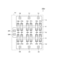
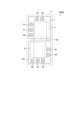
- FIG. 1 is a perspective view of the power conversion device 100 of the first embodiment.
- FIG. 2 is a plan view of the power conversion device 100 of the first embodiment (before mounting the capacitor module 3).
- FIG. 3 is a plan view of the power conversion device 100 of the first embodiment (after mounting the capacitor module 3).
- FIG. 4 is a side view of the power conversion device 100 of the first embodiment.
- the first inverter module 1, the second inverter module 2, and the capacitor module 3 are housed inside the rectangular housing 4, and the bottom surface inside the housing 4 is accommodated.
- a first inverter module 1 and a second inverter module 2 are mounted therein, and a capacitor module 3 is arranged so as to be laminated on the first inverter module 1 and the second inverter module 2.
- a lid portion 5 is arranged on the upper portion of the housing 4, and the opening of the housing 4 is closed.
- the power conversion device 100 of the first embodiment is mounted on, for example, an electric vehicle (not shown).
- An electric vehicle includes an engine (internal combustion engine), a power generation motor that generates power by the driving force of the engine, a drive motor, and a battery, and the engine or the drive motor drives the drive wheels.
- the power generation motor supplies electric power to the battery, and the drive motor receives electric power from the battery to drive the motor.
- the first inverter module 1 for example, the single-phase side is connected to the battery and the three-phase side is connected to the drive motor (hereinafter, simply referred to as a motor).
- the second inverter module 2 for example, the single-phase side is connected to the battery and the three-phase side is connected to the power generation motor (hereinafter, simply referred to as a motor).
- the first inverter module 1 is a plate-shaped component having a first inverter circuit 11 (see FIG. 5) inside and having a rectangular (square, rectangular) shape in a plan view.
- the first input terminals 1P, 1N and the first output terminals 1U, 1V, 1W are arranged on the upper surface of the first inverter module 1.
- the first input terminals 1P and 1N are connected to the single-phase side of the first inverter circuit 11 and are connected to the capacitor module 3.
- the first output terminals 1U, 1V, 1W are connected to the three-phase side of the first inverter circuit 11 and are electrically connected to the motor of the electric vehicle.
- the first input terminals 1P and 1N are arranged adjacent to the edge side of one of the four edges of the first inverter module 1. Further, the first output terminals 1U, 1V, 1W are adjacent to the edge side of one of the two edges adjacent to the edge where the first input terminals 1P, 1N are arranged adjacent to each other in the first inverter module 1. Are arranged. Therefore, in the first input terminals 1P, 1N and the first output terminals 1U, 1V, 1W, the letters "L" are inverted left and right in a plan view on the two adjacent edge sides of the first inverter module 1 (or It is arranged so as to form the design of the letter "L").
- the second inverter module 2 includes a second inverter circuit 21 corresponding to the first inverter circuit 11, and second input terminals 2P and 2N corresponding to the first input terminals 1P and 1N. Further, the second inverter module 2 includes second output terminals 2U, 2V, 2W corresponding to the first output terminals 1U, 1V, 1W, which are electrically connected to the motor of the electric vehicle.
- the first inverter module 1 has a second inverter module 2 having an edge on which the first input terminals 1P, 1N and the first output terminals 1U, 1V, 1W are not arranged. It is arranged so as to face the.
- the second inverter module 2 is arranged so that the edges on which the second input terminals 2P, 2N and the second output terminals 2U, 2V, 2W are not arranged face the first inverter module 1.
- the second inverter module 2 is arranged adjacent to the first inverter module 1 in a state of being rotated 180 degrees from the direction of the first inverter module 1.
- the first inverter module 1 and the second inverter module 2 may be mounted on the bottom surface of the housing 4 in a state of being in contact with each other.
- the first input terminals 1P and 1N of the first inverter module 1 are arranged so as to face the side wall which is one short side of the housing 4 in a plan view, and the second input terminal 2P of the second inverter module 2 is arranged. , 2N are arranged so as to face the side wall which is the other short side of the housing 4 in a plan view.
- first output terminals 1U, 1V, 1W of the first inverter module 1 face one long side of the housing 4 in a plan view and are side walls of the one long side and are on the short side side of the one.
- the second output terminals 2U, 2V, 2W of the second inverter module 2 face the side wall of the other long side of the housing 4 in a plan view and are the side walls of the other long side. It is placed on the short side of.
- the capacitor module 3 has, for example, a rectangular parallelepiped module main body 31, and the module main body 31 is a resin-sealed smoothing capacitor 32 or the like (see FIG. 5).
- the module main body 31 has a first input terminal 1N, 1P, a first output terminal 1U, 1V, 1W, a second input terminal 2P, 2N, a second output terminal 2U, 2V, in a plan view. It is arranged so that it does not overlap with 2W. That is, the module main body 31 is surrounded by the first input terminal 1N, 1P, the first output terminal 1U, 1V, 1W, the second input terminal 2P, 2N, and the second output terminal 2U, 2V, 2W in a plan view. Placed inside the area.
- the first connection terminal 34P from the short side facing the first input terminals 1P and 1N.
- 34N bus bar
- the second connection terminals 35P, 35N extend from the short side facing the second input terminals 2P, 2N, and these are connected to the second input terminals 2P, 2N.
- the first connection terminals 34P, 34N and the second connection terminals 35P, 35N have an L-shape.
- the first connection terminal 34P is arranged so that the tip extending in the horizontal direction overlaps the first input terminal 1P, and is screwed to the first input terminal 1P.
- the first connection terminal 34N is arranged so that the tip extending in the horizontal direction overlaps the first input terminal 1N, and is screwed to the first input terminal 1N.
- the second connection terminal 35P is arranged so that the tip extending in the horizontal direction overlaps the second input terminal 2P, and is screwed to the second input terminal 2P. Further, the second connection terminal 35N is arranged so that the tip extending in the horizontal direction overlaps the second input terminal 2N, and is screwed to the second input terminal 2N.
- the capacitor module 3 is arranged so that the module main body 31 is laminated on the first inverter module 1 and the second inverter module 2 in such a manner that the module main body 31 is supported by the first connection terminals 34P, 34N and the second connection terminals 35P, 35N.
- An element (not shown) for driving the first inverter circuit 11 is arranged on the upper surface of the first inverter module 1 (the same applies to the second inverter module 2), and the elements are the module main body 31 and the first inverter. It may be configured to be arranged between modules 1.
- the third connection terminals 36P and 36N extend from the long side (or the side surface of the long side) of the lower surface of the module main body 31.
- the third connection terminals 36P and 36N are electrically connected to the battery of the electric vehicle.
- the third connection terminals 36P, 36N are the first input terminals 1P, 1N (first connection terminals 34P, 34N), the first output terminals 1U, 1V, 1W, and the second input terminals 2P, 2N (second connection) in a plan view. It can be arranged at an arbitrary position that does not overlap with the terminals 35P, 35N) and the second output terminals 2U, 2V, 2W.
- the module main body 31 is a resin-sealed smoothing capacitor 32 and the like, and the first connection terminals 34P, 34N, the second connection terminals 35P, 35N, and the third connection terminals 36P, 36N are provided from the lower surface side. It is extended.
- the upper surface side of the module main body 31 is insulated. Therefore, as shown in FIG. 4, since there is no possibility of a short circuit between the upper side of the module main body 31 and the lid portion 5, both can be brought close to each other, and the dimension in the thickness direction of the power conversion device 100 can be increased accordingly. It can be made smaller.
- a heat sink is formed on the outer bottom surface of the housing 4, and the housing 4 is attached to the refrigerant passage so that the outer bottom surface of the housing 4 and the heat sink come into contact with the refrigerant. It has become. Therefore, the power conversion device 100 can dissipate heat to the refrigerant.
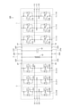
- FIG. 5 is a circuit diagram of the power conversion device 100 of the first embodiment. As shown in FIG. 5, in the power conversion device 100 of the present embodiment, the first inverter module 1 and the second inverter module 2 are connected in parallel to the capacitor module 3.
- the first inverter module 1 (first inverter circuit 11) includes a parallel circuit of a power transistor 12A such as an IGBT (InsuKated Gate BipoCar Transistor) and a feedback diode 13A, and a parallel circuit of the power transistor 12B and the feedback diode 13B.
- a power transistor 12A such as an IGBT (InsuKated Gate BipoCar Transistor)
- IGBT Insulation Gate BipoCar Transistor
- feedback diode 13A a parallel circuit of the power transistor 12B and the feedback diode 13B.
- Three series circuits (series circuit 11U, series circuit 11V, series circuit 11W) connected in series are connected in parallel.
- the positive electrode side of the series circuit 11U, 11V, 11W is connected in parallel to the first input terminal 1P, and the negative electrode side of the series circuit 11U, 11V, 11W is connected in parallel to the first input terminal 1N.
- connection midpoint UM of the series circuit 11U is connected to the first output terminal 1U
- connection midpoint VM of the series circuit 11V is connected to the first output terminal 1V
- connection midpoint WM of the series circuit 11W is the first output terminal 1W. It is connected to the.
- the series circuits 11U, 11V, 11W receive the PWM signal, they output a three-phase AC signal via the first output terminals 1U, 1V, 1W, but the motor of the electric vehicle. Generates a regenerative current, the regenerative power is input via the first output terminals 1U, 1V, 1W, and this is converted into a single layer current and output to the first input terminals 1P, 1N (battery). ..
- the second inverter module 2 (second inverter circuit 21) has a parallel circuit of the power transistor 22A and the feedback diode 23A and a parallel circuit of the power transistor 22B and the feedback diode 23B in series as in the first inverter module 1.
- Three series circuits (series circuit 21U, series circuit 21V, series circuit 21W) connected to the above are connected in parallel, and operate in the same manner as the first inverter module 1.
- the positive electrode side of the series circuit 21U, 21V, 21W is connected in parallel to the second input terminal 2P, and the negative electrode side of the series circuit 21U, 21V, 21W is connected in parallel to the second input terminal 2N.
- connection midpoint UM of the series circuit 21U is connected to the second output terminal 2U
- connection midpoint VM of the series circuit 21V is connected to the second output terminal 2V
- connection midpoint WM of the series circuit 21W is the second output terminal 2W. It is connected to the.
- the capacitor module 3 includes first connection terminals 34P, 34N, second connection terminals 35P, 35N, and third connection terminals 36P, 36N outside the module body 31, and a smoothing capacitor 32 inside the module body 31. It is provided with a resistor 33 and internal wiring 37P, 37N (bus bar).
- One end of the internal wiring 37P is connected to the first connection terminal 34P, and the other end is connected to the second connection terminal 35P. Further, the third connection terminal 36P, one end of the smoothing capacitor 32, and one end of the resistor 33 are connected to the internal wiring 37P.
- One end of the internal wiring 37N is connected to the first connection terminal 34N, and the other end is connected to the second connection terminal 35N. Further, the third connection terminal 36N, the other end of the smoothing capacitor 32, and the other end of the resistor 33 are connected to the internal wiring 37N.
- the resistor 33 discharges the electric charge stored in the smoothing capacitor 32 and consumes it as heat when the operations of the first inverter module 1 and the second inverter module 2 are stopped, but it may be omitted. ..
- the first input terminal 1P is directly connected to the first connection terminal 34P (bus bar), and the first input terminal 1N is also directly connected to the first connection terminal 34N (bus bar).
- the second input terminal 2P is directly connected to the second connection terminal 35P (bus bar), and the second input terminal 2N is also directly connected to the second connection terminal 35N (bus bar).
- FIG. 6 is a plan view of the power conversion device 100J of the first comparative example.
- the same components are assigned the same number, and the description thereof will be omitted unless necessary.
- the power conversion device 100J of the first comparative example has the same configuration as the above-mentioned JP2015-89244A. That is, the first inverter module 1J, the second inverter module 2J, and the capacitor module 3J are mounted on the bottom surface inside the housing 4J. The capacitor module 3J is arranged between the first inverter module 1J and the second inverter module 2J.
- the first inverter module 1J is provided with first output terminals 1U, 1V, 1W. Further, the first inverter module 1J has first input terminals 1PU and 1NU to which a direct current for outputting a three-phase AC current (U phase) is input from the first output terminal 1U, and three phases from the first output terminal 1V. The first input terminals 1PV, 1NV to which the DC current for outputting the AC current (V phase) is input, and the DC current for outputting the three-phase AC current (W phase) from the first output terminal 1W are input. First input terminals 1PW and 1NW are provided.
- the second inverter module 2J includes second output terminals 2U, 2V, 2W, and further includes second input terminals 2PU, 2NU, 2PV, 2NV, 2PW, 2NW.
- Third connection terminals 36P and 36N are connected to the longitudinal end of the capacitor module 3J.
- a plurality of fourth connection terminals 38P are arranged so as to face the first input terminals 1PU, 1PV, 1PW and the second input terminals 2PU, 2PV, 2PW, respectively.
- a plurality of fourth connection terminals 38N are arranged so as to face the first input terminals 1NU, 1NV, 1NW and the second input terminals 2NU, 2NV, 2NW, respectively.
- the fourth connection terminal 38P is electrically connected to the first input terminals 1PU, 1PV, 1PW and the second input terminals 2PU, 2PV, 2PW facing each other via the relay bus bar 6, and the fourth connection terminal 38N is opposed to each other. It is connected to the first input terminals 1NU, 1NV, 1NW, and the second input terminals 2NU, 2NV, 2NW via the relay bus bar 6.
- connection terminal 38P is electrically connected to the third connection terminal 36P via the internal wiring 37P (FIG. 5) arranged inside the module main body 31.
- the fourth connection terminal 38N is electrically connected to the third connection terminal 36N via an internal wiring 37N (FIG. 5) arranged inside the module main body 31.
- the capacitor module 3J is arranged between the first inverter module 1J and the second inverter module 2J as described above. Therefore, the size of the housing 4J and the power conversion device 100J in a plan view becomes large.
- the capacitor module 3 is not arranged between the first inverter module 1 and the second inverter module 2, and the first inverter module 1 and the second inverter are not arranged.
- the modules 2 are arranged adjacent to each other (or in contact with each other), and the capacitor module 3 is arranged so as to be laminated on the first inverter module 1 and the second inverter module 2.
- the arrangement position of the third connection terminals 36P and 36N is limited to the short side side of the capacitor module 3J that does not face the first inverter module 1J and the second inverter module 2J. Will be done. Therefore, when changing the position (when the power conversion device 100J is mounted on an electric vehicle whose battery side terminal is not on the short side), a separate bus bar is used to connect the third connection terminals 36P and 36N to the battery side terminal. Need to be connected, which increases cost and size.
- the capacitor module 3 is arranged on the first inverter module 1 and the second inverter module 2.
- the third connection terminals 36P, 36N are the first input terminals 1P, 1N (first connection terminals 34P, 34N), the first output terminals 1U, 1V, 1W, and the second input terminal in a plan view. It can be placed at any position that does not overlap with the 2P, 2N (second connection terminal 35P, 35N) and the second output terminal 2U, 2V, 2W, and can be connected to the terminal on the battery side without using a separate bus bar. It is possible to avoid an increase in cost and size accordingly.
- FIG. 7 is a plan view (before mounting of the capacitor module 3A) of the power conversion device 100A of the modified example of the first embodiment.
- FIG. 8 is a plan view (after mounting the capacitor module 3A) of the power conversion device 100A of the modified example of the first embodiment.
- FIG. 9 is a plan view of the power conversion device 100K of the second comparative example.
- the second inverter module 2 is 90 degrees to the left from the same direction as the first inverter module 1. It is arranged adjacent to the first inverter module 1 in a rotated state.
- the first output terminals 1U, 1V, 1W face the side wall of the long side of the housing 4, and the second output terminals 2U, 2V, 2W face the side wall of the short side of the housing 4.
- the second connection terminals 35P and 35N extend from the side surface of the long side of the module main body 31 and are arranged so as to overlap the second input terminals 2P and 2N.
- the third connection terminals 36P and 36N are arranged on the side surface of the module main body 31 facing the side surface of the long side where the second connection terminals 35P and 35N are arranged, for example.
- the internal wiring 37N, 37P (see FIG. 5) is arranged inside the module main body 31 according to the arrangement of the second connection terminals 35P, 35N and the third connection terminals 36P, 36N. ing.
- the first output terminals 1U, 1V, and 1W are arranged so as to face the side wall of the short side of the housing 4, but the first inverter module 1 is rotated 90 degrees to the right to the housing. It is also possible to arrange it so as to face the side wall of the short side of 4.
- the first connection terminals 34P and 34N are arranged on the side surface of the long side of the module main body 31 so as to overlap the first input terminals 1P and 1N in a plan view, and the internal wiring 37N and 37P (see FIG. 5) are connected to the first. 1
- the arrangement inside the module main body 31 is changed according to the arrangement of the connection terminals 34P and 34N.
- the arrangement mode of the first inverter module 1 and the second inverter module 2 can be changed only by changing the arrangement of the internal wirings 37N and 37P inside the module main body 31 without using a separate bus bar outside. Can be changed.
- the first input terminal 1PU, 1PV, 1PW, 1NU, 1NV, 1NW, and the second input terminal 2PU, 2PV, 2PW, 2NU, 2NV, 2NW are the first, respectively.
- the inverter module 1J and the second inverter module 2J are arranged on the side facing each other.
- the positions where the first output terminals 1U, 1V, 1W and the second output terminals 2U, 2V, 2W are arranged are the first input terminals 1PU, 1PV, 1PW, 1NU, 1NV, 1NW, and the second, respectively.
- the input terminals 2PU, 2PV, 2PW, 2NU, 2NV, and 2NW are limited to the edges facing the arranged edges.
- the first output terminal 1U, 1V, 1W (or the second) is separately used by a bus bar. It is necessary to connect the output terminals 2U, 2V, 2W) and the terminals on the motor side, which increases the cost and size.
- the arrangement positions of the first output terminals 1U, 1V, 1W and / or the second output terminals 2U, 2V, 2W are accommodated according to the design of the vehicle to be mounted.
- the position can be changed to a position facing the side wall of the long side of the body 4 or a position facing the side wall of the short side of the housing 4, and the versatility of the power conversion device 100A (power conversion device 100) can be enhanced. ..
- the power conversion device 100K of the second comparative example commonly uses the first inverter module 1 and the second inverter module 2 of the power conversion device 100 of the first embodiment.
- the power conversion device 100K has a configuration in which the capacitor module 3K is arranged between the first inverter module 1 and the second inverter module 2 in the housing 4K.
- the first inverter module 1 is arranged so that the edge on which the first input terminals 1P and 1N are arranged faces the second inverter module 2, and the second inverter module 2 is arranged so that the second input terminals 2P and 2N are arranged.
- the edges are arranged so as to face the first inverter module 1.
- Third connection terminals 36P and 36N are connected to the longitudinal end of the capacitor module 3K.
- two fourth connection terminals 38P are arranged so as to face each other of the first input terminal 1P and the second input terminal 2P.
- two fourth connection terminals 38N are arranged so as to face the first input terminal 1N and the second input terminal 2N, respectively.
- the fourth connection terminal 38P is electrically connected to the first input terminal 1P and the second input terminal 2P facing each other via the relay bus bar 6, and the fourth connection terminal 38N is opposed to the first input terminal 1N and the first input terminal 1N, respectively. It is connected to the second input terminal 2N via the relay bus bar 6.
- connection terminal 38P is electrically connected to the third connection terminal 36P via the internal wiring 37P (FIG. 5) arranged inside the module main body 31.
- the fourth connection terminal 38N is electrically connected to the third connection terminal 36N via an internal wiring 37N (FIG. 5) arranged inside the module main body 31.
- the first input terminals 1P and 1N and the second input terminals 2P and 2N are arranged on the side facing each other of the first inverter module 1 and the second inverter module 2, respectively. It is composed.
- the arrangement position of the first output terminals 1U, 1V, 1W is limited to, for example, a position facing the side wall of one of the long sides of the housing 4K (right side in FIG. 8), and the second output terminal.
- the position where the 2U, 2V, and 2W are arranged is limited to the position facing the side wall of the other long side of the housing 4K (left side in FIG. 8).
- the first output terminal 1U, 1V is separately used.
- 1W or second output terminal 2U, 2V, 2W
- the terminal on the motor side need to be connected, which increases the cost and size.
- the modified power conversion device 100A as described above, the first output terminal 1U, 1V, 1W and / or the second output terminal 2U, 2V, depending on the design of the vehicle to be mounted,
- the arrangement position of 2W can be changed, and the versatility of the power conversion device 100A (power conversion device 100) can be enhanced.
- FIG. 10 is a plan view of the power conversion device 100L of the third comparative example.
- FIG. 11 is a plan view of the power conversion device 100M of the fourth comparative example.
- the power conversion device 100L of the third comparative example and the power conversion device 100M of the fourth comparative example commonly use the first inverter module 1 and the second inverter module 2 of the power conversion device 100 of the first embodiment.
- the second inverter module 2 has the same orientation as the first inverter module 1 in the housing 4L.
- the first inverter module 1 one of two edges other than the edges in which the first input terminals 1P, 1N and the first output terminals 1U, 1V, 1W are arranged adjacent to each other faces the second inverter module 2. Arranged to do.
- the second inverter module 2 is arranged so that the edges on which the second input terminals 2P and 2N are arranged adjacent to each other face the first inverter module 1.
- the capacitor module 3L is arranged so as to be laminated on the first inverter module 1 and the second inverter module 2.
- the second input terminals 2P and 2N are covered with the module main body 31, and it becomes difficult to connect to the second connection terminals 35P and 35N (not shown in FIG. 10). Therefore, in the power conversion device 100L, the relay bus bar 6 is connected to the second input terminals 2P and 2N, respectively, and the contact point with the second input terminals 2P and 2N is pulled out to a position where the contact point does not overlap with the module main body 31 in a plan view, and the relay bus bar is drawn. 6 and the second input terminals 2P and 2N are connected. Therefore, a space for arranging the two relay bus bars 6 is required between the first inverter module 1 and the second inverter module 2, and the size of the housing 4L in a plan view is increased by that amount.
- the second inverter module 2 has the same orientation as the first inverter module 1 in the housing 4M.
- the other of the two edges other than the edges in which the first input terminals 1P, 1N and the first output terminals 1U, 1V, 1W are arranged adjacent to each other faces the second inverter module 2. Arranged to do.
- the second inverter module 2 is arranged so that the edges on which the second output terminals 2U, 2V, and 2W are arranged adjacent to each other face the first inverter module 1.
- the capacitor module 3M is arranged so as to be laminated on the first inverter module 1 and the second inverter module 2.
- the second output terminals 2U, 2V, and 2W are covered with the module main body 31, making it difficult to connect to the terminals on the motor side. Therefore, in the power conversion device 100M, the relay bus bar 6 is connected to the second output terminals 2U, 2V, 2W, respectively, and the contact point with the second output terminals 2U, 2V, 2W is reached to a position where the contact point does not overlap with the module main body 31 in a plan view.
- the drawer, the relay bus bar 6 and the terminal on the motor side are connected. Therefore, a space for arranging the three relay bus bars 6 is required between the first inverter module 1 and the second inverter module 2, and the size of the housing 4M in a plan view is increased by that amount.
- the first inverter module 1 has the first input terminals 1P and 1N and the first output terminals 1U, 1V and 1W adjacent to each other on the two edges. One of them is arranged so as to face the second inverter module 2, and the second inverter module 2 is arranged so that the second input terminals 2P, 2N and the second output terminals 2U, 2V, 2W are adjacent to each other. One of the two edges is arranged so as to face the first inverter module 1.
- each terminal is not covered by the capacitor module 3 (module main body 31), and the connection between the capacitor module 3 and the second inverter module 2 (or the first inverter module 1) without using the relay bus bar 6 and The second inverter module 2 (or the first inverter module 1) can be connected to the terminal on the motor side.
- the relay bus bar 6 is not required, the first inverter module 1 and the second inverter module 2 can be arranged adjacent to each other (or in contact with each other), and the power conversion devices 100 and 100A (housing 4) can be arranged. ) Can be reduced by the amount of the above space.
- the first inverter circuit 11 and the first input terminals 1P and 1N and the first output terminals 1U, 1V and 1W connected to the first inverter circuit 11 are provided.
- the first inverter module 1, the second inverter circuit 21, and the second inverter module 2 provided with the second input terminals 2P, 2N and the second output terminals 2U, 2V, 2W connected to the second inverter circuit 21.
- Power conversion including a capacitor module 3 connected to the first inverter module 1 and the second inverter module 2, and a housing 4 in which the first inverter module 1, the second inverter module 2, and the capacitor module 3 are housed.
- the first inverter module 1 and the second inverter module 2 are arranged adjacent to each other, and the first input terminals 1P and 1N and the first output terminals 1U, 1V and 1W are the first inverters.
- the second input terminals 2P, 2N and the second output terminals 2U, 2V, 2W are arranged adjacent to the edge different from the edge facing the second inverter module 2 of the module 1, and the second input terminals 2P, 2V, 2W are the first of the second inverter modules 2.
- the capacitor module 3 is arranged adjacent to an edge different from the edge facing the inverter module 1, and the capacitor module 3 is arranged so as to be laminated on the first inverter module 1 and the second inverter module 2, and the first input terminals 1P and 1N are arranged. And is connected to the second input terminals 2P and 2N.
- the capacitor module 3 is not arranged between the first inverter module 1 and the second inverter module 2 due to the above configuration, the size of the power conversion devices 100 and 100A including the housing 4 in plan view should be reduced. Can be done.
- the capacitor module 3 is arranged so as to be stacked on the first inverter module 1 and the second inverter module 2, the terminal between the first inverter module 1 and the second inverter module 2 and the capacitor module 3 or the terminal on the battery side.
- the bus bar that relays between the and the capacitor module 3 becomes unnecessary, and the first input terminals 1P and 1N and the second input terminals 2P and 2N can be connected at any position of the capacitor module 3 (module main body 31). ..
- first inverter module 1 and the second inverter module 2 are arranged close to each other with the edges on which the terminals are not arranged facing each other, they are in contact with the first output terminals 1U, 1V, 1W. There is no need for a bus bar that pulls out the bus bar from the position where it overlaps with the capacitor module 3 and a bus bar that pulls out the contact point with the second output terminals 2U, 2V, 2W from the position where it overlaps with the capacitor module 3.
- the terminals (third connection terminals 36P, 36N) connected to the terminals on the battery side are the first input terminals 1P, 1N, the first output terminals 1U, 1V, 1W, and the second input in a plan view. It can be arranged at any position that does not overlap with the terminals 2P, 2N and the second output terminals 2U, 2V, 2W. Therefore, the positions of the third connection terminals 36P and 36N can be changed according to the design of the vehicle, and the third connection terminals 36P and 36N can be directly connected to the terminal on the battery side, so that the versatility can be improved. Since both can be directly connected without using a separate bus bar, the size can be reduced accordingly.
- the first input terminals 1P and 1N are arranged adjacent to one of a pair of adjacent edges, and the first output terminals 1U, 1V and 1W are of the pair of edges.
- One of the residual edges arranged adjacent to the other faces the second inverter module 2, and in the second inverter module 2, the second input terminals 2P and 2N are adjacent to one of the pair of adjacent edges.
- the second output terminals 2U, 2V, and 2W are arranged adjacent to the other of the pair of edge edges, and one of the remaining edge edges faces the first inverter module 1.
- the first input terminals 1P, 1N and the first output terminals 1U, 1V, 1W are not arranged in the first inverter module 1, and a pair of edges orthogonal to each other are formed.
- the two input terminals 2P, 2N and the second output terminals 2U, 2V, 2W are not arranged, and a pair of edges orthogonal to each other is formed.
- any one of the pair of edges on which the first input terminals 1P, 1N and the first output terminals 1U, 1V, 1W are not arranged faces the second inverter module 2.
- the second inverter module 2 faces the first inverter module 1 with any one of the pair of edges on which the second input terminals 2P, 2N and the second output terminals 2U, 2V, 2W are not arranged. It is possible to arrange it.
- the positions of the first output terminals 1U, 1V, and 1W can be arbitrarily changed according to the arrangement of the terminals of the motor of the vehicle, so that the versatility can be improved and the bus bar is not used separately. Since both can be directly connected, the size can be reduced accordingly.
- the positions of the second output terminals 2U, 2V, and 2W can be arbitrarily changed according to the arrangement of the terminals of the motor of the vehicle, so that the versatility can be improved, and a separate bus bar is used. Since both can be directly connected without any problem, the size can be reduced accordingly.
- the capacitor module 3 includes a module main body 31 including a smoothing capacitor 32 electrically connected to the first inverter module 1 and the second inverter module 2, and the module main body 31 is the first in a plan view. It is arranged at a position that does not overlap with the input terminals 1P, 1N, the second input terminals 2P, 2N, the first output terminals 1U, 1V, 1W, and the second output terminals 2U, 2V, 2W.
- the capacitor modules 3 are arranged so as to be stacked on the first inverter module 1 and the second inverter module 2, the first input terminals 1P, 1N, the second input terminals 2P, 2N, and the first input terminals 2P, 2N are arranged in a plan view.
- the output terminals 1U, 1V, 1W and the second output terminals 2U, 2V, 2W can be visually recognized in a state of being exposed from the module main body 31.
- the capacitor module 3 extends from a position facing the first input terminals 1P, 1N of the module main body 31, and has first connection terminals 34P, 34N connected to the first input terminals 1P, 1N.
- the module main body 31 is provided with second connection terminals 35P and 35N extending from positions facing the second input terminals 2P and 2N and connecting to the second input terminals 2P and 2N.
- the first connection terminals 34P and 34N are directly connected to the first input terminals 1P and 1N in a short distance without using a separate bus bar, and the second connection terminals 35P and 35N are connected to the second input terminals 2P and 2N in a short distance. Since it can be directly connected, the number of parts can be reduced, the size of the power converters 100 and 100A can be reduced, and since it can be connected in a short distance, the inductor coutance can be suppressed accordingly.
- first connection terminals 34P, 34N and the second connection terminals 35P, 35N extend from the surface side of the module main body 31 facing the first inverter module 1 and the second inverter module 2.
- the first connection terminals 34P, 34N and the second connection terminals 35P, 35N can be designed to be even shorter, so that the rigidity of the first connection terminals 34P, 34N and the second connection terminals 35P, 35N can be increased, and the module main body can be increased. 31 can be stably supported. Further, when the opening of the housing 4 is sealed by the lid portion 5, there is no possibility that a short circuit will occur between the upper side of the resin-molded module main body 31 and the lid portion 5, so that the two can be brought close to each other. Therefore, the dimensions of the power conversion devices 100 and 100A in the thickness direction can be reduced accordingly.
- the first inverter module 1 and the second inverter module 2 are the same as each other. As a result, the cost of the power conversion devices 100 and 100A can be suppressed.
- FIG. 12 is a plan view of the power conversion device 100B of the second embodiment.
- the power conversion device 100B of the second embodiment is applied to, for example, a case where there are a plurality of drive motors in an electric vehicle.
- four first inverter modules 1 (or second inverter modules 2) are arranged so as to be 90-degree symmetric, and the first input terminals 1P, 1N, and the first output are arranged.
- the terminals 1U, 1V, and 1W are all arranged so as to be close to each other and face the side wall of the housing 4B.
- the capacitor module 3B (module main body 31) is arranged so as to be stacked on all the first inverter modules 1 and does not overlap the first input terminals 1P, 1N and the first output terminals 1U, 1V, 1W in a plan view. Is located in.
- the first connection terminals 34P (4 pieces) are arranged so as to overlap the first input terminals 1P (4 pieces) as in the first embodiment, and the first connection terminals 34N (4 pieces) are also arranged. It is arranged so as to overlap the first input terminals 1N (4 pieces). Further, the third connection terminals 36P and 36N are arranged at arbitrary positions that do not overlap with the first input terminals 1P and 1N and the first output terminals 1U, 1V and 1W in a plan view.
- a third connection terminal 36P (not shown in FIG. 12) is connected to the internal wiring 37P (not shown in FIG. 12), and four first input terminals 1P (not shown in FIG. 12) are further connected in parallel.
- a third connection terminal 36N (not shown in FIG. 12) is connected to the internal wiring 37N (FIG. 5), and four first input terminals 1N (not shown in FIG. 12) are further connected in parallel. There is.
- FIG. 13 is a plan view of the power conversion device 100C of the third embodiment.
- the power conversion device 100C of the third embodiment is similar to the power conversion device 100 of the first embodiment, but the capacitor module 3C has the first output terminals 1U, 1V, 1W, and the second output terminals 2U, 2V in plan view. , 2W are arranged so as to overlap each other.
- the capacitor module 3B is arranged in the first inverter module 1 and the second inverter module 2.
- the first connection terminals 34P, 34N are connected to the first input terminals 1P, 1N
- the second connection terminals 35P, 35N are connected to the second input terminals 2P, 2N.
- the capacitor modules B are arranged so as to be stacked on the first inverter module 1 and the second inverter module 2, the first input terminals 1P and 1N and the second input terminals 2P and 2N are viewed in a plan view. Can be visually recognized in a state of being exposed from the module main body 31. Therefore, the work of fastening and fixing the capacitor module 3B (first connection terminal 34P, 34N) and the first inverter module 1 (first input terminal 1P, 1N), the capacitor module 3B (second connection terminal 35P, 35N) and the first 2 Fastening / fixing work with the inverter module 2 (second input terminals 2P, 2N) can be easily executed. Further, since the module main body 31 of the capacitor module 3B can be designed to be larger than that of the first embodiment, the capacity of the smoothing capacitor 32 can be designed to be larger by that amount.
- FIG. 14 is a side view of the power conversion device 100D of the fourth embodiment.
- the power conversion device 100D of the fourth embodiment is the power conversion device 100 of the first embodiment in which a beam 8 is attached between the side surface of the module main body 31 and the side wall of the housing 4.
- a beam 8 connecting the side wall of the short side of the module main body 31 and the side wall of the short side of the housing 4 is shown, but the side wall of the long side of the module main body 31 and the long side of the housing 4 are shown.
- a beam 8 having a certain rigidity is applied.
- the beam 8 functions effectively when the rigidity of the first connection terminals 34P, 34N and the second connection terminals 35P, 35N is not sufficient.
- the first connection terminals 34P and 34N may be configured to be a side wall of the module main body 31 and extend from the first inverter module 1 side, and similarly, the second connection terminal may be configured.
- the 35P and 35N may be configured to be a side wall of the module main body 31 and extend from the second inverter module 2 side.
- FIG. 15 is a side view of the power conversion device 100E according to the fifth embodiment.
- the power conversion device 100E of the fifth embodiment is a modification of the power conversion device 100D of the fourth embodiment. That is, the first connection terminals 34P, 34N extend from the lower surface of the module main body 31, bend at a right angle to the first input terminals 1P, 1N side in the middle, pass over the first input terminals 1P, 1N, and are the first.
- the second connection terminals 35P and 35N also have the same form as the first connection terminals 34P and 34N.
- the first input terminals 1P, 1N and the first connection terminals 34P, 34N are connected by welding or the like, and the second input terminals 2P, 2N and the second connection terminals 35P, 35N are also connected by welding or the like.
- FIG. 16 is a plan view of the power conversion device 100F of the sixth embodiment.
- FIG. 17 is a perspective view of an example of a connector 7 connected to the power conversion device 100F of the sixth embodiment.
- the power conversion device 100F of the sixth embodiment has the same form as the power conversion device 100 of the first embodiment.
- the first output terminals 1U, 1V, 1W are arranged so as to face one of the pair of long side walls facing each other of the housing 4, and the second output terminals 2U, 2V, 1W.
- the 2W is arranged so as to face the other of the pair of long side walls of the housing 4 facing each other.
- an insertion hole 41 for fitting a connector 7 connected to the motor side of the electric vehicle is formed on the side wall of the housing 4 of the power conversion device 100F.
- the insertion hole 41 is one of the side walls of the long side of the housing 4 and faces the first output terminals 1U, 1V, 1W, and the other of the side walls of the long side of the housing 4 and the second output terminal 2U. , 2V, 2W are arranged at positions facing each other.
- the connector 7 extends from the convex portion 71 inserted into the side wall of the housing 4 and is connected to the first output terminal 1U, 1U, 1W or the second output terminal 2U, 2V, 2W by screwing. It has terminals 72U, 72V, 72W.
- the convex portion 71 has, for example, an oval shape. Therefore, the insertion hole 41 has an oval shape following the outer shape of the convex portion 71.
- the power conversion device 100F on which the first inverter module 1, the second inverter module 2, and the capacitor module 3 are mounted is arranged at a predetermined position of the electric vehicle in the housing 4.
- the connector 7 is fitted into the insertion hole 41.
- the terminals 72U, 72V, 72W of the connector 7 facing the first inverter module 1 are connected to the first output terminals 1U, 1V, 1W by screwing, and the terminals 72U, 72U of the connector 7 facing the second inverter module 2 are connected.
- 72V, 72W may be connected to the second output terminals 2U, 2V, 2W by screwing.
- the connector 7 of an electric vehicle is provided with a connector fixing portion and a sealing portion for ensuring watertightness and airtightness, and the first output terminals 1U, 1V, 1W and the second inverter of the first inverter module 1 are provided.
- a connection area larger than the respective arrangement ranges of the second output terminals 2U, 2V, and 2W of the module 2 is required. Therefore, when connecting a plurality of connectors 7 only on one side wall of the long side of the housing 4, it is necessary to widen the distance between the first inverter module 1 and the second inverter module 2 in order to avoid interference between the connectors 7. Therefore, it is necessary to lengthen the dimension of the housing 4 in the long side direction.
- the first output terminals 1U, 1V, 1W are arranged so as to face one of the pair of long side walls of the housing 4 facing each other.
- the second output terminals 2U, 2V, and 2W are arranged so as to face the other of the pair of long side walls of the housing 4 facing each other.
- FIG. 18 is a plan view of the power conversion device 100G according to the seventh embodiment.
- the power conversion device 100G of the seventh embodiment is similar to the power conversion device 100A of the modified example of the first embodiment shown in FIGS. 7 and 8, but the second input terminals 2P, 2N and the second in the second inverter module 2G.
- the arrangement of the two output terminals 2U, 2V, 2W is different from the arrangement of the first input terminals 1P, 1N and the first output terminals 1U, 1V, 1W in the first inverter module 1.
- the first inverter module 1 when the first output terminals 1U, 1V, 1W are rotated 90 degrees clockwise around the central portion of the first inverter module 1, they are arranged so as to overlap the first input terminals 1P, 1N. ..
- the second inverter module 2G when the second output terminals 2U, 2V, 2W are rotated 270 degrees clockwise around the central portion of the second inverter module 2G, they are arranged so as to overlap the second input terminals 2P, 2N. ing.
- the first inverter module 1 is arranged so that the first output terminals 1U, 1V, 1W face the side wall of the long side of the housing 4, and the second inverter module 2G is the second output terminal.
- 2U, 2V, and 2W are arranged so as to face the side wall of the short side of the housing 4.
- first inverter module 1 is arranged so that the edges on which the first input terminals 1P, 1N and the first output terminals 1U, 1V, 1W are not arranged adjacent to each other face the second inverter module 2G.
- the 2 inverter modules 2G are arranged so that the edges on which the second input terminals 2P, 2N and the second output terminals 2U, 2V, 2W are not arranged adjacent to each other face the first inverter module 1.
- the capacitor module 3G is stacked and arranged on the first inverter module 1 and the second inverter module 2G.
- the arrangement of the second input terminals 2P, 2N and the second output terminals 2U, 2V, 2W in the second inverter module 2G is the arrangement of the first input terminals 1P, 1N and the first output terminal 1U in the first inverter module 1.
- 1V, 1W can be different from the arrangement of the power conversion device 100A of the modified example of the first embodiment.
Landscapes
- Engineering & Computer Science (AREA)
- Power Engineering (AREA)
- Inverter Devices (AREA)
Priority Applications (2)
| Application Number | Priority Date | Filing Date | Title |
|---|---|---|---|
| PCT/JP2020/032480 WO2022044228A1 (ja) | 2020-08-27 | 2020-08-27 | 電力変換装置 |
| JP2022545175A JP7571790B2 (ja) | 2020-08-27 | 2020-08-27 | 電力変換装置 |
Applications Claiming Priority (1)
| Application Number | Priority Date | Filing Date | Title |
|---|---|---|---|
| PCT/JP2020/032480 WO2022044228A1 (ja) | 2020-08-27 | 2020-08-27 | 電力変換装置 |
Publications (1)
| Publication Number | Publication Date |
|---|---|
| WO2022044228A1 true WO2022044228A1 (ja) | 2022-03-03 |
Family
ID=80354954
Family Applications (1)
| Application Number | Title | Priority Date | Filing Date |
|---|---|---|---|
| PCT/JP2020/032480 Ceased WO2022044228A1 (ja) | 2020-08-27 | 2020-08-27 | 電力変換装置 |
Country Status (2)
| Country | Link |
|---|---|
| JP (1) | JP7571790B2 (https=) |
| WO (1) | WO2022044228A1 (https=) |
Cited By (1)
| Publication number | Priority date | Publication date | Assignee | Title |
|---|---|---|---|---|
| CN118232713A (zh) * | 2023-12-29 | 2024-06-21 | 比亚迪股份有限公司 | 逆变器、电机控制器、动力总成和车辆 |
Citations (3)
| Publication number | Priority date | Publication date | Assignee | Title |
|---|---|---|---|---|
| JPH09219970A (ja) * | 1996-02-13 | 1997-08-19 | Fuji Electric Co Ltd | 半導体電力変換装置 |
| JP2005347561A (ja) * | 2004-06-03 | 2005-12-15 | Toshiba Corp | パワー半導体モジュールおよび電力変換装置 |
| JP2006262665A (ja) * | 2005-03-18 | 2006-09-28 | Toyota Motor Corp | 車両用インバータユニット |
-
2020
- 2020-08-27 WO PCT/JP2020/032480 patent/WO2022044228A1/ja not_active Ceased
- 2020-08-27 JP JP2022545175A patent/JP7571790B2/ja active Active
Patent Citations (3)
| Publication number | Priority date | Publication date | Assignee | Title |
|---|---|---|---|---|
| JPH09219970A (ja) * | 1996-02-13 | 1997-08-19 | Fuji Electric Co Ltd | 半導体電力変換装置 |
| JP2005347561A (ja) * | 2004-06-03 | 2005-12-15 | Toshiba Corp | パワー半導体モジュールおよび電力変換装置 |
| JP2006262665A (ja) * | 2005-03-18 | 2006-09-28 | Toyota Motor Corp | 車両用インバータユニット |
Cited By (1)
| Publication number | Priority date | Publication date | Assignee | Title |
|---|---|---|---|---|
| CN118232713A (zh) * | 2023-12-29 | 2024-06-21 | 比亚迪股份有限公司 | 逆变器、电机控制器、动力总成和车辆 |
Also Published As
| Publication number | Publication date |
|---|---|
| JP7571790B2 (ja) | 2024-10-23 |
| JPWO2022044228A1 (https=) | 2022-03-03 |
Similar Documents
| Publication | Publication Date | Title |
|---|---|---|
| CN105794096B (zh) | 电力变换装置 | |
| CN102142783B (zh) | 电力转换装置 | |
| US9973070B2 (en) | Electric power converter | |
| US11424689B2 (en) | Power conversion device | |
| US11139752B2 (en) | Power conversion device with wiring having different parasitic inductances | |
| JP2014090538A (ja) | 電力変換装置 | |
| US11052740B2 (en) | Power supply device | |
| CN105474767A (zh) | 电力转换装置 | |
| WO2015019160A1 (en) | Power conversion device | |
| WO2022044228A1 (ja) | 電力変換装置 | |
| JP7180265B2 (ja) | 電力変換装置 | |
| JP2017169399A (ja) | 電力変換装置 | |
| ES3025988T3 (en) | Power conversion device | |
| JP2020156206A (ja) | 電力変換器 | |
| JP2019062739A (ja) | 電力変換装置 | |
| CN118120141A (zh) | 电力转换装置 | |
| JP6591382B2 (ja) | 電力変換装置 | |
| JP7806716B2 (ja) | 電力変換装置 | |
| JP7690252B2 (ja) | フィルムコンデンサおよび電力変換装置 | |
| WO2015052984A1 (ja) | 電力変換装置 | |
| JP2019126203A (ja) | 電力変換装置 | |
| JP2024101333A (ja) | 電力変換装置 | |
| JP2024165650A (ja) | 電力変換装置および電動車両 | |
| JP2021145468A (ja) | コンデンサユニットおよびインバータ装置 | |
| JP2016140138A (ja) | 電力変換装置 |
Legal Events
| Date | Code | Title | Description |
|---|---|---|---|
| 121 | Ep: the epo has been informed by wipo that ep was designated in this application |
Ref document number: 20951481 Country of ref document: EP Kind code of ref document: A1 |
|
| ENP | Entry into the national phase |
Ref document number: 2022545175 Country of ref document: JP Kind code of ref document: A |
|
| NENP | Non-entry into the national phase |
Ref country code: DE |
|
| 122 | Ep: pct application non-entry in european phase |
Ref document number: 20951481 Country of ref document: EP Kind code of ref document: A1 |