WO2022023864A1 - Light emitting device, light emitting apparatus, light emitting module, electronic device and lighting device - Google Patents
Light emitting device, light emitting apparatus, light emitting module, electronic device and lighting device Download PDFInfo
- Publication number
- WO2022023864A1 WO2022023864A1 PCT/IB2021/056481 IB2021056481W WO2022023864A1 WO 2022023864 A1 WO2022023864 A1 WO 2022023864A1 IB 2021056481 W IB2021056481 W IB 2021056481W WO 2022023864 A1 WO2022023864 A1 WO 2022023864A1
- Authority
- WO
- WIPO (PCT)
- Prior art keywords
- layer
- light emitting
- organic compound
- emitting device
- light
- Prior art date
Links
Images


Classifications
-
- H—ELECTRICITY
- H10—SEMICONDUCTOR DEVICES; ELECTRIC SOLID-STATE DEVICES NOT OTHERWISE PROVIDED FOR
- H10K—ORGANIC ELECTRIC SOLID-STATE DEVICES
- H10K85/00—Organic materials used in the body or electrodes of devices covered by this subclass
- H10K85/60—Organic compounds having low molecular weight
- H10K85/631—Amine compounds having at least two aryl rest on at least one amine-nitrogen atom, e.g. triphenylamine
- H10K85/633—Amine compounds having at least two aryl rest on at least one amine-nitrogen atom, e.g. triphenylamine comprising polycyclic condensed aromatic hydrocarbons as substituents on the nitrogen atom
-
- G—PHYSICS
- G09—EDUCATION; CRYPTOGRAPHY; DISPLAY; ADVERTISING; SEALS
- G09F—DISPLAYING; ADVERTISING; SIGNS; LABELS OR NAME-PLATES; SEALS
- G09F9/00—Indicating arrangements for variable information in which the information is built-up on a support by selection or combination of individual elements
- G09F9/30—Indicating arrangements for variable information in which the information is built-up on a support by selection or combination of individual elements in which the desired character or characters are formed by combining individual elements
-
- H—ELECTRICITY
- H10—SEMICONDUCTOR DEVICES; ELECTRIC SOLID-STATE DEVICES NOT OTHERWISE PROVIDED FOR
- H10K—ORGANIC ELECTRIC SOLID-STATE DEVICES
- H10K50/00—Organic light-emitting devices
- H10K50/10—OLEDs or polymer light-emitting diodes [PLED]
- H10K50/14—Carrier transporting layers
- H10K50/15—Hole transporting layers
-
- H—ELECTRICITY
- H10—SEMICONDUCTOR DEVICES; ELECTRIC SOLID-STATE DEVICES NOT OTHERWISE PROVIDED FOR
- H10K—ORGANIC ELECTRIC SOLID-STATE DEVICES
- H10K50/00—Organic light-emitting devices
- H10K50/80—Constructional details
- H10K50/85—Arrangements for extracting light from the devices
- H10K50/858—Arrangements for extracting light from the devices comprising refractive means, e.g. lenses
-
- H—ELECTRICITY
- H10—SEMICONDUCTOR DEVICES; ELECTRIC SOLID-STATE DEVICES NOT OTHERWISE PROVIDED FOR
- H10K—ORGANIC ELECTRIC SOLID-STATE DEVICES
- H10K85/00—Organic materials used in the body or electrodes of devices covered by this subclass
- H10K85/30—Coordination compounds
- H10K85/341—Transition metal complexes, e.g. Ru(II)polypyridine complexes
- H10K85/342—Transition metal complexes, e.g. Ru(II)polypyridine complexes comprising iridium
-
- H—ELECTRICITY
- H10—SEMICONDUCTOR DEVICES; ELECTRIC SOLID-STATE DEVICES NOT OTHERWISE PROVIDED FOR
- H10K—ORGANIC ELECTRIC SOLID-STATE DEVICES
- H10K85/00—Organic materials used in the body or electrodes of devices covered by this subclass
- H10K85/60—Organic compounds having low molecular weight
- H10K85/631—Amine compounds having at least two aryl rest on at least one amine-nitrogen atom, e.g. triphenylamine
- H10K85/636—Amine compounds having at least two aryl rest on at least one amine-nitrogen atom, e.g. triphenylamine comprising heteroaromatic hydrocarbons as substituents on the nitrogen atom
-
- H—ELECTRICITY
- H10—SEMICONDUCTOR DEVICES; ELECTRIC SOLID-STATE DEVICES NOT OTHERWISE PROVIDED FOR
- H10K—ORGANIC ELECTRIC SOLID-STATE DEVICES
- H10K85/00—Organic materials used in the body or electrodes of devices covered by this subclass
- H10K85/60—Organic compounds having low molecular weight
- H10K85/649—Aromatic compounds comprising a hetero atom
- H10K85/654—Aromatic compounds comprising a hetero atom comprising only nitrogen as heteroatom
-
- H—ELECTRICITY
- H10—SEMICONDUCTOR DEVICES; ELECTRIC SOLID-STATE DEVICES NOT OTHERWISE PROVIDED FOR
- H10K—ORGANIC ELECTRIC SOLID-STATE DEVICES
- H10K85/00—Organic materials used in the body or electrodes of devices covered by this subclass
- H10K85/60—Organic compounds having low molecular weight
- H10K85/649—Aromatic compounds comprising a hetero atom
- H10K85/657—Polycyclic condensed heteroaromatic hydrocarbons
- H10K85/6572—Polycyclic condensed heteroaromatic hydrocarbons comprising only nitrogen in the heteroaromatic polycondensed ring system, e.g. phenanthroline or carbazole
-
- H—ELECTRICITY
- H10—SEMICONDUCTOR DEVICES; ELECTRIC SOLID-STATE DEVICES NOT OTHERWISE PROVIDED FOR
- H10K—ORGANIC ELECTRIC SOLID-STATE DEVICES
- H10K85/00—Organic materials used in the body or electrodes of devices covered by this subclass
- H10K85/60—Organic compounds having low molecular weight
- H10K85/649—Aromatic compounds comprising a hetero atom
- H10K85/657—Polycyclic condensed heteroaromatic hydrocarbons
- H10K85/6576—Polycyclic condensed heteroaromatic hydrocarbons comprising only sulfur in the heteroaromatic polycondensed ring system, e.g. benzothiophene
-
- H—ELECTRICITY
- H10—SEMICONDUCTOR DEVICES; ELECTRIC SOLID-STATE DEVICES NOT OTHERWISE PROVIDED FOR
- H10K—ORGANIC ELECTRIC SOLID-STATE DEVICES
- H10K2101/00—Properties of the organic materials covered by group H10K85/00
- H10K2101/30—Highest occupied molecular orbital [HOMO], lowest unoccupied molecular orbital [LUMO] or Fermi energy values
-
- H—ELECTRICITY
- H10—SEMICONDUCTOR DEVICES; ELECTRIC SOLID-STATE DEVICES NOT OTHERWISE PROVIDED FOR
- H10K—ORGANIC ELECTRIC SOLID-STATE DEVICES
- H10K2101/00—Properties of the organic materials covered by group H10K85/00
- H10K2101/40—Interrelation of parameters between multiple constituent active layers or sublayers, e.g. HOMO values in adjacent layers
-
- H—ELECTRICITY
- H10—SEMICONDUCTOR DEVICES; ELECTRIC SOLID-STATE DEVICES NOT OTHERWISE PROVIDED FOR
- H10K—ORGANIC ELECTRIC SOLID-STATE DEVICES
- H10K50/00—Organic light-emitting devices
- H10K50/10—OLEDs or polymer light-emitting diodes [PLED]
- H10K50/14—Carrier transporting layers
- H10K50/15—Hole transporting layers
- H10K50/156—Hole transporting layers comprising a multilayered structure
Definitions
- One aspect of the present invention relates to an optical device such as a light emitting device, a light receiving device, and a light receiving / receiving device.
- One aspect of the present invention relates to a device such as a light emitting device, a light receiving device, and a light receiving / receiving device.
- One aspect of the present invention relates to modules such as a light emitting module, a light receiving module, a light receiving / receiving module, a display module, and a lighting module.
- One aspect of the present invention relates to an electronic device and a lighting device.
- one aspect of the present invention is not limited to the above technical fields.
- the technical fields of one aspect of the present invention include semiconductor devices, display devices, light emitting devices, power storage devices, storage devices, electronic devices, lighting devices, input devices (for example, touch sensors), input / output devices (for example, touch panels), and the like.
- the driving method thereof or the manufacturing method thereof can be given as an example.
- organic EL devices also referred to as organic EL devices and organic EL elements
- EL organic electroluminescence
- the basic configuration of an organic EL device is such that a layer containing a luminescent organic compound (hereinafter, also referred to as a light emitting layer) is sandwiched between a pair of electrodes. By applying a voltage to this organic EL device, light emission from a luminescent organic compound can be obtained.
- a luminescent organic compound hereinafter, also referred to as a light emitting layer
- the organic EL device is suitable for a display device because it is easy to be thin and lightweight, can respond to an input signal at high speed, and can be driven by using a DC constant voltage power supply.
- the organic EL device can be formed in the form of a film, it is possible to obtain light emission in a planar shape. Therefore, a light emitting device having a large area can be easily formed. Since this is a feature that is difficult to obtain with a point light source represented by an LED (light emitting diode) and a line light source represented by a fluorescent lamp, the organic EL device has high utility value as a surface light source that can be applied to a lighting device or the like. ..
- Non-Patent Document 1 discloses an organic EL device having a layer having a low refractive index.
- One aspect of the present invention is to provide a light emitting device or a light receiving / receiving device having high luminous efficiency.
- One aspect of the present invention is to provide a light emitting device or a light receiving / receiving device having high light extraction efficiency.
- One aspect of the present invention is to provide a light emitting device, a light receiving device, or a light receiving / receiving device having a low drive voltage.
- One aspect of the present invention is to provide a light emitting device, a light receiving device, or a light receiving / receiving device having high heat resistance.
- One aspect of the present invention is to provide a light emitting device, a light receiving device, or a light receiving / receiving device having a long life.
- One aspect of the present invention is to provide a light emitting device, a light receiving device, or a light receiving / receiving device having low power consumption.
- One aspect of the present invention is a first electrode, a first layer on the first electrode, a second layer on the first layer, a light emitting layer on the second layer, and a light emitting layer.
- the first layer has the first organic compound
- the second layer has the second organic compound
- the first organic compound has the total carbon number of the first organic compound.
- the ratio of the number of carbon atoms forming a bond in the sp3 mixed orbital is 23% or more and 55% or less
- the second organic compound is a light emitting device containing fluorine.
- the refractive index of the layer made of the first organic compound in light having a wavelength of 633 nm is preferably 1.45 or more and 1.70 or less.
- one embodiment of the present invention comprises a first electrode, a first layer on the first electrode, a second layer on the first layer, a light emitting layer on the second layer, and light emission. It has a second electrode on the layer, the first layer has a first organic compound, the second layer has a second organic compound, and the glass transition temperature of the first organic compound. Is 90 ° C. or higher, the refractive index of the layer made of the first organic compound at a wavelength of 633 nm is 1.45 or higher and 1.70 or lower, and the second organic compound is a light emitting device containing fluorine.
- the first organic compound is preferably an amine compound, more preferably a monoamine compound.
- one embodiment of the present invention comprises a first electrode, a first layer on the first electrode, a second layer on the first layer, a light emitting layer on the second layer, and light emission. It has a second electrode on the layer, the first layer has a first organic compound, the second layer has a second organic compound, and the first organic compound is a monoamine compound.
- the layer made of the first organic compound has a refractive index of 1.45 or more and 1.70 or less in light having a wavelength of 633 nm, and the second organic compound is a light emitting device containing fluorine.
- the second layer may further contain a third organic compound.
- the highest occupied orbital (HOMO) level of the third organic compound is preferably lower than the HOMO level of the first organic compound.
- the light emitting device having any of the above configurations may further have a third layer.
- the third layer is located between the second layer and the light emitting layer.
- the third layer has a third organic compound.
- the HOMO level of the third organic compound is lower than the HOMO level of the first organic compound.
- the second layer may further contain a third organic compound.
- one embodiment of the present invention includes a first electrode, a first layer on the first electrode, a second layer on the first layer, and a third layer on the second layer.
- the first layer has a first organic compound and the second layer has a second organic compound.
- the third layer has a third organic compound, the HOMO level of the third organic compound is lower than the HOMO level of the first organic compound, and the layer composed of the first organic compound.
- the refractive index is lower than the refractive index of the layer composed of the third organic compound, and the second organic compound is a light emitting device containing fluorine.
- the difference between the refractive index of the layer made of the first organic compound in light having a wavelength of 633 nm and the refractive index of the layer made of the third organic compound in light having a wavelength of 633 nm is preferably 0.05 or more, and is 0. .1 or more is more preferable.
- the second layer may further contain a third organic compound.
- the third layer may further contain a second organic compound.
- the refractive index of the layer made of the first organic compound in light having a wavelength of 633 nm is preferably 1.45 or more and 1.70 or less.
- the glass transition temperature of the first organic compound is preferably 90 ° C. or higher.
- the first organic compound is preferably an amine compound, more preferably a monoamine compound.
- the second organic compound preferably exhibits electron acceptability with respect to the third organic compound.
- the ratio of the number of carbon atoms forming the bond in the sp3 hybrid orbital to the total number of carbon atoms of the third organic compound is preferably 23% or more and 55% or less.
- the refractive index of the layer made of the third organic compound in light having a wavelength of 633 nm is preferably 1.45 or more and 1.70 or less.
- the glass transition temperature of the third organic compound is preferably 90 ° C. or higher.
- the first layer is preferably in contact with the second layer.
- the light emitting device having any of the above configurations may further have a fourth layer.
- the fourth layer is located between the first electrode and the first layer.
- the fourth layer has a first organic compound and a second organic compound.
- the fourth layer is preferably in contact with the first electrode.
- the fourth layer is preferably in contact with the first layer.
- the molecular weight of the first organic compound is preferably 650 or more and 1200 or less.
- the first organic compound is preferably a triarylmonoamine compound.
- the integrated value of the signal of less than 4 ppm is preferably larger than the integrated value of the signal of 4 ppm or more.
- the first organic compound preferably has at least one hydrocarbon group having 1 or more and 12 or less carbon atoms.
- the first organic compound preferably has at least one of an alkyl group having 3 or more and 8 or less carbon atoms and a cycloalkyl group having 6 or more and 12 or less carbon atoms.
- the second organic compound preferably contains a cyano group.
- the lowest unoccupied molecular orbital (LUMO) level of the second organic compound is preferably ⁇ 5.0 eV or less.
- the second organic compound preferably exhibits electron acceptability with respect to the first organic compound.
- the second organic compound preferably does not contain a metal element.
- One aspect of the present invention is a device having a light emitting device having any of the above configurations, and at least one of a transistor and a substrate.
- One aspect of the present invention is a light emitting module having the above light emitting device and at least one of a connector and an integrated circuit (IC).
- the connector include a flexible printed circuit board (Flexible Printed Circuit, hereinafter referred to as FPC), TCP (Tape Carrier Package), and the like.
- the IC can be mounted on the device by a COG (Chip On Glass) method, a COF (Chip On Film) method, or the like.
- the light emitting module according to one aspect of the present invention may have only one of the connector and the IC, or may have both.
- One aspect of the present invention is an electronic device having the above-mentioned light emitting device and at least one of an antenna, a battery, a housing, a camera, a speaker, a microphone, and an operation button.
- One aspect of the present invention is a lighting device having a light emitting device having any of the above configurations and at least one of a housing, a cover, and a support base.
- a light emitting device or a light emitting / receiving device having high luminous efficiency According to one aspect of the present invention, it is possible to provide a light emitting device or a light emitting / receiving device having high light extraction efficiency. According to one aspect of the present invention, it is possible to provide a light emitting device, a light receiving device, or a light receiving / receiving device having a low drive voltage. According to one aspect of the present invention, it is possible to provide a light emitting device, a light receiving device, or a light receiving / receiving device having high heat resistance.
- a light emitting device it is possible to provide a light emitting device, a light receiving device, or a light receiving / receiving device having a long life. According to one aspect of the present invention, it is possible to provide a light emitting device, a light receiving device, or a light receiving / receiving device having low power consumption.
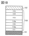
- FIG. 1A to 1E are cross-sectional views showing an example of a light emitting device.
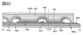
- FIG. 2A is a top view showing an example of a light emitting device.
- 2B and 2C are cross-sectional views showing an example of a light emitting device.
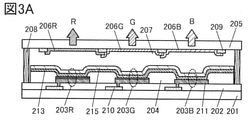
- 3A and 3C are cross-sectional views showing an example of a light emitting device.
- FIG. 3B is a cross-sectional view showing an example of a light emitting device.
- 4A and 4B are cross-sectional views showing an example of a light emitting device.
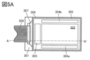
- FIG. 5A is a top view showing an example of a light emitting device.
- FIG. 5B is a cross-sectional view showing an example of a light emitting device.
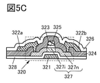
- 5C and 5D are cross-sectional views showing an example of a transistor.
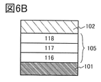
- 6A and 6B are cross-sectional views showing an example of a light receiving device.
- 6C and 6D are views showing an example of a light receiving / receiving device.
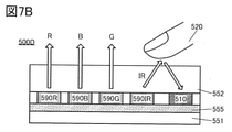
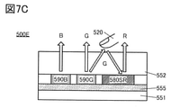
- 7A to 7C are views showing an example of a display device.
- 8A to 8D are views showing an example of an electronic device.
- 9A-9F are views showing an example of an electronic device.
- 10A to 10C are views showing an example of an automobile.
- 11A to 11E are diagrams showing an example of an electronic device.
- FIG. 12 is a cross-sectional view showing the light emitting device of the embodiment.
- FIG. 13 is a diagram showing the measurement results of the refractive indexes of dcPAF and PCBBiF.
- FIG. 14 is a diagram showing the luminance-current density characteristics of the light emitting device of the first embodiment.
- FIG. 15 is a diagram showing the current efficiency-luminance characteristics of the light emitting device of the first embodiment.
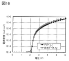
- FIG. 16 is a diagram showing the current density-voltage characteristics of the light emitting device of the first embodiment.
- FIG. 17 is a diagram showing the external quantum efficiency-luminance characteristics of the light emitting device of the first embodiment.
- FIG. 18 is a diagram showing an emission spectrum of the emission device of Example 1.
- FIG. 19 is a diagram showing the results of a reliability test of the light emitting device of Example 1.
- FIG. 20 is a diagram showing the measurement results of the refractive index of mmtBumTPoFBi-04.
- FIG. 21 is a diagram showing the luminance-current density characteristics of the light emitting device of the second embodiment.
- FIG. 22 is a diagram showing the current efficiency-luminance characteristics of the light emitting device of the second embodiment.
- FIG. 23 is a diagram showing the current density-voltage characteristics of the light emitting device of the second embodiment.
- FIG. 24 is a diagram showing the external quantum efficiency-luminance characteristics of the light emitting device of the second embodiment.
- FIG. 25 is a diagram showing an emission spectrum of the emission device of Example 2.
- membrane and the word “layer” can be interchanged with each other in some cases or depending on the situation.
- conductive layer can be changed to the term “conductive layer”.
- insulating film can be changed to the term “insulating layer”.
- the organic EL device can increase the external quantum efficiency by lowering the refractive index of the material used.
- a substituent having a low atomic refraction into the molecule.
- the substituent include a chain-type saturated hydrocarbon group and a cyclic-type saturated hydrocarbon group.
- these substituents interfere with the development of carrier transportability. Therefore, it can be said that it is difficult to achieve both high carrier transportability and low refractive index.
- the glass transition temperature (Tg) of the material used for the organic EL device is high.
- Tg glass transition temperature
- an unsaturated hydrocarbon group particularly a cyclic unsaturated hydrocarbon group
- the refractive index of the material becomes high. As described above, it is difficult to achieve both a high glass transition temperature and a low refractive index.
- TAPC 1,1-bis- (4-bis (4-methyl-phenyl) -amino-phenyl) cyclohexane
- TAPC is a substance that has a perfect balance between carrier transportability and low refractive index.
- TAPC since two bulky substituents are inserted on one carbon of cyclohexane, the steric repulsion becomes large and the molecule itself becomes large. It is disadvantageous in terms of reliability because it induces instability.
- TAPC has a low glass transition temperature of 85 ° C. due to the fact that its skeleton is composed of cyclohexane and a simple benzene ring, and has a problem in heat resistance.
- the hole transporting material has both high carrier transportability and low refractive index, and further improves the glass transition temperature to improve heat resistance, or enhances reliability during driving. It's not easy.
- the present inventors have found an organic compound in which the glass transition temperature is high and the proportion of carbon forming a bond in the sp3 hybrid orbital is within a certain range. Then, they have found a configuration of a light emitting device having high luminous efficiency and low driving voltage using the layer containing the organic compound.
- one aspect of the present invention is a first electrode, a first layer on the first electrode, a second layer on the first layer, and a light emitting layer on the second layer. And a second electrode on the light emitting layer, the light emitting device.
- the first layer has a first organic compound and the second layer has a second organic compound.
- the ratio of the number of carbon atoms forming a bond in the sp3 hybrid orbital to the total number of carbon atoms of the first organic compound is 23% or more and 55% or less.
- the second organic compound contains fluorine.
- one embodiment of the present invention comprises a first electrode, a first layer on the first electrode, a second layer on the first layer, a light emitting layer on the second layer, and light emission.
- a light emitting device having a second electrode on the layer.
- the first layer has a first organic compound and the second layer has a second organic compound.
- the glass transition temperature of the first organic compound is 90 ° C. or higher.
- the refractive index of the layer made of the first organic compound in light having a wavelength of 633 nm is 1.45 or more and 1.70 or less.
- the second organic compound contains fluorine.
- one embodiment of the present invention comprises a first electrode, a first layer on the first electrode, a second layer on the first layer, a light emitting layer on the second layer, and light emission.
- a light emitting device having a second electrode on the layer.
- the first layer has a first organic compound and the second layer has a second organic compound.
- the first organic compound is a monoamine compound.
- the refractive index of the layer made of the first organic compound in light having a wavelength of 633 nm is 1.45 or more and 1.70 or less.
- the second organic compound contains fluorine.
- the first organic compound is a substituent (one or both of a chain saturated hydrocarbon group and a cyclic saturated hydrocarbon group) composed of carbon forming a bond in an sp3 hybrid orbital in order to lower the refractive index. ).
- substituents are often bulky, and as a result, the first layer is prone to carrier injection barriers (here, hole injection barriers) with adjacent layers.
- a second layer containing a second organic compound is provided between the first layer and the light emitting layer.
- the second organic compound exhibits electron acceptability with respect to the first organic compound. Therefore, an interaction occurs between the first organic compound and the second organic compound, and a charge transfer complex is formed. This facilitates hole injection from the first layer into the light emitting layer.
- the second layer is provided in contact with the first layer.
- the first layer is prone to hole injection barriers with adjacent layers. The barrier can be reduced by configuring the first layer and the second layer to be in contact with each other.
- the second layer may contain both the second organic compound and the third organic compound.
- the second organic compound preferably exhibits electron acceptability with respect to the third organic compound. Then, it is preferable that an interaction occurs between the second organic compound and the third organic compound to form a charge transfer complex. This facilitates hole injection from the first layer into the light emitting layer.
- the second organic compound preferably exhibits electron acceptability for both the first organic compound and the third organic compound. Then, it is preferable that the second organic compound interacts with at least one of the first organic compound and the third organic compound to form a charge transfer complex. This facilitates hole injection from the first layer into the light emitting layer.
- the refractive index of the layer made of the first organic compound is preferably lower than the refractive index of the layer made of the third organic compound.
- the difference between the refractive index of the layer made of the first organic compound in light having a wavelength of 633 nm and the refractive index of the layer made of the third organic compound in light having a wavelength of 633 nm is 0.05 or more. It is preferably 0.1 or more, more preferably 0.15 or more, and even more preferably 0.15 or more.
- the second organic compound includes an organic compound containing fluorine, and an organic compound containing a cyano group is preferable.
- the lowest unoccupied molecular orbital (LUMO) level of the second organic compound is preferably ⁇ 5.0 eV or less.
- the second organic compound When the second organic compound emits light, the light emitted by the light emitting substance contained in the light emitting layer is reduced, so that the luminous efficiency of the light emitting device is lowered. Therefore, it is preferable that no light emission from the second organic compound is observed.
- the hole injection barrier becomes particularly high and drives.
- the voltage tends to be high.
- the second layer between the first layer and the light emitting layer it is possible to facilitate hole transportation from the first layer to the light emitting layer and lower the drive voltage of the light emitting device. can.
- the third organic compound a hole transporting material and an electron blocking material can be used.
- the third organic compound has both hole transporting property and electron blocking property.
- the third organic compound preferably has low electron injecting property and electron transporting property.
- the HOMO level of the third organic compound is preferably lower than the HOMO level of the first organic compound. Further, it is preferable that the LUMO level of the third organic compound is higher than the LUMO level of the material having the lowest LUMO level among the materials contained in the light emitting layer.
- the light emitting device of one aspect of the present invention may have a third layer between the second layer and the light emitting layer.
- the third layer has a third organic compound.
- the third layer is preferably in contact with the second layer.
- the higher the HOMO level of the third organic compound the lower the drive voltage of the light emitting device.
- the HOMO level of the third organic compound is high, an excited complex is formed between the third organic compound and the host material of the light emitting layer. It becomes easy to form, and there is a risk that the light emission efficiency will decrease.
- the HOMO level of the third organic compound is lowered, the luminous efficiency can be increased, but the hole injection barrier between the first layer and the third layer becomes high, and the driving voltage becomes high.
- the first organic compound has a substituent that inhibits carrier transportability, such as a saturated hydrocarbon group that does not have a ⁇ orbital, the carrier injection property into the third organic compound is significantly lowered, and the light emitting device.
- the drive voltage of is high.
- a second layer containing a second organic compound is provided between the first layer and the third layer.
- the HOMO level of the third organic compound is low, hole transportation from the first layer to the light emitting layer can be smoothed, and both high luminous efficiency of the light emitting device and low driving voltage can be achieved. Can be done.
- an organic compound having a low refractive index but poor carrier injection property is used for the first layer, hole transport from the first layer to the light emitting layer can be facilitated, and the high luminous efficiency of the light emitting device can be achieved. And low drive voltage can be achieved at the same time.
- the third layer may have both a second organic compound and a third organic compound.
- the above configuration can be applied not only to a light emitting device but also to a light receiving device such as an organic photodiode, and a light receiving / receiving device having both light emitting and light receiving functions.
- the light emitting device of one aspect of the present invention may further have a fourth layer between the first electrode and the first layer.
- the fourth layer has a first organic compound and a second organic compound.
- a composite material having the first organic compound and the second organic compound described above can be used.
- the composite material can be used for a hole injection layer, a hole transport layer, a charge generation layer, and the like in a light emitting device.
- the composite material can be used as a carrier transporting material (hole transporting material) in a light receiving device, a light receiving and receiving device, and the like.
- a composite material containing a hole transporting material and a material having electron acceptability for the hole transporting material is used, respectively. Can be done.
- these layers In order for these layers to have a hole-injecting property or a charge-generating function, it is necessary that an interaction occurs between the materials constituting the composite material to form a charge transfer complex.
- the composite material contains a large amount of a material having electron acceptability, light absorption in the visible region may occur, and the luminous efficiency of the organic EL device may decrease. Therefore, it is preferable that the composite material contains more hole-transporting materials than the material having electron acceptability.
- a composite material in which a material having electron acceptability is added in a small amount to the hole transporting material can be used.
- the refractive index of the composite material is also low. If the refractive index of the first organic compound, which occupies most of the composite material, is low, the refractive index of the composite material can be lowered.
- the ratio of the number of carbon atoms forming the bond in the sp3 hybrid orbital to the total number of carbon atoms of the first organic compound is preferably 23% or more and 55% or less.
- the substituent composed of carbon forming a bond in the sp3 hybrid orbital is a so-called chain-type saturated hydrocarbon group or a cyclic-type saturated hydrocarbon group, and therefore has low atomic refraction. Therefore, the refractive index of the first organic compound can be lowered.
- the glass transition temperature of the first organic compound is preferably 90 ° C. or higher, more preferably 95 ° C. or higher, more preferably 100 ° C. or higher, further preferably 110 ° C. or higher, still more preferably 120 ° C. or higher.
- the first organic compound can maintain a high glass transition temperature and can be a material having high heat resistance.
- the introduction of saturated hydrocarbon groups, especially chain saturated hydrocarbon groups results in at least one of the glass transition temperature and melting point of the compound compared to the corresponding aromatic or heteroaromatic group (eg, having the same number of carbon atoms). Tends to go down.
- the glass transition temperature decreases, the heat resistance of the organic EL material may decrease. Since it is desirable that various devices using organic EL materials exhibit stable physical properties under various usage environments, it is preferable that the materials exhibiting the same characteristics have a high glass transition temperature.
- the refractive index of the layer made of the first organic compound in light having a wavelength of 633 nm is preferably 1.45 or more and 1.70 or less.
- 633 nm is a wavelength usually used for measuring the refractive index.
- the refractive index in the wavelength (455 nm or more and 465 nm or less) of the blue light emitting region of the layer made of the first organic compound is preferably 1.50 or more and 1.75 or less.
- the refractive index in the wavelength (525 nm or more and 535 nm or less) of the green light emitting region of the layer made of the first organic compound is preferably 1.48 or more and 1.73 or less.
- the refractive index for normal light and the refractive index for abnormal light may differ.
- anisotropy analysis it is possible to calculate the refractive index of each of the normal light refractive index and the abnormal light refractive index separately.
- the normal light refractive index is used as an index.
- the refractive index of the layer made of the first organic compound As the refractive index of the layer made of the first organic compound, the refractive index at the peak wavelength of the light emitted by the light emitting device in which the first organic compound is used or the emission peak wavelength of the light emitting substance contained in the light emitting device is used. It may be used to evaluate the first organic compound. Also in this case, the refractive index of the layer made of the first organic compound is preferably 1.50 or more and 1.75 or less, 1.48 or more and 1.73 or less, or 1.45 or more and 1.70 or less. .. When a structure for adjusting light such as a color filter is provided, the peak wavelength of the light emitted by the light emitting device is the peak wavelength of the light before passing through the structure.
- the emission peak wavelength of the luminescent substance is calculated from the PL spectrum in the solution state. Since the relative permittivity of the organic compound constituting the EL layer of the light emitting device is about 3, the relative permittivity of the solvent for putting the light emitting center substance into a solution state is set in order to avoid a discrepancy with the light emitting spectrum of the light emitting device. , 1 or more and 10 or less, more preferably 2 or more and 5 or less at room temperature. Specific examples of the solution include hexane, benzene, toluene, diethyl ether, ethyl acetate, chloroform, chlorobenzene, and dichloromethane. Further, as the solution, a general-purpose solvent having a relative permittivity of 2 or more and 5 or less at room temperature and high solubility is more preferable. As the solution, for example, toluene or chloroform is preferably used.
- the first organic compound is preferably an amine compound, more preferably a monoamine compound, and even more preferably a triaryl monoamine compound.
- the first organic compound is an amine compound because it is easy to control the HOMO level to a desired height depending on the substitution position of the alkyl group.
- the first organic compound preferably has an alkyl group bonded to the same plane as or in the vicinity of the plane forming HOMO. That is, it is preferable to arrange the alkyl group at a position where the HOMO is not shielded.
- the plane forming the HOMO includes the plane of the aromatic ring to which nitrogen is bonded.
- the alkyl group is preferably a tert-butyl group or a cyclohexyl group.
- the first organic compound preferably has an alkyl group that functions as an electron donating group at a bond position that further destabilizes the energy of HOMO.
- an alkyl group at the para position of the nitrogen atom of triphenylamine. This makes it possible to raise (shallow) the HOMO level of the first organic compound.
- the first organic compound preferably has a skeleton having a high carrier transport property, and the aromatic amine skeleton is a preferable skeleton having a high hole transport property.
- the diamine structure may adversely affect reliability depending on the substituents arranged around the TAPC as described above.
- the monoamine compound is a material having the same good reliability as a conventional hole transporting material having a normal refractive index.
- better characteristics can be obtained by devising at least one of the number of substituents and the substitution position of the substituent (alkyl group, cycloalkyl group, etc.) having carbon forming a bond in the sp3 hybrid orbital of the monoamine compound.
- the stability of the molecule can be improved by limiting the number of aromatic groups bonded to the saturated hydrocarbon group and reducing the steric repulsion. From this, it is possible to obtain an optical device having a good life.
- the molecular weight of the first organic compound is preferably 650 or more and 1200 or less. This makes it possible to increase the heat resistance of the first organic compound.
- the integrated value of the signal of less than 4 ppm is preferably larger than the integrated value of the signal of 4 ppm or more.
- Signals less than 4 ppm reflect hydrogen in chain or cyclic saturated hydrocarbon groups, which is greater than the integral of signals above 4 ppm means that the number of hydrogen atoms that make up the saturated hydrocarbon groups is unsaturated. It means that there are more hydrogen atoms that make up hydrocarbons. From this, the ratio of sp3 carbon in the molecule can be estimated.
- the carbon of the unsaturated hydrocarbon group has fewer bonds that can be bonded to hydrogen, and when compared with benzene and cyclohexane, for example, there is a difference between C 6 H 6 and C 6 H 12 .
- the fact that the integral value of a signal of less than 4 ppm is larger than the integral value of a signal of 4 ppm or more in the result of measurement by 1 H-NMR means that, among the carbons constituting the molecule, It shows that about one-third of the carbon atoms participating in the saturated hydrocarbon group are present.
- the first organic compound becomes an organic compound having a low refractive index, and can be suitably used as a hole transporting material.
- the first organic compound has a first aromatic group, a second aromatic group, and a third aromatic group, and has a first aromatic group, a second aromatic group, and a second aromatic group.
- Examples thereof include monoamine compounds in which the third aromatic group is directly bonded to the same nitrogen atom.
- the monoamine compound has at least one fluorene skeleton because it has good hole transportability. Therefore, it is preferable that any one or more of the above-mentioned first aromatic group, second aromatic group, and third aromatic group is a fluorene skeleton. Further, the fact that the fluorene skeleton is directly bonded to the nitrogen atom of the amine contributes to raising the HOMO level of the molecule and facilitates the transfer of holes.
- the first aromatic group and the second aromatic group each independently have 1 or more and 3 or less benzene rings. Moreover, it is preferable that both the first aromatic group and the second aromatic group are hydrocarbon groups. That is, it is preferable that the first aromatic group and the second aromatic group are a phenyl group, a biphenyl group, a terphenyl group, or a naphthylphenyl group, respectively. It is preferable that the first aromatic group or the second aromatic group is a terphenyl group because the glass transition temperature is improved and the heat resistance is improved.
- first aromatic group and the second aromatic group each have 2 or 3 benzene rings
- the 2 or 3 benzene rings are bonded to each other.
- one or both of the first aromatic group and the second aromatic group are substituents in which two or three benzene rings are bonded to each other, that is, a biphenyl group or a terphenyl group, the glass transition temperature. It is preferable that the first aromatic group and the second aromatic group are independently biphenyl groups or terphenyl groups, respectively.
- first aromatic group and the second aromatic group have one or more hydrocarbon groups having 1 or more and 12 or less carbon atoms in which carbon forms a bond only in the sp3 hybrid orbital. Is preferable.
- hydrocarbon group an alkyl group having 3 or more and 8 or less carbon atoms and a cycloalkyl group having 6 or more and 12 or less carbon atoms are preferable.
- the total amount of carbon contained in the above-mentioned hydrocarbon group bonded to the first aromatic group or the second aromatic group is 6 or more. Moreover, the total amount of carbon contained in all the above-mentioned hydrocarbon groups bonded to the first aromatic group and the second aromatic group is 8 or more, preferably 12 or more.
- the total amount of carbon contained in all the above-mentioned hydrocarbon groups bonded to the first aromatic group and the second aromatic group is preferably 36 or less, preferably 30 or less, in order to maintain good carrier transportability. More preferred.
- the third aromatic group is a substituted or unsubstituted monocycle, or a substituted or unsubstituted fused ring of 3 or less. As the number of fused rings increases, the refractive index tends to increase. Further, as the number of fused rings increases, one or both of absorption and emission of light in the visible region can be observed. Therefore, by setting the number of fused rings to 3 or less, it is possible to maintain a low refractive index and to obtain a material having a small influence of absorption and light emission.
- the third aromatic group preferably has 6 or more and 13 or less carbon atoms forming a ring in order to maintain a low refractive index.
- the third aromatic group examples include a benzene ring, a naphthalene ring, a fluorene ring, and an acenaphthylene ring.
- the third aromatic group preferably contains a fluorene ring, and more preferably a fluorene ring.
- an organic compound represented by the general formula (G1) to the general formula (G4) can be used as the first organic compound.
- the organic compound represented by the general formula (G1) to the general formula (G4) can be said to be an example of a monoamine compound and an example of a triarylmonoamine compound.
- Ar 1 and Ar 2 each independently represent a substituted or unsubstituted benzene ring, or a substituent in which two or three substituted or unsubstituted benzene rings are bonded to each other. ..
- Ar 1 and Ar 2 have one or more hydrocarbon groups having 1 or more and 12 or less carbon carbons forming a bond only in the sp3 hybrid orbital, and Ar 1 and Ar 2 have one or more carbon groups.
- the total amount of carbon contained in all the bonded hydrocarbon groups is 8 or more, and the total amount of carbon contained in all the hydrocarbon groups bonded to either Ar 1 or Ar 2 is 6 or more.
- R 1 to R 3 independently represent an alkyl group having 1 or more and 4 or less carbon atoms, and u represents an integer of 0 or more and 4 or less.
- R 1 and R 2 may be bonded to each other to form a ring.
- Ar 1 and Ar 2 include substituted or unsubstituted phenyl group, biphenyl group, terphenyl group, naphthylphenyl group and the like.
- an alkyl group having 3 to 8 carbon atoms and a cycloalkyl group having 6 to 12 carbon atoms are preferable. .. Specifically, propyl group, isopropyl group, butyl group, sec-butyl group, isobutyl group, tert-butyl group, pentyl group, isopentyl group, sec-pentyl group, tert-pentyl group, neopentyl group, hexyl group, isohexyl.
- linear alkyl groups having 1 or 2 carbon atoms When a plurality of linear alkyl groups having 1 or 2 carbon atoms are bonded to Ar 1 or Ar 2 as hydrocarbon groups, the linear alkyl groups may be bonded to each other to form a ring.
- n, m, p, and r independently represent 1 or 2, and s, t, and u each independently represent an integer of 0 or more and 4 or less. Further, n + p and m + r are independently 2 or 3, respectively.
- R 1 to R 3 independently represent an alkyl group having 1 or more and 4 or less carbon atoms
- R 4 and R 5 each independently represent hydrogen or a hydrocarbon group having 1 or more and 3 or less carbon atoms.
- R 10 to R 14 and R 20 to R 24 respectively, independently represent a hydrocarbon group having 1 or more and 12 or less carbon atoms in which hydrogen or carbon forms a bond only in the sp3 hybrid orbital.
- the total amount of carbon contained in R10 to R14 and R20 to R24 is 8 or more, and the total amount of carbon contained in either R10 to R14 or R20 to R24 is 6 . That is all.
- R 1 and R 2 may be bonded to each other to form a ring, and in R 4 , R 5 , R 10 to R 14 , and R 20 to R 24 , adjacent groups are bonded to each other to form a ring. It may be formed.
- n and p each independently represent 1 or 2, and s and u each independently represent an integer of 0 or more and 4 or less. Further, n + p is 2 or 3.
- R 1 to R 3 independently represent an alkyl group having 1 or more and 4 or less carbon atoms
- R 4 represents hydrogen or a hydrocarbon group having 1 or more and 3 or less carbon atoms
- R 10 to R 14 and R 20 to R 24 each independently represent a hydrocarbon group having 1 or more and 12 or less carbon atoms in which hydrogen or carbon forms a bond only in the sp3 hybrid orbital.
- the total amount of carbon contained in R10 to R14 and R20 to R24 is 8 or more, and the total amount of carbon contained in either R10 to R14 or R20 to R24 is 6 . That is all.
- R 1 and R 2 may be bonded to each other to form a ring, and in R 4 , R 10 to R 14 and R 20 to R 24 , adjacent groups are bonded to each other to form a ring. You may be doing it.
- examples of the hydrocarbon group having 1 or more and 3 or less carbon atoms include a methyl group, an ethyl group, and a propyl group.
- examples of the hydrocarbon group having 1 or more and 4 or less carbon atoms include a butyl group in addition to the above.
- s, t, and u are independently 0. Further, when s is an integer of 2 or more and 4 or less, the plurality of R 4s may be the same or different, and when t is an integer of 2 or more and 4 or less, the plurality of R 5s are the same. However, when u is an integer of 2 or more and 4 or less, the plurality of R 3s may be the same or different.
- u represents an integer of 0 or more and 4 or less
- R 1 to R 3 independently represent an alkyl group having 1 or more and 4 or less carbon atoms, and R 10 to R 14 and R 20 respectively.
- R 24 each independently represent a hydrocarbon group having 1 or more and 12 or less carbon atoms in which hydrogen or carbon forms a bond only in the sp3 hybrid orbital.
- the total amount of carbon contained in R10 to R14 and R20 to R24 is 8 or more, and the total amount of carbon contained in either R10 to R14 or R20 to R24 is 6 . That is all.
- R 1 and R 2 may be bonded to each other to form a ring, and in R 10 to R 14 and R 20 to R 24 , adjacent groups are bonded to each other to form a ring. May be good.
- u is preferably 0. Further, when u is an integer of 2 or more and 4 or less, the plurality of R 3s may be the same or different.
- R 10 to R 14 and R 20 to R 24 are independently any of hydrogen, tert-butyl group, and cyclohexyl group, the refractive index is determined. It is preferable because it can be lowered. Further, it is preferable that at least three of R 10 to R 14 and at least three of R 20 to R 24 are hydrogen because the carrier transport property is not easily impaired.
- an arylamine compound having at least one aromatic group, the aromatic group having a first to third benzene ring and at least three alkyl groups is used. Can be mentioned. It is assumed that the first to third benzene rings are bonded in this order, and the first benzene ring is directly bonded to the nitrogen atom of the amine.
- the first benzene ring may further have a substituted or unsubstituted phenyl group, and preferably has an unsubstituted phenyl group. Further, the second benzene ring or the third benzene ring may have a phenyl group substituted with an alkyl group.
- first to third benzene rings two or more benzene rings, preferably the carbons at the 1st and 3rd positions of all the benzene rings, are not directly bonded to hydrogen, and the above-mentioned first benzene ring is not directly bonded. It is assumed that it is bonded to any of the third benzene ring, the phenyl group substituted with the above-mentioned alkyl group, the above-mentioned at least three alkyl groups, and the above-mentioned amine nitrogen atom.
- the arylamine compound further has a second aromatic group.
- the second aromatic group is preferably an unsubstituted monocycle or a group having a substituted or unsubstituted 3 or less fused ring, and more particularly a substituted or unsubstituted 3 or less fused ring.
- the fused ring is more preferably a group having a fused ring having 6 or more and 13 or less carbons forming the ring, and further preferably a group having a fluorene ring.
- the dimethylfluorenyl group is preferable as the second aromatic group.
- the arylamine compound preferably further has a third aromatic group.
- the third aromatic group has 1 or more and 3 or less substituted or unsubstituted benzene rings, respectively.
- the above-mentioned alkyl group substituting at least three alkyl groups and phenyl groups is preferably a chain alkyl group having 2 or more and 5 or less carbon atoms, and a chain alkyl group having a branch having 3 or more and 5 or less carbon atoms is more preferable. Preferred, a tert-butyl group is even more preferred.
- an organic compound represented by the general formula (G11) to the general formula (G13) can be used as the first organic compound.
- the organic compound represented by the general formula (G11) to the general formula (G13) can be said to be an example of a monoamine compound and an example of a triarylmonoamine compound.
- Ar 101 represents a substituted or unsubstituted benzene ring, or a substituent in which two or three substituted or unsubstituted benzene rings are bonded to each other
- R 106 to R 108 are Each independently represents an alkyl group having 1 or more and 4 or less carbon atoms
- v represents an integer of 0 or more and 4 or less
- one of R 111 to R 115 represents a substituent represented by the general formula (g1).
- Others independently represent hydrogen, an alkyl group having 1 or more and 6 or less carbon atoms, and any one of a substituted or unsubstituted phenyl group.
- the number of substituted or unsubstituted phenyl groups in R 111 to R 115 is 1 or less. Moreover, it is preferable that the phenyl group is unsubstituted.
- the substituent is an alkyl group having 1 or more and 6 or less carbon atoms.
- Ar 101 include substituted or unsubstituted phenyl group, biphenyl group, terphenyl group, naphthylphenyl group and the like.
- the plurality of R 108s may be the same or different.
- one of R 121 to R 125 represents a substituent represented by the general formula (g2), and the other is independently hydrogen and an alkyl group having 1 or more and 6 or less carbon atoms.
- R 131 to R 135 each independently contain any one of hydrogen, an alkyl group having 1 or more and 6 or less carbon atoms, and a phenyl group substituted with an alkyl group having 1 or more and 6 or less carbon atoms. show.
- R 111 to R 115 , R 121 to R 125 , and R 131 to R 135 at least three or more are alkyl groups having 1 or more and 6 or less carbon atoms.
- the organic compound represented by the above general formula (G11) can be made into an arylamine compound having a low refractive index.
- the number of phenyl groups substituted with an alkyl group having 1 or more and 6 or less carbon atoms in R 121 to R 125 and R 131 to R 135 is one or less, that is, carbon in R 121 to R 125 and R 131 to R 135 . It is assumed that the phenyl group substituted with an alkyl group having a number of 1 or more and 6 or less is 1 or 0.
- R 112 and R 114 In addition, in at least two combinations of the three combinations of R 112 and R 114 , R 122 and R 124 , and R 132 and R 134 , it is assumed that at least one R is other than hydrogen. That is, among the benzene rings having R 112 and R 114 , the benzene rings having R 122 and R 124 , and the benzene rings having R 132 and R 134 , in two or more benzene rings, the carbon at the meta position of each has carbon. At least one of them is not hydrogen, that is, it has a substituent. At this time, it is preferable that at least one of R 112 , R 114 , R 122 , and R 124 is other than hydrogen, and at least one of R 132 and R 134 is other than hydrogen.
- alkyl group having 1 or more and 4 or less carbon atoms examples include a methyl group, an ethyl group, a propyl group, an isopropyl group, a butyl group, a sec-butyl group, an isobutyl group and the like, and a tert-butyl group is particularly preferable. ..
- an alkyl group having 1 or more and 6 or less carbon atoms and a cycloalkyl group having 5 or more and 12 or less carbon atoms can be used as the substituent.
- the alkyl group having 1 to 6 carbon atoms is preferably a chain alkyl group having 2 or more carbon atoms from the viewpoint of lowering the refractive index, and a chain alkyl group having 5 or less carbon atoms is preferable from the viewpoint of ensuring carrier transportability. .. Further, the effect of reducing the refractive index is remarkable in the chain alkyl group having a branch having 3 or more carbon atoms. That is, the alkyl group having 1 or more and 6 or less carbon atoms is preferably a chain-type alkyl group having 2 or more and 5 or less carbon atoms, and more preferably a chain-type alkyl group having a branch having 3 or more and 5 or less carbon atoms.
- alkyl group having 1 or more and 6 or less carbon atoms examples include a methyl group, an ethyl group, a propyl group, an isopropyl group, a butyl group, a sec-butyl group, an isobutyl group, a tert-butyl group, a pentyl group, and a hexyl group.
- the tert-butyl group is particularly preferred.
- Examples of the cycloalkyl group having 5 or more and 12 or less carbon atoms include a cyclohexyl group, a 4-methylcyclohexyl group, a cycloheptyl group, a cyclooctyl group, a cyclononyl group, a cyclodecyl group, a decahydronaphthyl group, a cycloundecyl group, and a cyclododecyl group.
- a cycloalkyl group having 6 or more carbon atoms is preferable for lowering the refractive index, and a cyclohexyl group and a cyclododecyl group are particularly preferable.
- the general formula (G12) is an example in the general formula (G11) in which Ar 101 is a substituent in which two or three substituted or unsubstituted benzene rings are bonded to each other. Therefore, the description of the part similar to the general formula (G11) may be omitted.
- R 106 to R 109 each independently represent an alkyl group having 1 or more and 4 or less carbon atoms
- v and w each independently represent an integer of 0 or more and 4 or less
- x and y independently represents 1 or 2
- x + y is 2 or 3. Both x and y are preferably 1.
- R 141 to R 145 independently represent hydrogen, an alkyl group having 1 or more and 6 or less carbon atoms, and a cycloalkyl group having 5 or more and 12 or less carbon atoms.
- the plurality of R 108s may be the same or different.
- the plurality of R 109s may be the same or different.
- the types of substituents of the two phenylene groups, the number of substituents, and the positions of the binding hands may be the same or different.
- the types of substituents of the two phenyl groups and the number of substituents may be the same or different.
- the general formula (G13) is an example in the general formula (G11) in which Ar 101 is a single substituted or unsubstituted benzene ring. Therefore, the description of the part similar to the general formula (G11) may be omitted.
- R 101 to R 105 are independently hydrogen, an alkyl group having 1 or more and 6 or less carbon atoms, a cycloalkyl group having 6 or more and 12 or less carbon atoms, and a substituted or unsubstituted phenyl group. Represents any one of.
- R 101 to R 105 it is preferable that R 103 is a cyclohexyl group and the rest are all hydrogen. Further, among R 101 to R 105 , it is preferable that R 101 is an unsubstituted phenyl group and the rest is hydrogen, because the hole transport property is improved.
- organic compound that can be used as the first organic compound include N, N-bis (4-cyclohexylphenyl) -9,9-dimethyl-9H-fluoren-2-amine (abbreviation: dchPAF). , N-[(3', 5'-ditersary butyl) -1,1'-biphenyl-4-yl] -N- (4-cyclohexylphenyl) -9,9-dimethyl-9H-fluoren-2-amine (Abbreviation: mmtBuBichPAF), N- (3,3'', 5,5''-tetra-t-butyl-1,1': 3', 1''-terphenyl-5'-yl) -N- (4-Cyclohexylphenyl) -9,9-dimethyl-9H-fluoren-2-amine (abbreviation: mmtBumTPchPAF), N-[(3,3', 5'-t-buty
- the second organic compound contains fluorine.
- the second organic compound is particularly preferably containing a cyano group.
- the second organic compound preferably exhibits electron acceptability with respect to the first organic compound.
- the LUMO level of the second organic compound is preferably ⁇ 5.0 eV or less.
- the second organic compound examples include 7,7,8,8-tetracyano-2,3,5,6-tetrafluoroquinodimethane (abbreviation: F4 - TCNQ), 1,3,4. , 5,7,8-Hexafluorotetracyano-naphthoquinodimethane (abbreviation: F6-TCNNQ), 2- (7-dicyanomethylene-1,3,4,5,6,8,9,10-octafluoro -7H-pyrene-2-iriden) malononitrile and the like can be mentioned.
- the [3] radialene derivative having an electron-withdrawing group is preferable because it has very high electron acceptability, and specifically, ⁇ , ⁇ ', ⁇ ''-.
- 1,2,3-Cyclopropanetriylidentris [4-cyano-2,3,5,6-tetrafluorobenzenitrile], ⁇ , ⁇ ', ⁇ ''-1,2,3-cyclopropanetriiridentris [2,6-dichloro-3,5-difluoro-4- (trifluoromethyl) benzenenitrile acetonitrile] and ⁇ , ⁇ ', ⁇ ''-1,2,3-cyclopropanetriylidentris [2,3 , 4, 5, 6-Pentafluorobenzene acetonitrile] and the like.
- the second organic compound does not contain a metal element because it facilitates vapor deposition.
- the third organic compound when used for the light emitting device of one aspect of the present invention, it is preferable that the second organic compound exhibits electron acceptability with respect to the third organic compound.
- a composite material of the first organic compound and the second organic compound can be used for the light emitting device of one aspect of the present invention.
- the mass percent concentration of the second organic compound in the composite material is preferably 10 wt% or less, more preferably 5 wt% or less.
- the volume percent concentration of the second organic compound in the composite material is preferably 10 vol% or less, more preferably 5 vol% or less, still more preferably 3 vol% or less.
- the third organic compound a hole transporting material and an electron blocking material can be used.
- the third organic compound has both hole transporting property and electron blocking property.
- the hole transporting materials described later it is preferable to use a material having an electron blocking property.
- the third organic compound preferably has low electron injecting property and electron transporting property.
- the HOMO level of the third organic compound is preferably lower than the HOMO level of the first organic compound.
- the HOMO level of the third organic compound is preferably ⁇ 5.40 eV or less.
- the LUMO level of the third organic compound is higher than the LUMO level of the material having the lowest LUMO level among the materials contained in the light emitting layer.
- the LUMO level of the third organic compound is preferably -2.50 eV or higher.
- the third organic compound a compound that can be used for the first organic compound can be used. Further, as the third organic compound, a hole transporting material described later can be used.
- the refractive index of the layer made of the first organic compound is preferably lower than the refractive index of the layer made of the third organic compound.
- the difference between the refractive index of the layer made of the first organic compound in light having a wavelength of 633 nm and the refractive index of the layer made of the third organic compound in light having a wavelength of 633 nm is 0.05 or more. It is preferably 0.1 or more, more preferably 0.15 or more, and even more preferably 0.15 or more.
- the refractive index of the layer made of the third organic compound in light having a wavelength of 633 nm is preferably 1.45 or more and 1.70 or less.
- the refractive index in the wavelength (525 nm or more and 535 nm or less) of the green light emitting region of the layer made of the third organic compound is preferably 1.48 or more and 1.73 or less.
- the refractive index in the wavelength (455 nm or more and 465 nm or less) of the blue light emitting region of the layer made of the third organic compound is preferably 1.50 or more and 1.75 or less.
- the ratio of the number of carbon atoms forming the bond in the sp3 hybrid orbital to the total number of carbon atoms of the third organic compound is preferably 23% or more and 55% or less.
- the substituent composed of carbon forming a bond in the sp3 hybrid orbital is a so-called chain-type saturated hydrocarbon group or a ring-type saturated hydrocarbon group, and therefore has low atomic refraction. Therefore, the refractive index of the third organic compound can be lowered.
- the glass transition temperature of the third organic compound is preferably 90 ° C. or higher, more preferably 95 ° C. or higher, more preferably 100 ° C. or higher, further preferably 110 ° C. or higher, still more preferably 120 ° C. or higher.
- the third organic compound is preferably an amine compound, more preferably a monoamine compound, and even more preferably a triaryl monoamine compound.
- the molecular weight of the third organic compound is preferably 650 or more and 1200 or less. This makes it possible to increase the heat resistance of the first organic compound.
- the integrated value of the signal of less than 4 ppm is preferably larger than the integrated value of the signal of 4 ppm or more.
- the above description of the first organic compound can be referred to.
- the light emitting device shown in FIG. 1A has a structure (single structure) in which the EL layer 103 is sandwiched between the first electrode 101 and the second electrode 102.
- the EL layer 103 has at least a light emitting layer.
- the EL layer 103 further includes one or more of various layers such as a hole injection layer, a hole transport layer, an electron transport layer, an electron injection layer, a carrier block layer, an exciton block layer, and a charge generation layer. Can have a layer of.
- FIG. 1B shows an example of the laminated structure of the EL layer 103.
- the EL layer 103 has a hole injection layer 111, a first hole transport layer 112a, a buffer layer 119, a second hole transport layer 112b, a light emitting layer 113, and an electron transport layer 114 on the first electrode 101. It also has a structure in which the electron injection layers 115 are sequentially laminated.
- the hole injection layer 111, the first hole transport layer 112a, the buffer layer 119, the second hole transport layer 112b, the light emitting layer 113, the electron transport layer 114, and the electron injection layer 115 each have a single layer structure. It may be present or may have a laminated structure. When the first electrode 101 is a cathode and the second electrode 102 is an anode, the stacking order is reversed.
- the above-mentioned first layer can be used as the first hole transport layer 112a, and the above-mentioned second layer can be used as the buffer layer 119. Further, it is preferable to use the above-mentioned third layer as the second hole transport layer 112b. Further, it is preferable to use the above-mentioned fourth layer as the hole injection layer 111.
- the organic compound used for the buffer layer 119 and the organic compound used for the second hole transport layer 112b may be mixed. Further, the organic compound used for the buffer layer 119 may be added to the second hole transport layer 112b without providing the buffer layer 119. Alternatively, the organic compound used for the second hole transport layer 112b may be added to the buffer layer 119 without providing the second hole transport layer 112b.
- the light emitting device may have a plurality of EL layers between the pair of electrodes.
- the light emitting device has an EL layer of n layers (n is an integer of 2 or more), and has a charge generation layer 104 between the EL layer of the (n-1) th layer and the EL layer of the nth layer. Is preferable.
- FIG. 1C shows a light emitting device having a tandem structure having two EL layers (EL layers 103a and 103b) between a pair of electrodes. Further, FIG. 1D shows a light emitting device having a tandem structure having three EL layers (EL layers 103a, 103b, 103c).
- Each of the EL layers 103a, 103b, and 103c has at least a light emitting layer.
- the same laminated structure as the EL layer 103 shown in FIG. 1B can be applied to at least one EL layer.
- the same laminated structure as the EL layer 103 shown in FIG. 1B to the EL layer exhibiting green phosphorescent emission, it is possible to achieve both high luminous efficiency and low drive voltage, which is preferable.
- the EL layers 103a, 103b, and 103c are the hole injection layer 111, the first hole transport layer 112a, the buffer layer 119, the second hole transport layer 112b, the electron transport layer 114, and the electron injection layer 115, respectively. It can have one or more layers of them.
- the charge generation layer 104 transmits visible light or near-infrared light from the viewpoint of light extraction efficiency (specifically, the transmittance of the visible light or near-infrared light of the charge generation layer 104 is 40. % Or more) is preferable. Further, the charge generation layer 104 functions even if the conductivity is lower than that of one or both of the first electrode 101 and the second electrode 102.
- the EL layers are provided in contact with each other and the same configuration as that of the charge generation layer 104 is formed between the two, the EL layers can be provided in contact with each other without the charge generation layer. For example, when a charge generation region is formed on one surface of the EL layer, the EL layer can be provided in contact with the surface.
- the tandem structure light emitting device has higher current efficiency than the single structure device, and requires less current to illuminate with the same brightness. Therefore, the life of the light emitting device is long, and the reliability of the light emitting device and the electronic device can be improved.
- the light emitting layer 113 has a light emitting substance and another substance in an appropriate combination, and can be configured to obtain fluorescent light emission or phosphorescent light emission having a desired wavelength. Further, the light emitting layer 113 may have a laminated structure having different emission wavelengths. In this case, different materials can be used for the luminescent substance and other substances used for each of the laminated light emitting layers. Further, the EL layers 103a, 103b, 103c shown in FIGS. 1C and 1D may be configured to emit light having different wavelengths from each other. In this case as well, the luminescent substance and other substances used for each light emitting layer can be made of different materials. For example, in FIG.
- the EL layer 103a by configuring the EL layer 103a to emit red and green light and configuring the EL layer 103b to emit blue light, it is possible to obtain a light emitting device that emits white light as a whole.
- one light emitting device may have a plurality of light emitting layers or EL layers exhibiting the same color.
- the EL layer 103a is configured to emit the first blue light
- the EL layer 103b is configured to emit yellow, yellow-green, or green light and red light
- the EL layer 103c is the second. With the configuration that emits the blue light of the above, it is possible to obtain a light emitting device that emits white light as a whole.
- the light emitted from the EL layer may be resonated between the pair of electrodes to enhance the obtained light emission.
- the EL layer is formed by forming a micro-optical resonator (microcavity) structure by using the first electrode 101 as a reflective electrode and the second electrode 102 as a semi-transmissive / semi-reflective electrode.
- the light emission obtained from 103 can be enhanced.
- the microcavity structure By applying the microcavity structure to the light emitting device, it is possible to extract light having a different wavelength (monochromatic light) even if it has the same EL layer. Therefore, it is not necessary to form a different functional layer for each pixel (so-called separate painting) in order to obtain different emission colors. Therefore, it is easy to realize high definition. It can also be combined with a colored layer (color filter). Further, since it is possible to enhance the emission intensity in the front direction of a specific wavelength, it is possible to reduce the power consumption.
- the first electrode 101 of the light emitting device has a laminated structure of a conductive film having a reflectivity for visible light or near-infrared light and a conductive film having a light-transmitting property for visible light or near-infrared light.
- optical adjustment can be performed by controlling the film thickness of the light-transmitting conductive film.
- the distance between the first electrode 101 and the second electrode 102 is close to m ⁇ / 2 (where m is a natural number) with respect to the wavelength ⁇ of the light obtained from the light emitting layer 113. It is preferable to adjust so as to.
- the light emitting region referred to here means a recombination region of holes and electrons in the light emitting layer 113.
- the spectrum of the light obtained from the light emitting layer 113 can be narrowed, and light emission with good color purity can be obtained.
- the optical distance between the first electrode 101 and the second electrode 102 is, strictly speaking, the total thickness from the reflection region of the first electrode 101 to the reflection region of the second electrode 102. can.
- the optical distance between the first electrode 101 and the light emitting layer from which the desired light can be obtained is, strictly speaking, the optical path between the reflection region in the first electrode 101 and the light emitting region in the light emitting layer where the desired light can be obtained. It can be said that it is a distance.
- At least one of the first electrode 101 and the second electrode 102 is an electrode having transparency to visible light or near-infrared light.
- the transmittance of visible light or near-infrared light of the electrode having transparency to visible light or near-infrared light shall be 40% or more.
- the electrode having transparency to visible light or near-infrared light is the semi-transmissive / semi-reflecting electrode
- the reflectance of visible light or near-infrared light of the electrode is 20% or more and 80%.
- it is preferably 40% or more and 70% or less.
- the resistivity of these electrodes is preferably 1 ⁇ 10 ⁇ 2 ⁇ cm or less.
- the first electrode 101 or the second electrode 102 is an electrode (reflecting electrode) having reflectivity to visible light or near-infrared light
- the reflectance of visible light or near-infrared light of the reflecting electrode is , 40% or more and 100% or less, preferably 70% or more and 100% or less.
- the resistivity of this electrode is preferably 1 ⁇ 10 ⁇ 2 ⁇ cm or less.
- the light emitting device shown in FIG. 1E has a buffer layer 109 on the second electrode 102.
- the buffer layer 109 include an organic film, a semiconductor film, an inorganic insulating film, and the like. Since the light emitting device shown in FIG. 1E has a configuration in which the light emitted from the EL layer 103 is taken out to the buffer layer 109 side, it is preferable that the buffer layer 109 has a function of transmitting visible light or near infrared light. As a result, it is possible to suppress the absorption of light by the buffer layer 109 and improve the light extraction efficiency of the light emitting device.
- a substance having a high hole injecting property, a substance having a high hole transporting property, a hole blocking material, a substance having a high electron transporting property, a substance having a high electron injecting property, and an electron blocking substance that can be used for a light emitting device can be used.
- Examples thereof include a layer containing a material, a bipolar substance, or the like.
- Examples of the semiconductor film include a semiconductor film that transmits visible light or near-infrared light.
- Examples of the inorganic insulating film include a silicon nitride film.
- the buffer layer 109 preferably has a passivation function. This makes it possible to prevent impurities such as moisture from entering the light emitting device. When the second electrode 102 has a function of reflecting visible light or near-infrared light, the buffer layer 109 can reduce the loss of light energy due to the surface plasmon in the second electrode 102. ..
- Electrode> As the material for forming the first electrode 101 and the second electrode 102, the following materials can be appropriately combined and used as long as the functions of both electrodes described above can be satisfied.
- metals, alloys, electrically conductive compounds, and mixtures thereof can be appropriately used. Specific examples thereof include In—Sn oxide (also referred to as ITO), In—Si—Sn oxide (also referred to as ITSO), In—Zn oxide, and In—W—Zn oxide.
- Indium (In), Tin (Sn), Molybdenum (Mo), Tantal (Ta), Tungsten (W), Palladium (Pd), Gold (Au), Platinum (Pt), Silver (Ag), Ittrium (Y) ), Metals such as neodym (Nd), and alloys containing them in appropriate combinations (such as an alloy of silver, palladium, and copper (Ag-Pd-Cu (APC)) can also be used.
- the first electrode 101 is formed as a reflective electrode
- the second electrode 102 is formed as a semi-transmissive / semi-reflective electrode. Therefore, a single or a plurality of desired conductive materials can be used to form a single layer or laminated.
- the second electrode 102 is formed by selecting a material in the same manner as described above. Further, a sputtering method, a vacuum vapor deposition method or the like can be used for producing these electrodes.
- the hole injection layer 111 is a layer for injecting holes into the EL layer 103 from the first electrode 101, which is an anode, and is a layer containing a material having high hole injection properties.
- a composite material containing a hole transporting material and an acceptor material can be used as the material having high hole injectability.
- electrons are extracted from the hole transporting material by the acceptor material, holes are generated in the hole injection layer 111, and holes are injected into the light emitting layer 113 via the hole transport layer.
- the hole injection layer 111 may be formed of a single layer made of a composite material containing a hole transporting material and an acceptor material, and the hole transporting material and the acceptor material may be formed of separate layers. It may be formed by laminating.
- the hole injection layer 111 it is preferable to use a composite material of the first organic compound and the second organic compound.
- H2 Pc phthalocyanine
- H2 Pc copper phthalocyanine
- CuPc copper phthalocyanine
- Materials with high hole injectability include poly (N-vinylcarbazole) (abbreviation: PVK), poly (4-vinyltriphenylamine) (abbreviation: PVTPA), and poly [N- (4- ⁇ N'-[ 4- (4-Diphenylamino) phenyl] phenyl-N'-phenylamino ⁇ phenyl) methacrylicamide] (abbreviation: PTPDMA), poly [N, N'-bis (4-butylphenyl) -N, N'-bis (Phenyl) benzidine] (abbreviation: Poly-TPD) and the like can be used.
- PVK poly (N-vinylcarbazole)
- PVTPA poly (4-vinyltriphenylamine)
- PTPDMA poly [N- (4- ⁇ N'-[ 4- (4-Diphenylamino) phenyl] phenyl-N'-phenylamino ⁇ phenyl)
- a polymer compound to which an acid such as poly (3,4-ethylenedioxythiophene) / poly (styrene sulfonic acid) (abbreviation: PEDOT / PSS) or polyaniline / poly (styrene sulfonic acid) (Pani / PSS) is added. Etc. can also be used.
- the hole transporting material used for the hole injection layer 111 may have at least one of a carbazole skeleton, a dibenzofuran skeleton, a dibenzothiophene skeleton, and an anthracene skeleton.
- the hole transporting material is an aromatic amine having a substituent containing a dibenzofuran ring or a dibenzothiophene ring, an aromatic monoamine having a naphthalene ring, or an aromatic in which a 9-fluorenyl group is bonded to a nitrogen atom of the amine via an arylene group. It may be a group monoamine.
- Examples of the hole transporting material include N- (4-biphenyl) -6, N-diphenylbenzo [b] naphtho [1,2-d] furan-8-amine (abbreviation: BnfABP), N, N-. Bis (4-biphenyl) -6-phenylbenzo [b] naphtho [1,2-d] furan-8-amine (abbreviation: BBABnf), 4,4'-bis (6-phenylbenzo [b] naphtho [1] , 2-d] furan-8-yl) -4''-phenyltriphenylamine (abbreviation: BnfBB1BP), N, N-bis (4-biphenyl) benzo [b] naphtho [1,2-d] furan- 6-Amin (abbreviation: BBABnf (6)), N, N-bis (4-biphenyl) benzo [b] naphtho [1,2-d] furan-8-amine (abbreviation:
- Acceptor materials that can be used for the hole injection layer 111 include chloranil and 2,3,6,7,10,11-hexacyano-1,4,5,8,9,12-hexaazatriphenylene ( Abbreviation: HAT-CN) and the like can be mentioned.
- an oxide of a metal belonging to Group 4 to Group 8 in the Periodic Table of the Elements can also be used.
- a metal belonging to Group 4 to Group 8 in the Periodic Table of the Elements include molybdenum oxide, vanadium oxide, niobium oxide, tantalum oxide, chromium oxide, tungsten oxide, manganese oxide, and renium oxide.
- molybdenum oxide is particularly preferable because it is stable in the atmosphere, has low hygroscopicity, and is easy to handle.
- organic acceptors such as quinodimethane derivatives, chloranil derivatives, and hexaazatriphenylene derivatives can also be used.
- the first hole transport layer 112a is a layer that transports the holes injected from the first electrode 101 to the light emitting layer 113 by the hole injection layer 111, and is a layer containing a hole transporting material.
- the hole-transporting material used for the first hole-transporting layer 112a preferably has a HOMO level that is the same as or close to the HOMO level of the hole-injecting layer 111.
- the hole-transporting material used for the first hole-transporting layer 112a a substance having a hole mobility of 10-6 cm 2 / Vs or more is preferable. It should be noted that any substance other than these can be used as long as it is a substance having a higher hole transport property than electrons.
- a first organic compound (hole transporting material) is used for the first hole transport layer 112a.
- the refractive index step can be reduced and the light extraction efficiency can be improved.
- the light emitting device of one aspect of the present invention has a buffer layer 119 between the first hole transport layer 112a and the light emitting layer 113.
- a second organic compound is used for the buffer layer 119.
- the buffer layer 119 may further have a third organic compound (a hole transporting material having an electron blocking property).
- the light emitting device of one aspect of the present invention preferably further has a second hole transport layer 112b between the buffer layer 119 and the light emitting layer 113.
- the second hole transport layer 112b preferably has a function as an electron block layer. It is preferable to use a third organic compound (a hole transporting material having an electron blocking property) for the second hole transporting layer 112b. Further, the second hole transport layer 112b may have a second organic compound.
- first hole transport layer 112a the buffer layer 119, and the second hole transport layer 112b
- a hole transport material that can be used for the hole injection layer 111 can be used, respectively.
- hole-transporting materials include hole-transporting compounds such as ⁇ -electron-rich heteroaromatic compounds (for example, carbazole derivatives, thiophene derivatives, furan derivatives, etc.) and aromatic amines (compounds having an aromatic amine skeleton). Higher materials are preferred.
- hole-transporting compounds such as ⁇ -electron-rich heteroaromatic compounds (for example, carbazole derivatives, thiophene derivatives, furan derivatives, etc.) and aromatic amines (compounds having an aromatic amine skeleton). Higher materials are preferred.
- Examples of the carbazole derivative (compound having a carbazole skeleton) include a carbazole derivative (for example, a 3,3'-bicarbazole derivative), an aromatic amine having a carbazolyl group, and the like.
- bicarbazole derivative for example, 3,3'-bicarbazole derivative
- PCCP 3,3'-bis (9-phenyl-9H-carbazole)
- 9,9'-bis. (1,1'-biphenyl-4-yl) -3,3'-bi-9H-carbazole
- 9,9'-bis (1,1'-biphenyl-3-yl) -3,3'-bi- 9H-carbazole
- 9- (2-naphthyl) -9'-phenyl-9H, 9'H-3,3'-bicarbazole abbreviation: ⁇ NCCP
- aromatic amine having a carbazolyl group examples include N- (4-biphenyl) -N- (9,9-dimethyl-9H-fluoren-2-yl) -9-phenyl-9H-carbazole-3. -Amine (abbreviation: PCBiF), 4-phenyldiphenyl- (9-phenyl-9H-carbazole-3-yl) amine (abbreviation: PCA1BP), N, N'-bis (9-phenylcarbazole-3-yl)- N, N'-diphenylbenzene-1,3-diamine (abbreviation: PCA2B), N, N', N''-triphenyl-N, N', N''-tris (9-phenylcarbazole-3-yl) ) Benzene-1,3,5-triamine (abbreviation: PCA3B), 9,9-dimethyl-N-phenyl-N- [4- (9-phenyl-9-
- carbazole derivative examples include 3- [4- (9-phenanthryl) -phenyl] -9-phenyl-9H-carbazole (abbreviation: PCPPn) and 3- [4- (1-naphthyl) -phenyl] in addition to the above.
- PCPN 1,3-bis (N-carbazolyl) benzene
- mCP 1,3-bis (N-carbazolyl) benzene
- CBP 4,4'-di (N-carbazolyl) biphenyl
- CzTP 3,3,5-diphenylphenyl) -9-Phenylcarbazole
- TCPB 1,3,5-tris [4- (N-carbazolyl) phenyl] benzene
- CzPA 9 -[4- (10-Phenyl-9-anthrasenyl) phenyl] -9H-carbazole
- thiophene derivative compound having a thiophene skeleton
- furan derivative compound having a furan skeleton
- aromatic amine examples include 4,4'-bis [N- (1-naphthyl) -N-phenylamino] biphenyl (abbreviation: NPB or ⁇ -NPD) and N, N'-bis (3).
- polymer compounds such as PVK, PVTPA, PTPDMA, and Poly-TPD can also be used.
- the hole transporting material is not limited to the above, and various known materials may be used alone or in combination to form a hole injection layer 111, a first hole transport layer 112a, a buffer layer 119, and a second hole transporting material. It can be used for the hole transport layer 112b.
- the HOMO level of the hole transporting material used for the first hole transporting layer 112a is equal to or lower than the HOMO level of the hole transporting material used for the hole injecting layer 111. Is preferable.
- the difference between the HOMO level of the hole transporting material used for the first hole transporting layer 112a and the HOMO level of the hole transporting material used for the hole injection layer 111 shall be within 0.2 eV. Is preferable. It is more preferable that the hole-transporting material used for the hole-injecting layer 111 and the hole-transporting material used for the first hole-transporting layer 112a are the same, because the hole injection becomes smooth.
- the HOMO level of the hole transporting material (third organic compound) used for the second hole transporting layer 112b is the hole transporting material (first organic compound) used for the first hole transporting layer 112a. It is preferable that it is lower (deeper) than the HOMO level of. Further, the difference between the HOMO levels of the two hole transporting materials is preferably within 0.2 eV.
- the HOMO levels of the hole-transporting materials used for the hole-injecting layer 111, the first hole-transporting layer 112a, and the second hole-transporting layer 112b have the above-mentioned relationship, so that holes are injected into each layer. Is smoothly performed, and it is possible to prevent an increase in the driving voltage and an insufficient state of holes in the light emitting layer 113.
- the hole-transporting material (third organic compound) used for the second hole-transporting layer 112b preferably has a hole-transporting skeleton.
- a hole transporting skeleton a carbazole skeleton, a dibenzofuran skeleton, a dibenzothiophene skeleton, and an anthracene skeleton, in which the HOMO level of the hole transporting material does not become too high, are preferable.
- the light emitting layer 113 is a layer containing a light emitting substance.
- the light emitting layer 113 can have one kind or a plurality of kinds of light emitting substances.
- a substance exhibiting a luminescent color such as blue, purple, bluish purple, green, yellowish green, yellow, orange, and red is appropriately used.
- a substance that emits near-infrared light can also be used.
- by using different light emitting substances for a plurality of light emitting layers it is possible to obtain a structure exhibiting different light emitting colors (for example, white light emission obtained by combining light emitting colors having a complementary color relationship). Further, one light emitting layer may have different light emitting substances.
- the light emitting layer 113 preferably has one or more kinds of organic compounds (host material, assist material, etc.) in addition to the light emitting substance (guest material).
- organic compounds host material, assist material, etc.
- guest material As one or more kinds of organic compounds, one or both of the hole transporting material and the electron transporting material described in this embodiment can be used. Further, a bipolar material may be used as one or more kinds of organic compounds.
- the luminescent material that can be used for the light emitting layer 113 is not particularly limited, and is a luminescent material that converts single-term excitation energy into light emission in the visible light region or near-infrared light region, or triple-term excitation energy in the visible light region or near-red.
- a luminescent substance that changes light emission in the external light region can be used.
- the luminescent substance that converts the single-term excitation energy into light emission examples include a substance that emits fluorescence (fluorescent material).
- examples thereof include quinoxalin derivatives, quinoxalin derivatives, pyridine derivatives, pyrimidine derivatives, phenanthrene derivatives, naphthalene derivatives and the like.
- the pyrene derivative is preferable because it has a high emission quantum yield.
- pyrene derivative examples include N, N'-bis (3-methylphenyl) -N, N'-bis [3- (9-phenyl-9H-fluoren-9-yl) phenyl] pyrene-1,6. -Diamine (abbreviation: 1,6 mMFLPAPrun), N, N'-diphenyl-N, N'-bis [4- (9-phenyl-9H-fluoren-9-yl) phenyl] pyrene-1,6-diamine (abbreviation) : 1,6FLPAPrn), N, N'-bis (dibenzofuran-2-yl) -N, N'-diphenylpyrene-1,6-diamine (abbreviation: 1,6FrAPrn), N, N'-bis (dibenzothiophene) -2-yl) -N, N'-diphenylpyrene-1,6-diamine (abbreviation: 1,6Thh
- Examples of the light emitting substance that converts triplet excitation energy into light emission include a substance that emits phosphorescence (phosphorescent material) and a thermally activated delayed fluorescent (TADF) material that exhibits thermal activated delayed fluorescence. ..
- the phosphorescent material examples include an organic metal complex, a metal complex (platinum complex), and a rare earth metal complex. Since these exhibit different emission colors (emission peaks) for each substance, they are appropriately selected and used as necessary.
- Examples of the phosphorescent material having a blue or green color and a peak wavelength of the emission spectrum of 450 nm or more and 570 nm or less include the following substances.
- Examples of the phosphorescent material having a green or yellow color and a peak wavelength of 495 nm or more and 590 nm or less in the emission spectrum include the following substances.
- Tris (4-methyl-6-phenylpyrimidinat) iridium (III) (abbreviation: [Ir (mppm) 3 ]), Tris (4-t-butyl-6-phenylpyrimidinat) iridium (III).
- Examples of the phosphorescent material having a yellow or red color and a peak wavelength of 570 nm or more and 750 nm or less in the emission spectrum include the following substances.
- the organic compound (host material, assist material, etc.) used for the light emitting layer 113 one or a plurality of substances having an energy gap larger than the energy gap of the light emitting substance can be selected and used.
- the organic compound used in combination with the luminescent material has a large energy level in the singlet excited state and a small energy level in the triplet excited state. Is preferable.
- the organic compounds that can be used in combination with the luminescent material include anthracene derivatives, tetracene derivatives, phenanthrene derivatives, pyrene derivatives, chrysene derivatives, and dibenzo [g, p] chrysene derivatives. Examples include fused polycyclic aromatic compounds.
- organic compound (host material) used in combination with the fluorescent material examples include 9-phenyl-3- [4- (10-phenyl-9-anthryl) phenyl] -9H-carbazole (abbreviation: PCzPA), 3. 6-Diphenyl-9- [4- (10-phenyl-9-anthryl) phenyl] -9H-carbazole (abbreviation: DPCzPA), PCPN, 9,10-diphenylanthracene (abbreviation: DPAnth), N, N-diphenyl- 9- [4- (10-phenyl-9-anthril) phenyl] -9H-carbazole-3-amine (abbreviation: CzA1PA), 4- (10-phenyl-9-anthril) triphenylamine (abbreviation: DPhPA), 4- (9H-carbazole-9-yl) -4'-(10-phenyl-9-anthril) triphenylamine (abbreviation
- the organic compound used in combination with the luminescent material is an organic compound having a triplet excitation energy larger than the triplet excitation energy (energy difference between the ground state and the triplet excited state) of the luminescent material. Just select.
- a plurality of organic compounds for example, a first host material and a second host material (or an assist material)
- these multiple organic compounds are phosphorescent. It is preferable to use it by mixing it with a material (particularly an organic metal complex).
- ExTET Extra-Triplet Energy Transfer
- a compound that easily forms an excitation complex is preferable, and a compound that easily receives holes (hole transporting material) and a compound that easily receives electrons (electron transporting material) are combined. Is particularly preferred.
- the hole transporting material and the electron transporting material the materials shown in the present embodiment can be used. With this configuration, high efficiency, low voltage drive, and long life of the light emitting device can be realized at the same time.
- the organic compounds that can be used in combination with the luminescent material include aromatic amines, carbazole derivatives, dibenzothiophene derivatives, dibenzofuran derivatives, zinc-based metal complexes, aluminum-based metal complexes, and oxa.
- aromatic amines include aromatic amines, carbazole derivatives, dibenzothiophene derivatives, dibenzofuran derivatives, zinc-based metal complexes, aluminum-based metal complexes, and oxa.
- examples thereof include diazole derivatives, triazole derivatives, benzoimidazole derivatives, quinoxalin derivatives, dibenzoquinoxalin derivatives, pyrimidine derivatives, triazine derivatives, pyridine derivatives, bipyridine derivatives, and phenanthroline derivatives.
- aromatic amines compounds having an aromatic amine skeleton
- carbazole derivatives dibenzothiophene derivatives (thiophene derivatives)
- dibenzofuran derivatives dibenzofuran derivatives (furan derivatives)
- hole transporting material shown above.
- zinc-based metal complex and the aluminum-based metal complex which are organic compounds having high electron transport properties, include tris (8-quinolinolato) aluminum (III) (abbreviation: Alq) and tris (4-methyl-8).
- oxazoles such as bis [2- (2-benzothazolyl) phenolato] zinc (II) (abbreviation: ZnPBO) and bis [2- (2-benzothiazolyl) phenolato] zinc (II) (abbreviation: ZnBTZ)
- ZnPBO bis [2- (2-benzothazolyl) phenolato] zinc
- ZnBTZ bis [2- (2-benzothiazolyl) phenolato] zinc
- oxadiazole derivative triazole derivative, benzimidazole derivative, quinoxalin derivative, dibenzoquinoxalin derivative, and phenanthroline derivative, which are organic compounds having high electron transport properties, are 2- (4-biphenylyl) -5 (4-).
- tert-butylphenyl) -1,3,4-oxadiazole (abbreviation: PBD), 1,3-bis [5- (p-tert-butylphenyl) -1,3,4-oxadiazole-2- Il] Benzene (abbreviation: OXD-7), 9- [4- (5-phenyl-1,3,4-oxadiazol-2-yl) phenyl] -9H-carbazole (abbreviation: CO11), 3-( 4-Biphenylyl) -4-phenyl-5- (4-tert-butylphenyl) -1,2,4-triazole (abbreviation: TAZ), 3- (4-tert-butylphenyl) -4- (4-ethyl) Phenyl) -5- (4-biphenylyl) -1,2,4-triazole (abbreviation: p-EtTAZ), 2,2', 2''-(1,3,5-benzene
- heterocyclic compound having a diazine skeleton the heterocyclic compound having a triazine skeleton, and the heterocyclic compound having a pyridine skeleton, which are organic compounds having high electron transport properties, are 4,6-bis [3- (phenanthren-).
- organic compounds having high electron transport properties examples include poly (2,5-pyridinediyl) (abbreviation: PPy) and poly [(9,9-dihexylfluorene-2,7-diyl) -co- (pyridine-3,5). -Diyl)] (abbreviation: PF-Py), poly [(9,9-dioctylfluorene-2,7-diyl) -co- (2,2'-bipyridine-6,6'-diyl)] (abbreviation: Polymer compounds such as PF-BPy) can also be used.
- PPy poly (2,5-pyridinediyl)
- PF-Py poly [(9,9-dihexylfluorene-2,7-diyl) -co- (pyridine-3,5).
- PF-Py poly [(9,9-dioctylfluorene-2,7-di
- TADF material is a material that can up-convert the triplet excited state to the singlet excited state (intersystem crossing) with a small amount of heat energy and efficiently exhibit light emission (fluorescence) from the singlet excited state.
- the energy difference between the triplet excited level and the singlet excited level is 0 eV or more and 0.2 eV or less, preferably 0 eV or more and 0.1 eV or less.
- the delayed fluorescence in the TADF material refers to light emission having a spectrum similar to that of normal fluorescence but having an extremely long lifetime. Its life is 10-6 seconds or longer, preferably 10-3 seconds or longer.
- the TADF material examples include fullerenes and derivatives thereof, acridine derivatives such as proflavine, and eosin.
- metal-containing porphyrins containing magnesium (Mg), zinc (Zn), cadmium (Cd), tin (Sn), platinum (Pt), indium (In), palladium (Pd) and the like can be mentioned.
- the metal-containing porphyrin include protoporphyrin-tin fluoride complex (abbreviation: SnF 2 (Proto IX)), mesoporphyrin-tin fluoride complex (abbreviation: SnF 2 (Meso IX)), and hematoporphyrin-tin fluoride.
- a heterocyclic compound having can be used.
- a substance in which a ⁇ -electron-rich heteroaromatic ring and a ⁇ -electron-deficient heteroaromatic ring are directly bonded has a stronger donor property of the ⁇ -electron-rich heteroaromatic ring and a stronger acceptor property of the ⁇ -electron-deficient heteroaromatic ring. , It is particularly preferable because the energy difference between the single-term excited state and the triple-term excited state becomes small.
- TADF material When a TADF material is used, it can also be used in combination with other organic compounds. In particular, it can be combined with the above-mentioned host material, hole transport material, and electron transport material.
- the above-mentioned material can be used for forming the light emitting layer 113 by combining with a small molecule material or a polymer material. Further, a known method (vapor deposition method, coating method, printing method, etc.) can be appropriately used for film formation.
- the electron transport layer 114 is a layer that transports electrons injected from the second electrode 102 to the light emitting layer 113 by the electron injection layer 115.
- the electron transport layer 114 is a layer containing an electron transport material.
- the electron transporting material used for the electron transporting layer 114 is preferably a substance having an electron mobility of 1 ⁇ 10 -6 cm 2 / Vs or more. It should be noted that any substance other than these can be used as long as it is a substance having a higher electron transport property than holes.
- Examples of the electron transporting material include a metal complex having a quinoline skeleton, a metal complex having a benzoquinoline skeleton, a metal complex having an oxazole skeleton, a metal complex having a thiazole skeleton, and the like, as well as an oxadiazole derivative, a triazole derivative, and an imidazole derivative.
- ⁇ electron deficiency including oxazole derivative, thiazole derivative, phenanthroline derivative, quinoline derivative having quinoline ligand, benzoquinoline derivative, quinoxalin derivative, dibenzoquinoxalin derivative, pyridine derivative, bipyridine derivative, pyrimidine derivative, and other nitrogen-containing heteroaromatic compounds
- a material having high electron transport property such as a type complex aromatic compound can be used.
- the material shown above can be used.
- the electron transport layer 114 preferably contains an electron transportable material and an organic metal complex of an alkali metal or an alkaline earth metal.
- the electron transporting material preferably has an anthracene skeleton, and more preferably has an anthracene skeleton and a heterocyclic skeleton.
- a nitrogen-containing 5-membered ring skeleton is preferable.
- the nitrogen-containing 5-membered ring skeleton it is particularly preferable to have a nitrogen-containing 5-membered ring skeleton containing two complex atoms in the ring, such as a pyrazole ring, an imidazole ring, an oxazole ring, and a thiazole ring.
- organic metal complex of alkali metal or alkaline earth metal an organic complex of lithium is preferable, and 8-quinolinolato-lithium (abbreviation: Liq) is particularly preferable.
- the amount of electrons injected into the light emitting layer 113 can be controlled, and the light emitting layer 113 can be prevented from being in a state of excess electrons. Then, by expanding the light emitting region in the light emitting layer 113 and dispersing the burden on the material constituting the light emitting layer 113, it is possible to provide a light emitting device having a long life and high luminous efficiency.
- the electron transport layer 114 has a portion in which the mixing ratio of the electron transport material and the organic metal complex of an alkali metal or an alkaline earth metal is different in the thickness direction thereof.
- the electron transport layer 114 may have a concentration gradient, and may have a laminated structure of a plurality of layers having different mixing ratios of the electron transport material and the organic metal complex of an alkali metal or an alkaline earth metal. good.
- the magnitude of the mixing ratio can be inferred from the amount of atoms or molecules detected by time-of-flight secondary ion mass spectrometry (ToF-SIMS: Time-of-flight secondary ion mass spectrometry).
- ToF-SIMS Time-of-flight secondary ion mass spectrometry
- the magnitude of the value detected by ToF-SIMS analysis corresponds to the magnitude of the abundance of the atom or molecule of interest. Therefore, by comparing the detected amounts of the electron-transporting material and the organometallic complex, it is possible to estimate the magnitude of the mixing ratio.
- the content of the organometallic complex in the electron transport layer 114 is preferably smaller on the second electrode 102 side than on the first electrode 101 side. That is, it is preferable that the electron transport layer 114 is formed so that the concentration of the organometallic complex increases from the second electrode 102 side toward the first electrode 101 side. That is, in the electron transport layer 114, there is a portion where the abundance of the electron transport material is smaller on the light emitting layer 113 side than the portion where the abundance of the electron transport material is larger. In other words, it can be said that the electron transport layer 114 has a portion where the abundance of the organometallic complex is larger on the light emitting layer 113 side than the portion where the abundance of the organometallic complex is small.
- the change in carrier balance in the light emitting device of one aspect of the present invention is caused by the change in electron mobility of the electron transport layer 114.
- the electron transport layer 114 has a region having a high concentration of the organometallic complex between the region where the concentration of the organometallic complex is low and the light emitting layer 113. That is, it has a configuration in which the region where the concentration of the organometallic complex is low is located closer to the second electrode 102 than the region where the concentration is high. Since the electron mobility of the electron transport layer 114 increases as the concentration of the organic metal complex increases, the electron mobility of the electron transport layer 114 is rate-determined in the region where the concentration is low.
- an organic metal complex of an alkali metal or an alkaline earth metal moves from the first electrode 101 side to the second electrode 102 side (from a dense region to a light region) by the voltage.
- Spread Since the region where the concentration of the organometallic complex is high is closer to the first electrode 101 than the region where the concentration is low, the electron mobility of the electron transport layer 114 is improved with driving. As a result, the carrier balance changes inside the light emitting device, the recombination region moves, and a light emitting device having a long life can be obtained.
- the light emitting device of one aspect of the present invention having the above configuration has a very long life.
- the electron injection layer 115 is a layer containing a material having high electron injection properties.
- the electron injection layer 115 includes alkali metals such as Liq, lithium fluoride (LiF), cesium fluoride (CsF), calcium fluoride (CaF 2 ), lithium oxide (LiO x ), and alkaline earth metals. Alternatively, those compounds can be used. In addition, rare earth metal compounds such as erbium fluoride (ErF 3 ) can be used. Further, an electride may be used for the electron injection layer 115. Examples of the electride include a substance in which a high concentration of electrons is added to a mixed oxide of calcium and aluminum. It should be noted that the substance constituting the electron transport layer 114 described above can also be used.
- a composite material containing an electron transporting material and a donor material may be used for the electron injection layer 115.
- a composite material is excellent in electron injecting property and electron transporting property because electrons are generated in an organic compound by an electron donor.
- the organic compound is preferably a material excellent in transporting generated electrons, and specifically, for example, an electron transporting material (metal complex, complex aromatic compound, etc.) used for the above-mentioned electron transport layer 114. ) Can be used.
- the electron donor may be any substance that exhibits electron donating property to the organic compound.
- alkali metals, alkaline earth metals, and rare earth metals are preferable, and examples thereof include lithium, cesium, magnesium, calcium, erbium, and ytterbium.
- alkali metal oxides and alkaline earth metal oxides are preferable, and lithium oxides, calcium oxides, barium oxides and the like can be mentioned. It is also possible to use a Lewis base such as magnesium oxide. Further, an organic compound such as tetrathiafulvalene (abbreviation: TTF) can also be used.
- TTF tetrathiafulvalene
- the charge generation layer 104 injects electrons into the EL layer 103a when a voltage is applied between the first electrode 101 (anodide) and the second electrode 102 (cathode). , Has a function of injecting holes into the EL layer 103b.
- the charge generation layer 104 may be configured to include a hole transporting material and an acceptor material (electron accepting material), or may be configured to include an electron transporting material and a donor material. By forming the charge generation layer 104 having such a configuration, it is possible to suppress an increase in the drive voltage when the EL layers are laminated.
- a composite material of the first organic compound and the second organic compound can be used.
- the above-mentioned materials can be used as the hole transporting material, the acceptor material, the electron transporting material, and the donor material, respectively.
- a vacuum process such as a vapor deposition method, a solution process such as a spin coating method, and an inkjet method can be used to fabricate the light emitting device shown in the present embodiment.
- a physical vapor deposition method PVD method
- a sputtering method such as a sputtering method, an ion plating method, an ion beam vapor deposition method, a molecular beam vapor deposition method, a vacuum vapor deposition method, a chemical vapor deposition method (CVD method), etc.
- CVD method chemical vapor deposition method
- a vapor deposition method vacuum vapor deposition method, etc.
- a coating method dip
- Coating method die coating method, bar coating method, spin coating method, spray coating method, etc.
- printing method inkprint method, screen (hole plate printing) method, offset (flat plate printing) method, flexo (letter plate printing) method, gravure method, It can be formed by a method such as the microcontact method).
- the materials of the functional layer and the charge generation layer constituting the EL layer 103 are not limited to the above-mentioned materials, respectively.
- a high molecular compound oligoform, dendrimer, polymer, etc.
- a medium molecular compound compound in the intermediate region between low molecular weight and high molecular weight: a molecular weight of 400 or more and 4000 or less
- an inorganic compound quantum dot material, etc.
- a colloidal quantum dot material an alloy type quantum dot material, a core / shell type quantum dot material, a core type quantum dot material, or the like can be used.
- a hole transporting material having a low refractive index is used for the first layer. Further, on the first layer, as the second layer, a layer containing a material having high electron acceptability with respect to the hole transporting material is provided. As a result, it is possible to obtain a light emitting device having high luminous efficiency and low driving voltage.
- FIGS. 2A and 2C show a cross-sectional view between the alternate long and short dash lines X1-Y1 and X2-Y2 of FIG. 2A.
- the light emitting device shown in FIGS. 2A to 2C can be used, for example, as a lighting device.
- the light emitting device may be any of bottom emission, top emission, and dual emission.
- the light emitting device shown in FIG. 2B includes a substrate 490a, a substrate 490b, a conductive layer 406, a conductive layer 416, an insulating layer 405, an organic EL device 450 (first electrode 401, EL layer 402, and second electrode 403), and It has an adhesive layer 407.
- the organic EL device 450 can also be referred to as a light emitting element, an organic EL element, a light emitting device, or the like. As the organic EL device 450, it is preferable to use the light emitting device of one aspect of the present invention described in the first embodiment.
- the organic EL device 450 has a first electrode 401 on the substrate 490a, an EL layer 402 on the first electrode 401, and a second electrode 403 on the EL layer 402.
- the organic EL device 450 is sealed by the substrate 490a, the adhesive layer 407, and the substrate 490b.
- the conductive layer 406 is electrically connected to the first electrode 401, and the conductive layer 416 is electrically connected to the second electrode 403.
- the conductive layer 406 covered with the insulating layer 405 via the first electrode 401 functions as an auxiliary wiring and is electrically connected to the first electrode 401. It is preferable to have an auxiliary wiring electrically connected to the electrode of the organic EL device 450 because the voltage drop due to the resistance of the electrode can be suppressed.
- the conductive layer 406 may be provided on the first electrode 401. Further, an auxiliary wiring electrically connected to the second electrode 403 may be provided on the insulating layer 405 or the like.
- Glass, quartz, ceramic, sapphire, organic resin and the like can be used for the substrate 490a and the substrate 490b, respectively.
- the flexibility of the display device can be increased.
- the light emitting surface of the light emitting device has a light extraction structure to improve the light extraction efficiency, an antistatic film that suppresses the adhesion of dust, a water-repellent film that makes it difficult for dirt to adhere, and a hard that suppresses the occurrence of scratches due to use.
- One or more of the coat film, the shock absorbing layer, and the like may be arranged.
- Examples of the insulating material that can be used for the insulating layer 405 include resins such as acrylic resin and epoxy resin, and inorganic insulation such as silicon oxide, silicon oxide nitride, silicon nitride oxide, silicon nitride, and aluminum oxide. Materials are mentioned.
- various curable adhesives such as a photocurable adhesive such as an ultraviolet curable type, a reaction curable adhesive, a thermosetting adhesive, and an anaerobic adhesive can be used.
- these adhesives include epoxy resin, acrylic resin, silicone resin, phenol resin, polyimide resin, imide resin, PVC (polyvinyl chloride) resin, PVB (polyvinyl butyral) resin, EVA (ethylene vinyl acetate) resin and the like.
- a material having low moisture permeability such as an epoxy resin is preferable.
- a two-component mixed type resin may be used.
- an adhesive sheet or the like may be used.
- the light emitting device shown in FIG. 2C has a barrier layer 490c, a conductive layer 406, a conductive layer 416, an insulating layer 405, an organic EL device 450, an adhesive layer 407, a barrier layer 423, and a substrate 490b.
- the barrier layer 490c shown in FIG. 2C has a substrate 420, an adhesive layer 422, and an insulating layer 424 having a high barrier property.
- the organic EL device 450 is arranged between the insulating layer 424 having a high barrier property and the barrier layer 423. Therefore, even if a resin film having a relatively low waterproof property is used for the substrate 420 and the substrate 490b, it is possible to prevent impurities such as water from entering the organic EL device and shortening the life.
- the substrate 420 and the substrate 490b are provided with polyester resins such as polyethylene terephthalate (PET) and polyethylene naphthalate (PEN), polyacrylonitrile resin, acrylic resin, polyimide resin, polymethylmethacrylate resin, and polycarbonate (PC) resin, respectively.
- PET polyethylene terephthalate
- PEN polyethylene naphthalate
- PC polycarbonate
- Polyether sulfone (PES) resin polyamide resin (nylon, aramid, etc.), polysiloxane resin, cycloolefin resin, polystyrene resin, polyamideimide resin, polyurethane resin, polyvinyl chloride resin, polyvinylidene chloride resin, polypropylene resin, polytetra Fluoroethylene (PTFE) resin, ABS resin, cellulose nanofibers and the like can be used.
- glass having a thickness sufficient to have flexibility may be used.
- the insulating layer 424 having a high barrier property it is preferable to use an inorganic insulating film.
- an inorganic insulating film for example, a silicon nitride film, a silicon nitride film, a silicon oxide film, a silicon nitride film, an aluminum oxide film, an aluminum nitride film, or the like can be used. Further, a hafnium oxide film, yttrium oxide film, zirconium oxide film, gallium oxide film, tantalum oxide film, magnesium oxide film, lanthanum oxide film, cerium oxide film, neodymium oxide film and the like may be used. Further, two or more of the above-mentioned insulating films may be laminated and used.
- the barrier layer 423 preferably has at least one inorganic film.
- a single-layer structure of an inorganic film or a laminated structure of an inorganic film and an organic film can be applied to the barrier layer 423.
- the inorganic film the above-mentioned inorganic insulating film is suitable.
- the laminated structure include a structure in which a silicon oxide film, a silicon oxide film, an organic film, a silicon oxide film, and a silicon nitride film are formed in this order.
- the highly barrier insulating layer 424 and the organic EL device 450 can be formed directly on the flexible substrate 420. In this case, the adhesive layer 422 is unnecessary. Further, the insulating layer 424 and the organic EL device 450 can be transferred to the substrate 420 after being formed on the hard substrate via the release layer. For example, the insulating layer 424 and the organic EL device 450 are peeled from the hard substrate by applying heat, force, laser light, or the like to the peeling layer, and then the substrate 420 is bonded to the peeling layer using the adhesive layer 422. May be transposed to.
- the release layer for example, a laminated structure of an inorganic film including a tungsten film and a silicon oxide film, an organic resin film such as polyimide, or the like can be used.
- the insulating layer 424 can be formed by applying a high temperature as compared with a resin substrate or the like, so that the insulating layer 424 can be a dense and extremely high barrier insulating film.
- FIG. 3A shows a cross-sectional view of the light emitting device.
- the light emitting device shown in FIG. 3A is an active matrix type light emitting device in which a transistor and a light emitting device are electrically connected.
- the light emitting device shown in FIG. 3A includes a substrate 201, a transistor 210, a light emitting device 203R, a light emitting device 203G, a light emitting device 203B, a color filter 206R, a color filter 206G, a color filter 206B, a substrate 205, and the like.
- the transistor 210 is provided on the substrate 201, the insulating layer 202 is provided on the transistor 210, and the light emitting devices 203R, 203G, and 203B are provided on the insulating layer 202.
- the transistor 210 and the light emitting devices 203R, 203G, and 203B are sealed in a space 207 surrounded by the substrate 201, the substrate 205, and the adhesive layer 208.
- Space 207 can be, for example, a decompressed atmosphere, an inert atmosphere, or a resin-filled configuration.
- the light emitting device shown in FIG. 3A has a configuration in which one pixel has a red sub-pixel (R), a green sub-pixel (G), and a blue sub-pixel (B).
- the light emitting device of one aspect of the present invention has a plurality of pixels arranged in a matrix.
- One pixel has one or more sub-pixels.
- One sub-pixel has one light emitting device.
- the pixel has a configuration having three sub-pixels (three colors of R, G, B, or three colors of yellow (Y), cyan (C), and magenta (M), etc.), or sub-pixels. (4 colors of R, G, B, white (W), 4 colors of R, G, B, Y, etc.) can be applied.
- FIG. 3B shows a detailed configuration of the light emitting device 203R, the light emitting device 203G, and the light emitting device 203B.
- the light emitting devices 203R, 203G, and 203B have a common EL layer 213, and also have a microcavity structure in which the optical distance between the electrodes of each light emitting device is adjusted according to the light emitting color of each light emitting device.
- the light emitting device of the present embodiment preferably has the light emitting device of one aspect of the present invention described in the first embodiment.
- the configuration of the light emitting device of one aspect of the present invention to the light emitting device 203G because high luminous efficiency and low driving voltage can be realized.
- the light emitting device according to one aspect of the present invention is not limited to the light emitting device 203G, but can also be used for the light emitting device 203R, the light emitting device 203B, and the like.
- the first electrode 211 functions as a reflective electrode
- the second electrode 215 functions as a transflective / semi-reflective electrode.
- the light emitting device 203R is adjusted so that the optical distance between the first electrode 211 and the second electrode 215 is 220R so that the intensity of the red light is enhanced.
- the light emitting device 203G is adjusted so that the optical distance between the first electrode 211 and the second electrode 215 is 220G so that the intensity of the green light is enhanced, and the light emitting device 203B is blue.
- the optical distance between the first electrode 211 and the second electrode 215 is adjusted to be 220B so that the light intensity is enhanced.
- the conductive layer 212R is formed on the first electrode 211
- the conductive layer 212G is formed on the first electrode 211 to perform optical adjustment. Can be done.
- a conductive layer having a thickness different from that of the conductive layer 212R and the conductive layer 212G may be formed on the first electrode 211 to adjust the optical distance 220B.
- the ends of the first electrode 211, the conductive layer 212R, and the conductive layer 212G are covered with the insulating layer 204.
- the light emitting device shown in FIG. 3A is a top emission type light emitting device in which light emitted from the light emitting device is emitted through a color filter of each color formed on the substrate 205.
- the color filter can pass a specific wavelength range of visible light and block a specific wavelength range.
- red sub-pixel (R) the light emitted from the light emitting device 203R is emitted through the red color filter 206R.
- red light can be obtained from the light emitting device 203R by providing a color filter 206R that passes only the red wavelength region at a position overlapping the light emitting device 203R.
- the light emitted from the light emitting device 203G is emitted through the green color filter 206G
- the blue sub pixel (B) the light emitted from the light emitting device 203B is blue. It is ejected through the color filter 206B.
- the substrate 205 may be provided with a black matrix 209 (which can also be said to be a black layer). At this time, it is preferable that the end portion of the color filter overlaps with the black matrix 209. Further, the color filter and the black matrix 209 of each color may be covered with an overcoat layer that transmits visible light.
- the light emitting device shown in FIG. 3C has a configuration in which one pixel has a red sub-pixel (R), a green sub-pixel (G), a blue sub-pixel (B), and a white sub-pixel (W).
- R red sub-pixel
- G green sub-pixel
- B blue sub-pixel
- W white sub-pixel
- the optical distance between the first electrode 211 and the second electrode 215 in the light emitting device 203W may be the same as or different from any of the light emitting devices 203R, 203G, and 203B.
- the optical distance in the light emitting device 203W is set to the light emitting device 203B as shown in FIG. 3C. It is preferable that the optical distance is equal to 220B in. As a result, the light obtained from the light emitting device 203W can be brought close to the white light having a desired color temperature.
- FIG. 3A shows an example in which a common EL layer 213 is used for the light emitting device of each color sub-pixel, but as shown in FIG. 4A, a different EL layer is used for the light emitting device of each color sub-pixel. You may. In FIG. 4A, the above-mentioned microcavity structure can be similarly applied.
- FIG. 4A shows an example in which the light emitting device 203R has the EL layer 213R, the light emitting device 203G has the EL layer 213G, and the light emitting device 203B has the EL layer 213B.
- the EL layers 213R, 213G, and 213B may have a common layer.
- the EL layers 213R, 213G, and 213B have different light emitting layer configurations, and the other layers may be common layers.
- the light emitted by the light emitting devices 203R, 203G, and 203B may be taken out through a color filter or may be taken out without passing through a color filter.
- a light emitting device having a structure (bottom emission type) that extracts light to the substrate 201 side on which the transistor 210 is formed is also one of the present inventions. It is an aspect.
- the transistor 210 is formed on the substrate 201
- the insulating layer 202a is formed on the transistor 210
- the color filters 206R, 206G, 206B are formed on the insulating layer 202a
- the color filters 206R, 206G, 206B are formed on the color filters 206R, 206G, 206B.
- An example of forming the insulating layer 202b and forming the light emitting devices 203R, 203G, 203B on the insulating layer 202b is shown.
- a light-shielding substrate and a translucent substrate can be used as the substrate 201, and a translucent substrate can be used as the substrate 205.
- a light-shielding substrate and a translucent substrate can be used as the substrate 205, and a translucent substrate can be used as the substrate 201.
- the light emitting device of one aspect of the present invention can be a passive matrix type or an active matrix type.
- An active matrix type light emitting device will be described with reference to FIG.
- FIG. 5A shows a top view of the light emitting device.
- FIG. 5B shows a cross-sectional view between the alternate long and short dash lines AA'shown in FIG. 5A.
- the active matrix type light emitting device shown in FIGS. 5A and 5B has a pixel unit 302, a circuit unit 303, a circuit unit 304a, and a circuit unit 304b.
- the circuit unit 303, the circuit unit 304a, and the circuit unit 304b can each function as a scanning line drive circuit (gate driver) or a signal line drive circuit (source driver).
- the circuit may be a circuit that electrically connects the external gate driver or source driver and the pixel unit 302.
- a routing wiring 307 is provided on the first substrate 301.
- the routing wiring 307 is electrically connected to the FPC 308 which is an external input terminal.
- the FPC 308 transmits an external signal (for example, a video signal, a clock signal, a start signal, a reset signal, etc.) and a potential to the circuit unit 303, the circuit unit 304a, and the circuit unit 304b.
- a printed wiring board may be attached to the FPC 308.
- the configuration shown in FIGS. 5A and 5B can also be said to be a light emitting module having a light emitting device (or light emitting device) and an FPC.
- the pixel unit 302 has a plurality of pixels having an organic EL device 317, a transistor 311 and a transistor 312.
- the transistor 312 is electrically connected to the first electrode 313 of the organic EL device 317.
- the transistor 311 functions as a switching transistor.
- the transistor 312 functions as a current control transistor.
- the number of transistors included in each pixel is not particularly limited, and can be appropriately provided as needed.
- the circuit unit 303 has a plurality of transistors including the transistor 309 and the transistor 310 and the like.
- the circuit unit 303 may be formed of a circuit including a unipolar (either N-type or P-type) transistor, or may be formed of a CMOS circuit including an N-type transistor and a P-type transistor. good. Further, the configuration may have a drive circuit externally.
- the structure of the transistor included in the light emitting device of the present embodiment is not particularly limited.
- a planar type transistor, a stagger type transistor, an inverted stagger type transistor and the like can be used.
- either a top gate type or a bottom gate type transistor structure may be used.
- gates may be provided above and below the semiconductor layer on which the channel is formed.
- the crystallinity of the semiconductor material used for the transistor is also not particularly limited, and is either an amorphous semiconductor or a semiconductor having crystallinity (a microcrystalline semiconductor, a polycrystalline semiconductor, a single crystal semiconductor, or a semiconductor having a partially crystalline region). May be used. It is preferable to use a semiconductor having crystallinity because deterioration of transistor characteristics can be suppressed.
- the semiconductor layer of the transistor preferably has a metal oxide (also referred to as an oxide semiconductor).
- the semiconductor layer of the transistor may have silicon. Examples of silicon include amorphous silicon and crystalline silicon (low temperature polysilicon, single crystal silicon, etc.) and the like.
- the semiconductor layers include, for example, indium and M (M is gallium, aluminum, silicon, boron, yttrium, tin, copper, vanadium, berylium, titanium, iron, nickel, germanium, zirconium, molybdenum, lanthanum, cerium, neodymium, etc. It is preferred to have one or more selected from hafnium, tantalum, tungsten, and gallium) and zinc.
- M is preferably one or more selected from aluminum, gallium, yttrium, and tin.
- an oxide containing indium (In), gallium (Ga), and zinc (Zn) also referred to as IGZO
- IGZO oxide containing indium (In), gallium (Ga), and zinc (Zn)
- the sputtering target used for forming the In-M-Zn oxide preferably has an In atom ratio of M or more.
- the transistor included in the circuit unit 303, the circuit unit 304a, and the circuit unit 304b and the transistor included in the pixel unit 302 may have the same structure or different structures.
- the structures of the plurality of transistors included in the circuit unit 303, the circuit unit 304a, and the circuit unit 304b may all have the same structure, or may have two or more types.
- the structures of the plurality of transistors included in the pixel unit 302 may all be the same, or may have two or more types.
- the end of the first electrode 313 is covered with an insulating layer 314.
- the insulating layer 314 contains one or both of an organic compound such as a negative photosensitive resin and a positive photosensitive resin (acrylic resin), and an inorganic compound such as silicon oxide, silicon oxide nitride, and silicon nitride. Can be used. It is preferable that the upper end portion or the lower end portion of the insulating layer 314 has a curved surface having a curvature. Thereby, the covering property of the film formed on the upper layer of the insulating layer 314 can be improved.
- An EL layer 315 is provided on the first electrode 313, and a second electrode 316 is provided on the EL layer 315.
- the EL layer 315 has at least one of a light emitting layer, a hole injection layer, a hole transport layer, an electron transport layer, an electron injection layer, and a charge generation layer.
- As the organic EL device 317 it is preferable to use the light emitting device of one aspect of the present invention described in the first embodiment. As a result, the luminous efficiency of the organic EL device 317 can be increased and the drive voltage can be lowered.
- the plurality of transistors and the plurality of organic EL devices 317 are sealed by the first substrate 301, the second substrate 306, and the sealing material 305. Even if the space 318 surrounded by the first substrate 301, the second substrate 306, and the sealing material 305 is filled with an inert gas (nitrogen, argon, etc.) or an organic substance (including the sealing material 305). good.
- an inert gas nitrogen, argon, etc.
- organic substance including the sealing material 305.
- Epoxy resin, glass frit, or the like can be used for the sealing material 305.
- the sealing material 305 it is preferable to use a material that does not allow moisture and oxygen to permeate as much as possible.
- a glass frit it is preferable that the first substrate 301 and the second substrate 306 are glass substrates from the viewpoint of adhesiveness.
- 5C and 5D show examples of transistors that can be used in the light emitting device.
- the transistor 320 shown in FIG. 5C is composed of a conductive layer 321 that functions as a gate, an insulating layer 328 that functions as a gate insulating layer, a semiconductor layer 327 having a channel forming region 327i and a pair of low resistance regions 327n, and a pair of low resistance regions 327n.
- the insulating layer 328 is located between the conductive layer 321 and the channel forming region 327i.
- the insulating layer 325 is located between the conductive layer 323 and the channel forming region 327i.
- the transistor 320 is preferably covered with an insulating layer 326.
- the insulating layer 326 may be included in the constituent elements of the transistor 320.
- the conductive layer 322a and the conductive layer 322b are each connected to the low resistance region 327n via an opening provided in the insulating layer 324.
- the conductive layer 322a and the conductive layer 322b one functions as a source and the other functions as a drain.
- the insulating layer 325 is provided so as to overlap with at least the channel forming region 327i of the semiconductor layer 327.
- the insulating layer 325 may cover the upper surface and the side surface of the pair of low resistance regions 327n.
- the transistor 330 shown in FIG. 5D functions as a conductive layer 331 that functions as a gate, an insulating layer 338 that functions as a gate insulating layer, a conductive layer 332a and a conductive layer 332b that function as a source and a drain, a semiconductor layer 337, and a gate insulating layer. It has an insulating layer 335 and a conductive layer 333 that functions as a gate.
- the insulating layer 338 is located between the conductive layer 331 and the semiconductor layer 337.
- the insulating layer 335 is located between the conductive layer 333 and the semiconductor layer 337.
- the transistor 330 is preferably covered with an insulating layer 334.
- the insulating layer 334 may be included in the components of the transistor 330.
- a configuration in which a semiconductor layer on which a channel is formed is sandwiched between two gates is applied to the transistor 320 and the transistor 330.
- Transistors may be driven by connecting two gates and supplying them with the same signal.
- the threshold voltage of the transistor may be controlled by giving a potential for controlling the threshold voltage to one of the two gates and giving a potential for driving to the other.
- the insulating layer can function as a barrier layer.
- an inorganic insulating film as the insulating layer 325, the insulating layer 326, the insulating layer 328, the insulating layer 334, the insulating layer 335, and the insulating layer 338, respectively.
- the inorganic insulating film for example, a silicon nitride film, a silicon nitride film, a silicon oxide film, a silicon nitride film, an aluminum oxide film, an aluminum nitride film, or the like can be used.
- hafnium oxide film, yttrium oxide film, zirconium oxide film, gallium oxide film, tantalum oxide film, magnesium oxide film, lanthanum oxide film, cerium oxide film, neodymium oxide film and the like may be used. Further, two or more of the above-mentioned insulating films may be laminated and used.
- the material that can be used for various conductive layers constituting the light emitting device is a metal such as aluminum, titanium, chromium, nickel, copper, yttrium, zirconium, molybdenum, silver, tantalum, or tungsten, or a main component thereof. Examples include alloys. Further, a film containing these materials can be used as a single layer or as a laminated structure. For example, a single-layer structure of an aluminum film containing silicon, a two-layer structure in which an aluminum film is laminated on a titanium film, a two-layer structure in which an aluminum film is laminated on a tungsten film, and a copper film on a copper-magnesium-aluminum alloy film.
- An oxide such as indium oxide, tin oxide or zinc oxide may be used. Further, it is preferable to use copper containing manganese because the controllability of the shape by etching is improved.
- FIG. 6A and 6B show an example of a light receiving device having a layer containing an organic compound between a pair of electrodes.
- the light receiving device shown in FIG. 6A has a structure in which a layer 105 containing an organic compound is sandwiched between a first electrode 101 and a second electrode 102.
- the layer 105 containing the organic compound has at least an active layer.
- FIG. 6B shows an example of the laminated structure of the layer 105 containing the organic compound.
- the light receiving device is driven by applying a reverse bias between the first electrode 101 and the second electrode 102 to detect light incident on the light receiving device, generate an electric charge, and extract it as an electric current.
- the layer 105 containing the organic compound has a structure in which the hole transport layer 116, the active layer 117, and the electron transport layer 118 are sequentially laminated on the first electrode 101.
- the hole transport layer 116, the active layer 117, and the electron transport layer 118 may each have a single-layer structure or a laminated structure.
- the stacking order is reversed.
- the active layer 117 includes a semiconductor.
- the semiconductor include an inorganic semiconductor such as silicon and an organic semiconductor containing an organic compound.
- an organic semiconductor is used as the semiconductor of the active layer.
- the light emitting layer of the light emitting device and the active layer 117 can be formed by the same method (for example, vacuum vapor deposition method), and the manufacturing apparatus can be shared, which is preferable.
- n-type semiconductor material contained in the active layer 117 examples include electron-accepting organic semiconductor materials such as fullerenes (for example, C 60 and C 70 ) and fullerene derivatives.
- Examples of the material for the n-type semiconductor include a metal complex having a quinoline skeleton, a metal complex having a benzoquinoline skeleton, a metal complex having an oxazole skeleton, a metal complex having a thiazole skeleton, an oxadiazole derivative, a triazole derivative, and an imidazole derivative.
- Examples of the material for the p-type semiconductor contained in the active layer 117 include copper (II) phthalocyanine (CuPc), tetraphenyldibenzoperichanine (DBP), zinc phthalocyanine (Zinc Phthalocyanine; CuPc), and zinc phthalocyanine (Zinc Phthalocyanine; CuPc).
- Examples thereof include electron-donating organic semiconductor materials such as phthalocyanine (SnPc) and quinacridone.
- Examples of the material of the p-type semiconductor include a carbazole derivative, a thiophene derivative, a furan derivative, and a compound having an aromatic amine skeleton. Further, as the material of the p-type semiconductor, naphthalene derivative, anthracene derivative, pyrene derivative, triphenylene derivative, fluorene derivative, pyrrole derivative, benzofuran derivative, benzothiophene derivative, indole derivative, dibenzofuran derivative, dibenzothiophene derivative, indolocarbazole derivative, Examples thereof include a porphyrin derivative, a phthalocyanine derivative, a naphthalocyanine derivative, a quinacridone derivative, a polyphenylene vinylene derivative, a polyparaphenylene derivative, a polyfluorene derivative, a polyvinylcarbazole derivative, and a polythiophene derivative.
- the HOMO level of the electron-donating organic semiconductor material is preferably higher than the HOMO level of the electron-accepting organic semiconductor material.
- the LUMO level of the electron-donating organic semiconductor material is preferably higher than the LUMO level of the electron-accepting organic semiconductor material.
- spherical fullerene As the electron-accepting organic semiconductor material and to use an organic semiconductor material having a shape close to a plane as the electron-donating organic semiconductor material. Molecules with similar shapes tend to gather together, and when molecules of the same type aggregate, the energy levels of the molecular orbitals are close, so carrier transportability can be improved.
- the active layer 117 is preferably formed by co-depositing an n-type semiconductor and a p-type semiconductor.
- the active layer 117 may have a laminated structure of a layer having an n-type semiconductor and a layer having a p-type semiconductor.
- the same material as the electrode of the light emitting device described in the first embodiment can be used.
- the hole transport layer 116 preferably has a laminated structure of the first hole transport layer 112a, the buffer layer 119, and the second hole transport layer 112b described in the first embodiment.
- the hole transport layer 116 includes the hole injection layer 111 of the light emitting device described in the first embodiment, the first hole transport layer 112a, the buffer layer 119, and the second hole transport layer 112b.
- a single or a plurality of materials that can be used can be used.
- the hole transport layer 116 may have a single-layer structure or a laminated structure. That is, the hole transport layer 116 is any of the hole injection layer 111, the first hole transport layer 112a, the buffer layer 119, and the second hole transport layer 112b of the light emitting device described in the first embodiment. It can have the same configuration as one or more.
- the electron transport layer 118 a single or a plurality of materials such as a material that can be used for the electron transport layer 114 of the light emitting device described in the first embodiment and a material that can be used for the electron injection layer 115 can be used. .. That is, the electron transport layer 118 can have the same configuration as one or both of the electron transport layer 114 and the electron injection layer 115 of the light emitting device described in the first embodiment.
- a light emitting / receiving device In the laminated structure shown in FIGS. 6A and 6B, a light emitting / receiving device is provided by providing a light emitting layer 113 in addition to the hole transport layer 116, the active layer 117, and the electron transport layer 118 as the layer 105 containing the organic compound. Can function as.
- the light emitting layer 113 is preferably provided between the hole transport layer 116 and the active layer 117, or between the active layer 117 and the electron transport layer 118. Further, it is preferable to provide a buffer layer between the light emitting layer 113 and the active layer 117.
- the light receiving / receiving device can serve as both a light emitting device and a light receiving device, the number of devices arranged in one pixel can be reduced. Therefore, it becomes easy to increase the definition, the aperture ratio, and the resolution of the display device.
- the light receiving / receiving device has a light receiving function and a light emitting function.
- a display device having a light receiving function will be described.
- the display device of the present embodiment has a light receiving device or a light receiving / receiving device in addition to the light emitting device.
- the display device of the present embodiment has a function of displaying an image by using a light emitting device (and a light receiving / receiving device). That is, the light emitting device (and the light receiving / receiving device) functions as a display device.
- the light emitting device functions as a display device (also referred to as a display element).
- a display device also referred to as a display element.
- an EL device such as an OLED (Organic Light Emitting Diode) or a QLED (Quantum-dot Light Emitting Diode).
- an LED such as a micro LED (Light Emitting Diode) can also be used. Since the light emitting device of one aspect of the present invention described in the first embodiment has high light extraction efficiency and low drive voltage, it can be suitably used for the display device of one aspect of the present invention.
- the display device of the present embodiment has a function of detecting light by using a light receiving device or a light receiving / receiving device.
- the display device of the present embodiment can capture an image.
- the display device of this embodiment can be used as a scanner.
- an image sensor can be used to acquire data related to biological information such as fingerprints and palm prints.
- the display device can incorporate a biometric authentication sensor.
- the biometric authentication sensor By incorporating the biometric authentication sensor in the display device, the number of parts of the electronic device can be reduced, and the size and weight of the electronic device can be reduced as compared with the case where the biometric authentication sensor is provided separately from the display device. ..
- the display device of the present embodiment can detect the proximity or contact of an object.
- a pn type or pin type photodiode can be used as the light receiving device.
- an organic photodiode having a layer containing an organic compound as the light receiving device.
- Organic photodiodes can be easily made thinner, lighter, and have a larger area, and have a high degree of freedom in shape and design, so that they can be applied to various display devices.
- the light receiving device of one aspect of the present invention described in the present embodiment can be suitably used for the display device of one aspect of the present invention.
- the display device of one aspect of the present invention has an organic EL device as a light emitting device and an organic photodiode as a light receiving device.
- the organic EL device and the organic photodiode can be formed on the same substrate. Therefore, an organic photodiode can be built in a display device using an organic EL device.
- the light-receiving device can be manufactured by adding an active layer of the light-receiving device to the configuration of the light-emitting device.
- an active layer of a pn type or pin type photodiode can be used.
- an active layer of an organic photodiode having a layer containing an organic compound for the light receiving / receiving device can be suitably used for the display device of one aspect of the present invention.
- the light receiving / receiving device can be manufactured by combining an organic EL device and an organic photodiode.
- a light receiving / receiving device can be manufactured by adding an active layer of an organic photodiode to a laminated structure of an organic EL device.
- the increase in the film forming process can be suppressed by forming a film in a batch of layers that can be formed in the same configuration as the organic EL device.
- the light emitting device can be used as a light source of the sensor. Therefore, it is not necessary to provide a light receiving unit and a light source separately from the display device, and the number of parts of the electronic device can be reduced.
- FIG. 6C shows a cross-sectional view of the display device 500A.
- the display device 500A has a light receiving device 510, a light emitting device 590, a transistor 531, a transistor 532, and the like between a pair of boards (board 551 and board 552).
- the light emitting device 590 has a pixel electrode 591, a buffer layer 512, a light emitting layer 593, a buffer layer 514, and a common electrode 515 stacked in this order.
- the buffer layer 512 can have one or both of the hole injecting layer and the hole transporting layer.
- the light emitting layer 593 has an organic compound.
- the buffer layer 514 can have one or both of an electron injection layer and an electron transport layer.
- the light emitting device 590 has a function of emitting visible light.
- the display device 500A may further include a light emitting device 590 having a function of emitting infrared light.
- the light receiving device 510 has a pixel electrode 511, a buffer layer 512, an active layer 513, a buffer layer 514, and a common electrode 515 stacked in this order.
- the buffer layer 512 functions as a hole transport layer.
- the active layer 513 has an organic compound.
- the light receiving device 510 has a function of detecting visible light.
- the buffer layer 514 functions as an electron transport layer.
- the light receiving device 510 may further have a function of detecting infrared light.
- the buffer layer 512, the buffer layer 514, and the common electrode 515 are layers common to the light emitting device 590 and the light receiving device 510, and are provided over these layers.
- the pixel electrode 511 functions as an anode and the common electrode 515 functions as a cathode. That is, by driving the light receiving device 510 by applying a reverse bias between the pixel electrode 511 and the common electrode 515, the display device 500A detects the light incident on the light receiving device 510, generates an electric charge, and causes a current. Can be taken out as.
- the pixel electrode 511, the buffer layer 512, the active layer 513, the light emitting layer 593, the buffer layer 514, and the common electrode 515 may each have a single layer structure or a laminated structure.
- the pixel electrode 511 and the pixel electrode 591 are located on the insulating layer 533.
- the end portion of the pixel electrode 511 and the end portion of the pixel electrode 591 are each covered with an insulating layer 534.
- the pixel electrodes 511 and the pixel electrodes 591 that are adjacent to each other are electrically insulated from each other by the insulating layer 534 (also referred to as being electrically separated).
- An organic insulating film is suitable as the insulating layer 534.
- Examples of the material that can be used for the organic insulating film include acrylic resin, polyimide resin, epoxy resin, polyamide resin, polyimideamide resin, siloxane resin, benzocyclobutene resin, phenol resin, and precursors of these resins. ..
- the insulating layer 534 may have a function of transmitting visible light or may have a function of blocking visible light.
- the materials and film thicknesses of the pair of electrodes included in the light receiving device 510 and the light emitting device 590 can be made the same. This makes it possible to reduce the manufacturing cost of the display device and simplify the manufacturing process.
- the buffer layer 512, the active layer 513, and the buffer layer 514 located between the pixel electrode 511 and the common electrode 515, respectively, can be said to be an organic layer (a layer containing an organic compound).
- the pixel electrode 511 preferably has a function of reflecting visible light.
- the common electrode 515 has a function of transmitting visible light.
- the common electrode 515 has a function of transmitting infrared light.
- it is preferable that the pixel electrode 511 has a function of reflecting infrared light.
- the light receiving device 510 has a function of detecting light.
- the light receiving device 510 is a photoelectric conversion device (also referred to as a photoelectric conversion element) that receives light 522 incident from the outside of the display device 500A and converts it into an electric signal.
- the light 522 can also be said to be light reflected by an object from the light emitted by the light emitting device 590. Further, the light 522 may be incident on the light receiving device 510 via a lens or the like provided in the display device 500A.
- the buffer layer 512, the light emitting layer 593, and the buffer layer 514 located between the pixel electrode 591 and the common electrode 515, respectively, can be collectively referred to as an EL layer.
- the EL layer has at least a light emitting layer 593.
- the pixel electrode 591 preferably has a function of reflecting visible light.
- the common electrode 515 has a function of transmitting visible light.
- the display device 500A has a configuration including a light emitting device that emits infrared light
- the common electrode 515 has a function of transmitting infrared light.
- it is preferable that the pixel electrode 591 has a function of reflecting infrared light.
- the light emitting device 590 has a function of emitting visible light. Specifically, the light emitting device 590 is an electroluminescent device that emits light to the substrate 552 side by applying a voltage between the pixel electrode 591 and the common electrode 515 (see light 521).
- the pixel electrode 511 of the light receiving device 510 is electrically connected to the source or drain of the transistor 531 via an opening provided in the insulating layer 533.
- the pixel electrode 591 of the light emitting device 590 is electrically connected to the source or drain of the transistor 532 through an opening provided in the insulating layer 533.
- the transistor 531 and the transistor 532 are in contact with each other on the same layer (the substrate 551 in FIG. 6C).
- At least a part of the circuit electrically connected to the light receiving device 510 is formed of the same material and the same process as the circuit electrically connected to the light emitting device 590.
- the thickness of the display device can be reduced and the manufacturing process can be simplified as compared with the case where the two circuits are formed separately.
- the light receiving device 510 and the light emitting device 590 are each covered with a protective layer 595.
- the protective layer 595 is provided in contact with the common electrode 515.
- the protective layer 595 it is possible to prevent impurities such as water from entering the light receiving device 510 and the light emitting device 590, and to improve the reliability of the light receiving device 510 and the light emitting device 590.
- the protective layer 595 and the substrate 552 are bonded to each other by the adhesive layer 553.
- a light-shielding layer 554 is provided on the surface of the substrate 552 on the substrate 551 side.
- the light-shielding layer 554 has an opening at a position overlapping with the light emitting device 590 and a position overlapping with the light receiving device 510.
- the light receiving device 510 detects the light emitted by the light emitting device 590 reflected by the object.
- the light emitted from the light emitting device 590 may be reflected in the display device 500A and may be incident on the light receiving device 510 without passing through the object.
- the light-shielding layer 554 can suppress the influence of such stray light. As a result, noise can be reduced and the sensitivity of the sensor using the light receiving device 510 can be increased.
- the light-shielding layer 554 a material that blocks light emitted from the light-emitting device can be used.
- the light-shielding layer 554 preferably absorbs visible light.
- a metal material, a resin material containing a pigment (carbon black or the like) or a dye, or the like can be used to form a black matrix.
- the light-shielding layer 554 may have a laminated structure of at least two layers of a red color filter, a green color filter, and a blue color filter.
- FIG. 6D shows a cross-sectional view of the display device 500B.
- the description of the same configuration as the display device 500A described above may be omitted.
- the display device 500B includes a light emitting device 590B, a light emitting device 590G, and a light receiving / receiving device 580SR.
- the light emitting device 590B has a pixel electrode 591B, a buffer layer 512, a light emitting layer 593B, a buffer layer 514, and a common electrode 515 stacked in this order.
- the light emitting device 590B has a function of emitting blue light 521B.
- the light emitting device 590B is electrically connected to the transistor 532B.
- the light emitting device 590G has a pixel electrode 591G, a buffer layer 512, a light emitting layer 593G, a buffer layer 514, and a common electrode 515 stacked in this order.
- the light emitting device 590G has a function of emitting green light 521G.
- the light emitting device 590G is electrically connected to the transistor 532G.
- the light receiving / receiving device 580SR has a pixel electrode 511, a buffer layer 512, an active layer 513, a light emitting layer 593R, a buffer layer 514, and a common electrode 515 stacked in this order.
- the light receiving / receiving device 580SR has a function of emitting red light 521R and a function of detecting light 522.
- the light receiving / receiving device 580SR is electrically connected to the transistor 531.
- the display device 500C shown in FIG. 7A includes a substrate 551, a substrate 552, a light receiving device 510, a light emitting device 590R, a light emitting device 590G, a light emitting device 590B, a functional layer 555, and the like.
- the light emitting device 590R, the light emitting device 590G, the light emitting device 590B, and the light receiving device 510 are provided between the substrate 551 and the substrate 552.
- the light emitting device 590R, the light emitting device 590G, and the light emitting device 590B emit red (R), green (G), or blue (B) light, respectively.
- the display device 500C has a plurality of pixels arranged in a matrix.
- One pixel has one or more sub-pixels.
- One sub-pixel has one light emitting device.
- the pixel has a configuration having three sub-pixels (three colors of R, G, B, or three colors of yellow (Y), cyan (C), and magenta (M), etc.), or sub-pixels. (4 colors of R, G, B, white (W), 4 colors of R, G, B, Y, etc.) can be applied.
- the pixel has a light receiving device 510.
- the light receiving device 510 may be provided in all the pixels or may be provided in some of the pixels. Further, one pixel may have a plurality of light receiving devices 510.
- FIG. 7A shows how the finger 520 is approaching the surface of the substrate 552.
- a part of the light emitted by the light emitting device 590G is reflected by the finger 520.
- the display device 500C can function as a non-contact type touch panel. Since the finger 520 can be detected even when it comes into contact with the substrate 552, the display device 500C also functions as a contact type touch panel (also simply referred to as a touch panel).
- the functional layer 555 has a circuit for driving the light emitting device 590R, the light emitting device 590G, and the light emitting device 590B, and a circuit for driving the light receiving device 510.
- the functional layer 555 is provided with a switch, a transistor, a capacitance, wiring, and the like.
- a switch and a transistor may not be provided.
- the display device 500D shown in FIG. 7B has a light emitting device 590IR in addition to the configuration exemplified in FIG. 7A.
- the light emitting device 590IR is a light emitting device that emits infrared light IR. That is, the display device 500D is configured to include a light emitting device that exhibits visible light, a light emitting device that exhibits infrared light, and a light receiving device. At this time, it is preferable that the light receiving device 510 can receive at least the infrared light IR emitted by the light emitting device 590IR. Further, it is more preferable that the light receiving device 510 can receive both visible light and infrared light.
- the infrared light IR emitted from the light emitting device 590IR is reflected by the finger 520, and a part of the reflected light is incident on the light receiving device 510.
- the position information of the finger 520 can be acquired.
- the display device 500E shown in FIG. 7C has a light emitting device 590B, a light emitting device 590G, and a light emitting / receiving device 580SR.
- the light receiving / receiving device 580SR has a function as a light emitting device that emits red (R) light and a function as a photoelectric conversion device that receives visible light. That is, the display device 500E is configured to include a light emitting device that exhibits visible light and a light receiving / receiving device that exhibits visible light and receives visible light.
- FIG. 7C shows an example in which the light emitting / receiving device 580SR receives the green (G) light emitted by the light emitting device 590G.
- the light emitting / receiving device 580SR may receive the blue (B) light emitted by the light emitting device 590B. Further, the light receiving / receiving device 580SR may receive both green light and blue light.
- the light receiving / receiving device 580SR preferably receives light having a shorter wavelength than the light emitted by itself.
- the light receiving / receiving device 580SR may be configured to receive light having a wavelength longer than the light emitted by itself (for example, infrared light).
- the light receiving / receiving device 580SR may be configured to receive light having the same wavelength as the light emitted by itself, but in that case, the light emitted by itself may also be received, and the luminous efficiency may decrease. Therefore, it is preferable that the light receiving / receiving device 580SR is configured so that the peak of the light emitting spectrum and the peak of the absorption spectrum do not overlap as much as possible.
- the light emitted by the light receiving / receiving device is not limited to red light. Further, the light emitted by the light emitting device is not limited to the combination of green light and blue light. For example, the light receiving / receiving device may emit green or blue light and may receive light having a wavelength different from the light emitted by itself.
- the light emitting / receiving device 580SR serves as both the light emitting device and the light receiving device, so that the number of devices arranged in one pixel can be reduced. Therefore, it becomes easy to increase the definition, the aperture ratio, and the resolution of the display device.
- Examples of electronic devices include television devices, monitors for computers, digital cameras, digital video cameras, digital photo frames, mobile phones (also referred to as mobile phones and mobile phone devices), portable game machines, and mobile information terminals. Examples include sound reproduction devices, large game machines such as pachinko machines, biometric authentication devices, and inspection devices.
- the electronic device of the present embodiment has the light emitting device of one aspect of the present invention in the display unit, the light emitting efficiency is high and the driving voltage is low.
- the electronic device of one aspect of the present invention is not limited to the configuration having the light emitting device of one aspect of the present invention, and has the light receiving device of one aspect of the present invention or the light receiving / receiving device of one aspect of the present invention. You may be.
- the display unit of the electronic device of the present embodiment can display, for example, a full high-definition image having a resolution of 4K2K, 8K4K, 16K8K, or higher.
- the screen size of the display unit may be 20 inches or more diagonally, 30 inches or more diagonally, 50 inches or more diagonally, 60 inches or more diagonally, or 70 inches or more diagonally.
- the electronic device of one aspect of the present invention is flexible, it can be incorporated along the inner or outer wall of a house or building, or along the curved surface of the interior or exterior of an automobile.
- the electronic device of one aspect of the present invention may have a secondary battery, and it is preferable that the secondary battery can be charged by using non-contact power transmission.
- the secondary battery examples include a lithium ion secondary battery such as a lithium polymer battery (lithium ion polymer battery) using a gel-like electrolyte, a nickel hydrogen battery, a nicad battery, an organic radical battery, a lead storage battery, an air secondary battery, and nickel.
- a lithium ion secondary battery such as a lithium polymer battery (lithium ion polymer battery) using a gel-like electrolyte, a nickel hydrogen battery, a nicad battery, an organic radical battery, a lead storage battery, an air secondary battery, and nickel.
- Examples include a zinc battery and a silver-zinc battery.
- the electronic device of one aspect of the present invention may have an antenna.
- the display unit can display video or information.
- the antenna may be used for non-contact power transmission.
- the electronic device of the present embodiment is a sensor (force, displacement, position, speed, acceleration, angular velocity, rotation speed, distance, light, liquid, magnetism, temperature, chemical substance, voice, time, hardness, electric field, current, voltage. , Including the ability to measure power, radiation, flow rate, humidity, gradient, vibration, odor or infrared rays).
- the electronic device of this embodiment can have various functions. For example, a function to display various information (still images, moving images, text images, etc.) on the display unit, a touch panel function, a calendar, a function to display a date or time, a function to execute various software (programs), wireless communication. It can have a function, a function of reading a program or data recorded on a recording medium, and the like.
- FIG. 8A shows an example of a television device.
- the display unit 7000 is incorporated in the housing 7101.
- a configuration in which the housing 7101 is supported by the stand 7103 is shown.
- a light emitting device of one aspect of the present invention can be applied to the display unit 7000.
- the operation of the television device 7100 shown in FIG. 8A can be performed by the operation switch included in the housing 7101 and the remote control operation machine 7111 which is a separate body.
- the display unit 7000 may be provided with a touch sensor, and may be operated by touching the display unit 7000 with a finger or the like.
- the remote control operation machine 7111 may have a display unit for displaying information output from the remote control operation machine 7111.
- the channel and volume can be operated by the operation keys or the touch panel provided on the remote controller 7111, and the image displayed on the display unit 7000 can be operated.
- the television device 7100 is configured to include a receiver, a modem, and the like.
- a general television broadcast can be received by the receiver.
- information communication is performed in one direction (sender to receiver) or two-way (sender and receiver, or between receivers, etc.). It is also possible.
- FIG. 8B shows an example of a notebook personal computer.
- the notebook personal computer 7200 has a housing 7211, a keyboard 7212, a pointing device 7213, an external connection port 7214, and the like.
- a display unit 7000 is incorporated in the housing 7211.
- a light emitting device of one aspect of the present invention can be applied to the display unit 7000.
- 8C and 8D show an example of digital signage.
- the digital signage 7300 shown in FIG. 8C has a housing 7301, a display unit 7000, a speaker 7303, and the like. Further, it may have an LED lamp, an operation key (including a power switch or an operation switch), a connection terminal, various sensors, a microphone, and the like.
- FIG. 8D is a digital signage 7400 attached to a columnar pillar 7401.
- the digital signage 7400 has a display unit 7000 provided along the curved surface of the pillar 7401.
- the light emitting device of one aspect of the present invention can be applied to the display unit 7000.
- the wider the display unit 7000 the more information can be provided at one time. Further, the wider the display unit 7000 is, the easier it is to be noticed by people, and for example, the advertising effect of the advertisement can be enhanced.
- the touch panel By applying the touch panel to the display unit 7000, not only the image or moving image can be displayed on the display unit 7000, but also the user can intuitively operate the display unit 7000, which is preferable. In addition, when used for the purpose of providing information such as route information or traffic information, usability can be improved by intuitive operation.
- the digital signage 7300 or the digital signage 7400 can be linked with the information terminal 7311 such as a smartphone or the information terminal 7411 owned by the user by wireless communication.
- the information of the advertisement displayed on the display unit 7000 can be displayed on the screen of the information terminal 7311 or the information terminal 7411. Further, by operating the information terminal 7311 or the information terminal 7411, the display of the display unit 7000 can be switched.
- the digital signage 7300 or the digital signage 7400 can be made to execute a game using the screen of the information terminal 7311 or the information terminal 7411 as an operation means (controller). As a result, an unspecified number of users can participate in and enjoy the game at the same time.
- FIGS. 9A-9F show an example of a portable information terminal having a flexible display unit 7001.
- the display unit 7001 is manufactured by using the light emitting device of one aspect of the present invention. For example, a light emitting device capable of bending with a radius of curvature of 0.01 mm or more and 150 mm or less can be applied. Further, the display unit 7001 may be provided with a touch sensor, and the portable information terminal can be operated by touching the display unit 7001 with a finger or the like.
- FIGS. 9A-9C show an example of a foldable mobile information terminal.
- 9A shows an unfolded state
- FIG. 9B shows a state in which one of the unfolded state or the folded state is in the process of changing from the other
- FIG. 9C shows the mobile information terminal 7600 in the folded state.
- the mobile information terminal 7600 is excellent in portability in the folded state, and is excellent in listability due to the wide seamless display area in the unfolded state.
- the display unit 7001 is supported by three housings 7601 connected by a hinge 7602. By bending between the two housings 7601 via the hinge 7602, the mobile information terminal 7600 can be reversibly deformed from the unfolded state to the folded state.
- FIG. 9D and 9E show an example of a foldable mobile information terminal.
- FIG. 9D shows a mobile information terminal 7650 in a state in which the display unit 7001 is folded so as to be inside
- FIG. 9E shows a mobile information terminal 7650 in a state in which the display unit 7001 is folded so as to be outside.
- the mobile information terminal 7650 has a display unit 7001 and a non-display unit 7651.
- the display unit 7001 can be folded so as to be inward so that the display unit 7001 can be prevented from being soiled or damaged.
- FIG. 9F shows an example of a wristwatch-type portable information terminal.
- the mobile information terminal 7800 has a band 7801, a display unit 7001, an input / output terminal 7802, an operation button 7803, and the like.
- the band 7801 has a function as a housing.
- the portable information terminal 7800 can be equipped with a flexible battery 7805.
- the battery 7805 may be arranged so as to overlap with the display unit 7001 or the band 7801, for example.
- the band 7801, the display 7001 and the battery 7805 are flexible. Therefore, it is easy to bend the portable information terminal 7800 into a desired shape.
- the operation button 7803 can have various functions such as power on / off operation, wireless communication on / off operation, execution / cancellation of manner mode, execution / cancellation of power saving mode, and the like. ..
- the function of the operation button 7803 can be freely set by the operating system incorporated in the mobile information terminal 7800.
- the application can be started by touching the icon 7804 displayed on the display unit 7001 with a finger or the like.
- the mobile information terminal 7800 can execute short-range wireless communication standardized for communication. For example, by communicating with a headset capable of wireless communication, it is possible to make a hands-free call.
- the mobile information terminal 7800 may have an input / output terminal 7802.
- data can be directly exchanged with another information terminal via the connector. It is also possible to charge via the input / output terminal 7802.
- the charging operation of the mobile information terminal illustrated in this embodiment may be performed by non-contact power transmission without going through the input / output terminals.
- FIG. 10A shows the appearance of the automobile 9700.
- FIG. 10B shows the driver's seat of the automobile 9700.
- the automobile 9700 has a vehicle body 9701, wheels 9702, a windshield 9703, a light 9704, a fog lamp 9705, and the like.
- the light emitting device of one aspect of the present invention can be used for a display unit of an automobile 9700 or the like.
- the light emitting device of one aspect of the present invention can be provided in the display units 9710 to 9715 shown in FIG. 10B.
- the light emitting device of one aspect of the present invention may be used for the light 9704 or the fog lamp 9705.
- the display unit 9710 and the display unit 9711 are display devices provided on the windshield of an automobile.
- the light emitting device of one aspect of the present invention can be in a so-called see-through state in which the opposite side can be seen through by manufacturing the electrodes and wiring with a conductive material having translucency. If the display unit 9710 or the display unit 9711 is in a see-through state, the visibility is not obstructed even when the automobile 9700 is driven. Therefore, the light emitting device of one aspect of the present invention can be installed on the windshield of the automobile 9700.
- a transistor for driving a light emitting device it is preferable to use a transistor having translucency, such as an organic transistor using an organic semiconductor material or a transistor using an oxide semiconductor.
- the display unit 9712 is a display device provided in the pillar portion.
- the field of view blocked by the pillars can be complemented by displaying the image from the image pickup means provided on the vehicle body on the display unit 9712.
- the display unit 9713 is a display device provided in the dashboard portion.
- the field of view blocked by the dashboard can be complemented. That is, by projecting an image from an image pickup means provided on the outside of the automobile, the blind spot can be supplemented and the safety can be enhanced.
- the blind spot can be supplemented and the safety can be enhanced.
- by projecting an image that complements the invisible part it is possible to confirm safety more naturally and without discomfort.
- FIG. 10C shows the interior of an automobile in which bench seats are used for the driver's seat and the passenger seat.
- the display unit 9721 is a display device provided on the door unit.
- the field of view blocked by the door can be complemented by displaying the image from the image pickup means provided on the vehicle body on the display unit 9721.
- the display unit 9722 is a display device provided on the handle.
- the display unit 9723 is a display device provided in the central portion of the seat surface of the bench seat. It is also possible to install the display device on the seat surface or the backrest portion and use the display device as a seat heater using the heat generated by the display device as a heat source.
- the display unit 9714, the display unit 9715, or the display unit 9722 can provide various information by displaying navigation information, a speedometer, a tachometer, a mileage, a fuel gauge, a gear status, an air conditioning setting, and the like. ..
- the display items and layout displayed on the display unit can be appropriately changed according to the user's preference.
- the above information can also be displayed on the display unit 9710 to the display unit 9713, the display unit 9721, and the display unit 9723.
- the display unit 9710 to the display unit 9715 and the display unit 9721 to the display unit 9723 can also be used as a lighting device.
- the display unit 9710 to the display unit 9715 and the display unit 9721 to the display unit 9723 can also be used as a heating device.
- the electronic device of one aspect of the present invention has the light emitting device of one aspect of the present invention as a light source, the luminous efficiency is high and the drive voltage is low.
- the light emitting device of one aspect of the present invention can be used as a light source that emits visible light or near infrared light. Further, the light emitting device of one aspect of the present invention can also be used as a light source of a lighting device.
- FIG. 11A is a biometric authentication device for a finger vein, which has a housing 911, a light source 912, a detection stage 913, and the like. By placing a finger on the detection stage 913, the shape of the vein can be imaged.
- a light source 912 that emits near-infrared light is installed in the upper part of the detection stage 913, and an image pickup device 914 is installed in the lower part.
- the detection stage 913 is made of a material that transmits near-infrared light, and the near-infrared light that is irradiated from the light source 912 and transmitted through the finger can be imaged by the image pickup apparatus 914.
- An optical system may be provided between the detection stage 913 and the image pickup apparatus 914.
- the configuration of the above device can also be used for a biometric authentication device for a vein in the palm of the hand.
- the light emitting device of one aspect of the present invention can be used for the light source 912.
- the light emitting device of one aspect of the present invention can be installed in a curved shape, and can uniformly irradiate an object with light.
- a light emitting device that emits near-infrared light having the strongest peak intensity at a wavelength of 700 nm or more and 1200 nm or less is preferable.
- the position of a vein can be detected by receiving light transmitted through a finger or the palm and imaging it.
- the action can be used as biometric authentication.
- by combining with the global shutter method highly accurate sensing is possible even if the subject is moving.
- the light source 912 can have a plurality of light emitting units as shown in the light emitting units 915, 916, and 917 shown in FIG. 11B.
- the light emitting units 915, 916, and 917 may emit light at different wavelengths.
- each can be irradiated at different timings. Therefore, different images can be continuously captured by changing one or both of the wavelength and the angle of the emitted light, so that a plurality of images can be used for authentication and high security can be realized.
- FIG. 11C is a biometric authentication device for a vein in the palm of the hand, and has a housing 921, an operation button 922, a detection unit 923, a light source 924 that emits near-infrared light, and the like.
- a light source 924 is arranged around the detection unit 923 to irradiate an object (hand). Then, the reflected light from the object is incident on the detection unit 923.
- the light emitting device of one aspect of the present invention can be used for the light source 924.
- An image pickup device 925 is arranged directly under the detection unit 923, and an image of an object (overall image of the hand) can be captured.
- An optical system may be provided between the detection unit 923 and the image pickup device 925.
- the configuration of the above device can also be used for a biometric authentication device for a finger vein.
- FIG. 11D is a non-destructive inspection device, which includes a housing 931, an operation panel 932, a transport mechanism 933, a monitor 934, a detection unit 935, a light source 938 that emits near infrared light, and the like.
- the light emitting device of one aspect of the present invention can be used for the light source 938.
- the member to be inspected 936 is transported directly under the detection unit 935 by the transport mechanism 933.
- the member to be inspected 936 is irradiated with near-infrared light from the light source 938, and the transmitted light is imaged by an image pickup device 937 provided in the detection unit 935.
- the captured image is displayed on the monitor 934. After that, it is transported to the outlet of the housing 931, and defective products are sorted and collected.
- By imaging using near-infrared light defective elements such as defects and foreign substances inside the member to be inspected can be detected non-destructively and at high speed.
- FIG. 11E is a mobile phone, which includes a housing 981, a display unit 982, an operation button 983, an external connection port 984, a speaker 985, a microphone 986, a first camera 987, a second camera 988, and the like.
- the mobile phone includes a touch sensor on the display unit 982.
- the housing 981 and the display unit 982 are flexible. All operations such as making a phone call or inputting characters can be performed by touching the display unit 982 with a finger or a stylus.
- the first camera 987 can acquire a visible light image
- the second camera 988 can acquire an infrared light image (near infrared light image).
- the mobile phone or display unit 982 shown in FIG. 11E may have a light emitting device according to an aspect of the present invention.
- the first electrode 801 is formed on the substrate 800, and the hole injection layer 811 and the first positive are used as the EL layer 802 on the first electrode 801.
- the hole transport layer 812a, the first buffer layer 816, the second hole transport layer 812b, the light emitting layer 813, the electron transport layer 814, and the electron injection layer 815 are sequentially laminated, and the second electrode is placed on the electron injection layer 815. It has a structure in which 803 is formed and a second buffer layer 805 is formed on the second electrode 803.
- the light emitting device shown in this embodiment is a top emission type light emitting device in which light emission is emitted to the second electrode 803 side.
- the first electrode 801 was formed on the substrate 800.
- the electrode area was 4 mm 2 (2 mm ⁇ 2 mm).
- a glass substrate was used for the substrate 800.
- the first electrode 801 is formed by forming an alloy of silver, palladium and copper (Ag-Pd-Cu, APC) so as to have a film thickness of 100 nm by a sputtering method, and indium tin oxide (ITSO) containing silicon oxide is formed. ) was formed by a sputtering method so as to have a film thickness of 10 nm.
- the first electrode 801 functions as an anode.
- the surface of the substrate was washed with water, fired at 200 ° C. for 1 hour, and then UV ozone treatment was performed for 370 seconds.
- the substrate was introduced into a vacuum vapor deposition apparatus whose internal pressure was reduced to about 10-4 Pa, vacuum fired at 170 ° C. for 30 minutes in a heating chamber inside the vacuum vapor deposition apparatus, and then the substrate was released for about 30 minutes. It was chilled.
- a hole injection layer 811 was formed on the first electrode 801.
- the hole injection layer 811 of the device 1 is N, N-bis (4-cyclohexylphenyl) -9,9-dimethyl-9H-fluorene-2-amine (after reducing the pressure in the vacuum vapor deposition apparatus to 10 -4 Pa).
- the weight percent concentration of OCHD-001 in the hole injection layer 811 is 10 wt%, and the volume percent concentration is 7.5 vol%.
- a first hole transport layer 812a was formed on the hole injection layer 811.
- the first hole transport layer 812a of the device 1 was formed by vapor-filming dcPAF so as to have a film thickness of 145 nm.
- the first hole transport layer 812a of the comparative device 2 was formed by depositing PCBBiF so as to have a film thickness of 125 nm.
- the refractive index of dcPAF and PCBBiF are different from each other. Therefore, by changing the film thickness of the first hole transport layer 812a, the optical distance (refractive index ⁇ film thickness) of the first hole transport layer 812a is made uniform.
- the first buffer layer 816 was formed on the first hole transport layer 812a.
- the first buffer layer 816 was formed by vapor-filming OCHD-001 so that the film thickness was 1 nm.
- the second hole transport layer 812b includes N- (1,1'-biphenyl-2-yl) -N- (9,9-dimethyl-9H-fluorene-2-yl) -9,9'-spirobi [ 9H-fluorene] -4-amine (abbreviation: oFBiSF) was formed by vapor deposition so as to have a film thickness of 20 nm.
- the light emitting layer 813 was formed on the second hole transport layer 812b.
- the host material which can be said to be the first host material
- the light emitting layer 813 is 8- (1,1'-biphenyl-4-yl) -4- [3- (dibenzothiophen-4-yl) phenyl]-[.
- Benzoflo [3,2-d] pyrimidine (abbreviation: 8BP-4mDBtPBfpm) is used, and as an assist material (which can be said to be a second host material), 9- (2-naphthyl) -9'-phenyl-9H, 9 'H-3,3'-bicarbazole (abbreviation: ⁇ NCCP) is used, and as a guest material (phosphorescent material), [2-d 3 -methyl- (2-pyriminyl- ⁇ N) benzoflo [2,3-b] pyridine - ⁇ C] bis [2- (2-pyridinyl- ⁇ N) phenyl- ⁇ C] iridium (III) (abbreviation: [Ir (ppy) 2 (mbfppy-d 3 )]] with a weight ratio of 8BP-4mDBtPBfpm: ⁇ NCCP: It was formed by co-depositing so that [Ir (ppy) 2 (mbfpypy ⁇ d
- an electron transport layer 814 was formed on the light emitting layer 813.
- 4,6-bis [3- (9H-carbazole-9-yl) phenyl] pyrimidine (abbreviation: 4,6 mCzP2Pm) is deposited so that the film thickness is 25 nm, and 2,9-bis is deposited.
- NBPhen Naphthalene-2-yl
- NBPhen NBPhen
- an electron injection layer 815 was formed on the electron transport layer 814.
- the electron injection layer 815 was formed by vapor-filming lithium fluoride (LiF) so as to have a film thickness of 1 nm.
- a second electrode 803 was formed on the electron injection layer 815.
- the second electrode 803 functions as a cathode.
- the second buffer layer 805 was made of 4,4', 4''-(benzene-1,3,5-triyl) tri (dibenzothiophene) (abbreviation: DBT3P-II) so as to have a film thickness of 70 nm. It was formed by vapor deposition.
- a light emitting device was formed on the substrate 800.
- the vapor deposition method by the resistance heating method was used.
- the produced light emitting device was sealed with another substrate (not shown).
- another substrate (not shown) coated with an adhesive that is solidified by ultraviolet light is placed on the substrate 800 in a glove box having a nitrogen atmosphere.
- the substrates were fixed and the substrates were adhered to each other so that the adhesive adhered to the periphery of the light emitting device formed on the substrate 800.
- the adhesive was stabilized by irradiating it with 6 J / cm 2 of ultraviolet light of 365 nm to solidify the adhesive and heat-treating it at 80 ° C. for 1 hour.
- the refractive index of the low refractive index material (dchPAF) used for the hole injection layer 811 and the first hole transport layer 812a and the refractive index of the comparative material PCBBiF are shown in FIG.
- a spectroscopic ellipsometer (M-2000U manufactured by JA Woolam Japan Co., Ltd.) was used for the measurement.
- a film in which a material was formed on a quartz substrate by a vacuum vapor deposition method at about 50 nm was used.
- n Ordinary which is the refractive index of ordinary light rays
- n Extra-ordinary which is the refractive index of abnormal light rays
- the refractive index of normal light in the light having a wavelength of 633 nm in the layer made of dcPAF was 1.65
- the refractive index of normal light in the light having a wavelength of 633 nm in the layer made of PCBBiF was 1.81
- the refractive index of the layer made of dcPAF in the light having a wavelength of 530 nm was 1.68
- the refractive index of the layer made of PCBiF in the light having a wavelength of 530 nm was 1.86.
- the normal light refractive index of the layer made of oFBiSF used for the second hole transport layer 812b in the light having a wavelength of 633 nm was 1.73, and the normal light refractive index in the light having a wavelength of 530 nm was 1.76. That is, the dcPAF used in the device 1 is an organic compound having a refractive index lower than that of oFBiSF.
- the LUMO level of OCHD-001 calculated from the results of cyclic voltammetry (CV) measurement is -5.27 eV when N, N-dimethylformamide (DMF) is a solvent, and when chloroform is a solvent. It was -5.40 eV.
- DMF N, N-dimethylformamide
- the HOMO level of dcPAF was -5.36 eV
- the HOMO level of PCBiF was -5.36 eV
- the HOMO level of oFBiSF was -5.50 eV. From these facts, it can be said that OCHD-001 exhibits electron acceptability for dcPAF, PCBBiF, and oFBiSF.
- oFBiSF is an organic compound having a lower HOMO level than dcPAF and PCBBiF.
- an electrochemical analyzer manufactured by BAS Co., Ltd., model number: ALS model 600A or 600C was used to measure a solution in which the material to be measured was dissolved in a solvent.
- the hole mobilities of dcPAF and PCBBiF were measured using impedance spectroscopy (IS method). Specifically, a layer having a film thickness of 500 nm of dcPAF or PCBBiF was measured using an element sandwiched between a pair of electrodes of indium tin oxide (ITSO) and aluminum.
- ITSO indium tin oxide
- the region in contact with ITSO contained OCHD-001 at a concentration of 7 vol%, and the region in contact with aluminum contained molybdenum oxide (MoO 3 ) at a concentration of 17 vol%.
- dcPAF is a hole transporting material that can be used in the light emitting device of one aspect of the present invention, and is a monoamine compound having high hole mobility.
- ⁇ Operating characteristics of light emitting device ⁇ The operating characteristics of the light emitting device produced in this example were measured. The measurement was carried out at room temperature using a spectroradiometer (SR-UL1R, manufactured by Topcon).
- FIG. 14 shows the luminance-current density characteristics of the light emitting device.
- FIG. 15 shows the current efficiency-luminance characteristics of the light emitting device.
- FIG. 16 shows the current density-voltage characteristics of the light emitting device.
- FIG. 17 shows the external quantum efficiency-luminance characteristics of the light emitting device. Table 2 shows the main initial characteristic values of the light emitting device at around 1000 cd / m 2 .
- the external quantum efficiency shown in FIGS. 17 and 2 and the power efficiency and energy efficiency shown in Table 2 are true values obtained by adding the viewing angle characteristics to the values measured from the front direction of light emission.
- the device 1 has higher luminous efficiency than the comparative device 2. Further, it was found that the device 1 had a thicker film thickness of the first hole transport layer 812a than the comparative device 2, but the drive voltage was almost the same. It is suggested that the increase in the drive voltage could be suppressed by using the first buffer layer 816.
- the dchPAF used for the device 1 has a lower refractive index than the PCBBiF used for the comparison device 2. As a result, the device 1 showed higher luminous efficiency than the comparative device 2.
- the concentration of OCHD-001 is low. That is, the refractive indexes of the hole injection layer 811 and the first hole transport layer 812a can be regarded as substantially the same. As a result, the refractive index step can be reduced and the light extraction efficiency can be improved.
- the ratio of the number of carbon atoms forming a bond in the sp3 hybrid orbital to the total number of carbon atoms of dcPAF is 38.5%. Even if a material having many unsaturated bonds was used, no adverse effect on various characteristics (luminous efficiency, reliability described later, etc.) in the device 1 was confirmed.
- an emission spectrum near 1000 cd / m 2 is shown in FIG. 18 for the light emitting device.
- the device 1 showed an emission spectrum having a maximum peak near 529 nm due to the emission of [Ir (ppy) 2 (mbfppy-d 3 )] contained in the light emitting layer 813.
- the comparative device 2 showed an emission spectrum having a maximum peak near 528 nm.
- the vertical axis shows the normalized luminance (%) when the initial luminance is 100%
- the horizontal axis shows the driving time (h).
- the current density was set to 50 mA / cm 2 at room temperature, and the light emitting device was driven.
- the initial brightness of the device 1 is 59100 cd / m 2 , which is higher than the initial brightness of the device 2 of 54600 cd / m 2 .
- the brightness of the device 1 after 100 hours was 86% of the initial brightness, and the brightness of the comparison device 2 after 100 hours was 85% of the initial brightness. From these facts, it was found that the device 1 can obtain higher reliability than the comparison device 2.
- the device 1 has higher luminous efficiency and higher reliability than the comparative device 2.
- the structures of the two light emitting devices used in this embodiment are shown in FIG. 12, and the specific configurations are shown in Table 3.
- the chemical formulas of the materials used in this example are shown below.
- the light emitting device of this embodiment was not provided with the second buffer layer 805 shown in FIG. Further, the light emitting device shown in this embodiment is a bottom emission type light emitting device in which light emission is emitted to the first electrode 801 side.
- the first electrode 801 of the light emitting device of this embodiment was formed by forming a film of ITSO with a film thickness of 110 nm by a sputtering method.
- the device 3 is provided with the first buffer layer 816, but the comparison device 4 is not provided.
- the second hole transport layer 812b of the light emitting device of this embodiment is N- (1,1'-biphenyl-2-yl) -N- (3 ", 5', 5" -tri-tert-. Butyl-1,1': 3', 1 "-terphenyl-4-yl) -9,9-dimethyl-9H-fluorene-2-amine (abbreviation: mmtBumTPoFBi-04) so that the film thickness is 40 nm. It was formed by vapor deposition on fluorene.
- the light emitting layer 813 of the light emitting device of this embodiment uses 11- (4- [1,1'-diphenyl] -4-yl-6-phenyl-1,3,5-triazine-2-yl) as a host material.
- 11,12-dihydro-12-phenyl-indro [2,3-a] carbazole (abbreviation: BP-Icz (II) Tzn) is used, and 3,3'-bis (9-phenyl-9H) is used as an assist material.
- PCCP -Carbazole
- [Ir (ppy) 2 (mbfpypy-d 3 )] is used as a guest material
- the electron transport layer 814 of the light emitting device of this embodiment is 2- [3'-(9,9-dimethyl-9H-fluoren-2-yl) -1,1'-biphenyl-3-yl] -4,6.
- -Diphenyl-1,3,5-triazine (abbreviation: mFBPTzhn) was deposited to a thickness of 10 nm, and 2- [3- (2,6-dimethyl-3-pyridyl) -5- (9-phenanthril) was deposited.
- Phenyl) -4,6-diphenyl-1,3,5-triazine (abbreviation: mPn-mDMePyPTzhn) and 8-quinolinolato-lithium (abbreviation: Liq) in a weight ratio of 1: 1 and It was formed by co-depositing so that the film thickness was 25 nm.
- the second electrode 803 of the light emitting device of this embodiment was formed of aluminum so as to have a film thickness of 200 nm by a vapor deposition method.
- the refractive index of the low refractive index material (mmtBumTPoFBi-04) used for the second hole transport layer 812b is shown in FIG.
- a spectroscopic ellipsometer (M-2000U manufactured by JA Woolam Japan Co., Ltd.) was used for the measurement.
- n Ordinary which is the refractive index of ordinary light rays
- n Extra-ordinary which is the refractive index of abnormal light rays
- the normal light refractive index of the layer made of mmtBumTPoFBi-04 in the light having a wavelength of 633 nm was 1.66.
- the normal light refractive index of the layer made of mmtBumTPoFBi-04 in light having a wavelength of 530 nm was 1.69.
- the normal light refractive index of the layer made of dcPAF in light having a wavelength of 633 nm was 1.65
- the normal light refractive index in light having a wavelength of 530 nm was 1.68. That is, the dcPAF used in the device 3 is an organic compound having a refractive index lower than that of mmtBumTPoFBi-04.
- the LUMO level of OCHD-001 calculated from the result of CV measurement was -5.27 eV when DMF was a solvent and -5.40 eV when chloroform was a solvent. ..
- the HOMO level of dcPAF was -5.36 eV
- the HOMO level of mmtBumTPoFBi-04 was -5.42 eV. From these facts, it can be said that mmtBumTPoFBi-04 is an organic compound having a lower HOMO level than dcPAF. Further, it can be said that OCHD-001 exhibits electron acceptability for dcPAF and mmtBumTPoFBi-04.
- ⁇ Operating characteristics of light emitting device ⁇ The operating characteristics of the light emitting device produced in this example were measured. The measurement was carried out at room temperature using a spectroradiometer (SR-UL1R, manufactured by Topcon).
- FIG. 21 shows the luminance-current density characteristics of the light emitting device.
- FIG. 22 shows the current efficiency-luminance characteristics of the light emitting device.
- FIG. 23 shows the current density-voltage characteristics of the light emitting device.
- FIG. 24 shows the external quantum efficiency-luminance characteristics of the light emitting device.
- Table 4 shows the main initial characteristic values of the light emitting device at around 1000 cd / m 2 .
- an emission spectrum near 1000 cd / m 2 is shown in FIG. 25 for the light emitting device.
- the device 3 and the comparison device 4 are derived from the emission of [Ir (ppy) 2 (mbfppy-d 3 )] contained in the light emitting layer 813, and have an emission spectrum having a maximum peak near 527 nm. showed that.
- the device 3 showed the same luminous efficiency as the comparative device 4 and had a low drive voltage. Therefore, it was found that the device 3 showed higher power efficiency than the comparative device 4 and was driven with low power consumption.
- the device 3 differs from the comparison device 4 in that it has a first buffer layer 816. From this, it was found that the device 3 had the first buffer layer 816, so that the drive voltage could be lower than that of the comparison device 4.
- the ratio of the number of carbon atoms forming a bond in the sp3 hybrid orbital to the total number of carbon atoms of mmtBumTPoFBi-04 is 26.3%. Even if a material having many unsaturated bonds was used, no adverse effect on various characteristics (luminous efficiency, etc.) in the device 3 having the first buffer layer 816 was confirmed.
- each of these organic compounds is an example of a material having a low refractive index and a hole transporting property. Specifically, as shown in Table 5, all of these organic compounds have an ordinary light refractive index of 1.50 or more and 1.75 or less at a wavelength in the blue light emitting region (455 nm or more and 465 nm or less), and have a green light emitting region.
- the normal light refractive index at a wavelength (525 nm or more and 535 nm or less) is 1.48 or more and 1.73 or less
- the normal light refractive index of 633 nm light usually used for measuring the refractive index is 1.45 or more and 1.70 or less. ..
- the ratio of the number of carbon atoms forming a bond in the sp3 hybrid orbital to the total number of carbon atoms of each of these organic compounds is 23% or more and 55% or less.
- dcPAF N, N-bis (4-cyclohexylphenyl) -9,9-dimethyl-9H-fluorene-2-amine
- allyl palladium chloride dimer (II) (abbreviation: [(Allyl) PdCl] 2 ) 370 mg (1.0 mmol), di-tert-butyl (1-methyl-2,2-diphenylcyclopropyl) phosphine ( Abbreviation: cBRIDP®) 1660 mg (4.0 mmol) was added and the mixture was heated at 120 ° C. for about 5 hours. Then, the temperature of the flask was returned to about 60 ° C., and about 4 mL of water was added to precipitate a solid. The precipitated solid was filtered off. The filtrate was concentrated and the resulting solution was purified by silica gel column chromatography.
- the obtained solution was concentrated to obtain a concentrated toluene solution.
- This toluene solution was added dropwise to ethanol and reprecipitated.
- the precipitate was filtered at about 10 ° C., and the obtained solid was dried under reduced pressure at about 80 ° C. to obtain 10.1 g of the desired white solid and a yield of 40%.
- the synthesis scheme of dcPAF is shown below.
- the glass transition temperature of mmtBuBichPAF represented by the structural formula (101) was 102 ° C.
- Results of -N- (4-cyclohexylphenyl) -9,9-dimethyl-9H-fluorene-2-amine (abbreviation: mmtBumTPchPAF).
- the glass transition temperature of mmtBumTPchPAF represented by the structural formula (102) was 124 ° C.
- the glass transition temperature of mmtBumBichPAF represented by the structural formula (103) was 103 ° C.
- the glass transition temperature of mmtBumBioFBi represented by the structural formula (104) was 102 ° C.
- the glass transition temperature of mmtBumTPtBuPAF represented by the structural formula (105) was 123 ° C.
- the glass transition temperature of mmtBumTPoFBi-02 represented by the structural formula (106) was 126 ° C.
- the glass transition temperature of mmtBumTPchPAF-02 represented by the structural formula (107) was 127 ° C.
Abstract
The present invention provides a light emitting device that has a high luminous efficiency. The present invention also provides a light emitting device that has a low drive voltage. A light emitting device according to the present invention comprises a first electrode, a first layer that is arranged on the first electrode, a second layer that is arranged on the first layer, a light emitting layer that is arranged on the second layer, and a second electrode that is arranged on the light emitting layer. The first layer comprises a first organic compound, while the second layer comprises a second organic compound. The ratio of the number of carbon atoms that form a bond with sp3 hybrid orbital relative to the total number of carbon atoms in the first organic compound is from 23% to 55%. The second organic compound contains fluorine.
Description
本発明の一態様は、発光デバイス、受光デバイス、及び、受発光デバイス等の光デバイスに関する。本発明の一態様は、発光装置、受光装置、及び、受発光装置等の装置に関する。本発明の一態様は、発光モジュール、受光モジュール、受発光モジュール、表示モジュール、及び、照明モジュール等のモジュールに関する。本発明の一態様は、電子機器、及び、照明装置に関する。
One aspect of the present invention relates to an optical device such as a light emitting device, a light receiving device, and a light receiving / receiving device. One aspect of the present invention relates to a device such as a light emitting device, a light receiving device, and a light receiving / receiving device. One aspect of the present invention relates to modules such as a light emitting module, a light receiving module, a light receiving / receiving module, a display module, and a lighting module. One aspect of the present invention relates to an electronic device and a lighting device.
なお、本発明の一態様は、上記の技術分野に限定されない。本発明の一態様の技術分野としては、半導体装置、表示装置、発光装置、蓄電装置、記憶装置、電子機器、照明装置、入力装置(例えば、タッチセンサ)、入出力装置(例えば、タッチパネル)、それらの駆動方法、又はそれらの製造方法を一例として挙げることができる。
It should be noted that one aspect of the present invention is not limited to the above technical fields. The technical fields of one aspect of the present invention include semiconductor devices, display devices, light emitting devices, power storage devices, storage devices, electronic devices, lighting devices, input devices (for example, touch sensors), input / output devices (for example, touch panels), and the like. The driving method thereof or the manufacturing method thereof can be given as an example.
有機エレクトロルミネッセンス(EL:Electro Luminescence)現象を利用した発光デバイス(有機ELデバイス、有機EL素子ともいう)の研究開発が盛んに行われている。有機ELデバイスの基本的な構成は、一対の電極間に発光性の有機化合物を含む層(以下、発光層とも記す)を挟んだものである。この有機ELデバイスに電圧を印加することにより、発光性の有機化合物からの発光を得ることができる。
Research and development of light emitting devices (also referred to as organic EL devices and organic EL elements) using the organic electroluminescence (EL) phenomenon are being actively carried out. The basic configuration of an organic EL device is such that a layer containing a luminescent organic compound (hereinafter, also referred to as a light emitting layer) is sandwiched between a pair of electrodes. By applying a voltage to this organic EL device, light emission from a luminescent organic compound can be obtained.
有機ELデバイスは、薄型軽量化が容易である、入力信号に対し高速に応答可能である、直流定電圧電源を用いて駆動可能である等の特徴を有し、表示装置に好適である。
The organic EL device is suitable for a display device because it is easy to be thin and lightweight, can respond to an input signal at high speed, and can be driven by using a DC constant voltage power supply.
また、有機ELデバイスは、膜状に形成することができるため、面状に発光を得ることができる。よって、大面積の発光デバイスを容易に形成することができる。このことは、LED(発光ダイオード)に代表される点光源及び蛍光灯に代表される線光源では得難い特色であるため、有機ELデバイスは、照明装置等に応用できる面光源としての利用価値も高い。
Further, since the organic EL device can be formed in the form of a film, it is possible to obtain light emission in a planar shape. Therefore, a light emitting device having a large area can be easily formed. Since this is a feature that is difficult to obtain with a point light source represented by an LED (light emitting diode) and a line light source represented by a fluorescent lamp, the organic EL device has high utility value as a surface light source that can be applied to a lighting device or the like. ..
有機ELデバイスにおいて、光取り出し効率のさらなる向上が求められている。互いに隣接する層の屈折率の違いから起こる反射による光の減衰は、光取り出し効率を低下させる要因の一つである。有機ELデバイスにおいて、屈折率の低い材料を用いることで、光取り出し効率を向上させることができる。例えば、非特許文献1では、屈折率の低い層を有する有機ELデバイスが開示されている。
In organic EL devices, further improvement in light extraction efficiency is required. The attenuation of light due to reflection caused by the difference in the refractive index of adjacent layers is one of the factors that reduce the light extraction efficiency. In an organic EL device, the light extraction efficiency can be improved by using a material having a low refractive index. For example, Non-Patent Document 1 discloses an organic EL device having a layer having a low refractive index.
一方で、有機ELデバイスに用いる材料において、低い屈折率と、高い信頼性または高い耐熱性と、を両立することは難しい。
On the other hand, it is difficult to achieve both low refractive index and high reliability or high heat resistance in the material used for the organic EL device.
本発明の一態様は、発光効率の高い、発光デバイス、または、受発光デバイスを提供することを課題の一つとする。本発明の一態様は、光取り出し効率の高い、発光デバイス、または、受発光デバイスを提供することを課題の一つとする。本発明の一態様は、駆動電圧の低い、発光デバイス、受光デバイス、または、受発光デバイスを提供することを課題の一つとする。本発明の一態様は、耐熱性の高い、発光デバイス、受光デバイス、または、受発光デバイスを提供することを課題の一つとする。本発明の一態様は、長寿命の、発光デバイス、受光デバイス、または、受発光デバイスを提供することを課題の一つとする。本発明の一態様は、消費電力の低い、発光デバイス、受光デバイス、または、受発光デバイスを提供することを課題の一つとする。
One aspect of the present invention is to provide a light emitting device or a light receiving / receiving device having high luminous efficiency. One aspect of the present invention is to provide a light emitting device or a light receiving / receiving device having high light extraction efficiency. One aspect of the present invention is to provide a light emitting device, a light receiving device, or a light receiving / receiving device having a low drive voltage. One aspect of the present invention is to provide a light emitting device, a light receiving device, or a light receiving / receiving device having high heat resistance. One aspect of the present invention is to provide a light emitting device, a light receiving device, or a light receiving / receiving device having a long life. One aspect of the present invention is to provide a light emitting device, a light receiving device, or a light receiving / receiving device having low power consumption.
なお、これらの課題の記載は、他の課題の存在を妨げるものではない。本発明の一態様は、必ずしも、これらの課題の全てを解決する必要はないものとする。明細書、図面、請求項の記載から、これら以外の課題を抽出することが可能である。
The description of these issues does not preclude the existence of other issues. One aspect of the present invention does not necessarily have to solve all of these problems. It is possible to extract problems other than these from the description, drawings, and claims.
本発明の一態様は、第1の電極と、第1の電極上の第1の層と、第1の層上の第2の層と、第2の層上の発光層と、発光層上の第2の電極と、を有し、第1の層は第1の有機化合物を有し、第2の層は第2の有機化合物を有し、第1の有機化合物の、総炭素数に対するsp3混成軌道で結合を形成している炭素数の割合は、23%以上55%以下であり、第2の有機化合物はフッ素を含む、発光デバイスである。第1の有機化合物からなる層の波長633nmの光における屈折率は、1.45以上1.70以下であることが好ましい。
One aspect of the present invention is a first electrode, a first layer on the first electrode, a second layer on the first layer, a light emitting layer on the second layer, and a light emitting layer. The first layer has the first organic compound, the second layer has the second organic compound, and the first organic compound has the total carbon number of the first organic compound. The ratio of the number of carbon atoms forming a bond in the sp3 mixed orbital is 23% or more and 55% or less, and the second organic compound is a light emitting device containing fluorine. The refractive index of the layer made of the first organic compound in light having a wavelength of 633 nm is preferably 1.45 or more and 1.70 or less.
または、本発明の一態様は、第1の電極と、第1の電極上の第1の層と、第1の層上の第2の層と、第2の層上の発光層と、発光層上の第2の電極と、を有し、第1の層は第1の有機化合物を有し、第2の層は第2の有機化合物を有し、第1の有機化合物のガラス転移温度は90℃以上であり、第1の有機化合物からなる層の波長633nmの光における屈折率は1.45以上1.70以下であり、第2の有機化合物はフッ素を含む、発光デバイスである。
Alternatively, one embodiment of the present invention comprises a first electrode, a first layer on the first electrode, a second layer on the first layer, a light emitting layer on the second layer, and light emission. It has a second electrode on the layer, the first layer has a first organic compound, the second layer has a second organic compound, and the glass transition temperature of the first organic compound. Is 90 ° C. or higher, the refractive index of the layer made of the first organic compound at a wavelength of 633 nm is 1.45 or higher and 1.70 or lower, and the second organic compound is a light emitting device containing fluorine.
第1の有機化合物は、アミン化合物であることが好ましく、モノアミン化合物であることがより好ましい。
The first organic compound is preferably an amine compound, more preferably a monoamine compound.
または、本発明の一態様は、第1の電極と、第1の電極上の第1の層と、第1の層上の第2の層と、第2の層上の発光層と、発光層上の第2の電極と、を有し、第1の層は第1の有機化合物を有し、第2の層は第2の有機化合物を有し、第1の有機化合物はモノアミン化合物であり、第1の有機化合物からなる層の波長633nmの光における屈折率は、1.45以上1.70以下であり、第2の有機化合物はフッ素を含む、発光デバイスである。
Alternatively, one embodiment of the present invention comprises a first electrode, a first layer on the first electrode, a second layer on the first layer, a light emitting layer on the second layer, and light emission. It has a second electrode on the layer, the first layer has a first organic compound, the second layer has a second organic compound, and the first organic compound is a monoamine compound. The layer made of the first organic compound has a refractive index of 1.45 or more and 1.70 or less in light having a wavelength of 633 nm, and the second organic compound is a light emitting device containing fluorine.
第2の層は、さらに、第3の有機化合物を有していてもよい。第3の有機化合物の最高被占有軌道(HOMO)準位は、第1の有機化合物のHOMO準位よりも低いことが好ましい。
The second layer may further contain a third organic compound. The highest occupied orbital (HOMO) level of the third organic compound is preferably lower than the HOMO level of the first organic compound.
上記いずれかの構成の発光デバイスは、さらに、第3の層を有していてもよい。第3の層は、第2の層と、発光層と、の間に位置する。第3の層は、第3の有機化合物を有する。第3の有機化合物のHOMO準位は、第1の有機化合物のHOMO準位よりも低い。この場合においても、第2の層は、さらに、第3の有機化合物を有していてもよい。
The light emitting device having any of the above configurations may further have a third layer. The third layer is located between the second layer and the light emitting layer. The third layer has a third organic compound. The HOMO level of the third organic compound is lower than the HOMO level of the first organic compound. In this case as well, the second layer may further contain a third organic compound.
または、本発明の一態様は、第1の電極と、第1の電極上の第1の層と、第1の層上の第2の層と、第2の層上の第3の層と、第3の層上の発光層と、発光層上の第2の電極と、を有し、第1の層は第1の有機化合物を有し、第2の層は第2の有機化合物を有し、第3の層は第3の有機化合物を有し、第3の有機化合物のHOMO準位は、第1の有機化合物のHOMO準位よりも低く、第1の有機化合物からなる層の屈折率は、第3の有機化合物からなる層の屈折率より低く、第2の有機化合物はフッ素を含む、発光デバイスである。
Alternatively, one embodiment of the present invention includes a first electrode, a first layer on the first electrode, a second layer on the first layer, and a third layer on the second layer. The first layer has a first organic compound and the second layer has a second organic compound. The third layer has a third organic compound, the HOMO level of the third organic compound is lower than the HOMO level of the first organic compound, and the layer composed of the first organic compound. The refractive index is lower than the refractive index of the layer composed of the third organic compound, and the second organic compound is a light emitting device containing fluorine.
第1の有機化合物からなる層の波長633nmの光における屈折率と、第3の有機化合物からなる層の波長633nmの光における屈折率との差は、0.05以上であることが好ましく、0.1以上であることがより好ましい。
The difference between the refractive index of the layer made of the first organic compound in light having a wavelength of 633 nm and the refractive index of the layer made of the third organic compound in light having a wavelength of 633 nm is preferably 0.05 or more, and is 0. .1 or more is more preferable.
第2の層は、さらに、第3の有機化合物を有していてもよい。第3の層は、さらに、第2の有機化合物を有していてもよい。
The second layer may further contain a third organic compound. The third layer may further contain a second organic compound.
第1の有機化合物からなる層の波長633nmの光における屈折率は、1.45以上1.70以下であることが好ましい。
The refractive index of the layer made of the first organic compound in light having a wavelength of 633 nm is preferably 1.45 or more and 1.70 or less.
第1の有機化合物のガラス転移温度は、90℃以上であることが好ましい。
The glass transition temperature of the first organic compound is preferably 90 ° C. or higher.
第1の有機化合物は、アミン化合物であることが好ましく、モノアミン化合物であることがより好ましい。
The first organic compound is preferably an amine compound, more preferably a monoamine compound.
第2の有機化合物は、第3の有機化合物に対して電子受容性を示すことが好ましい。
The second organic compound preferably exhibits electron acceptability with respect to the third organic compound.
第3の有機化合物の、総炭素数に対するsp3混成軌道で結合を形成している炭素数の割合は、23%以上55%以下であることが好ましい。
The ratio of the number of carbon atoms forming the bond in the sp3 hybrid orbital to the total number of carbon atoms of the third organic compound is preferably 23% or more and 55% or less.
第3の有機化合物からなる層の波長633nmの光における屈折率は、1.45以上1.70以下であることが好ましい。
The refractive index of the layer made of the third organic compound in light having a wavelength of 633 nm is preferably 1.45 or more and 1.70 or less.
第3の有機化合物のガラス転移温度は、90℃以上であることが好ましい。
The glass transition temperature of the third organic compound is preferably 90 ° C. or higher.
第1の層は、第2の層と接することが好ましい。
The first layer is preferably in contact with the second layer.
上記いずれかの構成の発光デバイスは、さらに、第4の層を有していてもよい。第4の層は、第1の電極と、第1の層と、の間に位置する。第4の層は、第1の有機化合物と、第2の有機化合物と、を有する。第4の層は、第1の電極と接することが好ましい。第4の層は、第1の層と接することが好ましい。
The light emitting device having any of the above configurations may further have a fourth layer. The fourth layer is located between the first electrode and the first layer. The fourth layer has a first organic compound and a second organic compound. The fourth layer is preferably in contact with the first electrode. The fourth layer is preferably in contact with the first layer.
第1の有機化合物の分子量は、650以上1200以下であることが好ましい。
The molecular weight of the first organic compound is preferably 650 or more and 1200 or less.
第1の有機化合物は、トリアリールモノアミン化合物であることが好ましい。
The first organic compound is preferably a triarylmonoamine compound.
第1の有機化合物の1H−NMR測定結果における、4ppm未満のシグナルの積分値は、4ppm以上のシグナルの積分値より大きいことが好ましい。
In the 1 H-NMR measurement result of the first organic compound, the integrated value of the signal of less than 4 ppm is preferably larger than the integrated value of the signal of 4 ppm or more.
第1の有機化合物は、炭素数1以上12以下の炭化水素基を少なくとも一つ有することが好ましい。
The first organic compound preferably has at least one hydrocarbon group having 1 or more and 12 or less carbon atoms.
第1の有機化合物は、炭素数3以上8以下のアルキル基、及び、炭素数6以上12以下のシクロアルキル基の少なくとも一方を有することが好ましい。
The first organic compound preferably has at least one of an alkyl group having 3 or more and 8 or less carbon atoms and a cycloalkyl group having 6 or more and 12 or less carbon atoms.
第2の有機化合物は、シアノ基を含むことが好ましい。
The second organic compound preferably contains a cyano group.
第2の有機化合物の最低空軌道(LUMO)準位は、−5.0eV以下であることが好ましい。
The lowest unoccupied molecular orbital (LUMO) level of the second organic compound is preferably −5.0 eV or less.
第2の有機化合物は、第1の有機化合物に対して電子受容性を示すことが好ましい。
The second organic compound preferably exhibits electron acceptability with respect to the first organic compound.
第2の有機化合物は、金属元素を含まないことが好ましい。
The second organic compound preferably does not contain a metal element.
本発明の一態様は、上記いずれかの構成の発光デバイスと、トランジスタ及び基板のうち少なくとも一方と、を有する、装置である。
One aspect of the present invention is a device having a light emitting device having any of the above configurations, and at least one of a transistor and a substrate.
本発明の一態様は、上記の発光装置と、コネクタ及び集積回路(IC)の少なくとも一方と、を有する、発光モジュールである。コネクタとしては、フレキシブルプリント回路基板(Flexible Printed Circuit、以下、FPCと記す)、及び、TCP(Tape Carrier Package)などが挙げられる。ICは、COG(Chip On Glass)方式もしくはCOF(Chip On Film)方式などにより、装置に実装することができる。なお、本発明の一態様の発光モジュールは、コネクタ及びICのうち一方のみを有していてもよく、双方を有していてもよい。
One aspect of the present invention is a light emitting module having the above light emitting device and at least one of a connector and an integrated circuit (IC). Examples of the connector include a flexible printed circuit board (Flexible Printed Circuit, hereinafter referred to as FPC), TCP (Tape Carrier Package), and the like. The IC can be mounted on the device by a COG (Chip On Glass) method, a COF (Chip On Film) method, or the like. The light emitting module according to one aspect of the present invention may have only one of the connector and the IC, or may have both.
本発明の一態様は、上記の発光装置と、アンテナ、バッテリ、筐体、カメラ、スピーカ、マイク、及び操作ボタンのうち少なくとも一つと、を有する、電子機器である。
One aspect of the present invention is an electronic device having the above-mentioned light emitting device and at least one of an antenna, a battery, a housing, a camera, a speaker, a microphone, and an operation button.
本発明の一態様は、上記いずれかの構成の発光デバイスと、筐体、カバー、及び支持台のうち少なくとも一つと、を有する、照明装置である。
One aspect of the present invention is a lighting device having a light emitting device having any of the above configurations and at least one of a housing, a cover, and a support base.
本発明の一態様により、発光効率の高い、発光デバイス、または、受発光デバイスを提供できる。本発明の一態様により、光取り出し効率の高い、発光デバイス、または、受発光デバイスを提供できる。本発明の一態様により、駆動電圧の低い、発光デバイス、受光デバイス、または、受発光デバイスを提供できる。本発明の一態様により、耐熱性の高い、発光デバイス、受光デバイス、または、受発光デバイスを提供できる。本発明の一態様により、長寿命の、発光デバイス、受光デバイス、または、受発光デバイスを提供できる。本発明の一態様により、消費電力の低い、発光デバイス、受光デバイス、または、受発光デバイスを提供できる。
According to one aspect of the present invention, it is possible to provide a light emitting device or a light emitting / receiving device having high luminous efficiency. According to one aspect of the present invention, it is possible to provide a light emitting device or a light emitting / receiving device having high light extraction efficiency. According to one aspect of the present invention, it is possible to provide a light emitting device, a light receiving device, or a light receiving / receiving device having a low drive voltage. According to one aspect of the present invention, it is possible to provide a light emitting device, a light receiving device, or a light receiving / receiving device having high heat resistance. According to one aspect of the present invention, it is possible to provide a light emitting device, a light receiving device, or a light receiving / receiving device having a long life. According to one aspect of the present invention, it is possible to provide a light emitting device, a light receiving device, or a light receiving / receiving device having low power consumption.
なお、これらの効果の記載は、他の効果の存在を妨げるものではない。本発明の一態様は、必ずしも、これらの効果の全てを有する必要はない。明細書、図面、請求項の記載から、これら以外の効果を抽出することが可能である。
The description of these effects does not preclude the existence of other effects. One aspect of the invention does not necessarily have to have all of these effects. It is possible to extract effects other than these from the description, drawings, and claims.
図1A~図1Eは、発光デバイスの一例を示す断面図である。
図2Aは、発光装置の一例を示す上面図である。図2B、図2Cは、発光装置の一例を示す断面図である。
図3A、図3Cは、発光装置の一例を示す断面図である。図3Bは、発光デバイスの一例を示す断面図である。
図4A、図4Bは、発光装置の一例を示す断面図である。
図5Aは、発光装置の一例を示す上面図である。図5Bは、発光装置の一例を示す断面図である。図5C、図5Dは、トランジスタの一例を示す断面図である。
図6A、図6Bは、受光デバイスの一例を示す断面図である。図6C、図6Dは、受発光装置の一例を示す図である。
図7A~図7Cは、表示装置の一例を示す図である。
図8A~図8Dは、電子機器の一例を示す図である。
図9A~図9Fは、電子機器の一例を示す図である。
図10A~図10Cは、自動車の一例を示す図である。
図11A~図11Eは、電子機器の一例を示す図である。
図12は、実施例の発光デバイスを示す断面図である。
図13は、dchPAF及びPCBBiFの屈折率の測定結果を示す図である。
図14は、実施例1の発光デバイスの輝度−電流密度特性を示す図である。
図15は、実施例1の発光デバイスの電流効率−輝度特性を示す図である。
図16は、実施例1の発光デバイスの電流密度−電圧特性を示す図である。
図17は、実施例1の発光デバイスの外部量子効率−輝度特性を示す図である。
図18は、実施例1の発光デバイスの発光スペクトルを示す図である。
図19は、実施例1の発光デバイスの信頼性試験の結果を示す図である。
図20は、mmtBumTPoFBi−04の屈折率の測定結果を示す図である。
図21は、実施例2の発光デバイスの輝度−電流密度特性を示す図である。
図22は、実施例2の発光デバイスの電流効率−輝度特性を示す図である。
図23は、実施例2の発光デバイスの電流密度−電圧特性を示す図である。
図24は、実施例2の発光デバイスの外部量子効率−輝度特性を示す図である。
図25は、実施例2の発光デバイスの発光スペクトルを示す図である。 1A to 1E are cross-sectional views showing an example of a light emitting device.
FIG. 2A is a top view showing an example of a light emitting device. 2B and 2C are cross-sectional views showing an example of a light emitting device.
3A and 3C are cross-sectional views showing an example of a light emitting device. FIG. 3B is a cross-sectional view showing an example of a light emitting device.
4A and 4B are cross-sectional views showing an example of a light emitting device.
FIG. 5A is a top view showing an example of a light emitting device. FIG. 5B is a cross-sectional view showing an example of a light emitting device. 5C and 5D are cross-sectional views showing an example of a transistor.
6A and 6B are cross-sectional views showing an example of a light receiving device. 6C and 6D are views showing an example of a light receiving / receiving device.
7A to 7C are views showing an example of a display device.
8A to 8D are views showing an example of an electronic device.
9A-9F are views showing an example of an electronic device.
10A to 10C are views showing an example of an automobile.
11A to 11E are diagrams showing an example of an electronic device.
FIG. 12 is a cross-sectional view showing the light emitting device of the embodiment.
FIG. 13 is a diagram showing the measurement results of the refractive indexes of dcPAF and PCBBiF.
FIG. 14 is a diagram showing the luminance-current density characteristics of the light emitting device of the first embodiment.
FIG. 15 is a diagram showing the current efficiency-luminance characteristics of the light emitting device of the first embodiment.
FIG. 16 is a diagram showing the current density-voltage characteristics of the light emitting device of the first embodiment.
FIG. 17 is a diagram showing the external quantum efficiency-luminance characteristics of the light emitting device of the first embodiment.
FIG. 18 is a diagram showing an emission spectrum of the emission device of Example 1.
FIG. 19 is a diagram showing the results of a reliability test of the light emitting device of Example 1.
FIG. 20 is a diagram showing the measurement results of the refractive index of mmtBumTPoFBi-04.
FIG. 21 is a diagram showing the luminance-current density characteristics of the light emitting device of the second embodiment.
FIG. 22 is a diagram showing the current efficiency-luminance characteristics of the light emitting device of the second embodiment.
FIG. 23 is a diagram showing the current density-voltage characteristics of the light emitting device of the second embodiment.
FIG. 24 is a diagram showing the external quantum efficiency-luminance characteristics of the light emitting device of the second embodiment.
FIG. 25 is a diagram showing an emission spectrum of the emission device of Example 2.
実施の形態について、図面を用いて詳細に説明する。但し、本発明は以下の説明に限定されず、本発明の趣旨及びその範囲から逸脱することなくその形態及び詳細を様々に変更し得ることは当業者であれば容易に理解される。従って、本発明は以下に示す実施の形態の記載内容に限定して解釈されるものではない。
The embodiments will be described in detail with reference to the drawings. However, the present invention is not limited to the following description, and it is easily understood by those skilled in the art that the form and details of the present invention can be variously changed without departing from the spirit and scope of the present invention. Therefore, the present invention is not construed as being limited to the description of the embodiments shown below.
なお、以下に説明する発明の構成において、同一部分又は同様な機能を有する部分には同一の符号を異なる図面間で共通して用い、その繰り返しの説明は省略する。また、同様の機能を指す場合には、ハッチパターンを同じくし、特に符号を付さない場合がある。
In the configuration of the invention described below, the same reference numerals are commonly used between different drawings for the same parts or parts having similar functions, and the repeated description thereof will be omitted. Further, when referring to the same function, the hatch pattern may be the same and no particular reference numeral may be added.
また、図面において示す各構成の、位置、大きさ、及び、範囲などは、理解の簡単のため、実際の位置、大きさ、及び、範囲などを表していない場合がある。このため、開示する発明は、必ずしも、図面に開示された位置、大きさ、及び、範囲などに限定されない。
Further, the position, size, range, etc. of each configuration shown in the drawings may not represent the actual position, size, range, etc. for the sake of easy understanding. Therefore, the disclosed invention is not necessarily limited to the position, size, range, etc. disclosed in the drawings.
なお、「膜」という言葉と、「層」という言葉とは、場合によっては、又は、状況に応じて、互いに入れ替えることが可能である。例えば、「導電層」という用語を、「導電膜」という用語に変更することが可能である。または、例えば、「絶縁膜」という用語を、「絶縁層」という用語に変更することが可能である。
The word "membrane" and the word "layer" can be interchanged with each other in some cases or depending on the situation. For example, the term "conductive layer" can be changed to the term "conductive layer". Alternatively, for example, the term "insulating film" can be changed to the term "insulating layer".
(実施の形態1)
本実施の形態では、本発明の一態様の発光デバイスについて図1を用いて説明する。 (Embodiment 1)
In the present embodiment, the light emitting device of one aspect of the present invention will be described with reference to FIG.
本実施の形態では、本発明の一態様の発光デバイスについて図1を用いて説明する。 (Embodiment 1)
In the present embodiment, the light emitting device of one aspect of the present invention will be described with reference to FIG.
有機ELデバイスは、用いる材料の屈折率を低くすることで、外部量子効率を高められる。屈折率が低い材料を得るためには、分子内に原子屈折が低い置換基を導入することが好ましい。当該置換基としては鎖式飽和炭化水素基、及び、環式飽和炭化水素基等を挙げることができる。しかし、これらの置換基は、キャリア輸送性の発現を妨げてしまう。したがって、高いキャリア輸送性と、低い屈折率と、を両立させることは難しいといえる。
The organic EL device can increase the external quantum efficiency by lowering the refractive index of the material used. In order to obtain a material having a low refractive index, it is preferable to introduce a substituent having a low atomic refraction into the molecule. Examples of the substituent include a chain-type saturated hydrocarbon group and a cyclic-type saturated hydrocarbon group. However, these substituents interfere with the development of carrier transportability. Therefore, it can be said that it is difficult to achieve both high carrier transportability and low refractive index.
さらに、有機ELデバイスの信頼性を高めるため、有機ELデバイスに用いる材料のガラス転移温度(Tg)は高いことが望ましい。ガラス転移温度を高くするためには、材料の分子量を高くすることが求められる。耐熱性が高く、信頼性の良好な材料を得るための一つの方法として、不飽和炭化水素基、特に環式不飽和炭化水素基を分子内に導入することが考えられる。しかし、分子量を高めるために不飽和結合を有する骨格を分子内に導入すると、材料の屈折率が高くなってしまう。このように、高いガラス転移温度と、低い屈折率を両立させることも難しい。
Further, in order to increase the reliability of the organic EL device, it is desirable that the glass transition temperature (Tg) of the material used for the organic EL device is high. In order to increase the glass transition temperature, it is required to increase the molecular weight of the material. As one method for obtaining a material having high heat resistance and good reliability, it is conceivable to introduce an unsaturated hydrocarbon group, particularly a cyclic unsaturated hydrocarbon group, into the molecule. However, if a skeleton having an unsaturated bond is introduced into the molecule in order to increase the molecular weight, the refractive index of the material becomes high. As described above, it is difficult to achieve both a high glass transition temperature and a low refractive index.
有機ELデバイスに用いることができる正孔輸送性材料の中でも屈折率が低い材料の一つとして、1,1−ビス−(4−ビス(4−メチル−フェニル)−アミノ−フェニル)シクロヘキサン(略称:TAPC)が知られている。TAPCを用いることで、良好な外部量子効率を有する発光デバイスが得られることが期待される。
Among the hole-transporting materials that can be used for organic EL devices, one of the materials having a low refractive index is 1,1-bis- (4-bis (4-methyl-phenyl) -amino-phenyl) cyclohexane (abbreviation). : TAPC) is known. By using TAPC, it is expected that a light emitting device having good external quantum efficiency can be obtained.
通常、高いキャリア輸送性と低い屈折率とはトレードオフの関係にある。それは、有機化合物におけるキャリア輸送性は不飽和結合の存在に由来するところが大きく、不飽和結合を多く有する有機化合物は、屈折率が高い傾向があるからである。TAPCは、キャリア輸送性と低い屈折率とが絶妙なバランスの上に成り立っている物質である。一方で、TAPCのようにシクロヘキサンの1,1−ジ置換構造を有する化合物では、シクロヘキサンの一炭素上に、嵩高い置換基が二基挿入されていることから、立体反発が大きくなり、分子自体の不安定を誘起するため、信頼性の観点で不利である。また、TAPCは、その骨格の構成がシクロヘキサンと単純なベンゼン環とからなることに起因して、ガラス転移温度が85℃と低く、耐熱性にも問題を有する。
Generally, there is a trade-off between high carrier transportability and low refractive index. This is because the carrier transport property of an organic compound is largely derived from the presence of unsaturated bonds, and an organic compound having many unsaturated bonds tends to have a high refractive index. TAPC is a substance that has a perfect balance between carrier transportability and low refractive index. On the other hand, in a compound having a 1,1-di-substituted structure of cyclohexane such as TAPC, since two bulky substituents are inserted on one carbon of cyclohexane, the steric repulsion becomes large and the molecule itself becomes large. It is disadvantageous in terms of reliability because it induces instability. Further, TAPC has a low glass transition temperature of 85 ° C. due to the fact that its skeleton is composed of cyclohexane and a simple benzene ring, and has a problem in heat resistance.
以上のように、正孔輸送性材料において、高いキャリア輸送性と、低い屈折率と、を兼ね備えつつ、さらにガラス転移温度を向上させて耐熱性を高めること、または、駆動時の信頼性を高めることは容易ではない。本発明者らはこのようなトレードオフを乗り越えるべく、ガラス転移温度が高く、sp3混成軌道で結合を形成している炭素の割合が一定の範囲内の有機化合物を見出した。そして、当該有機化合物を含む層を用いた、発光効率が高く、駆動電圧が低い発光デバイスの構成を見出した。
As described above, the hole transporting material has both high carrier transportability and low refractive index, and further improves the glass transition temperature to improve heat resistance, or enhances reliability during driving. It's not easy. In order to overcome such a trade-off, the present inventors have found an organic compound in which the glass transition temperature is high and the proportion of carbon forming a bond in the sp3 hybrid orbital is within a certain range. Then, they have found a configuration of a light emitting device having high luminous efficiency and low driving voltage using the layer containing the organic compound.
具体的には、本発明の一態様は、第1の電極と、第1の電極上の第1の層と、第1の層上の第2の層と、第2の層上の発光層と、発光層上の第2の電極と、を有する発光デバイスである。第1の層は、第1の有機化合物を有し、第2の層は、第2の有機化合物を有する。第1の有機化合物の、総炭素数に対するsp3混成軌道で結合を形成している炭素数の割合は、23%以上55%以下である。第2の有機化合物は、フッ素を含む。
Specifically, one aspect of the present invention is a first electrode, a first layer on the first electrode, a second layer on the first layer, and a light emitting layer on the second layer. And a second electrode on the light emitting layer, the light emitting device. The first layer has a first organic compound and the second layer has a second organic compound. The ratio of the number of carbon atoms forming a bond in the sp3 hybrid orbital to the total number of carbon atoms of the first organic compound is 23% or more and 55% or less. The second organic compound contains fluorine.
または、本発明の一態様は、第1の電極と、第1の電極上の第1の層と、第1の層上の第2の層と、第2の層上の発光層と、発光層上の第2の電極と、を有する発光デバイスである。第1の層は、第1の有機化合物を有し、第2の層は、第2の有機化合物を有する。第1の有機化合物のガラス転移温度は、90℃以上である。第1の有機化合物からなる層の波長633nmの光における屈折率は、1.45以上1.70以下である。第2の有機化合物は、フッ素を含む。
Alternatively, one embodiment of the present invention comprises a first electrode, a first layer on the first electrode, a second layer on the first layer, a light emitting layer on the second layer, and light emission. A light emitting device having a second electrode on the layer. The first layer has a first organic compound and the second layer has a second organic compound. The glass transition temperature of the first organic compound is 90 ° C. or higher. The refractive index of the layer made of the first organic compound in light having a wavelength of 633 nm is 1.45 or more and 1.70 or less. The second organic compound contains fluorine.
または、本発明の一態様は、第1の電極と、第1の電極上の第1の層と、第1の層上の第2の層と、第2の層上の発光層と、発光層上の第2の電極と、を有する発光デバイスである。第1の層は、第1の有機化合物を有し、第2の層は、第2の有機化合物を有する。第1の有機化合物は、モノアミン化合物である。第1の有機化合物からなる層の波長633nmの光における屈折率は、1.45以上1.70以下である。第2の有機化合物は、フッ素を含む。
Alternatively, one embodiment of the present invention comprises a first electrode, a first layer on the first electrode, a second layer on the first layer, a light emitting layer on the second layer, and light emission. A light emitting device having a second electrode on the layer. The first layer has a first organic compound and the second layer has a second organic compound. The first organic compound is a monoamine compound. The refractive index of the layer made of the first organic compound in light having a wavelength of 633 nm is 1.45 or more and 1.70 or less. The second organic compound contains fluorine.
第1の有機化合物は、屈折率を低くするために、sp3混成軌道で結合を形成している炭素で構成される置換基(鎖式飽和炭化水素基及び環式飽和炭化水素基の一方または双方)を有する。これら置換基は嵩高い場合が多く、その結果、第1の層は、隣接する層とのキャリア注入障壁(ここではホール注入障壁)が生じやすい。
The first organic compound is a substituent (one or both of a chain saturated hydrocarbon group and a cyclic saturated hydrocarbon group) composed of carbon forming a bond in an sp3 hybrid orbital in order to lower the refractive index. ). These substituents are often bulky, and as a result, the first layer is prone to carrier injection barriers (here, hole injection barriers) with adjacent layers.
そこで、本発明の一態様の発光デバイスでは、第1の層と発光層との間に、第2の有機化合物を含む第2の層を設ける。
Therefore, in the light emitting device of one aspect of the present invention, a second layer containing a second organic compound is provided between the first layer and the light emitting layer.
第2の有機化合物は、第1の有機化合物に対して電子受容性を示す。そのため、第1の有機化合物と第2の有機化合物の間に相互作用が生じ、電荷移動錯体が形成される。これにより、第1の層から発光層へのホール注入が容易となる。
The second organic compound exhibits electron acceptability with respect to the first organic compound. Therefore, an interaction occurs between the first organic compound and the second organic compound, and a charge transfer complex is formed. This facilitates hole injection from the first layer into the light emitting layer.
このように、第2の層を設けることで、第1の層から発光層までのホール輸送を円滑にし、発光デバイスの駆動電圧を低くすることができる。
By providing the second layer in this way, hole transportation from the first layer to the light emitting layer can be facilitated, and the drive voltage of the light emitting device can be lowered.
特に、第2の層は、第1の層と接して設けられることが好ましい。上述の通り、第1の層は、隣接する層とのホール注入障壁が生じやすい。第1の層と第2の層が互いに接する構成とすることで、当該障壁を低減することができる。
In particular, it is preferable that the second layer is provided in contact with the first layer. As mentioned above, the first layer is prone to hole injection barriers with adjacent layers. The barrier can be reduced by configuring the first layer and the second layer to be in contact with each other.
または、第2の層は、第2の有機化合物と第3の有機化合物との双方を含んでいてもよい。
Alternatively, the second layer may contain both the second organic compound and the third organic compound.
第2の有機化合物は、第3の有機化合物に対して電子受容性を示すことが好ましい。そして、第2の有機化合物と第3の有機化合物の間に相互作用が生じ、電荷移動錯体が形成されることが好ましい。これにより、第1の層から発光層へのホール注入が容易となる。
The second organic compound preferably exhibits electron acceptability with respect to the third organic compound. Then, it is preferable that an interaction occurs between the second organic compound and the third organic compound to form a charge transfer complex. This facilitates hole injection from the first layer into the light emitting layer.
または、第2の有機化合物は、第1の有機化合物と第3の有機化合物の双方に対して電子受容性を示すことが好ましい。そして、第2の有機化合物は、第1の有機化合物と第3の有機化合物の少なくとも一方と相互作用が生じ、電荷移動錯体が形成されることが好ましい。これにより、第1の層から発光層へのホール注入が容易となる。
Alternatively, the second organic compound preferably exhibits electron acceptability for both the first organic compound and the third organic compound. Then, it is preferable that the second organic compound interacts with at least one of the first organic compound and the third organic compound to form a charge transfer complex. This facilitates hole injection from the first layer into the light emitting layer.
第1の有機化合物からなる層の屈折率は、第3の有機化合物からなる層の屈折率より低いことが好ましい。このとき、第1の有機化合物からなる層の波長633nmの光における屈折率と、第3の有機化合物からなる層の波長633nmの光における屈折率との差は、0.05以上であることが好ましく、0.1以上であることがより好ましく、0.15以上であることがさらに好ましい。
The refractive index of the layer made of the first organic compound is preferably lower than the refractive index of the layer made of the third organic compound. At this time, the difference between the refractive index of the layer made of the first organic compound in light having a wavelength of 633 nm and the refractive index of the layer made of the third organic compound in light having a wavelength of 633 nm is 0.05 or more. It is preferably 0.1 or more, more preferably 0.15 or more, and even more preferably 0.15 or more.
第2の有機化合物としては、上述の通り、フッ素を含む有機化合物が挙げられ、シアノ基を含む有機化合物が好ましい。
As described above, the second organic compound includes an organic compound containing fluorine, and an organic compound containing a cyano group is preferable.
第2の有機化合物の最低空軌道(LUMO)準位は、−5.0eV以下であることが好ましい。
The lowest unoccupied molecular orbital (LUMO) level of the second organic compound is preferably −5.0 eV or less.
第2の有機化合物が発光すると、発光層が有する発光物質が呈する発光が減るため、発光デバイスの発光効率が低下する。そのため、第2の有機化合物からの発光は観測されないことが好ましい。
When the second organic compound emits light, the light emitted by the light emitting substance contained in the light emitting layer is reduced, so that the luminous efficiency of the light emitting device is lowered. Therefore, it is preferable that no light emission from the second organic compound is observed.
第1の有機化合物の最高被占有軌道(HOMO)準位と、発光層に用いる材料(代表的にはホスト材料)のHOMO準位との差が大きいと、特にホール注入障壁が高くなり、駆動電圧が高くなりやすい。この場合においても、第1の層と発光層との間に第2の層を設けることで、第1の層から発光層までのホール輸送を円滑にし、発光デバイスの駆動電圧を低くすることができる。
If the difference between the highest occupied orbital (HOMO) level of the first organic compound and the HOMO level of the material used for the light emitting layer (typically the host material) is large, the hole injection barrier becomes particularly high and drives. The voltage tends to be high. Even in this case, by providing the second layer between the first layer and the light emitting layer, it is possible to facilitate hole transportation from the first layer to the light emitting layer and lower the drive voltage of the light emitting device. can.
第3の有機化合物としては、正孔輸送性材料、及び、電子ブロック材料を用いることができる。特に、第3の有機化合物は、正孔輸送性と電子ブロック性の双方を有することが好ましい。第3の有機化合物は、電子注入性及び電子輸送性が低いことが好ましい。
As the third organic compound, a hole transporting material and an electron blocking material can be used. In particular, it is preferable that the third organic compound has both hole transporting property and electron blocking property. The third organic compound preferably has low electron injecting property and electron transporting property.
第3の有機化合物のHOMO準位は、第1の有機化合物のHOMO準位よりも低いことが好ましい。また、第3の有機化合物のLUMO準位は、発光層に含まれる材料のうち最もLUMO準位が低い材料のLUMO準位よりも高いことが好ましい。
The HOMO level of the third organic compound is preferably lower than the HOMO level of the first organic compound. Further, it is preferable that the LUMO level of the third organic compound is higher than the LUMO level of the material having the lowest LUMO level among the materials contained in the light emitting layer.
また、本発明の一態様の発光デバイスは、第2の層と発光層との間に、第3の層を有していてもよい。第3の層は、第3の有機化合物を有する。第3の層は、第2の層と接することが好ましい。
Further, the light emitting device of one aspect of the present invention may have a third layer between the second layer and the light emitting layer. The third layer has a third organic compound. The third layer is preferably in contact with the second layer.
ここで、第2の層を設けず、第1の層上に第3の層を設ける場合を考える。このとき、第3の有機化合物のHOMO準位が高い方が、発光デバイスの駆動電圧を低くすることができる。しかし、緑色またはそれよりも短波長の燐光発光を呈する発光デバイスの場合、第3の有機化合物のHOMO準位が高いと、第3の有機化合物と発光層のホスト材料との間で励起錯体が形成されやすくなり、発光効率が低下する恐れがある。一方、第3の有機化合物のHOMO準位を低くすると、発光効率を高くできるが、第1の層と第3の層との間のホール注入障壁が高くなり、駆動電圧が高くなってしまう。
Here, consider a case where the second layer is not provided and the third layer is provided on the first layer. At this time, the higher the HOMO level of the third organic compound, the lower the drive voltage of the light emitting device. However, in the case of a light emitting device exhibiting phosphorescent emission of green or shorter wavelength, if the HOMO level of the third organic compound is high, an excited complex is formed between the third organic compound and the host material of the light emitting layer. It becomes easy to form, and there is a risk that the light emission efficiency will decrease. On the other hand, if the HOMO level of the third organic compound is lowered, the luminous efficiency can be increased, but the hole injection barrier between the first layer and the third layer becomes high, and the driving voltage becomes high.
また、第1の有機化合物は、π軌道を有さない飽和炭化水素基など、キャリア輸送性を阻害する置換基を有するため、第3の有機化合物へのキャリア注入性が著しく低くなり、発光デバイスの駆動電圧が高くなってしまう。
Further, since the first organic compound has a substituent that inhibits carrier transportability, such as a saturated hydrocarbon group that does not have a π orbital, the carrier injection property into the third organic compound is significantly lowered, and the light emitting device. The drive voltage of is high.
上述の通り、本発明の一態様の発光デバイスは、第1の層と第3の層との間に、第2の有機化合物を含む第2の層を設ける。これにより、第3の有機化合物のHOMO準位が低くても、第1の層から発光層までのホール輸送を円滑にすることができ、発光デバイスの高い発光効率と低い駆動電圧を両立することができる。もしくは、第1の層に、屈折率は低いがキャリア注入性の乏しい有機化合物を用いても、第1の層から発光層までのホール輸送を円滑にすることができ、発光デバイスの高い発光効率と低い駆動電圧を両立することができる。
As described above, in the light emitting device of one aspect of the present invention, a second layer containing a second organic compound is provided between the first layer and the third layer. As a result, even if the HOMO level of the third organic compound is low, hole transportation from the first layer to the light emitting layer can be smoothed, and both high luminous efficiency of the light emitting device and low driving voltage can be achieved. Can be done. Alternatively, even if an organic compound having a low refractive index but poor carrier injection property is used for the first layer, hole transport from the first layer to the light emitting layer can be facilitated, and the high luminous efficiency of the light emitting device can be achieved. And low drive voltage can be achieved at the same time.
また、第3の層は、第2の有機化合物と第3の有機化合物との双方を有していてもよい。
Further, the third layer may have both a second organic compound and a third organic compound.
なお、上記の構成は、発光デバイスだけでなく、有機フォトダイオードなどの受光デバイス、並びに、発光及び受光の双方の機能を有する受発光デバイスなどにも適用することができる。
The above configuration can be applied not only to a light emitting device but also to a light receiving device such as an organic photodiode, and a light receiving / receiving device having both light emitting and light receiving functions.
また、本発明の一態様の発光デバイスは、さらに、第1の電極と、第1の層と、の間に第4の層を有していてもよい。第4の層は、第1の有機化合物と、第2の有機化合物と、を有する。
Further, the light emitting device of one aspect of the present invention may further have a fourth layer between the first electrode and the first layer. The fourth layer has a first organic compound and a second organic compound.
本発明の一態様の発光デバイスには、それぞれ上述した、第1の有機化合物と、第2の有機化合物と、を有する複合材料を用いることができる。
As the light emitting device of one aspect of the present invention, a composite material having the first organic compound and the second organic compound described above can be used.
当該複合材料は、発光デバイスにおける、正孔注入層、正孔輸送層、電荷発生層等に用いることができる。または、当該複合材料は、受光デバイス、及び、受発光デバイスなどにおいて、キャリア輸送性材料(正孔輸送性材料)として用いることができる。
The composite material can be used for a hole injection layer, a hole transport layer, a charge generation layer, and the like in a light emitting device. Alternatively, the composite material can be used as a carrier transporting material (hole transporting material) in a light receiving device, a light receiving and receiving device, and the like.
例えば、有機ELデバイスにおける正孔注入層及び電荷発生層には、それぞれ、正孔輸送性材料と、当該正孔輸送性材料に対して電子受容性を有する材料と、を含む複合材料を用いることができる。これらの層が正孔注入性または電荷発生機能を有するためには、複合材料を構成する材料の間に相互作用が生じ、電荷移動錯体が形成される必要がある。
For example, for the hole injection layer and the charge generation layer in the organic EL device, a composite material containing a hole transporting material and a material having electron acceptability for the hole transporting material is used, respectively. Can be done. In order for these layers to have a hole-injecting property or a charge-generating function, it is necessary that an interaction occurs between the materials constituting the composite material to form a charge transfer complex.
ここで、複合材料が電子受容性を有する材料を多く含むと、可視領域の光の吸収が生じ、有機ELデバイスの発光効率が低下する恐れがある。したがって、複合材料は、電子受容性を有する材料よりも、正孔輸送性材料を多く含むことが好ましい。例えば、本発明の一態様の発光デバイスには、正孔輸送性材料に、電子受容性を有する材料を微量に添加した複合材料を用いることができる。
Here, if the composite material contains a large amount of a material having electron acceptability, light absorption in the visible region may occur, and the luminous efficiency of the organic EL device may decrease. Therefore, it is preferable that the composite material contains more hole-transporting materials than the material having electron acceptability. For example, in the light emitting device of one aspect of the present invention, a composite material in which a material having electron acceptability is added in a small amount to the hole transporting material can be used.
また、有機ELデバイスに用いる材料の屈折率を低くすることで、外部量子効率を高められるため、複合材料の屈折率も低いことが望ましい。複合材料の大部分を占める第1の有機化合物の屈折率が低いと、複合材料の屈折率を低くすることができる。
Further, since the external quantum efficiency can be increased by lowering the refractive index of the material used for the organic EL device, it is desirable that the refractive index of the composite material is also low. If the refractive index of the first organic compound, which occupies most of the composite material, is low, the refractive index of the composite material can be lowered.
[第1の有機化合物]
第1の有機化合物の、総炭素数に対するsp3混成軌道で結合を形成している炭素数の割合は、23%以上55%以下であることが好ましい。sp3混成軌道で結合を形成している炭素で構成される置換基は、いわゆる鎖式飽和炭化水素基、または、環式飽和炭化水素基であるため、原子屈折が低い。そのため、第1の有機化合物の屈折率を低くすることができる。 [First organic compound]
The ratio of the number of carbon atoms forming the bond in the sp3 hybrid orbital to the total number of carbon atoms of the first organic compound is preferably 23% or more and 55% or less. The substituent composed of carbon forming a bond in the sp3 hybrid orbital is a so-called chain-type saturated hydrocarbon group or a cyclic-type saturated hydrocarbon group, and therefore has low atomic refraction. Therefore, the refractive index of the first organic compound can be lowered.
第1の有機化合物のガラス転移温度は、90℃以上が好ましく、95℃以上がより好ましく、100℃以上がより好ましく、110℃以上がより好ましく、120℃以上がさらに好ましい。
The glass transition temperature of the first organic compound is preferably 90 ° C. or higher, more preferably 95 ° C. or higher, more preferably 100 ° C. or higher, further preferably 110 ° C. or higher, still more preferably 120 ° C. or higher.
第1の有機化合物は、環式飽和炭化水素基または剛直な3級炭化水素基を有することで、ガラス転移温度を高く維持し、耐熱性の高い材料とすることができる。一般に、飽和炭化水素基、特に鎖式飽和炭化水素基を導入すると、対応する(例えば炭素数が同等の)芳香族基または複素芳香族基と比べて、化合物のガラス転移温度及び融点の少なくとも一方が下がる傾向がある。ガラス転移温度が下がると、有機EL材料として耐熱性が下がる場合がある。有機EL材料を用いた各種デバイスは、様々な使用環境下で安定した物性を示すことが望ましいことから、同等の特性を示す材料であればガラス転移温度が高いことが好ましい。
By having a cyclic saturated hydrocarbon group or a rigid tertiary hydrocarbon group, the first organic compound can maintain a high glass transition temperature and can be a material having high heat resistance. In general, the introduction of saturated hydrocarbon groups, especially chain saturated hydrocarbon groups, results in at least one of the glass transition temperature and melting point of the compound compared to the corresponding aromatic or heteroaromatic group (eg, having the same number of carbon atoms). Tends to go down. When the glass transition temperature decreases, the heat resistance of the organic EL material may decrease. Since it is desirable that various devices using organic EL materials exhibit stable physical properties under various usage environments, it is preferable that the materials exhibiting the same characteristics have a high glass transition temperature.
第1の有機化合物からなる層の波長633nmの光における屈折率は、1.45以上1.70以下であることが好ましい。なお、633nmは、屈折率の測定に通常用いられる波長である。また、第1の有機化合物からなる層の青色発光領域の波長(455nm以上465nm以下)における屈折率は、1.50以上1.75以下であることが好ましい。また、第1の有機化合物からなる層の緑色発光領域の波長(525nm以上535nm以下)における屈折率は、1.48以上1.73以下であることが好ましい。なお、材料に異方性が生じている場合、常光に対する屈折率と異常光に対する屈折率が異なることがある。この場合、異方性解析を実施することで、常光屈折率と異常光屈折率に分離してそれぞれの屈折率を算出することができる。なお、本明細書においては、測定した材料に常光屈折率と異常光屈折率の双方が存在した場合、常光屈折率を指標として用いる。
The refractive index of the layer made of the first organic compound in light having a wavelength of 633 nm is preferably 1.45 or more and 1.70 or less. 633 nm is a wavelength usually used for measuring the refractive index. Further, the refractive index in the wavelength (455 nm or more and 465 nm or less) of the blue light emitting region of the layer made of the first organic compound is preferably 1.50 or more and 1.75 or less. Further, the refractive index in the wavelength (525 nm or more and 535 nm or less) of the green light emitting region of the layer made of the first organic compound is preferably 1.48 or more and 1.73 or less. If the material has anisotropy, the refractive index for normal light and the refractive index for abnormal light may differ. In this case, by performing anisotropy analysis, it is possible to calculate the refractive index of each of the normal light refractive index and the abnormal light refractive index separately. In this specification, when both the normal light refractive index and the abnormal light refractive index are present in the measured material, the normal light refractive index is used as an index.
なお、第1の有機化合物からなる層の屈折率として、当該第1の有機化合物が用いられた発光デバイスが発する光のピーク波長または当該発光デバイスに含まれる発光物質の発光ピーク波長における屈折率を用いて、第1の有機化合物を評価してもよい。この場合も、第1の有機化合物からなる層の屈折率は、1.50以上1.75以下、1.48以上1.73以下、または、1.45以上1.70以下であることが好ましい。発光デバイスが発する光のピーク波長は、カラーフィルタなど光を調整する構造が設けられている場合は、当該構造を介する前の光のピーク波長とする。また、発光物質の発光ピーク波長は、溶液状態のPLスペクトルで算出する。発光デバイスのEL層を構成する有機化合物の比誘電率は3程度であるため、発光デバイスの発光スペクトルとの齟齬を避ける目的で、発光中心物質を溶液状態にするための溶媒の比誘電率は、室温において1以上10以下であることが好ましく、より好ましくは2以上5以下である。当該溶液としては、具体的には、ヘキサン、ベンゼン、トルエン、ジエチルエーテル、酢酸エチル、クロロホルム、クロロベンゼン、及び、ジクロロメタンが挙げられる。また、当該溶液としては、室温における比誘電率が2以上5以下で、溶解性が高く、汎用的な溶媒がより好ましい。当該溶液として、例えば、トルエンまたはクロロホルムを用いることが好ましい。
As the refractive index of the layer made of the first organic compound, the refractive index at the peak wavelength of the light emitted by the light emitting device in which the first organic compound is used or the emission peak wavelength of the light emitting substance contained in the light emitting device is used. It may be used to evaluate the first organic compound. Also in this case, the refractive index of the layer made of the first organic compound is preferably 1.50 or more and 1.75 or less, 1.48 or more and 1.73 or less, or 1.45 or more and 1.70 or less. .. When a structure for adjusting light such as a color filter is provided, the peak wavelength of the light emitted by the light emitting device is the peak wavelength of the light before passing through the structure. Further, the emission peak wavelength of the luminescent substance is calculated from the PL spectrum in the solution state. Since the relative permittivity of the organic compound constituting the EL layer of the light emitting device is about 3, the relative permittivity of the solvent for putting the light emitting center substance into a solution state is set in order to avoid a discrepancy with the light emitting spectrum of the light emitting device. , 1 or more and 10 or less, more preferably 2 or more and 5 or less at room temperature. Specific examples of the solution include hexane, benzene, toluene, diethyl ether, ethyl acetate, chloroform, chlorobenzene, and dichloromethane. Further, as the solution, a general-purpose solvent having a relative permittivity of 2 or more and 5 or less at room temperature and high solubility is more preferable. As the solution, for example, toluene or chloroform is preferably used.
第1の有機化合物は、アミン化合物であることが好ましく、モノアミン化合物であることがより好ましく、トリアリールモノアミン化合物であることがさらに好ましい。
The first organic compound is preferably an amine compound, more preferably a monoamine compound, and even more preferably a triaryl monoamine compound.
第1の有機化合物がアミン化合物であると、アルキル基の置換位置によって、HOMO準位を所望の高さに制御しやすくなるため、好ましい。
It is preferable that the first organic compound is an amine compound because it is easy to control the HOMO level to a desired height depending on the substitution position of the alkyl group.
第1の有機化合物は、HOMOを形成する平面と同一平面またはその近傍にアルキル基が結合していることが好ましい。つまり、HOMOが遮蔽されない位置に、アルキル基を配置することが好ましい。第1の有機化合物が芳香族アミン化合物である場合、HOMOを形成する平面としては、窒素が結合している芳香環の平面が挙げられる。当該アルキル基としては、tert−ブチル基またはシクロヘキシル基が好ましい。
The first organic compound preferably has an alkyl group bonded to the same plane as or in the vicinity of the plane forming HOMO. That is, it is preferable to arrange the alkyl group at a position where the HOMO is not shielded. When the first organic compound is an aromatic amine compound, the plane forming the HOMO includes the plane of the aromatic ring to which nitrogen is bonded. The alkyl group is preferably a tert-butyl group or a cyclohexyl group.
第1の有機化合物は、HOMOのエネルギーをより不安定化させる結合位置に、電子供与基として機能するアルキル基を有することが好ましい。例えば、トリフェニルアミンの窒素原子のパラ位にアルキル基を有することが好ましい。これにより、第1の有機化合物のHOMO準位を高く(浅く)することができる。
The first organic compound preferably has an alkyl group that functions as an electron donating group at a bond position that further destabilizes the energy of HOMO. For example, it is preferable to have an alkyl group at the para position of the nitrogen atom of triphenylamine. This makes it possible to raise (shallow) the HOMO level of the first organic compound.
第1の有機化合物は、キャリア輸送性が高い骨格を有することが好ましく、中でも芳香族アミン骨格は正孔輸送性が高く好ましい骨格である。キャリア輸送性をさらに向上させるために、アミン骨格を二基導入する手段も考えられる。しかし、上述のTAPCのように、その周辺に配置される置換基によっては、ジアミン構造は信頼性に対して不利に働くこともある。
The first organic compound preferably has a skeleton having a high carrier transport property, and the aromatic amine skeleton is a preferable skeleton having a high hole transport property. In order to further improve the carrier transport property, a means of introducing two amine skeletons is also conceivable. However, the diamine structure may adversely affect reliability depending on the substituents arranged around the TAPC as described above.
トレードオフを乗り越え、高いキャリア輸送性、低い屈折率、そして高い信頼性を兼ね備える化合物として、sp3混成軌道で結合を形成している炭素の割合が一定の範囲内のモノアミン化合物を見出した。特に、当該モノアミン化合物は、通常の屈折率を有する従来の正孔輸送性材料と同等の良好な信頼性を有する材料である。また、当該モノアミン化合物のsp3混成軌道で結合を形成している炭素を有する置換基(アルキル基、及び、シクロアルキル基など)の置換基数及び置換位置の少なくとも一方を工夫することでより良好な特性を有する材料とすることができる。モノアミン化合物において、飽和炭化水素基に結合する芳香族基の数を制限し、立体的な反発を小さくすることで、分子の安定性を向上させることができる。このことから、寿命の良好な光デバイスを得ることができる。
As a compound that overcomes the trade-off and has high carrier transport property, low refractive index, and high reliability, we have found a monoamine compound in which the proportion of carbon forming a bond in the sp3 hybrid orbital is within a certain range. In particular, the monoamine compound is a material having the same good reliability as a conventional hole transporting material having a normal refractive index. Further, better characteristics can be obtained by devising at least one of the number of substituents and the substitution position of the substituent (alkyl group, cycloalkyl group, etc.) having carbon forming a bond in the sp3 hybrid orbital of the monoamine compound. Can be a material having. In the monoamine compound, the stability of the molecule can be improved by limiting the number of aromatic groups bonded to the saturated hydrocarbon group and reducing the steric repulsion. From this, it is possible to obtain an optical device having a good life.
第1の有機化合物の分子量は、650以上1200以下であることが好ましい。これにより、第1の有機化合物の耐熱性を高めることができる。
The molecular weight of the first organic compound is preferably 650 or more and 1200 or less. This makes it possible to increase the heat resistance of the first organic compound.
第1の有機化合物の1H−NMR測定結果における、4ppm未満のシグナルの積分値は、4ppm以上のシグナルの積分値より大きいことが好ましい。
In the 1 H-NMR measurement result of the first organic compound, the integrated value of the signal of less than 4 ppm is preferably larger than the integrated value of the signal of 4 ppm or more.
4ppm未満のシグナルは鎖式または環式飽和炭化水素基における水素を反映しており、これが4ppm以上のシグナルの積分値より大きいということは飽和炭化水素基を構成する水素原子の数が、不飽和炭化水素を構成する水素原子よりも多いということを意味する。このことから分子におけるsp3炭素の割合が推し量れる。ここで、不飽和炭化水素基の炭素の方が水素と結合できる結合手が少なく、例えばベンゼンとシクロヘキサンで比較すれば、C6H6とC6H12と差がある。この差を考慮すると、1H−NMRで測定を行った結果における、4ppm未満のシグナルの積分値が、4ppm以上のシグナルの積分値より大きいということは、すなわち、分子を構成する炭素のうち、飽和炭化水素基にあずかる炭素原子が全体のおよそ3分の1程度存在していることを示している。結果として、第1の有機化合物は屈折率の低い有機化合物となり、正孔輸送性材料として好適に利用することができる。
Signals less than 4 ppm reflect hydrogen in chain or cyclic saturated hydrocarbon groups, which is greater than the integral of signals above 4 ppm means that the number of hydrogen atoms that make up the saturated hydrocarbon groups is unsaturated. It means that there are more hydrogen atoms that make up hydrocarbons. From this, the ratio of sp3 carbon in the molecule can be estimated. Here, the carbon of the unsaturated hydrocarbon group has fewer bonds that can be bonded to hydrogen, and when compared with benzene and cyclohexane, for example, there is a difference between C 6 H 6 and C 6 H 12 . Considering this difference, the fact that the integral value of a signal of less than 4 ppm is larger than the integral value of a signal of 4 ppm or more in the result of measurement by 1 H-NMR means that, among the carbons constituting the molecule, It shows that about one-third of the carbon atoms participating in the saturated hydrocarbon group are present. As a result, the first organic compound becomes an organic compound having a low refractive index, and can be suitably used as a hole transporting material.
第1の有機化合物の一例としては、第1の芳香族基、第2の芳香族基、及び第3の芳香族基を有し、第1の芳香族基、第2の芳香族基、及び第3の芳香族基が、同一の窒素原子に直接結合しているモノアミン化合物が挙げられる。
As an example of the first organic compound, it has a first aromatic group, a second aromatic group, and a third aromatic group, and has a first aromatic group, a second aromatic group, and a second aromatic group. Examples thereof include monoamine compounds in which the third aromatic group is directly bonded to the same nitrogen atom.
モノアミン化合物は、少なくとも一つのフルオレン骨格を有すると、正孔輸送性が良好となるため、好ましい。したがって、上述の第1の芳香族基、第2の芳香族基、及び第3の芳香族基のいずれか一または複数がフルオレン骨格であることが好ましい。また、当該フルオレン骨格がアミンの窒素原子と直接結合していることは、分子のHOMO準位を高くすることに寄与し、正孔の受け渡しを容易にすることができる。
It is preferable that the monoamine compound has at least one fluorene skeleton because it has good hole transportability. Therefore, it is preferable that any one or more of the above-mentioned first aromatic group, second aromatic group, and third aromatic group is a fluorene skeleton. Further, the fact that the fluorene skeleton is directly bonded to the nitrogen atom of the amine contributes to raising the HOMO level of the molecule and facilitates the transfer of holes.
第1の芳香族基及び第2の芳香族基は、それぞれ独立に、1以上3以下のベンゼン環を有する。また、第1の芳香族基及び第2の芳香族基はいずれも炭化水素基であることが好ましい。すなわち、第1の芳香族基及び第2の芳香族基は、それぞれ、フェニル基、ビフェニル基、ターフェニル基、または、ナフチルフェニル基であることが好ましい。なお、第1の芳香族基または第2の芳香族基がターフェニル基であると、ガラス転移温度が向上し、耐熱性が良好となるため、好ましい。
The first aromatic group and the second aromatic group each independently have 1 or more and 3 or less benzene rings. Moreover, it is preferable that both the first aromatic group and the second aromatic group are hydrocarbon groups. That is, it is preferable that the first aromatic group and the second aromatic group are a phenyl group, a biphenyl group, a terphenyl group, or a naphthylphenyl group, respectively. It is preferable that the first aromatic group or the second aromatic group is a terphenyl group because the glass transition temperature is improved and the heat resistance is improved.
第1の芳香族基及び第2の芳香族基が、それぞれ2または3のベンゼン環を有する場合、当該2個または3個のベンゼン環は、互いに結合していることが好ましい。なお、第1の芳香族基及び第2の芳香族基の一方または双方が、2個または3個のベンゼン環が互いに結合した置換基、すなわち、ビフェニル基またはターフェニル基であるとガラス転移温度が向上し、耐熱性が良好となるため好ましく、第1の芳香族基及び第2の芳香族基は、それぞれ独立に、ビフェニル基またはターフェニル基であることがより好ましい。
When the first aromatic group and the second aromatic group each have 2 or 3 benzene rings, it is preferable that the 2 or 3 benzene rings are bonded to each other. If one or both of the first aromatic group and the second aromatic group are substituents in which two or three benzene rings are bonded to each other, that is, a biphenyl group or a terphenyl group, the glass transition temperature. It is preferable that the first aromatic group and the second aromatic group are independently biphenyl groups or terphenyl groups, respectively.
また、第1の芳香族基及び第2の芳香族基の一方または双方は、炭素がsp3混成軌道のみで結合を形成している炭素数1以上12以下の炭化水素基を一つまたは複数有することが好ましい。当該炭化水素基としては、炭素数3以上8以下のアルキル基、及び、炭素数6以上12以下のシクロアルキル基が好ましい。
Further, one or both of the first aromatic group and the second aromatic group have one or more hydrocarbon groups having 1 or more and 12 or less carbon atoms in which carbon forms a bond only in the sp3 hybrid orbital. Is preferable. As the hydrocarbon group, an alkyl group having 3 or more and 8 or less carbon atoms and a cycloalkyl group having 6 or more and 12 or less carbon atoms are preferable.
第1の芳香族基または第2の芳香族基に結合している上記炭化水素基に含まれる炭素の合計は6以上である。かつ、第1の芳香族基及び第2の芳香族基に結合している全ての上記炭化水素基に含まれる炭素の合計は8以上、好ましくは12以上である。原子屈折の小さい上記炭化水素基がこのように結合していることにより、上記モノアミン化合物は屈折率の小さな有機化合物とすることができる。
The total amount of carbon contained in the above-mentioned hydrocarbon group bonded to the first aromatic group or the second aromatic group is 6 or more. Moreover, the total amount of carbon contained in all the above-mentioned hydrocarbon groups bonded to the first aromatic group and the second aromatic group is 8 or more, preferably 12 or more. By binding the hydrocarbon group having a small atomic refraction in this way, the monoamine compound can be an organic compound having a small refractive index.
なお、炭素原子の不飽和結合に由来するπ電子が多い方がキャリアを輸送するためには有利である。第1の芳香族基及び第2の芳香族基に結合した全ての上記炭化水素基に含まれる炭素の合計は、キャリア輸送性を良好に保つため、36以下が好ましく、30以下であることがより好ましい。
It should be noted that a large amount of π electrons derived from unsaturated bonds of carbon atoms is advantageous for transporting carriers. The total amount of carbon contained in all the above-mentioned hydrocarbon groups bonded to the first aromatic group and the second aromatic group is preferably 36 or less, preferably 30 or less, in order to maintain good carrier transportability. More preferred.
第3の芳香族基は、置換もしくは無置換の単環、または、置換もしくは無置換の3環以下の縮合環である。縮合環の環数が増加すると、屈折率は増加する傾向がある。また、縮合環の環数が増加すると、可視領域の光の吸収及び発光の一方または双方が観測されるようになる。したがって、縮合環を3環以下とすることで、屈折率を低く維持し、かつ、吸収及び発光の影響が小さい材料とすることができる。なお、第3の芳香族基は、屈折率を低く維持するため、環を形成する炭素の数が6以上13以下であることが好ましい。第3の芳香族基としては、具体的には、ベンゼン環、ナフタレン環、フルオレン環、及び、アセナフチレン環などを挙げることができる。特に正孔輸送性が良好となることから、第3の芳香族基は、フルオレン環が含まれることが好ましく、フルオレン環であることがより好ましい。
The third aromatic group is a substituted or unsubstituted monocycle, or a substituted or unsubstituted fused ring of 3 or less. As the number of fused rings increases, the refractive index tends to increase. Further, as the number of fused rings increases, one or both of absorption and emission of light in the visible region can be observed. Therefore, by setting the number of fused rings to 3 or less, it is possible to maintain a low refractive index and to obtain a material having a small influence of absorption and light emission. The third aromatic group preferably has 6 or more and 13 or less carbon atoms forming a ring in order to maintain a low refractive index. Specific examples of the third aromatic group include a benzene ring, a naphthalene ring, a fluorene ring, and an acenaphthylene ring. In particular, since the hole transport property is good, the third aromatic group preferably contains a fluorene ring, and more preferably a fluorene ring.
例えば、第1の有機化合物として、一般式(G1)乃至一般式(G4)で表される有機化合物を用いることができる。一般式(G1)乃至一般式(G4)で表される有機化合物は、モノアミン化合物の一例、及び、トリアリールモノアミン化合物の一例ということができる。
For example, as the first organic compound, an organic compound represented by the general formula (G1) to the general formula (G4) can be used. The organic compound represented by the general formula (G1) to the general formula (G4) can be said to be an example of a monoamine compound and an example of a triarylmonoamine compound.

一般式(G1)中、Ar1及びAr2は、それぞれ独立に、置換もしくは無置換のベンゼン環、または、2個もしくは3個のそれぞれ置換もしくは無置換のベンゼン環が互いに結合した置換基を表す。ただし、Ar1及びAr2の一方または双方は、炭素がsp3混成軌道のみで結合を形成している炭素数1以上12以下の炭化水素基を一つまたは複数有し、Ar1及びAr2に結合した全ての炭化水素基に含まれる炭素の合計は8以上であり、かつ、Ar1及びAr2のどちらか一方に結合した全ての炭化水素基に含まれる炭素の合計は6以上である。R1乃至R3は、それぞれ独立に、炭素数1以上4以下のアルキル基を表し、uは0以上4以下の整数を表す。なお、R1及びR2は互いに結合して環を形成していてもよい。
In the general formula (G1), Ar 1 and Ar 2 each independently represent a substituted or unsubstituted benzene ring, or a substituent in which two or three substituted or unsubstituted benzene rings are bonded to each other. .. However, one or both of Ar 1 and Ar 2 have one or more hydrocarbon groups having 1 or more and 12 or less carbon carbons forming a bond only in the sp3 hybrid orbital, and Ar 1 and Ar 2 have one or more carbon groups. The total amount of carbon contained in all the bonded hydrocarbon groups is 8 or more, and the total amount of carbon contained in all the hydrocarbon groups bonded to either Ar 1 or Ar 2 is 6 or more. R 1 to R 3 independently represent an alkyl group having 1 or more and 4 or less carbon atoms, and u represents an integer of 0 or more and 4 or less. In addition, R 1 and R 2 may be bonded to each other to form a ring.
Ar1及びAr2としては、具体的には、それぞれ置換もしくは無置換の、フェニル基、ビフェニル基、ターフェニル基、及び、ナフチルフェニル基などを挙げることができる。
Specific examples of Ar 1 and Ar 2 include substituted or unsubstituted phenyl group, biphenyl group, terphenyl group, naphthylphenyl group and the like.
炭素がsp3混成軌道のみで結合を形成している炭素数1以上12以下の炭化水素基としては、炭素数3以上8以下のアルキル基、及び、炭素数6以上12以下のシクロアルキル基が好ましい。具体的には、プロピル基、イソプロピル基、ブチル基、sec−ブチル基、イソブチル基、tert−ブチル基、ペンチル基、イソペンチル基、sec−ペンチル基、tert−ペンチル基、ネオペンチル基、ヘキシル基、イソヘキシル基、sec−ヘキシル基、tert−ヘキシル基、ネオヘキシル基、ヘプチル基、オクチル基、シクロヘキシル基、4−メチルシクロヘキシル基、シクロヘプチル基、シクロオクチル基、シクロノニル基、シクロデシル基、デカヒドロナフチル基、シクロウンデシル基、及び、シクロドデシル基などが挙げられる。特に、tert−ブチル基、シクロヘキシル基、及び、シクロドデシル基が好ましい。
As the hydrocarbon group having 1 to 12 carbon atoms in which carbon forms a bond only in the sp3 hybrid orbital, an alkyl group having 3 to 8 carbon atoms and a cycloalkyl group having 6 to 12 carbon atoms are preferable. .. Specifically, propyl group, isopropyl group, butyl group, sec-butyl group, isobutyl group, tert-butyl group, pentyl group, isopentyl group, sec-pentyl group, tert-pentyl group, neopentyl group, hexyl group, isohexyl. Group, sec-hexyl group, tert-hexyl group, neohexyl group, heptyl group, octyl group, cyclohexyl group, 4-methylcyclohexyl group, cycloheptyl group, cyclooctyl group, cyclononyl group, cyclodecyl group, decahydronaphthyl group, cyclo Examples thereof include an undecyl group and a cyclododecyl group. In particular, a tert-butyl group, a cyclohexyl group, and a cyclododecyl group are preferable.
なお、Ar1またはAr2に炭化水素基として炭素数1または2の直鎖アルキル基が複数結合している場合、当該直鎖アルキル基同士が結合して環を形成していてもよい。
When a plurality of linear alkyl groups having 1 or 2 carbon atoms are bonded to Ar 1 or Ar 2 as hydrocarbon groups, the linear alkyl groups may be bonded to each other to form a ring.

一般式(G2)中、n、m、p、及びrは、それぞれ独立に、1または2を表し、s、t、及びuは、それぞれ独立に、0以上4以下の整数を表す。また、n+p及びm+rは、それぞれ独立に、2または3である。R1乃至R3は、それぞれ独立に、炭素数1以上4以下のアルキル基を表し、R4及びR5は、それぞれ独立に、水素、または、炭素数1以上3以下の炭化水素基を表し、R10乃至R14及びR20乃至R24は、それぞれ独立に、水素、または、炭素がsp3混成軌道のみで結合を形成している炭素数1以上12以下の炭化水素基を表す。なお、R10乃至R14及びR20乃至R24に含まれる炭素の合計は8以上であり、かつ、R10乃至R14またはR20乃至R24のどちらか一方に含まれる炭素の合計が6以上である。R1及びR2は互いに結合して環を形成していてもよく、R4、R5、R10乃至R14、及び、R20乃至R24は、隣り合う基が互いに結合して環を形成していてもよい。
In the general formula (G2), n, m, p, and r independently represent 1 or 2, and s, t, and u each independently represent an integer of 0 or more and 4 or less. Further, n + p and m + r are independently 2 or 3, respectively. R 1 to R 3 independently represent an alkyl group having 1 or more and 4 or less carbon atoms, and R 4 and R 5 each independently represent hydrogen or a hydrocarbon group having 1 or more and 3 or less carbon atoms. , R 10 to R 14 and R 20 to R 24 , respectively, independently represent a hydrocarbon group having 1 or more and 12 or less carbon atoms in which hydrogen or carbon forms a bond only in the sp3 hybrid orbital. The total amount of carbon contained in R10 to R14 and R20 to R24 is 8 or more, and the total amount of carbon contained in either R10 to R14 or R20 to R24 is 6 . That is all. R 1 and R 2 may be bonded to each other to form a ring, and in R 4 , R 5 , R 10 to R 14 , and R 20 to R 24 , adjacent groups are bonded to each other to form a ring. It may be formed.

一般式(G3)中、n及びpは、それぞれ独立に、1または2を表し、s及びuは、それぞれ独立に、0以上4以下の整数を表す。また、n+pは、2または3である。R1乃至R3は、それぞれ独立に、炭素数1以上4以下のアルキル基を表し、R4は、水素、または、炭素数1以上3以下の炭化水素基を表し、R10乃至R14及びR20乃至R24は、それぞれ独立に、水素、または、炭素がsp3混成軌道のみで結合を形成している炭素数1以上12以下の炭化水素基を表す。なお、R10乃至R14及びR20乃至R24に含まれる炭素の合計は8以上であり、かつ、R10乃至R14またはR20乃至R24のどちらか一方に含まれる炭素の合計が6以上である。また、R1及びR2は互いに結合して環を形成していてもよく、R4、R10乃至R14、及び、R20乃至R24は、隣り合う基が互いに結合して環を形成していてもよい。
In the general formula (G3), n and p each independently represent 1 or 2, and s and u each independently represent an integer of 0 or more and 4 or less. Further, n + p is 2 or 3. R 1 to R 3 independently represent an alkyl group having 1 or more and 4 or less carbon atoms, and R 4 represents hydrogen or a hydrocarbon group having 1 or more and 3 or less carbon atoms, and R 10 to R 14 and R 20 to R 24 each independently represent a hydrocarbon group having 1 or more and 12 or less carbon atoms in which hydrogen or carbon forms a bond only in the sp3 hybrid orbital. The total amount of carbon contained in R10 to R14 and R20 to R24 is 8 or more, and the total amount of carbon contained in either R10 to R14 or R20 to R24 is 6 . That is all. Further, R 1 and R 2 may be bonded to each other to form a ring, and in R 4 , R 10 to R 14 and R 20 to R 24 , adjacent groups are bonded to each other to form a ring. You may be doing it.
一般式(G2)及び一般式(G3)において、炭素数1以上3以下の炭化水素基としては、メチル基、エチル基、及び、プロピル基などを挙げることができる。炭素数1以上4以下の炭化水素基としては、上記に加えてブチル基を挙げることができる。
In the general formula (G2) and the general formula (G3), examples of the hydrocarbon group having 1 or more and 3 or less carbon atoms include a methyl group, an ethyl group, and a propyl group. Examples of the hydrocarbon group having 1 or more and 4 or less carbon atoms include a butyl group in addition to the above.
一般式(G2)及び一般式(G3)において、nが2である場合、2つのフェニレン基の有する置換基の種類、置換基の数、及び、結合手の位置は同じであっても異なっていてもよい。同様に、m、p、rのいずれかが2である場合においても、2つのフェニレン基の有する置換基の種類、置換基の数及び結合手の位置は同じであっても異なっていてもよい。
In the general formula (G2) and the general formula (G3), when n is 2, the types of substituents of the two phenylene groups, the number of substituents, and the positions of the binders are the same but different. You may. Similarly, even when any one of m, p, and r is 2, the types of substituents of the two phenylene groups, the number of substituents, and the positions of the bonds may be the same or different. ..
なお、s、t、及びuは、それぞれ独立に、0であることが好ましい。また、sが2以上4以下の整数である場合、複数のR4はそれぞれ同じであっても異なっていてもよく、tが2以上4以下の整数である場合、複数のR5はそれぞれ同じであっても異なっていてもよく、uが2以上4以下の整数である場合、複数のR3はそれぞれ同じであっても異なっていてもよい。
It is preferable that s, t, and u are independently 0. Further, when s is an integer of 2 or more and 4 or less, the plurality of R 4s may be the same or different, and when t is an integer of 2 or more and 4 or less, the plurality of R 5s are the same. However, when u is an integer of 2 or more and 4 or less, the plurality of R 3s may be the same or different.

一般式(G4)中、uは、0以上4以下の整数を表し、R1乃至R3は、それぞれ独立に、炭素数1以上4以下のアルキル基を表し、R10乃至R14及びR20乃至R24は、それぞれ独立に、水素、または、炭素がsp3混成軌道のみで結合を形成している炭素数1以上12以下の炭化水素基を表す。なお、R10乃至R14及びR20乃至R24に含まれる炭素の合計は8以上であり、かつ、R10乃至R14またはR20乃至R24のどちらか一方に含まれる炭素の合計が6以上である。また、R1及びR2は互いに結合して環を形成していてもよく、R10乃至R14、及び、R20乃至R24は、隣り合う基が互いに結合して環を形成していてもよい。
In the general formula (G4), u represents an integer of 0 or more and 4 or less, and R 1 to R 3 independently represent an alkyl group having 1 or more and 4 or less carbon atoms, and R 10 to R 14 and R 20 respectively. To R 24 each independently represent a hydrocarbon group having 1 or more and 12 or less carbon atoms in which hydrogen or carbon forms a bond only in the sp3 hybrid orbital. The total amount of carbon contained in R10 to R14 and R20 to R24 is 8 or more, and the total amount of carbon contained in either R10 to R14 or R20 to R24 is 6 . That is all. Further, R 1 and R 2 may be bonded to each other to form a ring, and in R 10 to R 14 and R 20 to R 24 , adjacent groups are bonded to each other to form a ring. May be good.
uは0であることが好ましい。また、uが2以上4以下の整数である場合、複数のR3はそれぞれ同じであっても異なっていてもよい。
u is preferably 0. Further, when u is an integer of 2 or more and 4 or less, the plurality of R 3s may be the same or different.
一般式(G2)乃至一般式(G4)において、R10乃至R14及びR20乃至R24は、それぞれ独立に、水素、tert−ブチル基、及びシクロヘキシル基のいずれかであると、屈折率を低くできるため、好ましい。また、R10乃至R14の少なくとも3つ、及び、R20乃至R24の少なくとも3つが水素であると、キャリア輸送性を阻害しにくく、好ましい。
In the general formula (G2) to the general formula (G4), if R 10 to R 14 and R 20 to R 24 are independently any of hydrogen, tert-butyl group, and cyclohexyl group, the refractive index is determined. It is preferable because it can be lowered. Further, it is preferable that at least three of R 10 to R 14 and at least three of R 20 to R 24 are hydrogen because the carrier transport property is not easily impaired.
また、第1の有機化合物の一例としては、少なくとも1つの芳香族基を有し、当該芳香族基は第1乃至第3のベンゼン環と、少なくとも3つのアルキル基とを有する、アリールアミン化合物が挙げられる。なお、第1乃至第3のベンゼン環はこの順に結合しており、第1のベンゼン環がアミンの窒素原子に直接結合しているものとする。
Further, as an example of the first organic compound, an arylamine compound having at least one aromatic group, the aromatic group having a first to third benzene ring and at least three alkyl groups, is used. Can be mentioned. It is assumed that the first to third benzene rings are bonded in this order, and the first benzene ring is directly bonded to the nitrogen atom of the amine.
第1のベンゼン環はさらに置換または無置換のフェニル基を有していてもよく、無置換のフェニル基を有することが好ましい。また、第2のベンゼン環または第3のベンゼン環が、アルキル基で置換されたフェニル基を有していてもよい。
The first benzene ring may further have a substituted or unsubstituted phenyl group, and preferably has an unsubstituted phenyl group. Further, the second benzene ring or the third benzene ring may have a phenyl group substituted with an alkyl group.
なお、当該第1乃至第3のベンゼン環のうち、2つ以上のベンゼン環、好ましくはすべてのベンゼン環の1位及び3位の炭素は、水素と直接結合しておらず、上述の第1乃至第3のベンゼン環、上述のアルキル基で置換されたフェニル基、上述の少なくとも3つのアルキル基、及び上述のアミンの窒素原子のいずれかと結合しているものとする。
Of the first to third benzene rings, two or more benzene rings, preferably the carbons at the 1st and 3rd positions of all the benzene rings, are not directly bonded to hydrogen, and the above-mentioned first benzene ring is not directly bonded. It is assumed that it is bonded to any of the third benzene ring, the phenyl group substituted with the above-mentioned alkyl group, the above-mentioned at least three alkyl groups, and the above-mentioned amine nitrogen atom.
また、上記アリールアミン化合物は、さらに第2の芳香族基を有することが好ましい。第2の芳香族基としては、無置換の単環、または置換もしくは無置換の3環以下の縮合環を有する基であることが好ましく、中でも置換もしくは無置換の3環以下の縮合環であり、縮合環が、環を形成する炭素の数が6以上13以下の縮合環を有する基であることがより好ましく、フルオレン環を有する基であることがさらに好ましい。なお、第2の芳香族基としてはジメチルフルオレニル基が好ましい。
Moreover, it is preferable that the arylamine compound further has a second aromatic group. The second aromatic group is preferably an unsubstituted monocycle or a group having a substituted or unsubstituted 3 or less fused ring, and more particularly a substituted or unsubstituted 3 or less fused ring. The fused ring is more preferably a group having a fused ring having 6 or more and 13 or less carbons forming the ring, and further preferably a group having a fluorene ring. The dimethylfluorenyl group is preferable as the second aromatic group.
また、上記アリールアミン化合物は、さらに第3の芳香族基を有することが好ましい。第3の芳香族基は、1以上3以下の、それぞれ置換または無置換のベンゼン環を、有する。
Further, the arylamine compound preferably further has a third aromatic group. The third aromatic group has 1 or more and 3 or less substituted or unsubstituted benzene rings, respectively.
上述の少なくとも3つのアルキル基、フェニル基に置換するアルキル基は、炭素数2以上5以下の鎖式アルキル基であることが好ましく、炭素数3以上5以下の分岐を有する鎖式アルキル基がより好ましく、tert−ブチル基がさらに好ましい。
The above-mentioned alkyl group substituting at least three alkyl groups and phenyl groups is preferably a chain alkyl group having 2 or more and 5 or less carbon atoms, and a chain alkyl group having a branch having 3 or more and 5 or less carbon atoms is more preferable. Preferred, a tert-butyl group is even more preferred.
例えば、第1の有機化合物として、一般式(G11)乃至一般式(G13)で表される有機化合物を用いることができる。一般式(G11)乃至一般式(G13)で表される有機化合物は、モノアミン化合物の一例、及び、トリアリールモノアミン化合物の一例ということができる。
For example, as the first organic compound, an organic compound represented by the general formula (G11) to the general formula (G13) can be used. The organic compound represented by the general formula (G11) to the general formula (G13) can be said to be an example of a monoamine compound and an example of a triarylmonoamine compound.

一般式(G11)中、Ar101は、置換もしくは無置換のベンゼン環、または、2個もしくは3個の置換または無置換のベンゼン環が互いに結合した置換基を表し、R106乃至R108は、それぞれ独立に、炭素数1以上4以下のアルキル基を表し、vは0以上4以下の整数を表し、R111乃至R115のうち、一つは一般式(g1)で表される置換基を表し、その他は、それぞれ独立に、水素、炭素数1以上6以下のアルキル基、及び、置換または無置換のフェニル基のいずれか一を表す。なお、R111乃至R115における置換または無置換のフェニル基の数は1以下である。また、当該フェニル基は無置換であることが好ましい。また、当該フェニル基が置換基を有する場合、当該置換基は、炭素数1以上6以下のアルキル基である。
In the general formula (G11), Ar 101 represents a substituted or unsubstituted benzene ring, or a substituent in which two or three substituted or unsubstituted benzene rings are bonded to each other, and R 106 to R 108 are Each independently represents an alkyl group having 1 or more and 4 or less carbon atoms, v represents an integer of 0 or more and 4 or less, and one of R 111 to R 115 represents a substituent represented by the general formula (g1). Others independently represent hydrogen, an alkyl group having 1 or more and 6 or less carbon atoms, and any one of a substituted or unsubstituted phenyl group. The number of substituted or unsubstituted phenyl groups in R 111 to R 115 is 1 or less. Moreover, it is preferable that the phenyl group is unsubstituted. When the phenyl group has a substituent, the substituent is an alkyl group having 1 or more and 6 or less carbon atoms.
Ar101としては、具体的には、それぞれ置換もしくは無置換の、フェニル基、ビフェニル基、ターフェニル基、及び、ナフチルフェニル基などを挙げることができる。
Specific examples of Ar 101 include substituted or unsubstituted phenyl group, biphenyl group, terphenyl group, naphthylphenyl group and the like.
なお、vが2以上である場合、複数のR108はそれぞれ同じであっても異なっていてもよい。
When v is 2 or more, the plurality of R 108s may be the same or different.
一般式(g1)中、R121乃至R125のうち、一つは一般式(g2)で表される置換基を表し、その他は、それぞれ独立に、水素、炭素数1以上6以下のアルキル基、及び、炭素数1以上6以下のアルキル基で置換されたフェニル基のいずれか一を表す。
In the general formula (g1), one of R 121 to R 125 represents a substituent represented by the general formula (g2), and the other is independently hydrogen and an alkyl group having 1 or more and 6 or less carbon atoms. , And any one of the phenyl groups substituted with an alkyl group having 1 or more and 6 or less carbon atoms.
一般式(g2)中、R131乃至R135は、それぞれ独立に、水素、炭素数1以上6以下のアルキル基、炭素数1以上6以下のアルキル基で置換されたフェニル基のいずれか一を表す。
In the general formula (g2), R 131 to R 135 each independently contain any one of hydrogen, an alkyl group having 1 or more and 6 or less carbon atoms, and a phenyl group substituted with an alkyl group having 1 or more and 6 or less carbon atoms. show.
R111乃至R115、R121乃至R125、及びR131乃至R135のうち、少なくとも3つ以上が炭素数1以上6以下のアルキル基である。これにより、上記一般式(G11)で表される有機化合物を、低い屈折率を有するアリールアミン化合物とすることができる。
Of R 111 to R 115 , R 121 to R 125 , and R 131 to R 135 , at least three or more are alkyl groups having 1 or more and 6 or less carbon atoms. Thereby, the organic compound represented by the above general formula (G11) can be made into an arylamine compound having a low refractive index.
R121乃至R125及びR131乃至R135における炭素数1以上6以下のアルキル基で置換されたフェニル基は1つ以下、すなわち、R121乃至R125及びR131乃至R135の中で、炭素数1以上6以下のアルキル基で置換されたフェニル基は1または0であるものとする。
The number of phenyl groups substituted with an alkyl group having 1 or more and 6 or less carbon atoms in R 121 to R 125 and R 131 to R 135 is one or less, that is, carbon in R 121 to R 125 and R 131 to R 135 . It is assumed that the phenyl group substituted with an alkyl group having a number of 1 or more and 6 or less is 1 or 0.
なお、R112及びR114、R122及びR124、並びにR132及びR134の3つの組み合わせのうち少なくとも2つの組み合わせにおいて、少なくとも一方のRが水素以外であるものとする。すなわち、R112及びR114を有するベンゼン環、R122及びR124を有するベンゼン環、並びにR132及びR134を有するベンゼン環のうち、2つ以上のベンゼン環において、それぞれが有するメタ位の炭素の少なくとも一つが水素ではない、すなわち置換基を有する。また、この際、R112、R114、R122、R124の少なくとも一つが水素以外である、かつ、R132及びR134の少なくとも一つが水素以外であることが好ましい。
In addition, in at least two combinations of the three combinations of R 112 and R 114 , R 122 and R 124 , and R 132 and R 134 , it is assumed that at least one R is other than hydrogen. That is, among the benzene rings having R 112 and R 114 , the benzene rings having R 122 and R 124 , and the benzene rings having R 132 and R 134 , in two or more benzene rings, the carbon at the meta position of each has carbon. At least one of them is not hydrogen, that is, it has a substituent. At this time, it is preferable that at least one of R 112 , R 114 , R 122 , and R 124 is other than hydrogen, and at least one of R 132 and R 134 is other than hydrogen.
炭素数1以上4以下のアルキル基としては、メチル基、エチル基、プロピル基、イソプロピル基、ブチル基、sec−ブチル基、及び、イソブチル基などを挙げることができ、tert−ブチル基が特に好ましい。
Examples of the alkyl group having 1 or more and 4 or less carbon atoms include a methyl group, an ethyl group, a propyl group, an isopropyl group, a butyl group, a sec-butyl group, an isobutyl group and the like, and a tert-butyl group is particularly preferable. ..
ベンゼン環またはフェニル基が置換基を有する場合、当該置換基としては、炭素数1以上6以下のアルキル基、炭素数5以上12以下のシクロアルキル基を用いることができる。
When the benzene ring or the phenyl group has a substituent, an alkyl group having 1 or more and 6 or less carbon atoms and a cycloalkyl group having 5 or more and 12 or less carbon atoms can be used as the substituent.
炭素数1以上6以下のアルキル基は、屈折率を下げる観点から、炭素数2以上の鎖式アルキル基が好ましく、キャリア輸送性を確保する観点から、炭素数5以下の鎖式アルキル基が好ましい。また、屈折率低減効果が顕著なのは、炭素数3以上の分岐を有する鎖式アルキル基である。すなわち、上記炭素数1以上6以下のアルキル基は、炭素数2以上5以下の鎖式アルキル基が好ましく、炭素数3以上5以下の分岐を有する鎖式アルキル基がさらに好ましい。炭素数1以上6以下のアルキル基としては、メチル基、エチル基、プロピル基、イソプロピル基、ブチル基、sec−ブチル基、イソブチル基、tert−ブチル基、ペンチル基、及び、ヘキシル基などを挙げることができ、tert−ブチル基が特に好ましい。
The alkyl group having 1 to 6 carbon atoms is preferably a chain alkyl group having 2 or more carbon atoms from the viewpoint of lowering the refractive index, and a chain alkyl group having 5 or less carbon atoms is preferable from the viewpoint of ensuring carrier transportability. .. Further, the effect of reducing the refractive index is remarkable in the chain alkyl group having a branch having 3 or more carbon atoms. That is, the alkyl group having 1 or more and 6 or less carbon atoms is preferably a chain-type alkyl group having 2 or more and 5 or less carbon atoms, and more preferably a chain-type alkyl group having a branch having 3 or more and 5 or less carbon atoms. Examples of the alkyl group having 1 or more and 6 or less carbon atoms include a methyl group, an ethyl group, a propyl group, an isopropyl group, a butyl group, a sec-butyl group, an isobutyl group, a tert-butyl group, a pentyl group, and a hexyl group. The tert-butyl group is particularly preferred.
炭素数5以上12以下のシクロアルキル基としては、シクロヘキシル基、4−メチルシクロヘキシル基、シクロヘプチル基、シクロオクチル基、シクロノニル基、シクロデシル基、デカヒドロナフチル基、シクロウンデシル基、及びシクロドデシル基などを挙げることができ、炭素数6以上のシクロアルキル基が低屈折率化のために好ましく、特にシクロヘキシル基及びシクロドデシル基が好ましい。
Examples of the cycloalkyl group having 5 or more and 12 or less carbon atoms include a cyclohexyl group, a 4-methylcyclohexyl group, a cycloheptyl group, a cyclooctyl group, a cyclononyl group, a cyclodecyl group, a decahydronaphthyl group, a cycloundecyl group, and a cyclododecyl group. And the like, a cycloalkyl group having 6 or more carbon atoms is preferable for lowering the refractive index, and a cyclohexyl group and a cyclododecyl group are particularly preferable.
一般式(G12)は、一般式(G11)において、Ar101が、2個もしくは3個の置換または無置換のベンゼン環が互いに結合した置換基である例である。そのため、一般式(G11)と同様の部分については説明を省略する場合がある。
The general formula (G12) is an example in the general formula (G11) in which Ar 101 is a substituent in which two or three substituted or unsubstituted benzene rings are bonded to each other. Therefore, the description of the part similar to the general formula (G11) may be omitted.

一般式(G12)中、R106乃至R109は、それぞれ独立に、炭素数1以上4以下のアルキル基を表し、v及びwは、それぞれ独立に、0以上4以下の整数を表し、x及びyは、それぞれ独立に、1または2を表し、x+yは2または3である。xとyはどちらも1が好ましい。R141乃至R145は、それぞれ独立に、水素、炭素数1以上6以下のアルキル基、炭素数5以上12以下のシクロアルキル基のいずれか一を表す。
In the general formula (G12), R 106 to R 109 each independently represent an alkyl group having 1 or more and 4 or less carbon atoms, and v and w each independently represent an integer of 0 or more and 4 or less, and x and y independently represents 1 or 2, and x + y is 2 or 3. Both x and y are preferably 1. R 141 to R 145 independently represent hydrogen, an alkyl group having 1 or more and 6 or less carbon atoms, and a cycloalkyl group having 5 or more and 12 or less carbon atoms.
なお、vが2以上である場合、複数のR108はそれぞれ同じであっても異なっていてもよい。同様に、wが2以上である場合、複数のR109はそれぞれ同じであっても異なっていてもよい。
When v is 2 or more, the plurality of R 108s may be the same or different. Similarly, when w is 2 or more, the plurality of R 109s may be the same or different.
xが2である場合、2つのフェニレン基の有する置換基の種類、置換基の数、及び、結合手の位置は同じであっても異なっていてもよい。また、yが2である場合、2つのフェニル基の有する置換基の種類、及び、置換基の数は同じであっても異なっていてもよい。
When x is 2, the types of substituents of the two phenylene groups, the number of substituents, and the positions of the binding hands may be the same or different. When y is 2, the types of substituents of the two phenyl groups and the number of substituents may be the same or different.
一般式(G13)は、一般式(G11)において、Ar101が、1個の置換または無置換のベンゼン環である例である。そのため、一般式(G11)と同様の部分については説明を省略する場合がある。
The general formula (G13) is an example in the general formula (G11) in which Ar 101 is a single substituted or unsubstituted benzene ring. Therefore, the description of the part similar to the general formula (G11) may be omitted.

一般式(G13)中、R101乃至R105は、それぞれ独立に、水素、炭素数1以上6以下のアルキル基、炭素数6以上12以下のシクロアルキル基、及び、置換または無置換のフェニル基のいずれか一を表す。
In the general formula (G13), R 101 to R 105 are independently hydrogen, an alkyl group having 1 or more and 6 or less carbon atoms, a cycloalkyl group having 6 or more and 12 or less carbon atoms, and a substituted or unsubstituted phenyl group. Represents any one of.
R101乃至R105のうち、R103がシクロヘキシル基であり、残りがすべて水素であることが好ましい。また、R101乃至R105のうち、R101が無置換のフェニル基であり、残りがすべて水素であると、正孔輸送性が向上するため、好ましい。
Of R 101 to R 105 , it is preferable that R 103 is a cyclohexyl group and the rest are all hydrogen. Further, among R 101 to R 105 , it is preferable that R 101 is an unsubstituted phenyl group and the rest is hydrogen, because the hole transport property is improved.
第1の有機化合物として用いることができる有機化合物としては、具体的には、N,N−ビス(4−シクロヘキシルフェニル)−9,9−ジメチル−9H−フルオレン−2−アミン(略称:dchPAF)、N−[(3’,5’−ジターシャリーブチル)−1,1’−ビフェニル−4−イル]−N−(4−シクロヘキシルフェニル)−9,9−ジメチル−9H−フルオレン−2−アミン(略称:mmtBuBichPAF)、N−(3,3’’,5,5’’−テトラ−t−ブチル−1,1’:3’,1’’−ターフェニル−5’−イル)−N−(4−シクロヘキシルフェニル)−9,9−ジメチル−9H−フルオレン−2−アミン(略称:mmtBumTPchPAF)、N−[(3,3’,5’−t−ブチル)−1,1’−ビフェニル−5−イル]−N−(4−シクロヘキシルフェニル)−9,9−ジメチル−9H−フルオレン−2−アミン(略称:mmtBumBichPAF)、N−(1,1’−ビフェニル−2−イル)−N−[(3,3’,5’−トリ−t−ブチル)−1,1’−ビフェニル−5−イル]−9,9−ジメチル−9H−フルオレン−2−アミン(略称:mmtBumBioFBi)、N−(4−tert−ブチルフェニル)−N−(3,3’’,5,5’’−テトラ−t−ブチル−1,1’:3’,1’’−ターフェニル−5’−イル)−9,9,−ジメチル−9H−フルオレン−2−アミン(略称:mmtBumTPtBuPAF)、N−(1,1’−ビフェニル−2−イル)−N−(3,3’’,5’,5’’−テトラ−t−ブチル−1,1’:3’,1’’−ターフェニル−5−イル)−9,9−ジメチル−9H−フルオレン−2−アミン(略称:mmtBumTPoFBi−02)、N−(4−シクロヘキシルフェニル)−N−(3,3’’,5’,5’’−テトラ−t−ブチル−1,1’:3’,1’’−ターフェニル−5−イル)−9,9−ジメチル−9H−フルオレン−2−アミン(略称:mmtBumTPchPAF−02)、N−(1,1’−ビフェニル−2−イル)−N−(3’’,5’,5’’−トリ−t−ブチル−1,1’:3’,1’’−ターフェニル−5−イル)−9,9−ジメチル−9H−フルオレン−2−アミン(略称:mmtBumTPoFBi−03)、N−(4−シクロヘキシルフェニル)−N−(3’’,5’,5’’−トリ−t−ブチル−1,1’:3’,1’’−ターフェニル−5−イル)−9,9−ジメチル−9H−フルオレン−2−アミン(略称:mmtBumTPchPAF−03)、N−(1,1’−ビフェニル−2−イル)−N−(3’’,5’,5’’−トリ−t−ブチル−1,1’:3’,1’’−ターフェニル−4−イル)−9,9−ジメチル−9H−フルオレン−2−アミン(略称:mmtBumTPoFBi−04)、及び、N−(4−シクロヘキシルフェニル)−N−(3’’,5’,5’’−トリ−t−ブチル−1,1’:3’,1’’−ターフェニル−4−イル)−9,9−ジメチル−9H−フルオレン−2−アミン(略称:mmtBumTPchPAF−04)などが挙げられる。なお、これらの有機化合物の合成方法については、参考例で詳述する。
Specific examples of the organic compound that can be used as the first organic compound include N, N-bis (4-cyclohexylphenyl) -9,9-dimethyl-9H-fluoren-2-amine (abbreviation: dchPAF). , N-[(3', 5'-ditersary butyl) -1,1'-biphenyl-4-yl] -N- (4-cyclohexylphenyl) -9,9-dimethyl-9H-fluoren-2-amine (Abbreviation: mmtBuBichPAF), N- (3,3'', 5,5''-tetra-t-butyl-1,1': 3', 1''-terphenyl-5'-yl) -N- (4-Cyclohexylphenyl) -9,9-dimethyl-9H-fluoren-2-amine (abbreviation: mmtBumTPchPAF), N-[(3,3', 5'-t-butyl) -1,1'-biphenyl- 5-yl] -N- (4-cyclohexylphenyl) -9,9-dimethyl-9H-fluoren-2-amine (abbreviation: mmtBumBichPAF), N- (1,1'-biphenyl-2-yl) -N- [(3,3', 5'-tri-t-butyl) -1,1'-biphenyl-5-yl] -9,9-dimethyl-9H-fluoren-2-amine (abbreviation: mmtBumBioFBi), N- (4-tert-Butylphenyl) -N- (3,3'', 5,5''-tetra-t-butyl-1,1': 3', 1''-terphenyl-5'-yl) -9,9, -dimethyl-9H-fluoren-2-amine (abbreviation: mmtBumTPtBuPAF), N- (1,1'-biphenyl-2-yl) -N- (3,3'', 5', 5' '-Tetra-t-butyl-1,1': 3', 1''-terphenyl-5-yl) -9,9-dimethyl-9H-fluoren-2-amine (abbreviation: mmtBumTPoFBi-02), N -(4-Cyclohexylphenyl) -N- (3,3'', 5', 5''-tetra-t-butyl-1,1': 3', 1''-terphenyl-5-yl)- 9,9-dimethyl-9H-fluoren-2-amine (abbreviation: mmtBumTPchPAF-02), N- (1,1'-biphenyl-2-yl) -N- (3'', 5', 5''- Tri-t-butyl-1,1': 3', 1''-terphenyl-5-yl) -9,9-dimethyl-9H-fluoren-2-amine (abbreviation: mmtBumTPoFBi-03), N- ( 4-Cyclohexylphenyl) -N- (3'', 5', 5''-tri-t-butyl-1,1': 3 ', 1''-terphenyl-5-yl) -9,9-dimethyl-9H-fluoren-2-amine (abbreviation: mmtBumTPchPAF-03), N- (1,1'-biphenyl-2-yl)- N- (3 ″, 5 ′, 5 ″ -tri-t-butyl-1,1 ′: 3 ′, 1 ″ -terphenyl-4-yl) -9,9-dimethyl-9H-fluoren- 2-Amine (abbreviation: mmtBumTPoFBi-04) and N- (4-cyclohexylphenyl) -N- (3 ″, 5 ′, 5 ″ -tri-t-butyl-1,1 ′: 3 ′, 1''-terphenyl-4-yl) -9,9-dimethyl-9H-fluoren-2-amine (abbreviation: mmtBumTPchPAF-04) and the like can be mentioned. The method for synthesizing these organic compounds will be described in detail in Reference Examples.
[第2の有機化合物]
上述の通り、第2の有機化合物は、フッ素を含む。第2の有機化合物は、特に、シアノ基を含むことが好ましい。 [Second organic compound]
As mentioned above, the second organic compound contains fluorine. The second organic compound is particularly preferably containing a cyano group.
上述の通り、第2の有機化合物は、フッ素を含む。第2の有機化合物は、特に、シアノ基を含むことが好ましい。 [Second organic compound]
As mentioned above, the second organic compound contains fluorine. The second organic compound is particularly preferably containing a cyano group.
第2の有機化合物は、第1の有機化合物に対して電子受容性を示すことが好ましい。そのためには、第2の有機化合物のLUMO準位は、−5.0eV以下であることが好ましい。
The second organic compound preferably exhibits electron acceptability with respect to the first organic compound. For that purpose, the LUMO level of the second organic compound is preferably −5.0 eV or less.
第2の有機化合物としては、具体的には、7,7,8,8−テトラシアノ−2,3,5,6−テトラフルオロキノジメタン(略称:F4−TCNQ)、1,3,4,5,7,8−ヘキサフルオロテトラシアノ−ナフトキノジメタン(略称:F6−TCNNQ)、2−(7−ジシアノメチレン−1,3,4,5,6,8,9,10−オクタフルオロ−7H−ピレン−2−イリデン)マロノニトリル等を挙げることができる。また、電子吸引基(特にフルオロ基のようなハロゲン基、シアノ基)を有する[3]ラジアレン誘導体は、電子受容性が非常に高いため好ましく、具体的にはα,α’,α’’−1,2,3−シクロプロパントリイリデントリス[4−シアノ−2,3,5,6−テトラフルオロベンゼンアセトニトリル]、α,α’,α’’−1,2,3−シクロプロパントリイリデントリス[2,6−ジクロロ−3,5−ジフルオロ−4−(トリフルオロメチル)ベンゼンアセトニトリル]、及び、α,α’,α’’−1,2,3−シクロプロパントリイリデントリス[2,3,4,5,6−ペンタフルオロベンゼンアセトニトリル]などが挙げられる。
Specific examples of the second organic compound include 7,7,8,8-tetracyano-2,3,5,6-tetrafluoroquinodimethane (abbreviation: F4 - TCNQ), 1,3,4. , 5,7,8-Hexafluorotetracyano-naphthoquinodimethane (abbreviation: F6-TCNNQ), 2- (7-dicyanomethylene-1,3,4,5,6,8,9,10-octafluoro -7H-pyrene-2-iriden) malononitrile and the like can be mentioned. Further, the [3] radialene derivative having an electron-withdrawing group (particularly a halogen group such as a fluoro group or a cyano group) is preferable because it has very high electron acceptability, and specifically, α, α', α''-. 1,2,3-Cyclopropanetriylidentris [4-cyano-2,3,5,6-tetrafluorobenzenenitrile], α, α', α''-1,2,3-cyclopropanetriiridentris [2,6-dichloro-3,5-difluoro-4- (trifluoromethyl) benzenenitrile acetonitrile] and α, α', α''-1,2,3-cyclopropanetriylidentris [2,3 , 4, 5, 6-Pentafluorobenzene acetonitrile] and the like.
また、第2の有機化合物は、金属元素を含まないと、蒸着が容易となり、好ましい。
Further, it is preferable that the second organic compound does not contain a metal element because it facilitates vapor deposition.
また、本発明の一態様の発光デバイスに第3の有機化合物を用いる場合、第2の有機化合物は、第3の有機化合物に対して電子受容性を示すことが好ましい。
Further, when the third organic compound is used for the light emitting device of one aspect of the present invention, it is preferable that the second organic compound exhibits electron acceptability with respect to the third organic compound.
上述の通り、本発明の一態様の発光デバイスには、第1の有機化合物と第2の有機化合物の複合材料を用いることができる。当該複合材料における、第2の有機化合物の質量パーセント濃度は、10wt%以下が好ましく、5wt%以下がより好ましい。または、当該複合材料における、第2の有機化合物の体積パーセント濃度は、10vol%以下が好ましく、5vol%以下がより好ましく、3vol%以下がさらに好ましい。第2の有機化合物の濃度を低くすることで、可視領域の光の吸収を抑制することができる。これにより、例えば、発光デバイスにおいて、発光効率を高めることができる。また、発光装置が有する複数の発光デバイスに共通して、当該複合材料を含む層を形成した場合に、クロストークが生じることを抑制することができる。
As described above, a composite material of the first organic compound and the second organic compound can be used for the light emitting device of one aspect of the present invention. The mass percent concentration of the second organic compound in the composite material is preferably 10 wt% or less, more preferably 5 wt% or less. Alternatively, the volume percent concentration of the second organic compound in the composite material is preferably 10 vol% or less, more preferably 5 vol% or less, still more preferably 3 vol% or less. By lowering the concentration of the second organic compound, it is possible to suppress the absorption of light in the visible region. Thereby, for example, in a light emitting device, the luminous efficiency can be increased. Further, it is possible to suppress the occurrence of crosstalk when a layer containing the composite material is formed, which is common to a plurality of light emitting devices included in the light emitting device.
[第3の有機化合物]
第3の有機化合物としては、正孔輸送性材料、及び、電子ブロック材料を用いることができる。特に、第3の有機化合物は、正孔輸送性と電子ブロック性の双方を有することが好ましい。後述する正孔輸送性材料のうち、電子ブロック性を有する材料を用いることが好ましい。第3の有機化合物は、電子注入性及び電子輸送性が低いことが好ましい。 [Third organic compound]
As the third organic compound, a hole transporting material and an electron blocking material can be used. In particular, it is preferable that the third organic compound has both hole transporting property and electron blocking property. Among the hole transporting materials described later, it is preferable to use a material having an electron blocking property. The third organic compound preferably has low electron injecting property and electron transporting property.
第3の有機化合物のHOMO準位は、第1の有機化合物のHOMO準位よりも低いことが好ましい。そのためには、第3の有機化合物のHOMO準位は、−5.40eV以下であることが好ましい。
The HOMO level of the third organic compound is preferably lower than the HOMO level of the first organic compound. For that purpose, the HOMO level of the third organic compound is preferably −5.40 eV or less.
また、第3の有機化合物のLUMO準位は、発光層に含まれる材料のうち最もLUMO準位が低い材料のLUMO準位よりも高いことが好ましい。そのためには、第3の有機化合物のLUMO準位は、−2.50eV以上であることが好ましい。
Further, it is preferable that the LUMO level of the third organic compound is higher than the LUMO level of the material having the lowest LUMO level among the materials contained in the light emitting layer. For that purpose, the LUMO level of the third organic compound is preferably -2.50 eV or higher.
第3の有機化合物として、第1の有機化合物に用いることができる化合物を用いることができる。また、第3の有機化合物として、後述する正孔輸送性材料を用いることができる。
As the third organic compound, a compound that can be used for the first organic compound can be used. Further, as the third organic compound, a hole transporting material described later can be used.
また、第1の有機化合物からなる層の屈折率は、第3の有機化合物からなる層の屈折率より低いことが好ましい。このとき、第1の有機化合物からなる層の波長633nmの光における屈折率と、第3の有機化合物からなる層の波長633nmの光における屈折率との差は、0.05以上であることが好ましく、0.1以上であることがより好ましく、0.15以上であることがさらに好ましい。
Further, the refractive index of the layer made of the first organic compound is preferably lower than the refractive index of the layer made of the third organic compound. At this time, the difference between the refractive index of the layer made of the first organic compound in light having a wavelength of 633 nm and the refractive index of the layer made of the third organic compound in light having a wavelength of 633 nm is 0.05 or more. It is preferably 0.1 or more, more preferably 0.15 or more, and even more preferably 0.15 or more.
または、第3の有機化合物からなる層の波長633nmの光における屈折率は、1.45以上1.70以下であることが好ましい。また、第3の有機化合物からなる層の緑色発光領域の波長(525nm以上535nm以下)における屈折率は、1.48以上1.73以下であることが好ましい。また、第3の有機化合物からなる層の青色発光領域の波長(455nm以上465nm以下)における屈折率は、1.50以上1.75以下であることが好ましい。
Alternatively, the refractive index of the layer made of the third organic compound in light having a wavelength of 633 nm is preferably 1.45 or more and 1.70 or less. Further, the refractive index in the wavelength (525 nm or more and 535 nm or less) of the green light emitting region of the layer made of the third organic compound is preferably 1.48 or more and 1.73 or less. Further, the refractive index in the wavelength (455 nm or more and 465 nm or less) of the blue light emitting region of the layer made of the third organic compound is preferably 1.50 or more and 1.75 or less.
そのためには、第3の有機化合物の、総炭素数に対するsp3混成軌道で結合を形成している炭素数の割合は、23%以上55%以下であることが好ましい。sp3混成軌道で結合を形成している炭素で構成される置換基は、いわゆる鎖式飽和炭化水素基または環式飽和炭化水素基であるため、原子屈折が低い。そのため、第3の有機化合物の屈折率を低くすることができる。
For that purpose, the ratio of the number of carbon atoms forming the bond in the sp3 hybrid orbital to the total number of carbon atoms of the third organic compound is preferably 23% or more and 55% or less. The substituent composed of carbon forming a bond in the sp3 hybrid orbital is a so-called chain-type saturated hydrocarbon group or a ring-type saturated hydrocarbon group, and therefore has low atomic refraction. Therefore, the refractive index of the third organic compound can be lowered.
第3の有機化合物のガラス転移温度は、90℃以上が好ましく、95℃以上がより好ましく、100℃以上がより好ましく、110℃以上がより好ましく、120℃以上がさらに好ましい。
The glass transition temperature of the third organic compound is preferably 90 ° C. or higher, more preferably 95 ° C. or higher, more preferably 100 ° C. or higher, further preferably 110 ° C. or higher, still more preferably 120 ° C. or higher.
第3の有機化合物は、アミン化合物であることが好ましく、モノアミン化合物であることがより好ましく、トリアリールモノアミン化合物であることがさらに好ましい。
The third organic compound is preferably an amine compound, more preferably a monoamine compound, and even more preferably a triaryl monoamine compound.
第3の有機化合物の分子量は、650以上1200以下であることが好ましい。これにより、第1の有機化合物の耐熱性を高めることができる。
The molecular weight of the third organic compound is preferably 650 or more and 1200 or less. This makes it possible to increase the heat resistance of the first organic compound.
第3の有機化合物の1H−NMR測定結果における、4ppm未満のシグナルの積分値は、4ppm以上のシグナルの積分値より大きいことが好ましい。
In the 1 H-NMR measurement result of the third organic compound, the integrated value of the signal of less than 4 ppm is preferably larger than the integrated value of the signal of 4 ppm or more.
第3の有機化合物の具体例については、上述の第1の有機化合物の説明を参照できる。
For specific examples of the third organic compound, the above description of the first organic compound can be referred to.
[発光デバイスの構成例]
≪発光デバイスの基本的な構造≫
図1A~図1Eに、一対の電極間にEL層を有する発光デバイスの一例を示す。 [Configuration example of light emitting device]
≪Basic structure of light emitting device≫
1A-1E show an example of a light emitting device having an EL layer between a pair of electrodes.
≪発光デバイスの基本的な構造≫
図1A~図1Eに、一対の電極間にEL層を有する発光デバイスの一例を示す。 [Configuration example of light emitting device]
≪Basic structure of light emitting device≫
1A-1E show an example of a light emitting device having an EL layer between a pair of electrodes.
図1Aに示す発光デバイスは、第1の電極101と第2の電極102との間にEL層103が挟まれた構造(シングル構造)を有する。EL層103は、少なくとも発光層を有する。EL層103は、さらに、正孔注入層、正孔輸送層、電子輸送層、電子注入層、キャリアブロック層、励起子ブロック層、及び、電荷発生層などの様々な層のうち一つまたは複数の層を有することができる。
The light emitting device shown in FIG. 1A has a structure (single structure) in which the EL layer 103 is sandwiched between the first electrode 101 and the second electrode 102. The EL layer 103 has at least a light emitting layer. The EL layer 103 further includes one or more of various layers such as a hole injection layer, a hole transport layer, an electron transport layer, an electron injection layer, a carrier block layer, an exciton block layer, and a charge generation layer. Can have a layer of.
図1Bに、EL層103の積層構造の一例を示す。本実施の形態では、第1の電極101が陽極として機能し、第2の電極102が陰極として機能する場合を例に挙げて説明する。EL層103は、第1の電極101上に、正孔注入層111、第1の正孔輸送層112a、バッファ層119、第2の正孔輸送層112b、発光層113、電子輸送層114、及び、電子注入層115が順次積層された構造を有する。正孔注入層111、第1の正孔輸送層112a、バッファ層119、第2の正孔輸送層112b、発光層113、電子輸送層114、及び電子注入層115は、それぞれ、単層構造であってもよく、積層構造であってもよい。第1の電極101が陰極で、第2の電極102が陽極の場合、積層順は逆になる。
FIG. 1B shows an example of the laminated structure of the EL layer 103. In the present embodiment, a case where the first electrode 101 functions as an anode and the second electrode 102 functions as a cathode will be described as an example. The EL layer 103 has a hole injection layer 111, a first hole transport layer 112a, a buffer layer 119, a second hole transport layer 112b, a light emitting layer 113, and an electron transport layer 114 on the first electrode 101. It also has a structure in which the electron injection layers 115 are sequentially laminated. The hole injection layer 111, the first hole transport layer 112a, the buffer layer 119, the second hole transport layer 112b, the light emitting layer 113, the electron transport layer 114, and the electron injection layer 115 each have a single layer structure. It may be present or may have a laminated structure. When the first electrode 101 is a cathode and the second electrode 102 is an anode, the stacking order is reversed.
第1の正孔輸送層112aとして、上述の第1の層を用いることができ、バッファ層119として、上述の第2の層を用いることができる。さらに、第2の正孔輸送層112bとして、上述の第3の層を用いることが好ましい。また、正孔注入層111として、上述の第4の層を用いることが好ましい。
The above-mentioned first layer can be used as the first hole transport layer 112a, and the above-mentioned second layer can be used as the buffer layer 119. Further, it is preferable to use the above-mentioned third layer as the second hole transport layer 112b. Further, it is preferable to use the above-mentioned fourth layer as the hole injection layer 111.
バッファ層119に用いる有機化合物と第2の正孔輸送層112bに用いる有機化合物とは、混合されていてもよい。また、バッファ層119を設けず、バッファ層119に用いる有機化合物を第2の正孔輸送層112bに添加してもよい。あるいは、第2の正孔輸送層112bを設けず、第2の正孔輸送層112bに用いる有機化合物をバッファ層119に添加してもよい。
The organic compound used for the buffer layer 119 and the organic compound used for the second hole transport layer 112b may be mixed. Further, the organic compound used for the buffer layer 119 may be added to the second hole transport layer 112b without providing the buffer layer 119. Alternatively, the organic compound used for the second hole transport layer 112b may be added to the buffer layer 119 without providing the second hole transport layer 112b.
発光デバイスは、一対の電極間に複数のEL層を有していてもよい。例えば、発光デバイスは、n層(nは2以上の整数)のEL層を有し、(n−1)層目のEL層とn層目のEL層との間に電荷発生層104を有することが好ましい。
The light emitting device may have a plurality of EL layers between the pair of electrodes. For example, the light emitting device has an EL layer of n layers (n is an integer of 2 or more), and has a charge generation layer 104 between the EL layer of the (n-1) th layer and the EL layer of the nth layer. Is preferable.
図1Cに、一対の電極間に2層のEL層(EL層103a、103b)を有する、タンデム構造の発光デバイスを示す。また、図1Dに、3層のEL層(EL層103a、103b、103c)を有する、タンデム構造の発光デバイスを示す。
FIG. 1C shows a light emitting device having a tandem structure having two EL layers (EL layers 103a and 103b) between a pair of electrodes. Further, FIG. 1D shows a light emitting device having a tandem structure having three EL layers (EL layers 103a, 103b, 103c).
EL層103a、103b、103cは、それぞれ、少なくとも発光層を有する。図1C、図1Dに示すタンデム構造のように複数のEL層を有する場合、少なくとも一つのEL層に、図1Bに示すEL層103と同様の積層構造を適用することができる。特に、緑色の燐光発光を呈するEL層に、図1Bに示すEL層103と同様の積層構造を適用することで、高い発光効率と低い駆動電圧を両立することができ、好ましい。EL層103a、103b、103cは、それぞれ、正孔注入層111、第1の正孔輸送層112a、バッファ層119、第2の正孔輸送層112b、電子輸送層114、及び電子注入層115のうち一種または複数種の層を有することができる。
Each of the EL layers 103a, 103b, and 103c has at least a light emitting layer. When a plurality of EL layers are provided as in the tandem structure shown in FIGS. 1C and 1D, the same laminated structure as the EL layer 103 shown in FIG. 1B can be applied to at least one EL layer. In particular, by applying the same laminated structure as the EL layer 103 shown in FIG. 1B to the EL layer exhibiting green phosphorescent emission, it is possible to achieve both high luminous efficiency and low drive voltage, which is preferable. The EL layers 103a, 103b, and 103c are the hole injection layer 111, the first hole transport layer 112a, the buffer layer 119, the second hole transport layer 112b, the electron transport layer 114, and the electron injection layer 115, respectively. It can have one or more layers of them.
図1Cに示す電荷発生層104は、第1の電極101と第2の電極102に電圧を印加したときに、EL層103a及びEL層103bのうち、一方に電子を注入し、他方に正孔(ホール)を注入する機能を有する。従って、図1Cにおいて、第1の電極101に第2の電極102よりも電位が高くなるように電圧を印加すると、電荷発生層104からEL層103aに電子が注入され、EL層103bに正孔が注入される。
In the charge generation layer 104 shown in FIG. 1C, when a voltage is applied to the first electrode 101 and the second electrode 102, electrons are injected into one of the EL layer 103a and the EL layer 103b, and holes are injected into the other. It has a function to inject (holes). Therefore, in FIG. 1C, when a voltage is applied to the first electrode 101 so that the potential is higher than that of the second electrode 102, electrons are injected from the charge generation layer 104 into the EL layer 103a, and holes are injected into the EL layer 103b. Is injected.
なお、電荷発生層104は、光の取り出し効率の点から、可視光または近赤外光を透過する(具体的には、電荷発生層104の可視光または近赤外光の透過率が、40%以上である)ことが好ましい。また、電荷発生層104は、第1の電極101及び第2の電極102の一方または双方より低い導電率であっても機能する。
The charge generation layer 104 transmits visible light or near-infrared light from the viewpoint of light extraction efficiency (specifically, the transmittance of the visible light or near-infrared light of the charge generation layer 104 is 40. % Or more) is preferable. Further, the charge generation layer 104 functions even if the conductivity is lower than that of one or both of the first electrode 101 and the second electrode 102.
なお、EL層同士を接して設けることで、両者の間に電荷発生層104と同じ構成が形成される場合は、電荷発生層を介さずにEL層同士を接して設けることができる。例えば、EL層の一方の面に電荷発生領域が形成されている場合、その面に接してEL層を設けることができる。
If the EL layers are provided in contact with each other and the same configuration as that of the charge generation layer 104 is formed between the two, the EL layers can be provided in contact with each other without the charge generation layer. For example, when a charge generation region is formed on one surface of the EL layer, the EL layer can be provided in contact with the surface.
タンデム構造の発光デバイスは、シングル構造のデバイスに比べて、電流効率が高く、同一の輝度で光らせる場合に必要な電流が少ない。そのため、発光デバイスの寿命が長く、発光装置及び電子機器の信頼性を高めることができる。
The tandem structure light emitting device has higher current efficiency than the single structure device, and requires less current to illuminate with the same brightness. Therefore, the life of the light emitting device is long, and the reliability of the light emitting device and the electronic device can be improved.
発光層113は、発光物質とその他の物質とを適宜組み合わせて有しており、所望の波長の蛍光発光または燐光発光が得られる構成とすることができる。また、発光層113を発光波長の異なる積層構造としてもよい。なお、この場合、積層された各発光層に用いる発光物質及びその他の物質は、それぞれ異なる材料を用いることができる。また、図1C、図1Dに示すEL層103a、103b、103cは、互いに異なる波長の光を発する構成であってもよい。この場合も各発光層に用いる発光物質及びその他の物質を異なる材料とすることができる。例えば、図1Cにおいて、EL層103aが赤色と緑色の光を発する構成とし、EL層103bが青色の光を発する構成とすることで、発光デバイス全体として白色発光する発光デバイスを得ることが可能となる。また、一つの発光デバイスは、同じ色を呈する発光層またはEL層を複数有していてもよい。例えば、図1Dにおいて、EL層103aが第1の青色の光を発する構成とし、EL層103bが黄色、黄緑色、または緑色の光と赤色の光とを発する構成とし、EL層103cが第2の青色の光を発する構成とすることで、発光デバイス全体として白色発光する発光デバイスを得ることが可能となる。
The light emitting layer 113 has a light emitting substance and another substance in an appropriate combination, and can be configured to obtain fluorescent light emission or phosphorescent light emission having a desired wavelength. Further, the light emitting layer 113 may have a laminated structure having different emission wavelengths. In this case, different materials can be used for the luminescent substance and other substances used for each of the laminated light emitting layers. Further, the EL layers 103a, 103b, 103c shown in FIGS. 1C and 1D may be configured to emit light having different wavelengths from each other. In this case as well, the luminescent substance and other substances used for each light emitting layer can be made of different materials. For example, in FIG. 1C, by configuring the EL layer 103a to emit red and green light and configuring the EL layer 103b to emit blue light, it is possible to obtain a light emitting device that emits white light as a whole. Become. Further, one light emitting device may have a plurality of light emitting layers or EL layers exhibiting the same color. For example, in FIG. 1D, the EL layer 103a is configured to emit the first blue light, the EL layer 103b is configured to emit yellow, yellow-green, or green light and red light, and the EL layer 103c is the second. With the configuration that emits the blue light of the above, it is possible to obtain a light emitting device that emits white light as a whole.
本発明の一態様の発光デバイスにおいて、EL層で得られた発光を一対の電極間で共振させることにより、得られる発光を強める構成としてもよい。例えば、図1Bにおいて、第1の電極101を反射電極とし、第2の電極102を半透過・半反射電極とすることにより、微小光共振器(マイクロキャビティ)構造を形成することで、EL層103から得られる発光を強めることができる。
In the light emitting device of one aspect of the present invention, the light emitted from the EL layer may be resonated between the pair of electrodes to enhance the obtained light emission. For example, in FIG. 1B, the EL layer is formed by forming a micro-optical resonator (microcavity) structure by using the first electrode 101 as a reflective electrode and the second electrode 102 as a semi-transmissive / semi-reflective electrode. The light emission obtained from 103 can be enhanced.
発光デバイスにマイクロキャビティ構造を適用することで、同じEL層を有していても異なる波長の光(単色光)を取り出すことができる。そのため、異なる発光色を得るための、画素ごとに異なる機能層の形成(いわゆる、塗り分け)が不要となる。従って、高精細化を実現することが容易である。また、着色層(カラーフィルタ)との組み合わせも可能である。さらに、特定波長の正面方向の発光強度を強めることが可能となるため、低消費電力化を図ることができる。
By applying the microcavity structure to the light emitting device, it is possible to extract light having a different wavelength (monochromatic light) even if it has the same EL layer. Therefore, it is not necessary to form a different functional layer for each pixel (so-called separate painting) in order to obtain different emission colors. Therefore, it is easy to realize high definition. It can also be combined with a colored layer (color filter). Further, since it is possible to enhance the emission intensity in the front direction of a specific wavelength, it is possible to reduce the power consumption.
なお、発光デバイスの第1の電極101が、可視光または近赤外光に対して反射性を有する導電膜と可視光または近赤外光に対して透光性を有する導電膜との積層構造からなる反射電極である場合、当該透光性を有する導電膜の膜厚を制御することにより光学調整を行うことができる。具体的には、発光層113から得られる光の波長λに対して、第1の電極101と、第2の電極102との電極間距離がmλ/2(ただし、mは自然数)近傍となるように調整するのが好ましい。
The first electrode 101 of the light emitting device has a laminated structure of a conductive film having a reflectivity for visible light or near-infrared light and a conductive film having a light-transmitting property for visible light or near-infrared light. In the case of a reflective electrode made of a light-transmitting material, optical adjustment can be performed by controlling the film thickness of the light-transmitting conductive film. Specifically, the distance between the first electrode 101 and the second electrode 102 is close to mλ / 2 (where m is a natural number) with respect to the wavelength λ of the light obtained from the light emitting layer 113. It is preferable to adjust so as to.
また、発光層113から得られる所望の光(波長:λ)を増幅させるために、第1の電極101から発光層113の所望の光が得られる領域(発光領域)までの光学距離と、第2の電極102から発光層113の所望の光が得られる領域(発光領域)までの光学距離と、をそれぞれ(2m’+1)λ/4(ただし、m’は自然数)近傍となるように調節するのが好ましい。なお、ここでいう発光領域とは、発光層113における正孔と電子との再結合領域を示す。
Further, in order to amplify the desired light (wavelength: λ) obtained from the light emitting layer 113, the optical distance from the first electrode 101 to the region (light emitting region) where the desired light of the light emitting layer 113 can be obtained, and the first. Adjust the optical distance from the electrode 102 of 2 to the region (light emitting region) where the desired light of the light emitting layer 113 can be obtained so as to be close to (2 m'+ 1) λ / 4 (however, m'is a natural number). It is preferable to do. The light emitting region referred to here means a recombination region of holes and electrons in the light emitting layer 113.
このような光学調整を行うことにより、発光層113から得られる光のスペクトルを狭線化させ、色純度の良い発光を得ることができる。
By performing such optical adjustment, the spectrum of the light obtained from the light emitting layer 113 can be narrowed, and light emission with good color purity can be obtained.
但し、上記の場合、第1の電極101と第2の電極102との光学距離は、厳密には第1の電極101における反射領域から第2の電極102における反射領域までの総厚ということができる。しかし、電極における反射領域を厳密に決定することは困難であるため、第1の電極101と第2の電極102の任意の位置を反射領域と仮定することで充分に上述の効果を得ることができるものとする。また、第1の電極101と、所望の光が得られる発光層との光学距離は、厳密には第1の電極101における反射領域と、所望の光が得られる発光層における発光領域との光学距離であるということができる。しかし、第1の電極101における反射領域、及び、所望の光が得られる発光層における発光領域を厳密に決定することは困難であるため、第1の電極101の任意の位置を反射領域、所望の光が得られる発光層の任意の位置を発光領域と仮定することで充分に上述の効果を得ることができるものとする。
However, in the above case, the optical distance between the first electrode 101 and the second electrode 102 is, strictly speaking, the total thickness from the reflection region of the first electrode 101 to the reflection region of the second electrode 102. can. However, since it is difficult to precisely determine the reflection region in the electrode, the above-mentioned effect can be sufficiently obtained by assuming that arbitrary positions of the first electrode 101 and the second electrode 102 are the reflection region. It should be possible. Further, the optical distance between the first electrode 101 and the light emitting layer from which the desired light can be obtained is, strictly speaking, the optical path between the reflection region in the first electrode 101 and the light emitting region in the light emitting layer where the desired light can be obtained. It can be said that it is a distance. However, since it is difficult to strictly determine the reflection region in the first electrode 101 and the light emission region in the light emitting layer from which the desired light can be obtained, an arbitrary position of the first electrode 101 is desired as the reflection region. It is assumed that the above-mentioned effect can be sufficiently obtained by assuming an arbitrary position of the light emitting layer from which the light of the above can be obtained as a light emitting region.
第1の電極101と第2の電極102の少なくとも一方は、可視光または近赤外光に対して透光性を有する電極とする。可視光または近赤外光に対して透光性を有する電極の可視光または近赤外光の透過率は、40%以上とする。なお、可視光または近赤外光に対して透光性を有する電極が、上記半透過・半反射電極の場合、当該電極の可視光または近赤外光の反射率は、20%以上80%以下、好ましくは40%以上70%以下とする。また、これらの電極の抵抗率は、1×10⁻²Ωcm以下が好ましい。
At least one of the first electrode 101 and the second electrode 102 is an electrode having transparency to visible light or near-infrared light. The transmittance of visible light or near-infrared light of the electrode having transparency to visible light or near-infrared light shall be 40% or more. When the electrode having transparency to visible light or near-infrared light is the semi-transmissive / semi-reflecting electrode, the reflectance of visible light or near-infrared light of the electrode is 20% or more and 80%. Hereinafter, it is preferably 40% or more and 70% or less. The resistivity of these electrodes is preferably 1 × 10 − 2 Ωcm or less.
第1の電極101または第2の電極102が、可視光または近赤外光に対して反射性を有する電極(反射電極)である場合、反射電極の可視光または近赤外光の反射率は、40%以上100%以下、好ましくは70%以上100%以下とする。また、この電極の抵抗率は、1×10⁻²Ωcm以下が好ましい。
When the first electrode 101 or the second electrode 102 is an electrode (reflecting electrode) having reflectivity to visible light or near-infrared light, the reflectance of visible light or near-infrared light of the reflecting electrode is , 40% or more and 100% or less, preferably 70% or more and 100% or less. The resistivity of this electrode is preferably 1 × 10 − 2 Ωcm or less.
図1Eに示す発光デバイスは、第2の電極102上にバッファ層109を有する。バッファ層109としては、有機膜、半導体膜、及び、無機絶縁膜等が挙げられる。図1Eに示す発光デバイスは、EL層103の発光をバッファ層109側に取り出す構成であるため、バッファ層109は可視光または近赤外光を透過する機能を有することが好ましい。これにより、バッファ層109による光の吸収を抑制し、発光デバイスの光取り出し効率を高めることができる。有機膜としては、発光デバイスに用いることができる、正孔注入性の高い物質、正孔輸送性の高い物質、正孔ブロック材料、電子輸送性の高い物質、電子注入性の高い物質、電子ブロック材料、またはバイポーラ性の物質等を含む層が挙げられる。半導体膜としては、可視光または近赤外光を透過する半導体膜が挙げられる。無機絶縁膜としては、窒化シリコン膜などが挙げられる。バッファ層109は、パッシベーション機能を有することが好ましい。これにより、発光デバイスに水分等の不純物が入り込むことを抑制できる。また、第2の電極102が可視光または近赤外光を反射する機能を有する場合、バッファ層109を設けることで、第2の電極102における表面プラズモンによる光エネルギーの損失を低減することができる。
The light emitting device shown in FIG. 1E has a buffer layer 109 on the second electrode 102. Examples of the buffer layer 109 include an organic film, a semiconductor film, an inorganic insulating film, and the like. Since the light emitting device shown in FIG. 1E has a configuration in which the light emitted from the EL layer 103 is taken out to the buffer layer 109 side, it is preferable that the buffer layer 109 has a function of transmitting visible light or near infrared light. As a result, it is possible to suppress the absorption of light by the buffer layer 109 and improve the light extraction efficiency of the light emitting device. As the organic film, a substance having a high hole injecting property, a substance having a high hole transporting property, a hole blocking material, a substance having a high electron transporting property, a substance having a high electron injecting property, and an electron blocking substance that can be used for a light emitting device can be used. Examples thereof include a layer containing a material, a bipolar substance, or the like. Examples of the semiconductor film include a semiconductor film that transmits visible light or near-infrared light. Examples of the inorganic insulating film include a silicon nitride film. The buffer layer 109 preferably has a passivation function. This makes it possible to prevent impurities such as moisture from entering the light emitting device. When the second electrode 102 has a function of reflecting visible light or near-infrared light, the buffer layer 109 can reduce the loss of light energy due to the surface plasmon in the second electrode 102. ..
≪発光デバイスの具体的な構造≫
次に、発光デバイスの具体的な構造について説明する。ここでは、図1Bに示すシングル構造を有する発光デバイスを用いて説明する。 ≪Specific structure of light emitting device≫
Next, a specific structure of the light emitting device will be described. Here, a light emitting device having a single structure shown in FIG. 1B will be described.
次に、発光デバイスの具体的な構造について説明する。ここでは、図1Bに示すシングル構造を有する発光デバイスを用いて説明する。 ≪Specific structure of light emitting device≫
Next, a specific structure of the light emitting device will be described. Here, a light emitting device having a single structure shown in FIG. 1B will be described.
<電極>
第1の電極101及び第2の電極102を形成する材料としては、上述した両電極の機能が満たせるのであれば、以下に示す材料を適宜組み合わせて用いることができる。例えば、金属、合金、電気伝導性化合物、及びこれらの混合物などを適宜用いることができる。具体的には、In−Sn酸化物(ITOともいう)、In−Si−Sn酸化物(ITSOともいう)、In−Zn酸化物、In−W−Zn酸化物が挙げられる。その他、アルミニウム(Al)、チタン(Ti)、クロム(Cr)、マンガン(Mn)、鉄(Fe)、コバルト(Co)、ニッケル(Ni)、銅(Cu)、ガリウム(Ga)、亜鉛(Zn)、インジウム(In)、スズ(Sn)、モリブデン(Mo)、タンタル(Ta)、タングステン(W)、パラジウム(Pd)、金(Au)、白金(Pt)、銀(Ag)、イットリウム(Y)、ネオジム(Nd)などの金属、及びこれらを適宜組み合わせて含む合金(銀とパラジウムと銅の合金(Ag−Pd−Cu(APC))など)を用いることもできる。その他、上記例示のない元素周期表の第1族または第2族に属する元素(例えば、リチウム(Li)、セシウム(Cs)、カルシウム(Ca)、ストロンチウム(Sr))、ユウロピウム(Eu)、イッテルビウム(Yb)などの希土類金属及びこれらを適宜組み合わせて含む合金、グラフェン等を用いることができる。 <Electrode>
As the material for forming thefirst electrode 101 and the second electrode 102, the following materials can be appropriately combined and used as long as the functions of both electrodes described above can be satisfied. For example, metals, alloys, electrically conductive compounds, and mixtures thereof can be appropriately used. Specific examples thereof include In—Sn oxide (also referred to as ITO), In—Si—Sn oxide (also referred to as ITSO), In—Zn oxide, and In—W—Zn oxide. In addition, aluminum (Al), titanium (Ti), chromium (Cr), manganese (Mn), iron (Fe), cobalt (Co), nickel (Ni), copper (Cu), gallium (Ga), zinc (Zn). ), Indium (In), Tin (Sn), Molybdenum (Mo), Tantal (Ta), Tungsten (W), Palladium (Pd), Gold (Au), Platinum (Pt), Silver (Ag), Ittrium (Y) ), Metals such as neodym (Nd), and alloys containing them in appropriate combinations (such as an alloy of silver, palladium, and copper (Ag-Pd-Cu (APC))) can also be used. Other elements belonging to Group 1 or Group 2 of the Periodic Table of Elements (eg, Lithium (Li), Cesium (Cs), Calcium (Ca), Strontium (Sr)), Europium (Eu), Ytterbium Rare earth metals such as (Yb) and alloys containing them in appropriate combinations, graphene and the like can be used.
第1の電極101及び第2の電極102を形成する材料としては、上述した両電極の機能が満たせるのであれば、以下に示す材料を適宜組み合わせて用いることができる。例えば、金属、合金、電気伝導性化合物、及びこれらの混合物などを適宜用いることができる。具体的には、In−Sn酸化物(ITOともいう)、In−Si−Sn酸化物(ITSOともいう)、In−Zn酸化物、In−W−Zn酸化物が挙げられる。その他、アルミニウム(Al)、チタン(Ti)、クロム(Cr)、マンガン(Mn)、鉄(Fe)、コバルト(Co)、ニッケル(Ni)、銅(Cu)、ガリウム(Ga)、亜鉛(Zn)、インジウム(In)、スズ(Sn)、モリブデン(Mo)、タンタル(Ta)、タングステン(W)、パラジウム(Pd)、金(Au)、白金(Pt)、銀(Ag)、イットリウム(Y)、ネオジム(Nd)などの金属、及びこれらを適宜組み合わせて含む合金(銀とパラジウムと銅の合金(Ag−Pd−Cu(APC))など)を用いることもできる。その他、上記例示のない元素周期表の第1族または第2族に属する元素(例えば、リチウム(Li)、セシウム(Cs)、カルシウム(Ca)、ストロンチウム(Sr))、ユウロピウム(Eu)、イッテルビウム(Yb)などの希土類金属及びこれらを適宜組み合わせて含む合金、グラフェン等を用いることができる。 <Electrode>
As the material for forming the
なお、マイクロキャビティ構造を有する発光デバイスを作製する場合は、第1の電極101を反射電極として形成し、第2の電極102を半透過・半反射電極として形成する。したがって、所望の導電性材料を単数または複数用い、単層または積層して形成することができる。なお、第2の電極102は、EL層103を形成した後、上記と同様に材料を選択して形成する。また、これらの電極の作製には、スパッタリング法、真空蒸着法などを用いることができる。
When producing a light emitting device having a microcavity structure, the first electrode 101 is formed as a reflective electrode, and the second electrode 102 is formed as a semi-transmissive / semi-reflective electrode. Therefore, a single or a plurality of desired conductive materials can be used to form a single layer or laminated. After forming the EL layer 103, the second electrode 102 is formed by selecting a material in the same manner as described above. Further, a sputtering method, a vacuum vapor deposition method or the like can be used for producing these electrodes.
<正孔注入層>
正孔注入層111は、陽極である第1の電極101からEL層103に正孔を注入する層であり、正孔注入性の高い材料を含む層である。 <Hole injection layer>
Thehole injection layer 111 is a layer for injecting holes into the EL layer 103 from the first electrode 101, which is an anode, and is a layer containing a material having high hole injection properties.
正孔注入層111は、陽極である第1の電極101からEL層103に正孔を注入する層であり、正孔注入性の高い材料を含む層である。 <Hole injection layer>
The
正孔注入性の高い材料としては、正孔輸送性材料とアクセプター性材料(電子受容性材料)とを含む複合材料を用いることができる。この場合、アクセプター性材料により正孔輸送性材料から電子が引き抜かれて正孔注入層111で正孔が発生し、正孔輸送層を介して発光層113に正孔が注入される。なお、正孔注入層111は、正孔輸送性材料とアクセプター性材料とを含む複合材料からなる単層で形成してもよく、正孔輸送性材料とアクセプター性材料とをそれぞれ別の層で積層して形成してもよい。
As the material having high hole injectability, a composite material containing a hole transporting material and an acceptor material (electron acceptor material) can be used. In this case, electrons are extracted from the hole transporting material by the acceptor material, holes are generated in the hole injection layer 111, and holes are injected into the light emitting layer 113 via the hole transport layer. The hole injection layer 111 may be formed of a single layer made of a composite material containing a hole transporting material and an acceptor material, and the hole transporting material and the acceptor material may be formed of separate layers. It may be formed by laminating.
正孔注入層111には、第1の有機化合物と第2の有機化合物との複合材料を用いることが好ましい。
For the hole injection layer 111, it is preferable to use a composite material of the first organic compound and the second organic compound.
そのほか、正孔注入性の高い材料としては、モリブデン酸化物、バナジウム酸化物、ルテニウム酸化物、タングステン酸化物、マンガン酸化物等の遷移金属酸化物、フタロシアニン(略称:H2Pc)、銅フタロシアニン(略称:CuPc)等のフタロシアニン系の化合物等を用いることができる。
Other materials with high hole injection properties include transition metal oxides such as molybdenum oxide, vanadium oxide, ruthenium oxide, tungsten oxide, and manganese oxide, phthalocyanine ( abbreviation: H2 Pc), and copper phthalocyanine (abbreviation: H2 Pc). Abbreviations: CuPc) and other phthalocyanine compounds can be used.
また、正孔注入性の高い材料としては、4,4’,4’’−トリス(N,N−ジフェニルアミノ)トリフェニルアミン(略称:TDATA)、4,4’,4’’−トリス[N−(3−メチルフェニル)−N−フェニルアミノ]トリフェニルアミン(略称:MTDATA)、4,4’−ビス[N−(4−ジフェニルアミノフェニル)−N−フェニルアミノ]ビフェニル(略称:DPAB)、4,4’−ビス(N−{4−[N’−(3−メチルフェニル)−N’−フェニルアミノ]フェニル}−N−フェニルアミノ)ビフェニル(略称:DNTPD)、1,3,5−トリス[N−(4−ジフェニルアミノフェニル)−N−フェニルアミノ]ベンゼン(略称:DPA3B)、3−[N−(9−フェニルカルバゾール−3−イル)−N−フェニルアミノ]−9−フェニルカルバゾール(略称:PCzPCA1)、3,6−ビス[N−(9−フェニルカルバゾール−3−イル)−N−フェニルアミノ]−9−フェニルカルバゾール(略称:PCzPCA2)、3−[N−(1−ナフチル)−N−(9−フェニルカルバゾール−3−イル)アミノ]−9−フェニルカルバゾール(略称:PCzPCN1)等の芳香族アミン化合物等を用いることができる。
In addition, as a material having high hole injectability, 4,4', 4''-tris (N, N-diphenylamino) triphenylamine (abbreviation: TDATA), 4,4', 4''-tris [ N- (3-Methylphenyl) -N-phenylamino] triphenylamine (abbreviation: MTDATA), 4,4'-bis [N- (4-diphenylaminophenyl) -N-phenylamino] biphenyl (abbreviation: DPAB) ), 4,4'-Bis (N- {4- [N'-(3-methylphenyl) -N'-phenylamino] phenyl} -N-phenylamino) Biphenyl (abbreviation: DNTPD), 1,3 5-Tris [N- (4-diphenylaminophenyl) -N-phenylamino] benzene (abbreviation: DPA3B), 3- [N- (9-phenylcarbazole-3-yl) -N-phenylamino] -9- Phenylcarbazole (abbreviation: PCzPCA1), 3,6-bis [N- (9-phenylcarbazole-3-yl) -N-phenylamino] -9-phenylcarbazole (abbreviation: PCzPCA2), 3- [N- (1) -Aromatic amine compounds such as −N- (9-phenylcarbazole-3-yl) amino] -9-phenylcarbazole (abbreviation: PCzPCN1) can be used.
正孔注入性の高い材料としては、ポリ(N−ビニルカルバゾール)(略称:PVK)、ポリ(4−ビニルトリフェニルアミン)(略称:PVTPA)、ポリ[N−(4−{N’−[4−(4−ジフェニルアミノ)フェニル]フェニル−N’−フェニルアミノ}フェニル)メタクリルアミド](略称:PTPDMA)、ポリ[N,N’−ビス(4−ブチルフェニル)−N,N’−ビス(フェニル)ベンジジン](略称:Poly−TPD)等を用いることができる。または、ポリ(3,4−エチレンジオキシチオフェン)/ポリ(スチレンスルホン酸)(略称:PEDOT/PSS)、ポリアニリン/ポリ(スチレンスルホン酸)(PAni/PSS)等の酸を添加した高分子化合物等を用いることもできる。
Materials with high hole injectability include poly (N-vinylcarbazole) (abbreviation: PVK), poly (4-vinyltriphenylamine) (abbreviation: PVTPA), and poly [N- (4- {N'-[ 4- (4-Diphenylamino) phenyl] phenyl-N'-phenylamino} phenyl) methacrylicamide] (abbreviation: PTPDMA), poly [N, N'-bis (4-butylphenyl) -N, N'-bis (Phenyl) benzidine] (abbreviation: Poly-TPD) and the like can be used. Alternatively, a polymer compound to which an acid such as poly (3,4-ethylenedioxythiophene) / poly (styrene sulfonic acid) (abbreviation: PEDOT / PSS) or polyaniline / poly (styrene sulfonic acid) (Pani / PSS) is added. Etc. can also be used.
または、正孔注入層111に用いる正孔輸送性材料は、カルバゾール骨格、ジベンゾフラン骨格、ジベンゾチオフェン骨格、及びアントラセン骨格のうち少なくとも一つを有していてもよい。正孔輸送性材料は、ジベンゾフラン環またはジベンゾチオフェン環を含む置換基を有する芳香族アミン、ナフタレン環を有する芳香族モノアミン、または9−フルオレニル基がアリーレン基を介してアミンの窒素原子に結合する芳香族モノアミンであってもよい。
Alternatively, the hole transporting material used for the hole injection layer 111 may have at least one of a carbazole skeleton, a dibenzofuran skeleton, a dibenzothiophene skeleton, and an anthracene skeleton. The hole transporting material is an aromatic amine having a substituent containing a dibenzofuran ring or a dibenzothiophene ring, an aromatic monoamine having a naphthalene ring, or an aromatic in which a 9-fluorenyl group is bonded to a nitrogen atom of the amine via an arylene group. It may be a group monoamine.
正孔輸送性材料としては、例えば、N−(4−ビフェニル)−6,N−ジフェニルベンゾ[b]ナフト[1,2−d]フラン−8−アミン(略称:BnfABP)、N,N−ビス(4−ビフェニル)−6−フェニルベンゾ[b]ナフト[1,2−d]フラン−8−アミン(略称:BBABnf)、4,4’−ビス(6−フェニルベンゾ[b]ナフト[1,2−d]フラン−8−イル)−4’’−フェニルトリフェニルアミン(略称:BnfBB1BP)、N,N−ビス(4−ビフェニル)ベンゾ[b]ナフト[1,2−d]フラン−6−アミン(略称:BBABnf(6))、N,N−ビス(4−ビフェニル)ベンゾ[b]ナフト[1,2−d]フラン−8−アミン(略称:BBABnf(8))、N,N−ビス(4−ビフェニル)ベンゾ[b]ナフト[2,3−d]フラン−4−アミン(略称:BBABnf(II)(4))、N,N−ビス[4−(ジベンゾフラン−4−イル)フェニル]−4−アミノ−p−ターフェニル(略称:DBfBB1TP)、N−[4−(ジベンゾチオフェン−4−イル)フェニル]−N−フェニル−4−ビフェニルアミン(略称:ThBA1BP)、4−(2−ナフチル)−4’,4’’−ジフェニルトリフェニルアミン(略称:BBAβNB)、4−[4−(2−ナフチル)フェニル]−4’,4’’−ジフェニルトリフェニルアミン(略称:BBAβNBi)、4−(2;1’−ビナフチル−6−イル)−4’,4’’−ジフェニルトリフェニルアミン(略称:BBAαNβNB)、4,4’−ジフェニル−4’’−(7;1’−ビナフチル−2−イル)トリフェニルアミン(略称:BBAαNβNB−03)、4,4’−ジフェニル−4’’−(7−フェニル)ナフチル−2−イルトリフェニルアミン(略称:BBAPβNB−03)、4−(6;2’−ビナフチル−2−イル)−4’,4’’−ジフェニルトリフェニルアミン(略称:BBA(βN2)B)、4−(2;2’−ビナフチル−7−イル)−4’,4’’−ジフェニルトリフェニルアミン(略称:BBA(βN2)B−03)、4−(1;2’−ビナフチル−4−イル)−4’,4’’−ジフェニルトリフェニルアミン(略称:BBAβNαNB)、4−(1;2’−ビナフチル−5−イル)−4’,4’’−ジフェニルトリフェニルアミン(略称:BBAβNαNB−02)、4−(4−ビフェニリル)−4’−(2−ナフチル)−4’’−フェニルトリフェニルアミン(略称:TPBiAβNB)、4−(3−ビフェニリル)−4’−[4−(2−ナフチル)フェニル]−4’’−フェニルトリフェニルアミン(略称:mTPBiAβNBi)、4−(4−ビフェニリル)−4’−[4−(2−ナフチル)フェニル]−4’’−フェニルトリフェニルアミン(略称:TPBiAβNBi)、4−(1−ナフチル)−4’−フェニルトリフェニルアミン(略称:αNBA1BP)、4,4’−ビス(1−ナフチル)トリフェニルアミン(略称:αNBB1BP)、4,4’−ジフェニル−4’’−[4’−(カルバゾール−9−イル)ビフェニル−4−イル]トリフェニルアミン(略称:YGTBi1BP)、4’−[4−(3−フェニル−9H−カルバゾール−9−イル)フェニル]トリス(1,1’−ビフェニル−4−イル)アミン(略称:YGTBi1BP−02)、4−[4’−(カルバゾール−9−イル)ビフェニル−4−イル]−4’−(2−ナフチル)−4’’−フェニルトリフェニルアミン(略称:YGTBiβNB)、N−[4−(9−フェニル−9H−カルバゾール−3−イル)フェニル]−N−[4−(1−ナフチル)フェニル]−9,9’−スピロビ[9H−フルオレン]−2−アミン(略称:PCBNBSF)、N,N−ビス([1,1’−ビフェニル]−4−イル)−9,9’−スピロビ[9H−フルオレン]−2−アミン(略称:BBASF)、N,N−ビス([1,1’−ビフェニル]−4−イル)−9,9’−スピロビ[9H−フルオレン]−4−アミン(略称:BBASF(4))、N−(1,1’−ビフェニル−2−イル)−N−(9,9−ジメチル−9H−フルオレン−2−イル)−9,9’−スピロビ[9H−フルオレン]−4−アミン(略称:oFBiSF)、N−(4−ビフェニル)−N−(9,9−ジメチル−9H−フルオレン−2−イル)ジベンゾフラン−4−アミン(略称:FrBiF)、N−[4−(1−ナフチル)フェニル]−N−[3−(6−フェニルジベンゾフラン−4−イル)フェニル]−1−ナフチルアミン(略称:mPDBfBNBN)、4−フェニル−4’−(9−フェニルフルオレン−9−イル)トリフェニルアミン(略称:BPAFLP)、4−フェニル−3’−(9−フェニルフルオレン−9−イル)トリフェニルアミン(略称:mBPAFLP)、4−フェニル−4’−[4−(9−フェニルフルオレン−9−イル)フェニル]トリフェニルアミン(略称:BPAFLBi)、4−フェニル−4’−(9−フェニル−9H−カルバゾール−3−イル)トリフェニルアミン(略称:PCBA1BP)、4,4’−ジフェニル−4’’−(9−フェニル−9H−カルバゾール−3−イル)トリフェニルアミン(略称:PCBBi1BP)、4−(1−ナフチル)−4’−(9−フェニル−9H−カルバゾール−3−イル)トリフェニルアミン(略称:PCBANB)、4,4’−ジ(1−ナフチル)−4’’−(9−フェニル−9H−カルバゾール−3−イル)トリフェニルアミン(略称:PCBNBB)、N−フェニル−N−[4−(9−フェニル−9H−カルバゾール−3−イル)フェニル]スピロ−9,9’−ビフルオレン−2−アミン(略称:PCBASF)、及び、N−(1,1’−ビフェニル−4−イル)−9,9−ジメチル−N−[4−(9−フェニル−9H−カルバゾール−3−イル)フェニル]−9H−フルオレン−2−アミン(略称:PCBBiF)等が挙げられる。
Examples of the hole transporting material include N- (4-biphenyl) -6, N-diphenylbenzo [b] naphtho [1,2-d] furan-8-amine (abbreviation: BnfABP), N, N-. Bis (4-biphenyl) -6-phenylbenzo [b] naphtho [1,2-d] furan-8-amine (abbreviation: BBABnf), 4,4'-bis (6-phenylbenzo [b] naphtho [1] , 2-d] furan-8-yl) -4''-phenyltriphenylamine (abbreviation: BnfBB1BP), N, N-bis (4-biphenyl) benzo [b] naphtho [1,2-d] furan- 6-Amin (abbreviation: BBABnf (6)), N, N-bis (4-biphenyl) benzo [b] naphtho [1,2-d] furan-8-amine (abbreviation: BBABnf (8)), N, N-bis (4-biphenyl) benzo [b] naphtho [2,3-d] furan-4-amine (abbreviation: BBABnf (II) (4)), N, N-bis [4- (dibenzofuran-4-) Il) phenyl] -4-amino-p-terphenyl (abbreviation: DBfBB1TP), N- [4- (dibenzothiophen-4-yl) phenyl] -N-phenyl-4-biphenylamine (abbreviation: ThBA1BP), 4 -(2-naphthyl) -4', 4''-diphenyltriphenylamine (abbreviation: BBAβNB), 4- [4- (2-naphthyl) phenyl] -4', 4''-diphenyltriphenylamine (abbreviation) : BBAβNBi), 4- (2; 1'-binaphthyl-6-yl) -4', 4''-diphenyltriphenylamine (abbreviation: BBAαNβNB), 4,4'-diphenyl-4''-(7; 1'-binaphthyl-2-yl) triphenylamine (abbreviation: BBAαNβNB-03), 4,4'-diphenyl-4''-(7-phenyl) naphthyl-2-yltriphenylamine (abbreviation: BBAPβNB-03) ), 4- (6; 2'-binaphthyl-2-yl) -4', 4''-diphenyltriphenylamine (abbreviation: BBA (βN2) B), 4- (2; 2'-binaphthyl-7- Il) -4', 4''-diphenyltriphenylamine (abbreviation: BBA (βN2) B-03), 4- (1; 2'-binaphthyl-4-yl) -4', 4''-diphenyltri Phenylamine (abbreviation: BBAβNαNB), 4- (1; 2'-binaphthyl-5-yl) -4', 4''-diphenyltriphenylamine (abbreviation: BBAβNαNB-02), 4- (4-biphenylyl)- 4'-(2) -Naphthyl) -4''-phenyltriphenylamine (abbreviation: TPBiAβNB), 4- (3-biphenylyl) -4'-[4- (2-naphthyl) phenyl] -4''-phenyltriphenylamine (abbreviation) : MTPBiAβNBi), 4- (4-biphenylyl) -4'-[4- (2-naphthyl) phenyl] -4''-phenyltriphenylamine (abbreviation: TPBiAβNBi), 4- (1-naphthyl) -4' -Phenyltriphenylamine (abbreviation: αNBA1BP), 4,4'-bis (1-naphthyl) triphenylamine (abbreviation: αNBB1BP), 4,4'-diphenyl-4''-[4'-(carbazole-9) -Il) Biphenyl-4-yl] Triphenylamine (abbreviation: YGTBi1BP), 4'-[4- (3-phenyl-9H-carbazole-9-yl) phenyl] Tris (1,1'-biphenyl-4- Il) Amine (abbreviation: YGTBi1BP-02), 4- [4'-(carbazole-9-yl) biphenyl-4-yl] -4'-(2-naphthyl) -4''-phenyltriphenylamine (abbreviation) : YGTBiβNB), N- [4- (9-phenyl-9H-carbazole-3-yl) phenyl] -N- [4- (1-naphthyl) phenyl] -9,9'-spirobi [9H-fluorene]- 2-Amine (abbreviation: PCBNBSF), N, N-bis ([1,1'-biphenyl] -4-yl) -9,9'-spirobi [9H-fluorene] -2-amine (abbreviation: BBASF), N, N-bis ([1,1'-biphenyl] -4-yl) -9,9'-spirobi [9H-fluorene] -4-amine (abbreviation: BBASF (4)), N- (1,1) '-Biphenyl-2-yl) -N- (9,9-dimethyl-9H-fluoren-2-yl) -9,9'-spirobi [9H-fluoren] -4-amine (abbreviation: oFBiSF), N- (4-biphenyl) -N- (9,9-dimethyl-9H-fluoren-2-yl) dibenzofuran-4-amine (abbreviation: FrBiF), N- [4- (1-naphthyl) phenyl] -N- [ 3- (6-phenyldibenzofuran-4-yl) phenyl] -1-naphthylamine (abbreviation: mPDBfBNBN), 4-phenyl-4'-(9-phenylfluoren-9-yl) triphenylamine (abbreviation: BPAFLP), 4-Phenyl-3'-(9-phenylfluoren-9-yl) triphenylamine (abbreviation: mBPAFLP), 4-Fu Enyl-4'-[4- (9-phenylfluoren-9-yl) phenyl] triphenylamine (abbreviation: BPAFLBi), 4-phenyl-4'-(9-phenyl-9H-carbazole-3-yl) tri Phenylamine (abbreviation: PCBA1BP), 4,4'-diphenyl-4''-(9-phenyl-9H-carbazole-3-yl) triphenylamine (abbreviation: PCBBi1BP), 4- (1-naphthyl) -4 '-(9-phenyl-9H-carbazole-3-yl) triphenylamine (abbreviation: PCBANB), 4,4'-di (1-naphthyl) -4''-(9-phenyl-9H-carbazole-3) -Il) Triphenylamine (abbreviation: PCBNBB), N-phenyl-N- [4- (9-phenyl-9H-carbazole-3-yl) phenyl] Spiro-9,9'-bifluoren-2-amine (abbreviation) : PCBASF) and N- (1,1'-biphenyl-4-yl) -9,9-dimethyl-N- [4- (9-phenyl-9H-carbazole-3-yl) phenyl] -9H- Examples thereof include fluoren-2-amine (abbreviation: PCBBiF).
正孔注入層111に用いることができるアクセプター性材料としては、クロラニル、及び、2,3,6,7,10,11−ヘキサシアノ−1,4,5,8,9,12−ヘキサアザトリフェニレン(略称:HAT−CN)等を挙げることができる。
Acceptor materials that can be used for the hole injection layer 111 include chloranil and 2,3,6,7,10,11-hexacyano-1,4,5,8,9,12-hexaazatriphenylene ( Abbreviation: HAT-CN) and the like can be mentioned.
また、アクセプター性材料としては、元素周期表における第4族乃至第8族に属する金属の酸化物を用いることもできる。具体的には、酸化モリブデン、酸化バナジウム、酸化ニオブ、酸化タンタル、酸化クロム、酸化タングステン、酸化マンガン、及び、酸化レニウムが挙げられる。中でも特に、酸化モリブデンは大気中でも安定であり、吸湿性が低く、扱いやすいため好ましい。また、キノジメタン誘導体、クロラニル誘導体、及び、ヘキサアザトリフェニレン誘導体などの有機アクセプターを用いることもできる。
Further, as the acceptor material, an oxide of a metal belonging to Group 4 to Group 8 in the Periodic Table of the Elements can also be used. Specific examples thereof include molybdenum oxide, vanadium oxide, niobium oxide, tantalum oxide, chromium oxide, tungsten oxide, manganese oxide, and renium oxide. Among them, molybdenum oxide is particularly preferable because it is stable in the atmosphere, has low hygroscopicity, and is easy to handle. In addition, organic acceptors such as quinodimethane derivatives, chloranil derivatives, and hexaazatriphenylene derivatives can also be used.
<正孔輸送層>
第1の正孔輸送層112aは、正孔注入層111によって、第1の電極101から注入された正孔を発光層113に輸送する層であり、正孔輸送性材料を含む層である。 <Hole transport layer>
The firsthole transport layer 112a is a layer that transports the holes injected from the first electrode 101 to the light emitting layer 113 by the hole injection layer 111, and is a layer containing a hole transporting material.
第1の正孔輸送層112aは、正孔注入層111によって、第1の電極101から注入された正孔を発光層113に輸送する層であり、正孔輸送性材料を含む層である。 <Hole transport layer>
The first
第1の正孔輸送層112aに用いる正孔輸送性材料は、正孔注入層111のHOMO準位と同じまたは近いHOMO準位を有することが好ましい。
The hole-transporting material used for the first hole-transporting layer 112a preferably has a HOMO level that is the same as or close to the HOMO level of the hole-injecting layer 111.
第1の正孔輸送層112aに用いる正孔輸送性材料としては、10−6cm2/Vs以上の正孔移動度を有する物質が好ましい。なお、電子よりも正孔の輸送性の高い物質であれば、これら以外のものも用いることができる。
As the hole-transporting material used for the first hole-transporting layer 112a, a substance having a hole mobility of 10-6 cm 2 / Vs or more is preferable. It should be noted that any substance other than these can be used as long as it is a substance having a higher hole transport property than electrons.
第1の正孔輸送層112aには、第1の有機化合物(正孔輸送性材料)を用いる。
A first organic compound (hole transporting material) is used for the first hole transport layer 112a.
正孔注入層111と第1の正孔輸送層112aの双方に、同一の第1の有機化合物を用いると、屈折率段差を低減し、光取り出し効率を高めることができる。
When the same first organic compound is used for both the hole injection layer 111 and the first hole transport layer 112a, the refractive index step can be reduced and the light extraction efficiency can be improved.
本発明の一態様の発光デバイスは、第1の正孔輸送層112aと発光層113との間に、バッファ層119を有する。バッファ層119には、第2の有機化合物を用いる。バッファ層119は、さらに、第3の有機化合物(電子ブロック性を有する正孔輸送性材料)を有していてもよい。
The light emitting device of one aspect of the present invention has a buffer layer 119 between the first hole transport layer 112a and the light emitting layer 113. A second organic compound is used for the buffer layer 119. The buffer layer 119 may further have a third organic compound (a hole transporting material having an electron blocking property).
本発明の一態様の発光デバイスは、さらに、バッファ層119と発光層113との間に、第2の正孔輸送層112bを有することが好ましい。第2の正孔輸送層112bは、電子ブロック層としての機能を有することが好ましい。第2の正孔輸送層112bには、第3の有機化合物(電子ブロック性を有する正孔輸送性材料)を用いることが好ましい。さらに、第2の正孔輸送層112bは、第2の有機化合物を有していてもよい。
The light emitting device of one aspect of the present invention preferably further has a second hole transport layer 112b between the buffer layer 119 and the light emitting layer 113. The second hole transport layer 112b preferably has a function as an electron block layer. It is preferable to use a third organic compound (a hole transporting material having an electron blocking property) for the second hole transporting layer 112b. Further, the second hole transport layer 112b may have a second organic compound.
また、第1の正孔輸送層112a、バッファ層119、及び第2の正孔輸送層112bには、それぞれ、正孔注入層111に用いることができる正孔輸送性材料を用いることができる。
Further, for the first hole transport layer 112a, the buffer layer 119, and the second hole transport layer 112b, a hole transport material that can be used for the hole injection layer 111 can be used, respectively.
そのほかの正孔輸送性材料としては、π電子過剰型複素芳香族化合物(例えばカルバゾール誘導体、チオフェン誘導体、フラン誘導体など)、芳香族アミン(芳香族アミン骨格を有する化合物)等の正孔輸送性の高い材料が好ましい。
Other hole-transporting materials include hole-transporting compounds such as π-electron-rich heteroaromatic compounds (for example, carbazole derivatives, thiophene derivatives, furan derivatives, etc.) and aromatic amines (compounds having an aromatic amine skeleton). Higher materials are preferred.
カルバゾール誘導体(カルバゾール骨格を有する化合物)としては、ビカルバゾール誘導体(例えば、3,3’−ビカルバゾール誘導体)、及び、カルバゾリル基を有する芳香族アミン等が挙げられる。
Examples of the carbazole derivative (compound having a carbazole skeleton) include a carbazole derivative (for example, a 3,3'-bicarbazole derivative), an aromatic amine having a carbazolyl group, and the like.
ビカルバゾール誘導体(例えば、3,3’−ビカルバゾール誘導体)としては、具体的には、3,3’−ビス(9−フェニル−9H−カルバゾール)(略称:PCCP)、9,9’−ビス(1,1’−ビフェニル−4−イル)−3,3’−ビ−9H−カルバゾール、9,9’−ビス(1,1’−ビフェニル−3−イル)−3,3’−ビ−9H−カルバゾール、9−(1,1’−ビフェニル−3−イル)−9’−(1,1’−ビフェニル−4−イル)−9H,9’H−3,3’−ビカルバゾール(略称:mBPCCBP)、及び、9−(2−ナフチル)−9’−フェニル−9H,9’H−3,3’−ビカルバゾール(略称:βNCCP)などが挙げられる。
Specific examples of the bicarbazole derivative (for example, 3,3'-bicarbazole derivative) include 3,3'-bis (9-phenyl-9H-carbazole) (abbreviation: PCCP), 9,9'-bis. (1,1'-biphenyl-4-yl) -3,3'-bi-9H-carbazole, 9,9'-bis (1,1'-biphenyl-3-yl) -3,3'-bi- 9H-carbazole, 9- (1,1'-biphenyl-3-yl) -9'-(1,1'-biphenyl-4-yl) -9H, 9'H-3,3'-bicarbazole (abbreviation) : MBPCCBP), 9- (2-naphthyl) -9'-phenyl-9H, 9'H-3,3'-bicarbazole (abbreviation: βNCCP) and the like.
カルバゾリル基を有する芳香族アミンとしては、具体的には、N−(4−ビフェニル)−N−(9,9−ジメチル−9H−フルオレン−2−イル)−9−フェニル−9H−カルバゾール−3−アミン(略称:PCBiF)、4−フェニルジフェニル−(9−フェニル−9H−カルバゾール−3−イル)アミン(略称:PCA1BP)、N,N’−ビス(9−フェニルカルバゾール−3−イル)−N,N’−ジフェニルベンゼン−1,3−ジアミン(略称:PCA2B)、N,N’,N’’−トリフェニル−N,N’,N’’−トリス(9−フェニルカルバゾール−3−イル)ベンゼン−1,3,5−トリアミン(略称:PCA3B)、9,9−ジメチル−N−フェニル−N−[4−(9−フェニル−9H−カルバゾール−3−イル)フェニル]フルオレン−2−アミン(略称:PCBAF)、PCzPCA1、PCzPCA2、PCzPCN1、3−[N−(4−ジフェニルアミノフェニル)−N−フェニルアミノ]−9−フェニルカルバゾール(略称:PCzDPA1)、3,6−ビス[N−(4−ジフェニルアミノフェニル)−N−フェニルアミノ]−9−フェニルカルバゾール(略称:PCzDPA2)、3,6−ビス[N−(4−ジフェニルアミノフェニル)−N−(1−ナフチル)アミノ]−9−フェニルカルバゾール(略称:PCzTPN2)、2−[N−(9−フェニルカルバゾール−3−イル)−N−フェニルアミノ]スピロ−9,9’−ビフルオレン(略称:PCASF)、N−[4−(9H−カルバゾール−9−イル)フェニル]−N−(4−フェニル)フェニルアニリン(略称:YGA1BP)、N,N’−ビス[4−(カルバゾール−9−イル)フェニル]−N,N’−ジフェニル−9,9−ジメチルフルオレン−2,7−ジアミン(略称:YGA2F)、及び、4,4’,4’’−トリス(カルバゾール−9−イル)トリフェニルアミン(略称:TCTA)などが挙げられる。
Specific examples of the aromatic amine having a carbazolyl group include N- (4-biphenyl) -N- (9,9-dimethyl-9H-fluoren-2-yl) -9-phenyl-9H-carbazole-3. -Amine (abbreviation: PCBiF), 4-phenyldiphenyl- (9-phenyl-9H-carbazole-3-yl) amine (abbreviation: PCA1BP), N, N'-bis (9-phenylcarbazole-3-yl)- N, N'-diphenylbenzene-1,3-diamine (abbreviation: PCA2B), N, N', N''-triphenyl-N, N', N''-tris (9-phenylcarbazole-3-yl) ) Benzene-1,3,5-triamine (abbreviation: PCA3B), 9,9-dimethyl-N-phenyl-N- [4- (9-phenyl-9H-carbazole-3-yl) phenyl] fluoren-2- Amine (abbreviation: PCBAF), PCzPCA1, PCzPCA2, PCzPCN1, 3- [N- (4-diphenylaminophenyl) -N-phenylamino] -9-phenylcarbazole (abbreviation: PCzDPA1), 3,6-bis [N- (4-Diphenylaminophenyl) -9-phenylcarbazole (abbreviation: PCzDPA2), 3,6-bis [N- (4-diphenylaminophenyl) -N- (1-naphthyl) amino]- 9-Phenylcarbazole (abbreviation: PCzTPN2), 2- [N- (9-phenylcarbazole-3-yl) -N-phenylamino] Spiro-9,9'-bifluorene (abbreviation: PCASF), N- [4- (9H-carbazole-9-yl) phenyl] -N- (4-phenyl) phenylaniline (abbreviation: YGA1BP), N, N'-bis [4- (carbazole-9-yl) phenyl] -N, N' -Diphenyl-9,9-dimethylfluorene-2,7-diamine (abbreviation: YGA2F), and 4,4', 4''-tris (carbazole-9-yl) triphenylamine (abbreviation: TCTA) Can be mentioned.
カルバゾール誘導体としては、上記に加えて、3−[4−(9−フェナントリル)−フェニル]−9−フェニル−9H−カルバゾール(略称:PCPPn)、3−[4−(1−ナフチル)−フェニル]−9−フェニル−9H−カルバゾール(略称:PCPN)、1,3−ビス(N−カルバゾリル)ベンゼン(略称:mCP)、4,4’−ジ(N−カルバゾリル)ビフェニル(略称:CBP)、3,6−ビス(3,5−ジフェニルフェニル)−9−フェニルカルバゾール(略称:CzTP)、1,3,5−トリス[4−(N−カルバゾリル)フェニル]ベンゼン(略称:TCPB)、及び、9−[4−(10−フェニル−9−アントラセニル)フェニル]−9H−カルバゾール(略称:CzPA)等が挙げられる。
Examples of the carbazole derivative include 3- [4- (9-phenanthryl) -phenyl] -9-phenyl-9H-carbazole (abbreviation: PCPPn) and 3- [4- (1-naphthyl) -phenyl] in addition to the above. -9-Phenyl-9H-carbazole (abbreviation: PCPN), 1,3-bis (N-carbazolyl) benzene (abbreviation: mCP), 4,4'-di (N-carbazolyl) biphenyl (abbreviation: CBP), 3 , 6-Bis (3,5-diphenylphenyl) -9-Phenylcarbazole (abbreviation: CzTP), 1,3,5-tris [4- (N-carbazolyl) phenyl] benzene (abbreviation: TCPB), and 9 -[4- (10-Phenyl-9-anthrasenyl) phenyl] -9H-carbazole (abbreviation: CzPA) and the like can be mentioned.
チオフェン誘導体(チオフェン骨格を有する化合物)及びフラン誘導体(フラン骨格を有する化合物)としては、具体的には、4,4’,4’’−(ベンゼン−1,3,5−トリイル)トリ(ジベンゾチオフェン)(略称:DBT3P−II)、2,8−ジフェニル−4−[4−(9−フェニル−9H−フルオレン−9−イル)フェニル]ジベンゾチオフェン(略称:DBTFLP−III)、4−[4−(9−フェニル−9H−フルオレン−9−イル)フェニル]−6−フェニルジベンゾチオフェン(略称:DBTFLP−IV)などのチオフェン骨格を有する化合物、4,4’,4’’−(ベンゼン−1,3,5−トリイル)トリ(ジベンゾフラン)(略称:DBF3P−II)、及び、4−{3−[3−(9−フェニル−9H−フルオレン−9−イル)フェニル]フェニル}ジベンゾフラン(略称:mmDBFFLBi−II)等が挙げられる。
Specific examples of the thiophene derivative (compound having a thiophene skeleton) and the furan derivative (compound having a furan skeleton) include 4,4', 4''- (benzene-1,3,5-triyl) tri (dibenzo). Thiophene) (abbreviation: DBT3P-II), 2,8-diphenyl-4- [4- (9-phenyl-9H-fluoren-9-yl) phenyl] dibenzothiophene (abbreviation: DBTFLP-III), 4- [4 -(9-Phenyl-9H-fluoren-9-yl) phenyl] -6-phenyldibenzothiophene (abbreviation: DBTFLP-IV) and other compounds with a thiophene skeleton, 4,4', 4''-(benzene-1) , 3,5-Triyl) Tri (dibenzofuran) (abbreviation: DBF3P-II), and 4- {3- [3- (9-phenyl-9H-fluoren-9-yl) phenyl] phenyl} dibenzofuran (abbreviation:: mmDBFFLBi-II) and the like can be mentioned.
芳香族アミンとしては、具体的には、4,4’−ビス[N−(1−ナフチル)−N−フェニルアミノ]ビフェニル(略称:NPBまたはα−NPD)、N,N’−ビス(3−メチルフェニル)−N,N’−ジフェニル−[1,1’−ビフェニル]−4,4’−ジアミン(略称:TPD)、4,4’−ビス[N−(スピロ−9,9’−ビフルオレン−2−イル)−N−フェニルアミノ]ビフェニル(略称:BSPB)、4−フェニル−4’−(9−フェニルフルオレン−9−イル)トリフェニルアミン(略称:BPAFLP)、4−フェニル−3’−(9−フェニルフルオレン−9−イル)トリフェニルアミン(略称:mBPAFLP)、N−(9,9−ジメチル−9H−フルオレン−2−イル)−N−{9,9−ジメチル−2−[N’−フェニル−N’−(9,9−ジメチル−9H−フルオレン−2−イル)アミノ]−9H−フルオレン−7−イル}フェニルアミン(略称:DFLADFL)、N−(9,9−ジメチル−2−ジフェニルアミノ−9H−フルオレン−7−イル)ジフェニルアミン(略称:DPNF)、2−[N−(4−ジフェニルアミノフェニル)−N−フェニルアミノ]スピロ−9,9’−ビフルオレン(略称:DPASF)、2,7−ビス[N−(4−ジフェニルアミノフェニル)−N−フェニルアミノ]スピロ−9,9’−ビフルオレン(略称:DPA2SF)、4,4’,4’’−トリス[N−(1−ナフチル)−N−フェニルアミノ]トリフェニルアミン(略称:1’−TNATA)、TDATA、m−MTDATA、N,N’−ジ(p−トリル)−N,N’−ジフェニル−p−フェニレンジアミン(略称:DTDPPA)、DPAB、DNTPD、及び、DPA3B等が挙げられる。
Specific examples of the aromatic amine include 4,4'-bis [N- (1-naphthyl) -N-phenylamino] biphenyl (abbreviation: NPB or α-NPD) and N, N'-bis (3). -Methylphenyl) -N, N'-diphenyl- [1,1'-biphenyl] -4,4'-diamine (abbreviation: TPD), 4,4'-bis [N- (spiro-9,9'-) Bifluoren-2-yl) -N-phenylamino] biphenyl (abbreviation: BSPB), 4-phenyl-4'-(9-phenylfluoren-9-yl) triphenylamine (abbreviation: BPAFLP), 4-phenyl-3 '-(9-phenylfluoren-9-yl) triphenylamine (abbreviation: mBPAFLP), N- (9,9-dimethyl-9H-fluoren-2-yl) -N- {9,9-dimethyl-2- [N'-phenyl-N'-(9,9-dimethyl-9H-fluoren-2-yl) amino] -9H-fluoren-7-yl} phenylamine (abbreviation: DFLADFL), N- (9,9-) Dimethyl-2-diphenylamino-9H-fluoren-7-yl) diphenylamine (abbreviation: DPNF), 2- [N- (4-diphenylaminophenyl) -N-phenylamino] spiro-9,9'-bifluorene (abbreviation) : DPASF), 2,7-bis [N- (4-diphenylaminophenyl) -N-phenylamino] Spiro-9,9'-bifluorene (abbreviation: DPA2SF), 4,4', 4''-Tris [ N- (1-naphthyl) -N-phenylamino] triphenylamine (abbreviation: 1'-TNATA), TDATA, m-MTDATA, N, N'-di (p-tolyl) -N, N'-diphenyl- Examples thereof include p-phenylenediamine (abbreviation: DTDPPA), DPAB, DNTPD, and DPA3B.
正孔輸送性材料としては、PVK、PVTPA、PTPDMA、Poly−TPDなどの高分子化合物を用いることもできる。
As the hole transporting material, polymer compounds such as PVK, PVTPA, PTPDMA, and Poly-TPD can also be used.
正孔輸送性材料は、上記に限られることなく公知の様々な材料を1種または複数種組み合わせて、正孔注入層111、第1の正孔輸送層112a、バッファ層119、及び第2の正孔輸送層112bに用いることができる。
The hole transporting material is not limited to the above, and various known materials may be used alone or in combination to form a hole injection layer 111, a first hole transport layer 112a, a buffer layer 119, and a second hole transporting material. It can be used for the hole transport layer 112b.
本発明の一態様の発光デバイスにおいて、第1の正孔輸送層112aに用いる正孔輸送性材料のHOMO準位は、正孔注入層111に用いる正孔輸送性材料のHOMO準位以下であることが好ましい。第1の正孔輸送層112aに用いる正孔輸送性材料のHOMO準位と、正孔注入層111に用いる正孔輸送性材料のHOMO準位と、の差は、0.2eV以内であることが好ましい。正孔注入層111に用いる正孔輸送性材料と、第1の正孔輸送層112aに用いる正孔輸送性材料と、が同じであると、正孔の注入がスムーズとなるため、より好ましい。
In the light emitting device of one aspect of the present invention, the HOMO level of the hole transporting material used for the first hole transporting layer 112a is equal to or lower than the HOMO level of the hole transporting material used for the hole injecting layer 111. Is preferable. The difference between the HOMO level of the hole transporting material used for the first hole transporting layer 112a and the HOMO level of the hole transporting material used for the hole injection layer 111 shall be within 0.2 eV. Is preferable. It is more preferable that the hole-transporting material used for the hole-injecting layer 111 and the hole-transporting material used for the first hole-transporting layer 112a are the same, because the hole injection becomes smooth.
第2の正孔輸送層112bに用いる正孔輸送性材料(第3の有機化合物)のHOMO準位は、第1の正孔輸送層112aに用いる正孔輸送性材料(第1の有機化合物)のHOMO準位よりも低い(深い)ことが好ましい。さらに、2つの正孔輸送性材料のHOMO準位の差は0.2eV以内であることが好ましい。正孔注入層111、第1の正孔輸送層112a、及び第2の正孔輸送層112bに用いる正孔輸送性材料のHOMO準位が上記の関係を有することにより、各層への正孔注入がスムーズに行われ、駆動電圧の上昇及び発光層113における正孔の過少状態を防ぐことができる。
The HOMO level of the hole transporting material (third organic compound) used for the second hole transporting layer 112b is the hole transporting material (first organic compound) used for the first hole transporting layer 112a. It is preferable that it is lower (deeper) than the HOMO level of. Further, the difference between the HOMO levels of the two hole transporting materials is preferably within 0.2 eV. The HOMO levels of the hole-transporting materials used for the hole-injecting layer 111, the first hole-transporting layer 112a, and the second hole-transporting layer 112b have the above-mentioned relationship, so that holes are injected into each layer. Is smoothly performed, and it is possible to prevent an increase in the driving voltage and an insufficient state of holes in the light emitting layer 113.
第2の正孔輸送層112bに用いる正孔輸送性材料(第3の有機化合物)は、正孔輸送性骨格を有することが好ましい。当該正孔輸送性骨格としては、正孔輸送性材料のHOMO準位が高くなりすぎない、カルバゾール骨格、ジベンゾフラン骨格、ジベンゾチオフェン骨格、及びアントラセン骨格が好ましい。
The hole-transporting material (third organic compound) used for the second hole-transporting layer 112b preferably has a hole-transporting skeleton. As the hole transporting skeleton, a carbazole skeleton, a dibenzofuran skeleton, a dibenzothiophene skeleton, and an anthracene skeleton, in which the HOMO level of the hole transporting material does not become too high, are preferable.
<発光層>
発光層113は、発光物質を含む層である。発光層113は、1種または複数種の発光物質を有することができる。発光物質としては、青色、紫色、青紫色、緑色、黄緑色、黄色、橙色、赤色などの発光色を呈する物質を適宜用いる。また、発光物質として、近赤外光を発する物質を用いることもできる。また、複数の発光層に異なる発光物質を用いることにより、異なる発光色を呈する構成(例えば、補色の関係にある発光色を組み合わせて得られる白色発光)とすることができる。さらに、一つの発光層が異なる発光物質を有していてもよい。 <Light emitting layer>
Thelight emitting layer 113 is a layer containing a light emitting substance. The light emitting layer 113 can have one kind or a plurality of kinds of light emitting substances. As the luminescent substance, a substance exhibiting a luminescent color such as blue, purple, bluish purple, green, yellowish green, yellow, orange, and red is appropriately used. Further, as the light emitting substance, a substance that emits near-infrared light can also be used. Further, by using different light emitting substances for a plurality of light emitting layers, it is possible to obtain a structure exhibiting different light emitting colors (for example, white light emission obtained by combining light emitting colors having a complementary color relationship). Further, one light emitting layer may have different light emitting substances.
発光層113は、発光物質を含む層である。発光層113は、1種または複数種の発光物質を有することができる。発光物質としては、青色、紫色、青紫色、緑色、黄緑色、黄色、橙色、赤色などの発光色を呈する物質を適宜用いる。また、発光物質として、近赤外光を発する物質を用いることもできる。また、複数の発光層に異なる発光物質を用いることにより、異なる発光色を呈する構成(例えば、補色の関係にある発光色を組み合わせて得られる白色発光)とすることができる。さらに、一つの発光層が異なる発光物質を有していてもよい。 <Light emitting layer>
The
発光層113は、発光物質(ゲスト材料)に加えて、1種または複数種の有機化合物(ホスト材料、アシスト材料等)を有することが好ましい。1種または複数種の有機化合物として、本実施の形態で説明する正孔輸送性材料及び電子輸送性材料の一方または双方を用いることができる。また、1種または複数種の有機化合物として、バイポーラ性材料を用いてもよい。
The light emitting layer 113 preferably has one or more kinds of organic compounds (host material, assist material, etc.) in addition to the light emitting substance (guest material). As one or more kinds of organic compounds, one or both of the hole transporting material and the electron transporting material described in this embodiment can be used. Further, a bipolar material may be used as one or more kinds of organic compounds.
発光層113に用いることができる発光物質として、特に限定は無く、一重項励起エネルギーを可視光領域または近赤外光領域の発光に変える発光物質、または三重項励起エネルギーを可視光領域または近赤外光領域の発光に変える発光物質を用いることができる。
The luminescent material that can be used for the light emitting layer 113 is not particularly limited, and is a luminescent material that converts single-term excitation energy into light emission in the visible light region or near-infrared light region, or triple-term excitation energy in the visible light region or near-red. A luminescent substance that changes light emission in the external light region can be used.
一重項励起エネルギーを発光に変える発光物質としては、蛍光を発する物質(蛍光材料)が挙げられ、例えば、ピレン誘導体、アントラセン誘導体、トリフェニレン誘導体、フルオレン誘導体、カルバゾール誘導体、ジベンゾチオフェン誘導体、ジベンゾフラン誘導体、ジベンゾキノキサリン誘導体、キノキサリン誘導体、ピリジン誘導体、ピリミジン誘導体、フェナントレン誘導体、ナフタレン誘導体などが挙げられる。特にピレン誘導体は発光量子収率が高いので好ましい。ピレン誘導体の具体例としては、N,N’−ビス(3−メチルフェニル)−N,N’−ビス[3−(9−フェニル−9H−フルオレン−9−イル)フェニル]ピレン−1,6−ジアミン(略称:1,6mMemFLPAPrn)、N,N’−ジフェニル−N,N’−ビス[4−(9−フェニル−9H−フルオレン−9−イル)フェニル]ピレン−1,6−ジアミン(略称:1,6FLPAPrn)、N,N’−ビス(ジベンゾフラン−2−イル)−N,N’−ジフェニルピレン−1,6−ジアミン(略称:1,6FrAPrn)、N,N’−ビス(ジベンゾチオフェン−2−イル)−N,N’−ジフェニルピレン−1,6−ジアミン(略称:1,6ThAPrn)、N,N’−(ピレン−1,6−ジイル)ビス[(N−フェニルベンゾ[b]ナフト[1,2−d]フラン)−6−アミン](略称:1,6BnfAPrn)、N,N’−(ピレン−1,6−ジイル)ビス[(N−フェニルベンゾ[b]ナフト[1,2−d]フラン)−8−アミン](略称:1,6BnfAPrn−02)、及び、N,N’−(ピレン−1,6−ジイル)ビス[(6,N−ジフェニルベンゾ[b]ナフト[1,2−d]フラン)−8−アミン](略称:1,6BnfAPrn−03)などが挙げられる。
Examples of the luminescent substance that converts the single-term excitation energy into light emission include a substance that emits fluorescence (fluorescent material). For example, a pyrene derivative, an anthracene derivative, triphenylene derivative, fluorene derivative, carbazole derivative, dibenzothiophene derivative, dibenzofuran derivative, and dibenzo. Examples thereof include quinoxalin derivatives, quinoxalin derivatives, pyridine derivatives, pyrimidine derivatives, phenanthrene derivatives, naphthalene derivatives and the like. In particular, the pyrene derivative is preferable because it has a high emission quantum yield. Specific examples of the pyrene derivative include N, N'-bis (3-methylphenyl) -N, N'-bis [3- (9-phenyl-9H-fluoren-9-yl) phenyl] pyrene-1,6. -Diamine (abbreviation: 1,6 mMFLPAPrun), N, N'-diphenyl-N, N'-bis [4- (9-phenyl-9H-fluoren-9-yl) phenyl] pyrene-1,6-diamine (abbreviation) : 1,6FLPAPrn), N, N'-bis (dibenzofuran-2-yl) -N, N'-diphenylpyrene-1,6-diamine (abbreviation: 1,6FrAPrn), N, N'-bis (dibenzothiophene) -2-yl) -N, N'-diphenylpyrene-1,6-diamine (abbreviation: 1,6ThhAPrn), N, N'-(pyrene-1,6-diyl) bis [(N-phenylbenzo [b] ] Naft [1,2-d] furan) -6-amine] (abbreviation: 1,6BnfAPrn), N, N'-(pyrene-1,6-diyl) bis [(N-phenylbenzo [b] naphtho [b] 1,2-d] furan) -8-amine] (abbreviation: 1,6BnfAPrn-02) and N, N'-(pyrene-1,6-diyl) bis [(6, N-diphenylbenzo [b] ] Naft [1,2-d] furan) -8-amine] (abbreviation: 1,6BnfAPrn-03) and the like.
その他にも、5,6−ビス[4−(10−フェニル−9−アントリル)フェニル]−2,2’−ビピリジン(略称:PAP2BPy)、5,6−ビス[4’−(10−フェニル−9−アントリル)ビフェニル−4−イル]−2,2’−ビピリジン(略称:PAPP2BPy)、N,N’−ビス[4−(9H−カルバゾール−9−イル)フェニル]−N,N’−ジフェニルスチルベン−4,4’−ジアミン(略称:YGA2S)、4−(9H−カルバゾール−9−イル)−4’−(10−フェニル−9−アントリル)トリフェニルアミン(略称:YGAPA)、4−(9H−カルバゾール−9−イル)−4’−(9,10−ジフェニル−2−アントリル)トリフェニルアミン(略称:2YGAPPA)、N,9−ジフェニル−N−[4−(10−フェニル−9−アントリル)フェニル]−9H−カルバゾール−3−アミン(略称:PCAPA)、4−(10−フェニル−9−アントリル)−4’−(9−フェニル−9H−カルバゾール−3−イル)トリフェニルアミン(略称:PCBAPA)、4−[4−(10−フェニル−9−アントリル)フェニル]−4’−(9−フェニル−9H−カルバゾール−3−イル)トリフェニルアミン(略称:PCBAPBA)、ペリレン、2,5,8,11−テトラ(tert−ブチル)ペリレン(略称:TBP)、N,N’’−(2−tert−ブチルアントラセン−9,10−ジイルジ−4,1−フェニレン)ビス[N,N’,N’−トリフェニル−1,4−フェニレンジアミン](略称:DPABPA)、N,9−ジフェニル−N−[4−(9,10−ジフェニル−2−アントリル)フェニル]−9H−カルバゾール−3−アミン(略称:2PCAPPA)、N−[4−(9,10−ジフェニル−2−アントリル)フェニル]−N,N’,N’−トリフェニル−1,4−フェニレンジアミン(略称:2DPAPPA)、3,10−ビス[N−(9−フェニル−9H−カルバゾール−2−イル)−N−フェニルアミノ]ナフト[2,3−b;6,7−b’]ビスベンゾフラン(略称:3,10PCA2Nbf(IV)−02)、及び、3,10−ビス[N−(ジベンゾフラン−3−イル)−N−フェニルアミノ]ナフト[2,3−b;6,7−b’]ビスベンゾフラン(略称:3,10FrA2Nbf(IV)−02)等を用いることができる。
In addition, 5,6-bis [4- (10-phenyl-9-anthryl) phenyl] -2,2'-bipyridine (abbreviation: PAP2BPy), 5,6-bis [4'-(10-phenyl-) 9-Anthryl) Biphenyl-4-yl] -2,2'-bipyridine (abbreviation: PAPP2BPy), N, N'-bis [4- (9H-carbazole-9-yl) phenyl] -N, N'-diphenyl Stilben-4,4'-diamine (abbreviation: YGA2S), 4- (9H-carbazole-9-yl) -4'-(10-phenyl-9-anthril) triphenylamine (abbreviation: YGAPA), 4- ( 9H-carbazole-9-yl) -4'-(9,10-diphenyl-2-anthryl) triphenylamine (abbreviation: 2YGAPPA), N, 9-diphenyl-N- [4- (10-phenyl-9-) Anthryl) Phenyl] -9H-carbazole-3-amine (abbreviation: PCAPA), 4- (10-phenyl-9-anthryl) -4'-(9-phenyl-9H-carbazole-3-yl) triphenylamine ( Abbreviation: PCBAPA), 4- [4- (10-Phenyl-9-anthryl) phenyl] -4'-(9-phenyl-9H-carbazole-3-yl) triphenylamine (abbreviation: PCBAPBA), perylene, 2 , 5,8,11-Tetra (tert-butyl) perylene (abbreviation: TBP), N, N''-(2-tert-butylanthracene-9,10-diyldi-4,1-phenylene) bis [N, N', N'-triphenyl-1,4-phenylenediamine] (abbreviation: DPABPA), N, 9-diphenyl-N- [4- (9,10-diphenyl-2-anthryl) phenyl] -9H-carbazole -3-Amine (abbreviation: 2PCAPPA), N- [4- (9,10-diphenyl-2-anthryl) phenyl] -N, N', N'-triphenyl-1,4-phenylenediamine (abbreviation: 2DPAPPA) ), 3,10-Bis [N- (9-Phenyl-9H-Carbazole-2-yl) -N-Phenylamino] Naft [2,3-b; 6,7-b'] Bisbenzofuran (abbreviation: 3) , 10PCA2Nbf (IV) -02), and 3,10-bis [N- (dibenzofuran-3-yl) -N-phenylamino] naphtho [2,3-b; 6,7-b'] bisbenzofuran ( Abbreviation: 3,10FrA2Nbf (IV) -02) and the like can be used.
また、三重項励起エネルギーを発光に変える発光物質としては、例えば、燐光を発する物質(燐光材料)、熱活性化遅延蛍光を示す熱活性化遅延蛍光(Thermally Activated Delayed Fluorescence:TADF)材料が挙げられる。
Examples of the light emitting substance that converts triplet excitation energy into light emission include a substance that emits phosphorescence (phosphorescent material) and a thermally activated delayed fluorescent (TADF) material that exhibits thermal activated delayed fluorescence. ..
燐光材料としては、有機金属錯体、金属錯体(白金錯体)、及び、希土類金属錯体等が挙げられる。これらは、物質ごとに異なる発光色(発光ピーク)を示すため、必要に応じて適宜選択して用いる。
Examples of the phosphorescent material include an organic metal complex, a metal complex (platinum complex), and a rare earth metal complex. Since these exhibit different emission colors (emission peaks) for each substance, they are appropriately selected and used as necessary.
青色または緑色を呈し、発光スペクトルのピーク波長が450nm以上570nm以下である燐光材料としては、以下のような物質が挙げられる。
Examples of the phosphorescent material having a blue or green color and a peak wavelength of the emission spectrum of 450 nm or more and 570 nm or less include the following substances.
例えば、トリス{2−[5−(2−メチルフェニル)−4−(2,6−ジメチルフェニル)−4H−1,2,4−トリアゾール−3−イル−κN2]フェニル−κC}イリジウム(III)(略称:[Ir(mpptz−dmp)3])、トリス(5−メチル−3,4−ジフェニル−4H−1,2,4−トリアゾラト)イリジウム(III)(略称:[Ir(Mptz)3])、トリス[4−(3−ビフェニル)−5−イソプロピル−3−フェニル−4H−1,2,4−トリアゾラト]イリジウム(III)(略称:[Ir(iPrptz−3b)3])、トリス[3−(5−ビフェニル)−5−イソプロピル−4−フェニル−4H−1,2,4−トリアゾラト]イリジウム(III)(略称:Ir(iPr5btz)3])、のような4H−トリアゾール骨格を有する有機金属錯体、トリス[3−メチル−1−(2−メチルフェニル)−5−フェニル−1H−1,2,4−トリアゾラト]イリジウム(III)(略称:[Ir(Mptz1−mp)3])、トリス(1−メチル−5−フェニル−3−プロピル−1H−1,2,4−トリアゾラト)イリジウム(III)(略称:[Ir(Prptz1−Me)3])のような1H−トリアゾール骨格を有する有機金属錯体、fac−トリス[1−(2,6−ジイソプロピルフェニル)−2−フェニル−1H−イミダゾール]イリジウム(III)(略称:[Ir(iPrpmi)3])、トリス[3−(2,6−ジメチルフェニル)−7−メチルイミダゾ[1,2−f]フェナントリジナト]イリジウム(III)(略称:[Ir(dmpimpt−Me)3])のようなイミダゾール骨格を有する有機金属錯体、ビス[2−(4’,6’−ジフルオロフェニル)ピリジナト−N,C2’]イリジウム(III)テトラキス(1−ピラゾリル)ボラート(略称:FIr6)、ビス[2−(4’,6’−ジフルオロフェニル)ピリジナト−N,C2’]イリジウム(III)ピコリナート(略称:FIrpic)、ビス{2−[3’,5’−ビス(トリフルオロメチル)フェニル]ピリジナト−N,C2’}イリジウム(III)ピコリナート(略称:[Ir(CF3ppy)2(pic)])、及び、ビス[2−(4’,6’−ジフルオロフェニル)ピリジナト−N,C2’]イリジウム(III)アセチルアセトナート(略称:FIr(acac))のように電子吸引基を有するフェニルピリジン誘導体を配位子とする有機金属錯体等が挙げられる。
For example, Tris {2- [5- (2-methylphenyl) -4- (2,6-dimethylphenyl) -4H-1,2,4-triazole-3-yl-κN2] phenyl-κC} iridium (III). (Abbreviation: [Ir (mpptz-dmp) 3 ]), Tris (5-methyl-3,4-diphenyl-4H-1,2,4-triazolat) Iridium (III) (abbreviation: [Ir (Mptz) 3 ] ]), Tris [4- (3-biphenyl) -5-isopropyl-3-phenyl-4H-1,2,4-triazolat] iridium (III) (abbreviation: [Ir (iPrptz-3b) 3 ]), Tris A 4H-triazole skeleton such as [3- (5-biphenyl) -5-isopropyl-4-phenyl-4H-1,2,4-triazolate] iridium (III) (abbreviation: Ir (iPr5btz) 3 ]). Tris [3-methyl-1- (2-methylphenyl) -5-phenyl-1H-1,2,4-triazolat] iridium (III) (abbreviation: [Ir (Mptz1-mp) 3 ] ), Tris (1-methyl-5-phenyl-3-propyl-1H-1,2,4-triazolat) Iridium (III) (abbreviation: [Ir (Prptz1-Me) 3 ]) 1H-triazole skeleton Organic metal complex with, fac-tris [1- (2,6-diisopropylphenyl) -2-phenyl-1H-imidazole] iridium (III) (abbreviation: [Ir (iPrpmi) 3 ]), tris [3- ( 2,6-Dimethylphenyl) -7-Methylimidazole [1,2-f] phenanthridinato] Iridium (III) (abbreviation: [Ir (dmimpt-Me) 3 ]) is an organic metal having an imidazole skeleton. Complex, bis [2- (4', 6'-difluorophenyl) pyridinato-N, C 2' ] iridium (III) tetrakis (1-pyrazolyl) borate (abbreviation: Fir6), bis [2- (4', 6) '-Difluorophenyl) pyridinat-N, C 2' ] iridium (III) picolinate (abbreviation: Firpic), bis {2- [3', 5'-bis (trifluoromethyl) phenyl] pyridinato-N, C 2' } Iridium (III) picolinate (abbreviation: [Ir (CF 3 py) 2 (pic)]) and bis [2- (4', 6'-difluorophenyl) pyridinato-N, C 2' ] iridium (III) ) Acetyla Examples thereof include an organic metal complex having a phenylpyridine derivative having an electron-withdrawing group as a ligand, such as settart (abbreviation: FIR (acac)).
緑色または黄色を呈し、発光スペクトルのピーク波長が495nm以上590nm以下である燐光材料としては、以下のような物質が挙げられる。
Examples of the phosphorescent material having a green or yellow color and a peak wavelength of 495 nm or more and 590 nm or less in the emission spectrum include the following substances.
例えば、トリス(4−メチル−6−フェニルピリミジナト)イリジウム(III)(略称:[Ir(mppm)3])、トリス(4−t−ブチル−6−フェニルピリミジナト)イリジウム(III)(略称:[Ir(tBuppm)3])、(アセチルアセトナト)ビス(6−メチル−4−フェニルピリミジナト)イリジウム(III)(略称:[Ir(mppm)2(acac)])、(アセチルアセトナト)ビス(6−tert−ブチル−4−フェニルピリミジナト)イリジウム(III)(略称:[Ir(tBuppm)2(acac)])、(アセチルアセトナト)ビス[6−(2−ノルボルニル)−4−フェニルピリミジナト]イリジウム(III)(略称:[Ir(nbppm)2(acac)])、(アセチルアセトナト)ビス[5−メチル−6−(2−メチルフェニル)−4−フェニルピリミジナト]イリジウム(III)(略称:[Ir(mpmppm)2(acac)])、(アセチルアセトナト)ビス{4,6−ジメチル−2−[6−(2,6−ジメチルフェニル)−4−ピリミジニル−κN3]フェニル−κC}イリジウム(III)(略称:[Ir(dmppm−dmp)2(acac)])、(アセチルアセトナト)ビス(4,6−ジフェニルピリミジナト)イリジウム(III)(略称:[Ir(dppm)2(acac)])のようなピリミジン骨格を有する有機金属イリジウム錯体、(アセチルアセトナト)ビス(3,5−ジメチル−2−フェニルピラジナト)イリジウム(III)(略称:[Ir(mppr−Me)2(acac)])、(アセチルアセトナト)ビス(5−イソプロピル−3−メチル−2−フェニルピラジナト)イリジウム(III)(略称:[Ir(mppr−iPr)2(acac)])のようなピラジン骨格を有する有機金属イリジウム錯体、トリス(2−フェニルピリジナト−N,C2’)イリジウム(III)(略称:[Ir(ppy)3])、ビス(2−フェニルピリジナト−N,C2’)イリジウム(III)アセチルアセトナート(略称:[Ir(ppy)2(acac)])、ビス(ベンゾ[h]キノリナト)イリジウム(III)アセチルアセトナート(略称:[Ir(bzq)2(acac)])、トリス(ベンゾ[h]キノリナト)イリジウム(III)(略称:[Ir(bzq)3])、トリス(2−フェニルキノリナト−N,C2’)イリジウム(III)(略称:[Ir(pq)3])、ビス(2−フェニルキノリナト−N,C2’)イリジウム(III)アセチルアセトナート(略称:[Ir(pq)2(acac)])、[2−(4−フェニル−2−ピリジニル−κN)フェニル−κC]ビス[2−(2−ピリジニル−κN)フェニル−κC]イリジウム(III)(略称:[Ir(ppy)2(4dppy)])、ビス[2−(2−ピリジニル−κN)フェニル−κC][2−(4−メチル−5−フェニル−2−ピリジニル−κN)フェニル−κC]のようなピリジン骨格を有する有機金属イリジウム錯体、ビス(2,4−ジフェニル−1,3−オキサゾラト−N,C2’)イリジウム(III)アセチルアセトナート(略称:[Ir(dpo)2(acac)])、ビス{2−[4’−(パーフルオロフェニル)フェニル]ピリジナト−N,C2’}イリジウム(III)アセチルアセトナート(略称:[Ir(p−PF−ph)2(acac)])、ビス(2−フェニルベンゾチアゾラト−N,C2’)イリジウム(III)アセチルアセトナート(略称:[Ir(bt)2(acac)])などの有機金属錯体の他、トリス(アセチルアセトナト)(モノフェナントロリン)テルビウム(III)(略称:[Tb(acac)3(Phen)])のような希土類金属錯体が挙げられる。
For example, Tris (4-methyl-6-phenylpyrimidinat) iridium (III) (abbreviation: [Ir (mppm) 3 ]), Tris (4-t-butyl-6-phenylpyrimidinat) iridium (III). (Abbreviation: [Ir (tBuppm) 3 ]), (Acetylacetonato) Bis (6-methyl-4-phenylpyrimidinat) Iridium (III) (Abbreviation: [Ir (mppm) 2 (acac)]), ( Acetylacetonato) bis (6-tert-butyl-4-phenylpyrimidinat) iridium (III) (abbreviation: [Ir (tBuppm) 2 (acac)]), (acetylacetonato) bis [6- (2-) Norbornyl) -4-phenylpyrimidinat] iridium (III) (abbreviation: [Ir (nbppm) 2 (acac)]), (acetylacetonato) bis [5-methyl-6- (2-methylphenyl) -4 -Phenylpyrimidinat] Iridium (III) (abbreviation: [Ir (mpmppm) 2 (acac)]), (Acetylacetonato) bis {4,6-dimethyl-2- [6- (2,6-dimethylphenyl) ) -4-Pyrimidinyl-κN3] phenyl-κC} iridium (III) (abbreviation: [Ir (dmppm-dmp) 2 (acac)]), (acetylacetonato) bis (4,6-diphenylpyrimidinat) iridium (III) (Abbreviation: [Ir (dppm) 2 (acac)]) An organic metal iridium complex having a pyrimidine skeleton, (acetylacetonato) bis (3,5-dimethyl-2-phenylpyrazinato) iridium. (III) (abbreviation: [Ir (mppr-Me) 2 (acac)]), (acetylacetonato) bis (5-isopropyl-3-methyl-2-phenylpyrazinato) iridium (III) (abbreviation: [ An organic metal iridium complex having a pyrazine skeleton such as Ir (mppr-iPr) 2 (acac)]), Tris (2-phenylpyridinato-N, C 2' ) iridium (III) (abbreviation: [Ir (ppy) ) 3 ]), bis (2-phenylpyridinato-N, C 2' ) iridium (III) acetylacetonate (abbreviation: [Ir (ppy) 2 (acac)]), bis (benzo [h] quinolinato) Iridium (III) Acetylacetonate (abbreviation: [Ir (bzq) 2 (acac)]), Tris (benzo [h] quinolinato) Iridium (III) (abbreviation: [Ir (abbreviation) bzq) 3 ]), Tris (2-phenylquinolinato-N, C 2' ) Iridium (III) (abbreviation: [Ir (pq) 3 ]), Bis (2-phenylquinolinato-N, C 2' ) Iridium (III) Acetylacetonate (abbreviation: [Ir (pq) 2 (acac)]), [2- (4-phenyl-2-pyridinyl-κN) phenyl-κC] bis [2- (2-pyridinyl-κN) ) Phenyl-κC] iridium (III) (abbreviation: [Ir (ppy) 2 (4dppy)]), bis [2- (2-pyridinyl-κN) phenyl-κC] [2- (4-methyl-5-phenyl) -2-Pyridinyl-κN) phenyl-κC] -like organic metal iridium complex with a pyridine skeleton, bis (2,4-diphenyl-1,3-oxazolato-N, C 2' ) iridium (III) acetylacetonate (Abbreviation: [Ir (dpo) 2 (acac)]), bis {2- [4'-(perfluorophenyl) phenyl] pyridinato-N, C 2' } iridium (III) acetylacetonate (abbreviation: [Ir) (P-PF-ph) 2 (acac)]), bis (2-phenylbenzothiazolato-N, C 2' ) iridium (III) acetylacetonate (abbreviation: [Ir (bt) 2 (acac)] ) And other organic metal complexes, as well as rare earth metal complexes such as tris (acetylacetonato) (monophenanthrolin) terbium (III) (abbreviation: [Tb (acac) 3 (Phen)]).
黄色または赤色を呈し、発光スペクトルのピーク波長が570nm以上750nm以下である燐光材料としては、以下のような物質が挙げられる。
Examples of the phosphorescent material having a yellow or red color and a peak wavelength of 570 nm or more and 750 nm or less in the emission spectrum include the following substances.
例えば、(ジイソブチリルメタナト)ビス[4,6−ビス(3−メチルフェニル)ピリミジナト]イリジウム(III)(略称:[Ir(5mdppm)2(dibm)])、ビス[4,6−ビス(3−メチルフェニル)ピリミジナト](ジピバロイルメタナト)イリジウム(III)(略称:[Ir(5mdppm)2(dpm)])、ビス[4,6−ジ(ナフタレン−1−イル)ピリミジナト](ジピバロイルメタナト)イリジウム(III)(略称:[Ir(d1npm)2(dpm)])、トリス(4−t−ブチル−6−フェニルピリミジナト)イリジウム(III)(略称:[Ir(tBuppm)3])のようなピリミジン骨格を有する有機金属錯体、(アセチルアセトナト)ビス(2,3,5−トリフェニルピラジナト)イリジウム(III)(略称:[Ir(tppr)2(acac)])、ビス(2,3,5−トリフェニルピラジナト)(ジピバロイルメタナト)イリジウム(III)(略称:[Ir(tppr)2(dpm)])、ビス{4,6−ジメチル−2−[3−(3,5−ジメチルフェニル)−5−フェニル−2−ピラジニル−κN]フェニル−κC}(2,6−ジメチル−3,5−ヘプタンジオナト−κ2O,O’)イリジウム(III)(略称:[Ir(dmdppr−P)2(dibm)])、ビス{4,6−ジメチル−2−[5−(4−シアノ−2,6−ジメチルフェニル)−3−(3,5−ジメチルフェニル)−2−ピラジニル−κN]フェニル−κC}(2,2,6,6−テトラメチル−3,5−ヘプタンジオナト−κ2O,O’)イリジウム(III)(略称:[Ir(dmdppr−dmCP)2(dpm)])、(アセチルアセトナト)ビス[2−メチル−3−フェニルキノキサリナト−N,C2’]イリジウム(III)(略称:[Ir(mpq)2(acac)])、(アセチルアセトナト)ビス(2,3−ジフェニルキノキサリナト−N,C2’)イリジウム(III)(略称:[Ir(dpq)2(acac)])、(アセチルアセトナト)ビス[2,3−ビス(4−フルオロフェニル)キノキサリナト]イリジウム(III)(略称:[Ir(Fdpq)2(acac)])、ビス{4,6−ジメチル−2−[5−(5−シアノ−2−メチルフェニル)−3−(3,5−ジメチルフェニル)−2−ピラジニル−κN]フェニル−κC}(2,2,6,6−テトラメチル−3,5−ヘプタンジオナト−κ2O,O’)イリジウム(III)(略称:[Ir(dmdppr−m5CP)2(dpm)])のようなピラジン骨格を有する有機金属錯体、トリス(1−フェニルイソキノリナト−N,C2’)イリジウム(III)(略称:[Ir(piq)3])、ビス(1−フェニルイソキノリナト−N,C2’)イリジウム(III)アセチルアセトナート(略称:[Ir(piq)2(acac)])、ビス[4,6−ジメチル−2−(2−キノリニル−κN)フェニル−κC](2,4−ペンタンジオナト−κ2O,O’)イリジウム(III)のようなピリジン骨格を有する有機金属錯体、2,3,7,8,12,13,17,18−オクタエチル−21H,23H−ポルフィリン白金(II)(略称:[PtOEP])のような白金錯体、トリス(1,3−ジフェニル−1,3−プロパンジオナト)(モノフェナントロリン)ユーロピウム(III)(略称:[Eu(DBM)3(Phen)])、トリス[1−(2−テノイル)−3,3,3−トリフルオロアセトナト](モノフェナントロリン)ユーロピウム(III)(略称:[Eu(TTA)3(Phen)])のような希土類金属錯体が挙げられる。
For example, (diisobutyrylmethanato) bis [4,6-bis (3-methylphenyl) pyrimidinato] iridium (III) (abbreviation: [Ir (5mdppm) 2 (divm)]), bis [4,6-bis ( 3-Methylphenyl) pyrimidinato] (dipivaloylmethanato) iridium (III) (abbreviation: [Ir (5mdppm) 2 (dpm)]), bis [4,6-di (naphthalen-1-yl) pyrimidinato] ( Dipivaloylmethanato) Iridium (III) (abbreviation: [Ir (d1npm) 2 (dpm)]), Tris (4-t-butyl-6-phenylpyrimidinato) iridium (III) (abbreviation: [Ir (abbreviation: Ir) An organic metal complex having a pyrimidine skeleton such as tBuppm) 3 ]), (acetylacetonato) bis (2,3,5-triphenylpyrazinato) iridium (III) (abbreviation: [Ir (tppr) 2 (acac) )]), Bis (2,3,5-triphenylpyrazinato) (Dipivaloylmethanato) Iridium (III) (abbreviation: [Ir (tppr) 2 (dpm)]), Bis {4,6- Dimethyl-2- [3- (3,5-dimethylphenyl) -5-phenyl-2-pyrazinyl-κN] phenyl-κC} (2,6-dimethyl-3,5-heptandionato-κ 2 O, O') Iridium (III) (abbreviation: [Ir (dmdppr-P) 2 (divm)]), bis {4,6-dimethyl-2- [5- (4-cyano-2,6-dimethylphenyl) -3- ( 3,5-dimethylphenyl) -2-pyrazinyl-κN] phenyl-κC} (2,2,6,6-tetramethyl-3,5-heptandionato-κ 2 O, O') Iridium (III) (abbreviation: [Ir (dmdppr-dmCP) 2 (dpm)]), (Acetylacetonato) bis [2-methyl-3-phenylquinoxarinato-N, C 2' ] Iridium (III) (abbreviation: [Ir (mpq)) 2 (acac)]), (acetylacetonato) bis (2,3-diphenylquinoxarinato-N, C 2' ) iridium (III) (abbreviation: [Ir (dpq) 2 (acac)]), (acetyl Acetnato) bis [2,3-bis (4-fluorophenyl) quinoxalinato] iridium (III) (abbreviation: [Ir (Fdpq) 2 (acac)]), bis {4,6-dimethyl-2- [5-] (5-Cyano-2-methylphenyl) -3- (3,5-dimethylphenyl) -2 -Pyrazinyl-κN] phenyl-κC} (2,2,6,6-tetramethyl-3,5-heptandionat-κ 2 O, O') Iridium (III) (abbreviation: [Ir (dmdppr-m5CP) 2 ( Dpm)]) organic metal complex with pyrazine skeleton, tris (1-phenylisoquinolinato-N, C 2' ) iridium (III) (abbreviation: [Ir (piq) 3 ]), bis (1- Phenylisoquinolinato-N, C 2' ) Iridium (III) acetylacetonate (abbreviation: [Ir (piq) 2 (acac)]), bis [4,6-dimethyl-2- (2-quinolinyl-κN)) Phenyl-κC] (2,4-pentandionato-κ 2 O, O') Organic metal complex with pyridine skeleton such as iridium (III), 2,3,7,8,12,13,17,18 -Platinum complexes such as octaethyl-21H, 23H-porphyrin platinum (II) (abbreviation: [PtOEP]), tris (1,3-diphenyl-1,3-propanedionat) (monophenanthroline) europium (III) ( Abbreviation: [Eu (DBM) 3 (Phen)]), Tris [1- (2-tenoyle) -3,3,3-trifluoroacetonato] (monophenanthroline) Europium (III) (abbreviation: [Eu (TTA) ) 3 (Phen)]), and examples thereof include rare earth metal complexes.
発光層113に用いる有機化合物(ホスト材料、アシスト材料等)としては、発光物質のエネルギーギャップより大きなエネルギーギャップを有する物質を、一種もしくは複数種選択して用いることができる。
As the organic compound (host material, assist material, etc.) used for the light emitting layer 113, one or a plurality of substances having an energy gap larger than the energy gap of the light emitting substance can be selected and used.
発光層113に用いる発光物質が蛍光材料である場合、発光物質と組み合わせて用いる有機化合物としては、一重項励起状態のエネルギー準位が大きく、三重項励起状態のエネルギー準位が小さい有機化合物を用いるのが好ましい。
When the luminescent material used for the light emitting layer 113 is a fluorescent material, the organic compound used in combination with the luminescent material has a large energy level in the singlet excited state and a small energy level in the triplet excited state. Is preferable.
一部上記の具体例と重複するが、発光物質(蛍光材料、燐光材料)との好ましい組み合わせという観点から、以下に有機化合物の具体例を示す。
Although it partially overlaps with the above specific examples, specific examples of organic compounds are shown below from the viewpoint of a preferable combination with a luminescent substance (fluorescent material, phosphorescent material).
発光物質が蛍光材料である場合、発光物質と組み合わせて用いることができる有機化合物としては、アントラセン誘導体、テトラセン誘導体、フェナントレン誘導体、ピレン誘導体、クリセン誘導体、及び、ジベンゾ[g,p]クリセン誘導体等の縮合多環芳香族化合物が挙げられる。
When the luminescent material is a fluorescent material, the organic compounds that can be used in combination with the luminescent material include anthracene derivatives, tetracene derivatives, phenanthrene derivatives, pyrene derivatives, chrysene derivatives, and dibenzo [g, p] chrysene derivatives. Examples include fused polycyclic aromatic compounds.
蛍光材料と組み合わせて用いる有機化合物(ホスト材料)の具体例としては、9−フェニル−3−[4−(10−フェニル−9−アントリル)フェニル]−9H−カルバゾール(略称:PCzPA)、3,6−ジフェニル−9−[4−(10−フェニル−9−アントリル)フェニル]−9H−カルバゾール(略称:DPCzPA)、PCPN、9,10−ジフェニルアントラセン(略称:DPAnth)、N,N−ジフェニル−9−[4−(10−フェニル−9−アントリル)フェニル]−9H−カルバゾール−3−アミン(略称:CzA1PA)、4−(10−フェニル−9−アントリル)トリフェニルアミン(略称:DPhPA)、4−(9H−カルバゾール−9−イル)−4’−(10−フェニル−9−アントリル)トリフェニルアミン(略称:YGAPA)、N,9−ジフェニル−N−[4−(10−フェニル−9−アントリル)フェニル]−9H−カルバゾール−3−アミン(略称:PCAPA)、N,9−ジフェニル−N−{4−[4−(10−フェニル−9−アントリル)フェニル]フェニル}−9H−カルバゾール−3−アミン(略称:PCAPBA)、N−(9,10−ジフェニル−2−アントリル)−N,9−ジフェニル−9H−カルバゾール−3−アミン(略称:2PCAPA)、6,12−ジメトキシ−5,11−ジフェニルクリセン、N,N,N’,N’,N’’,N’’,N’’’,N’’’−オクタフェニルジベンゾ[g,p]クリセン−2,7,10,15−テトラアミン(略称:DBC1)、CzPA、7−[4−(10−フェニル−9−アントリル)フェニル]−7H−ジベンゾ[c,g]カルバゾール(略称:cgDBCzPA)、6−[3−(9,10−ジフェニル−2−アントリル)フェニル]−ベンゾ[b]ナフト[1,2−d]フラン(略称:2mBnfPPA)、9−フェニル−10−{4−(9−フェニル−9H−フルオレン−9−イル)ビフェニル−4’−イル}アントラセン(略称:FLPPA)、9,10−ビス(3,5−ジフェニルフェニル)アントラセン(略称:DPPA)、9,10−ジ(2−ナフチル)アントラセン(略称:DNA)、2−tert−ブチル−9,10−ジ(2−ナフチル)アントラセン(略称:t−BuDNA)、9,9’−ビアントリル(略称:BANT)、9,9’−(スチルベン−3,3’−ジイル)ジフェナントレン(略称:DPNS)、9,9’−(スチルベン−4,4’−ジイル)ジフェナントレン(略称:DPNS2)、1,3,5−トリ(1−ピレニル)ベンゼン(略称:TPB3)、5,12−ジフェニルテトラセン、及び、5,12−ビス(ビフェニル−2−イル)テトラセンなどが挙げられる。
Specific examples of the organic compound (host material) used in combination with the fluorescent material include 9-phenyl-3- [4- (10-phenyl-9-anthryl) phenyl] -9H-carbazole (abbreviation: PCzPA), 3. 6-Diphenyl-9- [4- (10-phenyl-9-anthryl) phenyl] -9H-carbazole (abbreviation: DPCzPA), PCPN, 9,10-diphenylanthracene (abbreviation: DPAnth), N, N-diphenyl- 9- [4- (10-phenyl-9-anthril) phenyl] -9H-carbazole-3-amine (abbreviation: CzA1PA), 4- (10-phenyl-9-anthril) triphenylamine (abbreviation: DPhPA), 4- (9H-carbazole-9-yl) -4'-(10-phenyl-9-anthril) triphenylamine (abbreviation: YGAPA), N, 9-diphenyl-N- [4- (10-phenyl-9) -Anthryl) phenyl] -9H-carbazole-3-amine (abbreviation: PCAPA), N, 9-diphenyl-N- {4- [4- (10-phenyl-9-anthryl) phenyl] phenyl} -9H-carbazole -3-Amin (abbreviation: PCAPBA), N- (9,10-diphenyl-2-anthril) -N, 9-diphenyl-9H-carbazole-3-amine (abbreviation: 2PCAPA), 6,12-dimethoxy-5 , 11-Diphenylcrisen, N, N, N', N', N'', N'', N''', N'''-octaphenyldibenzo [g, p] crisen-2,7,10, 15-Tetraamine (abbreviation: DBC1), CzPA, 7- [4- (10-phenyl-9-anthryl) phenyl] -7H-dibenzo [c, g] carbazole (abbreviation: cgDBCzPA), 6- [3- (9) , 10-Diphenyl-2-anthril) phenyl] -benzo [b] naphtho [1,2-d] furan (abbreviation: 2mBnfPPA), 9-phenyl-10- {4- (9-phenyl-9H-fluoren-9) -Il) Biphenyl-4'-Il} anthracene (abbreviation: FLPPA), 9,10-bis (3,5-diphenylphenyl) anthracene (abbreviation: DPPA), 9,10-di (2-naphthyl) anthracene (abbreviation) : DNA), 2-tert-butyl-9,10-di (2-naphthyl) anthracene (abbreviation: t-BuDNA), 9,9'-bianthryl (abbreviation: BANT), 9,9'-(stillben-3) , 3'-Jiyl) Diphenantren (abbreviation) : DPNS), 9,9'-(stilbene-4,4'-diyl) diphenanthrene (abbreviation: DPNS2), 1,3,5-tri (1-pyrenyl) benzene (abbreviation: TPB3), 5,12- Examples thereof include diphenyltetracene and 5,12-bis (biphenyl-2-yl) tetracene.
発光物質が燐光材料である場合、発光物質と組み合わせて用いる有機化合物としては、発光物質の三重項励起エネルギー(基底状態と三重項励起状態とのエネルギー差)よりも三重項励起エネルギーの大きい有機化合物を選択すればよい。
When the luminescent material is a phosphorescent material, the organic compound used in combination with the luminescent material is an organic compound having a triplet excitation energy larger than the triplet excitation energy (energy difference between the ground state and the triplet excited state) of the luminescent material. Just select.
励起錯体を形成させるべく複数の有機化合物(例えば、第1のホスト材料、及び第2のホスト材料(またはアシスト材料)等)を発光物質と組み合わせて用いる場合は、これらの複数の有機化合物を燐光材料(特に有機金属錯体)と混合して用いることが好ましい。
When a plurality of organic compounds (for example, a first host material and a second host material (or an assist material)) are used in combination with a light emitting substance to form an excitation complex, these multiple organic compounds are phosphorescent. It is preferable to use it by mixing it with a material (particularly an organic metal complex).
このような構成とすることにより、励起錯体から発光物質へのエネルギー移動であるExTET(Exciplex−Triplet Energy Transfer)を用いた発光を効率よく得ることができる。なお、複数の有機化合物の組み合わせとしては、励起錯体が形成されやすいものがよく、正孔を受け取りやすい化合物(正孔輸送性材料)と、電子を受け取りやすい化合物(電子輸送性材料)とを組み合わせることが特に好ましい。なお、正孔輸送性材料及び電子輸送性材料の具体例については、本実施の形態で示す材料を用いることができる。この構成により、発光デバイスの高効率、低電圧駆動、長寿命を同時に実現できる。
With such a configuration, it is possible to efficiently obtain light emission using ExTET (Exciplex-Triplet Energy Transfer), which is an energy transfer from an excited complex to a luminescent substance. As a combination of a plurality of organic compounds, a compound that easily forms an excitation complex is preferable, and a compound that easily receives holes (hole transporting material) and a compound that easily receives electrons (electron transporting material) are combined. Is particularly preferred. As specific examples of the hole transporting material and the electron transporting material, the materials shown in the present embodiment can be used. With this configuration, high efficiency, low voltage drive, and long life of the light emitting device can be realized at the same time.
発光物質が燐光材料である場合に発光物質と組み合わせて用いることができる有機化合物としては、芳香族アミン、カルバゾール誘導体、ジベンゾチオフェン誘導体、ジベンゾフラン誘導体、亜鉛系の金属錯体、アルミニウム系の金属錯体、オキサジアゾール誘導体、トリアゾール誘導体、ベンゾイミダゾール誘導体、キノキサリン誘導体、ジベンゾキノキサリン誘導体、ピリミジン誘導体、トリアジン誘導体、ピリジン誘導体、ビピリジン誘導体、及び、フェナントロリン誘導体等が挙げられる。
When the luminescent material is a phosphorescent material, the organic compounds that can be used in combination with the luminescent material include aromatic amines, carbazole derivatives, dibenzothiophene derivatives, dibenzofuran derivatives, zinc-based metal complexes, aluminum-based metal complexes, and oxa. Examples thereof include diazole derivatives, triazole derivatives, benzoimidazole derivatives, quinoxalin derivatives, dibenzoquinoxalin derivatives, pyrimidine derivatives, triazine derivatives, pyridine derivatives, bipyridine derivatives, and phenanthroline derivatives.
なお、上記のうち、正孔輸送性の高い有機化合物である芳香族アミン(芳香族アミン骨格を有する化合物)、カルバゾール誘導体、ジベンゾチオフェン誘導体(チオフェン誘導体)、ジベンゾフラン誘導体(フラン誘導体)の具体例としては、上記に示した正孔輸送性材料の具体例と同じものが挙げられる。
Among the above, specific examples of aromatic amines (compounds having an aromatic amine skeleton), carbazole derivatives, dibenzothiophene derivatives (thiophene derivatives), and dibenzofuran derivatives (furan derivatives), which are organic compounds having high hole transport properties, are used. Is the same as the specific example of the hole transporting material shown above.
電子輸送性の高い有機化合物である、亜鉛系の金属錯体及びアルミニウム系の金属錯体の具体例としては、トリス(8−キノリノラト)アルミニウム(III)(略称:Alq)、トリス(4−メチル−8−キノリノラト)アルミニウム(III)(略称:Almq3)、ビス(10−ヒドロキシベンゾ[h]キノリナト)ベリリウム(II)(略称:BeBq2)、ビス(2−メチル−8−キノリノラト)(4−フェニルフェノラト)アルミニウム(III)(略称:BAlq)、ビス(8−キノリノラト)亜鉛(II)(略称:Znq)など、キノリン骨格またはベンゾキノリン骨格を有する金属錯体等が挙げられる。
Specific examples of the zinc-based metal complex and the aluminum-based metal complex, which are organic compounds having high electron transport properties, include tris (8-quinolinolato) aluminum (III) (abbreviation: Alq) and tris (4-methyl-8). -Kinolinolat) Aluminum (III) (abbreviation: Almq 3 ), bis (10-hydroxybenzo [h] quinolinato) berylium (II) (abbreviation: BeBq 2 ), bis (2-methyl-8-quinolinolato) (4-phenyl) Examples thereof include metal complexes having a quinoline skeleton or a benzoquinoline skeleton, such as phenolato) aluminum (III) (abbreviation: BAlq) and bis (8-quinolinolato) zinc (II) (abbreviation: Znq).
この他、ビス[2−(2−ベンゾオキサゾリル)フェノラト]亜鉛(II)(略称:ZnPBO)、ビス[2−(2−ベンゾチアゾリル)フェノラト]亜鉛(II)(略称:ZnBTZ)などのオキサゾール系、チアゾール系配位子を有する金属錯体なども用いることができる。
In addition, oxazoles such as bis [2- (2-benzothazolyl) phenolato] zinc (II) (abbreviation: ZnPBO) and bis [2- (2-benzothiazolyl) phenolato] zinc (II) (abbreviation: ZnBTZ) A system, a metal complex having a thiazole-based ligand, or the like can also be used.
電子輸送性の高い有機化合物である、オキサジアゾール誘導体、トリアゾール誘導体、ベンゾイミダゾール誘導体、キノキサリン誘導体、ジベンゾキノキサリン誘導体、フェナントロリン誘導体の具体例としては、2−(4−ビフェニリル)−5−(4−tert−ブチルフェニル)−1,3,4−オキサジアゾール(略称:PBD)、1,3−ビス[5−(p−tert−ブチルフェニル)−1,3,4−オキサジアゾール−2−イル]ベンゼン(略称:OXD−7)、9−[4−(5−フェニル−1,3,4−オキサジアゾール−2−イル)フェニル]−9H−カルバゾール(略称:CO11)、3−(4−ビフェニリル)−4−フェニル−5−(4−tert−ブチルフェニル)−1,2,4−トリアゾール(略称:TAZ)、3−(4−tert−ブチルフェニル)−4−(4−エチルフェニル)−5−(4−ビフェニリル)−1,2,4−トリアゾール(略称:p−EtTAZ)、2,2’,2’’−(1,3,5−ベンゼントリイル)トリス(1−フェニル−1H−ベンゾイミダゾール)(略称:TPBI)、2−[3−(ジベンゾチオフェン−4−イル)フェニル]−1−フェニル−1H−ベンゾイミダゾール(略称:mDBTBIm−II)、4,4’−ビス(5−メチルベンゾオキサゾール−2−イル)スチルベン(略称:BzOs)、バソフェナントロリン(略称:BPhen)、バソキュプロイン(略称:BCP)、2,9−ビス(ナフタレン−2−イル)−4,7−ジフェニル−1,10−フェナントロリン(略称:NBPhen)、2−[3−(ジベンゾチオフェン−4−イル)フェニル]ジベンゾ[f,h]キノキサリン(略称:2mDBTPDBq−II)、2−[3’−(ジベンゾチオフェン−4−イル)ビフェニル−3−イル]ジベンゾ[f,h]キノキサリン(略称:2mDBTBPDBq−II)、2−[3’−(9H−カルバゾール−9−イル)ビフェニル−3−イル]ジベンゾ[f,h]キノキサリン(略称:2mCzBPDBq)、2−[4−(3,6−ジフェニル−9H−カルバゾール−9−イル)フェニル]ジベンゾ[f,h]キノキサリン(略称:2CzPDBq−III)、7−[3−(ジベンゾチオフェン−4−イル)フェニル]ジベンゾ[f,h]キノキサリン(略称:7mDBTPDBq−II)、及び6−[3−(ジベンゾチオフェンー4−イル)フェニル]ジベンゾ[f,h]キノキサリン(略称:6mDBTPDBq−II)などが挙げられる。
Specific examples of the oxadiazole derivative, triazole derivative, benzimidazole derivative, quinoxalin derivative, dibenzoquinoxalin derivative, and phenanthroline derivative, which are organic compounds having high electron transport properties, are 2- (4-biphenylyl) -5 (4-). tert-butylphenyl) -1,3,4-oxadiazole (abbreviation: PBD), 1,3-bis [5- (p-tert-butylphenyl) -1,3,4-oxadiazole-2- Il] Benzene (abbreviation: OXD-7), 9- [4- (5-phenyl-1,3,4-oxadiazol-2-yl) phenyl] -9H-carbazole (abbreviation: CO11), 3-( 4-Biphenylyl) -4-phenyl-5- (4-tert-butylphenyl) -1,2,4-triazole (abbreviation: TAZ), 3- (4-tert-butylphenyl) -4- (4-ethyl) Phenyl) -5- (4-biphenylyl) -1,2,4-triazole (abbreviation: p-EtTAZ), 2,2', 2''-(1,3,5-benzenetriyl) tris (1-) Phenyl-1H-benzimidazole) (abbreviation: TPBI), 2- [3- (dibenzothiophen-4-yl) phenyl] -1-phenyl-1H-benzimidazole (abbreviation: mDBTBIm-II), 4,4'- Bis (5-methylbenzoxazol-2-yl) stilben (abbreviation: BzOs), vasophenantroline (abbreviation: BPhen), vasocuproin (abbreviation: BCP), 2,9-bis (naphthalen-2-yl) -4,7 -Diphenyl-1,10-phenanthroline (abbreviation: NBPhen), 2- [3- (dibenzothiophen-4-yl) phenyl] dibenzo [f, h] quinoxalin (abbreviation: 2mDBTPDBq-II), 2- [3'- (Dibenzothiophen-4-yl) Biphenyl-3-yl] Dibenzo [f, h] quinoxaline (abbreviation: 2mDBTBPDBq-II), 2- [3'-(9H-carbazole-9-yl) biphenyl-3-yl] Dibenzo [f, h] quinoxalin (abbreviation: 2mCzBPDBq), 2- [4- (3,6-diphenyl-9H-carbazole-9-yl) phenyl] dibenzo [f, h] quinoxalin (abbreviation: 2CzPDBq-III), 7- [3- (Dibenzothiophen-4-yl) phenyl] Dibenzo [f, h] quinoxalin (abbreviation: 7mDBTPDBq-II), and 6- [3- (dibenzothiophen-4-yl) phenyl ] Dibenzo [f, h] quinoxaline (abbreviation: 6mDBTPDBq-II) and the like can be mentioned.
電子輸送性の高い有機化合物である、ジアジン骨格を有する複素環化合物、トリアジン骨格を有する複素環化合物、ピリジン骨格を有する複素環化合物の具体例としては、4,6−ビス[3−(フェナントレン−9−イル)フェニル]ピリミジン(略称:4,6mPnP2Pm)、4,6−ビス[3−(4−ジベンゾチエニル)フェニル]ピリミジン(略称:4,6mDBTP2Pm−II)、4,6−ビス[3−(9H−カルバゾール−9−イル)フェニル]ピリミジン(略称:4,6mCzP2Pm)、2−{4−[3−(N−フェニル−9H−カルバゾール−3−イル)−9H−カルバゾール−9−イル]フェニル}−4,6−ジフェニル−1,3,5−トリアジン(略称:PCCzPTzn)、9−[3−(4,6−ジフェニル−1,3,5−トリアジン−2−イル)フェニル]−9’−フェニル−2,3’−ビ−9H−カルバゾール(略称:mPCCzPTzn−02)、2−[3’−(9,9−ジメチル−9H−フルオレン−2−イル)−1,1’−ビフェニル−3−イル]−4,6−ジフェニル−1,3,5−トリアジン(略称:mFBPTzn)、2−[(1,1’−ビフェニル)−4−イル]−4−フェニル−6−[9,9’−スピロビ(9H−フルオレン)−2−イル]−1,3,5−トリアジン(略称:BP−SFTzn)、2−{3−[3−(ベンゾ[b]ナフト[1,2−d]フラン−8−イル)フェニル]フェニル}−4,6−ジフェニル−1,3,5−トリアジン(略称:mBnfBPTzn)、2−{3−[3−(ベンゾ[b]ナフト[1,2−d]フラン−6−イル)フェニル]フェニル}−4,6−ジフェニル−1,3,5−トリアジン(略称:mBnfBPTzn−02)、3,5−ビス[3−(9H−カルバゾール−9−イル)フェニル]ピリジン(略称:35DCzPPy)、及び、1,3,5−トリ[3−(3−ピリジル)フェニル]ベンゼン(略称:TmPyPB)などが挙げられる。
Specific examples of the heterocyclic compound having a diazine skeleton, the heterocyclic compound having a triazine skeleton, and the heterocyclic compound having a pyridine skeleton, which are organic compounds having high electron transport properties, are 4,6-bis [3- (phenanthren-). 9-yl) phenyl] pyrimidine (abbreviation: 4,6 mPnP2Pm), 4,6-bis [3- (4-dibenzothienyl) phenyl] pyrimidin (abbreviation: 4,6 mDBTP2Pm-II), 4,6-bis [3- (9H-Carbazole-9-yl) phenyl] pyrimidine (abbreviation: 4.6mCzP2Pm), 2- {4- [3- (N-phenyl-9H-carbazole-3-yl) -9H-carbazole-9-yl] Benzene} -4,6-diphenyl-1,3,5-triazine (abbreviation: PCCzPTzn), 9- [3- (4,6-diphenyl-1,3,5-triazine-2-yl) phenyl] -9 '-Benzene-2,3'-bi-9H-carbazole (abbreviation: mPCCzPTzhn-02), 2- [3'-(9,9-dimethyl-9H-fluoren-2-yl) -1,1'-biphenyl -3-yl] -4,6-diphenyl-1,3,5-triazine (abbreviation: mFBPTzhn), 2-[(1,1'-biphenyl) -4-yl] -4-phenyl-6- [9 , 9'-spirobi (9H-fluorene) -2-yl] -1,3,5-triazine (abbreviation: BP-SFTzn), 2- {3- [3- (benzo [b] naphtho [1,2-] d] Fran-8-yl) phenyl] phenyl} -4,6-diphenyl-1,3,5-triazine (abbreviation: mBnfBPTZn), 2- {3- [3- (benzo [b] naphtho [1, 2] -D] Fran-6-yl) phenyl] phenyl} -4,6-diphenyl-1,3,5-triazine (abbreviation: mBnfBPTZn-02), 3,5-bis [3- (9H-carbazole-9-) Il) phenyl] pyridine (abbreviation: 35DCzPPy), 1,3,5-tri [3- (3-pyridyl) phenyl] benzene (abbreviation: TmPyPB) and the like can be mentioned.
電子輸送性の高い有機化合物としては、ポリ(2,5−ピリジンジイル)(略称:PPy)、ポリ[(9,9−ジヘキシルフルオレン−2,7−ジイル)−co−(ピリジン−3,5−ジイル)](略称:PF−Py)、ポリ[(9,9−ジオクチルフルオレン−2,7−ジイル)−co−(2,2’−ビピリジン−6,6’−ジイル)](略称:PF−BPy)のような高分子化合物を用いることもできる。
Examples of organic compounds having high electron transport properties include poly (2,5-pyridinediyl) (abbreviation: PPy) and poly [(9,9-dihexylfluorene-2,7-diyl) -co- (pyridine-3,5). -Diyl)] (abbreviation: PF-Py), poly [(9,9-dioctylfluorene-2,7-diyl) -co- (2,2'-bipyridine-6,6'-diyl)] (abbreviation: Polymer compounds such as PF-BPy) can also be used.
TADF材料とは、三重項励起状態をわずかな熱エネルギーによって一重項励起状態にアップコンバート(逆項間交差)が可能で、一重項励起状態からの発光(蛍光)を効率よく呈する材料のことである。また、熱活性化遅延蛍光が効率良く得られる条件としては、三重項励起準位と一重項励起準位のエネルギー差が0eV以上0.2eV以下、好ましくは0eV以上0.1eV以下であることが挙げられる。また、TADF材料における遅延蛍光とは、通常の蛍光と同様のスペクトルを持ちながら、寿命が著しく長い発光をいう。その寿命は、10−6秒以上、好ましくは10−3秒以上である。
TADF material is a material that can up-convert the triplet excited state to the singlet excited state (intersystem crossing) with a small amount of heat energy and efficiently exhibit light emission (fluorescence) from the singlet excited state. be. Further, as a condition for efficiently obtaining thermally activated delayed fluorescence, the energy difference between the triplet excited level and the singlet excited level is 0 eV or more and 0.2 eV or less, preferably 0 eV or more and 0.1 eV or less. Can be mentioned. Further, the delayed fluorescence in the TADF material refers to light emission having a spectrum similar to that of normal fluorescence but having an extremely long lifetime. Its life is 10-6 seconds or longer, preferably 10-3 seconds or longer.
TADF材料としては、例えば、フラーレン及びその誘導体、プロフラビン等のアクリジン誘導体、エオシン等が挙げられる。また、マグネシウム(Mg)、亜鉛(Zn)、カドミウム(Cd)、スズ(Sn)、白金(Pt)、インジウム(In)、もしくはパラジウム(Pd)等を含む金属含有ポルフィリンが挙げられる。金属含有ポルフィリンとしては、例えば、プロトポルフィリン−フッ化スズ錯体(略称:SnF2(Proto IX))、メソポルフィリン−フッ化スズ錯体(略称:SnF2(Meso IX))、ヘマトポルフィリン−フッ化スズ錯体(略称:SnF2(Hemato IX))、コプロポルフィリンテトラメチルエステル−フッ化スズ錯体(略称:SnF2(Copro III−4Me))、オクタエチルポルフィリン−フッ化スズ錯体(略称:SnF2(OEP))、エチオポルフィリン−フッ化スズ錯体(略称:SnF2(Etio I))、及び、オクタエチルポルフィリン−塩化白金錯体(略称:PtCl2OEP)等が挙げられる。
Examples of the TADF material include fullerenes and derivatives thereof, acridine derivatives such as proflavine, and eosin. Further, metal-containing porphyrins containing magnesium (Mg), zinc (Zn), cadmium (Cd), tin (Sn), platinum (Pt), indium (In), palladium (Pd) and the like can be mentioned. Examples of the metal-containing porphyrin include protoporphyrin-tin fluoride complex (abbreviation: SnF 2 (Proto IX)), mesoporphyrin-tin fluoride complex (abbreviation: SnF 2 (Meso IX)), and hematoporphyrin-tin fluoride. Complex (abbreviation: SnF 2 (Hemato IX)), coproporphyrin tetramethyl ester-tin fluoride complex (abbreviation: SnF 2 (Copro III-4Me)), octaethylporphyrin-tin fluoride complex (abbreviation: SnF 2 (OEP)) )), Etioporphyrin-tin fluoride complex (abbreviation: SnF 2 (Etio I)), octaethylporphyrin-platinum chloride complex (abbreviation: PtCl 2 OEP) and the like.
その他にも、2−(ビフェニル−4−イル)−4,6−ビス(12−フェニルインドロ[2,3−a]カルバゾール−11−イル)−1,3,5−トリアジン(略称:PIC−TRZ)、PCCzPTzn、2−[4−(10H−フェノキサジン−10−イル)フェニル]−4,6−ジフェニル−1,3,5−トリアジン(略称:PXZ−TRZ)、3−[4−(5−フェニル−5,10−ジヒドロフェナジン−10−イル)フェニル]−4,5−ジフェニル−1,2,4−トリアゾール(略称:PPZ−3TPT)、3−(9,9−ジメチル−9H−アクリジン−10−イル)−9H−キサンテン−9−オン(略称:ACRXTN)、ビス[4−(9,9−ジメチル−9,10−ジヒドロアクリジン)フェニル]スルホン(略称:DMAC−DPS)、10−フェニル−10H,10’H−スピロ[アクリジン−9,9’−アントラセン]−10’−オン(略称:ACRSA)、等のπ電子過剰型複素芳香環及びπ電子不足型複素芳香環を有する複素環化合物を用いることができる。なお、π電子過剰型複素芳香環とπ電子不足型複素芳香環とが直接結合した物質は、π電子過剰型複素芳香環のドナー性とπ電子不足型複素芳香環のアクセプター性が共に強くなり、一重項励起状態と三重項励起状態のエネルギー差が小さくなるため、特に好ましい。
In addition, 2- (biphenyl-4-yl) -4,6-bis (12-phenylindro [2,3-a] carbazole-11-yl) -1,3,5-triazine (abbreviation: PIC) -TRZ), PCCzPTzhn, 2- [4- (10H-phenoxazine-10-yl) phenyl] -4,6-diphenyl-1,3,5-triazine (abbreviation: PXZ-TRZ), 3- [4- (5-Phenyl-5,10-dihydrophenazine-10-yl) phenyl] -4,5-diphenyl-1,2,4-triazole (abbreviation: PPZ-3TPT), 3- (9,9-dimethyl-9H) -Acridine-10-yl) -9H-xanthene-9-one (abbreviation: ACRXTN), bis [4- (9,9-dimethyl-9,10-dihydroacridine) phenyl] sulfone (abbreviation: DMAC-DPS), Π-electron-rich heteroaromatic rings and π-electron-deficient heteroaromatic rings such as 10-phenyl-10H, 10'H-spiro [acridine-9,9'-anthracene] -10'-on (abbreviation: ACRSA), etc. A heterocyclic compound having can be used. A substance in which a π-electron-rich heteroaromatic ring and a π-electron-deficient heteroaromatic ring are directly bonded has a stronger donor property of the π-electron-rich heteroaromatic ring and a stronger acceptor property of the π-electron-deficient heteroaromatic ring. , It is particularly preferable because the energy difference between the single-term excited state and the triple-term excited state becomes small.
なお、TADF材料を用いる場合、他の有機化合物と組み合わせて用いることもできる。特に、上述したホスト材料、正孔輸送材料、電子輸送材料と組み合わせることができる。
When a TADF material is used, it can also be used in combination with other organic compounds. In particular, it can be combined with the above-mentioned host material, hole transport material, and electron transport material.
また、上記の材料は、低分子材料または高分子材料と組み合わせることにより発光層113の形成に用いることができる。また、成膜には、公知の方法(蒸着法、塗布法、印刷法など)を適宜用いることができる。
Further, the above-mentioned material can be used for forming the light emitting layer 113 by combining with a small molecule material or a polymer material. Further, a known method (vapor deposition method, coating method, printing method, etc.) can be appropriately used for film formation.
<電子輸送層>
電子輸送層114は、電子注入層115によって、第2の電極102から注入された電子を発光層113に輸送する層である。なお、電子輸送層114は、電子輸送性材料を含む層である。電子輸送層114に用いる電子輸送性材料は、1×10⁻⁶cm2/Vs以上の電子移動度を有する物質が好ましい。なお、正孔よりも電子の輸送性の高い物質であれば、これら以外のものも用いることができる。 <Electron transport layer>
Theelectron transport layer 114 is a layer that transports electrons injected from the second electrode 102 to the light emitting layer 113 by the electron injection layer 115. The electron transport layer 114 is a layer containing an electron transport material. The electron transporting material used for the electron transporting layer 114 is preferably a substance having an electron mobility of 1 × 10 -6 cm 2 / Vs or more. It should be noted that any substance other than these can be used as long as it is a substance having a higher electron transport property than holes.
電子輸送層114は、電子注入層115によって、第2の電極102から注入された電子を発光層113に輸送する層である。なお、電子輸送層114は、電子輸送性材料を含む層である。電子輸送層114に用いる電子輸送性材料は、1×10⁻⁶cm2/Vs以上の電子移動度を有する物質が好ましい。なお、正孔よりも電子の輸送性の高い物質であれば、これら以外のものも用いることができる。 <Electron transport layer>
The
電子輸送性材料としては、キノリン骨格を有する金属錯体、ベンゾキノリン骨格を有する金属錯体、オキサゾール骨格を有する金属錯体、チアゾール骨格を有する金属錯体等の他、オキサジアゾール誘導体、トリアゾール誘導体、イミダゾール誘導体、オキサゾール誘導体、チアゾール誘導体、フェナントロリン誘導体、キノリン配位子を有するキノリン誘導体、ベンゾキノリン誘導体、キノキサリン誘導体、ジベンゾキノキサリン誘導体、ピリジン誘導体、ビピリジン誘導体、ピリミジン誘導体、その他含窒素複素芳香族化合物を含むπ電子不足型複素芳香族化合物等の電子輸送性の高い材料を用いることができる。
Examples of the electron transporting material include a metal complex having a quinoline skeleton, a metal complex having a benzoquinoline skeleton, a metal complex having an oxazole skeleton, a metal complex having a thiazole skeleton, and the like, as well as an oxadiazole derivative, a triazole derivative, and an imidazole derivative. Π electron deficiency including oxazole derivative, thiazole derivative, phenanthroline derivative, quinoline derivative having quinoline ligand, benzoquinoline derivative, quinoxalin derivative, dibenzoquinoxalin derivative, pyridine derivative, bipyridine derivative, pyrimidine derivative, and other nitrogen-containing heteroaromatic compounds A material having high electron transport property such as a type complex aromatic compound can be used.
電子輸送性材料の具体例としては、上記に示した材料を用いることができる。
As a specific example of the electron transporting material, the material shown above can be used.
また、本発明の一態様の発光デバイスにおいて、電子輸送層114は、電子輸送性材料と、アルカリ金属またはアルカリ土類金属の有機金属錯体と、を含むことが好ましい。
Further, in the light emitting device of one aspect of the present invention, the electron transport layer 114 preferably contains an electron transportable material and an organic metal complex of an alkali metal or an alkaline earth metal.
この場合、電子輸送性材料は、アントラセン骨格を有することが好ましく、アントラセン骨格と複素環骨格とを有することがさらに好ましい。当該複素環骨格としては、含窒素5員環骨格が好ましい。当該含窒素5員環骨格としては、ピラゾール環、イミダゾール環、オキサゾール環、チアゾール環のように2つの複素原子を環に含む含窒素5員環骨格を有することが特に好ましい。
In this case, the electron transporting material preferably has an anthracene skeleton, and more preferably has an anthracene skeleton and a heterocyclic skeleton. As the heterocyclic skeleton, a nitrogen-containing 5-membered ring skeleton is preferable. As the nitrogen-containing 5-membered ring skeleton, it is particularly preferable to have a nitrogen-containing 5-membered ring skeleton containing two complex atoms in the ring, such as a pyrazole ring, an imidazole ring, an oxazole ring, and a thiazole ring.
アルカリ金属またはアルカリ土類金属の有機金属錯体としては、リチウムの有機錯体が好ましく、特に、8−キノリノラト−リチウム(略称:Liq)が好ましい。
As the organic metal complex of alkali metal or alkaline earth metal, an organic complex of lithium is preferable, and 8-quinolinolato-lithium (abbreviation: Liq) is particularly preferable.
電子輸送層114における電子の輸送性を落とすことにより発光層113への電子の注入量を制御することができ、発光層113が電子過多の状態になることを防ぐことができる。そして、発光層113における発光領域を広げ、発光層113を構成する材料への負担を分散させることで、寿命が長く発光効率の高い発光デバイスを提供することができる。
By reducing the transportability of electrons in the electron transport layer 114, the amount of electrons injected into the light emitting layer 113 can be controlled, and the light emitting layer 113 can be prevented from being in a state of excess electrons. Then, by expanding the light emitting region in the light emitting layer 113 and dispersing the burden on the material constituting the light emitting layer 113, it is possible to provide a light emitting device having a long life and high luminous efficiency.
また、電子輸送層114は、その厚さ方向において、電子輸送性材料と、アルカリ金属またはアルカリ土類金属の有機金属錯体と、の混合比が異なる部分が存在することが好ましい。電子輸送層114は、濃度勾配を持っていてもよく、電子輸送性材料と、アルカリ金属またはアルカリ土類金属の有機金属錯体と、の混合比が互いに異なる複数の層の積層構造であってもよい。
Further, it is preferable that the electron transport layer 114 has a portion in which the mixing ratio of the electron transport material and the organic metal complex of an alkali metal or an alkaline earth metal is different in the thickness direction thereof. The electron transport layer 114 may have a concentration gradient, and may have a laminated structure of a plurality of layers having different mixing ratios of the electron transport material and the organic metal complex of an alkali metal or an alkaline earth metal. good.
当該混合比の大小に関しては、飛行時間型二次イオン質量分析(ToF−SIMS:Time−of−flight secondary ion mass spectrometry)で得られる原子または分子の検出量により推察できる。同じ二種類の材料で構成され、混合比が互いに異なる部分において、ToF−SIMS分析によってそれぞれ検出された値の大小は、注目する原子または分子の存在量の大小に相当する。そのため、電子輸送性材料及び有機金属錯体の検出量を比較することによって、混合比の大小の見当をつけることができる。
The magnitude of the mixing ratio can be inferred from the amount of atoms or molecules detected by time-of-flight secondary ion mass spectrometry (ToF-SIMS: Time-of-flight secondary ion mass spectrometry). In the portion composed of the same two kinds of materials and having different mixing ratios, the magnitude of the value detected by ToF-SIMS analysis corresponds to the magnitude of the abundance of the atom or molecule of interest. Therefore, by comparing the detected amounts of the electron-transporting material and the organometallic complex, it is possible to estimate the magnitude of the mixing ratio.
電子輸送層114における有機金属錯体の含有量は、第1の電極101側に比べて、第2の電極102側の方が少ないことが好ましい。つまり、有機金属錯体の濃度が、第2の電極102側から第1の電極101側に向かって上昇するように、電子輸送層114が形成されることが好ましい。すなわち、電子輸送層114には、電子輸送性材料の存在量が多い部分よりも発光層113側に電子輸送性材料の存在量が少ない部分が存在することになる。換言すると、電子輸送層114には、有機金属錯体の存在量が少ない部分よりも発光層113側に有機金属錯体の存在量が多い部分が存在するということができる。
The content of the organometallic complex in the electron transport layer 114 is preferably smaller on the second electrode 102 side than on the first electrode 101 side. That is, it is preferable that the electron transport layer 114 is formed so that the concentration of the organometallic complex increases from the second electrode 102 side toward the first electrode 101 side. That is, in the electron transport layer 114, there is a portion where the abundance of the electron transport material is smaller on the light emitting layer 113 side than the portion where the abundance of the electron transport material is larger. In other words, it can be said that the electron transport layer 114 has a portion where the abundance of the organometallic complex is larger on the light emitting layer 113 side than the portion where the abundance of the organometallic complex is small.
本発明の一態様の発光デバイスにおけるキャリアバランスの変化は、電子輸送層114の電子移動度の変化によってもたらされると考えられる。本発明の一態様の発光デバイスは、電子輸送層114内部に、アルカリ金属またはアルカリ土類金属の有機金属錯体の濃度差が存在する。電子輸送層114は、当該有機金属錯体の濃度が低い領域と発光層113との間に、当該有機金属錯体の濃度が高い領域を有する。すなわち、有機金属錯体の濃度が低い領域が高い領域よりも第2の電極102側に位置する構成を有する。当該有機金属錯体の濃度が高いほど電子輸送層114の電子移動度は高くなるため、当該電子輸送層114の電子移動度は、その濃度が低い領域に律速されていることになる。
It is considered that the change in carrier balance in the light emitting device of one aspect of the present invention is caused by the change in electron mobility of the electron transport layer 114. In the light emitting device of one aspect of the present invention, there is a difference in the concentration of an organic metal complex of an alkali metal or an alkaline earth metal inside the electron transport layer 114. The electron transport layer 114 has a region having a high concentration of the organometallic complex between the region where the concentration of the organometallic complex is low and the light emitting layer 113. That is, it has a configuration in which the region where the concentration of the organometallic complex is low is located closer to the second electrode 102 than the region where the concentration is high. Since the electron mobility of the electron transport layer 114 increases as the concentration of the organic metal complex increases, the electron mobility of the electron transport layer 114 is rate-determined in the region where the concentration is low.
当該発光デバイスに電圧をかけて駆動すると、アルカリ金属またはアルカリ土類金属の有機金属錯体が、電圧によって第1の電極101側から第2の電極102側(濃度の濃い領域から薄い領域)へと拡散する。当該有機金属錯体の濃度が高い領域が低い領域よりも第1の電極101側に存在することによって、駆動に伴って電子輸送層114の電子移動度を向上する。これにより、発光デバイス内部でキャリアバランスの変化が起こり、再結合領域が移動し、寿命の長い発光デバイスを得ることができる。
When the light emitting device is driven by applying a voltage, an organic metal complex of an alkali metal or an alkaline earth metal moves from the first electrode 101 side to the second electrode 102 side (from a dense region to a light region) by the voltage. Spread. Since the region where the concentration of the organometallic complex is high is closer to the first electrode 101 than the region where the concentration is low, the electron mobility of the electron transport layer 114 is improved with driving. As a result, the carrier balance changes inside the light emitting device, the recombination region moves, and a light emitting device having a long life can be obtained.
以上のような構成を有する本発明の一態様の発光デバイスは、寿命が非常に長い。特に、LT95(輝度が初期輝度の95%まで低下する時間)程度までの劣化が極めて小さい領域における寿命を大幅に伸ばすことが可能である。
The light emitting device of one aspect of the present invention having the above configuration has a very long life. In particular, it is possible to significantly extend the life in a region where deterioration up to about LT95 (time when the brightness drops to 95% of the initial brightness) is extremely small.
<電子注入層>
電子注入層115は、電子注入性の高い材料を含む層である。電子注入層115には、Liq、フッ化リチウム(LiF)、フッ化セシウム(CsF)、フッ化カルシウム(CaF2)、リチウム酸化物(LiOx)等のようなアルカリ金属、アルカリ土類金属、またはそれらの化合物を用いることができる。また、フッ化エルビウム(ErF3)のような希土類金属化合物を用いることができる。また、電子注入層115にエレクトライドを用いてもよい。エレクトライドとしては、例えば、カルシウムとアルミニウムの混合酸化物に電子を高濃度添加した物質等が挙げられる。なお、上述した電子輸送層114を構成する物質を用いることもできる。 <Electron injection layer>
Theelectron injection layer 115 is a layer containing a material having high electron injection properties. The electron injection layer 115 includes alkali metals such as Liq, lithium fluoride (LiF), cesium fluoride (CsF), calcium fluoride (CaF 2 ), lithium oxide (LiO x ), and alkaline earth metals. Alternatively, those compounds can be used. In addition, rare earth metal compounds such as erbium fluoride (ErF 3 ) can be used. Further, an electride may be used for the electron injection layer 115. Examples of the electride include a substance in which a high concentration of electrons is added to a mixed oxide of calcium and aluminum. It should be noted that the substance constituting the electron transport layer 114 described above can also be used.
電子注入層115は、電子注入性の高い材料を含む層である。電子注入層115には、Liq、フッ化リチウム(LiF)、フッ化セシウム(CsF)、フッ化カルシウム(CaF2)、リチウム酸化物(LiOx)等のようなアルカリ金属、アルカリ土類金属、またはそれらの化合物を用いることができる。また、フッ化エルビウム(ErF3)のような希土類金属化合物を用いることができる。また、電子注入層115にエレクトライドを用いてもよい。エレクトライドとしては、例えば、カルシウムとアルミニウムの混合酸化物に電子を高濃度添加した物質等が挙げられる。なお、上述した電子輸送層114を構成する物質を用いることもできる。 <Electron injection layer>
The
また、電子注入層115に、電子輸送性材料とドナー性材料(電子供与性材料)とを含む複合材料を用いてもよい。このような複合材料は、電子供与体によって有機化合物に電子が発生するため、電子注入性及び電子輸送性に優れている。この場合、有機化合物としては、発生した電子の輸送に優れた材料であることが好ましく、具体的には、例えば上述した電子輸送層114に用いる電子輸送性材料(金属錯体、複素芳香族化合物等)を用いることができる。電子供与体としては、有機化合物に対し電子供与性を示す物質であればよい。具体的には、アルカリ金属、アルカリ土類金属、希土類金属が好ましく、リチウム、セシウム、マグネシウム、カルシウム、エルビウム、イッテルビウム等が挙げられる。また、アルカリ金属酸化物、アルカリ土類金属酸化物が好ましく、リチウム酸化物、カルシウム酸化物、バリウム酸化物等が挙げられる。また、酸化マグネシウムのようなルイス塩基を用いることもできる。また、テトラチアフルバレン(略称:TTF)等の有機化合物を用いることもできる。
Further, a composite material containing an electron transporting material and a donor material (electron donating material) may be used for the electron injection layer 115. Such a composite material is excellent in electron injecting property and electron transporting property because electrons are generated in an organic compound by an electron donor. In this case, the organic compound is preferably a material excellent in transporting generated electrons, and specifically, for example, an electron transporting material (metal complex, complex aromatic compound, etc.) used for the above-mentioned electron transport layer 114. ) Can be used. The electron donor may be any substance that exhibits electron donating property to the organic compound. Specifically, alkali metals, alkaline earth metals, and rare earth metals are preferable, and examples thereof include lithium, cesium, magnesium, calcium, erbium, and ytterbium. Further, alkali metal oxides and alkaline earth metal oxides are preferable, and lithium oxides, calcium oxides, barium oxides and the like can be mentioned. It is also possible to use a Lewis base such as magnesium oxide. Further, an organic compound such as tetrathiafulvalene (abbreviation: TTF) can also be used.
<電荷発生層>
図1Cに示す発光デバイスにおいて、電荷発生層104は、第1の電極101(陽極)と第2の電極102(陰極)との間に電圧を印加したときに、EL層103aに電子を注入し、EL層103bに正孔を注入する機能を有する。 <Charge generation layer>
In the light emitting device shown in FIG. 1C, the charge generation layer 104 injects electrons into theEL layer 103a when a voltage is applied between the first electrode 101 (anodide) and the second electrode 102 (cathode). , Has a function of injecting holes into the EL layer 103b.
図1Cに示す発光デバイスにおいて、電荷発生層104は、第1の電極101(陽極)と第2の電極102(陰極)との間に電圧を印加したときに、EL層103aに電子を注入し、EL層103bに正孔を注入する機能を有する。 <Charge generation layer>
In the light emitting device shown in FIG. 1C, the charge generation layer 104 injects electrons into the
電荷発生層104は、正孔輸送性材料とアクセプター性材料(電子受容性材料)とを含む構成であっても、電子輸送性材料とドナー性材料とを含む構成であってもよい。このような構成の電荷発生層104を形成することにより、EL層が積層された場合における駆動電圧の上昇を抑制することができる。
The charge generation layer 104 may be configured to include a hole transporting material and an acceptor material (electron accepting material), or may be configured to include an electron transporting material and a donor material. By forming the charge generation layer 104 having such a configuration, it is possible to suppress an increase in the drive voltage when the EL layers are laminated.
電荷発生層104には、第1の有機化合物と第2の有機化合物との複合材料を用いることができる。
For the charge generation layer 104, a composite material of the first organic compound and the second organic compound can be used.
その他、正孔輸送性材料、アクセプター性材料、電子輸送性材料、及びドナー性材料として、それぞれ上述の材料を用いることもできる。
In addition, the above-mentioned materials can be used as the hole transporting material, the acceptor material, the electron transporting material, and the donor material, respectively.
なお、本実施の形態で示す発光デバイスの作製には、蒸着法などの真空プロセス、スピンコート法、インクジェット法などの溶液プロセスを用いることができる。蒸着法を用いる場合には、スパッタ法、イオンプレーティング法、イオンビーム蒸着法、分子線蒸着法、真空蒸着法などの物理蒸着法(PVD法)、化学蒸着法(CVD法)等を用いることができる。特にEL層に含まれる機能層(正孔注入層、正孔輸送層、発光層、電子輸送層、電子注入層)及び電荷発生層については、蒸着法(真空蒸着法等)、塗布法(ディップコート法、ダイコート法、バーコート法、スピンコート法、スプレーコート法等)、印刷法(インクジェット法、スクリーン(孔版印刷)法、オフセット(平版印刷)法、フレキソ(凸版印刷)法、グラビア法、マイクロコンタクト法等)などの方法により形成することができる。
A vacuum process such as a vapor deposition method, a solution process such as a spin coating method, and an inkjet method can be used to fabricate the light emitting device shown in the present embodiment. When the vapor deposition method is used, a physical vapor deposition method (PVD method) such as a sputtering method, an ion plating method, an ion beam vapor deposition method, a molecular beam vapor deposition method, a vacuum vapor deposition method, a chemical vapor deposition method (CVD method), etc. shall be used. Can be done. In particular, for the functional layers (hole injection layer, hole transport layer, light emitting layer, electron transport layer, electron injection layer) and charge generation layer included in the EL layer, a vapor deposition method (vacuum vapor deposition method, etc.) and a coating method (dip) are used. Coating method, die coating method, bar coating method, spin coating method, spray coating method, etc.), printing method (inkprint method, screen (hole plate printing) method, offset (flat plate printing) method, flexo (letter plate printing) method, gravure method, It can be formed by a method such as the microcontact method).
EL層103を構成する機能層及び電荷発生層の材料は、それぞれ、上述の材料に限定されない。例えば、機能層の材料として、高分子化合物(オリゴマー、デンドリマー、ポリマー等)、中分子化合物(低分子と高分子の中間領域の化合物:分子量400以上4000以下)、無機化合物(量子ドット材料等)等を用いてもよい。なお、量子ドット材料としては、コロイド状量子ドット材料、合金型量子ドット材料、コア・シェル型量子ドット材料、コア型量子ドット材料などを用いることができる。
The materials of the functional layer and the charge generation layer constituting the EL layer 103 are not limited to the above-mentioned materials, respectively. For example, as the material of the functional layer, a high molecular compound (oligoform, dendrimer, polymer, etc.), a medium molecular compound (compound in the intermediate region between low molecular weight and high molecular weight: a molecular weight of 400 or more and 4000 or less), an inorganic compound (quantum dot material, etc.) Etc. may be used. As the quantum dot material, a colloidal quantum dot material, an alloy type quantum dot material, a core / shell type quantum dot material, a core type quantum dot material, or the like can be used.
以上のように、本実施の形態の発光デバイスは、第1の層に屈折率の低い正孔輸送性材料を用いている。また、第1の層上に、第2の層として、当該正孔輸送性材料に対して電子受容性の高い材料を含む層を有する。これにより、発光効率が高く、駆動電圧が低い発光デバイスを得ることができる。
As described above, in the light emitting device of the present embodiment, a hole transporting material having a low refractive index is used for the first layer. Further, on the first layer, as the second layer, a layer containing a material having high electron acceptability with respect to the hole transporting material is provided. As a result, it is possible to obtain a light emitting device having high luminous efficiency and low driving voltage.
本実施の形態は、他の実施の形態と適宜組み合わせることができる。また、本明細書において、1つの実施の形態の中に、複数の構成例が示される場合は、構成例を適宜組み合わせることが可能である。
This embodiment can be appropriately combined with other embodiments. Further, in the present specification, when a plurality of configuration examples are shown in one embodiment, the configuration examples can be appropriately combined.
(実施の形態2)
本実施の形態では、本発明の一態様の発光装置について図2~図5を用いて説明する。 (Embodiment 2)
In the present embodiment, the light emitting device of one aspect of the present invention will be described with reference to FIGS. 2 to 5.
本実施の形態では、本発明の一態様の発光装置について図2~図5を用いて説明する。 (Embodiment 2)
In the present embodiment, the light emitting device of one aspect of the present invention will be described with reference to FIGS. 2 to 5.
[発光装置の構成例1]
図2Aに、発光装置の上面図を示し、図2B、図2Cに、図2Aの一点鎖線X1−Y1間及びX2−Y2間の断面図を示す。図2A~図2Cに示す発光装置は、例えば、照明装置に用いることができる。発光装置は、ボトムエミッション、トップエミッション、デュアルエミッションのいずれであってもよい。 [Configuration example 1 of light emitting device]
2A shows a top view of the light emitting device, and FIGS. 2B and 2C show a cross-sectional view between the alternate long and short dash lines X1-Y1 and X2-Y2 of FIG. 2A. The light emitting device shown in FIGS. 2A to 2C can be used, for example, as a lighting device. The light emitting device may be any of bottom emission, top emission, and dual emission.
図2Bに示す発光装置は、基板490a、基板490b、導電層406、導電層416、絶縁層405、有機ELデバイス450(第1の電極401、EL層402、及び第2の電極403)、及び接着層407を有する。有機ELデバイス450は、発光素子、有機EL素子、または発光デバイスなどということもできる。有機ELデバイス450には、実施の形態1で説明した本発明の一態様の発光デバイスを用いることが好ましい。
The light emitting device shown in FIG. 2B includes a substrate 490a, a substrate 490b, a conductive layer 406, a conductive layer 416, an insulating layer 405, an organic EL device 450 (first electrode 401, EL layer 402, and second electrode 403), and It has an adhesive layer 407. The organic EL device 450 can also be referred to as a light emitting element, an organic EL element, a light emitting device, or the like. As the organic EL device 450, it is preferable to use the light emitting device of one aspect of the present invention described in the first embodiment.
有機ELデバイス450は、基板490a上の第1の電極401と、第1の電極401上のEL層402と、EL層402上の第2の電極403とを有する。基板490a、接着層407、及び基板490bによって、有機ELデバイス450は封止されている。
The organic EL device 450 has a first electrode 401 on the substrate 490a, an EL layer 402 on the first electrode 401, and a second electrode 403 on the EL layer 402. The organic EL device 450 is sealed by the substrate 490a, the adhesive layer 407, and the substrate 490b.
第1の電極401、導電層406、及び導電層416のそれぞれの端部は絶縁層405で覆われている。導電層406は第1の電極401と電気的に接続し、導電層416は第2の電極403と電気的に接続する。第1の電極401を介して絶縁層405に覆われた導電層406は、補助配線として機能し、第1の電極401と電気的に接続する。有機ELデバイス450の電極と電気的に接続する補助配線を有すると、電極の抵抗に起因する電圧降下を抑制できるため、好ましい。導電層406は、第1の電極401上に設けられていてもよい。また、絶縁層405上等に、第2の電極403と電気的に接続する補助配線を有していてもよい。
Each end of the first electrode 401, the conductive layer 406, and the conductive layer 416 is covered with the insulating layer 405. The conductive layer 406 is electrically connected to the first electrode 401, and the conductive layer 416 is electrically connected to the second electrode 403. The conductive layer 406 covered with the insulating layer 405 via the first electrode 401 functions as an auxiliary wiring and is electrically connected to the first electrode 401. It is preferable to have an auxiliary wiring electrically connected to the electrode of the organic EL device 450 because the voltage drop due to the resistance of the electrode can be suppressed. The conductive layer 406 may be provided on the first electrode 401. Further, an auxiliary wiring electrically connected to the second electrode 403 may be provided on the insulating layer 405 or the like.
基板490a及び基板490bには、それぞれ、ガラス、石英、セラミック、サファイア、有機樹脂などを用いることができる。基板490a及び基板490bに可撓性を有する材料を用いると、表示装置の可撓性を高めることができる。
Glass, quartz, ceramic, sapphire, organic resin and the like can be used for the substrate 490a and the substrate 490b, respectively. When a flexible material is used for the substrate 490a and the substrate 490b, the flexibility of the display device can be increased.
発光装置の発光面には、光取り出し効率を高めるための光取り出し構造、ゴミの付着を抑制する帯電防止膜、汚れを付着しにくくする撥水性の膜、使用に伴う傷の発生を抑制するハードコート膜、及び、衝撃吸収層等のうち一つまたは複数を配置してもよい。
The light emitting surface of the light emitting device has a light extraction structure to improve the light extraction efficiency, an antistatic film that suppresses the adhesion of dust, a water-repellent film that makes it difficult for dirt to adhere, and a hard that suppresses the occurrence of scratches due to use. One or more of the coat film, the shock absorbing layer, and the like may be arranged.
絶縁層405に用いることのできる絶縁材料としては、例えば、アクリル樹脂、及び、エポキシ樹脂などの樹脂、並びに、酸化シリコン、酸化窒化シリコン、窒化酸化シリコン、窒化シリコン、及び、酸化アルミニウムなどの無機絶縁材料が挙げられる。
Examples of the insulating material that can be used for the insulating layer 405 include resins such as acrylic resin and epoxy resin, and inorganic insulation such as silicon oxide, silicon oxide nitride, silicon nitride oxide, silicon nitride, and aluminum oxide. Materials are mentioned.
接着層407としては、紫外線硬化型等の光硬化型接着剤、反応硬化型接着剤、熱硬化型接着剤、嫌気型接着剤などの各種硬化型接着剤を用いることができる。これら接着剤としてはエポキシ樹脂、アクリル樹脂、シリコーン樹脂、フェノール樹脂、ポリイミド樹脂、イミド樹脂、PVC(ポリビニルクロライド)樹脂、PVB(ポリビニルブチラル)樹脂、EVA(エチレンビニルアセテート)樹脂等が挙げられる。特に、エポキシ樹脂等の透湿性が低い材料が好ましい。また、二液混合型の樹脂を用いてもよい。また、接着シート等を用いてもよい。
As the adhesive layer 407, various curable adhesives such as a photocurable adhesive such as an ultraviolet curable type, a reaction curable adhesive, a thermosetting adhesive, and an anaerobic adhesive can be used. Examples of these adhesives include epoxy resin, acrylic resin, silicone resin, phenol resin, polyimide resin, imide resin, PVC (polyvinyl chloride) resin, PVB (polyvinyl butyral) resin, EVA (ethylene vinyl acetate) resin and the like. In particular, a material having low moisture permeability such as an epoxy resin is preferable. Further, a two-component mixed type resin may be used. Further, an adhesive sheet or the like may be used.
図2Cに示す発光装置は、バリア層490c、導電層406、導電層416、絶縁層405、有機ELデバイス450、接着層407、バリア層423、及び基板490bを有する。
The light emitting device shown in FIG. 2C has a barrier layer 490c, a conductive layer 406, a conductive layer 416, an insulating layer 405, an organic EL device 450, an adhesive layer 407, a barrier layer 423, and a substrate 490b.
図2Cに示すバリア層490cは、基板420、接着層422、及びバリア性の高い絶縁層424を有する。
The barrier layer 490c shown in FIG. 2C has a substrate 420, an adhesive layer 422, and an insulating layer 424 having a high barrier property.
図2Cに示す発光装置では、バリア性の高い絶縁層424とバリア層423との間に、有機ELデバイス450が配置されている。したがって、基板420及び基板490bに比較的防水性の低い樹脂フィルムなどを用いても、有機ELデバイスに水などの不純物が入り込み寿命が低減することを、抑制することができる。
In the light emitting device shown in FIG. 2C, the organic EL device 450 is arranged between the insulating layer 424 having a high barrier property and the barrier layer 423. Therefore, even if a resin film having a relatively low waterproof property is used for the substrate 420 and the substrate 490b, it is possible to prevent impurities such as water from entering the organic EL device and shortening the life.
基板420及び基板490bには、それぞれ、例えば、ポリエチレンテレフタレート(PET)、ポリエチレンナフタレート(PEN)等のポリエステル樹脂、ポリアクリロニトリル樹脂、アクリル樹脂、ポリイミド樹脂、ポリメチルメタクリレート樹脂、ポリカーボネート(PC)樹脂、ポリエーテルスルホン(PES)樹脂、ポリアミド樹脂(ナイロン、アラミド等)、ポリシロキサン樹脂、シクロオレフィン樹脂、ポリスチレン樹脂、ポリアミドイミド樹脂、ポリウレタン樹脂、ポリ塩化ビニル樹脂、ポリ塩化ビニリデン樹脂、ポリプロピレン樹脂、ポリテトラフルオロエチレン(PTFE)樹脂、ABS樹脂、セルロースナノファイバー等を用いることができる。基板420及び基板490bには、可撓性を有する程度の厚さのガラスを用いてもよい。
The substrate 420 and the substrate 490b are provided with polyester resins such as polyethylene terephthalate (PET) and polyethylene naphthalate (PEN), polyacrylonitrile resin, acrylic resin, polyimide resin, polymethylmethacrylate resin, and polycarbonate (PC) resin, respectively. Polyether sulfone (PES) resin, polyamide resin (nylon, aramid, etc.), polysiloxane resin, cycloolefin resin, polystyrene resin, polyamideimide resin, polyurethane resin, polyvinyl chloride resin, polyvinylidene chloride resin, polypropylene resin, polytetra Fluoroethylene (PTFE) resin, ABS resin, cellulose nanofibers and the like can be used. For the substrate 420 and the substrate 490b, glass having a thickness sufficient to have flexibility may be used.
バリア性の高い絶縁層424としては、無機絶縁膜を用いることが好ましい。無機絶縁膜としては、例えば、窒化シリコン膜、酸化窒化シリコン膜、酸化シリコン膜、窒化酸化シリコン膜、酸化アルミニウム膜、窒化アルミニウム膜などを用いることができる。また、酸化ハフニウム膜、酸化イットリウム膜、酸化ジルコニウム膜、酸化ガリウム膜、酸化タンタル膜、酸化マグネシウム膜、酸化ランタン膜、酸化セリウム膜、及び酸化ネオジム膜等を用いてもよい。また、上述の絶縁膜を2以上積層して用いてもよい。
As the insulating layer 424 having a high barrier property, it is preferable to use an inorganic insulating film. As the inorganic insulating film, for example, a silicon nitride film, a silicon nitride film, a silicon oxide film, a silicon nitride film, an aluminum oxide film, an aluminum nitride film, or the like can be used. Further, a hafnium oxide film, yttrium oxide film, zirconium oxide film, gallium oxide film, tantalum oxide film, magnesium oxide film, lanthanum oxide film, cerium oxide film, neodymium oxide film and the like may be used. Further, two or more of the above-mentioned insulating films may be laminated and used.
バリア層423には、少なくとも1層の無機膜を有することが好ましい。例えば、バリア層423には、無機膜の単層構造、または、無機膜と有機膜との積層構造を適用することができる。無機膜としては、上記無機絶縁膜が好適である。当該積層構造としては、例えば、酸化窒化シリコン膜と、酸化シリコン膜と、有機膜と、酸化シリコン膜と、窒化シリコン膜と、を順に形成する構成などが挙げられる。バリア層を無機膜と有機膜との積層構造とすることで、有機ELデバイス450に入り込みうる不純物(代表的には、水素、水など)を好適に抑制することができる。
The barrier layer 423 preferably has at least one inorganic film. For example, a single-layer structure of an inorganic film or a laminated structure of an inorganic film and an organic film can be applied to the barrier layer 423. As the inorganic film, the above-mentioned inorganic insulating film is suitable. Examples of the laminated structure include a structure in which a silicon oxide film, a silicon oxide film, an organic film, a silicon oxide film, and a silicon nitride film are formed in this order. By forming the barrier layer in a laminated structure of an inorganic film and an organic film, impurities (typically hydrogen, water, etc.) that can enter the organic EL device 450 can be suitably suppressed.
バリア性の高い絶縁層424及び有機ELデバイス450は、可撓性を有する基板420上に直接形成することができる。この場合、接着層422は不要である。また、絶縁層424及び有機ELデバイス450は、硬質基板上に剥離層を介して形成した後、基板420に転置することができる。例えば、剥離層に、熱、力、レーザ光などを与えることにより、硬質基板から絶縁層424及び有機ELデバイス450を剥離した後、接着層422を用いて基板420を貼り合わせることで、基板420に転置してもよい。剥離層としては、例えば、タングステン膜と酸化シリコン膜とを含む無機膜の積層構造、または、ポリイミド等の有機樹脂膜等を用いることができる。硬質基板を用いる場合、樹脂基板などに比べて、高温をかけて絶縁層424を形成することができるため、絶縁層424を緻密で極めてバリア性の高い絶縁膜とすることができる。
The highly barrier insulating layer 424 and the organic EL device 450 can be formed directly on the flexible substrate 420. In this case, the adhesive layer 422 is unnecessary. Further, the insulating layer 424 and the organic EL device 450 can be transferred to the substrate 420 after being formed on the hard substrate via the release layer. For example, the insulating layer 424 and the organic EL device 450 are peeled from the hard substrate by applying heat, force, laser light, or the like to the peeling layer, and then the substrate 420 is bonded to the peeling layer using the adhesive layer 422. May be transposed to. As the release layer, for example, a laminated structure of an inorganic film including a tungsten film and a silicon oxide film, an organic resin film such as polyimide, or the like can be used. When a hard substrate is used, the insulating layer 424 can be formed by applying a high temperature as compared with a resin substrate or the like, so that the insulating layer 424 can be a dense and extremely high barrier insulating film.
[発光装置の構成例2]
図3Aに、発光装置の断面図を示す。図3Aに示す発光装置は、トランジスタと発光デバイスとが電気的に接続されてなるアクティブマトリクス型の発光装置である。 [Structure example 2 of light emitting device]
FIG. 3A shows a cross-sectional view of the light emitting device. The light emitting device shown in FIG. 3A is an active matrix type light emitting device in which a transistor and a light emitting device are electrically connected.
図3Aに示す発光装置は、基板201、トランジスタ210、発光デバイス203R、発光デバイス203G、発光デバイス203B、カラーフィルタ206R、カラーフィルタ206G、カラーフィルタ206B、及び、基板205等を有する。
The light emitting device shown in FIG. 3A includes a substrate 201, a transistor 210, a light emitting device 203R, a light emitting device 203G, a light emitting device 203B, a color filter 206R, a color filter 206G, a color filter 206B, a substrate 205, and the like.
図3Aでは、基板201上にトランジスタ210が設けられ、トランジスタ210上に絶縁層202が設けられ、絶縁層202上に発光デバイス203R、203G、203Bが設けられている。
In FIG. 3A, the transistor 210 is provided on the substrate 201, the insulating layer 202 is provided on the transistor 210, and the light emitting devices 203R, 203G, and 203B are provided on the insulating layer 202.
トランジスタ210、及び、発光デバイス203R、203G、203Bは、基板201、基板205、及び接着層208によって囲まれた空間207に封止されている。空間207は、例えば、減圧雰囲気、不活性雰囲気、または樹脂で充填された構成を適用できる。
The transistor 210 and the light emitting devices 203R, 203G, and 203B are sealed in a space 207 surrounded by the substrate 201, the substrate 205, and the adhesive layer 208. Space 207 can be, for example, a decompressed atmosphere, an inert atmosphere, or a resin-filled configuration.
図3Aに示す発光装置は、一つの画素が、赤色の副画素(R)、緑色の副画素(G)、及び青色の副画素(B)を有する構成である。
The light emitting device shown in FIG. 3A has a configuration in which one pixel has a red sub-pixel (R), a green sub-pixel (G), and a blue sub-pixel (B).
本発明の一態様の発光装置は、マトリクス状に配置された複数の画素を有する。一つの画素は、一つ以上の副画素を有する。一つの副画素は、一つの発光デバイスを有する。例えば、画素には、副画素を3つ有する構成(R、G、Bの3色、または、黄色(Y)、シアン(C)、及びマゼンタ(M)の3色など)、または、副画素を4つ有する構成(R、G、B、白色(W)の4色、または、R、G、B、Yの4色など)を適用できる。
The light emitting device of one aspect of the present invention has a plurality of pixels arranged in a matrix. One pixel has one or more sub-pixels. One sub-pixel has one light emitting device. For example, the pixel has a configuration having three sub-pixels (three colors of R, G, B, or three colors of yellow (Y), cyan (C), and magenta (M), etc.), or sub-pixels. (4 colors of R, G, B, white (W), 4 colors of R, G, B, Y, etc.) can be applied.
図3Bに、発光デバイス203R、発光デバイス203G、及び、発光デバイス203Bの詳細な構成を示す。発光デバイス203R、203G、203Bは、共通のEL層213を有し、また、各発光デバイスの発光色に応じて、各発光デバイスの電極間の光学距離が調整されたマイクロキャビティ構造を有する。本実施の形態の発光装置は、実施の形態1で説明した本発明の一態様の発光デバイスを有することが好ましい。特に、発光デバイス203Gに緑色の燐光発光デバイスを用いる場合、発光デバイス203Gに本発明の一態様の発光デバイスの構成を適用することで、高い発光効率と、低い駆動電圧を実現でき、好ましい。なお、本発明の一態様の発光デバイスは、発光デバイス203Gに限られず、発光デバイス203R、発光デバイス203Bなどに用いることもできる。
FIG. 3B shows a detailed configuration of the light emitting device 203R, the light emitting device 203G, and the light emitting device 203B. The light emitting devices 203R, 203G, and 203B have a common EL layer 213, and also have a microcavity structure in which the optical distance between the electrodes of each light emitting device is adjusted according to the light emitting color of each light emitting device. The light emitting device of the present embodiment preferably has the light emitting device of one aspect of the present invention described in the first embodiment. In particular, when a green phosphorescent light emitting device is used for the light emitting device 203G, it is preferable to apply the configuration of the light emitting device of one aspect of the present invention to the light emitting device 203G because high luminous efficiency and low driving voltage can be realized. The light emitting device according to one aspect of the present invention is not limited to the light emitting device 203G, but can also be used for the light emitting device 203R, the light emitting device 203B, and the like.
第1の電極211は、反射電極として機能し、第2の電極215は、半透過・半反射電極として機能する。
The first electrode 211 functions as a reflective electrode, and the second electrode 215 functions as a transflective / semi-reflective electrode.
発光デバイス203Rは、赤色の光の強度が強められるよう、第1の電極211と第2の電極215との間が光学距離220Rとなるように調整されている。同様に、発光デバイス203Gは、緑色の光の強度が強められるよう、第1の電極211と第2の電極215との間が光学距離220Gとなるように調整され、発光デバイス203Bは、青色の光の強度が強められるよう、第1の電極211と第2の電極215との間が光学距離220Bとなるように調整されている。
The light emitting device 203R is adjusted so that the optical distance between the first electrode 211 and the second electrode 215 is 220R so that the intensity of the red light is enhanced. Similarly, the light emitting device 203G is adjusted so that the optical distance between the first electrode 211 and the second electrode 215 is 220G so that the intensity of the green light is enhanced, and the light emitting device 203B is blue. The optical distance between the first electrode 211 and the second electrode 215 is adjusted to be 220B so that the light intensity is enhanced.
図3Bに示すように、発光デバイス203Rにおいて導電層212Rを第1の電極211上に形成し、発光デバイス203Gにおいて導電層212Gを第1の電極211上に形成することで、光学調整を行うことができる。さらに、発光デバイス203Bにおいて、導電層212R及び導電層212Gとは異なる厚さの導電層を、第1の電極211上に形成して、光学距離220Bを調整してもよい。なお、図3Aに示すように、第1の電極211、導電層212R、及び導電層212Gの端部は、絶縁層204に覆われている。
As shown in FIG. 3B, in the light emitting device 203R, the conductive layer 212R is formed on the first electrode 211, and in the light emitting device 203G, the conductive layer 212G is formed on the first electrode 211 to perform optical adjustment. Can be done. Further, in the light emitting device 203B, a conductive layer having a thickness different from that of the conductive layer 212R and the conductive layer 212G may be formed on the first electrode 211 to adjust the optical distance 220B. As shown in FIG. 3A, the ends of the first electrode 211, the conductive layer 212R, and the conductive layer 212G are covered with the insulating layer 204.
図3Aに示す発光装置は、発光デバイスから得られた発光が基板205に形成された各色のカラーフィルタを介して射出されるトップエミッション型の発光装置である。カラーフィルタは、可視光のうち特定の波長域を通過させ、特定の波長域を阻止することができる。
The light emitting device shown in FIG. 3A is a top emission type light emitting device in which light emitted from the light emitting device is emitted through a color filter of each color formed on the substrate 205. The color filter can pass a specific wavelength range of visible light and block a specific wavelength range.
赤色の副画素(R)では、発光デバイス203Rからの発光が、赤色のカラーフィルタ206Rを介して射出される。図3Aに示すように、発光デバイス203Rと重なる位置に赤の波長域のみを通過させるカラーフィルタ206Rを設けることにより、発光デバイス203Rから赤色発光を得ることができる。
In the red sub-pixel (R), the light emitted from the light emitting device 203R is emitted through the red color filter 206R. As shown in FIG. 3A, red light can be obtained from the light emitting device 203R by providing a color filter 206R that passes only the red wavelength region at a position overlapping the light emitting device 203R.
同様に、緑色の副画素(G)では、発光デバイス203Gからの発光が、緑色のカラーフィルタ206Gを介して射出され、青色の副画素(B)では、発光デバイス203Bからの発光が、青色のカラーフィルタ206Bを介して射出される。
Similarly, in the green sub-pixel (G), the light emitted from the light emitting device 203G is emitted through the green color filter 206G, and in the blue sub pixel (B), the light emitted from the light emitting device 203B is blue. It is ejected through the color filter 206B.
なお、基板205には、ブラックマトリックス209(黒色層ともいえる)が設けられていてもよい。このとき、カラーフィルタの端部は、ブラックマトリックス209と重なることが好ましい。さらに、各色のカラーフィルタ及びブラックマトリックス209は、可視光を透過するオーバーコート層で覆われていてもよい。
The substrate 205 may be provided with a black matrix 209 (which can also be said to be a black layer). At this time, it is preferable that the end portion of the color filter overlaps with the black matrix 209. Further, the color filter and the black matrix 209 of each color may be covered with an overcoat layer that transmits visible light.
図3Cに示す発光装置は、一つの画素が、赤色の副画素(R)、緑色の副画素(G)、青色の副画素(B)、白色の副画素(W)を有する構成である。図3Cおいて、白色の副画素(W)が有する発光デバイス203Wからの光は、カラーフィルタを介さずに発光装置の外部に射出される。
The light emitting device shown in FIG. 3C has a configuration in which one pixel has a red sub-pixel (R), a green sub-pixel (G), a blue sub-pixel (B), and a white sub-pixel (W). In FIG. 3C, the light from the light emitting device 203W possessed by the white sub-pixel (W) is emitted to the outside of the light emitting device without passing through the color filter.
なお、発光デバイス203Wにおける第1の電極211と第2の電極215との間の光学距離は、発光デバイス203R、203G、203Bのいずれかと同じであってもよく、いずれとも異なっていてもよい。
The optical distance between the first electrode 211 and the second electrode 215 in the light emitting device 203W may be the same as or different from any of the light emitting devices 203R, 203G, and 203B.
例えば、発光デバイス203Wから発せられる光が色温度の低い白色光であるなど、青色の光の強度を強めたい場合には、図3Cに示すように、発光デバイス203Wにおける光学距離を、発光デバイス203Bにおける光学距離220Bと等しくすることが好ましい。これにより、発光デバイス203Wから得られる光を所望の色温度の白色光に近づけることができる。
For example, when it is desired to increase the intensity of blue light such that the light emitted from the light emitting device 203W is white light having a low color temperature, the optical distance in the light emitting device 203W is set to the light emitting device 203B as shown in FIG. 3C. It is preferable that the optical distance is equal to 220B in. As a result, the light obtained from the light emitting device 203W can be brought close to the white light having a desired color temperature.
図3Aでは、各色の副画素が有する発光デバイスに、共通のEL層213を用いる例を示したが、図4Aに示すように、各色の副画素が有する発光デバイスに、それぞれ異なるEL層を用いてもよい。図4Aにおいても、上述のマイクロキャビティ構造を同様に適用できる。
FIG. 3A shows an example in which a common EL layer 213 is used for the light emitting device of each color sub-pixel, but as shown in FIG. 4A, a different EL layer is used for the light emitting device of each color sub-pixel. You may. In FIG. 4A, the above-mentioned microcavity structure can be similarly applied.
図4Aでは、発光デバイス203Rが、EL層213Rを有し、発光デバイス203Gが、EL層213Gを有し、発光デバイス203Bが、EL層213Bを有する例を示す。EL層213R、213G、213Bは、共通の層を有していてもよい。例えば、EL層213R、213G、213Bは、互いに発光層の構成が異なり、他の層は共通の層であってもよい。図4Aにおいて、発光デバイス203R、203G、203Bが発した光は、カラーフィルタを介して取り出されてもよく、カラーフィルタを介さずに取り出されてもよい。
FIG. 4A shows an example in which the light emitting device 203R has the EL layer 213R, the light emitting device 203G has the EL layer 213G, and the light emitting device 203B has the EL layer 213B. The EL layers 213R, 213G, and 213B may have a common layer. For example, the EL layers 213R, 213G, and 213B have different light emitting layer configurations, and the other layers may be common layers. In FIG. 4A, the light emitted by the light emitting devices 203R, 203G, and 203B may be taken out through a color filter or may be taken out without passing through a color filter.
図3Aでは、トップエミッション型の発光装置を示したが、図4Bに示すように、トランジスタ210が形成されている基板201側に光を取り出す構造(ボトムエミッション型)の発光装置も本発明の一態様である。
Although the top emission type light emitting device is shown in FIG. 3A, as shown in FIG. 4B, a light emitting device having a structure (bottom emission type) that extracts light to the substrate 201 side on which the transistor 210 is formed is also one of the present inventions. It is an aspect.
ボトムエミッション型の発光装置では、各色のカラーフィルタを、基板201と発光デバイスとの間に設けることが好ましい。図4Bでは、基板201上にトランジスタ210を形成し、トランジスタ210上に絶縁層202aを形成し、絶縁層202a上にカラーフィルタ206R、206G、206Bを形成し、カラーフィルタ206R、206G、206B上に絶縁層202bを形成し、絶縁層202b上に発光デバイス203R、203G、203Bを形成する例を示す。
In the bottom emission type light emitting device, it is preferable to provide a color filter of each color between the substrate 201 and the light emitting device. In FIG. 4B, the transistor 210 is formed on the substrate 201, the insulating layer 202a is formed on the transistor 210, the color filters 206R, 206G, 206B are formed on the insulating layer 202a, and the color filters 206R, 206G, 206B are formed on the color filters 206R, 206G, 206B. An example of forming the insulating layer 202b and forming the light emitting devices 203R, 203G, 203B on the insulating layer 202b is shown.
トップエミッション型の発光装置の場合には、基板201として遮光性の基板及び透光性の基板を用いることができ、基板205として透光性の基板を用いることができる。
In the case of a top emission type light emitting device, a light-shielding substrate and a translucent substrate can be used as the substrate 201, and a translucent substrate can be used as the substrate 205.
ボトムエミッション型の発光装置の場合には、基板205として遮光性の基板及び透光性の基板を用いることができ、基板201として透光性の基板を用いることができる。
In the case of a bottom emission type light emitting device, a light-shielding substrate and a translucent substrate can be used as the substrate 205, and a translucent substrate can be used as the substrate 201.
[発光装置の構成例3]
本発明の一態様の発光装置は、パッシブマトリクス型またはアクティブマトリクス型とすることができる。アクティブマトリクス型の発光装置について図5を用いて説明する。 [Structure example 3 of light emitting device]
The light emitting device of one aspect of the present invention can be a passive matrix type or an active matrix type. An active matrix type light emitting device will be described with reference to FIG.
図5Aに発光装置の上面図を示す。図5Bに、図5Aに示す一点鎖線A−A’間の断面図を示す。
FIG. 5A shows a top view of the light emitting device. FIG. 5B shows a cross-sectional view between the alternate long and short dash lines AA'shown in FIG. 5A.
図5A、図5Bに示すアクティブマトリクス型の発光装置は、画素部302、回路部303、回路部304a、及び回路部304bを有する。
The active matrix type light emitting device shown in FIGS. 5A and 5B has a pixel unit 302, a circuit unit 303, a circuit unit 304a, and a circuit unit 304b.
回路部303、回路部304a、及び回路部304bは、それぞれ、走査線駆動回路(ゲートドライバ)または信号線駆動回路(ソースドライバ)として機能することができる。または、外付けのゲートドライバまたはソースドライバと、画素部302と、を電気的に接続する回路であってもよい。
The circuit unit 303, the circuit unit 304a, and the circuit unit 304b can each function as a scanning line drive circuit (gate driver) or a signal line drive circuit (source driver). Alternatively, the circuit may be a circuit that electrically connects the external gate driver or source driver and the pixel unit 302.
第1の基板301上には、引き回し配線307が設けられる。引き回し配線307は、外部入力端子であるFPC308と電気的に接続される。FPC308は、回路部303、回路部304a、及び回路部304bに外部からの信号(例えば、ビデオ信号、クロック信号、スタート信号、リセット信号等)、及び、電位を伝達する。また、FPC308にはプリント配線基板(PWB)が取り付けられていてもよい。図5A、図5Bに示す構成は、発光デバイス(または発光装置)及びFPCを有する発光モジュールということもできる。
A routing wiring 307 is provided on the first substrate 301. The routing wiring 307 is electrically connected to the FPC 308 which is an external input terminal. The FPC 308 transmits an external signal (for example, a video signal, a clock signal, a start signal, a reset signal, etc.) and a potential to the circuit unit 303, the circuit unit 304a, and the circuit unit 304b. Further, a printed wiring board (PWB) may be attached to the FPC 308. The configuration shown in FIGS. 5A and 5B can also be said to be a light emitting module having a light emitting device (or light emitting device) and an FPC.
画素部302は、有機ELデバイス317、トランジスタ311、及びトランジスタ312を有する画素を、複数有する。トランジスタ312は、有機ELデバイス317が有する第1の電極313と電気的に接続されている。トランジスタ311は、スイッチング用トランジスタとして機能する。トランジスタ312は、電流制御用トランジスタとして機能する。なお、各画素が有するトランジスタの数は、特に限定されることはなく、必要に応じて適宜設けることができる。
The pixel unit 302 has a plurality of pixels having an organic EL device 317, a transistor 311 and a transistor 312. The transistor 312 is electrically connected to the first electrode 313 of the organic EL device 317. The transistor 311 functions as a switching transistor. The transistor 312 functions as a current control transistor. The number of transistors included in each pixel is not particularly limited, and can be appropriately provided as needed.
回路部303は、トランジスタ309、及び、トランジスタ310等を含む、複数のトランジスタを有する。回路部303は、単極性(N型またはP型のいずれか一方のみ)のトランジスタを含む回路で形成されてもよいし、N型のトランジスタとP型のトランジスタを含むCMOS回路で形成されてもよい。また、外部に駆動回路を有する構成としてもよい。
The circuit unit 303 has a plurality of transistors including the transistor 309 and the transistor 310 and the like. The circuit unit 303 may be formed of a circuit including a unipolar (either N-type or P-type) transistor, or may be formed of a CMOS circuit including an N-type transistor and a P-type transistor. good. Further, the configuration may have a drive circuit externally.
本実施の形態の発光装置が有するトランジスタの構造は特に限定されない。例えば、プレーナ型のトランジスタ、スタガ型のトランジスタ、逆スタガ型のトランジスタ等を用いることができる。また、トップゲート型またはボトムゲート型のいずれのトランジスタ構造としてもよい。または、チャネルが形成される半導体層の上下にゲートが設けられていてもよい。
The structure of the transistor included in the light emitting device of the present embodiment is not particularly limited. For example, a planar type transistor, a stagger type transistor, an inverted stagger type transistor and the like can be used. Further, either a top gate type or a bottom gate type transistor structure may be used. Alternatively, gates may be provided above and below the semiconductor layer on which the channel is formed.
トランジスタに用いる半導体材料の結晶性についても特に限定されず、非晶質半導体、結晶性を有する半導体(微結晶半導体、多結晶半導体、単結晶半導体、または一部に結晶領域を有する半導体)のいずれを用いてもよい。結晶性を有する半導体を用いると、トランジスタ特性の劣化を抑制できるため好ましい。
The crystallinity of the semiconductor material used for the transistor is also not particularly limited, and is either an amorphous semiconductor or a semiconductor having crystallinity (a microcrystalline semiconductor, a polycrystalline semiconductor, a single crystal semiconductor, or a semiconductor having a partially crystalline region). May be used. It is preferable to use a semiconductor having crystallinity because deterioration of transistor characteristics can be suppressed.
トランジスタの半導体層は、金属酸化物(酸化物半導体ともいう)を有することが好ましい。または、トランジスタの半導体層は、シリコンを有していてもよい。シリコンとしては、アモルファスシリコン、及び、結晶性のシリコン(低温ポリシリコン、及び、単結晶シリコンなど)などが挙げられる。
The semiconductor layer of the transistor preferably has a metal oxide (also referred to as an oxide semiconductor). Alternatively, the semiconductor layer of the transistor may have silicon. Examples of silicon include amorphous silicon and crystalline silicon (low temperature polysilicon, single crystal silicon, etc.) and the like.
半導体層は、例えば、インジウムと、M(Mは、ガリウム、アルミニウム、シリコン、ホウ素、イットリウム、スズ、銅、バナジウム、ベリリウム、チタン、鉄、ニッケル、ゲルマニウム、ジルコニウム、モリブデン、ランタン、セリウム、ネオジム、ハフニウム、タンタル、タングステン、及びマグネシウムから選ばれた一種または複数種)と、亜鉛と、を有することが好ましい。特に、Mは、アルミニウム、ガリウム、イットリウム、及びスズから選ばれた一種または複数種であることが好ましい。
The semiconductor layers include, for example, indium and M (M is gallium, aluminum, silicon, boron, yttrium, tin, copper, vanadium, berylium, titanium, iron, nickel, germanium, zirconium, molybdenum, lanthanum, cerium, neodymium, etc. It is preferred to have one or more selected from hafnium, tantalum, tungsten, and gallium) and zinc. In particular, M is preferably one or more selected from aluminum, gallium, yttrium, and tin.
特に、半導体層として、インジウム(In)、ガリウム(Ga)、及び亜鉛(Zn)を含む酸化物(IGZOとも記す)を用いることが好ましい。
In particular, it is preferable to use an oxide containing indium (In), gallium (Ga), and zinc (Zn) (also referred to as IGZO) as the semiconductor layer.
半導体層がIn−M−Zn酸化物の場合、In−M−Zn酸化物を成膜するために用いるスパッタリングターゲットは、Inの原子数比がMの原子数比以上であることが好ましい。このようなスパッタリングターゲットの金属元素の原子数比として、In:M:Zn=1:1:1、In:M:Zn=1:1:1.2、In:M:Zn=2:1:3、In:M:Zn=3:1:2、In:M:Zn=4:2:3、In:M:Zn=4:2:4.1、In:M:Zn=5:1:6、In:M:Zn=5:1:7、In:M:Zn=5:1:8、In:M:Zn=6:1:6、及び、In:M:Zn=5:2:5等が挙げられる。
When the semiconductor layer is an In-M-Zn oxide, the sputtering target used for forming the In-M-Zn oxide preferably has an In atom ratio of M or more. The atomic number ratios of the metal elements of such a sputtering target are In: M: Zn = 1: 1: 1, In: M: Zn = 1: 1: 1.2, In: M: Zn = 2: 1: 1. 3, In: M: Zn = 3: 1: 2, In: M: Zn = 4: 2: 3, In: M: Zn = 4: 2: 4.1, In: M: Zn = 5: 1: 1. 6, In: M: Zn = 5: 1: 7, In: M: Zn = 5: 1: 8, In: M: Zn = 6: 1: 6, and In: M: Zn = 5: 2: 5 etc. can be mentioned.
回路部303、回路部304a、及び、回路部304bが有するトランジスタと、画素部302が有するトランジスタは、同じ構造であってもよく、異なる構造であってもよい。回路部303、回路部304a、回路部304bが有する複数のトランジスタの構造は、全て同じであってもよく、2種類以上あってもよい。同様に、画素部302が有する複数のトランジスタの構造は、全て同じであってもよく、2種類以上あってもよい。
The transistor included in the circuit unit 303, the circuit unit 304a, and the circuit unit 304b and the transistor included in the pixel unit 302 may have the same structure or different structures. The structures of the plurality of transistors included in the circuit unit 303, the circuit unit 304a, and the circuit unit 304b may all have the same structure, or may have two or more types. Similarly, the structures of the plurality of transistors included in the pixel unit 302 may all be the same, or may have two or more types.
第1の電極313の端部は、絶縁層314により覆われている。なお、絶縁層314には、ネガ型の感光性樹脂、ポジ型の感光性樹脂(アクリル樹脂)などの有機化合物、及び、酸化シリコン、酸化窒化シリコン、窒化シリコン等の無機化合物の一方または双方を用いることができる。絶縁層314の上端部または下端部には、曲率を有する曲面を有するのが好ましい。これにより、絶縁層314の上層に形成される膜の被覆性を良好なものとすることができる。
The end of the first electrode 313 is covered with an insulating layer 314. The insulating layer 314 contains one or both of an organic compound such as a negative photosensitive resin and a positive photosensitive resin (acrylic resin), and an inorganic compound such as silicon oxide, silicon oxide nitride, and silicon nitride. Can be used. It is preferable that the upper end portion or the lower end portion of the insulating layer 314 has a curved surface having a curvature. Thereby, the covering property of the film formed on the upper layer of the insulating layer 314 can be improved.
第1の電極313上にはEL層315が設けられ、EL層315上には第2の電極316が設けられる。EL層315は、発光層、正孔注入層、正孔輸送層、電子輸送層、電子注入層、及び、電荷発生層のうち少なくとも1層を有する。有機ELデバイス317として、実施の形態1で説明した本発明の一態様の発光デバイスを用いることが好ましい。これにより、有機ELデバイス317の発光効率を高め、駆動電圧を低くすることができる。
An EL layer 315 is provided on the first electrode 313, and a second electrode 316 is provided on the EL layer 315. The EL layer 315 has at least one of a light emitting layer, a hole injection layer, a hole transport layer, an electron transport layer, an electron injection layer, and a charge generation layer. As the organic EL device 317, it is preferable to use the light emitting device of one aspect of the present invention described in the first embodiment. As a result, the luminous efficiency of the organic EL device 317 can be increased and the drive voltage can be lowered.
複数のトランジスタ及び複数の有機ELデバイス317は、第1の基板301、第2の基板306、及びシール材305によって、封止されている。第1の基板301、第2の基板306、及びシール材305で囲まれた空間318は、不活性気体(窒素、アルゴン等)、または、有機物(シール材305を含む)で充填されていてもよい。
The plurality of transistors and the plurality of organic EL devices 317 are sealed by the first substrate 301, the second substrate 306, and the sealing material 305. Even if the space 318 surrounded by the first substrate 301, the second substrate 306, and the sealing material 305 is filled with an inert gas (nitrogen, argon, etc.) or an organic substance (including the sealing material 305). good.
シール材305には、エポキシ樹脂、または、ガラスフリットなどを用いることができる。なお、シール材305には、できるだけ水分及び酸素を透過しない材料を用いることが好ましい。シール材としてガラスフリットを用いる場合には、接着性の観点から第1の基板301及び第2の基板306はガラス基板であることが好ましい。
Epoxy resin, glass frit, or the like can be used for the sealing material 305. For the sealing material 305, it is preferable to use a material that does not allow moisture and oxygen to permeate as much as possible. When a glass frit is used as the sealing material, it is preferable that the first substrate 301 and the second substrate 306 are glass substrates from the viewpoint of adhesiveness.
図5C、図5Dに、発光装置に用いることができるトランジスタの例を示す。
5C and 5D show examples of transistors that can be used in the light emitting device.
図5Cに示すトランジスタ320は、ゲートとして機能する導電層321、ゲート絶縁層として機能する絶縁層328、チャネル形成領域327i及び一対の低抵抗領域327nを有する半導体層327、一対の低抵抗領域327nの一方と接続する導電層322a、一対の低抵抗領域327nの他方と接続する導電層322b、ゲート絶縁層として機能する絶縁層325、ゲートとして機能する導電層323、並びに、導電層323を覆う絶縁層324を有する。絶縁層328は、導電層321とチャネル形成領域327iとの間に位置する。絶縁層325は、導電層323とチャネル形成領域327iとの間に位置する。トランジスタ320は、絶縁層326によって覆われていることが好ましい。絶縁層326をトランジスタ320の構成要素に含んでいてもよい。
The transistor 320 shown in FIG. 5C is composed of a conductive layer 321 that functions as a gate, an insulating layer 328 that functions as a gate insulating layer, a semiconductor layer 327 having a channel forming region 327i and a pair of low resistance regions 327n, and a pair of low resistance regions 327n. A conductive layer 322a connected to one, a conductive layer 322b connected to the other of the pair of low resistance regions 327n, an insulating layer 325 functioning as a gate insulating layer, a conductive layer 323 functioning as a gate, and an insulating layer covering the conductive layer 323. It has 324. The insulating layer 328 is located between the conductive layer 321 and the channel forming region 327i. The insulating layer 325 is located between the conductive layer 323 and the channel forming region 327i. The transistor 320 is preferably covered with an insulating layer 326. The insulating layer 326 may be included in the constituent elements of the transistor 320.
導電層322a及び導電層322bは、それぞれ、絶縁層324に設けられた開口を介して低抵抗領域327nと接続される。導電層322a及び導電層322bのうち、一方はソースとして機能し、他方はドレインとして機能する。
The conductive layer 322a and the conductive layer 322b are each connected to the low resistance region 327n via an opening provided in the insulating layer 324. Of the conductive layer 322a and the conductive layer 322b, one functions as a source and the other functions as a drain.
絶縁層325は、少なくとも半導体層327のチャネル形成領域327iと重ねて設けられる。絶縁層325は、一対の低抵抗領域327nの上面及び側面を覆っていてもよい。
The insulating layer 325 is provided so as to overlap with at least the channel forming region 327i of the semiconductor layer 327. The insulating layer 325 may cover the upper surface and the side surface of the pair of low resistance regions 327n.
図5Dに示すトランジスタ330は、ゲートとして機能する導電層331、ゲート絶縁層として機能する絶縁層338、ソース及びドレインとして機能する導電層332a及び導電層332b、半導体層337、ゲート絶縁層として機能する絶縁層335、並びに、ゲートとして機能する導電層333を有する。絶縁層338は、導電層331と半導体層337との間に位置する。絶縁層335は、導電層333と半導体層337との間に位置する。トランジスタ330は、絶縁層334によって覆われていることが好ましい。絶縁層334を、トランジスタ330の構成要素に含んでもよい。
The transistor 330 shown in FIG. 5D functions as a conductive layer 331 that functions as a gate, an insulating layer 338 that functions as a gate insulating layer, a conductive layer 332a and a conductive layer 332b that function as a source and a drain, a semiconductor layer 337, and a gate insulating layer. It has an insulating layer 335 and a conductive layer 333 that functions as a gate. The insulating layer 338 is located between the conductive layer 331 and the semiconductor layer 337. The insulating layer 335 is located between the conductive layer 333 and the semiconductor layer 337. The transistor 330 is preferably covered with an insulating layer 334. The insulating layer 334 may be included in the components of the transistor 330.
トランジスタ320及びトランジスタ330には、チャネルが形成される半導体層を2つのゲートで挟持する構成が適用されている。2つのゲートを接続し、これらに同一の信号を供給することによりトランジスタを駆動してもよい。または、2つのゲートのうち、一方に閾値電圧を制御するための電位を与え、他方に駆動のための電位を与えることで、トランジスタの閾値電圧を制御してもよい。
A configuration in which a semiconductor layer on which a channel is formed is sandwiched between two gates is applied to the transistor 320 and the transistor 330. Transistors may be driven by connecting two gates and supplying them with the same signal. Alternatively, the threshold voltage of the transistor may be controlled by giving a potential for controlling the threshold voltage to one of the two gates and giving a potential for driving to the other.
トランジスタを覆う絶縁層の少なくとも一層に、水及び水素などの不純物が拡散しにくい材料を用いることが好ましい。これにより、絶縁層をバリア層として機能させることができる。このような構成とすることで、トランジスタに外部から不純物が拡散することを効果的に抑制でき、発光装置の信頼性を高めることができる。
It is preferable to use a material in which impurities such as water and hydrogen do not easily diffuse into at least one layer of the insulating layer covering the transistor. Thereby, the insulating layer can function as a barrier layer. With such a configuration, it is possible to effectively suppress the diffusion of impurities from the outside into the transistor, and it is possible to improve the reliability of the light emitting device.
絶縁層325、絶縁層326、絶縁層328、絶縁層334、絶縁層335、及び絶縁層338としては、それぞれ、無機絶縁膜を用いることが好ましい。無機絶縁膜としては、例えば、窒化シリコン膜、酸化窒化シリコン膜、酸化シリコン膜、窒化酸化シリコン膜、酸化アルミニウム膜、窒化アルミニウム膜などを用いることができる。また、酸化ハフニウム膜、酸化イットリウム膜、酸化ジルコニウム膜、酸化ガリウム膜、酸化タンタル膜、酸化マグネシウム膜、酸化ランタン膜、酸化セリウム膜、及び酸化ネオジム膜等を用いてもよい。また、上述の絶縁膜を2以上積層して用いてもよい。
It is preferable to use an inorganic insulating film as the insulating layer 325, the insulating layer 326, the insulating layer 328, the insulating layer 334, the insulating layer 335, and the insulating layer 338, respectively. As the inorganic insulating film, for example, a silicon nitride film, a silicon nitride film, a silicon oxide film, a silicon nitride film, an aluminum oxide film, an aluminum nitride film, or the like can be used. Further, a hafnium oxide film, yttrium oxide film, zirconium oxide film, gallium oxide film, tantalum oxide film, magnesium oxide film, lanthanum oxide film, cerium oxide film, neodymium oxide film and the like may be used. Further, two or more of the above-mentioned insulating films may be laminated and used.
なお、発光装置を構成する各種導電層に用いることができる材料としては、アルミニウム、チタン、クロム、ニッケル、銅、イットリウム、ジルコニウム、モリブデン、銀、タンタル、またはタングステンなどの金属、またはこれを主成分とする合金などが挙げられる。またこれらの材料を含む膜を単層で、または積層構造として用いることができる。例えば、シリコンを含むアルミニウム膜の単層構造、チタン膜上にアルミニウム膜を積層する二層構造、タングステン膜上にアルミニウム膜を積層する二層構造、銅−マグネシウム−アルミニウム合金膜上に銅膜を積層する二層構造、チタン膜上に銅膜を積層する二層構造、タングステン膜上に銅膜を積層する二層構造、チタン膜または窒化チタン膜と、その上に重ねてアルミニウム膜または銅膜を積層し、さらにその上にチタン膜または窒化チタン膜を形成する三層構造、モリブデン膜または窒化モリブデン膜と、その上に重ねてアルミニウム膜または銅膜を積層し、さらにその上にモリブデン膜または窒化モリブデン膜を形成する三層構造等がある。なお、酸化インジウム、酸化錫または酸化亜鉛等の酸化物を用いてもよい。また、マンガンを含む銅を用いると、エッチングによる形状の制御性が高まるため好ましい。
The material that can be used for various conductive layers constituting the light emitting device is a metal such as aluminum, titanium, chromium, nickel, copper, yttrium, zirconium, molybdenum, silver, tantalum, or tungsten, or a main component thereof. Examples include alloys. Further, a film containing these materials can be used as a single layer or as a laminated structure. For example, a single-layer structure of an aluminum film containing silicon, a two-layer structure in which an aluminum film is laminated on a titanium film, a two-layer structure in which an aluminum film is laminated on a tungsten film, and a copper film on a copper-magnesium-aluminum alloy film. Two-layer structure for laminating, two-layer structure for laminating a copper film on a titanium film, two-layer structure for laminating a copper film on a tungsten film, a titanium film or a titanium nitride film, and an aluminum film or a copper film on top of it. A three-layer structure, a molybdenum film or a molybdenum nitride film, on which a titanium film or a titanium nitride film is formed, and an aluminum film or a copper film laminated on the film, and a molybdenum film or a molybdenum film or There is a three-layer structure that forms a molybdenum nitride film. An oxide such as indium oxide, tin oxide or zinc oxide may be used. Further, it is preferable to use copper containing manganese because the controllability of the shape by etching is improved.
本実施の形態は、他の実施の形態と適宜組み合わせることができる。
This embodiment can be appropriately combined with other embodiments.
(実施の形態3)
本実施の形態では、本発明の一態様の受光デバイス、受発光デバイス、及び、受発光装置について、図を用いて説明する。 (Embodiment 3)
In the present embodiment, a light receiving device, a light receiving / receiving device, and a light receiving / receiving device according to one aspect of the present invention will be described with reference to the drawings.
[受光デバイスの構成例]
本実施の形態では、可視光または近赤外光を検出する機能を有する受光デバイスについて説明する。図6A、図6Bに、一対の電極間に有機化合物を含む層を有する受光デバイスの一例を示す。 [Configuration example of light receiving device]
In this embodiment, a light receiving device having a function of detecting visible light or near infrared light will be described. 6A and 6B show an example of a light receiving device having a layer containing an organic compound between a pair of electrodes.
図6Aに示す受光デバイスは、第1の電極101と第2の電極102との間に有機化合物を含む層105が挟まれた構造を有する。有機化合物を含む層105は、少なくとも活性層を有する。
The light receiving device shown in FIG. 6A has a structure in which a layer 105 containing an organic compound is sandwiched between a first electrode 101 and a second electrode 102. The layer 105 containing the organic compound has at least an active layer.
図6Bに、有機化合物を含む層105の積層構造の一例を示す。本実施の形態では、第1の電極101が陽極として機能し、第2の電極102が陰極として機能する場合を例に挙げて説明する。受光デバイスは、第1の電極101と第2の電極102との間に逆バイアスをかけて駆動することで、受光デバイスに入射する光を検出し、電荷を発生させ、電流として取り出すことができる。有機化合物を含む層105は、第1の電極101上に、正孔輸送層116、活性層117、及び、電子輸送層118が順次積層された構造を有する。正孔輸送層116、活性層117、及び、電子輸送層118は、それぞれ、単層構造であってもよく、積層構造であってもよい。第1の電極101が陰極で、第2の電極102が陽極の場合、積層順は逆になる。
FIG. 6B shows an example of the laminated structure of the layer 105 containing the organic compound. In the present embodiment, a case where the first electrode 101 functions as an anode and the second electrode 102 functions as a cathode will be described as an example. The light receiving device is driven by applying a reverse bias between the first electrode 101 and the second electrode 102 to detect light incident on the light receiving device, generate an electric charge, and extract it as an electric current. .. The layer 105 containing the organic compound has a structure in which the hole transport layer 116, the active layer 117, and the electron transport layer 118 are sequentially laminated on the first electrode 101. The hole transport layer 116, the active layer 117, and the electron transport layer 118 may each have a single-layer structure or a laminated structure. When the first electrode 101 is a cathode and the second electrode 102 is an anode, the stacking order is reversed.
活性層117は、半導体を含む。当該半導体としては、シリコンなどの無機半導体、及び、有機化合物を含む有機半導体が挙げられる。本実施の形態では、活性層が有する半導体として、有機半導体を用いる例を示す。有機半導体を用いることで、発光デバイスの発光層と、活性層117と、を同じ方法(例えば、真空蒸着法)で形成することができ、製造装置を共通化できるため好ましい。
The active layer 117 includes a semiconductor. Examples of the semiconductor include an inorganic semiconductor such as silicon and an organic semiconductor containing an organic compound. In this embodiment, an example in which an organic semiconductor is used as the semiconductor of the active layer is shown. By using an organic semiconductor, the light emitting layer of the light emitting device and the active layer 117 can be formed by the same method (for example, vacuum vapor deposition method), and the manufacturing apparatus can be shared, which is preferable.
活性層117が有するn型半導体の材料としては、フラーレン(例えばC60、C70)、フラーレン誘導体等の電子受容性の有機半導体材料が挙げられる。
Examples of the n-type semiconductor material contained in the active layer 117 include electron-accepting organic semiconductor materials such as fullerenes (for example, C 60 and C 70 ) and fullerene derivatives.
また、n型半導体の材料としては、キノリン骨格を有する金属錯体、ベンゾキノリン骨格を有する金属錯体、オキサゾール骨格を有する金属錯体、チアゾール骨格を有する金属錯体、オキサジアゾール誘導体、トリアゾール誘導体、イミダゾール誘導体、オキサゾール誘導体、チアゾール誘導体、フェナントロリン誘導体、キノリン誘導体、ベンゾキノリン誘導体、キノキサリン誘導体、ジベンゾキノキサリン誘導体、ピリジン誘導体、ビピリジン誘導体、ピリミジン誘導体、ナフタレン誘導体、アントラセン誘導体、クマリン誘導体、ローダミン誘導体、トリアジン誘導体、及び、キノン誘導体等が挙げられる。
Examples of the material for the n-type semiconductor include a metal complex having a quinoline skeleton, a metal complex having a benzoquinoline skeleton, a metal complex having an oxazole skeleton, a metal complex having a thiazole skeleton, an oxadiazole derivative, a triazole derivative, and an imidazole derivative. Oxazole derivative, thiazole derivative, phenanthroline derivative, quinoline derivative, benzoquinoline derivative, quinoxalin derivative, dibenzoquinoxalin derivative, pyridine derivative, bipyridine derivative, pyrimidine derivative, naphthalene derivative, anthracene derivative, coumarin derivative, rhodamine derivative, triazine derivative, and quinone. Derivatives and the like can be mentioned.
活性層117が有するp型半導体の材料としては、銅(II)フタロシアニン(Copper(II) phthalocyanine;CuPc)、テトラフェニルジベンゾペリフランテン(Tetraphenyldibenzoperiflanthene;DBP)、亜鉛フタロシアニン(Zinc Phthalocyanine;ZnPc)、スズフタロシアニン(SnPc)、及び、キナクリドン等の電子供与性の有機半導体材料が挙げられる。
Examples of the material for the p-type semiconductor contained in the active layer 117 include copper (II) phthalocyanine (CuPc), tetraphenyldibenzoperifrantine (DBP), zinc phthalocyanine (Zinc Phthalocyanine; CuPc), and zinc phthalocyanine (Zinc Phthalocyanine; CuPc). Examples thereof include electron-donating organic semiconductor materials such as phthalocyanine (SnPc) and quinacridone.
また、p型半導体の材料としては、カルバゾール誘導体、チオフェン誘導体、フラン誘導体、及び、芳香族アミン骨格を有する化合物等が挙げられる。さらに、p型半導体の材料としては、ナフタレン誘導体、アントラセン誘導体、ピレン誘導体、トリフェニレン誘導体、フルオレン誘導体、ピロール誘導体、ベンゾフラン誘導体、ベンゾチオフェン誘導体、インドール誘導体、ジベンゾフラン誘導体、ジベンゾチオフェン誘導体、インドロカルバゾール誘導体、ポルフィリン誘導体、フタロシアニン誘導体、ナフタロシアニン誘導体、キナクリドン誘導体、ポリフェニレンビニレン誘導体、ポリパラフェニレン誘導体、ポリフルオレン誘導体、ポリビニルカルバゾール誘導体、及び、ポリチオフェン誘導体等が挙げられる。
Examples of the material of the p-type semiconductor include a carbazole derivative, a thiophene derivative, a furan derivative, and a compound having an aromatic amine skeleton. Further, as the material of the p-type semiconductor, naphthalene derivative, anthracene derivative, pyrene derivative, triphenylene derivative, fluorene derivative, pyrrole derivative, benzofuran derivative, benzothiophene derivative, indole derivative, dibenzofuran derivative, dibenzothiophene derivative, indolocarbazole derivative, Examples thereof include a porphyrin derivative, a phthalocyanine derivative, a naphthalocyanine derivative, a quinacridone derivative, a polyphenylene vinylene derivative, a polyparaphenylene derivative, a polyfluorene derivative, a polyvinylcarbazole derivative, and a polythiophene derivative.
電子供与性の有機半導体材料のHOMO準位は、電子受容性の有機半導体材料のHOMO準位よりも高いことが好ましい。電子供与性の有機半導体材料のLUMO準位は、電子受容性の有機半導体材料のLUMO準位よりも高いことが好ましい。
The HOMO level of the electron-donating organic semiconductor material is preferably higher than the HOMO level of the electron-accepting organic semiconductor material. The LUMO level of the electron-donating organic semiconductor material is preferably higher than the LUMO level of the electron-accepting organic semiconductor material.
電子受容性の有機半導体材料として、球状のフラーレンを用い、電子供与性の有機半導体材料として、平面に近い形状の有機半導体材料を用いることが好ましい。似た形状の分子同士は集まりやすい傾向にあり、同種の分子が凝集すると、分子軌道のエネルギー準位が近いため、キャリア輸送性を高めることができる。
It is preferable to use spherical fullerene as the electron-accepting organic semiconductor material and to use an organic semiconductor material having a shape close to a plane as the electron-donating organic semiconductor material. Molecules with similar shapes tend to gather together, and when molecules of the same type aggregate, the energy levels of the molecular orbitals are close, so carrier transportability can be improved.
例えば、活性層117は、n型半導体とp型半導体と共蒸着して形成することが好ましい。または、活性層117は、n型半導体を有する層と、p型半導体を有する層と、の積層構造であってもよい。
For example, the active layer 117 is preferably formed by co-depositing an n-type semiconductor and a p-type semiconductor. Alternatively, the active layer 117 may have a laminated structure of a layer having an n-type semiconductor and a layer having a p-type semiconductor.
第1の電極101と第2の電極102には、実施の形態1で説明した発光デバイスの電極と同様の材料を用いることができる。
For the first electrode 101 and the second electrode 102, the same material as the electrode of the light emitting device described in the first embodiment can be used.
正孔輸送層116は、実施の形態1で説明した、第1の正孔輸送層112a、バッファ層119、及び、第2の正孔輸送層112bの積層構造を有することが好ましい。そのほか、正孔輸送層116には、実施の形態1で説明した発光デバイスの正孔注入層111、第1の正孔輸送層112a、バッファ層119、及び、第2の正孔輸送層112bに用いることができる材料等を、単数または複数用いることができる。正孔輸送層116は、単層構造であってもよく、積層構造であってもよい。つまり、正孔輸送層116は、実施の形態1で説明した発光デバイスの正孔注入層111、第1の正孔輸送層112a、バッファ層119、及び、第2の正孔輸送層112bのいずれか一つまたは複数と同様の構成とすることができる。
The hole transport layer 116 preferably has a laminated structure of the first hole transport layer 112a, the buffer layer 119, and the second hole transport layer 112b described in the first embodiment. In addition, the hole transport layer 116 includes the hole injection layer 111 of the light emitting device described in the first embodiment, the first hole transport layer 112a, the buffer layer 119, and the second hole transport layer 112b. A single or a plurality of materials that can be used can be used. The hole transport layer 116 may have a single-layer structure or a laminated structure. That is, the hole transport layer 116 is any of the hole injection layer 111, the first hole transport layer 112a, the buffer layer 119, and the second hole transport layer 112b of the light emitting device described in the first embodiment. It can have the same configuration as one or more.
電子輸送層118には、実施の形態1で説明した発光デバイスの電子輸送層114に用いることができる材料、及び、電子注入層115に用いることができる材料等を、単数または複数用いることができる。つまり、電子輸送層118は、実施の形態1で説明した発光デバイスの電子輸送層114及び電子注入層115の一方または双方と同様の構成を有することができる。
For the electron transport layer 118, a single or a plurality of materials such as a material that can be used for the electron transport layer 114 of the light emitting device described in the first embodiment and a material that can be used for the electron injection layer 115 can be used. .. That is, the electron transport layer 118 can have the same configuration as one or both of the electron transport layer 114 and the electron injection layer 115 of the light emitting device described in the first embodiment.
[受発光デバイスの構成例]
図6A、図6Bに示す積層構造において、有機化合物を含む層105として、正孔輸送層116、活性層117、及び、電子輸送層118に加えて、発光層113を設けることで、受発光デバイスとして機能させることができる。 [Configuration example of light receiving / emitting device]
In the laminated structure shown in FIGS. 6A and 6B, a light emitting / receiving device is provided by providing alight emitting layer 113 in addition to the hole transport layer 116, the active layer 117, and the electron transport layer 118 as the layer 105 containing the organic compound. Can function as.
図6A、図6Bに示す積層構造において、有機化合物を含む層105として、正孔輸送層116、活性層117、及び、電子輸送層118に加えて、発光層113を設けることで、受発光デバイスとして機能させることができる。 [Configuration example of light receiving / emitting device]
In the laminated structure shown in FIGS. 6A and 6B, a light emitting / receiving device is provided by providing a
発光層113は、正孔輸送層116と活性層117の間、または、活性層117と電子輸送層118の間に設けることが好ましい。さらに、発光層113と活性層117の間にバッファ層を設けることが好ましい。
The light emitting layer 113 is preferably provided between the hole transport layer 116 and the active layer 117, or between the active layer 117 and the electron transport layer 118. Further, it is preferable to provide a buffer layer between the light emitting layer 113 and the active layer 117.
受発光デバイスは、発光デバイスと受光デバイスとを兼ねることができるため、1画素に配置するデバイスの数を減らすことができる。そのため、表示装置の高精細化、高開口率化、及び、高解像度化などが容易となる。
Since the light receiving / receiving device can serve as both a light emitting device and a light receiving device, the number of devices arranged in one pixel can be reduced. Therefore, it becomes easy to increase the definition, the aperture ratio, and the resolution of the display device.
[受発光装置の構成例]
受発光装置は、受光機能及び発光機能を有する。以下では、受発光装置の一例として、受光機能を有する表示装置について説明する。 [Configuration example of light receiving / receiving device]
The light receiving / receiving device has a light receiving function and a light emitting function. Hereinafter, as an example of the light receiving / receiving device, a display device having a light receiving function will be described.
本実施の形態の表示装置は、発光デバイスに加えて、受光デバイスまたは受発光デバイスを有する。
The display device of the present embodiment has a light receiving device or a light receiving / receiving device in addition to the light emitting device.
本実施の形態の表示装置は、発光デバイス(及び受発光デバイス)を用いて、画像を表示する機能を有する。つまり、発光デバイス(及び受発光デバイス)は、表示デバイスとして機能する。
The display device of the present embodiment has a function of displaying an image by using a light emitting device (and a light receiving / receiving device). That is, the light emitting device (and the light receiving / receiving device) functions as a display device.
発光デバイスは、表示デバイス(表示素子ともいう)として機能する。発光デバイスとしては、OLED(Organic Light Emitting Diode)、QLED(Quantum−dot Light Emitting Diode)などのELデバイスを用いることが好ましい。また、発光デバイスとして、マイクロLED(Light Emitting Diode)などのLEDを用いることもできる。実施の形態1で説明した本発明の一態様の発光デバイスは、光取り出し効率が高く、駆動電圧が低いため、本発明の一態様の表示装置に好適に用いることができる。
The light emitting device functions as a display device (also referred to as a display element). As the light emitting device, it is preferable to use an EL device such as an OLED (Organic Light Emitting Diode) or a QLED (Quantum-dot Light Emitting Diode). Further, as the light emitting device, an LED such as a micro LED (Light Emitting Diode) can also be used. Since the light emitting device of one aspect of the present invention described in the first embodiment has high light extraction efficiency and low drive voltage, it can be suitably used for the display device of one aspect of the present invention.
本実施の形態の表示装置は、受光デバイスまたは受発光デバイスを用いて、光を検出する機能を有する。
The display device of the present embodiment has a function of detecting light by using a light receiving device or a light receiving / receiving device.
受光デバイスまたは受発光デバイスをイメージセンサに用いる場合、本実施の形態の表示装置は、画像を撮像することができる。例えば、本実施の形態の表示装置は、スキャナとして用いることができる。
When a light receiving device or a light receiving / receiving device is used as an image sensor, the display device of the present embodiment can capture an image. For example, the display device of this embodiment can be used as a scanner.
例えば、イメージセンサを用いて、指紋、掌紋などの生体情報に係るデータを取得することができる。つまり、表示装置に、生体認証用センサを内蔵させることができる。表示装置が生体認証用センサを内蔵することで、表示装置とは別に生体認証用センサを設ける場合に比べて、電子機器の部品点数を少なくでき、電子機器の小型化及び軽量化が可能である。
For example, an image sensor can be used to acquire data related to biological information such as fingerprints and palm prints. That is, the display device can incorporate a biometric authentication sensor. By incorporating the biometric authentication sensor in the display device, the number of parts of the electronic device can be reduced, and the size and weight of the electronic device can be reduced as compared with the case where the biometric authentication sensor is provided separately from the display device. ..
また、受光デバイスまたは受発光デバイスをタッチセンサに用いる場合、本実施の形態の表示装置は、対象物の近接または接触を検出することができる。
Further, when a light receiving device or a light receiving / receiving device is used as a touch sensor, the display device of the present embodiment can detect the proximity or contact of an object.
受光デバイスとしては、例えば、pn型またはpin型のフォトダイオードを用いることができる。特に、受光デバイスとして、有機化合物を含む層を有する有機フォトダイオードを用いることが好ましい。有機フォトダイオードは、薄型化、軽量化、及び大面積化が容易であり、また、形状及びデザインの自由度が高いため、様々な表示装置に適用できる。本実施の形態で説明した本発明の一態様の受光デバイスは、本発明の一態様の表示装置に好適に用いることができる。
As the light receiving device, for example, a pn type or pin type photodiode can be used. In particular, it is preferable to use an organic photodiode having a layer containing an organic compound as the light receiving device. Organic photodiodes can be easily made thinner, lighter, and have a larger area, and have a high degree of freedom in shape and design, so that they can be applied to various display devices. The light receiving device of one aspect of the present invention described in the present embodiment can be suitably used for the display device of one aspect of the present invention.
本発明の一態様の表示装置は、発光デバイスとして有機ELデバイスを有し、受光デバイスとして有機フォトダイオードを有する。有機ELデバイス及び有機フォトダイオードは、同一基板上に形成することができる。したがって、有機ELデバイスを用いた表示装置に有機フォトダイオードを内蔵することができる。
The display device of one aspect of the present invention has an organic EL device as a light emitting device and an organic photodiode as a light receiving device. The organic EL device and the organic photodiode can be formed on the same substrate. Therefore, an organic photodiode can be built in a display device using an organic EL device.
受発光デバイスは、上記発光デバイスの構成に、受光デバイスの活性層を追加することで作製することができる。受発光デバイスには、例えば、pn型またはpin型のフォトダイオードの活性層を用いることができる。特に、受発光デバイスには、有機化合物を含む層を有する有機フォトダイオードの活性層を用いることが好ましい。本実施の形態で説明した本発明の一態様の受発光デバイスは、本発明の一態様の表示装置に好適に用いることができる。
The light-receiving device can be manufactured by adding an active layer of the light-receiving device to the configuration of the light-emitting device. As the light receiving / receiving device, for example, an active layer of a pn type or pin type photodiode can be used. In particular, it is preferable to use an active layer of an organic photodiode having a layer containing an organic compound for the light receiving / receiving device. The light receiving / receiving device of one aspect of the present invention described in the present embodiment can be suitably used for the display device of one aspect of the present invention.
具体的には、受発光デバイスは、有機ELデバイスと有機フォトダイオードを組み合わせて作製することができる。例えば、有機ELデバイスの積層構造に、有機フォトダイオードの活性層を追加することで、受発光デバイスを作製することができる。さらに、有機ELデバイスと有機フォトダイオードを組み合わせて作製する受発光デバイスは、有機ELデバイスと共通の構成にできる層を一括で成膜することで、成膜工程の増加を抑制することができる。
Specifically, the light receiving / receiving device can be manufactured by combining an organic EL device and an organic photodiode. For example, a light receiving / receiving device can be manufactured by adding an active layer of an organic photodiode to a laminated structure of an organic EL device. Further, in the light receiving / receiving device manufactured by combining the organic EL device and the organic photodiode, the increase in the film forming process can be suppressed by forming a film in a batch of layers that can be formed in the same configuration as the organic EL device.
本発明の一態様の表示装置は、発光デバイスをセンサの光源として利用することができる。したがって、表示装置と別に受光部及び光源を設けなくてよく、電子機器の部品点数を削減することができる。
In the display device of one aspect of the present invention, the light emitting device can be used as a light source of the sensor. Therefore, it is not necessary to provide a light receiving unit and a light source separately from the display device, and the number of parts of the electronic device can be reduced.
次に、表示装置の詳細な構成について説明する。図6C、図6Dを用いて、表示装置の具体的な構造について主に説明し、図7A~図7Cを用いて、表示装置の具体的な機能について主に説明する。
Next, a detailed configuration of the display device will be described. The specific structure of the display device will be mainly described with reference to FIGS. 6C and 6D, and the specific functions of the display device will be mainly described with reference to FIGS. 7A to 7C.
[表示装置500A]
図6Cに表示装置500Aの断面図を示す。 [Display device 500A]
FIG. 6C shows a cross-sectional view of thedisplay device 500A.
図6Cに表示装置500Aの断面図を示す。 [
FIG. 6C shows a cross-sectional view of the
表示装置500Aは、一対の基板(基板551及び基板552)間に、受光デバイス510、発光デバイス590、トランジスタ531、及びトランジスタ532等を有する。
The display device 500A has a light receiving device 510, a light emitting device 590, a transistor 531, a transistor 532, and the like between a pair of boards (board 551 and board 552).
発光デバイス590は、画素電極591、バッファ層512、発光層593、バッファ層514、及び共通電極515をこの順で積層して有する。バッファ層512は、正孔注入層及び正孔輸送層の一方または双方を有することができる。発光層593は、有機化合物を有する。バッファ層514は、電子注入層及び電子輸送層の一方または双方を有することができる。発光デバイス590は、可視光を発する機能を有する。なお、表示装置500Aは、さらに、赤外光を発する機能を有する発光デバイス590を有していてもよい。
The light emitting device 590 has a pixel electrode 591, a buffer layer 512, a light emitting layer 593, a buffer layer 514, and a common electrode 515 stacked in this order. The buffer layer 512 can have one or both of the hole injecting layer and the hole transporting layer. The light emitting layer 593 has an organic compound. The buffer layer 514 can have one or both of an electron injection layer and an electron transport layer. The light emitting device 590 has a function of emitting visible light. The display device 500A may further include a light emitting device 590 having a function of emitting infrared light.
受光デバイス510は、画素電極511、バッファ層512、活性層513、バッファ層514、及び共通電極515をこの順で積層して有する。受光デバイス510において、バッファ層512は、正孔輸送層として機能する。活性層513は、有機化合物を有する。受光デバイス510は、可視光を検出する機能を有する。受光デバイス510において、バッファ層514は、電子輸送層として機能する。なお、受光デバイス510は、さらに、赤外光を検出する機能を有していてもよい。
The light receiving device 510 has a pixel electrode 511, a buffer layer 512, an active layer 513, a buffer layer 514, and a common electrode 515 stacked in this order. In the light receiving device 510, the buffer layer 512 functions as a hole transport layer. The active layer 513 has an organic compound. The light receiving device 510 has a function of detecting visible light. In the light receiving device 510, the buffer layer 514 functions as an electron transport layer. The light receiving device 510 may further have a function of detecting infrared light.
バッファ層512、バッファ層514、及び共通電極515は、発光デバイス590及び受光デバイス510に共通の層であり、これらに亘って設けられる。
The buffer layer 512, the buffer layer 514, and the common electrode 515 are layers common to the light emitting device 590 and the light receiving device 510, and are provided over these layers.
本実施の形態では、発光デバイス590及び受光デバイス510のいずれにおいても、画素電極511が陽極として機能し、共通電極515が陰極として機能するものとして説明する。つまり、受光デバイス510を、画素電極511と共通電極515との間に逆バイアスをかけて駆動することで、表示装置500Aは、受光デバイス510に入射する光を検出し、電荷を発生させ、電流として取り出すことができる。
In the present embodiment, in both the light emitting device 590 and the light receiving device 510, the pixel electrode 511 functions as an anode and the common electrode 515 functions as a cathode. That is, by driving the light receiving device 510 by applying a reverse bias between the pixel electrode 511 and the common electrode 515, the display device 500A detects the light incident on the light receiving device 510, generates an electric charge, and causes a current. Can be taken out as.
画素電極511、バッファ層512、活性層513、発光層593、バッファ層514、及び共通電極515は、それぞれ、単層構造であってもよく、積層構造であってもよい。
The pixel electrode 511, the buffer layer 512, the active layer 513, the light emitting layer 593, the buffer layer 514, and the common electrode 515 may each have a single layer structure or a laminated structure.
画素電極511及び画素電極591は、絶縁層533上に位置する。画素電極511の端部及び画素電極591の端部は、それぞれ、絶縁層534によって覆われている。互いに隣り合う画素電極511と画素電極591は絶縁層534によって互いに電気的に絶縁されている(電気的に分離されている、ともいう)。
The pixel electrode 511 and the pixel electrode 591 are located on the insulating layer 533. The end portion of the pixel electrode 511 and the end portion of the pixel electrode 591 are each covered with an insulating layer 534. The pixel electrodes 511 and the pixel electrodes 591 that are adjacent to each other are electrically insulated from each other by the insulating layer 534 (also referred to as being electrically separated).
絶縁層534としては、有機絶縁膜が好適である。有機絶縁膜に用いることができる材料としては、アクリル樹脂、ポリイミド樹脂、エポキシ樹脂、ポリアミド樹脂、ポリイミドアミド樹脂、シロキサン樹脂、ベンゾシクロブテン系樹脂、フェノール樹脂、及びこれら樹脂の前駆体等が挙げられる。絶縁層534は、可視光を透過する機能を有していてもよく、可視光を遮る機能を有していてもよい。
An organic insulating film is suitable as the insulating layer 534. Examples of the material that can be used for the organic insulating film include acrylic resin, polyimide resin, epoxy resin, polyamide resin, polyimideamide resin, siloxane resin, benzocyclobutene resin, phenol resin, and precursors of these resins. .. The insulating layer 534 may have a function of transmitting visible light or may have a function of blocking visible light.
受光デバイス510及び発光デバイス590が有する一対の電極の材料及び膜厚等は等しくすることができる。これにより、表示装置の作製コストの削減及び作製工程の簡略化ができる。
The materials and film thicknesses of the pair of electrodes included in the light receiving device 510 and the light emitting device 590 can be made the same. This makes it possible to reduce the manufacturing cost of the display device and simplify the manufacturing process.
受光デバイス510において、それぞれ画素電極511及び共通電極515の間に位置するバッファ層512、活性層513、及びバッファ層514は、有機層(有機化合物を含む層)ということもできる。画素電極511は可視光を反射する機能を有することが好ましい。共通電極515は可視光を透過する機能を有する。なお、受光デバイス510が赤外光を検出する構成である場合、共通電極515は赤外光を透過する機能を有する。さらに、画素電極511は赤外光を反射する機能を有することが好ましい。
In the light receiving device 510, the buffer layer 512, the active layer 513, and the buffer layer 514 located between the pixel electrode 511 and the common electrode 515, respectively, can be said to be an organic layer (a layer containing an organic compound). The pixel electrode 511 preferably has a function of reflecting visible light. The common electrode 515 has a function of transmitting visible light. When the light receiving device 510 is configured to detect infrared light, the common electrode 515 has a function of transmitting infrared light. Further, it is preferable that the pixel electrode 511 has a function of reflecting infrared light.
受光デバイス510は、光を検出する機能を有する。具体的には、受光デバイス510は、表示装置500Aの外部から入射される光522を受光し、電気信号に変換する、光電変換デバイス(光電変換素子ともいう)である。光522は、発光デバイス590の発光を対象物が反射した光ということもできる。また、光522は、表示装置500Aに設けられたレンズなどを介して受光デバイス510に入射してもよい。
The light receiving device 510 has a function of detecting light. Specifically, the light receiving device 510 is a photoelectric conversion device (also referred to as a photoelectric conversion element) that receives light 522 incident from the outside of the display device 500A and converts it into an electric signal. The light 522 can also be said to be light reflected by an object from the light emitted by the light emitting device 590. Further, the light 522 may be incident on the light receiving device 510 via a lens or the like provided in the display device 500A.
発光デバイス590において、それぞれ画素電極591及び共通電極515の間に位置するバッファ層512、発光層593、及びバッファ層514は、まとめてEL層ということもできる。なお、EL層は、少なくとも発光層593を有する。画素電極591は可視光を反射する機能を有することが好ましい。また、共通電極515は可視光を透過する機能を有する。なお、表示装置500Aが、赤外光を発する発光デバイスを有する構成である場合、共通電極515は赤外光を透過する機能を有する。さらに、画素電極591は赤外光を反射する機能を有することが好ましい。
In the light emitting device 590, the buffer layer 512, the light emitting layer 593, and the buffer layer 514 located between the pixel electrode 591 and the common electrode 515, respectively, can be collectively referred to as an EL layer. The EL layer has at least a light emitting layer 593. The pixel electrode 591 preferably has a function of reflecting visible light. Further, the common electrode 515 has a function of transmitting visible light. When the display device 500A has a configuration including a light emitting device that emits infrared light, the common electrode 515 has a function of transmitting infrared light. Further, it is preferable that the pixel electrode 591 has a function of reflecting infrared light.
発光デバイス590は、可視光を発する機能を有する。具体的には、発光デバイス590は、画素電極591と共通電極515との間に電圧を印加することで、基板552側に光を射出する電界発光デバイスである(光521参照)。
The light emitting device 590 has a function of emitting visible light. Specifically, the light emitting device 590 is an electroluminescent device that emits light to the substrate 552 side by applying a voltage between the pixel electrode 591 and the common electrode 515 (see light 521).
受光デバイス510が有する画素電極511は、絶縁層533に設けられた開口を介して、トランジスタ531が有するソースまたはドレインと電気的に接続される。
The pixel electrode 511 of the light receiving device 510 is electrically connected to the source or drain of the transistor 531 via an opening provided in the insulating layer 533.
発光デバイス590が有する画素電極591は、絶縁層533に設けられた開口を介して、トランジスタ532が有するソースまたはドレインと電気的に接続される。
The pixel electrode 591 of the light emitting device 590 is electrically connected to the source or drain of the transistor 532 through an opening provided in the insulating layer 533.
トランジスタ531とトランジスタ532とは、同一の層(図6Cでは基板551)上に接している。
The transistor 531 and the transistor 532 are in contact with each other on the same layer (the substrate 551 in FIG. 6C).
受光デバイス510と電気的に接続される回路の少なくとも一部は、発光デバイス590と電気的に接続される回路と同一の材料及び同一の工程で形成されることが好ましい。これにより、2つの回路を別々に形成する場合に比べて、表示装置の厚さを薄くすることができ、また、作製工程を簡略化できる。
It is preferable that at least a part of the circuit electrically connected to the light receiving device 510 is formed of the same material and the same process as the circuit electrically connected to the light emitting device 590. As a result, the thickness of the display device can be reduced and the manufacturing process can be simplified as compared with the case where the two circuits are formed separately.
受光デバイス510及び発光デバイス590は、それぞれ、保護層595に覆われていることが好ましい。図6Cでは、保護層595が、共通電極515上に接して設けられている。保護層595を設けることで、受光デバイス510及び発光デバイス590に水などの不純物が入り込むことを抑制し、受光デバイス510及び発光デバイス590の信頼性を高めることができる。また、接着層553によって、保護層595と基板552とが貼り合わされている。
It is preferable that the light receiving device 510 and the light emitting device 590 are each covered with a protective layer 595. In FIG. 6C, the protective layer 595 is provided in contact with the common electrode 515. By providing the protective layer 595, it is possible to prevent impurities such as water from entering the light receiving device 510 and the light emitting device 590, and to improve the reliability of the light receiving device 510 and the light emitting device 590. Further, the protective layer 595 and the substrate 552 are bonded to each other by the adhesive layer 553.
基板552の基板551側の面には、遮光層554が設けられている。遮光層554は、発光デバイス590と重なる位置、及び、受光デバイス510と重なる位置に開口を有する。
A light-shielding layer 554 is provided on the surface of the substrate 552 on the substrate 551 side. The light-shielding layer 554 has an opening at a position overlapping with the light emitting device 590 and a position overlapping with the light receiving device 510.
ここで、発光デバイス590の発光が対象物によって反射された光を受光デバイス510は検出する。しかし、発光デバイス590の発光が、表示装置500A内で反射され、対象物を介さずに、受光デバイス510に入射されてしまう場合がある。遮光層554は、このような迷光の影響を抑制することができる。これにより、ノイズを低減し、受光デバイス510を用いたセンサの感度を高めることができる。
Here, the light receiving device 510 detects the light emitted by the light emitting device 590 reflected by the object. However, the light emitted from the light emitting device 590 may be reflected in the display device 500A and may be incident on the light receiving device 510 without passing through the object. The light-shielding layer 554 can suppress the influence of such stray light. As a result, noise can be reduced and the sensitivity of the sensor using the light receiving device 510 can be increased.
遮光層554としては、発光デバイスからの発光を遮る材料を用いることができる。遮光層554は、可視光を吸収することが好ましい。遮光層554として、例えば、金属材料、又は、顔料(カーボンブラックなど)もしくは染料を含む樹脂材料等を用いてブラックマトリクスを形成することができる。遮光層554は、赤色のカラーフィルタ、緑色のカラーフィルタ、及び青色のカラーフィルタのうち少なくとも2層の積層構造であってもよい。
As the light-shielding layer 554, a material that blocks light emitted from the light-emitting device can be used. The light-shielding layer 554 preferably absorbs visible light. As the light-shielding layer 554, for example, a metal material, a resin material containing a pigment (carbon black or the like) or a dye, or the like can be used to form a black matrix. The light-shielding layer 554 may have a laminated structure of at least two layers of a red color filter, a green color filter, and a blue color filter.
[表示装置500B]
図6Dに表示装置500Bの断面図を示す。なお、表示装置500Bの説明において、先に説明した表示装置500Aと同様の構成については、説明を省略することがある。 [Display device 500B]
FIG. 6D shows a cross-sectional view of thedisplay device 500B. In the description of the display device 500B, the description of the same configuration as the display device 500A described above may be omitted.
図6Dに表示装置500Bの断面図を示す。なお、表示装置500Bの説明において、先に説明した表示装置500Aと同様の構成については、説明を省略することがある。 [
FIG. 6D shows a cross-sectional view of the
表示装置500Bは、発光デバイス590B、発光デバイス590G、及び受発光デバイス580SRを有する。
The display device 500B includes a light emitting device 590B, a light emitting device 590G, and a light receiving / receiving device 580SR.
発光デバイス590Bは、画素電極591B、バッファ層512、発光層593B、バッファ層514、及び共通電極515をこの順で積層して有する。発光デバイス590Bは、青色の光521Bを発する機能を有する。発光デバイス590Bは、トランジスタ532Bと電気的に接続されている。
The light emitting device 590B has a pixel electrode 591B, a buffer layer 512, a light emitting layer 593B, a buffer layer 514, and a common electrode 515 stacked in this order. The light emitting device 590B has a function of emitting blue light 521B. The light emitting device 590B is electrically connected to the transistor 532B.
発光デバイス590Gは、画素電極591G、バッファ層512、発光層593G、バッファ層514、及び共通電極515をこの順で積層して有する。発光デバイス590Gは、緑色の光521Gを発する機能を有する。発光デバイス590Gは、トランジスタ532Gと電気的に接続されている。
The light emitting device 590G has a pixel electrode 591G, a buffer layer 512, a light emitting layer 593G, a buffer layer 514, and a common electrode 515 stacked in this order. The light emitting device 590G has a function of emitting green light 521G. The light emitting device 590G is electrically connected to the transistor 532G.
受発光デバイス580SRは、画素電極511、バッファ層512、活性層513、発光層593R、バッファ層514、及び共通電極515をこの順で積層して有する。受発光デバイス580SRは、赤色の光521Rを発する機能と、光522を検出する機能と、を有する。受発光デバイス580SRは、トランジスタ531と電気的に接続されている。
The light receiving / receiving device 580SR has a pixel electrode 511, a buffer layer 512, an active layer 513, a light emitting layer 593R, a buffer layer 514, and a common electrode 515 stacked in this order. The light receiving / receiving device 580SR has a function of emitting red light 521R and a function of detecting light 522. The light receiving / receiving device 580SR is electrically connected to the transistor 531.
[表示装置500C]
図7Aに示す表示装置500Cは、基板551、基板552、受光デバイス510、発光デバイス590R、発光デバイス590G、発光デバイス590B、及び、機能層555等を有する。 [Display device 500C]
The display device 500C shown in FIG. 7A includes asubstrate 551, a substrate 552, a light receiving device 510, a light emitting device 590R, a light emitting device 590G, a light emitting device 590B, a functional layer 555, and the like.
図7Aに示す表示装置500Cは、基板551、基板552、受光デバイス510、発光デバイス590R、発光デバイス590G、発光デバイス590B、及び、機能層555等を有する。 [Display device 500C]
The display device 500C shown in FIG. 7A includes a
発光デバイス590R、発光デバイス590G、発光デバイス590B、及び受光デバイス510は、基板551と基板552の間に設けられている。発光デバイス590R、発光デバイス590G、発光デバイス590Bは、それぞれ赤色(R)、緑色(G)、または青色(B)の光を発する。
The light emitting device 590R, the light emitting device 590G, the light emitting device 590B, and the light receiving device 510 are provided between the substrate 551 and the substrate 552. The light emitting device 590R, the light emitting device 590G, and the light emitting device 590B emit red (R), green (G), or blue (B) light, respectively.
表示装置500Cは、マトリクス状に配置された複数の画素を有する。一つの画素は、一つ以上の副画素を有する。一つの副画素は、一つの発光デバイスを有する。例えば、画素には、副画素を3つ有する構成(R、G、Bの3色、または、黄色(Y)、シアン(C)、及びマゼンタ(M)の3色など)、または、副画素を4つ有する構成(R、G、B、白色(W)の4色、または、R、G、B、Yの4色など)を適用できる。さらに、画素は、受光デバイス510を有する。受光デバイス510は、全ての画素に設けられていてもよく、一部の画素に設けられていてもよい。また、一つの画素が複数の受光デバイス510を有していてもよい。
The display device 500C has a plurality of pixels arranged in a matrix. One pixel has one or more sub-pixels. One sub-pixel has one light emitting device. For example, the pixel has a configuration having three sub-pixels (three colors of R, G, B, or three colors of yellow (Y), cyan (C), and magenta (M), etc.), or sub-pixels. (4 colors of R, G, B, white (W), 4 colors of R, G, B, Y, etc.) can be applied. Further, the pixel has a light receiving device 510. The light receiving device 510 may be provided in all the pixels or may be provided in some of the pixels. Further, one pixel may have a plurality of light receiving devices 510.
図7Aには、基板552の表面に指520が近付いている様子を示している。発光デバイス590Gが発する光の一部は、指520で反射される。そして、反射光の一部が、受光デバイス510に入射されることにより、指520が基板552の近くにあることを検出することができる。すなわち、表示装置500Cは非接触型のタッチパネルとして機能することができる。なお、指520が基板552に接触した場合でも検出できるため、表示装置500Cは、接触型のタッチパネル(単にタッチパネルともいう)としても機能する。
FIG. 7A shows how the finger 520 is approaching the surface of the substrate 552. A part of the light emitted by the light emitting device 590G is reflected by the finger 520. Then, when a part of the reflected light is incident on the light receiving device 510, it is possible to detect that the finger 520 is near the substrate 552. That is, the display device 500C can function as a non-contact type touch panel. Since the finger 520 can be detected even when it comes into contact with the substrate 552, the display device 500C also functions as a contact type touch panel (also simply referred to as a touch panel).
機能層555は、発光デバイス590R、発光デバイス590G、発光デバイス590Bを駆動する回路、及び、受光デバイス510を駆動する回路を有する。機能層555には、スイッチ、トランジスタ、容量、配線などが設けられる。なお、発光デバイス590R、発光デバイス590G、発光デバイス590B、及び受光デバイス510をパッシブマトリクス方式で駆動させる場合には、スイッチ及びトランジスタを設けない構成としてもよい。
The functional layer 555 has a circuit for driving the light emitting device 590R, the light emitting device 590G, and the light emitting device 590B, and a circuit for driving the light receiving device 510. The functional layer 555 is provided with a switch, a transistor, a capacitance, wiring, and the like. When the light emitting device 590R, the light emitting device 590G, the light emitting device 590B, and the light receiving device 510 are driven by the passive matrix method, a switch and a transistor may not be provided.
[表示装置500D]
図7Bに示す表示装置500Dは、図7Aで例示した構成に加えて、発光デバイス590IRを有する。発光デバイス590IRは、赤外光IRを発する発光デバイスである。つまり、表示装置500Dは、可視光を呈する発光デバイスと、赤外光を呈する発光デバイスと、受光デバイスと、を備える構成である。このとき、受光デバイス510は、少なくとも発光デバイス590IRが発する赤外光IRを受光できることが好ましい。また、受光デバイス510は、可視光と赤外光の両方を受光できることがより好ましい。 [Display device 500D]
Thedisplay device 500D shown in FIG. 7B has a light emitting device 590IR in addition to the configuration exemplified in FIG. 7A. The light emitting device 590IR is a light emitting device that emits infrared light IR. That is, the display device 500D is configured to include a light emitting device that exhibits visible light, a light emitting device that exhibits infrared light, and a light receiving device. At this time, it is preferable that the light receiving device 510 can receive at least the infrared light IR emitted by the light emitting device 590IR. Further, it is more preferable that the light receiving device 510 can receive both visible light and infrared light.
図7Bに示す表示装置500Dは、図7Aで例示した構成に加えて、発光デバイス590IRを有する。発光デバイス590IRは、赤外光IRを発する発光デバイスである。つまり、表示装置500Dは、可視光を呈する発光デバイスと、赤外光を呈する発光デバイスと、受光デバイスと、を備える構成である。このとき、受光デバイス510は、少なくとも発光デバイス590IRが発する赤外光IRを受光できることが好ましい。また、受光デバイス510は、可視光と赤外光の両方を受光できることがより好ましい。 [
The
図7Bに示すように、基板552に指520が触れると、発光デバイス590IRから発せられた赤外光IRが指520により反射され、当該反射光の一部が受光デバイス510に入射されることにより、指520の位置情報を取得することができる。
As shown in FIG. 7B, when the finger 520 touches the substrate 552, the infrared light IR emitted from the light emitting device 590IR is reflected by the finger 520, and a part of the reflected light is incident on the light receiving device 510. , The position information of the finger 520 can be acquired.
[表示装置500E]
図7Cに示す表示装置500Eは、発光デバイス590B、発光デバイス590G、及び受発光デバイス580SRを有する。受発光デバイス580SRは、赤色(R)の光を発する発光デバイスとしての機能と、可視光を受光する光電変換デバイスとしての機能と、を有する。つまり、表示装置500Eは、可視光を呈する発光デバイスと、可視光を呈し、かつ可視光を受光する受発光デバイスと、を備える構成である。図7Cでは、受発光デバイス580SRが、発光デバイス590Gが発する緑色(G)の光を受光する例を示している。なお、受発光デバイス580SRは、発光デバイス590Bが発する青色(B)の光を受光してもよい。また、受発光デバイス580SRは、緑色の光と青色の光の両方を受光してもよい。 [Display device 500E]
Thedisplay device 500E shown in FIG. 7C has a light emitting device 590B, a light emitting device 590G, and a light emitting / receiving device 580SR. The light receiving / receiving device 580SR has a function as a light emitting device that emits red (R) light and a function as a photoelectric conversion device that receives visible light. That is, the display device 500E is configured to include a light emitting device that exhibits visible light and a light receiving / receiving device that exhibits visible light and receives visible light. FIG. 7C shows an example in which the light emitting / receiving device 580SR receives the green (G) light emitted by the light emitting device 590G. The light emitting / receiving device 580SR may receive the blue (B) light emitted by the light emitting device 590B. Further, the light receiving / receiving device 580SR may receive both green light and blue light.
図7Cに示す表示装置500Eは、発光デバイス590B、発光デバイス590G、及び受発光デバイス580SRを有する。受発光デバイス580SRは、赤色(R)の光を発する発光デバイスとしての機能と、可視光を受光する光電変換デバイスとしての機能と、を有する。つまり、表示装置500Eは、可視光を呈する発光デバイスと、可視光を呈し、かつ可視光を受光する受発光デバイスと、を備える構成である。図7Cでは、受発光デバイス580SRが、発光デバイス590Gが発する緑色(G)の光を受光する例を示している。なお、受発光デバイス580SRは、発光デバイス590Bが発する青色(B)の光を受光してもよい。また、受発光デバイス580SRは、緑色の光と青色の光の両方を受光してもよい。 [
The
例えば、受発光デバイス580SRは、自身が発する光よりも短波長の光を受光することが好ましい。受発光デバイス580SRは、自身が発する光よりも長波長の光(例えば赤外光)を受光する構成としてもよい。受発光デバイス580SRは、自身が発する光と同程度の波長を受光する構成としてもよいが、その場合は自身が発する光をも受光してしまい、発光効率が低下してしまう恐れがある。そのため、受発光デバイス580SRは、発光スペクトルのピークと、吸収スペクトルのピークとができるだけ重ならないように構成されることが好ましい。
For example, the light receiving / receiving device 580SR preferably receives light having a shorter wavelength than the light emitted by itself. The light receiving / receiving device 580SR may be configured to receive light having a wavelength longer than the light emitted by itself (for example, infrared light). The light receiving / receiving device 580SR may be configured to receive light having the same wavelength as the light emitted by itself, but in that case, the light emitted by itself may also be received, and the luminous efficiency may decrease. Therefore, it is preferable that the light receiving / receiving device 580SR is configured so that the peak of the light emitting spectrum and the peak of the absorption spectrum do not overlap as much as possible.
また、受発光デバイスが発する光は、赤色の光に限られない。また、発光デバイスが発する光も、緑色の光と青色の光の組み合わせに限定されない。例えば受発光デバイスは、緑色または青色の光を発し、かつ、自身が発する光とは異なる波長の光を受光してもよい。
Further, the light emitted by the light receiving / receiving device is not limited to red light. Further, the light emitted by the light emitting device is not limited to the combination of green light and blue light. For example, the light receiving / receiving device may emit green or blue light and may receive light having a wavelength different from the light emitted by itself.
このように、受発光デバイス580SRが、発光デバイスと受光デバイスとを兼ねることにより、一画素に配置するデバイスの数を減らすことができる。したがって、表示装置の高精細化、高開口率化、及び、高解像度化などが容易となる。
As described above, the light emitting / receiving device 580SR serves as both the light emitting device and the light receiving device, so that the number of devices arranged in one pixel can be reduced. Therefore, it becomes easy to increase the definition, the aperture ratio, and the resolution of the display device.
本実施の形態は、他の実施の形態と適宜組み合わせることができる。
This embodiment can be appropriately combined with other embodiments.
(実施の形態4)
本実施の形態では、本発明の一態様の電子機器について図を用いて説明する。 (Embodiment 4)
In the present embodiment, the electronic device of one aspect of the present invention will be described with reference to the drawings.
本実施の形態では、本発明の一態様の電子機器について図を用いて説明する。 (Embodiment 4)
In the present embodiment, the electronic device of one aspect of the present invention will be described with reference to the drawings.
電子機器としては、例えば、テレビジョン装置、コンピュータ用などのモニタ、デジタルカメラ、デジタルビデオカメラ、デジタルフォトフレーム、携帯電話機(携帯電話、携帯電話装置ともいう)、携帯型ゲーム機、携帯情報端末、音響再生装置、パチンコ機などの大型ゲーム機、生体認証機器、及び、検査機器が挙げられる。
Examples of electronic devices include television devices, monitors for computers, digital cameras, digital video cameras, digital photo frames, mobile phones (also referred to as mobile phones and mobile phone devices), portable game machines, and mobile information terminals. Examples include sound reproduction devices, large game machines such as pachinko machines, biometric authentication devices, and inspection devices.
本実施の形態の電子機器は、表示部に本発明の一態様の発光装置を有するため、発光効率が高く、駆動電圧が低い。なお、本発明の一態様の電子機器は、本発明の一態様の発光装置を有する構成に限られず、本発明の一態様の受光装置、または、本発明の一態様の受発光装置を有していてもよい。
Since the electronic device of the present embodiment has the light emitting device of one aspect of the present invention in the display unit, the light emitting efficiency is high and the driving voltage is low. The electronic device of one aspect of the present invention is not limited to the configuration having the light emitting device of one aspect of the present invention, and has the light receiving device of one aspect of the present invention or the light receiving / receiving device of one aspect of the present invention. You may be.
本実施の形態の電子機器の表示部には、例えばフルハイビジョン、4K2K、8K4K、16K8K、またはそれ以上の解像度を有する映像を表示させることができる。また、表示部の画面サイズとしては、対角20インチ以上、対角30インチ以上、対角50インチ以上、対角60インチ以上、または対角70インチ以上とすることができる。
The display unit of the electronic device of the present embodiment can display, for example, a full high-definition image having a resolution of 4K2K, 8K4K, 16K8K, or higher. The screen size of the display unit may be 20 inches or more diagonally, 30 inches or more diagonally, 50 inches or more diagonally, 60 inches or more diagonally, or 70 inches or more diagonally.
本発明の一態様の電子機器は可撓性を有するため、家屋もしくはビルの内壁もしくは外壁、または、自動車の内装もしくは外装の曲面に沿って組み込むことも可能である。
Since the electronic device of one aspect of the present invention is flexible, it can be incorporated along the inner or outer wall of a house or building, or along the curved surface of the interior or exterior of an automobile.
また、本発明の一態様の電子機器は、二次電池を有していてもよく、非接触電力伝送を用いて、二次電池を充電することができると好ましい。
Further, the electronic device of one aspect of the present invention may have a secondary battery, and it is preferable that the secondary battery can be charged by using non-contact power transmission.
二次電池としては、例えば、ゲル状電解質を用いるリチウムポリマー電池(リチウムイオンポリマー電池)等のリチウムイオン二次電池、ニッケル水素電池、ニカド電池、有機ラジカル電池、鉛蓄電池、空気二次電池、ニッケル亜鉛電池、及び、銀亜鉛電池などが挙げられる。
Examples of the secondary battery include a lithium ion secondary battery such as a lithium polymer battery (lithium ion polymer battery) using a gel-like electrolyte, a nickel hydrogen battery, a nicad battery, an organic radical battery, a lead storage battery, an air secondary battery, and nickel. Examples include a zinc battery and a silver-zinc battery.
本発明の一態様の電子機器は、アンテナを有していてもよい。アンテナで信号を受信することで、表示部で映像または情報等の表示を行うことができる。また、電子機器がアンテナ及び二次電池を有する場合、アンテナを、非接触電力伝送に用いてもよい。
The electronic device of one aspect of the present invention may have an antenna. By receiving the signal with the antenna, the display unit can display video or information. Further, when the electronic device has an antenna and a secondary battery, the antenna may be used for non-contact power transmission.
本実施の形態の電子機器は、センサ(力、変位、位置、速度、加速度、角速度、回転数、距離、光、液、磁気、温度、化学物質、音声、時間、硬度、電場、電流、電圧、電力、放射線、流量、湿度、傾度、振動、においまたは赤外線を測定する機能を含むもの)を有していてもよい。
The electronic device of the present embodiment is a sensor (force, displacement, position, speed, acceleration, angular velocity, rotation speed, distance, light, liquid, magnetism, temperature, chemical substance, voice, time, hardness, electric field, current, voltage. , Including the ability to measure power, radiation, flow rate, humidity, gradient, vibration, odor or infrared rays).
本実施の形態の電子機器は、様々な機能を有することができる。例えば、様々な情報(静止画、動画、テキスト画像など)を表示部に表示する機能、タッチパネル機能、カレンダー、日付または時刻などを表示する機能、様々なソフトウェア(プログラム)を実行する機能、無線通信機能、記録媒体に記録されているプログラムまたはデータを読み出す機能等を有することができる。
The electronic device of this embodiment can have various functions. For example, a function to display various information (still images, moving images, text images, etc.) on the display unit, a touch panel function, a calendar, a function to display a date or time, a function to execute various software (programs), wireless communication. It can have a function, a function of reading a program or data recorded on a recording medium, and the like.
図8Aにテレビジョン装置の一例を示す。テレビジョン装置7100は、筐体7101に表示部7000が組み込まれている。ここでは、スタンド7103により筐体7101を支持した構成を示している。
FIG. 8A shows an example of a television device. In the television device 7100, the display unit 7000 is incorporated in the housing 7101. Here, a configuration in which the housing 7101 is supported by the stand 7103 is shown.
表示部7000に、本発明の一態様の発光装置を適用することができる。
A light emitting device of one aspect of the present invention can be applied to the display unit 7000.
図8Aに示すテレビジョン装置7100の操作は、筐体7101が備える操作スイッチ、及び、別体のリモコン操作機7111により行うことができる。または、表示部7000にタッチセンサを備えていてもよく、指等で表示部7000に触れることで操作してもよい。リモコン操作機7111は、当該リモコン操作機7111から出力する情報を表示する表示部を有していてもよい。リモコン操作機7111が備える操作キーまたはタッチパネルにより、チャンネル及び音量の操作を行うことができ、表示部7000に表示される映像を操作することができる。
The operation of the television device 7100 shown in FIG. 8A can be performed by the operation switch included in the housing 7101 and the remote control operation machine 7111 which is a separate body. Alternatively, the display unit 7000 may be provided with a touch sensor, and may be operated by touching the display unit 7000 with a finger or the like. The remote control operation machine 7111 may have a display unit for displaying information output from the remote control operation machine 7111. The channel and volume can be operated by the operation keys or the touch panel provided on the remote controller 7111, and the image displayed on the display unit 7000 can be operated.
なお、テレビジョン装置7100は、受信機及びモデムなどを備えた構成とする。受信機により一般のテレビ放送の受信を行うことができる。また、モデムを介して有線または無線による通信ネットワークに接続することにより、一方向(送信者から受信者)または双方向(送信者と受信者間、あるいは受信者間同士など)の情報通信を行うことも可能である。
The television device 7100 is configured to include a receiver, a modem, and the like. A general television broadcast can be received by the receiver. In addition, by connecting to a wired or wireless communication network via a modem, information communication is performed in one direction (sender to receiver) or two-way (sender and receiver, or between receivers, etc.). It is also possible.
図8Bに、ノート型パーソナルコンピュータの一例を示す。ノート型パーソナルコンピュータ7200は、筐体7211、キーボード7212、ポインティングデバイス7213、及び、外部接続ポート7214等を有する。筐体7211に、表示部7000が組み込まれている。
FIG. 8B shows an example of a notebook personal computer. The notebook personal computer 7200 has a housing 7211, a keyboard 7212, a pointing device 7213, an external connection port 7214, and the like. A display unit 7000 is incorporated in the housing 7211.
表示部7000に、本発明の一態様の発光装置を適用することができる。
A light emitting device of one aspect of the present invention can be applied to the display unit 7000.
図8C、図8Dに、デジタルサイネージの一例を示す。
8C and 8D show an example of digital signage.
図8Cに示すデジタルサイネージ7300は、筐体7301、表示部7000、及びスピーカ7303等を有する。さらに、LEDランプ、操作キー(電源スイッチ、または操作スイッチを含む)、接続端子、各種センサ、及び、マイクロフォン等を有することができる。
The digital signage 7300 shown in FIG. 8C has a housing 7301, a display unit 7000, a speaker 7303, and the like. Further, it may have an LED lamp, an operation key (including a power switch or an operation switch), a connection terminal, various sensors, a microphone, and the like.
図8Dは円柱状の柱7401に取り付けられたデジタルサイネージ7400である。デジタルサイネージ7400は、柱7401の曲面に沿って設けられた表示部7000を有する。
FIG. 8D is a digital signage 7400 attached to a columnar pillar 7401. The digital signage 7400 has a display unit 7000 provided along the curved surface of the pillar 7401.
図8C、図8Dにおいて、表示部7000に、本発明の一態様の発光装置を適用することができる。
In FIGS. 8C and 8D, the light emitting device of one aspect of the present invention can be applied to the display unit 7000.
表示部7000が広いほど、一度に提供できる情報量を増やすことができる。また、表示部7000が広いほど、人の目につきやすく、例えば、広告の宣伝効果を高めることができる。
The wider the display unit 7000, the more information can be provided at one time. Further, the wider the display unit 7000 is, the easier it is to be noticed by people, and for example, the advertising effect of the advertisement can be enhanced.
表示部7000にタッチパネルを適用することで、表示部7000に画像または動画を表示するだけでなく、使用者が直感的に操作することができ、好ましい。また、路線情報もしくは交通情報などの情報を提供するための用途に用いる場合には、直感的な操作によりユーザビリティを高めることができる。
By applying the touch panel to the display unit 7000, not only the image or moving image can be displayed on the display unit 7000, but also the user can intuitively operate the display unit 7000, which is preferable. In addition, when used for the purpose of providing information such as route information or traffic information, usability can be improved by intuitive operation.
また、図8C、図8Dに示すように、デジタルサイネージ7300またはデジタルサイネージ7400は、ユーザが所持するスマートフォン等の情報端末機7311または情報端末機7411と無線通信により連携可能であることが好ましい。例えば、表示部7000に表示される広告の情報を、情報端末機7311または情報端末機7411の画面に表示させることができる。また、情報端末機7311または情報端末機7411を操作することで、表示部7000の表示を切り替えることができる。
Further, as shown in FIGS. 8C and 8D, it is preferable that the digital signage 7300 or the digital signage 7400 can be linked with the information terminal 7311 such as a smartphone or the information terminal 7411 owned by the user by wireless communication. For example, the information of the advertisement displayed on the display unit 7000 can be displayed on the screen of the information terminal 7311 or the information terminal 7411. Further, by operating the information terminal 7311 or the information terminal 7411, the display of the display unit 7000 can be switched.
また、デジタルサイネージ7300またはデジタルサイネージ7400に、情報端末機7311または情報端末機7411の画面を操作手段(コントローラ)としたゲームを実行させることもできる。これにより、不特定多数のユーザが同時にゲームに参加し、楽しむことができる。
Further, the digital signage 7300 or the digital signage 7400 can be made to execute a game using the screen of the information terminal 7311 or the information terminal 7411 as an operation means (controller). As a result, an unspecified number of users can participate in and enjoy the game at the same time.
図9A~図9Fに、可撓性を有する表示部7001を有する携帯情報端末の一例を示す。
9A-9F show an example of a portable information terminal having a flexible display unit 7001.
表示部7001は、本発明の一態様の発光装置を用いて作製される。例えば、曲率半径0.01mm以上150mm以下で曲げることができる発光装置を適用できる。また、表示部7001はタッチセンサを備えていてもよく、指等で表示部7001に触れることで携帯情報端末を操作することができる。
The display unit 7001 is manufactured by using the light emitting device of one aspect of the present invention. For example, a light emitting device capable of bending with a radius of curvature of 0.01 mm or more and 150 mm or less can be applied. Further, the display unit 7001 may be provided with a touch sensor, and the portable information terminal can be operated by touching the display unit 7001 with a finger or the like.
図9A~図9Cに、折りたたみ可能な携帯情報端末の一例を示す。図9Aでは、展開した状態、図9Bでは、展開した状態または折りたたんだ状態の一方から他方に変化する途中の状態、図9Cでは、折りたたんだ状態の携帯情報端末7600を示す。携帯情報端末7600は、折りたたんだ状態では可搬性に優れ、展開した状態では、継ぎ目のない広い表示領域により一覧性に優れる。
9A-9C show an example of a foldable mobile information terminal. 9A shows an unfolded state, FIG. 9B shows a state in which one of the unfolded state or the folded state is in the process of changing from the other, and FIG. 9C shows the mobile information terminal 7600 in the folded state. The mobile information terminal 7600 is excellent in portability in the folded state, and is excellent in listability due to the wide seamless display area in the unfolded state.
表示部7001はヒンジ7602によって連結された3つの筐体7601に支持されている。ヒンジ7602を介して2つの筐体7601間を屈曲させることにより、携帯情報端末7600を展開した状態から折りたたんだ状態に可逆的に変形させることができる。
The display unit 7001 is supported by three housings 7601 connected by a hinge 7602. By bending between the two housings 7601 via the hinge 7602, the mobile information terminal 7600 can be reversibly deformed from the unfolded state to the folded state.
図9D、図9Eに、折りたたみ可能な携帯情報端末の一例を示す。図9Dでは、表示部7001が内側になるように折りたたんだ状態、図9Eでは、表示部7001が外側になるように折りたたんだ状態の携帯情報端末7650を示す。携帯情報端末7650は表示部7001及び非表示部7651を有する。携帯情報端末7650を使用しない際に、表示部7001が内側になるように折りたたむことで、表示部7001の汚れまたは傷つきを抑制できる。
9D and 9E show an example of a foldable mobile information terminal. FIG. 9D shows a mobile information terminal 7650 in a state in which the display unit 7001 is folded so as to be inside, and FIG. 9E shows a mobile information terminal 7650 in a state in which the display unit 7001 is folded so as to be outside. The mobile information terminal 7650 has a display unit 7001 and a non-display unit 7651. When the mobile information terminal 7650 is not used, the display unit 7001 can be folded so as to be inward so that the display unit 7001 can be prevented from being soiled or damaged.
図9Fに腕時計型の携帯情報端末の一例を示す。携帯情報端末7800は、バンド7801、表示部7001、入出力端子7802、及び、操作ボタン7803等を有する。バンド7801は、筐体としての機能を有する。また、携帯情報端末7800は、可撓性を有するバッテリ7805を搭載することができる。バッテリ7805は例えば表示部7001またはバンド7801と重ねて配置してもよい。
FIG. 9F shows an example of a wristwatch-type portable information terminal. The mobile information terminal 7800 has a band 7801, a display unit 7001, an input / output terminal 7802, an operation button 7803, and the like. The band 7801 has a function as a housing. Further, the portable information terminal 7800 can be equipped with a flexible battery 7805. The battery 7805 may be arranged so as to overlap with the display unit 7001 or the band 7801, for example.
バンド7801、表示部7001、及びバッテリ7805は可撓性を有する。そのため、携帯情報端末7800を所望の形状に湾曲させることが容易である。
The band 7801, the display 7001 and the battery 7805 are flexible. Therefore, it is easy to bend the portable information terminal 7800 into a desired shape.
操作ボタン7803は、時刻設定のほか、電源のオン、オフ動作、無線通信のオン、オフ動作、マナーモードの実行及び解除、省電力モードの実行及び解除など、様々な機能を持たせることができる。例えば、携帯情報端末7800に組み込まれたオペレーティングシステムにより、操作ボタン7803の機能を自由に設定することもできる。
In addition to setting the time, the operation button 7803 can have various functions such as power on / off operation, wireless communication on / off operation, execution / cancellation of manner mode, execution / cancellation of power saving mode, and the like. .. For example, the function of the operation button 7803 can be freely set by the operating system incorporated in the mobile information terminal 7800.
また、表示部7001に表示されたアイコン7804に指等で触れることで、アプリケーションを起動することができる。
Further, the application can be started by touching the icon 7804 displayed on the display unit 7001 with a finger or the like.
また、携帯情報端末7800は、通信規格された近距離無線通信を実行することが可能である。例えば無線通信可能なヘッドセットと相互通信することによって、ハンズフリーで通話することもできる。
Further, the mobile information terminal 7800 can execute short-range wireless communication standardized for communication. For example, by communicating with a headset capable of wireless communication, it is possible to make a hands-free call.
また、携帯情報端末7800は入出力端子7802を有していてもよい。入出力端子7802を有する場合、他の情報端末とコネクタを介して直接データのやりとりを行うことができる。また入出力端子7802を介して充電を行うこともできる。なお、本実施の形態で例示する携帯情報端末の充電動作は、入出力端子を介さずに非接触電力伝送により行ってもよい。
Further, the mobile information terminal 7800 may have an input / output terminal 7802. When the input / output terminal 7802 is provided, data can be directly exchanged with another information terminal via the connector. It is also possible to charge via the input / output terminal 7802. The charging operation of the mobile information terminal illustrated in this embodiment may be performed by non-contact power transmission without going through the input / output terminals.
図10Aに自動車9700の外観を示す。図10Bに自動車9700の運転席を示す。自動車9700は、車体9701、車輪9702、フロントガラス9703、ライト9704、及び、フォグランプ9705等を有する。本発明の一態様の発光装置は、自動車9700の表示部などに用いることができる。例えば、図10Bに示す表示部9710乃至表示部9715に本発明の一態様の発光装置を設けることができる。または、ライト9704またはフォグランプ9705に本発明の一態様の発光装置を用いてもよい。
FIG. 10A shows the appearance of the automobile 9700. FIG. 10B shows the driver's seat of the automobile 9700. The automobile 9700 has a vehicle body 9701, wheels 9702, a windshield 9703, a light 9704, a fog lamp 9705, and the like. The light emitting device of one aspect of the present invention can be used for a display unit of an automobile 9700 or the like. For example, the light emitting device of one aspect of the present invention can be provided in the display units 9710 to 9715 shown in FIG. 10B. Alternatively, the light emitting device of one aspect of the present invention may be used for the light 9704 or the fog lamp 9705.
表示部9710と表示部9711は、自動車のフロントガラスに設けられた表示装置である。本発明の一態様の発光装置は、電極及び配線を、透光性を有する導電性材料で作製することによって、反対側が透けて見える、いわゆるシースルー状態とすることができる。表示部9710または表示部9711がシースルー状態であれば、自動車9700の運転時にも視界の妨げになることがない。よって、本発明の一態様の発光装置を自動車9700のフロントガラスに設置することができる。なお、発光装置を駆動するためのトランジスタなどを設ける場合には、有機半導体材料を用いた有機トランジスタ、または酸化物半導体を用いたトランジスタなど、透光性を有するトランジスタを用いるとよい。
The display unit 9710 and the display unit 9711 are display devices provided on the windshield of an automobile. The light emitting device of one aspect of the present invention can be in a so-called see-through state in which the opposite side can be seen through by manufacturing the electrodes and wiring with a conductive material having translucency. If the display unit 9710 or the display unit 9711 is in a see-through state, the visibility is not obstructed even when the automobile 9700 is driven. Therefore, the light emitting device of one aspect of the present invention can be installed on the windshield of the automobile 9700. When a transistor for driving a light emitting device is provided, it is preferable to use a transistor having translucency, such as an organic transistor using an organic semiconductor material or a transistor using an oxide semiconductor.
表示部9712はピラー部分に設けられた表示装置である。例えば、車体に設けられた撮像手段からの映像を表示部9712に映し出すことによって、ピラーで遮られた視界を補完することができる。表示部9713はダッシュボード部分に設けられた表示装置である。例えば、車体に設けられた撮像手段からの映像を表示部9713に映し出すことによって、ダッシュボードで遮られた視界を補完することができる。すなわち、自動車の外側に設けられた撮像手段からの映像を映し出すことによって、死角を補い、安全性を高めることができる。また、見えない部分を補完する映像を映すことによって、より自然に違和感なく安全確認を行うことができる。
The display unit 9712 is a display device provided in the pillar portion. For example, the field of view blocked by the pillars can be complemented by displaying the image from the image pickup means provided on the vehicle body on the display unit 9712. The display unit 9713 is a display device provided in the dashboard portion. For example, by displaying the image from the image pickup means provided on the vehicle body on the display unit 9713, the field of view blocked by the dashboard can be complemented. That is, by projecting an image from an image pickup means provided on the outside of the automobile, the blind spot can be supplemented and the safety can be enhanced. In addition, by projecting an image that complements the invisible part, it is possible to confirm safety more naturally and without discomfort.
また、図10Cは、運転席と助手席にベンチシートを採用した自動車の室内を示している。表示部9721は、ドア部に設けられた表示装置である。例えば、車体に設けられた撮像手段からの映像を表示部9721に映し出すことによって、ドアで遮られた視界を補完することができる。また、表示部9722は、ハンドルに設けられた表示装置である。表示部9723は、ベンチシートの座面の中央部に設けられた表示装置である。なお、表示装置を座面または背もたれ部分などに設置して、当該表示装置を、当該表示装置の発熱を熱源としたシートヒーターとして利用することもできる。
Further, FIG. 10C shows the interior of an automobile in which bench seats are used for the driver's seat and the passenger seat. The display unit 9721 is a display device provided on the door unit. For example, the field of view blocked by the door can be complemented by displaying the image from the image pickup means provided on the vehicle body on the display unit 9721. Further, the display unit 9722 is a display device provided on the handle. The display unit 9723 is a display device provided in the central portion of the seat surface of the bench seat. It is also possible to install the display device on the seat surface or the backrest portion and use the display device as a seat heater using the heat generated by the display device as a heat source.
表示部9714、表示部9715、または表示部9722はナビゲーション情報、スピードメーター、タコメーター、走行距離、燃料計、ギア状態、空調の設定などを表示することで、様々な情報を提供することができる。また、表示部に表示される表示項目及びレイアウトなどは、使用者の好みに合わせて適宜変更することができる。なお、上記情報は、表示部9710乃至表示部9713、表示部9721、表示部9723にも表示することができる。また、表示部9710乃至表示部9715、表示部9721乃至表示部9723は照明装置として用いることも可能である。また、表示部9710乃至表示部9715、表示部9721乃至表示部9723は加熱装置として用いることも可能である。
The display unit 9714, the display unit 9715, or the display unit 9722 can provide various information by displaying navigation information, a speedometer, a tachometer, a mileage, a fuel gauge, a gear status, an air conditioning setting, and the like. .. In addition, the display items and layout displayed on the display unit can be appropriately changed according to the user's preference. The above information can also be displayed on the display unit 9710 to the display unit 9713, the display unit 9721, and the display unit 9723. Further, the display unit 9710 to the display unit 9715 and the display unit 9721 to the display unit 9723 can also be used as a lighting device. Further, the display unit 9710 to the display unit 9715 and the display unit 9721 to the display unit 9723 can also be used as a heating device.
また、本発明の一態様の電子機器は、光源に、本発明の一態様の発光装置を有するため、発光効率が高く、駆動電圧が低い。例えば、可視光または近赤外光を発する光源に、本発明の一態様の発光装置を用いることができる。また、本発明の一態様の発光装置は、照明装置の光源に用いることもできる。
Further, since the electronic device of one aspect of the present invention has the light emitting device of one aspect of the present invention as a light source, the luminous efficiency is high and the drive voltage is low. For example, the light emitting device of one aspect of the present invention can be used as a light source that emits visible light or near infrared light. Further, the light emitting device of one aspect of the present invention can also be used as a light source of a lighting device.
図11Aは指の静脈を対象とした生体認証機器であり、筐体911、光源912、及び、検知ステージ913等を有する。検知ステージ913に指を載せることにより静脈の形状を撮像することができる。検知ステージ913の上部には近赤外光を発する光源912が設置され、下部には撮像装置914が設置される。検知ステージ913は近赤外光を透過する材料で構成されており、光源912から照射され、指を透過した近赤外光を撮像装置914で撮像することができる。なお、検知ステージ913と撮像装置914の間に光学系が設けられていてもよい。上記機器の構成は、手のひらの静脈を対象とした生体認証機器に利用することもできる。
FIG. 11A is a biometric authentication device for a finger vein, which has a housing 911, a light source 912, a detection stage 913, and the like. By placing a finger on the detection stage 913, the shape of the vein can be imaged. A light source 912 that emits near-infrared light is installed in the upper part of the detection stage 913, and an image pickup device 914 is installed in the lower part. The detection stage 913 is made of a material that transmits near-infrared light, and the near-infrared light that is irradiated from the light source 912 and transmitted through the finger can be imaged by the image pickup apparatus 914. An optical system may be provided between the detection stage 913 and the image pickup apparatus 914. The configuration of the above device can also be used for a biometric authentication device for a vein in the palm of the hand.
本発明の一態様の発光装置を、光源912に用いることができる。本発明の一態様の発光装置は、湾曲した形状に設置することができ、対象物に対して均一性よく光を照射することができる。特に波長700nm以上1200nm以下に最も強いピーク強度を有する近赤外光を発する発光装置であることが好ましい。例えば、指または手のひらを透過した光を受光して画像化することで静脈の位置を検出することができる。当該作用は生体認証として利用することができる。また、グローバルシャッタ方式と組み合わせることで、被写体に動きがあっても精度の高いセンシングが可能となる。
The light emitting device of one aspect of the present invention can be used for the light source 912. The light emitting device of one aspect of the present invention can be installed in a curved shape, and can uniformly irradiate an object with light. In particular, a light emitting device that emits near-infrared light having the strongest peak intensity at a wavelength of 700 nm or more and 1200 nm or less is preferable. For example, the position of a vein can be detected by receiving light transmitted through a finger or the palm and imaging it. The action can be used as biometric authentication. In addition, by combining with the global shutter method, highly accurate sensing is possible even if the subject is moving.
また、光源912は、図11Bに示す発光部915、916、917のように、複数の発光部を有することができる。発光部915、916、917のそれぞれは、発光する波長が異なっていてもよい。また、それぞれを別のタイミングで照射することもできる。したがって、照射する光の波長及び角度の一方または双方を変えることにより異なる画像を連続して撮像することができるため、複数の画像を認証に利用し、高いセキュリティを実現することができる。
Further, the light source 912 can have a plurality of light emitting units as shown in the light emitting units 915, 916, and 917 shown in FIG. 11B. The light emitting units 915, 916, and 917 may emit light at different wavelengths. In addition, each can be irradiated at different timings. Therefore, different images can be continuously captured by changing one or both of the wavelength and the angle of the emitted light, so that a plurality of images can be used for authentication and high security can be realized.
図11Cは手のひらの静脈を対象とした生体認証機器であり、筐体921、操作ボタン922、検知部923、及び、近赤外光を発する光源924等を有する。検知部923上に手をかざすことにより手のひらの静脈の形状を認識することができる。また、操作ボタンにより暗証番号などを入力することもできる。検知部923の周囲には光源924が配置され対象物(手)を照射する。そして、対象物からの反射光が検知部923に入射される。本発明の一態様の発光装置を、光源924に用いることができる。検知部923直下には撮像装置925が配置され、対象物の像(手の全体像)を取り込むことができる。なお、検知部923と撮像装置925の間に光学系が設けられていてもよい。上記機器の構成は、指の静脈を対象とした生体認証機器に利用することもできる。
FIG. 11C is a biometric authentication device for a vein in the palm of the hand, and has a housing 921, an operation button 922, a detection unit 923, a light source 924 that emits near-infrared light, and the like. By holding a hand over the detection unit 923, the shape of the vein in the palm can be recognized. You can also enter a password or the like using the operation buttons. A light source 924 is arranged around the detection unit 923 to irradiate an object (hand). Then, the reflected light from the object is incident on the detection unit 923. The light emitting device of one aspect of the present invention can be used for the light source 924. An image pickup device 925 is arranged directly under the detection unit 923, and an image of an object (overall image of the hand) can be captured. An optical system may be provided between the detection unit 923 and the image pickup device 925. The configuration of the above device can also be used for a biometric authentication device for a finger vein.
図11Dは非破壊検査機器であり、筐体931、操作パネル932、搬送機構933、モニタ934、検知ユニット935、及び、近赤外光を発する光源938等を有する。本発明の一態様の発光装置を、光源938に用いることができる。被検査部材936は搬送機構933で検知ユニット935の直下に運搬される。被検査部材936は光源938から近赤外光が照射され、その透過光を検知ユニット935内に設けられた撮像装置937で撮像する。撮像された画像は、モニタ934に映し出される。その後、筐体931の出口まで運搬され、不良品が分別されて回収される。近赤外光を用いた撮像により、被検査部材内部の欠陥及び異物などの不良要素を非破壊で高速に検出することができる。
FIG. 11D is a non-destructive inspection device, which includes a housing 931, an operation panel 932, a transport mechanism 933, a monitor 934, a detection unit 935, a light source 938 that emits near infrared light, and the like. The light emitting device of one aspect of the present invention can be used for the light source 938. The member to be inspected 936 is transported directly under the detection unit 935 by the transport mechanism 933. The member to be inspected 936 is irradiated with near-infrared light from the light source 938, and the transmitted light is imaged by an image pickup device 937 provided in the detection unit 935. The captured image is displayed on the monitor 934. After that, it is transported to the outlet of the housing 931, and defective products are sorted and collected. By imaging using near-infrared light, defective elements such as defects and foreign substances inside the member to be inspected can be detected non-destructively and at high speed.
図11Eは携帯電話機であり、筐体981、表示部982、操作ボタン983、外部接続ポート984、スピーカ985、マイク986、第1のカメラ987、及び、第2のカメラ988等を有する。当該携帯電話機は、表示部982にタッチセンサを備える。筐体981及び表示部982は可撓性を有する。電話を掛ける、或いは文字を入力するなどのあらゆる操作は、指またはスタイラスなどで表示部982に触れることで行うことができる。第1のカメラ987では可視光画像を取得することができ、第2のカメラ988では赤外光画像(近赤外光画像)を取得することができる。図11Eに示す携帯電話機または表示部982は、本発明の一態様の発光装置を有していてもよい。
FIG. 11E is a mobile phone, which includes a housing 981, a display unit 982, an operation button 983, an external connection port 984, a speaker 985, a microphone 986, a first camera 987, a second camera 988, and the like. The mobile phone includes a touch sensor on the display unit 982. The housing 981 and the display unit 982 are flexible. All operations such as making a phone call or inputting characters can be performed by touching the display unit 982 with a finger or a stylus. The first camera 987 can acquire a visible light image, and the second camera 988 can acquire an infrared light image (near infrared light image). The mobile phone or display unit 982 shown in FIG. 11E may have a light emitting device according to an aspect of the present invention.
本実施の形態は、他の実施の形態と適宜組み合わせることができる。
This embodiment can be appropriately combined with other embodiments.
本実施例では、本発明の一態様の発光デバイスを作製し、評価した結果について説明する。
In this embodiment, the result of producing and evaluating the light emitting device of one aspect of the present invention will be described.
本実施例では、本発明の一態様の発光デバイスであるデバイス1と、比較用の比較デバイス2と、を作製し、評価した結果について説明する。
In this embodiment, the result of producing and evaluating the device 1 which is the light emitting device of one aspect of the present invention and the comparison device 2 for comparison will be described.
本実施例で用いる2つの発光デバイスの構造を図12に示し、具体的な構成について表1に示す。また、本実施例で用いる材料の化学式を以下に示す。
The structures of the two light emitting devices used in this embodiment are shown in FIG. 12, and the specific configurations are shown in Table 1. The chemical formulas of the materials used in this example are shown below.


≪発光デバイスの作製≫
本実施例で示す発光デバイスは、図12に示すように基板800上に第1の電極801が形成され、第1の電極801上にEL層802として、正孔注入層811、第1の正孔輸送層812a、第1のバッファ層816、第2の正孔輸送層812b、発光層813、電子輸送層814、及び電子注入層815が順次積層され、電子注入層815上に第2の電極803が形成され、第2の電極803上に第2のバッファ層805が形成された構造を有する。本実施例で示す発光デバイスは、発光が第2の電極803側に射出される、トップエミッション型の発光デバイスである。 ≪Manufacturing of light emitting device≫
In the light emitting device shown in this embodiment, as shown in FIG. 12, thefirst electrode 801 is formed on the substrate 800, and the hole injection layer 811 and the first positive are used as the EL layer 802 on the first electrode 801. The hole transport layer 812a, the first buffer layer 816, the second hole transport layer 812b, the light emitting layer 813, the electron transport layer 814, and the electron injection layer 815 are sequentially laminated, and the second electrode is placed on the electron injection layer 815. It has a structure in which 803 is formed and a second buffer layer 805 is formed on the second electrode 803. The light emitting device shown in this embodiment is a top emission type light emitting device in which light emission is emitted to the second electrode 803 side.
本実施例で示す発光デバイスは、図12に示すように基板800上に第1の電極801が形成され、第1の電極801上にEL層802として、正孔注入層811、第1の正孔輸送層812a、第1のバッファ層816、第2の正孔輸送層812b、発光層813、電子輸送層814、及び電子注入層815が順次積層され、電子注入層815上に第2の電極803が形成され、第2の電極803上に第2のバッファ層805が形成された構造を有する。本実施例で示す発光デバイスは、発光が第2の電極803側に射出される、トップエミッション型の発光デバイスである。 ≪Manufacturing of light emitting device≫
In the light emitting device shown in this embodiment, as shown in FIG. 12, the
まず、基板800上に第1の電極801を形成した。電極面積は、4mm2(2mm×2mm)とした。基板800には、ガラス基板を用いた。第1の電極801は、銀とパラジウムと銅の合金(Ag−Pd−Cu、APC)をスパッタリング法により、膜厚が100nmとなるように成膜し、酸化珪素を含むインジウム錫酸化物(ITSO)をスパッタリング法により、膜厚10nmとなるように成膜して、形成した。なお、本実施例において、第1の電極801は、陽極として機能する。
First, the first electrode 801 was formed on the substrate 800. The electrode area was 4 mm 2 (2 mm × 2 mm). A glass substrate was used for the substrate 800. The first electrode 801 is formed by forming an alloy of silver, palladium and copper (Ag-Pd-Cu, APC) so as to have a film thickness of 100 nm by a sputtering method, and indium tin oxide (ITSO) containing silicon oxide is formed. ) Was formed by a sputtering method so as to have a film thickness of 10 nm. In this embodiment, the first electrode 801 functions as an anode.
ここで、前処理として、基板の表面を水で洗浄し、200℃で1時間焼成した後、UVオゾン処理を370秒行った。その後、10−4Pa程度まで内部が減圧された真空蒸着装置に基板を導入し、真空蒸着装置内の加熱室において、170℃で30分間の真空焼成を行った後、基板を30分程度放冷した。
Here, as a pretreatment, the surface of the substrate was washed with water, fired at 200 ° C. for 1 hour, and then UV ozone treatment was performed for 370 seconds. After that, the substrate was introduced into a vacuum vapor deposition apparatus whose internal pressure was reduced to about 10-4 Pa, vacuum fired at 170 ° C. for 30 minutes in a heating chamber inside the vacuum vapor deposition apparatus, and then the substrate was released for about 30 minutes. It was chilled.
次に、第1の電極801上に正孔注入層811を形成した。
Next, a hole injection layer 811 was formed on the first electrode 801.
デバイス1の正孔注入層811は、真空蒸着装置内を10−4Paに減圧した後、N,N−ビス(4−シクロヘキシルフェニル)−9,9−ジメチル−9H−フルオレン−2−アミン(略称:dchPAF)と、電子アクセプター材料(OCHD−001)と、を、重量比がdchPAF:OCHD−001=1:0.1となり、かつ、膜厚が10nmとなるように共蒸着して形成した。なお、OCHD−001は、フッ素を含む、アクセプター性の有機化合物である。
The hole injection layer 811 of the device 1 is N, N-bis (4-cyclohexylphenyl) -9,9-dimethyl-9H-fluorene-2-amine (after reducing the pressure in the vacuum vapor deposition apparatus to 10 -4 Pa). Abbreviation: dcPAF) and an electron acceptor material (OCHD-001) were co-deposited so that the weight ratio was dcPAF: OCHD-001 = 1: 0.1 and the film thickness was 10 nm. .. OCHD-001 is an acceptor-type organic compound containing fluorine.
比較デバイス2の正孔注入層811は、真空蒸着装置内を10−4Paに減圧した後、N−(1,1’−ビフェニル−4−イル)−9,9−ジメチル−N−[4−(9−フェニル−9H−カルバゾール−3−イル)フェニル]−9H−フルオレン−2−アミン(略称:PCBBiF)と、OCHD−001と、を、重量比がPCBBiF:OCHD−001=1:0.1となり、かつ、膜厚が10nmとなるように共蒸着して形成した。
The hole injection layer 811 of the comparative device 2 was decompressed to 10 -4 Pa in the vacuum vapor deposition apparatus, and then N- (1,1'-biphenyl-4-yl) -9,9-dimethyl-N- [4. -(9-Phenyl-9H-carbazole-3-yl) phenyl] -9H-fluorene-2-amine (abbreviation: PCBBiF) and OCHD-001, with a weight ratio of PCBBiF: OCHD-001 = 1: 0. It was formed by co-depositing so that the thickness was 1 and the film thickness was 10 nm.
デバイス1、比較デバイス2ともに、正孔注入層811におけるOCHD−001の重量パーセント濃度は、10wt%であり、体積パーセント濃度は7.5vol%である。
In both the device 1 and the comparison device 2, the weight percent concentration of OCHD-001 in the hole injection layer 811 is 10 wt%, and the volume percent concentration is 7.5 vol%.
次に、正孔注入層811上に第1の正孔輸送層812aを形成した。
Next, a first hole transport layer 812a was formed on the hole injection layer 811.
デバイス1の第1の正孔輸送層812aは、dchPAFを膜厚が145nmとなるように蒸着して形成した。
The first hole transport layer 812a of the device 1 was formed by vapor-filming dcPAF so as to have a film thickness of 145 nm.
比較デバイス2の第1の正孔輸送層812aは、PCBBiFを膜厚が125nmとなるように蒸着して形成した。
The first hole transport layer 812a of the comparative device 2 was formed by depositing PCBBiF so as to have a film thickness of 125 nm.
なお、後述するように、dchPAFとPCBBiFは、互いに屈折率が異なる。したがって、第1の正孔輸送層812aの膜厚を変えることで、第1の正孔輸送層812aの光学距離(屈折率×膜厚)を揃えた。
As will be described later, the refractive index of dcPAF and PCBBiF are different from each other. Therefore, by changing the film thickness of the first hole transport layer 812a, the optical distance (refractive index × film thickness) of the first hole transport layer 812a is made uniform.
次に、第1の正孔輸送層812a上に第1のバッファ層816を形成した。第1のバッファ層816は、OCHD−001を膜厚が1nmとなるように蒸着して形成した。
Next, the first buffer layer 816 was formed on the first hole transport layer 812a. The first buffer layer 816 was formed by vapor-filming OCHD-001 so that the film thickness was 1 nm.
次に、第1のバッファ層816上に第2の正孔輸送層812bを形成した。第2の正孔輸送層812bは、N−(1,1’−ビフェニル−2−イル)−N−(9,9−ジメチル−9H−フルオレン−2−イル)−9,9’−スピロビ[9H−フルオレン]−4−アミン(略称:oFBiSF)を膜厚が20nmとなるように蒸着して形成した。
Next, a second hole transport layer 812b was formed on the first buffer layer 816. The second hole transport layer 812b includes N- (1,1'-biphenyl-2-yl) -N- (9,9-dimethyl-9H-fluorene-2-yl) -9,9'-spirobi [ 9H-fluorene] -4-amine (abbreviation: oFBiSF) was formed by vapor deposition so as to have a film thickness of 20 nm.
次に、第2の正孔輸送層812b上に発光層813を形成した。発光層813は、ホスト材料(第1のホスト材料ともいえる)として、8−(1,1’−ビフェニル−4−イル)−4−[3−(ジベンゾチオフェン−4−イル)フェニル]−[1]ベンゾフロ[3,2−d]ピリミジン(略称:8BP−4mDBtPBfpm)を用い、アシスト材料(第2のホスト材料ともいえる)として、9−(2−ナフチル)−9’−フェニル−9H,9’H−3,3’−ビカルバゾール(略称:βNCCP)を用い、ゲスト材料(燐光材料)として、[2−d3−メチル−(2−ピリジニル−κN)ベンゾフロ[2,3−b]ピリジン−κC]ビス[2−(2−ピリジニル−κN)フェニル−κC]イリジウム(III)(略称:[Ir(ppy)2(mbfpypy−d3)]を用い、重量比が8BP−4mDBtPBfpm:βNCCP:[Ir(ppy)2(mbfpypy−d3)]=0.6:0.4:0.1となり、かつ、膜厚が40nmとなるように共蒸着して形成した。
Next, a light emitting layer 813 was formed on the second hole transport layer 812b. As the host material (which can be said to be the first host material), the light emitting layer 813 is 8- (1,1'-biphenyl-4-yl) -4- [3- (dibenzothiophen-4-yl) phenyl]-[. 1] Benzoflo [3,2-d] pyrimidine (abbreviation: 8BP-4mDBtPBfpm) is used, and as an assist material (which can be said to be a second host material), 9- (2-naphthyl) -9'-phenyl-9H, 9 'H-3,3'-bicarbazole (abbreviation: βNCCP) is used, and as a guest material (phosphorescent material), [2-d 3 -methyl- (2-pyriminyl-κN) benzoflo [2,3-b] pyridine -ΚC] bis [2- (2-pyridinyl-κN) phenyl-κC] iridium (III) (abbreviation: [Ir (ppy) 2 (mbfppy-d 3 )]] with a weight ratio of 8BP-4mDBtPBfpm: βNCCP: It was formed by co-depositing so that [Ir (ppy) 2 (mbfpypy−d 3 )] = 0.6: 0.4: 0.1 and the film thickness was 40 nm.
次に、発光層813上に電子輸送層814を形成した。電子輸送層814は、4,6−ビス[3−(9H−カルバゾール−9−イル)フェニル]ピリミジン(略称:4,6mCzP2Pm)を膜厚が25nmとなるように蒸着し、2,9−ビス(ナフタレン−2−イル)−4,7−ジフェニル−1,10−フェナントロリン(略称:NBPhen)を膜厚が10nmとなるように蒸着して形成した。
Next, an electron transport layer 814 was formed on the light emitting layer 813. In the electron transport layer 814, 4,6-bis [3- (9H-carbazole-9-yl) phenyl] pyrimidine (abbreviation: 4,6 mCzP2Pm) is deposited so that the film thickness is 25 nm, and 2,9-bis is deposited. (Naphthalene-2-yl) -4,7-diphenyl-1,10-phenanthroline (abbreviation: NBPhen) was formed by vapor deposition so as to have a film thickness of 10 nm.
次に、電子輸送層814上に電子注入層815を形成した。電子注入層815は、フッ化リチウム(LiF)を、膜厚が1nmとなるように蒸着して形成した。
Next, an electron injection layer 815 was formed on the electron transport layer 814. The electron injection layer 815 was formed by vapor-filming lithium fluoride (LiF) so as to have a film thickness of 1 nm.
次に、電子注入層815上に第2の電極803を形成した。第2の電極803は、銀(Ag)とマグネシウム(Mg)とを、体積比がAg:Mg=1:0.1となり、かつ、膜厚が15nmとなるように共蒸着した。なお、本実施例において、第2の電極803は、陰極として機能する。
Next, a second electrode 803 was formed on the electron injection layer 815. The second electrode 803 was co-deposited with silver (Ag) and magnesium (Mg) so that the volume ratio was Ag: Mg = 1: 0.1 and the film thickness was 15 nm. In this embodiment, the second electrode 803 functions as a cathode.
次に、第2の電極803上に第2のバッファ層805を形成した。第2のバッファ層805は、4,4’,4’’−(ベンゼン−1,3,5−トリイル)トリ(ジベンゾチオフェン)(略称:DBT3P−II)を、膜厚が70nmとなるように蒸着して形成した。
Next, a second buffer layer 805 was formed on the second electrode 803. The second buffer layer 805 is made of 4,4', 4''-(benzene-1,3,5-triyl) tri (dibenzothiophene) (abbreviation: DBT3P-II) so as to have a film thickness of 70 nm. It was formed by vapor deposition.
以上の工程により、基板800上に発光デバイスを形成した。なお、上述した作製方法における蒸着工程では、全て抵抗加熱法による蒸着法を用いた。
By the above steps, a light emitting device was formed on the substrate 800. In the vapor deposition process in the above-mentioned production method, the vapor deposition method by the resistance heating method was used.
また、作製した発光デバイスは、別の基板(図示せず)により封止した。なお、別の基板(図示せず)を用いた封止の際は、窒素雰囲気のグローブボックス内において、紫外光により固化する接着剤を塗布した別の基板(図示せず)を基板800上に固定し、基板800上に形成された発光デバイスの周囲に接着剤が付着するよう基板同士を接着させた。封止時には365nmの紫外光を6J/cm2照射し接着剤を固化し、80℃にて1時間熱処理することにより接着剤を安定化させた。
Further, the produced light emitting device was sealed with another substrate (not shown). When sealing using another substrate (not shown), another substrate (not shown) coated with an adhesive that is solidified by ultraviolet light is placed on the substrate 800 in a glove box having a nitrogen atmosphere. The substrates were fixed and the substrates were adhered to each other so that the adhesive adhered to the periphery of the light emitting device formed on the substrate 800. At the time of sealing, the adhesive was stabilized by irradiating it with 6 J / cm 2 of ultraviolet light of 365 nm to solidify the adhesive and heat-treating it at 80 ° C. for 1 hour.
ここで、正孔注入層811及び第1の正孔輸送層812aに用いた低屈折率材料(dchPAF)と、比較材料であるPCBBiFの屈折率を図13に示す。測定には、分光エリプソメーター(ジェー・エー・ウーラム・ジャパン社製M−2000U)を用いた。サンプルとしては、石英基板上に真空蒸着法により材料を約50nm成膜した膜を使用した。なお、図には、常光線の屈折率であるn Ordinaryと異常光線の屈折率であるn Extra−ordinaryとを記載した。測定の結果、dchPAFからなる層の波長633nmの光における常光屈折率は、1.65であり、PCBBiFからなる層の波長633nmの光における常光屈折率は、1.81であった。また、dchPAFからなる層の波長530nmの光における常光屈折率は、1.68であり、PCBBiFからなる層の波長530nmの光における常光屈折率は、1.86であった。なお、第2の正孔輸送層812bに用いたoFBiSFからなる層の波長633nmの光における常光屈折率は1.73であり、波長530nmの光における常光屈折率は、1.76であった。すなわち、デバイス1に用いたdchPAFは、oFBiSFより低い屈折率を有する有機化合物である。
Here, the refractive index of the low refractive index material (dchPAF) used for the hole injection layer 811 and the first hole transport layer 812a and the refractive index of the comparative material PCBBiF are shown in FIG. A spectroscopic ellipsometer (M-2000U manufactured by JA Woolam Japan Co., Ltd.) was used for the measurement. As a sample, a film in which a material was formed on a quartz substrate by a vacuum vapor deposition method at about 50 nm was used. In the figure, n Ordinary, which is the refractive index of ordinary light rays, and n Extra-ordinary, which is the refractive index of abnormal light rays, are shown. As a result of the measurement, the refractive index of normal light in the light having a wavelength of 633 nm in the layer made of dcPAF was 1.65, and the refractive index of normal light in the light having a wavelength of 633 nm in the layer made of PCBBiF was 1.81. The refractive index of the layer made of dcPAF in the light having a wavelength of 530 nm was 1.68, and the refractive index of the layer made of PCBiF in the light having a wavelength of 530 nm was 1.86. The normal light refractive index of the layer made of oFBiSF used for the second hole transport layer 812b in the light having a wavelength of 633 nm was 1.73, and the normal light refractive index in the light having a wavelength of 530 nm was 1.76. That is, the dcPAF used in the device 1 is an organic compound having a refractive index lower than that of oFBiSF.
また、サイクリックボルタンメトリ(CV)測定の結果から算出したOCHD−001のLUMO準位は、N,N−ジメチルホルムアミド(DMF)が溶媒のときに−5.27eV、クロロホルムが溶媒のときに−5.40eVであった。また、DMFが溶媒のとき、dchPAFのHOMO準位は−5.36eVであり、PCBBiFのHOMO準位は−5.36eVであり、oFBiSFのHOMO準位は−5.50eVであった。これらのことから、OCHD−001は、dchPAF、PCBBiF、及びoFBiSFに対して電子受容性を示すといえる。また、oFBiSFは、dchPAF及びPCBBiFより低いHOMO準位を有する有機化合物であるといえる。なお、CV測定の測定装置としては、電気化学アナライザー(ビー・エー・エス(株)製、型番:ALSモデル600Aまたは600C)を用い、測定する材料を溶媒に溶解させた溶液を測定した。
The LUMO level of OCHD-001 calculated from the results of cyclic voltammetry (CV) measurement is -5.27 eV when N, N-dimethylformamide (DMF) is a solvent, and when chloroform is a solvent. It was -5.40 eV. When DMF was a solvent, the HOMO level of dcPAF was -5.36 eV, the HOMO level of PCBiF was -5.36 eV, and the HOMO level of oFBiSF was -5.50 eV. From these facts, it can be said that OCHD-001 exhibits electron acceptability for dcPAF, PCBBiF, and oFBiSF. Further, it can be said that oFBiSF is an organic compound having a lower HOMO level than dcPAF and PCBBiF. As a measuring device for CV measurement, an electrochemical analyzer (manufactured by BAS Co., Ltd., model number: ALS model 600A or 600C) was used to measure a solution in which the material to be measured was dissolved in a solvent.
また、dchPAFとPCBBiFの正孔移動度を、インピーダンス分光法(ImpedanceSpectroscopy:IS法)を用いて測定した。具体的には、dchPAFまたはPCBBiFの膜厚500nmの層を、インジウム錫酸化物(ITSO)とアルミニウムの一対の電極で挟んだ素子を用いて測定した。なお、ITSOと接する領域にOCHD−001を7vol%の濃度で含み、アルミニウムと接する領域には、酸化モリブデン(MoO3)を17vol%の濃度で含む構成とした。
In addition, the hole mobilities of dcPAF and PCBBiF were measured using impedance spectroscopy (IS method). Specifically, a layer having a film thickness of 500 nm of dcPAF or PCBBiF was measured using an element sandwiched between a pair of electrodes of indium tin oxide (ITSO) and aluminum. The region in contact with ITSO contained OCHD-001 at a concentration of 7 vol%, and the region in contact with aluminum contained molybdenum oxide (MoO 3 ) at a concentration of 17 vol%.
測定の結果、電界強度(V/cm)の平方根が200(V/cm)1/2のとき、dchPAFの正孔移動度は7.0×10−4cm2/Vsであり、PCBBiFの正孔移動度は5.6×10−4cm2/Vsであった。このように、dchPAFは、本発明の一態様の発光デバイスに用いることができる正孔輸送性材料であり、高い正孔移動度を有するモノアミン化合物である。
As a result of the measurement, when the square root of the electric field strength (V / cm) is 200 (V / cm) 1/2 , the hole mobility of the dcPAF is 7.0 × 10 -4 cm 2 / Vs, which is the positive of PCBBiF. The hole mobility was 5.6 × 10⁻⁴ cm 2 / Vs. As described above, dcPAF is a hole transporting material that can be used in the light emitting device of one aspect of the present invention, and is a monoamine compound having high hole mobility.
≪発光デバイスの動作特性≫
本実施例で作製した発光デバイスの動作特性について測定した。なお、測定は、分光放射計(トプコン社製、SR−UL1R)を用い、室温で行った。 ≪Operating characteristics of light emitting device≫
The operating characteristics of the light emitting device produced in this example were measured. The measurement was carried out at room temperature using a spectroradiometer (SR-UL1R, manufactured by Topcon).
図14に、発光デバイスの輝度−電流密度特性を示す。図15に、発光デバイスの電流効率−輝度特性を示す。図16に、発光デバイスの電流密度−電圧特性を示す。図17に、発光デバイスの外部量子効率−輝度特性を示す。また、表2に1000cd/m2付近における発光デバイスの主な初期特性値を示す。なお、図17及び表2に示す外部量子効率、並びに、表2に示すパワー効率及びエネルギー効率は、発光を正面方向から測定した値に視野角特性を加味した真の値である。
FIG. 14 shows the luminance-current density characteristics of the light emitting device. FIG. 15 shows the current efficiency-luminance characteristics of the light emitting device. FIG. 16 shows the current density-voltage characteristics of the light emitting device. FIG. 17 shows the external quantum efficiency-luminance characteristics of the light emitting device. Table 2 shows the main initial characteristic values of the light emitting device at around 1000 cd / m 2 . The external quantum efficiency shown in FIGS. 17 and 2 and the power efficiency and energy efficiency shown in Table 2 are true values obtained by adding the viewing angle characteristics to the values measured from the front direction of light emission.

図14~図17及び表2に示すように、デバイス1は、比較デバイス2に比べて発光効率が高いことがわかった。また、デバイス1は比較デバイス2に比べて、第1の正孔輸送層812aの膜厚が厚いが、駆動電圧はほとんど変わらないことがわかった。第1のバッファ層816を用いたことで、駆動電圧の上昇を抑制できたと示唆される。
As shown in FIGS. 14 to 17 and Table 2, it was found that the device 1 has higher luminous efficiency than the comparative device 2. Further, it was found that the device 1 had a thicker film thickness of the first hole transport layer 812a than the comparative device 2, but the drive voltage was almost the same. It is suggested that the increase in the drive voltage could be suppressed by using the first buffer layer 816.
デバイス1に用いたdchPAFは、比較デバイス2に用いたPCBBiFに比べて、屈折率が低い。これにより、デバイス1は、比較デバイス2よりも高い発光効率を示した。
The dchPAF used for the device 1 has a lower refractive index than the PCBBiF used for the comparison device 2. As a result, the device 1 showed higher luminous efficiency than the comparative device 2.
正孔注入層811において、OCHD−001の濃度は低い。つまり、正孔注入層811と第1の正孔輸送層812aの屈折率はほぼ同等とみなせる。これにより、屈折率段差を低減し、光取り出し効率を高めることができる。
In the hole injection layer 811, the concentration of OCHD-001 is low. That is, the refractive indexes of the hole injection layer 811 and the first hole transport layer 812a can be regarded as substantially the same. As a result, the refractive index step can be reduced and the light extraction efficiency can be improved.
dchPAFの、総炭素数に対するsp3混成軌道で結合を形成している炭素数の割合は38.5%である。このような不飽和結合を多く有する材料を用いていても、デバイス1における各種特性(発光効率、後述する信頼性など)への悪影響はほとんど確認されなかった。
The ratio of the number of carbon atoms forming a bond in the sp3 hybrid orbital to the total number of carbon atoms of dcPAF is 38.5%. Even if a material having many unsaturated bonds was used, no adverse effect on various characteristics (luminous efficiency, reliability described later, etc.) in the device 1 was confirmed.
また、発光デバイスに1000cd/m2付近の発光スペクトルを、図18に示す。図18に示すように、デバイス1は、発光層813に含まれる[Ir(ppy)2(mbfpypy−d3)]の発光に由来して、529nm付近に最大ピークを有する発光スペクトルを示した。同様に、比較デバイス2は、528nm付近に最大ピークを有する発光スペクトルを示した。
Further, an emission spectrum near 1000 cd / m 2 is shown in FIG. 18 for the light emitting device. As shown in FIG. 18, the device 1 showed an emission spectrum having a maximum peak near 529 nm due to the emission of [Ir (ppy) 2 (mbfppy-d 3 )] contained in the light emitting layer 813. Similarly, the comparative device 2 showed an emission spectrum having a maximum peak near 528 nm.
次に、発光デバイスに対する信頼性試験を行った。信頼性試験の結果を図19に示す。図19において、縦軸は初期輝度を100%とした時の規格化輝度(%)を示し、横軸は駆動時間(h)を示す。なお、信頼性試験は、室温にて、電流密度を50mA/cm2に設定し、発光デバイスを駆動させた。
Next, a reliability test was performed on the light emitting device. The results of the reliability test are shown in FIG. In FIG. 19, the vertical axis shows the normalized luminance (%) when the initial luminance is 100%, and the horizontal axis shows the driving time (h). In the reliability test, the current density was set to 50 mA / cm 2 at room temperature, and the light emitting device was driven.
デバイス1の初期輝度は59100cd/m2であり、デバイス2の初期輝度54600cd/m2よりも高い。デバイス1の100時間後の輝度は初期輝度の86%であり、比較デバイス2の100時間後の輝度は初期輝度の85%であった。これらのことから、デバイス1は、比較デバイス2によりも高い信頼性が得られることがわかった。
The initial brightness of the device 1 is 59100 cd / m 2 , which is higher than the initial brightness of the device 2 of 54600 cd / m 2 . The brightness of the device 1 after 100 hours was 86% of the initial brightness, and the brightness of the comparison device 2 after 100 hours was 85% of the initial brightness. From these facts, it was found that the device 1 can obtain higher reliability than the comparison device 2.
以上のことから、デバイス1は、比較デバイス2よりも発光効率が高く、かつ、信頼性が高いことがわかった。
From the above, it was found that the device 1 has higher luminous efficiency and higher reliability than the comparative device 2.
本実施例では、本発明の一態様の発光デバイスを作製し、評価した結果について説明する。
In this embodiment, the result of producing and evaluating the light emitting device of one aspect of the present invention will be described.
本実施例では、本発明の一態様の発光デバイスであるデバイス3と、比較用の比較デバイス4と、を作製し、評価した結果について説明する。
In this embodiment, the result of producing and evaluating the device 3 which is the light emitting device of one aspect of the present invention and the comparison device 4 for comparison will be described.
本実施例で用いる2つの発光デバイスの構造を図12に示し、具体的な構成について表3に示す。また、本実施例で用いる材料の化学式を以下に示す。なお、本実施例の発光デバイスには、図12に示す第2のバッファ層805を設けなかった。また、本実施例で示す発光デバイスは、発光が第1の電極801側に射出される、ボトムエミッション型の発光デバイスである。
The structures of the two light emitting devices used in this embodiment are shown in FIG. 12, and the specific configurations are shown in Table 3. The chemical formulas of the materials used in this example are shown below. The light emitting device of this embodiment was not provided with the second buffer layer 805 shown in FIG. Further, the light emitting device shown in this embodiment is a bottom emission type light emitting device in which light emission is emitted to the first electrode 801 side.


≪発光デバイスの作製≫
本実施例の発光デバイスの作製方法のうち、実施例1で作製したデバイス1の作製方法と同様の部分については、実施例1を参照できるため、説明を省略する。 ≪Manufacturing of light emitting device≫
Of the methods for manufacturing the light emitting device of this example, the same part as the method for manufacturing thedevice 1 manufactured in the first embodiment can be referred to in the first embodiment, and thus the description thereof will be omitted.
本実施例の発光デバイスの作製方法のうち、実施例1で作製したデバイス1の作製方法と同様の部分については、実施例1を参照できるため、説明を省略する。 ≪Manufacturing of light emitting device≫
Of the methods for manufacturing the light emitting device of this example, the same part as the method for manufacturing the
本実施例の発光デバイスの第1の電極801は、ITSOをスパッタリング法により、110nmの膜厚で成膜して形成した。
The first electrode 801 of the light emitting device of this embodiment was formed by forming a film of ITSO with a film thickness of 110 nm by a sputtering method.
本実施例において、デバイス3には第1のバッファ層816を設けたが、比較デバイス4には設けなかった。
In this embodiment, the device 3 is provided with the first buffer layer 816, but the comparison device 4 is not provided.
本実施例の発光デバイスの第2の正孔輸送層812bは、N−(1,1’−ビフェニル−2−イル)−N−(3’’,5’,5’’−トリ−tert−ブチル−1,1’:3’,1’’−ターフェニル−4−イル)−9,9−ジメチル−9H−フルオレン−2−アミン(略称:mmtBumTPoFBi−04)を膜厚が40nmとなるように蒸着して形成した。
The second hole transport layer 812b of the light emitting device of this embodiment is N- (1,1'-biphenyl-2-yl) -N- (3 ", 5', 5" -tri-tert-. Butyl-1,1': 3', 1 "-terphenyl-4-yl) -9,9-dimethyl-9H-fluorene-2-amine (abbreviation: mmtBumTPoFBi-04) so that the film thickness is 40 nm. It was formed by vapor deposition on fluorene.
本実施例の発光デバイスの発光層813は、ホスト材料として、11−(4−[1,1’−ジフェニル]−4−イル−6−フェニル−1,3,5−トリアジン−2−イル)−11,12−ジヒドロ−12−フェニル−インドロ[2,3−a]カルバゾール(略称:BP−Icz(II)Tzn)を用い、アシスト材料として、3,3’−ビス(9−フェニル−9H−カルバゾール)(略称:PCCP)を用い、ゲスト材料として、[Ir(ppy)2(mbfpypy−d3)]を用い、重量比がBP−Icz(II)Tzn:PCCP:[Ir(ppy)2(mbfpypy−d3)]=0.5:0.5:0.1となり、かつ、膜厚が40nmとなるように共蒸着して形成した。
The light emitting layer 813 of the light emitting device of this embodiment uses 11- (4- [1,1'-diphenyl] -4-yl-6-phenyl-1,3,5-triazine-2-yl) as a host material. -11,12-dihydro-12-phenyl-indro [2,3-a] carbazole (abbreviation: BP-Icz (II) Tzn) is used, and 3,3'-bis (9-phenyl-9H) is used as an assist material. -Carbazole) (abbreviation: PCCP) is used, [Ir (ppy) 2 (mbfpypy-d 3 )] is used as a guest material, and the weight ratio is BP-Icz (II) Tzn: PCCP: [Ir (ppy) 2 (Mbfppy-d 3 )] = 0.5: 0.5: 0.1, and the film was co-deposited so that the film thickness was 40 nm.
本実施例の発光デバイスの電子輸送層814は、2−[3’−(9,9−ジメチル−9H−フルオレン−2−イル)−1,1’−ビフェニル−3−イル]−4,6−ジフェニル−1,3,5−トリアジン(略称:mFBPTzn)を膜厚が10nmとなるように蒸着し、2−[3−(2,6−ジメチル−3−ピリジル)−5−(9−フェナントリル)フェニル)−4,6−ジフェニル−1,3,5−トリアジン(略称:mPn−mDMePyPTzn)と、8−キノリノラト−リチウム(略称:Liq)と、を、重量比が1:1となり、かつ、膜厚が25nmとなるように共蒸着して形成した。
The electron transport layer 814 of the light emitting device of this embodiment is 2- [3'-(9,9-dimethyl-9H-fluoren-2-yl) -1,1'-biphenyl-3-yl] -4,6. -Diphenyl-1,3,5-triazine (abbreviation: mFBPTzhn) was deposited to a thickness of 10 nm, and 2- [3- (2,6-dimethyl-3-pyridyl) -5- (9-phenanthril) was deposited. ) Phenyl) -4,6-diphenyl-1,3,5-triazine (abbreviation: mPn-mDMePyPTzhn) and 8-quinolinolato-lithium (abbreviation: Liq) in a weight ratio of 1: 1 and It was formed by co-depositing so that the film thickness was 25 nm.
本実施例の発光デバイスの第2の電極803は、アルミニウムを、蒸着法により、膜厚が200nmとなるように形成した。
The second electrode 803 of the light emitting device of this embodiment was formed of aluminum so as to have a film thickness of 200 nm by a vapor deposition method.
ここで、第2の正孔輸送層812bに用いた低屈折率材料(mmtBumTPoFBi−04)の屈折率を図20に示す。測定には、分光エリプソメーター(ジェー・エー・ウーラム・ジャパン社製M−2000U)を用いた。サンプルとしては、石英基板上に真空蒸着法により材料を約50nm成膜した膜を使用した。なお、図には、常光線の屈折率であるn Ordinaryと異常光線の屈折率であるn Extra−ordinaryとを記載した。測定の結果、mmtBumTPoFBi−04からなる層の波長633nmの光における常光屈折率は、1.66であった。また、mmtBumTPoFBi−04からなる層の波長530nmの光における常光屈折率は、1.69であった。実施例1で示した通り、dchPAFからなる層の波長633nmの光における常光屈折率は1.65であり、波長530nmの光における常光屈折率は1.68であった。すなわち、デバイス3に用いたdchPAFはmmtBumTPoFBi−04より低い屈折率を有する有機化合物である。
Here, the refractive index of the low refractive index material (mmtBumTPoFBi-04) used for the second hole transport layer 812b is shown in FIG. A spectroscopic ellipsometer (M-2000U manufactured by JA Woolam Japan Co., Ltd.) was used for the measurement. As a sample, a film in which a material was formed on a quartz substrate by a vacuum vapor deposition method at about 50 nm was used. In the figure, n Ordinary, which is the refractive index of ordinary light rays, and n Extra-ordinary, which is the refractive index of abnormal light rays, are shown. As a result of the measurement, the normal light refractive index of the layer made of mmtBumTPoFBi-04 in the light having a wavelength of 633 nm was 1.66. Further, the normal light refractive index of the layer made of mmtBumTPoFBi-04 in light having a wavelength of 530 nm was 1.69. As shown in Example 1, the normal light refractive index of the layer made of dcPAF in light having a wavelength of 633 nm was 1.65, and the normal light refractive index in light having a wavelength of 530 nm was 1.68. That is, the dcPAF used in the device 3 is an organic compound having a refractive index lower than that of mmtBumTPoFBi-04.
また、実施例1で示した通り、CV測定の結果から算出したOCHD−001のLUMO準位は、DMFが溶媒のときに−5.27eV、クロロホルムが溶媒のときに−5.40eVであった。また、DMFが溶媒のとき、dchPAFのHOMO準位は−5.36eVであり、mmtBumTPoFBi−04のHOMO準位は−5.42eVであった。これらのことから、mmtBumTPoFBi−04は、dchPAFより低いHOMO準位を有する有機化合物であるといえる。また、OCHD−001は、dchPAF及びmmtBumTPoFBi−04に対して電子受容性を示すといえる。
Further, as shown in Example 1, the LUMO level of OCHD-001 calculated from the result of CV measurement was -5.27 eV when DMF was a solvent and -5.40 eV when chloroform was a solvent. .. When DMF was a solvent, the HOMO level of dcPAF was -5.36 eV, and the HOMO level of mmtBumTPoFBi-04 was -5.42 eV. From these facts, it can be said that mmtBumTPoFBi-04 is an organic compound having a lower HOMO level than dcPAF. Further, it can be said that OCHD-001 exhibits electron acceptability for dcPAF and mmtBumTPoFBi-04.
≪発光デバイスの動作特性≫
本実施例で作製した発光デバイスの動作特性について測定した。なお、測定は、分光放射計(トプコン社製、SR−UL1R)を用い、室温で行った。 ≪Operating characteristics of light emitting device≫
The operating characteristics of the light emitting device produced in this example were measured. The measurement was carried out at room temperature using a spectroradiometer (SR-UL1R, manufactured by Topcon).
本実施例で作製した発光デバイスの動作特性について測定した。なお、測定は、分光放射計(トプコン社製、SR−UL1R)を用い、室温で行った。 ≪Operating characteristics of light emitting device≫
The operating characteristics of the light emitting device produced in this example were measured. The measurement was carried out at room temperature using a spectroradiometer (SR-UL1R, manufactured by Topcon).
図21に、発光デバイスの輝度−電流密度特性を示す。図22に、発光デバイスの電流効率−輝度特性を示す。図23に、発光デバイスの電流密度−電圧特性を示す。図24に、発光デバイスの外部量子効率−輝度特性を示す。
FIG. 21 shows the luminance-current density characteristics of the light emitting device. FIG. 22 shows the current efficiency-luminance characteristics of the light emitting device. FIG. 23 shows the current density-voltage characteristics of the light emitting device. FIG. 24 shows the external quantum efficiency-luminance characteristics of the light emitting device.
表4に1000cd/m2付近における発光デバイスの主な初期特性値を示す。
Table 4 shows the main initial characteristic values of the light emitting device at around 1000 cd / m 2 .

また、発光デバイスに1000cd/m2付近の発光スペクトルを、図25に示す。図25に示すように、デバイス3及び比較デバイス4は、発光層813に含まれる[Ir(ppy)2(mbfpypy−d3)]の発光に由来して、527nm付近に最大ピークを有する発光スペクトルを示した。
Further, an emission spectrum near 1000 cd / m 2 is shown in FIG. 25 for the light emitting device. As shown in FIG. 25, the device 3 and the comparison device 4 are derived from the emission of [Ir (ppy) 2 (mbfppy-d 3 )] contained in the light emitting layer 813, and have an emission spectrum having a maximum peak near 527 nm. showed that.
図21~図24及び表4に示すように、デバイス3は、比較デバイス4と同等の発光効率を示し、かつ、駆動電圧が低いことがわかった。そのため、デバイス3は、比較デバイス4より高いパワー効率を示し、低い消費電力で駆動することがわかった。デバイス3は、第1のバッファ層816を有する点で比較デバイス4と異なる。このことから、デバイス3は、第1のバッファ層816を有するため、比較デバイス4よりも、駆動電圧を低くできたとわかった。
As shown in FIGS. 21 to 24 and Table 4, it was found that the device 3 showed the same luminous efficiency as the comparative device 4 and had a low drive voltage. Therefore, it was found that the device 3 showed higher power efficiency than the comparative device 4 and was driven with low power consumption. The device 3 differs from the comparison device 4 in that it has a first buffer layer 816. From this, it was found that the device 3 had the first buffer layer 816, so that the drive voltage could be lower than that of the comparison device 4.
また、mmtBumTPoFBi−04の、総炭素数に対するsp3混成軌道で結合を形成している炭素数の割合は26.3%である。このような不飽和結合を多く有する材料を用いていても、第1のバッファ層816を有するデバイス3における各種特性(発光効率など)への悪影響はほとんど確認されなかった。
Further, the ratio of the number of carbon atoms forming a bond in the sp3 hybrid orbital to the total number of carbon atoms of mmtBumTPoFBi-04 is 26.3%. Even if a material having many unsaturated bonds was used, no adverse effect on various characteristics (luminous efficiency, etc.) in the device 3 having the first buffer layer 816 was confirmed.
(参考例)
本参考例では、実施の形態1で説明した第1の有機化合物として用いることができる有機化合物の合成方法について説明する。これらの有機化合物は、それぞれ、屈折率が低く、正孔輸送性を有する材料の一例である。具体的には、表5に示すように、これらの有機化合物は、いずれも、青色発光領域の波長(455nm以上465nm以下)における常光屈折率が1.50以上1.75以下、緑色発光領域の波長(525nm以上535nm以下)における常光屈折率が1.48以上1.73以下、かつ、屈折率の測定に通常用いられる633nmの光における常光屈折率が、1.45以上1.70以下である。また、表5に示すように、これらの有機化合物は、それぞれ、総炭素数に対するsp3混成軌道で結合を形成している炭素数の割合は、23%以上55%以下である。 (Reference example)
In this reference example, a method for synthesizing an organic compound that can be used as the first organic compound described in the first embodiment will be described. Each of these organic compounds is an example of a material having a low refractive index and a hole transporting property. Specifically, as shown in Table 5, all of these organic compounds have an ordinary light refractive index of 1.50 or more and 1.75 or less at a wavelength in the blue light emitting region (455 nm or more and 465 nm or less), and have a green light emitting region. The normal light refractive index at a wavelength (525 nm or more and 535 nm or less) is 1.48 or more and 1.73 or less, and the normal light refractive index of 633 nm light usually used for measuring the refractive index is 1.45 or more and 1.70 or less. .. Further, as shown in Table 5, the ratio of the number of carbon atoms forming a bond in the sp3 hybrid orbital to the total number of carbon atoms of each of these organic compounds is 23% or more and 55% or less.

まず、下記構造式(100)で表される、N,N−ビス(4−シクロヘキシルフェニル)−9,9−ジメチル−9H−フルオレン−2−アミン(略称:dchPAF)の合成方法について説明する。
First, a method for synthesizing N, N-bis (4-cyclohexylphenyl) -9,9-dimethyl-9H-fluorene-2-amine (abbreviation: dcPAF) represented by the following structural formula (100) will be described.

三口フラスコに9,9−ジメチル−9H−フルオレン−2−アミン10.6g(51mmol)、4−シクロヘキシル−1−ブロモベンゼン18.2g(76mmol)、ナトリウム−tert−ブトキシド21.9g(228mmol)、キシレン255mLを入れ、減圧下にて脱気処理をした後、フラスコ内を窒素置換した。この混合物を約50℃まで加熱撹拌した。ここで、アリル塩化パラジウム二量体(II)(略称:[(Allyl)PdCl]2)370mg(1.0mmol)、ジ−tert−ブチル(1−メチル−2,2−ジフェニルシクロプロピル)ホスフィン(略称:cBRIDP(登録商標))1660mg(4.0mmol)を加え、この混合物を、120℃にて約5時間加熱した。その後、フラスコの温度を約60℃に戻し、水約4mLを加え、固体を析出させた。析出した固体をろ別した。ろ液を濃縮し、得られた溶液をシリカゲルカラムクロマトグラフィーで精製した。得られた溶液を濃縮し、濃厚なトルエン溶液を得た。このトルエン溶液をエタノールに滴下し、再沈殿した。約10℃にて析出物をろ過し、得られた固体を約80℃で減圧乾燥させ、目的物である白色固体を10.1g、収率40%で得た。以下に、dchPAFの合成スキームを示す。
In a three-necked flask, 10.6 g (51 mmol) of 9,9-dimethyl-9H-fluorene-2-amine, 18.2 g (76 mmol) of 4-cyclohexyl-1-bromobenzene, 21.9 g (228 mmol) of sodium-tert-butoxide, After adding 255 mL of xylene and degassing under reduced pressure, the inside of the flask was replaced with nitrogen. The mixture was heated and stirred to about 50 ° C. Here, allyl palladium chloride dimer (II) (abbreviation: [(Allyl) PdCl] 2 ) 370 mg (1.0 mmol), di-tert-butyl (1-methyl-2,2-diphenylcyclopropyl) phosphine ( Abbreviation: cBRIDP®) 1660 mg (4.0 mmol) was added and the mixture was heated at 120 ° C. for about 5 hours. Then, the temperature of the flask was returned to about 60 ° C., and about 4 mL of water was added to precipitate a solid. The precipitated solid was filtered off. The filtrate was concentrated and the resulting solution was purified by silica gel column chromatography. The obtained solution was concentrated to obtain a concentrated toluene solution. This toluene solution was added dropwise to ethanol and reprecipitated. The precipitate was filtered at about 10 ° C., and the obtained solid was dried under reduced pressure at about 80 ° C. to obtain 10.1 g of the desired white solid and a yield of 40%. The synthesis scheme of dcPAF is shown below.

得られた白色固体の核磁気共鳴分光法(1H−NMR)による分析結果を以下に示す。この結果から、dchPAFを合成できたことがわかった。
The analysis results of the obtained white solid by nuclear magnetic resonance spectroscopy ( 1 H-NMR) are shown below. From this result, it was found that dcPAF could be synthesized.
1H−NMR.δ(CDCl3):7.60(d,1H,J=7.5Hz),7.53(d,1H,J=8.0Hz),7.37(d,2H,J=7.5Hz),7.29(td,1H,J=7.5Hz,1.0Hz),7.23(td,1H,J=7.5Hz,1.0Hz),7.19(d,1H,J=1.5Hz),7.06(m,8H),6.97(dd,1H,J=8.0Hz,1.5Hz),2.41−2.51(brm,2H),1.79−1.95(m,8H),1.70−1.77(m,2H),1.33−1.45(brm,14H),1.19−1.30(brm,2H).
1 1 H-NMR. δ (CDCl 3 ): 7.60 (d, 1H, J = 7.5Hz), 7.53 (d, 1H, J = 8.0Hz), 7.37 (d, 2H, J = 7.5Hz) , 7.29 (td, 1H, J = 7.5Hz, 1.0Hz), 7.23 (td, 1H, J = 7.5Hz, 1.0Hz), 7.19 (d, 1H, J = 1) .5Hz), 7.06 (m, 8H), 6.97 (dd, 1H, J = 8.0Hz, 1.5Hz), 2.41-2.51 (brm, 2H), 1.79-1 .95 (m, 8H), 1.70-1.77 (m, 2H), 1.33-1.45 (brm, 14H), 1.19-1.30 (brm, 2H).
同様に、下記構造式(101)~構造式(111)で表される有機化合物を合成した。
Similarly, the organic compounds represented by the following structural formulas (101) to (111) were synthesized.


これら有機化合物の核磁気共鳴分光法(1H−NMR)による分析結果を、それぞれ、以下に示す。また、一部の有機化合物については、ガラス転移温度についても示す。
The analysis results of these organic compounds by nuclear magnetic resonance spectroscopy ( 1 H-NMR) are shown below. For some organic compounds, the glass transition temperature is also shown.
構造式(101)で表されるN−[(3’,5’−ジターシャリーブチル)−1,1’−ビフェニル−4−イル]−N−(4−シクロヘキシルフェニル)−9,9−ジメチル−9H−フルオレン−2−アミン(略称:mmtBuBichPAF)の結果。
N-[(3', 5'-ditercious butyl) -1,1'-biphenyl-4-yl] -N- (4-cyclohexylphenyl) -9,9-dimethyl represented by the structural formula (101) Results of -9H-fluorene-2-amine (abbreviation: mmtBuBichPAF).
1H−NMR.δ(CDCl3):7.63(d,1H,J=7.5Hz),7.57(d,1H,J=8.0Hz),7.44−7.49(m,2H),7.37−7.42(m,4H),7.31(td,1H,J=7.5Hz,2.0Hz),7.23−7.27(m,2H),7.15−7.19(m,2H),7.08−7.14(m,4H),7.05(dd,1H,J=8.0Hz,2.0Hz),2.43−2.53(brm,1H),1.81−1.96(m,4H),1.75(d,1H,J=12.5Hz),1.32−1.48(m,28H),1.20−1.31(brm,1H).
1 1 H-NMR. δ (CDCl 3 ): 7.63 (d, 1H, J = 7.5Hz), 7.57 (d, 1H, J = 8.0Hz), 7.44-7.49 (m, 2H), 7 .37-7.42 (m, 4H), 7.31 (td, 1H, J = 7.5Hz, 2.0Hz), 7.23-7.27 (m, 2H), 7.15-7. 19 (m, 2H), 7.08-7.14 (m, 4H), 7.05 (dd, 1H, J = 8.0Hz, 2.0Hz), 2.43-2.53 (brm, 1H) ), 1.81-1.96 (m, 4H), 1.75 (d, 1H, J = 12.5Hz), 1.32-1.48 (m, 28H), 1.20-1.31 (Brm, 1H).
なお、構造式(101)で表されるmmtBuBichPAFのガラス転移温度は102℃であった。
The glass transition temperature of mmtBuBichPAF represented by the structural formula (101) was 102 ° C.
構造式(102)で表されるN−(3,3’’,5,5’’−テトラ−tert−ブチル−1,1’:3’,1’’−ターフェニル−5’−イル)−N−(4−シクロヘキシルフェニル)−9,9−ジメチル−9H−フルオレン−2−アミン(略称:mmtBumTPchPAF)の結果。
N- (3,3'', 5,5''-tetra-tert-butyl-1,1': 3', 1''-terphenyl-5'-yl) represented by the structural formula (102). Results of -N- (4-cyclohexylphenyl) -9,9-dimethyl-9H-fluorene-2-amine (abbreviation: mmtBumTPchPAF).
1H−NMR.δ(CDCl3)=7.63(d,J=6.6Hz,1H),7.58(d,J=8.1Hz,1H),7.42−7.37(m,4H),7.36−7.09(m,14H),2.55−2.39(m,1H),1.98−1.20(m,51H).
1 1 H-NMR. δ (CDCl 3 ) = 7.63 (d, J = 6.6Hz, 1H), 7.58 (d, J = 8.1Hz, 1H), 7.42-7.37 (m, 4H), 7 .36-7.09 (m, 14H), 2.55-2.39 (m, 1H), 1.98-1.20 (m, 51H).
なお、構造式(102)で表されるmmtBumTPchPAFのガラス転移温度は124℃であった。
The glass transition temperature of mmtBumTPchPAF represented by the structural formula (102) was 124 ° C.
構造式(103)で表されるN−[(3,3’,5’−tert−ブチル)−1,1’−ビフェニル−5−イル]−N−(4−シクロヘキシルフェニル)−9,9−ジメチル−9H−フルオレン−2−アミン(略称:mmtBumBichPAF)の結果。
N-[(3,3', 5'-tert-butyl) -1,1'-biphenyl-5-yl] -N- (4-cyclohexylphenyl) -9,9 represented by the structural formula (103) Results of -dimethyl-9H-fluorene-2-amine (abbreviation: mmtBumBichPAF).
1H−NMR.δ(CDCl3):7.63(d,1H,J=7.5Hz),7.56(d,1H,J=8.5Hz),7.37−40(m,2H),7.27−7.32(m,4H),7.22−7.25(m,1H),7.16−7.19(brm,2H),7.08−7.15(m,4H),7.02−7.06(m,2H),2.43−2.51(brm,1H)、1.80−1.93(brm,4H),1.71−1.77(brm,1H),1.36−1.46(brm,10H),1.33(s,18H),1.22−1.30(brm,10H).
1 1 H-NMR. δ (CDCl 3 ): 7.63 (d, 1H, J = 7.5Hz), 7.56 (d, 1H, J = 8.5Hz), 7.37-40 (m, 2H), 7.27 -7.32 (m, 4H), 7.22-7.25 (m, 1H), 7.16-7.19 (brm, 2H), 7.08-7.15 (m, 4H), 7 .02-7.06 (m, 2H), 2.43-2.51 (brm, 1H), 1.80-1.93 (brm, 4H), 1.71-1.77 (brm, 1H) , 1.36-1.46 (brm, 10H), 1.33 (s, 18H), 1.22-1.30 (brm, 10H).
なお、構造式(103)で表されるmmtBumBichPAFのガラス転移温度は103℃であった。
The glass transition temperature of mmtBumBichPAF represented by the structural formula (103) was 103 ° C.
構造式(104)で表されるN−(1,1’−ビフェニル−2−イル)−N−[(3,3’,5’−トリ−tert−ブチル)−1,1’−ビフェニル−5−イル]−9,9−ジメチル−9H−フルオレン−2−アミン(略称:mmtBumBioFBi)の結果。
N- (1,1'-biphenyl-2-yl) -N-[(3,3', 5'-tri-tert-butyl) -1,1'-biphenyl-represented by structural formula (104) 5-Il] -9,9-dimethyl-9H-fluorene-2-amine (abbreviation: mmtBumBioFBi) results.
1H−NMR.δ(CDCl3):7.57(d,1H,J=7.5Hz),7.40−7.47(m,2H),7.32−7.39(m,4H),7.27−7.31(m,2H),7.27−7.24(m,5H),6.94−7.09(m,6H),6.83(brs,2H),1.33(s,18H),1.32(s,6H),1.20(s,9H).
1 1 H-NMR. δ (CDCl 3 ): 7.57 (d, 1H, J = 7.5Hz), 7.40-7.47 (m, 2H), 7.32-7.39 (m, 4H), 7.27 -7.31 (m, 2H), 7.27-7.24 (m, 5H), 6.94-7.09 (m, 6H), 6.83 (brs, 2H), 1.33 (s) , 18H), 1.32 (s, 6H), 1.20 (s, 9H).
なお、構造式(104)で表されるmmtBumBioFBiのガラス転移温度は102℃であった。
The glass transition temperature of mmtBumBioFBi represented by the structural formula (104) was 102 ° C.
構造式(105)で表されるN−(4−tert−ブチルフェニル)−N−(3,3’’,5,5’’−テトラ−tert−ブチル−1,1’:3’,1’’−ターフェニル−5’−イル)−9,9,−ジメチル−9H−フルオレン−2−アミン(略称:mmtBumTPtBuPAF)の結果。
N- (4-tert-butylphenyl) -N- (3,3'', 5,5''-tetra-tert-butyl-1,1': 3', 1'represented by structural formula (105) '' -Terphenyl-5'-yl) -9,9, -dimethyl-9H-fluorene-2-amine (abbreviation: mmtBumTPtBuPAF) results.
1H−NMR.δ(CDCl3):7.64(d,1H,J=7.5Hz),7.59(d,1H,J=8.0Hz),7.38−7.43(m,4H),7.29−7.36(m,8H),7.24−7.28(m,3H),7.19(d,2H,J=8.5Hz),7.13(dd,1H,J=1.5Hz,8.0Hz),1.47(s,6H),1.32(s,45H).
1 1 H-NMR. δ (CDCl 3 ): 7.64 (d, 1H, J = 7.5Hz), 7.59 (d, 1H, J = 8.0Hz), 7.38-7.43 (m, 4H), 7 .29-7.36 (m, 8H), 7.24-7.28 (m, 3H), 7.19 (d, 2H, J = 8.5Hz), 7.13 (dd, 1H, J = 1.5Hz, 8.0Hz), 1.47 (s, 6H), 1.32 (s, 45H).
なお、構造式(105)で表されるmmtBumTPtBuPAFのガラス転移温度は123℃であった。
The glass transition temperature of mmtBumTPtBuPAF represented by the structural formula (105) was 123 ° C.
構造式(106)で表されるN−(1,1’−ビフェニル−2−イル)−N−(3,3’’,5’,5’’−テトラ−tert−ブチル−1,1’:3’,1’’−ターフェニル−5−イル)−9,9−ジメチル−9H−フルオレン−2−アミン(略称:mmtBumTPoFBi−02)の結果。
N- (1,1'-biphenyl-2-yl) -N- (3,3'', 5', 5''-tetra-tert-butyl-1,1'represented by structural formula (106) : 3', 1''-terphenyl-5-yl) -9,9-dimethyl-9H-fluorene-2-amine (abbreviation: mmtBumTPoFBi-02) results.
1H−NMR.δ(CDCl3):7.56(d,1H,J=7.4Hz),7.50(dd,1H,J=1.7Hz),7.33−7.46(m,11H),7.27−7.29(m,2H),7.22(dd,1H,J=2.3Hz),7.15(d,1H,J=6.9Hz),6.98−7.07(m,7H),6.93(s,1H),6.84(d,1H,J=6.3Hz),1.38(s,9H),1.37(s,18H),1.31(s,6H),1.20(s,9H).
1 1 H-NMR. δ (CDCl 3 ): 7.56 (d, 1H, J = 7.4Hz), 7.50 (dd, 1H, J = 1.7Hz), 7.33-7.46 (m, 11H), 7 .27-7.29 (m, 2H), 7.22 (dd, 1H, J = 2.3Hz), 7.15 (d, 1H, J = 6.9Hz), 6.98-7.07 ( m, 7H), 6.93 (s, 1H), 6.84 (d, 1H, J = 6.3Hz), 1.38 (s, 9H), 1.37 (s, 18H), 1.31 (S, 6H), 1.20 (s, 9H).
なお、構造式(106)で表されるmmtBumTPoFBi−02のガラス転移温度は126℃であった。
The glass transition temperature of mmtBumTPoFBi-02 represented by the structural formula (106) was 126 ° C.
構造式(107)で表されるN−(4−シクロヘキシルフェニル)−N−(3,3’’,5’,5’’−テトラ−tert−ブチル−1,1’:3’,1’’−ターフェニル−5−イル)−9,9−ジメチル−9H−フルオレン−2−アミン(略称:mmtBumTPchPAF−02)の結果。
N- (4-cyclohexylphenyl) -N- (3,3'', 5', 5''-tetra-tert-butyl-1,1': 3', 1'represented by structural formula (107) Results of'-terphenyl-5-yl) -9,9-dimethyl-9H-fluorene-2-amine (abbreviation: mmtBumTPchPAF-02).
1H−NMR.δ(CDCl3):7.62(d,1H,J=7.5Hz),7.56(d,1H,J=8.0Hz),7.50(dd,1H,J=1.7Hz),7.46−7.47(m,2H),7.43(dd,1H,J=1.7Hz),7.37−7.39(m,3H),7.29−7.32(m,2H),7.23−7.25(m,2H),7.20(dd,1H,J=1.7Hz),7.09−7.14(m,5H),7.05(dd,1H,J=2.3Hz),2.46(brm,1H),1.83−1.88(m,4H),1.73−1.75(brm,1H),1.42(s,6H),1.38(s,9H),1.36(s,18H),1.29(s,9H).
1 1 H-NMR. δ (CDCl 3 ): 7.62 (d, 1H, J = 7.5Hz), 7.56 (d, 1H, J = 8.0Hz), 7.50 (dd, 1H, J = 1.7Hz) , 7.46-7.47 (m, 2H), 7.43 (dd, 1H, J = 1.7Hz), 7.37-7.39 (m, 3H), 7.29-7.32 ( m, 2H), 7.23-7.25 (m, 2H), 7.20 (dd, 1H, J = 1.7Hz), 7.09-7.14 (m, 5H), 7.05 ( dd, 1H, J = 2.3Hz), 2.46 (brm, 1H), 1.83-1.88 (m, 4H), 1.73-1.75 (brm, 1H), 1.42 ( s, 6H), 1.38 (s, 9H), 1.36 (s, 18H), 1.29 (s, 9H).
なお、構造式(107)で表されるmmtBumTPchPAF−02のガラス転移温度は127℃であった。
The glass transition temperature of mmtBumTPchPAF-02 represented by the structural formula (107) was 127 ° C.
構造式(108)で表されるN−(1,1’−ビフェニル−2−イル)−N−(3’’,5’,5’’−トリ−tert−ブチル−1,1’:3’,1’’−ターフェニル−5−イル)−9,9−ジメチル−9H−フルオレン−2−アミン(略称:mmtBumTPoFBi−03)の結果。
N- (1,1'-biphenyl-2-yl) -N- (3 ", 5', 5" -tri-tert-butyl-1,1': 3 represented by the structural formula (108) Results of', 1''-terphenyl-5-yl) -9,9-dimethyl-9H-fluorene-2-amine (abbreviation: mmtBumTPoFBi-03).
1H−NMR.δ(CDCl3):7.55(d,1H,J=7.4Hz),7.50(dd,1H,J=1.7Hz),7.42−7.43(m,3H),7.27−7.39(m,10H),7.18−7.25(m,4H),7.00−7.12(m,4H),6.97(dd,1H,J=6.3Hz,1.7Hz),6.93(d,1H,J=1.7Hz),6.82(dd,1H,J=7.3Hz,2.3Hz),1.37(s,9H),1.36(s,18H),1.29(s,6H).
1 1 H-NMR. δ (CDCl 3 ): 7.55 (d, 1H, J = 7.4Hz), 7.50 (dd, 1H, J = 1.7Hz), 7.42-7.43 (m, 3H), 7 .27-7.39 (m, 10H), 7.18-7.25 (m, 4H), 7.00-7.12 (m, 4H), 6.97 (dd, 1H, J = 6. 3Hz, 1.7Hz), 6.93 (d, 1H, J = 1.7Hz), 6.82 (dd, 1H, J = 7.3Hz, 2.3Hz), 1.37 (s, 9H), 1.36 (s, 18H), 1.29 (s, 6H).
構造式(109)で表されるN−(4−シクロヘキシルフェニル)−N−(3’’,5’,5’’−トリ−tert−ブチル−1,1’:3’,1’’−ターフェニル−5−イル)−9,9−ジメチル−9H−フルオレン−2−アミン(略称:mmtBumTPchPAF−03)の結果。
N- (4-cyclohexylphenyl) -N- (3 ″, 5 ′, 5 ″ -tri-tert-butyl-1,1 ′: 3 ′, 1 ″-represented by the structural formula (109) Results of tertphenyl-5-yl) -9,9-dimethyl-9H-fluorene-2-amine (abbreviation: mmtBumTPchPAF-03).
1H−NMR.δ(CDCl3):7.62(d,1H,J=7.5Hz),7.56(d,1H,J=8.6Hz),7.51(dd,1H,J=1.7Hz),7.48(dd,1H,J=1.7Hz),7.46(dd,1H,J=1.7Hz),7.42(dd,1H,J=1.7Hz),7.37−7.39(m,4H),7.27−7.33(m,2H),7.23−7.25(m,2H),7.05−7.13(m,7H),2.46(brm,1H),1.83−1.90(m,4H),1.73−1.75(brm,1H),1.41(s,6H),1.37(s,9H),1.35(s,18H).
1 1 H-NMR. δ (CDCl 3 ): 7.62 (d, 1H, J = 7.5Hz), 7.56 (d, 1H, J = 8.6Hz), 7.51 (dd, 1H, J = 1.7Hz) , 7.48 (dd, 1H, J = 1.7Hz), 7.46 (dd, 1H, J = 1.7Hz), 7.42 (dd, 1H, J = 1.7Hz), 7.37- 7.39 (m, 4H), 7.27-7.33 (m, 2H), 7.23-7.25 (m, 2H), 7.05-7.13 (m, 7H), 2. 46 (brm, 1H), 1.83-1.90 (m, 4H), 1.73-1.75 (brm, 1H), 1.41 (s, 6H), 1.37 (s, 9H) , 1.35 (s, 18H).
構造式(110)で表されるN−(1,1’−ビフェニル−2−イル)−N−(3’’,5’,5’’−トリ−tert−ブチル−1,1’:3’,1’’−ターフェニル−4−イル)−9,9−ジメチル−9H−フルオレン−2−アミン(略称:mmtBumTPoFBi−04)の結果。
N- (1,1'-biphenyl-2-yl) -N- (3 ", 5', 5" -tri-tert-butyl-1,1': 3 represented by the structural formula (110) ', 1''-Terphenyl-4-yl) -9,9-dimethyl-9H-fluorene-2-amine (abbreviation: mmtBumTPoFBi-04) results.
1H−NMR.δ(CDCl3):7.54−7.56(m,1H),7.53(dd,1H,J=1.7Hz),7.50(dd,1H,J=1.7Hz),7.27−7.47(m,12H),7.23(dd,1H,J=6.3Hz,1.2Hz),7.18−7.19(m,2H),7.08−7.00(m,5H),6.88(d,1H,J=1.7Hz)6.77(dd,1H,J=8.0Hz,2.3Hz),1.42(s,9H),1.39(s,18H),1.29(s,6H).
1 1 H-NMR. δ (CDCl 3 ): 7.54-7.56 (m, 1H), 7.53 (dd, 1H, J = 1.7Hz), 7.50 (dd, 1H, J = 1.7Hz), 7 .27-7.47 (m, 12H), 7.23 (dd, 1H, J = 6.3Hz, 1.2Hz), 7.18-7.19 (m, 2H), 7.08-7. 00 (m, 5H), 6.88 (d, 1H, J = 1.7Hz) 6.77 (dd, 1H, J = 8.0Hz, 2.3Hz), 1.42 (s, 9H), 1 .39 (s, 18H), 1.29 (s, 6H).
構造式(111)で表されるN−(4−シクロヘキシルフェニル)−N−(3’’,5’,5’’−トリ−tert−ブチル−1,1’:3’,1’’−ターフェニル−4−イル)−9,9−ジメチル−9H−フルオレン−2−アミン(略称:mmtBumTPchPAF−04)の結果。
N- (4-cyclohexylphenyl) -N- (3 ″, 5 ′, 5 ″ -tri-tert-butyl-1,1 ′: 3 ′, 1 ″-represented by the structural formula (111) Results of tertphenyl-4-yl) -9,9-dimethyl-9H-fluorene-2-amine (abbreviation: mmtBumTPchPAF-04).
1H−NMR.δ(CDCl3):7.63(d,1H,J=7.5Hz),7.52−7.59(m,7H),7.44−7.45(m,4H),7.39(d,1H,J=7.4Hz),7.31(dd,1H,J=7.4Hz),7.19(d,2H,J=6.6Hz),7.12(m,4H),7.07(d,1H,J=9.7Hz),2.48(brm,1H),1.84−1.93(brm,4H),1.74−1.76(brm,1H),1.43(s,18H),1.39(brm,19H)1.24−1.30(brm,1H).
1 1 H-NMR. δ (CDCl 3 ): 7.63 (d, 1H, J = 7.5Hz), 7.52-7.59 (m, 7H), 7.44-7.45 (m, 4H), 7.39 (D, 1H, J = 7.4Hz), 7.31 (dd, 1H, J = 7.4Hz), 7.19 (d, 2H, J = 6.6Hz), 7.12 (m, 4H) , 7.07 (d, 1H, J = 9.7Hz), 2.48 (brm, 1H), 1.84-1.93 (brm, 4H), 1.74-1.76 (brm, 1H) , 1.43 (s, 18H), 1.39 (brm, 19H) 1.24-1.30 (brm, 1H).
101:第1の電極、102:第2の電極、103a:EL層、103b:EL層、103c:EL層、103:EL層、104:電荷発生層、105:有機化合物を含む層、109:バッファ層、111:正孔注入層、112a:第1の正孔輸送層、112b:第2の正孔輸送層、113:発光層、114:電子輸送層、115:電子注入層、116:正孔輸送層、117:活性層、118:電子輸送層、119:バッファ層、201:基板、202a:絶縁層、202b:絶縁層、202:絶縁層、203B:発光デバイス、203G:発光デバイス、203R:発光デバイス、203W:発光デバイス、204:絶縁層、205:基板、206B:カラーフィルタ、206G:カラーフィルタ、206R:カラーフィルタ、207:空間、208:接着層、209:ブラックマトリックス、210:トランジスタ、211:第1の電極、212G:導電層、212R:導電層、213B:EL層、213G:EL層、213R:EL層、213:EL層、215:第2の電極、220B:光学距離、220G:光学距離、220R:光学距離、301:第1の基板、302:画素部、303:回路部、304a:回路部、304b:回路部、305:シール材、306:第2の基板、307:引き回し配線、308:FPC、309:トランジスタ、310:トランジスタ、311:トランジスタ、312:トランジスタ、313:第1の電極、314:絶縁層、315:EL層、316:第2の電極、317:有機ELデバイス、318:空間、320:トランジスタ、321:導電層、322a:導電層、322b:導電層、323:導電層、324:絶縁層、325:絶縁層、326:絶縁層、327i:チャネル形成領域、327n:低抵抗領域、327:半導体層、328:絶縁層、330:トランジスタ、331:導電層、332a:導電層、332b:導電層、333:導電層、334:絶縁層、335:絶縁層、337:半導体層、338:絶縁層、401:第1の電極、402:EL層、403:第2の電極、405:絶縁層、406:導電層、407:接着層、416:導電層、420:基板、422:接着層、423:バリア層、424:絶縁層、450:有機ELデバイス、490a:基板、490b:基板、490c:バリア層、500A:表示装置、500B:表示装置、500C:表示装置、500D:表示装置、500E:表示装置、510:受光デバイス、511:画素電極、512:バッファ層、513:活性層、514:バッファ層、515:共通電極、520:指、521:光、521B:光、521G:光、521R:光、522:光、531:トランジスタ、532B:トランジスタ、532G:トランジスタ、532:トランジスタ、533:絶縁層、534:絶縁層、551:基板、552:基板、553:接着層、554:遮光層、555:機能層、580SR:受発光デバイス、590B:発光デバイス、590G:発光デバイス、590IR:発光デバイス、590R:発光デバイス、590:発光デバイス、591B:画素電極、591G:画素電極、591:画素電極、593B:発光層、593G:発光層、593R:発光層、593:発光層、595:保護層、800:基板、801:第1の電極、802:EL層、803:第2の電極、805:第2のバッファ層、811:正孔注入層、812a:第1の正孔輸送層、812b:第2の正孔輸送層、813:発光層、814:電子輸送層、815:電子注入層、816:第1のバッファ層、911:筐体、912:光源、913:検知ステージ、914:撮像装置、915:発光部、916:発光部、917:発光部、921:筐体、922:操作ボタン、923:検知部、924:光源、925:撮像装置、931:筐体、932:操作パネル、933:搬送機構、934:モニタ、935:検知ユニット、936:被検査部材、937:撮像装置、938:光源、981:筐体、982:表示部、983:操作ボタン、984:外部接続ポート、985:スピーカ、986:マイク、987:第1のカメラ、988:第2のカメラ、7000:表示部、7001:表示部、7100:テレビジョン装置、7101:筐体、7103:スタンド、7111:リモコン操作機、7200:ノート型パーソナルコンピュータ、7211:筐体、7212:キーボード、7213:ポインティングデバイス、7214:外部接続ポート、7300:デジタルサイネージ、7301:筐体、7303:スピーカ、7311:情報端末機、7400:デジタルサイネージ、7401:柱、7411:情報端末機、7600:携帯情報端末、7601:筐体、7602:ヒンジ、7650:携帯情報端末、7651:非表示部、7800:携帯情報端末、7801:バンド、7802:入出力端子、7803:操作ボタン、7804:アイコン、7805:バッテリ、9700:自動車、9701:車体、9702:車輪、9703:フロントガラス、9704:ライト、9705:フォグランプ、9710:表示部、9711:表示部、9712:表示部、9713:表示部、9714:表示部、9715:表示部、9721:表示部、9722:表示部、9723:表示部
101: 1st electrode, 102: 2nd electrode, 103a: EL layer, 103b: EL layer, 103c: EL layer, 103: EL layer, 104: charge generation layer, 105: layer containing an organic compound, 109: Buffer layer, 111: hole injection layer, 112a: first hole transport layer, 112b: second hole transport layer, 113: light emitting layer, 114: electron transport layer, 115: electron injection layer, 116: positive Hole transport layer, 117: active layer, 118: electron transport layer, 119: buffer layer, 201: substrate, 202a: insulating layer, 202b: insulating layer, 202: insulating layer, 203B: light emitting device, 203G: light emitting device, 203R : Light emitting device, 203W: Light emitting device, 204: Insulation layer, 205: Substrate, 206B: Color filter, 206G: Color filter, 206R: Color filter, 207: Space, 208: Adhesive layer, 209: Black matrix, 210: Conductor , 211: 1st electrode, 212G: conductive layer, 212R: conductive layer, 213B: EL layer, 213G: EL layer, 213R: EL layer, 213: EL layer, 215: second electrode, 220B: optical distance, 220G: Optical distance, 220R: Optical distance, 301: First substrate, 302: Pixel part, 303: Circuit part, 304a: Circuit part, 304b: Circuit part, 305: Sealing material, 306: Second substrate, 307 : Routing wiring, 308: FPC, 309: Transistor, 310: Transistor, 311: Conductor, 312: Transistor, 313: First electrode, 314: Insulation layer, 315: EL layer, 316: Second electrode, 317: Organic EL device, 318: space, 320: transistor, 321: conductive layer, 322a: conductive layer, 322b: conductive layer, 323: conductive layer, 324: insulating layer, 325: insulating layer, 326: insulating layer, 327i: channel Formation region, 327n: low resistance region, 327: semiconductor layer, 328: insulating layer, 330: transistor, 331: conductive layer, 332a: conductive layer, 332b: conductive layer, 333: conductive layer, 334: insulating layer, 335: Insulation layer, 337: Semiconductor layer, 338: Insulation layer, 401: First electrode, 402: EL layer, 403: Second electrode, 405: Insulation layer, 406: Conductive layer, 407: Adhesive layer, 416: Conductive Layer, 420: Substrate, 422: Adhesive layer, 423: Barrier layer, 424: Insulation layer, 450: Organic EL device, 490a: Substrate, 490b: Substrate, 490c: Barrier layer, 500A: Display device, 500B: Display device, 500C: Table Display device, 500D: Display device, 500E: Display device, 510: Light receiving device, 511: Pixel electrode 512: Buffer layer, 513: Active layer, 514: Buffer layer, 515: Common electrode, 520: Finger, 521: Light , 521B: Light, 521G: Light, 521R: Light, 522: Light, 531: Transistor, 532B: Transistor, 532G: Transistor, 532: Transistor, 533: Insulation layer, 534: Insulation layer, 551: Substrate, 552: Substrate 552: Adhesive layer, 554: Light-shielding layer, 555: Functional layer, 580SR: Light-receiving device, 590B: Light-emitting device, 590G: Light-emitting device, 590IR: Light-emitting device, 590R: Light-emitting device, 590: Light-emitting device, 591B: Pixels Electrodes, 591G: pixel electrodes, 591: pixel electrodes, 593B: light emitting layer, 593G: light emitting layer, 593R: light emitting layer, 593: light emitting layer, 595: protective layer, 800: substrate, 801: first electrode, 802: EL layer, 803: second electrode, 805: second buffer layer, 811: hole injection layer, 812a: first hole transport layer, 812b: second hole transport layer, 813: light emitting layer, 814: electron transport layer, 815: electron injection layer, 816: first buffer layer, 911: housing, 912: light source, 913: detection stage, 914: image pickup device, 915: light emitting part, 916: light emitting part, 917. : Light emitting unit, 921: Housing, 922: Operation button, 923: Detection unit, 924: Light source, 925: Imaging device, 931: Housing, 932: Operation panel, 933: Conveyance mechanism, 934: Monitor, 935: Detection Unit, 936: member to be inspected, 937: image pickup device, 938: light source, 981: housing, 982: display unit, 983: operation button, 984: external connection port, 985: speaker, 986: microphone, 987: first Camera, 988: Second camera, 7000: Display unit, 7001: Display unit, 7100: Television device, 7101: Housing, 7103: Stand, 7111: Remote control controller, 7200: Notebook type personal computer, 7211: Housing, 7212: Keyboard, 7213: Pointing device, 7214: External connection port, 7300: Digital signage, 7301: Housing, 7303: Speaker, 7311: Information terminal, 7400: Digital signage, 7401: Pillar, 7411: Information Terminal device, 7600: mobile information terminal, 7601: housing, 7602: hinge, 7650: mobile information terminal, 7651: non-display unit, 7800: Mobile information terminal, 7801: Band, 7802: Input / output terminal, 7803: Operation button, 7804: Icon, 7805: Battery, 9700: Automobile, 9701: Body, 9702: Wheel, 9703: Windshield, 9704: Light, 9705: Fog lamp, 9710: Display unit, 9711: Display unit, 9712: Display unit, 9713: Display unit, 9714: Display unit, 9715: Display unit, 9721: Display unit, 9722: Display unit, 9723: Display unit
Claims (38)
- 第1の電極と、
前記第1の電極上の、第1の層と、
前記第1の層上の、第2の層と、
前記第2の層上の、発光層と、
前記発光層上の、第2の電極と、を有し、
前記第1の層は、第1の有機化合物を有し、
前記第2の層は、第2の有機化合物を有し、
前記第1の有機化合物の、総炭素数に対するsp3混成軌道で結合を形成している炭素数の割合は、23%以上55%以下であり、
前記第2の有機化合物は、フッ素を含む、発光デバイス。 With the first electrode
The first layer on the first electrode and
The second layer on the first layer and
The light emitting layer on the second layer and
With a second electrode on the light emitting layer,
The first layer comprises the first organic compound.
The second layer has a second organic compound and
The ratio of the number of carbon atoms forming a bond in the sp3 hybrid orbital to the total number of carbon atoms of the first organic compound is 23% or more and 55% or less.
The second organic compound is a light emitting device containing fluorine. - 請求項1において、
前記第1の有機化合物からなる層の波長633nmの光における屈折率は、1.45以上1.70以下である、発光デバイス。 In claim 1,
A light emitting device having a refractive index of 1.45 or more and 1.70 or less in light having a wavelength of 633 nm in the layer made of the first organic compound. - 第1の電極と、
前記第1の電極上の、第1の層と、
前記第1の層上の、第2の層と、
前記第2の層上の、発光層と、
前記発光層上の、第2の電極と、を有し、
前記第1の層は、第1の有機化合物を有し、
前記第2の層は、第2の有機化合物を有し、
前記第1の有機化合物のガラス転移温度は、90℃以上であり、
前記第1の有機化合物からなる層の波長633nmの光における屈折率は、1.45以上1.70以下であり、
前記第2の有機化合物は、フッ素を含む、発光デバイス。 With the first electrode
The first layer on the first electrode and
The second layer on the first layer and
The light emitting layer on the second layer and
With a second electrode on the light emitting layer,
The first layer comprises the first organic compound.
The second layer has a second organic compound and
The glass transition temperature of the first organic compound is 90 ° C. or higher.
The refractive index of the layer made of the first organic compound in light having a wavelength of 633 nm is 1.45 or more and 1.70 or less.
The second organic compound is a light emitting device containing fluorine. - 請求項1乃至3のいずれか一において、
前記第1の有機化合物は、アミン化合物である、発光デバイス。 In any one of claims 1 to 3,
The first organic compound is an amine compound, which is a light emitting device. - 請求項4において、
前記第1の有機化合物は、モノアミン化合物である、発光デバイス。 In claim 4,
The first organic compound is a light emitting device which is a monoamine compound. - 第1の電極と、
前記第1の電極上の、第1の層と、
前記第1の層上の、第2の層と、
前記第2の層上の、発光層と、
前記発光層上の、第2の電極と、を有し、
前記第1の層は、第1の有機化合物を有し、
前記第2の層は、第2の有機化合物を有し、
前記第1の有機化合物は、モノアミン化合物であり、
前記第1の有機化合物からなる層の波長633nmの光における屈折率は、1.45以上1.70以下であり、
前記第2の有機化合物は、フッ素を含む、発光デバイス。 With the first electrode
The first layer on the first electrode and
The second layer on the first layer and
The light emitting layer on the second layer and
With a second electrode on the light emitting layer,
The first layer comprises the first organic compound.
The second layer has a second organic compound and
The first organic compound is a monoamine compound and
The refractive index of the layer made of the first organic compound in light having a wavelength of 633 nm is 1.45 or more and 1.70 or less.
The second organic compound is a light emitting device containing fluorine. - 請求項1乃至6のいずれか一において、
前記第2の層は、さらに、第3の有機化合物を有し、
前記第3の有機化合物のHOMO準位は、前記第1の有機化合物のHOMO準位よりも低い、発光デバイス。 In any one of claims 1 to 6,
The second layer further comprises a third organic compound.
A light emitting device in which the HOMO level of the third organic compound is lower than the HOMO level of the first organic compound. - 請求項1乃至6のいずれか一において、
さらに、第3の層を有し、
前記第3の層は、前記第2の層と、前記発光層と、の間に位置し、
前記第3の層は、第3の有機化合物を有し、
前記第3の有機化合物のHOMO準位は、前記第1の有機化合物のHOMO準位よりも低い、発光デバイス。 In any one of claims 1 to 6,
In addition, it has a third layer
The third layer is located between the second layer and the light emitting layer.
The third layer has a third organic compound and
A light emitting device in which the HOMO level of the third organic compound is lower than the HOMO level of the first organic compound. - 請求項8において、
前記第2の層は、さらに、前記第3の有機化合物を有する、発光デバイス。 In claim 8,
The second layer is a light emitting device further comprising the third organic compound. - 第1の電極と、
前記第1の電極上の、第1の層と、
前記第1の層上の、第2の層と、
前記第2の層上の、第3の層と、
前記第3の層上の、発光層と、
前記発光層上の、第2の電極と、を有し、
前記第1の層は、第1の有機化合物を有し、
前記第2の層は、第2の有機化合物を有し、
前記第3の層は、第3の有機化合物を有し、
前記第3の有機化合物のHOMO準位は、前記第1の有機化合物のHOMO準位よりも低く、
前記第1の有機化合物からなる層の屈折率は、前記第3の有機化合物からなる層の屈折率より低く、
前記第2の有機化合物は、フッ素を含む、発光デバイス。 With the first electrode
The first layer on the first electrode and
The second layer on the first layer and
With the third layer on the second layer,
The light emitting layer on the third layer and
With a second electrode on the light emitting layer,
The first layer comprises the first organic compound.
The second layer has a second organic compound and
The third layer has a third organic compound and
The HOMO level of the third organic compound is lower than the HOMO level of the first organic compound.
The refractive index of the layer made of the first organic compound is lower than the refractive index of the layer made of the third organic compound.
The second organic compound is a light emitting device containing fluorine. - 請求項10において、
前記第1の有機化合物からなる層の波長633nmの光における屈折率と、前記第3の有機化合物からなる層の波長633nmの光における屈折率との差は、0.05以上である、発光デバイス。 In claim 10,
The difference between the refractive index of the layer made of the first organic compound in light having a wavelength of 633 nm and the refractive index of the layer made of the third organic compound in light having a wavelength of 633 nm is 0.05 or more. .. - 請求項10または11において、
前記第2の層は、さらに、前記第3の有機化合物を有する、発光デバイス。 In claim 10 or 11,
The second layer is a light emitting device further comprising the third organic compound. - 請求項10または11において、
前記第3の層は、さらに、前記第2の有機化合物を有する、発光デバイス。 In claim 10 or 11,
The third layer is a light emitting device further comprising the second organic compound. - 請求項10乃至13のいずれか一において、
前記第1の有機化合物からなる層の波長633nmの光における屈折率は、1.45以上1.70以下である、発光デバイス。 In any one of claims 10 to 13,
A light emitting device having a refractive index of 1.45 or more and 1.70 or less in light having a wavelength of 633 nm in the layer made of the first organic compound. - 請求項10乃至14のいずれか一において、
前記第1の有機化合物のガラス転移温度は、90℃以上である、発光デバイス。 In any one of claims 10 to 14,
A light emitting device having a glass transition temperature of the first organic compound of 90 ° C. or higher. - 請求項10乃至15のいずれか一において、
前記第1の有機化合物は、アミン化合物である、発光デバイス。 In any one of claims 10 to 15,
The first organic compound is an amine compound, which is a light emitting device. - 請求項16において、
前記第1の有機化合物は、モノアミン化合物である、発光デバイス。 In claim 16,
The first organic compound is a light emitting device which is a monoamine compound. - 請求項7乃至17のいずれか一において、
前記第2の有機化合物は、前記第3の有機化合物に対して電子受容性を示す、発光デバイス。 In any one of claims 7 to 17,
The second organic compound is a light emitting device that exhibits electron acceptability to the third organic compound. - 請求項7乃至18のいずれか一において、
前記第3の有機化合物の、総炭素数に対するsp3混成軌道で結合を形成している炭素数の割合は、23%以上55%以下である、発光デバイス。 In any one of claims 7 to 18,
A light emitting device in which the ratio of the number of carbon atoms forming a bond in the sp3 hybrid orbital to the total number of carbon atoms of the third organic compound is 23% or more and 55% or less. - 請求項7乃至19のいずれか一において、
前記第3の有機化合物からなる層の波長633nmの光における屈折率は、1.45以上1.70以下である、発光デバイス。 In any one of claims 7 to 19,
A light emitting device having a refractive index of 1.45 or more and 1.70 or less in light having a wavelength of 633 nm in the layer made of the third organic compound. - 請求項7乃至20のいずれか一において、
前記第3の有機化合物のガラス転移温度は、90℃以上である、発光デバイス。 In any one of claims 7 to 20,
A light emitting device having a glass transition temperature of the third organic compound of 90 ° C. or higher. - 請求項1乃至21のいずれか一において、
前記第1の層は、前記第2の層と接する、発光デバイス。 In any one of claims 1 to 21,
The first layer is a light emitting device in contact with the second layer. - 請求項1乃至22のいずれか一において、
さらに、第4の層を有し、
前記第4の層は、前記第1の電極と、前記第1の層と、の間に位置し、
前記第4の層は、前記第1の有機化合物と、前記第2の有機化合物と、を有する、発光デバイス。 In any one of claims 1 to 22,
In addition, it has a fourth layer
The fourth layer is located between the first electrode and the first layer.
The fourth layer is a light emitting device having the first organic compound and the second organic compound. - 請求項23において、
前記第4の層は、前記第1の電極と接する、発光デバイス。 23.
The fourth layer is a light emitting device in contact with the first electrode. - 請求項23または24において、
前記第4の層は、前記第1の層と接する、発光デバイス。 In claim 23 or 24
The fourth layer is a light emitting device in contact with the first layer. - 請求項1乃至25のいずれか一において、
前記第1の有機化合物の分子量は、650以上1200以下である、発光デバイス。 In any one of claims 1 to 25,
A light emitting device having a molecular weight of 650 or more and 1200 or less of the first organic compound. - 請求項1乃至26のいずれか一において、
前記第1の有機化合物は、トリアリールモノアミン化合物である、発光デバイス。 In any one of claims 1 to 26
The first organic compound is a light emitting device which is a triarylmonoamine compound. - 請求項1乃至27のいずれか一において、
前記第1の有機化合物の1H−NMR測定結果における、4ppm未満のシグナルの積分値は、4ppm以上のシグナルの積分値より大きい、発光デバイス。 In any one of claims 1 to 27
A light emitting device in which the integral value of a signal of less than 4 ppm in the 1 H-NMR measurement result of the first organic compound is larger than the integral value of a signal of 4 ppm or more. - 請求項1乃至28のいずれか一において、
前記第1の有機化合物は、炭素数1以上12以下の炭化水素基を少なくとも一つ有する、発光デバイス。 In any one of claims 1 to 28
The first organic compound is a light emitting device having at least one hydrocarbon group having 1 or more and 12 or less carbon atoms. - 請求項1乃至29のいずれか一において、
前記第1の有機化合物は、炭素数3以上8以下のアルキル基、及び、炭素数6以上12以下のシクロアルキル基の少なくとも一方を有する、発光デバイス。 In any one of claims 1 to 29,
The first organic compound is a light emitting device having at least one of an alkyl group having 3 or more and 8 or less carbon atoms and a cycloalkyl group having 6 or more and 12 or less carbon atoms. - 請求項1乃至30のいずれか一において、
前記第2の有機化合物は、シアノ基を含む、発光デバイス。 In any one of claims 1 to 30,
The second organic compound is a light emitting device containing a cyano group. - 請求項1乃至31のいずれか一において、
前記第2の有機化合物のLUMO準位は、−5.0eV以下である、発光デバイス。 In any one of claims 1 to 31,
A light emitting device having a LUMO level of -5.0 eV or less of the second organic compound. - 請求項1乃至32のいずれか一において、
前記第2の有機化合物は、前記第1の有機化合物に対して電子受容性を示す、発光デバイス。 In any one of claims 1 to 32
The second organic compound is a light emitting device that exhibits electron acceptability to the first organic compound. - 請求項1乃至33のいずれか一において、
前記第2の有機化合物は、金属元素を含まない、発光デバイス。 In any one of claims 1 to 33
The second organic compound is a light emitting device containing no metal element. - 請求項1乃至34のいずれか一に記載の発光デバイスと、
トランジスタ及び基板のうち少なくとも一方と、を有する、発光装置。 The light emitting device according to any one of claims 1 to 34,
A light emitting device having at least one of a transistor and a substrate. - 請求項35に記載の発光装置と、
コネクタ及び集積回路の少なくとも一方と、を有する、発光モジュール。 The light emitting device according to claim 35 and
A light emitting module having at least one of a connector and an integrated circuit. - 請求項35に記載の発光装置と、
アンテナ、バッテリ、筐体、カメラ、スピーカ、マイク、及び操作ボタンのうち少なくとも一つと、を有する、電子機器。 The light emitting device according to claim 35 and
An electronic device having at least one of an antenna, a battery, a housing, a camera, a speaker, a microphone, and an operation button. - 請求項1乃至34のいずれか一に記載の発光デバイスと、
筐体、カバー、及び支持台のうち少なくとも一つと、を有する、照明装置。 The light emitting device according to any one of claims 1 to 34,
A luminaire having at least one of a housing, a cover, and a support.
Priority Applications (4)
| Application Number | Priority Date | Filing Date | Title |
|---|---|---|---|
| CN202180059252.XA CN116134504A (en) | 2020-07-30 | 2021-07-19 | Light emitting device, light emitting apparatus, light emitting module, electronic apparatus, and lighting apparatus |
| US18/005,981 US20230276647A1 (en) | 2020-07-30 | 2021-07-19 | Light-emitting device, light-emitting apparatus, light-emitting module, electronic device, and lighting device |
| JP2022539782A JPWO2022023864A1 (en) | 2020-07-30 | 2021-07-19 | |
| KR1020237002154A KR20230043834A (en) | 2020-07-30 | 2021-07-19 | Light-emitting device, light-emitting device, light-emitting module, electronic device, and lighting device |
Applications Claiming Priority (2)
| Application Number | Priority Date | Filing Date | Title |
|---|---|---|---|
| JP2020-129055 | 2020-07-30 | ||
| JP2020129055 | 2020-07-30 |
Publications (1)
| Publication Number | Publication Date |
|---|---|
| WO2022023864A1 true WO2022023864A1 (en) | 2022-02-03 |
Family
ID=80037732
Family Applications (1)
| Application Number | Title | Priority Date | Filing Date |
|---|---|---|---|
| PCT/IB2021/056481 WO2022023864A1 (en) | 2020-07-30 | 2021-07-19 | Light emitting device, light emitting apparatus, light emitting module, electronic device and lighting device |
Country Status (5)
| Country | Link |
|---|---|
| US (1) | US20230276647A1 (en) |
| JP (1) | JPWO2022023864A1 (en) |
| KR (1) | KR20230043834A (en) |
| CN (1) | CN116134504A (en) |
| WO (1) | WO2022023864A1 (en) |
Cited By (1)
| Publication number | Priority date | Publication date | Assignee | Title |
|---|---|---|---|---|
| WO2023171769A1 (en) * | 2022-03-11 | 2023-09-14 | 出光興産株式会社 | Composition, organic electroluminescent element, and electronic device |
Families Citing this family (1)
| Publication number | Priority date | Publication date | Assignee | Title |
|---|---|---|---|---|
| DE102020117123A1 (en) * | 2019-07-05 | 2021-01-07 | Semiconductor Energy Laboratory Co., Ltd. | MATERIAL FOR HOLE TRANSPORT LAYER, MATERIAL FOR HOLE INJECTION LAYER, ORGANIC COMPOUND, LIGHT EMITTING DEVICE, LIGHT EMITTING DEVICE, ELECTRONIC DEVICE AND LIGHTING DEVICE |
Citations (10)
| Publication number | Priority date | Publication date | Assignee | Title |
|---|---|---|---|---|
| JP2005531915A (en) * | 2002-06-26 | 2005-10-20 | スリーエム イノベイティブ プロパティズ カンパニー | Buffer layer for organic electroluminescent devices, and methods of manufacture and use |
| JP2007265763A (en) * | 2006-03-28 | 2007-10-11 | Canon Inc | Full-color organic electroluminescent panel |
| JP2007311759A (en) * | 2006-04-20 | 2007-11-29 | Canon Inc | Organic light emitting device |
| JP2009147276A (en) * | 2007-12-18 | 2009-07-02 | Canon Inc | Organic light-emitting device |
| CN110343048A (en) * | 2018-04-04 | 2019-10-18 | 江苏三月光电科技有限公司 | A kind of organic compound and its application fluorene structured containing spiral shell dibenzocycloheptene |
| CN110373183A (en) * | 2019-07-10 | 2019-10-25 | 吉林奥来德光电材料股份有限公司 | Organic electroluminescent compounds and Organnic electroluminescent device comprising the compound |
| JP2019192556A (en) * | 2018-04-26 | 2019-10-31 | キヤノン株式会社 | Organic el element, and display device, lighting device, and moving body having the same |
| CN110950762A (en) * | 2019-09-10 | 2020-04-03 | 北京鼎材科技有限公司 | Organic compound and organic electroluminescent device containing the same |
| JP2020073505A (en) * | 2015-12-31 | 2020-05-14 | マテリアル サイエンス カンパニー リミテッドMaterial Science Co.,Ltd. | Organic compound and organic electroluminescent element including the same |
| JP2021118358A (en) * | 2020-01-21 | 2021-08-10 | 三星ディスプレイ株式會社Samsung Display Co., Ltd. | Light-emitting element and display device including the same |
Family Cites Families (1)
| Publication number | Priority date | Publication date | Assignee | Title |
|---|---|---|---|---|
| KR102347058B1 (en) | 2017-05-19 | 2022-01-03 | 가부시키가이샤 한도오따이 에네루기 켄큐쇼 | Electronic devices, light emitting devices, electronic devices, and lighting devices |
-
2021
- 2021-07-19 CN CN202180059252.XA patent/CN116134504A/en active Pending
- 2021-07-19 US US18/005,981 patent/US20230276647A1/en active Pending
- 2021-07-19 WO PCT/IB2021/056481 patent/WO2022023864A1/en active Application Filing
- 2021-07-19 KR KR1020237002154A patent/KR20230043834A/en unknown
- 2021-07-19 JP JP2022539782A patent/JPWO2022023864A1/ja active Pending
Patent Citations (10)
| Publication number | Priority date | Publication date | Assignee | Title |
|---|---|---|---|---|
| JP2005531915A (en) * | 2002-06-26 | 2005-10-20 | スリーエム イノベイティブ プロパティズ カンパニー | Buffer layer for organic electroluminescent devices, and methods of manufacture and use |
| JP2007265763A (en) * | 2006-03-28 | 2007-10-11 | Canon Inc | Full-color organic electroluminescent panel |
| JP2007311759A (en) * | 2006-04-20 | 2007-11-29 | Canon Inc | Organic light emitting device |
| JP2009147276A (en) * | 2007-12-18 | 2009-07-02 | Canon Inc | Organic light-emitting device |
| JP2020073505A (en) * | 2015-12-31 | 2020-05-14 | マテリアル サイエンス カンパニー リミテッドMaterial Science Co.,Ltd. | Organic compound and organic electroluminescent element including the same |
| CN110343048A (en) * | 2018-04-04 | 2019-10-18 | 江苏三月光电科技有限公司 | A kind of organic compound and its application fluorene structured containing spiral shell dibenzocycloheptene |
| JP2019192556A (en) * | 2018-04-26 | 2019-10-31 | キヤノン株式会社 | Organic el element, and display device, lighting device, and moving body having the same |
| CN110373183A (en) * | 2019-07-10 | 2019-10-25 | 吉林奥来德光电材料股份有限公司 | Organic electroluminescent compounds and Organnic electroluminescent device comprising the compound |
| CN110950762A (en) * | 2019-09-10 | 2020-04-03 | 北京鼎材科技有限公司 | Organic compound and organic electroluminescent device containing the same |
| JP2021118358A (en) * | 2020-01-21 | 2021-08-10 | 三星ディスプレイ株式會社Samsung Display Co., Ltd. | Light-emitting element and display device including the same |
Cited By (1)
| Publication number | Priority date | Publication date | Assignee | Title |
|---|---|---|---|---|
| WO2023171769A1 (en) * | 2022-03-11 | 2023-09-14 | 出光興産株式会社 | Composition, organic electroluminescent element, and electronic device |
Also Published As
| Publication number | Publication date |
|---|---|
| JPWO2022023864A1 (en) | 2022-02-03 |
| US20230276647A1 (en) | 2023-08-31 |
| KR20230043834A (en) | 2023-03-31 |
| CN116134504A (en) | 2023-05-16 |
Similar Documents
| Publication | Publication Date | Title |
|---|---|---|
| US20210355149A1 (en) | Light-Emitting Element, Display Device, Electronic Device, and Lighting Device | |
| WO2020128735A1 (en) | Light-emission device, light-emission apparatus, light-emission module, lighting apparatus, display apparatus, display module, and electronic apparatus | |
| JP7357641B2 (en) | display device | |
| KR20200051658A (en) | Light emitting element, light emitting device, electronic device, and lighting device | |
| WO2019220276A1 (en) | Organic compound, light-emitting element, light-emitting device, electronic apparatus, illumination device, and electronic device | |
| WO2020079524A1 (en) | Organic compound, material for light emitting devices, light emitting device, light emitting apparatus, light emitting module, electronic device and lighting device | |
| WO2022023864A1 (en) | Light emitting device, light emitting apparatus, light emitting module, electronic device and lighting device | |
| WO2021260494A1 (en) | Composite material for electron hole injection layer, optical device, apparatus, module, electronic equipment, and lighting apparatus | |
| WO2022034413A1 (en) | Light-emitting device, light-emitting apparatus, display apparatus, electronic apparatus, and lighting apparatus | |
| WO2020121097A1 (en) | Light emitting device, light emitting apparatus, electronic device and lighting device | |
| KR20210096169A (en) | Compositions for EL devices | |
| WO2020208474A1 (en) | Light emission device, light emission apparatus, light emission module, electronic equipment, and illumination apparatus | |
| JP7475281B2 (en) | Organic compounds, host materials for light-emitting devices, light-emitting devices, light-emitting apparatuses, light-emitting modules, electronic devices, | |
| US11673863B2 (en) | Organic compound, light-emitting device, light-receiving device, light-emitting apparatus, light-emitting module, electronic device, and lighting device | |
| WO2023199152A1 (en) | Organic compound, light-emitting device, and display device | |
| US20230250119A1 (en) | Organic Compound, Light-Emitting Device, Display Device, Electronic Device, Light-Emitting Apparatus, and Lighting Device | |
| US20240130225A1 (en) | Light-emitting device, light-emitting apparatus, electronic device, display device, and lighting device | |
| WO2022003481A1 (en) | Light-emitting device, light-emitting device, electronic apparatus, and lighting device | |
| KR20230019027A (en) | Organic compound, light-emitting device, display apparatus, electronic device, light-emitting apparatus, and lighting device | |
| JP2022075567A (en) | Light-emitting device, light-emitting apparatus, electronic appliance, display device, illumination device | |
| JP2022008062A (en) | Light-emitting device, metal complex, light-emitting apparatus, electronic equipment, and illumination apparatus | |
| JPWO2020100013A1 (en) | Organic compounds, EL devices, light emitting devices, electronic devices, lighting devices and electronic devices |
Legal Events
| Date | Code | Title | Description |
|---|---|---|---|
| 121 | Ep: the epo has been informed by wipo that ep was designated in this application |
Ref document number: 21848833 Country of ref document: EP Kind code of ref document: A1 |
|
| ENP | Entry into the national phase |
Ref document number: 2022539782 Country of ref document: JP Kind code of ref document: A |
|
| NENP | Non-entry into the national phase |
Ref country code: DE |
|
| 122 | Ep: pct application non-entry in european phase |
Ref document number: 21848833 Country of ref document: EP Kind code of ref document: A1 |