KR20230043834A - Light-emitting device, light-emitting device, light-emitting module, electronic device, and lighting device - Google Patents
Light-emitting device, light-emitting device, light-emitting module, electronic device, and lighting device Download PDFInfo
- Publication number
- KR20230043834A KR20230043834A KR1020237002154A KR20237002154A KR20230043834A KR 20230043834 A KR20230043834 A KR 20230043834A KR 1020237002154 A KR1020237002154 A KR 1020237002154A KR 20237002154 A KR20237002154 A KR 20237002154A KR 20230043834 A KR20230043834 A KR 20230043834A
- Authority
- KR
- South Korea
- Prior art keywords
- layer
- light emitting
- organic compound
- emitting device
- light
- Prior art date
Links
- 150000002894 organic compounds Chemical class 0.000 claims abstract description 338
- 125000004432 carbon atom Chemical group C* 0.000 claims abstract description 76
- PXGOKWXKJXAPGV-UHFFFAOYSA-N Fluorine Chemical compound FF PXGOKWXKJXAPGV-UHFFFAOYSA-N 0.000 claims abstract description 15
- 239000011737 fluorine Substances 0.000 claims abstract description 15
- 229910052731 fluorine Inorganic materials 0.000 claims abstract description 15
- 239000000758 substrate Substances 0.000 claims description 96
- -1 amine compound Chemical class 0.000 claims description 63
- 238000000034 method Methods 0.000 claims description 51
- 150000001875 compounds Chemical class 0.000 claims description 47
- 238000004770 highest occupied molecular orbital Methods 0.000 claims description 47
- 125000000217 alkyl group Chemical group 0.000 claims description 46
- 230000009477 glass transition Effects 0.000 claims description 29
- 229910052751 metal Inorganic materials 0.000 claims description 22
- 239000002184 metal Substances 0.000 claims description 21
- 238000005259 measurement Methods 0.000 claims description 17
- 238000005160 1H NMR spectroscopy Methods 0.000 claims description 16
- 238000004768 lowest unoccupied molecular orbital Methods 0.000 claims description 15
- 125000000753 cycloalkyl group Chemical group 0.000 claims description 9
- 125000004093 cyano group Chemical group *C#N 0.000 claims description 5
- 125000001183 hydrocarbyl group Chemical group 0.000 claims 1
- 239000010410 layer Substances 0.000 description 834
- 239000000463 material Substances 0.000 description 282
- 238000005401 electroluminescence Methods 0.000 description 126
- 230000005525 hole transport Effects 0.000 description 96
- 238000002347 injection Methods 0.000 description 77
- 239000007924 injection Substances 0.000 description 77
- 230000006870 function Effects 0.000 description 76
- 125000001997 phenyl group Chemical group [H]C1=C([H])C([H])=C(*)C([H])=C1[H] 0.000 description 68
- 230000032258 transport Effects 0.000 description 67
- 239000000872 buffer Substances 0.000 description 66
- 239000004065 semiconductor Substances 0.000 description 53
- 125000003118 aryl group Chemical group 0.000 description 47
- 150000002430 hydrocarbons Chemical group 0.000 description 40
- MILUBEOXRNEUHS-UHFFFAOYSA-N iridium(3+) Chemical compound [Ir+3] MILUBEOXRNEUHS-UHFFFAOYSA-N 0.000 description 33
- 125000001424 substituent group Chemical group 0.000 description 31
- 229920005989 resin Polymers 0.000 description 29
- 239000011347 resin Substances 0.000 description 29
- 229910052799 carbon Inorganic materials 0.000 description 26
- 229910052757 nitrogen Inorganic materials 0.000 description 25
- 125000002524 organometallic group Chemical class 0.000 description 25
- 239000001257 hydrogen Substances 0.000 description 23
- 229910052739 hydrogen Inorganic materials 0.000 description 23
- 230000003287 optical effect Effects 0.000 description 23
- HEDRZPFGACZZDS-UHFFFAOYSA-N Chloroform Chemical compound ClC(Cl)Cl HEDRZPFGACZZDS-UHFFFAOYSA-N 0.000 description 22
- 239000007983 Tris buffer Substances 0.000 description 22
- 230000004888 barrier function Effects 0.000 description 21
- 239000002131 composite material Substances 0.000 description 21
- CUJRVFIICFDLGR-UHFFFAOYSA-N acetylacetonate Chemical compound CC(=O)[CH-]C(C)=O CUJRVFIICFDLGR-UHFFFAOYSA-N 0.000 description 20
- 239000011701 zinc Substances 0.000 description 20
- XEEYBQQBJWHFJM-UHFFFAOYSA-N Iron Chemical compound [Fe] XEEYBQQBJWHFJM-UHFFFAOYSA-N 0.000 description 19
- 230000000903 blocking effect Effects 0.000 description 18
- 230000000052 comparative effect Effects 0.000 description 18
- 238000001514 detection method Methods 0.000 description 18
- 230000002829 reductive effect Effects 0.000 description 18
- ODHXBMXNKOYIBV-UHFFFAOYSA-N triphenylamine Chemical compound C1=CC=CC=C1N(C=1C=CC=CC=1)C1=CC=CC=C1 ODHXBMXNKOYIBV-UHFFFAOYSA-N 0.000 description 18
- OKTJSMMVPCPJKN-UHFFFAOYSA-N Carbon Chemical compound [C] OKTJSMMVPCPJKN-UHFFFAOYSA-N 0.000 description 17
- 238000004519 manufacturing process Methods 0.000 description 16
- 229930195734 saturated hydrocarbon Natural products 0.000 description 16
- 229910052782 aluminium Inorganic materials 0.000 description 15
- XAGFODPZIPBFFR-UHFFFAOYSA-N aluminium Chemical compound [Al] XAGFODPZIPBFFR-UHFFFAOYSA-N 0.000 description 15
- 238000010586 diagram Methods 0.000 description 15
- 238000003384 imaging method Methods 0.000 description 14
- 239000012790 adhesive layer Substances 0.000 description 13
- 239000011159 matrix material Substances 0.000 description 13
- 239000000126 substance Substances 0.000 description 13
- 239000000370 acceptor Substances 0.000 description 12
- 125000005595 acetylacetonate group Chemical group 0.000 description 12
- 239000000853 adhesive Substances 0.000 description 12
- 230000001070 adhesive effect Effects 0.000 description 12
- 239000003086 colorant Substances 0.000 description 12
- 239000010949 copper Substances 0.000 description 12
- 238000000295 emission spectrum Methods 0.000 description 12
- RYGMFSIKBFXOCR-UHFFFAOYSA-N Copper Chemical compound [Cu] RYGMFSIKBFXOCR-UHFFFAOYSA-N 0.000 description 11
- UFHFLCQGNIYNRP-UHFFFAOYSA-N Hydrogen Chemical compound [H][H] UFHFLCQGNIYNRP-UHFFFAOYSA-N 0.000 description 11
- ZMXDDKWLCZADIW-UHFFFAOYSA-N N,N-Dimethylformamide Chemical compound CN(C)C=O ZMXDDKWLCZADIW-UHFFFAOYSA-N 0.000 description 11
- YXFVVABEGXRONW-UHFFFAOYSA-N Toluene Chemical compound CC1=CC=CC=C1 YXFVVABEGXRONW-UHFFFAOYSA-N 0.000 description 11
- 150000004982 aromatic amines Chemical group 0.000 description 11
- 238000000605 extraction Methods 0.000 description 11
- 150000002431 hydrogen Chemical class 0.000 description 11
- VYPSYNLAJGMNEJ-UHFFFAOYSA-N silicon dioxide Inorganic materials O=[Si]=O VYPSYNLAJGMNEJ-UHFFFAOYSA-N 0.000 description 11
- 239000000243 solution Substances 0.000 description 11
- KDLHZDBZIXYQEI-UHFFFAOYSA-N Palladium Chemical compound [Pd] KDLHZDBZIXYQEI-UHFFFAOYSA-N 0.000 description 10
- XUIMIQQOPSSXEZ-UHFFFAOYSA-N Silicon Chemical compound [Si] XUIMIQQOPSSXEZ-UHFFFAOYSA-N 0.000 description 10
- 230000000694 effects Effects 0.000 description 10
- 229910052741 iridium Inorganic materials 0.000 description 10
- BASFCYQUMIYNBI-UHFFFAOYSA-N platinum Chemical compound [Pt] BASFCYQUMIYNBI-UHFFFAOYSA-N 0.000 description 10
- 229910052710 silicon Inorganic materials 0.000 description 10
- 239000010703 silicon Substances 0.000 description 10
- 238000001771 vacuum deposition Methods 0.000 description 10
- YLQBMQCUIZJEEH-UHFFFAOYSA-N Furan Chemical group C=1C=COC=1 YLQBMQCUIZJEEH-UHFFFAOYSA-N 0.000 description 9
- 229910052581 Si3N4 Inorganic materials 0.000 description 9
- 229910052802 copper Inorganic materials 0.000 description 9
- 230000005284 excitation Effects 0.000 description 9
- 125000003983 fluorenyl group Chemical group C1(=CC=CC=2C3=CC=CC=C3CC12)* 0.000 description 9
- GKOZUEZYRPOHIO-UHFFFAOYSA-N iridium atom Chemical compound [Ir] GKOZUEZYRPOHIO-UHFFFAOYSA-N 0.000 description 9
- HQVNEWCFYHHQES-UHFFFAOYSA-N silicon nitride Chemical compound N12[Si]34N5[Si]62N3[Si]51N64 HQVNEWCFYHHQES-UHFFFAOYSA-N 0.000 description 9
- 239000002356 single layer Substances 0.000 description 9
- 239000002904 solvent Substances 0.000 description 9
- PXHVJJICTQNCMI-UHFFFAOYSA-N Nickel Chemical compound [Ni] PXHVJJICTQNCMI-UHFFFAOYSA-N 0.000 description 8
- 229910052783 alkali metal Inorganic materials 0.000 description 8
- 150000001340 alkali metals Chemical class 0.000 description 8
- 229910052784 alkaline earth metal Inorganic materials 0.000 description 8
- 150000001342 alkaline earth metals Chemical class 0.000 description 8
- 230000015572 biosynthetic process Effects 0.000 description 8
- 238000004891 communication Methods 0.000 description 8
- 150000004696 coordination complex Chemical class 0.000 description 8
- 238000000151 deposition Methods 0.000 description 8
- 230000001747 exhibiting effect Effects 0.000 description 8
- 229910052814 silicon oxide Inorganic materials 0.000 description 8
- 239000010936 titanium Substances 0.000 description 8
- XLYOFNOQVPJJNP-UHFFFAOYSA-N water Substances O XLYOFNOQVPJJNP-UHFFFAOYSA-N 0.000 description 8
- AZFHXIBNMPIGOD-UHFFFAOYSA-N 4-hydroxypent-3-en-2-one iridium Chemical compound [Ir].CC(O)=CC(C)=O.CC(O)=CC(C)=O.CC(O)=CC(C)=O AZFHXIBNMPIGOD-UHFFFAOYSA-N 0.000 description 7
- ZOKIJILZFXPFTO-UHFFFAOYSA-N 4-methyl-n-[4-[1-[4-(4-methyl-n-(4-methylphenyl)anilino)phenyl]cyclohexyl]phenyl]-n-(4-methylphenyl)aniline Chemical compound C1=CC(C)=CC=C1N(C=1C=CC(=CC=1)C1(CCCCC1)C=1C=CC(=CC=1)N(C=1C=CC(C)=CC=1)C=1C=CC(C)=CC=1)C1=CC=C(C)C=C1 ZOKIJILZFXPFTO-UHFFFAOYSA-N 0.000 description 7
- RTAQQCXQSZGOHL-UHFFFAOYSA-N Titanium Chemical compound [Ti] RTAQQCXQSZGOHL-UHFFFAOYSA-N 0.000 description 7
- 150000001555 benzenes Chemical group 0.000 description 7
- 150000001716 carbazoles Chemical class 0.000 description 7
- 125000004122 cyclic group Chemical group 0.000 description 7
- 125000000113 cyclohexyl group Chemical group [H]C1([H])C([H])([H])C([H])([H])C([H])(*)C([H])([H])C1([H])[H] 0.000 description 7
- 230000007423 decrease Effects 0.000 description 7
- 230000005281 excited state Effects 0.000 description 7
- 239000011521 glass Substances 0.000 description 7
- 125000001072 heteroaryl group Chemical group 0.000 description 7
- 239000002346 layers by function Substances 0.000 description 7
- 239000011777 magnesium Substances 0.000 description 7
- 239000002096 quantum dot Substances 0.000 description 7
- 125000000999 tert-butyl group Chemical group [H]C([H])([H])C(*)(C([H])([H])[H])C([H])([H])[H] 0.000 description 7
- 229910052719 titanium Inorganic materials 0.000 description 7
- 238000012546 transfer Methods 0.000 description 7
- 239000003981 vehicle Substances 0.000 description 7
- 210000003462 vein Anatomy 0.000 description 7
- YJTKZCDBKVTVBY-UHFFFAOYSA-N 1,3-Diphenylbenzene Chemical group C1=CC=CC=C1C1=CC=CC(C=2C=CC=CC=2)=C1 YJTKZCDBKVTVBY-UHFFFAOYSA-N 0.000 description 6
- IJGRMHOSHXDMSA-UHFFFAOYSA-N Atomic nitrogen Chemical compound N#N IJGRMHOSHXDMSA-UHFFFAOYSA-N 0.000 description 6
- UHOVQNZJYSORNB-UHFFFAOYSA-N Benzene Chemical compound C1=CC=CC=C1 UHOVQNZJYSORNB-UHFFFAOYSA-N 0.000 description 6
- 229910008449 SnF 2 Inorganic materials 0.000 description 6
- ATJFFYVFTNAWJD-UHFFFAOYSA-N Tin Chemical compound [Sn] ATJFFYVFTNAWJD-UHFFFAOYSA-N 0.000 description 6
- 229910021386 carbon form Inorganic materials 0.000 description 6
- 230000002950 deficient Effects 0.000 description 6
- TXCDCPKCNAJMEE-UHFFFAOYSA-N dibenzofuran Chemical group C1=CC=C2C3=CC=CC=C3OC2=C1 TXCDCPKCNAJMEE-UHFFFAOYSA-N 0.000 description 6
- 239000012535 impurity Substances 0.000 description 6
- 229910052744 lithium Inorganic materials 0.000 description 6
- 125000004433 nitrogen atom Chemical group N* 0.000 description 6
- 229910052760 oxygen Inorganic materials 0.000 description 6
- IEQIEDJGQAUEQZ-UHFFFAOYSA-N phthalocyanine Chemical compound N1C(N=C2C3=CC=CC=C3C(N=C3C4=CC=CC=C4C(=N4)N3)=N2)=C(C=CC=C2)C2=C1N=C1C2=CC=CC=C2C4=N1 IEQIEDJGQAUEQZ-UHFFFAOYSA-N 0.000 description 6
- 238000007639 printing Methods 0.000 description 6
- 229910052718 tin Inorganic materials 0.000 description 6
- WFKWXMTUELFFGS-UHFFFAOYSA-N tungsten Chemical compound [W] WFKWXMTUELFFGS-UHFFFAOYSA-N 0.000 description 6
- 229910052721 tungsten Inorganic materials 0.000 description 6
- 239000010937 tungsten Substances 0.000 description 6
- 229910052727 yttrium Inorganic materials 0.000 description 6
- 229920000178 Acrylic resin Polymers 0.000 description 5
- 239000004925 Acrylic resin Substances 0.000 description 5
- ZOKXTWBITQBERF-UHFFFAOYSA-N Molybdenum Chemical compound [Mo] ZOKXTWBITQBERF-UHFFFAOYSA-N 0.000 description 5
- 238000005481 NMR spectroscopy Methods 0.000 description 5
- YTPLMLYBLZKORZ-UHFFFAOYSA-N Thiophene Chemical group C=1C=CSC=1 YTPLMLYBLZKORZ-UHFFFAOYSA-N 0.000 description 5
- HCHKCACWOHOZIP-UHFFFAOYSA-N Zinc Chemical compound [Zn] HCHKCACWOHOZIP-UHFFFAOYSA-N 0.000 description 5
- 229910045601 alloy Inorganic materials 0.000 description 5
- 239000000956 alloy Substances 0.000 description 5
- 150000001412 amines Chemical group 0.000 description 5
- WZJYKHNJTSNBHV-UHFFFAOYSA-N benzo[h]quinoline Chemical group C1=CN=C2C3=CC=CC=C3C=CC2=C1 WZJYKHNJTSNBHV-UHFFFAOYSA-N 0.000 description 5
- 239000004305 biphenyl Substances 0.000 description 5
- 125000006267 biphenyl group Chemical group 0.000 description 5
- 125000000484 butyl group Chemical group [H]C([*])([H])C([H])([H])C([H])([H])C([H])([H])[H] 0.000 description 5
- IYYZUPMFVPLQIF-ALWQSETLSA-N dibenzothiophene Chemical group C1=CC=CC=2[34S]C3=C(C=21)C=CC=C3 IYYZUPMFVPLQIF-ALWQSETLSA-N 0.000 description 5
- IYYZUPMFVPLQIF-UHFFFAOYSA-N dibenzothiophene sulfoxide Natural products C1=CC=C2C3=CC=CC=C3SC2=C1 IYYZUPMFVPLQIF-UHFFFAOYSA-N 0.000 description 5
- 239000003822 epoxy resin Substances 0.000 description 5
- 150000002739 metals Chemical class 0.000 description 5
- 238000002156 mixing Methods 0.000 description 5
- 229910052750 molybdenum Inorganic materials 0.000 description 5
- 239000011733 molybdenum Substances 0.000 description 5
- 229920000647 polyepoxide Polymers 0.000 description 5
- 229920001721 polyimide Polymers 0.000 description 5
- 239000011241 protective layer Substances 0.000 description 5
- 150000003220 pyrenes Chemical class 0.000 description 5
- 150000003252 quinoxalines Chemical class 0.000 description 5
- 229910052761 rare earth metal Inorganic materials 0.000 description 5
- 239000007787 solid Substances 0.000 description 5
- 238000004544 sputter deposition Methods 0.000 description 5
- 238000012360 testing method Methods 0.000 description 5
- 229910052725 zinc Inorganic materials 0.000 description 5
- XESMNQMWRSEIET-UHFFFAOYSA-N 2,9-dinaphthalen-2-yl-4,7-diphenyl-1,10-phenanthroline Chemical compound C1=CC=CC=C1C1=CC(C=2C=C3C=CC=CC3=CC=2)=NC2=C1C=CC1=C(C=3C=CC=CC=3)C=C(C=3C=C4C=CC=CC4=CC=3)N=C21 XESMNQMWRSEIET-UHFFFAOYSA-N 0.000 description 4
- XMWRBQBLMFGWIX-UHFFFAOYSA-N C60 fullerene Chemical compound C12=C3C(C4=C56)=C7C8=C5C5=C9C%10=C6C6=C4C1=C1C4=C6C6=C%10C%10=C9C9=C%11C5=C8C5=C8C7=C3C3=C7C2=C1C1=C2C4=C6C4=C%10C6=C9C9=C%11C5=C5C8=C3C3=C7C1=C1C2=C4C6=C2C9=C5C3=C12 XMWRBQBLMFGWIX-UHFFFAOYSA-N 0.000 description 4
- XDTMQSROBMDMFD-UHFFFAOYSA-N Cyclohexane Chemical compound C1CCCCC1 XDTMQSROBMDMFD-UHFFFAOYSA-N 0.000 description 4
- RTZKZFJDLAIYFH-UHFFFAOYSA-N Diethyl ether Chemical compound CCOCC RTZKZFJDLAIYFH-UHFFFAOYSA-N 0.000 description 4
- GYHNNYVSQQEPJS-UHFFFAOYSA-N Gallium Chemical compound [Ga] GYHNNYVSQQEPJS-UHFFFAOYSA-N 0.000 description 4
- WHXSMMKQMYFTQS-UHFFFAOYSA-N Lithium Chemical compound [Li] WHXSMMKQMYFTQS-UHFFFAOYSA-N 0.000 description 4
- FYYHWMGAXLPEAU-UHFFFAOYSA-N Magnesium Chemical compound [Mg] FYYHWMGAXLPEAU-UHFFFAOYSA-N 0.000 description 4
- FZWLAAWBMGSTSO-UHFFFAOYSA-N Thiazole Chemical compound C1=CSC=N1 FZWLAAWBMGSTSO-UHFFFAOYSA-N 0.000 description 4
- DGEZNRSVGBDHLK-UHFFFAOYSA-N [1,10]phenanthroline Chemical compound C1=CN=C2C3=NC=CC=C3C=CC2=C1 DGEZNRSVGBDHLK-UHFFFAOYSA-N 0.000 description 4
- 238000004458 analytical method Methods 0.000 description 4
- 125000005577 anthracene group Chemical group 0.000 description 4
- 150000001454 anthracenes Chemical class 0.000 description 4
- 125000005605 benzo group Chemical group 0.000 description 4
- 125000000319 biphenyl-4-yl group Chemical group [H]C1=C([H])C([H])=C([H])C([H])=C1C1=C([H])C([H])=C([*])C([H])=C1[H] 0.000 description 4
- XJHCXCQVJFPJIK-UHFFFAOYSA-M caesium fluoride Chemical compound [F-].[Cs+] XJHCXCQVJFPJIK-UHFFFAOYSA-M 0.000 description 4
- 239000011575 calcium Substances 0.000 description 4
- 125000000609 carbazolyl group Chemical group C1(=CC=CC=2C3=CC=CC=C3NC12)* 0.000 description 4
- 238000006243 chemical reaction Methods 0.000 description 4
- 150000004826 dibenzofurans Chemical class 0.000 description 4
- ZUOUZKKEUPVFJK-UHFFFAOYSA-N diphenyl Chemical compound C1=CC=CC=C1C1=CC=CC=C1 ZUOUZKKEUPVFJK-UHFFFAOYSA-N 0.000 description 4
- 125000001495 ethyl group Chemical group [H]C([H])([H])C([H])([H])* 0.000 description 4
- NIHNNTQXNPWCJQ-UHFFFAOYSA-N fluorene Chemical compound C1=CC=C2CC3=CC=CC=C3C2=C1 NIHNNTQXNPWCJQ-UHFFFAOYSA-N 0.000 description 4
- 229910052733 gallium Inorganic materials 0.000 description 4
- 238000010438 heat treatment Methods 0.000 description 4
- 150000002391 heterocyclic compounds Chemical class 0.000 description 4
- AMWRITDGCCNYAT-UHFFFAOYSA-L hydroxy(oxo)manganese;manganese Chemical compound [Mn].O[Mn]=O.O[Mn]=O AMWRITDGCCNYAT-UHFFFAOYSA-L 0.000 description 4
- 229910052738 indium Inorganic materials 0.000 description 4
- APFVFJFRJDLVQX-UHFFFAOYSA-N indium atom Chemical compound [In] APFVFJFRJDLVQX-UHFFFAOYSA-N 0.000 description 4
- 125000001449 isopropyl group Chemical group [H]C([H])([H])C([H])(*)C([H])([H])[H] 0.000 description 4
- MRELNEQAGSRDBK-UHFFFAOYSA-N lanthanum(3+);oxygen(2-) Chemical compound [O-2].[O-2].[O-2].[La+3].[La+3] MRELNEQAGSRDBK-UHFFFAOYSA-N 0.000 description 4
- 230000031700 light absorption Effects 0.000 description 4
- 229910052749 magnesium Inorganic materials 0.000 description 4
- PLDDOISOJJCEMH-UHFFFAOYSA-N neodymium(3+);oxygen(2-) Chemical compound [O-2].[O-2].[O-2].[Nd+3].[Nd+3] PLDDOISOJJCEMH-UHFFFAOYSA-N 0.000 description 4
- 150000004866 oxadiazoles Chemical class 0.000 description 4
- 150000005041 phenanthrolines Chemical class 0.000 description 4
- 229910052697 platinum Inorganic materials 0.000 description 4
- 229920003227 poly(N-vinyl carbazole) Polymers 0.000 description 4
- 125000001436 propyl group Chemical group [H]C([*])([H])C([H])([H])C([H])([H])[H] 0.000 description 4
- 150000003222 pyridines Chemical class 0.000 description 4
- 229940083082 pyrimidine derivative acting on arteriolar smooth muscle Drugs 0.000 description 4
- 150000003230 pyrimidines Chemical class 0.000 description 4
- 150000002910 rare earth metals Chemical class 0.000 description 4
- 150000003577 thiophenes Chemical class 0.000 description 4
- 229930195735 unsaturated hydrocarbon Natural products 0.000 description 4
- VWQVUPCCIRVNHF-UHFFFAOYSA-N yttrium atom Chemical compound [Y] VWQVUPCCIRVNHF-UHFFFAOYSA-N 0.000 description 4
- FCEHBMOGCRZNNI-UHFFFAOYSA-N 1-benzothiophene Chemical compound C1=CC=C2SC=CC2=C1 FCEHBMOGCRZNNI-UHFFFAOYSA-N 0.000 description 3
- IYZMXHQDXZKNCY-UHFFFAOYSA-N 1-n,1-n-diphenyl-4-n,4-n-bis[4-(n-phenylanilino)phenyl]benzene-1,4-diamine Chemical compound C1=CC=CC=C1N(C=1C=CC(=CC=1)N(C=1C=CC(=CC=1)N(C=1C=CC=CC=1)C=1C=CC=CC=1)C=1C=CC(=CC=1)N(C=1C=CC=CC=1)C=1C=CC=CC=1)C1=CC=CC=C1 IYZMXHQDXZKNCY-UHFFFAOYSA-N 0.000 description 3
- ROFVEXUMMXZLPA-UHFFFAOYSA-N Bipyridyl Chemical class N1=CC=CC=C1C1=CC=CC=N1 ROFVEXUMMXZLPA-UHFFFAOYSA-N 0.000 description 3
- GKMKVCYGQJOWNX-UHFFFAOYSA-N CC1(C)C2=C(C=CC=C2)C2=C1C=C(C=C2)N(C1=CC=C(C=C1)C1CCCCC1)C1=CC=C(C=C1)C1CCCCC1 Chemical compound CC1(C)C2=C(C=CC=C2)C2=C1C=C(C=C2)N(C1=CC=C(C=C1)C1CCCCC1)C1=CC=C(C=C1)C1CCCCC1 GKMKVCYGQJOWNX-UHFFFAOYSA-N 0.000 description 3
- OYPRJOBELJOOCE-UHFFFAOYSA-N Calcium Chemical compound [Ca] OYPRJOBELJOOCE-UHFFFAOYSA-N 0.000 description 3
- YMWUJEATGCHHMB-UHFFFAOYSA-N Dichloromethane Chemical compound ClCCl YMWUJEATGCHHMB-UHFFFAOYSA-N 0.000 description 3
- XEKOWRVHYACXOJ-UHFFFAOYSA-N Ethyl acetate Chemical compound CCOC(C)=O XEKOWRVHYACXOJ-UHFFFAOYSA-N 0.000 description 3
- 229910052693 Europium Inorganic materials 0.000 description 3
- YNPNZTXNASCQKK-UHFFFAOYSA-N Phenanthrene Natural products C1=CC=C2C3=CC=CC=C3C=CC2=C1 YNPNZTXNASCQKK-UHFFFAOYSA-N 0.000 description 3
- JUJWROOIHBZHMG-UHFFFAOYSA-N Pyridine Chemical group C1=CC=NC=C1 JUJWROOIHBZHMG-UHFFFAOYSA-N 0.000 description 3
- BQCADISMDOOEFD-UHFFFAOYSA-N Silver Chemical compound [Ag] BQCADISMDOOEFD-UHFFFAOYSA-N 0.000 description 3
- 230000002411 adverse Effects 0.000 description 3
- 229910052796 boron Inorganic materials 0.000 description 3
- 229910052791 calcium Inorganic materials 0.000 description 3
- 230000008859 change Effects 0.000 description 3
- 239000011651 chromium Substances 0.000 description 3
- 238000010549 co-Evaporation Methods 0.000 description 3
- XCJYREBRNVKWGJ-UHFFFAOYSA-N copper(II) phthalocyanine Chemical compound [Cu+2].C12=CC=CC=C2C(N=C2[N-]C(C3=CC=CC=C32)=N2)=NC1=NC([C]1C=CC=CC1=1)=NC=1N=C1[C]3C=CC=CC3=C2[N-]1 XCJYREBRNVKWGJ-UHFFFAOYSA-N 0.000 description 3
- 238000002484 cyclic voltammetry Methods 0.000 description 3
- 230000003111 delayed effect Effects 0.000 description 3
- OGPBJKLSAFTDLK-UHFFFAOYSA-N europium atom Chemical compound [Eu] OGPBJKLSAFTDLK-UHFFFAOYSA-N 0.000 description 3
- 229910003472 fullerene Inorganic materials 0.000 description 3
- 150000002240 furans Chemical class 0.000 description 3
- 150000002390 heteroarenes Chemical class 0.000 description 3
- RAXXELZNTBOGNW-UHFFFAOYSA-N imidazole Natural products C1=CNC=N1 RAXXELZNTBOGNW-UHFFFAOYSA-N 0.000 description 3
- 230000003993 interaction Effects 0.000 description 3
- 125000000959 isobutyl group Chemical group [H]C([H])([H])C([H])(C([H])([H])[H])C([H])([H])* 0.000 description 3
- 239000003446 ligand Substances 0.000 description 3
- 238000004020 luminiscence type Methods 0.000 description 3
- 239000000395 magnesium oxide Substances 0.000 description 3
- CPLXHLVBOLITMK-UHFFFAOYSA-N magnesium oxide Inorganic materials [Mg]=O CPLXHLVBOLITMK-UHFFFAOYSA-N 0.000 description 3
- AXZKOIWUVFPNLO-UHFFFAOYSA-N magnesium;oxygen(2-) Chemical compound [O-2].[Mg+2] AXZKOIWUVFPNLO-UHFFFAOYSA-N 0.000 description 3
- 239000011572 manganese Substances 0.000 description 3
- 125000002496 methyl group Chemical group [H]C([H])([H])* 0.000 description 3
- 239000000203 mixture Substances 0.000 description 3
- 229910000476 molybdenum oxide Inorganic materials 0.000 description 3
- VLKZOEOYAKHREP-UHFFFAOYSA-N n-Hexane Chemical compound CCCCCC VLKZOEOYAKHREP-UHFFFAOYSA-N 0.000 description 3
- 150000002790 naphthalenes Chemical class 0.000 description 3
- 229910052759 nickel Inorganic materials 0.000 description 3
- QJGQUHMNIGDVPM-UHFFFAOYSA-N nitrogen group Chemical group [N] QJGQUHMNIGDVPM-UHFFFAOYSA-N 0.000 description 3
- 125000002971 oxazolyl group Chemical class 0.000 description 3
- TWNQGVIAIRXVLR-UHFFFAOYSA-N oxo(oxoalumanyloxy)alumane Chemical compound O=[Al]O[Al]=O TWNQGVIAIRXVLR-UHFFFAOYSA-N 0.000 description 3
- PQQKPALAQIIWST-UHFFFAOYSA-N oxomolybdenum Chemical compound [Mo]=O PQQKPALAQIIWST-UHFFFAOYSA-N 0.000 description 3
- BPUBBGLMJRNUCC-UHFFFAOYSA-N oxygen(2-);tantalum(5+) Chemical compound [O-2].[O-2].[O-2].[O-2].[O-2].[Ta+5].[Ta+5] BPUBBGLMJRNUCC-UHFFFAOYSA-N 0.000 description 3
- 125000000843 phenylene group Chemical group C1(=C(C=CC=C1)*)* 0.000 description 3
- 239000009719 polyimide resin Substances 0.000 description 3
- 229920000642 polymer Polymers 0.000 description 3
- 239000004800 polyvinyl chloride Substances 0.000 description 3
- 229920000915 polyvinyl chloride Polymers 0.000 description 3
- 230000008569 process Effects 0.000 description 3
- 239000010453 quartz Substances 0.000 description 3
- 125000002943 quinolinyl group Chemical group N1=C(C=CC2=CC=CC=C12)* 0.000 description 3
- 230000002441 reversible effect Effects 0.000 description 3
- 239000000565 sealant Substances 0.000 description 3
- 125000002914 sec-butyl group Chemical group [H]C([H])([H])C([H])([H])C([H])(*)C([H])([H])[H] 0.000 description 3
- 229910052709 silver Inorganic materials 0.000 description 3
- 239000004332 silver Substances 0.000 description 3
- 230000002194 synthesizing effect Effects 0.000 description 3
- 229940042055 systemic antimycotics triazole derivative Drugs 0.000 description 3
- 229910052715 tantalum Inorganic materials 0.000 description 3
- GUVRBAGPIYLISA-UHFFFAOYSA-N tantalum atom Chemical compound [Ta] GUVRBAGPIYLISA-UHFFFAOYSA-N 0.000 description 3
- 229910001936 tantalum oxide Inorganic materials 0.000 description 3
- JBQYATWDVHIOAR-UHFFFAOYSA-N tellanylidenegermanium Chemical compound [Te]=[Ge] JBQYATWDVHIOAR-UHFFFAOYSA-N 0.000 description 3
- 238000005011 time of flight secondary ion mass spectroscopy Methods 0.000 description 3
- 238000002042 time-of-flight secondary ion mass spectrometry Methods 0.000 description 3
- 238000002834 transmittance Methods 0.000 description 3
- HDMYKJVSQIHZLM-UHFFFAOYSA-N 1-[3,5-di(pyren-1-yl)phenyl]pyrene Chemical compound C1=CC(C=2C=C(C=C(C=2)C=2C3=CC=C4C=CC=C5C=CC(C3=C54)=CC=2)C=2C3=CC=C4C=CC=C5C=CC(C3=C54)=CC=2)=C2C=CC3=CC=CC4=CC=C1C2=C43 HDMYKJVSQIHZLM-UHFFFAOYSA-N 0.000 description 2
- SPDPTFAJSFKAMT-UHFFFAOYSA-N 1-n-[4-[4-(n-[4-(3-methyl-n-(3-methylphenyl)anilino)phenyl]anilino)phenyl]phenyl]-4-n,4-n-bis(3-methylphenyl)-1-n-phenylbenzene-1,4-diamine Chemical compound CC1=CC=CC(N(C=2C=CC(=CC=2)N(C=2C=CC=CC=2)C=2C=CC(=CC=2)C=2C=CC(=CC=2)N(C=2C=CC=CC=2)C=2C=CC(=CC=2)N(C=2C=C(C)C=CC=2)C=2C=C(C)C=CC=2)C=2C=C(C)C=CC=2)=C1 SPDPTFAJSFKAMT-UHFFFAOYSA-N 0.000 description 2
- ZABORCXHTNWZRV-UHFFFAOYSA-N 10-[4-(4,6-diphenyl-1,3,5-triazin-2-yl)phenyl]phenoxazine Chemical compound O1C2=CC=CC=C2N(C2=CC=C(C=C2)C2=NC(=NC(=N2)C2=CC=CC=C2)C2=CC=CC=C2)C2=C1C=CC=C2 ZABORCXHTNWZRV-UHFFFAOYSA-N 0.000 description 2
- ASXSTQHYXCIZRV-UHFFFAOYSA-N 10-phenylspiro[acridine-9,10'-anthracene]-9'-one Chemical compound C12=CC=CC=C2C(=O)C2=CC=CC=C2C1(C1=CC=CC=C11)C2=CC=CC=C2N1C1=CC=CC=C1 ASXSTQHYXCIZRV-UHFFFAOYSA-N 0.000 description 2
- FQJQNLKWTRGIEB-UHFFFAOYSA-N 2-(4-tert-butylphenyl)-5-[3-[5-(4-tert-butylphenyl)-1,3,4-oxadiazol-2-yl]phenyl]-1,3,4-oxadiazole Chemical compound C1=CC(C(C)(C)C)=CC=C1C1=NN=C(C=2C=C(C=CC=2)C=2OC(=NN=2)C=2C=CC(=CC=2)C(C)(C)C)O1 FQJQNLKWTRGIEB-UHFFFAOYSA-N 0.000 description 2
- GEQBRULPNIVQPP-UHFFFAOYSA-N 2-[3,5-bis(1-phenylbenzimidazol-2-yl)phenyl]-1-phenylbenzimidazole Chemical compound C1=CC=CC=C1N1C2=CC=CC=C2N=C1C1=CC(C=2N(C3=CC=CC=C3N=2)C=2C=CC=CC=2)=CC(C=2N(C3=CC=CC=C3N=2)C=2C=CC=CC=2)=C1 GEQBRULPNIVQPP-UHFFFAOYSA-N 0.000 description 2
- CUDDLYMAQMEZDS-UHFFFAOYSA-N 2-[3-[3-(9,9-dimethylfluoren-2-yl)phenyl]phenyl]-4,6-diphenyl-1,3,5-triazine Chemical compound CC1(C)C2=CC=CC=C2C2=C1C=C(C=C2)C1=CC=CC(=C1)C1=CC(=CC=C1)C1=NC(=NC(=N1)C1=CC=CC=C1)C1=CC=CC=C1 CUDDLYMAQMEZDS-UHFFFAOYSA-N 0.000 description 2
- ZVFQEOPUXVPSLB-UHFFFAOYSA-N 3-(4-tert-butylphenyl)-4-phenyl-5-(4-phenylphenyl)-1,2,4-triazole Chemical compound C1=CC(C(C)(C)C)=CC=C1C(N1C=2C=CC=CC=2)=NN=C1C1=CC=C(C=2C=CC=CC=2)C=C1 ZVFQEOPUXVPSLB-UHFFFAOYSA-N 0.000 description 2
- FTZXDZQJFKXEGW-UHFFFAOYSA-N 3-(9,9-dimethylacridin-10-yl)xanthen-9-one Chemical compound C12=CC=CC=C2C(C)(C)C2=CC=CC=C2N1C1=CC=C2C(=O)C3=CC=CC=C3OC2=C1 FTZXDZQJFKXEGW-UHFFFAOYSA-N 0.000 description 2
- NRELWBPPAKVJAI-UHFFFAOYSA-N 3-(9-naphthalen-2-ylcarbazol-3-yl)-9-phenylcarbazole Chemical compound C1=CC=CC=C1N1C2=CC=C(C=3C=C4C5=CC=CC=C5N(C=5C=C6C=CC=CC6=CC=5)C4=CC=3)C=C2C2=CC=CC=C21 NRELWBPPAKVJAI-UHFFFAOYSA-N 0.000 description 2
- PUMOFXXLEABBTC-UHFFFAOYSA-N 3-(9h-carbazol-3-yl)-9h-carbazole Chemical class C1=CC=C2C3=CC(C4=CC=C5NC=6C(C5=C4)=CC=CC=6)=CC=C3NC2=C1 PUMOFXXLEABBTC-UHFFFAOYSA-N 0.000 description 2
- CINYXYWQPZSTOT-UHFFFAOYSA-N 3-[3-[3,5-bis(3-pyridin-3-ylphenyl)phenyl]phenyl]pyridine Chemical compound C1=CN=CC(C=2C=C(C=CC=2)C=2C=C(C=C(C=2)C=2C=C(C=CC=2)C=2C=NC=CC=2)C=2C=C(C=CC=2)C=2C=NC=CC=2)=C1 CINYXYWQPZSTOT-UHFFFAOYSA-N 0.000 description 2
- AWXGSYPUMWKTBR-UHFFFAOYSA-N 4-carbazol-9-yl-n,n-bis(4-carbazol-9-ylphenyl)aniline Chemical compound C12=CC=CC=C2C2=CC=CC=C2N1C1=CC=C(N(C=2C=CC(=CC=2)N2C3=CC=CC=C3C3=CC=CC=C32)C=2C=CC(=CC=2)N2C3=CC=CC=C3C3=CC=CC=C32)C=C1 AWXGSYPUMWKTBR-UHFFFAOYSA-N 0.000 description 2
- VDHOGVHFPFGPIP-UHFFFAOYSA-N 9-[3-[5-(3-carbazol-9-ylphenyl)pyridin-3-yl]phenyl]carbazole Chemical compound C12=CC=CC=C2C2=CC=CC=C2N1C1=CC(C=2C=NC=C(C=2)C=2C=CC=C(C=2)N2C3=CC=CC=C3C3=CC=CC=C32)=CC=C1 VDHOGVHFPFGPIP-UHFFFAOYSA-N 0.000 description 2
- LNNMKLNCLINVKV-UHFFFAOYSA-N 9-[3-[6-(3-carbazol-9-ylphenyl)pyrimidin-4-yl]phenyl]carbazole Chemical compound C12=CC=CC=C2C2=CC=CC=C2N1C1=CC(C=2C=C(N=CN=2)C=2C=CC=C(C=2)N2C3=CC=CC=C3C3=CC=CC=C32)=CC=C1 LNNMKLNCLINVKV-UHFFFAOYSA-N 0.000 description 2
- VFUDMQLBKNMONU-UHFFFAOYSA-N 9-[4-(4-carbazol-9-ylphenyl)phenyl]carbazole Chemical group C12=CC=CC=C2C2=CC=CC=C2N1C1=CC=C(C=2C=CC(=CC=2)N2C3=CC=CC=C3C3=CC=CC=C32)C=C1 VFUDMQLBKNMONU-UHFFFAOYSA-N 0.000 description 2
- VIJYEGDOKCKUOL-UHFFFAOYSA-N 9-phenylcarbazole Chemical compound C1=CC=CC=C1N1C2=CC=CC=C2C2=CC=CC=C21 VIJYEGDOKCKUOL-UHFFFAOYSA-N 0.000 description 2
- UJOBWOGCFQCDNV-UHFFFAOYSA-N 9H-carbazole Chemical group C1=CC=C2C3=CC=CC=C3NC2=C1 UJOBWOGCFQCDNV-UHFFFAOYSA-N 0.000 description 2
- 229910001316 Ag alloy Inorganic materials 0.000 description 2
- XKRFYHLGVUSROY-UHFFFAOYSA-N Argon Chemical compound [Ar] XKRFYHLGVUSROY-UHFFFAOYSA-N 0.000 description 2
- VYZAMTAEIAYCRO-UHFFFAOYSA-N Chromium Chemical compound [Cr] VYZAMTAEIAYCRO-UHFFFAOYSA-N 0.000 description 2
- 229910000881 Cu alloy Inorganic materials 0.000 description 2
- LFQSCWFLJHTTHZ-UHFFFAOYSA-N Ethanol Chemical compound CCO LFQSCWFLJHTTHZ-UHFFFAOYSA-N 0.000 description 2
- HBBGRARXTFLTSG-UHFFFAOYSA-N Lithium ion Chemical compound [Li+] HBBGRARXTFLTSG-UHFFFAOYSA-N 0.000 description 2
- PWHULOQIROXLJO-UHFFFAOYSA-N Manganese Chemical compound [Mn] PWHULOQIROXLJO-UHFFFAOYSA-N 0.000 description 2
- 229910052779 Neodymium Inorganic materials 0.000 description 2
- 229910001252 Pd alloy Inorganic materials 0.000 description 2
- 229910002668 Pd-Cu Inorganic materials 0.000 description 2
- 229920001609 Poly(3,4-ethylenedioxythiophene) Polymers 0.000 description 2
- 239000004642 Polyimide Substances 0.000 description 2
- NRCMAYZCPIVABH-UHFFFAOYSA-N Quinacridone Chemical compound N1C2=CC=CC=C2C(=O)C2=C1C=C1C(=O)C3=CC=CC=C3NC1=C2 NRCMAYZCPIVABH-UHFFFAOYSA-N 0.000 description 2
- SMWDFEZZVXVKRB-UHFFFAOYSA-N Quinoline Chemical compound N1=CC=CC2=CC=CC=C21 SMWDFEZZVXVKRB-UHFFFAOYSA-N 0.000 description 2
- NRTOMJZYCJJWKI-UHFFFAOYSA-N Titanium nitride Chemical compound [Ti]#N NRTOMJZYCJJWKI-UHFFFAOYSA-N 0.000 description 2
- XLOMVQKBTHCTTD-UHFFFAOYSA-N Zinc monoxide Chemical compound [Zn]=O XLOMVQKBTHCTTD-UHFFFAOYSA-N 0.000 description 2
- QCWXUUIWCKQGHC-UHFFFAOYSA-N Zirconium Chemical group [Zr] QCWXUUIWCKQGHC-UHFFFAOYSA-N 0.000 description 2
- XHCLAFWTIXFWPH-UHFFFAOYSA-N [O-2].[O-2].[O-2].[O-2].[O-2].[V+5].[V+5] Chemical compound [O-2].[O-2].[O-2].[O-2].[O-2].[V+5].[V+5] XHCLAFWTIXFWPH-UHFFFAOYSA-N 0.000 description 2
- REDXJYDRNCIFBQ-UHFFFAOYSA-N aluminium(3+) Chemical compound [Al+3] REDXJYDRNCIFBQ-UHFFFAOYSA-N 0.000 description 2
- 229940058303 antinematodal benzimidazole derivative Drugs 0.000 description 2
- 229940027991 antiseptic and disinfectant quinoline derivative Drugs 0.000 description 2
- 239000012298 atmosphere Substances 0.000 description 2
- 125000004429 atom Chemical group 0.000 description 2
- GPBUGPUPKAGMDK-UHFFFAOYSA-N azanylidynemolybdenum Chemical compound [Mo]#N GPBUGPUPKAGMDK-UHFFFAOYSA-N 0.000 description 2
- QVQLCTNNEUAWMS-UHFFFAOYSA-N barium oxide Chemical compound [Ba]=O QVQLCTNNEUAWMS-UHFFFAOYSA-N 0.000 description 2
- 150000001556 benzimidazoles Chemical class 0.000 description 2
- 230000005540 biological transmission Effects 0.000 description 2
- 235000010290 biphenyl Nutrition 0.000 description 2
- DQXBYHZEEUGOBF-UHFFFAOYSA-N but-3-enoic acid;ethene Chemical compound C=C.OC(=O)CC=C DQXBYHZEEUGOBF-UHFFFAOYSA-N 0.000 description 2
- 229910052792 caesium Inorganic materials 0.000 description 2
- TVFDJXOCXUVLDH-UHFFFAOYSA-N caesium atom Chemical compound [Cs] TVFDJXOCXUVLDH-UHFFFAOYSA-N 0.000 description 2
- 229910000420 cerium oxide Inorganic materials 0.000 description 2
- 238000005229 chemical vapour deposition Methods 0.000 description 2
- MVPPADPHJFYWMZ-UHFFFAOYSA-N chlorobenzene Chemical compound ClC1=CC=CC=C1 MVPPADPHJFYWMZ-UHFFFAOYSA-N 0.000 description 2
- 229910052804 chromium Inorganic materials 0.000 description 2
- 238000000576 coating method Methods 0.000 description 2
- 239000004020 conductor Substances 0.000 description 2
- PMHQVHHXPFUNSP-UHFFFAOYSA-M copper(1+);methylsulfanylmethane;bromide Chemical compound Br[Cu].CSC PMHQVHHXPFUNSP-UHFFFAOYSA-M 0.000 description 2
- 125000000582 cycloheptyl group Chemical group [H]C1([H])C([H])([H])C([H])([H])C([H])([H])C([H])(*)C([H])([H])C1([H])[H] 0.000 description 2
- 125000006547 cyclononyl group Chemical group [H]C1([H])C([H])([H])C([H])([H])C([H])([H])C([H])([H])C([H])(*)C([H])([H])C([H])([H])C1([H])[H] 0.000 description 2
- 125000000640 cyclooctyl group Chemical group [H]C1([H])C([H])([H])C([H])([H])C([H])([H])C([H])(*)C([H])([H])C([H])([H])C1([H])[H] 0.000 description 2
- 230000001066 destructive effect Effects 0.000 description 2
- 230000006866 deterioration Effects 0.000 description 2
- 125000004427 diamine group Chemical group 0.000 description 2
- AJNVQOSZGJRYEI-UHFFFAOYSA-N digallium;oxygen(2-) Chemical compound [O-2].[O-2].[O-2].[Ga+3].[Ga+3] AJNVQOSZGJRYEI-UHFFFAOYSA-N 0.000 description 2
- QMLPJDVGNRHGJQ-UHFFFAOYSA-N ditert-butyl-(1-methyl-2,2-diphenylcyclopropyl)phosphane Chemical compound CC(C)(C)P(C(C)(C)C)C1(C)CC1(C=1C=CC=CC=1)C1=CC=CC=C1 QMLPJDVGNRHGJQ-UHFFFAOYSA-N 0.000 description 2
- 230000005684 electric field Effects 0.000 description 2
- 125000006575 electron-withdrawing group Chemical group 0.000 description 2
- 239000005038 ethylene vinyl acetate Substances 0.000 description 2
- 238000001704 evaporation Methods 0.000 description 2
- 229910001195 gallium oxide Inorganic materials 0.000 description 2
- 239000010931 gold Substances 0.000 description 2
- 229910000449 hafnium oxide Inorganic materials 0.000 description 2
- WIHZLLGSGQNAGK-UHFFFAOYSA-N hafnium(4+);oxygen(2-) Chemical compound [O-2].[O-2].[Hf+4] WIHZLLGSGQNAGK-UHFFFAOYSA-N 0.000 description 2
- LNEPOXFFQSENCJ-UHFFFAOYSA-N haloperidol Chemical compound C1CC(O)(C=2C=CC(Cl)=CC=2)CCN1CCCC(=O)C1=CC=C(F)C=C1 LNEPOXFFQSENCJ-UHFFFAOYSA-N 0.000 description 2
- 125000000623 heterocyclic group Chemical group 0.000 description 2
- 125000004435 hydrogen atom Chemical group [H]* 0.000 description 2
- 125000002883 imidazolyl group Chemical group 0.000 description 2
- AMGQUBHHOARCQH-UHFFFAOYSA-N indium;oxotin Chemical compound [In].[Sn]=O AMGQUBHHOARCQH-UHFFFAOYSA-N 0.000 description 2
- 150000002484 inorganic compounds Chemical class 0.000 description 2
- 229910010272 inorganic material Inorganic materials 0.000 description 2
- 238000007689 inspection Methods 0.000 description 2
- 239000011810 insulating material Substances 0.000 description 2
- 229910052742 iron Inorganic materials 0.000 description 2
- WABPQHHGFIMREM-UHFFFAOYSA-N lead(0) Chemical compound [Pb] WABPQHHGFIMREM-UHFFFAOYSA-N 0.000 description 2
- PQXKHYXIUOZZFA-UHFFFAOYSA-M lithium fluoride Chemical compound [Li+].[F-] PQXKHYXIUOZZFA-UHFFFAOYSA-M 0.000 description 2
- 229910001416 lithium ion Inorganic materials 0.000 description 2
- FUJCRWPEOMXPAD-UHFFFAOYSA-N lithium oxide Chemical compound [Li+].[Li+].[O-2] FUJCRWPEOMXPAD-UHFFFAOYSA-N 0.000 description 2
- 229910001947 lithium oxide Inorganic materials 0.000 description 2
- 125000000040 m-tolyl group Chemical group [H]C1=C([H])C(*)=C([H])C(=C1[H])C([H])([H])[H] 0.000 description 2
- 229910052748 manganese Inorganic materials 0.000 description 2
- BBNZOXKLBAWRSH-UHFFFAOYSA-N n,9-diphenyl-n-[4-(10-phenylanthracen-9-yl)phenyl]carbazol-3-amine Chemical compound C1=CC=CC=C1N(C=1C=C2C3=CC=CC=C3N(C=3C=CC=CC=3)C2=CC=1)C1=CC=C(C=2C3=CC=CC=C3C(C=3C=CC=CC=3)=C3C=CC=CC3=2)C=C1 BBNZOXKLBAWRSH-UHFFFAOYSA-N 0.000 description 2
- IBHBKWKFFTZAHE-UHFFFAOYSA-N n-[4-[4-(n-naphthalen-1-ylanilino)phenyl]phenyl]-n-phenylnaphthalen-1-amine Chemical group C1=CC=CC=C1N(C=1C2=CC=CC=C2C=CC=1)C1=CC=C(C=2C=CC(=CC=2)N(C=2C=CC=CC=2)C=2C3=CC=CC=C3C=CC=2)C=C1 IBHBKWKFFTZAHE-UHFFFAOYSA-N 0.000 description 2
- 125000001624 naphthyl group Chemical group 0.000 description 2
- QEFYFXOXNSNQGX-UHFFFAOYSA-N neodymium atom Chemical compound [Nd] QEFYFXOXNSNQGX-UHFFFAOYSA-N 0.000 description 2
- QGLKJKCYBOYXKC-UHFFFAOYSA-N nonaoxidotritungsten Chemical compound O=[W]1(=O)O[W](=O)(=O)O[W](=O)(=O)O1 QGLKJKCYBOYXKC-UHFFFAOYSA-N 0.000 description 2
- 150000007978 oxazole derivatives Chemical class 0.000 description 2
- BMMGVYCKOGBVEV-UHFFFAOYSA-N oxo(oxoceriooxy)cerium Chemical compound [Ce]=O.O=[Ce]=O BMMGVYCKOGBVEV-UHFFFAOYSA-N 0.000 description 2
- SIWVEOZUMHYXCS-UHFFFAOYSA-N oxo(oxoyttriooxy)yttrium Chemical compound O=[Y]O[Y]=O SIWVEOZUMHYXCS-UHFFFAOYSA-N 0.000 description 2
- RVTZCBVAJQQJTK-UHFFFAOYSA-N oxygen(2-);zirconium(4+) Chemical compound [O-2].[O-2].[Zr+4] RVTZCBVAJQQJTK-UHFFFAOYSA-N 0.000 description 2
- 229910052763 palladium Inorganic materials 0.000 description 2
- 125000001147 pentyl group Chemical group C(CCCC)* 0.000 description 2
- 230000000737 periodic effect Effects 0.000 description 2
- 150000002987 phenanthrenes Chemical class 0.000 description 2
- KBBSSGXNXGXONI-UHFFFAOYSA-N phenanthro[9,10-b]pyrazine Chemical compound C1=CN=C2C3=CC=CC=C3C3=CC=CC=C3C2=N1 KBBSSGXNXGXONI-UHFFFAOYSA-N 0.000 description 2
- 239000005011 phenolic resin Substances 0.000 description 2
- 238000005240 physical vapour deposition Methods 0.000 description 2
- 229920001200 poly(ethylene-vinyl acetate) Polymers 0.000 description 2
- 229920000172 poly(styrenesulfonic acid) Polymers 0.000 description 2
- 229920002037 poly(vinyl butyral) polymer Polymers 0.000 description 2
- 229920006122 polyamide resin Polymers 0.000 description 2
- 229920000139 polyethylene terephthalate Polymers 0.000 description 2
- 239000005020 polyethylene terephthalate Substances 0.000 description 2
- 229920001343 polytetrafluoroethylene Polymers 0.000 description 2
- 239000004810 polytetrafluoroethylene Substances 0.000 description 2
- 150000004032 porphyrins Chemical class 0.000 description 2
- 125000002924 primary amino group Chemical group [H]N([H])* 0.000 description 2
- 125000003373 pyrazinyl group Chemical group 0.000 description 2
- 125000000714 pyrimidinyl group Chemical group 0.000 description 2
- 150000003248 quinolines Chemical class 0.000 description 2
- 230000006798 recombination Effects 0.000 description 2
- 238000005215 recombination Methods 0.000 description 2
- 238000007789 sealing Methods 0.000 description 2
- MFRIHAYPQRLWNB-UHFFFAOYSA-N sodium tert-butoxide Chemical compound [Na+].CC(C)(C)[O-] MFRIHAYPQRLWNB-UHFFFAOYSA-N 0.000 description 2
- 238000001228 spectrum Methods 0.000 description 2
- 238000004528 spin coating Methods 0.000 description 2
- 238000005477 sputtering target Methods 0.000 description 2
- 238000003860 storage Methods 0.000 description 2
- 238000006467 substitution reaction Methods 0.000 description 2
- 230000008685 targeting Effects 0.000 description 2
- UGNWTBMOAKPKBL-UHFFFAOYSA-N tetrachloro-1,4-benzoquinone Chemical compound ClC1=C(Cl)C(=O)C(Cl)=C(Cl)C1=O UGNWTBMOAKPKBL-UHFFFAOYSA-N 0.000 description 2
- FHCPAXDKURNIOZ-UHFFFAOYSA-N tetrathiafulvalene Chemical compound S1C=CSC1=C1SC=CS1 FHCPAXDKURNIOZ-UHFFFAOYSA-N 0.000 description 2
- 150000007979 thiazole derivatives Chemical class 0.000 description 2
- 229930192474 thiophene Natural products 0.000 description 2
- 230000007723 transport mechanism Effects 0.000 description 2
- 150000003918 triazines Chemical class 0.000 description 2
- 125000005580 triphenylene group Chemical group 0.000 description 2
- 229910001930 tungsten oxide Inorganic materials 0.000 description 2
- 229910001935 vanadium oxide Inorganic materials 0.000 description 2
- 238000007740 vapor deposition Methods 0.000 description 2
- CJGUQZGGEUNPFQ-UHFFFAOYSA-L zinc;2-(1,3-benzothiazol-2-yl)phenolate Chemical compound [Zn+2].[O-]C1=CC=CC=C1C1=NC2=CC=CC=C2S1.[O-]C1=CC=CC=C1C1=NC2=CC=CC=C2S1 CJGUQZGGEUNPFQ-UHFFFAOYSA-L 0.000 description 2
- 229910052726 zirconium Inorganic materials 0.000 description 2
- 229910001928 zirconium oxide Inorganic materials 0.000 description 2
- 125000004169 (C1-C6) alkyl group Chemical group 0.000 description 1
- IWZZBBJTIUYDPZ-DVACKJPTSA-N (z)-4-hydroxypent-3-en-2-one;iridium;2-phenylpyridine Chemical compound [Ir].C\C(O)=C\C(C)=O.[C-]1=CC=CC=C1C1=CC=CC=N1.[C-]1=CC=CC=C1C1=CC=CC=N1 IWZZBBJTIUYDPZ-DVACKJPTSA-N 0.000 description 1
- POILWHVDKZOXJZ-ARJAWSKDSA-M (z)-4-oxopent-2-en-2-olate Chemical compound C\C([O-])=C\C(C)=O POILWHVDKZOXJZ-ARJAWSKDSA-M 0.000 description 1
- XGCDBGRZEKYHNV-UHFFFAOYSA-N 1,1-bis(diphenylphosphino)methane Chemical compound C=1C=CC=CC=1P(C=1C=CC=CC=1)CP(C=1C=CC=CC=1)C1=CC=CC=C1 XGCDBGRZEKYHNV-UHFFFAOYSA-N 0.000 description 1
- JYEUMXHLPRZUAT-UHFFFAOYSA-N 1,2,3-triazine Chemical group C1=CN=NN=C1 JYEUMXHLPRZUAT-UHFFFAOYSA-N 0.000 description 1
- UPWZWQGQRNPKTE-UHFFFAOYSA-N 1,2,3-trimethylidenecyclopropane Chemical class C=C1C(=C)C1=C UPWZWQGQRNPKTE-UHFFFAOYSA-N 0.000 description 1
- RTSZQXSYCGBHMO-UHFFFAOYSA-N 1,2,4-trichloro-3-prop-1-ynoxybenzene Chemical compound CC#COC1=C(Cl)C=CC(Cl)=C1Cl RTSZQXSYCGBHMO-UHFFFAOYSA-N 0.000 description 1
- IPNLBJDLLBQZDZ-UHFFFAOYSA-N 1-N,6-N-diphenyl-1-N,6-N-bis[4-(9-phenylfluoren-9-yl)phenyl]pyrene-1,6-diamine Chemical compound C1=CC=CC=C1N(C=1C2=CC=C3C=CC(=C4C=CC(C2=C43)=CC=1)N(C=1C=CC=CC=1)C=1C=CC(=CC=1)C1(C2=CC=CC=C2C2=CC=CC=C21)C=1C=CC=CC=1)C1=CC=C(C2(C3=CC=CC=C3C3=CC=CC=C32)C=2C=CC=CC=2)C=C1 IPNLBJDLLBQZDZ-UHFFFAOYSA-N 0.000 description 1
- OFPGHAVMUWYFAE-UHFFFAOYSA-N 1-[4-(9-phenylcarbazol-3-yl)phenyl]-9H-fluoren-2-amine Chemical compound C1(=CC=CC=C1)N1C2=CC=CC=C2C=2C=C(C=CC12)C1=CC=C(C=C1)C1=C(C=CC=2C3=CC=CC=C3CC12)N OFPGHAVMUWYFAE-UHFFFAOYSA-N 0.000 description 1
- LVIJLEREXMVRAN-UHFFFAOYSA-N 1-bromo-4-cyclohexylbenzene Chemical compound C1=CC(Br)=CC=C1C1CCCCC1 LVIJLEREXMVRAN-UHFFFAOYSA-N 0.000 description 1
- RQBRSIVAHJCTSL-UHFFFAOYSA-N 1-methyl-9H-fluoren-2-amine Chemical compound NC1=C(C=2CC3=CC=CC=C3C2C=C1)C RQBRSIVAHJCTSL-UHFFFAOYSA-N 0.000 description 1
- NXVCHTPHKWNQBW-UHFFFAOYSA-N 1-n,1-n,4-n-triphenyl-4-n-(9,9'-spirobi[fluorene]-2-yl)benzene-1,4-diamine Chemical compound C1=CC=CC=C1N(C=1C=CC(=CC=1)N(C=1C=CC=CC=1)C=1C=C2C3(C4=CC=CC=C4C4=CC=CC=C43)C3=CC=CC=C3C2=CC=1)C1=CC=CC=C1 NXVCHTPHKWNQBW-UHFFFAOYSA-N 0.000 description 1
- QXPAPGDQRWESTP-UHFFFAOYSA-N 1-n,1-n,4-n-triphenyl-4-n-(9-phenylcarbazol-3-yl)benzene-1,4-diamine Chemical compound C1=CC=CC=C1N(C=1C=CC(=CC=1)N(C=1C=CC=CC=1)C=1C=C2C3=CC=CC=C3N(C=3C=CC=CC=3)C2=CC=1)C1=CC=CC=C1 QXPAPGDQRWESTP-UHFFFAOYSA-N 0.000 description 1
- XOYZGLGJSAZOAG-UHFFFAOYSA-N 1-n,1-n,4-n-triphenyl-4-n-[4-[4-(n-[4-(n-phenylanilino)phenyl]anilino)phenyl]phenyl]benzene-1,4-diamine Chemical group C1=CC=CC=C1N(C=1C=CC(=CC=1)N(C=1C=CC=CC=1)C=1C=CC(=CC=1)C=1C=CC(=CC=1)N(C=1C=CC=CC=1)C=1C=CC(=CC=1)N(C=1C=CC=CC=1)C=1C=CC=CC=1)C1=CC=CC=C1 XOYZGLGJSAZOAG-UHFFFAOYSA-N 0.000 description 1
- JYLIWIHHHFIIJG-UHFFFAOYSA-N 1-n,3-n-diphenyl-1-n,3-n-bis(9-phenylcarbazol-3-yl)benzene-1,3-diamine Chemical compound C1=CC=CC=C1N(C=1C=C2C3=CC=CC=C3N(C=3C=CC=CC=3)C2=CC=1)C1=CC=CC(N(C=2C=CC=CC=2)C=2C=C3C4=CC=CC=C4N(C=4C=CC=CC=4)C3=CC=2)=C1 JYLIWIHHHFIIJG-UHFFFAOYSA-N 0.000 description 1
- FQNVFRPAQRVHKO-UHFFFAOYSA-N 1-n,4-n-bis(4-methylphenyl)-1-n,4-n-diphenylbenzene-1,4-diamine Chemical compound C1=CC(C)=CC=C1N(C=1C=CC(=CC=1)N(C=1C=CC=CC=1)C=1C=CC(C)=CC=1)C1=CC=CC=C1 FQNVFRPAQRVHKO-UHFFFAOYSA-N 0.000 description 1
- JMOPQSRRTXUCQF-UHFFFAOYSA-N 1-n,6-n-di(dibenzofuran-2-yl)-1-n,6-n-diphenylpyrene-1,6-diamine Chemical compound C1=CC=CC=C1N(C=1C2=CC=C3C=CC(=C4C=CC(C2=C43)=CC=1)N(C=1C=CC=CC=1)C=1C=C2C3=CC=CC=C3OC2=CC=1)C1=CC=C(OC=2C3=CC=CC=2)C3=C1 JMOPQSRRTXUCQF-UHFFFAOYSA-N 0.000 description 1
- LFDCLPOBNOSPME-UHFFFAOYSA-N 1-n,6-n-di(dibenzothiophen-2-yl)-1-n,6-n-diphenylpyrene-1,6-diamine Chemical compound C1=CC=CC=C1N(C=1C2=CC=C3C=CC(=C4C=CC(C2=C43)=CC=1)N(C=1C=CC=CC=1)C=1C=C2C3=CC=CC=C3SC2=CC=1)C1=CC=C(SC=2C3=CC=CC=2)C3=C1 LFDCLPOBNOSPME-UHFFFAOYSA-N 0.000 description 1
- CYPVTICNYNXTQP-UHFFFAOYSA-N 10-[4-[4-(9,9-dimethylacridin-10-yl)phenyl]sulfonylphenyl]-9,9-dimethylacridine Chemical compound C12=CC=CC=C2C(C)(C)C2=CC=CC=C2N1C1=CC=C(S(=O)(=O)C=2C=CC(=CC=2)N2C3=CC=CC=C3C(C)(C)C3=CC=CC=C32)C=C1 CYPVTICNYNXTQP-UHFFFAOYSA-N 0.000 description 1
- WAZCYXLGIFUKPS-UHFFFAOYSA-N 11-phenyl-12-[4-(11-phenylindolo[2,3-a]carbazol-12-yl)-6-(4-phenylphenyl)-1,3,5-triazin-2-yl]indolo[2,3-a]carbazole Chemical compound C1=CC=CC=C1C1=CC=C(C=2N=C(N=C(N=2)N2C3=C4N(C=5C=CC=CC=5)C5=CC=CC=C5C4=CC=C3C3=CC=CC=C32)N2C3=C4N(C=5C=CC=CC=5)C5=CC=CC=C5C4=CC=C3C3=CC=CC=C32)C=C1 WAZCYXLGIFUKPS-UHFFFAOYSA-N 0.000 description 1
- QWENRTYMTSOGBR-UHFFFAOYSA-N 1H-1,2,3-Triazole Chemical group C=1C=NNN=1 QWENRTYMTSOGBR-UHFFFAOYSA-N 0.000 description 1
- BFTIPCRZWILUIY-UHFFFAOYSA-N 2,5,8,11-tetratert-butylperylene Chemical group CC(C)(C)C1=CC(C2=CC(C(C)(C)C)=CC=3C2=C2C=C(C=3)C(C)(C)C)=C3C2=CC(C(C)(C)C)=CC3=C1 BFTIPCRZWILUIY-UHFFFAOYSA-N 0.000 description 1
- CNSRBJWFPJMRFB-UHFFFAOYSA-N 2,8-diphenyl-4-[4-(9-phenylfluoren-9-yl)phenyl]dibenzothiophene Chemical compound C1=CC=CC=C1C1=CC=C(SC=2C3=CC(=CC=2C=2C=CC(=CC=2)C2(C4=CC=CC=C4C4=CC=CC=C42)C=2C=CC=CC=2)C=2C=CC=CC=2)C3=C1 CNSRBJWFPJMRFB-UHFFFAOYSA-N 0.000 description 1
- GJLCPQHEVZERAU-UHFFFAOYSA-N 2-(3-dibenzothiophen-4-ylphenyl)-1-phenylbenzimidazole Chemical compound C1=CC=CC=C1N1C2=CC=CC=C2N=C1C1=CC=CC(C=2C=3SC4=CC=CC=C4C=3C=CC=2)=C1 GJLCPQHEVZERAU-UHFFFAOYSA-N 0.000 description 1
- IZJOTDOLRQTPHC-UHFFFAOYSA-N 2-(4-carbazol-9-ylphenyl)-5-phenyl-1,3,4-oxadiazole Chemical compound C1=CC=CC=C1C1=NN=C(C=2C=CC(=CC=2)N2C3=CC=CC=C3C3=CC=CC=C32)O1 IZJOTDOLRQTPHC-UHFFFAOYSA-N 0.000 description 1
- PJEQASXKXVZLEK-UHFFFAOYSA-N 2-N',7-N'-diphenyl-2-N',7-N'-bis[4-(N-phenylanilino)phenyl]-9,9'-spirobi[fluorene]-2',7'-diamine Chemical compound C1=CC=CC=C1N(C=1C=CC(=CC=1)N(C=1C=CC=CC=1)C=1C=C2C3(C4=CC=CC=C4C4=CC=CC=C43)C3=CC(=CC=C3C2=CC=1)N(C=1C=CC=CC=1)C=1C=CC(=CC=1)N(C=1C=CC=CC=1)C=1C=CC=CC=1)C1=CC=CC=C1 PJEQASXKXVZLEK-UHFFFAOYSA-N 0.000 description 1
- GQHHVYVOXGUBCQ-UHFFFAOYSA-N 2-[3-(3-naphtho[2,1-b][1]benzofuran-6-ylphenyl)phenyl]-4,6-diphenyl-1,3,5-triazine Chemical compound C1=CC=CC=2C=C(C3=C(C4=C(O3)C=CC=C4)C1=2)C=1C=C(C=CC=1)C=1C=C(C=CC=1)C1=NC(=NC(=N1)C1=CC=CC=C1)C1=CC=CC=C1 GQHHVYVOXGUBCQ-UHFFFAOYSA-N 0.000 description 1
- IXHWGNYCZPISET-UHFFFAOYSA-N 2-[4-(dicyanomethylidene)-2,3,5,6-tetrafluorocyclohexa-2,5-dien-1-ylidene]propanedinitrile Chemical compound FC1=C(F)C(=C(C#N)C#N)C(F)=C(F)C1=C(C#N)C#N IXHWGNYCZPISET-UHFFFAOYSA-N 0.000 description 1
- LLXZUMSHKWCWPG-UHFFFAOYSA-N 2-[7-(dicyanomethylidene)-1,3,4,5,6,8,9,10-octafluoropyren-2-ylidene]propanedinitrile Chemical compound N#CC(C#N)=C1C(F)=C2C(F)=C(F)C3=C(F)C(=C(C#N)C#N)C(F)=C(C(F)=C4F)C3=C2C4=C1F LLXZUMSHKWCWPG-UHFFFAOYSA-N 0.000 description 1
- TUMRGNWURXLFBN-UHFFFAOYSA-N 2-n,7-n-bis(4-carbazol-9-ylphenyl)-9,9-dimethyl-2-n,7-n-diphenylfluorene-2,7-diamine Chemical compound C1=C2C(C)(C)C3=CC(N(C=4C=CC=CC=4)C=4C=CC(=CC=4)N4C5=CC=CC=C5C5=CC=CC=C54)=CC=C3C2=CC=C1N(C=1C=CC(=CC=1)N1C2=CC=CC=C2C2=CC=CC=C21)C1=CC=CC=C1 TUMRGNWURXLFBN-UHFFFAOYSA-N 0.000 description 1
- ILDKHSWQKHOBBM-UHFFFAOYSA-N 2-phenyl-4-(4-phenylphenyl)-6-(9,9'-spirobi[fluorene]-2-yl)-1,3,5-triazine Chemical compound C1=CC=CC=C1C1=CC=C(C=2N=C(N=C(N=2)C=2C=CC=CC=2)C=2C=C3C4(C5=CC=CC=C5C5=CC=CC=C54)C4=CC=CC=C4C3=CC=2)C=C1 ILDKHSWQKHOBBM-UHFFFAOYSA-N 0.000 description 1
- VQGHOUODWALEFC-UHFFFAOYSA-N 2-phenylpyridine Chemical compound C1=CC=CC=C1C1=CC=CC=N1 VQGHOUODWALEFC-UHFFFAOYSA-N 0.000 description 1
- 125000003903 2-propenyl group Chemical group [H]C([*])([H])C([H])=C([H])[H] 0.000 description 1
- OBAJPWYDYFEBTF-UHFFFAOYSA-N 2-tert-butyl-9,10-dinaphthalen-2-ylanthracene Chemical compound C1=CC=CC2=CC(C3=C4C=CC=CC4=C(C=4C=C5C=CC=CC5=CC=4)C4=CC=C(C=C43)C(C)(C)C)=CC=C21 OBAJPWYDYFEBTF-UHFFFAOYSA-N 0.000 description 1
- DMEVMYSQZPJFOK-UHFFFAOYSA-N 3,4,5,6,9,10-hexazatetracyclo[12.4.0.02,7.08,13]octadeca-1(18),2(7),3,5,8(13),9,11,14,16-nonaene Chemical group N1=NN=C2C3=CC=CC=C3C3=CC=NN=C3C2=N1 DMEVMYSQZPJFOK-UHFFFAOYSA-N 0.000 description 1
- GWHSOUPRKHXZPK-UHFFFAOYSA-N 3,6-bis(3,5-diphenylphenyl)-9-phenylcarbazole Chemical compound C1=CC=CC=C1C1=CC(C=2C=CC=CC=2)=CC(C=2C=C3C4=CC(=CC=C4N(C=4C=CC=CC=4)C3=CC=2)C=2C=C(C=C(C=2)C=2C=CC=CC=2)C=2C=CC=CC=2)=C1 GWHSOUPRKHXZPK-UHFFFAOYSA-N 0.000 description 1
- GRTDQSRHHHDWSQ-UHFFFAOYSA-N 3,6-diphenyl-9-[4-(10-phenylanthracen-9-yl)phenyl]carbazole Chemical compound C1=CC=CC=C1C1=CC=C(N(C=2C=CC(=CC=2)C=2C3=CC=CC=C3C(C=3C=CC=CC=3)=C3C=CC=CC3=2)C=2C3=CC(=CC=2)C=2C=CC=CC=2)C3=C1 GRTDQSRHHHDWSQ-UHFFFAOYSA-N 0.000 description 1
- WAJDLGKOJABKAN-UHFFFAOYSA-N 3-(4-naphthalen-1-ylphenyl)-9-phenylcarbazole Chemical compound C1=CC=CC=C1N1C2=CC=C(C=3C=CC(=CC=3)C=3C4=CC=CC=C4C=CC=3)C=C2C2=CC=CC=C21 WAJDLGKOJABKAN-UHFFFAOYSA-N 0.000 description 1
- WQRYZOAFWABMBD-UHFFFAOYSA-N 3-(4-phenanthren-9-ylphenyl)-9-phenylcarbazole Chemical compound C1=CC=CC=C1N1C2=CC=C(C=3C=CC(=CC=3)C=3C4=CC=CC=C4C4=CC=CC=C4C=3)C=C2C2=CC=CC=C21 WQRYZOAFWABMBD-UHFFFAOYSA-N 0.000 description 1
- PZLZJGZGJHZQAU-UHFFFAOYSA-N 3-(4-tert-butylphenyl)-4-(4-ethylphenyl)-5-(4-phenylphenyl)-1,2,4-triazole Chemical compound C1=CC(CC)=CC=C1N1C(C=2C=CC(=CC=2)C(C)(C)C)=NN=C1C1=CC=C(C=2C=CC=CC=2)C=C1 PZLZJGZGJHZQAU-UHFFFAOYSA-N 0.000 description 1
- TVMBOHMLKCZFFW-UHFFFAOYSA-N 3-N,6-N,9-triphenyl-3-N,6-N-bis(9-phenylcarbazol-3-yl)carbazole-3,6-diamine Chemical compound C1=CC=CC=C1N(C=1C=C2C3=CC(=CC=C3N(C=3C=CC=CC=3)C2=CC=1)N(C=1C=CC=CC=1)C=1C=C2C3=CC=CC=C3N(C=3C=CC=CC=3)C2=CC=1)C1=CC=C(N(C=2C=CC=CC=2)C=2C3=CC=CC=2)C3=C1 TVMBOHMLKCZFFW-UHFFFAOYSA-N 0.000 description 1
- QIEWTACDLJLBTE-UHFFFAOYSA-N 3-N,6-N,9-triphenyl-3-N,6-N-bis[4-(N-phenylanilino)phenyl]carbazole-3,6-diamine Chemical compound C1=CC=CC=C1N(C=1C=CC(=CC=1)N(C=1C=CC=CC=1)C=1C=C2C3=CC(=CC=C3N(C=3C=CC=CC=3)C2=CC=1)N(C=1C=CC=CC=1)C=1C=CC(=CC=1)N(C=1C=CC=CC=1)C=1C=CC=CC=1)C1=CC=CC=C1 QIEWTACDLJLBTE-UHFFFAOYSA-N 0.000 description 1
- DPECCMXOGAHFKQ-UHFFFAOYSA-N 3-N,6-N-dinaphthalen-1-yl-9-phenyl-3-N,6-N-bis[4-(N-phenylanilino)phenyl]carbazole-3,6-diamine Chemical compound C1=CC=CC=C1N(C=1C=CC(=CC=1)N(C=1C=C2C3=CC(=CC=C3N(C=3C=CC=CC=3)C2=CC=1)N(C=1C=CC(=CC=1)N(C=1C=CC=CC=1)C=1C=CC=CC=1)C=1C2=CC=CC=C2C=CC=1)C=1C2=CC=CC=C2C=CC=1)C1=CC=CC=C1 DPECCMXOGAHFKQ-UHFFFAOYSA-N 0.000 description 1
- LLDZJTIZVZFNCM-UHFFFAOYSA-J 3-[18-(2-carboxyethyl)-8,13-diethyl-3,7,12,17-tetramethylporphyrin-21,24-diid-2-yl]propanoic acid;dichlorotin(2+) Chemical compound [H+].[H+].[Cl-].[Cl-].[Sn+4].[N-]1C(C=C2C(=C(C)C(=CC=3C(=C(C)C(=C4)N=3)CC)[N-]2)CCC([O-])=O)=C(CCC([O-])=O)C(C)=C1C=C1C(C)=C(CC)C4=N1 LLDZJTIZVZFNCM-UHFFFAOYSA-J 0.000 description 1
- PCUTZMWETFJZDZ-UHFFFAOYSA-N 3-[3-(3-carbazol-9-ylphenyl)phenyl]phenanthro[9,10-b]pyrazine Chemical compound C12=CC=CC=C2C2=CC=CC=C2N1C1=CC(C=2C=CC=C(C=2)C=2N=C3C4=CC=CC=C4C4=CC=CC=C4C3=NC=2)=CC=C1 PCUTZMWETFJZDZ-UHFFFAOYSA-N 0.000 description 1
- MFWOWURWNZHYLA-UHFFFAOYSA-N 3-[3-(3-dibenzothiophen-4-ylphenyl)phenyl]phenanthro[9,10-b]pyrazine Chemical compound C1=CC=C2C3=NC(C=4C=CC=C(C=4)C=4C=CC=C(C=4)C4=C5SC=6C(C5=CC=C4)=CC=CC=6)=CN=C3C3=CC=CC=C3C2=C1 MFWOWURWNZHYLA-UHFFFAOYSA-N 0.000 description 1
- IHPRFEGMZFFUMH-UHFFFAOYSA-N 3-[4-(3,6-diphenylcarbazol-9-yl)phenyl]phenanthro[9,10-b]pyrazine Chemical compound C1=CC=CC=C1C1=CC=C(N(C=2C=CC(=CC=2)C=2N=C3C4=CC=CC=C4C4=CC=CC=C4C3=NC=2)C=2C3=CC(=CC=2)C=2C=CC=CC=2)C3=C1 IHPRFEGMZFFUMH-UHFFFAOYSA-N 0.000 description 1
- MYTPBXDNSPHTLI-UHFFFAOYSA-N 3-[9-[3-(4,6-diphenyl-1,3,5-triazin-2-yl)phenyl]carbazol-2-yl]-9-phenylcarbazole Chemical compound C1=CC=CC=C1C1=NC(C=2C=CC=CC=2)=NC(C=2C=C(C=CC=2)N2C3=CC(=CC=C3C3=CC=CC=C32)C=2C=C3C4=CC=CC=C4N(C=4C=CC=CC=4)C3=CC=2)=N1 MYTPBXDNSPHTLI-UHFFFAOYSA-N 0.000 description 1
- QVSJCRDHNCCXFC-UHFFFAOYSA-N 3-[9-[4-(4,6-diphenyl-1,3,5-triazin-2-yl)phenyl]carbazol-3-yl]-9-phenylcarbazole Chemical compound C1=CC=CC=C1C1=NC(C=2C=CC=CC=2)=NC(C=2C=CC(=CC=2)N2C3=CC=C(C=C3C3=CC=CC=C32)C=2C=C3C4=CC=CC=C4N(C=4C=CC=CC=4)C3=CC=2)=N1 QVSJCRDHNCCXFC-UHFFFAOYSA-N 0.000 description 1
- OGGKVJMNFFSDEV-UHFFFAOYSA-N 3-methyl-n-[4-[4-(n-(3-methylphenyl)anilino)phenyl]phenyl]-n-phenylaniline Chemical compound CC1=CC=CC(N(C=2C=CC=CC=2)C=2C=CC(=CC=2)C=2C=CC(=CC=2)N(C=2C=CC=CC=2)C=2C=C(C)C=CC=2)=C1 OGGKVJMNFFSDEV-UHFFFAOYSA-N 0.000 description 1
- ALEAISKRDWWJRK-UHFFFAOYSA-N 4,6-bis(3-dibenzothiophen-4-ylphenyl)pyrimidine Chemical compound C12=CC=CC=C2SC2=C1C=CC=C2C1=CC(C=2C=C(N=CN=2)C=2C=CC=C(C=2)C2=C3SC=4C(C3=CC=C2)=CC=CC=4)=CC=C1 ALEAISKRDWWJRK-UHFFFAOYSA-N 0.000 description 1
- DGVHCUNJUVMAKG-UHFFFAOYSA-N 4,6-bis(3-phenanthren-9-ylphenyl)pyrimidine Chemical compound C1=CC=C2C(C=3C=CC=C(C=3)C=3C=C(N=CN=3)C=3C=CC=C(C=3)C=3C4=CC=CC=C4C4=CC=CC=C4C=3)=CC3=CC=CC=C3C2=C1 DGVHCUNJUVMAKG-UHFFFAOYSA-N 0.000 description 1
- DHDHJYNTEFLIHY-UHFFFAOYSA-N 4,7-diphenyl-1,10-phenanthroline Chemical compound C1=CC=CC=C1C1=CC=NC2=C1C=CC1=C(C=3C=CC=CC=3)C=CN=C21 DHDHJYNTEFLIHY-UHFFFAOYSA-N 0.000 description 1
- LGDCSNDMFFFSHY-UHFFFAOYSA-N 4-butyl-n,n-diphenylaniline Polymers C1=CC(CCCC)=CC=C1N(C=1C=CC=CC=1)C1=CC=CC=C1 LGDCSNDMFFFSHY-UHFFFAOYSA-N 0.000 description 1
- 125000001255 4-fluorophenyl group Chemical group [H]C1=C([H])C(*)=C([H])C([H])=C1F 0.000 description 1
- DIVZFUBWFAOMCW-UHFFFAOYSA-N 4-n-(3-methylphenyl)-1-n,1-n-bis[4-(n-(3-methylphenyl)anilino)phenyl]-4-n-phenylbenzene-1,4-diamine Chemical compound CC1=CC=CC(N(C=2C=CC=CC=2)C=2C=CC(=CC=2)N(C=2C=CC(=CC=2)N(C=2C=CC=CC=2)C=2C=C(C)C=CC=2)C=2C=CC(=CC=2)N(C=2C=CC=CC=2)C=2C=C(C)C=CC=2)=C1 DIVZFUBWFAOMCW-UHFFFAOYSA-N 0.000 description 1
- IJVFZXJHZBXCJC-UHFFFAOYSA-N 4-n-[4-(9,10-diphenylanthracen-2-yl)phenyl]-1-n,1-n,4-n-triphenylbenzene-1,4-diamine Chemical compound C1=CC=CC=C1N(C=1C=CC(=CC=1)N(C=1C=CC=CC=1)C=1C=CC(=CC=1)C=1C=C2C(C=3C=CC=CC=3)=C3C=CC=CC3=C(C=3C=CC=CC=3)C2=CC=1)C1=CC=CC=C1 IJVFZXJHZBXCJC-UHFFFAOYSA-N 0.000 description 1
- CRHRWHRNQKPUPO-UHFFFAOYSA-N 4-n-naphthalen-1-yl-1-n,1-n-bis[4-(n-naphthalen-1-ylanilino)phenyl]-4-n-phenylbenzene-1,4-diamine Chemical compound C1=CC=CC=C1N(C=1C2=CC=CC=C2C=CC=1)C1=CC=C(N(C=2C=CC(=CC=2)N(C=2C=CC=CC=2)C=2C3=CC=CC=C3C=CC=2)C=2C=CC(=CC=2)N(C=2C=CC=CC=2)C=2C3=CC=CC=C3C=CC=2)C=C1 CRHRWHRNQKPUPO-UHFFFAOYSA-N 0.000 description 1
- OPYUBDQDQKABTN-UHFFFAOYSA-N 4-phenyl-6-[4-(9-phenylfluoren-9-yl)phenyl]dibenzothiophene Chemical compound C1=CC=CC=C1C1=CC=CC2=C1SC1=C(C=3C=CC(=CC=3)C3(C4=CC=CC=C4C4=CC=CC=C43)C=3C=CC=CC=3)C=CC=C12 OPYUBDQDQKABTN-UHFFFAOYSA-N 0.000 description 1
- AEJARLYXNFRVLK-UHFFFAOYSA-N 4H-1,2,3-triazole Chemical group C1C=NN=N1 AEJARLYXNFRVLK-UHFFFAOYSA-N 0.000 description 1
- FADIAMGIKWXGRY-UHFFFAOYSA-N 5,12-bis(2-phenylphenyl)tetracene Chemical compound C1=CC=CC=C1C1=CC=CC=C1C(C1=CC2=CC=CC=C2C=C11)=C(C=CC=C2)C2=C1C1=CC=CC=C1C1=CC=CC=C1 FADIAMGIKWXGRY-UHFFFAOYSA-N 0.000 description 1
- DWSKWYAKBATHET-UHFFFAOYSA-N 5,12-diphenyltetracene Chemical compound C1=CC=CC=C1C(C1=CC2=CC=CC=C2C=C11)=C(C=CC=C2)C2=C1C1=CC=CC=C1 DWSKWYAKBATHET-UHFFFAOYSA-N 0.000 description 1
- OKEZAUMKBWTTCR-AATRIKPKSA-N 5-methyl-2-[4-[(e)-2-[4-(5-methyl-1,3-benzoxazol-2-yl)phenyl]ethenyl]phenyl]-1,3-benzoxazole Chemical compound CC1=CC=C2OC(C3=CC=C(C=C3)/C=C/C3=CC=C(C=C3)C=3OC4=CC=C(C=C4N=3)C)=NC2=C1 OKEZAUMKBWTTCR-AATRIKPKSA-N 0.000 description 1
- MWQDBYKWEGXSJW-UHFFFAOYSA-N 6,12-dimethoxy-5,11-diphenylchrysene Chemical compound C12=C3C=CC=CC3=C(OC)C(C=3C=CC=CC=3)=C2C2=CC=CC=C2C(OC)=C1C1=CC=CC=C1 MWQDBYKWEGXSJW-UHFFFAOYSA-N 0.000 description 1
- UCVFLGABQASTCC-UHFFFAOYSA-N 6-(3-dibenzothiophen-4-ylphenyl)phenanthro[9,10-b]pyrazine Chemical compound C1=CN=C2C3=CC(C=4C=CC=C(C=4)C4=C5SC=6C(C5=CC=C4)=CC=CC=6)=CC=C3C3=CC=CC=C3C2=N1 UCVFLGABQASTCC-UHFFFAOYSA-N 0.000 description 1
- JFHIIYSJKXQYIJ-UHFFFAOYSA-N 7-[4-(10-phenyl-9-anthryl)phenyl]-7h-dibenzo[c,g]carbazole Chemical compound C1=CC=CC=C1C(C1=CC=CC=C11)=C(C=CC=C2)C2=C1C1=CC=C(N2C3=C(C4=CC=CC=C4C=C3)C3=C4C=CC=CC4=CC=C32)C=C1 JFHIIYSJKXQYIJ-UHFFFAOYSA-N 0.000 description 1
- USIXUMGAHVBSHQ-UHFFFAOYSA-N 9,10-bis(3,5-diphenylphenyl)anthracene Chemical compound C1=CC=CC=C1C1=CC(C=2C=CC=CC=2)=CC(C=2C3=CC=CC=C3C(C=3C=C(C=C(C=3)C=3C=CC=CC=3)C=3C=CC=CC=3)=C3C=CC=CC3=2)=C1 USIXUMGAHVBSHQ-UHFFFAOYSA-N 0.000 description 1
- VIZUPBYFLORCRA-UHFFFAOYSA-N 9,10-dinaphthalen-2-ylanthracene Chemical compound C12=CC=CC=C2C(C2=CC3=CC=CC=C3C=C2)=C(C=CC=C2)C2=C1C1=CC=C(C=CC=C2)C2=C1 VIZUPBYFLORCRA-UHFFFAOYSA-N 0.000 description 1
- FCNCGHJSNVOIKE-UHFFFAOYSA-N 9,10-diphenylanthracene Chemical compound C1=CC=CC=C1C(C1=CC=CC=C11)=C(C=CC=C2)C2=C1C1=CC=CC=C1 FCNCGHJSNVOIKE-UHFFFAOYSA-N 0.000 description 1
- OAXLYKRMEWDQGS-UHFFFAOYSA-N 9,9-dimethyl-2-n,2-n,7-n,7-n-tetraphenylfluorene-2,7-diamine Chemical compound C1=C2C(C)(C)C3=CC(N(C=4C=CC=CC=4)C=4C=CC=CC=4)=CC=C3C2=CC=C1N(C=1C=CC=CC=1)C1=CC=CC=C1 OAXLYKRMEWDQGS-UHFFFAOYSA-N 0.000 description 1
- GJWBRYKOJMOBHH-UHFFFAOYSA-N 9,9-dimethyl-n-[4-(9-phenylcarbazol-3-yl)phenyl]-n-(4-phenylphenyl)fluoren-2-amine Chemical compound C1=C2C(C)(C)C3=CC=CC=C3C2=CC=C1N(C=1C=CC(=CC=1)C=1C=C2C3=CC=CC=C3N(C=3C=CC=CC=3)C2=CC=1)C(C=C1)=CC=C1C1=CC=CC=C1 GJWBRYKOJMOBHH-UHFFFAOYSA-N 0.000 description 1
- QUSBGJQBCNEPES-UHFFFAOYSA-N 9,9-dimethyl-n-phenyl-n-[4-(9-phenylcarbazol-3-yl)phenyl]fluoren-2-amine Chemical compound C1=C2C(C)(C)C3=CC=CC=C3C2=CC=C1N(C=1C=CC(=CC=1)C=1C=C2C3=CC=CC=C3N(C=3C=CC=CC=3)C2=CC=1)C1=CC=CC=C1 QUSBGJQBCNEPES-UHFFFAOYSA-N 0.000 description 1
- GUTJITRKAMCHSD-UHFFFAOYSA-N 9,9-dimethylfluoren-2-amine Chemical compound C1=C(N)C=C2C(C)(C)C3=CC=CC=C3C2=C1 GUTJITRKAMCHSD-UHFFFAOYSA-N 0.000 description 1
- MZYDBGLUVPLRKR-UHFFFAOYSA-N 9-(3-carbazol-9-ylphenyl)carbazole Chemical compound C12=CC=CC=C2C2=CC=CC=C2N1C1=CC(N2C3=CC=CC=C3C3=CC=CC=C32)=CC=C1 MZYDBGLUVPLRKR-UHFFFAOYSA-N 0.000 description 1
- RQTORZWIAZFXNZ-UHFFFAOYSA-N 9-(3-phenylphenyl)-3-[9-(3-phenylphenyl)carbazol-3-yl]carbazole Chemical compound C1=CC=CC=C1C1=CC=CC(N2C3=CC=C(C=C3C3=CC=CC=C32)C=2C=C3C4=CC=CC=C4N(C=4C=C(C=CC=4)C=4C=CC=CC=4)C3=CC=2)=C1 RQTORZWIAZFXNZ-UHFFFAOYSA-N 0.000 description 1
- ZAYDYNVXBIQORO-UHFFFAOYSA-N 9-(3-phenylphenyl)-3-[9-(4-phenylphenyl)carbazol-3-yl]carbazole Chemical compound C1=CC=CC=C1C1=CC=C(C=C1)N1C2=C(C3=CC(=CC=C13)C1=CC=C3N(C4=CC=CC=C4C3=C1)C1=CC=CC(C3=CC=CC=C3)=C1)C=CC=C2 ZAYDYNVXBIQORO-UHFFFAOYSA-N 0.000 description 1
- GVEOOAAZBOGDSN-UHFFFAOYSA-N 9-(4-phenylphenyl)-3-[9-(4-phenylphenyl)carbazol-3-yl]carbazole Chemical compound C1=CC=CC=C1C1=CC=C(N2C3=CC=C(C=C3C3=CC=CC=C32)C=2C=C3C4=CC=CC=C4N(C=4C=CC(=CC=4)C=4C=CC=CC=4)C3=CC=2)C=C1 GVEOOAAZBOGDSN-UHFFFAOYSA-N 0.000 description 1
- DTGCMKMICLCAQU-UHFFFAOYSA-N 9-[3-[2-(3-phenanthren-9-ylphenyl)ethenyl]phenyl]phenanthrene Chemical compound C1=CC=C2C(C=3C=CC=C(C=3)C=CC=3C=C(C=CC=3)C=3C4=CC=CC=C4C4=CC=CC=C4C=3)=CC3=CC=CC=C3C2=C1 DTGCMKMICLCAQU-UHFFFAOYSA-N 0.000 description 1
- UQVFZEYHQJJGPD-UHFFFAOYSA-N 9-[4-(10-phenylanthracen-9-yl)phenyl]carbazole Chemical compound C1=CC=CC=C1C(C1=CC=CC=C11)=C(C=CC=C2)C2=C1C1=CC=C(N2C3=CC=CC=C3C3=CC=CC=C32)C=C1 UQVFZEYHQJJGPD-UHFFFAOYSA-N 0.000 description 1
- HOGUGXVETSOMRE-UHFFFAOYSA-N 9-[4-[2-(4-phenanthren-9-ylphenyl)ethenyl]phenyl]phenanthrene Chemical compound C1=CC=C2C(C3=CC=C(C=C3)C=CC=3C=CC(=CC=3)C=3C4=CC=CC=C4C4=CC=CC=C4C=3)=CC3=CC=CC=C3C2=C1 HOGUGXVETSOMRE-UHFFFAOYSA-N 0.000 description 1
- XCICDYGIJBPNPC-UHFFFAOYSA-N 9-[4-[3,5-bis(4-carbazol-9-ylphenyl)phenyl]phenyl]carbazole Chemical compound C12=CC=CC=C2C2=CC=CC=C2N1C1=CC=C(C=2C=C(C=C(C=2)C=2C=CC(=CC=2)N2C3=CC=CC=C3C3=CC=CC=C32)C=2C=CC(=CC=2)N2C3=CC=CC=C3C3=CC=CC=C32)C=C1 XCICDYGIJBPNPC-UHFFFAOYSA-N 0.000 description 1
- SXGIRTCIFPJUEQ-UHFFFAOYSA-N 9-anthracen-9-ylanthracene Chemical group C1=CC=CC2=CC3=CC=CC=C3C(C=3C4=CC=CC=C4C=C4C=CC=CC4=3)=C21 SXGIRTCIFPJUEQ-UHFFFAOYSA-N 0.000 description 1
- BHMSJRYEKYBHTN-UHFFFAOYSA-N 9-phenyl-10-[4-[4-(9-phenylfluoren-9-yl)phenyl]phenyl]anthracene Chemical compound C1=CC=CC=C1C(C1=CC=CC=C11)=C(C=CC=C2)C2=C1C1=CC=C(C=2C=CC(=CC=2)C2(C3=CC=CC=C3C3=CC=CC=C32)C=2C=CC=CC=2)C=C1 BHMSJRYEKYBHTN-UHFFFAOYSA-N 0.000 description 1
- DDCOSPFEMPUOFY-UHFFFAOYSA-N 9-phenyl-3-[4-(10-phenylanthracen-9-yl)phenyl]carbazole Chemical compound C1=CC=CC=C1C(C1=CC=CC=C11)=C(C=CC=C2)C2=C1C1=CC=C(C=2C=C3C4=CC=CC=C4N(C=4C=CC=CC=4)C3=CC=2)C=C1 DDCOSPFEMPUOFY-UHFFFAOYSA-N 0.000 description 1
- 229910000838 Al alloy Inorganic materials 0.000 description 1
- PAYRUJLWNCNPSJ-UHFFFAOYSA-N Aniline Chemical compound NC1=CC=CC=C1 PAYRUJLWNCNPSJ-UHFFFAOYSA-N 0.000 description 1
- 102100025982 BMP/retinoic acid-inducible neural-specific protein 1 Human genes 0.000 description 1
- ZOXJGFHDIHLPTG-UHFFFAOYSA-N Boron Chemical group [B] ZOXJGFHDIHLPTG-UHFFFAOYSA-N 0.000 description 1
- ZYNFGMXIAPFYDQ-UHFFFAOYSA-N C1=CC=C(C=C1)N1C(=NN=C1C1=CC=C(C=C1)N1C2=CC=CC=C2N(C2=CC=CC=C2)C2=CC=CC=C12)C1=CC=CC=C1 Chemical compound C1=CC=C(C=C1)N1C(=NN=C1C1=CC=C(C=C1)N1C2=CC=CC=C2N(C2=CC=CC=C2)C2=CC=CC=C12)C1=CC=CC=C1 ZYNFGMXIAPFYDQ-UHFFFAOYSA-N 0.000 description 1
- WGXBVAMMNYFGSZ-UHFFFAOYSA-N C1=CC=CC=C1N(C1=CC=C(C2=C3SC4=C(C3=CC=C2)C=CC=C4)C=C1)C1=CC=C(C=C1)C1=CC=CC=C1 Chemical compound C1=CC=CC=C1N(C1=CC=C(C2=C3SC4=C(C3=CC=C2)C=CC=C4)C=C1)C1=CC=C(C=C1)C1=CC=CC=C1 WGXBVAMMNYFGSZ-UHFFFAOYSA-N 0.000 description 1
- ZKHISQHQYQCSJE-UHFFFAOYSA-N C1=CC=CC=C1N(C=1C=CC(=CC=1)N(C=1C=CC=CC=1)C=1C=C(C=C(C=1)N(C=1C=CC=CC=1)C=1C=CC(=CC=1)N(C=1C=CC=CC=1)C=1C=CC=CC=1)N(C=1C=CC=CC=1)C=1C=CC(=CC=1)N(C=1C=CC=CC=1)C=1C=CC=CC=1)C1=CC=CC=C1 Chemical compound C1=CC=CC=C1N(C=1C=CC(=CC=1)N(C=1C=CC=CC=1)C=1C=C(C=C(C=1)N(C=1C=CC=CC=1)C=1C=CC(=CC=1)N(C=1C=CC=CC=1)C=1C=CC=CC=1)N(C=1C=CC=CC=1)C=1C=CC(=CC=1)N(C=1C=CC=CC=1)C=1C=CC=CC=1)C1=CC=CC=C1 ZKHISQHQYQCSJE-UHFFFAOYSA-N 0.000 description 1
- WMNRKTFBDBBFHU-UHFFFAOYSA-N CC(C)(C)C1=CC(=CC(=C1)C1=CC=C(C=C1)N(C1=CC=C(C=C1)C1CCCCC1)C1=CC2=C(C=C1)C1=C(C=CC=C1)C2(C)C)C(C)(C)C Chemical compound CC(C)(C)C1=CC(=CC(=C1)C1=CC=C(C=C1)N(C1=CC=C(C=C1)C1CCCCC1)C1=CC2=C(C=C1)C1=C(C=CC=C1)C2(C)C)C(C)(C)C WMNRKTFBDBBFHU-UHFFFAOYSA-N 0.000 description 1
- 229910052684 Cerium Inorganic materials 0.000 description 1
- 229910052691 Erbium Inorganic materials 0.000 description 1
- 101000933342 Homo sapiens BMP/retinoic acid-inducible neural-specific protein 1 Proteins 0.000 description 1
- 101000715194 Homo sapiens Cell cycle and apoptosis regulator protein 2 Proteins 0.000 description 1
- 101000837344 Homo sapiens T-cell leukemia translocation-altered gene protein Proteins 0.000 description 1
- 239000002879 Lewis base Substances 0.000 description 1
- CERQOIWHTDAKMF-UHFFFAOYSA-M Methacrylate Chemical compound CC(=C)C([O-])=O CERQOIWHTDAKMF-UHFFFAOYSA-M 0.000 description 1
- IMUWJDCTOIKWNR-UHFFFAOYSA-N N-(4-naphthalen-1-ylphenyl)-N-[3-(6-phenyldibenzofuran-4-yl)phenyl]naphthalen-1-amine Chemical compound O1C2=C(C=CC=C2C2=CC=CC=C2)C2=C1C(=CC=C2)C1=CC=CC(=C1)N(C1=CC=C(C=C1)C1=CC=CC2=C1C=CC=C2)C1=C2C=CC=CC2=CC=C1 IMUWJDCTOIKWNR-UHFFFAOYSA-N 0.000 description 1
- VUMVABVDHWICAZ-UHFFFAOYSA-N N-phenyl-N-[4-[4-[N-(9,9'-spirobi[fluorene]-2-yl)anilino]phenyl]phenyl]-9,9'-spirobi[fluorene]-2-amine Chemical group C1=CC=CC=C1N(C=1C=C2C3(C4=CC=CC=C4C4=CC=CC=C43)C3=CC=CC=C3C2=CC=1)C1=CC=C(C=2C=CC(=CC=2)N(C=2C=CC=CC=2)C=2C=C3C4(C5=CC=CC=C5C5=CC=CC=C54)C4=CC=CC=C4C3=CC=2)C=C1 VUMVABVDHWICAZ-UHFFFAOYSA-N 0.000 description 1
- 239000004677 Nylon Substances 0.000 description 1
- CTQNGGLPUBDAKN-UHFFFAOYSA-N O-Xylene Chemical compound CC1=CC=CC=C1C CTQNGGLPUBDAKN-UHFFFAOYSA-N 0.000 description 1
- ZCQWOFVYLHDMMC-UHFFFAOYSA-N Oxazole Chemical compound C1=COC=N1 ZCQWOFVYLHDMMC-UHFFFAOYSA-N 0.000 description 1
- CBENFWSGALASAD-UHFFFAOYSA-N Ozone Chemical compound [O-][O+]=O CBENFWSGALASAD-UHFFFAOYSA-N 0.000 description 1
- 101150003085 Pdcl gene Proteins 0.000 description 1
- OAICVXFJPJFONN-UHFFFAOYSA-N Phosphorus Chemical compound [P] OAICVXFJPJFONN-UHFFFAOYSA-N 0.000 description 1
- 229920012266 Poly(ether sulfone) PES Polymers 0.000 description 1
- 239000004962 Polyamide-imide Substances 0.000 description 1
- 229920000265 Polyparaphenylene Polymers 0.000 description 1
- 239000004743 Polypropylene Substances 0.000 description 1
- 229920001328 Polyvinylidene chloride Polymers 0.000 description 1
- WDVSHHCDHLJJJR-UHFFFAOYSA-N Proflavine Chemical compound C1=CC(N)=CC2=NC3=CC(N)=CC=C3C=C21 WDVSHHCDHLJJJR-UHFFFAOYSA-N 0.000 description 1
- 229910008355 Si-Sn Inorganic materials 0.000 description 1
- 229910006453 Si—Sn Inorganic materials 0.000 description 1
- 102100028692 T-cell leukemia translocation-altered gene protein Human genes 0.000 description 1
- 229910052771 Terbium Inorganic materials 0.000 description 1
- WGLPBDUCMAPZCE-UHFFFAOYSA-N Trioxochromium Chemical compound O=[Cr](=O)=O WGLPBDUCMAPZCE-UHFFFAOYSA-N 0.000 description 1
- 235000005811 Viola adunca Nutrition 0.000 description 1
- 240000009038 Viola odorata Species 0.000 description 1
- 235000013487 Viola odorata Nutrition 0.000 description 1
- 235000002254 Viola papilionacea Nutrition 0.000 description 1
- 229910052769 Ytterbium Inorganic materials 0.000 description 1
- GBKYFASVJPZWLI-UHFFFAOYSA-N [Pt+2].N1C(C=C2C(=C(CC)C(C=C3C(=C(CC)C(=C4)N3)CC)=N2)CC)=C(CC)C(CC)=C1C=C1C(CC)=C(CC)C4=N1 Chemical compound [Pt+2].N1C(C=C2C(=C(CC)C(C=C3C(=C(CC)C(=C4)N3)CC)=N2)CC)=C(CC)C(CC)=C1C=C1C(CC)=C(CC)C4=N1 GBKYFASVJPZWLI-UHFFFAOYSA-N 0.000 description 1
- OEEBMHFZRDUQFW-UHFFFAOYSA-L [Pt](Cl)Cl.C(C)C1=C(C=2C=C3C(=C(C(=CC=4C(=C(C(=CC5=C(C(=C(N5)C=C1N2)CC)CC)N4)CC)CC)N3)CC)CC)CC Chemical compound [Pt](Cl)Cl.C(C)C1=C(C=2C=C3C(=C(C(=CC=4C(=C(C(=CC5=C(C(=C(N5)C=C1N2)CC)CC)N4)CC)CC)N3)CC)CC)CC OEEBMHFZRDUQFW-UHFFFAOYSA-L 0.000 description 1
- FYNZMQVSXQQRNQ-UHFFFAOYSA-J [Sn](F)(F)(F)F.C(C)C1=C(C=2C=C3C(=C(C(=CC=4C(=C(C(=CC5=C(C(=C(N5)C=C1N2)CC)CC)N4)CC)CC)N3)CC)CC)CC Chemical compound [Sn](F)(F)(F)F.C(C)C1=C(C=2C=C3C(=C(C(=CC=4C(=C(C(=CC5=C(C(=C(N5)C=C1N2)CC)CC)N4)CC)CC)N3)CC)CC)CC FYNZMQVSXQQRNQ-UHFFFAOYSA-J 0.000 description 1
- SORGEQQSQGNZFI-UHFFFAOYSA-N [azido(phenoxy)phosphoryl]oxybenzene Chemical compound C=1C=CC=CC=1OP(=O)(N=[N+]=[N-])OC1=CC=CC=C1 SORGEQQSQGNZFI-UHFFFAOYSA-N 0.000 description 1
- 238000010521 absorption reaction Methods 0.000 description 1
- 238000000862 absorption spectrum Methods 0.000 description 1
- 230000001133 acceleration Effects 0.000 description 1
- 125000004054 acenaphthylenyl group Chemical group C1(=CC2=CC=CC3=CC=CC1=C23)* 0.000 description 1
- 150000001251 acridines Chemical class 0.000 description 1
- 229920000122 acrylonitrile butadiene styrene Polymers 0.000 description 1
- 230000009471 action Effects 0.000 description 1
- 229910000272 alkali metal oxide Inorganic materials 0.000 description 1
- 229910000287 alkaline earth metal oxide Inorganic materials 0.000 description 1
- 150000001408 amides Chemical class 0.000 description 1
- 229910021417 amorphous silicon Inorganic materials 0.000 description 1
- 229940054051 antipsychotic indole derivative Drugs 0.000 description 1
- 229940027998 antiseptic and disinfectant acridine derivative Drugs 0.000 description 1
- 239000004760 aramid Substances 0.000 description 1
- 229910052786 argon Inorganic materials 0.000 description 1
- 229920003235 aromatic polyamide Polymers 0.000 description 1
- 125000000732 arylene group Chemical group 0.000 description 1
- QVGXLLKOCUKJST-UHFFFAOYSA-N atomic oxygen Chemical compound [O] QVGXLLKOCUKJST-UHFFFAOYSA-N 0.000 description 1
- 238000007611 bar coating method Methods 0.000 description 1
- 238000005452 bending Methods 0.000 description 1
- RPHKINMPYFJSCF-UHFFFAOYSA-N benzene-1,3,5-triamine Chemical compound NC1=CC(N)=CC(N)=C1 RPHKINMPYFJSCF-UHFFFAOYSA-N 0.000 description 1
- UMIVXZPTRXBADB-UHFFFAOYSA-N benzocyclobutene Chemical compound C1=CC=C2CCC2=C1 UMIVXZPTRXBADB-UHFFFAOYSA-N 0.000 description 1
- 229910052790 beryllium Inorganic materials 0.000 description 1
- ATBAMAFKBVZNFJ-UHFFFAOYSA-N beryllium atom Chemical group [Be] ATBAMAFKBVZNFJ-UHFFFAOYSA-N 0.000 description 1
- GQVWHWAWLPCBHB-UHFFFAOYSA-L beryllium;benzo[h]quinolin-10-olate Chemical compound [Be+2].C1=CC=NC2=C3C([O-])=CC=CC3=CC=C21.C1=CC=NC2=C3C([O-])=CC=CC3=CC=C21 GQVWHWAWLPCBHB-UHFFFAOYSA-L 0.000 description 1
- 230000002457 bidirectional effect Effects 0.000 description 1
- DMVOXQPQNTYEKQ-UHFFFAOYSA-N biphenyl-4-amine Chemical compound C1=CC(N)=CC=C1C1=CC=CC=C1 DMVOXQPQNTYEKQ-UHFFFAOYSA-N 0.000 description 1
- UFVXQDWNSAGPHN-UHFFFAOYSA-K bis[(2-methylquinolin-8-yl)oxy]-(4-phenylphenoxy)alumane Chemical compound [Al+3].C1=CC=C([O-])C2=NC(C)=CC=C21.C1=CC=C([O-])C2=NC(C)=CC=C21.C1=CC([O-])=CC=C1C1=CC=CC=C1 UFVXQDWNSAGPHN-UHFFFAOYSA-K 0.000 description 1
- XZCJVWCMJYNSQO-UHFFFAOYSA-N butyl pbd Chemical compound C1=CC(C(C)(C)C)=CC=C1C1=NN=C(C=2C=CC(=CC=2)C=2C=CC=CC=2)O1 XZCJVWCMJYNSQO-UHFFFAOYSA-N 0.000 description 1
- QHIWVLPBUQWDMQ-UHFFFAOYSA-N butyl prop-2-enoate;methyl 2-methylprop-2-enoate;prop-2-enoic acid Chemical compound OC(=O)C=C.COC(=O)C(C)=C.CCCCOC(=O)C=C QHIWVLPBUQWDMQ-UHFFFAOYSA-N 0.000 description 1
- 229910052793 cadmium Inorganic materials 0.000 description 1
- BDOSMKKIYDKNTQ-UHFFFAOYSA-N cadmium atom Chemical compound [Cd] BDOSMKKIYDKNTQ-UHFFFAOYSA-N 0.000 description 1
- OJIJEKBXJYRIBZ-UHFFFAOYSA-N cadmium nickel Chemical compound [Ni].[Cd] OJIJEKBXJYRIBZ-UHFFFAOYSA-N 0.000 description 1
- WUKWITHWXAAZEY-UHFFFAOYSA-L calcium difluoride Chemical compound [F-].[F-].[Ca+2] WUKWITHWXAAZEY-UHFFFAOYSA-L 0.000 description 1
- BRPQOXSCLDDYGP-UHFFFAOYSA-N calcium oxide Chemical compound [O-2].[Ca+2] BRPQOXSCLDDYGP-UHFFFAOYSA-N 0.000 description 1
- ODINCKMPIJJUCX-UHFFFAOYSA-N calcium oxide Inorganic materials [Ca]=O ODINCKMPIJJUCX-UHFFFAOYSA-N 0.000 description 1
- 239000000292 calcium oxide Substances 0.000 description 1
- 239000003990 capacitor Substances 0.000 description 1
- 125000004555 carbazol-3-yl group Chemical group C1=CC(=CC=2C3=CC=CC=C3NC12)* 0.000 description 1
- 150000001721 carbon Chemical group 0.000 description 1
- 239000006229 carbon black Substances 0.000 description 1
- 239000000969 carrier Substances 0.000 description 1
- 239000001913 cellulose Substances 0.000 description 1
- 229920002678 cellulose Polymers 0.000 description 1
- 239000000919 ceramic Substances 0.000 description 1
- ZMIGMASIKSOYAM-UHFFFAOYSA-N cerium Chemical group [Ce][Ce][Ce][Ce][Ce][Ce][Ce][Ce][Ce][Ce][Ce][Ce][Ce][Ce][Ce][Ce][Ce][Ce][Ce][Ce][Ce][Ce][Ce][Ce][Ce][Ce][Ce][Ce][Ce][Ce][Ce][Ce][Ce][Ce][Ce][Ce][Ce][Ce] ZMIGMASIKSOYAM-UHFFFAOYSA-N 0.000 description 1
- 229910000423 chromium oxide Inorganic materials 0.000 description 1
- 150000001846 chrysenes Chemical class 0.000 description 1
- 229910017052 cobalt Inorganic materials 0.000 description 1
- 239000010941 cobalt Substances 0.000 description 1
- GUTLYIVDDKVIGB-UHFFFAOYSA-N cobalt atom Chemical compound [Co] GUTLYIVDDKVIGB-UHFFFAOYSA-N 0.000 description 1
- 230000000295 complement effect Effects 0.000 description 1
- 150000001893 coumarin derivatives Chemical class 0.000 description 1
- 150000001907 coumarones Chemical class 0.000 description 1
- 239000013078 crystal Substances 0.000 description 1
- 229910021419 crystalline silicon Inorganic materials 0.000 description 1
- 150000001925 cycloalkenes Chemical class 0.000 description 1
- 125000002704 decyl group Chemical group [H]C([H])([H])C([H])([H])C([H])([H])C([H])([H])C([H])([H])C([H])([H])C([H])([H])C([H])([H])C([H])([H])C([H])([H])* 0.000 description 1
- 230000007547 defect Effects 0.000 description 1
- 238000007872 degassing Methods 0.000 description 1
- 239000000412 dendrimer Substances 0.000 description 1
- 229920000736 dendritic polymer Polymers 0.000 description 1
- 230000008021 deposition Effects 0.000 description 1
- 238000005137 deposition process Methods 0.000 description 1
- 238000013461 design Methods 0.000 description 1
- 125000005331 diazinyl group Chemical group N1=NC(=CC=C1)* 0.000 description 1
- GQDKQZAEQBGVBS-UHFFFAOYSA-N dibenzo[g,p]chrysene Chemical class C1=CC=CC2=C3C4=CC=CC=C4C4=CC=CC=C4C3=C(C=CC=C3)C3=C21 GQDKQZAEQBGVBS-UHFFFAOYSA-N 0.000 description 1
- QKBTTXJHJNXCOQ-UHFFFAOYSA-N dibenzofuran-4-amine Chemical compound O1C2=CC=CC=C2C2=C1C(N)=CC=C2 QKBTTXJHJNXCOQ-UHFFFAOYSA-N 0.000 description 1
- 238000007607 die coating method Methods 0.000 description 1
- 238000009792 diffusion process Methods 0.000 description 1
- 238000003618 dip coating Methods 0.000 description 1
- DMBHHRLKUKUOEG-UHFFFAOYSA-N diphenylamine Chemical compound C=1C=CC=CC=1NC1=CC=CC=C1 DMBHHRLKUKUOEG-UHFFFAOYSA-N 0.000 description 1
- DKHNGUNXLDCATP-UHFFFAOYSA-N dipyrazino[2,3-f:2',3'-h]quinoxaline-2,3,6,7,10,11-hexacarbonitrile Chemical compound C12=NC(C#N)=C(C#N)N=C2C2=NC(C#N)=C(C#N)N=C2C2=C1N=C(C#N)C(C#N)=N2 DKHNGUNXLDCATP-UHFFFAOYSA-N 0.000 description 1
- KPUWHANPEXNPJT-UHFFFAOYSA-N disiloxane Chemical class [SiH3]O[SiH3] KPUWHANPEXNPJT-UHFFFAOYSA-N 0.000 description 1
- 238000006073 displacement reaction Methods 0.000 description 1
- 230000009977 dual effect Effects 0.000 description 1
- 239000000428 dust Substances 0.000 description 1
- YQGOJNYOYNNSMM-UHFFFAOYSA-N eosin Chemical compound [Na+].OC(=O)C1=CC=CC=C1C1=C2C=C(Br)C(=O)C(Br)=C2OC2=C(Br)C(O)=C(Br)C=C21 YQGOJNYOYNNSMM-UHFFFAOYSA-N 0.000 description 1
- UYAHIZSMUZPPFV-UHFFFAOYSA-N erbium Chemical compound [Er] UYAHIZSMUZPPFV-UHFFFAOYSA-N 0.000 description 1
- 238000005530 etching Methods 0.000 description 1
- 230000008020 evaporation Effects 0.000 description 1
- 238000004299 exfoliation Methods 0.000 description 1
- 230000002349 favourable effect Effects 0.000 description 1
- 239000000706 filtrate Substances 0.000 description 1
- 238000001914 filtration Methods 0.000 description 1
- 238000010304 firing Methods 0.000 description 1
- 238000003682 fluorination reaction Methods 0.000 description 1
- 125000001153 fluoro group Chemical group F* 0.000 description 1
- 239000000446 fuel Substances 0.000 description 1
- 239000011245 gel electrolyte Substances 0.000 description 1
- 229910052732 germanium Inorganic materials 0.000 description 1
- GNPVGFCGXDBREM-UHFFFAOYSA-N germanium atom Chemical group [Ge] GNPVGFCGXDBREM-UHFFFAOYSA-N 0.000 description 1
- PCHJSUWPFVWCPO-UHFFFAOYSA-N gold Chemical compound [Au] PCHJSUWPFVWCPO-UHFFFAOYSA-N 0.000 description 1
- 229910052737 gold Inorganic materials 0.000 description 1
- 229910021389 graphene Inorganic materials 0.000 description 1
- 230000005283 ground state Effects 0.000 description 1
- 229910052735 hafnium Inorganic materials 0.000 description 1
- VBJZVLUMGGDVMO-UHFFFAOYSA-N hafnium atom Chemical group [Hf] VBJZVLUMGGDVMO-UHFFFAOYSA-N 0.000 description 1
- 125000005843 halogen group Chemical group 0.000 description 1
- RBTKNAXYKSUFRK-UHFFFAOYSA-N heliogen blue Chemical compound [Cu].[N-]1C2=C(C=CC=C3)C3=C1N=C([N-]1)C3=CC=CC=C3C1=NC([N-]1)=C(C=CC=C3)C3=C1N=C([N-]1)C3=CC=CC=C3C1=N2 RBTKNAXYKSUFRK-UHFFFAOYSA-N 0.000 description 1
- 125000003187 heptyl group Chemical group [H]C([*])([H])C([H])([H])C([H])([H])C([H])([H])C([H])([H])C([H])([H])C([H])([H])[H] 0.000 description 1
- 125000005842 heteroatom Chemical group 0.000 description 1
- 125000004051 hexyl group Chemical group [H]C([H])([H])C([H])([H])C([H])([H])C([H])([H])C([H])([H])C([H])([H])* 0.000 description 1
- 150000002460 imidazoles Chemical class 0.000 description 1
- 150000003949 imides Chemical class 0.000 description 1
- 230000001771 impaired effect Effects 0.000 description 1
- 238000001566 impedance spectroscopy Methods 0.000 description 1
- 229910003437 indium oxide Inorganic materials 0.000 description 1
- PJXISJQVUVHSOJ-UHFFFAOYSA-N indium(iii) oxide Chemical compound [O-2].[O-2].[O-2].[In+3].[In+3] PJXISJQVUVHSOJ-UHFFFAOYSA-N 0.000 description 1
- 150000002475 indoles Chemical class 0.000 description 1
- VVVPGLRKXQSQSZ-UHFFFAOYSA-N indolo[3,2-c]carbazole Chemical class C1=CC=CC2=NC3=C4C5=CC=CC=C5N=C4C=CC3=C21 VVVPGLRKXQSQSZ-UHFFFAOYSA-N 0.000 description 1
- 239000011261 inert gas Substances 0.000 description 1
- 229940079865 intestinal antiinfectives imidazole derivative Drugs 0.000 description 1
- 238000007737 ion beam deposition Methods 0.000 description 1
- 238000007733 ion plating Methods 0.000 description 1
- CECAIMUJVYQLKA-UHFFFAOYSA-N iridium 1-phenylisoquinoline Chemical compound [Ir].C1=CC=CC=C1C1=NC=CC2=CC=CC=C12.C1=CC=CC=C1C1=NC=CC2=CC=CC=C12.C1=CC=CC=C1C1=NC=CC2=CC=CC=C12 CECAIMUJVYQLKA-UHFFFAOYSA-N 0.000 description 1
- AOZVYCYMTUWJHJ-UHFFFAOYSA-K iridium(3+) pyridine-2-carboxylate Chemical compound [Ir+3].[O-]C(=O)C1=CC=CC=N1.[O-]C(=O)C1=CC=CC=N1.[O-]C(=O)C1=CC=CC=N1 AOZVYCYMTUWJHJ-UHFFFAOYSA-K 0.000 description 1
- 230000001678 irradiating effect Effects 0.000 description 1
- 125000004491 isohexyl group Chemical group C(CCC(C)C)* 0.000 description 1
- 125000001972 isopentyl group Chemical group [H]C([H])([H])C([H])(C([H])([H])[H])C([H])([H])C([H])([H])* 0.000 description 1
- 238000010030 laminating Methods 0.000 description 1
- 229910052746 lanthanum Inorganic materials 0.000 description 1
- FZLIPJUXYLNCLC-UHFFFAOYSA-N lanthanum atom Chemical group [La] FZLIPJUXYLNCLC-UHFFFAOYSA-N 0.000 description 1
- 150000007527 lewis bases Chemical class 0.000 description 1
- 230000000670 limiting effect Effects 0.000 description 1
- 239000007788 liquid Substances 0.000 description 1
- 230000005389 magnetism Effects 0.000 description 1
- 230000007246 mechanism Effects 0.000 description 1
- 238000002844 melting Methods 0.000 description 1
- 230000008018 melting Effects 0.000 description 1
- 239000007769 metal material Substances 0.000 description 1
- 229910044991 metal oxide Inorganic materials 0.000 description 1
- 150000004706 metal oxides Chemical class 0.000 description 1
- FQPSGWSUVKBHSU-UHFFFAOYSA-N methacrylamide Chemical compound CC(=C)C(N)=O FQPSGWSUVKBHSU-UHFFFAOYSA-N 0.000 description 1
- 238000004776 molecular orbital Methods 0.000 description 1
- JKQOBWVOAYFWKG-UHFFFAOYSA-N molybdenum trioxide Chemical compound O=[Mo](=O)=O JKQOBWVOAYFWKG-UHFFFAOYSA-N 0.000 description 1
- 229910021421 monocrystalline silicon Inorganic materials 0.000 description 1
- WOYDRSOIBHFMGB-UHFFFAOYSA-N n,9-diphenyl-n-(9-phenylcarbazol-3-yl)carbazol-3-amine Chemical compound C1=CC=CC=C1N(C=1C=C2C3=CC=CC=C3N(C=3C=CC=CC=3)C2=CC=1)C1=CC=C(N(C=2C=CC=CC=2)C=2C3=CC=CC=2)C3=C1 WOYDRSOIBHFMGB-UHFFFAOYSA-N 0.000 description 1
- FERQQMSWHMDPNT-UHFFFAOYSA-N n,n,4,9-tetraphenylcarbazol-3-amine Chemical compound C1=CC=CC=C1N(C=1C(=C2C3=CC=CC=C3N(C=3C=CC=CC=3)C2=CC=1)C=1C=CC=CC=1)C1=CC=CC=C1 FERQQMSWHMDPNT-UHFFFAOYSA-N 0.000 description 1
- MUMVIYLVHVCYGI-UHFFFAOYSA-N n,n,n',n',n",n"-hexamethylmethanetriamine Chemical compound CN(C)C(N(C)C)N(C)C MUMVIYLVHVCYGI-UHFFFAOYSA-N 0.000 description 1
- VTSAYWZCLNPTGP-UHFFFAOYSA-N n,n-bis(4-dibenzofuran-4-ylphenyl)-4-(4-phenylphenyl)aniline Chemical group C1=CC=CC=C1C1=CC=C(C=2C=CC(=CC=2)N(C=2C=CC(=CC=2)C=2C=3OC4=CC=CC=C4C=3C=CC=2)C=2C=CC(=CC=2)C=2C=3OC4=CC=CC=C4C=3C=CC=2)C=C1 VTSAYWZCLNPTGP-UHFFFAOYSA-N 0.000 description 1
- HGKFUGDYVSGRAA-UHFFFAOYSA-N n,n-bis(4-phenylphenyl)-9,9'-spirobi[fluorene]-2-amine Chemical compound C1=CC=CC=C1C1=CC=C(N(C=2C=CC(=CC=2)C=2C=CC=CC=2)C=2C=C3C4(C5=CC=CC=C5C5=CC=CC=C54)C4=CC=CC=C4C3=CC=2)C=C1 HGKFUGDYVSGRAA-UHFFFAOYSA-N 0.000 description 1
- XAWQWMLNBYNXJX-UHFFFAOYSA-N n,n-diphenyl-9-[4-(10-phenylanthracen-9-yl)phenyl]carbazol-3-amine Chemical compound C1=CC=CC=C1N(C=1C=C2C3=CC=CC=C3N(C=3C=CC(=CC=3)C=3C4=CC=CC=C4C(C=4C=CC=CC=4)=C4C=CC=CC4=3)C2=CC=1)C1=CC=CC=C1 XAWQWMLNBYNXJX-UHFFFAOYSA-N 0.000 description 1
- CRWAGLGPZJUQQK-UHFFFAOYSA-N n-(4-carbazol-9-ylphenyl)-4-[2-[4-(n-(4-carbazol-9-ylphenyl)anilino)phenyl]ethenyl]-n-phenylaniline Chemical compound C=1C=C(N(C=2C=CC=CC=2)C=2C=CC(=CC=2)N2C3=CC=CC=C3C3=CC=CC=C32)C=CC=1C=CC(C=C1)=CC=C1N(C=1C=CC(=CC=1)N1C2=CC=CC=C2C2=CC=CC=C21)C1=CC=CC=C1 CRWAGLGPZJUQQK-UHFFFAOYSA-N 0.000 description 1
- KJTIVHBWABAUOK-UHFFFAOYSA-N n-(4-naphthalen-1-ylphenyl)-n-[4-(9-phenylcarbazol-3-yl)phenyl]-9,9'-spirobi[fluorene]-2-amine Chemical compound C1=CC=CC=C1N1C2=CC=C(C=3C=CC(=CC=3)N(C=3C=CC(=CC=3)C=3C4=CC=CC=C4C=CC=3)C=3C=C4C5(C6=CC=CC=C6C6=CC=CC=C65)C5=CC=CC=C5C4=CC=3)C=C2C2=CC=CC=C21 KJTIVHBWABAUOK-UHFFFAOYSA-N 0.000 description 1
- AJNJGJDDJIBTBP-UHFFFAOYSA-N n-(9,10-diphenylanthracen-2-yl)-n,9-diphenylcarbazol-3-amine Chemical compound C1=CC=CC=C1N(C=1C=C2C(C=3C=CC=CC=3)=C3C=CC=CC3=C(C=3C=CC=CC=3)C2=CC=1)C1=CC=C(N(C=2C=CC=CC=2)C=2C3=CC=CC=2)C3=C1 AJNJGJDDJIBTBP-UHFFFAOYSA-N 0.000 description 1
- NYRQYDOTDXVFCO-UHFFFAOYSA-N n-(9,9-dimethylfluoren-2-yl)-n-(2-phenylphenyl)-9,9'-spirobi[fluorene]-4-amine Chemical compound C1=C2C(C)(C)C3=CC=CC=C3C2=CC=C1N(C=1C2=C(C3(C4=CC=CC=C4C4=CC=CC=C43)C3=CC=CC=C32)C=CC=1)C1=CC=CC=C1C1=CC=CC=C1 NYRQYDOTDXVFCO-UHFFFAOYSA-N 0.000 description 1
- RVHDEFQSXAYURV-UHFFFAOYSA-N n-[4-(9,10-diphenylanthracen-2-yl)phenyl]-n,9-diphenylcarbazol-3-amine Chemical compound C1=CC=CC=C1N(C=1C=C2C3=CC=CC=C3N(C=3C=CC=CC=3)C2=CC=1)C1=CC=C(C=2C=C3C(C=4C=CC=CC=4)=C4C=CC=CC4=C(C=4C=CC=CC=4)C3=CC=2)C=C1 RVHDEFQSXAYURV-UHFFFAOYSA-N 0.000 description 1
- MSCLVLGBAGCXEC-UHFFFAOYSA-N n-phenyl-n-[4-(9-phenylcarbazol-3-yl)phenyl]-9,9'-spirobi[fluorene]-2-amine Chemical compound C1=CC=CC=C1N(C=1C=C2C3(C4=CC=CC=C4C4=CC=CC=C43)C3=CC=CC=C3C2=CC=1)C1=CC=C(C=2C=C3C4=CC=CC=C4N(C=4C=CC=CC=4)C3=CC=2)C=C1 MSCLVLGBAGCXEC-UHFFFAOYSA-N 0.000 description 1
- 239000002121 nanofiber Substances 0.000 description 1
- LKKPNUDVOYAOBB-UHFFFAOYSA-N naphthalocyanine Chemical class N1C(N=C2C3=CC4=CC=CC=C4C=C3C(N=C3C4=CC5=CC=CC=C5C=C4C(=N4)N3)=N2)=C(C=C2C(C=CC=C2)=C2)C2=C1N=C1C2=CC3=CC=CC=C3C=C2C4=N1 LKKPNUDVOYAOBB-UHFFFAOYSA-N 0.000 description 1
- CUDNXVFCWNHCGM-UHFFFAOYSA-N naphtho[2,1-b][1]benzofuran-8-amine Chemical compound C1=CC=CC=2C=CC3=C(C=4C(O3)=C(C=CC=4)N)C1=2 CUDNXVFCWNHCGM-UHFFFAOYSA-N 0.000 description 1
- 125000005244 neohexyl group Chemical group [H]C([H])([H])C(C([H])([H])[H])(C([H])([H])[H])C([H])([H])C([H])([H])* 0.000 description 1
- 125000001971 neopentyl group Chemical group [H]C([*])([H])C(C([H])([H])[H])(C([H])([H])[H])C([H])([H])[H] 0.000 description 1
- 229910000652 nickel hydride Inorganic materials 0.000 description 1
- QELJHCBNGDEXLD-UHFFFAOYSA-N nickel zinc Chemical compound [Ni].[Zn] QELJHCBNGDEXLD-UHFFFAOYSA-N 0.000 description 1
- 229910000484 niobium oxide Inorganic materials 0.000 description 1
- URLJKFSTXLNXLG-UHFFFAOYSA-N niobium(5+);oxygen(2-) Chemical compound [O-2].[O-2].[O-2].[O-2].[O-2].[Nb+5].[Nb+5] URLJKFSTXLNXLG-UHFFFAOYSA-N 0.000 description 1
- 239000012299 nitrogen atmosphere Substances 0.000 description 1
- 229920001778 nylon Polymers 0.000 description 1
- 125000002347 octyl group Chemical group [H]C([*])([H])C([H])([H])C([H])([H])C([H])([H])C([H])([H])C([H])([H])C([H])([H])C([H])([H])[H] 0.000 description 1
- 239000012044 organic layer Substances 0.000 description 1
- 239000011368 organic material Substances 0.000 description 1
- 230000001151 other effect Effects 0.000 description 1
- DYIZHKNUQPHNJY-UHFFFAOYSA-N oxorhenium Chemical compound [Re]=O DYIZHKNUQPHNJY-UHFFFAOYSA-N 0.000 description 1
- 239000001301 oxygen Substances 0.000 description 1
- NRNFFDZCBYOZJY-UHFFFAOYSA-N p-quinodimethane Chemical class C=C1C=CC(=C)C=C1 NRNFFDZCBYOZJY-UHFFFAOYSA-N 0.000 description 1
- 239000003973 paint Substances 0.000 description 1
- NFHFRUOZVGFOOS-UHFFFAOYSA-N palladium;triphenylphosphane Chemical compound [Pd].C1=CC=CC=C1P(C=1C=CC=CC=1)C1=CC=CC=C1.C1=CC=CC=C1P(C=1C=CC=CC=1)C1=CC=CC=C1.C1=CC=CC=C1P(C=1C=CC=CC=1)C1=CC=CC=C1.C1=CC=CC=C1P(C=1C=CC=CC=1)C1=CC=CC=C1 NFHFRUOZVGFOOS-UHFFFAOYSA-N 0.000 description 1
- 238000002161 passivation Methods 0.000 description 1
- 230000035699 permeability Effects 0.000 description 1
- 125000002080 perylenyl group Chemical group C1(=CC=C2C=CC=C3C4=CC=CC5=CC=CC(C1=C23)=C45)* 0.000 description 1
- CSHWQDPOILHKBI-UHFFFAOYSA-N peryrene Natural products C1=CC(C2=CC=CC=3C2=C2C=CC=3)=C3C2=CC=CC3=C1 CSHWQDPOILHKBI-UHFFFAOYSA-N 0.000 description 1
- 150000005359 phenylpyridines Chemical class 0.000 description 1
- 229910052698 phosphorus Inorganic materials 0.000 description 1
- 239000011574 phosphorus Substances 0.000 description 1
- 238000000103 photoluminescence spectrum Methods 0.000 description 1
- 230000000704 physical effect Effects 0.000 description 1
- 239000000049 pigment Substances 0.000 description 1
- 229920000078 poly(4-vinyltriphenylamine) Polymers 0.000 description 1
- 229920000553 poly(phenylenevinylene) Chemical class 0.000 description 1
- 229920006350 polyacrylonitrile resin Polymers 0.000 description 1
- 229920002312 polyamide-imide Polymers 0.000 description 1
- 229920000767 polyaniline Polymers 0.000 description 1
- 239000004417 polycarbonate Substances 0.000 description 1
- 229920000515 polycarbonate Polymers 0.000 description 1
- 229910021420 polycrystalline silicon Inorganic materials 0.000 description 1
- 229920001225 polyester resin Polymers 0.000 description 1
- 239000004645 polyester resin Substances 0.000 description 1
- 239000011112 polyethylene naphthalate Substances 0.000 description 1
- 229920002098 polyfluorene Polymers 0.000 description 1
- 229920001155 polypropylene Polymers 0.000 description 1
- 229920005591 polysilicon Polymers 0.000 description 1
- 229920001296 polysiloxane Polymers 0.000 description 1
- 229920005990 polystyrene resin Polymers 0.000 description 1
- 229920000123 polythiophene Polymers 0.000 description 1
- 229920005749 polyurethane resin Polymers 0.000 description 1
- 239000005033 polyvinylidene chloride Substances 0.000 description 1
- 150000004033 porphyrin derivatives Chemical class 0.000 description 1
- 239000002244 precipitate Substances 0.000 description 1
- 239000002243 precursor Substances 0.000 description 1
- 238000002360 preparation method Methods 0.000 description 1
- 239000000047 product Substances 0.000 description 1
- 229960000286 proflavine Drugs 0.000 description 1
- VLRICFVOGGIMKK-UHFFFAOYSA-N pyrazol-1-yloxyboronic acid Chemical compound OB(O)ON1C=CC=N1 VLRICFVOGGIMKK-UHFFFAOYSA-N 0.000 description 1
- 125000003226 pyrazolyl group Chemical group 0.000 description 1
- 150000003233 pyrroles Chemical class 0.000 description 1
- 238000006862 quantum yield reaction Methods 0.000 description 1
- 150000004059 quinone derivatives Chemical class 0.000 description 1
- 230000005855 radiation Effects 0.000 description 1
- 150000003254 radicals Chemical class 0.000 description 1
- 150000002909 rare earth metal compounds Chemical class 0.000 description 1
- 238000002310 reflectometry Methods 0.000 description 1
- 230000002940 repellent Effects 0.000 description 1
- 239000005871 repellent Substances 0.000 description 1
- 230000003252 repetitive effect Effects 0.000 description 1
- 238000001226 reprecipitation Methods 0.000 description 1
- 238000012827 research and development Methods 0.000 description 1
- 230000004044 response Effects 0.000 description 1
- 229910003449 rhenium oxide Inorganic materials 0.000 description 1
- PYWVYCXTNDRMGF-UHFFFAOYSA-N rhodamine B Chemical class [Cl-].C=12C=CC(=[N+](CC)CC)C=C2OC2=CC(N(CC)CC)=CC=C2C=1C1=CC=CC=C1C(O)=O PYWVYCXTNDRMGF-UHFFFAOYSA-N 0.000 description 1
- 229910001925 ruthenium oxide Inorganic materials 0.000 description 1
- WOCIAKWEIIZHES-UHFFFAOYSA-N ruthenium(iv) oxide Chemical compound O=[Ru]=O WOCIAKWEIIZHES-UHFFFAOYSA-N 0.000 description 1
- 239000010980 sapphire Substances 0.000 description 1
- 229910052594 sapphire Inorganic materials 0.000 description 1
- 239000003566 sealing material Substances 0.000 description 1
- 125000003548 sec-pentyl group Chemical group [H]C([H])([H])C([H])([H])C([H])([H])C([H])(*)C([H])([H])[H] 0.000 description 1
- 230000035945 sensitivity Effects 0.000 description 1
- 238000000926 separation method Methods 0.000 description 1
- 238000004904 shortening Methods 0.000 description 1
- 238000010898 silica gel chromatography Methods 0.000 description 1
- 229920002050 silicone resin Polymers 0.000 description 1
- BSWGGJHLVUUXTL-UHFFFAOYSA-N silver zinc Chemical compound [Zn].[Ag] BSWGGJHLVUUXTL-UHFFFAOYSA-N 0.000 description 1
- 238000005507 spraying Methods 0.000 description 1
- 229910052712 strontium Inorganic materials 0.000 description 1
- CIOAGBVUUVVLOB-UHFFFAOYSA-N strontium atom Chemical compound [Sr] CIOAGBVUUVVLOB-UHFFFAOYSA-N 0.000 description 1
- 150000003457 sulfones Chemical class 0.000 description 1
- 238000003786 synthesis reaction Methods 0.000 description 1
- DKWSBNMUWZBREO-UHFFFAOYSA-N terbium Chemical compound [Tb][Tb][Tb][Tb][Tb][Tb][Tb][Tb][Tb][Tb][Tb][Tb][Tb][Tb][Tb][Tb][Tb][Tb][Tb][Tb][Tb][Tb][Tb][Tb][Tb][Tb][Tb][Tb][Tb][Tb][Tb][Tb][Tb][Tb][Tb][Tb][Tb][Tb][Tb][Tb][Tb][Tb][Tb][Tb][Tb][Tb][Tb][Tb][Tb][Tb][Tb][Tb][Tb] DKWSBNMUWZBREO-UHFFFAOYSA-N 0.000 description 1
- 125000001973 tert-pentyl group Chemical group [H]C([H])([H])C([H])([H])C(*)(C([H])([H])[H])C([H])([H])[H] 0.000 description 1
- 150000003518 tetracenes Chemical class 0.000 description 1
- XOLBLPGZBRYERU-UHFFFAOYSA-N tin dioxide Chemical compound O=[Sn]=O XOLBLPGZBRYERU-UHFFFAOYSA-N 0.000 description 1
- 229910001887 tin oxide Inorganic materials 0.000 description 1
- 150000003613 toluenes Chemical class 0.000 description 1
- 229910000314 transition metal oxide Inorganic materials 0.000 description 1
- TVIVIEFSHFOWTE-UHFFFAOYSA-K tri(quinolin-8-yloxy)alumane Chemical compound [Al+3].C1=CN=C2C([O-])=CC=CC2=C1.C1=CN=C2C([O-])=CC=CC2=C1.C1=CN=C2C([O-])=CC=CC2=C1 TVIVIEFSHFOWTE-UHFFFAOYSA-K 0.000 description 1
- 150000003852 triazoles Chemical class 0.000 description 1
- QGJSAGBHFTXOTM-UHFFFAOYSA-K trifluoroerbium Chemical compound F[Er](F)F QGJSAGBHFTXOTM-UHFFFAOYSA-K 0.000 description 1
- 125000002023 trifluoromethyl group Chemical group FC(F)(F)* 0.000 description 1
- 229910052720 vanadium Inorganic materials 0.000 description 1
- GPPXJZIENCGNKB-UHFFFAOYSA-N vanadium Chemical group [V]#[V] GPPXJZIENCGNKB-UHFFFAOYSA-N 0.000 description 1
- 210000000707 wrist Anatomy 0.000 description 1
- 239000008096 xylene Substances 0.000 description 1
- NAWDYIZEMPQZHO-UHFFFAOYSA-N ytterbium Chemical compound [Yb] NAWDYIZEMPQZHO-UHFFFAOYSA-N 0.000 description 1
- 239000011787 zinc oxide Substances 0.000 description 1
- HTPBWAPZAJWXKY-UHFFFAOYSA-L zinc;quinolin-8-olate Chemical compound [Zn+2].C1=CN=C2C([O-])=CC=CC2=C1.C1=CN=C2C([O-])=CC=CC2=C1 HTPBWAPZAJWXKY-UHFFFAOYSA-L 0.000 description 1
Images

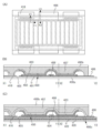


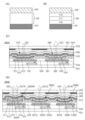


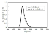


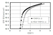


Classifications
-
- H—ELECTRICITY
- H10—SEMICONDUCTOR DEVICES; ELECTRIC SOLID-STATE DEVICES NOT OTHERWISE PROVIDED FOR
- H10K—ORGANIC ELECTRIC SOLID-STATE DEVICES
- H10K50/00—Organic light-emitting devices
- H10K50/10—OLEDs or polymer light-emitting diodes [PLED]
- H10K50/14—Carrier transporting layers
- H10K50/15—Hole transporting layers
- H10K50/156—Hole transporting layers comprising a multilayered structure
-
- H—ELECTRICITY
- H10—SEMICONDUCTOR DEVICES; ELECTRIC SOLID-STATE DEVICES NOT OTHERWISE PROVIDED FOR
- H10K—ORGANIC ELECTRIC SOLID-STATE DEVICES
- H10K85/00—Organic materials used in the body or electrodes of devices covered by this subclass
- H10K85/60—Organic compounds having low molecular weight
- H10K85/631—Amine compounds having at least two aryl rest on at least one amine-nitrogen atom, e.g. triphenylamine
- H10K85/633—Amine compounds having at least two aryl rest on at least one amine-nitrogen atom, e.g. triphenylamine comprising polycyclic condensed aromatic hydrocarbons as substituents on the nitrogen atom
-
- F—MECHANICAL ENGINEERING; LIGHTING; HEATING; WEAPONS; BLASTING
- F21—LIGHTING
- F21V—FUNCTIONAL FEATURES OR DETAILS OF LIGHTING DEVICES OR SYSTEMS THEREOF; STRUCTURAL COMBINATIONS OF LIGHTING DEVICES WITH OTHER ARTICLES, NOT OTHERWISE PROVIDED FOR
- F21V33/00—Structural combinations of lighting devices with other articles, not otherwise provided for
-
- G—PHYSICS
- G09—EDUCATION; CRYPTOGRAPHY; DISPLAY; ADVERTISING; SEALS
- G09F—DISPLAYING; ADVERTISING; SIGNS; LABELS OR NAME-PLATES; SEALS
- G09F9/00—Indicating arrangements for variable information in which the information is built-up on a support by selection or combination of individual elements
- G09F9/30—Indicating arrangements for variable information in which the information is built-up on a support by selection or combination of individual elements in which the desired character or characters are formed by combining individual elements
- G09F9/33—Indicating arrangements for variable information in which the information is built-up on a support by selection or combination of individual elements in which the desired character or characters are formed by combining individual elements being semiconductor devices, e.g. diodes
- G09F9/335—Indicating arrangements for variable information in which the information is built-up on a support by selection or combination of individual elements in which the desired character or characters are formed by combining individual elements being semiconductor devices, e.g. diodes being organic light emitting diodes [OLED]
-
- H—ELECTRICITY
- H05—ELECTRIC TECHNIQUES NOT OTHERWISE PROVIDED FOR
- H05B—ELECTRIC HEATING; ELECTRIC LIGHT SOURCES NOT OTHERWISE PROVIDED FOR; CIRCUIT ARRANGEMENTS FOR ELECTRIC LIGHT SOURCES, IN GENERAL
- H05B33/00—Electroluminescent light sources
- H05B33/12—Light sources with substantially two-dimensional radiating surfaces
- H05B33/20—Light sources with substantially two-dimensional radiating surfaces characterised by the chemical or physical composition or the arrangement of the material in which the electroluminescent material is embedded
-
- H—ELECTRICITY
- H10—SEMICONDUCTOR DEVICES; ELECTRIC SOLID-STATE DEVICES NOT OTHERWISE PROVIDED FOR
- H10K—ORGANIC ELECTRIC SOLID-STATE DEVICES
- H10K50/00—Organic light-emitting devices
- H10K50/10—OLEDs or polymer light-emitting diodes [PLED]
- H10K50/14—Carrier transporting layers
- H10K50/15—Hole transporting layers
-
- H—ELECTRICITY
- H10—SEMICONDUCTOR DEVICES; ELECTRIC SOLID-STATE DEVICES NOT OTHERWISE PROVIDED FOR
- H10K—ORGANIC ELECTRIC SOLID-STATE DEVICES
- H10K50/00—Organic light-emitting devices
- H10K50/80—Constructional details
- H10K50/805—Electrodes
- H10K50/81—Anodes
-
- H—ELECTRICITY
- H10—SEMICONDUCTOR DEVICES; ELECTRIC SOLID-STATE DEVICES NOT OTHERWISE PROVIDED FOR
- H10K—ORGANIC ELECTRIC SOLID-STATE DEVICES
- H10K50/00—Organic light-emitting devices
- H10K50/80—Constructional details
- H10K50/805—Electrodes
- H10K50/82—Cathodes
-
- H—ELECTRICITY
- H10—SEMICONDUCTOR DEVICES; ELECTRIC SOLID-STATE DEVICES NOT OTHERWISE PROVIDED FOR
- H10K—ORGANIC ELECTRIC SOLID-STATE DEVICES
- H10K50/00—Organic light-emitting devices
- H10K50/80—Constructional details
- H10K50/85—Arrangements for extracting light from the devices
- H10K50/858—Arrangements for extracting light from the devices comprising refractive means, e.g. lenses
-
- H—ELECTRICITY
- H10—SEMICONDUCTOR DEVICES; ELECTRIC SOLID-STATE DEVICES NOT OTHERWISE PROVIDED FOR
- H10K—ORGANIC ELECTRIC SOLID-STATE DEVICES
- H10K50/00—Organic light-emitting devices
- H10K50/80—Constructional details
- H10K50/88—Terminals, e.g. bond pads
-
- H—ELECTRICITY
- H10—SEMICONDUCTOR DEVICES; ELECTRIC SOLID-STATE DEVICES NOT OTHERWISE PROVIDED FOR
- H10K—ORGANIC ELECTRIC SOLID-STATE DEVICES
- H10K85/00—Organic materials used in the body or electrodes of devices covered by this subclass
- H10K85/30—Coordination compounds
- H10K85/341—Transition metal complexes, e.g. Ru(II)polypyridine complexes
- H10K85/342—Transition metal complexes, e.g. Ru(II)polypyridine complexes comprising iridium
-
- H—ELECTRICITY
- H10—SEMICONDUCTOR DEVICES; ELECTRIC SOLID-STATE DEVICES NOT OTHERWISE PROVIDED FOR
- H10K—ORGANIC ELECTRIC SOLID-STATE DEVICES
- H10K85/00—Organic materials used in the body or electrodes of devices covered by this subclass
- H10K85/60—Organic compounds having low molecular weight
- H10K85/631—Amine compounds having at least two aryl rest on at least one amine-nitrogen atom, e.g. triphenylamine
- H10K85/636—Amine compounds having at least two aryl rest on at least one amine-nitrogen atom, e.g. triphenylamine comprising heteroaromatic hydrocarbons as substituents on the nitrogen atom
-
- H—ELECTRICITY
- H10—SEMICONDUCTOR DEVICES; ELECTRIC SOLID-STATE DEVICES NOT OTHERWISE PROVIDED FOR
- H10K—ORGANIC ELECTRIC SOLID-STATE DEVICES
- H10K85/00—Organic materials used in the body or electrodes of devices covered by this subclass
- H10K85/60—Organic compounds having low molecular weight
- H10K85/649—Aromatic compounds comprising a hetero atom
- H10K85/654—Aromatic compounds comprising a hetero atom comprising only nitrogen as heteroatom
-
- H—ELECTRICITY
- H10—SEMICONDUCTOR DEVICES; ELECTRIC SOLID-STATE DEVICES NOT OTHERWISE PROVIDED FOR
- H10K—ORGANIC ELECTRIC SOLID-STATE DEVICES
- H10K85/00—Organic materials used in the body or electrodes of devices covered by this subclass
- H10K85/60—Organic compounds having low molecular weight
- H10K85/649—Aromatic compounds comprising a hetero atom
- H10K85/657—Polycyclic condensed heteroaromatic hydrocarbons
- H10K85/6572—Polycyclic condensed heteroaromatic hydrocarbons comprising only nitrogen in the heteroaromatic polycondensed ring system, e.g. phenanthroline or carbazole
-
- H—ELECTRICITY
- H10—SEMICONDUCTOR DEVICES; ELECTRIC SOLID-STATE DEVICES NOT OTHERWISE PROVIDED FOR
- H10K—ORGANIC ELECTRIC SOLID-STATE DEVICES
- H10K85/00—Organic materials used in the body or electrodes of devices covered by this subclass
- H10K85/60—Organic compounds having low molecular weight
- H10K85/649—Aromatic compounds comprising a hetero atom
- H10K85/657—Polycyclic condensed heteroaromatic hydrocarbons
- H10K85/6576—Polycyclic condensed heteroaromatic hydrocarbons comprising only sulfur in the heteroaromatic polycondensed ring system, e.g. benzothiophene
-
- F—MECHANICAL ENGINEERING; LIGHTING; HEATING; WEAPONS; BLASTING
- F21—LIGHTING
- F21Y—INDEXING SCHEME ASSOCIATED WITH SUBCLASSES F21K, F21L, F21S and F21V, RELATING TO THE FORM OR THE KIND OF THE LIGHT SOURCES OR OF THE COLOUR OF THE LIGHT EMITTED
- F21Y2115/00—Light-generating elements of semiconductor light sources
- F21Y2115/10—Light-emitting diodes [LED]
-
- H—ELECTRICITY
- H10—SEMICONDUCTOR DEVICES; ELECTRIC SOLID-STATE DEVICES NOT OTHERWISE PROVIDED FOR
- H10K—ORGANIC ELECTRIC SOLID-STATE DEVICES
- H10K2101/00—Properties of the organic materials covered by group H10K85/00
- H10K2101/30—Highest occupied molecular orbital [HOMO], lowest unoccupied molecular orbital [LUMO] or Fermi energy values
-
- H—ELECTRICITY
- H10—SEMICONDUCTOR DEVICES; ELECTRIC SOLID-STATE DEVICES NOT OTHERWISE PROVIDED FOR
- H10K—ORGANIC ELECTRIC SOLID-STATE DEVICES
- H10K2101/00—Properties of the organic materials covered by group H10K85/00
- H10K2101/40—Interrelation of parameters between multiple constituent active layers or sublayers, e.g. HOMO values in adjacent layers
Abstract
발광 효율이 높은 발광 디바이스를 제공한다. 구동 전압이 낮은 발광 디바이스를 제공한다. 제 1 전극과, 제 1 전극 위의 제 1 층과, 제 1 층 위의 제 2 층과, 제 2 층 위의 발광층과, 발광층 위의 제 2 전극을 가지는 발광 디바이스이다. 제 1 층은 제 1 유기 화합물을 가지고, 제 2 층은 제 2 유기 화합물을 가진다. 제 1 유기 화합물에 있어서 sp3 혼성 궤도에서 결합을 형성하는 탄소수의 총 탄소수에 대한 비율은 23퍼센트 이상 55퍼센트 이하이다. 제 2 유기 화합물은 플루오린을 포함한다.A light emitting device with high luminous efficiency is provided. A light emitting device with a low driving voltage is provided. A light emitting device having a first electrode, a first layer over the first electrode, a second layer over the first layer, a light emitting layer over the second layer, and a second electrode over the light emitting layer. The first layer has a first organic compound and the second layer has a second organic compound. In the first organic compound, the ratio of the number of carbon atoms forming bonds in the sp3 hybrid orbital to the total number of carbon atoms is 23% or more and 55% or less. The second organic compound includes fluorine.
Description
본 발명의 일 형태는 발광 디바이스, 수광 디바이스, 및 수발광 디바이스 등의 광 디바이스에 관한 것이다. 본 발명의 일 형태는 발광 장치, 수광 장치, 및 수발광 장치 등의 장치에 관한 것이다. 본 발명의 일 형태는 발광 모듈, 수광 모듈, 수발광 모듈, 표시 모듈, 및 조명 모듈 등의 모듈에 관한 것이다. 본 발명의 일 형태는 전자 기기, 및 조명 장치에 관한 것이다.One embodiment of the present invention relates to an optical device such as a light emitting device, a light receiving device, and a light receiving device. One embodiment of the present invention relates to devices such as a light emitting device, a light receiving device, and a light receiving device. One embodiment of the present invention relates to modules such as a light emitting module, a light receiving module, a light receiving module, a display module, and a lighting module. One embodiment of the present invention relates to an electronic device and a lighting device.
또한 본 발명의 일 형태는 상기 기술분야에 한정되지 않는다. 본 발명의 일 형태의 기술분야로서는, 반도체 장치, 표시 장치, 발광 장치, 축전 장치, 기억 장치, 전자 기기, 조명 장치, 입력 장치(예를 들어, 터치 센서), 입출력 장치(예를 들어, 터치 패널), 이들의 구동 방법, 또는 이들의 제조 방법을 일례로서 들 수 있다.Also, one embodiment of the present invention is not limited to the above technical fields. As the technical field of one embodiment of the present invention, a semiconductor device, a display device, a light emitting device, a power storage device, a memory device, an electronic device, a lighting device, an input device (eg, a touch sensor), an input/output device (eg, a touch sensor) panels), their driving methods, or their manufacturing methods are exemplified.
유기 일렉트로루미네선스(EL: Electro Luminescence) 현상을 이용한 발광 디바이스(유기 EL 디바이스, 유기 EL 소자라고도 함)의 연구 개발이 활발히 이루어지고 있다. 유기 EL 디바이스의 기본적인 구성은 한 쌍의 전극 사이에 발광성 유기 화합물을 포함한 층(이후, 발광층이라고도 기재함)을 끼운 것이다. 이 유기 EL 디바이스에 전압을 인가함으로써, 발광성 유기 화합물로부터의 발광을 얻을 수 있다.BACKGROUND ART Research and development of a light emitting device (also referred to as an organic EL device or an organic EL device) using an organic electroluminescence (EL) phenomenon is being actively conducted. The basic configuration of an organic EL device is to sandwich a layer containing a light emitting organic compound (hereinafter also referred to as a light emitting layer) between a pair of electrodes. By applying a voltage to this organic EL device, light emission from the light-emitting organic compound can be obtained.
유기 EL 디바이스는 박형 경량화가 용이하고, 입력 신호에 대한 고속 응답이 가능하고, 직류 정전압 전원을 사용한 구동이 가능하다는 등의 특징을 가지므로 표시 장치에 적합하다.Organic EL devices are suitable for display devices because they have characteristics such as easy thinness and light weight, high-speed response to input signals, and ability to be driven using a DC constant voltage power supply.
또한 유기 EL 디바이스는 막 형상으로 형성할 수 있기 때문에 면발광을 얻을 수 있다. 따라서, 대면적의 발광 디바이스를 용이하게 형성할 수 있다. 이는, LED(발광 다이오드)로 대표되는 점광원 및 형광등으로 대표되는 선광원으로는 얻기 어려운 특색이기 때문에 유기 EL 디바이스는 조명 장치 등에 응용할 수 있는 면광원으로서의 이용 가치도 높다.In addition, since the organic EL device can be formed in a film shape, surface light emission can be obtained. Therefore, it is possible to easily form a large-area light emitting device. Since this is a characteristic that is difficult to obtain with point light sources represented by LEDs (light emitting diodes) and linear light sources represented by fluorescent lamps, organic EL devices are also highly useful as surface light sources applicable to lighting devices and the like.
유기 EL 디바이스에 있어서, 광 추출 효율을 더욱 향상시키는 것이 요구되고 있다. 서로 인접한 층의 굴절률의 차이로 일어나는 반사로 인한 광의 감쇠는 광 추출 효율을 저하시키는 요인의 하나이다. 유기 EL 디바이스에 있어서, 굴절률이 낮은 재료를 사용함으로써, 광 추출 효율을 향상시킬 수 있다. 예를 들어, 비특허문헌 1에서는, 굴절률이 낮은 층을 가지는 유기 EL 디바이스가 개시(開示)되어 있다.[0003] In organic EL devices, it is desired to further improve the light extraction efficiency. Attenuation of light due to reflection caused by a difference in refractive index of adjacent layers is one of the factors that lower light extraction efficiency. In the organic EL device, the light extraction efficiency can be improved by using a material having a low refractive index. For example, in Non-Patent
한편, 유기 EL 디바이스에 사용하는 재료에 있어서, 낮은 굴절률과 높은 신뢰성 또는 높은 내열성을 양립하기는 어렵다.On the other hand, in materials used for organic EL devices, it is difficult to achieve both low refractive index and high reliability or high heat resistance.
본 발명의 일 형태는 발광 효율이 높은 발광 디바이스 또는 수발광 디바이스를 제공하는 것을 과제의 하나로 한다. 본 발명의 일 형태는 광 추출 효율이 높은 발광 디바이스 또는 수발광 디바이스를 제공하는 것을 과제의 하나로 한다. 본 발명의 일 형태는 구동 전압이 낮은 발광 디바이스, 수광 디바이스, 또는 수발광 디바이스를 제공하는 것을 과제의 하나로 한다. 본 발명의 일 형태는 내열성이 높은 발광 디바이스, 수광 디바이스, 또는 수발광 디바이스를 제공하는 것을 과제의 하나로 한다. 본 발명의 일 형태는 장수명의 발광 디바이스, 수광 디바이스, 또는 수발광 디바이스를 제공하는 것을 과제의 하나로 한다. 본 발명의 일 형태는 소비 전력이 낮은 발광 디바이스, 수광 디바이스, 또는 수발광 디바이스를 제공하는 것을 과제의 하나로 한다.An object of one embodiment of the present invention is to provide a light-emitting device or a light-receiving device having high luminous efficiency. An object of one embodiment of the present invention is to provide a light-emitting device or a light-receiving device having high light extraction efficiency. An object of one embodiment of the present invention is to provide a light emitting device, a light receiving device, or a light receiving device having a low driving voltage. An object of one embodiment of the present invention is to provide a light-emitting device, a light-receiving device, or a light-receiving device having high heat resistance. An object of one embodiment of the present invention is to provide a long-life light-emitting device, light-receiving device, or light-receiving device. An object of one embodiment of the present invention is to provide a light-emitting device, a light-receiving device, or a light-receiving device with low power consumption.
또한 이들 과제의 기재는 다른 과제의 존재를 방해하는 것은 아니다. 본 발명의 일 형태는 이들 과제 모두를 반드시 해결할 필요는 없는 것으로 한다. 명세서, 도면, 청구항의 기재로부터 이들 외의 과제를 추출할 수 있다.In addition, the description of these subjects does not obstruct the existence of other subjects. In one embodiment of the present invention, it is not necessary to necessarily solve all of these problems. Subjects other than these can be extracted from the description of the specification, drawings, and claims.
본 발명의 일 형태는 제 1 전극과, 제 1 전극 위의 제 1 층과, 제 1 층 위의 제 2 층과, 제 2 층 위의 발광층과, 발광층 위의 제 2 전극을 가지고, 제 1 층은 제 1 유기 화합물을 가지고, 제 2 층은 제 2 유기 화합물을 가지고, 제 1 유기 화합물에 있어서 sp3 혼성 궤도에서 결합을 형성하는 탄소수의 총 탄소수에 대한 비율은 23% 이상 55% 이하이고, 제 2 유기 화합물은 플루오린을 포함하는 발광 디바이스이다. 제 1 유기 화합물로 이루어지는 층의 파장 633nm의 광에서의 굴절률은 1.45 이상 1.70 이하인 것이 바람직하다.One aspect of the present invention includes a first electrode, a first layer on the first electrode, a second layer on the first layer, a light emitting layer on the second layer, and a second electrode on the light emitting layer, The layer has a first organic compound, the second layer has a second organic compound, and in the first organic compound, the ratio of the number of carbon atoms forming bonds in the sp3 hybrid orbital to the total number of carbon atoms is 23% or more and 55% or less, The second organic compound is a light emitting device containing fluorine. The refractive index of the layer made of the first organic compound in light having a wavelength of 633 nm is preferably 1.45 or more and 1.70 or less.
또는, 본 발명의 일 형태는 제 1 전극과, 제 1 전극 위의 제 1 층과, 제 1 층 위의 제 2 층과, 제 2 층 위의 발광층과, 발광층 위의 제 2 전극을 가지고, 제 1 층은 제 1 유기 화합물을 가지고, 제 2 층은 제 2 유기 화합물을 가지고, 제 1 유기 화합물의 유리 전이 온도는 90℃ 이상이고, 제 1 유기 화합물로 이루어지는 층의 파장 633nm의 광에서의 굴절률은 1.45 이상 1.70 이하이고, 제 2 유기 화합물은 플루오린을 포함하는 발광 디바이스이다.Alternatively, one embodiment of the present invention has a first electrode, a first layer on the first electrode, a second layer on the first layer, a light emitting layer on the second layer, and a second electrode on the light emitting layer, The first layer has a first organic compound, the second layer has a second organic compound, the glass transition temperature of the first organic compound is 90° C. or higher, and the layer made of the first organic compound has a wavelength of 633 nm in light. The refractive index is 1.45 or more and 1.70 or less, and the second organic compound is a light emitting device containing fluorine.
제 1 유기 화합물은 아민 화합물인 것이 바람직하고, 모노아민 화합물인 것이 더 바람직하다.The first organic compound is preferably an amine compound, more preferably a monoamine compound.
또는, 본 발명의 일 형태는 제 1 전극과, 제 1 전극 위의 제 1 층과, 제 1 층 위의 제 2 층과, 제 2 층 위의 발광층과, 발광층 위의 제 2 전극을 가지고, 제 1 층은 제 1 유기 화합물을 가지고, 제 2 층은 제 2 유기 화합물을 가지고, 제 1 유기 화합물은 모노아민 화합물이고, 제 1 유기 화합물로 이루어지는 층의 파장 633nm의 광에서의 굴절률은 1.45 이상 1.70 이하이고, 제 2 유기 화합물은 플루오린을 포함하는 발광 디바이스이다.Alternatively, one embodiment of the present invention has a first electrode, a first layer on the first electrode, a second layer on the first layer, a light emitting layer on the second layer, and a second electrode on the light emitting layer, The first layer has a first organic compound, the second layer has a second organic compound, the first organic compound is a monoamine compound, and the layer made of the first organic compound has a refractive index of 1.45 or more in light with a wavelength of 633 nm. 1.70 or less, and the second organic compound is a light emitting device containing fluorine.
제 2 층은 제 3 유기 화합물을 더 가져도 좋다. 제 3 유기 화합물의 최고 점유 분자 궤도(HOMO) 준위는 제 1 유기 화합물의 HOMO 준위보다 낮은 것이 바람직하다.The second layer may further have a third organic compound. Preferably, the highest occupied molecular orbital (HOMO) level of the third organic compound is lower than that of the first organic compound.
상술한 어느 구성의 발광 디바이스는 제 3 층을 더 가져도 좋다. 제 3 층은 제 2 층과 발광층 사이에 위치한다. 제 3 층은 제 3 유기 화합물을 가진다. 제 3 유기 화합물의 HOMO 준위는 제 1 유기 화합물의 HOMO 준위보다 낮다. 이 경우에도 제 2 층은 제 3 유기 화합물을 더 가져도 좋다.A light emitting device having any of the structures described above may further include a third layer. The third layer is positioned between the second layer and the light emitting layer. The third layer has a third organic compound. The HOMO level of the third organic compound is lower than that of the first organic compound. Also in this case, the second layer may further have a third organic compound.
또는, 본 발명의 일 형태는 제 1 전극과, 제 1 전극 위의 제 1 층과, 제 1 층 위의 제 2 층과, 제 2 층 위의 제 3 층과, 제 3 층 위의 발광층과, 발광층 위의 제 2 전극을 가지고, 제 1 층은 제 1 유기 화합물을 가지고, 제 2 층은 제 2 유기 화합물을 가지고, 제 3 층은 제 3 유기 화합물을 가지고, 제 3 유기 화합물의 HOMO 준위는 제 1 유기 화합물의 HOMO 준위보다 낮고, 제 1 유기 화합물로 이루어지는 층의 굴절률은 제 3 유기 화합물로 이루어지는 층의 굴절률보다 낮고, 제 2 유기 화합물은 플루오린을 포함하는 발광 디바이스이다.Alternatively, one embodiment of the present invention is a first electrode, a first layer over the first electrode, a second layer over the first layer, a third layer over the second layer, and a light emitting layer over the third layer. , with a second electrode on the light emitting layer, the first layer has a first organic compound, the second layer has a second organic compound, and the third layer has a third organic compound, the HOMO level of the third organic compound is lower than the HOMO level of the first organic compound, the refractive index of the layer made of the first organic compound is lower than the refractive index of the layer made of the third organic compound, and the second organic compound is a light emitting device containing fluorine.
제 1 유기 화합물로 이루어지는 층의 파장 633nm의 광에서의 굴절률과 제 3 유기 화합물로 이루어지는 층의 파장 633nm의 광에서의 굴절률의 차이는 0.05 이상인 것이 바람직하고, 0.1 이상인 것이 더 바람직하다.The difference between the refractive index of the layer made of the first organic compound in light with a wavelength of 633 nm and the refractive index of the layer made of the third organic compound in light with a wavelength of 633 nm is preferably 0.05 or more, more preferably 0.1 or more.
제 2 층은 제 3 유기 화합물을 더 가져도 좋다. 제 3 층은 제 2 유기 화합물을 더 가져도 좋다.The second layer may further have a third organic compound. The 3rd layer may further have a 2nd organic compound.
제 1 유기 화합물로 이루어지는 층의 파장 633nm의 광에서의 굴절률은 1.45 이상 1.70 이하인 것이 바람직하다.The refractive index of the layer made of the first organic compound in light having a wavelength of 633 nm is preferably 1.45 or more and 1.70 or less.
제 1 유기 화합물의 유리 전이 온도는 90℃ 이상인 것이 바람직하다.It is preferable that the glass transition temperature of the 1st organic compound is 90 degreeC or more.
제 1 유기 화합물은 아민 화합물인 것이 바람직하고, 모노아민 화합물인 것이 더 바람직하다.The first organic compound is preferably an amine compound, more preferably a monoamine compound.
제 2 유기 화합물은 제 3 유기 화합물에 대하여 전자 수용성을 나타내는 것이 바람직하다.It is preferable that the second organic compound exhibits electron-accepting property with respect to the third organic compound.
제 3 유기 화합물에 있어서 sp3 혼성 궤도에서 결합을 형성하는 탄소수의 총 탄소수에 대한 비율은 23% 이상 55% 이하인 것이 바람직하다.In the third organic compound, the ratio of the number of carbon atoms forming bonds in the sp3 hybrid orbital to the total number of carbon atoms is preferably 23% or more and 55% or less.
제 3 유기 화합물로 이루어지는 층의 파장 633nm의 광에서의 굴절률은 1.45 이상 1.70 이하인 것이 바람직하다.It is preferable that the refractive index of the layer made of the third organic compound in light with a wavelength of 633 nm is 1.45 or more and 1.70 or less.
제 3 유기 화합물의 유리 전이 온도는 90℃ 이상인 것이 바람직하다.It is preferable that the glass transition temperature of the 3rd organic compound is 90 degreeC or more.
제 1 층은 제 2 층과 접하는 것이 바람직하다.The first layer is preferably in contact with the second layer.
상술한 어느 구성의 발광 디바이스는 제 4 층을 더 가져도 좋다. 제 4 층은 제 1 전극과 제 1 층 사이에 위치한다. 제 4 층은 제 1 유기 화합물과 제 2 유기 화합물을 가진다. 제 4 층은 제 1 전극과 접하는 것이 바람직하다. 제 4 층은 제 1 층과 접하는 것이 바람직하다.A light emitting device having any of the structures described above may further include a fourth layer. The fourth layer is located between the first electrode and the first layer. The fourth layer has a first organic compound and a second organic compound. The fourth layer is preferably in contact with the first electrode. The fourth layer is preferably in contact with the first layer.
제 1 유기 화합물의 분자량은 650 이상 1200 이하인 것이 바람직하다.It is preferable that the molecular weight of the 1st organic compound is 650 or more and 1200 or less.
제 1 유기 화합물은 트라이아릴모노아민 화합물인 것이 바람직하다.The first organic compound is preferably a triarylmonoamine compound.
제 1 유기 화합물의 1H-NMR 측정 결과에서의 4ppm 미만의 시그널의 적분값은 4ppm 이상의 시그널의 적분값보다 큰 것이 바람직하다.It is preferable that the integral of the signal of less than 4 ppm in the 1 H-NMR measurement result of the first organic compound is larger than the integral of the signal of 4 ppm or more.
제 1 유기 화합물은 탄소수 1 이상 12 이하의 탄화수소기를 적어도 하나 가지는 것이 바람직하다.It is preferable that the 1st organic compound has at least one hydrocarbon group of 1 or more and 12 or less carbon atoms.
제 1 유기 화합물은 탄소수 3 이상 8 이하의 알킬기 및 탄소수 6 이상 12 이하의 사이클로알킬기 중 적어도 한쪽을 가지는 것이 바람직하다.The first organic compound preferably has at least one of an alkyl group having 3 to 8 carbon atoms and a cycloalkyl group having 6 to 12 carbon atoms.
제 2 유기 화합물은 사이아노기를 포함하는 것이 바람직하다.It is preferable that the 2nd organic compound contains a cyano group.
제 2 유기 화합물의 최저 비점유 분자 궤도(LUMO) 준위는 -5.0eV 이하인 것이 바람직하다.The lowest unoccupied molecular orbital (LUMO) level of the second organic compound is preferably -5.0 eV or less.
제 2 유기 화합물은 제 1 유기 화합물에 대하여 전자 수용성을 나타내는 것이 바람직하다.The second organic compound is preferably electron accepting with respect to the first organic compound.
제 2 유기 화합물은 금속 원소를 포함하지 않는 것이 바람직하다.It is preferable that the second organic compound does not contain a metal element.
본 발명의 일 형태는 상술한 어느 구성의 발광 디바이스와, 트랜지스터 및 기판 중 적어도 한쪽을 가지는 장치이다.One embodiment of the present invention is an apparatus including a light emitting device having any of the above configurations, and at least one of a transistor and a substrate.
본 발명의 일 형태는 상기 발광 장치와, 커넥터 및 집적 회로(IC) 중 적어도 한쪽을 가지는 발광 모듈이다. 커넥터로서는 플렉시블 프린트 회로 기판(Flexible Printed Circuit, 이하, FPC라고도 기재함) 및 TCP(Tape Carrier Package) 등을 들 수 있다. IC는 COG(Chip On Glass) 방식 또는 COF(Chip On Film) 방식 등에 의하여 장치에 실장할 수 있다. 또한 본 발명의 일 형태의 발광 모듈은 커넥터 및 IC 중 한쪽만을 가져도 좋고 양쪽을 가져도 좋다.One embodiment of the present invention is a light emitting module having at least one of the light emitting device, a connector, and an integrated circuit (IC). As a connector, a flexible printed circuit board (Flexible Printed Circuit, hereinafter also described as FPC), TCP (Tape Carrier Package), etc. are mentioned. The IC may be mounted on a device by a COG (Chip On Glass) method or a COF (Chip On Film) method. In addition, the light emitting module of one embodiment of the present invention may have only one of a connector and an IC, or may have both.
본 발명의 일 형태는 상기 발광 장치와, 안테나, 배터리, 하우징, 카메라, 스피커, 마이크로폰, 및 조작 버튼 중 적어도 하나를 가지는 전자 기기이다.One embodiment of the present invention is an electronic device having at least one of the light emitting device, an antenna, a battery, a housing, a camera, a speaker, a microphone, and an operation button.
본 발명의 일 형태는 상술한 어느 구성을 가지는 발광 디바이스와, 하우징, 커버, 및 지지대 중 적어도 하나를 가지는 조명 장치이다.One aspect of the present invention is a lighting device having a light emitting device having any of the above configurations, and at least one of a housing, a cover, and a support.
본 발명의 일 형태에 따르면 발광 효율이 높은 발광 디바이스 또는 수발광 디바이스를 제공할 수 있다. 본 발명의 일 형태에 따르면 광 추출 효율이 높은 발광 디바이스 또는 수발광 디바이스를 제공할 수 있다. 본 발명의 일 형태에 따르면 구동 전압이 낮은 발광 디바이스, 수광 디바이스, 또는 수발광 디바이스를 제공할 수 있다. 본 발명의 일 형태에 따르면 내열성이 높은 발광 디바이스, 수광 디바이스, 또는 수발광 디바이스를 제공할 수 있다. 본 발명의 일 형태에 따르면 장수명의 발광 디바이스, 수광 디바이스, 또는 수발광 디바이스를 제공할 수 있다. 본 발명의 일 형태에 따르면 소비 전력이 낮은 발광 디바이스, 수광 디바이스, 또는 수발광 디바이스를 제공할 수 있다.According to one aspect of the present invention, a light emitting device or a light emitting device having high light emitting efficiency can be provided. According to one embodiment of the present invention, a light emitting device or a light emitting device having high light extraction efficiency can be provided. According to one embodiment of the present invention, a light emitting device, a light receiving device, or a light receiving device having a low drive voltage can be provided. According to one embodiment of the present invention, a light emitting device, a light receiving device, or a light receiving device having high heat resistance can be provided. According to one embodiment of the present invention, a light emitting device, a light receiving device, or a light receiving device having a long lifespan can be provided. According to one embodiment of the present invention, a light emitting device, a light receiving device, or a light receiving device with low power consumption can be provided.
또한, 이들 효과의 기재는 다른 효과의 존재를 방해하는 것이 아니다. 본 발명의 일 형태는 반드시 이들 효과 모두를 가질 필요는 없다. 명세서, 도면, 청구항의 기재로부터 이들 외의 효과를 추출할 수 있다.Also, the description of these effects does not preclude the existence of other effects. One embodiment of the present invention does not necessarily have all of these effects. Effects other than these can be extracted from the description of the specification, drawings, and claims.
도 1의 (A) 내지 (E)는 발광 디바이스의 일례를 나타낸 단면도이다.
도 2의 (A)는 발광 장치의 일례를 나타낸 상면도이다. 도 2의 (B), (C)는 발광 장치의 일례를 나타낸 단면도이다.
도 3의 (A), (C)는 발광 장치의 일례를 나타낸 단면도이다. 도 3의 (B)는 발광 디바이스의 일례를 나타낸 단면도이다.
도 4의 (A), (B)는 발광 장치의 일례를 나타낸 단면도이다.
도 5의 (A)는 발광 장치의 일례를 나타낸 단면도이다. 도 5의 (B)는 발광 장치의 일례를 나타낸 단면도이다. 도 5의 (C), (D)는 트랜지스터의 일례를 나타낸 단면도이다.
도 6의 (A), (B)는 수광 디바이스의 일례를 나타낸 단면도이다. 도 6의 (C), (D)는 수발광 장치의 일례를 나타낸 도면이다.
도 7의 (A) 내지 (C)는 표시 장치의 일례를 나타낸 도면이다.
도 8의 (A) 내지 (D)는 전자 기기의 일례를 나타낸 도면이다.
도 9의 (A) 내지 (F)는 전자 기기의 일례를 나타낸 도면이다.
도 10의 (A) 내지 (C)는 자동차의 일례를 나타낸 도면이다.
도 11의 (A) 내지 (E)는 전자 기기의 일례를 나타낸 도면이다.
도 12는 실시예의 발광 디바이스를 나타낸 단면도이다.
도 13은 dchPAF 및 PCBBiF의 굴절률의 측정 결과를 나타낸 도면이다.
도 14는 실시예 1의 발광 디바이스의 휘도-전류 밀도 특성을 나타낸 도면이다.
도 15는 실시예 1의 발광 디바이스의 전류 효율-휘도 특성을 나타낸 도면이다.
도 16은 실시예 1의 발광 디바이스의 전류 밀도-전압 특성을 나타낸 도면이다.
도 17은 실시예 1의 발광 디바이스의 외부 양자 효율-휘도 특성을 나타낸 도면이다.
도 18은 실시예 1의 발광 디바이스의 발광 스펙트럼을 나타낸 도면이다.
도 19는 실시예 1의 발광 디바이스의 신뢰성 시험의 결과를 나타낸 도면이다.
도 20은 mmtBumTPoFBi-04의 굴절률의 측정 결과를 나타낸 도면이다.
도 21은 실시예 2의 발광 디바이스의 휘도-전류 밀도 특성을 나타낸 도면이다.
도 22는 실시예 2의 발광 디바이스의 전류 효율-휘도 특성을 나타낸 도면이다.
도 23은 실시예 2의 발광 디바이스의 전류 밀도-전압 특성을 나타낸 도면이다.
도 24는 실시예 2의 발광 디바이스의 외부 양자 효율-휘도 특성을 나타낸 도면이다.
도 25는 실시예 2의 발광 디바이스의 발광 스펙트럼을 나타낸 도면이다.1(A) to (E) are cross-sectional views showing an example of a light emitting device.
2(A) is a top view showing an example of the light emitting device. 2(B) and (C) are cross-sectional views showing an example of the light emitting device.
3(A) and (C) are cross-sectional views showing an example of the light emitting device. 3(B) is a cross-sectional view showing an example of a light emitting device.
4(A) and (B) are cross-sectional views showing an example of the light emitting device.
5(A) is a cross-sectional view showing an example of a light emitting device. 5(B) is a cross-sectional view showing an example of the light emitting device. 5(C) and (D) are cross-sectional views showing an example of a transistor.
6(A) and (B) are sectional views showing an example of the light receiving device. 6(C) and (D) are views showing an example of a light receiving and emitting device.
7(A) to (C) are diagrams showing an example of a display device.
8(A) to (D) are views showing an example of an electronic device.
9(A) to (F) are views showing an example of an electronic device.
10(A) to (C) are diagrams showing an example of a vehicle.
11(A) to (E) are views showing an example of an electronic device.
12 is a cross-sectional view showing a light emitting device of an embodiment.
13 is a diagram showing measurement results of refractive indices of dchPAF and PCBBiF.
14 is a diagram showing luminance-current density characteristics of the light emitting device of Example 1;
15 is a diagram showing current efficiency-luminance characteristics of the light emitting device of Example 1;
16 is a diagram showing current density-voltage characteristics of the light emitting device of Example 1;
17 is a diagram showing external quantum efficiency-luminance characteristics of the light emitting device of Example 1;
18 is a diagram showing the emission spectrum of the light emitting device of Example 1;
Fig. 19 is a diagram showing the results of a reliability test of the light emitting device of Example 1;
20 is a diagram showing measurement results of the refractive index of mmtBumTPoFBi-04.
21 is a diagram showing luminance-current density characteristics of the light emitting device of Example 2;
22 is a diagram showing current efficiency-luminance characteristics of the light emitting device of Example 2;
23 is a diagram showing current density-voltage characteristics of the light emitting device of Example 2;
24 is a diagram showing external quantum efficiency-luminance characteristics of the light emitting device of Example 2;
25 is a diagram showing the emission spectrum of the light emitting device of Example 2;
실시형태에 대해서 도면을 참조하여 자세히 설명한다. 다만 본 발명은 이하의 설명에 한정되지 않고, 본 발명의 취지 및 그 범위에서 벗어남이 없이 그 형태 및 자세한 사항을 다양하게 변경할 수 있다는 것은 통상의 기술자라면 용이하게 이해할 수 있다. 따라서 본 발명은 이하의 실시형태의 기재 내용에 한정하여 해석되는 것은 아니다.EMBODIMENT OF THE INVENTION Embodiment is demonstrated in detail with reference to drawings. However, the present invention is not limited to the following description, and it can be easily understood by those skilled in the art that the form and details can be variously changed without departing from the spirit and scope of the present invention. Therefore, the present invention is not construed as being limited to the description of the following embodiments.
또한 아래에서 설명되는 발명의 구성에서, 동일한 부분 또는 같은 기능을 가지는 부분에는 동일한 부호를 상이한 도면 사이에서 공통적으로 사용하고, 이에 대한 반복적인 설명은 생략한다. 또한 같은 기능을 가지는 부분을 가리키는 경우에는, 같은 해치 패턴으로 하고, 특별히 부호를 붙이지 않는 경우가 있다.In addition, in the configuration of the invention described below, the same reference numerals are commonly used in different drawings for the same parts or parts having the same functions, and repetitive description thereof will be omitted. In addition, when indicating parts having the same function, the same hatch pattern may be used and no special code is attached.
또한, 도면에서 나타내는 각 구성의 위치, 크기, 및 범위 등은 이해를 용이하게 하기 위하여 실제의 위치, 크기, 및 범위 등을 나타내지 않는 경우가 있다. 그러므로, 개시하는 발명은 반드시 도면에 개시된 위치, 크기, 및 범위 등에 한정되지 않는다.In addition, the position, size, range, etc. of each component shown in the drawings may not indicate the actual position, size, range, etc. for easy understanding. Therefore, the disclosed invention is not necessarily limited to the position, size, range, etc. disclosed in the drawings.
또한 '막'이라는 용어와 '층'이라는 용어는 경우에 따라 또는 상황에 따라 서로 바꿀 수 있다. 예를 들어 '도전층'이라는 용어를 '도전막'이라는 용어로 변경할 수 있다. 또는 예를 들어 '절연막'이라는 용어를 '절연층'이라는 용어로 변경할 수 있다.In addition, the terms 'film' and 'layer' may be interchanged depending on the case or circumstances. For example, the term 'conductive layer' may be changed to the term 'conductive layer'. Alternatively, for example, the term 'insulating layer' may be changed to the term 'insulating layer'.
(실시형태 1)(Embodiment 1)
본 실시형태에서는 본 발명의 일 형태의 발광 디바이스에 대하여 도 1을 참조하여 설명한다.In this embodiment, a light emitting device of one embodiment of the present invention will be described with reference to FIG. 1 .
유기 EL 디바이스는 사용하는 재료의 굴절률을 낮춤으로써, 외부 양자 효율을 높일 수 있다. 굴절률이 낮은 재료를 얻기 위해서는, 분자 내에 원자 굴절이 낮은 치환기를 도입하는 것이 바람직하다. 상기 치환기로서는 쇄식 포화 탄화수소기 및 환식 포화 탄화수소기 등을 들 수 있다. 그러나, 이들 치환기는 캐리어 수송성의 발현을 방해한다. 따라서, 높은 캐리어 수송성과 낮은 굴절률을 양립시키기는 어렵다고 할 수 있다.The organic EL device can increase external quantum efficiency by lowering the refractive index of the material used. In order to obtain a material having a low refractive index, it is preferable to introduce a substituent having a low atomic refraction into the molecule. Examples of the substituent include chain saturated hydrocarbon groups and cyclic saturated hydrocarbon groups. However, these substituents hinder expression of carrier transportability. Therefore, it can be said that it is difficult to achieve both high carrier transportability and low refractive index.
또한, 유기 EL 디바이스의 신뢰성을 높이기 위하여, 유기 EL 디바이스에 사용하는 재료의 유리 전이 온도(Tg)는 높은 것이 바람직하다. 유리 전이 온도를 높이기 위해서는, 재료의 분자량을 높이는 것이 요구된다. 내열성이 높고, 신뢰성이 양호한 재료를 얻기 위한 하나의 방법으로서, 불포화 탄화수소기, 특히 환식 불포화 탄화수소기를 분자 내에 도입하는 방법을 생각할 수 있다. 그러나, 분자량을 높이기 위하여 불포화 결합을 가지는 골격을 분자 내에 도입하면, 재료의 굴절률이 높아진다. 이와 같이, 높은 유리 전이 온도와 낮은 굴절률도 양립시키기 어렵다.Further, in order to increase the reliability of the organic EL device, it is preferable that the glass transition temperature (Tg) of the material used for the organic EL device is high. In order to raise the glass transition temperature, it is required to increase the molecular weight of the material. As one method for obtaining a material with high heat resistance and good reliability, a method of introducing an unsaturated hydrocarbon group, particularly a cyclic unsaturated hydrocarbon group, into a molecule can be considered. However, when a skeleton having an unsaturated bond is introduced into the molecule to increase the molecular weight, the refractive index of the material increases. Thus, it is difficult to achieve both a high glass transition temperature and a low refractive index.
유기 EL 디바이스에 사용할 수 있는 정공 수송성 재료 중에서도 굴절률이 낮은 재료의 하나로서 1,1-비스-(4-비스(4-메틸-페닐)-아미노-페닐)사이클로헥세인(약칭: TAPC)이 알려져 있다. TAPC를 사용함으로써, 양호한 외부 양자 효율을 가지는 발광 디바이스를 얻을 수 있는 것이 기대된다.1,1-bis-(4-bis(4-methyl-phenyl)-amino-phenyl)cyclohexane (abbreviation: TAPC) is known as one of the materials having a low refractive index among hole-transporting materials usable for organic EL devices. there is. By using TAPC, it is expected that a light emitting device having good external quantum efficiency can be obtained.
일반적으로, 높은 캐리어 수송성과 낮은 굴절률은 트레이드오프의 관계에 있다. 이는 유기 화합물에서의 캐리어 수송성은 불포화 결합의 존재에서 유래되는 바가 크고, 불포화 결합을 많이 가지는 유기 화합물은 굴절률이 높은 경향이 있기 때문이다. TAPC는 캐리어 수송성과 낮은 굴절률이 절묘한 균형을 이루는 물질이다. 한편, TAPC와 같이 사이클로헥세인의 1,1-다이치환 구조를 가지는 화합물은 사이클로헥세인의 하나의 탄소 위에, 부피가 큰 치환기가 2개 삽입되기 때문에 입체 반발이 커지므로 분자 자체가 불안정해지기 때문에, 신뢰성의 관점에서 불리하다. 또한, TAPC는 그 골격의 구성이 사이클로헥세인과 단순한 벤젠 고리로 이루어지기 때문에 유리 전이 온도가 85℃로 낮고, 내열성에도 문제를 가진다.In general, high carrier transport and low refractive index are in a trade-off relationship. This is because the carrier transportability of organic compounds is largely derived from the presence of unsaturated bonds, and organic compounds having many unsaturated bonds tend to have a high refractive index. TAPC is a material with an exquisite balance of carrier transport and low refractive index. On the other hand, compounds having a 1,1-disubstituted structure of cyclohexane, such as TAPC, become unstable because steric repulsion increases because two bulky substituents are inserted on one carbon of cyclohexane. Therefore, it is disadvantageous from a reliability point of view. In addition, TAPC has a glass transition temperature as low as 85 ° C. and has a problem in heat resistance because its skeleton is composed of cyclohexane and a simple benzene ring.
상술한 바와 같이, 정공 수송성 재료에 있어서, 높은 캐리어 수송성과, 낮은 굴절률을 겸비하면서, 유리 전이 온도를 더 향상시켜 내열성을 높이거나, 구동 시의 신뢰성을 높이는 것은 용이한 일이 아니다. 본 발명자들은 이와 같은 트레이드 오프를 극복하기 위하여, 유리 전이 온도가 높고 sp3 혼성 궤도에서 결합을 형성하는 탄소의 비율이 일정한 범위 내에 있는 유기 화합물을 발견하였다. 그리고, 상기 유기 화합물을 포함하는 층을 사용한, 발광 효율이 높고 구동 전압이 낮은 발광 디바이스의 구성을 발견하였다.As described above, it is not easy for a hole-transporting material to have both high carrier transportability and low refractive index, while further improving the glass transition temperature to increase heat resistance or increase reliability during driving. In order to overcome this trade-off, the present inventors have found an organic compound having a high glass transition temperature and a ratio of carbon forming bonds in an sp3 hybrid orbital within a certain range. Then, a configuration of a light emitting device having a high luminous efficiency and a low driving voltage was found using a layer containing the organic compound.
구체적으로는, 본 발명의 일 형태는 제 1 전극과, 제 1 전극 위의 제 1 층과, 제 1 층 위의 제 2 층과, 제 2 층 위의 발광층과, 발광층 위의 제 2 전극을 가지는 발광 디바이스이다. 제 1 층은 제 1 유기 화합물을 가지고, 제 2 층은 제 2 유기 화합물을 가진다. 제 1 유기 화합물에 있어서 sp3 혼성 궤도에서 결합을 형성하는 탄소수의 총 탄소수에 대한 비율은 23% 이상 55% 이하이다. 제 2 유기 화합물은 플루오린을 포함한다.Specifically, one embodiment of the present invention comprises a first electrode, a first layer on the first electrode, a second layer on the first layer, a light emitting layer on the second layer, and a second electrode on the light emitting layer. The branch is a light emitting device. The first layer has a first organic compound and the second layer has a second organic compound. In the first organic compound, the ratio of the number of carbon atoms forming bonds in the sp3 hybrid orbital to the total number of carbon atoms is 23% or more and 55% or less. The second organic compound includes fluorine.
또는, 본 발명의 일 형태는 제 1 전극과, 제 1 전극 위의 제 1 층과, 제 1 층 위의 제 2 층과, 제 2 층 위의 발광층과, 발광층 위의 제 2 전극을 가지는 발광 디바이스이다. 제 1 층은 제 1 유기 화합물을 가지고, 제 2 층은 제 2 유기 화합물을 가진다. 제 1 유기 화합물의 유리 전이 온도는 90℃ 이상이다. 제 1 유기 화합물로 이루어지는 층의 파장 633nm의 광에서의 굴절률은 1.45 이상 1.70 이하이다. 제 2 유기 화합물은 플루오린을 포함한다.Alternatively, one embodiment of the present invention emits light having a first electrode, a first layer over the first electrode, a second layer over the first layer, a light emitting layer over the second layer, and a second electrode over the light emitting layer. It is a device. The first layer has a first organic compound and the second layer has a second organic compound. The glass transition temperature of the first organic compound is 90°C or higher. The refractive index of the layer made of the first organic compound in light having a wavelength of 633 nm is 1.45 or more and 1.70 or less. The second organic compound includes fluorine.
또는, 본 발명의 일 형태는 제 1 전극과, 제 1 전극 위의 제 1 층과, 제 1 층 위의 제 2 층과, 제 2 층 위의 발광층과, 발광층 위의 제 2 전극을 가지는 발광 디바이스이다. 제 1 층은 제 1 유기 화합물을 가지고, 제 2 층은 제 2 유기 화합물을 가진다. 제 1 유기 화합물은 모노아민 화합물이다. 제 1 유기 화합물로 이루어지는 층의 파장 633nm의 광에서의 굴절률은 1.45 이상 1.70 이하이다. 제 2 유기 화합물은 플루오린을 포함한다.Alternatively, one embodiment of the present invention emits light having a first electrode, a first layer over the first electrode, a second layer over the first layer, a light emitting layer over the second layer, and a second electrode over the light emitting layer. It is a device. The first layer has a first organic compound and the second layer has a second organic compound. The first organic compound is a monoamine compound. The refractive index of the layer made of the first organic compound in light having a wavelength of 633 nm is 1.45 or more and 1.70 or less. The second organic compound includes fluorine.
제 1 유기 화합물은 굴절률을 낮추기 위하여 sp3 혼성 궤도에서 결합을 형성하는 탄소로 구성되는 치환기(쇄식 포화 탄화수소기 및 환식 포화 탄화수소기 중 한쪽 또는 양쪽)를 가진다. 이들 치환기는 부피가 큰 경우가 많고, 그 결과 제 1 층은 인접한 층과의 캐리어 주입 장벽(여기서는 정공 주입 장벽)이 생기기 쉽다.The first organic compound has a substituent composed of carbon (one or both of a chain saturated hydrocarbon group and a cyclic saturated hydrocarbon group) forming a bond in an sp3 hybrid orbital to lower the refractive index. These substituents are often bulky, and as a result, the first layer tends to form a carrier injection barrier (here, a hole injection barrier) with an adjacent layer.
그러므로, 본 발명의 일 형태의 발광 디바이스에서는, 제 1 층과 발광층 사이에 제 2 유기 화합물을 포함하는 제 2 층을 제공한다.Therefore, in the light emitting device of one embodiment of the present invention, a second layer containing a second organic compound is provided between the first layer and the light emitting layer.
제 2 유기 화합물은 제 1 유기 화합물에 대하여 전자 수용성을 나타낸다. 그러므로, 제 1 유기 화합물과 제 2 유기 화합물 사이에 상호 작용이 생겨, 전하 이동 착체가 형성된다. 이로써, 제 1 층으로부터 발광층으로의 정공 주입이 용이해진다.The second organic compound exhibits electron acceptability with respect to the first organic compound. Therefore, an interaction occurs between the first organic compound and the second organic compound, and a charge transfer complex is formed. This facilitates injection of holes from the first layer into the light emitting layer.
이와 같이, 제 2 층을 제공함으로써, 제 1 층으로부터 발광층까지의 정공 수송을 원활하게 하여, 발광 디바이스의 구동 전압을 낮출 수 있다.By providing the second layer in this way, transport of holes from the first layer to the light emitting layer can be made smooth, and the driving voltage of the light emitting device can be lowered.
특히, 제 2 층은 제 1 층과 접하여 제공되는 것이 바람직하다. 상술한 바와 같이, 제 1 층은 인접한 층과의 정공 주입 장벽이 생기기 쉽다. 제 1 층과 제 2 층이 서로 접하는 구성으로 함으로써, 상기 장벽을 저감할 수 있다.In particular, it is preferred that the second layer is provided in contact with the first layer. As described above, the first layer is prone to hole injection barriers with adjacent layers. By setting the structure in which the first layer and the second layer are in contact with each other, the barrier can be reduced.
또는, 제 2 층은 제 2 유기 화합물과 제 3 유기 화합물 양쪽을 포함하여도 좋다.Alternatively, the second layer may contain both the second organic compound and the third organic compound.
제 2 유기 화합물은 제 3 유기 화합물에 대하여 전자 수용성을 나타내는 것이 바람직하다. 그리고, 제 2 유기 화합물과 제 3 유기 화합물 사이에 상호 작용이 생겨, 전하 이동 착체가 형성되는 것이 바람직하다. 이로써, 제 1 층으로부터 발광층으로의 정공 주입이 용이해진다.It is preferable that the second organic compound exhibits electron-accepting property with respect to the third organic compound. Then, it is preferable that an interaction occurs between the second organic compound and the third organic compound to form a charge transfer complex. This facilitates injection of holes from the first layer into the light emitting layer.
또는, 제 2 유기 화합물은 제 1 유기 화합물과 제 3 유기 화합물 양쪽에 대하여 전자 수용성을 나타내는 것이 바람직하다. 그리고, 제 2 유기 화합물은 제 1 유기 화합물과 제 3 유기 화합물 중 적어도 한쪽과 상호 작용이 생겨, 전하 이동 착체가 형성되는 것이 바람직하다. 이로써, 제 1 층으로부터 발광층으로의 정공 주입이 용이해진다.Alternatively, the second organic compound preferably exhibits electron-accepting properties with respect to both the first organic compound and the third organic compound. The second organic compound preferably interacts with at least one of the first organic compound and the third organic compound to form a charge transfer complex. This facilitates injection of holes from the first layer into the light emitting layer.
제 1 유기 화합물로 이루어지는 층의 굴절률은 제 3 유기 화합물로 이루어지는 층의 굴절률보다 낮은 것이 바람직하다. 이때, 제 1 유기 화합물로 이루어지는 층의 파장 633nm의 광에서의 굴절률과 제 3 유기 화합물로 이루어지는 층의 파장 633nm의 광에서의 굴절률의 차이는 0.05 이상인 것이 바람직하고, 0.1 이상인 것이 더 바람직하고, 0.15 이상인 것이 더욱 바람직하다.The refractive index of the layer made of the first organic compound is preferably lower than the refractive index of the layer made of the third organic compound. At this time, the difference between the refractive index of the layer made of the first organic compound in light with a wavelength of 633 nm and the refractive index of the layer made of the third organic compound in light with a wavelength of 633 nm is preferably 0.05 or more, more preferably 0.1 or more, and 0.15 More than that is more preferable.
제 2 유기 화합물로서는, 상술한 바와 같이 플루오린을 포함하는 유기 화합물을 들 수 있고, 사이아노기를 포함하는 유기 화합물이 바람직하다.Examples of the second organic compound include organic compounds containing fluorine as described above, and organic compounds containing a cyano group are preferable.
제 2 유기 화합물의 최저 비점유 분자 궤도(LUMO) 준위는 -5.0eV 이하인 것이 바람직하다.The lowest unoccupied molecular orbital (LUMO) level of the second organic compound is preferably -5.0 eV or less.
제 2 유기 화합물이 발광하면, 발광층이 가지는 발광 물질이 나타내는 발광이 줄어들기 때문에, 발광 디바이스의 발광 효율이 저하한다. 그러므로, 제 2 유기 화합물로부터의 발광은 관측되지 않는 것이 바람직하다.When the second organic compound emits light, the luminescence efficiency of the light emitting device decreases because the luminescence emitted by the luminescent material of the luminescent layer is reduced. Therefore, it is preferable that light emission from the second organic compound is not observed.
제 1 유기 화합물의 최고 점유 분자 궤도(HOMO) 준위와, 발광층에 사용하는 재료(대표적으로는 호스트 재료)의 HOMO 준위의 차이가 크면, 특별히 정공 주입 장벽이 높아져, 구동 전압이 높아지기 쉽다. 이 경우에도 제 1 층과 발광층 사이에 제 2 층을 제공함으로써, 제 1 층으로부터 발광층까지의 정공 수송을 원활하게 하여, 발광 디바이스의 구동 전압을 낮출 수 있다.When the difference between the highest occupied molecular orbital (HOMO) level of the first organic compound and the HOMO level of a material (typically a host material) used in the light emitting layer is large, the hole injection barrier is particularly high and the driving voltage is likely to be high. Even in this case, by providing the second layer between the first layer and the light emitting layer, transport of holes from the first layer to the light emitting layer is smoothed, and the drive voltage of the light emitting device can be lowered.
제 3 유기 화합물로서는 정공 수송성 재료 및 전자 차단 재료를 사용할 수 있다. 특히, 제 3 유기 화합물은 정공 수송성과 전자 차단성 양쪽을 가지는 것이 바람직하다. 제 3 유기 화합물은 전자 주입성 및 전자 수송성이 낮은 것이 바람직하다.As the third organic compound, a hole transporting material and an electron blocking material can be used. In particular, it is preferable that the third organic compound has both hole-transporting and electron-blocking properties. The third organic compound preferably has low electron injecting and electron transporting properties.
제 3 유기 화합물의 HOMO 준위는 제 1 유기 화합물의 HOMO 준위보다 낮은 것이 바람직하다. 또한, 제 3 유기 화합물의 LUMO 준위는 발광층에 포함되는 재료 중 LUMO 준위가 가장 낮은 재료의 LUMO 준위보다 높은 것이 바람직하다.The HOMO level of the third organic compound is preferably lower than that of the first organic compound. Also, the LUMO level of the third organic compound is preferably higher than that of a material having the lowest LUMO level among materials included in the light emitting layer.
또한, 본 발명의 일 형태의 발광 디바이스는 제 2 층과 발광층 사이에 제 3 층을 가져도 좋다. 제 3 층은 제 3 유기 화합물을 가진다. 제 3 층은 제 2 층과 접하는 것이 바람직하다.In addition, the light emitting device of one embodiment of the present invention may have a third layer between the second layer and the light emitting layer. The third layer has a third organic compound. The third layer is preferably in contact with the second layer.
여기서, 제 2 층을 제공하지 않고, 제 1 층 위에 제 3 층을 제공하는 경우에 대해서 생각한다. 이때, 제 3 유기 화합물의 HOMO 준위가 높으면, 발광 디바이스의 구동 전압을 낮출 수 있다. 그러나, 녹색 또는 그보다 단파장의 인광 발광을 나타내는 발광 디바이스인 경우, 제 3 유기 화합물의 HOMO 준위가 높으면 제 3 유기 화합물과 발광층의 호스트 재료 사이에서 들뜬 복합체가 형성되기 쉬워지므로, 발광 효율이 저하할 우려가 있다. 한편, 제 3 유기 화합물의 HOMO 준위를 낮추면 발광 효율을 높일 수 있지만, 제 1 층과 제 3 층 사이의 정공 주입 장벽이 높아져 구동 전압이 높아진다.Here, a case where a third layer is provided on top of the first layer without providing the second layer is considered. In this case, when the HOMO level of the third organic compound is high, the driving voltage of the light emitting device may be lowered. However, in the case of a light emitting device exhibiting green or shorter wavelength phosphorescent light emission, when the HOMO level of the third organic compound is high, an exciplex is easily formed between the third organic compound and the host material of the light emitting layer, so there is a concern that the light emitting efficiency may decrease. there is On the other hand, if the HOMO level of the third organic compound is lowered, the luminous efficiency can be increased, but the hole injection barrier between the first layer and the third layer is increased and thus the driving voltage is increased.
또한, 제 1 유기 화합물은 π 궤도를 가지지 않는 포화 탄화수소기 등 캐리어 수송성을 저해하는 치환기를 가지기 때문에, 제 3 유기 화합물에 대한 캐리어 주입성이 현저히 낮아지므로, 발광 디바이스의 구동 전압이 높아진다.In addition, since the first organic compound has a substituent that inhibits carrier transport properties, such as a saturated hydrocarbon group without a π orbital, the carrier injection property of the third organic compound is remarkably lowered, so that the drive voltage of the light emitting device increases.
상술한 바와 같이, 본 발명의 일 형태의 발광 디바이스는 제 1 층과 제 3 층 사이에 제 2 유기 화합물을 포함하는 제 2 층을 제공한다. 이로써, 제 3 유기 화합물의 HOMO 준위가 낮아도 제 1 층으로부터 발광층까지의 정공 수송을 원활하게 할 수 있어, 발광 디바이스가 높은 발광 효율과 낮은 구동 전압을 양립할 수 있다. 또는, 제 1 층에 굴절률은 낮지만 캐리어 주입성이 낮은 유기 화합물을 사용하여도, 제 1 층으로부터 발광층까지의 정공 수송을 원활하게 할 수 있어, 발광 디바이스가 높은 발광 효율과 낮은 구동 전압을 양립할 수 있다.As described above, in the light emitting device of one embodiment of the present invention, a second layer containing a second organic compound is provided between the first layer and the third layer. Thus, hole transport from the first layer to the light emitting layer can be smoothly performed even when the HOMO level of the third organic compound is low, and the light emitting device can achieve both high light emitting efficiency and low driving voltage. Alternatively, even if an organic compound having a low refractive index but low carrier injection property is used for the first layer, hole transport from the first layer to the light emitting layer can be smoothly performed, and the light emitting device achieves both high light emitting efficiency and low driving voltage. can do.
또한, 제 3 층은 제 2 유기 화합물과 제 3 유기 화합물 양쪽을 가져도 좋다.Moreover, the 3rd layer may have both a 2nd organic compound and a 3rd organic compound.
또한, 상술한 구성은 발광 디바이스뿐만 아니라, 유기 포토다이오드 등의 수광 디바이스, 그리고 발광 및 수광 양쪽의 기능을 가지는 수발광 디바이스 등에도 적용할 수 있다.In addition, the above configuration can be applied not only to a light-emitting device, but also to a light-receiving device such as an organic photodiode, a light-receiving device having both light-emitting and light-receiving functions, and the like.
또한, 본 발명의 일 형태의 발광 디바이스는 제 1 전극과 제 1 층 사이에 제 4 층을 더 가져도 좋다. 제 4 층은 제 1 유기 화합물과 제 2 유기 화합물을 가진다.In addition, the light emitting device of one embodiment of the present invention may further include a fourth layer between the first electrode and the first layer. The fourth layer has a first organic compound and a second organic compound.
본 발명의 일 형태의 발광 디바이스에는 각각 상술한 제 1 유기 화합물과 제 2 유기 화합물을 가지는 복합 재료를 사용할 수 있다.Composite materials each containing the first organic compound and the second organic compound described above can be used for the light emitting device of one embodiment of the present invention.
상기 복합 재료는 발광 디바이스에서의 정공 주입층, 정공 수송층, 전하 발생층 등에 사용할 수 있다. 또는, 상기 복합 재료는 수광 디바이스 및 수발광 디바이스 등에 있어서, 캐리어 수송성 재료(정공 수송성 재료)로서 사용할 수 있다.The composite material can be used for a hole injection layer, a hole transport layer, a charge generation layer, and the like in a light emitting device. Alternatively, the composite material can be used as a carrier-transporting material (hole-transporting material) in light-receiving devices and light-receiving devices.
예를 들어, 유기 EL 디바이스에서의 정공 주입층 및 전하 발생층에는 각각 정공 수송성 재료와, 상기 정공 수송성 재료에 대하여 전자 수용성을 가지는 재료를 포함하는 복합 재료를 사용할 수 있다. 이들 층이 정공 주입성 또는 전하 발생 기능을 가지기 위해서는, 복합 재료를 구성하는 재료 사이에 상호 작용이 생겨, 전하 이동 착체가 형성될 필요가 있다.For example, a composite material containing a hole transporting material and a material having electron accepting properties with respect to the hole transporting material can be used for the hole injection layer and the charge generating layer in the organic EL device, respectively. In order for these layers to have a hole injecting property or a charge generating function, it is necessary that an interaction occurs between the materials constituting the composite material to form a charge transfer complex.
여기서, 복합 재료가 전자 수용성을 가지는 재료를 많이 포함하면, 가시 영역의 광의 흡수가 발생하여, 유기 EL 디바이스의 발광 효율이 저하할 우려가 있다. 따라서, 복합 재료는 전자 수용성을 가지는 재료보다 정공 수송성 재료를 많이 포함하는 것이 바람직하다. 예를 들어, 본 발명의 일 형태의 발광 디바이스에는 정공 수송성 재료에 전자 수용성을 가지는 재료를 미량으로 첨가한 복합 재료를 사용할 수 있다.Here, if the composite material contains a large amount of electron-accepting material, absorption of light in the visible region may occur, and the luminous efficiency of the organic EL device may decrease. Therefore, the composite material preferably contains more hole-transporting materials than electron-accepting materials. For example, a composite material obtained by adding a small amount of an electron-accepting material to a hole-transporting material can be used in the light-emitting device of one embodiment of the present invention.
또한, 유기 EL 디바이스에 사용하는 재료의 굴절률을 낮춤으로써, 외부 양자 효율을 높일 수 있기 때문에, 복합 재료의 굴절률도 낮은 것이 바람직하다. 복합 재료의 대부분을 차지하는 제 1 유기 화합물의 굴절률이 낮으면 복합 재료의 굴절률을 낮출 수 있다.Further, since the external quantum efficiency can be increased by lowering the refractive index of the material used for the organic EL device, the refractive index of the composite material is also preferably low. When the refractive index of the first organic compound, which accounts for most of the composite material, is low, the refractive index of the composite material may be lowered.
[제 1 유기 화합물][First Organic Compound]
제 1 유기 화합물에 있어서 sp3 혼성 궤도에서 결합을 형성하는 탄소수의 총 탄소수에 대한 비율은 23% 이상 55% 이하인 것이 바람직하다. sp3 혼성 궤도에서 결합을 형성하는 탄소로 구성되는 치환기는 소위 쇄식 포화 탄화수소기 또는 환식 포화 탄화수소기이기 때문에 원자 굴절이 낮다. 그러므로, 제 1 유기 화합물의 굴절률을 낮출 수 있다.In the first organic compound, the ratio of the number of carbon atoms forming bonds in the sp3 hybrid orbital to the total number of carbon atoms is preferably 23% or more and 55% or less. Since the substituent composed of carbon forming a bond in the sp3 hybridized orbital is a so-called chain saturated hydrocarbon group or cyclic saturated hydrocarbon group, the atomic refraction is low. Therefore, the refractive index of the first organic compound can be lowered.
제 1 유기 화합물의 유리 전이 온도는 90℃ 이상이 바람직하고, 95℃ 이상이 더 바람직하고, 100℃ 이상이 더 바람직하고, 110℃ 이상이 더 바람직하고, 120℃ 이상이 더욱 바람직하다.The glass transition temperature of the first organic compound is preferably 90°C or higher, more preferably 95°C or higher, more preferably 100°C or higher, more preferably 110°C or higher, and still more preferably 120°C or higher.
제 1 유기 화합물은 환식 포화 탄화수소기 또는 단단한 3급 탄화수소기를 가짐으로써, 높은 유리 전이 온도를 유지하고, 내열성이 높은 재료로 할 수 있다. 일반적으로, 포화 탄화수소기, 특히 쇄식 포화 탄화수소기를 도입하면 대응하는(예를 들어 탄소수가 동일한) 방향족기 또는 헤테로 방향족기에 비하여 화합물의 유리 전이 온도 및 융점 중 적어도 한쪽이 저하하는 경향이 있다. 유리 전이 온도가 저하하면, 유기 EL 재료로서 내열성이 저하하는 경우가 있다. 유기 EL 재료를 사용한 각종 디바이스는 다양한 사용 환경하에서 안정된 물성을 나타내는 것이 바람직하기 때문에 동등한 특성을 나타내는 재료인 경우에는 유리 전이 온도가 높은 것이 바람직하다.By having a cyclic saturated hydrocarbon group or a hard tertiary hydrocarbon group, the first organic compound maintains a high glass transition temperature and can be made into a material having high heat resistance. In general, introduction of a saturated hydrocarbon group, particularly a chain saturated hydrocarbon group, tends to lower at least one of the glass transition temperature and melting point of the compound compared to a corresponding (e.g., carbon number) aromatic group or heteroaromatic group. When the glass transition temperature decreases, the heat resistance of the organic EL material may decrease. Since various devices using organic EL materials preferably exhibit stable physical properties under various usage environments, materials exhibiting equivalent properties preferably have a high glass transition temperature.
제 1 유기 화합물로 이루어지는 층의 파장 633nm의 광에서의 굴절률은 1.45 이상 1.70 이하인 것이 바람직하다. 또한, 633nm은 굴절률의 측정에 일반적으로 사용되는 파장이다. 또한, 제 1 유기 화합물로 이루어지는 층의 청색 발광 영역의 파장(455nm 이상 465nm 이하)에서의 굴절률은 1.50 이상 1.75 이하인 것이 바람직하다. 또한, 제 1 유기 화합물로 이루어지는 층의 녹색 발광 영역의 파장(525nm 이상 535nm 이하)에서의 굴절률은 1.48 이상 1.73 이하인 것이 바람직하다. 또한, 재료에 이방성이 생긴 경우, 상광선에 대한 굴절률과 이상광선에 대한 굴절률이 다른 경우가 있다. 이 경우, 이방성 해석을 실시함으로써, 상광선 굴절률과 이상광선 굴절률로 분리시켜 각각의 굴절률을 산출할 수 있다. 또한, 본 명세서에서는 측정한 재료에 상광선 굴절률과 이상광선 굴절률 양쪽이 존재한 경우, 상광선 굴절률을 지표로서 사용한다.The refractive index of the layer made of the first organic compound in light having a wavelength of 633 nm is preferably 1.45 or more and 1.70 or less. Also, 633 nm is a wavelength generally used for measuring refractive index. Further, the refractive index of the layer made of the first organic compound at a wavelength (455 nm or more and 465 nm or less) of the blue light emitting region is preferably 1.50 or more and 1.75 or less. Further, the refractive index of the layer made of the first organic compound at a wavelength (525 nm or more and 535 nm or less) of the green light emitting region is preferably 1.48 or more and 1.73 or less. Further, when anisotropy occurs in the material, the refractive index for normal rays and the refractive index for extraordinary rays may differ. In this case, by performing anisotropy analysis, it is possible to separate the refractive index into the normal ray refractive index and the extraordinary ray refractive index, and each refractive index can be calculated. In addition, in this specification, when both the normal ray refractive index and the extraordinary ray refractive index exist in the measured material, the normal ray refractive index is used as an index.
또한, 제 1 유기 화합물로 이루어지는 층의 굴절률로서 상기 제 1 유기 화합물이 사용된 발광 디바이스가 발하는 광의 피크 파장 또는 상기 발광 디바이스에 포함되는 발광 물질의 발광 피크 파장에서의 굴절률을 사용하여, 제 1 유기 화합물을 평가하여도 좋다. 이 경우에도, 제 1 유기 화합물로 이루어지는 층의 굴절률은 1.50 이상 1.75 이하, 1.48 이상 1.73 이하, 또는 1.45 이상 1.70 이하인 것이 바람직하다. 발광 디바이스가 발하는 광의 피크 파장은, 컬러 필터 등 광을 조정하는 구조가 제공된 경우에는, 상기 구조를 통과하기 전의 광의 피크 파장인 것으로 한다. 또한, 발광 물질의 발광 피크 파장은 용액 상태의 PL 스펙트럼으로 산출한다. 발광 디바이스의 EL층을 구성하는 유기 화합물의 비유전율은 3 정도이기 때문에 발광 디바이스의 발광 스펙트럼과의 불일치를 피하기 위하여 발광 중심 물질을 용액 상태로 하기 위한 용매의 비유전율은 실온에 있어서 1 이상 10 이하인 것이 바람직하고, 더 바람직하게는 2 이상 5 이하이다. 상기 용액으로서, 구체적으로는 헥세인, 벤젠, 톨루엔, 다이에틸에터, 아세트산에틸, 클로로폼, 클로로벤젠, 및 다이클로로메테인을 들 수 있다. 또한, 상기 용액으로서는, 실온에서의 비유전율이 2 이상 5 이하이고, 용해성이 높고, 범용적인 용매가 더 바람직하다. 상기 용액으로서, 예를 들어 톨루엔 또는 클로로폼을 사용하는 것이 바람직하다.In addition, as the refractive index of the layer made of the first organic compound, the refractive index at the peak wavelength of light emitted by the light emitting device using the first organic compound or the peak wavelength of light emission of the light emitting material included in the light emitting device is used, You may evaluate the compound. Also in this case, the refractive index of the layer made of the first organic compound is preferably 1.50 or more and 1.75 or less, 1.48 or more and 1.73 or less, or 1.45 or more and 1.70 or less. The peak wavelength of light emitted from the light emitting device is assumed to be the peak wavelength of light before passing through the structure when a structure for adjusting light such as a color filter is provided. In addition, the emission peak wavelength of the light emitting material is calculated from the PL spectrum in a solution state. Since the relative permittivity of the organic compound constituting the EL layer of the light emitting device is about 3, the relative permittivity of the solvent for making the light emitting central material in a solution state is 1 or more and 10 or less at room temperature in order to avoid discrepancies with the light emission spectrum of the light emitting device. is preferred, and more preferably 2 or more and 5 or less. Specific examples of the solution include hexane, benzene, toluene, diethyl ether, ethyl acetate, chloroform, chlorobenzene, and dichloromethane. Further, as the solution, a general-purpose solvent having a relative permittivity of 2 or more and 5 or less at room temperature and high solubility is more preferable. As the solution, it is preferable to use, for example, toluene or chloroform.
제 1 유기 화합물은 아민 화합물인 것이 바람직하고, 모노아민 화합물인 것이 더 바람직하고, 트라이아릴모노아민 화합물인 것이 더욱 바람직하다.The first organic compound is preferably an amine compound, more preferably a monoamine compound, and still more preferably a triarylmonoamine compound.
제 1 유기 화합물이 아민 화합물이면, 알킬기의 치환 위치에 따라 HOMO 준위를 원하는 높이로 제어하기 쉬워지므로 바람직하다.When the first organic compound is an amine compound, the HOMO level can be easily controlled to a desired level depending on the substitution position of the alkyl group, so it is preferable.
제 1 유기 화합물은 HOMO를 형성하는 평면과 동일 평면 또는 그 근방에 알킬기가 결합되는 것이 바람직하다. 즉, HOMO가 차폐되지 않는 위치에 알킬기를 배치하는 것이 바람직하다. 제 1 유기 화합물이 방향족 아민 화합물인 경우, HOMO를 형성하는 평면으로서는 질소가 결합되는 방향족 고리의 평면을 들 수 있다. 상기 알킬기로서는 tert-뷰틸기 또는 사이클로헥실기가 바람직하다.The first organic compound preferably has an alkyl group bonded to or near the same plane as the plane forming the HOMO. That is, it is preferable to arrange an alkyl group at a position where HOMO is not shielded. When the first organic compound is an aromatic amine compound, a plane of an aromatic ring to which nitrogen is bonded is exemplified as a plane forming HOMO. As the alkyl group, a tert-butyl group or a cyclohexyl group is preferable.
제 1 유기 화합물은 HOMO의 에너지를 더 불안정화시키는 결합 위치에 전자 공여기로서 기능하는 알킬기를 가지는 것이 바람직하다. 예를 들어, 트라이페닐아민의 질소 원자의 파라 위치에 알킬기를 가지는 것이 바람직하다. 이로써, 제 1 유기 화합물의 HOMO 준위를 높게(얕게) 할 수 있다.The first organic compound preferably has an alkyl group functioning as an electron-donating group at a binding position that further destabilizes the energy of HOMO. For example, it is preferable to have an alkyl group at the para position of the nitrogen atom of triphenylamine. In this way, the HOMO level of the first organic compound can be made high (shallow).
제 1 유기 화합물은 캐리어 수송성이 높은 골격을 가지는 것이 바람직하고, 이 중에서도 방향족 아민 골격은 정공 수송성이 높아 바람직한 골격이다. 캐리어 수송성을 더 향상시키기 위하여, 아민 골격을 2개 도입하는 수단도 있다. 그러나, 상술한 TAPC와 같이, 그 주변에 배치되는 치환기에 따라서는 다이아민 구조는 신뢰성에 대하여 불리하게 작용하는 경우도 있다.The first organic compound preferably has a skeleton having high carrier transportability, and among these, an aromatic amine skeleton is a preferred skeleton because of its high hole transportability. In order to further improve carrier transportability, there is also a means of introducing two amine backbones. However, as in the above-described TAPC, depending on the substituents disposed around the diamine structure, there are cases where the diamine structure adversely affects reliability.
트레이드 오프를 극복하여, 높은 캐리어 수송성, 낮은 굴절률, 그리고 높은 신뢰성을 겸비하는 화합물로서, sp3 혼성 궤도에서 결합을 형성하는 탄소의 비율이 일정한 범위 내에 있는 모노아민 화합물을 발견하였다. 특히, 상기 모노아민 화합물은 일반적인 굴절률을 가지는 종래의 정공 수송성 재료와 동등하게 양호한 신뢰성을 가지는 재료이다. 또한, 상기 모노아민 화합물의 sp3 혼성 궤도에서 결합을 형성하는 탄소를 가지는 치환기(알킬기 및 사이클로알킬기 등)의 치환기의 개수 및 치환 위치 중 적어도 한쪽을 조절함으로써 더 양호한 특성을 가지는 재료로 할 수 있다. 모노아민 화합물에 있어서, 포화 탄화수소기에 결합하는 방향족기의 개수를 제한하여, 입체적인 반발을 작게 함으로써, 분자의 안정성을 향상시킬 수 있다. 이로써 수명이 양호한 광 디바이스를 얻을 수 있다.By overcoming the trade-off, a monoamine compound was found as a compound having high carrier transportability, low refractive index, and high reliability, in which the ratio of carbon forming bonds in an sp3 hybrid orbital was within a certain range. In particular, the monoamine compound is a material having good reliability equivalent to conventional hole-transporting materials having a general refractive index. In addition, by adjusting at least one of the number of substituents (such as an alkyl group and a cycloalkyl group) having carbon that forms a bond in the sp3 hybridized orbital of the monoamine compound and the substitution position, a material having better properties can be obtained. In monoamine compounds, molecular stability can be improved by limiting the number of aromatic groups bonded to saturated hydrocarbon groups to reduce steric repulsion. This makes it possible to obtain an optical device with a good lifetime.
제 1 유기 화합물의 분자량은 650 이상 1200 이하인 것이 바람직하다. 이로써, 제 1 유기 화합물의 내열성을 높일 수 있다.It is preferable that the molecular weight of the 1st organic compound is 650 or more and 1200 or less. In this way, the heat resistance of the first organic compound can be improved.
제 1 유기 화합물의 1H-NMR 측정 결과에서의 4ppm 미만의 시그널의 적분값은 4ppm 이상의 시그널의 적분값보다 큰 것이 바람직하다.It is preferable that the integral of the signal of less than 4 ppm in the 1 H-NMR measurement result of the first organic compound is larger than the integral of the signal of 4 ppm or more.
4ppm 미만의 시그널은 쇄식 또는 환식 포화 탄화수소기에서의 수소를 반영하므로, 이것이 4ppm 이상의 시그널의 적분값보다 크다는 것은 포화 탄화수소기를 구성하는 수소 원자의 개수가 불포화 탄화수소를 구성하는 수소 원자보다 많다는 것을 의미한다. 이로써 분자에서의 sp3 탄소의 비율을 추측할 수 있다. 여기서, 불포화 탄화수소기의 탄소는 수소와 결합될 수 있는 결합손이 더 적고, 예를 들어 벤젠과 사이클로헥세인을 비교하면, C6H6과 C6H12로 차이가 있다. 이 차이를 고려하면, 1H-NMR로 측정을 수행한 결과에서의 4ppm 미만의 시그널의 적분값이 4ppm 이상의 시그널의 적분값보다 크다는 것은, 즉 분자를 구성하는 탄소 중 포화 탄화수소기에 포함되는 탄소 원자가 전체의 대략 3분의 1 정도 존재한다는 것을 나타낸다. 결과적으로, 제 1 유기 화합물은 굴절률이 낮은 유기 화합물이 되므로, 정공 수송성 재료로서 적합하게 이용할 수 있다.Since the signal of less than 4 ppm reflects hydrogen in the chain or cyclic saturated hydrocarbon group, the fact that it is greater than the integral of the signal of 4 ppm or more means that the number of hydrogen atoms constituting the saturated hydrocarbon group is greater than that of the unsaturated hydrocarbon group. . This allows us to infer the proportion of sp3 carbons in the molecule. Here, the carbon of the unsaturated hydrocarbon group has fewer bonds that can be bonded to hydrogen. For example, comparing benzene and cyclohexane, there is a difference between C 6 H 6 and C 6 H 12 . Considering this difference, the fact that the integral value of the signal of less than 4 ppm in the result of measurement by 1 H-NMR is greater than the integral value of the signal of 4 ppm or more, that is, the carbon atom included in the saturated hydrocarbon group among the carbons constituting the molecule represents approximately one-third of the total. As a result, the first organic compound becomes an organic compound having a low refractive index, and therefore can be suitably used as a hole-transporting material.
제 1 유기 화합물의 일례로서는, 제 1 방향족기, 제 2 방향족기, 및 제 3 방향족기를 가지고, 제 1 방향족기, 제 2 방향족기, 및 제 3 방향족기가 동일한 질소 원자에 직접 결합되는 모노아민 화합물을 들 수 있다.As an example of a 1st organic compound, the monoamine compound which has a 1st aromatic group, a 2nd aromatic group, and a 3rd aromatic group, and the 1st aromatic group, the 2nd aromatic group, and the 3rd aromatic group are directly bonded to the same nitrogen atom. can be heard
모노아민 화합물은 적어도 하나의 플루오렌 골격을 가지면, 정공 수송성이 양호하게 되기 때문에 바람직하다. 따라서, 상술한 제 1 방향족기, 제 2 방향족기, 및 제 3 방향족기 중 어느 하나 또는 복수가 플루오렌 골격인 것이 바람직하다. 또한, 상기 플루오렌 골격이 아민의 질소 원자와 직접 결합되는 것은 분자의 HOMO 준위를 높이는 데 기여하므로, 정공을 용이하게 주고받을 수 있게 한다.When the monoamine compound has at least one fluorene backbone, the hole transport property becomes good, so it is preferable. Therefore, it is preferable that any one or multiple of the above-mentioned 1st aromatic group, 2nd aromatic group, and 3rd aromatic group is a fluorene skeleton. In addition, since the direct bonding of the fluorene skeleton to the nitrogen atom of the amine contributes to increasing the HOMO level of the molecule, holes can be easily exchanged.
제 1 방향족기 및 제 2 방향족기는 각각 독립적으로 하나 이상 3개 이하의 벤젠 고리를 가진다. 또한 제 1 방향족기 및 제 2 방향족기는 모두 탄화수소기인 것이 바람직하다. 즉, 제 1 방향족기 및 제 2 방향족기는 각각 페닐기, 바이페닐기, 터페닐기, 또는 나프틸페닐기인 것이 바람직하다. 또한, 제 1 방향족기 또는 제 2 방향족기가 터페닐기이면 유리 전이 온도가 향상되므로 내열성이 양호하게 되기 때문에 바람직하다.The first aromatic group and the second aromatic group each independently have one or more and three or less benzene rings. Moreover, it is preferable that both a 1st aromatic group and a 2nd aromatic group are hydrocarbon groups. That is, each of the first aromatic group and the second aromatic group is preferably a phenyl group, a biphenyl group, a terphenyl group, or a naphthylphenyl group. Furthermore, since the glass transition temperature is improved and heat resistance becomes favorable when the 1st aromatic group or the 2nd aromatic group is a terphenyl group, it is preferable.
제 1 방향족기 및 제 2 방향족기가 각각 2개 또는 3개의 벤젠 고리를 가지는 경우, 상기 2개 또는 3개의 벤젠 고리는 서로 결합되는 것이 바람직하다. 또한, 제 1 방향족기 및 제 2 방향족기 중 한쪽 또는 양쪽이 2개 또는 3개의 벤젠 고리가 서로 결합한 치환기, 즉 바이페닐기 또는 터페닐기이면 유리 전이 온도가 향상되므로 내열성이 양호하게 되기 때문에 바람직하고, 제 1 방향족기 및 제 2 방향족기는 각각 독립적으로 바이페닐기 또는 터페닐기인 것이 더 바람직하다.When the first aromatic group and the second aromatic group each have 2 or 3 benzene rings, it is preferable that the 2 or 3 benzene rings are bonded to each other. In addition, if one or both of the first aromatic group and the second aromatic group is a substituent in which two or three benzene rings are bonded to each other, that is, a biphenyl group or a terphenyl group, the glass transition temperature is improved, so that heat resistance is improved. Preferred, More preferably, the first aromatic group and the second aromatic group are each independently a biphenyl group or a terphenyl group.
또한, 제 1 방향족기 및 제 2 방향족기 중 한쪽 또는 양쪽은 탄소가 sp3 혼성 궤도만으로 결합을 형성하는 탄소수 1 이상 12 이하의 탄화수소기를 하나 또는 복수로 가지는 것이 바람직하다. 상기 탄화수소기로서는 탄소수 3 이상 8 이하의 알킬기 및 탄소수 6 이상 12 이하의 사이클로알킬기가 바람직하다.Further, one or both of the first aromatic group and the second aromatic group preferably has one or more hydrocarbon groups having 1 or more and 12 or less carbon atoms in which carbon forms a bond only with sp3 hybridized orbitals. As said hydrocarbon group, a C3-C8 alkyl group and a C6-C12 cycloalkyl group are preferable.
제 1 방향족기 또는 제 2 방향족기에 결합되는 상기 탄화수소기에 포함되는 탄소의 합계는 6 이상이다. 그리고, 제 1 방향족기 및 제 2 방향족기에 결합되는 모든 상기 탄화수소기에 포함되는 탄소의 합계는 8 이상, 바람직하게는 12 이상이다. 원자 굴절이 작은 상기 탄화수소기가 이와 같이 결합됨으로써, 상기 모노아민 화합물은 굴절률이 작은 유기 화합물로 할 수 있다.The total number of carbons included in the hydrocarbon group bonded to the first aromatic group or the second aromatic group is 6 or more. And, the sum of carbons included in all the hydrocarbon groups bonded to the first aromatic group and the second aromatic group is 8 or more, preferably 12 or more. When the hydrocarbon group having a small atomic refraction is bonded in this way, the monoamine compound can be made into an organic compound having a small refractive index.
또한, 탄소 원자의 불포화 결합에서 유래되는 π전자가 많으면 캐리어를 수송하기 위해서는 유리하다. 제 1 방향족기 및 제 2 방향족기에 결합된 모든 상기 탄화수소기에 포함되는 탄소의 합계는 캐리어 수송성을 양호하게 유지하기 위하여 36 이하가 바람직하고, 30 이하인 것이 더 바람직하다.In addition, when there are many π electrons derived from unsaturated bonds of carbon atoms, it is advantageous for transporting carriers. The sum of carbons contained in all the hydrocarbon groups bonded to the first aromatic group and the second aromatic group is preferably 36 or less, more preferably 30 or less, in order to maintain good carrier transportability.
제 3 방향족기는 치환 또는 비치환된 단일 고리, 또는 치환 또는 비치환된 고리가 3개 이하의 축합 고리이다. 축합 고리의 개수가 증가하면, 굴절률은 증가하는 경향이 있다. 또한, 축합 고리의 개수가 증가하면, 가시 영역의 광의 흡수 및 발광 중 한쪽 또는 양쪽이 관측된다. 따라서, 축합 고리를 3개 이하로 함으로써, 굴절률을 낮게 유지하면서 흡수 및 발광의 영향이 작은 재료로 할 수 있다. 또한, 제 3 방향족기는 굴절률을 낮게 유지하기 위하여, 고리를 형성하는 탄소수가 6 이상 13 이하인 것이 바람직하다. 제 3 방향족기로서, 구체적으로는 벤젠 고리, 나프탈렌 고리, 플루오렌 고리, 및 아세나프틸렌 고리 등을 들 수 있다. 특히 정공 수송성의 면에서 제 3 방향족기는 플루오렌 고리를 포함하는 것이 바람직하고, 플루오렌 고리인 것이 더 바람직하다.The third aromatic group is a substituted or unsubstituted single ring or a condensed ring having three or less substituted or unsubstituted rings. As the number of condensed rings increases, the refractive index tends to increase. In addition, when the number of condensed rings increases, one or both of light absorption and light emission in the visible region is observed. Therefore, by reducing the number of condensed rings to three or less, it is possible to make a material that has little effect on absorption and light emission while maintaining a low refractive index. Further, in order to keep the refractive index low, the third aromatic group preferably has 6 or more and 13 or less carbon atoms forming a ring. As a 3rd aromatic group, a benzene ring, a naphthalene ring, a fluorene ring, an acenaphthylene ring etc. are mentioned specifically,. In particular, from the viewpoint of hole transportability, the third aromatic group preferably contains a fluorene ring, more preferably a fluorene ring.
예를 들어, 제 1 유기 화합물로서, 일반식(G1) 내지 일반식(G4)으로 나타내어지는 유기 화합물을 사용할 수 있다. 일반식(G1) 내지 일반식(G4)으로 나타내어지는 유기 화합물은 모노아민 화합물의 일례 및 트라이아릴모노아민 화합물의 일례라고 할 수 있다.For example, organic compounds represented by general formulas (G1) to (G4) can be used as the first organic compound. Organic compounds represented by general formulas (G1) to (G4) can be said to be examples of monoamine compounds and examples of triarylmonoamine compounds.
[화학식 1][Formula 1]

일반식(G1) 중에서 Ar1 및 Ar2는 각각 독립적으로 치환 또는 비치환된 벤젠 고리 또는 2개 또는 3개의 각각 치환 또는 비치환된 벤젠 고리가 서로 결합한 치환기를 나타낸다. 다만, Ar1 및 Ar2 중 한쪽 또는 양쪽은 탄소가 sp3 혼성 궤도만으로 결합을 형성하는 탄소수 1 이상 12 이하의 탄화수소기를 하나 또는 복수로 가지고, Ar1 및 Ar2에 결합된 모든 탄화수소기에 포함되는 탄소의 합계는 8 이상이며, Ar1 및 Ar2 중 어느 한쪽에 결합된 모든 탄화수소기에 포함되는 탄소의 합계는 6 이상이다. R1 내지 R3은 각각 독립적으로 탄소수 1 이상 4 이하의 알킬기를 나타내고, u는 0 이상 4 이하의 정수를 나타낸다. 또한, R1 및 R2는 서로 결합되어 고리를 형성하여도 좋다.In Formula (G1), Ar 1 and Ar 2 each independently represent a substituted or unsubstituted benzene ring or a substituent in which two or three substituted or unsubstituted benzene rings are bonded to each other. However, one or both of Ar 1 and Ar 2 has one or a plurality of hydrocarbon groups having 1 or more and 12 or less carbon atoms in which carbon forms a bond only with sp3 hybrid orbitals, and carbon included in all hydrocarbon groups bonded to Ar 1 and Ar 2 The sum of is 8 or more, and the sum of carbons included in all hydrocarbon groups bonded to either one of Ar 1 and Ar 2 is 6 or more. R 1 to R 3 each independently represent an alkyl group having 1 or more and 4 or less carbon atoms, and u represents an integer of 0 or more and 4 or less. Also, R 1 and R 2 may be bonded to each other to form a ring.
Ar1 및 Ar2로서, 구체적으로는 각각 치환 또는 비치환된 페닐기, 바이페닐기, 터페닐기, 및 나프틸페닐기 등을 들 수 있다.Specific examples of Ar 1 and Ar 2 include substituted or unsubstituted phenyl groups, biphenyl groups, terphenyl groups, and naphthylphenyl groups, respectively.
탄소가 sp3 혼성 궤도만으로 결합을 형성하는 탄소수 1 이상 12 이하의 탄화수소기로서는, 탄소수 3 이상 8 이하의 알킬기 및 탄소수 6 이상 12 이하의 사이클로알킬기가 바람직하다. 구체적으로는, 프로필기, 아이소프로필기, 뷰틸기, sec-뷰틸기, 아이소뷰틸기, tert-뷰틸기, 펜틸기, 아이소펜틸기, sec-펜틸기, tert-펜틸기, 네오펜틸기, 헥실기, 아이소헥실기, sec-헥실기, tert-헥실기, 네오헥실기, 헵틸기, 옥틸기, 사이클로헥실기, 4-메틸사이클로헥실기, 사이클로헵틸기, 사이클로옥틸기, 사이클로노닐기, 사이클로데실기, 데카하이드로나프틸기, 사이클로운데실기, 및 사이클로도데실기 등을 들 수 있다. 특히, tert-뷰틸기, 사이클로헥실기, 및 사이클로도데실기가 바람직하다.As the hydrocarbon group having 1 to 12 carbon atoms in which carbon forms a bond only with sp3 hybrid orbitals, an alkyl group with 3 to 8 carbon atoms and a cycloalkyl group with 6 to 12 carbon atoms are preferable. Specifically, propyl group, isopropyl group, butyl group, sec-butyl group, isobutyl group, tert-butyl group, pentyl group, isopentyl group, sec-pentyl group, tert-pentyl group, neopentyl group, hex Sil group, isohexyl group, sec-hexyl group, tert-hexyl group, neohexyl group, heptyl group, octyl group, cyclohexyl group, 4-methylcyclohexyl group, cycloheptyl group, cyclooctyl group, cyclononyl group, cyclo A decyl group, a decahydronaphthyl group, a cycloundecyl group, and a cyclododecyl group etc. are mentioned. In particular, a tert-butyl group, a cyclohexyl group, and a cyclododecyl group are preferable.
또한, Ar1 또는 Ar2에 탄화수소기로서 탄소수 1 또는 2의 직쇄 알킬기가 복수 결합되는 경우, 상기 직쇄 알킬기끼리가 결합되어 고리를 형성하여도 좋다.Further, when a plurality of straight-chain alkyl groups having 1 or 2 carbon atoms are bonded to Ar 1 or Ar 2 as hydrocarbon groups, the straight-chain alkyl groups may be bonded to each other to form a ring.
[화학식 2][Formula 2]

일반식(G2) 중에서 n, m, p, 및 r는 각각 독립적으로 1 또는 2를 나타내고, s, t, 및 u는 각각 독립적으로 0 이상 4 이하의 정수를 나타낸다. 또한, n+p 및 m+r는 각각 독립적으로 2 또는 3이다. R1 내지 R3은 각각 독립적으로 탄소수 1 이상 4 이하의 알킬기를 나타내고, R4 및 R5는 각각 독립적으로 수소 또는 탄소수 1 이상 3 이하의 탄화수소기를 나타내고, R10 내지 R14 및 R20 내지 R24는 각각 독립적으로 수소 또는 탄소가 sp3 혼성 궤도만으로 결합을 형성하는 탄소수 1 이상 12 이하의 탄화수소기를 나타낸다. 또한, R10 내지 R14 및 R20 내지 R24에 포함되는 탄소의 합계는 8 이상이며, R10 내지 R14 및 R20 내지 R24 중 어느 한쪽에 포함되는 탄소의 합계가 6 이상이다. R1 및 R2는 서로 결합되어 고리를 형성하여도 좋고, R4, R5, R10 내지 R14, 및 R20 내지 R24는 인접한 기가 서로 결합되어 고리를 형성하여도 좋다.In general formula (G2), n, m, p, and r each independently represent 1 or 2, and s, t, and u each independently represent an integer of 0 or more and 4 or less. In addition, n+p and m+r are each independently 2 or 3. R 1 to R 3 each independently represent an alkyl group having 1 to 4 carbon atoms, R 4 and R 5 each independently represent hydrogen or a hydrocarbon group having 1 to 3 carbon atoms, and R 10 to R 14 and R 20 to R 24 each independently represents a hydrocarbon group having 1 or more and 12 or less carbon atoms in which hydrogen or carbon forms a bond only with sp3 hybridized orbitals. In addition, the total number of carbons contained in R 10 to R 14 and R 20 to R 24 is 8 or more, and the total number of carbons included in any one of R 10 to R 14 and R 20 to R 24 is 6 or more. R 1 and R 2 may be bonded to each other to form a ring, and adjacent groups of R 4 , R 5 , R 10 to R 14 , and R 20 to R 24 may be bonded to each other to form a ring.
[화학식 3][Formula 3]

일반식(G3) 중에서 n 및 p는 각각 독립적으로 1 또는 2를 나타내고, s 및 u는 각각 독립적으로 0 이상 4 이하의 정수를 나타낸다. 또한, n+p는 2 또는 3이다. R1 내지 R3은 각각 독립적으로 탄소수 1 이상 4 이하의 알킬기를 나타내고, R4는 수소 또는 탄소수 1 이상 3 이하의 탄화수소기를 나타내고, R10 내지 R14 및 R20 내지 R24는 각각 독립적으로 수소 또는 탄소가 sp3 혼성 궤도만으로 결합을 형성하는 탄소수 1 이상 12 이하의 탄화수소기를 나타낸다. 또한, R10 내지 R14 및 R20 내지 R24에 포함되는 탄소의 합계는 8 이상이며, R10 내지 R14 및 R20 내지 R24 중 어느 한쪽에 포함되는 탄소의 합계가 6 이상이다. 또한, R1 및 R2는 서로 결합되어 고리를 형성하여도 좋고, R4, R10 내지 R14, 및 R20 내지 R24는 인접한 기가 서로 결합되어 고리를 형성하여도 좋다.In general formula (G3), n and p each independently represent 1 or 2, and s and u each independently represent an integer of 0 or more and 4 or less. Also, n+p is 2 or 3. R 1 to R 3 each independently represent an alkyl group having 1 to 4 carbon atoms, R 4 represents hydrogen or a hydrocarbon group having 1 to 3 carbon atoms, and R 10 to R 14 and R 20 to R 24 are each independently hydrogen or a hydrocarbon group having 1 or more and 12 or less carbon atoms in which carbon forms a bond only with sp3 hybridized orbitals. In addition, the total number of carbons contained in R 10 to R 14 and R 20 to R 24 is 8 or more, and the total number of carbons included in any one of R 10 to R 14 and R 20 to R 24 is 6 or more. Further, R 1 and R 2 may be bonded to each other to form a ring, and adjacent groups of R 4 , R 10 to R 14 , and R 20 to R 24 may be bonded to each other to form a ring.
일반식(G2) 및 일반식(G3)에서, 탄소수 1 이상 3 이하의 탄화수소기로서는, 메틸기, 에틸기, 및 프로필기 등을 들 수 있다. 탄소수 1 이상 4 이하의 탄화수소기로서는, 상기에 더하여 뷰틸기를 들 수 있다.In general formula (G2) and general formula (G3), as a hydrocarbon group of 1 or more and 3 or less carbon atoms, a methyl group, an ethyl group, a propyl group, etc. are mentioned. A butyl group is mentioned in addition to the above as a hydrocarbon group of 1 or more and 4 or less carbon atoms.
일반식(G2) 및 일반식(G3)에서 n이 2인 경우, 2개의 페닐렌기가 가지는 치환기의 종류, 치환기의 개수, 및 결합손의 위치는 같아도 좋고 상이하여도 좋다. 마찬가지로, m, p, r 중 어느 것이 2인 경우에도, 2개의 페닐렌기가 가지는 치환기의 종류, 치환기의 개수, 및 결합손의 위치는 같아도 좋고 상이하여도 좋다.In general formulas (G2) and (G3), when n is 2, the types of substituents, the number of substituents, and the positions of bonds of two phenylene groups may be the same or different. Similarly, even when any of m, p, and r is 2, the types of substituents, the number of substituents, and the positions of the bonds of the two phenylene groups may be the same or different.
또한, s, t, 및 u는 각각 독립적으로 0인 것이 바람직하다. 또한, s가 2 이상 4 이하의 정수인 경우, 복수의 R4는 각각 같아도 좋고 상이하여도 좋고, t가 2 이상 4 이하의 정수인 경우, 복수의 R5는 각각 같아도 좋고 상이하여도 좋고, u가 2 이상 4 이하의 정수인 경우, 복수의 R3은 각각 같아도 좋고 상이하여도 좋다.In addition, it is preferable that s, t, and u are each independently 0. Further, when s is an integer of 2 or more and 4 or less, a plurality of R 4 may be the same or different, respectively, and when t is an integer of 2 or more and 4 or less, the plurality of R 5 may be the same or different, respectively, and u may be In the case of an integer of 2 or more and 4 or less, a plurality of R 3 may be the same or different.
[화학식 4][Formula 4]

일반식(G4) 중에서 u는 0 이상 4 이하의 정수를 나타내고, R1 내지 R3은 각각 독립적으로 탄소수 1 이상 4 이하의 알킬기를 나타내고, R10 내지 R14 및 R20 내지 R24는 각각 독립적으로 수소 또는 탄소가 sp3 혼성 궤도만으로 결합을 형성하는 탄소수 1 이상 12 이하의 탄화수소기를 나타낸다. 또한, R10 내지 R14 및 R20 내지 R24에 포함되는 탄소의 합계는 8 이상이며, R10 내지 R14 및 R20 내지 R24 중 어느 한쪽에 포함되는 탄소의 합계가 6 이상이다. 또한, R1 및 R2는 서로 결합되어 고리를 형성하여도 좋고, R10 내지 R14 및 R20 내지 R24는 인접한 기가 서로 결합되어 고리를 형성하여도 좋다.In general formula (G4), u represents an integer of 0 or more and 4 or less, R 1 to R 3 each independently represent an alkyl group having 1 to 4 carbon atoms, and R 10 to R 14 and R 20 to R 24 are each independently represents a hydrocarbon group having 1 or more and 12 or less carbon atoms in which hydrogen or carbon forms a bond only with sp3 hybrid orbitals. In addition, the total number of carbons contained in R 10 to R 14 and R 20 to R 24 is 8 or more, and the total number of carbons included in any one of R 10 to R 14 and R 20 to R 24 is 6 or more. Further, R 1 and R 2 may be bonded to each other to form a ring, and adjacent groups of R 10 to R 14 and R 20 to R 24 may be bonded to each other to form a ring.
u는 0인 것이 바람직하다. 또한, u가 2 이상 4 이하의 정수인 경우, 복수의 R3은 각각 같아도 좋고 상이하여도 좋다.It is preferable that u is 0. In addition, when u is an integer of 2 or more and 4 or less, a plurality of R 3 may be the same or different.
일반식(G2) 내지 일반식(G4)에서, R10 내지 R14 및 R20 내지 R24는 각각 독립적으로 수소, tert-뷰틸기, 및 사이클로헥실기 중 어느 것이면 굴절률을 낮출 수 있기 때문에 바람직하다. 또한, R10 내지 R14 중 적어도 3개 및 R20 내지 R24 중 적어도 3개가 수소이면 캐리어 수송성을 저해하기 어렵기 때문에 바람직하다.In the general formulas (G2) to (G4), R 10 to R 14 and R 20 to R 24 are each independently hydrogen, tert-butyl group, and cyclohexyl group, since the refractive index can be lowered, it is preferable . Moreover, it is preferable that at least 3 of R 10 to R 14 and at least 3 of R 20 to R 24 are hydrogen because carrier transport properties are less likely to be impaired.
또한, 제 1 유기 화합물의 일례로서는, 적어도 하나의 방향족기를 가지고, 상기 방향족기는 제 1 벤젠 고리 내지 제 3 벤젠 고리와 적어도 3개의 알킬기를 가지는 아릴아민 화합물을 들 수 있다. 또한, 제 1 벤젠 고리 내지 제 3 벤젠 고리는 이 순서대로 결합되며, 제 1 벤젠 고리가 아민의 질소 원자에 직접 결합되는 것으로 한다.Moreover, as an example of a 1st organic compound, the arylamine compound which has at least 1 aromatic group, and the said aromatic group has a 1st benzene ring - a 3rd benzene ring and at least 3 alkyl groups is mentioned. In addition, it is assumed that the first benzene ring to the third benzene ring are bonded in this order, and the first benzene ring is bonded directly to the nitrogen atom of the amine.
제 1 벤젠 고리는 치환 또는 비치환된 페닐기를 더 가져도 좋고, 비치환된 페닐기를 가지는 것이 바람직하다. 또한, 제 2 벤젠 고리 또는 제 3 벤젠 고리가 알킬기로 치환된 페닐기를 가져도 좋다.The first benzene ring may further have a substituted or unsubstituted phenyl group, and preferably has an unsubstituted phenyl group. Further, the second benzene ring or the third benzene ring may have a phenyl group substituted with an alkyl group.
또한, 상기 제 1 벤젠 고리 내지 제 3 벤젠 고리 중 2개 이상의 벤젠 고리, 바람직하게는 모든 벤젠 고리의 1위치 및 3위치의 탄소는 수소와 직접 결합되지 않고, 상술한 제 1 벤젠 고리 내지 제 3 벤젠 고리, 상술한 알킬기로 치환된 페닐기, 상술한 적어도 3개의 알킬기, 및 상술한 아민의 질소 원자 중 어느 것과 결합되는 것으로 한다.In addition, carbons at
또한, 상기 아릴아민 화합물은 제 2 방향족기를 더 가지는 것이 바람직하다. 제 2 방향족기로서는, 비치환된 단일 고리 또는 치환 또는 비치환된 고리가 3개 이하의 축합 고리를 가지는 기인 것이 바람직하고, 이들 중에서도 치환 또는 비치환된 고리가 3개 이하의 축합 고리이며, 고리를 형성하는 탄소의 개수가 6 이상 13 이하인 축합 고리를 가지는 기인 것이 더 바람직하고, 플루오렌 고리를 가지는 기인 것이 더욱 바람직하다. 또한, 제 2 방향족기로서는 다이메틸플루오렌일기가 바람직하다.Also, the arylamine compound preferably further has a second aromatic group. As the second aromatic group, an unsubstituted single ring or a group having 3 or less condensed rings in a substituted or unsubstituted ring is preferable. More preferably, it is a group having a condensed ring in which the number of carbon atoms forming is 6 or more and 13 or less, and a group having a fluorene ring is still more preferable. Moreover, as a 2nd aromatic group, a dimethyl fluorenyl group is preferable.
또한, 상기 아릴아민 화합물은 제 3 방향족기를 더 가지는 것이 바람직하다. 제 3 방향족기는 하나 이상 3개 이하의 각각 치환 또는 비치환된 벤젠 고리를 가진다.Also, the arylamine compound preferably further has a third aromatic group. The third aromatic group has one or more and three or less substituted or unsubstituted benzene rings, respectively.
상술한 적어도 3개의 알킬기, 페닐기로 치환되는 알킬기는 탄소수 2 이상 5 이하의 쇄식 알킬기인 것이 바람직하고, 탄소수 3 이상 5 이하의 분지된 쇄식 알킬기가 더 바람직하고, tert-뷰틸기가 더욱 바람직하다.The above-described alkyl group substituted with at least three alkyl groups or phenyl groups is preferably a chain alkyl group having 2 to 5 carbon atoms, more preferably a branched chain alkyl group having 3 to 5 carbon atoms, and still more preferably a tert-butyl group.
예를 들어, 제 1 유기 화합물로서, 일반식(G11) 내지 일반식(G13)으로 나타내어지는 유기 화합물을 사용할 수 있다. 일반식(G11) 내지 일반식(G13)으로 나타내어지는 유기 화합물은 모노아민 화합물의 일례 및 트라이아릴모노아민 화합물의 일례라고 할 수 있다.For example, organic compounds represented by general formulas (G11) to (G13) can be used as the first organic compound. Organic compounds represented by formulas (G11) to (G13) can be said to be examples of monoamine compounds and examples of triarylmonoamine compounds.
[화학식 5][Formula 5]

일반식(G11) 중에서, Ar101은 치환 또는 비치환된 벤젠 고리 또는 2개 또는 3개의 치환 또는 비치환된 벤젠 고리가 서로 결합한 치환기를 나타내고, R106 내지 R108은 각각 독립적으로 탄소수 1 이상 4 이하의 알킬기를 나타내고, v는 0 이상 4 이하의 정수를 나타내고, R111 내지 R115 중 하나는 일반식(g1)으로 나타내어지는 치환기를 나타내고, 그 외는 각각 독립적으로 수소, 탄소수 1 이상 6 이하의 알킬기, 및 치환 또는 비치환된 페닐기 중 어느 하나를 나타낸다. 또한, R111 내지 R115에서의 치환 또는 비치환된 페닐기의 개수는 하나 이하이다. 또한, 상기 페닐기는 비치환된 것이 바람직하다. 또한, 상기 페닐기가 치환기를 가지는 경우, 상기 치환기는 탄소수 1 이상 6 이하의 알킬기이다.In formula (G11), Ar 101 represents a substituted or unsubstituted benzene ring or a substituent in which two or three substituted or unsubstituted benzene rings are bonded to each other, and R 106 to R 108 each independently have 1 or more carbon atoms and 4 carbon atoms. Represents the following alkyl groups, v represents an integer of 0 or more and 4 or less, one of R 111 to R 115 represents a substituent represented by general formula (g1), and the others are each independently hydrogen, 1 or more and 6 or less carbon atoms represents either an alkyl group or a substituted or unsubstituted phenyl group. In addition, the number of substituted or unsubstituted phenyl groups in R 111 to R 115 is one or less. Also, the phenyl group is preferably unsubstituted. Moreover, when the said phenyl group has a substituent, the said substituent is a C1-C6 alkyl group.
Ar101로서, 구체적으로는 각각 치환 또는 비치환된 페닐기, 바이페닐기, 터페닐기, 및 나프틸페닐기 등을 들 수 있다.Specific examples of Ar 101 include substituted or unsubstituted phenyl groups, biphenyl groups, terphenyl groups, naphthylphenyl groups, and the like.
또한, v가 2 이상인 경우, 복수의 R108은 각각 같아도 좋고 상이하여도 좋다.In addition, when v is 2 or more, a plurality of R 108 may be the same or different.
일반식(g1) 중에서, R121 내지 R125 중 하나는 일반식(g2)으로 나타내어지는 치환기를 나타내고, 그 외는 각각 독립적으로 수소, 탄소수 1 이상 6 이하의 알킬기, 및 탄소수 1 이상 6 이하의 알킬기로 치환된 페닐기 중 어느 하나를 나타낸다.In general formula (g1), one of R 121 to R 125 represents a substituent represented by general formula (g2), and the others are each independently hydrogen, an alkyl group having 1 to 6 carbon atoms, and an alkyl group having 1 to 6 carbon atoms. represents any one of phenyl groups substituted with
일반식(g2) 중에서, R131 내지 R135는 각각 독립적으로 수소, 탄소수 1 이상 6 이하의 알킬기, 및 탄소수 1 이상 6 이하의 알킬기로 치환된 페닐기 중 어느 하나를 나타낸다.In formula (g2), R 131 to R 135 each independently represent any one of hydrogen, an alkyl group having 1 to 6 carbon atoms, and a phenyl group substituted with an alkyl group having 1 to 6 carbon atoms.
R111 내지 R115, R121 내지 R125, 및 R131 내지 R135 중 적어도 3개 이상이 탄소수 1 이상 6 이하의 알킬기이다. 이로써, 상기 일반식(G11)으로 나타내어지는 유기 화합물을 낮은 굴절률을 가지는 아릴아민 화합물로 할 수 있다.At least three or more of R 111 to R 115 , R 121 to R 125 , and R 131 to R 135 are alkyl groups having 1 to 6 carbon atoms. Thereby, the organic compound represented by the general formula (G11) can be made into an arylamine compound having a low refractive index.
R121 내지 R125 및 R131 내지 R135에서의 탄소수 1 이상 6 이하의 알킬기로 치환된 페닐기는 하나 이하, 즉 R121 내지 R125 및 R131 내지 R135 중에서 탄소수 1 이상 6 이하의 알킬기로 치환된 페닐기는 1 또는 0인 것으로 한다.At most one phenyl group substituted with an alkyl group having 1 to 6 carbon atoms in R 121 to R 125 and R 131 to R 135 is substituted with an alkyl group having 1 to 6 carbon atoms in R 121 to R 125 and R 131 to R 135 The phenyl group used is 1 or 0.
또한, R112 및 R114, R122 및 R124, 그리고 R132 및 R134의 3개의 조합 중 적어도 2개의 조합에서, 적어도 한쪽의 R가 수소 이외인 것으로 한다. 즉, R112 및 R114를 가지는 벤젠 고리, R122 및 R124를 가지는 벤젠 고리, 그리고 R132 및 R134를 가지는 벤젠 고리 중 2개 이상의 벤젠 고리에 있어서, 각각이 가지는 메타 위치의 탄소 중 적어도 하나가 수소가 아니고, 환언하면 치환기를 가진다. 또한, 이때 R112, R114, R122, R124 중 적어도 하나가 수소 이외이며, R132 및 R134 중 적어도 하나가 수소 이외인 것이 바람직하다.In addition, in at least two combinations among the three combinations of R 112 and R 114 , R 122 and R 124 , and R 132 and R 134 , it is assumed that at least one R is other than hydrogen. That is, in two or more benzene rings among the benzene ring having R 112 and R 114 , the benzene ring having R 122 and R 124 , and the benzene ring having R 132 and R 134 , at least one of the meta-positioned carbons each has One is not hydrogen, in other words, has a substituent. In addition, it is preferable that at least one of R 112 , R 114 , R 122 , and R 124 is other than hydrogen, and at least one of R 132 and R 134 is other than hydrogen.
탄소수 1 이상 4 이하의 알킬기로서는, 메틸기, 에틸기, 프로필기, 아이소프로필기, 뷰틸기, sec-뷰틸기, 및 아이소뷰틸기 등을 들 수 있고, tert-뷰틸기가 특히 바람직하다.Examples of the alkyl group having 1 to 4 carbon atoms include methyl, ethyl, propyl, isopropyl, butyl, sec-butyl and isobutyl groups, with tert-butyl being particularly preferred.
벤젠 고리 또는 페닐기가 치환기를 가지는 경우, 상기 치환기로서는 탄소수 1 이상 6 이하의 알킬기, 탄소수 5 이상 12 이하의 사이클로알킬기를 사용할 수 있다.When the benzene ring or the phenyl group has a substituent, an alkyl group having 1 to 6 carbon atoms or a cycloalkyl group having 5 to 12 carbon atoms can be used as the substituent.
탄소수 1 이상 6 이하의 알킬기로서는 굴절률을 저하시키는 관점에서 탄소수 2 이상의 쇄식 알킬기가 바람직하고, 캐리어 수송성을 확보하는 관점에서 탄소수 5 이하의 쇄식 알킬기가 바람직하다. 또한, 굴절률을 저하시키는 효과는 탄소수 3 이상의 분지된 쇄식 알킬기에서 현저하다. 즉, 상기 탄소수 1 이상 6 이하의 알킬기는 탄소수 2 이상 5 이하의 쇄식 알킬기가 바람직하고, 탄소수 3 이상 5 이하의 분지된 쇄식 알킬기가 더욱 바람직하다. 탄소수 1 이상 6 이하의 알킬기로서는 메틸기, 에틸기, 프로필기, 아이소프로필기, 뷰틸기, sec-뷰틸기, 아이소뷰틸기, tert-뷰틸기, 펜틸기, 및 헥실기 등을 들 수 있고, tert-뷰틸기가 특히 바람직하다.As the alkyl group having 1 to 6 carbon atoms, a chain alkyl group having 2 or more carbon atoms is preferable from the viewpoint of lowering the refractive index, and a chain alkyl group having 5 or less carbon atoms is preferable from the viewpoint of ensuring carrier transportability. In addition, the effect of lowering the refractive index is remarkable in a branched chain alkyl group having 3 or more carbon atoms. That is, the alkyl group having 1 to 6 carbon atoms is preferably a chained alkyl group with 2 to 5 carbon atoms, and more preferably a branched chain alkyl group with 3 to 5 carbon atoms. Examples of the alkyl group having 1 to 6 carbon atoms include methyl, ethyl, propyl, isopropyl, butyl, sec-butyl, isobutyl, tert-butyl, pentyl, and hexyl groups, and tert- A butyl group is particularly preferred.
탄소수 5 이상 12 이하의 사이클로알킬기로서는 사이클로헥실기, 4-메틸사이클로헥실기, 사이클로헵틸기, 사이클로옥틸기, 사이클로노닐기, 사이클로데실기, 데카하이드로나프틸기, 사이클로운데실기, 및 사이클로도데실기 등을 들 수 있고, 탄소수 6 이상의 사이클로알킬기가 굴절률을 저하시키기 위하여 바람직하고, 특히 사이클로헥실기 및 사이클로도데실기가 바람직하다.Examples of the cycloalkyl group having 5 to 12 carbon atoms include a cyclohexyl group, a 4-methylcyclohexyl group, a cycloheptyl group, a cyclooctyl group, a cyclononyl group, a cyclodecyl group, a decahydronaphthyl group, a cycloundecyl group, and a cyclododecyl group, etc. A cycloalkyl group having 6 or more carbon atoms is preferred for lowering the refractive index, and a cyclohexyl group and a cyclododecyl group are particularly preferred.
일반식(G12)은 일반식(G11)에서 Ar101이 2개 또는 3개의 치환 또는 비치환된 벤젠 고리가 서로 결합한 치환기인 예이다. 그러므로, 일반식(G11)과 같은 부분에 대해서는 설명을 생략하는 경우가 있다.Formula (G12) is an example in which Ar 101 in Formula (G11) is a substituent in which two or three substituted or unsubstituted benzene rings are bonded to each other. Therefore, the description of the same part as in formula (G11) may be omitted.
[화학식 6][Formula 6]

일반식(G12) 중에서, R106 내지 R109는 각각 독립적으로 탄소수 1 이상 4 이하의 알킬기를 나타내고, v 및 w는 각각 독립적으로 0 이상 4 이하의 정수를 나타내고, x 및 y는 각각 독립적으로 1 또는 2를 나타내고, x+y는 2 또는 3이다. x와 y는 모두 1인 것이 바람직하다. R141 내지 R145는 각각 독립적으로 수소, 탄소수 1 이상 6 이하의 알킬기, 및 탄소수 5 이상 12 이하의 사이클로알킬기 중 어느 하나를 나타낸다.In formula (G12), R 106 to R 109 each independently represent an alkyl group having 1 to 4 carbon atoms, v and w each independently represent an integer of 0 to 4 and x and y each independently represent 1 or 2, and x+y is 2 or 3. Preferably, both x and y are 1. R 141 to R 145 each independently represents any one of hydrogen, an alkyl group having 1 to 6 carbon atoms, and a cycloalkyl group having 5 to 12 carbon atoms.
또한, v가 2 이상인 경우, 복수의 R108은 각각 같아도 좋고 상이하여도 좋다. 마찬가지로, w가 2 이상인 경우, 복수의 R109는 각각 같아도 좋고 상이하여도 좋다.In addition, when v is 2 or more, a plurality of R 108 may be the same or different. Similarly, when w is 2 or more, a plurality of R 109 ' s may be the same or different.
x가 2인 경우, 2개의 페닐렌기가 가지는 치환기의 종류, 치환기의 개수, 및 결합손의 위치는 같아도 좋고 상이하여도 좋다. 또한, y가 2인 경우, 2개의 페닐기가 가지는 치환기의 종류, 및 치환기의 개수는 같아도 좋고 상이하여도 좋다.When x is 2, the types of substituents, the number of substituents, and the positions of the bonds of the two phenylene groups may be the same or different. In addition, when y is 2, the types of substituents of two phenyl groups and the number of substituents may be the same or different.
일반식(G13)은 일반식(G11)에서 Ar101이 하나의 치환 또는 비치환된 벤젠 고리인 예이다. 그러므로, 일반식(G11)과 같은 부분에 대해서는 설명을 생략하는 경우가 있다.Formula (G13) is an example in which Ar 101 in Formula (G11) is a substituted or unsubstituted benzene ring. Therefore, the description of the same part as in formula (G11) may be omitted.
[화학식 7][Formula 7]

일반식(G13) 중에서, R101 내지 R105는 각각 독립적으로 수소, 탄소수 1 이상 6 이하의 알킬기, 탄소수 6 이상 12 이하의 사이클로알킬기, 및 치환 또는 비치환된 페닐기 중 어느 하나를 나타낸다.In formula (G13), R 101 to R 105 each independently represent any one of hydrogen, an alkyl group having 1 to 6 carbon atoms, a cycloalkyl group having 6 to 12 carbon atoms, and a substituted or unsubstituted phenyl group.
R101 내지 R105 중 R103이 사이클로헥실기이고, 나머지가 모두 수소인 것이 바람직하다. 또한, R101 내지 R105 중 R101이 비치환된 페닐기이고, 나머지가 모두 수소이면 정공 수송성이 향상되기 때문에 바람직하다.It is preferable that R 103 of R 101 to R 105 is a cyclohexyl group and all others are hydrogen. In addition, when R 101 of
제 1 유기 화합물로서 사용할 수 있는 유기 화합물로서, 구체적으로는 N,N-비스(4-사이클로헥실페닐)-9,9-다이메틸-9H-플루오렌-2-아민(약칭: dchPAF), N-[(3',5'-다이삼차뷰틸)-1,1'-바이페닐-4-일]-N-(4-사이클로헥실페닐)-9,9-다이메틸-9H-플루오렌-2-아민(약칭: mmtBuBichPAF), N-(3,3'',5,5''-테트라-t-뷰틸-1,1':3',1''-터페닐-5'-일)-N-(4-사이클로헥실페닐)-9,9-다이메틸-9H-플루오렌-2-아민(약칭: mmtBumTPchPAF), N-[(3,3',5'-t-뷰틸)-1,1'-바이페닐-5-일]-N-(4-사이클로헥실페닐)-9,9-다이메틸-9H-플루오렌-2-아민(약칭: mmtBumBichPAF), N-(1,1'-바이페닐-2-일)-N-[(3,3',5'-트라이-t-뷰틸)-1,1'-바이페닐-5-일]-9,9-다이메틸-9H-플루오렌-2-아민(약칭: mmtBumBioFBi), N-(4-tert-뷰틸페닐)-N-(3,3'',5,5''-테트라-t-뷰틸-1,1':3',1''-터페닐-5'-일)-9,9,-다이메틸-9H-플루오렌-2-아민(약칭: mmtBumTPtBuPAF), N-(1,1'-바이페닐-2-일)-N-(3,3'',5',5''-테트라-t-뷰틸-1,1':3',1''-터페닐-5-일)-9,9-다이메틸-9H-플루오렌-2-아민(약칭: mmtBumTPoFBi-02), N-(4-사이클로헥실페닐)-N-(3,3'',5',5''-테트라-t-뷰틸-1,1':3',1''-터페닐-5-일)-9,9-다이메틸-9H-플루오렌-2-아민(약칭: mmtBumTPchPAF-02), N-(1,1'-바이페닐-2-일)-N-(3'',5',5''-트라이-t-뷰틸-1,1':3',1''-터페닐-5-일)-9,9-다이메틸-9H-플루오렌-2-아민(약칭: mmtBumTPoFBi-03), N-(4-사이클로헥실페닐)-N-(3'',5',5''-트라이-t-뷰틸-1,1':3',1''-터페닐-5-일)-9,9-다이메틸-9H-플루오렌-2-아민(약칭: mmtBumTPchPAF-03), N-(1,1'-바이페닐-2-일)-N-(3'',5',5''-트라이-t-뷰틸-1,1':3',1''-터페닐-4-일)-9,9-다이메틸-9H-플루오렌-2-아민(약칭: mmtBumTPoFBi-04), 및 N-(4-사이클로헥실페닐)-N-(3'',5',5''-트라이-t-뷰틸-1,1':3',1''-터페닐-4-일)-9,9-다이메틸-9H-플루오렌-2-아민(약칭: mmtBumTPchPAF-04) 등을 들 수 있다. 또한, 이들 유기 화합물의 합성 방법에 대해서는 참고예에서 자세히 설명한다.As the organic compound usable as the first organic compound, specifically, N,N-bis(4-cyclohexylphenyl)-9,9-dimethyl-9H-fluoren-2-amine (abbreviation: dchPAF), N -[(3',5'-ditertbutyl)-1,1'-biphenyl-4-yl]-N-(4-cyclohexylphenyl)-9,9-dimethyl-9H-fluorene-2 -Amine (abbreviation: mmtBuBichPAF), N-(3,3'',5,5''-tetra-t-butyl-1,1':3',1''-terphenyl-5'-yl)- N-(4-cyclohexylphenyl)-9,9-dimethyl-9H-fluoren-2-amine (abbreviation: mmtBumTPchPAF), N-[(3,3',5'-t-butyl)-1, 1'-biphenyl-5-yl] -N- (4-cyclohexylphenyl) -9,9-dimethyl-9H-fluoren-2-amine (abbreviation: mmtBumBichPAF), N- (1,1'- Biphenyl-2-yl)-N-[(3,3',5'-tri-t-butyl)-1,1'-biphenyl-5-yl]-9,9-dimethyl-9H-flu Oren-2-amine (abbreviation: mmtBumBioFBi), N-(4-tert-butylphenyl)-N-(3,3'',5,5''-tetra-t-butyl-1,1':3' ,1''-terphenyl-5'-yl)-9,9,-dimethyl-9H-fluoren-2-amine (abbreviation: mmtBumTPtBuPAF), N-(1,1'-biphenyl-2-yl )-N-(3,3'',5',5''-tetra-t-butyl-1,1':3',1''-terphenyl-5-yl)-9,9-dimethyl -9H-fluoren-2-amine (abbreviation: mmtBumTPoFBi-02), N-(4-cyclohexylphenyl)-N-(3,3'',5',5''-tetra-t-butyl-1 ,1':3',1''-terphenyl-5-yl)-9,9-dimethyl-9H-fluoren-2-amine (abbreviation: mmtBumTPchPAF-02), N-(1,1'- Biphenyl-2-yl)-N-(3'',5',5''-tri-t-butyl-1,1':3',1''-terphenyl-5-yl)-9, 9-dimethyl-9H-fluoren-2-amine (abbreviation: mmtBumTPoFBi-03), N-(4-cyclohexylphenyl)-N-(3'',5',5''-tri-t-butyl -1,1':3',1''-terphenyl-5-yl)-9,9-dimethyl-9H-fluoren-2-amine (abbreviation: mmtBumTPchPAF-03), N-(1,1 '-biphenyl-2-yl)-N-(3'',5',5''-tri-t-butyl-1,1':3',1''-terphenyl-4-yl)- 9,9-dimethyl-9H-fluoren-2-amine (abbreviation: mmtBumTPoFBi-04), and N-(4-cyclohexylphenyl)-N-(3'',5',5''-tri- t-butyl-1,1':3',1''-terphenyl-4-yl)-9,9-dimethyl-9H-fluoren-2-amine (abbreviation: mmtBumTPchPAF-04); there is. In addition, methods for synthesizing these organic compounds are described in detail in Reference Examples.
[제 2 유기 화합물][Second organic compound]
상술한 바와 같이, 제 2 유기 화합물은 플루오린을 포함한다. 제 2 유기 화합물은 특히 사이아노기를 포함하는 것이 바람직하다.As described above, the second organic compound includes fluorine. The second organic compound preferably contains a cyano group.
제 2 유기 화합물은 제 1 유기 화합물에 대하여 전자 수용성을 나타내는 것이 바람직하다. 그러므로, 제 2 유기 화합물의 LUMO 준위는 -5.0eV 이하인 것이 바람직하다.The second organic compound is preferably electron accepting with respect to the first organic compound. Therefore, it is preferable that the LUMO level of the second organic compound is -5.0 eV or less.
제 2 유기 화합물로서, 구체적으로는 7,7,8,8-테트라사이아노-2,3,5,6-테트라플루오로퀴노다이메테인(약칭: F4-TCNQ), 1,3,4,5,7,8-헥사플루오로테트라사이아노-나프토퀴노다이메테인(약칭: F6-TCNNQ), 2-(7-다이사이아노메틸렌-1,3,4,5,6,8,9,10-옥타플루오로-7H-피렌-2-일리덴)말로노나이트릴 등을 들 수 있다. 또한 전자 흡인기(특히 플루오로기와 같은 할로젠기, 사이아노기)를 가지는 [3]라디알렌 유도체는 전자 수용성이 매우 높으므로 바람직하고, 구체적으로는 α,α',α''-1,2,3-사이클로프로페인트라이일리덴트리스[4-사이아노-2,3,5,6-테트라플루오로벤젠아세토나이트릴], α,α',α''-1,2,3-사이클로프로페인트라이일리덴트리스[2,6-다이클로로-3,5-다이플루오로-4-(트라이플루오로메틸)벤젠아세토나이트릴], α,α',α''-1,2,3-사이클로프로페인트라이일리덴트리스[2,3,4,5,6-펜타플루오로벤젠아세토나이트릴] 등을 들 수 있다.As the second organic compound, specifically, 7,7,8,8-tetracyano-2,3,5,6-tetrafluoroquinodimethane (abbreviation: F 4 -TCNQ), 1,3,4 ,5,7,8-hexafluorotetracyano-naphthoquinodimethane (abbreviation: F6-TCNNQ), 2-(7-dicyanomethylene-1,3,4,5,6,8,9 , 10-octafluoro-7H-pyren-2-ylidene) malononitrile; and the like. In addition, [3] radialene derivatives having an electron withdrawing group (particularly a halogen group such as a fluoro group or a cyano group) are preferred because they have very high electron accepting properties. ,3-cyclopropane triylidene tris[4-cyano-2,3,5,6-tetrafluorobenzeneacetonitrile], α,α',α''-1,2,3-cyclopro Paint lilidentris [2,6-dichloro-3,5-difluoro-4- (trifluoromethyl) benzeneacetonitrile], α, α', α''-1,2,3- Cyclopropane triylidene tris [2,3,4,5,6-pentafluorobenzene acetonitrile] etc. are mentioned.
또한, 제 2 유기 화합물은 금속 원소를 포함하지 않으면 증착이 용이해지므로 바람직하다.In addition, the second organic compound is preferably not containing a metal element because deposition becomes easy.
또한, 본 발명의 일 형태의 발광 디바이스에 제 3 유기 화합물을 사용하는 경우, 제 2 유기 화합물은 제 3 유기 화합물에 대하여 전자 수용성을 나타내는 것이 바람직하다.In the case of using the third organic compound in the light emitting device of one embodiment of the present invention, the second organic compound preferably exhibits electron-accepting property with respect to the third organic compound.
상술한 바와 같이, 본 발명의 일 형태의 발광 디바이스에는 제 1 유기 화합물과 제 2 유기 화합물의 복합 재료를 사용할 수 있다. 상기 복합 재료에서의 제 2 유기 화합물의 질량 퍼센트 농도는 10wt% 이하가 바람직하고, 5wt% 이하가 더 바람직하다. 또는, 상기 복합 재료에서의 제 2 유기 화합물의 체적 퍼센트 농도는 10vol% 이하가 바람직하고, 5vol% 이하가 더 바람직하고, 3vol% 이하가 더욱 바람직하다. 제 2 유기 화합물의 농도를 낮춤으로써, 가시 영역의 광의 흡수를 억제할 수 있다. 이로써, 예를 들어 발광 디바이스에서 발광 효율을 높일 수 있다. 또한, 발광 장치가 가지는 복수의 발광 디바이스에서 상기 복합 재료를 포함하는 층을 공통적으로 형성한 경우에 크로스토크가 발생하는 것을 억제할 수 있다.As described above, a composite material of a first organic compound and a second organic compound can be used in the light emitting device of one embodiment of the present invention. The mass percent concentration of the second organic compound in the composite material is preferably 10 wt% or less, more preferably 5 wt% or less. Alternatively, the volume percent concentration of the second organic compound in the composite material is preferably 10 vol% or less, more preferably 5 vol% or less, still more preferably 3 vol% or less. By lowering the concentration of the second organic compound, absorption of light in the visible region can be suppressed. This makes it possible to increase the light emitting efficiency in, for example, a light emitting device. Further, when a layer containing the composite material is commonly formed in a plurality of light emitting devices included in the light emitting device, crosstalk can be suppressed from occurring.
[제 3 유기 화합물][Third Organic Compound]
제 3 유기 화합물로서는 정공 수송성 재료 및 전자 차단 재료를 사용할 수 있다. 특히, 제 3 유기 화합물은 정공 수송성과 전자 차단성 양쪽을 가지는 것이 바람직하다. 후술하는 정공 수송성 재료 중 전자 차단성을 가지는 재료를 사용하는 것이 바람직하다. 제 3 유기 화합물은 전자 주입성 및 전자 수송성이 낮은 것이 바람직하다.As the third organic compound, a hole transporting material and an electron blocking material can be used. In particular, it is preferable that the third organic compound has both hole-transporting and electron-blocking properties. Among the hole transporting materials described later, it is preferable to use a material having electron blocking properties. The third organic compound preferably has low electron injecting and electron transporting properties.
제 3 유기 화합물의 HOMO 준위는 제 1 유기 화합물의 HOMO 준위보다 낮은 것이 바람직하다. 그러므로, 제 3 유기 화합물의 HOMO 준위는 -5.40eV 이하인 것이 바람직하다.The HOMO level of the third organic compound is preferably lower than that of the first organic compound. Therefore, the HOMO level of the third organic compound is preferably -5.40 eV or less.
또한, 제 3 유기 화합물의 LUMO 준위는 발광층에 포함되는 재료 중 LUMO 준위가 가장 낮은 재료의 LUMO 준위보다 높은 것이 바람직하다. 그러므로, 제 3 유기 화합물의 LUMO 준위는 -2.50eV 이상인 것이 바람직하다.Also, the LUMO level of the third organic compound is preferably higher than that of a material having the lowest LUMO level among materials included in the light emitting layer. Therefore, the LUMO level of the third organic compound is preferably -2.50 eV or higher.
제 3 유기 화합물로서 제 1 유기 화합물에 사용할 수 있는 화합물을 사용할 수 있다. 또한, 제 3 유기 화합물로서 후술하는 정공 수송성 재료를 사용할 수 있다.As the third organic compound, a compound that can be used for the first organic compound can be used. Further, as the third organic compound, a hole-transporting material described later can be used.
또한, 제 1 유기 화합물로 이루어지는 층의 굴절률은 제 3 유기 화합물로 이루어지는 층의 굴절률보다 낮은 것이 바람직하다. 이때, 제 1 유기 화합물로 이루어지는 층의 파장 633nm의 광에서의 굴절률과 제 3 유기 화합물로 이루어지는 층의 파장 633nm의 광에서의 굴절률의 차이는 0.05 이상인 것이 바람직하고, 0.1 이상인 것이 더 바람직하고, 0.15 이상인 것이 더욱 바람직하다.Further, the refractive index of the layer made of the first organic compound is preferably lower than the refractive index of the layer made of the third organic compound. At this time, the difference between the refractive index of the layer made of the first organic compound in light with a wavelength of 633 nm and the refractive index of the layer made of the third organic compound in light with a wavelength of 633 nm is preferably 0.05 or more, more preferably 0.1 or more, and 0.15 More than that is more preferable.
또는, 제 3 유기 화합물로 이루어지는 층의 파장 633nm의 광에서의 굴절률은 1.45 이상 1.70 이하인 것이 바람직하다. 또한, 제 3 유기 화합물로 이루어지는 층의 녹색 발광 영역의 파장(525nm 이상 535nm 이하)에서의 굴절률은 1.48 이상 1.73 이하인 것이 바람직하다. 또한, 제 3 유기 화합물로 이루어지는 층의 청색 발광 영역의 파장(455nm 이상 465nm 이하)에서의 굴절률은 1.50 이상 1.75 이하인 것이 바람직하다.Alternatively, the refractive index of the layer made of the third organic compound in light having a wavelength of 633 nm is preferably 1.45 or more and 1.70 or less. Further, the refractive index of the layer made of the third organic compound at a wavelength (525 nm or more and 535 nm or less) of the green light emitting region is preferably 1.48 or more and 1.73 or less. Further, the refractive index of the layer made of the third organic compound at a wavelength (455 nm or more and 465 nm or less) of the blue light emitting region is preferably 1.50 or more and 1.75 or less.
그러므로, 제 3 유기 화합물에 있어서 sp3 혼성 궤도에서 결합을 형성하는 탄소수의 총 탄소수에 대한 비율은 23% 이상 55% 이하인 것이 바람직하다. sp3 혼성 궤도에서 결합을 형성하는 탄소로 구성되는 치환기는 소위 쇄식 포화 탄화수소기 또는 환식 포화 탄화수소기이기 때문에 원자 굴절이 낮다. 그러므로, 제 3 유기 화합물의 굴절률을 낮출 수 있다.Therefore, in the third organic compound, the ratio of the number of carbon atoms forming bonds in the sp3 hybrid orbital to the total number of carbon atoms is preferably 23% or more and 55% or less. Since the substituent composed of carbon forming a bond in the sp3 hybridized orbital is a so-called chain saturated hydrocarbon group or cyclic saturated hydrocarbon group, the atomic refraction is low. Therefore, the refractive index of the third organic compound can be lowered.
제 3 유기 화합물의 유리 전이 온도는 90℃ 이상이 바람직하고, 95℃ 이상이 더 바람직하고, 100℃ 이상이 더 바람직하고, 110℃ 이상이 더 바람직하고, 120℃ 이상이 더욱 바람직하다.The glass transition temperature of the third organic compound is preferably 90°C or higher, more preferably 95°C or higher, more preferably 100°C or higher, more preferably 110°C or higher, and still more preferably 120°C or higher.
제 3 유기 화합물은 아민 화합물인 것이 바람직하고, 모노아민 화합물인 것이 더 바람직하고, 트라이아릴모노아민 화합물인 것이 더욱 바람직하다.The third organic compound is preferably an amine compound, more preferably a monoamine compound, and even more preferably a triarylmonoamine compound.
제 3 유기 화합물의 분자량은 650 이상 1200 이하인 것이 바람직하다. 이로써, 제 1 유기 화합물의 내열성을 높일 수 있다.It is preferable that the molecular weight of the 3rd organic compound is 650 or more and 1200 or less. In this way, the heat resistance of the first organic compound can be improved.
제 3 유기 화합물의 1H-NMR 측정 결과에서의 4ppm 미만의 시그널의 적분값은 4ppm 이상의 시그널의 적분값보다 큰 것이 바람직하다.It is preferable that the integral of the signal of less than 4 ppm in the 1 H-NMR measurement result of the third organic compound is larger than the integral of the signal of 4 ppm or more.
제 3 유기 화합물의 구체적인 예에 대해서는 상술한 제 1 유기 화합물의 설명을 참조할 수 있다.For specific examples of the third organic compound, the description of the first organic compound described above may be referred to.
[발광 디바이스의 구성예][Configuration Example of Light-Emitting Device]
<<발광 디바이스의 기본적인 구조>><<Basic structure of a light emitting device>>
도 1의 (A) 내지 (E)에 한 쌍의 전극 사이에 EL층을 가지는 발광 디바이스의 일례를 나타내었다.1(A) to (E) show an example of a light emitting device having an EL layer between a pair of electrodes.
도 1의 (A)에 나타낸 발광 디바이스는 제 1 전극(101)과 제 2 전극(102) 사이에 EL층(103)이 끼워진 구조(싱글 구조)를 가진다. EL층(103)은 적어도 발광층을 가진다. EL층(103)은 정공 주입층, 정공 수송층, 전자 수송층, 전자 주입층, 캐리어 차단층, 여기자 차단층, 및 전하 발생층 등의 다양한 층 중 하나 또는 복수의 층을 더 가질 수 있다.The light emitting device shown in FIG. 1(A) has a structure (single structure) in which an
도 1의 (B)에 EL층(103)의 적층 구조의 일례를 나타내었다. 본 실시형태에서는 제 1 전극(101)이 양극으로서 기능하고, 제 2 전극(102)이 음극으로서 기능하는 경우를 예로 들어 설명한다. EL층(103)은 제 1 전극(101) 위에 정공 주입층(111), 제 1 정공 수송층(112a), 버퍼층(119), 제 2 정공 수송층(112b), 발광층(113), 전자 수송층(114), 및 전자 주입층(115)이 순차적으로 적층된 구조를 가진다. 정공 주입층(111), 제 1 정공 수송층(112a), 버퍼층(119), 제 2 정공 수송층(112b), 발광층(113), 전자 수송층(114), 및 전자 주입층(115)은 각각 단층 구조이어도 좋고 적층 구조이어도 좋다. 제 1 전극(101)이 음극이고, 제 2 전극(102)이 양극인 경우, 적층 순서는 반대가 된다.An example of the laminated structure of the
제 1 정공 수송층(112a)으로서 상술한 제 1 층을 사용할 수 있고, 버퍼층(119)으로서 상술한 제 2 층을 사용할 수 있다. 또한, 제 2 정공 수송층(112b)으로서 상술한 제 3 층을 사용하는 것이 바람직하다. 또한, 정공 주입층(111)으로서 상술한 제 4 층을 사용하는 것이 바람직하다.The above-described first layer may be used as the first
버퍼층(119)에 사용하는 유기 화합물과 제 2 정공 수송층(112b)에 사용하는 유기 화합물은 혼합되어 있어도 좋다. 또한, 버퍼층(119)을 제공하지 않고, 버퍼층(119)에 사용하는 유기 화합물을 제 2 정공 수송층(112b)에 첨가하여도 좋다. 또는, 제 2 정공 수송층(112b)을 제공하지 않고, 제 2 정공 수송층(112b)에 사용하는 유기 화합물을 버퍼층(119)에 첨가하여도 좋다.The organic compound used for the
발광 디바이스는 한 쌍의 전극 사이에 복수의 EL층을 가져도 좋다. 예를 들어 발광 디바이스는 n층(n은 2 이상의 정수임)의 EL층을 가지고, 제 (n-1) 층의 EL층과, 제 n층의 EL층 사이에 전하 발생층(104)을 가지는 것이 바람직하다.The light emitting device may have a plurality of EL layers between a pair of electrodes. For example, a light emitting device has n layers (n is an integer of 2 or more) of EL layers, and has a
도 1의 (C)에, 한 쌍의 전극 사이에 2층의 EL층(EL층(103a, 103b))을 가지는 탠덤 구조의 발광 디바이스를 나타내었다. 또한 도 1의 (D)에, 3층의 EL층(EL층(103a, 103b, 103c))을 가지는 탠덤 구조의 발광 디바이스를 나타내었다.1(C) shows a tandem structured light emitting device having two EL layers (EL layers 103a and 103b) between a pair of electrodes. Further, Fig. 1(D) shows a light emitting device having a tandem structure including three EL layers (EL layers 103a, 103b, and 103c).
EL층(103a, 103b, 103c)은 각각 적어도 발광층을 가진다. 도 1의 (C), (D)에 나타낸 탠덤 구조와 같이 복수의 EL층을 가지는 경우, 적어도 하나의 EL층에 도 1의 (B)에 나타낸 EL층(103)과 같은 적층 구조를 적용할 수 있다. 특히, 녹색의 인광 발광을 나타내는 EL층에 도 1의 (B)에 나타낸 EL층(103)과 같은 적층 구조를 적용함으로써, 높은 발광 효율과 낮은 구동 전압을 양립할 수 있어 바람직하다. EL층(103a, 103b, 103c)은 각각 정공 주입층(111), 제 1 정공 수송층(112a), 버퍼층(119), 제 2 정공 수송층(112b), 전자 수송층(114), 및 전자 주입층(115) 중 1종류 또는 복수 종류의 층을 가질 수 있다.The EL layers 103a, 103b, and 103c each have at least a light emitting layer. In the case of having a plurality of EL layers as in the tandem structure shown in FIGS. 1(C) and (D), a laminated structure such as the
도 1의 (C)에 나타낸 전하 발생층(104)은 제 1 전극(101)과 제 2 전극(102)에 전압이 인가되었을 때, EL층(103a) 및 EL층(103b) 중 한쪽에 전자를 주입하고, 다른 쪽에 정공(홀)을 주입하는 기능을 가진다. 따라서, 도 1의 (C)에서 제 1 전극(101)의 전위가 제 2 전극(102)의 전위보다 높아지도록 전압을 인가하면 전하 발생층(104)으로부터 EL층(103a)에 전자가 주입되고, EL층(103b)에 정공이 주입된다.In the
또한 전하 발생층(104)은 광 추출 효율의 관점에서 가시광 또는 근적외광을 투과시키는(구체적으로는, 전하 발생층(104)의 가시광 또는 근적외광 투과율이 40% 이상인) 것이 바람직하다. 또한 전하 발생층(104)은 제 1 전극(101) 및 제 2 전극(102) 중 한쪽 또는 양쪽보다 도전율이 낮아도 기능한다.Also, from the viewpoint of light extraction efficiency, the
또한 EL층들을 접하여 제공함으로써 양자 사이에 전하 발생층(104)과 같은 구성이 형성되는 경우에는, 전하 발생층을 개재(介在)하지 않고 EL층들을 접하여 제공할 수 있다. 예를 들어 EL층의 한쪽 면에 전하 발생 영역이 형성되는 경우, 그 면에 접하여 EL층을 제공할 수 있다.Further, in the case where a structure such as the
탠덤 구조의 발광 디바이스는 싱글 구조의 디바이스에 비하여 전류 효율이 높아 동일한 휘도로 발광시킬 때 필요한 전류가 적다. 그래서 발광 디바이스의 수명이 길어, 발광 장치 및 전자 기기의 신뢰성을 높일 수 있다.A light emitting device with a tandem structure has higher current efficiency than a device with a single structure, so that less current is required to emit light with the same luminance. Therefore, the lifetime of the light emitting device is long, and the reliability of the light emitting device and electronic equipment can be improved.
발광층(113)은 발광 물질과 그 외의 물질은 적절히 조합하여 가지고, 원하는 파장의 형광 발광 또는 인광 발광이 얻어지는 구성으로 할 수 있다. 또한 발광층(113)을 발광 파장이 상이한 층의 적층 구조로 하여도 좋다. 또한, 이 경우, 적층된 각 발광층에 사용하는 발광 물질 및 그 외의 물질에는 각각 상이한 재료를 사용할 수 있다. 또한 도 1의 (C), (D)에 나타낸 EL층(103a, 103b, 103c)은 서로 상이한 파장의 광을 발하는 구성을 가져도 좋다. 이 경우에도 각 발광층에 사용되는 발광 물질 및 기타 물질로서 상이한 재료를 사용할 수 있다. 예를 들어 도 1의 (C)에서, EL층(103a)이 적색광과 녹색광을 발하는 구성으로 하고, EL층(103b)이 청색광을 발하는 구성으로 함으로써, 발광 디바이스 전체로서 백색 발광하는 발광 디바이스를 얻을 수 있다. 또한 하나의 발광 디바이스는 같은 색깔을 나타내는 발광층 또는 EL층을 복수로 가져도 좋다. 예를 들어 도 1의 (D)에서, EL층(103a)이 제 1 청색광을 발하는 구성으로 하고, EL층(103b)이 황색광, 황록색광, 또는 녹색광과, 적색광을 발하는 구성으로 하고, EL층(103c)이 제 2 청색광을 발하는 구성으로 함으로써, 발광 디바이스 전체로서 백색 발광하는 발광 디바이스를 얻을 수 있다.The
본 발명의 일 형태의 발광 디바이스에서 EL층에서 얻어진 발광을 한 쌍의 전극 사이에서 공진시킴으로써, 얻어지는 발광을 강화하는 구성으로 하여도 좋다. 예를 들어 도 1의 (B)에서, 제 1 전극(101)을 반사 전극으로 하고 제 2 전극(102)을 반투과 반반사 전극으로 함으로써, 미소 광공진기(마이크로캐비티) 구조를 형성함으로써, EL층(103)으로부터 얻어지는 발광을 강화할 수 있다.In the light emitting device of one embodiment of the present invention, the light emitted from the EL layer may be resonated between a pair of electrodes to enhance the light emitted. For example, in FIG. 1(B), by using the
발광 디바이스에 마이크로캐비티 구조를 적용함으로써, 같은 EL층을 가져도 파장이 상이한 광(단색광)을 추출할 수 있다. 따라서, 상이한 발광색을 얻기 위하여 화소마다 상이한 기능층을 형성하는 것(즉 구분 형성)이 불필요하게 된다. 따라서, 고정세(高精細)화를 실현하는 것이 용이하다. 또한 착색층(컬러 필터)과 조합할 수도 있다. 또한 특정 파장의 정면 방향의 발광 강도를 높일 수 있기 때문에 저소비 전력화를 도모할 수 있다.By applying a microcavity structure to a light emitting device, it is possible to extract light having different wavelengths (monochromatic light) even if it has the same EL layer. Therefore, it becomes unnecessary to form different functional layers for each pixel (i.e., form divisions) in order to obtain different luminous colors. Therefore, it is easy to realize high definition. It can also be combined with a colored layer (color filter). In addition, since the emission intensity of a specific wavelength in the front direction can be increased, power consumption can be reduced.
또한 발광 디바이스의 제 1 전극(101)이 기시광 또는 근적외광에 대하여 반사성을 가지는 도전막과 기시광 또는 근적외광에 대하여 투과성을 가지는 도전막의 적층 구조로 이루어진 반사 전극인 경우, 이 투광성을 가지는 도전막의 막 두께를 제어함으로써 광학 조정을 수행할 수 있다. 구체적으로는, 발광층(113)으로부터 얻어지는 광의 파장 λ에 대하여 제 1 전극(101)과 제 2 전극(102)의 전극 간 거리가 mλ/2(다만, m은 자연수임) 근방이 되도록 조정하는 것이 바람직하다.Further, when the
또한 발광층(113)으로부터 얻어지는 원하는 광(파장 λ)을 증폭시키기 위하여, 제 1 전극(101)으로부터 발광층(113)에서 원하는 광이 얻어지는 영역(발광 영역)까지의 광학 거리와, 제 2 전극(102)으로부터 발광층(113)에서 원하는 광이 얻어지는 영역(발광 영역)까지의 광학 거리를 각각 (2m'+1)λ/4(다만, m'는 자연수임) 근방이 되도록 조절하는 것이 바람직하다. 또한 여기서 발광 영역이란 발광층(113)에서의 정공과 전자의 재결합 영역을 말한다.Further, in order to amplify the desired light (wavelength λ) obtained from the
이와 같은 광학 조정을 수행함으로써 발광층(113)으로부터 얻어지는 광의 스펙트럼을 협선화(狹線化)시켜 색 순도가 좋은 발광을 얻을 수 있다.By performing such optical adjustment, the spectrum of light obtained from the
다만, 상술한 경우에 제 1 전극(101)과 제 2 전극(102) 사이의 광학 거리는 엄밀하게는 제 1 전극(101)에서의 반사 영역으로부터 제 2 전극(102)에서의 반사 영역까지의 총두께라고 할 수 있다. 그러나, 전극에서의 반사 영역을 엄밀하게 결정하는 것은 어렵기 때문에, 제 1 전극(101)과 제 2 전극(102)의 임의의 위치를 반사 영역으로 가정함으로써 상술한 효과를 충분히 얻을 수 있는 것으로 한다. 또한 제 1 전극(101)과, 원하는 광이 얻어지는 발광층 사이의 광학 거리는 엄밀하게는 제 1 전극(101)에서의 반사 영역과, 원하는 광이 얻어지는 발광층에서의 발광 영역 사이의 광학 거리라고 할 수 있다. 그러나, 제 1 전극(101)에서의 반사 영역 및 원하는 광이 얻어지는 발광층에서의 발광 영역을 엄밀하게 결정하는 것은 어렵기 때문에, 제 1 전극(101)의 임의의 위치를 반사 영역으로, 원하는 광이 얻어지는 발광층의 임의의 위치를 발광 영역으로 가정함으로써 상술한 효과를 충분히 얻을 수 있는 것으로 한다.However, in the above case, strictly speaking, the optical distance between the
제 1 전극(101) 및 제 2 전극(102) 중 적어도 하나는 가시광 또는 근적외광에 대하여 투과성을 가지는 전극으로 한다. 가시광 또는 근적외광에 대하여 투과성을 가지는 전극의 가시광 또는 근적외광의 투과율은 40% 이상으로 한다. 또한 가시광 또는 근적외광에 대하여 투과성을 가지는 전극이 상기 반투과 반반사 전극인 경우, 상기 전극의 가시광 또는 근적외광의 반사율은 20% 이상 80% 이하, 바람직하게는 40% 이상 70% 이하로 한다. 또한 이들 전극의 저항률은 1×10⁻²Ωcm 이하인 것이 바람직하다.At least one of the
제 1 전극(101) 또는 제 2 전극(102)이 가시광 또는 근적외광에 대하여 반사성을 가지는 전극(반사 전극)인 경우, 반사 전극의 가시광 또는 근적외광의 반사율은 40% 이상 100% 이하, 바람직하게는 70% 이상 100% 이하로 한다. 또한 이 전극의 저항률은 1×10⁻²Ωcm 이하인 것이 바람직하다.When the
도 1의 (E)에 나타낸 발광 디바이스는 제 2 전극(102) 위에 버퍼층(109)을 가진다. 버퍼층(109)으로서는 유기막, 반도체막, 및 무기 절연막 등을 들 수 있다. 도 1의 (E)에 나타낸 발광 디바이스는 EL층(103)의 발광을 버퍼층(109) 측으로 추출하는 구성을 가지기 때문에 버퍼층(109)은 가시광 또는 근적외광을 투과시키는 기능을 가지는 것이 바람직하다. 이로써, 버퍼층(109)에 광이 흡수되는 것을 억제하여, 발광 디바이스의 광 추출 효율을 높일 수 있다. 유기막으로서는 발광 디바이스에 사용할 수 있는 정공 주입성이 높은 물질, 정공 수송성이 높은 물질, 정공 차단 재료, 전자 수송성이 높은 물질, 전자 주입성이 높은 물질, 전자 차단 재료, 또는 양극성 물질 등을 포함하는 층을 들 수 있다. 반도체막으로서는 가시광 또는 근적외광을 투과시키는 반도체막을 들 수 있다. 무기 절연막으로서는, 질화 실리콘막 등을 들 수 있다. 버퍼층(109)은 패시베이션 기능을 가지는 것이 바람직하다. 이로써, 발광 디바이스에 수분 등의 불순물이 들어가는 것을 억제할 수 있다. 또한, 제 2 전극(102)이 가시광 또는 근적외광을 반사하는 기능을 가지는 경우, 버퍼층(109)을 제공함으로써 제 2 전극(102)에서의 표면 플라스몬에 의한 광 에너지의 손실을 저감할 수 있다.The light emitting device shown in FIG. 1(E) has a
<<발광 디바이스의 구체적인 구조>><<Specific Structure of Light-Emitting Device>>
다음으로 발광 디바이스의 구체적인 구조에 대하여 설명한다. 여기서는, 도 1의 (B)에 나타낸 싱글 구조를 가지는 발광 디바이스를 사용하여 설명한다.Next, the specific structure of the light emitting device will be described. Here, description is made using a light emitting device having a single structure shown in FIG. 1(B).
<전극><electrode>
제 1 전극(101) 및 제 2 전극(102)을 형성하는 재료로서는, 상술한 양쪽 전극의 기능을 만족시킬 수 있다면 아래에 나타내는 재료를 적절히 조합하여 사용할 수 있다. 예를 들어, 금속, 합금, 전기 전도성 화합물, 및 이들의 혼합물 등을 적절히 사용할 수 있다. 구체적으로는, In-Sn 산화물(ITO라고도 함), In-Si-Sn 산화물(ITSO라고도 함), In-Zn 산화물, In-W-Zn 산화물을 들 수 있다. 그 외에 알루미늄(Al), 타이타늄(Ti), 크로뮴(Cr), 망가니즈(Mn), 철(Fe), 코발트(Co), 니켈(Ni), 구리(Cu), 갈륨(Ga), 아연(Zn), 인듐(In), 주석(Sn), 몰리브데넘(Mo), 탄탈럼(Ta), 텅스텐(W), 팔라듐(Pd), 금(Au), 백금(Pt), 은(Ag), 이트륨(Y), 네오디뮴(Nd) 등의 금속, 및 이들을 적절히 조합하여 포함하는 합금(은과 팔라듐과 구리의 합금(Ag-Pd-Cu(APC)) 등)을 사용할 수도 있다. 그 외에, 위에서 예시하지 않은 원소 주기율표의 1족 또는 2족에 속하는 원소(예를 들어, 리튬(Li), 세슘(Cs), 칼슘(Ca), 스트론튬(Sr)), 유로퓸(Eu), 이터븀(Yb) 등의 희토류 금속 및 이들을 적절히 조합하여 포함하는 합금, 그래핀 등을 사용할 수 있다.As materials forming the
또한 마이크로캐비티 구조를 가지는 발광 디바이스를 제작하는 경우에는, 제 1 전극(101)을 반사 전극으로서 형성하고, 제 2 전극(102)을 반투과 반반사 전극으로서 형성한다. 따라서, 원하는 도전성 재료를 하나 또는 복수 사용하여 단층으로 또는 적층하여 형성할 수 있다. 또한 제 2 전극(102)은 EL층(103)을 형성한 후에 상술한 바와 같이 재료를 선택하여 형성한다. 또한 이들 전극의 제작에는 스퍼터링법, 진공 증착법 등을 사용할 수 있다.In the case of manufacturing a light emitting device having a microcavity structure, the
<정공 주입층><Hole injection layer>
정공 주입층(111)은 양극인 제 1 전극(101)으로부터 EL층(103)에 정공을 주입하는 층이며, 정공 주입성이 높은 재료를 포함한 층이다.The
정공 주입성이 높은 재료로서는, 정공 수송성 재료와 억셉터성 재료(전자 수용성 재료)를 포함하는 복합 재료를 사용할 수 있다. 이 경우, 억셉터성 재료에 의하여 정공 수송성 재료로부터 전자가 추출되고, 정공 주입층(111)에서 정공이 발생하고, 정공 수송층을 통하여 발광층(113)에 정공이 주입된다. 또한 정공 주입층(111)은 정공 수송성 재료와 억셉터성 재료를 포함한 복합 재료로 이루어진 단층으로 형성하여도 좋고, 정공 수송성 재료로 이루어진 층과 억셉터성 재료로 이루어진 층을 적층하여 형성하여도 좋다.As the material having high hole injecting properties, a composite material containing a hole transporting material and an acceptor material (electron accepting material) can be used. In this case, electrons are extracted from the hole transport material by the acceptor material, holes are generated in the
정공 주입층(111)에는 제 1 유기 화합물과 제 2 유기 화합물의 복합 재료를 사용하는 것이 바람직하다.It is preferable to use a composite material of a first organic compound and a second organic compound for the
그 외에, 정공 주입성이 높은 재료로서는 몰리브데넘 산화물, 바나듐 산화물, 루테늄 산화물, 텅스텐 산화물, 망가니즈 산화물 등의 전이 금속 산화물, 프탈로사이아닌(약칭: H2Pc), 구리 프탈로사이아닌(약칭: CuPc) 등의 프탈로사이아닌계 화합물 등을 사용할 수 있다.In addition, materials with high hole injectability include transition metal oxides such as molybdenum oxide, vanadium oxide, ruthenium oxide, tungsten oxide, and manganese oxide, phthalocyanine (abbreviation: H 2 Pc), copper phthalocyanine (Abbreviation: CuPc) and other phthalocyanine-based compounds and the like can be used.
또한, 정공 주입성이 높은 재료로서는 4,4',4''-트리스(N,N-다이페닐아미노)트라이페닐아민(약칭: TDATA), 4,4',4''-트리스[N-(3-메틸페닐)-N-페닐아미노]트라이페닐아민(약칭: MTDATA), 4,4'-비스[N-(4-다이페닐아미노페닐)-N-페닐아미노]바이페닐(약칭: DPAB), 4,4'-비스(N-{4-[N'-(3-메틸페닐)-N'-페닐아미노]페닐}-N-페닐아미노)바이페닐(약칭: DNTPD), 1,3,5-트리스[N-(4-다이페닐아미노페닐)-N-페닐아미노]벤젠(약칭: DPA3B), 3-[N-(9-페닐카바졸-3-일)-N-페닐아미노]-9-페닐카바졸(약칭: PCzPCA1), 3,6-비스[N-(9-페닐카바졸-3-일)-N-페닐아미노]-9-페닐카바졸(약칭: PCzPCA2), 3-[N-(1-나프틸)-N-(9-페닐카바졸-3-일)아미노]-9-페닐카바졸(약칭: PCzPCN1) 등의 방향족 아민 화합물 등을 사용할 수 있다.Further, as materials with high hole injectability, 4,4',4''-tris(N,N-diphenylamino)triphenylamine (abbreviation: TDATA), 4,4',4''-tris[N- (3-methylphenyl)-N-phenylamino]triphenylamine (abbreviation: MTDATA), 4,4'-bis[N-(4-diphenylaminophenyl)-N-phenylamino]biphenyl (abbreviation: DPAB) , 4,4'-bis(N-{4-[N'-(3-methylphenyl)-N'-phenylamino]phenyl}-N-phenylamino)biphenyl (abbreviation: DNTPD), 1,3,5 -tris[N-(4-diphenylaminophenyl)-N-phenylamino]benzene (abbreviation: DPA3B), 3-[N-(9-phenylcarbazol-3-yl)-N-phenylamino]-9 -Phenylcarbazole (abbreviation: PCzPCA1), 3,6-bis[N-(9-phenylcarbazol-3-yl)-N-phenylamino]-9-phenylcarbazole (abbreviation: PCzPCA2), 3-[ Aromatic amine compounds, such as N-(1-naphthyl)-N-(9-phenylcarbazol-3-yl)amino]-9-phenylcarbazole (abbreviation: PCzPCN1), etc. can be used.
정공 주입성이 높은 재료로서는 폴리(N-바이닐카바졸)(약칭: PVK), 폴리(4-바이닐트라이페닐아민)(약칭: PVTPA), 폴리[N-(4-{N'-[4-(4-다이페닐아미노)페닐]페닐-N'-페닐아미노}페닐)메타크릴아마이드](약칭: PTPDMA), 폴리[N,N'-비스(4-뷰틸페닐)-N,N'-비스(페닐)벤지딘](약칭: Poly-TPD) 등을 사용할 수 있다. 또는 폴리(3,4-에틸렌다이옥시싸이오펜)/폴리(스타이렌설폰산)(약칭: PEDOT/PSS), 폴리아닐린/폴리(스타이렌설폰산)(PAni/PSS) 등의 산을 첨가한 고분자 화합물 등을 사용할 수도 있다.Materials with high hole injectability include poly(N-vinylcarbazole) (abbreviation: PVK), poly(4-vinyltriphenylamine) (abbreviation: PVTPA), poly[N-(4-{N'-[4- (4-diphenylamino)phenyl]phenyl-N'-phenylamino}phenyl)methacrylamide] (abbreviation: PTPDMA), poly[N,N'-bis(4-butylphenyl)-N,N'-bis (phenyl) benzidine] (abbreviation: Poly-TPD) and the like can be used. or poly(3,4-ethylenedioxythiophene)/poly(styrenesulfonic acid) (abbreviation: PEDOT/PSS), polyaniline/poly(styrenesulfonic acid) (PAni/PSS), etc. can also be used.
또는, 정공 주입층(111)에 사용하는 정공 수송성 재료는 카바졸 골격, 다이벤조퓨란 골격, 다이벤조싸이오펜 골격, 및 안트라센 골격 중 적어도 하나를 가져도 좋다. 정공 수송성 재료는, 다이벤조퓨란 고리 또는 다이벤조싸이오펜 고리를 포함하는 치환기를 가지는 방향족 아민, 나프탈렌 고리를 가지는 방향족 모노아민, 또는 9-플루오렌일기가 아릴렌기를 개재하여 아민의 질소 원자에 결합하는 방향족 모노아민이어도 좋다.Alternatively, the hole transport material used for the
정공 수송성 재료로서는, 예를 들어 N-(4-바이페닐)-6,N-다이페닐벤조[b]나프토[1,2-d]퓨란-8-아민(약칭: BnfABP), N,N-비스(4-바이페닐)-6-페닐벤조[b]나프토[1,2-d]퓨란-8-아민(약칭: BBABnf), 4,4'-비스(6-페닐벤조[b]나프토[1,2-d]퓨란-8-일)-4''-페닐트라이페닐아민(약칭: BnfBB1BP), N,N-비스(4-바이페닐)벤조[b]나프토[1,2-d]퓨란-6-아민(약칭: BBABnf(6)), N,N-비스(4-바이페닐)벤조[b]나프토[1,2-d]퓨란-8-아민(약칭: BBABnf(8)), N,N-비스(4-바이페닐)벤조[b]나프토[2,3-d]퓨란-4-아민(약칭: BBABnf(II)(4)), N,N-비스[4-(다이벤조퓨란-4-일)페닐]-4-아미노-p-터페닐(약칭: DBfBB1TP), N-[4-(다이벤조싸이오펜-4-일)페닐]-N-페닐-4-바이페닐아민(약칭: ThBA1BP), 4-(2-나프틸)-4',4''-다이페닐트라이페닐아민(약칭: BBAβNB), 4-[4-(2-나프틸)페닐]-4',4''-다이페닐트라이페닐아민(약칭: BBAβNBi), 4-(2;1'-바이나프틸-6-일)-4',4''-다이페닐트라이페닐아민(약칭: BBAαNβNB), 4,4'-다이페닐-4''-(7;1'-바이나프틸-2-일)트라이페닐아민(약칭: BBAαNβNB-03), 4,4'-다이페닐-4''-(7-페닐)나프틸-2-일트라이페닐아민(약칭: BBAPβNB-03), 4-(6;2'-바이나프틸-2-일)-4',4''-다이페닐트라이페닐아민(약칭: BBA(βN2)B), 4-(2;2'-바이나프틸-7-일)-4',4''-다이페닐트라이페닐아민(약칭: BBA(βN2)B-03), 4-(1;2'-바이나프틸-4-일)-4',4''-다이페닐트라이페닐아민(약칭: BBAβNαNB), 4-(1;2'-바이나프틸-5-일)-4',4''-다이페닐트라이페닐아민(약칭: BBAβNαNB-02), 4-(4-바이페닐릴)-4'-(2-나프틸)-4''-페닐트라이페닐아민(약칭: TPBiAβNB), 4-(3-바이페닐릴)-4'-[4-(2-나프틸)페닐]-4''-페닐트라이페닐아민(약칭: mTPBiAβNBi), 4-(4-바이페닐릴)-4'-[4-(2-나프틸)페닐]-4''-페닐트라이페닐아민(약칭: TPBiAβNBi), 4-(1-나프틸)-4'-페닐트라이페닐아민(약칭: αNBA1BP), 4,4'-비스(1-나프틸)트라이페닐아민(약칭: αNBB1BP), 4,4'-다이페닐-4''-[4'-(카바졸-9-일)바이페닐-4-일]트라이페닐아민(약칭: YGTBi1BP), 4'-[4-(3-페닐-9H-카바졸-9-일)페닐]트리스(1,1'-바이페닐-4-일)아민(약칭: YGTBi1BP-02), 4-[4'-(카바졸-9-일)바이페닐-4-일]-4'-(2-나프틸)-4''-페닐트라이페닐아민(약칭: YGTBiβNB), N-[4-(9-페닐-9H-카바졸-3-일)페닐]-N-[4-(1-나프틸)페닐]-9,9'-스파이로바이[9H-플루오렌]-2-아민(약칭: PCBNBSF), N,N-비스([1,1'-바이페닐]-4-일)-9,9'-스파이로바이[9H-플루오렌]-2-아민(약칭: BBASF), N,N-비스([1,1'-바이페닐]-4-일)-9,9'-스파이로바이[9H-플루오렌]-4-아민(약칭: BBASF(4)), N-(1,1'-바이페닐-2-일)-N-(9,9-다이메틸-9H-플루오렌-2-일)-9,9'-스파이로바이[9H-플루오렌]-4-아민(약칭: oFBiSF), N-(4-바이페닐)-N-(9,9-다이메틸-9H-플루오렌-2-일)다이벤조퓨란-4-아민(약칭: FrBiF), N-[4-(1-나프틸)페닐]-N-[3-(6-페닐다이벤조퓨란-4-일)페닐]-1-나프틸아민(약칭: mPDBfBNBN), 4-페닐-4'-(9-페닐플루오렌-9-일)트라이페닐아민(약칭: BPAFLP), 4-페닐-3'-(9-페닐플루오렌-9-일)트라이페닐아민(약칭: mBPAFLP), 4-페닐-4'-[4-(9-페닐플루오렌-9-일)페닐]트라이페닐아민(약칭: BPAFLBi), 4-페닐-4'-(9-페닐-9H-카바졸-3-일)트라이페닐아민(약칭: PCBA1BP), 4,4'-다이페닐-4''-(9-페닐-9H-카바졸-3-일)트라이페닐아민(약칭: PCBBi1BP), 4-(1-나프틸)-4'-(9-페닐-9H-카바졸-3-일)트라이페닐아민(약칭: PCBANB), 4,4'-다이(1-나프틸)-4''-(9-페닐-9H-카바졸-3-일)트라이페닐아민(약칭: PCBNBB), N-페닐-N-[4-(9-페닐-9H-카바졸-3-일)페닐]스파이로-9,9'-바이플루오렌-2-아민(약칭: PCBASF), 및 N-(1,1'-바이페닐-4-일)-9,9-다이메틸-N-[4-(9-페닐-9H-카바졸-3-일)페닐]-9H-플루오렌-2-아민(약칭: PCBBiF) 등이 있다.As the hole-transport material, for example, N-(4-biphenyl)-6,N-diphenylbenzo[b]naphtho[1,2-d]furan-8-amine (abbreviation: BnfABP), N,N -bis(4-biphenyl)-6-phenylbenzo[b]naphtho[1,2-d]furan-8-amine (abbreviation: BBABnf), 4,4'-bis(6-phenylbenzo[b] Naphtho[1,2-d]furan-8-yl)-4''-phenyltriphenylamine (abbreviation: BnfBB1BP), N,N-bis(4-biphenyl)benzo[b]naphtho[1, 2-d] furan-6-amine (abbreviation: BBABnf (6)), N, N-bis (4-biphenyl) benzo [b] naphtho [1,2-d] furan-8-amine (abbreviation: BBABnf(8)), N,N-bis(4-biphenyl)benzo[b]naphtho[2,3-d]furan-4-amine (abbreviation: BBABnf(II)(4)), N,N -bis[4-(dibenzofuran-4-yl)phenyl]-4-amino-p-terphenyl (abbreviation: DBfBB1TP), N-[4-(dibenzothiophen-4-yl)phenyl]-N -Phenyl-4-biphenylamine (abbreviation: ThBA1BP), 4-(2-naphthyl)-4',4''-diphenyltriphenylamine (abbreviation: BBAβNB), 4-[4-(2-naphthyl) ethyl) phenyl] -4',4''-diphenyltriphenylamine (abbreviation: BBAβNBi), 4-(2;1'-binaphthyl-6-yl)-4',4''-diphenyltri Phenylamine (abbreviation: BBAαNβNB), 4,4'-diphenyl-4''-(7;1'-binaphthyl-2-yl)triphenylamine (abbreviation: BBAαNβNB-03), 4,4'- Diphenyl-4''-(7-phenyl)naphthyl-2-yltriphenylamine (abbreviation: BBAPβNB-03), 4-(6;2'-binaphthyl-2-yl)-4',4 ''-diphenyltriphenylamine (abbreviation: BBA (βN2)B), 4-(2;2'-binaphthyl-7-yl)-4',4''-diphenyltriphenylamine (abbreviation: BBA(βN2)B-03), 4-(1;2'-binaphthyl-4-yl)-4',4''-diphenyltriphenylamine (abbreviation: BBAβNαNB), 4-(1;2 '-binaphthyl-5-yl)-4',4''-diphenyltriphenylamine (abbreviation: BBAβNαNB-02), 4-(4-biphenylyl)-4'-(2-naphthyl) -4''-phenyltriphenylamine (abbreviation: TPBiAβNB), 4-(3-biphenylyl)-4'-[4-(2-naphthyl)phenyl]-4''-phenyltriphenylamine (abbreviation : mTPBiAβNBi), 4-(4-biphenylyl)-4′-[4-(2-naphthyl)phenyl]-4′′-phenyltriphenylamine (abbreviation: TPBiAβNBi), 4-(1-naphthyl) )-4'-phenyltriphenylamine (abbreviation: αNBA1BP), 4,4'-bis(1-naphthyl)triphenylamine (abbreviation: αNBB1BP), 4,4'-diphenyl-4''-[4 '-(carbazol-9-yl)biphenyl-4-yl]triphenylamine (abbreviation: YGTBi1BP), 4'-[4-(3-phenyl-9H-carbazol-9-yl)phenyl]tris( 1,1'-biphenyl-4-yl)amine (abbreviation: YGTBi1BP-02), 4-[4'-(carbazol-9-yl)biphenyl-4-yl]-4'-(2-naf Tyl)-4''-phenyltriphenylamine (abbreviation: YGTBiβNB), N-[4-(9-phenyl-9H-carbazol-3-yl)phenyl]-N-[4-(1-naphthyl) Phenyl] -9,9'-spirobi [9H-fluorene] -2-amine (abbreviation: PCBNBSF), N, N-bis ([1,1'-biphenyl] -4-yl) -9, 9'-spirobi[9H-fluorene]-2-amine (abbreviation: BBASF), N,N-bis([1,1'-biphenyl]-4-yl)-9,9'-spiro Bi[9H-fluorene]-4-amine (abbreviation: BBASF(4)), N-(1,1'-biphenyl-2-yl)-N-(9,9-dimethyl-9H-fluorene -2-yl)-9,9'-spirobi[9H-fluorene]-4-amine (abbreviation: oFBiSF), N-(4-biphenyl)-N-(9,9-dimethyl-9H -Fluorene-2-yl)dibenzofuran-4-amine (abbreviation: FrBiF), N-[4-(1-naphthyl)phenyl]-N-[3-(6-phenyldibenzofuran-4- yl) phenyl] -1-naphthylamine (abbreviation: mPDBfBNBN), 4-phenyl-4'-(9-phenylfluoren-9-yl) triphenylamine (abbreviation: BPAFLP), 4-phenyl-3'- (9-phenylfluoren-9-yl)triphenylamine (abbreviation: mBPAFLP), 4-phenyl-4'-[4-(9-phenylfluoren-9-yl)phenyl]triphenylamine (abbreviation: BPAFLBi ), 4-phenyl-4'-(9-phenyl-9H-carbazol-3-yl)triphenylamine (abbreviation: PCBA1BP), 4,4'-diphenyl-4''-(9-phenyl-9H -Carbazol-3-yl)triphenylamine (abbreviation: PCBBi1BP), 4-(1-naphthyl)-4'-(9-phenyl-9H-carbazol-3-yl)triphenylamine (abbreviation: PCBANB ), 4,4'-di(1-naphthyl)-4''-(9-phenyl-9H-carbazol-3-yl)triphenylamine (abbreviation: PCBNBB), N-phenyl-N-[4 -(9-phenyl-9H-carbazol-3-yl)phenyl]spiro-9,9'-bifluoren-2-amine (abbreviation: PCBASF), and N-(1,1'-biphenyl- 4-yl)-9,9-dimethyl-N-[4-(9-phenyl-9H-carbazol-3-yl)phenyl]-9H-fluoren-2-amine (abbreviation: PCBBiF), etc. .
정공 주입층(111)에 사용할 수 있는 억셉터성 재료로서는 클로라닐 및 2,3,6,7,10,11-헥사사이아노-1,4,5,8,9,12-헥사아자트라이페닐렌(약칭: HAT-CN) 등을 들 수 있다.As acceptor materials that can be used for the
또한, 억셉터성 재료로서는, 원소 주기율표에서의 4족 내지 8족에 속하는 금속의 산화물을 사용할 수도 있다. 구체적으로는, 산화 몰리브데넘, 산화 바나듐, 산화 나이오븀, 산화 탄탈럼, 산화 크로뮴, 산화 텅스텐, 산화 망가니즈, 및 산화 레늄을 들 수 있다. 이 중에서도 특히, 산화 몰리브데넘은 대기 중에서도 안정적이고, 흡습성이 낮아 취급하기 쉽기 때문에 바람직하다. 또한, 퀴노다이메테인 유도체, 클로라닐 유도체, 및 헥사아자트라이페닐렌 유도체 등의 유기 억셉터를 사용할 수도 있다.As the acceptor material, oxides of metals belonging to
<정공 수송층><Hole Transport Layer>
제 1 정공 수송층(112a)은 정공 주입층(111)에 의하여 제 1 전극(101)으로부터 주입된 정공을 발광층(113)으로 수송하는 층이고, 정공 수송성 재료를 포함하는 층이다.The first
제 1 정공 수송층(112a)에 사용하는 정공 수송성 재료는 정공 주입층(111)의 HOMO 준위와 같거나, 가까운 HOMO 준위를 가지는 것이 바람직하다.The hole transport material used for the first
제 1 정공 수송층(112a)에 사용하는 정공 수송성 재료로서는 10-6cm2/Vs 이상의 정공 이동도를 가지는 물질이 바람직하다. 또한 전자 수송성보다 정공 수송성이 높은 물질이면, 이들 외의 물질도 사용할 수 있다.As the hole transporting material used for the first
제 1 정공 수송층(112a)에는 제 1 유기 화합물(정공 수송성 재료)을 사용한다.A first organic compound (hole transport material) is used for the first
정공 주입층(111)과 제 1 정공 수송층(112a) 양쪽에 동일한 제 1 유기 화합물을 사용하면 굴절률의 차이를 저감하여 광 추출 효율을 높일 수 있다.When the same first organic compound is used in both the
본 발명의 일 형태의 발광 디바이스는 제 1 정공 수송층(112a)과 발광층(113) 사이에 버퍼층(119)을 가진다. 버퍼층(119)에는 제 2 유기 화합물을 사용한다. 버퍼층(119)은 제 3 유기 화합물(전자 차단성을 가지는 정공 수송성 재료)을 더 가져도 좋다.A light emitting device of one embodiment of the present invention has a
본 발명의 일 형태의 발광 디바이스는 버퍼층(119)과 발광층(113) 사이에 제 2 정공 수송층(112b)을 더 가지는 것이 바람직하다. 제 2 정공 수송층(112b)은 전자 차단층으로서의 기능을 가지는 것이 바람직하다. 제 2 정공 수송층(112b)에는 제 3 유기 화합물(전자 차단성을 가지는 정공 수송성 재료)을 사용하는 것이 바람직하다. 또한, 제 2 정공 수송층(112b)은 제 2 유기 화합물을 가져도 좋다.The light emitting device of one embodiment of the present invention preferably further includes a second
또한, 제 1 정공 수송층(112a), 버퍼층(119), 및 제 2 정공 수송층(112b)에는 각각 정공 주입층(111)에 사용할 수 있는 정공 수송성 재료를 사용할 수 있다.In addition, hole transporting materials that can be used for the
그 외의 정공 수송성 재료로서는, π전자 과잉형 헤테로 방향족 화합물(예를 들어 카바졸 유도체, 싸이오펜 유도체, 퓨란 유도체 등), 방향족 아민(방향족 아민 골격을 가지는 화합물) 등의 정공 수송성이 높은 재료가 바람직하다.As other hole-transporting materials, materials with high hole-transporting properties such as π-electron-excessive heteroaromatic compounds (for example, carbazole derivatives, thiophene derivatives, furan derivatives, etc.) and aromatic amines (compounds having an aromatic amine skeleton) are preferable. do.
카바졸 유도체(카바졸 골격을 가지는 화합물)로서는 바이카바졸 유도체(예를 들어 3,3'-바이카바졸 유도체), 및 카바졸릴기를 가지는 방향족 아민 등을 들 수 있다.Examples of carbazole derivatives (compounds having a carbazole skeleton) include bicarbazole derivatives (for example, 3,3'-bicarbazole derivatives) and aromatic amines having a carbazolyl group.
바이카바졸 유도체(예를 들어 3,3'-바이카바졸 유도체)로서 구체적으로는 3,3'-비스(9-페닐-9H-카바졸)(약칭: PCCP), 9,9'-비스(1,1'-바이페닐-4-일)-3,3'-바이-9H-카바졸, 9,9'-비스(1,1'-바이페닐-3-일)-3,3'-바이-9H-카바졸, 9-(1,1'-바이페닐-3-일)-9'-(1,1'-바이페닐-4-일)-9H,9'H-3,3'-바이카바졸(약칭: mBPCCBP), 및 9-(2-나프틸)-9'-페닐-9H,9'H-3,3'-바이카바졸(약칭: βNCCP) 등을 들 수 있다.Specifically as a bicarbazole derivative (
카바졸릴기를 가지는 방향족 아민으로서, 구체적으로는 N-(4-바이페닐)-N-(9,9-다이메틸-9H-플루오렌-2-일)-9-페닐-9H-카바졸-3-아민(약칭: PCBiF), 4-페닐다이페닐-(9-페닐-9H-카바졸-3-일)아민(약칭: PCA1BP), N,N'-비스(9-페닐카바졸-3-일)-N,N'-다이페닐벤젠-1,3-다이아민(약칭: PCA2B), N,N',N''-트라이페닐-N,N',N''-트리스(9-페닐카바졸-3-일)벤젠-1,3,5-트라이아민(약칭: PCA3B), 9,9-다이메틸-N-페닐-N-[4-(9-페닐-9H-카바졸-3-일)페닐]플루오렌-2-아민(약칭: PCBAF), PCzPCA1, PCzPCA2, PCzPCN1, 3-[N-(4-다이페닐아미노페닐)-N-페닐아미노]-9-페닐카바졸(약칭: PCzDPA1), 3,6-비스[N-(4-다이페닐아미노페닐)-N-페닐아미노]-9-페닐카바졸(약칭: PCzDPA2), 3,6-비스[N-(4-다이페닐아미노페닐)-N-(1-나프틸)아미노]-9-페닐카바졸(약칭: PCzTPN2), 2-[N-(9-페닐카바졸-3-일)-N-페닐아미노]스파이로-9,9'-바이플루오렌(약칭: PCASF), N-[4-(9H-카바졸-9-일)페닐]-N-(4-페닐)페닐아닐린(약칭: YGA1BP), N,N'-비스[4-(카바졸-9-일)페닐]-N,N'-다이페닐-9,9-다이메틸플루오렌-2,7-다이아민(약칭: YGA2F), 및 4,4',4''-트리스(카바졸-9-일)트라이페닐아민(약칭: TCTA) 등을 들 수 있다.As an aromatic amine having a carbazolyl group, specifically N-(4-biphenyl)-N-(9,9-dimethyl-9H-fluoren-2-yl)-9-phenyl-9H-carbazole-3 -Amine (abbreviation: PCBiF), 4-phenyldiphenyl-(9-phenyl-9H-carbazol-3-yl)amine (abbreviation: PCA1BP), N,N'-bis(9-phenylcarbazole-3- yl)-N,N'-diphenylbenzene-1,3-diamine (abbreviation: PCA2B), N,N',N''-triphenyl-N,N',N''-tris(9-phenyl) Carbazol-3-yl) benzene-1,3,5-triamine (abbreviation: PCA3B), 9,9-dimethyl-N-phenyl-N-[4-(9-phenyl-9H-carbazole-3 -yl) phenyl] fluoren-2-amine (abbreviation: PCBAF), PCzPCA1, PCzPCA2, PCzPCN1, 3-[N- (4-diphenylaminophenyl) -N-phenylamino] -9-phenylcarbazole (abbreviation : PCzDPA1), 3,6-bis[N-(4-diphenylaminophenyl)-N-phenylamino]-9-phenylcarbazole (abbreviation: PCzDPA2), 3,6-bis[N-(4-di Phenylaminophenyl) -N- (1-naphthyl) amino] -9-phenylcarbazole (abbreviation: PCzTPN2), 2- [N- (9-phenylcarbazol-3-yl) -N-phenylamino] spy Rho-9,9'-bifluorene (abbreviation: PCASF), N-[4-(9H-carbazol-9-yl)phenyl]-N-(4-phenyl)phenylaniline (abbreviation: YGA1BP), N ,N'-bis[4-(carbazol-9-yl)phenyl]-N,N'-diphenyl-9,9-dimethylfluorene-2,7-diamine (abbreviation: YGA2F), and 4 , 4', 4''-tris (carbazol-9-yl) triphenylamine (abbreviation: TCTA) and the like.
카바졸 유도체로서는 상기에 더하여 3-[4-(9-페난트릴)-페닐]-9-페닐-9H-카바졸(약칭: PCPPn), 3-[4-(1-나프틸)-페닐]-9-페닐-9H-카바졸(약칭: PCPN), 1,3-비스(N-카바졸릴)벤젠(약칭: mCP), 4,4'-다이(N-카바졸릴)바이페닐(약칭: CBP), 3,6-비스(3,5-다이페닐페닐)-9-페닐카바졸(약칭: CzTP), 1,3,5-트리스[4-(N-카바졸릴)페닐]벤젠(약칭: TCPB), 및 9-[4-(10-페닐-9-안트라센일)페닐]-9H-카바졸(약칭: CzPA) 등을 들 수 있다.As the carbazole derivative, in addition to the above, 3-[4-(9-phenanthryl)-phenyl]-9-phenyl-9H-carbazole (abbreviation: PCPPn), 3-[4-(1-naphthyl)-phenyl] -9-phenyl-9H-carbazole (abbreviation: PCPN), 1,3-bis (N-carbazolyl) benzene (abbreviation: mCP), 4,4'-di (N-carbazolyl) biphenyl (abbreviation: CBP), 3,6-bis (3,5-diphenylphenyl) -9-phenylcarbazole (abbreviation: CzTP), 1,3,5-tris [4- (N-carbazolyl) phenyl] benzene (abbreviation) : TCPB), and 9-[4-(10-phenyl-9-anthracenyl)phenyl]-9H-carbazole (abbreviated name: CzPA).
싸이오펜 유도체(싸이오펜 골격을 가지는 화합물) 및 퓨란 유도체(퓨란 골격을 가지는 화합물)로서는, 구체적으로는 4,4',4''-(벤젠-1,3,5-트라이일)트라이(다이벤조싸이오펜)(약칭: DBT3P-II), 2,8-다이페닐-4-[4-(9-페닐-9H-플루오렌-9-일)페닐]다이벤조싸이오펜(약칭: DBTFLP-III), 4-[4-(9-페닐-9H-플루오렌-9-일)페닐]-6-페닐다이벤조싸이오펜(약칭: DBTFLP-IV) 등의 싸이오펜 골격을 가지는 화합물, 4,4',4''-(벤젠-1,3,5-트라이일)트라이(다이벤조퓨란)(약칭: DBF3P-II), 및 4-{3-[3-(9-페닐-9H-플루오렌-9-일)페닐]페닐}다이벤조퓨란(약칭: mmDBFFLBi-II) 등을 들 수 있다.Specifically, as the thiophene derivative (compound having a thiophene skeleton) and furan derivative (compound having a furan skeleton), 4,4',4''-(benzene-1,3,5-triyl)tri(di Benzothiophene) (abbreviation: DBT3P-II), 2,8-diphenyl-4-[4-(9-phenyl-9H-fluoren-9-yl)phenyl]dibenzothiophene (abbreviation: DBTFLP-III ), compounds having a thiophene skeleton such as 4-[4-(9-phenyl-9H-fluoren-9-yl)phenyl]-6-phenyldibenzothiophene (abbreviation: DBTFLP-IV), 4,4 ',4''-(benzene-1,3,5-triyl)tri(dibenzofuran) (abbreviation: DBF3P-II), and 4-{3-[3-(9-phenyl-9H-fluorene) -9-yl) phenyl] phenyl} dibenzofuran (abbreviation: mmDBFFLBi-II); and the like.
방향족 아민으로서 구체적으로는 4,4'-비스[N-(1-나프틸)-N-페닐아미노]바이페닐(약칭: NPB 또는 α-NPD), N,N'-비스(3-메틸페닐)-N,N'-다이페닐-[1,1'-바이페닐]-4,4'-다이아민(약칭: TPD), 4,4'-비스[N-(스파이로-9,9'-바이플루오렌-2-일)-N-페닐아미노]바이페닐(약칭: BSPB), 4-페닐-4'-(9-페닐플루오렌-9-일)트라이페닐아민(약칭: BPAFLP), 4-페닐-3'-(9-페닐플루오렌-9-일)트라이페닐아민(약칭: mBPAFLP), N-(9,9-다이메틸-9H-플루오렌-2-일)-N-{9,9-다이메틸-2-[N'-페닐-N'-(9,9-다이메틸-9H-플루오렌-2-일)아미노]-9H-플루오렌-7-일}페닐아민(약칭: DFLADFL), N-(9,9-다이메틸-2-다이페닐아미노-9H-플루오렌-7-일)다이페닐아민(약칭: DPNF), 2-[N-(4-다이페닐아미노페닐)-N-페닐아미노]스파이로-9,9'-바이플루오렌(약칭: DPASF), 2,7-비스[N-(4-다이페닐아미노페닐)-N-페닐아미노]스파이로-9,9'-바이플루오렌(약칭: DPA2SF), 4,4',4''-트리스[N-(1-나프틸)-N-페닐아미노]트라이페닐아민(약칭: 1'-TNATA), TDATA, m-MTDATA, N,N'-다이(p-톨릴)-N,N'-다이페닐-p-페닐렌다이아민(약칭: DTDPPA), DPAB, DNTPD, 및 DPA3B 등을 들 수 있다.As the aromatic amine, specifically, 4,4'-bis[N-(1-naphthyl)-N-phenylamino]biphenyl (abbreviation: NPB or α-NPD), N,N'-bis(3-methylphenyl) -N,N'-diphenyl-[1,1'-biphenyl]-4,4'-diamine (abbreviation: TPD), 4,4'-bis[N-(spiro-9,9'- Bifluoren-2-yl) -N-phenylamino] biphenyl (abbreviation: BSPB), 4-phenyl-4'-(9-phenylfluoren-9-yl) triphenylamine (abbreviation: BPAFLP), 4 -Phenyl-3'-(9-phenylfluoren-9-yl)triphenylamine (abbreviation: mBPAFLP), N-(9,9-dimethyl-9H-fluoren-2-yl)-N-{9 ,9-dimethyl-2-[N'-phenyl-N'-(9,9-dimethyl-9H-fluoren-2-yl)amino]-9H-fluoren-7-yl}phenylamine (abbreviation : DFLADFL), N-(9,9-dimethyl-2-diphenylamino-9H-fluoren-7-yl)diphenylamine (abbreviation: DPNF), 2-[N-(4-diphenylaminophenyl ) -N-phenylamino] spiro-9,9'-bifluorene (abbreviation: DPASF), 2,7-bis [N- (4-diphenylaminophenyl) -N-phenylamino] spiro-9 ,9'-bifluorene (abbreviation: DPA2SF), 4,4',4''-tris[N-(1-naphthyl)-N-phenylamino]triphenylamine (abbreviation: 1'-TNATA), TDATA, m-MTDATA, N,N'-di(p-tolyl)-N,N'-diphenyl-p-phenylenediamine (abbreviation: DTDPPA), DPAB, DNTPD, and DPA3B, and the like.
정공 수송성 재료로서는, PVK, PVTPA, PTPDMA, Poly-TPD 등의 고분자 화합물을 사용할 수도 있다.As the hole-transporting material, high molecular compounds such as PVK, PVTPA, PTPDMA, and Poly-TPD can also be used.
정공 수송성 재료는 상기에 한정되지 않고 공지의 다양한 재료를 1종류 또는 복수 종류 조합하여 정공 주입층(111), 제 1 정공 수송층(112a), 버퍼층(119), 및 제 2 정공 수송층(112b)에 사용할 수 있다.The hole transporting material is not limited to the above, and a
본 발명의 일 형태의 발광 디바이스에 있어서, 제 1 정공 수송층(112a)에 사용하는 정공 수송성 재료의 HOMO 준위는 정공 주입층(111)에 사용하는 정공 수송성 재료의 HOMO 준위 이하인 것이 바람직하다. 제 1 정공 수송층(112a)에 사용하는 정공 수송성 재료의 HOMO 준위와 정공 주입층(111)에 사용하는 정공 수송성 재료의 HOMO 준위의 차이는 0.2eV 이내인 것이 바람직하다. 정공 주입층(111)에 사용하는 정공 수송성 재료와 제 1 정공 수송층(112a)에 사용하는 정공 수송성 재료가 같으면 정공이 원활하게 주입되기 때문에 더 바람직하다.In the light emitting device of one embodiment of the present invention, the HOMO level of the hole transport material used for the first
제 2 정공 수송층(112b)에 사용하는 정공 수송성 재료(제 3 유기 화합물)의 HOMO 준위는 제 1 정공 수송층(112a)에 사용하는 정공 수송성 재료(제 1 유기 화합물)의 HOMO 준위보다 낮은(깊은) 것이 바람직하다. 또한, 2개의 정공 수송성 재료의 HOMO 준위의 차이는 0.2eV 이내인 것이 바람직하다. 정공 주입층(111), 제 1 정공 수송층(112a), 및 제 2 정공 수송층(112b)에 사용되는 정공 수송성 재료의 HOMO 준위가 상술한 관계를 가짐으로써, 각 층으로의 정공 주입이 원활하게 수행되므로, 구동 전압의 상승 및 발광층(113)에서의 정공 과소 상태를 방지할 수 있다.The HOMO level of the hole-transporting material (third organic compound) used for the second hole-transporting
제 2 정공 수송층(112b)에 사용하는 정공 수송성 재료(제 3 유기 화합물)는 정공 수송성 골격을 가지는 것이 바람직하다. 상기 정공 수송성 골격으로서는 정공 수송성 재료의 HOMO 준위가 지나치게 높아지지 않는 카바졸 골격, 다이벤조퓨란 골격, 다이벤조싸이오펜 골격, 및 안트라센 골격이 바람직하다.The hole-transporting material (third organic compound) used for the second hole-transporting
<발광층><Emitting layer>
발광층(113)은 발광 물질을 포함한 층이다. 발광층(113)은 1종류 또는 복수 종류의 발광 물질을 가질 수 있다. 발광 물질로서는 청색, 자색, 청자색, 녹색, 황록색, 황색, 주황색, 적색 등의 발광색을 나타내는 물질을 적절히 사용한다. 또한 발광 물질로서, 근적외광을 발하는 물질을 사용할 수도 있다. 또한 복수의 발광층에 상이한 발광 물질을 사용함으로써 상이한 발광색을 나타내는 구성(예를 들어, 보색 관계에 있는 발광색을 조합하여 얻어지는 백색 발광)으로 할 수 있다. 또한, 하나의 발광층이 상이한 발광 물질을 가져도 좋다.The
발광층(113)은 발광 물질(게스트 재료)에 더하여 1종류 또는 복수 종류의 유기 화합물(호스트 재료, 어시스트 재료 등)을 가지는 것이 바람직하다. 1종류 또는 복수 종류의 유기 화합물로서, 본 실시형태에서 설명하는 정공 수송성 재료 및 전자 수송성 재료 중 한쪽 또는 양쪽을 사용할 수 있다. 또한 1종류 또는 복수 종류의 유기 화합물로서 양극성 재료를 사용하여도 좋다.The light-emitting
발광층(113)에 사용할 수 있는 발광 물질로서는, 특별한 한정은 없고, 단일항 여기 에너지를 가시광 영역 또는 근적외광 영역의 발광으로 변환하는 발광 물질, 또는 삼중항 여기 에너지를 가시광 영역 또는 근적외광 영역의 발광으로 변환하는 발광 물질을 사용할 수 있다.The light emitting material usable for the
단일항 여기 에너지를 발광으로 변환하는 발광 물질로서는, 형광을 발하는 물질(형광 재료)을 들 수 있고, 예를 들어 피렌 유도체, 안트라센 유도체, 트라이페닐렌 유도체, 플루오렌 유도체, 카바졸 유도체, 다이벤조싸이오펜 유도체, 다이벤조퓨란 유도체, 다이벤조퀴녹살린 유도체, 퀴녹살린 유도체, 피리딘 유도체, 피리미딘 유도체, 페난트렌 유도체, 나프탈렌 유도체 등을 들 수 있다. 특히 피렌 유도체는 발광 양자 수율이 높아 바람직하다. 피렌 유도체의 구체적인 예로서는, N,N'-비스(3-메틸페닐)-N,N'-비스[3-(9-페닐-9H-플루오렌-9-일)페닐]피렌-1,6-다이아민(약칭: 1,6mMemFLPAPrn), N,N'-다이페닐-N,N'-비스[4-(9-페닐-9H-플루오렌-9-일)페닐]피렌-1,6-다이아민(약칭: 1,6FLPAPrn), N,N'-비스(다이벤조퓨란-2-일)-N,N'-다이페닐피렌-1,6-다이아민(약칭: 1,6FrAPrn), N,N'-비스(다이벤조싸이오펜-2-일)-N,N'-다이페닐피렌-1,6-다이아민(약칭: 1,6ThAPrn), N,N'-(피렌-1,6-다이일)비스[(N-페닐벤조[b]나프토[1,2-d]퓨란)-6-아민](약칭: 1,6BnfAPrn), N,N'-(피렌-1,6-다이일)비스[(N-페닐벤조[b]나프토[1,2-d]퓨란)-8-아민](약칭: 1,6BnfAPrn-02), 및 N,N'-(피렌-1,6-다이일)비스[(6,N-다이페닐벤조[b]나프토[1,2-d]퓨란)-8-아민](약칭: 1,6BnfAPrn-03) 등을 들 수 있다.Examples of the light-emitting substance that converts singlet excitation energy into light emission include substances that emit fluorescence (fluorescent material), and examples thereof include pyrene derivatives, anthracene derivatives, triphenylene derivatives, fluorene derivatives, carbazole derivatives, and dibenzo derivatives. and thiophene derivatives, dibenzofuran derivatives, dibenzoquinoxaline derivatives, quinoxaline derivatives, pyridine derivatives, pyrimidine derivatives, phenanthrene derivatives, and naphthalene derivatives. In particular, pyrene derivatives are preferable because of their high luminescence quantum yield. A specific example of the pyrene derivative is N,N'-bis(3-methylphenyl)-N,N'-bis[3-(9-phenyl-9H-fluoren-9-yl)phenyl]pyrene-1,6-dia. Min (abbreviation: 1,6mMemFLPAPrn), N,N'-diphenyl-N,N'-bis[4-(9-phenyl-9H-fluoren-9-yl)phenyl]pyrene-1,6-diamine (abbreviation: 1,6FLPAPrn), N,N'-bis(dibenzofuran-2-yl)-N,N'-diphenylpyrene-1,6-diamine (abbreviation: 1,6FrAPrn), N,N '-bis(dibenzothiophen-2-yl)-N,N'-diphenylpyrene-1,6-diamine (abbreviation: 1,6ThAPrn), N,N'-(pyrene-1,6-diamine yl)bis[(N-phenylbenzo[b]naphtho[1,2-d]furan)-6-amine] (abbreviation: 1,6BnfAPrn), N,N'-(pyrene-1,6-diyl) )bis[(N-phenylbenzo[b]naphtho[1,2-d]furan)-8-amine] (abbreviation: 1,6BnfAPrn-02), and N,N'-(pyrene-1,6- diyl)bis[(6,N-diphenylbenzo[b]naphtho[1,2-d]furan)-8-amine] (abbreviated name: 1,6BnfAPrn-03); and the like.
그 외에도, 5,6-비스[4-(10-페닐-9-안트릴)페닐]-2,2'-바이피리딘(약칭: PAP2BPy), 5,6-비스[4'-(10-페닐-9-안트릴)바이페닐-4-일]-2,2'-바이피리딘(약칭: PAPP2BPy), N,N'-비스[4-(9H-카바졸-9-일)페닐]-N,N'-다이페닐스틸벤-4,4'-다이아민(약칭: YGA2S), 4-(9H-카바졸-9-일)-4'-(10-페닐-9-안트릴)트라이페닐아민(약칭: YGAPA), 4-(9H-카바졸-9-일)-4'-(9,10-다이페닐-2-안트릴)트라이페닐아민(약칭: 2YGAPPA), N,9-다이페닐-N-[4-(10-페닐-9-안트릴)페닐]-9H-카바졸-3-아민(약칭: PCAPA), 4-(10-페닐-9-안트릴)-4'-(9-페닐-9H-카바졸-3-일)트라이페닐아민(약칭: PCBAPA), 4-[4-(10-페닐-9-안트릴)페닐]-4'-(9-페닐-9H-카바졸-3-일)트라이페닐아민(약칭: PCBAPBA), 페릴렌, 2,5,8,11-테트라(tert-뷰틸)페릴렌(약칭: TBP), N,N''-(2-tert-뷰틸안트라센-9,10-다이일다이-4,1-페닐렌)비스[N,N',N'-트라이페닐-1,4-페닐렌다이아민](약칭: DPABPA), N,9-다이페닐-N-[4-(9,10-다이페닐-2-안트릴)페닐]-9H-카바졸-3-아민(약칭: 2PCAPPA), N-[4-(9,10-다이페닐-2-안트릴)페닐]-N,N',N'-트라이페닐-1,4-페닐렌다이아민(약칭: 2DPAPPA), 3,10-비스[N-(9-페닐-9H-카바졸-2-일)-N-페닐아미노]나프토[2,3-b;6,7-b']비스벤조퓨란(약칭: 3,10PCA2Nbf(IV)-02), 및 3,10-비스[N-(다이벤조퓨란-3-일)-N-페닐아미노]나프토[2,3-b;6,7-b']비스벤조퓨란(약칭: 3,10FrA2Nbf(IV)-02) 등을 사용할 수 있다.In addition, 5,6-bis[4-(10-phenyl-9-antryl)phenyl]-2,2'-bipyridine (abbreviation: PAP2BPy), 5,6-bis[4'-(10-phenyl) -9-anthryl) biphenyl-4-yl] -2,2'-bipyridine (abbreviation: PAPP2BPy), N, N'-bis [4- (9H-carbazol-9-yl) phenyl] -N ,N'-diphenylstilbene-4,4'-diamine (abbreviation: YGA2S), 4-(9H-carbazol-9-yl)-4'-(10-phenyl-9-anthryl)triphenyl Amine (abbreviation: YGAPA), 4-(9H-carbazol-9-yl)-4'-(9,10-diphenyl-2-anthryl)triphenylamine (abbreviation: 2YGAPPA), N,9-di Phenyl-N-[4-(10-phenyl-9-anthryl)phenyl]-9H-carbazol-3-amine (abbreviation: PCAPA), 4-(10-phenyl-9-anthryl)-4'- (9-phenyl-9H-carbazol-3-yl)triphenylamine (abbreviation: PCBAPA), 4-[4-(10-phenyl-9-anthryl)phenyl]-4'-(9-phenyl-9H -Carbazol-3-yl)triphenylamine (abbreviation: PCBAPBA), perylene, 2,5,8,11-tetra (tert-butyl) perylene (abbreviation: TBP), N,N''-(2 -tert-butylanthracene-9,10-diyldi-4,1-phenylene)bis[N,N',N'-triphenyl-1,4-phenylenediamine] (abbreviation: DPABPA), N ,9-diphenyl-N-[4-(9,10-diphenyl-2-anthryl)phenyl]-9H-carbazol-3-amine (abbreviation: 2PCAPPA), N-[4-(9,10 -Diphenyl-2-anthryl)phenyl]-N,N',N'-triphenyl-1,4-phenylenediamine (abbreviation: 2DPAPPA), 3,10-bis[N-(9-phenyl- 9H-carbazol-2-yl)-N-phenylamino]naphtho[2,3-b;6,7-b']bisbenzofuran (abbreviation: 3,10PCA2Nbf(IV)-02), and 3, 10-bis[N-(dibenzofuran-3-yl)-N-phenylamino]naphtho[2,3-b;6,7-b']bisbenzofuran (abbreviation: 3,10FrA2Nbf(IV)- 02) can be used.
또한 삼중항 여기 에너지를 발광으로 변환하는 발광 물질로서는, 예를 들어 인광을 발하는 물질(인광 재료), 열 활성화 지연 형광(Thermally Activated Delayed Fluorescence: TADF) 재료가 있다.In addition, as light-emitting materials that convert triplet excitation energy into light emission, there are, for example, materials that emit phosphorescence (phosphorescent materials) and thermally activated delayed fluorescence (TADF) materials.
인광 재료로서는 유기 금속 착체, 금속 착체(백금 착체), 및 희토류 금속 착체 등을 들 수 있다. 이들은 물질마다 다른 발광색(발광 피크)을 나타내기 때문에 필요에 따라 적절히 선택하여 사용한다.Examples of phosphorescent materials include organometallic complexes, metal complexes (platinum complexes), and rare earth metal complexes. Since these materials exhibit different emission colors (emission peaks), they are appropriately selected and used as needed.
청색 또는 녹색을 나타내고 발광 스펙트럼의 피크 파장이 450nm 이상 570nm 이하인 인광 재료로서는 다음과 같은 물질을 들 수 있다.Examples of the phosphorescent material exhibiting blue or green color and having a peak wavelength of an emission spectrum of 450 nm or more and 570 nm or less include the following substances.
예를 들어, 트리스{2-[5-(2-메틸페닐)-4-(2,6-다이메틸페닐)-4H-1,2,4-트라이아졸-3-일-κN2]페닐-κC}이리듐(III)(약칭: [Ir(mpptz-dmp)3]), 트리스(5-메틸-3,4-다이페닐-4H-1,2,4-트라이아졸레이토)이리듐(III)(약칭: [Ir(Mptz)3]), 트리스[4-(3-바이페닐)-5-아이소프로필-3-페닐-4H-1,2,4-트라이아졸레이토]이리듐(III)(약칭: [Ir(iPrptz-3b)3]), 트리스[3-(5-바이페닐)-5-아이소프로필-4-페닐-4H-1,2,4-트라이아졸레이토]이리듐(III)(약칭: [Ir(iPr5btz)3]) 등의 4H-트라이아졸 골격을 가지는 유기 금속 착체, 트리스[3-메틸-1-(2-메틸페닐)-5-페닐-1H-1,2,4-트라이아졸레이토]이리듐(III)(약칭: [Ir(Mptz1-mp)3]), 트리스(1-메틸-5-페닐-3-프로필-1H-1,2,4-트라이아졸레이토)이리듐(III)(약칭: [Ir(Prptz1-Me)3]) 등의 1H-트라이아졸 골격을 가지는 유기 금속 착체, fac-트리스[1-(2,6-다이아이소프로필페닐)-2-페닐-1H-이미다졸]이리듐(III)(약칭: [Ir(iPrpmi)3]), 트리스[3-(2,6-다이메틸페닐)-7-메틸이미다조[1,2-f]페난트리디네이토]이리듐(III)(약칭: [Ir(dmpimpt-Me)3]) 등의 이미다졸 골격을 가지는 유기 금속 착체, 비스[2-(4',6'-다이플루오로페닐)피리디네이토-N,C2']이리듐(III)테트라키스(1-피라졸릴)보레이트(약칭: FIr6), 비스[2-(4',6'-다이플루오로페닐)피리디네이토-N,C2']이리듐(III)피콜리네이트(약칭: FIrpic), 비스{2-[3',5'-비스(트라이플루오로메틸)페닐]피리디네이토-N,C2'}이리듐(III)피콜리네이트(약칭: [Ir(CF3ppy)2(pic)]), 및 비스[2-(4',6'-다이플루오로페닐)피리디네이토-N,C2']이리듐(III)아세틸아세토네이트(약칭: FIr(acac)) 등의 전자 흡인기를 가지는 페닐피리딘 유도체를 배위자로 하는 유기 금속 착체 등이 있다.For example, tris{2-[5-(2-methylphenyl)-4-(2,6-dimethylphenyl)-4H-1,2,4-triazol-3-yl-κN2]phenyl-κC}iridium (III) (abbreviation: [Ir(mpptz-dmp) 3 ]), tris(5-methyl-3,4-diphenyl-4H-1,2,4-triazolato)iridium(III) (abbreviation: [ Ir(Mptz) 3 ]), tris[4-(3-biphenyl)-5-isopropyl-3-phenyl-4H-1,2,4-triazolato]iridium(III) (abbreviation: [Ir( iPrptz-3b) 3 ]), tris[3-(5-biphenyl)-5-isopropyl-4-phenyl-4H-1,2,4-triazolato]iridium(III) (abbreviation: [Ir( Organometallic complexes having a 4H-triazole skeleton such as iPr5btz) 3 ]), tris[3-methyl-1-(2-methylphenyl)-5-phenyl-1H-1,2,4-triazolato]iridium ( III) (abbreviation: [Ir(Mptz1-mp) 3 ]), tris(1-methyl-5-phenyl-3-propyl-1H-1,2,4-triazolato)iridium(III) (abbreviation: [ Organometallic complexes having a 1H-triazole skeleton such as Ir(Prptz1-Me) 3 ]), fac-tris[1-(2,6-diisopropylphenyl)-2-phenyl-1H-imidazole]iridium ( III) (abbreviation: [Ir(iPrpmi) 3 ]), tris[3-(2,6-dimethylphenyl)-7-methylimidazo[1,2-f]phenanthridinato]iridium(III) (Abbreviation: [Ir(dmpimpt-Me) 3 ]), organometallic complex having an imidazole skeleton, bis[2-(4',6'-difluorophenyl)pyridinato-N,C 2' ] Iridium (III) tetrakis (1-pyrazolyl) borate (abbreviation: FIr6), bis [2- (4 ', 6'-difluorophenyl) pyridinato-N, C 2 ' ] iridium (III ) Picolinate (abbreviation: FIrpic), bis {2- [3 ', 5'-bis (trifluoromethyl) phenyl] pyridinato-N, C 2 ' } iridium (III) picolinate (abbreviation : [Ir(CF 3 ppy) 2 (pic)]), and bis[2-(4',6'-difluorophenyl)pyridinato-N,C 2' ]iridium(III)acetylacetonate (abbreviated name: FIr(acac)) and the like, organometallic complexes using a phenylpyridine derivative having an electron withdrawing group as a ligand.
녹색 또는 황색을 나타내고 발광 스펙트럼의 피크 파장이 495nm 이상 590nm 이하인 인광 재료로서는 다음과 같은 물질을 들 수 있다.Examples of the phosphorescent material exhibiting green or yellow color and having a peak wavelength of an emission spectrum of 495 nm or more and 590 nm or less include the following substances.
예를 들어, 트리스(4-메틸-6-페닐피리미디네이토)이리듐(III)(약칭: [Ir(mppm)3]), 트리스(4-t-뷰틸-6-페닐피리미디네이토)이리듐(III)(약칭: [Ir(tBuppm)3]), (아세틸아세토네이토)비스(6-메틸-4-페닐피리미디네이토)이리듐(III)(약칭: [Ir(mppm)2(acac)]), (아세틸아세토네이토)비스(6-tert-뷰틸-4-페닐피리미디네이토)이리듐(III)(약칭: [Ir(tBuppm)2(acac)]), (아세틸아세토네이토)비스[6-(2-노보닐)-4-페닐피리미디네이토]이리듐(III)(약칭: [Ir(nbppm)2(acac)]), (아세틸아세토네이토)비스[5-메틸-6-(2-메틸페닐)-4-페닐피리미디네이토]이리듐(III)(약칭: [Ir(mpmppm)2(acac)]), (아세틸아세토네이토)비스{4,6-다이메틸-2-[6-(2,6-다이메틸페닐)-4-피리미딘일-κN3]페닐-κC}이리듐(III)(약칭: [Ir(dmppm-dmp)2(acac)]), (아세틸아세토네이토)비스(4,6-다이페닐피리미디네이토)이리듐(III)(약칭: [Ir(dppm)2(acac)]) 등의 피리미딘 골격을 가지는 유기 금속 이리듐 착체, (아세틸아세토네이토)비스(3,5-다이메틸-2-페닐피라지네이토)이리듐(III)(약칭: [Ir(mppr-Me)2(acac)]), (아세틸아세토네이토)비스(5-아이소프로필-3-메틸-2-페닐피라지네이토)이리듐(III)(약칭: [Ir(mppr-iPr)2(acac)]) 등의 피라진 골격을 가지는 유기 금속 이리듐 착체, 트리스(2-페닐피리디네이토-N,C2')이리듐(III)(약칭: [Ir(ppy)3]), 비스(2-페닐피리디네이토-N,C2')이리듐(III)아세틸아세토네이트(약칭: [Ir(ppy)2(acac)]), 비스(벤조[h]퀴놀리네이토)이리듐(III)아세틸아세토네이트(약칭: [Ir(bzq)2(acac)]), 트리스(벤조[h]퀴놀리네이토)이리듐(III)(약칭: [Ir(bzq)3]), 트리스(2-페닐퀴놀리네이토-N,C2')이리듐(III)(약칭: [Ir(pq)3]), 비스(2-페닐퀴놀리네이토-N,C2')이리듐(III)아세틸아세토네이트(약칭: [Ir(pq)2(acac)]), [2-(4-페닐-2-피리딘일-κN)페닐-κC]비스[2-(2-피리딘일-κN)페닐-κC]이리듐(III)(약칭: [Ir(ppy)2(4dppy)]), 비스[2-(2-피리딘일-κN)페닐-κC][2-(4-메틸-5-페닐-2-피리딘일-κN)페닐-κC] 등의 피리딘 골격을 가지는 유기 금속 이리듐 착체, 비스(2,4-다이페닐-1,3-옥사졸레이토-N,C2')이리듐(III)아세틸아세토네이트(약칭: [Ir(dpo)2(acac)]), 비스{2-[4'-(퍼플루오로페닐)페닐]피리디네이토-N,C2'}이리듐(III)아세틸아세토네이트(약칭: [Ir(p-PF-ph)2(acac)]), 비스(2-페닐벤조싸이아졸레이토-N,C2')이리듐(III)아세틸아세토네이트(약칭: [Ir(bt)2(acac)]) 등의 유기 금속 착체 외에 트리스(아세틸아세토네이토)(모노페난트롤린)터븀(III)(약칭: [Tb(acac)3(Phen)]) 등의 희토류 금속 착체가 있다.For example, tris(4-methyl-6-phenylpyrimidinato)iridium(III) (abbreviation: [Ir(mppm) 3 ]), tris(4-t-butyl-6-phenylpyrimidinato) Iridium(III) (abbreviation: [Ir(tBuppm) 3 ]), (acetylacetonato)bis(6-methyl-4-phenylpyrimidinato)iridium(III) (abbreviation: [Ir(mppm) 2 ( acac)]), (acetylacetonato)bis(6-tert-butyl-4-phenylpyrimidinato)iridium(III) (abbreviation: [Ir(tBuppm) 2 (acac)]), (acetylacetonate to)bis[6-(2-norbornyl)-4-phenylpyrimidinato]iridium(III) (abbreviation: [Ir(nbppm) 2 (acac)]), (acetylacetonato)bis[5- Methyl-6-(2-methylphenyl)-4-phenylpyrimidinato]iridium(III) (abbreviation: [Ir(mpmppm) 2 (acac)]), (acetylacetonato)bis{4,6-di Methyl-2-[6-(2,6-dimethylphenyl)-4-pyrimidinyl-κN3]phenyl-κC}iridium(III) (abbreviation: [Ir(dmppm-dmp) 2 (acac)]), ( Organometallic iridium complexes having a pyrimidine skeleton such as acetylacetonato)bis(4,6-diphenylpyrimidinato)iridium(III) (abbreviation: [Ir(dppm) 2 (acac)]), (acetyl acetonato)bis(3,5-dimethyl-2-phenylpyrazinato)iridium(III) (abbreviation: [Ir(mppr-Me) 2 (acac)]), (acetylacetonato)bis(5 -Isopropyl-3-methyl-2-phenylpyrazinato) iridium (III) (abbreviation: [Ir(mppr-iPr) 2 (acac)]) organometallic iridium complex having a pyrazine skeleton, such as tris(2- Phenylpyridinato-N,C 2' )iridium(III) (abbreviation: [Ir(ppy) 3 ]), bis(2-phenylpyridinato-N,C 2' )iridium(III)acetylaceto nate (abbreviation: [Ir(ppy) 2 (acac)]), bis(benzo[h]quinolinato)iridium(III)acetylacetonate (abbreviation: [Ir(bzq) 2 (acac)]), tris (benzo [h] quinolinato) iridium (III) (abbreviation: [Ir (bzq) 3 ]), tris (2-phenylquinolinato-N, C 2 ' ) iridium (III) (abbreviation: [ Ir(pq) 3 ]), bis(2-phenylquinolinato-N,C 2′ )iridium(III)acetylacetonate (abbreviation: [Ir(pq) 2 (acac)]), [2-( 4-phenyl-2-pyridinyl-κN)phenyl-κC]bis[2-(2-pyridinyl-κN)phenyl-κC]iridium(III) (abbreviation: [Ir(ppy) 2 (4dppy)]), organometallic iridium complexes having a pyridine skeleton such as bis[2-(2-pyridinyl-κN)phenyl-κC][2-(4-methyl-5-phenyl-2-pyridinyl-κN)phenyl-κC]; Bis(2,4-diphenyl-1,3-oxazolato-N,C 2′ )iridium(III)acetylacetonate (abbreviation: [Ir(dpo) 2 (acac)]), bis{2-[ 4′-(perfluorophenyl)phenyl]pyridinato-N,C 2′ }iridium(III)acetylacetonate (abbreviation: [Ir(p-PF-ph) 2 (acac)]), bis( In addition to organometallic complexes such as 2-phenylbenzothiazolato-N,C 2′ )iridium(III)acetylacetonate (abbreviation: [Ir(bt) 2 (acac)]), tris(acetylacetonato)(mono) and rare earth metal complexes such as phenanthroline)terbium(III) (abbreviated name: [Tb(acac) 3 (Phen)]).
황색 또는 적색을 나타내고 발광 스펙트럼의 피크 파장이 570nm 이상 750nm 이하인 인광 재료로서는 다음과 같은 물질을 들 수 있다.Examples of the phosphorescent material exhibiting yellow or red color and having a peak wavelength of an emission spectrum of 570 nm or more and 750 nm or less include the following substances.
예를 들어, (다이아이소뷰티릴메타네이토)비스[4,6-비스(3-메틸페닐)피리미디네이토]이리듐(III)(약칭: [Ir(5mdppm)2(dibm)]), 비스[4,6-비스(3-메틸페닐)피리미디네이토](다이피발로일메타네이토)이리듐(III)(약칭: [Ir(5mdppm)2(dpm)]), 비스[4,6-다이(나프탈렌-1-일)피리미디네이토](다이피발로일메타네이토)이리듐(III)(약칭: [Ir(d1npm)2(dpm)]), 트리스(4-t-뷰틸-6-페닐피리미디네이토)이리듐(III)(약칭: [Ir(tBuppm)3]) 등의 피리미딘 골격을 가지는 유기 금속 착체, (아세틸아세토네이토)비스(2,3,5-트라이페닐피라지네이토)이리듐(III)(약칭: [Ir(tppr)2(acac)]), 비스(2,3,5-트라이페닐피라지네이토)(다이피발로일메타네이토)이리듐(III)(약칭: [Ir(tppr)2(dpm)]), 비스{4,6-다이메틸-2-[3-(3,5-다이메틸페닐)-5-페닐-2-피라진일-κN]페닐-κC}(2,6-다이메틸-3,5-헵테인다이오네이토-κ2O,O')이리듐(III)(약칭: [Ir(dmdppr-P)2(dibm)]), 비스{4,6-다이메틸-2-[5-(4-사이아노-2,6-다이메틸페닐)-3-(3,5-다이메틸페닐)-2-피라진일-κN]페닐-κC}(2,2,6,6-테트라메틸-3,5-헵테인다이오네이토-κ2O,O')이리듐(III)(약칭: [Ir(dmdppr-dmCP)2(dpm)]), (아세틸아세토네이토)비스[2-메틸-3-페닐퀴녹살리네이토-N,C2']이리듐(III)(약칭: [Ir(mpq)2(acac)]), (아세틸아세토네이토)비스(2,3-다이페닐퀴녹살리네이토-N,C2')이리듐(III)(약칭: [Ir(dpq)2(acac)]), (아세틸아세토네이토)비스[2,3-비스(4-플루오로페닐)퀴녹살리네이토]이리듐(III)(약칭: [Ir(Fdpq)2(acac)]), 비스{4,6-다이메틸-2-[5-(5-사이아노-2-메틸페닐)-3-(3,5-다이메틸페닐)-2-피라진일-κN]페닐-κC}(2,2,6,6-테트라메틸-3,5-헵테인다이오네이토-κ2O,O')이리듐(III)(약칭: [Ir(dmdppr-m5CP)2(dpm)]) 등의 피라진 골격을 가지는 유기 금속 착체, 트리스(1-페닐아이소퀴놀리네이토-N,C2')이리듐(III)(약칭: [Ir(piq)3]), 비스(1-페닐아이소퀴놀리네이토-N,C2')이리듐(III)아세틸아세토네이트(약칭: [Ir(piq)2(acac)]), 비스[4,6-다이메틸-2-(2-퀴놀린일-κN)페닐-κC](2,4-펜테인다이오네이토-κ2O,O')이리듐(III) 등의 피리딘 골격을 가지는 유기 금속 착체, 2,3,7,8,12,13,17,18-옥타에틸-21H,23H-포르피린 백금(II)(약칭: [PtOEP]) 등의 백금 착체, 트리스(1,3-다이페닐-1,3-프로페인다이오네이토)(모노페난트롤린)유로퓸(III)(약칭: [Eu(DBM)3(Phen)]), 트리스[1-(2-테노일)-3,3,3-트라이플루오로아세토네이토](모노페난트롤린)유로퓸(III)(약칭: [Eu(TTA)3(Phen)]) 등의 희토류 금속 착체가 있다.For example, (diisobutyrylmethanato)bis[4,6-bis(3-methylphenyl)pyrimidinato]iridium(III) (abbreviated as [Ir(5mdppm) 2 (dibm)]), bis [4,6-bis(3-methylphenyl)pyrimidinato](dipivaloylmethanato)iridium(III) (abbreviation: [Ir(5mdppm) 2 (dpm)]), bis[4,6- di(naphthalen-1-yl)pyrimidinato](dipivaloylmethanato)iridium(III) (abbreviation: [Ir(d1npm) 2 (dpm)]), tris(4-t-butyl-6 -Phenylpyrimidinato) iridium (III) (abbreviation: [Ir(tBuppm) 3 ]), organometallic complexes having a pyrimidine skeleton, (acetylacetonato)bis(2,3,5-triphenylpyra) zinato)iridium(III) (abbreviation: [Ir(tppr) 2 (acac)]), bis(2,3,5-triphenylpyrazinato)(dipivaloylmethanato)iridium(III)( Abbreviation: [Ir(tppr) 2 (dpm)]), bis{4,6-dimethyl-2-[3-(3,5-dimethylphenyl)-5-phenyl-2-pyrazinyl-κN]phenyl- κC}(2,6-dimethyl-3,5-heptanedionato-κ 2 O,O′)iridium(III) (abbreviation: [Ir(dmdppr-P) 2 (dibm)]), bis{ 4,6-dimethyl-2-[5-(4-cyano-2,6-dimethylphenyl)-3-(3,5-dimethylphenyl)-2-pyrazinyl-κN]phenyl-κC}(2 ,2,6,6-tetramethyl-3,5-heptanedionato-κ 2 O,O′)iridium(III) (abbreviation: [Ir(dmdppr-dmCP) 2 (dpm)]), (acetyl acetonato)bis[2-methyl-3-phenylquinoxalinato-N,C 2′ ]iridium(III) (abbreviation: [Ir(mpq) 2 (acac)]), (acetylacetonato)bis (2,3-diphenylquinoxalinato-N,C 2′ )iridium(III) (abbreviation: [Ir(dpq) 2 (acac)]), (acetylacetonato)bis[2,3-bis (4-fluorophenyl)quinoxalinato]iridium(III) (abbreviation: [Ir(Fdpq) 2 (acac)]), bis{4,6-dimethyl-2-[5-(5-cyano -2-methylphenyl)-3-(3,5-dimethylphenyl)-2-pyrazinyl-κN]phenyl-κC}(2,2,6,6-tetramethyl-3,5-heptanedioneto- κ 2 O, O′) iridium (III) (abbreviation: [Ir(dmdppr-m5CP) 2 (dpm)]), an organometallic complex having a pyrazine skeleton, tris(1-phenylisoquinolinato-N, C 2 ' ) Iridium (III) (abbreviation: [Ir (piq) 3 ]), bis (1-phenylisoquinolinato-N, C 2 ' ) iridium (III) acetylacetonate (abbreviation: [Ir ( piq) 2 (acac)]), bis[4,6-dimethyl-2-(2-quinolinyl-κN)phenyl-κC](2,4-pentanedionato-κ 2 O,O') organometallic complexes having a pyridine skeleton such as iridium (III), 2,3,7,8,12,13,17,18-octaethyl-21H,23H-porphyrin platinum (II) (abbreviation: [PtOEP]), etc. of platinum complex, tris(1,3-diphenyl-1,3-propanedionato)(monophenanthroline)europium(III) (abbreviation: [Eu(DBM) 3 (Phen)]), tris[ Rare earth metals such as 1-(2-thenoyl)-3,3,3-trifluoroacetonato](monophhenanthroline)europium(III) (abbreviated as [Eu(TTA) 3 (Phen)]) there is a complex
발광층(113)에 사용되는 유기 화합물(호스트 재료, 어시스트 재료 등)로서는 발광 물질의 에너지 갭보다 큰 에너지 갭을 가지는 물질을 1종류 또는 복수 종류 선택하여 사용할 수 있다.As the organic compound (host material, assist material, etc.) used in the
발광층(113)에 사용되는 발광 물질이 형광 재료인 경우, 발광 물질과 조합하여 사용되는 유기 화합물로서는 단일항 여기 상태의 에너지 준위가 크고, 삼중항 여기 상태의 에너지 준위가 작은 유기 화합물을 사용하는 것이 바람직하다.When the light emitting material used in the
위에 나타낸 구체적인 예와 부분적으로 중복되지만, 발광 물질(형광 재료, 인광 재료)과의 조합이 바람직하다는 관점에서 유기 화합물의 구체적인 예를 아래에 나타낸다.Although partially overlapping with the specific examples shown above, specific examples of organic compounds are shown below from the viewpoint that a combination with a light emitting material (fluorescent material, phosphorescent material) is preferable.
발광 물질이 형광 재료인 경우, 발광 물질과 조합하여 사용될 수 있는 유기 화합물로서는 안트라센 유도체, 테트라센 유도체, 페난트렌 유도체, 피렌 유도체, 크리센 유도체, 및 다이벤조[g,p]크리센 유도체 등의 축합 다환 방향족 화합물을 들 수 있다.When the light emitting material is a fluorescent material, organic compounds that can be used in combination with the light emitting material include anthracene derivatives, tetracene derivatives, phenanthrene derivatives, pyrene derivatives, chrysene derivatives, and dibenzo[g,p]chrysene derivatives. A condensed polycyclic aromatic compound is mentioned.
형광 재료와 조합하여 사용되는 유기 화합물(호스트 재료)의 구체적인 예로서는, 9-페닐-3-[4-(10-페닐-9-안트릴)페닐]-9H-카바졸(약칭: PCzPA), 3,6-다이페닐-9-[4-(10-페닐-9-안트릴)페닐]-9H-카바졸(약칭: DPCzPA), PCPN, 9,10-다이페닐안트라센(약칭: DPAnth), N,N-다이페닐-9-[4-(10-페닐-9-안트릴)페닐]-9H-카바졸-3-아민(약칭: CzA1PA), 4-(10-페닐-9-안트릴)트라이페닐아민(약칭: DPhPA), 4-(9H-카바졸-9-일)-4'-(10-페닐-9-안트릴)트라이페닐아민(약칭: YGAPA), N,9-다이페닐-N-[4-(10-페닐-9-안트릴)페닐]-9H-카바졸-3-아민(약칭: PCAPA), N,9-다이페닐-N-{4-[4-(10-페닐-9-안트릴)페닐]페닐}-9H-카바졸-3-아민(약칭: PCAPBA), N-(9,10-다이페닐-2-안트릴)-N,9-다이페닐-9H-카바졸-3-아민(약칭: 2PCAPA), 6,12-다이메톡시-5,11-다이페닐크리센, N,N,N',N',N'',N'',N''',N'''-옥타페닐다이벤조[g,p]크리센-2,7,10,15-테트라아민(약칭: DBC1), CzPA, 7-[4-(10-페닐-9-안트릴)페닐]-7H-다이벤조[c,g]카바졸(약칭: cgDBCzPA), 6-[3-(9,10-다이페닐-2-안트릴)페닐]-벤조[b]나프토[1,2-d]퓨란(약칭: 2mBnfPPA), 9-페닐-10-{4-(9-페닐-9H-플루오렌-9-일)-바이페닐-4'-일}-안트라센(약칭: FLPPA), 9,10-비스(3,5-다이페닐페닐)안트라센(약칭: DPPA), 9,10-다이(2-나프틸)안트라센(약칭: DNA), 2-tert-뷰틸-9,10-다이(2-나프틸)안트라센(약칭: t-BuDNA), 9,9'-바이안트릴(약칭: BANT), 9,9'-(스틸벤-3,3'-다이일)다이페난트렌(약칭: DPNS), 9,9'-(스틸벤-4,4'-다이일)다이페난트렌(약칭: DPNS2), 1,3,5-트라이(1-피렌일)벤젠(약칭: TPB3), 5,12-다이페닐테트라센, 및 5,12-비스(바이페닐-2-일)테트라센 등을 들 수 있다.Specific examples of the organic compound (host material) used in combination with the fluorescent material include 9-phenyl-3-[4-(10-phenyl-9-anthryl)phenyl]-9H-carbazole (abbreviation: PCzPA), 3 ,6-diphenyl-9-[4-(10-phenyl-9-anthryl)phenyl]-9H-carbazole (abbreviation: DPCzPA), PCPN, 9,10-diphenylanthracene (abbreviation: DPAnth), N ,N-diphenyl-9-[4-(10-phenyl-9-anthryl)phenyl]-9H-carbazol-3-amine (abbreviation: CzA1PA), 4-(10-phenyl-9-anthryl) Triphenylamine (abbreviation: DPhPA), 4-(9H-carbazol-9-yl)-4'-(10-phenyl-9-anthryl)triphenylamine (abbreviation: YGAPA), N,9-diphenyl -N-[4-(10-phenyl-9-anthryl)phenyl]-9H-carbazol-3-amine (abbreviation: PCAPA), N,9-diphenyl-N-{4-[4-(10) -Phenyl-9-anthryl)phenyl]phenyl}-9H-carbazol-3-amine (abbreviation: PCAPBA), N-(9,10-diphenyl-2-anthryl)-N,9-diphenyl- 9H-carbazol-3-amine (abbreviation: 2PCAPA), 6,12-dimethoxy-5,11-diphenylchrysene, N,N,N',N',N'',N'',N ''',N'''-octaphenyldibenzo[g,p]chrysene-2,7,10,15-tetraamine (abbreviation: DBC1), CzPA, 7-[4-(10-phenyl-9 -Anthryl)phenyl]-7H-dibenzo[c,g]carbazole (abbreviation: cgDBCzPA), 6-[3-(9,10-diphenyl-2-anthryl)phenyl]-benzo[b]naph To [1,2-d] furan (abbreviation: 2mBnfPPA), 9-phenyl-10-{4-(9-phenyl-9H-fluoren-9-yl)-biphenyl-4'-yl}-anthracene ( Abbreviation: FLPPA), 9,10-bis (3,5-diphenylphenyl) anthracene (abbreviation: DPPA), 9,10-di (2-naphthyl) anthracene (abbreviation: DNA), 2-tert-butyl- 9,10-di(2-naphthyl)anthracene (abbreviation: t-BuDNA), 9,9'-bianthryl (abbreviation: BANT), 9,9'-(stilbene-3,3'-diyl ) diphenanthrene (abbreviation: DPNS), 9,9'-(stilbene-4,4'-diyl) diphenanthrene (abbreviation: DPNS2), 1,3,5-tri (1-pyrenyl) benzene (abbreviated name: TPB3), 5,12-diphenyltetracene, and 5,12-bis(biphenyl-2-yl)tetracene.
발광 물질이 인광 재료인 경우, 발광 물질과 조합하여 사용되는 유기 화합물로서는, 발광 물질의 삼중항 여기 에너지(기저 상태와 삼중항 여기 상태의 에너지 차이)보다 삼중항 여기 에너지가 큰 유기 화합물을 선택하면 좋다.When the luminescent material is a phosphorescent material, as the organic compound used in combination with the luminescent material, an organic compound having a higher triplet excitation energy than the triplet excitation energy (energy difference between the ground state and the triplet excited state) of the luminescent material is selected. good night.
들뜬 복합체를 형성하기 위하여 복수의 유기 화합물(예를 들어 제 1 호스트 재료 및 제 2 호스트 재료(또는 어시스트 재료) 등)을 발광 물질과 조합하여 사용하는 경우에는, 이들 복수의 유기 화합물을 인광 재료(특히 유기 금속 착체)와 혼합하여 사용하는 것이 바람직하다.When a plurality of organic compounds (for example, a first host material and a second host material (or assist material)) are used in combination with a light emitting material to form an exciplex, these plurality of organic compounds are used as a phosphorescent material ( In particular, it is preferable to use it in combination with an organometallic complex).
이와 같은 구성으로 함으로써, 들뜬 복합체로부터 발광 물질로의 에너지 이동인 ExTET(Exciplex-Triplet Energy Transfer)를 사용한 발광을 효율적으로 얻을 수 있다. 또한 복수의 유기 화합물의 조합으로서는, 들뜬 복합체가 형성되기 쉬운 조합이 좋고, 정공을 받기 쉬운 화합물(정공 수송성 재료)과, 전자를 받기 쉬운 화합물(전자 수송성 재료)를 조합하는 것이 특히 바람직하다. 또한 정공 수송성 재료 및 전자 수송성 재료로서는, 구체적으로 본 실시형태에 나타낸 재료를 사용할 수 있다. 이 구성에 의하여, 발광 디바이스의 고효율, 저전압 구동, 장수명을 동시에 실현할 수 있다.With such a configuration, light emission using ExTET (Exciplex-Triplet Energy Transfer), which is energy transfer from the exciplex to the light emitting material, can be efficiently obtained. In addition, as a combination of a plurality of organic compounds, a combination that easily forms an exciplex is preferable, and it is particularly preferable to combine a compound that easily accepts holes (hole transport material) and a compound that easily accepts electrons (electron transport material). Further, as the hole-transporting material and the electron-transporting material, materials specifically shown in this embodiment can be used. With this configuration, high efficiency, low voltage driving, and long life of the light emitting device can be realized at the same time.
발광 물질이 인광 재료인 경우에 발광 물질과 조합하여 사용할 수 있는 유기 화합물로서는 방향족 아민, 카바졸 유도체, 다이벤조싸이오펜 유도체, 다이벤조퓨란 유도체, 아연계 금속 착체, 알루미늄계 금속 착체, 옥사다이아졸 유도체, 트라이아졸 유도체, 벤즈이미다졸 유도체, 퀴녹살린 유도체, 다이벤조퀴녹살린 유도체, 피리미딘 유도체, 트라이아진 유도체, 피리딘 유도체, 바이피리딘 유도체, 및 페난트롤린 유도체 등을 들 수 있다.When the light emitting material is a phosphorescent material, organic compounds that can be used in combination with the light emitting material include aromatic amines, carbazole derivatives, dibenzothiophene derivatives, dibenzofuran derivatives, zinc-based metal complexes, aluminum-based metal complexes, and oxadiazoles. derivatives, triazole derivatives, benzimidazole derivatives, quinoxaline derivatives, dibenzoquinoxaline derivatives, pyrimidine derivatives, triazine derivatives, pyridine derivatives, bipyridine derivatives, and phenanthroline derivatives.
또한 상술한 것 중에서 정공 수송성이 높은 유기 화합물인 방향족 아민(방향족 아민 골격을 가지는 화합물), 카바졸 유도체, 다이벤조싸이오펜 유도체(싸이오펜 유도체), 다이벤조퓨란 유도체(퓨란 유도체)의 구체적인 예로서는, 상술한 정공 수송성 재료의 구체적인 예와 같은 것을 들 수 있다.In addition, as specific examples of aromatic amines (compounds having an aromatic amine skeleton), carbazole derivatives, dibenzothiophene derivatives (thiophene derivatives), and dibenzofuran derivatives (furan derivatives), which are organic compounds having high hole-transporting properties, Specific examples of the hole-transporting material described above may be the same.
전자 수송성이 높은 유기 화합물인, 아연계 금속 착체 및 알루미늄계 금속 착체의 구체적인 예로서는, 트리스(8-퀴놀리놀레이토)알루미늄(III)(약칭: Alq), 트리스(4-메틸-8-퀴놀리놀레이토)알루미늄(III)(약칭: Almq3), 비스(10-하이드록시벤조[h]퀴놀리네이토)베릴륨(II)(약칭: BeBq2), 비스(2-메틸-8-퀴놀리놀레이토)(4-페닐페놀레이토)알루미늄(III)(약칭: BAlq), 비스(8-퀴놀리놀레이토)아연(II)(약칭: Znq) 등 퀴놀린 골격 또는 벤조퀴놀린 골격을 가지는 금속 착체 등이 있다.Specific examples of zinc-based metal complexes and aluminum-based metal complexes, which are organic compounds having high electron transport properties, include tris(8-quinolinolato)aluminum(III) (abbreviation: Alq), tris(4-methyl-8-quinolyte) Noleto)aluminum(III) (abbreviation: Almq 3 ), bis(10-hydroxybenzo[h]quinolinato)beryllium(II) (abbreviation: BeBq 2 ), bis(2-methyl-8-quinoline) Metal complexes having a quinoline skeleton or a benzoquinoline skeleton, such as oleato)(4-phenylphenolato)aluminum(III) (abbreviation: BAlq), bis(8-quinolinolato)zinc(II) (abbreviation: Znq), etc. there is
그 외에 비스[2-(2-벤즈옥사졸릴)페놀레이토]아연(II)(약칭: ZnPBO), 비스[2-(2-벤조싸이아졸릴)페놀레이토]아연(II)(약칭: ZnBTZ) 등의 옥사졸계, 싸이아졸계 배위자를 가지는 금속 착체 등을 사용할 수도 있다.In addition, bis[2-(2-benzothiazolyl)phenolato]zinc(II) (abbreviation: ZnPBO), bis[2-(2-benzothiazolyl)phenolato]zinc(II) (abbreviation: ZnBTZ) A metal complex having an oxazole-based or thiazole-based ligand such as the like can also be used.
전자 수송성이 높은 유기 화합물인, 옥사다이아졸 유도체, 트라이아졸 유도체, 벤즈이미다졸 유도체, 퀴녹살린 유도체, 다이벤조퀴녹살린 유도체, 페난트롤린 유도체의 구체적인 예로서는, 2-(4-바이페닐릴)-5-(4-tert-뷰틸페닐)-1,3,4-옥사다이아졸(약칭: PBD), 1,3-비스[5-(p-tert-뷰틸페닐)-1,3,4-옥사다이아졸-2-일]벤젠(약칭: OXD-7), 9-[4-(5-페닐-1,3,4-옥사다이아졸-2-일)페닐]-9H-카바졸(약칭: CO11), 3-(4-바이페닐릴)-4-페닐-5-(4-tert-뷰틸페닐)-1,2,4-트라이아졸(약칭: TAZ), 3-(4-tert-뷰틸페닐)-4-(4-에틸페닐)-5-(4-바이페닐릴)-1,2,4-트라이아졸(약칭: p-EtTAZ), 2,2',2''-(1,3,5-벤젠트라이일)트리스(1-페닐-1H-벤즈이미다졸)(약칭: TPBI), 2-[3-(다이벤조싸이오펜-4-일)페닐]-1-페닐-1H-벤즈이미다졸(약칭: mDBTBIm-II), 4,4'-비스(5-메틸벤즈옥사졸-2-일)스틸벤(약칭: BzOs), 바소페난트롤린(약칭: BPhen), 바소큐프로인(약칭: BCP), 2,9-비스(나프탈렌-2-일)-4,7-다이페닐-1,10-페난트롤린(약칭: NBPhen), 2-[3-(다이벤조싸이오펜-4-일)페닐]다이벤조[f,h]퀴녹살린(약칭: 2mDBTPDBq-II), 2-[3'-(다이벤조싸이오펜-4-일)바이페닐-3-일]다이벤조[f,h]퀴녹살린(약칭: 2mDBTBPDBq-II), 2-[3'-(9H-카바졸-9-일)바이페닐-3-일]다이벤조[f,h]퀴녹살린(약칭: 2mCzBPDBq), 2-[4-(3,6-다이페닐-9H-카바졸-9-일)페닐]다이벤조[f,h]퀴녹살린(약칭: 2CzPDBq-III), 7-[3-(다이벤조싸이오펜-4-일)페닐]다이벤조[f,h]퀴녹살린(약칭: 7mDBTPDBq-II), 및 6-[3-(다이벤조싸이오펜-4-일)페닐]다이벤조[f,h]퀴녹살린(약칭: 6mDBTPDBq-II) 등을 들 수 있다.Specific examples of oxadiazole derivatives, triazole derivatives, benzimidazole derivatives, quinoxaline derivatives, dibenzoquinoxaline derivatives, and phenanthroline derivatives, which are organic compounds having high electron transport properties, include 2-(4-biphenylyl)- 5-(4-tert-butylphenyl)-1,3,4-oxadiazole (abbreviation: PBD), 1,3-bis[5-(p-tert-butylphenyl)-1,3,4-oxa Diazol-2-yl] benzene (abbreviation: OXD-7), 9-[4-(5-phenyl-1,3,4-oxadiazol-2-yl)phenyl]-9H-carbazole (abbreviation: CO11), 3-(4-biphenylyl)-4-phenyl-5-(4-tert-butylphenyl)-1,2,4-triazole (abbreviation: TAZ), 3-(4-tert-butyl Phenyl)-4-(4-ethylphenyl)-5-(4-biphenylyl)-1,2,4-triazole (abbreviation: p-EtTAZ), 2,2',2''-(1, 3,5-benzenetriyl)tris(1-phenyl-1H-benzimidazole) (abbreviation: TPBI), 2-[3-(dibenzothiophen-4-yl)phenyl]-1-phenyl-1H- Benzimidazole (abbreviation: mDBTBIm-II), 4,4'-bis(5-methylbenzoxazol-2-yl)stilbene (abbreviation: BzOs), vasophenanthroline (abbreviation: BPhen), vasocupro Phosphorus (abbreviation: BCP), 2,9-bis(naphthalen-2-yl)-4,7-diphenyl-1,10-phenanthroline (abbreviation: NBPhen), 2-[3-(dibenzothiophene) -4-yl) phenyl] dibenzo [f, h] quinoxaline (abbreviation: 2mDBTPDBq-II), 2- [3'- (dibenzothiophen-4-yl) biphenyl-3-yl] dibenzo [ f,h]quinoxaline (abbreviation: 2mDBTBPDBq-II), 2-[3'-(9H-carbazol-9-yl)biphenyl-3-yl]dibenzo[f,h]quinoxaline (abbreviation: 2mCzBPDBq ), 2-[4-(3,6-diphenyl-9H-carbazol-9-yl)phenyl]dibenzo[f,h]quinoxaline (abbreviation: 2CzPDBq-III), 7-[3-(diphenyl) Benzothiophen-4-yl)phenyl]dibenzo[f,h]quinoxaline (abbreviation: 7mDBTPDBq-II), and 6-[3-(dibenzothiophen-4-yl)phenyl]dibenzo[f, h] quinoxaline (abbreviation: 6mDBTPDBq-II); and the like.
전자 수송성이 높은 유기 화합물인 다이아진 골격을 가지는 헤테로 고리 화합물, 트라이아진 골격을 가지는 헤테로 고리 화합물, 피리딘 골격을 가지는 헤테로 고리 화합물의 구체적인 예로서는, 4,6-비스[3-(페난트렌-9-일)페닐]피리미딘(약칭: 4,6mPnP2Pm), 4,6-비스[3-(4-다이벤조싸이엔일)페닐]피리미딘(약칭: 4,6mDBTP2Pm-II), 4,6-비스[3-(9H-카바졸-9-일)페닐]피리미딘(약칭: 4,6mCzP2Pm), 2-{4-[3-(N-페닐-9H-카바졸-3-일)-9H-카바졸-9-일]페닐}-4,6-다이페닐-1,3,5-트라이아진(약칭: PCCzPTzn), 9-[3-(4,6-다이페닐-1,3,5-트라이아진-2-일)페닐]-9'-페닐-2,3'-바이-9H-카바졸(약칭: mPCCzPTzn-02), 2-[3'-(9,9-다이메틸-9H-플루오렌-2-일)-1,1'-바이페닐-3-일]-4,6-다이페닐-1,3,5-트라이아진(약칭: mFBPTzn), 2-[(1,1'-바이페닐)-4-일]-4-페닐-6-[9,9'-스파이로바이(9H-플루오렌)-2-일]-1,3,5-트라이아진(약칭: BP-SFTzn), 2-{3-[3-(벤조[b]나프토[1,2-d]퓨란-8-일)페닐]페닐}-4,6-다이페닐-1,3,5-트라이아진(약칭: mBnfBPTzn), 2-{3-[3-(벤조[b]나프토[1,2-d]퓨란-6-일)페닐]페닐}-4,6-다이페닐-1,3,5-트라이아진(약칭: mBnfBPTzn-02), 3,5-비스[3-(9H-카바졸-9-일)페닐]피리딘(약칭: 35DCzPPy), 및 1,3,5-트라이[3-(3-피리딜)페닐]벤젠(약칭: TmPyPB) 등을 들 수 있다.Specific examples of heterocyclic compounds having a diazine skeleton, heterocyclic compounds having a triazine skeleton, and heterocyclic compounds having a pyridine skeleton, which are organic compounds having high electron transport properties, include 4,6-bis[3-(phenanthrene-9- yl)phenyl]pyrimidine (abbreviation: 4,6mPnP2Pm), 4,6-bis[3-(4-dibenzothienyl)phenyl]pyrimidine (abbreviation: 4,6mDBTP2Pm-II), 4,6-bis [3-(9H-carbazol-9-yl)phenyl]pyrimidine (abbreviation: 4,6mCzP2Pm), 2-{4-[3-(N-phenyl-9H-carbazol-3-yl)-9H- Carbazol-9-yl] phenyl} -4,6-diphenyl-1,3,5-triazine (abbreviation: PCCzPTzn), 9-[3-(4,6-diphenyl-1,3,5- triazin-2-yl)phenyl]-9'-phenyl-2,3'-bi-9H-carbazole (abbreviation: mPCCzPTzn-02), 2-[3'-(9,9-dimethyl-9H- Fluoren-2-yl) -1,1'-biphenyl-3-yl] -4,6-diphenyl-1,3,5-triazine (abbreviation: mFBPTzn), 2-[(1,1' -Biphenyl)-4-yl]-4-phenyl-6-[9,9'-spirobi(9H-fluorene)-2-yl]-1,3,5-triazine (abbreviation: BP- SFTzn), 2-{3-[3-(benzo[b]naphtho[1,2-d]furan-8-yl)phenyl]phenyl}-4,6-diphenyl-1,3,5-tri Azine (abbreviation: mBnfBPTzn), 2-{3-[3-(benzo[b]naphtho[1,2-d]furan-6-yl)phenyl]phenyl}-4,6-diphenyl-1,3 ,5-triazine (abbreviation: mBnfBPTzn-02), 3,5-bis[3-(9H-carbazol-9-yl)phenyl]pyridine (abbreviation: 35DCzPPy), and 1,3,5-tri[3 -(3-pyridyl)phenyl]benzene (abbreviation: TmPyPB); and the like.
전자 수송성이 높은 유기 화합물로서는, 폴리(2,5-피리딘다이일)(약칭: PPy), 폴리[(9,9-다이헥실플루오렌-2,7-다이일)-co-(피리딘-3,5-다이일)](약칭: PF-Py), 폴리[(9,9-다이옥틸플루오렌-2,7-다이일)-co-(2,2'-바이피리딘-6,6'-다이일)](약칭: PF-BPy)과 같은 고분자 화합물을 사용할 수도 있다.Examples of organic compounds having high electron transport properties include poly(2,5-pyridinediyl) (abbreviation: PPy), poly[(9,9-dihexylfluorene-2,7-diyl)-co-(pyridine-3) ,5-diyl)] (abbreviation: PF-Py), poly[(9,9-dioctylfluorene-2,7-diyl)-co-(2,2'-bipyridine-6,6' -Diyl)] (abbreviation: PF-BPy) may also be used.
TADF 재료란 삼중항 여기 상태를 미량의 열 에너지에 의하여 단일항 여기 상태로 업 컨버트(역 항간 교차)할 수 있고, 단일항 여기 상태로부터의 발광(형광)을 효율적으로 나타내는 재료를 말한다. 또한 열 활성화 지연 형광이 효율적으로 얻어지는 조건으로서는 삼중항 여기 준위와 단일항 여기 준위의 에너지 차이가 0eV 이상 0.2eV 이하, 바람직하게는 0eV 이상 0.1eV 이하인 것을 들 수 있다. 또한 TADF 재료에서의 지연 형광이란, 통상의 형광과 같은 스펙트럼을 가지면서도 수명이 현저히 긴 발광을 말한다. 그 수명은 10-6초 이상, 바람직하게는 10-3초 이상이다.A TADF material refers to a material capable of up-converting (reverse intersystem crossing) from a triplet excited state to a singlet excited state with a small amount of thermal energy, and efficiently emitting light (fluorescence) from the singlet excited state. Further, as a condition for efficiently obtaining thermally activated delayed fluorescence, the energy difference between the triplet excitation level and the singlet excitation level is 0 eV or more and 0.2 eV or less, preferably 0 eV or more and 0.1 eV or less. In addition, delayed fluorescence in TADF material refers to light emission having a spectrum similar to that of normal fluorescence and having a remarkably long lifetime. Its lifetime is 10 -6 seconds or more, preferably 10 -3 seconds or more.
TADF 재료로서는, 예를 들어 풀러렌 및 그 유도체, 프로플라빈 등의 아크리딘 유도체, 에오신 등이 있다. 또한 마그네슘(Mg), 아연(Zn), 카드뮴(Cd), 주석(Sn), 백금(Pt), 인듐(In), 또는 팔라듐(Pd) 등을 포함하는 금속 함유 포르피린을 들 수 있다. 금속 함유 포르피린으로서는, 예를 들어 프로토포르피린-플루오린화 주석 착체(약칭: SnF2(Proto IX)), 메소포르피린-플루오린화 주석 착체(약칭: SnF2(Meso IX)), 헤마토포르피린-플루오린화 주석 착체(약칭: SnF2(Hemato IX)), 코프로포르피린테트라메틸에스터-플루오린화 주석 착체(약칭: SnF2(Copro III-4Me)), 옥타에틸포르피린-플루오린화 주석 착체(약칭: SnF2(OEP)), 에티오포르피린-플루오린화 주석 착체(약칭: SnF2(Etio I)), 및 옥타에틸포르피린-염화 백금 착체(약칭: PtCl2OEP) 등이 있다.Examples of the TADF material include fullerene and derivatives thereof, acridine derivatives such as proflavin, and eosin. In addition, metal-containing porphyrins including magnesium (Mg), zinc (Zn), cadmium (Cd), tin (Sn), platinum (Pt), indium (In), or palladium (Pd) may be mentioned. As the metal-containing porphyrin, for example, protoporphyrin-tin fluoride complex (abbreviation: SnF 2 (Proto IX)), mesoporphyrin-tin fluoride complex (abbreviation: SnF 2 (Meso IX)), hematoporphyrin-fluorination Tin complex (abbreviation: SnF 2 (Hemato IX)), coproporphyrin tetramethylester-tin fluoride complex (abbreviation: SnF 2 (Copro III-4Me)), octaethylporphyrin-tin fluoride complex (abbreviation: SnF 2 (OEP)), etioporphyrin-tin fluoride complex (abbreviation: SnF 2 (Etio I)), and octaethylporphyrin-platinum chloride complex (abbreviation: PtCl 2 OEP).
그 외에도, 2-(바이페닐-4-일)-4,6-비스(12-페닐인돌로[2,3-a]카바졸-11-일)-1,3,5-트라이아진(약칭: PIC-TRZ), PCCzPTzn, 2-[4-(10H-페녹사진-10-일)페닐]-4,6-다이페닐-1,3,5-트라이아진(약칭: PXZ-TRZ), 3-[4-(5-페닐-5,10-다이하이드로페나진-10-일)페닐]-4,5-다이페닐-1,2,4-트라이아졸(약칭: PPZ-3TPT), 3-(9,9-다이메틸-9H-아크리딘-10-일)-9H-크산텐-9-온(약칭: ACRXTN), 비스[4-(9,9-다이메틸-9,10-다이하이드로아크리딘)페닐]설폰(약칭: DMAC-DPS), 10-페닐-10H,10'H-스파이로[아크리딘-9,9'-안트라센]-10'-온(약칭: ACRSA) 등의 π전자 과잉형 헤테로 방향족 고리 및 π전자 부족형 헤테로 방향족 고리를 가지는 헤테로 고리 화합물을 사용할 수 있다. 또한 π전자 과잉형 헤테로 방향족 고리와 π전자 부족형 헤테로 방향족 고리가 직접 결합된 물질은 π전자 과잉형 헤테로 방향족 고리의 도너성과 π전자 부족형 헤테로 방향족 고리의 억셉터성이 모두 강해져, 단일항 여기 상태와 삼중항 여기 상태의 에너지 차이가 작아지기 때문에 특히 바람직하다.In addition, 2-(biphenyl-4-yl)-4,6-bis(12-phenylindolo[2,3-a]carbazol-11-yl)-1,3,5-triazine (abbreviation : PIC-TRZ), PCCzPTzn, 2-[4-(10H-phenoxazin-10-yl)phenyl]-4,6-diphenyl-1,3,5-triazine (abbreviation: PXZ-TRZ), 3 -[4-(5-phenyl-5,10-dihydrophenazin-10-yl)phenyl]-4,5-diphenyl-1,2,4-triazole (abbreviation: PPZ-3TPT), 3- (9,9-dimethyl-9H-acridin-10-yl)-9H-xanthen-9-one (abbreviation: ACRXTN), bis[4-(9,9-dimethyl-9,10-di hydroacridine) phenyl] sulfone (abbreviation: DMAC-DPS), 10-phenyl-10H, 10'H-spiro [acridine-9,9'-anthracene] -10'-one (abbreviation: ACRSA) Heterocyclic compounds having π-electron-rich heteroaromatic rings and π-electron-deficient heteroaromatic rings, such as the like, can be used. In addition, a substance in which a π-electron-excessive heteroaromatic ring and a π-electron-deficient heteroaromatic ring are directly bonded has strong donor properties of the π-electron-excessive heteroaromatic ring and acceptor property of the π-electron-deficient heteroaromatic ring, resulting in a singlet excitation. This is particularly preferable because the energy difference between the state and the triplet excited state becomes small.
또한 TADF 재료를 사용하는 경우, 다른 유기 화합물과 조합하여 사용할 수도 있다. 특히 상술한 호스트 재료, 정공 수송성 재료, 전자 수송성 재료와 조합할 수 있다.In addition, when using TADF material, it can also be used in combination with other organic compounds. In particular, it can be combined with the host material, hole transport material, and electron transport material described above.
또한 상기 재료는 저분자 재료 또는 고분자 재료와 조합됨으로써 발광층(113)의 형성에 사용될 수 있다. 또한 성막에는 공지의 방법(증착법, 도포법, 인쇄법 등)을 적절히 사용할 수 있다.In addition, the above material may be used for forming the
<전자 수송층><Electron transport layer>
전자 수송층(114)은 전자 주입층(115)에 의하여 제 2 전극(102)으로부터 주입된 전자를 발광층(113)에 수송하는 층이다. 또한 전자 수송층(114)은 전자 수송성 재료를 포함한 층이다. 전자 수송층(114)에 사용되는 전자 수송성 재료는 1×10⁻⁶cm2/Vs 이상의 전자 이동도를 가지는 물질이 바람직하다. 또한 정공 수송성보다 전자 수송성이 높은 물질이면, 이들 외의 물질도 사용할 수 있다.The
전자 수송성 재료로서는 퀴놀린 골격을 가지는 금속 착체, 벤조퀴놀린 골격을 가지는 금속 착체, 옥사졸 골격을 가지는 금속 착체, 싸이아졸 골격을 가지는 금속 착체 등 외, 옥사다이아졸 유도체, 트라이아졸 유도체, 이미다졸 유도체, 옥사졸 유도체, 싸이아졸 유도체, 페난트롤린 유도체, 퀴놀린 배위자를 가지는 퀴놀린 유도체, 벤조퀴놀린 유도체, 퀴녹살린 유도체, 다이벤조퀴녹살린 유도체, 피리딘 유도체, 바이피리딘 유도체, 피리미딘 유도체, 기타 질소 함유 헤테로 방향족 화합물을 포함하는 π전자 부족형 헤테로 방향족 화합물 등 전자 수송성이 높은 재료를 사용할 수 있다.Examples of the electron transporting material include metal complexes having a quinoline skeleton, metal complexes having a benzoquinoline skeleton, metal complexes having an oxazole skeleton, metal complexes having a thiazole skeleton, etc., oxadiazole derivatives, triazole derivatives, imidazole derivatives, Oxazole derivatives, thiazole derivatives, phenanthroline derivatives, quinoline derivatives having a quinoline ligand, benzoquinoline derivatives, quinoxaline derivatives, dibenzoquinoxaline derivatives, pyridine derivatives, bipyridine derivatives, pyrimidine derivatives, other nitrogen-containing heteroaromatics A material having high electron transport properties, such as a π-electron deficient heteroaromatic compound containing a compound, can be used.
전자 수송성 재료의 구체적인 예로서는 상술한 재료를 사용할 수 있다.As specific examples of the electron-transporting material, the materials described above can be used.
또한, 본 발명의 일 형태의 발광 디바이스에 있어서, 전자 수송층(114)은 전자 수송성 재료와 알칼리 금속 또는 알칼리 토금속의 유기 금속 착체를 포함하는 것이 바람직하다.In the light emitting device of one embodiment of the present invention, the
이 경우, 전자 수송성 재료는, 안트라센 골격을 가지는 것이 바람직하고, 안트라센 골격과 헤테로 고리 골격을 가지는 것이 더욱 바람직하다. 상기 헤테로 고리 골격으로서는 질소 함유 5원 고리 골격이 바람직하다. 상기 질소 함유 5원 고리 골격으로서는, 피라졸 고리, 이미다졸 고리, 옥사졸 고리, 싸이아졸 고리와 같이 2개의 헤테로 원자를 고리에 포함하는 질소 함유 5원 고리 골격을 가지는 것이 특히 바람직하다.In this case, the electron transporting material preferably has an anthracene skeleton, and more preferably has an anthracene skeleton and a heterocyclic skeleton. As the heterocyclic skeleton, a nitrogen-containing 5-membered skeleton is preferable. As the nitrogen-containing 5-membered ring skeleton, those having a nitrogen-containing 5-membered ring skeleton containing two heteroatoms in the ring such as a pyrazole ring, an imidazole ring, an oxazole ring, and a thiazole ring are particularly preferred.
알칼리 금속 또는 알칼리 토금속의 유기 금속 착체로서는 리튬의 유기 착체가 바람직하고, 특히 8-퀴놀리놀레이토-리튬(약칭: Liq)이 바람직하다.As the organometallic complex of an alkali metal or alkaline earth metal, an organic complex of lithium is preferable, and 8-quinolinolato-lithium (abbreviation: Liq) is particularly preferable.
전자 수송층(114)에서의 전자의 수송성을 저하시킴으로써 발광층(113)에 대한 전자의 주입량을 제어할 수 있어, 발광층(113)이 전자 과다 상태가 되는 것을 방지할 수 있다. 그리고, 발광층(113)에서의 발광 영역을 넓혀 발광층(113)을 구성하는 재료에 대한 부담을 분산시킴으로써, 수명이 길고 발광 효율이 높은 발광 디바이스를 제공할 수 있다.By lowering the electron transport property in the
또한, 전자 수송층(114)의 두께 방향에서는 전자 수송성 재료와 알칼리 금속 또는 알칼리 토금속의 유기 금속 착체의 혼합비가 상이한 부분이 존재하는 것이 바람직하다. 전자 수송층(114)은 농도 기울기를 가져도 좋고, 전자 수송성 재료와 알칼리 금속 또는 알칼리 토금속의 유기 금속 착체의 혼합비가 서로 상이한 복수의 층의 적층 구조이어도 좋다.Further, in the thickness direction of the
상기 혼합비의 크기에 관해서는 비행 시간형 이차 이온 질량 분석(ToF-SIMS: Time-of-flight secondary ion mass spectrometry)으로 얻어지는 원자 또는 분자의 검출량에서 추찰할 수 있다. 같은 2종류의 재료로 구성되고 혼합비가 서로 상이한 부분에 있어서, ToF-SIMS 분석에 의하여 각각 검출된 값의 크기는 주목하는 원자 또는 분자의 존재량의 크기에 상당한다. 그러므로, 전자 수송성 재료 및 유기 금속 착체의 검출량을 비교함으로써, 혼합비의 크기를 추찰할 수 있다.The magnitude of the mixing ratio can be inferred from the detection amount of atoms or molecules obtained by time-of-flight secondary ion mass spectrometry (ToF-SIMS). In parts composed of the same two kinds of materials and with different mixing ratios, the size of each detected value by ToF-SIMS analysis corresponds to the size of the abundance of the atom or molecule of interest. Therefore, the size of the mixing ratio can be estimated by comparing the detected amounts of the electron transporting material and the organometallic complex.
전자 수송층(114)에서의 유기 금속 착체의 함유량은 제 1 전극(101) 측에 비하여 제 2 전극(102) 측이 더 적은 것이 바람직하다. 즉, 유기 금속 착체의 농도가 제 2 전극(102) 측으로부터 제 1 전극(101) 측으로 상승하도록 전자 수송층(114)이 형성되는 것이 바람직하다. 즉, 전자 수송층(114)에는 전자 수송성 재료의 존재량이 많은 부분보다 발광층(113) 측에 전자 수송성 재료의 존재량이 적은 부분이 존재한다. 환언하면, 전자 수송층(114)에는 유기 금속 착체의 존재량이 적은 부분보다 발광층(113) 측에 유기 금속 착체의 존재량이 많은 부분이 존재한다고 할 수 있다.The content of the organometallic complex in the
본 발명의 일 형태의 발광 디바이스에서의 캐리어 밸런스의 변화는 전자 수송층(114)의 전자 이동도의 변화에 기인하는 것으로 생각된다. 본 발명의 일 형태의 발광 디바이스는 전자 수송층(114) 내부에 알칼리 금속 또는 알칼리 토금속의 유기 금속 착체의 농도 차이가 존재한다. 전자 수송층(114)은 상기 유기 금속 착체의 농도가 낮은 영역과 발광층(113) 사이에 상기 유기 금속 착체의 농도가 높은 영역을 가진다. 즉, 유기 금속 착체의 농도가 낮은 영역이 높은 영역보다 제 2 전극(102) 측에 위치하는 구성을 가진다. 상기 유기 금속 착체의 농도가 높을수록 전자 수송층(114)의 전자 이동도는 높아지기 때문에, 이 농도가 낮은 영역이 상기 전자 수송층(114)의 전자 이동도의 보틀넥이 된다고 할 수 있다.The change in carrier balance in the light emitting device of one embodiment of the present invention is considered to be due to the change in electron mobility of the
상기 발광 디바이스에 전압을 인가하여 구동하면, 알칼리 금속 또는 알칼리 토금속의 유기 금속 착체가 전압에 의하여 제 1 전극(101) 측으로부터 제 2 전극(102) 측으로(농도가 높은 영역에서 낮은 영역으로) 확산된다. 상기 유기 금속 착체의 농도가 높은 영역이 낮은 영역보다 제 1 전극(101) 측에 존재함으로써, 구동에 따라 전자 수송층(114)의 전자 이동도가 향상된다. 이로써, 발광 디바이스 내부에서 캐리어 밸런스의 변화가 일어나 재결합 영역이 이동하므로, 수명이 긴 발광 디바이스를 얻을 수 있다.When a voltage is applied to the light emitting device and driven, an organic metal complex of alkali metal or alkaline earth metal diffuses from the
이상과 같은 구성을 가지는 본 발명의 일 형태의 발광 디바이스는 수명이 매우 길다. 특히, LT95(휘도가 초기 휘도의 95%까지 저하되는 시간) 정도까지의 열화가 매우 작은 영역에서의 수명을 크게 연장시킬 수 있다.The light emitting device of one embodiment of the present invention having the above structure has a very long life. In particular, the lifetime can be greatly extended in a region where deterioration up to LT95 (time for luminance to decrease to 95% of the initial luminance) is very small.
<전자 주입층><Electron Injection Layer>
전자 주입층(115)은 전자 주입성이 높은 재료를 포함한 층이다. 전자 주입층(115)에는 Liq, 플루오린화 리튬(LiF), 플루오린화 세슘(CsF), 플루오린화 칼슘(CaF2), 리튬 산화물(LiOx) 등의 알칼리 금속, 알칼리 토금속, 또는 이들의 화합물을 사용할 수 있다. 또한 플루오린화 어븀(ErF3) 등의 희토류 금속 화합물을 사용할 수 있다. 또한 전자 주입층(115)에 전자화물(electride)을 사용하여도 좋다. 전자화물로서는, 예를 들어 칼슘과 알루미늄의 혼합 산화물에 전자를 고농도로 첨가한 물질 등이 있다. 또한 상술한 전자 수송층(114)을 구성하는 물질을 사용할 수도 있다.The
또한 전자 주입층(115)에, 전자 수송성 재료와 도너성 재료(전자 공여성 재료)를 포함하는 복합 재료를 사용하여도 좋다. 이와 같은 복합 재료는, 전자 공여체에 의하여 유기 화합물에 전자가 발생하기 때문에, 전자 주입성 및 전자 수송성이 우수하다. 이 경우, 유기 화합물로서는 발생한 전자의 수송이 우수한 재료인 것이 바람직하고, 구체적으로는 예를 들어 상술한 전자 수송층(114)에 사용되는 전자 수송성 재료(금속 착체, 헤테로 방향족 화합물 등)를 사용할 수 있다. 전자 공여체로서는, 유기 화합물에 대하여 전자 공여성을 나타내는 물질이면 좋다. 구체적으로는 알칼리 금속, 알칼리 토금속, 희토류 금속이 바람직하고, 리튬, 세슘, 마그네슘, 칼슘, 어븀, 이터븀 등을 들 수 있다. 또한 알칼리 금속 산화물, 알칼리 토금속 산화물이 바람직하고, 리튬 산화물, 칼슘 산화물, 바륨 산화물 등을 들 수 있다. 또한 산화 마그네슘 등의 루이스 염기를 사용할 수도 있다. 또한 테트라싸이아풀발렌(약칭: TTF) 등의 유기 화합물을 사용할 수도 있다.Alternatively, a composite material containing an electron transporting material and a donor material (electron donating material) may be used for the
<전하 발생층><Charge Generating Layer>
도 1의 (C)에 나타낸 발광 디바이스에서, 제 1 전극(101)(양극)과 제 2 전극(102)(음극) 사이에 전압을 인가하였을 때, 전하 발생층(104)은 EL층(103a)에 전자를 주입하고 EL층(103b)에 정공을 주입하는 기능을 가진다.In the light emitting device shown in FIG. 1(C), when a voltage is applied between the first electrode 101 (anode) and the second electrode 102 (cathode), the
전하 발생층(104)은 정공 수송성 재료와 억셉터성 재료(전자 수용성 재료)를 포함하는 구성이어도 좋고, 전자 수송성 재료와 도너성 재료를 포함하는 구성이어도 좋다. 이와 같은 구성의 전하 발생층(104)을 형성함으로써, EL층이 적층된 경우에 구동 전압이 상승되는 것을 억제할 수 있다.The
전하 발생층(104)에는 제 1 유기 화합물과 제 2 유기 화합물의 복합 재료를 사용할 수 있다.A composite material of a first organic compound and a second organic compound can be used for the
그 외에 정공 수송성 재료, 억셉터성 재료, 전자 수송성 재료, 및 도너성 재료로서 각각 상술한 재료를 사용할 수도 있다.In addition, the materials described above may be used as the hole transport material, acceptor material, electron transport material, and donor material, respectively.
또한 본 실시형태에 나타낸 발광 디바이스의 제작에는 증착법 등의 진공 프로세스, 스핀 코팅법, 잉크젯법 등의 용액 프로세스를 사용할 수 있다. 증착법을 사용하는 경우에는, 스퍼터링법, 이온 플레이팅법, 이온 빔 증착법, 분자선 증착법, 진공 증착법 등의 물리 증착법(PVD법), 화학 증착법(CVD법) 등을 사용할 수 있다. 특히, EL층에 포함되는 기능층(정공 주입층, 정공 수송층, 발광층, 전자 수송층, 전자 주입층), 및 전하 발생층에 대해서는 증착법(진공 증착법 등), 코팅법(딥 코팅법, 다이 코팅법, 바 코팅법, 스핀 코팅법, 스프레이 코팅법 등), 인쇄법(잉크젯법, 스크린(공판 인쇄)법, 오프셋(평판 인쇄)법, 플렉소 인쇄(철판 인쇄)법, 그라비어법, 마이크로 콘택트법 등) 등의 방법으로 형성할 수 있다.In addition, a vacuum process such as a vapor deposition method, a solution process such as a spin coating method, and an inkjet method can be used to manufacture the light emitting device shown in the present embodiment. In the case of using a vapor deposition method, a physical vapor deposition method (PVD method) such as a sputtering method, an ion plating method, an ion beam deposition method, a molecular beam deposition method, a vacuum deposition method, a chemical vapor deposition method (CVD method), or the like can be used. In particular, for the functional layers included in the EL layer (hole injection layer, hole transport layer, light emitting layer, electron transport layer, electron injection layer) and charge generation layer, deposition method (vacuum deposition method, etc.), coating method (dip coating method, die coating method) , bar coating method, spin coating method, spray coating method, etc.), printing method (inkjet method, screen (stencil printing) method, offset (plate printing) method, flexo printing (iron plate printing) method, gravure method, micro contact method etc.) and the like.
EL층(103)을 구성하는 기능층 및 전하 발생층의 재료는 각각 상술한 재료에 한정되지 않는다. 예를 들어, 기능층의 재료로서는, 고분자 화합물(올리고머, 덴드리머, 폴리머 등), 중분자 화합물(저분자와 고분자의 중간 영역의 화합물: 분자량 400 이상 4000 이하), 무기 화합물(퀀텀닷(quantum dot) 재료 등) 등을 사용하여도 좋다. 또한 퀀텀닷 재료로서는, 콜로이드상 퀀텀닷 재료, 합금형 퀀텀닷 재료, 코어·셸형 퀀텀닷 재료, 코어형 퀀텀닷 재료 등을 사용할 수 있다.The materials of the functional layer and the charge generation layer constituting the
상술한 바와 같이, 본 실시형태의 발광 디바이스는 제 1 층에 굴절률이 낮은 정공 수송성 재료를 사용하고 있다. 또한, 제 1 층 위에 제 2 층으로서 상기 정공 수송성 재료에 대하여 전자 수용성이 높은 재료를 포함하는 층을 가진다. 이로써, 발광 효율이 높고 구동 전압이 낮은 발광 디바이스를 얻을 수 있다.As described above, the light emitting device of this embodiment uses a hole transporting material having a low refractive index for the first layer. Further, as a second layer on the first layer, a layer containing a material having a high electron accepting property relative to the hole transporting material is provided. Thereby, a light emitting device with high luminous efficiency and low drive voltage can be obtained.
본 실시형태는 다른 실시형태와 적절히 조합할 수 있다. 또한 본 명세서에서 하나의 실시형태에 복수의 구성예가 기재된 경우에는 구성예를 적절히 조합할 수 있다.This embodiment can be suitably combined with other embodiments. In addition, when a plurality of structural examples are described in one embodiment in this specification, the structural examples can be appropriately combined.
(실시형태 2)(Embodiment 2)
본 실시형태에서는 본 발명의 일 형태의 발광 장치에 대하여 도 2 내지 도 5를 사용하여 설명한다.In this embodiment, a light emitting device of one embodiment of the present invention will be described using FIGS. 2 to 5 .
[발광 장치의 구성예 1][Configuration Example 1 of Light Emitting Device]
도 2의 (A)에 발광 장치의 상면도를 나타내고, 도 2의 (B), (C)에 도 2의 (A)의 일점쇄선 X1-Y1 간 및 X2-Y2 간의 단면도를 나타내었다. 도 2의 (A) 내지 (C)에 나타낸 발광 장치는 예를 들어 조명 장치에 사용할 수 있다. 발광 장치는 보텀 이미션형, 톱 이미션형, 듀얼 이미션형 중 어느 것이어도 좋다.Fig. 2(A) shows a top view of the light emitting device, and Figs. 2(B) and (C) show cross-sectional views between dashed-dotted lines X1-Y1 and X2-Y2 in Fig. 2(A). The light-emitting devices shown in (A) to (C) of FIG. 2 can be used for, for example, lighting devices. The light emitting device may be of a bottom emission type, a top emission type, or a dual emission type.
도 2의 (B)에 나타낸 발광 장치는 기판(490a), 기판(490b), 도전층(406), 도전층(416), 절연층(405), 유기 EL 디바이스(450)(제 1 전극(401), EL층(402), 및 제 2 전극(403)), 및 접착층(407)을 가진다. 유기 EL 디바이스(450)는 발광 소자, 유기 EL 소자, 또는 발광 디바이스 등이라고 할 수도 있다. 유기 EL 디바이스(450)에는 실시형태 1에서 설명한 본 발명의 일 형태의 발광 디바이스를 사용하는 것이 바람직하다.The light emitting device shown in FIG. 2B includes a
유기 EL 디바이스(450)는 기판(490a) 위의 제 1 전극(401)과, 제 1 전극(401) 위의 EL층(402)과, EL층(402) 위의 제 2 전극(403)을 가진다. 기판(490a), 접착층(407), 및 기판(490b)에 의하여 유기 EL 디바이스(450)는 밀봉되어 있다.The
제 1 전극(401), 도전층(406), 도전층(416)의 각 단부는 절연층(405)으로 덮여 있다. 도전층(406)은 제 1 전극(401)과 전기적으로 접속되고, 도전층(416)은 제 2 전극(403)과 전기적으로 접속된다. 제 1 전극(401)을 개재하여 절연층(405)으로 덮인 도전층(406)은 보조 배선으로서 기능하고, 제 1 전극(401)과 전기적으로 접속된다. 유기 EL 디바이스(450)의 전극과 전기적으로 접속되는 보조 배선을 가지면, 전극의 저항에 기인하는 전압 강하를 억제할 수 있어 바람직하다. 도전층(406)은 제 1 전극(401) 위에 제공되어도 좋다. 또한 절연층(405) 위 등에 제 2 전극(403)과 전기적으로 접속되는 보조 배선을 가져도 좋다.Each end of the
기판(490a) 및 기판(490b)에는 각각 유리, 석영, 세라믹, 사파이어, 유기 수지 등을 사용할 수 있다. 기판(490a) 및 기판(490b)에 가요성을 가지는 재료를 사용하면, 표시 장치의 가요성을 높일 수 있다.Glass, quartz, ceramic, sapphire, organic resin, or the like can be used for the
발광 장치의 발광면에는 광 추출 효율을 높이기 위한 광 추출 구조, 먼지의 부착을 억제하는 대전 방지막, 오염의 부착되기 어렵게 하는 발수성 막, 사용에 따른 손상의 발생을 억제하는 하드코트막, 및 충격 흡수층 등 중 하나 또는 복수를 배치하여도 좋다.On the light emitting surface of the light emitting device, a light extracting structure for increasing light extraction efficiency, an antistatic film for suppressing the adhesion of dust, a water repellent film for preventing the adhesion of dirt, a hard coat film for suppressing damage caused by use, and an impact absorbing layer One or more of these may be arranged.
절연층(405)에 사용할 수 있는 절연 재료로서는, 예를 들어 아크릴 수지 및 에폭시 수지 등의 수지, 그리고 산화 실리콘, 산화질화 실리콘, 질화산화 실리콘, 질화 실리콘, 및 산화 알루미늄 등의 무기 절연 재료가 있다.Examples of insulating materials that can be used for the insulating
접착층(407)으로서는, 자외선 경화형 등의 광 경화형 접착제, 반응 경화형 접착제, 열 경화형 접착제, 혐기형 접착제 등 각종 경화형 접착제를 사용할 수 있다. 이들 접착제로서는, 에폭시 수지, 아크릴 수지, 실리콘(silicone) 수지, 페놀 수지, 폴리이미드 수지, 이미드 수지, PVC(폴리바이닐클로라이드) 수지, PVB(폴리바이닐뷰티랄) 수지, EVA(에틸렌바이닐아세테이트) 수지 등을 들 수 있다. 특히, 에폭시 수지 등의 투습성(透濕性)이 낮은 재료가 바람직하다. 또한 2액 혼합형 수지를 사용하여도 좋다. 또한 접착 시트 등을 사용하여도 좋다.As the
도 2의 (C)에 나타낸 발광 장치는 배리어층(490c), 도전층(406), 도전층(416), 절연층(405), 유기 EL 디바이스(450), 접착층(407), 배리어층(423), 및 기판(490b)을 가진다.The light emitting device shown in FIG. 2(C) includes a
도 2의 (C)에 나타낸 배리어층(490c)은 기판(420), 접착층(422), 및 배리어성이 높은 절연층(424)을 가진다.The
도 2의 (C)에 나타낸 발광 장치에서는 배리어성이 높은 절연층(424)과 배리어층(423) 사이에 유기 EL 디바이스(450)가 배치된다. 따라서 기판(420) 및 기판(490b)에 방수성이 비교적 낮은 수지 필름 등을 사용한 경우에도, 유기 EL 디바이스에 물 등의 불순물이 들어가 수명이 짧아지는 것을 억제할 수 있다.In the light emitting device shown in FIG. 2C, an
기판(420) 및 기판(490b)에는 각각, 예를 들어 폴리에틸렌테레프탈레이트(PET), 폴리에틸렌나프탈레이트(PEN) 등의 폴리에스터 수지, 폴리아크릴로나이트릴 수지, 아크릴 수지, 폴리이미드 수지, 폴리메틸메타크릴레이트 수지, 폴리카보네이트(PC) 수지, 폴리에터설폰(PES) 수지, 폴리아마이드 수지(나일론, 아라미드 등), 폴리실록산 수지, 사이클로올레핀 수지, 폴리스타이렌 수지, 폴리아마이드이미드 수지, 폴리우레탄 수지, 폴리염화 바이닐 수지, 폴리염화 바이닐리덴 수지, 폴리프로필렌 수지, 폴리테트라플루오로에틸렌(PTFE) 수지, ABS 수지, 셀룰로스 나노 섬유 등을 사용할 수 있다. 기판(420) 및 기판(490b)에는 가요성을 가질 정도의 두께의 유리를 사용하여도 좋다.The
배리어성이 높은 절연층(424)으로서는, 무기 절연막을 사용하는 것이 바람직하다. 무기 절연막으로서는 예를 들어 질화 실리콘막, 산화질화 실리콘막, 산화 실리콘막, 질화산화 실리콘막, 산화 알루미늄막, 질화 알루미늄막 등을 사용할 수 있다. 또한 산화 하프늄막, 산화 이트륨막, 산화 지르코늄막, 산화 갈륨막, 산화 탄탈럼막, 산화 마그네슘막, 산화 란타넘막, 산화 세륨막, 및 산화 네오디뮴막 등을 사용하여도 좋다. 또한 상술한 절연막을 2개 이상 적층하여 사용하여도 좋다.As the insulating
배리어층(423)에는 적어도 1층의 무기막을 가지는 것이 바람직하다. 예를 들어 배리어층(423)에는 무기막의 단층 구조 또는 무기막과 유기막의 적층 구조를 적용할 수 있다. 무기막으로서는 상기 무기 절연막이 적합하다. 상기 적층 구조로서는 예를 들어 산화질화 실리콘막과, 산화 실리콘막과, 유기막과, 산화 실리콘막과, 질화 실리콘막을 순차적으로 형성하는 구성 등이 있다. 배리어층을 무기막과 유기막의 적층 구조로 함으로써, 유기 EL 디바이스(450)에 들어갈 수 있는 불순물(대표적으로는 수소, 물 등)을 적합하게 억제할 수 있다.It is preferable that the
배리어성이 높은 절연층(424) 및 유기 EL 디바이스(450)는 가요성을 가지는 기판(420) 위에 직접 형성할 수 있다. 이 경우, 접착층(422)은 불필요하다. 또한 절연층(424) 및 유기 EL 디바이스(450)는 경질(硬質) 기판 위에 박리층을 개재하여 형성된 후, 기판(420)으로 전치(轉置)될 수 있다. 예를 들어 박리층에 열이나 힘을 가하거나 레이저 광을 조사함으로써, 경질 기판으로부터 절연층(424) 및 유기 EL 디바이스(450)를 박리한 후, 접착층(422)을 사용하여 기판(420)을 접합함으로써 기판(420)으로 전치하여도 좋다. 박리층으로서는 예를 들어 텅스텐막과 산화 실리콘막을 포함한 무기막의 적층 구조 또는 폴리이미드 등의 유기 수지막 등을 사용할 수 있다. 경질 기판을 사용하는 경우, 수지 기판 등과 비교하여 고온에서 절연층(424)을 형성할 수 있기 때문에 절연층(424)을 치밀하고 배리어성이 매우 높은 절연막으로 할 수 있다.The insulating
[발광 장치의 구성예 2][Configuration Example 2 of Light Emitting Device]
도 3의 (A)에 발광 장치의 단면도를 나타내었다. 도 3의 (A)에 나타낸 발광 장치는 트랜지스터와 발광 디바이스가 전기적으로 접속되는 액티브 매트릭스형 발광 장치이다.3(A) shows a cross-sectional view of the light emitting device. The light emitting device shown in Fig. 3(A) is an active matrix type light emitting device in which a transistor and a light emitting device are electrically connected.
도 3의 (A)에 나타낸 발광 장치는 기판(201), 트랜지스터(210), 발광 디바이스(203R), 발광 디바이스(203G), 발광 디바이스(203B), 컬러 필터(206R), 컬러 필터(206G), 컬러 필터(206B), 기판(205) 등을 가진다.The light emitting device shown in FIG. 3(A) includes a
도 3의 (A)에서는 기판(201) 위에 트랜지스터(210)가 제공되고, 트랜지스터(210) 위에 절연층(202)이 제공되고, 절연층(202) 위에 발광 디바이스(203R, 203G, 203B)가 제공된다.3(A), a
트랜지스터(210) 및 발광 디바이스(203R, 203G, 203B)는 기판(201), 기판(205), 및 접착층(208)으로 둘러싸인 공간(207)에 밀봉되어 있다. 공간(207)에는, 예를 들어 감압 분위기, 불활성 분위기, 또는 수지로 충전된 구성을 적용할 수 있다.The
도 3의 (A)에 나타낸 발광 장치는 하나의 화소가 적색의 부화소(R), 녹색의 부화소(G), 및 청색의 부화소(B)를 가지는 구성이다.In the light emitting device shown in FIG. 3(A), one pixel has a red sub-pixel R, a green sub-pixel G, and a blue sub-pixel B.
본 발명의 일 형태의 발광 장치는 매트릭스로 배치된 복수의 화소를 가진다. 하나의 화소는 하나 이상의 부화소를 가진다. 하나의 부화소는 하나의 발광 디바이스를 가진다. 예를 들어, 화소에는 부화소를 3개 가지는 구성(R, G, B의 3색, 또는 황색(Y), 시안(C), 및 마젠타(M)의 3색 등), 또는 부화소를 4개 가지는 구성(R, G, B, 백색(W)의 4색, 또는 R, G, B, Y의 4색 등)을 적용할 수 있다.A light emitting device of one embodiment of the present invention has a plurality of pixels arranged in a matrix. One pixel has one or more sub-pixels. One subpixel has one light emitting device. For example, a pixel has three sub-pixels (three colors of R, G, and B, or three colors of yellow (Y), cyan (C), and magenta (M), etc.), or four sub-pixels. Each configuration (four colors of R, G, B, white (W), or four colors of R, G, B, Y, etc.) can be applied.
도 3의 (B)에 발광 디바이스(203R), 발광 디바이스(203G), 및 발광 디바이스(203B)의 상세한 구성을 나타내었다. 발광 디바이스(203R, 203G, 203B)는 공통의 EL층(213)을 가지고, 또한 각 발광 디바이스의 발광색에 따라 각 발광 디바이스의 전극 사이의 광학 거리가 조정된 마이크로캐비티 구조를 가진다. 본 실시형태의 발광 장치는 실시형태 1에서 설명한 본 발명의 일 형태의 발광 디바이스를 가지는 것이 바람직하다. 특히, 발광 디바이스(203G)에 녹색의 인광 발광 디바이스를 사용하는 경우, 발광 디바이스(203G)에 본 발명의 일 형태의 발광 디바이스의 구성을 적용함으로써, 높은 발광 효율과 낮은 구동 전압을 실현할 수 있어 바람직하다. 또한, 본 발명의 일 형태의 발광 디바이스는 발광 디바이스(203G)에 한정되지 않고, 발광 디바이스(203R), 발광 디바이스(203B) 등에 사용할 수도 있다.3(B) shows detailed configurations of the
제 1 전극(211)은 반사 전극으로서 기능하고, 제 2 전극(215)은 반투과 반반사 전극으로서 기능한다.The
발광 디바이스(203R)는 적색광의 강도가 높아지도록 제 1 전극(211)과 제 2 전극(215) 사이가 광학 거리(220R)가 되도록 조정된다. 마찬가지로 발광 디바이스(203G)는 녹색광의 강도가 높아지도록 제 1 전극(211)과 제 2 전극(215) 사이가 광학 거리(220G)가 되도록 조정되고, 발광 디바이스(203B)는 청색광의 강도가 높아지도록 제 1 전극(211)과 제 2 전극(215) 사이가 광학 거리(220B)가 되도록 조정된다.The
도 3의 (B)에 나타낸 바와 같이, 발광 디바이스(203R)에서 도전층(212R)을 제 1 전극(211) 위에 형성하고, 발광 디바이스(203G)에서 도전층(212G)을 제 1 전극(211) 위에 형성함으로써 광학 조정을 수행할 수 있다. 또한 발광 디바이스(203B)에서 도전층(212R) 및 도전층(212G)과는 두께가 다른 도전층을 제 1 전극(211) 위에 형성하고, 광학 거리(220B)를 조정하여도 좋다. 또한 도 3의 (A)에 나타낸 바와 같이, 제 1 전극(211), 도전층(212R), 및 도전층(212G)의 단부는 절연층(204)으로 덮인다.As shown in FIG. 3(B) , in the
도 3의 (A)에 나타낸 발광 장치는 발광 디바이스로부터 얻어진 발광이 기판(205)에 형성된 각 색의 컬러 필터를 통하여 사출되는 톱 이미션형 발광 장치이다. 컬러 필터는 특정의 파장 대역의 가시광을 투과시키고, 특정의 파장 대역의 가시광을 차단할 수 있다.The light emitting device shown in FIG. 3(A) is a top emission type light emitting device in which light emitted from the light emitting device is emitted through a color filter of each color formed on the
적색의 부화소(R)에서는, 발광 디바이스(203R)로부터의 발광이 적색의 컬러 필터(206R)를 통하여 사출된다. 도 3의 (A)에 나타낸 바와 같이, 발광 디바이스(203R)와 중첩되는 위치에 적색 파장 대역의 광만을 통과시키는 컬러 필터(206R)를 제공함으로써, 발광 디바이스(203R)로부터 적색 발광을 얻을 수 있다.In the red subpixel R, light emitted from the
마찬가지로 녹색의 부화소(G)에서는 발광 디바이스(203G)로부터의 발광이 녹색의 컬러 필터(206G)를 통하여 사출되고, 청색의 부화소(B)에서는 발광 디바이스(203B)로부터의 발광이 청색의 컬러 필터(206B)를 통하여 사출된다.Similarly, in the green subpixel G, light emitted from the
또한 기판(205)에는 블랙 매트릭스(209)(흑색층이라고도 할 수 있음)가 제공되어도 좋다. 이때, 컬러 필터의 단부는 블랙 매트릭스(209)와 중첩되는 것이 바람직하다. 또한 각 색의 컬러 필터 및 블랙 매트릭스(209)는 가시광을 투과시키는 오버코트층으로 덮여도 좋다.Further, the
도 3의 (C)에 나타낸 발광 장치는 하나의 화소가 적색의 부화소(R), 녹색의 부화소(G), 청색의 부화소(B), 및 백색의 부화소(W)를 가지는 구성이다. 도 3의 (C)에서 백색의 부화소(W)가 가지는 발광 디바이스(203W)로부터의 광은 컬러 필터를 통하지 않고 발광 장치 외부로 사출된다.In the light emitting device shown in FIG. 3(C), one pixel has a red sub-pixel R, a green sub-pixel G, a blue sub-pixel B, and a white sub-pixel W. am. In FIG. 3(C), light from the
또한 발광 디바이스(203W)에서의 제 1 전극(211)과 제 2 전극(215) 사이의 광학 거리는 발광 디바이스(203R, 203G, 203B) 중 어느 것과 같아도 좋고, 어느 것과도 상이하여도 좋다.In addition, the optical distance between the
예를 들어 발광 디바이스(203W)로부터 발해지는 광이 색온도가 낮은 백색광일 때 등 청색 파장의 광의 강도를 높이고자 하는 경우에는, 도 3의 (C)에 나타낸 바와 같이, 발광 디바이스(203W)에서의 광학 거리를 발광 디바이스(203B)에서의 광학 거리(220B)와 같게 하는 것이 바람직하다. 이에 의하여, 발광 디바이스(203W)로부터 얻어지는 광을 원하는 색온도의 백색광과 가깝게 할 수 있다.For example, when the light emitted from the
도 3의 (A)에서는 각 색의 부화소가 가지는 발광 디바이스에 공통의 EL층(213)을 사용하는 예를 나타내었지만, 도 4의 (A)에 나타낸 바와 같이, 각 색의 부화소가 가지는 발광 디바이스에 각각 상이한 EL층을 사용하여도 좋다. 도 4의 (A)에도 상술한 마이크로캐비티 구조를 마찬가지로 적용할 수 있다.In FIG. 3(A), an example in which the
도 4의 (A)에는, 발광 디바이스(203R)가 EL층(213R)을 가지고, 발광 디바이스(203G)가 EL층(213G)을 가지고, 발광 디바이스(203B)가 EL층(213B)을 가지는 예를 나타내었다. EL층(213R, 213G, 213B)은 공통의 층을 가져도 좋다. 예를 들어 EL층(213R, 213G, 213B)은 서로 발광층의 구성이 다르고, 다른 층은 공통의 층이어도 좋다. 도 4의 (A)에서는 발광 디바이스(203R, 203G, 203B)가 발하는 광은 컬러 필터를 통하여 추출되어도 좋고, 컬러 필터를 통하지 않고 추출되어도 좋다.4(A) is an example in which the
도 3의 (A)에는 톱 이미션형 발광 장치를 나타내었지만, 도 4의 (B)에 나타낸 바와 같이, 트랜지스터(210)가 형성된 기판(201) 측으로 광을 추출하는 구조(보텀 이미션형)의 발광 장치도 본 발명의 일 형태이다.Fig. 3(A) shows a top emission type light emitting device, but as shown in Fig. 4(B), light is emitted in a structure (bottom emission type) for extracting light toward the
보텀 이미션형 발광 장치에서는 각 색의 컬러 필터를 기판(201)과 발광 디바이스 사이에 제공하는 것이 바람직하다. 도 4의 (B)에는, 기판(201) 위에 트랜지스터(210)를 형성하고, 트랜지스터(210) 위에 절연층(202a)을 형성하고, 절연층(202a) 위에 컬러 필터(206R, 206G, 206B)를 형성하고, 컬러 필터(206R, 206G, 206B) 위에 절연층(202b)을 형성하고, 절연층(202b) 위에 발광 디바이스(203R, 203G, 203B)를 형성하는 예를 나타내었다.In the bottom emission type light emitting device, it is preferable to provide color filters for each color between the
톱 이미션형 발광 장치의 경우에는 기판(201)으로서 차광성의 기판 및 투광성의 기판을 사용할 수 있고, 기판(205)으로서 투광성의 기판을 사용할 수 있다.In the case of a top emission type light emitting device, a light-blocking substrate and a light-transmitting substrate can be used as the
보텀 이미션형 발광 장치의 경우에는 기판(205)으로서 차광성의 기판 및 투광성의 기판을 사용할 수 있고, 기판(201)으로서 투광성의 기판을 사용할 수 있다.In the case of a bottom emission type light emitting device, a light-blocking substrate and a light-transmitting substrate can be used as the
[발광 장치의 구성예 3][Configuration Example 3 of Light Emitting Device]
본 발명의 일 형태의 발광 장치는 패시브 매트릭스형 또는 액티브 매트릭스형으로 할 수 있다. 액티브 매트릭스형 발광 장치에 대하여 도 5를 사용하여 설명한다.A light emitting device of one embodiment of the present invention can be of a passive matrix type or an active matrix type. An active matrix type light emitting device will be described using FIG. 5 .
도 5의 (A)에 발광 장치의 상면도를 나타내었다. 도 5의 (B)에 도 5의 (A)에 나타낸 일점쇄선 A-A' 간의 단면도를 나타내었다.5(A) shows a top view of the light emitting device. In FIG. 5(B), a cross-sectional view between the dashed-dotted line A-A' shown in FIG. 5(A) is shown.
도 5의 (A), (B)에 나타낸 액티브 매트릭스형 발광 장치는 화소부(302), 회로부(303), 회로부(304a), 및 회로부(304b)를 가진다.The active matrix light emitting device shown in (A) and (B) of FIG. 5 has a
회로부(303), 회로부(304a), 및 회로부(304b)는 각각 주사선 구동 회로(게이트 드라이버) 또는 신호선 구동 회로(소스 드라이버)로서 기능할 수 있다. 또는 외장형 게이트 드라이버 또는 소스 드라이버와, 화소부(302)를 전기적으로 접속시키는 회로이어도 좋다.The
제 1 기판(301) 위에는 리드 배선(307)이 제공된다. 리드 배선(307)은 외부 입력 단자인 FPC(308)에 전기적으로 접속된다. FPC(308)는 회로부(303), 회로부(304a), 및 회로부(304b)에 외부로부터의 신호(예를 들어, 비디오 신호, 클록 신호, 스타트 신호, 리셋 신호 등) 및 전위를 전달한다. 또한 FPC(308)에는 인쇄 배선 기판(PWB)이 제공되어도 좋다. 도 5의 (A), (B)에 나타낸 구성은 발광 디바이스(또는 발광 장치) 및 FPC를 가지는 발광 모듈이라고 할 수도 있다.A
화소부(302)는 유기 EL 디바이스(317), 트랜지스터(311), 및 트랜지스터(312)를 가지는 화소를 복수로 가진다. 트랜지스터(312)는 유기 EL 디바이스(317)가 가지는 제 1 전극(313)과 전기적으로 접속된다. 트랜지스터(311)는 스위칭 트랜지스터로서 기능한다. 트랜지스터(312)는 전류 제어용 트랜지스터로서 기능한다. 또한 각 화소가 가지는 트랜지스터의 개수는 특별히 한정되지 않고, 필요에 따라 적절히 제공할 수 있다.The
회로부(303)는 트랜지스터(309) 및 트랜지스터(310) 등을 포함하는 복수의 트랜지스터를 가진다. 회로부(303)는 단극성(N형 및 P형 중 어느 한쪽만) 트랜지스터를 포함하는 회로로 형성되어도 좋고, N형 트랜지스터와 P형 트랜지스터를 포함하는 CMOS 회로로 형성되어도 좋다. 또한 외부에 구동 회로를 가지는 구성으로 하여도 좋다.The
본 실시형태의 발광 장치가 가지는 트랜지스터의 구조는 특별히 한정되지 않는다. 예를 들어 플레이너(planar)형 트랜지스터, 스태거형 트랜지스터, 역스태거형 트랜지스터 등을 사용할 수 있다. 또한 톱 게이트형 및 보텀 게이트형 중 어느 트랜지스터 구조로 하여도 좋다. 또는 채널이 형성되는 반도체층의 상하에 게이트가 제공되어도 좋다.The structure of the transistor included in the light emitting device of this embodiment is not particularly limited. For example, a planar type transistor, a stagger type transistor, an inverted stagger type transistor, or the like can be used. In addition, it is good also as a transistor structure of either a top-gate type or a bottom-gate type. Alternatively, gates may be provided above and below the semiconductor layer in which the channel is formed.
트랜지스터에 사용되는 반도체 재료의 결정성에 대해서도 특별히 한정되지 않고, 비정질 반도체 및 결정성을 가지는 반도체(미결정 반도체, 다결정 반도체, 단결정 반도체, 또는 일부에 결정 영역을 가지는 반도체) 중 어느 것을 사용하여도 좋다. 결정성을 가지는 반도체를 사용하면 트랜지스터 특성의 열화를 억제할 수 있어 바람직하다.The crystallinity of the semiconductor material used in the transistor is not particularly limited, and either an amorphous semiconductor or a crystalline semiconductor (a microcrystalline semiconductor, a polycrystalline semiconductor, a single crystal semiconductor, or a semiconductor having a crystalline region in part) may be used. It is preferable to use a semiconductor having crystallinity because deterioration of transistor characteristics can be suppressed.
트랜지스터의 반도체층은 금속 산화물(산화물 반도체라고도 함)을 가지는 것이 바람직하다. 또는 트랜지스터의 반도체층은 실리콘을 가져도 좋다. 실리콘으로서는 비정질 실리콘 및 결정성 실리콘(저온 폴리실리콘 및 단결정 실리콘 등) 등을 들 수 있다.The semiconductor layer of the transistor preferably has a metal oxide (also referred to as an oxide semiconductor). Alternatively, the semiconductor layer of the transistor may contain silicon. Examples of silicon include amorphous silicon and crystalline silicon (such as low-temperature polysilicon and monocrystalline silicon).
반도체층은 예를 들어 인듐과, M(M은 갈륨, 알루미늄, 실리콘, 붕소, 이트륨, 주석, 구리, 바나듐, 베릴륨, 타이타늄, 철, 니켈, 저마늄, 지르코늄, 몰리브데넘, 란타넘, 세륨, 네오디뮴, 하프늄, 탄탈럼, 텅스텐, 및 마그네슘 중에서 선택된 1종류 또는 복수 종류)과, 아연을 가지는 것이 바람직하다. 특히 M은 알루미늄, 갈륨, 이트륨, 및 주석 중에서 선택된 1종류 또는 복수 종류인 것이 바람직하다.The semiconductor layer is, for example, indium, M (M is gallium, aluminum, silicon, boron, yttrium, tin, copper, vanadium, beryllium, titanium, iron, nickel, germanium, zirconium, molybdenum, lanthanum, cerium , neodymium, hafnium, tantalum, tungsten, and magnesium) and zinc. In particular, M is preferably one or more selected from among aluminum, gallium, yttrium, and tin.
특히 반도체층으로서 인듐(In), 갈륨(Ga), 및 아연(Zn)을 포함한 산화물(IGZO라고도 표기함)을 사용하는 것이 바람직하다.In particular, it is preferable to use an oxide (also referred to as IGZO) containing indium (In), gallium (Ga), and zinc (Zn) as the semiconductor layer.
반도체층이 In-M-Zn 산화물인 경우, In-M-Zn 산화물을 성막하기 위하여 사용하는 스퍼터링 타깃은 In의 원자수비가 M의 원자수비 이상인 것이 바람직하다. 이러한 스퍼터링 타깃의 금속 원소의 원자수비로서 In:M:Zn=1:1:1, In:M:Zn=1:1:1.2, In:M:Zn=2:1:3, In:M:Zn=3:1:2, In:M:Zn=4:2:3, In:M:Zn=4:2:4.1, In:M:Zn=5:1:6, In:M:Zn=5:1:7, In:M:Zn=5:1:8, In:M:Zn=6:1:6, 및 In:M:Zn=5:2:5 등을 들 수 있다.When the semiconductor layer is an In-M-Zn oxide, the sputtering target used to form the In-M-Zn oxide preferably has an atomic number ratio of In greater than or equal to an atomic number ratio of M. As atomic ratios of metal elements of the sputtering target, In:M:Zn = 1:1:1, In:M:Zn = 1:1:1.2, In:M:Zn = 2:1:3, In:M: Zn=3:1:2, In:M:Zn=4:2:3, In:M:Zn=4:2:4.1, In:M:Zn=5:1:6, In:M:Zn= 5:1:7, In:M:Zn=5:1:8, In:M:Zn=6:1:6, and In:M:Zn=5:2:5; and the like.
회로부(303), 회로부(304a), 및 회로부(304b)가 가지는 트랜지스터와, 화소부(302)가 가지는 트랜지스터는 같은 구조이어도 좋고, 상이한 구조이어도 좋다. 회로부(303), 회로부(304a), 회로부(304b)가 가지는 복수의 트랜지스터의 구조는 모두 같아도 좋고, 2종류 이상 있어도 좋다. 마찬가지로, 화소부(302)가 가지는 복수의 트랜지스터의 구조는 모두 같아도 좋고, 2종류 이상 있어도 좋다.The transistors included in the
제 1 전극(313)의 단부는 절연층(314)으로 덮여 있다. 또한 절연층(314)에는 네거티브형 감광성 수지, 포지티브형 감광성 수지(아크릴 수지) 등의 유기 화합물 및 산화 실리콘, 산화질화 실리콘, 질화 실리콘 등의 무기 화합물 중 한쪽 또는 양쪽을 사용할 수 있다. 절연층(314)의 상단부 또는 하단부에는, 곡률을 가지는 곡면이 형성되는 것이 바람직하다. 이 경우, 절연층(314) 위에 형성되는 막의 피복성을 양호한 것으로 할 수 있다.An end of the
제 1 전극(313) 위에는 EL층(315)이 제공되고, EL층(315) 위에는 제 2 전극(316)이 제공된다. EL층(315)은 발광층, 정공 주입층, 정공 수송층, 전자 수송층, 전자 주입층, 및 전하 발생층 중 적어도 하나의 층을 가진다. 유기 EL 디바이스(317)로서, 실시형태 1에서 설명한 본 발명의 일 형태의 발광 디바이스를 사용하는 것이 바람직하다. 이로써, 유기 EL 디바이스(317)의 발광 효율을 높이고, 구동 전압을 낮출 수 있다.An
복수의 트랜지스터 및 복수의 유기 EL 디바이스(317)는 제 1 기판(301), 제 2 기판(306), 및 실재(305)에 의하여 밀봉되어 있다. 제 1 기판(301), 제 2 기판(306), 및 실재(305)로 둘러싸인 공간(318)에는 불활성 기체(질소, 아르곤 등) 또는 유기물(실재(305)를 포함함)이 충전되어 있어도 좋다.A plurality of transistors and a plurality of
실재(305)에는 에폭시 수지 또는 유리 프릿(glass frit) 등을 사용할 수 있다. 또한 실재(305)에는 수분 및 산소를 가능한 한 투과시키지 않는 재료를 사용하는 것이 바람직하다. 실재로서 유리 프릿을 사용하는 경우에는, 접착성의 관점에서 제 1 기판(301) 및 제 2 기판(306)은 유리 기판인 것이 바람직하다.Epoxy resin or glass frit may be used for the
도 5의 (C), (D)에 발광 장치에 사용할 수 있는 트랜지스터의 예를 나타내었다.5(C) and (D) show examples of transistors that can be used in the light emitting device.
도 5의 (C)에 나타낸 트랜지스터(320)는 게이트로서 기능하는 도전층(321), 게이트 절연층으로서 기능하는 절연층(328), 채널 형성 영역(327i) 및 한 쌍의 저저항 영역(327n)을 가지는 반도체층(327), 한 쌍의 저저항 영역(327n)의 한쪽과 접속되는 도전층(322a), 한 쌍의 저저항 영역(327n)의 다른 쪽과 접속되는 도전층(322b), 게이트 절연층으로서 기능하는 절연층(325), 게이트로서 기능하는 도전층(323), 및 도전층(323)을 덮는 절연층(324)을 가진다. 절연층(328)은 도전층(321)과 채널 형성 영역(327i) 사이에 위치한다. 절연층(325)은 도전층(323)과 채널 형성 영역(327i) 사이에 위치한다. 트랜지스터(320)는 절연층(326)으로 덮이는 것이 바람직하다. 절연층(326)은 트랜지스터(320)의 구성 요소에 포함되어도 좋다.The
도전층(322a) 및 도전층(322b)은 각각 절연층(324)에 제공된 개구를 통하여 저저항 영역(327n)과 접속된다. 도전층(322a) 및 도전층(322b) 중 한쪽은 소스로서 기능하고, 다른 쪽은 드레인으로서 기능한다.The
절연층(325)은 적어도 반도체층(327)의 채널 형성 영역(327i)과 중첩하여 제공된다. 절연층(325)은 한 쌍의 저저항 영역(327n)의 상면 및 측면을 덮어도 좋다.The insulating
도 5의 (D)에 나타낸 트랜지스터(330)는 게이트로서 기능하는 도전층(331), 게이트 절연층으로서 기능하는 절연층(338), 소스 및 드레인으로서 기능하는 도전층(332a) 및 도전층(332b), 반도체층(337), 게이트 절연층으로서 기능하는 절연층(335), 및 게이트로서 기능하는 도전층(333)을 가진다. 절연층(338)은 도전층(331)과 반도체층(337) 사이에 위치한다. 절연층(335)은 도전층(333)과 반도체층(337) 사이에 위치한다. 트랜지스터(330)는 절연층(334)으로 덮이는 것이 바람직하다. 절연층(334)은 트랜지스터(330)의 구성 요소에 포함되어도 좋다.The
트랜지스터(320) 및 트랜지스터(330)에는 채널이 형성되는 반도체층이 2개의 게이트 사이에 끼워진 구성이 적용되어 있다. 2개의 게이트를 접속시키고 이들에 동일한 신호를 공급함으로써 트랜지스터를 구동시켜도 좋다. 또는 2개의 게이트 중 한쪽에 문턱 전압을 제어하기 위한 전위를 공급하고, 다른 쪽에 구동시키기 위한 전위를 공급함으로써, 트랜지스터의 문턱 전압을 제어하여도 좋다.A configuration in which a semiconductor layer in which a channel is formed is sandwiched between two gates is applied to the
트랜지스터를 덮는 절연층 중 적어도 하나에 물 및 수소 등의 불순물이 확산되기 어려운 재료를 사용하는 것이 바람직하다. 이에 의하여 절연층을 배리어층으로서 기능시킬 수 있다. 이와 같은 구성으로 함으로써, 트랜지스터로 외부로부터 불순물이 확산되는 것을 효과적으로 억제할 수 있고, 발광 장치의 신뢰성을 높일 수 있다.It is preferable to use a material in which impurities such as water and hydrogen are difficult to diffuse for at least one of the insulating layers covering the transistor. In this way, the insulating layer can function as a barrier layer. With such a configuration, diffusion of impurities from the outside into the transistor can be effectively suppressed, and reliability of the light emitting device can be improved.
절연층(325), 절연층(326), 절연층(328), 절연층(334), 절연층(335), 및 절연층(338)으로서는 각각 무기 절연막을 사용하는 것이 바람직하다. 무기 절연막으로서는 예를 들어 질화 실리콘막, 산화질화 실리콘막, 산화 실리콘막, 질화산화 실리콘막, 산화 알루미늄막, 질화 알루미늄막 등을 사용할 수 있다. 또한 산화 하프늄막, 산화 이트륨막, 산화 지르코늄막, 산화 갈륨막, 산화 탄탈럼막, 산화 마그네슘막, 산화 란타넘막, 산화 세륨막, 및 산화 네오디뮴막 등을 사용하여도 좋다. 또한 상술한 절연막을 2개 이상 적층하여 사용하여도 좋다.As the insulating
또한 발광 장치를 구성하는 각종 도전층에 사용할 수 있는 재료로서는, 알루미늄, 타이타늄, 크로뮴, 니켈, 구리, 이트륨, 지르코늄, 몰리브데넘, 은, 탄탈럼, 또는 텅스텐 등의 금속, 혹은 이를 주성분으로 하는 합금 등을 들 수 있다. 또한 이들 재료를 포함한 막을 단층으로 또는 적층 구조로 사용할 수 있다. 예를 들어, 실리콘을 포함한 알루미늄막의 단층 구조, 타이타늄막 위에 알루미늄막을 적층하는 2층 구조, 텅스텐막 위에 알루미늄막을 적층하는 2층 구조, 구리-마그네슘-알루미늄 합금막 위에 구리막을 적층하는 2층 구조, 타이타늄막 위에 구리막을 적층하는 2층 구조, 텅스텐막 위에 구리막을 적층하는 2층 구조, 타이타늄막 또는 질화 타이타늄막 위에 중첩시켜 알루미늄막 또는 구리막을 적층하고, 그 위에 타이타늄막 또는 질화 타이타늄막을 형성하는 3층 구조, 몰리브데넘막 또는 질화 몰리브데넘막 위에 중첩시켜 알루미늄막 또는 구리막을 적층하고, 그 위에 몰리브데넘막 또는 질화 몰리브데넘막을 형성하는 3층 구조 등이 있다. 또한 산화 인듐, 산화 주석, 또는 산화 아연 등의 산화물을 사용하여도 좋다. 또한 망가니즈를 포함하는 구리를 사용하면, 에칭에 의한 형상 제어성이 높아지므로 바람직하다.In addition, as materials that can be used for various conductive layers constituting the light emitting device, metals such as aluminum, titanium, chromium, nickel, copper, yttrium, zirconium, molybdenum, silver, tantalum, or tungsten, or metals containing these as a main component Alloys etc. are mentioned. Also, a film containing these materials can be used in a single layer or in a laminated structure. For example, a single-layer structure of an aluminum film containing silicon, a two-layer structure of stacking an aluminum film on a titanium film, a two-layer structure of stacking an aluminum film on a tungsten film, a two-layer structure of stacking a copper film on a copper-magnesium-aluminum alloy film, A two-layer structure in which a copper film is laminated on a titanium film, a two-layer structure in which a copper film is laminated on a tungsten film, an aluminum film or a copper film is laminated on top of a titanium film or a titanium nitride film, and a titanium film or titanium nitride film is formed thereon. There is a layer structure, a three-layer structure in which an aluminum film or a copper film is laminated on top of a molybdenum film or a molybdenum nitride film, and a molybdenum film or a molybdenum nitride film is formed thereon. Oxides such as indium oxide, tin oxide, or zinc oxide may also be used. Further, the use of manganese-containing copper is preferable because the shape controllability by etching is improved.
본 실시형태는 다른 실시형태와 적절히 조합할 수 있다.This embodiment can be suitably combined with other embodiments.
(실시형태 3)(Embodiment 3)
본 실시형태에서는, 본 발명의 일 형태의 수광 디바이스, 수발광 디바이스, 및 수발광 장치에 대하여 도면을 사용하여 설명한다.In the present embodiment, a light-receiving device, a light-receiving device, and a light-receiving device according to one embodiment of the present invention are described using drawings.
[수광 디바이스의 구성예][Configuration Example of Light Receiving Device]
본 실시형태에서는 가시광 또는 근적외광을 검출하는 기능을 가지는 수광 디바이스에 대하여 설명한다. 도 6의 (A), (B)에 한 쌍의 전극 사이에 유기 화합물을 포함하는 층을 가지는 수광 디바이스의 일례를 나타내었다.In this embodiment, a light-receiving device having a function of detecting visible light or near-infrared light is described. An example of a light-receiving device having a layer containing an organic compound between a pair of electrodes is shown in (A) and (B) of FIG. 6 .
도 6의 (A)에 나타낸 수광 디바이스는 제 1 전극(101)과 제 2 전극(102) 사이에 유기 화합물을 포함하는 층(105)이 끼워진 구조를 가진다. 유기 화합물을 포함하는 층(105)은 적어도 활성층을 가진다.The light-receiving device shown in FIG. 6A has a structure in which a
도 6의 (B)에 유기 화합물을 포함하는 층(105)의 적층 구조의 일례를 나타내었다. 본 실시형태에서는 제 1 전극(101)이 양극으로서 기능하고, 제 2 전극(102)이 음극으로서 기능하는 경우를 예로 들어 설명한다. 수광 디바이스는 제 1 전극(101)과 제 2 전극(102) 사이에 역바이어스를 인가하여 구동함으로써, 수광 디바이스에 입사하는 광을 검출하고, 전하를 발생시켜 전류로서 추출할 수 있다. 유기 화합물을 포함하는 층(105)은 제 1 전극(101) 위에 정공 수송층(116), 활성층(117), 및 전자 수송층(118)이 순차적으로 적층된 구조를 가진다. 정공 수송층(116), 활성층(117), 및 전자 수송층(118)은 각각 단층 구조이어도 좋고 적층 구조이어도 좋다. 제 1 전극(101)이 음극이고, 제 2 전극(102)이 양극인 경우, 적층 순서는 반대가 된다.An example of the laminated structure of the
활성층(117)은 반도체를 포함한다. 상기 반도체로서는, 실리콘 등의 무기 반도체, 및 유기 화합물을 포함하는 유기 반도체를 들 수 있다. 본 실시형태에서는 활성층이 가지는 반도체로서 유기 반도체를 사용하는 예를 나타내었다. 유기 반도체를 사용함으로써, 발광 디바이스의 발광층과 활성층(117)을 같은 방법(예를 들어, 진공 증착법)으로 형성할 수 있어, 제조 장치를 공통화할 수 있기 때문에 바람직하다.The
활성층(117)이 가지는 n형 반도체의 재료로서는 풀러렌(예를 들어 C60, C70), 풀러렌 유도체 등의 전자 수용성의 유기 반도체 재료를 들 수 있다.Examples of the n-type semiconductor material included in the
또한, n형 반도체의 재료로서는 퀴놀린 골격을 가지는 금속 착체, 벤조퀴놀린 골격을 가지는 금속 착체, 옥사졸 골격을 가지는 금속 착체, 싸이아졸 골격을 가지는 금속 착체, 옥사다이아졸 유도체, 트라이아졸 유도체, 이미다졸 유도체, 옥사졸 유도체, 싸이아졸 유도체, 페난트롤린 유도체, 퀴놀린 유도체, 벤조퀴놀린 유도체, 퀴녹살린 유도체, 다이벤조퀴녹살린 유도체, 피리딘 유도체, 바이피리딘 유도체, 피리미딘 유도체, 나프탈렌 유도체, 안트라센 유도체, 쿠마린 유도체, 로다민 유도체, 트라이아진 유도체, 및 퀴논 유도체 등을 들 수 있다.In addition, as the material of the n-type semiconductor, a metal complex having a quinoline skeleton, a metal complex having a benzoquinoline skeleton, a metal complex having an oxazole skeleton, a metal complex having a thiazole skeleton, an oxadiazole derivative, a triazole derivative, and an imidazole. Derivatives, oxazole derivatives, thiazole derivatives, phenanthroline derivatives, quinoline derivatives, benzoquinoline derivatives, quinoxaline derivatives, dibenzoquinoxaline derivatives, pyridine derivatives, bipyridine derivatives, pyrimidine derivatives, naphthalene derivatives, anthracene derivatives, coumarin derivatives, rhodamine derivatives, triazine derivatives, and quinone derivatives; and the like.
활성층(117)에 포함되는 p형 반도체의 재료로서는 구리(II) 프탈로사이아닌(Copper(II) phthalocyanine; CuPc), 테트라페닐다이벤조페리플란텐(Tetraphenyldibenzoperiflanthene; DBP), 아연프탈로사이아닌(Zinc Phthalocyanine; ZnPc), 주석프탈로사이아닌(SnPc), 및 퀴나크리돈 등의 전자 공여성의 유기 반도체 재료를 들 수 있다.As a material for the p-type semiconductor included in the
또한, p형 반도체의 재료로서는 카바졸 유도체, 싸이오펜 유도체, 퓨란 유도체, 및 방향족 아민 골격을 가지는 화합물 등을 들 수 있다. 또한, p형 반도체의 재료로서는 나프탈렌 유도체, 안트라센 유도체, 피렌 유도체, 트라이페닐렌 유도체, 플루오렌 유도체, 피롤 유도체, 벤조퓨란 유도체, 벤조싸이오펜 유도체, 인돌 유도체, 다이벤조퓨란 유도체, 다이벤조싸이오펜 유도체, 인돌로카바졸 유도체, 포르피린 유도체, 프탈로사이아닌 유도체, 나프탈로사이아닌 유도체, 퀴나크리돈 유도체, 폴리페닐렌바이닐렌 유도체, 폴리파라페닐렌 유도체, 폴리플루오렌 유도체, 폴리바이닐카바졸 유도체, 및 폴리싸이오펜 유도체 등을 들 수 있다.Further, examples of the material for the p-type semiconductor include carbazole derivatives, thiophene derivatives, furan derivatives, and compounds having an aromatic amine skeleton. In addition, materials for the p-type semiconductor include naphthalene derivatives, anthracene derivatives, pyrene derivatives, triphenylene derivatives, fluorene derivatives, pyrrole derivatives, benzofuran derivatives, benzothiophene derivatives, indole derivatives, dibenzofuran derivatives, and dibenzothiophene. Derivatives, indolocarbazole derivatives, porphyrin derivatives, phthalocyanine derivatives, naphthalocyanine derivatives, quinacridone derivatives, polyphenylenevinylene derivatives, polyparaphenylene derivatives, polyfluorene derivatives, polyvinylcarbazole derivatives, polythiophene derivatives, and the like.
전자 공여성의 유기 반도체 재료의 HOMO 준위는 전자 수용성의 유기 반도체 재료의 HOMO 준위보다 높은 것이 바람직하다. 전자 공여성의 유기 반도체 재료의 LUMO 준위는 전자 수용성의 유기 반도체 재료의 LUMO 준위보다 높은 것이 바람직하다.The HOMO level of the electron-donating organic semiconductor material is preferably higher than the HOMO level of the electron-accepting organic semiconductor material. The LUMO level of the electron-donating organic semiconductor material is preferably higher than the LUMO level of the electron-accepting organic semiconductor material.
전자 수용성의 유기 반도체 재료로서 구형인 풀러렌을 사용하고, 전자 공여성의 유기 반도체 재료로서 평면에 가까운 형상의 유기 반도체 재료를 사용하는 것이 바람직하다. 비슷한 형상의 분자끼리는 모이기 쉬운 경향이 있고, 같은 종류의 분자가 응집되면, 분자 궤도의 에너지 준위가 가깝기 때문에 캐리어 수송성을 높일 수 있다.It is preferable to use spherical fullerene as the electron-accepting organic semiconductor material and to use a near-planar organic semiconductor material as the electron-donating organic semiconductor material. Molecules of a similar shape tend to gather together, and when molecules of the same kind are aggregated, carrier transportability can be improved because the energy levels of molecular orbitals are close.
예를 들어, 활성층(117)은 n형 반도체와 p형 반도체를 공증착하여 형성하는 것이 바람직하다. 또는, 활성층(117)은 n형 반도체를 가지는 층과 p형 반도체를 가지는 층의 적층 구조이어도 좋다.For example, the
제 1 전극(101)과 제 2 전극(102)에는 실시형태 1에서 설명한 발광 디바이스의 전극과 같은 재료를 사용할 수 있다.For the
정공 수송층(116)은 실시형태 1에서 설명한 제 1 정공 수송층(112a), 버퍼층(119), 및 제 2 정공 수송층(112b)의 적층 구조를 가지는 것이 바람직하다. 그 외에, 정공 수송층(116)에는 실시형태 1에서 설명한 발광 디바이스의 정공 주입층(111), 제 1 정공 수송층(112a), 버퍼층(119), 및 제 2 정공 수송층(112b)에 사용할 수 있는 재료 등을 하나 또는 복수로 사용할 수 있다. 정공 수송층(116)은 단층 구조이어도 좋고, 적층 구조이어도 좋다. 즉, 정공 수송층(116)은 실시형태 1에서 설명한 발광 디바이스의 정공 주입층(111), 제 1 정공 수송층(112a), 버퍼층(119), 및 제 2 정공 수송층(112b) 중 어느 하나 또는 복수와 같은 구성으로 할 수 있다.The
전자 수송층(118)에는 실시형태 1에서 설명한 발광 디바이스의 전자 수송층(114)에 사용할 수 있는 재료 및 전자 주입층(115)에 사용할 수 있는 재료 등을 하나 또는 복수로 사용할 수 있다. 즉, 전자 수송층(118)은 실시형태 1에서 설명한 발광 디바이스의 전자 수송층(114) 및 전자 주입층(115) 중 한쪽 또는 양쪽과 같은 구성을 가질 수 있다.For the
[수발광 디바이스의 구성예][Configuration Example of Light-receiving Device]
도 6의 (A), (B)에 나타낸 적층 구조에 있어서, 유기 화합물을 포함하는 층(105)으로서 정공 수송층(116), 활성층(117), 및 전자 수송층(118)에 더하여 발광층(113)을 제공함으로써 수발광 디바이스로서 기능시킬 수 있다.In the laminated structure shown in (A) and (B) of FIG. 6 , as the
발광층(113)은 정공 수송층(116)과 활성층(117) 사이 또는 활성층(117)과 전자 수송층(118) 사이에 제공하는 것이 바람직하다. 또한, 발광층(113)과 활성층(117) 사이에 버퍼층을 제공하는 것이 바람직하다.The
수발광 디바이스는 발광 디바이스와 수광 디바이스를 겸할 수 있기 때문에, 하나의 화소에 배치되는 디바이스의 개수를 줄일 수 있다. 그러므로, 표시 장치의 고정세화, 고개구율화, 및 고해상도화 등이 용이해진다.Since the light-emitting device can serve as both a light-emitting device and a light-receiving device, the number of devices arranged in one pixel can be reduced. Therefore, it is easy to achieve high resolution, high aperture ratio, and high resolution of the display device.
[수발광 장치의 구성예][Configuration Example of Light-receiving Device]
수발광 장치는 수광 기능 및 발광 기능을 가진다. 이하에서는 수발광 장치의 일례로서 수광 기능을 가지는 표시 장치에 대하여 설명한다.The light-receiving device has a light-receiving function and a light-emitting function. Hereinafter, a display device having a light receiving function as an example of a light receiving device will be described.
본 실시형태의 표시 장치는 발광 디바이스에 더하여 수광 디바이스 또는 수발광 디바이스를 가진다.The display device of this embodiment has a light-receiving device or a light-receiving device in addition to the light-emitting device.
본 실시형태의 표시 장치는 발광 디바이스(및 수발광 디바이스)를 사용하여 화상을 표시하는 기능을 가진다. 즉, 발광 디바이스(및 수발광 디바이스)는 표시 디바이스로서 기능한다.The display device of this embodiment has a function of displaying an image using a light emitting device (and a light receiving device). That is, the light emitting device (and light receiving device) functions as a display device.
발광 디바이스는 표시 디바이스(표시 소자라고도 함)로서 기능한다. 발광 디바이스로서는 OLED(Organic Light Emitting Diode), QLED(Quantum-dot Light Emitting Diode) 등의 EL 디바이스를 사용하는 것이 바람직하다. 또한 발광 디바이스로서 마이크로 LED(Light Emitting Diode) 등의 LED를 사용할 수도 있다. 실시형태 1에서 설명한 본 발명의 일 형태의 발광 디바이스는 광 추출 효율이 높고 구동 전압이 낮기 때문에, 본 발명의 일 형태의 표시 장치에 적합하게 사용할 수 있다.The light emitting device functions as a display device (also referred to as a display element). As the light emitting device, it is preferable to use an EL device such as OLED (Organic Light Emitting Diode) or QLED (Quantum-dot Light Emitting Diode). Further, as a light emitting device, LEDs such as micro LEDs (Light Emitting Diodes) can also be used. Since the light emitting device of one embodiment of the present invention described in
본 실시형태의 표시 장치는 수광 디바이스 또는 수발광 디바이스를 사용하여 광을 검출하는 기능을 가진다.The display device of this embodiment has a function of detecting light using a light-receiving device or a light-receiving and light-emitting device.
수광 디바이스 또는 수발광 디바이스를 이미지 센서에 사용하는 경우, 본 실시형태의 표시 장치는 화상을 촬상할 수 있다. 예를 들어 본 실시형태의 표시 장치는 스캐너로서 사용할 수 있다.When a light-receiving device or a light-receiving device is used for the image sensor, the display device of this embodiment can pick up an image. For example, the display device of this embodiment can be used as a scanner.
예를 들어 이미지 센서를 사용하여 지문, 장문 등의 생체 정보에 따른 데이터를 취득할 수 있다. 즉 표시 장치에 생체 인증용 센서를 내장시킬 수 있다. 표시 장치가 생체 인증용 센서를 내장함으로써, 표시 장치와 별도로 생체 인증용 센서를 제공하는 경우에 비하여, 전자 기기의 부품 점수를 적게 할 수 있어 전자 기기의 소형화 및 경량화가 가능하다.For example, data according to biometric information such as a fingerprint or a palm print may be obtained using an image sensor. That is, a sensor for biometric authentication may be embedded in the display device. By incorporating the sensor for biometric authentication into the display device, compared to the case where the sensor for biometric authentication is provided separately from the display device, the number of parts of the electronic device can be reduced and the electronic device can be made smaller and lighter.
또한, 수광 디바이스 또는 수발광 디바이스를 터치 센서에 사용하는 경우, 본 실시형태의 표시 장치는 대상물의 근접 또는 접촉을 검출할 수 있다.Further, when a light-receiving device or a light-receiving device is used for a touch sensor, the display device of the present embodiment can detect proximity or contact of an object.
수광 디바이스로서는, 예를 들어 pn형 또는 pin형 포토다이오드를 사용할 수 있다. 특히 수광 디바이스로서, 유기 화합물을 포함한 층을 포함하는 유기 포토다이오드를 사용하는 것이 바람직하다. 유기 포토다이오드는 박형화, 경량화, 및 대면적화가 용이하고, 형상 및 디자인의 자유도가 높으므로 다양한 표시 장치에 적용할 수 있다. 본 실시형태에서 설명한 본 발명의 일 형태의 수광 디바이스는 본 발명의 일 형태의 표시 장치에 적합하게 사용할 수 있다.As the light receiving device, a pn type or pin type photodiode can be used, for example. In particular, as a light-receiving device, it is preferable to use an organic photodiode comprising a layer containing an organic compound. The organic photodiode can be easily applied to various display devices because it is easy to be thinned, lightened, and has a large area, and has a high degree of freedom in shape and design. The light-receiving device of one embodiment of the present invention described in this embodiment can be suitably used in a display device of one embodiment of the present invention.
본 발명의 일 형태의 표시 장치는 발광 디바이스로서 유기 EL 디바이스를 가지고, 수광 디바이스로서 유기 포토다이오드를 가진다. 유기 EL 디바이스 및 유기 포토다이오드는 동일한 기판에 형성할 수 있다. 따라서 유기 EL 디바이스를 사용한 표시 장치에 유기 포토다이오드를 내장시킬 수 있다.A display device of one embodiment of the present invention has an organic EL device as a light emitting device and an organic photodiode as a light receiving device. An organic EL device and an organic photodiode can be formed on the same substrate. Accordingly, the organic photodiode can be incorporated into a display device using the organic EL device.
수발광 디바이스는 상기 발광 디바이스의 구성에 수광 디바이스의 활성층을 추가함으로써 제작할 수 있다. 수발광 디바이스에는 예를 들어 pn형 또는 pin형 포토다이오드의 활성층을 사용할 수 있다. 특히, 수발광 디바이스에는 유기 화합물을 포함하는 층을 가지는 유기 포토다이오드의 활성층을 사용하는 것이 바람직하다. 본 실시형태에서 설명한 본 발명의 일 형태의 수발광 디바이스는 본 발명의 일 형태의 표시 장치에 적합하게 사용할 수 있다.A light-receiving device can be fabricated by adding an active layer of a light-receiving device to the structure of the light-emitting device. For example, an active layer of a pn-type or pin-type photodiode can be used for the light-receiving device. In particular, it is preferable to use an active layer of an organic photodiode having a layer containing an organic compound for a light-receiving device. The light-receiving device of one embodiment of the present invention described in this embodiment can be suitably used for a display device of one embodiment of the present invention.
구체적으로, 수발광 디바이스는 유기 EL 디바이스와 유기 포토다이오드를 조합하여 제작할 수 있다. 예를 들어 유기 EL 디바이스의 적층 구조에 유기 포토다이오드의 활성층을 추가함으로써 수발광 디바이스를 제작할 수 있다. 또한 유기 EL 디바이스와 유기 포토다이오드를 조합하여 제작하는 수발광 디바이스는 유기 EL 디바이스와 공통된 구성으로 할 수 있는 층을 일괄적으로 성막함으로써, 성막 공정의 증가를 억제할 수 있다.Specifically, a light-receiving device can be manufactured by combining an organic EL device and an organic photodiode. For example, a light-receiving device can be manufactured by adding an active layer of an organic photodiode to a laminated structure of an organic EL device. Further, in a light-receiving device manufactured by combining an organic EL device and an organic photodiode, an increase in film formation steps can be suppressed by collectively forming a layer that can have a configuration common to that of an organic EL device.
본 발명의 일 형태의 표시 장치에서는, 발광 디바이스를 센서의 광원으로서 이용할 수 있다. 따라서 표시 장치와 별도로 수광부 및 광원을 제공하지 않아도 되기 때문에 전자 기기의 부품 점수를 삭감할 수 있다.In the display device of one embodiment of the present invention, a light emitting device can be used as a light source for a sensor. Therefore, since it is not necessary to provide a light receiving unit and a light source separately from the display device, the number of parts of the electronic device can be reduced.
다음으로, 표시 장치의 자세한 구성에 대하여 설명한다. 도 6의 (C), (D)를 사용하여 표시 장치의 구체적인 구조에 대하여 주로 설명하고, 도 7의 (A) 내지 (C)를 사용하여 표시 장치의 구체적인 기능에 대하여 주로 설명한다.Next, a detailed configuration of the display device will be described. The specific structure of the display device will be mainly described using FIGS. 6(C) and (D), and the specific functions of the display device will mainly be described using FIGS. 7A to 7(C).
[표시 장치(500A)][Display device (500A)]
도 6의 (C)에 표시 장치(500A)의 단면도를 나타내었다.6(C) shows a cross-sectional view of the
표시 장치(500A)는 한 쌍의 기판(기판(551) 및 기판(552)) 사이에 수광 디바이스(510), 발광 디바이스(590), 트랜지스터(531), 및 트랜지스터(532) 등을 가진다.The
발광 디바이스(590)는 화소 전극(591), 버퍼층(512), 발광층(593), 버퍼층(514), 및 공통 전극(515)을 이 순서대로 적층하여 가진다. 버퍼층(512)은 정공 주입층 및 정공 수송층 중 한쪽 또는 양쪽을 가질 수 있다. 발광층(593)은 유기 화합물을 가진다. 버퍼층(514)은 전자 주입층 및 전자 수송층 중 한쪽 또는 양쪽을 가질 수 있다. 발광 디바이스(590)는 가시광을 발하는 기능을 가진다. 또한, 표시 장치(500A)는 적외광을 발하는 기능을 가지는 발광 디바이스(590)를 더 가져도 좋다.The
수광 디바이스(510)는 화소 전극(511), 버퍼층(512), 활성층(513), 버퍼층(514), 및 공통 전극(515)을 이 순서대로 적층하여 가진다. 수광 디바이스(510)에서, 버퍼층(512)은 정공 수송층으로서 기능한다. 활성층(513)은 유기 화합물을 가진다. 수광 디바이스(510)는 가시광을 검출하는 기능을 가진다. 수광 디바이스(510)에서, 버퍼층(514)은 전자 수송층으로서 기능한다. 또한, 수광 디바이스(510)는 적외광을 검출하는 기능을 더 가져도 좋다.The
버퍼층(512), 버퍼층(514), 및 공통 전극(515)은 발광 디바이스(590) 및 수광 디바이스(510)에서 공통되는 층이며 이들에 걸쳐 제공된다.The
본 실시형태에서는 발광 디바이스(590) 및 수광 디바이스(510) 모두에서 화소 전극(511)이 양극으로서 기능하고, 공통 전극(515)이 음극으로서 기능하는 것으로 하여 설명한다. 즉, 화소 전극(511)과 공통 전극(515) 사이에 역바이어스를 인가하여 수광 디바이스(510)를 구동함으로써, 표시 장치(500A)는 수광 디바이스(510)에 입사하는 광을 검출하고, 전하를 발생시켜 전류로서 추출할 수 있다.In this embodiment, it is assumed that the
화소 전극(511), 버퍼층(512), 활성층(513), 발광층(593), 버퍼층(514), 및 공통 전극(515)은 각각 단층 구조이어도 좋고 적층 구조이어도 좋다.The
화소 전극(511) 및 화소 전극(591)은 절연층(533) 위에 위치한다. 화소 전극(511)의 단부 및 화소 전극(591)의 단부는 각각 절연층(534)으로 덮여 있다. 서로 인접한 화소 전극(511)과 화소 전극(591)은 절연층(534)에 의하여 서로 전기적으로 절연되어 있다(전기적으로 분리되어 있다고도 함).The
절연층(534)으로서는 유기 절연막이 적합하다. 유기 절연막에 사용할 수 있는 재료로서는, 아크릴 수지, 폴리이미드 수지, 에폭시 수지, 폴리아마이드 수지, 폴리이미드아마이드 수지, 실록산 수지, 벤조사이클로뷰텐계 수지, 페놀 수지, 및 이들 수지의 전구체 등을 들 수 있다. 절연층(534)은 가시광을 투과시키는 기능을 가져도 좋고 가시광을 차단하는 기능을 가져도 좋다.As the insulating
수광 디바이스(510) 및 발광 디바이스(590)가 가지는 한 쌍의 전극의 재료 및 막 두께 등은 동일하게 할 수 있다. 이에 의하여, 표시 장치의 제작 비용을 절감하고 제작 공정을 간략화할 수 있다.The material and film thickness of the pair of electrodes of the
수광 디바이스(510)에서, 화소 전극(511) 및 공통 전극(515) 사이에 각각 위치하는 버퍼층(512), 활성층(513), 및 버퍼층(514)은 유기층(유기 화합물을 포함하는 층)이라고도 할 수 있다. 화소 전극(511)은 가시광을 반사하는 기능을 가지는 것이 바람직하다. 공통 전극(515)은 가시광을 투과시키는 기능을 가진다. 또한, 수광 디바이스(510)가 적외광을 검출하는 구성인 경우, 공통 전극(515)은 적외광을 투과시키는 기능을 가진다. 화소 전극(511)은 적외광을 반사하는 기능을 가지는 것이 더 바람직하다.In the light-receiving
수광 디바이스(510)는 광을 검출하는 기능을 가진다. 구체적으로, 수광 디바이스(510)는 표시 장치(500A)의 외부로부터 입사하는 광(522)을 수광하고 전기 신호로 변환하는 광전 변환 디바이스(광전 변환 소자라고도 함)이다. 광(522)은 발광 디바이스(590)로부터 방출되고 대상물에서 반사된 광이라고 할 수도 있다. 또한, 광(522)은 표시 장치(500A)에 제공된 렌즈 등을 통하여 수광 디바이스(510)에 입사하여도 좋다.The
발광 디바이스(590)에서, 화소 전극(591) 및 공통 전극(515) 사이에 각각 위치하는 버퍼층(512), 발광층(593), 및 버퍼층(514)은 통틀어 EL층이라고 할 수도 있다. 또한, EL층은 적어도 발광층(593)을 가진다. 화소 전극(591)은 가시광을 반사하는 기능을 가지는 것이 바람직하다. 또한, 공통 전극(515)은 가시광을 투과시키는 기능을 가진다. 또한, 표시 장치(500A)가 적외광을 발하는 발광 디바이스를 가지는 구성인 경우, 공통 전극(515)은 적외광을 투과시키는 기능을 가진다. 화소 전극(591)은 적외광을 반사하는 기능을 더 가지는 것이 바람직하다.In the
발광 디바이스(590)는 가시광을 발하는 기능을 가진다. 구체적으로, 발광 디바이스(590)는 화소 전극(591)과 공통 전극(515) 사이에 전압을 인가함으로써, 기판(552) 측으로 광을 사출하는 전계 발광 디바이스이다(광(521) 참조).The
수광 디바이스(510)가 가지는 화소 전극(511)은 절연층(533)에 제공된 개구를 통하여 트랜지스터(531)가 가지는 소스 또는 드레인에 전기적으로 접속된다.The
발광 디바이스(590)가 가지는 화소 전극(591)은 절연층(533)에 제공된 개구를 통하여 트랜지스터(532)가 가지는 소스 또는 드레인에 전기적으로 접속된다.The
트랜지스터(531)와 트랜지스터(532)는 동일한 층(도 6의 (C)에서는 기판(551)) 위에 접한다.The
수광 디바이스(510)에 전기적으로 접속되는 회로의 적어도 일부는 발광 디바이스(590)에 전기적으로 접속되는 회로와 동일한 재료 및 동일한 공정으로 형성되는 것이 바람직하다. 이에 의하여, 2개의 회로를 개별적으로 형성하는 경우에 비하여, 표시 장치의 두께를 얇게 할 수 있고, 또한 제작 공정을 간략화할 수 있다.It is preferable that at least a part of the circuit electrically connected to the
수광 디바이스(510) 및 발광 디바이스(590)는 각각 보호층(595)으로 덮여 있는 것이 바람직하다. 도 6의 (C)에서는 보호층(595)이 공통 전극(515) 위에 접하여 제공되어 있다. 보호층(595)을 제공함으로써, 수광 디바이스(510) 및 발광 디바이스(590)에 물 등의 불순물이 들어가는 것을 억제하여, 수광 디바이스(510) 및 발광 디바이스(590)의 신뢰성을 높일 수 있다. 또한, 접착층(553)에 의하여 보호층(595)과 기판(552)이 접합되어 있다.The
기판(552)의 기판(551) 측의 면에는 차광층(554)이 제공되어 있다. 차광층(554)은 발광 디바이스(590)와 중첩되는 위치 및 수광 디바이스(510)와 중첩되는 위치에 개구를 가진다.A
여기서, 발광 디바이스(590)로부터 방출되고 대상물에서 반사된 광을 수광 디바이스(510)가 검출한다. 그러나, 발광 디바이스(590)로부터 방출된 광이 표시 장치(500A) 내에서 반사되고 대상물을 경유하지 않고 수광 디바이스(510)에 입사하는 경우가 있다. 차광층(554)은 이러한 미광의 영향을 억제할 수 있다. 이로써, 노이즈를 저감하여 수광 디바이스(510)를 사용한 센서의 감도를 높일 수 있다.Here, the
차광층(554)으로서는 발광 디바이스로부터 방출되는 광을 차단하는 재료를 사용할 수 있다. 차광층(554)은 가시광을 흡수하는 것이 바람직하다. 차광층(554)으로서, 예를 들어 금속 재료 혹은 안료(카본 블랙 등) 또는 염료를 포함하는 수지 재료 등을 사용하여 블랙 매트릭스를 형성할 수 있다. 차광층(554)은 적색의 컬러 필터, 녹색의 컬러 필터, 및 청색의 컬러 필터 중 적어도 2층의 적층 구조이어도 좋다.As the
[표시 장치(500B)][
도 6의 (D)에 표시 장치(500B)의 단면도를 나타내었다. 또한, 표시 장치(500B)의 설명에 있어서, 앞에서 설명한 표시 장치(500A)와 같은 구성에 대해서는 설명을 생략하는 경우가 있다.6(D) shows a cross-sectional view of the
표시 장치(500B)는 발광 디바이스(590B), 발광 디바이스(590G), 및 수발광 디바이스(580SR)를 가진다.The
발광 디바이스(590B)는 화소 전극(591B), 버퍼층(512), 발광층(593B), 버퍼층(514), 및 공통 전극(515)을 이 순서대로 적층하여 가진다. 발광 디바이스(590B)는 청색의 광(521B)을 발하는 기능을 가진다. 발광 디바이스(590B)는 트랜지스터(532B)에 전기적으로 접속된다.The
발광 디바이스(590G)는 화소 전극(591G), 버퍼층(512), 발광층(593G), 버퍼층(514), 및 공통 전극(515)을 이 순서대로 적층하여 가진다. 발광 디바이스(590G)는 녹색의 광(521G)을 발하는 기능을 가진다. 발광 디바이스(590G)는 트랜지스터(532G)에 전기적으로 접속된다.The
수발광 디바이스(580SR)는 화소 전극(511), 버퍼층(512), 활성층(513), 발광층(593R), 버퍼층(514), 및 공통 전극(515)을 이 순서대로 적층하여 가진다. 수발광 디바이스(580SR)는 적색의 광(521R)을 발하는 기능과 광(522)을 검출하는 기능을 가진다. 수발광 디바이스(580SR)는 트랜지스터(531)에 전기적으로 접속된다.The light-receiving device 580SR has a
[표시 장치(500C)][Display device (500C)]
도 7의 (A)에 나타낸 표시 장치(500C)는 기판(551), 기판(552), 수광 디바이스(510), 발광 디바이스(590R), 발광 디바이스(590G), 발광 디바이스(590B), 및 기능층(555) 등을 가진다.The
발광 디바이스(590R), 발광 디바이스(590G), 발광 디바이스(590B), 및 수광 디바이스(510)는 기판(551)과 기판(552) 사이에 제공되어 있다. 발광 디바이스(590R), 발광 디바이스(590G), 발광 디바이스(590B)는 각각 적색(R), 녹색(G), 또는 청색(B)의 광을 발한다.A
표시 장치(500C)는 매트릭스상으로 배치된 복수의 화소를 가진다. 하나의 화소는 하나 이상의 부화소를 가진다. 하나의 부화소는 하나의 발광 디바이스를 가진다. 예를 들어, 화소에는 부화소를 3개 가지는 구성(R, G, B의 3색, 또는 황색(Y), 시안(C), 및 마젠타(M)의 3색 등), 또는 부화소를 4개 가지는 구성(R, G, B, 백색(W)의 4색, 또는 R, G, B, Y의 4색 등)을 적용할 수 있다. 화소는 수광 디바이스(510)를 더 가진다. 수광 디바이스(510)는 모든 화소에 제공되어 있어도 좋고, 일부의 화소에 제공되어 있어도 좋다. 또한, 하나의 화소가 복수의 수광 디바이스(510)를 가져도 좋다.The
도 7의 (A)에는 기판(552)의 표면에 손가락(520)이 접근하는 모습을 나타내었다. 발광 디바이스(590G)가 발하는 광의 일부는 손가락(520)에서 반사된다. 그리고, 반사광의 일부가 수광 디바이스(510)에 입사함으로써, 손가락(520)이 기판(552) 가까이에 있다는 것을 검출할 수 있다. 즉, 표시 장치(500C)는 비접촉형 터치 패널로서 기능할 수 있다. 또한, 손가락(520)이 기판(552)에 접촉한 경우에도 검출할 수 있기 때문에, 표시 장치(500C)는 접촉형 터치 패널(단순히 터치 패널이라고도 함)로서도 기능한다.7(A) shows a
기능층(555)은 발광 디바이스(590R), 발광 디바이스(590G), 발광 디바이스(590B)를 구동하는 회로 및 수광 디바이스(510)를 구동하는 회로를 가진다. 기능층(555)에는 스위치, 트랜지스터, 용량 소자, 배선 등이 제공된다. 또한, 발광 디바이스(590R), 발광 디바이스(590G), 발광 디바이스(590B), 및 수광 디바이스(510)를 패시브 매트릭스 방식으로 구동시키는 경우에는, 스위치 및 트랜지스터를 제공하지 않는 구성으로 하여도 좋다.The
[표시 장치(500D)][Display device (500D)]
도 7의 (B)에 나타낸 표시 장치(500D)는 도 7의 (A)에 예시한 구성에 더하여 발광 디바이스(590IR)를 가진다. 발광 디바이스(590IR)는 적외광(IR)을 발하는 발광 디바이스이다. 즉, 표시 장치(500D)는 가시광을 나타내는 발광 디바이스와, 적외광을 나타내는 발광 디바이스와, 수광 디바이스를 가지는 구성이다. 이때, 수광 디바이스(510)는 적어도 발광 디바이스(590IR)가 발하는 적외광(IR)을 수광할 수 있는 것이 바람직하다. 또한, 수광 디바이스(510)는 가시광과 적외광 양쪽을 수광할 수 있는 것이 더 바람직하다.The
도 7의 (B)에 나타낸 바와 같이, 기판(552)에 손가락(520)이 접촉되면, 발광 디바이스(590IR)로부터 방출된 적외광(IR)이 손가락(520)에서 반사되고 상기 반사광의 일부가 수광 디바이스(510)에 입사함으로써, 손가락(520)의 위치 정보를 취득할 수 있다.As shown in (B) of FIG. 7 , when a
[표시 장치(500E)][
도 7의 (C)에 나타낸 표시 장치(500E)는 발광 디바이스(590B), 발광 디바이스(590G), 및 수발광 디바이스(580SR)를 가진다. 수발광 디바이스(580SR)는 적색(R)의 광을 발하는 발광 디바이스로서의 기능과 가시광을 수광하는 광전 변환 디바이스로서의 기능을 가진다. 즉, 표시 장치(500E)는 가시광을 나타내는 발광 디바이스와, 가시광을 나타내며 가시광을 수광하는 수발광 디바이스를 가지는 구성이다. 도 7의 (C)에는 수발광 디바이스(580SR)가 발광 디바이스(590G)가 발하는 녹색(G)의 광을 수광하는 예를 나타내었다. 또한, 수발광 디바이스(580SR)는 발광 디바이스(590B)가 발하는 청색(B)의 광을 수광하여도 좋다. 또한, 수발광 디바이스(580SR)는 녹색의 광과 청색의 광 양쪽을 수광하여도 좋다.The
예를 들어, 수발광 디바이스(580SR)는 그 자체가 발하는 광보다 단파장의 광을 수광하는 것이 바람직하다. 수발광 디바이스(580SR)는 그 자체가 발하는 광보다 장파장의 광(예를 들어 적외광)을 수광하는 구성으로 하여도 좋다. 수발광 디바이스(580SR)는 그 자체가 발하는 광과 같은 정도의 파장을 수광하는 구성으로 하여도 좋지만, 이 경우에는 디바이스 자체가 발하는 광도 수광하기 때문에, 발광 효율이 저하할 우려가 있다. 그러므로, 수발광 디바이스(580SR)는 발광 스펙트럼의 피크와 흡수 스펙트럼의 피크가 가능한 한 중첩되지 않도록 구성되는 것이 바람직하다.For example, the light-receiving device 580SR preferably receives light with a shorter wavelength than light emitted by itself. The light-receiving device 580SR may be configured to receive light (for example, infrared light) having a longer wavelength than light emitted by itself. The light-receiving device 580SR may be configured to receive light of the same wavelength as the light emitted by itself, but in this case, since light emitted by the device itself is also received, the light-emitting efficiency may decrease. Therefore, the light-receiving device 580SR is preferably configured so that the peak of the emission spectrum and the peak of the absorption spectrum do not overlap as much as possible.
또한, 수발광 디바이스가 발하는 광은 적색의 광에 한정되지 않는다. 또한, 발광 디바이스가 발하는 광도 녹색의 광과 청색의 광의 조합에 한정되지 않는다. 예를 들어 수발광 디바이스는 녹색 또는 청색의 광을 발하며 디바이스 자체가 발하는 광과 상이한 파장의 광을 수광하여도 좋다.In addition, the light emitted by the light-receiving device is not limited to red light. Also, the light emitted by the light emitting device is not limited to a combination of green light and blue light. For example, a light-receiving device emits green or blue light and may receive light of a different wavelength from light emitted by the device itself.
이와 같이, 수발광 디바이스(580SR)가 발광 디바이스와 수광 디바이스를 겸함으로써, 하나의 화소에 배치되는 디바이스의 개수를 줄일 수 있다. 따라서, 표시 장치의 고정세화, 고개구율화, 및 고해상도화 등이 용이해진다.In this way, since the light-emitting device 580SR serves both as a light-emitting device and a light-receiving device, the number of devices arranged in one pixel can be reduced. Accordingly, it is easy to achieve high resolution, high aperture ratio, and high resolution of the display device.
본 실시형태는 다른 실시형태와 적절히 조합할 수 있다.This embodiment can be suitably combined with other embodiments.
(실시형태 4)(Embodiment 4)
본 실시형태에서는, 본 발명의 일 형태의 전자 기기에 대해서 도면을 사용하여 설명한다.In this embodiment, the electronic device of one embodiment of the present invention is described using drawings.
전자 기기로서는, 예를 들어 텔레비전 장치, 컴퓨터용 등의 모니터, 디지털 카메라, 디지털 비디오 카메라, 디지털 액자, 휴대 전화기(휴대 전화, 휴대 전화 장치라고도 함), 휴대용 게임기, 휴대 정보 단말기, 음향 재생 장치, 파칭코기 등의 대형 게임기, 생체 인증 기기, 및 검사 기기 등이 있다.As electronic devices, for example, television devices, computer monitors, digital cameras, digital video cameras, digital photo frames, mobile phones (also referred to as mobile phones and mobile phone devices), portable game consoles, portable information terminals, sound reproducing devices, There are large game machines such as pachinko machines, biometric authentication devices, inspection devices, and the like.
본 실시형태의 전자 기기는 표시부에 본 발명의 일 형태의 발광 장치를 가지기 때문에, 발광 효율이 높고 구동 전압이 낮다. 또한, 본 발명의 일 형태의 전자 기기는 본 발명의 일 형태의 발광 장치를 가지는 구성에 한정되지 않고, 본 발명의 일 형태의 수광 장치 또는 본 발명의 일 형태의 수발광 장치를 가져도 좋다.Since the electronic device of this embodiment has the light emitting device of one embodiment of the present invention in the display portion, the luminous efficiency is high and the drive voltage is low. Furthermore, the electronic device of one embodiment of the present invention is not limited to a configuration having a light emitting device of one embodiment of the present invention, and may include a light receiving device of one embodiment of the present invention or a light receiving device of one embodiment of the present invention.
본 실시형태의 전자 기기의 표시부에는 예를 들어 풀 하이비전, 4K2K, 8K4K, 16K8K, 또는 그 이상의 해상도를 가지는 영상을 표시할 수 있다. 또한 표시부의 화면 크기로서는 대각선 20인치 이상, 대각선 30인치 이상, 대각선 50인치 이상, 대각선 60인치 이상, 또는 대각선 70인치 이상으로 할 수 있다.For example, full high-vision, 4K2K, 8K4K, 16K8K, or higher resolution images can be displayed on the display unit of the electronic device of the present embodiment. In addition, the screen size of the display unit may be 20 inches or more diagonally, 30 inches or more diagonally, 50 inches or more diagonally, 60 inches or more diagonally, or 70 inches or more diagonally.
본 발명의 일 형태의 전자 기기는 가요성을 가지기 때문에, 가옥 또는 빌딩의 내벽 또는 외벽, 혹은 자동차의 내장 또는 외장의 곡면을 따라 제공할 수도 있다.Since the electronic device of one embodiment of the present invention has flexibility, it may be provided along a curved surface of an inner or outer wall of a house or building, or an interior or exterior of an automobile.
또한 본 발명의 일 형태의 전자 기기는 이차 전지를 가져도 좋고, 비접촉 전력 전송(傳送)을 사용하여 이차 전지를 충전할 수 있는 것이 바람직하다.Further, the electronic device of one embodiment of the present invention may have a secondary battery, and it is preferable that the secondary battery can be charged using non-contact power transmission.
이차 전지로서는, 예를 들어 겔상 전해질을 사용하는 리튬 폴리머 전지(리튬 이온 폴리머 전지) 등의 리튬 이온 이차 전지, 니켈 수소 전지, 니켈 카드뮴 전지, 유기 라디칼 전지, 납축전지, 공기 이차 전지, 니켈 아연 전지 및 은 아연 전지 등이 있다.As a secondary battery, for example, a lithium ion secondary battery such as a lithium polymer battery (lithium ion polymer battery) using a gel electrolyte, a nickel hydride battery, a nickel cadmium battery, an organic radical battery, a lead storage battery, an air secondary battery, a nickel zinc battery and silver zinc batteries.
본 발명의 일 형태의 전자 기기는 안테나를 가져도 좋다. 안테나로 신호를 수신함으로써, 표시부에 영상 또는 정보 등을 표시할 수 있다. 또한 전자 기기가 안테나 및 이차 전지를 가지는 경우, 안테나를 비접촉 전력 전송에 사용하여도 좋다.The electronic device of one embodiment of the present invention may have an antenna. By receiving signals through the antenna, images or information can be displayed on the display unit. Also, when the electronic device has an antenna and a secondary battery, the antenna may be used for non-contact power transmission.
본 실시형태의 전자 기기는 센서(힘, 변위, 위치, 속도, 가속도, 각속도, 회전수, 거리, 광, 액체, 자기, 온도, 화학 물질, 음성, 시간, 경도, 전기장, 전류, 전압, 전력, 방사선, 유량, 습도, 경사도, 진동, 냄새, 또는 적외선을 측정하는 기능을 포함하는 것)를 가져도 좋다.The electronic device of the present embodiment includes sensors (force, displacement, position, speed, acceleration, angular velocity, number of revolutions, distance, light, liquid, magnetism, temperature, chemical substance, voice, time, hardness, electric field, current, voltage, power , radiation, flow rate, humidity, inclination, vibration, smell, or including a function of measuring infrared rays).
본 실시형태의 전자 기기는 다양한 기능을 가질 수 있다. 예를 들어, 다양한 정보(정지 화상, 동영상, 텍스트 화상 등)를 표시부에 표시하는 기능, 터치 패널 기능, 달력, 날짜, 또는 시각 등을 표시하는 기능, 다양한 소프트웨어(프로그램)를 실행하는 기능, 무선 통신 기능, 기록 매체에 기록되는 프로그램 또는 데이터를 판독하는 기능 등을 가질 수 있다.The electronic device of this embodiment can have various functions. For example, a function to display various information (still images, moving pictures, text images, etc.) on the display unit, a touch panel function, a function to display a calendar, date, or time, a function to execute various software (programs), a wireless It may have a communication function, a function of reading a program or data recorded on a recording medium, and the like.
도 8의 (A)에 텔레비전 장치의 일례를 나타내었다. 텔레비전 장치(7100)는 하우징(7101)에 표시부(7000)가 포함되어 있다. 여기서는 스탠드(7103)에 의하여 하우징(7101)을 지지한 구성을 도시하였다.8(A) shows an example of a television device. In the
표시부(7000)에 본 발명의 일 형태의 발광 장치를 적용할 수 있다.A light emitting device of one embodiment of the present invention can be applied to the
도 8의 (A)에 나타낸 텔레비전 장치(7100)는 하우징(7101)이 가지는 조작 스위치 및 별체의 리모트 컨트롤러(7111)에 의하여 조작할 수 있다. 또는 표시부(7000)에 터치 센서를 가져도 좋고, 손가락 등으로 표시부(7000)를 터치함으로써 조작하여도 좋다. 리모트 컨트롤러(7111)는 상기 리모트 컨트롤러(7111)로부터 출력되는 정보를 표시하는 표시부를 가져도 좋다. 리모트 컨트롤러(7111)의 조작 키 또는 터치 패널에 의하여 채널 및 음량을 조작할 수 있기 때문에, 표시부(7000)에 표시되는 영상을 조작할 수 있다.The
또한 텔레비전 장치(7100)는 수신기 및 모뎀 등을 가지는 구성으로 한다. 수신기에 의하여 일반적인 텔레비전 방송을 수신할 수 있다. 또한 모뎀을 통하여 유선 또는 무선에 의하여 통신 네트워크에 접속함으로써, 한 방향(송신자로부터 수신자) 또는 쌍방향(송신자와 수신자 사이, 또는 수신자끼리 등)의 정보 통신을 수행할 수도 있다.The
도 8의 (B)에 노트북형 퍼스널 컴퓨터의 일례를 나타내었다. 노트북형 퍼스널 컴퓨터(7200)는 하우징(7211), 키보드(7212), 포인팅 디바이스(7213), 및 외부 접속 포트(7214) 등을 가진다. 하우징(7211)에 표시부(7000)가 포함되어 있다.Fig. 8(B) shows an example of a notebook type personal computer. A notebook type
표시부(7000)에 본 발명의 일 형태의 발광 장치를 적용할 수 있다.A light emitting device of one embodiment of the present invention can be applied to the
도 8의 (C), (D)에 디지털 사이니지(Digital Signage)의 일례를 나타내었다.An example of digital signage is shown in (C) and (D) of FIG. 8 .
도 8의 (C)에 나타낸 디지털 사이니지(7300)는 하우징(7301), 표시부(7000), 및 스피커(7303) 등을 가진다. 또한 LED 램프, 조작 키(전원 스위치 또는 조작 스위치를 포함함), 접속 단자, 각종 센서, 및 마이크로폰 등을 가질 수 있다.The
도 8의 (D)는 원기둥 형상의 기둥(7401)에 제공된 디지털 사이니지(7400)이다. 디지털 사이니지(7400)는 기둥(7401)의 곡면을 따라 제공된 표시부(7000)를 가진다.8(D) shows a
도 8의 (C), (D)에서, 표시부(7000)에 본 발명의 일 형태의 발광 장치를 적용할 수 있다.In (C) and (D) of FIG. 8 , a light emitting device of one embodiment of the present invention can be applied to the
표시부(7000)가 넓을수록 한번에 제공할 수 있는 정보량을 늘릴 수 있다. 또한 표시부(7000)가 넓을수록 사람의 눈에 띄기 쉽고, 예를 들어 광고의 홍보 효과를 높일 수 있다.As the
표시부(7000)에 터치 패널을 적용함으로써, 표시부(7000)에 화상 또는 동영상을 표시할 뿐만 아니라, 사용자가 직관적으로 조작할 수 있어 바람직하다. 또한 노선 정보 또는 교통 정보 등의 정보를 제공하기 위한 용도로 사용하는 경우에는, 직관적인 조작에 의하여 사용성을 높일 수 있다.By applying a touch panel to the
또한 도 8의 (C), (D)에 나타낸 바와 같이, 디지털 사이니지(7300) 또는 디지털 사이니지(7400)는 사용자가 가지는 스마트폰 등의 정보 단말기(7311) 또는 정보 단말기(7411)와 무선 통신에 의하여 연결 가능한 것이 바람직하다. 예를 들어, 표시부(7000)에 표시되는 광고의 정보를 정보 단말기(7311) 또는 정보 단말기(7411)의 화면에 표시시킬 수 있다. 또한 정보 단말기(7311) 또는 정보 단말기(7411)를 조작함으로써, 표시부(7000)의 표시를 전환할 수 있다.In addition, as shown in (C) and (D) of FIG. 8, the
또한 디지털 사이니지(7300) 또는 디지털 사이니지(7400)에 정보 단말기(7311) 또는 정보 단말기(7411)의 화면을 조작 수단(컨트롤러)으로 한 게임을 실행시킬 수도 있다. 이에 의하여, 불특정 다수의 사용자가 동시에 게임에 참가하여 즐길 수 있다.In addition, a game using the
도 9의 (A) 내지 (F)에 가요성을 가지는 표시부(7001)를 가지는 휴대 정보 단말기의 일례를 나타내었다.9(A) to (F) show an example of a portable information terminal having a
표시부(7001)는 본 발명의 일 형태의 발광 장치를 사용하여 제작된다. 예를 들어, 곡률 반경 0.01mm 이상 150mm 이하로 구부릴 수 있는 발광 장치를 적용할 수 있다. 또한 표시부(7001)는 터치 센서를 가져도 좋고, 손가락 등으로 표시부(7001)를 터치함으로써 휴대 정보 단말기를 조작할 수 있다.The
도 9의 (A) 내지 (C)에 접을 수 있는 휴대 정보 단말기의 일례를 나타내었다. 도 9의 (A)에는 펼쳐진 상태, 도 9의 (B)에는 펼쳐진 상태 및 접은 상태 중 한쪽으로부터 다른 쪽으로 변화되는 도중의 상태, 도 9의 (C)에는 접은 상태의 휴대 정보 단말기(7600)를 나타내었다. 휴대 정보 단말기(7600)는 접은 상태에서는 가반성이 우수하고, 펼쳐진 상태에서는 이음매가 없고 넓은 표시 영역에 의하여 일람성이 우수하다.An example of a foldable portable information terminal is shown in (A) to (C) of FIG. 9 . Figure 9(A) shows the
표시부(7001)는 힌지(7602)에 의하여 연결된 3개의 하우징(7601)으로 지지된다. 힌지(7602)를 사용하여 2개의 하우징(7601) 사이를 굴곡시킴으로써, 휴대 정보 단말기(7600)를 펼친 상태로부터 접은 상태로 가역적으로 변형시킬 수 있다.The
도 9의 (D), (E)에 접을 수 있는 휴대 정보 단말기의 일례를 나타내었다. 도 9의 (D)에는 표시부(7001)가 내측이 되도록 접은 상태, 도 9의 (E)에는 표시부(7001)가 외측이 되도록 접은 상태의 휴대 정보 단말기(7650)를 나타내었다. 휴대 정보 단말기(7650)는 표시부(7001) 및 비표시부(7651)를 가진다. 휴대 정보 단말기(7650)를 사용하지 않을 때 표시부(7001)가 내측이 되도록 접음으로써 표시부(7001)가 더러워지거나 손상되는 것을 억제할 수 있다.An example of a foldable portable information terminal is shown in (D) and (E) of FIG. 9 . FIG. 9(D) shows the
도 9의 (F)에 손목시계형 휴대 정보 단말기의 일례를 나타내었다. 휴대 정보 단말기(7800)는 밴드(7801), 표시부(7001), 입출력 단자(7802), 및 조작 버튼(7803) 등을 가진다. 밴드(7801)는 하우징으로서의 기능을 가진다. 또한 휴대 정보 단말기(7800)는 가요성을 가지는 배터리(7805)를 탑재할 수 있다. 배터리(7805)는 예를 들어 표시부(7001) 또는 밴드(7801)와 중첩시켜 배치되어도 좋다.9(F) shows an example of a wrist watch type portable information terminal. The
밴드(7801), 표시부(7001), 및 배터리(7805)는 가요성을 가진다. 그러므로, 휴대 정보 단말기(7800)를 원하는 형상으로 용이하게 만곡시킬 수 있다.The
조작 버튼(7803)은 시각 설정 이외에, 전원의 ON/OFF 동작, 무선 통신의 ON/OFF 동작, 매너 모드의 실행 및 해제, 전력 절약 모드의 실행 및 해제 등 다양한 기능을 가질 수 있다. 예를 들어, 휴대 정보 단말기(7800)에 제공된 운영 체계에 의하여, 조작 버튼(7803)의 기능을 자유로이 설정할 수도 있다.The
또한 표시부(7001)에 표시된 아이콘(7804)을 손가락 등으로 터치함으로써 애플리케이션을 기동할 수 있다.Also, the application can be started by touching the
또한 휴대 정보 단말기(7800)는 통신 규격에 따른 근거리 무선 통신을 실행할 수 있다. 예를 들어, 무선 통신이 가능한 헤드셋과 상호 통신함으로써 핸즈프리로 통화할 수도 있다.Also, the
또한 휴대 정보 단말기(7800)는 입출력 단자(7802)를 가져도 좋다. 입출력 단자(7802)를 가지는 경우, 다른 정보 단말기와 커넥터를 통하여 직접 데이터를 주고받을 수 있다. 또한 입출력 단자(7802)를 통하여 충전을 수행할 수도 있다. 또한 본 실시형태에서 예시되는 휴대 정보 단말기의 충전 동작은 입출력 단자를 통하지 않고 비접촉 전력 전송에 의하여 수행하여도 좋다.Also, the
도 10의 (A)에 자동차(9700)의 외관을 나타내었다. 도 10의 (B)는 자동차(9700)의 운전석을 나타낸 것이다. 자동차(9700)는 차체(9701), 차륜(9702), 앞유리(9703), 라이트(9704), 및 안개등(9705) 등을 가진다. 본 발명의 일 형태의 발광 장치는 자동차(9700)의 표시부 등에 사용할 수 있다. 예를 들어, 도 10의 (B)에 나타낸 표시부(9710) 내지 표시부(9715)에 본 발명의 일 형태의 발광 장치를 제공할 수 있다. 또는 라이트(9704) 또는 안개등(9705)에 본 발명의 일 형태의 발광 장치를 사용하여도 좋다.10(A) shows the appearance of the
표시부(9710)와 표시부(9711)는 자동차의 앞유리에 제공된 표시 장치이다. 본 발명의 일 형태의 발광 장치는 전극 및 배선을 투광성을 가지는 도전성 재료로 제작함으로써, 반대 측이 비쳐 보이는, 소위 시스루 상태로 할 수 있다. 표시부(9710) 또는 표시부(9711)가 시스루 상태이면, 자동차(9700)를 운전할 때에도 시야를 가리지 않는다. 따라서, 본 발명의 일 형태의 발광 장치를 자동차(9700)의 앞유리에 설치할 수 있다. 또한 발광 장치를 구동하기 위한 트랜지스터 등을 설치하는 경우에는, 유기 반도체 재료를 사용한 유기 트랜지스터 또는 산화물 반도체를 사용한 트랜지스터 등 투광성을 가지는 트랜지스터를 사용하는 것이 좋다.A
표시부(9712)는 필러 부분에 제공된 표시 장치이다. 예를 들어, 차체에 제공된 촬상 수단으로부터의 영상을 표시부(9712)에 표시함으로써, 필러에 가려진 시야를 보완할 수 있다. 표시부(9713)는 대시 보드 부분에 제공된 표시 장치이다. 예를 들어, 차체에 제공된 촬상 수단으로부터의 영상을 표시부(9713)에 표시함으로써, 대시 보드에 가려진 시야를 보완할 수 있다. 즉, 자동차의 외측에 제공된 촬상 수단으로부터의 영상을 표시함으로써, 사각을 보완하여, 안전성을 높일 수 있다. 또한 보이지 않는 부분을 보완하는 영상을 표시함으로써, 더 자연스럽고 위화감 없이 안전을 확인할 수 있다.A
또한 도 10의 (C)는 운전석과 조수석에 벤치 시트를 채용한 자동차 내를 나타낸 것이다. 표시부(9721)는 도어부에 제공된 표시 장치이다. 예를 들어, 차체에 제공된 촬상 수단으로부터의 영상을 표시부(9721)에 표시함으로써, 도어에 가려진 시야를 보완할 수 있다. 또한 표시부(9722)는 핸들에 제공된 표시 장치이다. 표시부(9723)는 벤치 시트의 시트면의 중앙부에 제공된 표시 장치이다. 또한 표시 장치를 시트면 또는 등받이 부분 등에 제공하고, 상기 표시 장치를, 상기 표시 장치의 발열을 열원으로 한 시트 히터로서 이용할 수도 있다.10(C) shows the inside of a vehicle in which bench seats are used for the driver's seat and the front passenger's seat. A
표시부(9714), 표시부(9715), 또는 표시부(9722)는 내비게이션 정보, 속도계, 태코미터(tachometer), 주행 거리, 연료계, 기어 상태, 에어컨디셔너의 설정 등을 표시함으로써 다양한 정보를 제공할 수 있다. 또한 표시부에 표시되는 표시 항목 및 레이아웃 등은 사용자의 취향에 따라 적절히 변경할 수 있다. 또한 상기 정보는 표시부(9710) 내지 표시부(9713), 표시부(9721), 표시부(9723)에도 표시될 수 있다. 또한 표시부(9710) 내지 표시부(9715), 표시부(9721) 내지 표시부(9723)는 조명 장치로서 사용될 수도 있다. 또한 표시부(9710) 내지 표시부(9715), 표시부(9721) 내지 표시부(9723)는 가열 장치로서 사용될 수도 있다.The
또한, 본 발명의 일 형태의 전자 기기는 광원에 본 발명의 일 형태의 발광 장치를 가지기 때문에, 발광 효율이 높고 구동 전압이 낮다. 예를 들어 가시광 또는 근적외광을 발하는 광원에 본 발명의 일 형태의 발광 장치를 사용할 수 있다. 또한 본 발명의 일 형태의 발광 장치는 조명 장치의 광원에 사용될 수도 있다.Further, since the electronic device of one embodiment of the present invention has the light emitting device of one embodiment of the present invention as a light source, the luminous efficiency is high and the driving voltage is low. For example, the light emitting device of one embodiment of the present invention can be used for a light source that emits visible light or near infrared light. Also, the light emitting device of one embodiment of the present invention may be used as a light source of a lighting device.
도 11의 (A)는 손가락의 정맥을 대상으로 한 생체 인증 기기이고, 하우징(911), 광원(912), 및 검지 스테이지(913) 등을 가진다. 검지 스테이지(913)에 손가락을 올려 놓으면 정맥의 형상을 촬상할 수 있다. 검지 스테이지(913) 위에는 근적외광을 발하는 광원(912)이 설치되고, 아래에는 촬상 장치(914)가 설치된다. 검지 스테이지(913)는 근적외광을 투과시키는 재료로 구성되고, 광원(912)으로부터 조사되고 손가락을 투과한 근적외광을 촬상 장치(914)로 촬상할 수 있다. 또한 검지 스테이지(913)와 촬상 장치(914) 사이에 광학계가 설치되어도 좋다. 상기 기기의 구성은 손바닥 정맥을 대상으로 한 생체 인증 기기에 이용될 수도 있다.11(A) is a biometric authentication device for a finger vein, and has a
본 발명의 일 형태의 발광 장치를 광원(912)에 사용할 수 있다. 본 발명의 일 형태의 발광 장치는 만곡된 형상으로 설치할 수 있어, 대상물에 대하여 균일적으로 광을 조사할 수 있다. 특히 700nm 이상 1200nm 이하의 파장에 가장 강한 피크 강도를 가지는 근적외광을 발하는 발광 장치인 것이 바람직하다. 예를 들어, 손가락 또는 손바닥을 투과한 광을 수광하여 화상화함으로써 정맥의 위치를 검출할 수 있다. 상기 작용은 생체 인증에 이용될 수 있다. 또한 글로벌 셔터 방식과 조합함으로써 피사체가 움직여도 고정밀도 센싱이 가능하다.A light emitting device of one embodiment of the present invention can be used for the
또한, 광원(912)은 도 11의 (B)에 나타낸 발광부(915, 916, 917)와 같이 복수의 발광부를 가질 수 있다. 발광부(915, 916, 917) 각각이 발광하는 파장은 상이하여도 좋다. 또한 각각을 상이한 타이밍에 조사할 수도 있다. 따라서, 조사하는 광의 파장 및 각도 중 한쪽 또는 양쪽을 변경함으로써 상이한 화상을 연속적으로 촬상할 수 있기 때문에, 복수의 화상을 인증에 이용하여, 높은 보안성을 실현할 수 있다.In addition, the
도 11의 (C)는 손바닥의 정맥을 대상으로 한 생체 인증 기기이고, 하우징(921), 조작 버튼(922), 검지부(923), 및 근적외광을 발하는 광원(924) 등을 가진다. 검지부(923) 위에 손을 댐으로써 손바닥 정맥의 형상을 인식할 수 있다. 또한 조작 버튼을 사용하여 비밀 번호 등을 입력할 수도 있다. 검지부(923)의 주위에는 광원(924)이 배치되고 대상물(손)을 조사한다. 그리고 대상물로부터의 반사광이 검지부(923)에 입사한다. 본 발명의 일 형태의 발광 장치를 광원(924)에 사용할 수 있다. 검지부(923) 직하에는 촬상 장치(925)가 배치되고, 대상물의 이미지(손 전체의 이미지)를 취득할 수 있다. 또한 검지부(923)와 촬상 장치(925) 사이에 광학계가 설치되어도 좋다. 상기 기기의 구성은 손가락 정맥을 대상으로 한 생체 인증 기기에 이용할 수도 있다.11(C) is a biometric authentication device for palm veins, and includes a
도 11의 (D)는 비파괴 검사 기기이고, 하우징(931), 조작 패널(932), 반송 기구(933), 모니터(934), 검지 유닛(935), 및 근적외광을 발하는 광원(938) 등을 가진다. 본 발명의 일 형태의 발광 장치를 광원(938)에 사용할 수 있다. 피검사 부재(936)는 반송 기구(933)에 의하여 검지 유닛(935) 직하로 운반된다. 피검사 부재(936)에는 광원(938)으로부터 근적외광이 조사되고, 그 투과광을 검지 유닛(935) 내에 제공된 촬상 장치(937)로 촬상한다. 촬상된 화상은 모니터(934)에 표시된다. 그 후, 하우징(931)의 출구까지 운반되고, 불량품이 분리 회수된다. 근적외광을 사용한 촬상에 의하여, 피검사 부재 내부의 결함 및 이물질 등의 불량 요소를 비파괴로 고속 검출할 수 있다.11(D) is a non-destructive inspection device, and includes a
도 11의 (E)는 휴대 전화기이며, 하우징(981), 표시부(982), 조작 버튼(983), 외부 접속 포트(984), 스피커(985), 마이크로폰(986), 제 1 카메라(987), 및 제 2 카메라(988) 등을 가진다. 상기 휴대 전화기는 표시부(982)에 터치 센서를 가진다. 하우징(981) 및 표시부(982)는 가요성을 가진다. 전화를 걸거나 또는 문자를 입력하는 등의 다양한 조작은 손가락 또는 스타일러스 등으로 표시부(982)를 터치함으로써 수행할 수 있다. 제 1 카메라(987)로 가시광 화상을 취득할 수 있고, 제 2 카메라(988)로 적외광 화상(근적외광 화상)을 취득할 수 있다. 도 11의 (E)에 나타낸 휴대 전화기 또는 표시부(982)는 본 발명의 일 형태의 발광 장치를 가져도 좋다.11(E) is a mobile phone,
본 실시형태는 다른 실시형태와 적절히 조합할 수 있다.This embodiment can be suitably combined with other embodiments.
(실시예 1)(Example 1)
본 실시예에서는, 본 발명의 일 형태의 발광 디바이스를 제작하고 평가한 결과에 대하여 설명한다.In this embodiment, the results of manufacturing and evaluating the light emitting device of one embodiment of the present invention will be described.
본 실시예에서는 본 발명의 일 형태의 발광 디바이스인 디바이스 1과, 비교용인 비교 디바이스 2를 제작하고 평가한 결과에 대하여 설명한다.In this embodiment, the results of manufacturing and evaluating
본 실시예에서 사용하는 2개의 발광 디바이스의 구조를 도 12에 나타내고, 구체적인 구성을 표 1에 나타내었다. 또한 본 실시예에서 사용하는 재료의 화학식을 아래에 나타낸다.The structure of the two light emitting devices used in this embodiment is shown in FIG. 12, and the specific structure is shown in Table 1. In addition, chemical formulas of materials used in this embodiment are shown below.
[표 1][Table 1]

[화학식 8][Formula 8]

<<발광 디바이스의 제작>><<Manufacture of light emitting device>>
본 실시예에 나타내는 발광 디바이스는 도 12에 나타낸 바와 같이 기판(800) 위에 제 1 전극(801)이 형성되고, 제 1 전극(801) 위에 EL층(802)으로서 정공 주입층(811), 제 1 정공 수송층(812a), 제 1 버퍼층(816), 제 2 정공 수송층(812b), 발광층(813), 전자 수송층(814), 및 전자 주입층(815)이 순차적으로 적층되고, 전자 주입층(815) 위에 제 2 전극(803)이 형성되고, 제 2 전극(803) 위에 제 2 버퍼층(805)이 형성된 구조를 가진다. 본 실시예에 나타내는 발광 디바이스는 발광이 제 2 전극(803) 측으로 사출되는 톱 이미션형 발광 디바이스이다.In the light emitting device shown in this embodiment, as shown in FIG. 12, a
먼저, 기판(800) 위에 제 1 전극(801)을 형성하였다. 전극 면적은 4mm2(2mm×2mm)로 하였다. 기판(800)에는 유리 기판을 사용하였다. 제 1 전극(801)은 은과 팔라듐과 구리의 합금(Ag-Pd-Cu, APC)을 스퍼터링법으로 막 두께가 100nm가 되도록 성막하고, 산화 실리콘을 포함하는 인듐 주석 산화물(ITSO)을 스퍼터링법으로 막 두께 10nm가 되도록 성막하여 형성하였다. 또한 본 실시예에서 제 1 전극(801)은 양극으로서 기능한다.First, a
여기서 전처리로서 기판의 표면을 물로 세정하고, 200℃에서 1시간 동안 소성한 후, UV 오존 처리를 370초 동안 수행하였다. 그 후, 10-4Pa 정도까지 내부가 감압된 진공 증착 장치에 기판을 도입하고, 진공 증착 장치 내의 가열실에서, 170℃에서 30분간의 진공 소성을 수행한 후, 기판을 30분 정도 방랭하였다.Here, as a pretreatment, the surface of the substrate was washed with water, and after baking at 200° C. for 1 hour, UV ozone treatment was performed for 370 seconds. Thereafter, the substrate was introduced into a vacuum deposition apparatus in which the inside was reduced to about 10 −4 Pa, and vacuum firing was performed at 170° C. for 30 minutes in a heating chamber in the vacuum deposition apparatus, and then the substrate was allowed to cool for about 30 minutes. .
다음으로, 제 1 전극(801) 위에 정공 주입층(811)을 형성하였다.Next, a
디바이스 1의 정공 주입층(811)은 진공 증착 장치 내를 10-4Pa까지 감압한 후, N,N-비스(4-사이클로헥실페닐)-9,9-다이메틸-9H-플루오렌-2-아민(약칭: dchPAF)과, 전자 억셉터 재료(OCHD-001)를 중량비가 dchPAF:OCHD-001=1:0.1이 되며 막 두께가 10nm가 되도록 공증착하여 형성하였다. 또한, OCHD-001은 플루오린을 포함하는 억셉터성의 유기 화합물이다.The
비교 디바이스 2의 정공 주입층(811)은 진공 증착 장치 내를 10-4Pa까지 감압한 후, N-(1,1'-바이페닐-4-일)-9,9-다이메틸-N-[4-(9-페닐-9H-카바졸-3-일)페닐]-9H-플루오렌-2-아민(약칭: PCBBiF)과, OCHD-001을 중량비가 PCBBiF:OCHD-001=1:0.1이 되며 막 두께가 10nm가 되도록 공증착하여 형성하였다.The
디바이스 1, 비교 디바이스 2는 모두 정공 주입층(811)에서의 OCHD-001의 중량 퍼센트 농도가 10wt%이고, 체적 퍼센트 농도가 7.5vol%이다.
다음으로, 정공 주입층(811) 위에 제 1 정공 수송층(812a)을 형성하였다.Next, a first
디바이스 1의 제 1 정공 수송층(812a)은 dchPAF를 막 두께가 145nm가 되도록 증착하여 형성하였다.The first
비교 디바이스 2의 제 1 정공 수송층(812a)은 PCBBiF를 막 두께가 125nm가 되도록 증착하여 형성하였다.The first
또한, 후술하지만, dchPAF와 PCBBiF는 굴절률이 서로 상이하다. 따라서, 제 1 정공 수송층(812a)의 막 두께를 변경함으로써, 제 1 정공 수송층(812a)의 광학 거리(굴절률×막 두께)를 일치시켰다.Also, as described later, dchPAF and PCBBiF have different refractive indices. Therefore, by changing the film thickness of the first
다음으로, 제 1 정공 수송층(812a) 위에 제 1 버퍼층(816)을 형성하였다. 제 1 버퍼층(816)은 OCHD-001을 막 두께가 1nm가 되도록 증착하여 형성하였다.Next, a
다음으로, 제 1 버퍼층(816) 위에 제 2 정공 수송층(812b)을 형성하였다. 제 2 정공 수송층(812b)은 N-(1,1'-바이페닐-2-일)-N-(9,9-다이메틸-9H-플루오렌-2-일)-9,9'-스파이로바이[9H-플루오렌]-4-아민(약칭: oFBiSF)을 막 두께가 20nm가 되도록 증착하여 형성하였다.Next, a second
다음으로, 제 2 정공 수송층(812b) 위에 발광층(813)을 형성하였다. 발광층(813)은 호스트 재료(제 1 호스트 재료라고도 할 수 있음)로서 8-(1,1'-바이페닐-4-일)-4-[3-(다이벤조싸이오펜-4-일)페닐]-[1]벤조퓨로[3,2-d]피리미딘(약칭: 8BP-4mDBtPBfpm)을 사용하고, 어시스트 재료(제 2 호스트 재료라고도 할 수 있음)로서 9-(2-나프틸)-9'-페닐-9H,9'H-3,3'-바이카바졸(약칭: βNCCP)을 사용하고, 게스트 재료(인광 재료)로서 [2-d3-메틸-(2-피리딘일-κN)벤조퓨로[2,3-b]피리딘-κC]비스[2-(2-피리딘일-κN)페닐-κC]이리듐(III)(약칭: [Ir(ppy)2(mbfpypy-d3)]을 사용하고, 중량비가 8BP-4mDBtPBfpm:βNCCP:[Ir(ppy)2(mbfpypy-d3)]=0.6:0.4:0.1이 되며 막 두께가 40nm가 되도록 공증착하여 형성하였다.Next, a
다음으로, 발광층(813) 위에 전자 수송층(814)을 형성하였다. 전자 수송층(814)은 4,6-비스[3-(9H-카바졸-9-일)페닐]피리미딘(약칭: 4,6mCzP2Pm)을 막 두께가 25nm가 되도록 증착하고, 2,9-비스(나프탈렌-2-일)-4,7-다이페닐-1,10-페난트롤린(약칭: NBPhen)을 막 두께가 10nm가 되도록 증착하여 형성하였다.Next, an
다음으로, 전자 수송층(814) 위에 전자 주입층(815)을 형성하였다. 전자 주입층(815)은 플루오린화 리튬(LiF)을 막 두께가 1nm가 되도록 증착하여 형성하였다.Next, an
다음으로, 전자 주입층(815) 위에 제 2 전극(803)을 형성하였다. 제 2 전극(803)은 은(Ag)과 마그네슘(Mg)을 체적비가 Ag:Mg=1:0.1이 되며 막 두께가 15nm가 되도록 공증착하였다. 또한 본 실시예에서 제 2 전극(803)은 음극으로서 기능한다.Next, a
다음으로, 제 2 전극(803) 위에 제 2 버퍼층(805)을 형성하였다. 제 2 버퍼층(805)은 4,4',4''-(벤젠-1,3,5-트라이일)트라이(다이벤조싸이오펜)(약칭: DBT3P-II)을 막 두께가 70nm가 되도록 증착하여 형성하였다.Next, a
이상의 공정을 거쳐 기판(800) 위에 발광 디바이스를 형성하였다. 또한, 상술한 제작 방법에서의 증착 공정에서는 모두 저항 가열법에 의한 증착법을 사용하였다.Through the above steps, a light emitting device was formed on the
또한, 제작한 발광 디바이스는 다른 기판(도시하지 않았음)에 의하여 밀봉하였다. 또한 다른 기판(도시하지 않았음)을 사용하여 밀봉할 때는, 질소 분위기의 글러브 박스 내에서 자외광에 의하여 고체화되는 접착제가 도포된 다른 기판(도시하지 않았음)을 기판(800) 위에 고정하고, 기판(800) 위에 형성된 발광 디바이스의 주위에 접착제가 부착되도록 기판들을 접착시켰다. 밀봉 시에는 365nm의 자외광을 6J/cm2 조사하여 접착제를 고체화시키고, 80℃에서 1시간 동안 열처리함으로써 접착제를 안정화시켰다.Further, the fabricated light emitting device was sealed with another substrate (not shown). In addition, when sealing using another substrate (not shown), another substrate (not shown) coated with an adhesive that is solidified by ultraviolet light is fixed on the
여기서, 정공 주입층(811) 및 제 1 정공 수송층(812a)에 사용한 저굴절률 재료(dchPAF)와 비교 재료인 PCBBiF의 굴절률을 도 13에 나타낸다. 측정에는 분광 엘립소미터(J.A. Woollam Japan Corp. 제조, M-2000U)를 사용하였다. 시료로서는 석영 기판 위에 진공 증착법으로 재료를 약 50nm 성막한 막을 사용하였다. 또한, 도면에는 상광선의 굴절률인 n Ordinary와 이상광선의 굴절률인 n Extra-ordinary를 기재하였다. 측정의 결과, dchPAF로 이루어지는 층의 파장 633nm의 광에서의 상광선 굴절률은 1.65이고, PCBBiF로 이루어지는 층의 파장 633nm의 광에서의 상광선 굴절률은 1.81이었다. 또한, dchPAF로 이루어지는 층의 파장 530nm의 광에서의 상광선 굴절률은 1.68이고, PCBBiF로 이루어지는 층의 파장 530nm의 광에서의 상광선 굴절률은 1.86이었다. 또한, 제 2 정공 수송층(812b)에 사용한 oFBiSF로 이루어지는 층의 파장 633nm의 광에서의 상광선 굴절률은 1.73이고, 파장 530nm의 광에서의 상광선 굴절률은 1.76이었다. 즉, 디바이스 1에 사용한 dchPAF는 oFBiSF보다 낮은 굴절률을 가지는 유기 화합물이다.Here, the refractive indices of the low refractive index material (dchPAF) used for the
또한, 사이클릭 볼타메트리(CV) 측정의 결과로부터 산출한 OCHD-001의 LUMO 준위는 N,N-다이메틸폼아마이드(DMF)가 용매일 때 -5.27eV이고, 클로로폼이 용매일 때 -5.40eV이었다. 또한, DMF가 용매일 때, dchPAF의 HOMO 준위는 -5.36eV이고, PCBBiF의 HOMO 준위는 -5.36eV이고, oFBiSF의 HOMO 준위는 -5.50eV이었다. 이로써, OCHD-001은 dchPAF, PCBBiF, 및 oFBiSF에 대하여 전자 수용성을 나타낸다고 할 수 있다. 또한, oFBiSF는 dchPAF 및 PCBBiF보다 낮은 HOMO 준위를 가지는 유기 화합물이라고 할 수 있다. 또한 CV 측정의 측정 장치로서는 전기 화학 애널라이저(BAS Inc. 제조, 형식 번호: ALS 모델 600A 또는 600C)를 사용하여 측정하는 재료를 용매에 용해시킨 용액을 측정하였다.In addition, the LUMO level of OCHD-001 calculated from the results of cyclic voltammetry (CV) measurement is -5.27eV when N,N-dimethylformamide (DMF) is the solvent, and when chloroform is the solvent - It was 5.40 eV. In addition, when DMF was the solvent, the HOMO level of dchPAF was -5.36 eV, the HOMO level of PCBBiF was -5.36 eV, and the HOMO level of oFBiSF was -5.50 eV. Thus, it can be said that OCHD-001 exhibits electron acceptability with respect to dchPAF, PCBBiF, and oFBiSF. In addition, oFBiSF can be said to be an organic compound having a lower HOMO level than dchPAF and PCBBiF. In addition, as a measuring device for the CV measurement, an electrochemical analyzer (manufactured by BAS Inc., model number: ALS model 600A or 600C) was used to measure a solution in which the material to be measured was dissolved in a solvent.
또한, dchPAF와 PCBBiF의 정공 이동도를 임피던스 분광법(Impedance Spectroscopy: IS법)을 사용하여 측정하였다. 구체적으로는, dchPAF 또는 PCBBiF의 막 두께 500nm의 층을 인듐 주석 산화물(ITSO)과 알루미늄의 한 쌍의 전극으로 끼운 소자를 사용하여 측정하였다. 또한, ITSO와 접하는 영역에 OCHD-001을 7vol%의 농도로 포함하고, 알루미늄과 접하는 영역에는, 산화 몰리브데넘(MoO3)을 17vol%의 농도로 포함하는 구성으로 하였다.In addition, the hole mobility of dchPAF and PCBBiF was measured using impedance spectroscopy (IS method). Specifically, measurements were made using a device in which a layer of dchPAF or PCBBiF with a film thickness of 500 nm was sandwiched between a pair of electrodes of indium tin oxide (ITSO) and aluminum. In addition, the region in contact with ITSO contained OCHD-001 at a concentration of 7 vol%, and the region in contact with aluminum contained molybdenum oxide (MoO 3 ) at a concentration of 17 vol%.
측정의 결과, 전계 강도(V/cm)의 제곱근이 200(V/cm)1/2일 때, dchPAF의 정공 이동도는 7.0×10⁻⁴cm2/Vs이고, PCBBiF의 정공 이동도는 5.6×10⁻⁴cm2/Vs이었다. 이와 같이, dchPAF는 본 발명의 일 형태의 발광 디바이스에 사용할 수 있는 정공 수송성 재료이고, 높은 정공 이동도를 가지는 모노아민 화합물이다.As a result of the measurement, when the square root of the electric field strength (V/cm) is 200 (V/cm) 1/2 , the hole mobility of dchPAF is 7.0×10 -4 cm 2 /Vs, and the hole mobility of PCBBiF is 5.6 ×10 -4 cm 2 /Vs. As described above, dchPAF is a hole-transporting material that can be used in the light emitting device of one embodiment of the present invention, and is a monoamine compound having high hole mobility.
<<발광 디바이스의 동작 특성>><<Operating Characteristics of Light Emitting Devices>>
본 실시예에서 제작한 발광 디바이스의 동작 특성에 대하여 측정하였다. 또한, 측정은 분광 방사계(Topcon Technohouse Corporation 제조, SR-UL1R)를 사용하고, 실온에서 수행하였다.Operation characteristics of the light emitting device fabricated in this example were measured. In addition, the measurement was performed at room temperature using a spectroradiometer (manufactured by Topcon Technohouse Corporation, SR-UL1R).
도 14에 발광 디바이스의 휘도-전류 밀도 특성을 나타내었다. 도 15에 발광 디바이스의 전류 효율-휘도 특성을 나타내었다. 도 16에 발광 디바이스의 전류 밀도-전압 특성을 나타내었다. 도 17에 발광 디바이스의 외부 양자 효율-휘도 특성을 나타내었다. 또한, 표 2에 1000cd/m2 부근에서의 발광 디바이스의 주된 초기 특성값을 나타내었다. 또한, 도 17 및 표 2에 나타낸 외부 양자 효율, 그리고 표 2에 나타낸 파워 효율 및 에너지 효율은 발광을 정면 방향에서 측정한 값에 시야각 특성을 고려한 참값이다.14 shows the luminance-current density characteristics of the light emitting device. 15 shows the current efficiency-luminance characteristics of the light emitting device. 16 shows the current density-voltage characteristics of the light emitting device. 17 shows the external quantum efficiency-luminance characteristics of the light emitting device. Table 2 also shows the main initial characteristic values of the light emitting device in the vicinity of 1000 cd/m 2 . In addition, the external quantum efficiencies shown in FIG. 17 and Table 2, and the power efficiency and energy efficiency shown in Table 2 are true values obtained by considering the viewing angle characteristics of the values obtained by measuring light emission in the front direction.
[표 2][Table 2]

도 14 내지 도 17 및 표 2에 나타낸 바와 같이, 디바이스 1은 비교 디바이스 2에 비하여 발광 효율이 높은 것을 알 수 있었다. 또한, 디바이스 1은 비교 디바이스 2에 비하여 제 1 정공 수송층(812a)의 막 두께가 두껍지만, 구동 전압은 거의 변화되지 않는다는 것을 알 수 있었다. 제 1 버퍼층(816)을 사용함으로써, 구동 전압의 상승이 억제된 것으로 시사된다.As shown in FIGS. 14 to 17 and Table 2, it was found that
디바이스 1에 사용한 dchPAF는 비교 디바이스 2에 사용한 PCBBiF에 비하여 굴절률이 낮다. 이로써, 디바이스 1은 비교 디바이스 2보다 높은 발광 효율을 나타내었다.The dchPAF used in
정공 주입층(811)에서 OCHD-001의 농도는 낮다. 즉, 정공 주입층(811)과 제 1 정공 수송층(812a)의 굴절률은 거의 동등한 것으로 간주할 수 있다. 이로써, 굴절률의 차이를 저감하여, 광 추출 효율을 높일 수 있다.The concentration of OCHD-001 in the
dchPAF의 sp3 혼성 궤도에서 결합을 형성하는 탄소수의 총 탄소수에 대한 비율은 38.5%이다. 이와 같은 불포화 결합을 많이 가지는 재료를 사용하여도, 디바이스 1에서의 각종 특성(발광 효율, 후술하는 신뢰성 등)에 대한 악영향은 거의 확인되지 않았다.The ratio of the number of bond-forming carbons to the total number of carbons in the sp3 hybrid orbital of dchPAF is 38.5%. Even when such a material having many unsaturated bonds was used, adverse effects on various characteristics (emission efficiency, reliability described later, etc.) of
또한, 발광 디바이스의 1000cd/m2 부근의 발광 스펙트럼을 도 18에 나타내었다. 도 18에 도시된 바와 같이, 디바이스 1은 발광층(813)에 포함되는 [Ir(ppy)2(mbfpypy-d3)]의 발광에서 유래된 529nm 부근에 최대 피크를 가지는 발광 스펙트럼을 나타내었다. 마찬가지로, 비교 디바이스 2는 528nm 부근에 최대 피크를 가지는 발광 스펙트럼을 나타내었다.In addition, an emission spectrum of the light emitting device near 1000 cd/m 2 is shown in FIG. 18 . As shown in FIG. 18 ,
다음으로, 발광 디바이스에 대하여 신뢰성 시험을 수행하였다. 신뢰성 시험의 결과를 도 19에 나타내었다. 도 19에서, 세로축은 초기 휘도를 100%로 하였을 때의 정규화 휘도(%)를 나타내고, 가로축은 구동 시간(h)을 나타낸다. 또한, 신뢰성 시험은 실온에서 전류 밀도를 50mA/cm2로 설정하고, 발광 디바이스를 구동시켰다.Next, a reliability test was conducted on the light emitting device. The results of the reliability test are shown in FIG. 19 . In FIG. 19, the vertical axis represents normalized luminance (%) when the initial luminance is 100%, and the horizontal axis represents driving time (h). In the reliability test, the current density was set to 50 mA/cm 2 at room temperature, and the light emitting device was driven.
디바이스 1의 초기 휘도는 59100cd/m2이고, 디바이스 2의 초기 휘도 54600cd/m2보다 높다. 디바이스 1의 100시간 후의 휘도는 초기 휘도의 86%이고, 비교 디바이스 2의 100시간 후의 휘도는 초기 휘도의 85%이었다. 이로써, 디바이스 1은 비교 디바이스 2보다 높은 신뢰성이 얻어지는 것을 알 수 있었다.The initial luminance of
이상에서, 디바이스 1은 비교 디바이스 2보다 발광 효율이 높고, 신뢰성이 높다는 것을 알 수 있었다.From the above, it was found that
(실시예 2)(Example 2)
본 실시예에서는, 본 발명의 일 형태의 발광 디바이스를 제작하고 평가한 결과에 대하여 설명한다.In this embodiment, the results of manufacturing and evaluating the light emitting device of one embodiment of the present invention will be described.
본 실시예에서는 본 발명의 일 형태의 발광 디바이스인 디바이스 3과, 비교용인 비교 디바이스 4를 제작하고 평가한 결과에 대하여 설명한다.In this embodiment, the results of manufacturing and evaluating
본 실시예에서 사용하는 2개의 발광 디바이스의 구조를 도 12에 나타내고, 구체적인 구성에 대하여 표 3에 나타내었다. 또한 본 실시예에서 사용하는 재료의 화학식을 아래에 나타낸다. 또한, 본 실시예의 발광 디바이스에는 도 12에 나타낸 제 2 버퍼층(805)을 제공하지 않았다. 또한, 본 실시예에 나타낸 발광 디바이스는 발광이 제 1 전극(801) 측으로 사출되는 보텀 이미션형 발광 디바이스이다.The structure of the two light emitting devices used in this embodiment is shown in FIG. 12, and Table 3 shows the specific structure. In addition, chemical formulas of materials used in this embodiment are shown below. In addition, the
[표 3][Table 3]

[화학식 9][Formula 9]

<<발광 디바이스의 제작>><<Manufacture of light emitting device>>
본 실시예의 발광 디바이스의 제작 방법 중 실시예 1에서 제작한 디바이스 1의 제작 방법과 같은 부분에 대해서는 실시예 1을 참조할 수 있기 때문에 설명을 생략한다.Among the manufacturing methods of the light emitting device of this embodiment, descriptions of the same parts as those of the manufacturing method of
본 실시예의 발광 디바이스의 제 1 전극(801)은 ITSO를 스퍼터링법으로 110nm의 막 두께로 성막하여 형성하였다.The
본 실시예에 있어서, 디바이스 3에는 제 1 버퍼층(816)을 제공하였지만, 비교 디바이스 4에는 제공하지 않았다.In this embodiment,
본 실시예의 발광 디바이스의 제 2 정공 수송층(812b)은 N-(1,1'-바이페닐-2-일)-N-(3'',5',5''-트라이-tert-뷰틸-1,1':3',1''-터페닐-4-일)-9,9-다이메틸-9H-플루오렌-2-아민(약칭: mmtBumTPoFBi-04)을 막 두께가 40nm가 되도록 증착하여 형성하였다.The second
본 실시예의 발광 디바이스의 발광층(813)은 호스트 재료로서 11-(4-[1,1'-다이페닐]-4-일-6-페닐-1,3,5-트라이아진-2-일)-11,12-다이하이드로-12-페닐-인돌로[2,3-a]카바졸(약칭: BP-Icz(II)Tzn)을 사용하고, 어시스트 재료로서 3,3'-비스(9-페닐-9H-카바졸)(약칭: PCCP)을 사용하고, 게스트 재료로서 [Ir(ppy)2(mbfpypy-d3)]을 사용하고, 중량비가 BP-Icz(II)Tzn:PCCP:[Ir(ppy)2(mbfpypy-d3)]=0.5:0.5:0.1이 되며 막 두께가 40nm가 되도록 공증착하여 형성하였다.The
본 실시예의 발광 디바이스의 전자 수송층(814)은 2-[3'-(9,9-다이메틸-9H-플루오렌-2-일)-1,1'-바이페닐-3-일]-4,6-다이페닐-1,3,5-트라이아진(약칭: mFBPTzn)을 막 두께가 10nm가 되도록 증착하고, 2-[3-(2,6-다이메틸-3-피리딜)-5-(9-페난트릴)페닐)-4,6-다이페닐-1,3,5-트라이아진(약칭: mPn-mDMePyPTzn)과 8-퀴놀리놀레이토-리튬(약칭: Liq)을 중량비가 1:1이 되며 막 두께가 25nm가 되도록 공증착하여 형성하였다.The
본 실시예의 발광 디바이스의 제 2 전극(803)은 알루미늄을 증착법으로 막 두께가 200nm가 되도록 형성하였다.The
여기서, 제 2 정공 수송층(812b)에 사용한 저굴절률 재료(mmtBumTPoFBi-04)의 굴절률을 도 20에 나타내었다. 측정에는 분광 엘립소미터(J.A. Woollam Japan Corp. 제조, M-2000U)를 사용하였다. 시료로서는 석영 기판 위에 진공 증착법으로 재료를 약 50nm 성막한 막을 사용하였다. 또한, 도면에는 상광선의 굴절률인 n Ordinary와 이상광선의 굴절률인 n Extra-ordinary를 기재하였다. 측정의 결과, mmtBumTPoFBi-04로 이루어지는 층의 파장 633nm의 광에서의 상광선 굴절률은 1.66이었다. 또한, mmtBumTPoFBi-04로 이루어지는 층의 파장 530nm의 광에서의 상광선 굴절률은 1.69이었다. 실시예 1에 나타낸 바와 같이, dchPAF로 이루어지는 층의 파장 633nm의 광에서의 상광선 굴절률은 1.65이고, 파장 530nm의 광에서의 상광선 굴절률은 1.68이었다. 즉, 디바이스 3에 사용한 dchPAF는 mmtBumTPoFBi-04보다 낮은 굴절률을 가지는 유기 화합물이다.Here, the refractive index of the low refractive index material (mmtBumTPoFBi-04) used for the second
또한, 실시예 1에 나타낸 바와 같이 CV 측정의 결과로부터 산출한 OCHD-001의 LUMO 준위는 DMF가 용매일 때 -5.27eV이고, 클로로폼이 용매일 때 -5.40eV이었다. 또한, DMF가 용매일 때, dchPAF의 HOMO 준위는 -5.36eV이고, mmtBumTPoFBi-04의 HOMO 준위는 -5.42eV이었다. 이로써, mmtBumTPoFBi-04는 dchPAF보다 낮은 HOMO 준위를 가지는 유기 화합물이라고 할 수 있다. 또한, OCHD-001은 dchPAF 및 mmtBumTPoFBi-04에 대하여 전자 수용성을 나타낸다고 할 수 있다.In addition, as shown in Example 1, the LUMO level of OCHD-001 calculated from the CV measurement results was -5.27 eV when DMF was used as the solvent and -5.40 eV when chloroform was used as the solvent. In addition, when DMF was the solvent, the HOMO level of dchPAF was -5.36 eV, and the HOMO level of mmtBumTPoFBi-04 was -5.42 eV. Accordingly, mmtBumTPoFBi-04 can be said to be an organic compound having a HOMO level lower than that of dchPAF. In addition, it can be said that OCHD-001 exhibits electron acceptability with respect to dchPAF and mmtBumTPoFBi-04.
<<발광 디바이스의 동작 특성>><<Operating Characteristics of Light Emitting Devices>>
본 실시예에서 제작한 발광 디바이스의 동작 특성에 대하여 측정하였다. 또한, 측정에는 분광 방사계(Topcon Technohouse Corporation 제조, SR-UL1R)를 사용하고, 실온에서 수행하였다.Operation characteristics of the light emitting device fabricated in this example were measured. In addition, the measurement was carried out at room temperature using a spectroradiometer (manufactured by Topcon Technohouse Corporation, SR-UL1R).
도 21에 발광 디바이스의 휘도-전류 밀도 특성을 나타내었다. 도 22에 발광 디바이스의 전류 효율-휘도 특성을 나타내었다. 도 23에 발광 디바이스의 전류 밀도-전압 특성을 나타내었다. 도 24에 발광 디바이스의 외부 양자 효율-휘도 특성을 나타내었다.21 shows the luminance-current density characteristics of the light emitting device. 22 shows the current efficiency-luminance characteristics of the light emitting device. 23 shows the current density-voltage characteristics of the light emitting device. 24 shows the external quantum efficiency-luminance characteristics of the light emitting device.
표 4에 1000cd/m2 부근에서의 발광 디바이스의 주된 초기 특성값을 나타내었다.Table 4 shows the main initial characteristic values of the light emitting device in the vicinity of 1000 cd/m 2 .
[표 4][Table 4]

또한, 발광 디바이스의 1000cd/m2 부근의 발광 스펙트럼을 도 25에 나타내었다. 도 25에 나타낸 바와 같이, 디바이스 3 및 비교 디바이스 4는 발광층(813)에 포함되는 [Ir(ppy)2(mbfpypy-d3)]의 발광에서 유래된 527nm 부근에 최대 피크를 가지는 발광 스펙트럼을 나타내었다.Further, the emission spectrum of the light emitting device around 1000 cd/m 2 is shown in FIG. 25 . As shown in FIG. 25,
도 21 내지 도 24 및 표 4에 나타낸 바와 같이 디바이스 3은 비교 디바이스 4와 같은 정도의 발광 효율을 나타내며 구동 전압이 낮다는 것을 알 수 있었다. 그러므로, 디바이스 3은 비교 디바이스 4보다 높은 파워 효율을 나타내고, 낮은 소비 전력으로 구동한다는 것을 알 수 있었다. 디바이스 3은 제 1 버퍼층(816)을 가지는 점에서 비교 디바이스 4와 상이하다. 이로써, 디바이스 3은 제 1 버퍼층(816)을 가지기 때문에, 비교 디바이스 4보다 구동 전압을 낮출 수 있었다는 것을 알 수 있었다.As shown in FIGS. 21 to 24 and Table 4, it was found that
또한, mmtBumTPoFBi-04의 sp3 혼성 궤도에서 결합을 형성하는 탄소수의 총 탄소수에 대한 비율은 26.3%이다. 이와 같은 불포화 결합을 많이 가지는 재료를 사용하여도, 제 1 버퍼층(816)을 가지는 디바이스 3에서의 각종 특성(발광 효율 등)에 대한 악영향은 거의 확인되지 않았다.In addition, the ratio of the number of carbon atoms forming bonds in the sp3 hybrid orbital of mmtBumTPoFBi-04 to the total number of carbon atoms is 26.3%. Even when such a material having many unsaturated bonds was used, adverse effects on various characteristics (e.g., luminous efficiency) of
(참고예)(Reference example)
본 참고예에서는, 실시형태 1에서 설명한 제 1 유기 화합물로서 사용할 수 있는 유기 화합물의 합성 방법에 대하여 설명한다. 이들 유기 화합물은 각각 굴절률이 낮고, 정공 수송성을 가지는 재료의 일례이다. 구체적으로는, 표 5에 나타낸 바와 같이, 이들 유기 화합물은 모두 청색 발광 영역의 파장(455nm 이상 465nm 이하)에서의 상광선 굴절률이 1.50 이상 1.75 이하, 녹색 발광 영역의 파장(525nm 이상 535nm 이하)에서의 상광선 굴절률이 1.48 이상 1.73 이하, 그리고 굴절률의 측정에 일반적으로 사용되는 633nm의 광에서의 상광선 굴절률이 1.45 이상 1.70 이하이다. 또한, 표 5에 나타낸 바와 같이, 이들 유기 화합물은 각각 sp3 혼성 궤도에서 결합을 형성하는 탄소수의 총 탄소수에 대한 비율은 23% 이상 55% 이하이다.In this reference example, a method for synthesizing an organic compound usable as the first organic compound described in
[표 5][Table 5]

우선, 하기 구조식(100)으로 나타내어지는 N,N-비스(4-사이클로헥실페닐)-9,9-다이메틸-9H-플루오렌-2-아민(약칭: dchPAF)의 합성 방법에 대하여 설명한다.First, a method for synthesizing N,N-bis(4-cyclohexylphenyl)-9,9-dimethyl-9H-fluoren-2-amine (abbreviation: dchPAF) represented by the following structural formula (100) will be described. .
[화학식 10][Formula 10]

3구 플라스크에 9,9-다이메틸-9H-플루오렌-2-아민 10.6g(51mmol), 4-사이클로헥실-1-브로모벤젠 18.2g(76mmol), 소듐-tert-뷰톡사이드 21.9g(228mmol), 자일렌 255mL를 넣고, 감압하에서 탈기 처리를 수행한 후, 플라스크 내를 질소 치환하였다. 이 혼합물을 약 50℃가 될 때까지 가열 교반하였다. 여기서, 알릴 염화 팔라듐 이량체(II)(약칭: [(Allyl)PdCl]2) 370mg(1.0mmol), 다이-tert-뷰틸(1-메틸-2,2-다이페닐사이클로프로필)포스핀(약칭: cBRIDP(등록 상표)) 1660mg(4.0mmol)을 첨가하고, 이 혼합물을 120℃에서 약 5시간 가열하였다. 그 후, 플라스크의 온도를 약 60℃로 되돌리고, 물 약 4mL를 첨가하여, 고체를 석출시켰다. 석출한 고체를 여과하여 분리하였다. 여과액을 농축하고, 얻어진 용액을 실리카 겔 칼럼 크로마토그래피로 정제하였다. 얻어진 용액을 농축하여 짙은 톨루엔 용액을 얻었다. 이 톨루엔 용액을 에탄올에 적하하여 재침전하였다. 약 10℃에서 석출물을 여과하고, 얻어진 고체를 약 80℃에서 감압 건조시켜, 목적물인 백색 고체를 10.1g, 수율 40%로 얻었다. 아래에 dchPAF의 합성 스킴을 나타내었다.In a three-neck flask, 10.6 g (51 mmol) of 9,9-dimethyl-9H-fluoren-2-amine, 18.2 g (76 mmol) of 4-cyclohexyl-1-bromobenzene, 21.9 g (76 mmol) of sodium-tert-butoxide 228 mmol) and 255 mL of xylene were added, degassing was performed under reduced pressure, and then the inside of the flask was purged with nitrogen. The mixture was heated and stirred until it reached about 50°C. Here, allyl chloride palladium dimer (II) (abbreviation: [(Allyl)PdCl] 2 ) 370 mg (1.0 mmol), di-tert-butyl (1-methyl-2,2-diphenylcyclopropyl) phosphine (abbreviation) : cBRIDP (registered trademark)) 1660 mg (4.0 mmol) was added, and the mixture was heated at 120° C. for about 5 hours. Then, the temperature of the flask was returned to about 60°C, and about 4 mL of water was added to precipitate solid. The precipitated solid was separated by filtration. The filtrate was concentrated, and the resulting solution was purified by silica gel column chromatography. The resulting solution was concentrated to obtain a thick toluene solution. This toluene solution was added dropwise to ethanol to cause reprecipitation. The precipitate was filtered at about 10°C, and the obtained solid was dried under reduced pressure at about 80°C to obtain 10.1 g of the target white solid in a yield of 40%. The synthesis scheme of dchPAF is shown below.
[화학식 11][Formula 11]

얻어진 백색 고체의 핵자기 공명 분광법(1H-NMR)에 의한 분석 결과를 아래에 나타낸다. 이 결과로부터 dchPAF를 합성할 수 있었다는 것을 알 수 있었다.Analysis results of the obtained white solid by nuclear magnetic resonance spectroscopy ( 1 H-NMR) are shown below. From this result, it was found that dchPAF could be synthesized.
1H-NMR.δ(CDCl3): 7.60(d, 1H, J=7.5Hz), 7.53(d, 1H, J=8.0Hz), 7.37(d, 2H, J=7.5Hz), 7.29(td, 1H, J=7.5Hz, 1.0Hz), 7.23(td, 1H, J=7.5Hz, 1.0Hz), 7.19(d, 1H, J=1.5Hz), 7.06(m, 8H), 6.97(dd, 1H, J=8.0Hz, 1.5Hz), 2.41-2.51(brm, 2H), 1.79-1.95(m, 8H), 1.70-1.77(m, 2H), 1.33-1.45(brm, 14H), 1.19-1.30(brm, 2H). 1 H-NMR.δ (CDCl 3 ): 7.60 (d, 1H, J=7.5 Hz), 7.53 (d, 1H, J=8.0 Hz), 7.37 (d, 2H, J=7.5 Hz), 7.29 (td , 1H, J=7.5Hz, 1.0Hz), 7.23(td, 1H, J=7.5Hz, 1.0Hz), 7.19(d, 1H, J=1.5Hz), 7.06(m, 8H), 6.97(dd, 1H, J=8.0Hz, 1.5Hz), 2.41-2.51(brm, 2H), 1.79-1.95(m, 8H), 1.70-1.77(m, 2H), 1.33-1.45(brm, 14H), 1.19-1.30 (brm, 2H).
마찬가지로, 하기 구조식(101) 내지 구조식(111)으로 나타내어지는 유기 화합물을 합성하였다.Similarly, organic compounds represented by structural formulas (101) to (111) below were synthesized.
[화학식 12][Formula 12]

[화학식 13][Formula 13]

이들 유기 화합물의 핵자기 공명 분광법(1H-NMR)에 의한 분석 결과를 각각 아래에 나타내었다. 또한, 일부의 유기 화합물에 대해서는 유리 전이 온도도 나타내었다.The analysis results of these organic compounds by nuclear magnetic resonance spectroscopy ( 1 H-NMR) are shown below, respectively. In addition, the glass transition temperature was also shown for some organic compounds.
구조식(101)으로 나타내어지는 N-[(3',5'-다이삼차뷰틸)-1,1'-바이페닐-4-일]-N-(4-사이클로헥실페닐)-9,9-다이메틸-9H-플루오렌-2-아민(약칭: mmtBuBichPAF)의 결과.N-[(3',5'-ditertbutyl)-1,1'-biphenyl-4-yl]-N-(4-cyclohexylphenyl)-9,9-di represented by structural formula (101) Results of methyl-9H-fluoren-2-amine (abbreviation: mmtBuBichPAF).
1H-NMR.δ(CDCl3): 7.63(d, 1H, J=7.5Hz), 7.57(d, 1H, J=8.0Hz), 7.44-7.49(m, 2H), 7.37-7.42(m, 4H), 7.31(td, 1H, J=7.5Hz, 2.0Hz), 7.23-7.27(m, 2H), 7.15-7.19(m, 2H), 7.08-7.14(m, 4H), 7.05(dd, 1H, J=8.0Hz, 2.0Hz), 2.43-2.53(brm, 1H), 1.81-1.96(m, 4H), 1.75(d, 1H, J=12.5Hz), 1.32-1.48(m, 28H), 1.20-1.31(brm, 1H). 1H -NMR.δ (CDCl 3 ): 7.63 (d, 1H, J=7.5Hz), 7.57 (d, 1H, J=8.0Hz), 7.44-7.49 (m, 2H), 7.37-7.42 (m, 4H), 7.31(td, 1H, J=7.5Hz, 2.0Hz), 7.23-7.27(m, 2H), 7.15-7.19(m, 2H), 7.08-7.14(m, 4H), 7.05(dd, 1H) , J=8.0Hz, 2.0Hz), 2.43-2.53(brm, 1H), 1.81-1.96(m, 4H), 1.75(d, 1H, J=12.5Hz), 1.32-1.48(m, 28H), 1.20 -1.31 (brm, 1H).
또한, 구조식(101)으로 나타내어지는 mmtBuBichPAF의 유리 전이 온도는 102℃이었다.In addition, the glass transition temperature of mmtBuBichPAF represented by structural formula (101) was 102°C.
구조식(102)으로 나타내어지는 N-(3,3'',5,5''-테트라-tert-뷰틸-1,1':3',1''-터페닐-5'-일)-N-(4-사이클로헥실페닐)-9,9-다이메틸-9H-플루오렌-2-아민(약칭: mmtBumTPchPAF)의 결과.N-(3,3'',5,5''-tetra-tert-butyl-1,1':3',1''-terphenyl-5'-yl)-N represented by structural formula (102) Results of -(4-cyclohexylphenyl)-9,9-dimethyl-9H-fluoren-2-amine (abbreviation: mmtBumTPchPAF).
1H-NMR.δ(CDCl3)=7.63(d, J=6.6Hz, 1H), 7.58(d, J=8.1Hz, 1H), 7.42-7.37(m, 4H), 7.36-7.09(m, 14H), 2.55-2.39(m, 1H), 1.98-1.20(m, 51H). 1H -NMR.δ(CDCl 3 )=7.63(d, J=6.6Hz, 1H), 7.58(d, J=8.1Hz, 1H), 7.42-7.37(m, 4H), 7.36-7.09(m, 14H), 2.55-2.39 (m, 1H), 1.98-1.20 (m, 51H).
또한, 구조식(102)으로 나타내어지는 mmtBumTPchPAF의 유리 전이 온도는 124℃이었다.In addition, the glass transition temperature of mmtBumTPchPAF represented by structural formula (102) was 124°C.
구조식(103)으로 나타내어지는 N-[(3,3',5'-tert-뷰틸)-1,1'-바이페닐-5-일]-N-(4-사이클로헥실페닐)-9,9-다이메틸-9H-플루오렌-2-아민(약칭: mmtBumBichPAF)의 결과.N-[(3,3',5'-tert-butyl)-1,1'-biphenyl-5-yl]-N-(4-cyclohexylphenyl)-9,9 represented by structural formula (103) -Dimethyl-9H-fluoren-2-amine (abbreviation: mmtBumBichPAF) results.
1H-NMR.δ(CDCl3): 7.63(d, 1H, J=7.5Hz), 7.56(d, 1H, J=8.5Hz), 7.37-40(m, 2H), 7.27-7.32(m, 4H), 7.22-7.25(m, 1H), 7.16-7.19(brm, 2H), 7.08-7.15(m, 4H), 7.02-7.06(m, 2H), 2.43-2.51(brm, 1H), 1.80-1.93(brm, 4H), 1.71-1.77(brm, 1H), 1.36-1.46(brm, 10H), 1.33(s, 18H), 1.22-1.30(brm, 10H). 1 H-NMR.δ (CDCl 3 ): 7.63 (d, 1H, J=7.5Hz), 7.56 (d, 1H, J=8.5Hz), 7.37-40 (m, 2H), 7.27-7.32 (m, 4H), 7.22-7.25(m, 1H), 7.16-7.19(brm, 2H), 7.08-7.15(m, 4H), 7.02-7.06(m, 2H), 2.43-2.51(brm, 1H), 1.80- 1.93 (brm, 4H), 1.71-1.77 (brm, 1H), 1.36-1.46 (brm, 10H), 1.33 (s, 18H), 1.22-1.30 (brm, 10H).
또한, 구조식(103)으로 나타내어지는 mmtBumBichPAF의 유리 전이 온도는 103℃이었다.In addition, the glass transition temperature of mmtBumBichPAF represented by structural formula (103) was 103°C.
구조식(104)으로 나타내어지는 N-(1,1'-바이페닐-2-일)-N-[(3,3',5'-트라이-tert-뷰틸)-1,1'-바이페닐-5-일]-9,9-다이메틸-9H-플루오렌-2-아민(약칭: mmtBumBioFBi)의 결과.N-(1,1'-biphenyl-2-yl)-N-[(3,3',5'-tri-tert-butyl)-1,1'-biphenyl- represented by structural formula (104) Results of 5-yl]-9,9-dimethyl-9H-fluoren-2-amine (abbreviation: mmtBumBioFBi).
1H-NMR.δ(CDCl3): 7.57(d, 1H, J=7.5Hz), 7.40-7.47(m, 2H), 7.32-7.39(m, 4H), 7.27-7.31(m, 2H), 7.27-7.24(m, 5H), 6.94-7.09(m, 6H), 6.83(brs, 2H), 1.33(s, 18H), 1.32(s, 6H), 1.20(s, 9H). 1 H-NMR.δ (CDCl 3 ): 7.57 (d, 1H, J=7.5Hz), 7.40-7.47 (m, 2H), 7.32-7.39 (m, 4H), 7.27-7.31 (m, 2H), 7.27-7.24 (m, 5H), 6.94-7.09 (m, 6H), 6.83 (brs, 2H), 1.33 (s, 18H), 1.32 (s, 6H), 1.20 (s, 9H).
또한, 구조식(104)으로 나타내어지는 mmtBumBioFBi의 유리 전이 온도는 102℃이었다.In addition, the glass transition temperature of mmtBumBioFBi represented by structural formula (104) was 102°C.
구조식(105)으로 나타내어지는 N-(4-tert-뷰틸페닐)-N-(3,3'',5,5''-테트라-tert-뷰틸-1,1':3',1''-터페닐-5'-일)-9,9,-다이메틸-9H-플루오렌-2-아민(약칭: mmtBumTPtBuPAF)의 결과.N-(4-tert-butylphenyl)-N-(3,3'',5,5''-tetra-tert-butyl-1,1':3',1'' represented by structural formula (105) Results of -terphenyl-5'-yl)-9,9,-dimethyl-9H-fluoren-2-amine (abbreviation: mmtBumTPtBuPAF).
1H-NMR.δ(CDCl3): 7.64(d, 1H, J=7.5Hz), 7.59(d, 1H, J=8.0Hz), 7.38-7.43(m, 4H), 7.29-7.36(m, 8H), 7.24-7.28(m, 3H), 7.19(d, 2H, J=8.5Hz), 7.13(dd, 1H, J=1.5Hz, 8.0Hz), 1.47(s, 6H), 1.32(s, 45H). 1H -NMR.δ (CDCl 3 ): 7.64 (d, 1H, J=7.5Hz), 7.59 (d, 1H, J=8.0Hz), 7.38-7.43 (m, 4H), 7.29-7.36 (m, 8H), 7.24-7.28(m, 3H), 7.19(d, 2H, J=8.5Hz), 7.13(dd, 1H, J=1.5Hz, 8.0Hz), 1.47(s, 6H), 1.32(s, 45H).
또한, 구조식(105)으로 나타내어지는 mmtBumTPtBuPAF의 유리 전이 온도는 123℃이었다.In addition, the glass transition temperature of mmtBumTPtBuPAF represented by structural formula (105) was 123°C.
구조식(106)으로 나타내어지는 N-(1,1'-바이페닐-2-일)-N-(3,3'',5',5''-테트라-tert-뷰틸-1,1':3',1''-터페닐-5-일)-9,9-다이메틸-9H-플루오렌-2-아민(약칭: mmtBumTPoFBi-02)의 결과.N-(1,1'-biphenyl-2-yl)-N-(3,3'',5',5''-tetra-tert-butyl-1,1' represented by structural formula (106): Results of 3',1''-terphenyl-5-yl)-9,9-dimethyl-9H-fluoren-2-amine (abbreviation: mmtBumTPoFBi-02).
1H-NMR.δ(CDCl3): 7.56(d, 1H, J=7.4Hz), 7.50(dd, 1H, J=1.7Hz), 7.33-7.46(m, 11H), 7.27-7.29(m, 2H), 7.22(dd, 1H, J=2.3Hz), 7.15(d, 1H, J=6.9Hz), 6.98-7.07(m, 7H), 6.93(s, 1H), 6.84(d, 1H, J=6.3Hz), 1.38(s, 9H), 1.37(s, 18H), 1.31(s, 6H), 1.20(s, 9H). 1 H-NMR.δ (CDCl 3 ): 7.56 (d, 1H, J=7.4Hz), 7.50 (dd, 1H, J=1.7Hz), 7.33-7.46 (m, 11H), 7.27-7.29 (m, 2H), 7.22(dd, 1H, J=2.3Hz), 7.15(d, 1H, J=6.9Hz), 6.98-7.07(m, 7H), 6.93(s, 1H), 6.84(d, 1H, J =6.3Hz), 1.38(s, 9H), 1.37(s, 18H), 1.31(s, 6H), 1.20(s, 9H).
또한, 구조식(106)으로 나타내어지는 mmtBumTPoFBi-02의 유리 전이 온도는 126℃이었다.In addition, the glass transition temperature of mmtBumTPoFBi-02 represented by structural formula (106) was 126°C.
구조식(107)으로 나타내어지는 N-(4-사이클로헥실페닐)-N-(3,3'',5',5''-테트라-tert-뷰틸-1,1':3',1''-터페닐-5-일)-9,9-다이메틸-9H-플루오렌-2-아민(약칭: mmtBumTPchPAF-02)의 결과.N-(4-cyclohexylphenyl)-N-(3,3'',5',5''-tetra-tert-butyl-1,1':3',1'' represented by structural formula (107) Results of -terphenyl-5-yl)-9,9-dimethyl-9H-fluoren-2-amine (abbreviation: mmtBumTPchPAF-02).
1H-NMR.δ(CDCl3): 7.62(d, 1H, J=7.5Hz), 7.56(d, 1H, J=8.0Hz), 7.50(dd, 1H, J=1.7Hz), 7.46-7.47(m, 2H), 7.43(dd, 1H, J=1.7Hz), 7.37-7.39(m, 3H), 7.29-7.32(m, 2H), 7.23-7.25(m, 2H), 7.20(dd, 1H, J=1.7Hz), 7.09-7.14(m, 5H), 7.05(dd, 1H, J=2.3Hz), 2.46(brm, 1H), 1.83-1.88(m, 4H), 1.73-1.75(brm, 1H), 1.42(s, 6H), 1.38(s, 9H), 1.36(s, 18H), 1.29(s, 9H). 1 H-NMR.δ (CDCl 3 ): 7.62 (d, 1H, J=7.5 Hz), 7.56 (d, 1H, J=8.0 Hz), 7.50 (dd, 1H, J=1.7 Hz), 7.46-7.47 (m, 2H), 7.43 (dd, 1H, J=1.7Hz), 7.37-7.39 (m, 3H), 7.29-7.32 (m, 2H), 7.23-7.25 (m, 2H), 7.20 (dd, 1H) , J=1.7Hz), 7.09-7.14(m, 5H), 7.05(dd, 1H, J=2.3Hz), 2.46(brm, 1H), 1.83-1.88(m, 4H), 1.73-1.75(brm, 1H), 1.42(s, 6H), 1.38(s, 9H), 1.36(s, 18H), 1.29(s, 9H).
또한, 구조식(107)으로 나타내어지는 mmtBumTPchPAF-02의 유리 전이 온도는 127℃이었다.In addition, the glass transition temperature of mmtBumTPchPAF-02 represented by structural formula (107) was 127°C.
구조식(108)으로 나타내어지는 N-(1,1'-바이페닐-2-일)-N-(3'',5',5''-트라이-tert-뷰틸-1,1':3',1''-터페닐-5-일)-9,9-다이메틸-9H-플루오렌-2-아민(약칭: mmtBumTPoFBi-03)의 결과.N-(1,1'-biphenyl-2-yl)-N-(3'',5',5''-tri-tert-butyl-1,1':3' represented by structural formula (108) Results of ,1'-terphenyl-5-yl)-9,9-dimethyl-9H-fluoren-2-amine (abbreviation: mmtBumTPoFBi-03).
1H-NMR.δ(CDCl3): 7.55(d, 1H, J=7.4Hz), 7.50(dd, 1H, J=1.7Hz), 7.42-7.43(m, 3H), 7.27-7.39(m, 10H), 7.18-7.25(m, 4H), 7.00-7.12(m, 4H), 6.97(dd, 1H, J=6.3Hz, 1.7Hz), 6.93(d, 1H, J=1.7Hz), 6.82(dd, 1H, J=7.3Hz, 2.3Hz), 1.37(s, 9H), 1.36(s, 18H), 1.29(s, 6H). 1 H-NMR.δ (CDCl 3 ): 7.55 (d, 1H, J=7.4Hz), 7.50 (dd, 1H, J=1.7Hz), 7.42-7.43 (m, 3H), 7.27-7.39 (m, 10H), 7.18-7.25(m, 4H), 7.00-7.12(m, 4H), 6.97(dd, 1H, J=6.3Hz, 1.7Hz), 6.93(d, 1H, J=1.7Hz), 6.82( dd, 1H, J=7.3Hz, 2.3Hz), 1.37(s, 9H), 1.36(s, 18H), 1.29(s, 6H).
구조식(109)으로 나타내어지는 N-(4-사이클로헥실페닐)-N-(3'',5',5''-트라이-tert-뷰틸-1,1':3',1''-터페닐-5-일)-9,9-다이메틸-9H-플루오렌-2-아민(약칭: mmtBumTPchPAF-03)의 결과.N-(4-cyclohexylphenyl)-N-(3'',5',5''-tri-tert-butyl-1,1':3',1''-ter represented by structural formula (109) Results of phenyl-5-yl)-9,9-dimethyl-9H-fluoren-2-amine (abbreviation: mmtBumTPchPAF-03).
1H-NMR.δ(CDCl3): 7.62(d, 1H, J=7.5Hz), 7.56(d, 1H, J=8.6Hz), 7.51(dd, 1H, J=1.7Hz), 7.48(dd, 1H, J=1.7Hz), 7.46(dd, 1H, J=1.7Hz), 7.42(dd, 1H, J=1.7Hz), 7.37-7.39(m, 4H), 7.27-7.33(m, 2H), 7.23-7.25(m, 2H), 7.05-7.13(m, 7H), 2.46(brm, 1H), 1.83-1.90(m, 4H), 1.73-1.75(brm, 1H), 1.41(s, 6H), 1.37(s, 9H), 1.35(s, 18H). 1 H-NMR.δ (CDCl 3 ): 7.62 (d, 1H, J = 7.5 Hz), 7.56 (d, 1H, J = 8.6 Hz), 7.51 (dd, 1H, J = 1.7 Hz), 7.48 (dd , 1H, J=1.7Hz), 7.46(dd, 1H, J=1.7Hz), 7.42(dd, 1H, J=1.7Hz), 7.37-7.39(m, 4H), 7.27-7.33(m, 2H) , 7.23-7.25(m, 2H), 7.05-7.13(m, 7H), 2.46(brm, 1H), 1.83-1.90(m, 4H), 1.73-1.75(brm, 1H), 1.41(s, 6H) , 1.37(s, 9H), 1.35(s, 18H).
구조식(110)으로 나타내어지는 N-(1,1'-바이페닐-2-일)-N-(3'',5',5''-트라이-tert-뷰틸-1,1':3',1''-터페닐-4-일)-9,9-다이메틸-9H-플루오렌-2-아민(약칭: mmtBumTPoFBi-04)의 결과.N-(1,1'-biphenyl-2-yl)-N-(3'',5',5''-tri-tert-butyl-1,1':3' represented by structural formula (110) Results of ,1'-terphenyl-4-yl)-9,9-dimethyl-9H-fluoren-2-amine (abbreviation: mmtBumTPoFBi-04).
1H-NMR.δ(CDCl3): 7.54-7.56(m, 1H), 7.53(dd, 1H, J=1.7Hz), 7.50(dd, 1H, J=1.7Hz), 7.27-7.47(m, 12H), 7.23(dd, 1H, J=6.3Hz, 1.2Hz), 7.18-7.19(m, 2H), 7.08-7.00(m, 5H), 6.88(d, 1H, J=1.7Hz), 6.77(dd, 1H, J=8.0Hz, 2.3Hz), 1.42(s, 9H), 1.39(s, 18H), 1.29(s, 6H). 1 H-NMR.δ (CDCl 3 ): 7.54-7.56 (m, 1H), 7.53 (dd, 1H, J=1.7Hz), 7.50 (dd, 1H, J=1.7Hz), 7.27-7.47 (m, 12H), 7.23(dd, 1H, J=6.3Hz, 1.2Hz), 7.18-7.19(m, 2H), 7.08-7.00(m, 5H), 6.88(d, 1H, J=1.7Hz), 6.77( dd, 1H, J = 8.0 Hz, 2.3 Hz), 1.42 (s, 9H), 1.39 (s, 18H), 1.29 (s, 6H).
구조식(111)으로 나타내어지는 N-(4-사이클로헥실페닐)-N-(3'',5',5''-트라이-tert-뷰틸-1,1':3',1''-터페닐-4-일)-9,9-다이메틸-9H-플루오렌-2-아민(약칭: mmtBumTPchPAF-04)의 결과.N-(4-cyclohexylphenyl)-N-(3'',5',5''-tri-tert-butyl-1,1':3',1''-ter represented by structural formula (111) Results of phenyl-4-yl)-9,9-dimethyl-9H-fluoren-2-amine (abbreviation: mmtBumTPchPAF-04).
1H-NMR.δ(CDCl3): 7.63(d, 1H, J=7.5Hz), 7.52-7.59(m, 7H), 7.44-7.45(m, 4H), 7.39(d, 1H, J=7.4Hz), 7.31(dd, 1H, J=7.4Hz), 7.19(d, 2H, J=6.6Hz), 7.12(m, 4H), 7.07(d, 1H, J=9.7Hz), 2.48(brm, 1H), 1.84-1.93(brm, 4H), 1.74-1.76(brm, 1H), 1.43(s, 18H), 1.39(brm, 19H), 1.24-1.30(brm, 1H). 1 H-NMR.δ (CDCl 3 ): 7.63 (d, 1H, J=7.5 Hz), 7.52-7.59 (m, 7H), 7.44-7.45 (m, 4H), 7.39 (d, 1H, J=7.4 Hz), 7.31(dd, 1H, J=7.4Hz), 7.19(d, 2H, J=6.6Hz), 7.12(m, 4H), 7.07(d, 1H, J=9.7Hz), 2.48(brm, 1H), 1.84-1.93 (brm, 4H), 1.74-1.76 (brm, 1H), 1.43 (s, 18H), 1.39 (brm, 19H), 1.24-1.30 (brm, 1H).
101: 제 1 전극, 102: 제 2 전극, 103a: EL층, 103b: EL층, 103c: EL층, 103: EL층, 104: 전하 발생층, 105: 유기 화합물을 포함하는 층, 109: 버퍼층, 111: 정공 주입층, 112a: 제 1 정공 수송층, 112b: 제 2 정공 수송층, 113: 발광층, 114: 전자 수송층, 115: 전자 주입층, 116: 정공 수송층, 117: 활성층, 118: 전자 수송층, 119: 버퍼층, 201: 기판, 202a: 절연층, 202b: 절연층, 202: 절연층, 203B: 발광 디바이스, 203G: 발광 디바이스, 203R: 발광 디바이스, 203W: 발광 디바이스, 204: 절연층, 205: 기판, 206B: 컬러 필터, 206G: 컬러 필터, 206R: 컬러 필터, 207: 공간, 208: 접착층, 209: 블랙 매트릭스, 210: 트랜지스터, 211: 제 1 전극, 212G: 도전층, 212R: 도전층, 213B: EL층, 213G: EL층, 213R: EL층, 213: EL층, 215: 제 2 전극, 220B: 광학 거리, 220G: 광학 거리, 220R: 광학 거리, 301: 제 1 기판, 302: 화소부, 303: 회로부, 304a: 회로부, 304b: 회로부, 305: 실재, 306: 제 2 기판, 307: 리드 배선, 308: FPC, 309: 트랜지스터, 310: 트랜지스터, 311: 트랜지스터, 312: 트랜지스터, 313: 제 1 전극, 314: 절연층, 315: EL층, 316: 제 2 전극, 317: 유기 EL 디바이스, 318: 공간, 320: 트랜지스터, 321: 도전층, 322a: 도전층, 322b: 도전층, 323: 도전층, 324: 절연층, 325: 절연층, 326: 절연층, 327i: 채널 형성 영역, 327n: 저저항 영역, 327: 반도체층, 328: 절연층, 330: 트랜지스터, 331: 도전층, 332a: 도전층, 332b: 도전층, 333: 도전층, 334: 절연층, 335: 절연층, 337: 반도체층, 338: 절연층, 401: 제 1 전극, 402: EL층, 403: 제 2 전극, 405: 절연층, 406: 도전층, 407: 접착층, 416: 도전층, 420: 기판, 422: 접착층, 423: 배리어층, 424: 절연층, 450: 유기 EL 디바이스, 490a: 기판, 490b: 기판, 490c: 배리어층, 500A: 표시 장치, 500B: 표시 장치, 500C: 표시 장치, 500D: 표시 장치, 500E: 표시 장치, 510: 수광 디바이스, 511: 화소 전극, 512: 버퍼층, 513: 활성층, 514: 버퍼층, 515: 공통 전극, 520: 손가락, 521: 광, 521B: 광, 521G: 광, 521R: 광, 522: 광, 531: 트랜지스터, 532B: 트랜지스터, 532G: 트랜지스터, 532: 트랜지스터, 533: 절연층, 534: 절연층, 551: 기판, 552: 기판, 553: 접착층, 554: 차광층, 555: 기능층, 580SR: 수발광 디바이스, 590B: 발광 디바이스, 590G: 발광 디바이스, 590IR: 발광 디바이스, 590R: 발광 디바이스, 590: 발광 디바이스, 591B: 화소 전극, 591G: 화소 전극, 591: 화소 전극, 593B: 발광층, 593G: 발광층, 593R: 발광층, 593: 발광층, 595: 보호층, 800: 기판, 801: 제 1 전극, 802: EL층, 803: 제 2 전극, 805: 제 2 버퍼층, 811: 정공 주입층, 812a: 제 1 정공 수송층, 812b: 제 2 정공 수송층, 813: 발광층, 814: 전자 수송층, 815: 전자 주입층, 816: 제 1 버퍼층, 911: 하우징, 912: 광원, 913: 검지 스테이지, 914: 촬상 장치, 915: 발광부, 916: 발광부, 917: 발광부, 921: 하우징, 922: 조작 버튼, 923: 검지부, 924: 광원, 925: 촬상 장치, 931: 하우징, 932: 조작 패널, 933: 반송 기구, 934: 모니터, 935: 검지 유닛, 936: 피검사 부재, 937: 촬상 장치, 938: 광원, 981: 하우징, 982: 표시부, 983: 조작 버튼, 984: 외부 접속 포트, 985: 스피커, 986: 마이크로폰, 987: 제 1 카메라, 988: 제 2 카메라, 7000: 표시부, 7001: 표시부, 7100: 텔레비전 장치, 7101: 하우징, 7103: 스탠드, 7111: 리모트 컨트롤러, 7200: 노트북형 퍼스널 컴퓨터, 7211: 하우징, 7212: 키보드, 7213: 포인팅 디바이스, 7214: 외부 접속 포트, 7300: 디지털 사이니지, 7301: 하우징, 7303: 스피커, 7311: 정보 단말기, 7400: 디지털 사이니지, 7401: 기둥, 7411: 정보 단말기, 7600: 휴대 정보 단말기, 7601: 하우징, 7602: 힌지, 7650: 휴대 정보 단말기, 7651: 비 표시부, 7800: 휴대 정보 단말기, 7801: 밴드, 7802: 입출력 단자, 7803: 조작 버튼, 7804: 아이콘, 7805: 배터리, 9700: 자동차, 9701: 차체, 9702: 차륜, 9703: 앞유리, 9704: 라이트, 9705: 안개등, 9710: 표시부, 9711: 표시부, 9712: 표시부, 9713: 표시부, 9714: 표시부, 9715: 표시부, 9721: 표시부, 9722: 표시부, 9723: 표시부101: first electrode, 102: second electrode, 103a: EL layer, 103b: EL layer, 103c: EL layer, 103: EL layer, 104: charge generation layer, 105: layer containing an organic compound, 109: buffer layer , 111: hole injection layer, 112a: first hole transport layer, 112b: second hole transport layer, 113: light emitting layer, 114: electron transport layer, 115: electron injection layer, 116: hole transport layer, 117: active layer, 118: electron transport layer, 119: buffer layer, 201: substrate, 202a: insulating layer, 202b: insulating layer, 202: insulating layer, 203B: light emitting device, 203G: light emitting device, 203R: light emitting device, 203W: light emitting device, 204: insulating layer, 205: 206B: color filter, 206G: color filter, 206R: color filter, 207: space, 208: adhesive layer, 209: black matrix, 210: transistor, 211: first electrode, 212G: conductive layer, 212R: conductive layer, 213B: EL layer, 213G: EL layer, 213R: EL layer, 213: EL layer, 215: second electrode, 220B: optical distance, 220G: optical distance, 220R: optical distance, 301: first substrate, 302: pixel 303: circuit part, 304a: circuit part, 304b: circuit part, 305: real body, 306: second board, 307: lead wiring, 308: FPC, 309: transistor, 310: transistor, 311: transistor, 312: transistor, 313 : first electrode, 314: insulating layer, 315: EL layer, 316: second electrode, 317: organic EL device, 318: space, 320: transistor, 321: conductive layer, 322a: conductive layer, 322b: conductive layer, 323: conductive layer, 324: insulating layer, 325: insulating layer, 326: insulating layer, 327i: channel formation region, 327n: low resistance region, 327: semiconductor layer, 328: insulating layer, 330: transistor, 331: conductive layer , 332a: conductive layer, 332b: conductive layer, 333: conductive layer, 334: insulating layer, 335: insulating layer, 337: semiconductor layer, 338: insulating layer, 401: first electrode, 402: EL layer, 403: th 2 electrodes, 405: insulating layer, 406: conductive layer, 407: adhesive layer, 416: conductive layer, 420: substrate, 422: adhesive layer, 423: barrier layer, 424: insulating layer, 450: organic EL device, 490a: substrate, 490b: substrate, 490c: barrier layer, 500A: display device, 500B: display device, 500C: display device, 500D: display device, 500E: display device, 510: light receiving device, 511: pixel electrode, 512: buffer layer, 513: 514: buffer layer, 515: common electrode, 520: finger, 521: light, 521B: light, 521G: light, 521R: light, 522: light, 531: transistor, 532B: transistor, 532G: transistor, 532: transistor , 533: insulating layer, 534: insulating layer, 551: substrate, 552: substrate, 553: adhesive layer, 554: light blocking layer, 555: functional layer, 580SR: light emitting device, 590B: light emitting device, 590G: light emitting device, 590IR : light emitting device, 590R: light emitting device, 590: light emitting device, 591B: pixel electrode, 591G: pixel electrode, 591: pixel electrode, 593B: light emitting layer, 593G: light emitting layer, 593R: light emitting layer, 593: light emitting layer, 595: protective layer, 800: substrate, 801: first electrode, 802: EL layer, 803: second electrode, 805: second buffer layer, 811: hole injection layer, 812a: first hole transport layer, 812b: second hole transport layer, 813: light emitting layer , 814: electron transport layer, 815: electron injection layer, 816: first buffer layer, 911: housing, 912: light source, 913: detection stage, 914: imaging device, 915: light emitting unit, 916: light emitting unit, 917: light emitting unit , 921: housing, 922: operation button, 923: detection unit, 924: light source, 925: imaging device, 931: housing, 932: operation panel, 933: transport mechanism, 934: monitor, 935: detection unit, 936: test subject 937: imaging device, 938: light source, 981: housing, 982: display unit, 983: operation button, 984: external connection port, 985: speaker, 986: microphone, 987: first camera, 988: second camera, 7000: display part, 7001: display part, 7100: television device, 7101: housing, 7103: stand, 7111: remote controller, 7200: notebook type personal computer, 7211: housing, 7212: keyboard, 7213: pointing device, 7214: external connection Port, 7300: digital signage, 7301: housing, 7303: speaker, 7311: information terminal, 7400: digital signage, 7401: pole, 7411: information terminal, 7600: portable information terminal, 7601: housing, 7602: hinge, 7650: portable information terminal, 7651: non-display unit, 7800: portable information terminal, 7801: band, 7802: input/output terminal, 7803: operation button, 7804: icon, 7805: battery, 9700: car, 9701: vehicle body, 9702: wheel , 9703: windshield, 9704: light, 9705: fog light, 9710: display, 9711: display, 9712: display, 9713: display, 9714: display, 9715: display, 9721: display, 9722: display, 9723: display
Claims (38)
제 1 전극과,
상기 제 1 전극 위의 제 1 층과,
상기 제 1 층 위의 제 2 층과,
상기 제 2 층 위의 발광층과,
상기 발광층 위의 제 2 전극을 가지고,
상기 제 1 층은 제 1 유기 화합물을 가지고,
상기 제 2 층은 제 2 유기 화합물을 가지고,
상기 제 1 유기 화합물에 있어서 sp3 혼성 궤도에서 결합을 형성하는 탄소수의 총 탄소수에 대한 비율은 23% 이상 55% 이하이고,
상기 제 2 유기 화합물은 플루오린을 포함하는, 발광 디바이스.As a light emitting device,
a first electrode;
a first layer over the first electrode;
a second layer above the first layer;
a light emitting layer over the second layer;
With a second electrode on the light emitting layer,
the first layer has a first organic compound;
the second layer has a second organic compound;
In the first organic compound, the ratio of the number of carbon atoms forming bonds in the sp3 hybrid orbital to the total number of carbon atoms is 23% or more and 55% or less,
wherein the second organic compound comprises fluorine.
상기 제 1 유기 화합물로 이루어지는 층의 파장 633nm의 광에서의 굴절률은 1.45 이상 1.70 이하인, 발광 디바이스.According to claim 1,
The light emitting device, wherein the layer made of the first organic compound has a refractive index of 1.45 or more and 1.70 or less for light having a wavelength of 633 nm.
제 1 전극과,
상기 제 1 전극 위의 제 1 층과,
상기 제 1 층 위의 제 2 층과,
상기 제 2 층 위의 발광층과,
상기 발광층 위의 제 2 전극을 가지고,
상기 제 1 층은 제 1 유기 화합물을 가지고,
상기 제 2 층은 제 2 유기 화합물을 가지고,
상기 제 1 유기 화합물의 유리 전이 온도는 90℃ 이상이고,
상기 제 1 유기 화합물로 이루어지는 층의 파장 633nm의 광에서의 굴절률은 1.45 이상 1.70 이하이고,
상기 제 2 유기 화합물은 플루오린을 포함하는, 발광 디바이스.As a light emitting device,
a first electrode;
a first layer over the first electrode;
a second layer above the first layer;
a light emitting layer over the second layer;
With a second electrode on the light emitting layer,
the first layer has a first organic compound;
the second layer has a second organic compound;
The glass transition temperature of the first organic compound is 90° C. or higher,
The refractive index of the layer made of the first organic compound in light with a wavelength of 633 nm is 1.45 or more and 1.70 or less,
wherein the second organic compound comprises fluorine.
상기 제 1 유기 화합물은 아민 화합물인, 발광 디바이스.According to any one of claims 1 to 3,
The light emitting device, wherein the first organic compound is an amine compound.
상기 제 1 유기 화합물은 모노아민 화합물인, 발광 디바이스.According to claim 4,
The light emitting device, wherein the first organic compound is a monoamine compound.
제 1 전극과,
상기 제 1 전극 위의 제 1 층과,
상기 제 1 층 위의 제 2 층과,
상기 제 2 층 위의 발광층과,
상기 발광층 위의 제 2 전극을 가지고,
상기 제 1 층은 제 1 유기 화합물을 가지고,
상기 제 2 층은 제 2 유기 화합물을 가지고,
상기 제 1 유기 화합물은 모노아민 화합물이고,
상기 제 1 유기 화합물로 이루어지는 층의 파장 633nm의 광에서의 굴절률은 1.45 이상 1.70 이하이고,
상기 제 2 유기 화합물은 플루오린을 포함하는, 발광 디바이스.As a light emitting device,
a first electrode;
a first layer over the first electrode;
a second layer above the first layer;
a light emitting layer over the second layer;
With a second electrode on the light emitting layer,
the first layer has a first organic compound;
the second layer has a second organic compound;
The first organic compound is a monoamine compound,
The refractive index of the layer made of the first organic compound in light with a wavelength of 633 nm is 1.45 or more and 1.70 or less,
wherein the second organic compound comprises fluorine.
상기 제 2 층은 제 3 유기 화합물을 더 가지고,
상기 제 3 유기 화합물의 HOMO 준위는 상기 제 1 유기 화합물의 HOMO 준위보다 낮은, 발광 디바이스.According to any one of claims 1 to 6,
the second layer further has a third organic compound;
The HOMO level of the third organic compound is lower than the HOMO level of the first organic compound.
제 3 층을 더 가지고,
상기 제 3 층은 상기 제 2 층과 상기 발광층 사이에 위치하고,
상기 제 3 층은 제 3 유기 화합물을 가지고,
상기 제 3 유기 화합물의 HOMO 준위는 상기 제 1 유기 화합물의 HOMO 준위보다 낮은, 발광 디바이스.According to any one of claims 1 to 6,
with a third layer,
The third layer is located between the second layer and the light emitting layer,
the third layer has a third organic compound;
The HOMO level of the third organic compound is lower than the HOMO level of the first organic compound.
상기 제 2 층은 상기 제 3 유기 화합물을 더 가지는, 발광 디바이스.According to claim 8,
wherein the second layer further has the third organic compound.
제 1 전극과,
상기 제 1 전극 위의 제 1 층과,
상기 제 1 층 위의 제 2 층과,
상기 제 2 층 위의 제 3 층과,
상기 제 3 층 위의 발광층과,
상기 발광층 위의 제 2 전극을 가지고,
상기 제 1 층은 제 1 유기 화합물을 가지고,
상기 제 2 층은 제 2 유기 화합물을 가지고,
상기 제 3 층은 제 3 유기 화합물을 가지고,
상기 제 3 유기 화합물의 HOMO 준위는 상기 제 1 유기 화합물의 HOMO 준위보다 낮고,
상기 제 1 유기 화합물로 이루어지는 층의 굴절률은 상기 제 3 유기 화합물로 이루어지는 층의 굴절률보다 낮고,
상기 제 2 유기 화합물은 플루오린을 포함하는, 발광 디바이스.As a light emitting device,
a first electrode;
a first layer over the first electrode;
a second layer above the first layer;
a third layer above the second layer;
a light emitting layer on the third layer;
With a second electrode on the light emitting layer,
the first layer has a first organic compound;
the second layer has a second organic compound;
the third layer has a third organic compound;
The HOMO level of the third organic compound is lower than the HOMO level of the first organic compound;
The refractive index of the layer made of the first organic compound is lower than the refractive index of the layer made of the third organic compound;
wherein the second organic compound comprises fluorine.
상기 제 1 유기 화합물로 이루어지는 층의 파장 633nm의 광에서의 굴절률과 상기 제 3 유기 화합물로 이루어지는 층의 파장 633nm의 광에서의 굴절률의 차이는 0.05 이상인, 발광 디바이스.According to claim 10,
The light emitting device according to claim 1 , wherein a difference between a refractive index of the layer made of the first organic compound for light having a wavelength of 633 nm and a refractive index of the layer made of the third organic compound for light having a wavelength of 633 nm is 0.05 or more.
상기 제 2 층은 상기 제 3 유기 화합물을 더 가지는, 발광 디바이스.According to claim 10 or 11,
wherein the second layer further has the third organic compound.
상기 제 3 층은 상기 제 2 유기 화합물을 더 가지는, 발광 디바이스.According to claim 10 or 11,
and the third layer further has the second organic compound.
상기 제 1 유기 화합물로 이루어지는 층의 파장 633nm의 광에서의 굴절률은 1.45 이상 1.70 이하인, 발광 디바이스.According to any one of claims 10 to 13,
The light emitting device, wherein the layer made of the first organic compound has a refractive index of 1.45 or more and 1.70 or less for light having a wavelength of 633 nm.
상기 제 1 유기 화합물의 유리 전이 온도는 90℃ 이상인, 발광 디바이스.According to any one of claims 10 to 14,
The light emitting device of claim 1 , wherein the glass transition temperature of the first organic compound is 90° C. or higher.
상기 제 1 유기 화합물은 아민 화합물인, 발광 디바이스.According to any one of claims 10 to 15,
The light emitting device, wherein the first organic compound is an amine compound.
상기 제 1 유기 화합물은 모노아민 화합물인, 발광 디바이스.17. The method of claim 16,
The light emitting device, wherein the first organic compound is a monoamine compound.
상기 제 2 유기 화합물은 상기 제 3 유기 화합물에 대하여 전자 수용성을 나타내는, 발광 디바이스.According to any one of claims 7 to 17,
The light emitting device, wherein the second organic compound exhibits electron accepting property with respect to the third organic compound.
상기 제 3 유기 화합물에 있어서 sp3 혼성 궤도에서 결합을 형성하는 탄소수의 총 탄소수에 대한 비율은 23% 이상 55% 이하인, 발광 디바이스.According to any one of claims 7 to 18,
In the third organic compound, the ratio of the number of carbon atoms forming bonds in the sp3 hybrid orbital to the total number of carbon atoms is 23% or more and 55% or less.
상기 제 3 유기 화합물로 이루어지는 층의 파장 633nm의 광에서의 굴절률은 1.45 이상 1.70 이하인, 발광 디바이스.According to any one of claims 7 to 19,
The light emitting device according to claim 1, wherein the layer made of the third organic compound has a refractive index of 1.45 or more and 1.70 or less for light having a wavelength of 633 nm.
상기 제 3 유기 화합물의 유리 전이 온도는 90℃ 이상인, 발광 디바이스.21. The method of any one of claims 7 to 20,
The light emitting device of claim 1 , wherein the third organic compound has a glass transition temperature of 90° C. or higher.
상기 제 1 층은 상기 제 2 층과 접하는, 발광 디바이스.According to any one of claims 1 to 21,
wherein the first layer is in contact with the second layer.
제 4 층을 더 가지고,
상기 제 4 층은 상기 제 1 전극과 상기 제 1 층 사이에 위치하고,
상기 제 4 층은 상기 제 1 유기 화합물과 상기 제 2 유기 화합물을 가지는, 발광 디바이스.23. The method of any one of claims 1 to 22,
with a further fourth layer,
the fourth layer is located between the first electrode and the first layer;
wherein the fourth layer has the first organic compound and the second organic compound.
상기 제 4 층은 상기 제 1 전극과 접하는, 발광 디바이스.24. The method of claim 23,
and the fourth layer is in contact with the first electrode.
상기 제 4 층은 상기 제 1 층과 접하는, 발광 디바이스.According to claim 23 or 24,
wherein the fourth layer abuts the first layer.
상기 제 1 유기 화합물의 분자량은 650 이상 1200 이하인, 발광 디바이스.26. The method of any one of claims 1 to 25,
The light emitting device, wherein the molecular weight of the first organic compound is 650 or more and 1200 or less.
상기 제 1 유기 화합물은 트라이아릴모노아민 화합물인, 발광 디바이스.27. The method of any one of claims 1 to 26,
The light emitting device, wherein the first organic compound is a triarylmonoamine compound.
상기 제 1 유기 화합물의 1H-NMR 측정 결과에서의 4ppm 미만의 시그널의 적분값은 4ppm 이상의 시그널의 적분값보다 큰, 발광 디바이스.28. The method of any one of claims 1 to 27,
The light emitting device, wherein an integral value of a signal of less than 4 ppm in the 1 H-NMR measurement result of the first organic compound is larger than an integral value of a signal of 4 ppm or more.
상기 제 1 유기 화합물은 탄소수 1 이상 12 이하의 탄화수소기를 적어도 하나 가지는, 발광 디바이스.29. The method of any one of claims 1 to 28,
The light emitting device, wherein the first organic compound has at least one hydrocarbon group having 1 to 12 carbon atoms.
상기 제 1 유기 화합물은 탄소수 3 이상 8 이하의 알킬기 및 탄소수 6 이상 12 이하의 사이클로알킬기 중 적어도 한쪽을 가지는, 발광 디바이스.30. The method of any one of claims 1 to 29,
The light emitting device, wherein the first organic compound has at least one of an alkyl group having 3 to 8 carbon atoms and a cycloalkyl group having 6 to 12 carbon atoms.
상기 제 2 유기 화합물은 사이아노기를 포함하는, 발광 디바이스.31. The method of any one of claims 1 to 30,
The light emitting device of claim 1, wherein the second organic compound includes a cyano group.
상기 제 2 유기 화합물의 LUMO 준위는 -5.0eV 이하인, 발광 디바이스.32. The method of any one of claims 1 to 31,
The light emitting device, wherein the LUMO level of the second organic compound is -5.0 eV or less.
상기 제 2 유기 화합물은 상기 제 1 유기 화합물에 대하여 전자 수용성을 나타내는, 발광 디바이스.33. The method of any one of claims 1 to 32,
The light emitting device, wherein the second organic compound exhibits an electron accepting property with respect to the first organic compound.
상기 제 2 유기 화합물은 금속 원소를 포함하지 않는, 발광 디바이스.34. The method of any one of claims 1 to 33,
The light emitting device of claim 1, wherein the second organic compound does not contain a metal element.
제 1 항 내지 제 34 항 중 어느 한 항에 기재된 발광 디바이스와,
트랜지스터 및 기판 중 적어도 한쪽을 가지는, 발광 장치.As a light emitting device,
The light emitting device according to any one of claims 1 to 34;
A light emitting device having at least one of a transistor and a substrate.
제 35 항에 기재된 발광 장치와,
커넥터 및 집적 회로 중 적어도 한쪽을 가지는, 발광 모듈.As a light emitting module,
The light emitting device according to claim 35;
A light emitting module having at least one of a connector and an integrated circuit.
제 35 항에 기재된 발광 장치와,
안테나, 배터리, 하우징, 카메라, 스피커, 마이크로폰, 및 조작 버튼 중 적어도 하나를 가지는, 전자 기기.As an electronic device,
The light emitting device according to claim 35;
An electronic device having at least one of an antenna, a battery, a housing, a camera, a speaker, a microphone, and operation buttons.
제 1 항 내지 제 34 항 중 어느 한 항에 기재된 발광 디바이스와,
하우징, 커버, 및 지지대 중 적어도 하나를 가지는, 조명 장치.As a lighting device,
The light emitting device according to any one of claims 1 to 34;
A lighting device having at least one of a housing, a cover, and a support.
Applications Claiming Priority (3)
| Application Number | Priority Date | Filing Date | Title |
|---|---|---|---|
| JP2020129055 | 2020-07-30 | ||
| JPJP-P-2020-129055 | 2020-07-30 | ||
| PCT/IB2021/056481 WO2022023864A1 (en) | 2020-07-30 | 2021-07-19 | Light emitting device, light emitting apparatus, light emitting module, electronic device and lighting device |
Publications (1)
| Publication Number | Publication Date |
|---|---|
| KR20230043834A true KR20230043834A (en) | 2023-03-31 |
Family
ID=80037732
Family Applications (1)
| Application Number | Title | Priority Date | Filing Date |
|---|---|---|---|
| KR1020237002154A KR20230043834A (en) | 2020-07-30 | 2021-07-19 | Light-emitting device, light-emitting device, light-emitting module, electronic device, and lighting device |
Country Status (5)
| Country | Link |
|---|---|
| US (1) | US20230276647A1 (en) |
| JP (1) | JPWO2022023864A1 (en) |
| KR (1) | KR20230043834A (en) |
| CN (1) | CN116134504A (en) |
| WO (1) | WO2022023864A1 (en) |
Families Citing this family (2)
| Publication number | Priority date | Publication date | Assignee | Title |
|---|---|---|---|---|
| DE102020117123A1 (en) * | 2019-07-05 | 2021-01-07 | Semiconductor Energy Laboratory Co., Ltd. | MATERIAL FOR HOLE TRANSPORT LAYER, MATERIAL FOR HOLE INJECTION LAYER, ORGANIC COMPOUND, LIGHT EMITTING DEVICE, LIGHT EMITTING DEVICE, ELECTRONIC DEVICE AND LIGHTING DEVICE |
| WO2023171769A1 (en) * | 2022-03-11 | 2023-09-14 | 出光興産株式会社 | Composition, organic electroluminescent element, and electronic device |
Citations (1)
| Publication number | Priority date | Publication date | Assignee | Title |
|---|---|---|---|---|
| US20200176692A1 (en) | 2017-05-19 | 2020-06-04 | Semiconductor Energy Laboratory Co., Ltd. | Electronic Device, Light-Emitting Device, Electronic Appliance, and Lighting Device |
Family Cites Families (10)
| Publication number | Priority date | Publication date | Assignee | Title |
|---|---|---|---|---|
| US20040004433A1 (en) * | 2002-06-26 | 2004-01-08 | 3M Innovative Properties Company | Buffer layers for organic electroluminescent devices and methods of manufacture and use |
| JP2007265763A (en) * | 2006-03-28 | 2007-10-11 | Canon Inc | Full-color organic electroluminescent panel |
| JP4795268B2 (en) * | 2006-04-20 | 2011-10-19 | キヤノン株式会社 | Organic light emitting device |
| JP2009147276A (en) * | 2007-12-18 | 2009-07-02 | Canon Inc | Organic light-emitting device |
| KR101790321B1 (en) * | 2015-12-31 | 2017-10-25 | 머티어리얼사이언스 주식회사 | organic electroluminescent device |
| CN110343048A (en) * | 2018-04-04 | 2019-10-18 | 江苏三月光电科技有限公司 | A kind of organic compound and its application fluorene structured containing spiral shell dibenzocycloheptene |
| JP7102211B2 (en) * | 2018-04-26 | 2022-07-19 | キヤノン株式会社 | Organic EL element, display device having it, lighting device, moving body |
| CN110373183A (en) * | 2019-07-10 | 2019-10-25 | 吉林奥来德光电材料股份有限公司 | Organic electroluminescent compounds and Organnic electroluminescent device comprising the compound |
| CN113045436A (en) * | 2019-09-10 | 2021-06-29 | 北京鼎材科技有限公司 | Organic compound and organic electroluminescent device containing the same |
| US20210226086A1 (en) * | 2020-01-21 | 2021-07-22 | Samsung Display Co., Ltd. | Light emitting element and display device including the same |
-
2021
- 2021-07-19 WO PCT/IB2021/056481 patent/WO2022023864A1/en active Application Filing
- 2021-07-19 KR KR1020237002154A patent/KR20230043834A/en unknown
- 2021-07-19 JP JP2022539782A patent/JPWO2022023864A1/ja active Pending
- 2021-07-19 CN CN202180059252.XA patent/CN116134504A/en active Pending
- 2021-07-19 US US18/005,981 patent/US20230276647A1/en active Pending
Patent Citations (1)
| Publication number | Priority date | Publication date | Assignee | Title |
|---|---|---|---|---|
| US20200176692A1 (en) | 2017-05-19 | 2020-06-04 | Semiconductor Energy Laboratory Co., Ltd. | Electronic Device, Light-Emitting Device, Electronic Appliance, and Lighting Device |
Also Published As
| Publication number | Publication date |
|---|---|
| JPWO2022023864A1 (en) | 2022-02-03 |
| WO2022023864A1 (en) | 2022-02-03 |
| US20230276647A1 (en) | 2023-08-31 |
| CN116134504A (en) | 2023-05-16 |
Similar Documents
| Publication | Publication Date | Title |
|---|---|---|
| JP7377216B2 (en) | Display devices, modules and electronic equipment | |
| JP7357641B2 (en) | display device | |
| JP7345456B2 (en) | Electronic devices and organic compounds | |
| JP7475281B2 (en) | Organic compounds, host materials for light-emitting devices, light-emitting devices, light-emitting apparatuses, light-emitting modules, electronic devices, | |
| KR20210004874A (en) | Material for hole-transport layer, material for hole-injection layer, organic compound, light-emitting device, light-emitting apparatus, electronic device, and lighting device | |
| WO2022023864A1 (en) | Light emitting device, light emitting apparatus, light emitting module, electronic device and lighting device | |
| WO2021260494A1 (en) | Composite material for electron hole injection layer, optical device, apparatus, module, electronic equipment, and lighting apparatus | |
| KR20230050347A (en) | Light emitting device, light emitting device, display device, electronic device, lighting device | |
| US11950447B2 (en) | Light-emitting device, light-emitting apparatus, electronic device, and lighting device | |
| US11673863B2 (en) | Organic compound, light-emitting device, light-receiving device, light-emitting apparatus, light-emitting module, electronic device, and lighting device | |
| WO2020208474A1 (en) | Light emission device, light emission apparatus, light emission module, electronic equipment, and illumination apparatus | |
| WO2023062474A1 (en) | Light emitting device, display apparatus, electronic equipment, light emitting apparatus, illumination apparatus | |
| WO2023062471A1 (en) | Light-emitting apparatus | |
| KR20230121008A (en) | Organic compound, light-emitting device, display device, electronic device, light-emitting apparatus, and lighting device | |
| KR20230019027A (en) | Organic compound, light-emitting device, display apparatus, electronic device, light-emitting apparatus, and lighting device | |
| KR20230123482A (en) | Organometallic complexes, light-emitting devices, light-emitting devices, electronic devices, and lighting devices | |
| KR20240007914A (en) | Light-emitting device, light-emitting device, display device, electronic device, lighting device | |
| JP2023004936A (en) | Light-emitting device, photoelectric conversion device, display apparatus, and light-emitting apparatus | |
| KR20220061019A (en) | Light-emitting device, light-emitting apparatus, electronic device, display device, and lighting device | |
| KR20230137317A (en) | Light-emitting device, light-emitting device, electronic device, display device, lighting device | |
| KR20210093284A (en) | Organic compounds, EL devices, light emitting devices, electronic devices, lighting devices, and electronic devices |