WO2022019148A1 - アンテナ装置 - Google Patents
アンテナ装置 Download PDFInfo
- Publication number
- WO2022019148A1 WO2022019148A1 PCT/JP2021/025926 JP2021025926W WO2022019148A1 WO 2022019148 A1 WO2022019148 A1 WO 2022019148A1 JP 2021025926 W JP2021025926 W JP 2021025926W WO 2022019148 A1 WO2022019148 A1 WO 2022019148A1
- Authority
- WO
- WIPO (PCT)
- Prior art keywords
- ebg
- elements
- ebg elements
- vehicle
- antenna device
- Prior art date
- Legal status (The legal status is an assumption and is not a legal conclusion. Google has not performed a legal analysis and makes no representation as to the accuracy of the status listed.)
- Ceased
Links
Images






Classifications
-
- H—ELECTRICITY
- H01—ELECTRIC ELEMENTS
- H01Q—ANTENNAS, i.e. RADIO AERIALS
- H01Q15/00—Devices for reflection, refraction, diffraction or polarisation of waves radiated from an antenna, e.g. quasi-optical devices
- H01Q15/0006—Devices acting selectively as reflecting surface, as diffracting or as refracting device, e.g. frequency filtering or angular spatial filtering devices
- H01Q15/006—Selective devices having photonic band gap materials or materials of which the material properties are frequency dependent, e.g. perforated substrates, high-impedance surfaces
-
- H—ELECTRICITY
- H01—ELECTRIC ELEMENTS
- H01Q—ANTENNAS, i.e. RADIO AERIALS
- H01Q13/00—Waveguide horns or mouths; Slot antennas; Leaky-waveguide antennas; Equivalent structures causing radiation along the transmission path of a guided wave
- H01Q13/08—Radiating ends of two-conductor microwave transmission lines, e.g. of coaxial lines, of microstrip lines
-
- G—PHYSICS
- G01—MEASURING; TESTING
- G01S—RADIO DIRECTION-FINDING; RADIO NAVIGATION; DETERMINING DISTANCE OR VELOCITY BY USE OF RADIO WAVES; LOCATING OR PRESENCE-DETECTING BY USE OF THE REFLECTION OR RERADIATION OF RADIO WAVES; ANALOGOUS ARRANGEMENTS USING OTHER WAVES
- G01S7/00—Details of systems according to groups G01S13/00, G01S15/00, G01S17/00
- G01S7/02—Details of systems according to groups G01S13/00, G01S15/00, G01S17/00 of systems according to group G01S13/00
- G01S7/03—Details of HF subsystems specially adapted therefor, e.g. common to transmitter and receiver
-
- H—ELECTRICITY
- H01—ELECTRIC ELEMENTS
- H01P—WAVEGUIDES; RESONATORS, LINES, OR OTHER DEVICES OF THE WAVEGUIDE TYPE
- H01P1/00—Auxiliary devices
-
- H—ELECTRICITY
- H01—ELECTRIC ELEMENTS
- H01Q—ANTENNAS, i.e. RADIO AERIALS
- H01Q1/00—Details of, or arrangements associated with, antennas
- H01Q1/27—Adaptation for use in or on movable bodies
- H01Q1/32—Adaptation for use in or on road or rail vehicles
- H01Q1/3208—Adaptation for use in or on road or rail vehicles characterised by the application wherein the antenna is used
- H01Q1/3233—Adaptation for use in or on road or rail vehicles characterised by the application wherein the antenna is used particular used as part of a sensor or in a security system, e.g. for automotive radar, navigation systems
-
- H—ELECTRICITY
- H01—ELECTRIC ELEMENTS
- H01Q—ANTENNAS, i.e. RADIO AERIALS
- H01Q1/00—Details of, or arrangements associated with, antennas
- H01Q1/36—Structural form of radiating elements, e.g. cone, spiral, umbrella; Particular materials used therewith
- H01Q1/38—Structural form of radiating elements, e.g. cone, spiral, umbrella; Particular materials used therewith formed by a conductive layer on an insulating support
-
- H—ELECTRICITY
- H01—ELECTRIC ELEMENTS
- H01Q—ANTENNAS, i.e. RADIO AERIALS
- H01Q1/00—Details of, or arrangements associated with, antennas
- H01Q1/52—Means for reducing coupling between antennas; Means for reducing coupling between an antenna and another structure
-
- H—ELECTRICITY
- H01—ELECTRIC ELEMENTS
- H01Q—ANTENNAS, i.e. RADIO AERIALS
- H01Q1/00—Details of, or arrangements associated with, antennas
- H01Q1/52—Means for reducing coupling between antennas; Means for reducing coupling between an antenna and another structure
- H01Q1/521—Means for reducing coupling between antennas; Means for reducing coupling between an antenna and another structure reducing the coupling between adjacent antennas
Definitions
- This disclosure relates to an antenna device.
- Patent Document 1 discloses a method for ensuring isolation between antennas by using an EBG element.
- the electromagnetic wave attenuation characteristics obtained by the EBG element may not be sufficient. This problem has not been examined in Patent Document 1.
- One aspect of the present disclosure is to provide an antenna device capable of improving the attenuation characteristics of the EBG element.
- the antenna device includes an antenna element and a plurality of EBG elements, and the plurality of EBG elements have a plurality of first EBG elements and the plurality of first EBG elements have different structures. Includes a plurality of second EBG elements having.
- Embodiments 1 and 2 are diagrams showing an example of a schematic configuration of an antenna device according to an embodiment.
- the exemplified antenna device 1 is a planar antenna and is provided on the substrate 5.
- the figure shows XYZ coordinates.
- the X-axis direction and the Y-axis direction correspond to the surface direction of the substrate 5.
- the Z-axis direction corresponds to the thickness direction of the substrate 5.
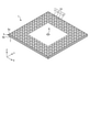
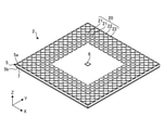
- FIG. 1 is a perspective view of the antenna device 1
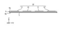
- FIG. 2 is a side view of a part of the antenna device 1.
- the antenna device 1 includes a substrate 5, an antenna element 6, a main plate 7, and a plurality of EBG elements 10.
- the substrate 5 is a dielectric substrate made of, for example, resin, ceramic, or the like.
- An example of a resin is LCP (liquid crystal polymer substrate material).
- the surface of the substrate 5 on the positive direction side of the Z axis is referred to as a main surface 5a and is shown.
- the surface of the substrate 5 on the negative side of the Z axis is referred to as a back surface 5b and is shown.
- the antenna element 6 and the main plate 7 will be described.
- the antenna element 6 transmits (including transmission) and / or receives electromagnetic waves.
- the shape and the like of the antenna element 6 are appropriately determined according to the specifications and the like of the antenna device 1.
- the antenna element 6 is a microstrip antenna (MSL antenna), which is a metal pattern formed on the main surface 5a of the substrate 5.
- the main plate 7 gives a reference potential.
- the main plate 7 is a metal pattern formed on almost the entire surface of the back surface 5b of the substrate 5. Since the antenna element 6 is provided on the main surface 5a of the substrate 5 and the main plate 7 is provided on the back surface 5b of the substrate 5, the antenna device 1 has directivity (main beam) on the main surface 5a side of the substrate 5.
- the plurality of EBG elements 10 are provided side by side on the main surface 5a of the substrate 5 so as to provide an EBG (electromagnetic band gap).
- Each of the plurality of EBG elements 10 is configured to include a metal pattern (corresponding to a patch 10a described later) provided on the main surface 5a of the substrate 5.
- the plurality of EBG elements 10 exemplified have a structure called a mushroom structure or the like, and attenuate (block) electromagnetic waves in a specific frequency band.
- the plurality of EBG elements 10 constitute an electromagnetic wave transmission path and give an attenuation multiplier to an electromagnetic wave in a specific frequency band.
- the frequency band of the electromagnetic wave attenuated by this attenuation multiplier corresponds to EBG.
- the frequency band may be simply referred to as a band.
- a plurality of EBG elements 10 are provided on the main surface 5a of the substrate 5 so as to be separated from the antenna element 6.
- the separation distance between the plurality of EBG elements 10 and the antenna element 6 may be larger than the separation distance between the adjacent EBG elements 10.
- the plurality of EBG elements 10 are collectively arranged in a region spaced from the antenna element 6 at a certain interval.
- the plurality of EBG elements 10 are provided between the antenna element 6 and the edge of the substrate 5.
- the plurality of EBG elements 10 are arranged so as to surround the antenna element 6.
- the electromagnetic wave traveling from the antenna element 6 toward the edge of the substrate 5 traveling in the XY plane direction
- the region where the plurality of EBG elements 10 are provided extends to the edge of the substrate 5. That is, the region where the plurality of EBG elements 10 are provided includes the edge portion of the substrate 5. This makes it easier to secure the arrangement area of the plurality of EBG elements 10.
- the edge portion of the substrate 5 may be defined as, for example, a portion where the EBG elements 10 can be provided side by side in a row along the edge of the substrate 5.
- the electromagnetic wave traveling from the antenna element 6 toward the edge of the substrate 5 is not attenuated and reaches the edge of the substrate 5. At least a part of the electromagnetic wave that has reached the edge of the substrate 5 wraps around to the back surface 5b side of the substrate 5. As a result, electromagnetic waves are radiated in the direction of the back surface 5b of the substrate 5, and unnecessary back lobes are generated. This back lobe is suppressed by the damping effect of the plurality of EBG elements 10 described above.
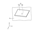
- the EBG element 10 will be further described with reference to FIGS. 3 and 4.
- FIGS. 3 and 4 are diagrams showing an example of a schematic configuration of an EBG element.
- the shape of the exemplified EBG element 10 is similar to the shape of the EBG element 11 among the EBG element 11 and the EBG element 12, but the following description applies to both the EBG element 11 and the EBG element 12.
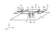
- the illustration of the substrate 5 is omitted in FIG. 4, an example of an equivalent circuit of the EBG element 10 is shown superimposed.
- the EBG element 10 includes a patch 10a and a via 10b.
- the patch 10a is, for example, a metal pattern formed on the main surface 5a of the substrate 5 as described above.
- One end of the via 10b is connected to the patch 10a, the other end is connected to the main plate 7, and the patch 10a is connected to the main plate 7.
- Patches 10a of the EBG element 10 has an inductance in the extending direction (XY plane direction), the inductance constitutes a coil L R of the equivalent circuit.
- the capacitance constitutes a capacitor C L of the equivalent circuit.
- Vias 10b of EBG element 10 has an inductance in the extending direction (Z axis direction), the inductance constitutes a coil L L of the equivalent circuit.
- the element values inductance and capacitance
- attenuation characteristics are attenuation bandwidth, attenuation amount, and the like.
- the value of the element can be adjusted by changing the parameters that define the structure of the plurality of EBG elements 10. Some examples of parameters are described.
- the first example of the parameter is the size (via size) of the via 10b of the EBG element 10. If the via has a circular cross-sectional shape, the via size may be the via diameter. By changing the via size can be adjusted the inductance of the coil L L.
- the second example of the parameter is the size (patch size) of the patch 10a of the EBG element 10.
- the patch size adjustment includes changes in patch length, patch width, patch area, patch shape, and the like.
- patch shapes are circular shapes, polygonal shapes, and the like.
- the third example of the parameter is the spacing between adjacent EBG elements 10, and more specifically, the spacing between adjacent patches 10a (patch spacing). By changing the patch interval, it is possible to adjust the capacitance of the capacitor C L.
- the plurality of EBG elements 10 include a plurality of EBG elements 11 (a plurality of first EBG elements) and a plurality of EBG elements 12 (a plurality of second EBG elements).
- the plurality of EBG elements 12 have a structure different from that of the plurality of EBG elements 11. From the viewpoint of the above-mentioned parameters, the parameters defining the plurality of EBG elements 12 are different from the parameters defining the plurality of EBG elements 11.
- the via size is not particularly shown in FIG. 1, and the via size of each of the plurality of EBG elements 11 and the plurality of EBG elements 12 may be the same or different.
- the patch sizes of the plurality of EBG elements 11 and the plurality of EBG elements 12 are set so that the patch of the EBG element 11 has a quadrangular shape and the patch of the EBG element 12 has a circular shape.
- the patch interval of the plurality of EBG elements 11 and the plurality of EBG elements 12 is set so that each of the plurality of EBG elements 11 and each of the plurality of EBG elements 12 are alternately arranged.
- each of the plurality of EBG elements 11 and each of the plurality of EBG elements 12 are alternately arranged in the X-axis direction and the Y-axis direction.
- the attenuation characteristics given by the plurality of EBG elements 12 are different from the attenuation characteristics given by the plurality of EBG elements 11. Therefore, a damping characteristic having two different damping characteristics can be obtained. For example, the attenuation characteristics are improved, such as a wider attenuation bandwidth and a larger amount of attenuation, as compared with the case where only one attenuation characteristic is given. By improving the damping characteristics, for example, the back robe suppressing effect can be improved.
- a plurality of EBG elements having various structures may be used. An example will be described with reference to FIG.
- FIG. 5 is a diagram showing an example of a schematic configuration of an antenna device according to an embodiment.
- the exemplified antenna device 2 is different from the antenna device 1 (FIG. 1) in that it includes a plurality of EBG elements 20 instead of the plurality of EBG elements 10.
- the plurality of EBG elements 20 include a plurality of EBG elements 21 (a plurality of first EBG elements) and a plurality of EBG elements 22 (a plurality of second EBG elements).
- a plurality of EBG elements 21 surround the antenna element 6, and a plurality of EBG elements 22 surround the plurality of EBG elements 21.
- the via size and the patch size are the same as those of the plurality of EBG elements 11 and the plurality of EBG elements 12 (FIG. 1), so the description thereof will not be repeated.
- the plurality of EBG elements 21 and the plurality of EBG elements 21 and the plurality of EBG elements 22 are provided in order from the antenna element 6 toward the edge of the substrate 5 (in the XY plane direction).
- the patch interval of the EBG element 21 is set.
- the attenuation characteristics are higher than those in the case where only one attenuation characteristic is given. Improve.
- 6 to 10 are diagrams showing an example of a configuration for examining the damping characteristics.
- two antenna elements are provided on the same surface of the substrate, and a plurality of EBG elements are provided between the two antenna elements. This is because the attenuation characteristics given by the plurality of EBG elements can be confirmed by simulating the magnitude of the coupling between the two antenna elements in such a configuration.
- S21 is used in the present disclosure as an index indicating the magnitude of the coupling between the two antenna elements.
- the configuration E1 exemplified in FIGS. 6 and 7 is a configuration for examining the attenuation characteristics given by the EBG element 10 in the antenna device 1 described above with reference to FIG. 1 and the like.
- two antenna elements 61E and antenna elements 62E provided at intervals are provided on the main surface 5Ea of the substrate 5E.
- a plurality of EBG elements 10E are arranged between the antenna element 61E and the antenna element 62E.
- the plurality of EBG elements 10E include a plurality of EBG elements 11E and a plurality of EBG elements 12E.
- the plurality of EBG elements 11E and the plurality of EBG elements 12E are arranged in the same manner as the plurality of EBG elements 11 and the plurality of EBG elements 12 (FIG. 1) except for the number of the elements and the point that they do not surround the antenna element.
- a main plate 7E is provided on the back surface 5Eb of the substrate 5E.
- the relative permittivity of the substrate 5A is 2.97. This relative permittivity is a value assuming LCP.
- the thickness of the substrate 5A is 0.1 mm.
- Both the shape of the antenna element 61E and the shape of the antenna element 62E are quadrangular shapes of 1.042 mm ⁇ 1.042 mm (resonance frequency is about 76 GHz to 77 GHz).
- the conductivity of the metal pattern constituting the main plate 7E, the EBG element 10E, the EBG element 20E, the antenna element 61E, the antenna element 62E, and the main plate 7E is the conductivity of copper.
- the thickness of the metal pattern is 0.043 mm.
- the shape of the patch of the EBG element 11E is a quadrangular shape of 1.031 mm ⁇ 1.031 mm.
- the shape of the patch of the EBG element 12E is a circular shape having a radius of 0.625.
- the vias (not shown) provided on those patches have a radius of 0.05 mm and are provided in the center of the patch.
- the distance D1 between the edges of the adjacent EBG elements 11E and EBG elements 12E is 0.125 mm.
- the distance D2 from the antenna element 61E to the nearest EBG element 11E is 2.714 mm.
- the distance D3 from the antenna element 61E to the nearest EBG element 12E is 2.604 mm.
- the distance from the antenna element 61E to the edge of the substrate 5E is a distance D4 in the X-axis direction of 5.479 mm and a distance D5 in the Y-axis direction of 4.479 mm.
- the configurations shown in FIGS. 8 to 10 below are the same except for the parts different from the configuration E1, and the configurations of the different parts can be inferred, so the description thereof will be omitted.
- the configuration E2 exemplified in FIG. 8 is a configuration for examining the attenuation characteristics given by the EBG element 20 in the antenna device 2 described above with reference to FIG.
- the configuration E2 includes a plurality of EBG elements 20E instead of the plurality of EBG elements 10E (FIG. 7) as compared with the configuration E1.
- the plurality of EBG elements 20E include a plurality of EBG elements 21E and a plurality of EBG elements 22E.
- the plurality of EBG elements 21E and the plurality of EBG elements 22E are arranged in the same manner as the plurality of EBG elements 21 and the plurality of EBG elements 22 (FIG. 5) except that the number of the elements thereof and the point that they do not surround the antenna element. To.
- Configuration E3 exemplified in FIG. 9 is a configuration of a comparative example.
- the configuration E3 includes a plurality of EBG elements 30E instead of the plurality of EBG elements 20E as compared with the configuration E2.
- the plurality of EBG elements 30E are the same as the plurality of EBG elements 21E (FIG. 8), and do not have a configuration corresponding to the plurality of EBG elements 22E.
- Configuration E4 exemplified in FIG. 10 is a configuration of a comparative example.
- the configuration E4 includes a plurality of EBG elements 40E instead of the plurality of EBG elements 20E as compared with the configuration E2.
- the plurality of EBG elements 40 are the same as the plurality of EBG elements 22E (FIG. 8), and do not have a configuration corresponding to the plurality of EBG elements 21E.
- 11 and 12 are diagrams showing examples of simulation results.
- the horizontal axis of the graph shows the frequency
- the vertical axis of the graph shows S21 (dB) from the antenna element 61E to the antenna element 62E.
- the frequency range is 65 GHz to 85 GHz.
- the graph line C0 shown in FIG. 11 indicates S21 when a plurality of EBG elements do not exist.
- Graph lines C1 to C4 indicate S21 of configurations E1 to E4.
- the graph lines C1 to C4 shown in FIG. 12 show the relative values of S21 of the configurations E1 to E4 when S21 is used as a reference when a plurality of EBG elements are not present.
- electromagnetic waves are attenuated to some extent in any of the configurations E1 to E4.
- the attenuation of the electromagnetic wave as a whole is determined in the configuration E3 and the configuration E4 in both the configuration E1 and the configuration E2, although the variation in the direction in which the attenuation is weakened is included in the configuration E2.
- the attenuation amount in the configuration E1 is further larger than the attenuation amount in the configuration E2, and the attenuation characteristic in the configuration E1 is further improved than the attenuation characteristic in the configuration E2.
- the improvement of the attenuation characteristics in the configuration E1 and the configuration E2 indicates the improvement of the attenuation characteristics in the antenna device 1 and the antenna device 2. From this, it can be seen that the antenna device 1 and the antenna device 2 improve the attenuation characteristics.
- the antenna device according to the embodiment described above is mounted on, for example, a radar device and used. This will be described with reference to FIG.
- FIG. 13 is a diagram showing an example of a schematic configuration of a radar device.
- the radar device 8 includes a transmitting unit 81, an antenna device 82, an antenna device 83, a receiving unit 84, and a control unit 85.
- the transmission unit 81 performs transmission processing.
- the transmission process may include modulation process, frequency conversion process (up-conversion), amplification process, filtering process and the like.
- modulation is FM modulation, but various other modulations suitable for radar may be used.
- the antenna device 82 and the antenna device 83 will be described.
- the antenna device 82 transmits (radiates) a transmission signal.
- the antenna device 83 receives a part of the transmission signal transmitted from the antenna device 82 and reflected by an object (not shown). Examples of objects are vehicles, people, buildings, and so on.
- the antenna device 1 (FIG. 1) or the antenna device 2 (FIG. 5) described above may be used.
- the receiving unit 84 performs reception processing.
- the reception process may include amplification process, filtering process, frequency conversion process (down conversion), demodulation process and the like.
- the control unit 85 controls the entire radar device 8.
- the control by the control unit 85 includes the control of the transmission process by the transmission unit 81 and the control of the reception process by the reception unit 84.
- the control unit 85 detects, for example, the distance to the object (distance measurement) or the orientation of the object (positioning).
- FIG. 13 illustrates the distance measurement positioning unit 85a. Since the method of distance measurement and positioning itself is known, detailed description thereof will be omitted here.
- the configuration of the radar device 8 described above is an example and may be changed as appropriate.
- the antenna device 82 and the antenna device 83 may be configured by one antenna configured so that transmission / reception can be switched.
- the back robe suppression effect is improved, so that distance measurement positioning can be performed even for a distant object by increasing the energy of the main beam by that amount. become.
- the distance measurement positioning accuracy is improved. Therefore, the performance of the radar device 8 can be improved.
- the technology according to this disclosure can be applied to various products.
- the technique according to the present disclosure may be realized as a device mounted on any type of vehicle such as an automobile, an electric vehicle, a hybrid electric vehicle, and a motorcycle.
- FIG. 14 is a block diagram showing an example of a schematic configuration of a vehicle control system 2000 to which the technique according to the present disclosure can be applied.
- the vehicle control system 2000 includes a plurality of electronic control units connected via a communication network 2010.
- the vehicle control system 2000 includes a drive system control unit 2100, a body system control unit 2200, a battery control unit 2300, an outside information detection device 2400, an in-vehicle information detection device 2500, and an integrated control unit 2600. ..
- the communication network 2010 connecting these multiple control units conforms to any standard such as CAN (Controller Area Network), LIN (Local Interconnect Network), LAN (Local Area Network) or FlexRay (registered trademark). It may be an in-vehicle communication network.
- Each control unit includes a microcomputer that performs arithmetic processing according to various programs, a storage unit that stores programs executed by the microcomputer or parameters used for various arithmetic, and a drive circuit that drives various controlled devices. To prepare for.
- Each control unit is provided with a network I / F for communicating with other control units via the communication network 2010, and is connected to devices or sensors inside and outside the vehicle by wired communication or wireless communication.
- a communication I / F for performing communication is provided. In FIG.
- control units also include a microcomputer, a communication I / F, a storage unit, and the like.
- the drive system control unit 2100 controls the operation of the device related to the drive system of the vehicle according to various programs.
- the drive system control unit 2100 has a driving force generator for generating a driving force of a vehicle such as an internal combustion engine or a driving motor, a driving force transmission mechanism for transmitting the driving force to the wheels, and a steering angle of the vehicle. It functions as a control device such as a steering mechanism for adjusting and a braking device for generating braking force of the vehicle.
- the drive system control unit 2100 may have a function as a control device such as ABS (Antilock Brake System) or ESC (Electronic Stability Control).
- the vehicle state detection unit 2110 is connected to the drive system control unit 2100.
- the vehicle state detection unit 2110 may include, for example, a gyro sensor that detects the angular velocity of the axial rotation motion of the vehicle body, an acceleration sensor that detects the acceleration of the vehicle, an accelerator pedal operation amount, a brake pedal operation amount, or steering wheel steering. It includes at least one of sensors for detecting an angle, engine speed, wheel speed, and the like.
- the drive system control unit 2100 performs arithmetic processing using a signal input from the vehicle state detection unit 2110 to control an internal combustion engine, a drive motor, an electric power steering device, a brake device, and the like.
- the body system control unit 2200 controls the operation of various devices mounted on the vehicle body according to various programs.
- the body system control unit 2200 functions as a keyless entry system, a smart key system, a power window device, or a control device for various lamps such as headlamps, back lamps, brake lamps, turn signals or fog lamps.
- a radio wave transmitted from a portable device that substitutes for a key or signals of various switches may be input to the body system control unit 2200.
- the body system control unit 2200 receives inputs of these radio waves or signals and controls a vehicle door lock device, a power window device, a lamp, and the like.
- the battery control unit 2300 controls the secondary battery 2310, which is the power supply source of the drive motor, according to various programs. For example, information such as the battery temperature, the battery output voltage, or the remaining capacity of the battery is input to the battery control unit 2300 from the battery device including the secondary battery 2310. The battery control unit 2300 performs arithmetic processing using these signals, and controls the temperature control of the secondary battery 2310 or the cooling device provided in the battery device.
- the outside information detection device 2400 detects information outside the vehicle equipped with the vehicle control system 2000.
- the image pickup unit 2410 and the vehicle exterior information detection unit 2420 is connected to the vehicle exterior information detection device 2400.
- the image pickup unit 2410 includes at least one of a ToF (Time Of Flight) camera, a stereo camera, a monocular camera, an infrared camera, and other cameras.
- the vehicle outside information detection unit 2420 is used, for example, to detect the current weather or an environment sensor for detecting the weather, or other vehicles, obstacles, pedestrians, etc. around the vehicle equipped with the vehicle control system 2000. Includes ambient information detection sensors.
- the environment sensor may be, for example, at least one of a raindrop sensor that detects rainy weather, a fog sensor that detects fog, a sunshine sensor that detects the degree of sunshine, and a snow sensor that detects snowfall.
- the ambient information detection sensor may be at least one of an ultrasonic sensor, a radar device, and a LIDAR (Light Detection and Ranging, Laser Imaging Detection and Ranging) device.
- the image pickup unit 2410 and the vehicle exterior information detection unit 2420 may be provided as independent sensors or devices, or may be provided as a device in which a plurality of sensors or devices are integrated.
- FIG. 15 shows an example of the installation position of the image pickup unit 2410 and the vehicle outside information detection unit 2420.
- the image pickup units 2910, 2912, 2914, 2916, and 2918 are provided, for example, at at least one of the front nose, side mirrors, rear bumpers, back doors, and the upper part of the windshield in the vehicle interior of the vehicle 2900.
- the image pickup unit 2910 provided in the front nose and the image pickup section 2918 provided in the upper part of the windshield in the vehicle interior mainly acquire an image in front of the vehicle 2900.
- the image pickup units 2912 and 2914 provided in the side mirrors mainly acquire images of the side of the vehicle 2900.
- the image pickup unit 2916 provided in the rear bumper or the back door mainly acquires an image of the rear of the vehicle 2900.
- the image pickup unit 2918 provided on the upper part of the windshield in the vehicle interior is mainly used for detecting a preceding vehicle, a pedestrian, an obstacle, a traffic light, a traffic sign, a lane, or
- FIG. 15 shows an example of the shooting range of each of the imaging units 2910, 2912, 2914, and 2916.
- the imaging range a indicates the imaging range of the imaging unit 2910 provided on the front nose
- the imaging ranges b and c indicate the imaging ranges of the imaging units 2912 and 2914 provided on the side mirrors, respectively
- the imaging range d indicates the imaging range d.
- the imaging range of the imaging unit 2916 provided on the rear bumper or the back door is shown. For example, by superimposing the image data captured by the image pickup units 2910, 2912, 2914, and 2916, a bird's-eye view image of the vehicle 2900 as viewed from above can be obtained.
- the vehicle exterior information detection unit 2920, 2922, 2924, 2926, 2928, 2930 provided at the front, rear, side, corner and the upper part of the windshield of the vehicle interior of the vehicle 2900 may be, for example, an ultrasonic sensor or a radar device.
- the vehicle exterior information detection units 2920, 2926, 2930 provided on the front nose, rear bumper, back door, and upper part of the windshield in the vehicle interior of the vehicle 2900 may be, for example, a lidar device.
- These out-of-vehicle information detection units 2920 to 2930 are mainly used for detecting a preceding vehicle, a pedestrian, an obstacle, or the like.
- the vehicle outside information detection device 2400 causes the image pickup unit 2410 to capture an image of the outside of the vehicle and receives the captured image data. Further, the vehicle outside information detection device 2400 receives detection information from the connected vehicle outside information detection unit 2420.
- the vehicle exterior information detection unit 2420 is an ultrasonic sensor, a radar device, or a lidar device
- the vehicle exterior information detection device 2400 transmits ultrasonic waves, electromagnetic waves, or the like, and receives the received reflected wave information.
- the out-of-vehicle information detection device 2400 may perform object detection processing or distance detection processing such as a person, a vehicle, an obstacle, a sign, or a character on the road surface based on the received information.
- the out-of-vehicle information detection device 2400 may perform an environment recognition process for recognizing rainfall, fog, road surface conditions, etc. based on the received information.
- the out-of-vehicle information detection device 2400 may calculate the distance to an object outside the vehicle based on the received information.
- the vehicle outside information detection device 2400 may perform image recognition processing or distance detection processing for recognizing a person, a vehicle, an obstacle, a sign, a character on the road surface, or the like based on the received image data.
- the vehicle outside information detection device 2400 performs processing such as distortion correction or alignment on the received image data, and synthesizes the image data captured by different image pickup units 2410 to generate a bird's-eye view image or a panoramic image. May be good.
- the vehicle exterior information detection device 2400 may perform the viewpoint conversion process using the image data captured by different image pickup units 2410.
- the in-vehicle information detection device 2500 detects the in-vehicle information.
- a driver state detection unit 2510 that detects the state of the driver is connected to the in-vehicle information detection device 2500.
- the driver state detection unit 2510 may include a camera that captures the driver, a biosensor that detects the driver's biological information, a microphone that collects sound in the vehicle interior, and the like.
- the biosensor is provided on, for example, a seat surface or a steering wheel, and detects biometric information of a passenger sitting on the seat or a driver holding the steering wheel.
- the in-vehicle information detection device 2500 may calculate the degree of fatigue or concentration of the driver based on the detection information input from the driver state detection unit 2510, and determines whether or not the driver is dozing. You may.
- the in-vehicle information detection device 2500 may perform processing such as noise canceling processing on the collected audio signal.
- the integrated control unit 2600 controls the overall operation in the vehicle control system 2000 according to various programs.
- An input unit 2800 is connected to the integrated control unit 2600.
- the input unit 2800 is realized by a device that can be input-operated by the passenger, such as a touch panel, a button, a microphone, a switch, or a lever.
- the input unit 2800 may be, for example, a remote control device using infrared rays or other radio waves, or an external connection device such as a mobile phone or a PDA (Personal Digital Assistant) corresponding to the operation of the vehicle control system 2000. You may.
- the input unit 2800 may be, for example, a camera, in which case the passenger can input information by gesture.
- the input unit 2800 may include, for example, an input control circuit that generates an input signal based on the information input by the passenger or the like using the input unit 2800 and outputs the input signal to the integrated control unit 2600.
- an input control circuit that generates an input signal based on the information input by the passenger or the like using the input unit 2800 and outputs the input signal to the integrated control unit 2600.
- the storage unit 2690 may include a RAM (Random Access Memory) for storing various programs executed by the microcomputer, and a ROM (Read Only Memory) for storing various parameters, calculation results, sensor values, and the like. Further, the storage unit 2690 may be realized by a magnetic storage device such as an HDD (Hard Disc Drive), a semiconductor storage device, an optical storage device, an optical magnetic storage device, or the like.
- a RAM Random Access Memory
- ROM Read Only Memory
- the storage unit 2690 may be realized by a magnetic storage device such as an HDD (Hard Disc Drive), a semiconductor storage device, an optical storage device, an optical magnetic storage device, or the like.
- the general-purpose communication I / F 2620 is a general-purpose communication I / F that mediates communication with various devices existing in the external environment 2750.
- the general-purpose communication I / F2620 is a cellular communication protocol such as GSM (Global System of Mobile communications) (registered trademark), WiMAX, LTE (Long Term Evolution) or LTE-A (LTE-Advanced), or wireless LAN (Wi-Fi).
- GSM Global System of Mobile communications
- WiMAX Wireless F
- LTE Long Term Evolution
- LTE-A Long Term Evolution-A
- Wi-Fi wireless LAN
- Other wireless communication protocols such as (also referred to as (registered trademark)) may be implemented.
- the general-purpose communication I / F 2620 connects to a device (for example, an application server or a control server) existing on an external network (for example, the Internet, a cloud network or a business-specific network) via a base station or an access point, for example. You may. Further, the general-purpose communication I / F2620 is connected to a terminal existing in the vicinity of the vehicle (for example, a pedestrian or store terminal, or an MTC (Machine Type Communication) terminal) by using, for example, P2P (Peer To Peer) technology. You may.
- the dedicated communication I / F 2630 is a communication I / F that supports a communication protocol formulated for use in a vehicle.
- the dedicated communication I / F2630 may implement a standard protocol such as WAVE (Wireless Access in Vehicle Environment) or DSRC (Dedicated Short Range Communications), which is a combination of the lower layer IEEE802.11p and the upper layer IEEE1609. ..
- Dedicated communication I / F2630 is typically a concept that includes one or more of vehicle-to-vehicle (Vehicle to Vehicle) communication, road-to-vehicle (Vehicle to Infrastructure) communication, and pedestrian-to-vehicle (Vehicle to Pedestrian) communication. Carry out communication.
- the positioning unit 2640 receives, for example, a GNSS signal from a GNSS (Global Navigation Satellite System) satellite (for example, a GPS signal from a GPS (Global Positioning System) satellite), executes positioning, and executes positioning, and the latitude, longitude, and altitude of the vehicle. Generate location information including.
- the positioning unit 2640 may specify the current position by exchanging signals with the wireless access point, or may acquire position information from a terminal such as a mobile phone, PHS, or smartphone having a positioning function.
- the beacon receiving unit 2650 receives, for example, a radio wave or an electromagnetic wave transmitted from a radio station or the like installed on a road, and acquires information such as a current position, a traffic jam, a road closure, or a required time.
- the function of the beacon receiving unit 2650 may be included in the above-mentioned dedicated communication I / F 2630.
- the in-vehicle device I / F2660 is a communication interface that mediates the connection between the microcomputer 2610 and various devices existing in the vehicle.
- the in-vehicle device I / F2660 may establish a wireless connection using a wireless communication protocol such as wireless LAN, Bluetooth (registered trademark), NFC (Near Field Communication) or WUSB (Wireless USB). Further, the in-vehicle device I / F2660 may establish a wired connection via a connection terminal (and a cable if necessary) (not shown).
- the in-vehicle device I / F2660 exchanges control signals or data signals with, for example, a passenger's mobile device or wearable device, or an information device carried in or attached to the vehicle.
- the in-vehicle network I / F2680 is an interface that mediates communication between the microcomputer 2610 and the communication network 2010.
- the in-vehicle network I / F2680 transmits / receives signals and the like according to a predetermined protocol supported by the communication network 2010.
- the microcomputer 2610 of the integrated control unit 2600 is via at least one of a general-purpose communication I / F2620, a dedicated communication I / F2630, a positioning unit 2640, a beacon receiving unit 2650, an in-vehicle device I / F2660, and an in-vehicle network I / F2680.
- the vehicle control system 2000 is controlled according to various programs based on the information acquired.
- the microcomputer 2610 calculates the control target value of the driving force generator, the steering mechanism, or the braking device based on the acquired information inside and outside the vehicle, and outputs a control command to the drive system control unit 2100. May be good.
- the microcomputer 2610 may perform coordinated control for the purpose of collision avoidance or impact mitigation of a vehicle, follow-up traveling based on an inter-vehicle distance, vehicle speed maintenance traveling, automatic driving, and the like.
- the microcomputer 2610 has information acquired via at least one of a general-purpose communication I / F2620, a dedicated communication I / F2630, a positioning unit 2640, a beacon receiving unit 2650, an in-vehicle device I / F2660, and an in-vehicle network I / F2680. Based on the above, local map information including information on the surroundings of the current position of the vehicle may be created. Further, the microcomputer 2610 may predict the danger of a vehicle collision, a pedestrian or the like approaching or entering a closed road, and generate a warning signal based on the acquired information.
- the warning signal may be, for example, a signal for generating a warning sound or lighting a warning lamp.
- the audio image output unit 2670 transmits an output signal of at least one of audio and image to an output device capable of visually or audibly notifying information to the passenger or the outside of the vehicle.
- an audio speaker 2710, a display unit 2720, and an instrument panel 2730 are exemplified as output devices.
- the display unit 2720 may include, for example, at least one of an onboard display and a head-up display.
- the display unit 2720 may have an AR (Augmented Reality) display function.
- the output device may be another device other than these devices, such as headphones, a projector, or a lamp.
- the display device displays the results obtained by various processes performed by the microcomputer 2610 or the information received from other control units in various formats such as texts, images, tables, and graphs. Display visually.
- the audio output device converts an audio signal composed of reproduced audio data, acoustic data, or the like into an analog signal and outputs the audio signal audibly.
- At least two control units connected via the communication network 2010 may be integrated as one control unit.
- each control unit may be composed of a plurality of control units.
- the vehicle control system 2000 may include another control unit (not shown).
- the other control unit may have a part or all of the functions carried out by any of the control units. That is, as long as information is transmitted and received via the communication network 2010, predetermined arithmetic processing may be performed by any of the control units.
- a sensor or device connected to any control unit may be connected to another control unit, and a plurality of control units may send and receive detection information to and from each other via the communication network 2010. ..
- the antenna device 1 and the antenna device 2 according to the present embodiment described with reference to FIGS. 1 and 5, and the radar device according to the present embodiment described with reference to FIG. 13 and the like. 8 can be applied to the vehicle exterior information detection unit 2420 of the application example shown in FIG. That is, by using the antenna device 1, the antenna device 2, or the radar device 8 having an improved bucklobe suppression effect, for example, the detection performance can be improved.
- the antenna device 1 includes an antenna element 6 and a plurality of EBG elements 10.
- the plurality of EBG elements 10 include a plurality of EBG elements 11 and a plurality of EBG elements 12 having a structure different from that of the plurality of EBG elements 11.
- the attenuation characteristics given by the plurality of EBG elements 12 are the attenuation characteristics given by the plurality of EBG elements 11. Is different. Therefore, a damping characteristic having two different damping characteristics can be obtained. For example, the attenuation characteristics are improved, such as a wider attenuation bandwidth and a larger amount of attenuation, as compared with the case where only one attenuation characteristic is given. By improving the damping characteristics, for example, the effect of suppressing the back lobe can be improved.
- the plurality of EBG elements 10 may surround the antenna element 6. Thereby, in the plane including the antenna element 6 and the EBG element 10 (for example, the XY plane), the electromagnetic wave traveling from the antenna element 6 toward the plane can be attenuated.
- each of the plurality of EBG elements 11 and each of the plurality of EBG elements 12 may be arranged alternately. For example, in this way, a plurality of EBG elements 11 and a plurality of EBG elements 12 having different structures can be arranged.
- the plurality of EBG elements 21 may surround the antenna element 6, and the plurality of EBG elements 22 may surround the EBG element 21. In this way, a plurality of EBG elements 21 and a plurality of EBG elements 22 having different structures can be arranged.
- the antenna element 6 and the plurality of EBG elements 10 may be arranged on the main surface 5a of the substrate 5.
- the antenna device 1 can be used as a planar antenna. There are merits such as making the antenna device 1 compact.
- the plurality of EBG elements 11 are provided apart from the antenna element 6, and the separation distance between the plurality of EBG elements 10 and the antenna element 6 is such that the adjacent EBG elements 11 are separated from each other. It may be larger than the separation distance of. As a result, the main beam can have a certain width.
- the region where the plurality of EBG elements 11 are provided may include the edge portion of the substrate 5. This makes it easier to secure the arrangement area of the plurality of EBG elements 10.
- each of the plurality of EBG elements 10 includes a patch 10a provided on the main surface 5a of the substrate 5 and a main plate provided on the back surface 5b of the substrate 5. 7 and a via 10b connecting the patch 10a may be included.
- a plurality of EBG elements 10 can be incorporated into a planar antenna.
- the parameters defining the structure of the plurality of EBG elements 10 include at least one of the size of the patch 10a, the size of the via 10b, and the spacing between the patches 10a of the adjacent EBG elements 10, and the plurality of EBG elements 12
- the parameters defining the structure of the EBG element 11 may be different from the parameters defining the structure of the plurality of EBG elements 11.
- the plurality of EBG elements 12 can have a structure different from that of the plurality of EBG elements 11.
- the antenna device 82 and the antenna device 83 may be mounted on the radar device 8. Thereby, the performance of the radar device 8 can be improved.
- the antenna device may be mounted on the vehicle. As a result, the detection performance of the vehicle outside information detection unit can be improved.
- FIGS. 16 and 17 are diagrams showing examples of simulation results.
- FIG. 16 shows the simulation result of directivity at a frequency of 76 GHz.
- the upper side of the graph shows the directivity of the main surface 5a side (Z-axis positive direction side) of the substrate 5, and the lower side of the graph shows the directivity of the back surface 5b side (Z-axis negative direction side) of the substrate 5.
- the graph line G0 shows the directivity of the configuration in which the plurality of EBG elements 10 do not exist in the antenna device 1 (FIG. 1).
- the graph line G1 shows the directivity of the configuration in which a plurality of EBG elements 11 and a plurality of EBG elements 12 are mixed as in the antenna device 1.
- the graph line G2 shows the directivity of the configuration in which the plurality of EBG elements 10 are all the plurality of EBG elements 11 in the antenna device 1.
- the horizontal axis of the graph in FIG. 17 indicates the frequency, and the vertical axis of the graph indicates the backside radiation amount (dB).
- the horizontal axis of the graph shows the frequency, and the vertical axis of the graph shows the backside radiation amount (dB) based on the radiation amount of the configuration in which the plurality of EBG elements 10 do not exist in the antenna device 1.
- the back surface of the substrate 5 is the case where the EBG element is present (graph line G1 and the graph line G2) as compared with the case where the EBG element is not present (graph line G0). It can be seen that the amount of radiation to the 5b side is reduced. Further, the configuration including the plurality of EBG elements 11 and the plurality of EBG elements 12 having different structures (graph line G1) emits more radiation than the configuration including only the plurality of EBG elements 11 having the same structure (graph line G2). It can be seen that the band where the amount is small is widened (in this example, around 74 GHz).
- the plurality of EBG elements may include a plurality of three or more types of EBG elements, each of which has a different structure.
- the present technology can also have the following configurations.
- Antenna element and With multiple EBG elements Equipped with The plurality of EBG elements are With a plurality of first EBG elements,
- the plurality of first EBG elements include a plurality of second EBG elements having different structures. including, Antenna device.
- the plurality of EBG elements surround the antenna element.
- the antenna device according to (1) (3)
- Each of the plurality of first EBG elements and each of the plurality of second EBG elements are alternately arranged.
- (4) The plurality of first EBG elements surround the antenna element.
- the plurality of second EBG elements surround the plurality of first EBG elements.
- the antenna element and the plurality of EBG elements are arranged on the main surface of the substrate.
- the plurality of EBG elements are provided apart from the antenna element.
- the separation distance between the plurality of EBG elements and the antenna element is larger than the separation distance between adjacent EBG elements among the plurality of EBG elements.
- the region where the plurality of EBG elements are provided includes the edge portion of the substrate.
- Each of the plurality of EBG elements A patch provided on the main surface of the substrate and A main plate provided on the back surface of the substrate and a via connecting the patch, including, The antenna device according to any one of (5) to (7).
- the parameters defining the structure of the plurality of EBG elements include at least one of the patch size, the via size, and the spacing between the patches of the adjacent EBG elements.
- the parameter defining the structure of the plurality of second EBG elements is different from the parameter defining the plurality of first EBG elements.
- Antenna device 2 Antenna device 5 Board 6 Antenna element 7 Main plate 8 Radar device 10 EBG element 11 EBG element 12 EBG element 20 EBG element 21 EBG element 22 EBG element 81 Transmitter 82 Antenna device 83 Antenna device 84 Receiver 85 Distance measurement positioning unit
Landscapes
- Engineering & Computer Science (AREA)
- Radar, Positioning & Navigation (AREA)
- Remote Sensing (AREA)
- Physics & Mathematics (AREA)
- Computer Security & Cryptography (AREA)
- Computer Networks & Wireless Communication (AREA)
- General Physics & Mathematics (AREA)
- Optics & Photonics (AREA)
- Waveguide Aerials (AREA)
- Radar Systems Or Details Thereof (AREA)
Abstract
アンテナ装置(1)は、アンテナ素子(6)と、複数のEBG素子(10)と、を備え、複数のEBG素子(10)は、複数の第1のEBG素子(11)と、複数の第1のEBG素子(11)は異なる構造を有する複数の第2のEBG素子(12)と、を含む。
Description
本開示は、アンテナ装置に関する。
電磁波を減衰させるために、電磁バンドギャップ(EBG:Electromagnetic Band Gap)素子が用いられることが知られている。例えば特許文献1は、EBG素子を用いてアンテナ間アイソレーションを確保する手法を開示する。
EBG素子によって得られる電磁波の減衰特性が十分でない場合がある。この問題について、特許文献1では検討は行われていない。
本開示の一側面は、EBG素子による減衰特性を改善することが可能なアンテナ装置を提供することを目的とする。
本開示の一側面に係るアンテナ装置は、アンテナ素子と、複数のEBG素子と、を備え、複数のEBG素子は、複数の第1のEBG素子と、複数の第1のEBG素子は異なる構造を有する複数の第2のEBG素子と、を含む。
以下に、本開示の実施形態について図面に基づいて詳細に説明する。なお、以下の各実施形態において、同一の部位には同一の符号を付することにより重複する説明を省略する。
以下に示す項目順序に従って本開示を説明する。
1. 実施形態
2. 応用例
3. 効果
1. 実施形態
2. 応用例
3. 効果
1. 実施形態
図1及び図2は、実施形態に係るアンテナ装置の概略構成の例を示す図である。例示されるアンテナ装置1は、平面アンテナであり、基板5に設けられる。図にはXYZ座標が示される。X軸方向及びY軸方向は、基板5の面方向に相当する。Z軸方向は、基板5の厚さ方向に相当する。図1はアンテナ装置1の斜視図であり、図2はアンテナ装置1の一部の側面図である。アンテナ装置1は、基板5と、アンテナ素子6と、地板7と、複数のEBG素子10とを含む。
図1及び図2は、実施形態に係るアンテナ装置の概略構成の例を示す図である。例示されるアンテナ装置1は、平面アンテナであり、基板5に設けられる。図にはXYZ座標が示される。X軸方向及びY軸方向は、基板5の面方向に相当する。Z軸方向は、基板5の厚さ方向に相当する。図1はアンテナ装置1の斜視図であり、図2はアンテナ装置1の一部の側面図である。アンテナ装置1は、基板5と、アンテナ素子6と、地板7と、複数のEBG素子10とを含む。
基板5は、例えば樹脂、セラミック等で構成される誘電体基板である。樹脂の一例は、LCP(液晶ポリマ基板材)である。基板5のZ軸正方向側の面を、主面5aと称し図示する。基板5のZ軸負方向側の面を、裏面5bと称し図示する。
アンテナ素子6及び地板7について説明する。アンテナ素子6は、電磁波の送信(発信を含む)及び/又は受信を行う。アンテナ素子6の形状等は、アンテナ装置1の仕様等に応じて適宜定められる。この例では、アンテナ素子6は、マイクロストリップアンテナ(MSLアンテナ)であり、基板5の主面5a上に形成された金属パターンである。地板7は、基準電位を与える。この例では、地板7は、基板5の裏面5bのほぼ全面上に形成された金属パターンである。アンテナ素子6が基板5の主面5aに設けられ、地板7が基板5の裏面5bに設けられるので、アンテナ装置1は、基板5の主面5a側に指向性(主ビーム)を有する。
複数のEBG素子10は、EBG(電磁バンドギャップ)を与えるように、基板5の主面5a上に並んで設けられる。複数のEBG素子10の各々は、基板5の主面5a上に設けられた金属パターン(後述のパッチ10aに相当)を含んで構成される。例示される複数のEBG素子10は、マッシュルーム構造等と称される構造を有し、特定の周波数帯域の電磁波を減衰させる(遮断する)。具体的に、複数のEBG素子10は、電磁波の伝送経路を構成するとともに、特定の周波数帯域の電磁波に対して減衰乗数を与える。この減衰乗数によって減衰する電磁波の周波数帯域が、EBGに相当する。なお、以下では、周波数帯域を、単に帯域という場合もある。
基板5の主面5a上において、複数のEBG素子10は、アンテナ素子6から離間して設けられる。複数のEBG素子10がアンテナ素子6からある程度離れて配置されることで、アンテナ素子6本来の放射特性への影響(指向性変化、アンテナ共振周波数ずれ等)を低減することができる。複数のEBG素子10とアンテナ素子6との離間距離は、隣り合うEBG素子10どうしの離間距離よりも大きくてよい。図1に示される例では、複数のEBG素子10は、アンテナ素子6から一定の間隔をあけた領域内に集約して配置される。複数のEBG素子10は、アンテナ素子6と、基板5の縁との間に設けられる。この例では、複数のEBG素子10は、アンテナ素子6を囲むように配置される。これにより、アンテナ素子6から基板5の縁に向かって進む(XY平面方向に進む)電磁波が、複数のEBG素子10が設けられた領域で減衰する。また、図1に示される例では、複数のEBG素子10が設けられる領域は、基板5の縁まで延在する。すなわち、複数のEBG素子10が設けられる領域は、基板5の縁部を含む。これにより、複数のEBG素子10の配置面積が確保しやすくなる。基板5縁部は、例えば、基板5の縁に沿ってEBG素子10が一列に並んで設けることが可能な部分として定められてよい。
仮に複数のEBG素子10が設けられていないと、アンテナ素子6から基板5の縁に向かって進む電磁波が減衰せずに基板5の縁に至る。基板5の縁に到達した電磁波の少なくとも一部は、基板5の裏面5b側に回り込む。その結果、基板5の裏面5b方向に電磁波が放射され、不要なバックローブが発生する。このバックローブは、上述の複数のEBG素子10による減衰効果により抑制される。EBG素子10について、図3及び図4も参照してさらに説明する。
図3及び図4は、EBG素子の概略構成の例を示す図である。例示されるEBG素子10の形状は、EBG素子11及びEBG素子12のうちEBG素子11の形状に類似するが、以下の説明は、EBG素子11及びEBG素子12の両方に適用される。なお、図4には、基板5の図示が省略される一方で、EBG素子10の等価回路の例が重ねて示される。図3及び図4に示されるように、EBG素子10は、パッチ10aと、ビア10bとを含む。パッチ10aは、例えば先に述べたように基板5の主面5a上に形成された金属パターンである。ビア10bは、一端がパッチ10aに接続され他端が地板7に接続され、パッチ10aを地板7に接続する。
EBG素子10のパッチ10aは、その延在方向(XY平面方向)にインダクタンスを有し、このインダクタンスが、等価回路のコイルLRを構成する。
隣り合うEBG素子10のパッチ10aどうしは、キャパシタンスを形成し、このキャパシタンスが、等価回路のコンデンサCLを構成する。
EBG素子10のビア10bは、延在方向(Z軸方向)にインダクタンスを有し、このインダクタンスが、等価回路のコイルLLを構成する。
EBG素子10のパッチ10a及び地板7は、キャパシタンスを与え、このキャパシタンスが、等価回路のCRを構成する。
複数のEBG素子10が並んで設けられるので、コンデンサCL及びコイルLRのLC直列回路が、その直列方向に繰り返し存在する。各LC直列回路は、コイルLL及びコンデンサCRの並列回路を介して、地板7に接続される。したがって、図4に示される等価回路が得られる。
例えば上述の等価回路における素子の値(インダクタンス及びキャパシタンス)を調整することで、複数のEBG素子10による電磁波の減衰特性を設計できる。減衰特性の例は、減衰帯域幅、減衰量等である。素子の値は、複数のEBG素子10の構造を規定するパラメータを変えることで調整できる。パラメータのいくつかの例について説明する。
パラメータの第1の例は、EBG素子10のビア10bの大きさ(ビアサイズ)である。ビアが円形断面形状を有する場合、ビアサイズは、ビア径であってよい。ビアサイズを変えることで、コイルLLのインダクタンスを調整できる。
パラメータの第2の例は、EBG素子10のパッチ10aの大きさ(パッチサイズ)である。パッチサイズを変えることで、コイルLRのインダクタンス及びコンデンサCRのキャパシタンスを調整できる。パッチサイズの調整は、パッチ長さ、パッチ幅、パッチ面積、パッチ形状等の変更を含む。パッチの形状の例は、円形形状、多角形形状等である。
パラメータの第3の例は、隣り合うEBG素子10どうしの間隔であり、より具体的には隣り合うパッチ10aどうしの間隔(パッチ間隔)である。パッチ間隔を変えることで、コンデンサCLのキャパシタンスを調整できる。
例えば以上説明したようなパラメータを調整することとで、複数のEBG素子10による減衰特性を設計することができる。ここで、複数のEBG素子10が単一の構造を有すると、例えば減衰帯域幅が狭過ぎたり、減衰量が小さ過ぎたりする等、十分な減衰特性が得られない場合がある。減衰特性が十分でないと、例えばバックローブ抑制効果も低減する。そこで、アンテナ装置1では、複数のEBG素子10が、複数のEBG素子11(複数の第1のEBG素子)と、複数のEBG素子12(複数の第2のEBG素子)とを含む。複数のEBG素子12は、複数のEBG素子11とは異なる構造を有する。上述のパラメータの観点から述べると、複数のEBG素子12を規定するパラメータが、複数のEBG素子11を規定するパラメータとは異なる。
パラメータのうち、上記で例示したビアサイズ、パッチサイズ及びパッチ間隔の3つのパラメータについて述べる。ビアサイズに関して、図1にはとくに図示されておらず、複数のEBG素子11及び複数のEBG素子12それぞれのビアサイズは、同じであってもよいしい異なっていてもよい。
パッチサイズに関して、EBG素子11のパッチが四角形形状を有し、EBG素子12のパッチが円形形状を有するように、複数のEBG素子11及び複数のEBG素子12のパッチサイズが設定される。
パッチ間隔に関して、複数のEBG素子11の各々と複数のEBG素子12の各々とが交互に配置されるように、複数のEBG素子11及び複数のEBG素子12のパッチ間隔が設定される。なお、図1に示される例では、X軸方向及びY軸方向において、複数のEBG素子11の各々と、複数のEBG素子12の各々とが交互に配置される。
ここで、複数のEBG素子12が複数のEBG素子11とは異なる構造を有するので、複数のEBG素子12によって与えられる減衰特性は、複数のEBG素子11によって与える減衰特性とは異なる。したがって、異なる2つの減衰特性を併せ持った減衰特性が得られる。例えば、一つの減衰特性しか与えられない場合と比較して、より広い減衰帯域幅が得られたり、より大きな減衰量が得られたりする等、減衰特性が改善する。減衰特性の改善により、例えばバックローブ抑制効果を向上させることができる。
なお、上述の複数のEBG素子11及び複数のEBG素子12以外にも、さまざまな構造の複数のEBG素子が用いられてよい。一例について、図5を参照して説明する。
図5は、実施形態に係るアンテナ装置の概略構成の例を示す図である。例示されるアンテナ装置2は、アンテナ装置1(図1)と比較して、複数のEBG素子10に代えて複数のEBG素子20を備える点において相違する。複数のEBG素子20は、複数のEBG素子21(複数の第1のEBG素子)と、複数のEBG素子22(複数の第2のEBG素子)とを含む。この例では、複数のEBG素子21がアンテナ素子6を囲んでおり、複数のEBG素子22が複数のEBG素子21を囲んでいる。
複数のEBG素子21及びEBG素子22の構造を規定するパラメータのうち、ビアサイズ及びパッチサイズについては、複数のEBG素子11及び複数のEBG素子12(図1)と同様であるので説明は繰り返さない。パッチ間隔に関して、複数のEBG素子21と、複数のEBG素子22とが、アンテナ素子6から基板5の縁に向かう方向に(XY平面方向に)順に設けられるように、複数のEBG素子21及び複数のEBG素子21のパッチ間隔が設定される。
アンテナ装置2が備える複数のEBG素子20によっても、複数のEBG素子21及び複数の22によって異なる2つの減衰特性が与えられるので、一つの減衰特性しか与えられない場合と比較して、減衰特性が改善する。
以上説明したアンテナ装置1及びアンテナ装置2における減衰特性の検討結果について、図6~図12を参照して説明する。
図6~図10は、減衰特性を検討するための構成の例を示す図である。検討用の構成においては、基板の同一面に2つのアンテナ素子が設けられ、また、2つのアンテナ素子の間に複数のEBG素子が設けられる。このような構成において2つのアンテナ素子どうしの結合の大きさをシミュレーションすることで、複数のEBG素子によって与えられる減衰特性が確認できるからである。なの、2つのアンテナ素子どうしの結合の大きさを示し指標として、本開示ではS21が用いられる。
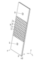
図6及び図7に例示される構成E1は、先に図1等を参照して説明したアンテナ装置1において、EBG素子10によって与えられる減衰特性を検討するための構成である。構成E1では、基板5Eの主面5Ea上に、間隔をあけて設けられた2つのアンテナ素子61E及びアンテナ素子62Eが設けられる。アンテナ素子61Eとアンテナ素子62Eとの間には、複数のEBG素子10Eが配置される。複数のEBG素子10Eは、複数のEBG素子11E及び複数のEBG素子12Eを含む。複数のEBG素子11E及び複数のEBG素子12Eは、それらの素子数及びそれらがアンテナ素子を囲んでいない点を除き、複数のEBG素子11及び複数のEBG素子12(図1)と同様に配置される。基板5Eの裏面5Eb上には、地板7Eが設けられる。
構成E1の具体的な構成について述べる。基板5Aの比誘電率は、2.97である。この比誘電率は、LCPを想定した値である。基板5Aの厚さは、0.1mmである。アンテナ素子61Eの形状及びアンテナ素子62Eの形状は、いずれも、1.042mm×1.042mmの四角形形状(共振周波数が約76GHz~77GHz)である。地板7E、EBG素子10E、EBG素子20E、アンテナ素子61E、アンテナ素子62E及び地板7Eを構成する金属パターンの導電率は、銅の導電率である。金属パターンの厚さは、0.043mmである。EBG素子11Eのパッチの形状は、1.031mm×1.031mmの四角形形状である。EBG素子12Eのパッチの形状は、半径が0.625の円形形状である。それらのパッチに設けられるビア(不図示)は、半径が0.05mmであり、パッチ中央に設けられる。
さらに図7に示される距離D1~D5も用いて述べると、隣り合うEBG素子11E及びEBG素子12Eの縁どうしの間の距離D1は、0.125mmである。アンテナ素子61Eから最も近いEBG素子11Eまでの距離D2は、2.714mmである。アンテナ素子62Eについても同様である。アンテナ素子61Eから最も近いEBG素子12Eまでの距離D3は、2.604mmである。アンテナ素子62Eについても同様である。アンテナ素子61Eから基板5Eの縁までの距離は、X軸方向における距離D4が5.479mmであり、Y軸方向における距離D5が4.479mmである。アンテナ素子62Eについても同様である。なお、次の図8~図10に示される構成については、構成E1と相違する部分を除き同様であり、相違する部分の構成は推測できるので、説明は省略する。
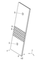
図8に例示される構成E2は、先に図5を参照して説明したアンテナ装置2において、EBG素子20によって与えられる減衰特性を検討するための構成である。構成E2は、構成E1と比較して、複数のEBG素子10E(図7)に代えて、複数のEBG素子20Eを含む。複数のEBG素子20Eは、複数のEBG素子21E及び複数のEBG素子22Eを含む。複数のEBG素子21E及び複数のEBG素子22Eは、それらの素子数及びそれらがアンテナ素子を囲んでいない点を除き、複数のEBG素子21及び複数のEBG素子22(図5)と同様に配置される。
図9に例示される構成E3は、比較例の構成である。構成E3は、構成E2と比較して、複数のEBG素子20Eに代えて、複数のEBG素子30Eを含む。複数のEBG素子30Eは、複数のEBG素子21E(図8)と同じであり、複数のEBG素子22Eに相当する構成は備えていない。
図10に例示される構成E4は、比較例の構成である。構成E4は、構成E2と比較して、複数のEBG素子20Eに代えて、複数のEBG素子40Eを含む。複数のEBG素子40は、複数のEBG素子22E(図8)と同じであり、複数のEBG素子21Eに相当する構成は備えていない。
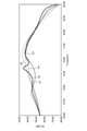
図11及び図12は、シミュレーション結果の例を示す図である。グラフの横軸は周波数を示し、グラフの縦軸はアンテナ素子61Eからアンテナ素子62EまでのS21(dB)を示す。周波数範囲は、65GHz~85GHzである。
図11に示されるグラフ線C0は、複数のEBG素子が存在しない場合のS21を示す。グラフ線C1~グラフ線C4は、構成E1~構成E4のS21を示す。図12に示されるグラフ線C1~C4は、複数のEBG素子が存在しない場合のS21を基準としたときの、構成E1~構成E4のS21の相対値を示す。
図11及び図12に示されるように、約76GHz~81GHzの周波数範囲では、構成E1~構成E4のいずれにおいても電磁波がある程度減衰する。約71GHz~86GHzの周波数範囲では、構成E2において減衰量が弱まる方向への変動が含まれるものの、構成E1及び構成E2のいずれにおいても、全体としての電磁波の減衰量は、構成E3及び構成E4における減衰量よりも大きい。すなわち、構成E1及び構成E2においては、構成E3及び構成E4よりも減衰帯域幅が広がるとともに減衰量も大きくなり、減衰特性が改善している。とくに構成E1における減衰量は、構成E2における減衰量よりもさらに大きく、構成E1における減衰特性は、構成E2における減衰特性よりもさらに改善している。
構成E1及び構成E2における減衰特性の改善は、アンテナ装置1及びアンテナ装置2における減衰特性の改善を示す。このことから、アンテナ装置1及びアンテナ装置2によって減衰特性が改善することが分かる。
以上説明した実施形態に係るアンテナ装置は、例えばレーダ装置に搭載されて用いられる。これについて、図13を参照して説明する。
図13は、レーダ装置の概略構成の例を示す図である。レーダ装置8は、送信部81と、アンテナ装置82と、アンテナ装置83と、受信部84と、制御部85とを含む。
送信部81は、送信処理を行う。送信処理は、変調処理、周波数変換処理(アップコンバート)、増幅処理、フィルタリング処理等を含みうる。変調の例はFM変調であるが、これ以外にもレーダに適したさまざまな変調が用いられてよい。
アンテナ装置82及びアンテナ装置83について説明する。アンテナ装置82は、送信信号を送信(放射)する。アンテナ装置83は、アンテナ装置82から送信された送信信号のうち、図示しないオブジェクトで反射した信号の一部を受信する。オブジェクトの例は、車両、人、建物等である。アンテナ装置82及びアンテナ装置83として、これまで説明したアンテナ装置1(図1)又はアンテナ装置2(図5)が用いられてよい。
受信部84は、受信処理を行う。受信処理は、増幅処理、フィルタリング処理、周波数変換処理(ダウンコンバート)、復調処理等を含みうる。
制御部85は、レーダ装置8の全体制御を行う。制御部85による制御は、送信部81による送信処理の制御、及び、受信部84による受信処理の制御を含む。これらの送信処理及び受信処理を制御することにより、制御部85は、例えばオブジェクトまでの距離を検出(測距)したり、オブジェクトの方位を検出(測位)したりする。このような測距及び/又は測位を行う機能ブロックとして、図13には、測距測位部85aが例示される。測距及び測位の手法自体は公知であるので、ここでは詳細な説明は省略する。
上述のレーダ装置8の構成は例示であり、適宜変更されてよい。例えば、アンテナ装置82及びアンテナ装置83が、送受信切替え可能に構成された一つのアンテナで構成されてもよい。
レーダ装置8によれば、バックローブ抑制効果が向上されているので、その分、例えば主ビームのエネルギーを大きくするなどして、より遠くのオブジェクトに対しても測距測位を行うことができるようになる。同じ距離に存在するオブジェクトに対しては、例えば測距測位精度が向上する。したがって、レーダ装置8の性能を向上させることができる。
2. 応用例
本開示に係る技術は、様々な製品へ応用することができる。例えば、本開示に係る技術は、自動車、電気自動車、ハイブリッド電気自動車、自動二輪車などのいずれかの種類の車両に搭載される装置として実現されてもよい。
本開示に係る技術は、様々な製品へ応用することができる。例えば、本開示に係る技術は、自動車、電気自動車、ハイブリッド電気自動車、自動二輪車などのいずれかの種類の車両に搭載される装置として実現されてもよい。
図14は、本開示に係る技術が適用され得る車両制御システム2000の概略的な構成の一例を示すブロック図である。車両制御システム2000は、通信ネットワーク2010を介して接続された複数の電子制御ユニットを備える。図14に示した例では、車両制御システム2000は、駆動系制御ユニット2100、ボディ系制御ユニット2200、バッテリ制御ユニット2300、車外情報検出装置2400、車内情報検出装置2500、及び統合制御ユニット2600を備える。これらの複数の制御ユニットを接続する通信ネットワーク2010は、例えば、CAN(Controller Area Network)、LIN(Local Interconnect Network)、LAN(Local Area Network)又はFlexRay(登録商標)等の任意の規格に準拠した車載通信ネットワークであってよい。
各制御ユニットは、各種プログラムにしたがって演算処理を行うマイクロコンピュータと、マイクロコンピュータにより実行されるプログラム又は各種演算に用いられるパラメータ等を記憶する記憶部と、各種制御対象の装置を駆動する駆動回路とを備える。各制御ユニットは、通信ネットワーク2010を介して他の制御ユニットとの間で通信を行うためのネットワークI/Fを備えるとともに、車内外の装置又はセンサ等との間で、有線通信又は無線通信により通信を行うための通信I/Fを備える。図13では、統合制御ユニット2600の機能構成として、マイクロコンピュータ2610、汎用通信I/F2620、専用通信I/F2630、測位部2640、ビーコン受信部2650、車内機器I/F2660、音声画像出力部2670、車載ネットワークI/F2680及び記憶部2690が図示されている。他の制御ユニットも同様に、マイクロコンピュータ、通信I/F及び記憶部等を備える。
駆動系制御ユニット2100は、各種プログラムにしたがって車両の駆動系に関連する装置の動作を制御する。例えば、駆動系制御ユニット2100は、内燃機関又は駆動用モータ等の車両の駆動力を発生させるための駆動力発生装置、駆動力を車輪に伝達するための駆動力伝達機構、車両の舵角を調節するステアリング機構、及び、車両の制動力を発生させる制動装置等の制御装置として機能する。駆動系制御ユニット2100は、ABS(Antilock Brake System)又はESC(Electronic Stability Control)等の制御装置としての機能を有してもよい。
駆動系制御ユニット2100には、車両状態検出部2110が接続される。車両状態検出部2110には、例えば、車体の軸回転運動の角速度を検出するジャイロセンサ、車両の加速度を検出する加速度センサ、あるいは、アクセルペダルの操作量、ブレーキペダルの操作量、ステアリングホイールの操舵角、エンジン回転数又は車輪の回転速度等を検出するためのセンサのうちの少なくとも一つが含まれる。駆動系制御ユニット2100は、車両状態検出部2110から入力される信号を用いて演算処理を行い、内燃機関、駆動用モータ、電動パワーステアリング装置又はブレーキ装置等を制御する。
ボディ系制御ユニット2200は、各種プログラムにしたがって車体に装備された各種装置の動作を制御する。例えば、ボディ系制御ユニット2200は、キーレスエントリシステム、スマートキーシステム、パワーウィンドウ装置、あるいは、ヘッドランプ、バックランプ、ブレーキランプ、ウィンカー又はフォグランプ等の各種ランプの制御装置として機能する。この場合、ボディ系制御ユニット2200には、鍵を代替する携帯機から発信される電波又は各種スイッチの信号が入力され得る。ボディ系制御ユニット2200は、これらの電波又は信号の入力を受け付け、車両のドアロック装置、パワーウィンドウ装置、ランプ等を制御する。
バッテリ制御ユニット2300は、各種プログラムにしたがって駆動用モータの電力供給源である二次電池2310を制御する。例えば、バッテリ制御ユニット2300には、二次電池2310を備えたバッテリ装置から、バッテリ温度、バッテリ出力電圧又はバッテリの残存容量等の情報が入力される。バッテリ制御ユニット2300は、これらの信号を用いて演算処理を行い、二次電池2310の温度調節制御又はバッテリ装置に備えられた冷却装置等の制御を行う。
車外情報検出装置2400は、車両制御システム2000を搭載した車両の外部の情報を検出する。例えば、車外情報検出装置2400には、撮像部2410及び車外情報検出部2420のうちの少なくとも一方が接続される。撮像部2410には、ToF(Time Of Flight)カメラ、ステレオカメラ、単眼カメラ、赤外線カメラ及びその他のカメラのうちの少なくとも一つが含まれる。車外情報検出部2420には、例えば、現在の天候又は気象を検出するための環境センサ、あるいは、車両制御システム2000を搭載した車両の周囲の他の車両、障害物又は歩行者等を検出するための周囲情報検出センサが含まれる。
環境センサは、例えば、雨天を検出する雨滴センサ、霧を検出する霧センサ、日照度合いを検出する日照センサ、及び降雪を検出する雪センサのうちの少なくとも一つであってよい。周囲情報検出センサは、超音波センサ、レーダ装置及びLIDAR(Light Detection and Ranging、Laser Imaging Detection and Ranging)装置のうちの少なくとも一つであってよい。これらの撮像部2410及び車外情報検出部2420は、それぞれ独立したセンサないし装置として備えられてもよいし、複数のセンサないし装置が統合された装置として備えられてもよい。
ここで、図15は、撮像部2410及び車外情報検出部2420の設置位置の例を示す。撮像部2910,2912,2914,2916,2918は、例えば、車両2900のフロントノーズ、サイドミラー、リアバンパ、バックドア及び車室内のフロントガラスの上部のうちの少なくとも一つの位置に設けられる。フロントノーズに備えられる撮像部2910及び車室内のフロントガラスの上部に備えられる撮像部2918は、主として車両2900の前方の画像を取得する。サイドミラーに備えられる撮像部2912,2914は、主として車両2900の側方の画像を取得する。リアバンパ又はバックドアに備えられる撮像部2916は、主として車両2900の後方の画像を取得する。車室内のフロントガラスの上部に備えられる撮像部2918は、主として先行車両又は、歩行者、障害物、信号機、交通標識又は車線等の検出に用いられる。
なお、図15には、それぞれの撮像部2910,2912,2914,2916の撮影範囲の一例が示されている。撮像範囲aは、フロントノーズに設けられた撮像部2910の撮像範囲を示し、撮像範囲b,cは、それぞれサイドミラーに設けられた撮像部2912,2914の撮像範囲を示し、撮像範囲dは、リアバンパ又はバックドアに設けられた撮像部2916の撮像範囲を示す。例えば、撮像部2910,2912,2914,2916で撮像された画像データが重ね合わせられることにより、車両2900を上方から見た俯瞰画像が得られる。
車両2900のフロント、リア、サイド、コーナ及び車室内のフロントガラスの上部に設けられる車外情報検出部2920,2922,2924,2926,2928,2930は、例えば超音波センサ又はレーダ装置であってよい。車両2900のフロントノーズ、リアバンパ、バックドア及び車室内のフロントガラスの上部に設けられる車外情報検出部2920,2926,2930は、例えばLIDAR装置であってよい。これらの車外情報検出部2920~2930は、主として先行車両、歩行者又は障害物等の検出に用いられる。
図14に戻って説明を続ける。車外情報検出装置2400は、撮像部2410に車外の画像を撮像させるとともに、撮像された画像データを受信する。また、車外情報検出装置2400は、接続されている車外情報検出部2420から検出情報を受信する。車外情報検出部2420が超音波センサ、レーダ装置又はLIDAR装置である場合には、車外情報検出装置2400は、超音波又は電磁波等を発信させるとともに、受信された反射波の情報を受信する。車外情報検出装置2400は、受信した情報に基づいて、人、車、障害物、標識又は路面上の文字等の物体検出処理又は距離検出処理を行ってもよい。車外情報検出装置2400は、受信した情報に基づいて、降雨、霧又は路面状況等を認識する環境認識処理を行ってもよい。車外情報検出装置2400は、受信した情報に基づいて、車外の物体までの距離を算出してもよい。
また、車外情報検出装置2400は、受信した画像データに基づいて、人、車、障害物、標識又は路面上の文字等を認識する画像認識処理又は距離検出処理を行ってもよい。車外情報検出装置2400は、受信した画像データに対して歪補正又は位置合わせ等の処理を行うとともに、異なる撮像部2410により撮像された画像データを合成して、俯瞰画像又はパノラマ画像を生成してもよい。車外情報検出装置2400は、異なる撮像部2410により撮像された画像データを用いて、視点変換処理を行ってもよい。
車内情報検出装置2500は、車内の情報を検出する。車内情報検出装置2500には、例えば、運転者の状態を検出する運転者状態検出部2510が接続される。運転者状態検出部2510は、運転者を撮像するカメラ、運転者の生体情報を検出する生体センサ又は車室内の音声を集音するマイク等を含んでもよい。生体センサは、例えば、座面又はステアリングホイール等に設けられ、座席に座った搭乗者又はステアリングホイールを握る運転者の生体情報を検出する。車内情報検出装置2500は、運転者状態検出部2510から入力される検出情報に基づいて、運転者の疲労度合い又は集中度合いを算出してもよいし、運転者が居眠りをしていないかを判別してもよい。車内情報検出装置2500は、集音された音声信号に対してノイズキャンセリング処理等の処理を行ってもよい。
統合制御ユニット2600は、各種プログラムにしたがって車両制御システム2000内の動作全般を制御する。統合制御ユニット2600には、入力部2800が接続されている。入力部2800は、例えば、タッチパネル、ボタン、マイクロフォン、スイッチ又はレバー等、搭乗者によって入力操作され得る装置によって実現される。入力部2800は、例えば、赤外線又はその他の電波を利用したリモートコントロール装置であってもよいし、車両制御システム2000の操作に対応した携帯電話又はPDA(Personal Digital Assistant)等の外部接続機器であってもよい。入力部2800は、例えばカメラであってもよく、その場合搭乗者はジェスチャにより情報を入力することができる。さらに、入力部2800は、例えば、上記の入力部2800を用いて搭乗者等により入力された情報に基づいて入力信号を生成し、統合制御ユニット2600に出力する入力制御回路などを含んでもよい。搭乗者等は、この入力部2800を操作することにより、車両制御システム2000に対して各種のデータを入力したり処理動作を指示したりする。
記憶部2690は、マイクロコンピュータにより実行される各種プログラムを記憶するRAM(Random Access Memory)、及び各種パラメータ、演算結果又はセンサ値等を記憶するROM(Read Only Memory)を含んでいてもよい。また、記憶部2690は、HDD(Hard Disc Drive)等の磁気記憶デバイス、半導体記憶デバイス、光記憶デバイス又は光磁気記憶デバイス等によって実現してもよい。
汎用通信I/F2620は、外部環境2750に存在する様々な機器との間の通信を仲介する汎用的な通信I/Fである。汎用通信I/F2620は、GSM(Global System of Mobile communications)(登録商標)、WiMAX、LTE(Long Term Evolution)若しくはLTE-A(LTE-Advanced)などのセルラー通信プロトコル、又は無線LAN(Wi-Fi(登録商標)ともいう)などのその他の無線通信プロトコルを実装してよい。汎用通信I/F2620は、例えば、基地局又はアクセスポイントを介して、外部ネットワーク(例えば、インターネット、クラウドネットワーク又は事業者固有のネットワーク)上に存在する機器(例えば、アプリケーションサーバ又は制御サーバ)へ接続してもよい。また、汎用通信I/F2620は、例えばP2P(Peer To Peer)技術を用いて、車両の近傍に存在する端末(例えば、歩行者若しくは店舗の端末、又はMTC(Machine Type Communication)端末)と接続してもよい。
専用通信I/F2630は、車両における使用を目的として策定された通信プロトコルをサポートする通信I/Fである。専用通信I/F2630は、例えば、下位レイヤのIEEE802.11pと上位レイヤのIEEE1609との組合せであるWAVE(Wireless Access in Vehicle Environment)、又はDSRC(Dedicated Short Range Communications)といった標準プロトコルを実装してよい。専用通信I/F2630は、典型的には、車車間(Vehicle to Vehicle)通信、路車間(Vehicle to Infrastructure)通信及び歩車間(Vehicle to Pedestrian)通信のうちの1つ以上を含む概念であるV2X通信を遂行する。
測位部2640は、例えば、GNSS(Global Navigation Satellite System)衛星からのGNSS信号(例えば、GPS(Global Positioning System)衛星からのGPS信号)を受信して測位を実行し、車両の緯度、経度及び高度を含む位置情報を生成する。なお、測位部2640は、無線アクセスポイントとの信号の交換により現在位置を特定してもよく、又は測位機能を有する携帯電話、PHS若しくはスマートフォンといった端末から位置情報を取得してもよい。
ビーコン受信部2650は、例えば、道路上に設置された無線局等から発信される電波あるいは電磁波を受信し、現在位置、渋滞、通行止め又は所要時間等の情報を取得する。なお、ビーコン受信部2650の機能は、上述した専用通信I/F2630に含まれてもよい。
車内機器I/F2660は、マイクロコンピュータ2610と車内に存在する様々な機器との間の接続を仲介する通信インタフェースである。車内機器I/F2660は、無線LAN、Bluetooth(登録商標)、NFC(Near Field Communication)又はWUSB(Wireless USB)といった無線通信プロトコルを用いて無線接続を確立してもよい。また、車内機器I/F2660は、図示しない接続端子(及び、必要であればケーブル)を介して有線接続を確立してもよい。車内機器I/F2660は、例えば、搭乗者が有するモバイル機器若しくはウェアラブル機器、又は車両に搬入され若しくは取り付けられる情報機器との間で、制御信号又はデータ信号を交換する。
車載ネットワークI/F2680は、マイクロコンピュータ2610と通信ネットワーク2010との間の通信を仲介するインタフェースである。車載ネットワークI/F2680は、通信ネットワーク2010によりサポートされる所定のプロトコルに則して、信号等を送受信する。
統合制御ユニット2600のマイクロコンピュータ2610は、汎用通信I/F2620、専用通信I/F2630、測位部2640、ビーコン受信部2650、車内機器I/F2660及び車載ネットワークI/F2680のうちの少なくとも一つを介して取得される情報に基づき、各種プログラムにしたがって、車両制御システム2000を制御する。例えば、マイクロコンピュータ2610は、取得される車内外の情報に基づいて、駆動力発生装置、ステアリング機構又は制動装置の制御目標値を演算し、駆動系制御ユニット2100に対して制御指令を出力してもよい。例えば、マイクロコンピュータ2610は、車両の衝突回避あるいは衝撃緩和、車間距離に基づく追従走行、車速維持走行、自動運転等を目的とした協調制御を行ってもよい。
マイクロコンピュータ2610は、汎用通信I/F2620、専用通信I/F2630、測位部2640、ビーコン受信部2650、車内機器I/F2660及び車載ネットワークI/F2680のうちの少なくとも一つを介して取得される情報に基づき、車両の現在位置の周辺情報を含むローカル地図情報を作成してもよい。また、マイクロコンピュータ2610は、取得される情報に基づき、車両の衝突、歩行者等の近接又は通行止めの道路への進入等の危険を予測し、警告用信号を生成してもよい。警告用信号は、例えば、警告音を発生させたり、警告ランプを点灯させたりするための信号であってよい。
音声画像出力部2670は、車両の搭乗者又は車外に対して、視覚的又は聴覚的に情報を通知することが可能な出力装置へ音声及び画像のうちの少なくとも一方の出力信号を送信する。図14の例では、出力装置として、オーディオスピーカ2710、表示部2720及びインストルメントパネル2730が例示されている。表示部2720は、例えば、オンボードディスプレイ及びヘッドアップディスプレイの少なくとも一つを含んでいてもよい。表示部2720は、AR(Augmented Reality)表示機能を有していてもよい。出力装置は、これらの装置以外の、ヘッドホン、プロジェクタ又はランプ等の他の装置であってもよい。出力装置が表示装置の場合、表示装置は、マイクロコンピュータ2610が行った各種処理により得られた結果又は他の制御ユニットから受信された情報を、テキスト、イメージ、表、グラフ等、様々な形式で視覚的に表示する。また、出力装置が音声出力装置の場合、音声出力装置は、再生された音声データ又は音響データ等からなるオーディオ信号をアナログ信号に変換して聴覚的に出力する。
なお、図14に示した例において、通信ネットワーク2010を介して接続された少なくとも二つの制御ユニットが一つの制御ユニットとして一体化されてもよい。あるいは、個々の制御ユニットが、複数の制御ユニットにより構成されてもよい。さらに、車両制御システム2000が、図示されていない別の制御ユニットを備えてもよい。また、上記の説明において、いずれかの制御ユニットが担う機能の一部又は全部を、他の制御ユニットに持たせてもよい。つまり、通信ネットワーク2010を介して情報の送受信がされるようになっていれば、所定の演算処理が、いずれかの制御ユニットで行われるようになってもよい。同様に、いずれかの制御ユニットに接続されているセンサ又は装置が、他の制御ユニットに接続されるとともに、複数の制御ユニットが、通信ネットワーク2010を介して相互に検出情報を送受信してもよい。
以上説明した車両制御システム2000において、図1及び図5等を用いて説明した本実施形態に係るアンテナ装置1及びアンテナ装置2、さらには図13等を用いて説明した本実施形態に係るレーダ装置8は、図14に示した応用例の車外情報検出部2420に適用することができる。すなわち、バックローブ抑制効果が向上されたアンテナ装置1、アンテナ装置2又はレーダ装置8を用いることで、例えば検出性能を向上させることができる。
3. 効果
以上説明した実施形態に係るアンテナ装置は、例えば次のように特定される。図1等を参照して説明したように、アンテナ装置1は、アンテナ素子6と、複数のEBG素子10と、を備える。複数のEBG素子10は、複数のEBG素子11と、複数のEBG素子11とは異なる構造を有する複数のEBG素子12とを含む。
以上説明した実施形態に係るアンテナ装置は、例えば次のように特定される。図1等を参照して説明したように、アンテナ装置1は、アンテナ素子6と、複数のEBG素子10と、を備える。複数のEBG素子10は、複数のEBG素子11と、複数のEBG素子11とは異なる構造を有する複数のEBG素子12とを含む。
上記のアンテナ装置1によれば、複数のEBG素子12が複数のEBG素子11とは異なる構造を有するので、複数のEBG素子12によって与えられる減衰特性は、複数のEBG素子11によって与える減衰特性とは異なる。したがって、異なる2つの減衰特性を併せ持った減衰特性が得られる。例えば、一つの減衰特性しか与えられない場合と比較して、より広い減衰帯域幅が得られたり、より大きな減衰量が得られたりする等、減衰特性が改善する。減衰特性の改善により、例えばバックローブの抑制効果を向上させることができる。
図1等を参照して説明したように、複数のEBG素子10は、アンテナ素子6を囲んでいてよい。これにより、アンテナ素子6及びEBG素子10を含む平面(例えばXY平面)において、アンテナ素子6からその平面方向に向かって進む電磁波を減衰させることができる。
図1等を参照して説明したように、複数のEBG素子11の各々と、複数のEBG素子12の各々とが、交互に配置されていてよい。例えばこのようにして、互いに異なる構造を有する複数のEBG素子11及び複数のEBG素子12を配置することができる。図5等を参照して説明したように、複数のEBG素子21は、アンテナ素子6を囲んでおり、複数のEBG素子22は、EBG素子21を囲んでいてよい。このようにして、互いに異なる構造を有する複数のEBG素子21及び複数のEBG素子22を配置することもできる。
図1等を参照して説明したように、アンテナ素子6及び複数のEBG素子10は、基板5の主面5a上に配置されてよい。これにより、アンテナ装置1を平面アンテナとして用いることができる。アンテナ装置1をコンパクトにできる等のメリットがある。
図1等を参照して説明したように、複数のEBG素子11は、アンテナ素子6から離間して設けられ、複数のEBG素子10とアンテナ素子6との離間距離は、隣り合うEBG素子11どうしの離間距離より大きくてよい。これにより、主ビームにある程度の幅を持たせることができる。
図1等を参照して説明したように、複数のEBG素子11が設けられる領域は、基板5の縁部を含んでよい。これにより、複数のEBG素子10の配置面積が確保しやすくなる。
図3及び図4等を参照して説明したように、複数のEBG素子10の各々は、基板5の主面5a上に設けられたパッチ10aと、基板5の裏面5b上に設けられた地板7及びパッチ10aを接続するビア10bと、を含んでよい。例えばこのようなマッシュルーム構造を用いることで、複数のEBG素子10を平面アンテナに組み入れることができる。
複数のEBG素子10の構造を規定するパラメータは、パッチ10aのサイズ、ビア10bのサイズ、及び、隣り合うEBG素子10のパッチ10aどうしの間の間隔の少なくとも一つを含み、複数のEBG素子12の構造を規定するパラメータは、複数のEBG素子11の構造を規定するパラメータと異なっていてよい。例えばこのようにして、複数のEBG素子12に、複数のEBG素子11とは異なる構造を持たせることができる。
図13等を参照して説明したように、アンテナ装置82及びアンテナ装置83は、レーダ装置8に搭載されてよい。これにより、レーダ装置8の性能を向上させることができる。
図14及び図15等を参照して説明したように、アンテナ装置は、車両に搭載されてよい。これにより、車外情報検出部の検出性能を向上させることができる。
最後に、アンテナ装置(図1)のシミュレーション結果の一例について、図16及び図17を参照して説明する。図16及び図17は、シミュレーション結果の例を示す図である。図16は、周波数76GHzにおける指向性のシミュレーション結果を示す。グラフの上側は基板5の主面5a側(Z軸正方向側)の指向性を示し、グラフの下側は基板5の裏面5b側(Z軸負方向側)の指向性を示す。グラフ線G0は、アンテナ装置1(図1)において複数のEBG素子10が存在しない構成の指向性を示す。グラフ線G1は、アンテナ装置1のように複数のEBG素子11及び複数のEBG素子12が混在する構成の指向性を示す。グラフ線G2は、アンテナ装置1において複数のEBG素子10がいずれも複数のEBG素子11である構成の指向性を示す。
図17のグラフの横軸は周波数を示し、グラフの縦軸は裏面放射量(dB)を示す。グラフの横軸は周波数を示し、グラフの縦軸はアンテナ装置1において複数のEBG素子10が存在しない構成の放射量を基準としたときの裏面放射量(dB)を示す。
図16及び図17に示されるように、EBG素子が存在しない場合(グラフ線G0)と比較して、EBG素子が存在する場合(グラフ線G1及びグラフ線G2)の方が、基板5の裏面5b側への放射量が少なくなっていることがわかる。また、同じ構造の複数のEBG素子11だけを備える構成(グラフ線G2)に比べて、異なる構造の複数のEBG素子11及び複数のEBG素子12を備える構成(グラフ線G1)の方が、放射量が少なくなる帯域が広帯域化されていることが分かる(この例では74GHz付近)。
なお、本開示に記載された効果は、あくまで例示であって、開示された内容に限定されない。他の効果があってもよい。
以上、本開示の実施形態について説明したが、本開示の技術的範囲は、上述の実施形態そのままに限定されるものではなく、本開示の要旨を逸脱しない範囲において種々の変更が可能である。また、異なる実施形態及び変形例にわたる構成要素を適宜組み合わせてもよい。
また、本明細書に記載された各実施形態における効果はあくまで例示であって限定されるものでは無く、他の効果があってもよい。
上記実施形態では、複数のEBG素子が、互いに異なる構造を有する2種類の複数のEBG素子を備える例について説明した。ただし、複数のEBG素子は、それぞれが異なる構造を有する3種類以上の複数のEBG素子を備えていてもよい。
なお、本技術は以下のような構成も取ることができる。
(1)
アンテナ素子と、
複数のEBG素子と、
を備え、
前記複数のEBG素子は、
複数の第1のEBG素子と、
前記複数の第1のEBG素子は異なる構造を有する複数の第2のEBG素子と、
を含む、
アンテナ装置。
(2)
前記複数のEBG素子は、前記アンテナ素子を囲んでいる、
(1)に記載のアンテナ装置。
(3)
前記複数の第1のEBG素子の各々と、前記複数の第2のEBG素子の各々とが、交互に配置されている、
(1)又は(2)に記載のアンテナ装置。
(4)
前記複数の第1のEBG素子は、前記アンテナ素子を囲んでおり、
前記複数の第2のEBG素子は、前記複数の第1のEBG素子を囲んでいる、
(1)又は(2)に記載のアンテナ装置。
(5)
前記アンテナ素子及び前記複数のEBG素子は、基板の主面上に配置される、
(1)~(4)のいずれかに記載のアンテナ装置。
(6)
前記複数のEBG素子は、前記アンテナ素子から離間して設けられ、
前記複数のEBG素子と前記アンテナ素子との離間距離は、前記複数のEBG素子のうちの隣り合うEBG素子どうしの離間距離よりも大きい、
(5)に記載のアンテナ装置。
(7)
前記複数のEBG素子が設けられる領域は、前記基板の縁部を含む、
(5)又は(6)に記載のアンテナ装置。
(8)
前記複数のEBG素子の各々は、
前記基板の前記主面上に設けられたパッチと、
前記基板の裏面上に設けられた地板及び前記パッチを接続するビアと、
を含む、
(5)~(7)のいずれかに記載のアンテナ装置。
(9)
前記複数のEBG素子の構造を規定するパラメータは、前記パッチのサイズ、前記ビアのサイズ、及び、隣り合う前記EBG素子の前記パッチどうしの間の間隔の少なくとも一つを含み、
前記複数の第2のEBG素子の構造を規定する前記パラメータは、前記複数の第1のEBG素子を規定する前記パラメータとは異なる、
(8)に記載のアンテナ装置。
(10)
レーダ装置に搭載される、(1)~(7)のいずれかに記載のアンテナ装置。
(11)
車両に搭載される、(1)~(8)のいずれかに記載のアンテナ装置。
(1)
アンテナ素子と、
複数のEBG素子と、
を備え、
前記複数のEBG素子は、
複数の第1のEBG素子と、
前記複数の第1のEBG素子は異なる構造を有する複数の第2のEBG素子と、
を含む、
アンテナ装置。
(2)
前記複数のEBG素子は、前記アンテナ素子を囲んでいる、
(1)に記載のアンテナ装置。
(3)
前記複数の第1のEBG素子の各々と、前記複数の第2のEBG素子の各々とが、交互に配置されている、
(1)又は(2)に記載のアンテナ装置。
(4)
前記複数の第1のEBG素子は、前記アンテナ素子を囲んでおり、
前記複数の第2のEBG素子は、前記複数の第1のEBG素子を囲んでいる、
(1)又は(2)に記載のアンテナ装置。
(5)
前記アンテナ素子及び前記複数のEBG素子は、基板の主面上に配置される、
(1)~(4)のいずれかに記載のアンテナ装置。
(6)
前記複数のEBG素子は、前記アンテナ素子から離間して設けられ、
前記複数のEBG素子と前記アンテナ素子との離間距離は、前記複数のEBG素子のうちの隣り合うEBG素子どうしの離間距離よりも大きい、
(5)に記載のアンテナ装置。
(7)
前記複数のEBG素子が設けられる領域は、前記基板の縁部を含む、
(5)又は(6)に記載のアンテナ装置。
(8)
前記複数のEBG素子の各々は、
前記基板の前記主面上に設けられたパッチと、
前記基板の裏面上に設けられた地板及び前記パッチを接続するビアと、
を含む、
(5)~(7)のいずれかに記載のアンテナ装置。
(9)
前記複数のEBG素子の構造を規定するパラメータは、前記パッチのサイズ、前記ビアのサイズ、及び、隣り合う前記EBG素子の前記パッチどうしの間の間隔の少なくとも一つを含み、
前記複数の第2のEBG素子の構造を規定する前記パラメータは、前記複数の第1のEBG素子を規定する前記パラメータとは異なる、
(8)に記載のアンテナ装置。
(10)
レーダ装置に搭載される、(1)~(7)のいずれかに記載のアンテナ装置。
(11)
車両に搭載される、(1)~(8)のいずれかに記載のアンテナ装置。
1 アンテナ装置
2 アンテナ装置
5 基板
6 アンテナ素子
7 地板
8 レーダ装置
10 EBG素子
11 EBG素子
12 EBG素子
20 EBG素子
21 EBG素子
22 EBG素子
81 送信部
82 アンテナ装置
83 アンテナ装置
84 受信部
85 制御部
85a 測距測位部
2 アンテナ装置
5 基板
6 アンテナ素子
7 地板
8 レーダ装置
10 EBG素子
11 EBG素子
12 EBG素子
20 EBG素子
21 EBG素子
22 EBG素子
81 送信部
82 アンテナ装置
83 アンテナ装置
84 受信部
85 制御部
85a 測距測位部
Claims (11)
- アンテナ素子と、
複数のEBG素子と、
を備え、
前記複数のEBG素子は、
複数の第1のEBG素子と、
前記複数の第1のEBG素子は異なる構造を有する複数の第2のEBG素子と、
を含む、
アンテナ装置。 - 前記複数のEBG素子は、前記アンテナ素子を囲んでいる、
請求項1に記載のアンテナ装置。 - 前記複数の第1のEBG素子の各々と、前記複数の第2のEBG素子の各々とが、交互に配置されている、
請求項1に記載のアンテナ装置。 - 前記複数の第1のEBG素子は、前記アンテナ素子を囲んでおり、
前記複数の第2のEBG素子は、前記複数の第1のEBG素子を囲んでいる、
請求項1に記載のアンテナ装置。 - 前記アンテナ素子及び前記複数のEBG素子は、基板の主面上に配置される、
請求項1に記載のアンテナ装置。 - 前記複数のEBG素子は、前記アンテナ素子から離間して設けられ、
前記複数のEBG素子と前記アンテナ素子との離間距離は、前記複数のEBG素子のうちの隣り合うEBG素子どうしの離間距離よりも大きい、
請求項5に記載のアンテナ装置。 - 前記複数のEBG素子が設けられる領域は、前記基板の縁部を含む、
請求項5に記載のアンテナ装置。 - 前記複数のEBG素子の各々は、
前記基板の前記主面上に設けられたパッチと、
前記基板の裏面上に設けられた地板及び前記パッチを接続するビアと、
を含む、
請求項5に記載のアンテナ装置。 - 前記複数のEBG素子の構造を規定するパラメータは、前記パッチのサイズ、前記ビアのサイズ、及び、隣り合う前記EBG素子の前記パッチどうしの間の間隔の少なくとも一つを含み、
前記複数の第2のEBG素子の構造を規定する前記パラメータは、前記複数の第1のEBG素子を規定する前記パラメータとは異なる、
請求項8に記載のアンテナ装置。 - レーダ装置に搭載される、請求項1に記載のアンテナ装置。
- 車両に搭載される、請求項1に記載のアンテナ装置。
Priority Applications (1)
| Application Number | Priority Date | Filing Date | Title |
|---|---|---|---|
| US18/009,540 US12431629B2 (en) | 2020-07-21 | 2021-07-09 | Antenna device including different electromagnetic band gap (EBG) elements |
Applications Claiming Priority (2)
| Application Number | Priority Date | Filing Date | Title |
|---|---|---|---|
| JP2020-124390 | 2020-07-21 | ||
| JP2020124390 | 2020-07-21 |
Publications (1)
| Publication Number | Publication Date |
|---|---|
| WO2022019148A1 true WO2022019148A1 (ja) | 2022-01-27 |
Family
ID=79728774
Family Applications (1)
| Application Number | Title | Priority Date | Filing Date |
|---|---|---|---|
| PCT/JP2021/025926 Ceased WO2022019148A1 (ja) | 2020-07-21 | 2021-07-09 | アンテナ装置 |
Country Status (2)
| Country | Link |
|---|---|
| US (1) | US12431629B2 (ja) |
| WO (1) | WO2022019148A1 (ja) |
Families Citing this family (2)
| Publication number | Priority date | Publication date | Assignee | Title |
|---|---|---|---|---|
| WO2022019148A1 (ja) * | 2020-07-21 | 2022-01-27 | ソニーセミコンダクタソリューションズ株式会社 | アンテナ装置 |
| JP7775897B2 (ja) * | 2022-01-06 | 2025-11-26 | 株式会社オートネットワーク技術研究所 | アンテナモジュール及び車両 |
Citations (5)
| Publication number | Priority date | Publication date | Assignee | Title |
|---|---|---|---|---|
| WO2008050441A1 (fr) * | 2006-10-26 | 2008-05-02 | Panasonic Corporation | Dispositif d'antenne |
| JP2010199881A (ja) * | 2009-02-24 | 2010-09-09 | Nec Corp | 導波路構造、プリント配線板、アンテナ、アレイアンテナ及びプリント基板並びにそれを用いた電子装置 |
| WO2013001692A1 (ja) * | 2011-06-28 | 2013-01-03 | 日本電気株式会社 | 電子装置及びノイズ抑制方法 |
| JP2016039541A (ja) * | 2014-08-08 | 2016-03-22 | 株式会社日本自動車部品総合研究所 | 表面電流抑制フィルタ及びアンテナ装置 |
| JP2018129623A (ja) * | 2017-02-07 | 2018-08-16 | パナソニック株式会社 | モジュール、無線通信装置、および、レーダ装置 |
Family Cites Families (5)
| Publication number | Priority date | Publication date | Assignee | Title |
|---|---|---|---|---|
| US7760140B2 (en) * | 2006-06-09 | 2010-07-20 | Intel Corporation | Multiband antenna array using electromagnetic bandgap structures |
| WO2019066176A1 (ko) * | 2017-09-27 | 2019-04-04 | 엘지전자 주식회사 | 전자 장치 |
| KR102667512B1 (ko) * | 2019-11-15 | 2024-05-22 | 엘지전자 주식회사 | 5g 안테나를 구비하는 전자 기기 |
| SE2030028A1 (en) * | 2020-01-31 | 2021-01-12 | Gapwaves Ab | A scalable modular antenna arrangement |
| WO2022019148A1 (ja) * | 2020-07-21 | 2022-01-27 | ソニーセミコンダクタソリューションズ株式会社 | アンテナ装置 |
-
2021
- 2021-07-09 WO PCT/JP2021/025926 patent/WO2022019148A1/ja not_active Ceased
- 2021-07-09 US US18/009,540 patent/US12431629B2/en active Active
Patent Citations (5)
| Publication number | Priority date | Publication date | Assignee | Title |
|---|---|---|---|---|
| WO2008050441A1 (fr) * | 2006-10-26 | 2008-05-02 | Panasonic Corporation | Dispositif d'antenne |
| JP2010199881A (ja) * | 2009-02-24 | 2010-09-09 | Nec Corp | 導波路構造、プリント配線板、アンテナ、アレイアンテナ及びプリント基板並びにそれを用いた電子装置 |
| WO2013001692A1 (ja) * | 2011-06-28 | 2013-01-03 | 日本電気株式会社 | 電子装置及びノイズ抑制方法 |
| JP2016039541A (ja) * | 2014-08-08 | 2016-03-22 | 株式会社日本自動車部品総合研究所 | 表面電流抑制フィルタ及びアンテナ装置 |
| JP2018129623A (ja) * | 2017-02-07 | 2018-08-16 | パナソニック株式会社 | モジュール、無線通信装置、および、レーダ装置 |
Also Published As
| Publication number | Publication date |
|---|---|
| US12431629B2 (en) | 2025-09-30 |
| US20230238708A1 (en) | 2023-07-27 |
Similar Documents
| Publication | Publication Date | Title |
|---|---|---|
| US11076141B2 (en) | Image processing device, image processing method, and vehicle | |
| WO2020100569A1 (ja) | 制御装置、制御方法及びセンサ制御システム | |
| JP6764573B2 (ja) | 画像処理装置、画像処理方法、およびプログラム | |
| WO2017057043A1 (ja) | 画像処理装置、画像処理方法、およびプログラム | |
| US11909122B2 (en) | Moving object mounted radar antenna, module for moving object mounted radar antenna, and moving object mounted radar antenna system | |
| KR102824506B1 (ko) | 안테나 및 차량 | |
| US12431629B2 (en) | Antenna device including different electromagnetic band gap (EBG) elements | |
| WO2021106558A1 (ja) | レーダー装置、レーダー装置の製造方法及び送受信機 | |
| CN113557634B (zh) | 定向耦合器、无线电通信装置和控制方法 | |
| CN111868778B (zh) | 图像处理装置、图像处理方法以及存储介质 | |
| WO2022075062A1 (ja) | 物体位置検出装置、物体位置検出システム及び物体位置検出方法 | |
| JPWO2018159304A1 (ja) | 送信装置および通信システム | |
| KR20260040015A (ko) | 전자 기기 및 레이다 장치 | |
| WO2018051621A1 (ja) | 通信装置、および通信システム | |
| WO2022044830A1 (ja) | 情報処理装置、および情報処理方法 | |
| WO2025173450A1 (ja) | アンテナ装置及びレーダ装置 | |
| US10958359B2 (en) | Communication apparatus and communication system | |
| WO2024048671A1 (ja) | レーダ装置および車載センシングシステム | |
| WO2025013644A1 (ja) | 情報処理装置、レーダ装置及び情報処理方法 | |
| JP2022181125A (ja) | 情報処理装置、キャリブレーションシステム及び情報処理方法 | |
| WO2020255589A1 (ja) | 情報処理装置、情報処理方法及びプログラム |
Legal Events
| Date | Code | Title | Description |
|---|---|---|---|
| 121 | Ep: the epo has been informed by wipo that ep was designated in this application |
Ref document number: 21846071 Country of ref document: EP Kind code of ref document: A1 |
|
| NENP | Non-entry into the national phase |
Ref country code: DE |
|
| 122 | Ep: pct application non-entry in european phase |
Ref document number: 21846071 Country of ref document: EP Kind code of ref document: A1 |
|
| NENP | Non-entry into the national phase |
Ref country code: JP |
|
| WWG | Wipo information: grant in national office |
Ref document number: 18009540 Country of ref document: US |