WO2022019089A1 - Power module - Google Patents
Power module Download PDFInfo
- Publication number
- WO2022019089A1 WO2022019089A1 PCT/JP2021/025107 JP2021025107W WO2022019089A1 WO 2022019089 A1 WO2022019089 A1 WO 2022019089A1 JP 2021025107 W JP2021025107 W JP 2021025107W WO 2022019089 A1 WO2022019089 A1 WO 2022019089A1
- Authority
- WO
- WIPO (PCT)
- Prior art keywords
- heat dissipation
- power module
- power semiconductor
- circuit board
- thermal resistance
- Prior art date
Links
Images


Classifications
-
- H—ELECTRICITY
- H01—ELECTRIC ELEMENTS
- H01L—SEMICONDUCTOR DEVICES NOT COVERED BY CLASS H10
- H01L23/00—Details of semiconductor or other solid state devices
- H01L23/34—Arrangements for cooling, heating, ventilating or temperature compensation ; Temperature sensing arrangements
- H01L23/36—Selection of materials, or shaping, to facilitate cooling or heating, e.g. heatsinks
- H01L23/373—Cooling facilitated by selection of materials for the device or materials for thermal expansion adaptation, e.g. carbon
- H01L23/3735—Laminates or multilayers, e.g. direct bond copper ceramic substrates
-
- H—ELECTRICITY
- H01—ELECTRIC ELEMENTS
- H01L—SEMICONDUCTOR DEVICES NOT COVERED BY CLASS H10
- H01L23/00—Details of semiconductor or other solid state devices
- H01L23/02—Containers; Seals
- H01L23/04—Containers; Seals characterised by the shape of the container or parts, e.g. caps, walls
-
- H—ELECTRICITY
- H01—ELECTRIC ELEMENTS
- H01L—SEMICONDUCTOR DEVICES NOT COVERED BY CLASS H10
- H01L23/00—Details of semiconductor or other solid state devices
- H01L23/34—Arrangements for cooling, heating, ventilating or temperature compensation ; Temperature sensing arrangements
- H01L23/36—Selection of materials, or shaping, to facilitate cooling or heating, e.g. heatsinks
- H01L23/367—Cooling facilitated by shape of device
- H01L23/3677—Wire-like or pin-like cooling fins or heat sinks
-
- H—ELECTRICITY
- H01—ELECTRIC ELEMENTS
- H01L—SEMICONDUCTOR DEVICES NOT COVERED BY CLASS H10
- H01L23/00—Details of semiconductor or other solid state devices
- H01L23/34—Arrangements for cooling, heating, ventilating or temperature compensation ; Temperature sensing arrangements
- H01L23/42—Fillings or auxiliary members in containers or encapsulations selected or arranged to facilitate heating or cooling
- H01L23/433—Auxiliary members in containers characterised by their shape, e.g. pistons
- H01L23/4334—Auxiliary members in encapsulations
-
- H—ELECTRICITY
- H01—ELECTRIC ELEMENTS
- H01L—SEMICONDUCTOR DEVICES NOT COVERED BY CLASS H10
- H01L23/00—Details of semiconductor or other solid state devices
- H01L23/52—Arrangements for conducting electric current within the device in operation from one component to another, i.e. interconnections, e.g. wires, lead frames
- H01L23/522—Arrangements for conducting electric current within the device in operation from one component to another, i.e. interconnections, e.g. wires, lead frames including external interconnections consisting of a multilayer structure of conductive and insulating layers inseparably formed on the semiconductor body
- H01L23/532—Arrangements for conducting electric current within the device in operation from one component to another, i.e. interconnections, e.g. wires, lead frames including external interconnections consisting of a multilayer structure of conductive and insulating layers inseparably formed on the semiconductor body characterised by the materials
- H01L23/53204—Conductive materials
- H01L23/5328—Conductive materials containing conductive organic materials or pastes, e.g. conductive adhesives, inks
-
- H—ELECTRICITY
- H01—ELECTRIC ELEMENTS
- H01L—SEMICONDUCTOR DEVICES NOT COVERED BY CLASS H10
- H01L25/00—Assemblies consisting of a plurality of individual semiconductor or other solid state devices ; Multistep manufacturing processes thereof
- H01L25/03—Assemblies consisting of a plurality of individual semiconductor or other solid state devices ; Multistep manufacturing processes thereof all the devices being of a type provided for in the same subgroup of groups H01L27/00 - H01L33/00, or in a single subclass of H10K, H10N, e.g. assemblies of rectifier diodes
- H01L25/04—Assemblies consisting of a plurality of individual semiconductor or other solid state devices ; Multistep manufacturing processes thereof all the devices being of a type provided for in the same subgroup of groups H01L27/00 - H01L33/00, or in a single subclass of H10K, H10N, e.g. assemblies of rectifier diodes the devices not having separate containers
- H01L25/07—Assemblies consisting of a plurality of individual semiconductor or other solid state devices ; Multistep manufacturing processes thereof all the devices being of a type provided for in the same subgroup of groups H01L27/00 - H01L33/00, or in a single subclass of H10K, H10N, e.g. assemblies of rectifier diodes the devices not having separate containers the devices being of a type provided for in group H01L29/00
- H01L25/072—Assemblies consisting of a plurality of individual semiconductor or other solid state devices ; Multistep manufacturing processes thereof all the devices being of a type provided for in the same subgroup of groups H01L27/00 - H01L33/00, or in a single subclass of H10K, H10N, e.g. assemblies of rectifier diodes the devices not having separate containers the devices being of a type provided for in group H01L29/00 the devices being arranged next to each other
-
- H—ELECTRICITY
- H05—ELECTRIC TECHNIQUES NOT OTHERWISE PROVIDED FOR
- H05K—PRINTED CIRCUITS; CASINGS OR CONSTRUCTIONAL DETAILS OF ELECTRIC APPARATUS; MANUFACTURE OF ASSEMBLAGES OF ELECTRICAL COMPONENTS
- H05K1/00—Printed circuits
- H05K1/02—Details
- H05K1/09—Use of materials for the conductive, e.g. metallic pattern
-
- H—ELECTRICITY
- H01—ELECTRIC ELEMENTS
- H01L—SEMICONDUCTOR DEVICES NOT COVERED BY CLASS H10
- H01L23/00—Details of semiconductor or other solid state devices
- H01L23/28—Encapsulations, e.g. encapsulating layers, coatings, e.g. for protection
- H01L23/29—Encapsulations, e.g. encapsulating layers, coatings, e.g. for protection characterised by the material, e.g. carbon
- H01L23/293—Organic, e.g. plastic
- H01L23/295—Organic, e.g. plastic containing a filler
-
- H—ELECTRICITY
- H01—ELECTRIC ELEMENTS
- H01L—SEMICONDUCTOR DEVICES NOT COVERED BY CLASS H10
- H01L23/00—Details of semiconductor or other solid state devices
- H01L23/28—Encapsulations, e.g. encapsulating layers, coatings, e.g. for protection
- H01L23/31—Encapsulations, e.g. encapsulating layers, coatings, e.g. for protection characterised by the arrangement or shape
- H01L23/3107—Encapsulations, e.g. encapsulating layers, coatings, e.g. for protection characterised by the arrangement or shape the device being completely enclosed
- H01L23/3121—Encapsulations, e.g. encapsulating layers, coatings, e.g. for protection characterised by the arrangement or shape the device being completely enclosed a substrate forming part of the encapsulation
-
- H—ELECTRICITY
- H01—ELECTRIC ELEMENTS
- H01L—SEMICONDUCTOR DEVICES NOT COVERED BY CLASS H10
- H01L23/00—Details of semiconductor or other solid state devices
- H01L23/48—Arrangements for conducting electric current to or from the solid state body in operation, e.g. leads, terminal arrangements ; Selection of materials therefor
- H01L23/488—Arrangements for conducting electric current to or from the solid state body in operation, e.g. leads, terminal arrangements ; Selection of materials therefor consisting of soldered or bonded constructions
- H01L23/495—Lead-frames or other flat leads
- H01L23/49517—Additional leads
- H01L23/49531—Additional leads the additional leads being a wiring board
-
- H—ELECTRICITY
- H01—ELECTRIC ELEMENTS
- H01L—SEMICONDUCTOR DEVICES NOT COVERED BY CLASS H10
- H01L23/00—Details of semiconductor or other solid state devices
- H01L23/48—Arrangements for conducting electric current to or from the solid state body in operation, e.g. leads, terminal arrangements ; Selection of materials therefor
- H01L23/488—Arrangements for conducting electric current to or from the solid state body in operation, e.g. leads, terminal arrangements ; Selection of materials therefor consisting of soldered or bonded constructions
- H01L23/498—Leads, i.e. metallisations or lead-frames on insulating substrates, e.g. chip carriers
- H01L23/49811—Additional leads joined to the metallisation on the insulating substrate, e.g. pins, bumps, wires, flat leads
-
- H—ELECTRICITY
- H01—ELECTRIC ELEMENTS
- H01L—SEMICONDUCTOR DEVICES NOT COVERED BY CLASS H10
- H01L25/00—Assemblies consisting of a plurality of individual semiconductor or other solid state devices ; Multistep manufacturing processes thereof
- H01L25/18—Assemblies consisting of a plurality of individual semiconductor or other solid state devices ; Multistep manufacturing processes thereof the devices being of types provided for in two or more different subgroups of the same main group of groups H01L27/00 - H01L33/00, or in a single subclass of H10K, H10N
Definitions
- the present invention relates to a power module, and relates to a power module having, for example, a power semiconductor element and a metal circuit board (heat transfer metal layer) having the power semiconductor element provided on one surface.
- an insulation comprising a highly thermally conductive filler and a crystalline polymer, integrally molded with a finned heat sink and a substrate, and an insulating thermally conductive filler and a crystalline polymer formed on the substrate. It has a layer and a metal layer formed on the insulating layer, and the content of the high thermal conductive filler in the finned heat sink and the base material is 15 to 65 vol%, and the thermal conductivity in the insulating layer is 15 to 65 vol%.
- a laminated plate for a heat sink integrated circuit board with fins having a filler content of 15 to 65 vol% is known (see, for example, Patent Document 1).
- the conventional power module structure has a laminated structure such as "chip (power semiconductor element) / solder / DBC (Direct Bonded Copper) substrate / solder / heat dissipation fin". Solder was used for joining the chip (power semiconductor element) and the DBC board and joining the DBC board and the heat radiation fins. When the power module operates, the chip (power semiconductor element) generates heat, but the above-mentioned structure does not sufficiently dissipate heat, and a countermeasure technique has been required.
- the present invention has been made in view of such a situation, and an object of the present invention is to improve heat dissipation performance in a power module including a power semiconductor element.
- the first heat dissipation structure is The first metal circuit board and A first bonding layer provided for bonding the power semiconductor element to one surface of the first metal circuit board with a sintering paste, A first heat dissipation sheet provided for joining the first heat dissipation member to the other surface of the first metal circuit board, and Have,
- the total thermal resistance in the lamination direction is 0.30 (K /). W)
- a power module is provided.
- FIG. 1 is a cross-sectional view schematically showing a power module 10 according to an embodiment of the present invention.
- the positional relationship (upper and lower relationship, etc.) of each component of the power module 10 is the relationship shown in each figure.
- the positional relationship in this description is irrelevant to the positional relationship when the power module 10 is used or manufactured.
- the power module 10 includes a power semiconductor chip (also referred to as a power semiconductor element) 1, a sintering layer 2 (also referred to as a “first junction layer”), and a Cu circuit 3 (also referred to as a “first metal circuit board”). It has a heat radiating sheet 4, a Cu base plate 5 (also referred to as a "first heat radiating member”), a lead frame 6, and a sealing material 7.
- the power semiconductor chip 1 is, for example, an insulated gate bipolar transistor (IGBT), a diode, or the like.
- An electrode pattern (not shown) is formed on the upper surface of the power semiconductor chip 1, and a conductive pattern (not shown) is formed on the lower surface of the power semiconductor chip 1.
- the lower surface of the power semiconductor chip 1 is bonded to one surface of the Cu circuit 3 via the sintering layer 2, which is a bonding layer.
- the electrode pattern on the upper surface of the power semiconductor chip 1 is electrically connected to the lead frame 6.
- the sintering layer 2 is a bonding layer obtained by sintering a sintering paste containing metal particles.
- a sintering paste containing metal particles any one of an Ag sintering paste containing silver particles, an AL sintering paste containing aluminum particles, and a Cu sintering paste containing copper particles can be used.
- a sintering paste as described above is provided between the power semiconductor chip 1 and the Cu circuit 3 and laminated, and the power semiconductor chip 1 and the Cu circuit 3 are bonded by the sintering layer 2 by a sintering step.
- the Cu circuit 3 and the lead frame 6 are joined by a sintering layer 2.
- a sintering network metal bonding bus
- the Cu circuit 3 and the lead frame 6 may be surface-treated by plating with a metal contained in the sintering paste.
- the surface of the Cu circuit 3 or the lead frame 6 may be subjected to Ag plating.
- the Cu circuit 3 is a metal circuit board made of a conductive metal material.
- a power semiconductor chip 1 is provided on a circuit pattern formed on one surface (upper surface in the drawing) of the Cu circuit 3 via a sintering layer 2 which is a bonding layer.
- the Cu circuit 3 is a circuit board in which thick copper (rolled copper) is patterned, and has a thickness of, for example, 0.3 mm or more and 5 mm or less.
- thick copper (rolled copper) can be preferably used as the metal material constituting the Cu circuit 3.
- the resistance value of the Cu circuit 3 becomes relatively small.
- At least a part of the Cu circuit 3 may be covered with a solder resist layer.
- the Cu circuit 3 is formed, for example, by processing a metal layer (thick copper or the like) laminated on the upper surface of the base 5A of the Cu base plate 5 via a heat dissipation sheet 4 into a predetermined pattern by cutting and etching. It is attached to the Cu circuit 3 by the heat radiating sheet 4 in a state of being processed into a predetermined pattern in advance.
- the lower limit of the thickness of the Cu circuit 3 is, for example, 0.3 mm or more. If it is more than such a value, it is possible to suppress heat generation of the circuit pattern even in an application requiring a high current.
- the upper limit of the thickness of the circuit pattern 20 is, for example, 5.0 mm or less, preferably 4.0 mm or less, and more preferably 3.0 mm or less. If it is less than such a numerical value, the circuit workability can be improved, and the thickness of the entire substrate can be reduced.
- the heat dissipation sheet 4 is arranged between the Cu circuit 3 and the Cu base plate 5.
- the heat of the power semiconductor chip 1 is received by the Cu circuit 3, and further, the heat is transferred to the Cu base plate 5 which is a heat radiating means via the heat radiating sheet 4.
- the heat generated from the power semiconductor chip 1 which is a heating element can be effectively dissipated to the outside of the power module 10 while maintaining the insulating property of the power module 10. Therefore, it is possible to improve the insulation reliability of the semiconductor device.
- the planar shape of the heat radiating sheet 4 is not particularly limited and can be appropriately selected according to the shape of the Cu circuit 3 or the Cu base plate 5, but can be, for example, a rectangle.
- the film thickness of the heat radiating sheet 4 is, for example, 50 ⁇ m or more and 250 ⁇ m or less.
- the heat of the Cu circuit 3 can be more effectively transferred to the Cu base plate 5 while improving the mechanical strength and heat resistance.
- the heat dissipation sheet 4 has an excellent balance between heat dissipation and insulation.
- the thermal conductivity of the heat radiating sheet 4 is not particularly limited, but preferably 10 W / mK (175 ° C.) or higher, more preferably 15 W / mK (175 ° C.) or higher.
- the heat radiating sheet 4 is, for example, a resin sheet, and is formed by using a resin composition for a sheet.
- the resin composition for a sheet preferably contains a thermosetting resin (A), a filler (B), a curing agent (C), and the like.
- the thermosetting resin is contained, the heat-dissipating insulating sheet is a B-staged version of the thermosetting resin (A).
- thermosetting resin (A) examples include epoxy resin, cyanate resin, polyimide resin, benzoxazine resin, unsaturated polyester resin, phenol resin, melamine resin, silicone resin, bismaleimide resin, phenoxy resin, acrylic resin and the like. Can be mentioned.
- the thermosetting resin (A) one of these may be used alone, or two or more thereof may be used in combination.
- the thermosetting resin (A) is preferably an epoxy resin, a phenol resin, and a phenoxy resin from the viewpoint of having high insulating properties.
- epoxy resin examples include bisphenol A type epoxy resin, bisphenol F type epoxy resin, bisphenol E type epoxy resin, bisphenol S type epoxy resin, and bisphenol M type epoxy resin (4,4'-(1,3-phenylenediiso). Pridiene) bisphenol type epoxy resin), bisphenol P type epoxy resin (4,4'-(1,4-phenylenediisopridiene) bisphenol type epoxy resin), bisphenol Z type epoxy resin (4,4'-cyclohexy) Bisphenol type epoxy resin such as dienbisphenol type epoxy resin); phenol novolac type epoxy resin, cresol novolac type epoxy resin, trisphenol group methane type novolak type epoxy resin, tetraphenol group ethane type novolak type epoxy resin, condensed ring aromatic carbonization Novolak type epoxy resin such as novolak type epoxy resin having a hydrogen structure; biphenyl type epoxy resin; arylalkylene type epoxy resin such as xylylene type epoxy resin and biphenyl aralkyl type epoxy resin; naphth
- epoxy resins bisphenol type epoxy resin, novolak type epoxy resin, biphenyl type epoxy resin, arylalkylene type epoxy resin, naphthalene type epoxy resin, anthracene type epoxy resin, from the viewpoint of further improving heat resistance and insulation reliability, It is preferably one or more selected from the group consisting of dicyclopentadiene type epoxy resins.
- phenol resin examples include novolak-type phenol resins such as phenol novolac resin, cresol novolak resin, and bisphenol A novolak resin, and resol-type phenol resins. One of these may be used alone, or two or more thereof may be used in combination. Among the phenolic resins, phenol novolac resin is preferable.
- the content of the thermosetting resin (A) is preferably 1% by mass or more, more preferably 5% by mass or more, based on the total amount of the resin composition for sheets. On the other hand, the content is preferably 30% by mass or less, more preferably 20% by mass or less, based on the total amount of the resin composition for sheets.
- the content of the thermosetting resin (A) is at least the above lower limit value, the handleability of the resin composition for a sheet is improved, it becomes easy to form a heat-dissipating insulating sheet, and the strength of the heat-dissipating insulating sheet becomes high. improves.
- the content of the thermosetting resin (A) is not more than the above upper limit value, the linear expansion coefficient and elastic modulus of the heat-dissipating insulating sheet are further improved, and the thermal conductivity is further improved.
- the filler (B) in the present embodiment is used from the viewpoint of improving the thermal conductivity of the heat-dissipating insulating sheet and obtaining the strength.
- the filler (B) is preferably a thermally conductive filler. More specifically, examples of the filler (B) include silica, alumina, boron nitride, aluminum nitride, and silicon carbide from the viewpoint of balancing thermal conductivity and electrical insulation. These may be used alone or in combination of two or more. Among them, the filler (B) is preferably alumina or boron nitride.
- the content of the filler (B) is preferably 90% by mass or less, more preferably 80% by mass or less, based on the total amount of the resin composition for sheets.
- the content is preferably 40% by mass or more, more preferably 50% by mass or more, based on the total amount of the resin composition for sheets.
- the sheet resin composition preferably further contains a curing agent (C).
- the curing agent (C) one or more selected from the curing catalyst (C-1) and the phenol-based curing agent (C-2) can be used.
- the curing catalyst (C-1) include organic metal salts such as zinc naphthenate, cobalt naphthenate, tin octylate, cobalt octylate, bisacetylacetonate cobalt (II), and trisacetylacetonate cobalt (III).
- Tertiary amines such as triethylamine, tributylamine, 1,4-diazabicyclo [2.2.2] octane; 2-phenyl-4-methylimidazole, 2-ethyl-4-methylimidazole, 2,4-diethylimidazole , 2-Phenyl-4-methyl-5-hydroxyimidazole, 2-phenyl-4,5-dihydroxymethylimidazole and other imidazoles; triphenylphosphine, tri-p-tolylphosphine, tetraphenylphosphonium / tetraphenylborate, tri Organic phosphorus compounds such as phenylphosphine / triphenylborane, 1,2-bis- (diphenylphosphino) ethane; phenolic compounds such as phenol, bisphenol A and nonylphenol; acetic acid, benzoic acid, salicylic acid, p-toluenesulfonic acid and
- the curing catalyst (C-1) one type including the derivatives among them may be used alone, or two or more types including these derivatives may be used in combination.
- the content of the curing catalyst (C-1) is not particularly limited, but is preferably 0.001% by mass or more and 1% by mass or less with respect to the total amount of the resin composition for sheets.
- phenol-based curing agent (C-2) examples include novolak-type phenol resins such as phenol novolac resin, cresol novolak resin, trisphenol methane-type novolak resin, naphthol novolak resin, and aminotriazine novolak resin; terpene-modified phenol resin, di.
- novolak-type phenol resins such as phenol novolac resin, cresol novolak resin, trisphenol methane-type novolak resin, naphthol novolak resin, and aminotriazine novolak resin
- terpene-modified phenol resin di.
- Modified phenolic resins such as cyclopentadiene-modified phenolic resins; Aralkyl-type resins such as phenolaralkyl resins having a phenylene skeleton and / or biphenylene skeleton, naphtholaralkyl resins having phenylene skeletons and / or biphenylene skeletons; bisphenols such as bisphenol A and bisphenol F.
- Compounds: Resol-type phenolic resins and the like can be mentioned, and these may be used alone or in combination of two or more.
- the novolak-type phenol resin or the resol-type phenol resin is preferable as the phenol-based curing agent (C-2) from the viewpoint of improving the glass transition temperature and reducing the linear expansion coefficient.
- the content of the phenolic curing agent (C-2) is not particularly limited, but is preferably 1% by mass or more, more preferably 5% by mass or more, based on the total amount of the resin composition for sheets. On the other hand, the content is preferably 30% by mass or less, more preferably 15% by mass or less, based on the total amount of the resin composition for sheets.
- the resin composition for a sheet may contain a coupling agent (D).
- the coupling agent (D) can improve the wettability of the interface between the thermosetting resin (A) and the filler (B).
- the coupling agent (D) is not particularly limited, but is selected from, for example, an epoxy silane coupling agent, a cationic silane coupling agent, an aminosilane coupling agent, a titanate-based coupling agent, and a silicone oil type coupling agent. It is preferable to use one kind or two or more kinds of coupling agents.
- the content of the coupling agent (D) is not particularly limited, but is preferably 0.05% by mass or more, more preferably 0.1% by mass or more, based on 100% by mass of the filler (B). On the other hand, the content is preferably 3% by mass or less, more preferably 2% by mass or less, based on 100% by mass of the filler (B).
- the resin composition for a sheet may contain a phenoxy resin (E).
- a phenoxy resin (E) By containing the phenoxy resin (E), the bending resistance of the heat dissipation insulating sheet can be improved. Further, by containing the phenoxy resin (E), the elastic modulus of the heat-dissipating insulating sheet can be lowered, and the stress relaxation force of the heat-dissipating insulating sheet can be improved.
- the phenoxy resin (E) when the phenoxy resin (E) is contained, the fluidity is reduced due to the increase in viscosity, and the generation of voids and the like can be suppressed. Further, when the heat-dissipating insulating sheet is used in close contact with the metal member, the adhesion between the metal and the cured body of the resin composition for the sheet can be improved. Due to these synergistic effects, the insulation reliability of the semiconductor device can be further improved.
- phenoxy resin (E) examples include a phenoxy resin having a bisphenol skeleton, a phenoxy resin having a naphthalene skeleton, a phenoxy resin having an anthracene skeleton, and a phenoxy resin having a biphenyl skeleton. Further, a phenoxy resin having a structure having a plurality of types of these skeletons can also be used.
- the content of the phenoxy resin (E) is preferably, for example, 3% by mass or more and 10% by mass or less with respect to the total amount of the resin composition for a sheet.
- the resin composition for a sheet may also contain an antioxidant, a leveling agent and the like as long as the effects of the present invention are not impaired.
- the Cu base plate 5 is a kind of heat dissipation member, and has a copper plate-shaped base portion 5A and a plurality of fin portions 5B integrally extending from the lower surface of the base portion 5A.
- the heat radiating member for example, an aluminum base plate may be adopted in addition to the Cu base plate 5. Further, if it has a function of acquiring heat generated by the power semiconductor chip 1 via the Cu circuit 3 and releasing it to others, it is not limited to a general heat dissipation member, but may be a part of other configurations (for example, a housing). May be good. Even in that case, the heat dissipation sheet 4 is used.
- the lead frame 6 supports and fixes the power semiconductor chip 1 and is electrically connected to external wiring, and is a component made by pressing or etching a thin plate of a metal material such as copper or iron. Is.
- the sealing material 7 is, for example, a mold resin, and integrally seals the power semiconductor chip 1, the sintering layer 2, the Cu circuit 3, the heat dissipation sheet 4, the Cu base plate 5, and the lead frame 6 inside. is doing.
- a silicone gel or the like may be used in addition to the mold resin.
- the sealing material 7 covers and seals the power semiconductor chip 1 so as to cover a part or all of the side surface in the thickness direction of the base portion 5A of the Cu base plate 5.
- the configuration in which all the side surfaces of the base portion 5A of the Cu base plate 5 are covered with the sealing material 7 is illustrated.
- the mold resin of the sealing material 7 is a cured product of the thermosetting composition (C) containing the thermosetting resin (A) and the inorganic filler (B).
- the thermosetting composition (C) contains a curing accelerator (D).
- the curing accelerator (D) of the present embodiment has strong activity. As a result, while low-temperature curing is realized, if it is used as it is without any special measures, the reaction proceeds during storage and the storage stability is deteriorated.
- the curing accelerator (D) include phosphorus atom-containing compounds such as organic phosphine, tetra-substituted phosphonium compound, phosphobetaine compound, adduct of phosphine compound and quinone compound, or adduct of phosphonium compound and silane compound.
- the curing accelerator (D) is preferably an imidazole-based curing accelerator or a phosphorus-based curing accelerator.
- the imidazole-based curing accelerator for example, it is more preferable to contain an imidazole compound of an amidine-based compound.
- imidazole compound examples include, but are not limited to, 2-methylimidazole, 2-phenylimidazole, imidazole-2-carbaldehyde, 5-azabenzoimidazole, 4-azabenzoimidazole and the like. Of these, 2-methylimidazole is preferably used.
- the content of the curing accelerator (D) in the encapsulating resin composition is not particularly limited, but is preferably 0.1% by mass or more and 5% by mass or less with respect to the entire encapsulating resin composition, for example. It is more preferably 0.2% by mass or more and 4% by mass or less.
- the sealing resin composition can be easily cured appropriately.
- the content of the curing accelerator (D) to the above upper limit value or less, the molten state can be lengthened and the low viscosity state can be lengthened, and as a result, low-temperature sealing becomes easy to be realized.
- thermosetting resin (A) examples include phenol resin, epoxy resin, unsaturated polyester resin, melamine resin, polyurethane and the like. These may be used alone or in combination of two or more. Above all, it is preferable to contain at least one of a phenol resin and an epoxy resin, and it is more preferable to contain an epoxy resin.
- the epoxy resin a monomer, an oligomer, or a polymer having two or more epoxy groups in one molecule can be used in general, and the molecular weight and the molecular structure thereof are not particularly limited.
- Specific examples of the epoxy resin include biphenyl type epoxy resin, bisphenol A type epoxy resin, bisphenol F type epoxy resin, bisphenol type epoxy resin such as tetramethyl bisphenol F type epoxy resin, stillben type epoxy resin, and hydroquinone type epoxy resin.
- Crystalline epoxy resin such as cresol novolac type epoxy resin, phenol novolac type epoxy resin, novolak type epoxy resin such as naphthol novolac type epoxy resin; phenylene skeleton-containing phenol aralkyl type epoxy resin, biphenylene skeleton-containing phenol aralkyl type epoxy resin, phenylene.
- Aralkyl type epoxy resin such as skeleton-containing naphthol aralkyl type epoxy resin and alkoxynaphthalene skeleton-containing phenol aralkyl epoxy resin; trifunctional epoxy resin such as triphenol methane type epoxy resin and alkyl-modified triphenol methane type epoxy resin; dicyclopentadiene modification Modified phenol-type epoxy resins such as phenol-type epoxy resins and terpene-modified phenol-type epoxy resins; heterocyclic-containing epoxy resins such as triazine nucleus-containing epoxy resins can be mentioned.
- One of these may be used alone, or two or more thereof may be used in combination. Among these, from the viewpoint of improving the balance between reliability and moldability of the aluminum electrolytic capacitor, it is more preferable to use at least one of the aralkyl type epoxy resin and the naphthyl ether type epoxy resin.
- the ICI viscosity of the thermosetting resin (A) at 150 ° C. is preferably set appropriately depending on the content of the inorganic filler (B), but for example, the upper limit is preferably 60 poise or less. It is more preferably 50 poises or less, and even more preferably 40 poises or less. This improves the fluidity of the sealing resin composition and facilitates low-temperature sealing.
- the lower limit of the ICI viscosity of the thermosetting resin (A) at 150 ° C. is not particularly limited, but may be, for example, 0.01 poise or more. Note that 1 poise is 0.1 Pa ⁇ s.
- the content of the thermosetting resin (A) is not particularly limited, but is preferably 1% by mass or more and 50% by mass or less, and 2% by mass or more and 30% by mass or less, for example, with respect to the entire sealing resin composition. It is more preferable that it is 5% by mass or more and 20% by mass or less.
- inorganic filler (B) examples include silica, alumina, kaolin, talc, clay, mica, rock wool, wollastonite, glass powder, glass flakes, glass beads, glass fiber, silicon carbide, silicon nitride, and aluminum nitride. , Carbon black, graphite, titanium dioxide, calcium carbonate, calcium sulfate, barium carbonate, magnesium carbonate, magnesium sulfate, barium sulfate, cellulose, aramid, wood and the like. These may be used individually by 1 type, or may be used by mixing 2 or more types.
- silica examples include crystalline silica (crushed crystalline silica), fused silica (crushed amorphous silica, spherical amorphous silica), and liquid encapsulating silica (spherical amorphous stop silica for liquid encapsulation).
- crystalline silica crushed crystalline silica
- fused silica crushed amorphous silica, spherical amorphous silica
- liquid encapsulating silica spherical amorphous stop silica for liquid encapsulation.
- fused spherical silica is preferable from the viewpoint of facilitating low-temperature and low-pressure sealing.
- the average particle size of the inorganic filler (B) is not particularly limited, but is typically 1 to 100 ⁇ m, preferably 1 to 50 ⁇ m, and more preferably 1 to 20 ⁇ m. It is considered that if the average particle size is appropriate, the shell containing the molten mixture can be more uniformly coated in the granulation step described later. Further, when the finally obtained core-shell particles are used as a semiconductor encapsulant, it is possible to improve the filling property around the semiconductor element in the mold cavity.
- the volume-based particle size distribution of the inorganic filler (B) can be measured with a commercially available laser particle size distribution meter (for example, SALD-7000 manufactured by Shimadzu Corporation).
- the content of the inorganic filler (B) is not particularly limited, but is preferably 50% by mass or more and 95% by mass or less, and 60% by mass or more and 95% by mass or less, for example, with respect to the entire sealing resin composition. It is more preferable that there is, and it is further preferable that it is 65% by mass or more and 85% by mass or less.
- the sealing resin composition of the present embodiment may contain the following components.
- the sealing resin composition can contain a curing agent (C).
- the curing agent (C) is not particularly limited as long as it is cured by reacting with the thermosetting resin (A), but for example, carbon such as ethylenediamine, trimethylenediamine, tetramethylenediamine, and hexamethylenediamine.
- Phenylene skeleton-containing phenol aralkyl resin Phenylene skeleton-containing phenol aralkyl resin, biphenylene skeleton-containing phenol aralkyl resin, and other phenol aralkyl resins; Alicyclic acid anhydrides such as acid (HHPA) and methyltetrahydrophthalic anhydride (MTHPA), aromatic acids such as trimellitic anhydride (TMA), pyromellitic anhydride (PMDA) and benzophenone tetracarboxylic acid (BTDA).
- HHPA acid
- MTHPA methyltetrahydrophthalic anhydride
- TMA trimellitic anhydride
- PMDA pyromellitic anhydride
- BTDA benzophenone tetracarboxylic acid
- Acid anhydrides and the like including anhydrides; polypeptide compounds such as polysulfide, thioester and thioether; isocyanate compounds such as isocyanate prepolymer and blocked isocyanate; organic acids such as carboxylic acid-containing polyester resin can be mentioned.
- polypeptide compounds such as polysulfide, thioester and thioether
- isocyanate compounds such as isocyanate prepolymer and blocked isocyanate
- organic acids such as carboxylic acid-containing polyester resin.
- One of these may be used alone, or two or more thereof may be used in combination.
- the content of the curing agent (C) in the sealing resin composition is not particularly limited, but is preferably 1% by mass or more and 12% by mass or less with respect to the entire sealing resin composition, for example, 3% by mass. It is more preferably 10% by mass or less.
- the sealing resin composition can be easily cured appropriately.
- the content of the curing agent (C) to the above upper limit value or less, appropriate fluidity is maintained and low temperature / low pressure sealing can be easily realized.
- the sealing resin composition can contain, for example, the coupling agent (E).
- the coupling agent (E) include known cups of various silane compounds such as epoxysilane, mercaptosilane, aminosilane, alkylsilane, ureidosilane, and vinylsilane, titanium compounds, aluminum chelate compounds, and aluminum / zirconium compounds. Ring agents can be used.
- vinyltrichlorosilane vinyltrimethoxysilane, vinyltriethoxysilane, vinyltris ( ⁇ -methoxyethoxy) silane, ⁇ -methacryloxypropyltrimethoxysilane, ⁇ - (3,4-epoxycyclohexyl) ethyltri.
- the content of the coupling agent (E) in the sealing resin composition is not particularly limited, but is preferably 0.05% by mass or more and 3% by mass or less with respect to the entire sealing resin composition, for example. It is more preferably 0.1% by mass or more and 2% by mass or less.
- a colorant such as carbon black
- a release agent such as natural wax, synthetic wax, higher fatty acid or metal salt thereof, paraffin, polyethylene oxide and the like. It can contain an ion trapping agent such as hydrotalcite; a low stress agent such as silicone oil and silicone rubber; a flame retardant agent such as aluminum hydroxide; and various additives such as an antioxidant.
- Thermal resistance in the first and second laminated structures The thermal resistance in the laminated structure of the power module 10 will be described.
- first laminated structure In the power module 10, the power semiconductor chip 1, the sintering layer 2 (also referred to as “first junction layer”), the Cu circuit 3 (also referred to as “first metal circuit board”), and the heat dissipation sheet 4 (“first”).
- the structure in which the heat radiating sheet (also referred to as “heat dissipation sheet”) is laminated is referred to as a first laminated structure (also referred to as “laminated structure A”).
- first laminated structure also referred to as “laminated structure A”.
- the total XA of the thermal resistance in the laminated direction (height direction) is 0.30 (K / W) or less.
- the lower limit of the total thermal resistance XA is not particularly limited, but is practically 0.05 or more, preferably 0.06 (K / W) or more, and more preferably 0.07 (K / W). That is all.
- the upper limit of the total thermal resistance XA is preferably 0.25 (K / W) or less, more preferably 0.20 (K / W) or less.
- the ratio XA / tA of the total thermal resistance XA and the total thickness tA is 0.25 (W / (K ⁇ mm)) or less.
- the lower limit of the ratio XA / tA is not particularly limited, but is practically 0.02 (W / (K ⁇ mm)) or more, preferably 0.03 (W / (K ⁇ mm)) or more. It is more preferably 0.04 (W / (K ⁇ mm)).
- ⁇ Second laminated structure> The structure in which the power semiconductor chip 1, the sintering layer 2, the Cu circuit 3, the heat radiating sheet 4, and the Cu base plate 5 are laminated is referred to as a second laminated structure (also referred to as “laminated structure B”). That is, the second laminated structure is a structure in which the Cu base plate 5 is further laminated on the lower side of the heat radiation sheet 4 of the first laminated structure.
- the total thermal resistance XB in the laminated direction (height direction) is 0.45 (K / W) or less.
- the lower limit of the total thermal resistance XB is not particularly limited, but is practically 0.10 (K / W) or more, preferably 0.12 (K / W) or more, and more preferably 0.15. (K / W) or more.
- the upper limit of the total thermal resistance XB is preferably 0.35 (K / W) or less, more preferably 0.25 (K / W) or less.
- the ratio XB / tB of the total thermal resistance XB and the total thickness tB is 0.08 (W / (K ⁇ mm)) or less. ..
- the lower limit of the ratio XB / tB is not particularly limited, but as a realistic value, it is 0.01 (W / (K ⁇ mm)) or more, preferably 0.02 (W / (K ⁇ mm)) or more. Yes, more preferably 0.03 (W / (K ⁇ mm)).
- the power module 10 of the present embodiment is a power module (10) having a power semiconductor chip 1 and a Cu circuit 3 having the power semiconductor chip 1 provided on one side thereof.
- a sintering layer 2 sintering layer in which a power semiconductor chip 1 and a Cu circuit 3 (metal circuit board) are bonded by a sintering paste, and
- a heat dissipation sheet 4 provided for joining a Cu base plate 5 (heat dissipation member) to the other surface of the Cu circuit 3 and a heat dissipation sheet 4.
- the total thermal resistance XA in the laminated direction is 0.30 (K / W) or less. Is. With such a configuration, the heat dissipation performance of the power module 10 can be satisfactorily realized.
- a sintering layer 2 sintering paste
- the sintering layer 2 sintering paste
- the heat generated by the power semiconductor chip 1 can be effectively released to the outside.
- a heat radiating sheet 4 was used instead of the conventionally used solder for connecting the Cu circuit 3 and a member having a heat radiating function such as the Cu base plate 5.
- the heat generated by the power semiconductor chip 1 can be effectively released to the outside.
- the maximum temperature of the power semiconductor chip 1 can be lowered, and the electrical characteristics can be improved.
- the thermal stress in continuous use is reduced, and the reliability of the joint portion such as the sintering layer 2 and the heat dissipation sheet 4 is improved.
- the total thermal resistance XB in the laminated direction is 0. It is .45 (K / W) or less.
- the metal particles contained in the sintering paste are either silver particles, aluminum particles or copper particles. That is, by using any one of Ag sintered paste, Al sintered paste, and Cu sintered paste, the thermal resistance of the sintered layer 2 can be significantly reduced as compared with the case of soldering. That is, the heat dissipation can be improved.
- a sealing material 7 for covering the power semiconductor chip 1 is further provided.
- Such a sealing material 7 makes it easy to reduce the size and thickness of the power module having the power semiconductor chip 1.
- the sealing material 7 is made of a mold resin. By using a mold resin for the sealing material 7, it becomes easier to reduce the size and thickness of the power module having the power semiconductor chip 1.
- the sealing material 7 covers and seals the power semiconductor chip 1 so as to cover a part or all of the side surface in the thickness direction of the Cu base plate 5 (more specifically, the base 5A). By covering a part or all of the Cu base plate 5 with the sealing material 7, it becomes easy to balance the strength and heat dissipation of the power module 10.
- the Cu circuit 3 is a circuit board in which thick copper (rolled copper) is patterned, and has a thickness of 0.3 mm or more and 5 mm or less. By using the Cu circuit 3 having such a thickness, the balance between the thermal resistance and the strength of the Cu circuit 3 can be improved and the heat dissipation can be improved. (9) When the total thermal resistance of the first laminated structure in the stacking direction is XA (W / K) and the total thickness of the first laminated structure is tA (mm), the ratio XA / tA is 0. It is 25 (W / (K ⁇ mm)) or less. With such a configuration, it becomes easy to cope with high heat dissipation and miniaturization / thinning of the power module 10.
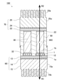
- FIG. 7 is a cross-sectional view schematically showing the power module 100 according to the embodiment of the present invention.
- FIG. 8 is an enlarged view showing a cross-sectional structure of a region of the power module 100 in which the power semiconductor chip 1 is provided.
- the description may be made assuming that the positional relationship (upper and lower relationship, etc.) of each component of the power module 100 is the relationship shown in each figure. However, the positional relationship in this description is irrelevant to the positional relationship when the power module 100 is used or manufactured.
- the power module 100 is provided on one surface side (lower surface 1a side in the drawing) of the power semiconductor chip 1, a lead frame 6 that supports and fixes the power semiconductor chip 1 and electrically connects to an external wiring, and the power semiconductor chip 1.
- the sealing material layer 50 is provided in the space between the first heat dissipation structure 60 and the second heat dissipation structure 70.
- the power module 100 includes a power semiconductor chip 1, a first bonding layer 12 connecting the lead frame 6 and the first heat radiating structure 60, and a second bonding layer 22 connecting the spacer 30 and the second heat radiating structure 70. It has a third bonding layer 32 that connects the power semiconductor chip 1 and the spacer 30.
- a specific description will be given.
- the power semiconductor chip 1 is, for example, an insulated gate bipolar transistor (IGBT), a diode, or the like.
- An electrode pattern (not shown) is formed on the upper surface of the power semiconductor chip 1, and a conductive pattern (not shown) is formed on the lower surface 1a of the power semiconductor chip 1.
- the lower surface 1a of the power semiconductor chip 1 is bonded to the first heat dissipation structure 60 via the first bonding layer 12, which is a bonding layer.
- the electrode pattern on the upper surface 1b of the power semiconductor chip 1 is electrically connected to the lead frame 6.
- the lead frame 6 supports and fixes the power semiconductor chip 1 and is electrically connected to external wiring, and is a component made by pressing or etching a thin plate of a metal material such as copper or iron. Is.
- the first heat dissipation structure 60 includes a first Cu circuit 13 (also referred to as a “first metal circuit board”), a first heat dissipation sheet 14, and a first heat sink 15 (“first”) from the power semiconductor chip 1 side. It also has a heat dissipation member).
- the first Cu circuit 13 is a metal circuit board made of a conductive metal material.
- a power semiconductor chip 1 is provided in a circuit pattern formed on one surface (upper surface in the drawing) of the first Cu circuit 13 via the first junction layer 12.
- the first Cu circuit 13 is a circuit board in which thick copper (rolled copper) is patterned.
- thick copper rolled copper
- the resistance value of the first Cu circuit 13 becomes relatively small.
- At least a part of the first Cu circuit 13 may be covered with a solder resist layer.
- the first Cu circuit 13 processes, for example, a metal layer (thick copper or the like) laminated on the upper surface of the base portion 15a of the first heat sink 15 (Cu base plate) via the first heat dissipation sheet 14 into a predetermined pattern by cutting and etching. It is formed by the above-mentioned, or is attached to the first Cu circuit 13 by the first heat dissipation sheet 14 in a state of being processed into a predetermined pattern in advance.
- the lower limit of the thickness of the first Cu circuit 13 is, for example, 0.3 mm or more. If it is more than such a value, heat generation of the first Cu circuit 13 can be suppressed even in an application requiring a high current.
- the upper limit of the thickness of the first Cu circuit 13 is, for example, 5.0 mm or less, preferably 4.0 mm or less, and more preferably 3.0 mm or less. If it is less than such a numerical value, the circuit workability can be improved, and the thickness of the product as a whole can be reduced.
- the first heat dissipation sheet 14 is arranged between the first Cu circuit 13 and the first heat sink 15 (Cu base plate).
- the heat of the power semiconductor chip 1 is received by the first Cu circuit 13, and further transferred to the first heat sink 15 (Cu base plate) which is a heat radiating means via the first heat radiating sheet 14.
- heat generated from the power semiconductor chip 1 which is a heating element can be effectively dissipated to the outside of the power module 100 while maintaining the insulating property of the power module 100. Therefore, it is possible to improve the insulation reliability of the semiconductor device.
- the planar shape of the first heat dissipation sheet 14 is not particularly limited, and can be appropriately selected according to the shape of the first Cu circuit 13 and the first heat sink 15, but can be, for example, a rectangle.
- the film thickness of the first heat radiating sheet 14 is, for example, 50 ⁇ m or more and 250 ⁇ m or less. As a result, the heat of the first Cu circuit 13 can be more effectively transferred to the first heat sink 15 while improving the mechanical strength and heat resistance. Further, the balance between heat dissipation and insulation of the first heat dissipation sheet 14 is excellent.
- the thermal conductivity of the first heat radiating sheet 14 is not particularly limited, but preferably 10 W / mK (175 ° C.) or higher, more preferably 15 W / mK (175 ° C.) or higher.
- the first heat radiating sheet 14 is, for example, a resin sheet, and is formed by using a resin composition for a sheet.
- the sheet resin composition described in the first embodiment can be used as the sheet resin composition, and the description thereof will be omitted below.
- the first heat sink 15 is a kind of heat dissipation member also called a Cu base plate, and has a copper plate-shaped base portion 15a and a plurality of fin portions 15B integrally extending from the lower surface of the base portion 15a.
- an aluminum base plate may be adopted in addition to the Cu base plate.
- it is not limited to a general heat dissipation member, but may be a part of other configurations (for example, a housing). You may. Even in that case, the first heat dissipation sheet 14 can be used.
- the first bonding layer 12 is a bonding layer obtained by sintering a sintered paste containing metal particles.
- a sintered paste containing metal particles any one of an Ag sintering paste containing silver particles, an AL sintering paste containing aluminum particles, and a Cu sintering paste containing copper particles can be used.
- a sintering paste as described above is provided between the power semiconductor chip 1 and the first Cu circuit 13 and laminated, and the power semiconductor chip 1 and the first Cu circuit 13 are bonded by the first bonding layer 12 by a sintering step. ..
- the first Cu circuit 13 and the lead frame 6 are joined by the first joining layer 12.
- a syntaring network metal bonding bus
- the first Cu circuit 13 and the lead frame 6 may be surface-treated by plating with a metal contained in the sintering paste.
- the surface of the first Cu circuit 13 or the lead frame 6 may be subjected to Ag plating.
- the second heat dissipation structure 70 includes a second Cu circuit 23 (also referred to as a “second metal circuit board”), a second heat dissipation sheet 24, and a second from the power semiconductor chip 1 side (that is, the spacer 30 side). It has a heat sink 25 (also referred to as a "second heat dissipation member").
- the second Cu circuit 23 is a metal circuit board made of a conductive metal material.
- the circuit pattern formed on one surface (lower surface in the drawing) of the second Cu circuit 23 is bonded to the spacer 30 via the second bonding layer 22. Further, in the region where the spacer 30 is not provided, the spacer 30 is joined to the encapsulant layer 50.
- the second Cu circuit 23 may be a circuit board in which thick copper (rolled copper) is patterned, or may be configured in which thick copper is used as it is without patterning.
- thick copper rolled copper
- the resistance value of the second Cu circuit 23 becomes relatively small.
- At least a part of the second Cu circuit 23 may be covered with a solder resist layer.
- the second Cu circuit 23 processes, for example, a metal layer (thick copper or the like) laminated on the lower surface of the base portion 25a of the second heat sink 25 (Cu base plate) via the second heat dissipation sheet 24 into a predetermined pattern by cutting and etching.
- the second Cu circuit 23 is attached to the second Cu circuit 23 by the second heat radiating sheet 24 in a state of being formed by the above or processed in advance into a predetermined pattern.
- the lower limit of the thickness of the second Cu circuit 23 is, for example, 0.3 mm or more. If it is more than such a value, heat generation of the second Cu circuit 23 can be suppressed even in an application requiring a high current.
- the upper limit of the thickness of the second Cu circuit 23 is, for example, 5.0 mm or less, preferably 4.0 mm or less, and more preferably 3.0 mm or less. If it is less than such a numerical value, the circuit workability can be improved, and the thickness of the product as a whole can be reduced.
- the second heat dissipation sheet 24 is arranged between the second Cu circuit 23 and the second heat sink 25 (Cu base plate).
- the heat of the power semiconductor chip 1 is received by the second Cu circuit 23 via the spacer 30, and further transferred to the second heat sink 25 which is a heat radiating means via the second heat radiating sheet 24.
- heat generated from the power semiconductor chip 1 which is a heating element can be effectively dissipated to the outside of the power module 100 while maintaining the insulating property of the power module 100. Therefore, it is possible to improve the insulation reliability of the semiconductor device.
- the shape and physical properties of the second heat radiating sheet 24 are the same as those of the first heat radiating sheet 14 described above. That is, the planar shape of the second heat radiating sheet 24 is not particularly limited and can be appropriately selected according to the shape of the second Cu circuit 23 or the second heat sink 25, but can be, for example, a rectangle.
- the film thickness of the second heat radiating sheet 24 is, for example, 50 ⁇ m or more and 250 ⁇ m or less. As a result, the heat of the second Cu circuit 23 can be more effectively transferred to the second heat sink 25 while improving the mechanical strength and heat resistance. Further, the balance between heat dissipation and insulation of the second heat dissipation sheet 24 is excellent.
- the thermal conductivity of the second heat radiating sheet 24 is not particularly limited, but preferably 10 W / mK (175 ° C.) or higher, more preferably 15 W / mK (175 ° C.) or higher.
- the material of the second heat radiating sheet 24 the material described in the material of the first heat radiating sheet 14 can be used.
- the materials and film thicknesses of the first heat radiating sheet 14 and the second heat radiating sheet 24 may be exactly the same, or may be different within the above range.
- the second heat sink 25 is a kind of heat dissipation member also called a Cu base plate, and has a copper plate-shaped base 25a and a plurality of fin portions 25b extending integrally from the upper surface of the base 25a.
- the second heat sink 25 for example, an aluminum base plate may be adopted in addition to the Cu base plate.
- it has a function of acquiring heat generated by the power semiconductor chip 1 via the spacer 30 and the second Cu circuit 23 and releasing it to others, it is not limited to a general heat dissipation member, but a part of other configurations (for example, a housing). And so on. Even in that case, the second heat dissipation sheet 24 can be used.
- the second bonding layer 22 is a bonding layer obtained by sintering a sintered paste containing metal particles, similarly to the first bonding layer 12.
- a sintered paste containing metal particles similarly to the first bonding layer 12.
- the sintering paste any one of an Ag sintering paste containing silver particles, an AL sintering paste containing aluminum particles, and a Cu sintering paste containing copper particles can be used.
- a sintering paste as described above is provided between the spacer 30 and the second Cu circuit 23 and laminated, and the spacer 30 and the second Cu circuit 23 are bonded by the second bonding layer 22 by a sintering step.
- the spacer 30 adjusts the distance between the power semiconductor chip 1 and the second heat dissipation structure 70 arranged on the upper side of the power semiconductor chip 1 to a predetermined length.
- the spacer 30 is made of metal, for example, and specifically, copper (including a copper alloy), aluminum (including an aluminum alloy), and the like.
- the upper side of the spacer 30 is bonded to the second Cu circuit 23 of the second heat dissipation structure 70 via the second bonding layer 22. Further, the lower side of the spacer 30 is bonded to the power semiconductor chip 1 via the third bonding layer 32 described later.
- the spacer 30 can adjust the heat dissipation characteristics of the power semiconductor chip 1 in the upper direction. Further, when forming the encapsulant layer 50 for encapsulating the power semiconductor chip 1, the lead frame 6, and the like, the flow of the encapsulant can be appropriately adjusted.
- the third bonding layer 32 is a bonding layer obtained by sintering a sintered paste containing metal particles, similarly to the first bonding layer 12 and the second bonding layer 22.
- a sintered paste containing metal particles similarly to the first bonding layer 12 and the second bonding layer 22.
- the sintering paste any one of an Ag sintering paste containing silver particles, an AL sintering paste containing aluminum particles, and a Cu sintering paste containing copper particles can be used.
- a sintering paste as described above is provided between the spacer 30 and the power semiconductor chip 1 and laminated, and the spacer 30 and the power semiconductor chip 1 are bonded by a third bonding layer 32 by a sintering step.
- the sealing material layer 50 is, for example, a mold resin, and the components between the first heat radiating structure 60 and the second heat radiating structure 70, such as the power semiconductor chip 1 and the spacer 30, are integrally sealed inside. ing.
- a silicone gel or the like may be used in addition to the mold resin.
- the first heat sink 15 covers and seals the power semiconductor chip 1 so as to cover a part or all of the side surface of the base portion 15a of the first heat sink 15 in the thickness direction.
- the configuration in which all the side surfaces of the base portion 15a of the first heat sink 15 are covered with the sealing material layer 50 is illustrated.
- the thermal resistance in the laminated structure of the power module 100 will be described.
- the ratio R1 / R2 to the thermal resistance R2 is 0.7 or more and 1.3 or less, preferably 0.8 or more and 1.2 or less, and more preferably 0.9 or more and 1.1 or less.
- the first thermal resistance R1 and the second thermal resistance R2 are 0.05 K / W or more and 0.5 K / W or less, preferably 0.06 K / W or more and 0.45 K / W or less, and more preferably 0. It is 0.7 K / W or more and 0.40 K / W or less.
- the first thermal resistance R1 is the thermal resistance R11 of the lower half in the thickness direction of the spacer 30, the thermal resistance R12 of the third junction layer 32, the thermal resistance R13 of the power semiconductor chip 1, and the first junction layer 12. It is the total (R11 + R12 + R13 + R14 + R15) of the thermal resistance R14 and the thermal resistance R15 of the first heat dissipation structure 60.
- the thermal resistance R15 of the first heat dissipation structure 60 is the total (R16 + R17 + R18) of the thermal resistance R16 of the first Cu circuit 13, the thermal resistance R17 of the first heat dissipation sheet 14, and the thermal resistance R18 of the first heat sink 15.
- the second thermal resistance R2 is the total (R21 + R22 + R23) of the thermal resistance R21 of the upper half in the thickness direction of the spacer 30, the thermal resistance R22 of the second bonding layer 22, and the thermal resistance R23 of the second heat dissipation structure 70.
- the thermal resistance R23 of the second heat dissipation structure 70 is the total (R24 + R25 + R26) of the thermal resistance R24 of the second Cu circuit 23, the thermal resistance R25 of the second heat dissipation sheet 24, and the thermal resistance R26 of the second heat sink 25.
- the power module 100 of this embodiment is Power semiconductor chip 1 and The first heat dissipation structure 60 provided on one surface side (the side of the lower surface 1a in the figure) of the power semiconductor chip 1 and The second heat dissipation structure 70 provided on the other surface side (the side of the upper surface 1b in the figure) of the power semiconductor chip 1 and A first bonding layer 12 for bonding the power semiconductor chip 1 and the first heat dissipation structure 60 with a sintering paste, and A spacer 30 provided between the power semiconductor chip 1 and the second heat dissipation structure 70, A second bonding layer 22 for bonding the second heat dissipation structure 70 and the spacer 30 with a sintering paste, and A third bonding layer 32 for bonding the power semiconductor chip 1 and the spacer 30 with a sintering paste, and In the region between the first heat radiating structure 60 and the second heat radiating structure 70, the region
- the heat dissipation performance of the power module 100 can be improved.
- the power semiconductor chip 1 is bonded to the first bonding layer 12 and the spacer 30, and the spacer 30 is bonded to the second heat dissipation structure 70 (that is, the second Cu circuit 23).
- the first to third bonding layers 12, 22, and 32 using the above were used. Since the sintering layer (sintering paste) has a high thermal conductivity, the heat generated by the power semiconductor chip 1 can be effectively released to the outside.
- the spacer 30 between the upper surface 1b of the power semiconductor chip 1 and the second heat dissipation structure 70 it is possible to adjust the heat dissipation characteristics in the upper direction of the power semiconductor chip 1. Further, when forming the encapsulant layer 50 for encapsulating the power semiconductor chip 1, the lead frame 6, and the like, the flow of the encapsulant can be appropriately adjusted. Further, by using the sealing material layer 50 as a mold resin, it becomes easier to cope with the miniaturization and the thinning of the power module having the power semiconductor chip 1.
- the first heat dissipation structure 60 is A first metal circuit board (first Cu circuit 13) to be joined to one surface of the first joining layer 12 and the like.
- a first heat dissipation sheet 14 provided on the other surface of the first metal circuit board (first Cu circuit 13) and provided for joining the first heat sink 15.
- the heat generated by the power semiconductor chip 1 can be effectively released to the outside (particularly from the lower side in the drawing).
- the maximum temperature of the power semiconductor chip 1 can be lowered, and the electrical characteristics can be improved.
- the thermal stress in continuous use is reduced, and the reliability of the joint portion such as the first joint layer 12 and the first heat dissipation sheet 14 is improved.
- the first heat dissipation structure 60 has the first heat sink 15.
- the second heat dissipation structure 70 is A second metal circuit board (second Cu circuit 23) bonded to one surface of the second bonding layer 22 and the like.
- a second heat radiating sheet 24 provided on the other surface of the second metal circuit board (second Cu circuit 23) for joining the second heat sink 25.
- the second heat dissipation structure 70 has the second heat sink 25.
- the ratio R1 / R2 to the second thermal resistance R2 in the stacking direction is 0.7 or more and 1.3 or less.
- the first thermal resistance R1 and the second thermal resistance R2 are 0.05 (K / W) or more and 0.5 (K / W) or less.
- the power module of the present invention is Power semiconductor devices and A first heat dissipation structure in which the power semiconductor element is provided on one side, Have,
- the first heat dissipation structure is The first metal circuit board and A first bonding layer provided for bonding the power semiconductor element to one surface of the first metal circuit board with a sintering paste,
- a first heat dissipation sheet provided for joining the first heat dissipation member to the other surface of the first metal circuit board, and Have
- the total thermal resistance in the lamination direction is 0.30 (K /).
- the first heat dissipation structure is Further, a first heat radiating member joined by the first heat radiating sheet is provided on the other surface of the first metal circuit board.
- the stacking direction high.
- the total thermal resistance in the vertical direction is 0.45 (K / W) or less.
- the ratio XA / tA is 0.25. (W / (K ⁇ mm)) or less.
- a second heat dissipation structure provided on the other surface side of the power semiconductor element, and a spacer provided between the power semiconductor element and the second heat dissipation structure. Further have The second heat dissipation structure includes a second metal circuit board and a second bonding layer provided for bonding the spacer to one surface of the second metal circuit board with a sintering paste.
- a third bonding layer for bonding the power semiconductor element and the spacer with a sintering paste In the region between the first heat dissipation structure and the second heat dissipation structure, the region where the power semiconductor element, the spacer, and the first to third bonding layers are not provided is sealed with a mold encapsulant.
- the second heat dissipation structure is Further having a second heat radiating sheet provided for joining the second heat radiating member to the other surface of the second metal circuit board.
- the second heat dissipation structure is Further, a second heat radiating member joined by the second heat radiating sheet is provided on the other surface of the second metal circuit board.
- the ratio R1 / R2 to the thermal resistance R2 is 0.7 or more and 1.3 or less.
- the first thermal resistance R1 and the second thermal resistance R2 are 0.05 (K / W) or more and 0.5 (K / W) or less.
- the metal particles contained in the sintering paste are either silver particles, aluminum particles or copper particles.
- a sealing material for covering the power semiconductor element is provided.
- the sealing material is made of a mold resin.
- the sealing material covers and seals the power semiconductor element so as to cover a part or all of the side surface in the thickness direction of the first heat radiating member and / or the second heat radiating member.
- the first metal circuit board and / or the second metal circuit board is a circuit board in which thick copper (rolled copper) is patterned, and the thickness is 0.3 mm or more and 5 mm or less.
- first and second embodiments correspond to the first embodiment
- third embodiment corresponds to the second embodiment.
- Table 1 illustrates the thermal conductivity of the above-mentioned first and second laminated structure examples (Examples 1 and 2) together with the thermal conductivity of the comparative example.
- the thickness t of the configuration corresponding to the Cu circuit 3 is different between the first embodiment and the second embodiment, and the other conditions are the same.
- the element corresponding to the first laminated structure is a laminated structure by "chip, sintering, circuit, heat dissipation sheet”.
- the element corresponding to the second laminated structure is a laminated structure consisting of "chips, sinterings, circuits, heat dissipation sheets, and base substrates".
- the heat radiating sheet the resin sheet of the heat radiating sheet 14 described in the above-described embodiment having a thermal conductivity of 18 W was applied.
- the total Rth_sum (corresponding to XA (W / K) of the embodiment) of the thermal resistance in the stacking direction of the first laminated structure in Examples 1 and 2 is 0.119 (W / K) and 0.168 (W, respectively). / K), that is, 0.30 (W / K) or less.
- the configuration excluding the base substrate (corresponding to the first laminated structure) is 0.353 (W / K), that is, exceeds 0.30 (W / K).
- the total Rth_sum (corresponding to XB (W / K) of the embodiment) of the thermal resistance in the stacking direction of the second laminated structure in Examples 1 and 2 is 0.184 (W / K) and 0.233 (W), respectively. / K), that is, 0.25 (W / K) or less. On the other hand, in the configuration including the base substrate of the comparative example, it is 0.473 (W / K), that is, it exceeds 0.45 (W / K).
- XA / t is 0.156 (W / (K ⁇ mm)) and 0.074 (W / (K ⁇ mm)), respectively, that is, 0.25 (W / K) or less.
- the configuration excluding the base substrate (corresponding to the first laminated structure) is 0.257 (W / (K ⁇ mm)), that is, 0.25 (W / (K ⁇ mm)).
- XB / tB) is 0.067 (W / (K ⁇ mm)) and 0.055 (W / (K ⁇ mm)), respectively, that is, 0.08 (W / K) or less.
- it is 0.083 (W / (K ⁇ mm)), that is, it exceeds 0.08 (W / (K ⁇ mm)).
- FIG. 2 shows a structural example of the power modules of the examples and the comparative examples in a cross-sectional view.
- FIGS. 3 to 5 and Table 2 show the physical property values and dimensions (thickness) of each component of the simulation example and the comparative example.
- FIG. 3A is a perspective view of the power module as viewed from above, and FIG. 3B is a plan view.
- FIG. 4A is a perspective view seen from the lower side of the power module, and FIG. 4B is a bottom view.
- FIG. 5 is a diagram showing thermal conditions in a simulation (heat transfer analysis).
- Simulation software ANSYS Mechanical 2019R3 Power semiconductor chip: Base substrate equipped with IGBT and FWD (Free Wheeling Diode): A convex pole is provided on the Cu base plate, and the back of the Cu base plate and the surface of the convex pole are cooled with cooling water (65 ° C).
- FIG. 6 shows the heat distribution on the model of the power module as a simulation result.
- the maximum temperature of the surface of the power semiconductor chip here, the IGBT
- the maximum temperature of the surface of the power semiconductor chip here, the IGBT
- the configuration of the embodiment corresponding to the first thermal resistance R1 includes a spacer 30 (lower half), a power semiconductor chip 1 (Si-IGBT), a first bonding layer 12 (sintering paste layer), a first Cu circuit 13, and the like.
- the first heat dissipation sheet 14 and the first heat sink 15 (Cu) are laminated.
- the simulation is performed with a configuration in which the third bonding layer 32 is omitted.
- the configuration of the embodiment corresponding to the second thermal resistance R2 includes a spacer 30 (upper half), a second bonding layer 22 (sintering paste layer), a second Cu circuit 23, a second heat dissipation sheet 24, and a second heat sink 25 (the second heat sink 25 (upper half). It is a structure in which Cu) is laminated.
- the first thermal resistance R1 and the second thermal resistance R2 were in the range of 0.05 (K / W) or more and 0.5 (K / W) or less.
- the ratio R1 / R2 was 0.7 or more and 1.3 or less.
Abstract
A power module (10) has a power conductor chip (1) and a Cu circuit (3) in which the power conductor chip (1) is provided on one surface. The power module (10) has: a sintering layer (2) in which the power conductor chip (1) and the Cu circuit (3) are joined with sintering paste; and a heat radiation sheet (4) provided to join a Cu base plate (5) to the other surface of the Cu circuit (3), and in a first layered structure in which the power semiconductor chip (1), the sintering layer (2), the Cu circuit (3), and the heat radiation sheet (4) are layered, the total XA of the heat resistance in the layering direction is 0.30 (K/W) or less.
Description
本発明は、パワーモジュールに係り、例えばパワー半導体素子と、パワー半導体素子を一方の面に設けた金属回路基板(伝熱金属層)と、を有すパワーモジュールに関する。
The present invention relates to a power module, and relates to a power module having, for example, a power semiconductor element and a metal circuit board (heat transfer metal layer) having the power semiconductor element provided on one surface.
パワー半導体素子を伝熱用の金属回路基板を設けたパワーモジュールの市場が拡大している。そのようなパワーモジュールでは、高い放熱性を実現するために各種の技術が提案されている。例えば、高熱伝導性のフィラーと結晶性ポリマーとを含み、一体成形されたフィン付きヒートシンクおよび基材と、前記基材上に形成され、絶縁性の熱伝導性フィラーと結晶性ポリマーとを含む絶縁層と、前記絶縁層上に形成された金属層とを有し、前記フィン付きヒートシンクおよび基材中の高熱伝導性フィラーの含有率が15~65vol%であり、前記絶縁層中の熱伝導性フィラーの含有率が15~65vol%であるフィン付きヒートシンク一体回路基板用積層板が知られている(例えば、特許文献1参照)。
The market for power modules equipped with metal circuit boards for heat transfer of power semiconductor elements is expanding. In such a power module, various techniques have been proposed in order to realize high heat dissipation. For example, an insulation comprising a highly thermally conductive filler and a crystalline polymer, integrally molded with a finned heat sink and a substrate, and an insulating thermally conductive filler and a crystalline polymer formed on the substrate. It has a layer and a metal layer formed on the insulating layer, and the content of the high thermal conductive filler in the finned heat sink and the base material is 15 to 65 vol%, and the thermal conductivity in the insulating layer is 15 to 65 vol%. A laminated plate for a heat sink integrated circuit board with fins having a filler content of 15 to 65 vol% is known (see, for example, Patent Document 1).
しかしながら、従来のパワーモジュール構造では、「チップ(パワー半導体素子)/はんだ/DBC(Direct Bonded Copper)基板/はんだ/放熱フィン」といった積層構造となっていた。チップ(パワー半導体素子)とDBC基板の接合および、DBC基板と放熱フィンの接合には、はんだを使用していた。パワーモジュールが動作した際に、チップ(パワー半導体素子)が発熱するが、上述の構造ではその放熱が十分ではなく、対策の技術が求められていた。
However, the conventional power module structure has a laminated structure such as "chip (power semiconductor element) / solder / DBC (Direct Bonded Copper) substrate / solder / heat dissipation fin". Solder was used for joining the chip (power semiconductor element) and the DBC board and joining the DBC board and the heat radiation fins. When the power module operates, the chip (power semiconductor element) generates heat, but the above-mentioned structure does not sufficiently dissipate heat, and a countermeasure technique has been required.
本発明はこの様な状況に鑑みなされたものであって、パワー半導体素子を備えるパワーモジュールにおいて、放熱性能を向上させることを目的とする。
The present invention has been made in view of such a situation, and an object of the present invention is to improve heat dissipation performance in a power module including a power semiconductor element.
本発明によれば、パワー半導体素子と、
前記パワー半導体素子を一方の面側に設けた第1放熱構造と、
を有し、
前記第1放熱構造は、
第1金属回路基板と、
前記パワー半導体素子を前記第1金属回路基板の一方の面にシンタリングペーストにより接合するために設けた第1接合層と、
前記第1金属回路基板の他方の面に第1放熱部材を接合するために設けた第1放熱シートと、
を有し、
前記パワー半導体素子と、前記第1接合層と、前記第1金属回路基板と、前記第1放熱シートとが積層された積層構造Aにおいて、積層方向の熱抵抗の合計が0.30(K/W)以下である、
パワーモジュールが提供される。 According to the present invention, a power semiconductor device and
A first heat dissipation structure in which the power semiconductor element is provided on one side,
Have,
The first heat dissipation structure is
The first metal circuit board and
A first bonding layer provided for bonding the power semiconductor element to one surface of the first metal circuit board with a sintering paste,
A first heat dissipation sheet provided for joining the first heat dissipation member to the other surface of the first metal circuit board, and
Have,
In the laminated structure A in which the power semiconductor element, the first junction layer, the first metal circuit board, and the first heat dissipation sheet are laminated, the total thermal resistance in the lamination direction is 0.30 (K /). W) Below,
A power module is provided.
本発明によれば、パワー半導体素子を備えるパワーモジュールにおいて、放熱性能を向上させる技術を提供できる。
According to the present invention, it is possible to provide a technique for improving heat dissipation performance in a power module including a power semiconductor element.
以下、本発明の実施形態について、図面を参照しつつ、詳細に説明する。図面はあくまで説明用のものである。図面中の各部材の形状や寸法比などは、必ずしも現実の物品と対応するものではない。
Hereinafter, embodiments of the present invention will be described in detail with reference to the drawings. The drawings are for illustration purposes only. The shape and dimensional ratio of each member in the drawing do not necessarily correspond to the actual article.
<<第1の実施形態>>
<発明の概要>
<パワーモジュール10>
本実施形態に係るパワーモジュール10について説明する。図1は、本発明の実施形態に係るパワーモジュール10を模式的に示した断面図である。以下では、説明を簡単にするため、パワーモジュール10の各構成要素の位置関係(上下関係等)が各図に示す関係であるものとして説明を行う場合がある。ただし、この説明における位置関係は、パワーモジュール10の使用時や製造時の位置関係とは無関係である。 << First Embodiment >>
<Outline of the invention>
<Power module 10>
The power module 10 according to this embodiment will be described. FIG. 1 is a cross-sectional view schematically showing a power module 10 according to an embodiment of the present invention. In the following, for the sake of simplicity, the description may be made assuming that the positional relationship (upper and lower relationship, etc.) of each component of the power module 10 is the relationship shown in each figure. However, the positional relationship in this description is irrelevant to the positional relationship when the power module 10 is used or manufactured.
パワーモジュール10は、パワー半導体チップ(パワー半導体素子ともいう)1と、シンタリング層2(「第1接合層」ともいう)と、Cu回路3(「第1金属回路基板」ともいう)と、放熱シート4と、Cuベースプレート5(「第1放熱部材」ともいう)と、リードフレーム6と、封止材7とを有する。
The power module 10 includes a power semiconductor chip (also referred to as a power semiconductor element) 1, a sintering layer 2 (also referred to as a “first junction layer”), and a Cu circuit 3 (also referred to as a “first metal circuit board”). It has a heat radiating sheet 4, a Cu base plate 5 (also referred to as a "first heat radiating member"), a lead frame 6, and a sealing material 7.
<パワー半導体チップ1>
パワー半導体チップ1は、例えば、絶縁ゲートバイポーラトランジスタ(IGBT;Insulated Gate Bipolar Transistor)およびダイオード等である。パワー半導体チップ1の上面には図示しない電極パターンが形成され、パワー半導体チップ1の下面には図示しない導電パターンが形成されている。
パワー半導体チップ1の下面は、接合層であるシンタリング層2を介してCu回路3の一方の面に接合されている。パワー半導体チップ1の上面の電極パターンは、リードフレーム6に対して電気的に接続されている。 <Power semiconductor chip 1>
Thepower semiconductor chip 1 is, for example, an insulated gate bipolar transistor (IGBT), a diode, or the like. An electrode pattern (not shown) is formed on the upper surface of the power semiconductor chip 1, and a conductive pattern (not shown) is formed on the lower surface of the power semiconductor chip 1.
The lower surface of thepower semiconductor chip 1 is bonded to one surface of the Cu circuit 3 via the sintering layer 2, which is a bonding layer. The electrode pattern on the upper surface of the power semiconductor chip 1 is electrically connected to the lead frame 6.
パワー半導体チップ1は、例えば、絶縁ゲートバイポーラトランジスタ(IGBT;Insulated Gate Bipolar Transistor)およびダイオード等である。パワー半導体チップ1の上面には図示しない電極パターンが形成され、パワー半導体チップ1の下面には図示しない導電パターンが形成されている。
パワー半導体チップ1の下面は、接合層であるシンタリング層2を介してCu回路3の一方の面に接合されている。パワー半導体チップ1の上面の電極パターンは、リードフレーム6に対して電気的に接続されている。 <
The
The lower surface of the
<シンタリング層2>
シンタリング層2は、金属粒子が含有されたシンタリングペーストを焼結させ接合層である。シンタリングペーストとしては、銀粒子を含有するAgシンタリングペースト、アルミニウム粒子を含有するALシンタリングペースト、銅粒子を含有するCuシンタリングペーストのいずれかを用いることができる。 <Sintering layer 2>
Thesintering layer 2 is a bonding layer obtained by sintering a sintering paste containing metal particles. As the sintering paste, any one of an Ag sintering paste containing silver particles, an AL sintering paste containing aluminum particles, and a Cu sintering paste containing copper particles can be used.
シンタリング層2は、金属粒子が含有されたシンタリングペーストを焼結させ接合層である。シンタリングペーストとしては、銀粒子を含有するAgシンタリングペースト、アルミニウム粒子を含有するALシンタリングペースト、銅粒子を含有するCuシンタリングペーストのいずれかを用いることができる。 <
The
パワー半導体チップ1とCu回路3との間に上記のようなシンタリングペーストを設けて積層し、焼結工程により、パワー半導体チップ1とCu回路3がシンタリング層2により接合される。Cu回路3とリードフレーム6とがシンタリング層2により接合されている。
シンタリング層2では、金属粒子によるシンタリングネットワーク(金属結合バス)が形成されており、高熱伝導性や低い電気抵抗が実現される。なお、シンタリング層2による接合性の向上の観点から、Cu回路3やリードフレーム6に、シンタリングペーストに含有される金属によるメッキの表面処理が施されてもよい。具体的には、本実施形態では、Cu回路3やリードフレーム6の表面にAgメッキが施されてもよい。 A sintering paste as described above is provided between thepower semiconductor chip 1 and the Cu circuit 3 and laminated, and the power semiconductor chip 1 and the Cu circuit 3 are bonded by the sintering layer 2 by a sintering step. The Cu circuit 3 and the lead frame 6 are joined by a sintering layer 2.
In thesintering layer 2, a sintering network (metal bonding bus) made of metal particles is formed, and high thermal conductivity and low electrical resistance are realized. From the viewpoint of improving the bondability by the sintering layer 2, the Cu circuit 3 and the lead frame 6 may be surface-treated by plating with a metal contained in the sintering paste. Specifically, in the present embodiment, the surface of the Cu circuit 3 or the lead frame 6 may be subjected to Ag plating.
シンタリング層2では、金属粒子によるシンタリングネットワーク(金属結合バス)が形成されており、高熱伝導性や低い電気抵抗が実現される。なお、シンタリング層2による接合性の向上の観点から、Cu回路3やリードフレーム6に、シンタリングペーストに含有される金属によるメッキの表面処理が施されてもよい。具体的には、本実施形態では、Cu回路3やリードフレーム6の表面にAgメッキが施されてもよい。 A sintering paste as described above is provided between the
In the
<Cu回路3>
Cu回路3は、導電性を有する金属材料で構成された金属回路基板である。Cu回路3の一方の面(図示で上側の面)に形成された回路パターンに、接合層であるシンタリング層2を介して、パワー半導体チップ1が設けられている。 <Cu circuit 3>
TheCu circuit 3 is a metal circuit board made of a conductive metal material. A power semiconductor chip 1 is provided on a circuit pattern formed on one surface (upper surface in the drawing) of the Cu circuit 3 via a sintering layer 2 which is a bonding layer.
Cu回路3は、導電性を有する金属材料で構成された金属回路基板である。Cu回路3の一方の面(図示で上側の面)に形成された回路パターンに、接合層であるシンタリング層2を介して、パワー半導体チップ1が設けられている。 <
The
Cu回路3は、厚銅(圧延銅)をパターンニングした回路基板であって、例えば厚みが0.3mm以上5mm以下である。Cu回路3を構成する金属材料には、例えば、厚銅(圧延銅)を好適に用いることができる。これにより、Cu回路3は、比較的抵抗値が小さくなる。なお、Cu回路3は、その少なくとも一部がソルダーレジスト層で覆われていてもよい。
The Cu circuit 3 is a circuit board in which thick copper (rolled copper) is patterned, and has a thickness of, for example, 0.3 mm or more and 5 mm or less. For example, thick copper (rolled copper) can be preferably used as the metal material constituting the Cu circuit 3. As a result, the resistance value of the Cu circuit 3 becomes relatively small. At least a part of the Cu circuit 3 may be covered with a solder resist layer.
Cu回路3は、例えば、Cuベースプレート5の基部5Aの上面に放熱シート4を介して積層された金属層(厚銅など)を切削及びエッチングにより所定のパターンに加工することにより形成されたり、または予め所定のパターンに加工された状態で放熱シート4によりCu回路3に貼りつけられる。
The Cu circuit 3 is formed, for example, by processing a metal layer (thick copper or the like) laminated on the upper surface of the base 5A of the Cu base plate 5 via a heat dissipation sheet 4 into a predetermined pattern by cutting and etching. It is attached to the Cu circuit 3 by the heat radiating sheet 4 in a state of being processed into a predetermined pattern in advance.
Cu回路3の厚さの下限値は、例えば、0.3mm以上である。このような数値以上であれば、高電流を要する用途であっても、回路パターンの発熱を抑えることができる。また、回路パターン20の厚さの上限値は、例えば、5.0mm以下であり、好ましくは4.0mm以下であり、さらに好ましくは3.0mm以下である。このような数値以下であれば、回路加工性を向上させることができ、また、基板全体としての薄型化を図ることができる。
The lower limit of the thickness of the Cu circuit 3 is, for example, 0.3 mm or more. If it is more than such a value, it is possible to suppress heat generation of the circuit pattern even in an application requiring a high current. The upper limit of the thickness of the circuit pattern 20 is, for example, 5.0 mm or less, preferably 4.0 mm or less, and more preferably 3.0 mm or less. If it is less than such a numerical value, the circuit workability can be improved, and the thickness of the entire substrate can be reduced.
<放熱シート4>
放熱シート4は、Cu回路3とCuベースプレート5の間に配置される。パワー半導体チップ1の熱をCu回路3で受け、さらに、放熱シート4を介して放熱手段であるCuベースプレート5に伝熱される。これにより、パワーモジュール10の絶縁性を保ちつつ、発熱体であるパワー半導体チップ1から生じる熱を、パワーモジュール10の外部へ効果的に放散させることができる。このため、半導体装置の絶縁信頼性を向上させることが可能となる。 <Heat dissipation sheet 4>
The heat dissipation sheet 4 is arranged between theCu circuit 3 and the Cu base plate 5. The heat of the power semiconductor chip 1 is received by the Cu circuit 3, and further, the heat is transferred to the Cu base plate 5 which is a heat radiating means via the heat radiating sheet 4. As a result, the heat generated from the power semiconductor chip 1 which is a heating element can be effectively dissipated to the outside of the power module 10 while maintaining the insulating property of the power module 10. Therefore, it is possible to improve the insulation reliability of the semiconductor device.
放熱シート4は、Cu回路3とCuベースプレート5の間に配置される。パワー半導体チップ1の熱をCu回路3で受け、さらに、放熱シート4を介して放熱手段であるCuベースプレート5に伝熱される。これにより、パワーモジュール10の絶縁性を保ちつつ、発熱体であるパワー半導体チップ1から生じる熱を、パワーモジュール10の外部へ効果的に放散させることができる。このため、半導体装置の絶縁信頼性を向上させることが可能となる。 <Heat dissipation sheet 4>
The heat dissipation sheet 4 is arranged between the
放熱シート4の平面形状は、特に限定されず、Cu回路3やCuベースプレート5の形状に合わせて適宜選択することが可能であるが、たとえば矩形とすることができる。放熱シート4の膜厚は、例えば50μm以上250μm以下である。これにより、機械的強度や耐熱性の向上を図りつつ、Cu回路3の熱をより効果的にCuベースプレート5へ伝えることができる。さらに、放熱シート4の放熱性と絶縁性のバランスが優れる。放熱シート4の熱伝導率として、特に限定はしないが、好ましくは10W/mK(175℃)以上、より好ましくは15W/mK(175℃)以上のものが用いられる。
The planar shape of the heat radiating sheet 4 is not particularly limited and can be appropriately selected according to the shape of the Cu circuit 3 or the Cu base plate 5, but can be, for example, a rectangle. The film thickness of the heat radiating sheet 4 is, for example, 50 μm or more and 250 μm or less. As a result, the heat of the Cu circuit 3 can be more effectively transferred to the Cu base plate 5 while improving the mechanical strength and heat resistance. Further, the heat dissipation sheet 4 has an excellent balance between heat dissipation and insulation. The thermal conductivity of the heat radiating sheet 4 is not particularly limited, but preferably 10 W / mK (175 ° C.) or higher, more preferably 15 W / mK (175 ° C.) or higher.
[放熱シート4の材質]
放熱シート4は、例えば樹脂シートであって、シート用樹脂組成物を用いて形成されている。以下、シート用樹脂組成物について説明する。
本実施形態において、シート用樹脂組成物は、熱硬化性樹脂(A)、充填剤(B)、および硬化剤(C)などを含むことが好ましい。熱硬化性樹脂を含む場合、放熱絶縁シートは、熱硬化性樹脂(A)をBステージ化したものである。 [Material of heat dissipation sheet 4]
The heat radiating sheet 4 is, for example, a resin sheet, and is formed by using a resin composition for a sheet. Hereinafter, the resin composition for a sheet will be described.
In the present embodiment, the resin composition for a sheet preferably contains a thermosetting resin (A), a filler (B), a curing agent (C), and the like. When the thermosetting resin is contained, the heat-dissipating insulating sheet is a B-staged version of the thermosetting resin (A).
[熱硬化性樹脂(A)]
熱硬化性樹脂(A)としては、たとえば、エポキシ樹脂、シアネート樹脂、ポリイミド樹脂、ベンゾオキサジン樹脂、不飽和ポリエステル樹脂、フェノール樹脂、メラミン樹脂、シリコーン樹脂、ビスマレイミド樹脂、フェノキシ樹脂、およびアクリル樹脂等が挙げられる。熱硬化性樹脂(A)として、これらの中の1種類を単独で用いてもよいし、2種類以上を併用してもよい。
なかでも、高い絶縁性を有する観点から、熱硬化性樹脂(A)としては、エポキシ樹脂、フェノール樹脂、およびフェノキシ樹脂であることが好ましい。 [Thermosetting resin (A)]
Examples of the thermosetting resin (A) include epoxy resin, cyanate resin, polyimide resin, benzoxazine resin, unsaturated polyester resin, phenol resin, melamine resin, silicone resin, bismaleimide resin, phenoxy resin, acrylic resin and the like. Can be mentioned. As the thermosetting resin (A), one of these may be used alone, or two or more thereof may be used in combination.
Among them, the thermosetting resin (A) is preferably an epoxy resin, a phenol resin, and a phenoxy resin from the viewpoint of having high insulating properties.
エポキシ樹脂としては、たとえば、ビスフェノールA型エポキシ樹脂、ビスフェノールF型エポキシ樹脂、ビスフェノールE型エポキシ樹脂、ビスフェノールS型エポキシ樹脂、ビスフェノールM型エポキシ樹脂(4,4'-(1,3-フェニレンジイソプリジエン)ビスフェノール型エポキシ樹脂)、ビスフェノールP型エポキシ樹脂(4,4'-(1,4-フェニレンジイソプリジエン)ビスフェノール型エポキシ樹脂)、ビスフェノールZ型エポキシ樹脂(4,4'-シクロヘキシジエンビスフェノール型エポキシ樹脂)等のビスフェノール型エポキシ樹脂;フェノールノボラック型エポキシ樹脂、クレゾールノボラック型エポキシ樹脂、トリスフェノール基メタン型ノボラック型エポキシ樹脂、テトラフェノール基エタン型ノボラック型エポキシ樹脂、縮合環芳香族炭化水素構造を有するノボラック型エポキシ樹脂等のノボラック型エポキシ樹脂;ビフェニル型エポキシ樹脂;キシリレン型エポキシ樹脂、ビフェニルアラルキル型エポキシ樹脂等のアリールアルキレン型エポキシ樹脂;ナフチレンエーテル型エポキシ樹脂、ナフトール型エポキシ樹脂、ナフタレンジオール型エポキシ樹脂、2官能ないし4官能エポキシ型ナフタレン樹脂、ビナフチル型エポキシ樹脂、ナフタレンアラルキル型エポキシ樹脂等のナフタレン型エポキシ樹脂;アントラセン型エポキシ樹脂;フェノキシ型エポキシ樹脂;ジシクロペンタジエン型エポキシ樹脂;ノルボルネン型エポキシ樹脂;アダマンタン型エポキシ樹脂;フルオレン型エポキシ樹脂等が挙げられる。これらの中の1種類を単独で用いてもよいし、2種類以上を併用してもよい。
Examples of the epoxy resin include bisphenol A type epoxy resin, bisphenol F type epoxy resin, bisphenol E type epoxy resin, bisphenol S type epoxy resin, and bisphenol M type epoxy resin (4,4'-(1,3-phenylenediiso). Pridiene) bisphenol type epoxy resin), bisphenol P type epoxy resin (4,4'-(1,4-phenylenediisopridiene) bisphenol type epoxy resin), bisphenol Z type epoxy resin (4,4'-cyclohexy) Bisphenol type epoxy resin such as dienbisphenol type epoxy resin); phenol novolac type epoxy resin, cresol novolac type epoxy resin, trisphenol group methane type novolak type epoxy resin, tetraphenol group ethane type novolak type epoxy resin, condensed ring aromatic carbonization Novolak type epoxy resin such as novolak type epoxy resin having a hydrogen structure; biphenyl type epoxy resin; arylalkylene type epoxy resin such as xylylene type epoxy resin and biphenyl aralkyl type epoxy resin; naphthylene ether type epoxy resin, naphthol type epoxy resin, Naphthalene type epoxy resin such as naphthalenediol type epoxy resin, bifunctional to tetrafunctional epoxy type naphthalene resin, binaphthyl type epoxy resin, naphthalene aralkyl type epoxy resin; anthracene type epoxy resin; phenoxy type epoxy resin; dicyclopentadiene type epoxy resin; Norbornen type epoxy resin; Adamantane type epoxy resin; Fluorene type epoxy resin and the like can be mentioned. One of these may be used alone, or two or more thereof may be used in combination.
エポキシ樹脂の中でも、耐熱性および絶縁信頼性をより一層向上できる観点から、ビスフェノール型エポキシ樹脂、ノボラック型エポキシ樹脂、ビフェニル型エポキシ樹脂、アリールアルキレン型エポキシ樹脂、ナフタレン型エポキシ樹脂、アントラセン型エポキシ樹脂、ジシクロペンタジエン型エポキシ樹脂からなる群から選択される1種または2種以上であることが好ましい。
Among the epoxy resins, bisphenol type epoxy resin, novolak type epoxy resin, biphenyl type epoxy resin, arylalkylene type epoxy resin, naphthalene type epoxy resin, anthracene type epoxy resin, from the viewpoint of further improving heat resistance and insulation reliability, It is preferably one or more selected from the group consisting of dicyclopentadiene type epoxy resins.
フェノール樹脂としては、たとえば、フェノールノボラック樹脂、クレゾールノボラック樹脂、ビスフェノールAノボラック樹脂等のノボラック型フェノール樹脂、およびレゾール型フェノール樹脂等が挙げられる。これらの中の1種類を単独で用いてもよいし、2種類以上を併用してもよい。
フェノール樹脂の中でも、フェノールノボラック樹脂であることが好ましい。 Examples of the phenol resin include novolak-type phenol resins such as phenol novolac resin, cresol novolak resin, and bisphenol A novolak resin, and resol-type phenol resins. One of these may be used alone, or two or more thereof may be used in combination.
Among the phenolic resins, phenol novolac resin is preferable.
熱硬化性樹脂(A)の含有量は、シート用樹脂組成物全量に対し、1質量%以上が好ましく、5質量%以上がより好ましい。一方、当該含有量は、シート用樹脂組成物全量に対し、30質量%以下が好ましく、20質量%以下がより好ましい。
熱硬化性樹脂(A)の含有量が上記下限値以上であると、シート用樹脂組成物のハンドリング性が向上し、放熱絶縁シートを形成するのが容易となるとともに、放熱絶縁シートの強度が向上する。
熱硬化性樹脂(A)の含有量が上記上限値以下であると、放熱絶縁シートの線膨張率や弾性率がより一層向上したり、熱伝導性がより一層向上したりする。 The content of the thermosetting resin (A) is preferably 1% by mass or more, more preferably 5% by mass or more, based on the total amount of the resin composition for sheets. On the other hand, the content is preferably 30% by mass or less, more preferably 20% by mass or less, based on the total amount of the resin composition for sheets.
When the content of the thermosetting resin (A) is at least the above lower limit value, the handleability of the resin composition for a sheet is improved, it becomes easy to form a heat-dissipating insulating sheet, and the strength of the heat-dissipating insulating sheet becomes high. improves.
When the content of the thermosetting resin (A) is not more than the above upper limit value, the linear expansion coefficient and elastic modulus of the heat-dissipating insulating sheet are further improved, and the thermal conductivity is further improved.
[充填剤(B)]
本実施形態における充填剤(B)は、放熱絶縁シート熱伝導性を向上させるとともに強度を得る観点から用いられる。 [Filler (B)]
The filler (B) in the present embodiment is used from the viewpoint of improving the thermal conductivity of the heat-dissipating insulating sheet and obtaining the strength.
本実施形態における充填剤(B)は、放熱絶縁シート熱伝導性を向上させるとともに強度を得る観点から用いられる。 [Filler (B)]
The filler (B) in the present embodiment is used from the viewpoint of improving the thermal conductivity of the heat-dissipating insulating sheet and obtaining the strength.
充填剤(B)としては、熱伝導性フィラーであることが好ましい。より具体的には、充填剤(B)としては、熱伝導性と電気絶縁性とのバランスを図る観点から、たとえば、シリカ、アルミナ、窒化ホウ素、窒化アルミニウム、および炭化ケイ素等が挙げられる。これらは1種を単独で用いても、2種以上を併用してもよい。なかでも、充填剤(B)は、アルミナ、窒化ホウ素であることが好ましい。
The filler (B) is preferably a thermally conductive filler. More specifically, examples of the filler (B) include silica, alumina, boron nitride, aluminum nitride, and silicon carbide from the viewpoint of balancing thermal conductivity and electrical insulation. These may be used alone or in combination of two or more. Among them, the filler (B) is preferably alumina or boron nitride.
充填剤(B)の含有量は、シート用樹脂組成物全量に対し、90質量%以下が好ましく、80質量%以下がより好ましい。一方、熱伝導性の観点から、当該含有量は、シート用樹脂組成物全量に対し、40質量%以上が好ましく、50質量%以上がより好ましい。
The content of the filler (B) is preferably 90% by mass or less, more preferably 80% by mass or less, based on the total amount of the resin composition for sheets. On the other hand, from the viewpoint of thermal conductivity, the content is preferably 40% by mass or more, more preferably 50% by mass or more, based on the total amount of the resin composition for sheets.
[硬化剤(C)]
シート用樹脂組成物は、熱硬化性樹脂(A)としてエポキシ樹脂、またはフェノール樹脂を用いる場合、さらに硬化剤(C)を含むことが好ましい。 [Curing agent (C)]
When an epoxy resin or a phenol resin is used as the thermosetting resin (A), the sheet resin composition preferably further contains a curing agent (C).
シート用樹脂組成物は、熱硬化性樹脂(A)としてエポキシ樹脂、またはフェノール樹脂を用いる場合、さらに硬化剤(C)を含むことが好ましい。 [Curing agent (C)]
When an epoxy resin or a phenol resin is used as the thermosetting resin (A), the sheet resin composition preferably further contains a curing agent (C).
硬化剤(C)としては、硬化触媒(C-1)およびフェノール系硬化剤(C-2)から選択される1種以上を用いることができる。
硬化触媒(C-1)としては、たとえば、ナフテン酸亜鉛、ナフテン酸コバルト、オクチル酸スズ、オクチル酸コバルト、ビスアセチルアセトナートコバルト(II)、トリスアセチルアセトナートコバルト(III)等の有機金属塩;トリエチルアミン、トリブチルアミン、1,4-ジアザビシクロ[2.2.2]オクタン等の3級アミン類;2-フェニル-4-メチルイミダゾール、2-エチル-4-メチルイミダゾール、2,4-ジエチルイミダゾール、2-フェニル-4-メチル-5-ヒドロキシイミダゾール、2-フェニル-4,5-ジヒドロキシメチルイミダゾール等のイミダゾール類;トリフェニルホスフィン、トリ-p-トリルホスフィン、テトラフェニルホスホニウム・テトラフェニルボレート、トリフェニルホスフィン・トリフェニルボラン、1,2-ビス-(ジフェニルホス
フィノ)エタン等の有機リン化合物;フェノール、ビスフェノールA、ノニルフェノール等のフェノール化合物;酢酸、安息香酸、サリチル酸、p-トルエンスルホン酸等の有機酸;等、またはこの混合物が挙げられる。硬化触媒(C-1)として、これらの中の誘導体も含めて1種類を単独で用いることもできるし、これらの誘導体も含めて2種類以上を併用したりすることもできる。
硬化触媒(C-1)の含有量は、特に限定されないが、シート用樹脂組成物全量に対し、0.001質量%以上1質量%以下が好ましい。 As the curing agent (C), one or more selected from the curing catalyst (C-1) and the phenol-based curing agent (C-2) can be used.
Examples of the curing catalyst (C-1) include organic metal salts such as zinc naphthenate, cobalt naphthenate, tin octylate, cobalt octylate, bisacetylacetonate cobalt (II), and trisacetylacetonate cobalt (III). Tertiary amines such as triethylamine, tributylamine, 1,4-diazabicyclo [2.2.2] octane; 2-phenyl-4-methylimidazole, 2-ethyl-4-methylimidazole, 2,4-diethylimidazole , 2-Phenyl-4-methyl-5-hydroxyimidazole, 2-phenyl-4,5-dihydroxymethylimidazole and other imidazoles; triphenylphosphine, tri-p-tolylphosphine, tetraphenylphosphonium / tetraphenylborate, tri Organic phosphorus compounds such as phenylphosphine / triphenylborane, 1,2-bis- (diphenylphosphino) ethane; phenolic compounds such as phenol, bisphenol A and nonylphenol; acetic acid, benzoic acid, salicylic acid, p-toluenesulfonic acid and the like. Organic acids; etc., or mixtures thereof. As the curing catalyst (C-1), one type including the derivatives among them may be used alone, or two or more types including these derivatives may be used in combination.
The content of the curing catalyst (C-1) is not particularly limited, but is preferably 0.001% by mass or more and 1% by mass or less with respect to the total amount of the resin composition for sheets.
また、フェノール系硬化剤(C-2)としては、フェノールノボラック樹脂、クレゾールノボラック樹脂、トリスフェノールメタン型ノボラック樹脂、ナフトールノボラック樹脂、アミノトリアジンノボラック樹脂等のノボラック型フェノール樹脂;テルペン変性フェノール樹脂、ジシクロペンタジエン変性フェノール樹脂等の変性フェノール樹脂;フェニレン骨格及び/又はビフェニレン骨格を有するフェノールアラルキル樹脂、フェニレン骨格及び/又はビフェニレン骨格を有するナフトールアラルキル樹脂等のアラルキル型樹脂;ビスフェノールA、ビスフェノールF等のビスフェノール化合物;レゾール型フェノール樹脂等が挙げられ、これらは1種類を単独で用いても2種類以上を併用してもよい。
これらの中でも、ガラス転移温度の向上及び線膨張係数の低減の観点から、フェノール系硬化剤(C-2)がノボラック型フェノール樹脂またはレゾール型フェノール樹脂が好ましい。 Examples of the phenol-based curing agent (C-2) include novolak-type phenol resins such as phenol novolac resin, cresol novolak resin, trisphenol methane-type novolak resin, naphthol novolak resin, and aminotriazine novolak resin; terpene-modified phenol resin, di. Modified phenolic resins such as cyclopentadiene-modified phenolic resins; Aralkyl-type resins such as phenolaralkyl resins having a phenylene skeleton and / or biphenylene skeleton, naphtholaralkyl resins having phenylene skeletons and / or biphenylene skeletons; bisphenols such as bisphenol A and bisphenol F. Compounds: Resol-type phenolic resins and the like can be mentioned, and these may be used alone or in combination of two or more.
Among these, the novolak-type phenol resin or the resol-type phenol resin is preferable as the phenol-based curing agent (C-2) from the viewpoint of improving the glass transition temperature and reducing the linear expansion coefficient.
フェノール系硬化剤(C-2)の含有量は、特に限定されないが、シート用樹脂組成物全量に対し、1質量%以上が好ましく、5質量%以上がより好ましい。一方、当該含有量は、シート用樹脂組成物全量に対し、30質量%以下が好ましく、15質量%以下がより好ましい。
The content of the phenolic curing agent (C-2) is not particularly limited, but is preferably 1% by mass or more, more preferably 5% by mass or more, based on the total amount of the resin composition for sheets. On the other hand, the content is preferably 30% by mass or less, more preferably 15% by mass or less, based on the total amount of the resin composition for sheets.
[カップリング剤(D)]
シート用樹脂組成物は、カップリング剤(D)を含んでもよい。カップリング剤(D)は、熱硬化性樹脂(A)と充填剤(B)との界面の濡れ性を向上させることができる。 [Coupling agent (D)]
The resin composition for a sheet may contain a coupling agent (D). The coupling agent (D) can improve the wettability of the interface between the thermosetting resin (A) and the filler (B).
シート用樹脂組成物は、カップリング剤(D)を含んでもよい。カップリング剤(D)は、熱硬化性樹脂(A)と充填剤(B)との界面の濡れ性を向上させることができる。 [Coupling agent (D)]
The resin composition for a sheet may contain a coupling agent (D). The coupling agent (D) can improve the wettability of the interface between the thermosetting resin (A) and the filler (B).
カップリング剤(D)としては、特に限定されないが、たとえば、エポキシシランカップリング剤、カチオニックシランカップリング剤、アミノシランカップリング剤、チタネート系カップリング剤およびシリコーンオイル型カップリング剤の中から選ばれる1種または2種以上のカップリング剤を使用することが好ましい。
カップリング剤(D)の含有量は、特に限定されないが、充填剤(B)100質量%に対して、0.05質量%以上が好ましく、0.1質量%以上がより好ましい。一方、当該含有量は、充填剤(B)100質量%に対して、3質量%以下が好ましく、2質量%以下がより好ましい。 The coupling agent (D) is not particularly limited, but is selected from, for example, an epoxy silane coupling agent, a cationic silane coupling agent, an aminosilane coupling agent, a titanate-based coupling agent, and a silicone oil type coupling agent. It is preferable to use one kind or two or more kinds of coupling agents.
The content of the coupling agent (D) is not particularly limited, but is preferably 0.05% by mass or more, more preferably 0.1% by mass or more, based on 100% by mass of the filler (B). On the other hand, the content is preferably 3% by mass or less, more preferably 2% by mass or less, based on 100% by mass of the filler (B).
[フェノキシ樹脂(E)]
さらに、シート用樹脂組成物は、フェノキシ樹脂(E)を含んでもよい。フェノキシ樹脂(E)を含むことにより放熱絶縁シートの耐屈曲性を向上できる。
また、フェノキシ樹脂(E)を含むことにより、放熱絶縁シートの弾性率を低下させることが可能となり、放熱絶縁シートの応力緩和力を向上させることができる。 [Phenoxy resin (E)]
Further, the resin composition for a sheet may contain a phenoxy resin (E). By containing the phenoxy resin (E), the bending resistance of the heat dissipation insulating sheet can be improved.
Further, by containing the phenoxy resin (E), the elastic modulus of the heat-dissipating insulating sheet can be lowered, and the stress relaxation force of the heat-dissipating insulating sheet can be improved.
また、フェノキシ樹脂(E)を含むと、粘度上昇により、流動性が低減し、ボイド等が発生することを抑制できる。また、放熱絶縁シートを金属部材と密着させて用いる場合などに、金属とシート用樹脂組成物の硬化体との密着性を向上できる。これらの相乗効果により、半導体装置の絶縁信頼性をより一層高めることができる。
Further, when the phenoxy resin (E) is contained, the fluidity is reduced due to the increase in viscosity, and the generation of voids and the like can be suppressed. Further, when the heat-dissipating insulating sheet is used in close contact with the metal member, the adhesion between the metal and the cured body of the resin composition for the sheet can be improved. Due to these synergistic effects, the insulation reliability of the semiconductor device can be further improved.
フェノキシ樹脂(E)としては、たとえば、ビスフェノール骨格を有するフェノキシ樹
脂、ナフタレン骨格を有するフェノキシ樹脂、アントラセン骨格を有するフェノキシ樹脂、およびビフェニル骨格を有するフェノキシ樹脂等が挙げられる。また、これらの骨格を複数種有した構造のフェノキシ樹脂を用いることもできる。 Examples of the phenoxy resin (E) include a phenoxy resin having a bisphenol skeleton, a phenoxy resin having a naphthalene skeleton, a phenoxy resin having an anthracene skeleton, and a phenoxy resin having a biphenyl skeleton. Further, a phenoxy resin having a structure having a plurality of types of these skeletons can also be used.
脂、ナフタレン骨格を有するフェノキシ樹脂、アントラセン骨格を有するフェノキシ樹脂、およびビフェニル骨格を有するフェノキシ樹脂等が挙げられる。また、これらの骨格を複数種有した構造のフェノキシ樹脂を用いることもできる。 Examples of the phenoxy resin (E) include a phenoxy resin having a bisphenol skeleton, a phenoxy resin having a naphthalene skeleton, a phenoxy resin having an anthracene skeleton, and a phenoxy resin having a biphenyl skeleton. Further, a phenoxy resin having a structure having a plurality of types of these skeletons can also be used.
フェノキシ樹脂(E)の含有量は、たとえば、シート用樹脂組成物全量に対して、3質量%以上10質量%以下であることが好ましい。
The content of the phenoxy resin (E) is preferably, for example, 3% by mass or more and 10% by mass or less with respect to the total amount of the resin composition for a sheet.
[その他の成分]
シート用樹脂組成物には、本発明の効果を損なわない範囲で、ほかに酸化防止剤、レベリング剤等を含むことができる。 [Other ingredients]
The resin composition for a sheet may also contain an antioxidant, a leveling agent and the like as long as the effects of the present invention are not impaired.
シート用樹脂組成物には、本発明の効果を損なわない範囲で、ほかに酸化防止剤、レベリング剤等を含むことができる。 [Other ingredients]
The resin composition for a sheet may also contain an antioxidant, a leveling agent and the like as long as the effects of the present invention are not impaired.
<Cuベースプレート5>
Cuベースプレート5は、放熱部材の一種であって、銅の板状の基部5Aと、基部5Aの下面から一体に延出する複数のフィン部5Bを有する。
放熱部材として、Cuベースプレート5の他に、例えばアルミニウムのベースプレートが採用されてもよい。また、パワー半導体チップ1の発熱をCu回路3を介して取得して他に逃がす機能を有すれば、一般的な放熱部材に限らず、他の構成の一部(例えばハウジング)などであってもよい。その場合であっても、放熱シート4が用いられる。 <Cu base plate 5>
The Cu base plate 5 is a kind of heat dissipation member, and has a copper plate-shaped base portion 5A and a plurality of fin portions 5B integrally extending from the lower surface of the base portion 5A.
As the heat radiating member, for example, an aluminum base plate may be adopted in addition to the Cu base plate 5. Further, if it has a function of acquiring heat generated by thepower semiconductor chip 1 via the Cu circuit 3 and releasing it to others, it is not limited to a general heat dissipation member, but may be a part of other configurations (for example, a housing). May be good. Even in that case, the heat dissipation sheet 4 is used.
Cuベースプレート5は、放熱部材の一種であって、銅の板状の基部5Aと、基部5Aの下面から一体に延出する複数のフィン部5Bを有する。
放熱部材として、Cuベースプレート5の他に、例えばアルミニウムのベースプレートが採用されてもよい。また、パワー半導体チップ1の発熱をCu回路3を介して取得して他に逃がす機能を有すれば、一般的な放熱部材に限らず、他の構成の一部(例えばハウジング)などであってもよい。その場合であっても、放熱シート4が用いられる。 <Cu base plate 5>
The Cu base plate 5 is a kind of heat dissipation member, and has a copper plate-shaped base portion 5A and a plurality of fin portions 5B integrally extending from the lower surface of the base portion 5A.
As the heat radiating member, for example, an aluminum base plate may be adopted in addition to the Cu base plate 5. Further, if it has a function of acquiring heat generated by the
<リードフレーム6>
リードフレーム6は、パワー半導体チップ1を支持固定し、また外部配線との電気的接続をするものであって、銅や鉄などの金属素材の薄板をプレス加工やエッチング加工等によって作られた部品である。 <Leadframe 6>
Thelead frame 6 supports and fixes the power semiconductor chip 1 and is electrically connected to external wiring, and is a component made by pressing or etching a thin plate of a metal material such as copper or iron. Is.
リードフレーム6は、パワー半導体チップ1を支持固定し、また外部配線との電気的接続をするものであって、銅や鉄などの金属素材の薄板をプレス加工やエッチング加工等によって作られた部品である。 <Lead
The
<封止材7>
封止材7は、例えばモールド樹脂であって、パワー半導体チップ1と、シンタリング層2と、Cu回路3と、放熱シート4と、Cuベースプレート5と、リードフレーム6とを内部に一体封止している。封止材7として、モールド樹脂の他に、シリコーンゲルなどが用いられてもよい。以下では、モールド樹脂で一体封止する構成について説明する。 <Encapsulant 7>
The sealingmaterial 7 is, for example, a mold resin, and integrally seals the power semiconductor chip 1, the sintering layer 2, the Cu circuit 3, the heat dissipation sheet 4, the Cu base plate 5, and the lead frame 6 inside. is doing. As the sealing material 7, a silicone gel or the like may be used in addition to the mold resin. Hereinafter, a configuration for integrally sealing with a mold resin will be described.
封止材7は、例えばモールド樹脂であって、パワー半導体チップ1と、シンタリング層2と、Cu回路3と、放熱シート4と、Cuベースプレート5と、リードフレーム6とを内部に一体封止している。封止材7として、モールド樹脂の他に、シリコーンゲルなどが用いられてもよい。以下では、モールド樹脂で一体封止する構成について説明する。 <
The sealing
この封止において、リードフレーム6の一部が封止され、封止されない他部は、外部機器に接続される。また、Cuベースプレート5については、Cuベースプレート5の基部5Aの上面及び側面が、封止材7により覆われ封止されている。Cuベースプレート5の下面及びフィン部5Bは封止材7に覆われていない。すなわち、封止材7は、Cuベースプレート5の基部5Aの厚さ方向の側面の一部又は全部を覆うように、パワー半導体チップ1を覆って封止している。ここでは、Cuベースプレート5の基部5Aの側面の全てが封止材7により覆われている構成を例示している。
In this sealing, a part of the lead frame 6 is sealed, and the other part that is not sealed is connected to an external device. Further, regarding the Cu base plate 5, the upper surface and the side surface of the base portion 5A of the Cu base plate 5 are covered and sealed with the sealing material 7. The lower surface of the Cu base plate 5 and the fin portion 5B are not covered with the sealing material 7. That is, the sealing material 7 covers and seals the power semiconductor chip 1 so as to cover a part or all of the side surface in the thickness direction of the base portion 5A of the Cu base plate 5. Here, the configuration in which all the side surfaces of the base portion 5A of the Cu base plate 5 are covered with the sealing material 7 is illustrated.
[封止材7(モールド樹脂)の成分]
封止材7のモールド樹脂は、熱硬化性樹脂(A)および無機充填材(B)を含む熱硬化性組成物(C)の硬化体である。熱硬化性組成物(C)には、硬化促進剤(D)が含まれる。 [Components of Encapsulant 7 (Mold Resin)]
The mold resin of the sealingmaterial 7 is a cured product of the thermosetting composition (C) containing the thermosetting resin (A) and the inorganic filler (B). The thermosetting composition (C) contains a curing accelerator (D).
封止材7のモールド樹脂は、熱硬化性樹脂(A)および無機充填材(B)を含む熱硬化性組成物(C)の硬化体である。熱硬化性組成物(C)には、硬化促進剤(D)が含まれる。 [Components of Encapsulant 7 (Mold Resin)]
The mold resin of the sealing
[硬化促進剤(D)]
本実施形態の硬化促進剤(D)は、活性が強いものである。これにより、低温硬化を実現する一方で、特段の工夫をせずにそのまま用いると保存中に反応が進行する等し、保存性が低下する。
硬化促進剤(D)としては、たとえば、有機ホスフィン、テトラ置換ホスホニウム化合物、ホスホベタイン化合物、ホスフィン化合物とキノン化合物との付加物、または、ホスホニウム化合物とシラン化合物との付加物等のリン原子含有化合物;1,8-ジアザビシクロ(5,4,0)ウンデセン-7、イミダゾール等のアミジン系化合物;ベンジルジメチルアミン等の3級アミン、アミジニウム塩、またはアンモニウム塩等の窒素原子含有化合物等が挙げられる。
なかでも、硬化促進剤(D)が、イミダゾール系硬化促進剤またはリン系硬化促進剤であることが好ましい。イミダゾール系硬化促進剤として、例えば、アミジン系化合物のイミダゾール化合物を含むことがより好ましい。イミダゾール化合物としては、2-メチルイミダゾール、2-フェニルイミダゾール、イダゾール-2-カルボアルデヒド、5-アザベンゾイミダゾール、4-アザベンゾイミダゾール等が挙げられるがこれらに限定されない。中でも、2-メチルイミダゾールが好ましく用いられる。 [Curing accelerator (D)]
The curing accelerator (D) of the present embodiment has strong activity. As a result, while low-temperature curing is realized, if it is used as it is without any special measures, the reaction proceeds during storage and the storage stability is deteriorated.
Examples of the curing accelerator (D) include phosphorus atom-containing compounds such as organic phosphine, tetra-substituted phosphonium compound, phosphobetaine compound, adduct of phosphine compound and quinone compound, or adduct of phosphonium compound and silane compound. Examples include amidine compounds such as 1,8-diazabicyclo (5,4,0) undecene-7 and imidazole; and nitrogen atom-containing compounds such as tertiary amines such as benzyldimethylamine, amidinium salts, and ammonium salts.
Among them, the curing accelerator (D) is preferably an imidazole-based curing accelerator or a phosphorus-based curing accelerator. As the imidazole-based curing accelerator, for example, it is more preferable to contain an imidazole compound of an amidine-based compound. Examples of the imidazole compound include, but are not limited to, 2-methylimidazole, 2-phenylimidazole, imidazole-2-carbaldehyde, 5-azabenzoimidazole, 4-azabenzoimidazole and the like. Of these, 2-methylimidazole is preferably used.
封止樹脂組成物中における硬化促進剤(D)の含有量は、とくに限定されないが、たとえば封止樹脂組成物全体に対して、0.1質量%以上5質量%以下であることが好ましく、0.2質量%以上4質量%以下であることがより好ましい。
硬化促進剤(D)の含有量を上記下限値以上とすることにより、封止樹脂組成物を適切に硬化しやすくなる。一方、硬化促進剤(D)の含有量を上記上限値以下とすることにより、溶融状態を長くし、より低粘度状態を長くできる結果、低温封止を実現しやすくなる。 The content of the curing accelerator (D) in the encapsulating resin composition is not particularly limited, but is preferably 0.1% by mass or more and 5% by mass or less with respect to the entire encapsulating resin composition, for example. It is more preferably 0.2% by mass or more and 4% by mass or less.
By setting the content of the curing accelerator (D) to the above lower limit value or more, the sealing resin composition can be easily cured appropriately. On the other hand, by setting the content of the curing accelerator (D) to the above upper limit value or less, the molten state can be lengthened and the low viscosity state can be lengthened, and as a result, low-temperature sealing becomes easy to be realized.
[熱硬化性樹脂(A)]
熱硬化性樹脂(A)としては、例えば、フェノール樹脂、エポキシ樹脂、不飽和ポリエステル樹脂、メラミン樹脂、およびポリウレタン等が挙げられる。これらは、1種を単独で使用してもよいし、2種以上を併用してもよい。中でも、フェノール樹脂およびエポキシ樹脂のうちの少なくとも一方を含むことが好ましく、エポキシ樹脂を含むことがより好ましい。 [Thermosetting resin (A)]
Examples of the thermosetting resin (A) include phenol resin, epoxy resin, unsaturated polyester resin, melamine resin, polyurethane and the like. These may be used alone or in combination of two or more. Above all, it is preferable to contain at least one of a phenol resin and an epoxy resin, and it is more preferable to contain an epoxy resin.
エポキシ樹脂としては、1分子内にエポキシ基を2個以上有するモノマー、オリゴマー、ポリマー全般を用いることができ、その分子量や分子構造は特に限定されない。
エポキシ樹脂としては、具体的には、ビフェニル型エポキシ樹脂、ビスフェノールA型エポキシ樹脂、ビスフェノールF型エポキシ樹脂、テトラメチルビスフェノールF型エポキシ樹脂等のビスフェノール型エポキシ樹脂、スチルベン型エポキシ樹脂、ハイドロキノン型エポキシ樹脂等の結晶性エポキシ樹脂;クレゾールノボラック型エポキシ樹脂、フェノールノボラック型エポキシ樹脂、ナフトールノボラック型エポキシ樹脂等のノボラック型エポキシ樹脂;フェニレン骨格含有フェノールアラルキル型エポキシ樹脂、ビフェニレン骨格含有フェノールアラルキル型エポキシ樹脂、フェニレン骨格含有ナフトールアラルキル型エポキシ樹脂、アルコキシナフタレン骨格含有フェノールアラルキルエポキシ樹脂等のアラルキル型エポキシ樹脂;トリフェノールメタン型エポキシ樹脂、アルキル変性トリフェノールメタン型エポキシ樹脂等の3官能型エポキシ樹脂;ジシクロペンタジエン変性フェノール型エポキシ樹脂、テルペン変性フェノール型エポキシ樹脂等の変性フェノール型エポキシ樹脂;トリアジン核含有エポキシ樹脂等の複素環含有エポキシ樹脂が挙げられる。これらは1種類を単独で用いてもよく、2種類以上を組み合わせて用いてもよい。これらの中でも、アルミニウム電解コンデンサの信頼性、および成形性のバランスを向上させる観点からは、アラルキル型エポキシ樹脂およびナフチルエーテル型エポキシ樹脂のうちの少なくとも一方を用いることがより好ましい。 As the epoxy resin, a monomer, an oligomer, or a polymer having two or more epoxy groups in one molecule can be used in general, and the molecular weight and the molecular structure thereof are not particularly limited.
Specific examples of the epoxy resin include biphenyl type epoxy resin, bisphenol A type epoxy resin, bisphenol F type epoxy resin, bisphenol type epoxy resin such as tetramethyl bisphenol F type epoxy resin, stillben type epoxy resin, and hydroquinone type epoxy resin. Crystalline epoxy resin such as cresol novolac type epoxy resin, phenol novolac type epoxy resin, novolak type epoxy resin such as naphthol novolac type epoxy resin; phenylene skeleton-containing phenol aralkyl type epoxy resin, biphenylene skeleton-containing phenol aralkyl type epoxy resin, phenylene. Aralkyl type epoxy resin such as skeleton-containing naphthol aralkyl type epoxy resin and alkoxynaphthalene skeleton-containing phenol aralkyl epoxy resin; trifunctional epoxy resin such as triphenol methane type epoxy resin and alkyl-modified triphenol methane type epoxy resin; dicyclopentadiene modification Modified phenol-type epoxy resins such as phenol-type epoxy resins and terpene-modified phenol-type epoxy resins; heterocyclic-containing epoxy resins such as triazine nucleus-containing epoxy resins can be mentioned. One of these may be used alone, or two or more thereof may be used in combination. Among these, from the viewpoint of improving the balance between reliability and moldability of the aluminum electrolytic capacitor, it is more preferable to use at least one of the aralkyl type epoxy resin and the naphthyl ether type epoxy resin.
熱硬化性樹脂(A)の150℃におけるICI粘度は、無機充填材(B)の含有量により適宜設定されることが好適であるが、たとえば、上限値は、好ましくは60ポアズ以下であり、より好ましくは50ポアズ以下であり、さらに好ましくは40ポアズ以下である。これにより、封止用樹脂組成物の流動性を向上させ、また、低温封止を実現しやすくする。
一方、熱硬化性樹脂(A)の150℃におけるICI粘度の下限値は、特に限定されないが、例えば、0.01ポアズ以上としてもよい。
なお、1ポアズは、0.1Pa・sである。 The ICI viscosity of the thermosetting resin (A) at 150 ° C. is preferably set appropriately depending on the content of the inorganic filler (B), but for example, the upper limit is preferably 60 poise or less. It is more preferably 50 poises or less, and even more preferably 40 poises or less. This improves the fluidity of the sealing resin composition and facilitates low-temperature sealing.
On the other hand, the lower limit of the ICI viscosity of the thermosetting resin (A) at 150 ° C. is not particularly limited, but may be, for example, 0.01 poise or more.
Note that 1 poise is 0.1 Pa · s.
熱硬化性樹脂(A)の含有量は、とくに限定されないが、たとえば封止樹脂組成物全体に対して、1質量%以上50質量%以下であることが好ましく、2質量%以上30質量%以下であることがより好ましく、5質量%以上20質量%以下であることがさらに好ましい。
熱硬化性樹脂(A)の含有量を上記下限値以上とすることにより、封止樹脂組成物の流動性や成型性をより効果的に向上させることができる。また、熱硬化性樹脂(A)の含有量を上記上限値以下とすることにより、アルミニウム電解コンデンサの信頼性をより効果的に向上させることができる。 The content of the thermosetting resin (A) is not particularly limited, but is preferably 1% by mass or more and 50% by mass or less, and 2% by mass or more and 30% by mass or less, for example, with respect to the entire sealing resin composition. It is more preferable that it is 5% by mass or more and 20% by mass or less.
By setting the content of the thermosetting resin (A) to the above lower limit value or more, the fluidity and moldability of the sealing resin composition can be improved more effectively. Further, by setting the content of the thermosetting resin (A) to the above upper limit value or less, the reliability of the aluminum electrolytic capacitor can be improved more effectively.
[無機充填材(B)]
無機充填材(B)としては、例えば、シリカ、アルミナ、カオリン、タルク、クレイ、マイカ、ロックウール、ウォラストナイト、ガラスパウダー、ガラスフレーク、ガラスビーズ、ガラスファイバー、炭化ケイ素、窒化ケイ素、窒化アルミ、カーボンブラック、グラファイト、二酸化チタン、炭酸カルシウム、硫酸カルシウム、炭酸バリウム、炭酸マグネシウム、硫酸マグネシウム、硫酸バリウム、セルロース、アラミド、または木材等が挙げられる。これらは、1種単独で用いてもよいし、2種以上を混合して用いてもよい。 [Inorganic filler (B)]
Examples of the inorganic filler (B) include silica, alumina, kaolin, talc, clay, mica, rock wool, wollastonite, glass powder, glass flakes, glass beads, glass fiber, silicon carbide, silicon nitride, and aluminum nitride. , Carbon black, graphite, titanium dioxide, calcium carbonate, calcium sulfate, barium carbonate, magnesium carbonate, magnesium sulfate, barium sulfate, cellulose, aramid, wood and the like. These may be used individually by 1 type, or may be used by mixing 2 or more types.
上記のシリカとしては、結晶性シリカ(破砕状の結晶性シリカ)、溶融シリカ(破砕状のアモルファスシリカ、球状のアモルファスシリカ)、および液状封止シリカ(液状封止用の球状のアモルファス止シリカ)が挙げられる。なかでも、低温、低圧封止を実現しやすくする観点から、溶融球状シリカであることが好ましい。
Examples of the above silica include crystalline silica (crushed crystalline silica), fused silica (crushed amorphous silica, spherical amorphous silica), and liquid encapsulating silica (spherical amorphous stop silica for liquid encapsulation). Can be mentioned. Of these, fused spherical silica is preferable from the viewpoint of facilitating low-temperature and low-pressure sealing.
無機充填剤(B)の平均粒径は、特に限定されないが、典型的には1~100μm、好ましくは1~50μm、より好ましくは1~20μmである。平均粒径が適当であることにより、後述の造粒工程において、溶融混合物を含むシェルがより均一にコーティングされる等の効果が得られると考えられる。また、最終的に得られたコアシェル粒子を半導体封止材として使用するときに、金型キャビティ内での半導体素子周辺への充填性を高めることができる。
なお、無機充填材(B)の体積基準粒度分布は、市販のレーザー式粒度分布計(たとえば、株式会社島津製作所製、SALD-7000)で測定することができる。 The average particle size of the inorganic filler (B) is not particularly limited, but is typically 1 to 100 μm, preferably 1 to 50 μm, and more preferably 1 to 20 μm. It is considered that if the average particle size is appropriate, the shell containing the molten mixture can be more uniformly coated in the granulation step described later. Further, when the finally obtained core-shell particles are used as a semiconductor encapsulant, it is possible to improve the filling property around the semiconductor element in the mold cavity.
The volume-based particle size distribution of the inorganic filler (B) can be measured with a commercially available laser particle size distribution meter (for example, SALD-7000 manufactured by Shimadzu Corporation).
無機充填材(B)の含有量は、とくに限定されないが、たとえば封止樹脂組成物全体に対して、50質量%以上95質量%以下であることが好ましく、60質量%以上95質量%以下であることがより好ましく、65質量%以上85質量%以下であることがさらに好ましい。
無機充填材(B)の含有量を上記下限値以上とすることにより、封止樹脂組成物により封止されたアルミニウム電解コンデンサの信頼性を効果的に向上させることができる。また、無機充填材(B)の含有量を上記上限値以下とすることにより、封止樹脂組成物の流動性を良好なものとし、成形性をより効果的に向上させることが可能となる。 The content of the inorganic filler (B) is not particularly limited, but is preferably 50% by mass or more and 95% by mass or less, and 60% by mass or more and 95% by mass or less, for example, with respect to the entire sealing resin composition. It is more preferable that there is, and it is further preferable that it is 65% by mass or more and 85% by mass or less.
By setting the content of the inorganic filler (B) to the above lower limit value or more, the reliability of the aluminum electrolytic capacitor sealed with the sealing resin composition can be effectively improved. Further, by setting the content of the inorganic filler (B) to the above upper limit value or less, the fluidity of the sealing resin composition can be improved and the moldability can be improved more effectively.
本実施形態の封止樹脂組成物は、上記以外に、以下の成分を含んでもよい。
[硬化剤(C)]
封止樹脂組成物は、硬化剤(C)を含むことができる。硬化剤(C)としては、熱硬化性樹脂(A)と反応して硬化させるものであればとくに限定されないが、たとえば、エチレンジアミン、トリメチレンジアミン、テトラメチレンジアミン、および、ヘキサメチレンジアミン等の炭素数2~20の直鎖脂肪族ジアミン、ならびに、メタフェニレンジアミン、パラフェニレンジアミン、パラキシレンジアミン、4,4’-ジアミノジフェニルメタン、4,4’-ジアミノジフェニルプロパン、4,4’-ジアミノジフェニルエーテル、4,4’-ジアミノジフェニルスルホン、4,4’-ジアミノジシクロヘキサン、ビス(4-アミノフェニル)フェニルメタン、1,5-ジアミノナフタレン、メタキシレンジアミン、パラキシレンジアミン、1,1-ビス(4-アミノフェニル)シクロヘキサン、ジシアノジアミド等のアミン類;アニリン変性レゾール樹脂、ジメチルエーテルレゾール樹脂等のレゾール型フェノール樹脂;フェノールノボラック樹脂、クレゾールノボラック樹脂、tert-ブチルフェノールノボラック樹脂、ノニルフェノールノボラック樹脂等のノボラック型フェノール樹脂;フェニレン骨格含有フェノールアラルキル樹脂、ビフェニレン骨格含有フェノールアラルキル樹脂等のフェノールアラルキル樹脂;ナフタレン骨格やアントラセン骨格のような縮合多環構造を有するフェノール樹脂;ポリパラオキシスチレン等のポリオキシスチレン;ヘキサヒドロ無水フタル酸(HHPA)、メチルテトラヒドロ無水フタル酸(MTHPA)等の脂環族酸無水物、無水トリメリット酸(TMA)、無水ピロメリット酸(PMDA)、ベンゾフェノンテトラカルボン酸(BTDA)等の芳香族酸無水物等を含む酸無水物等;ポリサルファイド、チオエステル、チオエーテル等のポリメルカプタン化合物;イソシアネートプレポリマー、ブロック化イソシアネート等のイソシアネート化合物;カルボン酸含有ポリエステル樹脂等の有機酸類が挙げられる。これらは1種類を単独で用いてもよく、2種類以上を組み合わせて用いてもよい。これらの中でも、封止樹脂組成物の低温・低圧封止を実現させる観点からは、ノボラック型フェノール樹脂またはフェノールアラルキル樹脂のうちの少なくとも一方を用いることがより好ましい。 In addition to the above, the sealing resin composition of the present embodiment may contain the following components.
[Curing agent (C)]
The sealing resin composition can contain a curing agent (C). The curing agent (C) is not particularly limited as long as it is cured by reacting with the thermosetting resin (A), but for example, carbon such as ethylenediamine, trimethylenediamine, tetramethylenediamine, and hexamethylenediamine.Numbers 2 to 20 of linear aliphatic diamines, as well as metaphenylenediamine, paraphenylenediamine, paraxylenedamine, 4,4'-diaminodiphenylmethane, 4,4'-diaminodiphenylpropane, 4,4'-diaminodiphenyl ether, 4,4'-Diaminodiphenylsulfone, 4,4'-diaminodicyclohexane, bis (4-aminophenyl) phenylmethane, 1,5-diaminonaphthalene, methaxylene diamine, paraxylene diamine, 1,1-bis (4) -Aminophenyl) Aminates such as cyclohexane and dicyanodiamid; Resol-type phenolic resins such as aniline-modified resol resin and dimethyl ether resol resin; Novolac-type phenols such as phenol novolak resin, cresol novolak resin, tert-butylphenol novolak resin and nonylphenol novolak resin. Resin: Phenylene skeleton-containing phenol aralkyl resin, biphenylene skeleton-containing phenol aralkyl resin, and other phenol aralkyl resins; Alicyclic acid anhydrides such as acid (HHPA) and methyltetrahydrophthalic anhydride (MTHPA), aromatic acids such as trimellitic anhydride (TMA), pyromellitic anhydride (PMDA) and benzophenone tetracarboxylic acid (BTDA). Acid anhydrides and the like including anhydrides; polypeptide compounds such as polysulfide, thioester and thioether; isocyanate compounds such as isocyanate prepolymer and blocked isocyanate; organic acids such as carboxylic acid-containing polyester resin can be mentioned. One of these may be used alone, or two or more thereof may be used in combination. Among these, from the viewpoint of realizing low-temperature and low-pressure sealing of the sealing resin composition, it is more preferable to use at least one of the novolak type phenol resin and the phenol aralkyl resin.
[硬化剤(C)]
封止樹脂組成物は、硬化剤(C)を含むことができる。硬化剤(C)としては、熱硬化性樹脂(A)と反応して硬化させるものであればとくに限定されないが、たとえば、エチレンジアミン、トリメチレンジアミン、テトラメチレンジアミン、および、ヘキサメチレンジアミン等の炭素数2~20の直鎖脂肪族ジアミン、ならびに、メタフェニレンジアミン、パラフェニレンジアミン、パラキシレンジアミン、4,4’-ジアミノジフェニルメタン、4,4’-ジアミノジフェニルプロパン、4,4’-ジアミノジフェニルエーテル、4,4’-ジアミノジフェニルスルホン、4,4’-ジアミノジシクロヘキサン、ビス(4-アミノフェニル)フェニルメタン、1,5-ジアミノナフタレン、メタキシレンジアミン、パラキシレンジアミン、1,1-ビス(4-アミノフェニル)シクロヘキサン、ジシアノジアミド等のアミン類;アニリン変性レゾール樹脂、ジメチルエーテルレゾール樹脂等のレゾール型フェノール樹脂;フェノールノボラック樹脂、クレゾールノボラック樹脂、tert-ブチルフェノールノボラック樹脂、ノニルフェノールノボラック樹脂等のノボラック型フェノール樹脂;フェニレン骨格含有フェノールアラルキル樹脂、ビフェニレン骨格含有フェノールアラルキル樹脂等のフェノールアラルキル樹脂;ナフタレン骨格やアントラセン骨格のような縮合多環構造を有するフェノール樹脂;ポリパラオキシスチレン等のポリオキシスチレン;ヘキサヒドロ無水フタル酸(HHPA)、メチルテトラヒドロ無水フタル酸(MTHPA)等の脂環族酸無水物、無水トリメリット酸(TMA)、無水ピロメリット酸(PMDA)、ベンゾフェノンテトラカルボン酸(BTDA)等の芳香族酸無水物等を含む酸無水物等;ポリサルファイド、チオエステル、チオエーテル等のポリメルカプタン化合物;イソシアネートプレポリマー、ブロック化イソシアネート等のイソシアネート化合物;カルボン酸含有ポリエステル樹脂等の有機酸類が挙げられる。これらは1種類を単独で用いてもよく、2種類以上を組み合わせて用いてもよい。これらの中でも、封止樹脂組成物の低温・低圧封止を実現させる観点からは、ノボラック型フェノール樹脂またはフェノールアラルキル樹脂のうちの少なくとも一方を用いることがより好ましい。 In addition to the above, the sealing resin composition of the present embodiment may contain the following components.
[Curing agent (C)]
The sealing resin composition can contain a curing agent (C). The curing agent (C) is not particularly limited as long as it is cured by reacting with the thermosetting resin (A), but for example, carbon such as ethylenediamine, trimethylenediamine, tetramethylenediamine, and hexamethylenediamine.
封止樹脂組成物中における硬化剤(C)の含有量は、とくに限定されないが、たとえば封止樹脂組成物全体に対して、1質量%以上12質量%以下であることが好ましく、3質量%以上10質量%以下であることがより好ましい。
硬化剤(C)の含有量を上記下限値以上とすることにより、封止樹脂組成物を適切に硬化しやすくなる。一方、硬化剤(C)の含有量を上記上限値以下とすることにより、適度な流動性を保持し、低温・低圧封止を実現しやすくなる。 The content of the curing agent (C) in the sealing resin composition is not particularly limited, but is preferably 1% by mass or more and 12% by mass or less with respect to the entire sealing resin composition, for example, 3% by mass. It is more preferably 10% by mass or less.
By setting the content of the curing agent (C) to the above lower limit value or more, the sealing resin composition can be easily cured appropriately. On the other hand, by setting the content of the curing agent (C) to the above upper limit value or less, appropriate fluidity is maintained and low temperature / low pressure sealing can be easily realized.
[カップリング剤(E)]
封止樹脂組成物は、たとえばカップリング剤(E)を含むことができる。カップリング剤(E)としては、たとえばエポキシシラン、メルカプトシラン、アミノシラン、アルキルシラン、ウレイドシラン、ビニルシラン等の各種シラン系化合物、チタン系化合物、アルミニウムキレート類、アルミニウム/ジルコニウム系化合物等の公知のカップリング剤を用いることができる。
より具体的には、ビニルトリクロロシラン、ビニルトリメトキシシラン、ビニルトリエトキシシラン、ビニルトリス(β-メトキシエトキシ)シラン、γ-メタクリロキシプロピルトリメトキシシラン、β-(3,4-エポキシシクロヘキシル)エチルトリメトキシシラン、γ-グリシドキシプロピルトリメトキシシラン、γ-グリシドキシプロピルトリエトキシシラン、γ-グリシドキシプロピルメチルジメトキシシラン、γ-メタクリロキシプロピルメチルジエトキシシラン、γ-メタクリロキシプロピルトリエトキシシラン、ビニルトリアセトキシシラン、γ-メルカプトプロピルトリメトキシシラン、γ-アミノプロピルトリエトキシシラン、γ-アニリノプロピルトリメトキシシラン、γ-アニリノプロピルメチルジメトキシシラン、γ-[ビス(β-ヒドロキシエチル)]アミノプロピルトリエトキシシラン、N-β-(アミノエチル)-γ-アミノプロピルトリメトキシシラン、N-β-(アミノエチル)-γ-アミノプロピルトリエトキシシラン、N-β-(アミノエチル)-γ-アミノプロピルメチルジメトキシシラン、N-フェニル-γ-アミノプロピルトリメトキシシラン、γ-(β-アミノエチル)アミノプロピルジメトキシメチルシラン、N-(トリメトキシシリルプロピル)エチレンジアミン、N-(ジメトキシメチルシリルイソプロピル)エチレンジアミン、メチルトリメトキシシラン、ジメチルジメトキシシラン、メチルトリエトキシシラン、N-β-(N-ビニルベンジルアミノエチル)-γ-アミノプロピルトリメトキシシラン、γ-クロロプロピルトリメトキシシラン、ヘキサメチルジシラン、ビニルトリメトキシシラン、γ-メルカプトプロピルメチルジメトキシシラン、3-イソシアネートプロピルトリエトキシシラン、3-アクリロキシプロピルトリメトキシシラン、3-トリエトキシシリル-N-(1,3-ジメチルーブチリデン)プロピルアミンの加水分解物等のシラン系カップリング剤;イソプロピルトリイソステアロイルチタネート、イソプロピルトリス(ジオクチルパイロホスフェート)チタネート、イソプロピルトリ(N-アミノエチル-アミノエチル)チタネート、テトラオクチルビス(ジトリデシルホスファイト)チタネート、テトラ(2,2-ジアリルオキシメチル-1-ブチル)ビス(ジトリデシル)ホスファイトチタネート、ビス(ジオクチルパイロホスフェート)オキシアセテートチタネート、ビス(ジオクチルパイロホスフェート)エチレンチタネート、イソプロピルトリオクタノイルチタネート、イソプロピルジメタクリルイソステアロイルチタネート、イソプロピルトリドデシルベンゼンスルホニルチタネート、イソプロピルイソステアロイルジアクリルチタネート、イソプロピルトリ(ジオクチルホスフェート)チタネート、イソプロピルトリクミルフェニルチタネート、テトライソプロピルビス(ジオクチルホスファイト)チタネート等のチタネート系カップリング剤が挙げられる。これらは、1種を単独で用いてもよく、2種以上を組み合わせて用いてもよい。 [Coupling agent (E)]
The sealing resin composition can contain, for example, the coupling agent (E). Examples of the coupling agent (E) include known cups of various silane compounds such as epoxysilane, mercaptosilane, aminosilane, alkylsilane, ureidosilane, and vinylsilane, titanium compounds, aluminum chelate compounds, and aluminum / zirconium compounds. Ring agents can be used.
More specifically, vinyltrichlorosilane, vinyltrimethoxysilane, vinyltriethoxysilane, vinyltris (β-methoxyethoxy) silane, γ-methacryloxypropyltrimethoxysilane, β- (3,4-epoxycyclohexyl) ethyltri. Methoxysilane, γ-glycidoxypropyltrimethoxysilane, γ-glycidoxypropyltriethoxysilane, γ-glycidoxypropylmethyldimethoxysilane, γ-methacryloxypropylmethyldiethoxysilane, γ-methacryloxypropyltriethoxy Silane, Vinyl Triacetoxysilane, γ-Mercaptopropyltrimethoxysilane, γ-Aminopropyltriethoxysilane, γ-anilinopropyltrimethoxysilane, γ-anilinopropylmethyldimethoxysilane, γ- [bis (β-hydroxyethyl) )] Aminopropyltriethoxysilane, N-β- (aminoethyl) -γ-aminopropyltrimethoxysilane, N-β- (aminoethyl) -γ-aminopropyltriethoxysilane, N-β- (aminoethyl) -Γ-Aminopropylmethyldimethoxysilane, N-phenyl-γ-aminopropyltrimethoxysilane, γ- (β-aminoethyl) aminopropyldimethoxymethylsilane, N- (trimethoxysilylpropyl) ethylenediamine, N- (dimethoxymethyl) Cyrilisopropyl) ethylenediamine, methyltrimethoxysilane, dimethyldimethoxysilane, methyltriethoxysilane, N-β- (N-vinylbenzylaminoethyl) -γ-aminopropyltrimethoxysilane, γ-chloropropyltrimethoxysilane, hexamethyl Disilane, Vinyl Trimethoxysilane, γ-Mercaptopropylmethyldimethoxysilane, 3-Ixionpropyltriethoxysilane, 3-Acryloxypropyltrimethoxysilane, 3-Triethoxysilyl-N- (1,3-dimethyl-butylidene) Silane-based coupling agents such as propylamine hydrolyzate; isopropyltriisostearoyl titanate, isopropyltris (dioctylpyrophosphate) titanate, isopropyltri (N-aminoethyl-aminoethyl) titanate, tetraoctylbis (ditridecylphosphite) ) Titanate, Tetra (2,2-diallyloxymethyl-1-butyl) bis (ditridecyl) phosphite titanate, bis (dioctylpyro) Phosphate) oxyacetate titanate, bis (dioctylpyrophosphate) ethylene titanate, isopropyltrioctanoyl titanate, isopropyldimethacrylisostearoyl titanate, isopropyltridodecylbenzenesulfonyl titanate, isopropylisostearoyldiacryl titanate, isopropyltri (dioctylphosphate) titanate, Examples thereof include titanate-based coupling agents such as isopropyltricylphenyl titanate and tetraisopropylbis (dioctylphosphite) titanate. These may be used individually by 1 type and may be used in combination of 2 or more type.
封止樹脂組成物中におけるカップリング剤(E)の含有量は、とくに限定されないが、たとえば封止樹脂組成物全体に対して、0.05質量%以上3質量%以下であることが好ましく、0.1質量%以上2質量%以下であることがさらに好ましい。カップリング剤(E)の含有量を上記下限値以上とすることにより、封止樹脂組成物中における無機充填材(B)分散性を良好なものとすることができる。また、カップリング剤(E)の含有量を上記上限値以下とすることにより、封止樹脂組成物の流動性を良好なものとし、成形性の向上を図ることができる。
The content of the coupling agent (E) in the sealing resin composition is not particularly limited, but is preferably 0.05% by mass or more and 3% by mass or less with respect to the entire sealing resin composition, for example. It is more preferably 0.1% by mass or more and 2% by mass or less. By setting the content of the coupling agent (E) to the above lower limit value or more, the dispersibility of the inorganic filler (B) in the sealing resin composition can be improved. Further, by setting the content of the coupling agent (E) to the above upper limit value or less, the fluidity of the sealing resin composition can be improved and the moldability can be improved.
さらに、本実施形態の封止樹脂組成物は、上記成分の他に、たとえば、カーボンブラック等の着色剤;天然ワックス、合成ワックス、高級脂肪酸もしくはその金属塩類、パラフィン、酸化ポリエチレン等の離型剤;ハイドロタルサイト等のイオン捕捉剤;シリコーンオイル、シリコーンゴム等の低応力剤;水酸化アルミニウム等の難燃剤;酸化防止剤等の各種添加剤を含むことができる。
Further, in the sealing resin composition of the present embodiment, in addition to the above components, for example, a colorant such as carbon black; a release agent such as natural wax, synthetic wax, higher fatty acid or metal salt thereof, paraffin, polyethylene oxide and the like. It can contain an ion trapping agent such as hydrotalcite; a low stress agent such as silicone oil and silicone rubber; a flame retardant agent such as aluminum hydroxide; and various additives such as an antioxidant.
<第1及び第2の積層構造における熱抵抗>
パワーモジュール10の積層構造における熱抵抗について説明する。 <Thermal resistance in the first and second laminated structures>
The thermal resistance in the laminated structure of the power module 10 will be described.
パワーモジュール10の積層構造における熱抵抗について説明する。 <Thermal resistance in the first and second laminated structures>
The thermal resistance in the laminated structure of the power module 10 will be described.
<第1の積層構造>
パワーモジュール10において、パワー半導体チップ1と、シンタリング層2(「第1接合層」ともいう)と、Cu回路3(「第1金属回路基板」ともいう)と、放熱シート4(「第1放熱シート」ともいう)とが積層された構造を第1の積層構造(「積層構造A」ともいう)とする。このとき、第1の積層構造において、積層方向(高さ方向)の熱抵抗の合計XAが0.30(K/W)以下である。熱抵抗の合計XAの下限は、特に制限はないが現実的な値として、0.05以上であり、好ましくは0.06(K/W)以上、より好ましくは0.07(K/W)以上である。熱抵抗の合計XAの上限は、好ましくは0.25(K/W)以下、より好ましくは0.20(K/W)以下である。 <First laminated structure>
In the power module 10, thepower semiconductor chip 1, the sintering layer 2 (also referred to as “first junction layer”), the Cu circuit 3 (also referred to as “first metal circuit board”), and the heat dissipation sheet 4 (“first”). The structure in which the heat radiating sheet (also referred to as “heat dissipation sheet”) is laminated is referred to as a first laminated structure (also referred to as “laminated structure A”). At this time, in the first laminated structure, the total XA of the thermal resistance in the laminated direction (height direction) is 0.30 (K / W) or less. The lower limit of the total thermal resistance XA is not particularly limited, but is practically 0.05 or more, preferably 0.06 (K / W) or more, and more preferably 0.07 (K / W). That is all. The upper limit of the total thermal resistance XA is preferably 0.25 (K / W) or less, more preferably 0.20 (K / W) or less.
パワーモジュール10において、パワー半導体チップ1と、シンタリング層2(「第1接合層」ともいう)と、Cu回路3(「第1金属回路基板」ともいう)と、放熱シート4(「第1放熱シート」ともいう)とが積層された構造を第1の積層構造(「積層構造A」ともいう)とする。このとき、第1の積層構造において、積層方向(高さ方向)の熱抵抗の合計XAが0.30(K/W)以下である。熱抵抗の合計XAの下限は、特に制限はないが現実的な値として、0.05以上であり、好ましくは0.06(K/W)以上、より好ましくは0.07(K/W)以上である。熱抵抗の合計XAの上限は、好ましくは0.25(K/W)以下、より好ましくは0.20(K/W)以下である。 <First laminated structure>
In the power module 10, the
第1の積層構造の厚みの合計をtA(mm)とした場合に、熱抵抗の合計XAと厚みの合計tAの比XA/tAが、0.25(W/(K・mm))以下である。比XA/tAの下限は、特に制限はないが現実的な値として、0.02(W/(K・mm))以上であり、好ましくは0.03(W/(K・mm))以上であり、より好ましくは0.04(W/(K・mm))である。
When the total thickness of the first laminated structure is tA (mm), the ratio XA / tA of the total thermal resistance XA and the total thickness tA is 0.25 (W / (K · mm)) or less. be. The lower limit of the ratio XA / tA is not particularly limited, but is practically 0.02 (W / (K ・ mm)) or more, preferably 0.03 (W / (K ・ mm)) or more. It is more preferably 0.04 (W / (K · mm)).
<第2の積層構造>
パワー半導体チップ1と、シンタリング層2と、Cu回路3と、放熱シート4と、Cuベースプレート5とが積層された構造を第2の積層構造(「積層構造B」ともいう)とする。すなわち、第2の積層構造は、第1の積層構造の放熱シート4の下側にさらにCuベースプレート5を積層した構造である。 <Second laminated structure>
The structure in which thepower semiconductor chip 1, the sintering layer 2, the Cu circuit 3, the heat radiating sheet 4, and the Cu base plate 5 are laminated is referred to as a second laminated structure (also referred to as “laminated structure B”). That is, the second laminated structure is a structure in which the Cu base plate 5 is further laminated on the lower side of the heat radiation sheet 4 of the first laminated structure.
パワー半導体チップ1と、シンタリング層2と、Cu回路3と、放熱シート4と、Cuベースプレート5とが積層された構造を第2の積層構造(「積層構造B」ともいう)とする。すなわち、第2の積層構造は、第1の積層構造の放熱シート4の下側にさらにCuベースプレート5を積層した構造である。 <Second laminated structure>
The structure in which the
第2の積層構造において、積層方向(高さ方向)の熱抵抗の合計XBが0.45(K/W)以下である。熱抵抗の合計XBの下限は、特に制限はないが現実的な値として、0.10(K/W)以上であり、好ましくは0.12(K/W)以上、より好ましくは0.15(K/W)以上である。熱抵抗の合計XBの上限は、好ましくは0.35(K/W)以下、より好ましくは0.25(K/W)以下である。
In the second laminated structure, the total thermal resistance XB in the laminated direction (height direction) is 0.45 (K / W) or less. The lower limit of the total thermal resistance XB is not particularly limited, but is practically 0.10 (K / W) or more, preferably 0.12 (K / W) or more, and more preferably 0.15. (K / W) or more. The upper limit of the total thermal resistance XB is preferably 0.35 (K / W) or less, more preferably 0.25 (K / W) or less.
第2の積層構造の厚みの合計をtB(mm)とした場合に、熱抵抗の合計XBと厚みの合計tBの比XB/tBが0.08(W/(K・mm))以下である。比XB/tBの下限は特に制限はないが現実的な値として、0.01(W/(K・mm))以上であり、好ましくは0.02(W/(K・mm))以上であり、より好ましくは0.03(W/(K・mm))である。
When the total thickness of the second laminated structure is tB (mm), the ratio XB / tB of the total thermal resistance XB and the total thickness tB is 0.08 (W / (K · mm)) or less. .. The lower limit of the ratio XB / tB is not particularly limited, but as a realistic value, it is 0.01 (W / (K ・ mm)) or more, preferably 0.02 (W / (K ・ mm)) or more. Yes, more preferably 0.03 (W / (K · mm)).
<パワーモジュール10の特徴・効果>
本実施形態の特徴・効果をまとめると次の通りである。
(1)本実施形態のパワーモジュール10は、パワー半導体チップ1と、パワー半導体チップ1を一方の面に設けたCu回路3と、を有するパワーモジュール(10)であって、
パワー半導体チップ1とCu回路3(金属回路基板)とをシンタリングペーストにより接合したシンタリング層2(シンタリング層)と、
Cu回路3の他方の面にCuベースプレート5(放熱部材)を接合するために設けられる放熱シート4と、
を有し、
パワー半導体チップ1と、シンタリング層2と、Cu回路3と、放熱シート4とが積層された第1の積層構造において、積層方向の熱抵抗の合計XAが0.30(K/W)以下である。
このような構成とすることで、パワーモジュール10の放熱性能を良好に実現できる。
具体的には、パワー半導体チップ1とCu回路3との接合に、従来用いられたはんだの代わりにシンタリング層2(シンタリングペースト)を用いた。シンタリング層2(シンタリングペースト)は高い熱伝導率を有することからパワー半導体チップ1の発熱を効果的に外部に逃がすことができる。
また、Cu回路3とCuベースプレート5などの放熱機能を有する部材との接続に、従来用いられたはんだの代わりに放熱シート4を用いた。これによってパワー半導体チップ1の発熱を効果的に外部に逃がすことができる。
これらの結果、パワー半導体チップ1における最大温度を低下させることができ、電気特性の向上が実現できる。また、放熱性が向上することで、継続使用における熱ストレスが低減し、シンタリング層2や放熱シート4などのような接合部分の信頼性が向上する。
(2)Cu回路3の他方の面に放熱シート4により接合されたCuベースプレート5(放熱部材)を更に有する。
(3)パワー半導体チップ1と、シンタリング層2と、Cu回路3と、放熱シート4と、Cuベースプレート5とが積層された第2の積層構造において、積層方向の熱抵抗の合計XBが0.45(K/W)以下である。
(4)シンタリングペーストに含有される金属粒子は、銀粒子、アルミニウム粒子または銅粒子のいずれかである。すなわち、Agシンタリングペースト、Alシンタリングペースト、Cuシンタリングペーストのいずれかのシンタリングペーストを用いることで、シンタリング層2の熱抵抗を、はんだの場合と比較して大幅に低く出来る。すなわち、放熱性を向上させることができる。
(5)パワー半導体チップ1を覆う封止材7をさらに備える。
このような封止材7により、パワー半導体チップ1を有するパワーモジュールにおいて、小型化や薄型化に対応することが容易になる。
(6)封止材7はモールド樹脂からなる。
封止材7はモールド樹脂とすることで、パワー半導体チップ1を有するパワーモジュールにおいて、小型化や薄型化に対応することが一層容易になる。
(7)封止材7は、Cuベースプレート5(より具体的には基部5A)の厚さ方向の側面の一部又は全部を覆うようにパワー半導体チップ1を覆って封止している。
Cuベースプレート5の一部または全部を封止材7が覆う構成にすることで、パワーモジュール10としての強度と放熱性のバランスをとることが容易になる。
(8)Cu回路3は厚銅(圧延銅)をパターンニングした回路基板であって、厚みが0.3mm以上5mm以下である。このよう厚みのCu回路3とすることで、Cu回路3の熱抵抗と強度のバランスを良好にし、放熱性を向上させることができる。
(9)第1の積層構造の積層方向の熱抵抗の合計をXA(W/K)、第1の積層構造の厚みの合計をtA(mm)とした場合に、比XA/tAが0.25(W/(K・mm))以下である。
このような構成により、パワーモジュール10において高い放熱性と小型化・薄型化に対応することが容易になる。
(10)第2の積層構造の積層方向の熱抵抗の合計をXB(W/K)、第2の積層構造の厚みの合計をtB(mm)とした場合に、比XB/tBが0.08(W/(K・mm))以下である。
このような構成により、Cuベースプレート5を含めたパワーモジュール10において高い放熱性と小型化・薄型化に対応することが一層容易になる。 <Characteristics / effects of power module 10>
The features and effects of this embodiment are summarized below.
(1) The power module 10 of the present embodiment is a power module (10) having apower semiconductor chip 1 and a Cu circuit 3 having the power semiconductor chip 1 provided on one side thereof.
A sintering layer 2 (sintering layer) in which apower semiconductor chip 1 and a Cu circuit 3 (metal circuit board) are bonded by a sintering paste, and
A heat dissipation sheet 4 provided for joining a Cu base plate 5 (heat dissipation member) to the other surface of theCu circuit 3 and a heat dissipation sheet 4.
Have,
In the first laminated structure in which thepower semiconductor chip 1, the sintered layer 2, the Cu circuit 3, and the heat radiating sheet 4 are laminated, the total thermal resistance XA in the laminated direction is 0.30 (K / W) or less. Is.
With such a configuration, the heat dissipation performance of the power module 10 can be satisfactorily realized.
Specifically, a sintering layer 2 (sintering paste) was used instead of the conventionally used solder for joining thepower semiconductor chip 1 and the Cu circuit 3. Since the sintering layer 2 (sintering paste) has a high thermal conductivity, the heat generated by the power semiconductor chip 1 can be effectively released to the outside.
Further, a heat radiating sheet 4 was used instead of the conventionally used solder for connecting theCu circuit 3 and a member having a heat radiating function such as the Cu base plate 5. As a result, the heat generated by the power semiconductor chip 1 can be effectively released to the outside.
As a result, the maximum temperature of thepower semiconductor chip 1 can be lowered, and the electrical characteristics can be improved. Further, by improving the heat dissipation property, the thermal stress in continuous use is reduced, and the reliability of the joint portion such as the sintering layer 2 and the heat dissipation sheet 4 is improved.
(2) Further has a Cu base plate 5 (heat dissipation member) bonded to the other surface of theCu circuit 3 by a heat dissipation sheet 4.
(3) In the second laminated structure in which thepower semiconductor chip 1, the sintering layer 2, the Cu circuit 3, the heat radiating sheet 4, and the Cu base plate 5 are laminated, the total thermal resistance XB in the laminated direction is 0. It is .45 (K / W) or less.
(4) The metal particles contained in the sintering paste are either silver particles, aluminum particles or copper particles. That is, by using any one of Ag sintered paste, Al sintered paste, and Cu sintered paste, the thermal resistance of thesintered layer 2 can be significantly reduced as compared with the case of soldering. That is, the heat dissipation can be improved.
(5) A sealingmaterial 7 for covering the power semiconductor chip 1 is further provided.
Such a sealingmaterial 7 makes it easy to reduce the size and thickness of the power module having the power semiconductor chip 1.
(6) The sealingmaterial 7 is made of a mold resin.
By using a mold resin for the sealingmaterial 7, it becomes easier to reduce the size and thickness of the power module having the power semiconductor chip 1.
(7) The sealingmaterial 7 covers and seals the power semiconductor chip 1 so as to cover a part or all of the side surface in the thickness direction of the Cu base plate 5 (more specifically, the base 5A).
By covering a part or all of the Cu base plate 5 with the sealingmaterial 7, it becomes easy to balance the strength and heat dissipation of the power module 10.
(8) TheCu circuit 3 is a circuit board in which thick copper (rolled copper) is patterned, and has a thickness of 0.3 mm or more and 5 mm or less. By using the Cu circuit 3 having such a thickness, the balance between the thermal resistance and the strength of the Cu circuit 3 can be improved and the heat dissipation can be improved.
(9) When the total thermal resistance of the first laminated structure in the stacking direction is XA (W / K) and the total thickness of the first laminated structure is tA (mm), the ratio XA / tA is 0. It is 25 (W / (K · mm)) or less.
With such a configuration, it becomes easy to cope with high heat dissipation and miniaturization / thinning of the power module 10.
(10) When the total thermal resistance of the second laminated structure in the stacking direction is XB (W / K) and the total thickness of the second laminated structure is tB (mm), the ratio XB / tB is 0. It is 08 (W / (K · mm)) or less.
With such a configuration, it becomes easier to cope with high heat dissipation and miniaturization / thinning in the power module 10 including the Cu base plate 5.
本実施形態の特徴・効果をまとめると次の通りである。
(1)本実施形態のパワーモジュール10は、パワー半導体チップ1と、パワー半導体チップ1を一方の面に設けたCu回路3と、を有するパワーモジュール(10)であって、
パワー半導体チップ1とCu回路3(金属回路基板)とをシンタリングペーストにより接合したシンタリング層2(シンタリング層)と、
Cu回路3の他方の面にCuベースプレート5(放熱部材)を接合するために設けられる放熱シート4と、
を有し、
パワー半導体チップ1と、シンタリング層2と、Cu回路3と、放熱シート4とが積層された第1の積層構造において、積層方向の熱抵抗の合計XAが0.30(K/W)以下である。
このような構成とすることで、パワーモジュール10の放熱性能を良好に実現できる。
具体的には、パワー半導体チップ1とCu回路3との接合に、従来用いられたはんだの代わりにシンタリング層2(シンタリングペースト)を用いた。シンタリング層2(シンタリングペースト)は高い熱伝導率を有することからパワー半導体チップ1の発熱を効果的に外部に逃がすことができる。
また、Cu回路3とCuベースプレート5などの放熱機能を有する部材との接続に、従来用いられたはんだの代わりに放熱シート4を用いた。これによってパワー半導体チップ1の発熱を効果的に外部に逃がすことができる。
これらの結果、パワー半導体チップ1における最大温度を低下させることができ、電気特性の向上が実現できる。また、放熱性が向上することで、継続使用における熱ストレスが低減し、シンタリング層2や放熱シート4などのような接合部分の信頼性が向上する。
(2)Cu回路3の他方の面に放熱シート4により接合されたCuベースプレート5(放熱部材)を更に有する。
(3)パワー半導体チップ1と、シンタリング層2と、Cu回路3と、放熱シート4と、Cuベースプレート5とが積層された第2の積層構造において、積層方向の熱抵抗の合計XBが0.45(K/W)以下である。
(4)シンタリングペーストに含有される金属粒子は、銀粒子、アルミニウム粒子または銅粒子のいずれかである。すなわち、Agシンタリングペースト、Alシンタリングペースト、Cuシンタリングペーストのいずれかのシンタリングペーストを用いることで、シンタリング層2の熱抵抗を、はんだの場合と比較して大幅に低く出来る。すなわち、放熱性を向上させることができる。
(5)パワー半導体チップ1を覆う封止材7をさらに備える。
このような封止材7により、パワー半導体チップ1を有するパワーモジュールにおいて、小型化や薄型化に対応することが容易になる。
(6)封止材7はモールド樹脂からなる。
封止材7はモールド樹脂とすることで、パワー半導体チップ1を有するパワーモジュールにおいて、小型化や薄型化に対応することが一層容易になる。
(7)封止材7は、Cuベースプレート5(より具体的には基部5A)の厚さ方向の側面の一部又は全部を覆うようにパワー半導体チップ1を覆って封止している。
Cuベースプレート5の一部または全部を封止材7が覆う構成にすることで、パワーモジュール10としての強度と放熱性のバランスをとることが容易になる。
(8)Cu回路3は厚銅(圧延銅)をパターンニングした回路基板であって、厚みが0.3mm以上5mm以下である。このよう厚みのCu回路3とすることで、Cu回路3の熱抵抗と強度のバランスを良好にし、放熱性を向上させることができる。
(9)第1の積層構造の積層方向の熱抵抗の合計をXA(W/K)、第1の積層構造の厚みの合計をtA(mm)とした場合に、比XA/tAが0.25(W/(K・mm))以下である。
このような構成により、パワーモジュール10において高い放熱性と小型化・薄型化に対応することが容易になる。
(10)第2の積層構造の積層方向の熱抵抗の合計をXB(W/K)、第2の積層構造の厚みの合計をtB(mm)とした場合に、比XB/tBが0.08(W/(K・mm))以下である。
このような構成により、Cuベースプレート5を含めたパワーモジュール10において高い放熱性と小型化・薄型化に対応することが一層容易になる。 <Characteristics / effects of power module 10>
The features and effects of this embodiment are summarized below.
(1) The power module 10 of the present embodiment is a power module (10) having a
A sintering layer 2 (sintering layer) in which a
A heat dissipation sheet 4 provided for joining a Cu base plate 5 (heat dissipation member) to the other surface of the
Have,
In the first laminated structure in which the
With such a configuration, the heat dissipation performance of the power module 10 can be satisfactorily realized.
Specifically, a sintering layer 2 (sintering paste) was used instead of the conventionally used solder for joining the
Further, a heat radiating sheet 4 was used instead of the conventionally used solder for connecting the
As a result, the maximum temperature of the
(2) Further has a Cu base plate 5 (heat dissipation member) bonded to the other surface of the
(3) In the second laminated structure in which the
(4) The metal particles contained in the sintering paste are either silver particles, aluminum particles or copper particles. That is, by using any one of Ag sintered paste, Al sintered paste, and Cu sintered paste, the thermal resistance of the
(5) A sealing
Such a sealing
(6) The sealing
By using a mold resin for the sealing
(7) The sealing
By covering a part or all of the Cu base plate 5 with the sealing
(8) The
(9) When the total thermal resistance of the first laminated structure in the stacking direction is XA (W / K) and the total thickness of the first laminated structure is tA (mm), the ratio XA / tA is 0. It is 25 (W / (K · mm)) or less.
With such a configuration, it becomes easy to cope with high heat dissipation and miniaturization / thinning of the power module 10.
(10) When the total thermal resistance of the second laminated structure in the stacking direction is XB (W / K) and the total thickness of the second laminated structure is tB (mm), the ratio XB / tB is 0. It is 08 (W / (K · mm)) or less.
With such a configuration, it becomes easier to cope with high heat dissipation and miniaturization / thinning in the power module 10 including the Cu base plate 5.
<<第2の実施形態>>
<発明の概要>
<パワーモジュール100>
本実施形態に係るパワーモジュール100について説明する。図7は、本発明の実施形態に係るパワーモジュール100を模式的に示した断面図である。図8は、パワーモジュール100のパワー半導体チップ1が設けられている領域の断面構造を拡大して示した図である。説明を簡単にするため、パワーモジュール100の各構成要素の位置関係(上下関係等)が各図に示す関係であるものとして説明を行う場合がある。ただし、この説明における位置関係は、パワーモジュール100の使用時や製造時の位置関係とは無関係である。 << Second Embodiment >>
<Outline of the invention>
<Power module 100>
Thepower module 100 according to this embodiment will be described. FIG. 7 is a cross-sectional view schematically showing the power module 100 according to the embodiment of the present invention. FIG. 8 is an enlarged view showing a cross-sectional structure of a region of the power module 100 in which the power semiconductor chip 1 is provided. For the sake of simplicity, the description may be made assuming that the positional relationship (upper and lower relationship, etc.) of each component of the power module 100 is the relationship shown in each figure. However, the positional relationship in this description is irrelevant to the positional relationship when the power module 100 is used or manufactured.
<発明の概要>
<パワーモジュール100>
本実施形態に係るパワーモジュール100について説明する。図7は、本発明の実施形態に係るパワーモジュール100を模式的に示した断面図である。図8は、パワーモジュール100のパワー半導体チップ1が設けられている領域の断面構造を拡大して示した図である。説明を簡単にするため、パワーモジュール100の各構成要素の位置関係(上下関係等)が各図に示す関係であるものとして説明を行う場合がある。ただし、この説明における位置関係は、パワーモジュール100の使用時や製造時の位置関係とは無関係である。 << Second Embodiment >>
<Outline of the invention>
<
The
パワーモジュール100は、パワー半導体チップ1と、パワー半導体チップ1を支持固定し外部配線との電気的接続するリードフレーム6と、パワー半導体チップ1の一方の面側(図示では下面1a側)に設けられた第1放熱構造60と、他方の面側(ここでは上面1b)に設けられた第2放熱構造70と、パワー半導体チップ1と第2放熱構造70との間に設けられたスペーサー30と、第1放熱構造60と第2放熱構造70との間の空間に設けられた封止材層50と有する。さらに、パワーモジュール100は、パワー半導体チップ1やリードフレーム6と第1放熱構造60とを接続する第1接合層12、スペーサー30と第2放熱構造70とを接続する第2接合層22と、パワー半導体チップ1とスペーサー30とを接続する第3接合層32とを有する。
以下、具体的に説明する。 Thepower module 100 is provided on one surface side (lower surface 1a side in the drawing) of the power semiconductor chip 1, a lead frame 6 that supports and fixes the power semiconductor chip 1 and electrically connects to an external wiring, and the power semiconductor chip 1. The first heat dissipation structure 60, the second heat dissipation structure 70 provided on the other surface side (here, the upper surface 1b), and the spacer 30 provided between the power semiconductor chip 1 and the second heat dissipation structure 70. The sealing material layer 50 is provided in the space between the first heat dissipation structure 60 and the second heat dissipation structure 70. Further, the power module 100 includes a power semiconductor chip 1, a first bonding layer 12 connecting the lead frame 6 and the first heat radiating structure 60, and a second bonding layer 22 connecting the spacer 30 and the second heat radiating structure 70. It has a third bonding layer 32 that connects the power semiconductor chip 1 and the spacer 30.
Hereinafter, a specific description will be given.
以下、具体的に説明する。 The
Hereinafter, a specific description will be given.
<パワー半導体チップ1>
パワー半導体チップ1は、例えば、絶縁ゲートバイポーラトランジスタ(IGBT;Insulated Gate Bipolar Transistor)およびダイオード等である。パワー半導体チップ1の上面には図示しない電極パターンが形成され、パワー半導体チップ1の下面1aには図示しない導電パターンが形成されている。
パワー半導体チップ1の下面1aは、接合層である第1接合層12を介して第1放熱構造60に接合されている。パワー半導体チップ1の上面1bの電極パターンは、リードフレーム6に対して電気的に接続されている。 <Power semiconductor chip 1>
Thepower semiconductor chip 1 is, for example, an insulated gate bipolar transistor (IGBT), a diode, or the like. An electrode pattern (not shown) is formed on the upper surface of the power semiconductor chip 1, and a conductive pattern (not shown) is formed on the lower surface 1a of the power semiconductor chip 1.
Thelower surface 1a of the power semiconductor chip 1 is bonded to the first heat dissipation structure 60 via the first bonding layer 12, which is a bonding layer. The electrode pattern on the upper surface 1b of the power semiconductor chip 1 is electrically connected to the lead frame 6.
パワー半導体チップ1は、例えば、絶縁ゲートバイポーラトランジスタ(IGBT;Insulated Gate Bipolar Transistor)およびダイオード等である。パワー半導体チップ1の上面には図示しない電極パターンが形成され、パワー半導体チップ1の下面1aには図示しない導電パターンが形成されている。
パワー半導体チップ1の下面1aは、接合層である第1接合層12を介して第1放熱構造60に接合されている。パワー半導体チップ1の上面1bの電極パターンは、リードフレーム6に対して電気的に接続されている。 <
The
The
<リードフレーム6>
リードフレーム6は、パワー半導体チップ1を支持固定し、また外部配線との電気的接続をするものであって、銅や鉄などの金属素材の薄板をプレス加工やエッチング加工等によって作られた部品である。 <Leadframe 6>
Thelead frame 6 supports and fixes the power semiconductor chip 1 and is electrically connected to external wiring, and is a component made by pressing or etching a thin plate of a metal material such as copper or iron. Is.
リードフレーム6は、パワー半導体チップ1を支持固定し、また外部配線との電気的接続をするものであって、銅や鉄などの金属素材の薄板をプレス加工やエッチング加工等によって作られた部品である。 <Lead
The
<第1放熱構造60>
第1放熱構造60は、図示のように、パワー半導体チップ1側から第1Cu回路13(「第1金属回路基板」ともいう)と、第1放熱シート14と、第1ヒートシンク15(「第1放熱部材」ともいう)とを有する。 <Firstheat dissipation structure 60>
As shown in the figure, the firstheat dissipation structure 60 includes a first Cu circuit 13 (also referred to as a “first metal circuit board”), a first heat dissipation sheet 14, and a first heat sink 15 (“first”) from the power semiconductor chip 1 side. It also has a heat dissipation member).
第1放熱構造60は、図示のように、パワー半導体チップ1側から第1Cu回路13(「第1金属回路基板」ともいう)と、第1放熱シート14と、第1ヒートシンク15(「第1放熱部材」ともいう)とを有する。 <First
As shown in the figure, the first
<第1Cu回路13>
第1Cu回路13は、導電性を有する金属材料で構成された金属回路基板である。第1Cu回路13の一方の面(図示で上側の面)に形成された回路パターンに、第1接合層12を介して、パワー半導体チップ1が設けられている。 <1st Cu circuit 13>
Thefirst Cu circuit 13 is a metal circuit board made of a conductive metal material. A power semiconductor chip 1 is provided in a circuit pattern formed on one surface (upper surface in the drawing) of the first Cu circuit 13 via the first junction layer 12.
第1Cu回路13は、導電性を有する金属材料で構成された金属回路基板である。第1Cu回路13の一方の面(図示で上側の面)に形成された回路パターンに、第1接合層12を介して、パワー半導体チップ1が設けられている。 <
The
第1Cu回路13は、厚銅(圧延銅)をパターンニングした回路基板である。第1Cu回路13を構成する金属材料には、例えば、厚銅(圧延銅)を好適に用いることができる。これにより、第1Cu回路13は、比較的抵抗値が小さくなる。なお、第1Cu回路13は、その少なくとも一部がソルダーレジスト層で覆われていてもよい。
The first Cu circuit 13 is a circuit board in which thick copper (rolled copper) is patterned. For example, thick copper (rolled copper) can be preferably used as the metal material constituting the first Cu circuit 13. As a result, the resistance value of the first Cu circuit 13 becomes relatively small. At least a part of the first Cu circuit 13 may be covered with a solder resist layer.
第1Cu回路13は、例えば、第1ヒートシンク15(Cuベースプレート)の基部15aの上面に第1放熱シート14を介して積層された金属層(厚銅など)を切削及びエッチングにより所定のパターンに加工することにより形成されたり、または予め所定のパターンに加工された状態で第1放熱シート14により第1Cu回路13に貼りつけられる。
The first Cu circuit 13 processes, for example, a metal layer (thick copper or the like) laminated on the upper surface of the base portion 15a of the first heat sink 15 (Cu base plate) via the first heat dissipation sheet 14 into a predetermined pattern by cutting and etching. It is formed by the above-mentioned, or is attached to the first Cu circuit 13 by the first heat dissipation sheet 14 in a state of being processed into a predetermined pattern in advance.
第1Cu回路13の厚さの下限値は、例えば、0.3mm以上である。このような数値以上であれば、高電流を要する用途であっても、第1Cu回路13の発熱を抑えることができる。また、第1Cu回路13の厚さの上限値は、例えば、5.0mm以下であり、好ましくは4.0mm以下であり、さらに好ましくは3.0mm以下である。このような数値以下であれば、回路加工性を向上させることができ、また、製品全体としての薄型化を図ることができる。
The lower limit of the thickness of the first Cu circuit 13 is, for example, 0.3 mm or more. If it is more than such a value, heat generation of the first Cu circuit 13 can be suppressed even in an application requiring a high current. The upper limit of the thickness of the first Cu circuit 13 is, for example, 5.0 mm or less, preferably 4.0 mm or less, and more preferably 3.0 mm or less. If it is less than such a numerical value, the circuit workability can be improved, and the thickness of the product as a whole can be reduced.
<第1放熱シート14>
第1放熱シート14は、第1Cu回路13と第1ヒートシンク15(Cuベースプレート)の間に配置される。パワー半導体チップ1の熱を第1Cu回路13で受け、さらに、第1放熱シート14を介して放熱手段である第1ヒートシンク15(Cuベースプレート)に伝熱される。これにより、パワーモジュール100の絶縁性を保ちつつ、発熱体であるパワー半導体チップ1から生じる熱(特に下面1a側から生じる熱)を、パワーモジュール100の外部へ効果的に放散させることができる。このため、半導体装置の絶縁信頼性を向上させることが可能となる。 <Firstheat dissipation sheet 14>
The firstheat dissipation sheet 14 is arranged between the first Cu circuit 13 and the first heat sink 15 (Cu base plate). The heat of the power semiconductor chip 1 is received by the first Cu circuit 13, and further transferred to the first heat sink 15 (Cu base plate) which is a heat radiating means via the first heat radiating sheet 14. As a result, heat generated from the power semiconductor chip 1 which is a heating element (particularly heat generated from the lower surface 1a side) can be effectively dissipated to the outside of the power module 100 while maintaining the insulating property of the power module 100. Therefore, it is possible to improve the insulation reliability of the semiconductor device.
第1放熱シート14は、第1Cu回路13と第1ヒートシンク15(Cuベースプレート)の間に配置される。パワー半導体チップ1の熱を第1Cu回路13で受け、さらに、第1放熱シート14を介して放熱手段である第1ヒートシンク15(Cuベースプレート)に伝熱される。これにより、パワーモジュール100の絶縁性を保ちつつ、発熱体であるパワー半導体チップ1から生じる熱(特に下面1a側から生じる熱)を、パワーモジュール100の外部へ効果的に放散させることができる。このため、半導体装置の絶縁信頼性を向上させることが可能となる。 <First
The first
第1放熱シート14の平面形状は、特に限定されず、第1Cu回路13や第1ヒートシンク15の形状に合わせて適宜選択することが可能であるが、たとえば矩形とすることができる。第1放熱シート14の膜厚は、例えば50μm以上250μm以下である。これにより、機械的強度や耐熱性の向上を図りつつ、第1Cu回路13の熱をより効果的に第1ヒートシンク15へ伝えることができる。さらに、第1放熱シート14の放熱性と絶縁性のバランスが優れる。第1放熱シート14の熱伝導率として、特に限定はしないが、好ましくは10W/mK(175℃)以上、より好ましくは15W/mK(175℃)以上のものが用いられる。
The planar shape of the first heat dissipation sheet 14 is not particularly limited, and can be appropriately selected according to the shape of the first Cu circuit 13 and the first heat sink 15, but can be, for example, a rectangle. The film thickness of the first heat radiating sheet 14 is, for example, 50 μm or more and 250 μm or less. As a result, the heat of the first Cu circuit 13 can be more effectively transferred to the first heat sink 15 while improving the mechanical strength and heat resistance. Further, the balance between heat dissipation and insulation of the first heat dissipation sheet 14 is excellent. The thermal conductivity of the first heat radiating sheet 14 is not particularly limited, but preferably 10 W / mK (175 ° C.) or higher, more preferably 15 W / mK (175 ° C.) or higher.
[第1放熱シート14の材質]
第1放熱シート14は、例えば樹脂シートであって、シート用樹脂組成物を用いて形成されている。本実施形態において、シート用樹脂組成物は、第1の実施形態で説明したシート用樹脂組成物を用いることができ、以下、説明を省略する。 [Material of the first heat dissipation sheet 14]
The firstheat radiating sheet 14 is, for example, a resin sheet, and is formed by using a resin composition for a sheet. In the present embodiment, the sheet resin composition described in the first embodiment can be used as the sheet resin composition, and the description thereof will be omitted below.
第1放熱シート14は、例えば樹脂シートであって、シート用樹脂組成物を用いて形成されている。本実施形態において、シート用樹脂組成物は、第1の実施形態で説明したシート用樹脂組成物を用いることができ、以下、説明を省略する。 [Material of the first heat dissipation sheet 14]
The first
<第1ヒートシンク15>
第1ヒートシンク15は、Cuベースプレートとも呼ばれる放熱部材の一種であって、銅の板状の基部15aと、基部15aの下面から一体に延出する複数のフィン部15Bを有する。
第1ヒートシンク15は、Cuベースプレートの他に、例えばアルミニウムのベースプレートが採用されてもよい。また、パワー半導体チップ1の発熱を第1Cu回路13を介して取得して他に逃がす機能を有すれば、一般的な放熱部材に限らず、他の構成の一部(例えばハウジング)などであってもよい。その場合であっても、第1放熱シート14を用いることができる。 <First heat sink 15>
Thefirst heat sink 15 is a kind of heat dissipation member also called a Cu base plate, and has a copper plate-shaped base portion 15a and a plurality of fin portions 15B integrally extending from the lower surface of the base portion 15a.
For thefirst heat sink 15, for example, an aluminum base plate may be adopted in addition to the Cu base plate. Further, if it has a function of acquiring heat generated by the power semiconductor chip 1 via the first Cu circuit 13 and releasing it to others, it is not limited to a general heat dissipation member, but may be a part of other configurations (for example, a housing). You may. Even in that case, the first heat dissipation sheet 14 can be used.
第1ヒートシンク15は、Cuベースプレートとも呼ばれる放熱部材の一種であって、銅の板状の基部15aと、基部15aの下面から一体に延出する複数のフィン部15Bを有する。
第1ヒートシンク15は、Cuベースプレートの他に、例えばアルミニウムのベースプレートが採用されてもよい。また、パワー半導体チップ1の発熱を第1Cu回路13を介して取得して他に逃がす機能を有すれば、一般的な放熱部材に限らず、他の構成の一部(例えばハウジング)などであってもよい。その場合であっても、第1放熱シート14を用いることができる。 <
The
For the
<第1接合層12>
第1接合層12は、金属粒子が含有されたシンタリングペーストを焼結させた接合層である。シンタリングペーストとしては、銀粒子を含有するAgシンタリングペースト、アルミニウム粒子を含有するALシンタリングペースト、銅粒子を含有するCuシンタリングペーストのいずれかを用いることができる。 <First bonding layer 12>
Thefirst bonding layer 12 is a bonding layer obtained by sintering a sintered paste containing metal particles. As the sintering paste, any one of an Ag sintering paste containing silver particles, an AL sintering paste containing aluminum particles, and a Cu sintering paste containing copper particles can be used.
第1接合層12は、金属粒子が含有されたシンタリングペーストを焼結させた接合層である。シンタリングペーストとしては、銀粒子を含有するAgシンタリングペースト、アルミニウム粒子を含有するALシンタリングペースト、銅粒子を含有するCuシンタリングペーストのいずれかを用いることができる。 <
The
パワー半導体チップ1と第1Cu回路13との間に上記のようなシンタリングペーストを設けて積層し、焼結工程により、パワー半導体チップ1と第1Cu回路13が第1接合層12により接合される。第1Cu回路13とリードフレーム6とが第1接合層12により接合されている。
第1接合層12では、金属粒子によるシンタリングネットワーク(金属結合バス)が形成されており、高熱伝導性や低い電気抵抗が実現される。なお、第1接合層12による接合性の向上の観点から、第1Cu回路13やリードフレーム6に、シンタリングペーストに含有される金属によるメッキの表面処理が施されてもよい。具体的には、本実施形態では、第1Cu回路13やリードフレーム6の表面にAgメッキが施されてもよい。 A sintering paste as described above is provided between thepower semiconductor chip 1 and the first Cu circuit 13 and laminated, and the power semiconductor chip 1 and the first Cu circuit 13 are bonded by the first bonding layer 12 by a sintering step. .. The first Cu circuit 13 and the lead frame 6 are joined by the first joining layer 12.
In thefirst bonding layer 12, a syntaring network (metal bonding bus) made of metal particles is formed, and high thermal conductivity and low electrical resistance are realized. From the viewpoint of improving the bondability of the first bonding layer 12, the first Cu circuit 13 and the lead frame 6 may be surface-treated by plating with a metal contained in the sintering paste. Specifically, in the present embodiment, the surface of the first Cu circuit 13 or the lead frame 6 may be subjected to Ag plating.
第1接合層12では、金属粒子によるシンタリングネットワーク(金属結合バス)が形成されており、高熱伝導性や低い電気抵抗が実現される。なお、第1接合層12による接合性の向上の観点から、第1Cu回路13やリードフレーム6に、シンタリングペーストに含有される金属によるメッキの表面処理が施されてもよい。具体的には、本実施形態では、第1Cu回路13やリードフレーム6の表面にAgメッキが施されてもよい。 A sintering paste as described above is provided between the
In the
<第2放熱構造70>
第2放熱構造70は、図示のように、パワー半導体チップ1側(すなわちスペーサー30側)から第2Cu回路23(「第2金属回路基板」ともいう)と、第2放熱シート24と、第2ヒートシンク25(「第2放熱部材」ともいう)とを有する。 <Secondheat dissipation structure 70>
As shown in the figure, the secondheat dissipation structure 70 includes a second Cu circuit 23 (also referred to as a “second metal circuit board”), a second heat dissipation sheet 24, and a second from the power semiconductor chip 1 side (that is, the spacer 30 side). It has a heat sink 25 (also referred to as a "second heat dissipation member").
第2放熱構造70は、図示のように、パワー半導体チップ1側(すなわちスペーサー30側)から第2Cu回路23(「第2金属回路基板」ともいう)と、第2放熱シート24と、第2ヒートシンク25(「第2放熱部材」ともいう)とを有する。 <Second
As shown in the figure, the second
<第2Cu回路23>
第2Cu回路23は、第1Cu回路13と同様に、導電性を有する金属材料で構成された金属回路基板である。第2Cu回路23の一方の面(図示で下側の面)に形成された回路パターンに、第2接合層22を介して、スペーサー30と接合される。また、スペーサー30が設けられていない領域では、封止材層50に接合される。 <Second Cu circuit 23>
Like thefirst Cu circuit 13, the second Cu circuit 23 is a metal circuit board made of a conductive metal material. The circuit pattern formed on one surface (lower surface in the drawing) of the second Cu circuit 23 is bonded to the spacer 30 via the second bonding layer 22. Further, in the region where the spacer 30 is not provided, the spacer 30 is joined to the encapsulant layer 50.
第2Cu回路23は、第1Cu回路13と同様に、導電性を有する金属材料で構成された金属回路基板である。第2Cu回路23の一方の面(図示で下側の面)に形成された回路パターンに、第2接合層22を介して、スペーサー30と接合される。また、スペーサー30が設けられていない領域では、封止材層50に接合される。 <
Like the
第2Cu回路23は、厚銅(圧延銅)をパターンニングした回路基板であってもよく、パターンニングせず厚銅をそのまま用いられた構成であってもよい。第2Cu回路23を構成する金属材料には、例えば、厚銅(圧延銅)を好適に用いることができる。これにより、第2Cu回路23は、比較的抵抗値が小さくなる。なお、第2Cu回路23は、その少なくとも一部がソルダーレジスト層で覆われていてもよい。
The second Cu circuit 23 may be a circuit board in which thick copper (rolled copper) is patterned, or may be configured in which thick copper is used as it is without patterning. For example, thick copper (rolled copper) can be preferably used as the metal material constituting the second Cu circuit 23. As a result, the resistance value of the second Cu circuit 23 becomes relatively small. At least a part of the second Cu circuit 23 may be covered with a solder resist layer.
第2Cu回路23は、例えば、第2ヒートシンク25(Cuベースプレート)の基部25aの下面に第2放熱シート24を介して積層された金属層(厚銅など)を切削及びエッチングにより所定のパターンに加工することにより形成されたり、または予め所定のパターンに加工された状態で第2放熱シート24により第2Cu回路23に貼りつけられる。
The second Cu circuit 23 processes, for example, a metal layer (thick copper or the like) laminated on the lower surface of the base portion 25a of the second heat sink 25 (Cu base plate) via the second heat dissipation sheet 24 into a predetermined pattern by cutting and etching. The second Cu circuit 23 is attached to the second Cu circuit 23 by the second heat radiating sheet 24 in a state of being formed by the above or processed in advance into a predetermined pattern.
第2Cu回路23の厚さの下限値は、例えば、0.3mm以上である。このような数値以上であれば、高電流を要する用途であっても、第2Cu回路23の発熱を抑えることができる。また、第2Cu回路23の厚さの上限値は、例えば、5.0mm以下であり、好ましくは4.0mm以下であり、さらに好ましくは3.0mm以下である。このような数値以下であれば、回路加工性を向上させることができ、また、製品全体としての薄型化を図ることができる。
The lower limit of the thickness of the second Cu circuit 23 is, for example, 0.3 mm or more. If it is more than such a value, heat generation of the second Cu circuit 23 can be suppressed even in an application requiring a high current. The upper limit of the thickness of the second Cu circuit 23 is, for example, 5.0 mm or less, preferably 4.0 mm or less, and more preferably 3.0 mm or less. If it is less than such a numerical value, the circuit workability can be improved, and the thickness of the product as a whole can be reduced.
<第2放熱シート24>
第2放熱シート24は、第2Cu回路23と第2ヒートシンク25(Cuベースプレート)の間に配置される。パワー半導体チップ1の熱をスペーサー30を介して第2Cu回路23で受け、さらに、第2放熱シート24を介して放熱手段である第2ヒートシンク25に伝熱する。これにより、パワーモジュール100の絶縁性を保ちつつ、発熱体であるパワー半導体チップ1から生じる熱(特に上面1b側から生じる熱)を、パワーモジュール100の外部へ効果的に放散させることができる。このため、半導体装置の絶縁信頼性を向上させることが可能となる。 <Secondheat dissipation sheet 24>
The secondheat dissipation sheet 24 is arranged between the second Cu circuit 23 and the second heat sink 25 (Cu base plate). The heat of the power semiconductor chip 1 is received by the second Cu circuit 23 via the spacer 30, and further transferred to the second heat sink 25 which is a heat radiating means via the second heat radiating sheet 24. As a result, heat generated from the power semiconductor chip 1 which is a heating element (particularly heat generated from the upper surface 1b side) can be effectively dissipated to the outside of the power module 100 while maintaining the insulating property of the power module 100. Therefore, it is possible to improve the insulation reliability of the semiconductor device.
第2放熱シート24は、第2Cu回路23と第2ヒートシンク25(Cuベースプレート)の間に配置される。パワー半導体チップ1の熱をスペーサー30を介して第2Cu回路23で受け、さらに、第2放熱シート24を介して放熱手段である第2ヒートシンク25に伝熱する。これにより、パワーモジュール100の絶縁性を保ちつつ、発熱体であるパワー半導体チップ1から生じる熱(特に上面1b側から生じる熱)を、パワーモジュール100の外部へ効果的に放散させることができる。このため、半導体装置の絶縁信頼性を向上させることが可能となる。 <Second
The second
第2放熱シート24の形状や物性は、上述の第1放熱シート14と同様である。すなわち、第2放熱シート24の平面形状は、特に限定されず、第2Cu回路23や第2ヒートシンク25の形状に合わせて適宜選択することが可能であるが、たとえば矩形とすることができる。第2放熱シート24の膜厚は、例えば50μm以上250μm以下である。これにより、機械的強度や耐熱性の向上を図りつつ、第2Cu回路23の熱をより効果的に第2ヒートシンク25へ伝えることができる。さらに、第2放熱シート24の放熱性と絶縁性のバランスが優れる。第2放熱シート24の熱伝導率として、特に限定はしないが、好ましくは10W/mK(175℃)以上、より好ましくは15W/mK(175℃)以上のものが用いられる。
なお、第2放熱シート24の材質は、第1放熱シート14の材質で説明したものを用いることができる。第1放熱シート14と第2放熱シート24の材質や膜厚は全く同じでもよいし、上記の範囲内で異ってもよい。 The shape and physical properties of the secondheat radiating sheet 24 are the same as those of the first heat radiating sheet 14 described above. That is, the planar shape of the second heat radiating sheet 24 is not particularly limited and can be appropriately selected according to the shape of the second Cu circuit 23 or the second heat sink 25, but can be, for example, a rectangle. The film thickness of the second heat radiating sheet 24 is, for example, 50 μm or more and 250 μm or less. As a result, the heat of the second Cu circuit 23 can be more effectively transferred to the second heat sink 25 while improving the mechanical strength and heat resistance. Further, the balance between heat dissipation and insulation of the second heat dissipation sheet 24 is excellent. The thermal conductivity of the second heat radiating sheet 24 is not particularly limited, but preferably 10 W / mK (175 ° C.) or higher, more preferably 15 W / mK (175 ° C.) or higher.
As the material of the secondheat radiating sheet 24, the material described in the material of the first heat radiating sheet 14 can be used. The materials and film thicknesses of the first heat radiating sheet 14 and the second heat radiating sheet 24 may be exactly the same, or may be different within the above range.
なお、第2放熱シート24の材質は、第1放熱シート14の材質で説明したものを用いることができる。第1放熱シート14と第2放熱シート24の材質や膜厚は全く同じでもよいし、上記の範囲内で異ってもよい。 The shape and physical properties of the second
As the material of the second
<第2ヒートシンク25>
第2ヒートシンク25は、第1ヒートシンク15と同様に、Cuベースプレートとも呼ばれる放熱部材の一種であって、銅の板状の基部25aと、基部25aの上面から一体に延出する複数のフィン部25bを有する。
第2ヒートシンク25は、Cuベースプレートの他に、例えばアルミニウムのベースプレートが採用されてもよい。また、パワー半導体チップ1の発熱をスペーサー30、第2Cu回路23を介して取得して他に逃がす機能を有すれば、一般的な放熱部材に限らず、他の構成の一部(例えばハウジング)などであってもよい。その場合であっても、第2放熱シート24を用いることができる。 <Second heat sink 25>
Like thefirst heat sink 15, the second heat sink 25 is a kind of heat dissipation member also called a Cu base plate, and has a copper plate-shaped base 25a and a plurality of fin portions 25b extending integrally from the upper surface of the base 25a. Has.
As thesecond heat sink 25, for example, an aluminum base plate may be adopted in addition to the Cu base plate. Further, if it has a function of acquiring heat generated by the power semiconductor chip 1 via the spacer 30 and the second Cu circuit 23 and releasing it to others, it is not limited to a general heat dissipation member, but a part of other configurations (for example, a housing). And so on. Even in that case, the second heat dissipation sheet 24 can be used.
第2ヒートシンク25は、第1ヒートシンク15と同様に、Cuベースプレートとも呼ばれる放熱部材の一種であって、銅の板状の基部25aと、基部25aの上面から一体に延出する複数のフィン部25bを有する。
第2ヒートシンク25は、Cuベースプレートの他に、例えばアルミニウムのベースプレートが採用されてもよい。また、パワー半導体チップ1の発熱をスペーサー30、第2Cu回路23を介して取得して他に逃がす機能を有すれば、一般的な放熱部材に限らず、他の構成の一部(例えばハウジング)などであってもよい。その場合であっても、第2放熱シート24を用いることができる。 <
Like the
As the
<第2接合層22>
第2接合層22は、第1接合層12と同様に、金属粒子が含有されたシンタリングペーストを焼結させた接合層である。シンタリングペーストとしては、銀粒子を含有するAgシンタリングペースト、アルミニウム粒子を含有するALシンタリングペースト、銅粒子を含有するCuシンタリングペーストのいずれかを用いることができる。 <Second bonding layer 22>
Thesecond bonding layer 22 is a bonding layer obtained by sintering a sintered paste containing metal particles, similarly to the first bonding layer 12. As the sintering paste, any one of an Ag sintering paste containing silver particles, an AL sintering paste containing aluminum particles, and a Cu sintering paste containing copper particles can be used.
第2接合層22は、第1接合層12と同様に、金属粒子が含有されたシンタリングペーストを焼結させた接合層である。シンタリングペーストとしては、銀粒子を含有するAgシンタリングペースト、アルミニウム粒子を含有するALシンタリングペースト、銅粒子を含有するCuシンタリングペーストのいずれかを用いることができる。 <
The
スペーサー30と第2Cu回路23との間に上記のようなシンタリングペーストを設けて積層し、焼結工程により、スペーサー30と第2Cu回路23が第2接合層22により接合される。
A sintering paste as described above is provided between the spacer 30 and the second Cu circuit 23 and laminated, and the spacer 30 and the second Cu circuit 23 are bonded by the second bonding layer 22 by a sintering step.
<スペーサー30>
スペーサー30は、パワー半導体チップ1とパワー半導体チップ1の上側に配置された第2放熱構造70との間の距離を所定長に調整するものである。スペーサー30は例えば金属製であり、具体的には、銅(銅合金を含む)やアルミニウム(アルミニウム合金を含む)等である。スペーサー30の上側は、第2接合層22を介して第2放熱構造70の第2Cu回路23に接合される。また、スペーサー30の下側は、後述の第3接合層32を介してパワー半導体チップ1に接合される。 <Spacer 30>
Thespacer 30 adjusts the distance between the power semiconductor chip 1 and the second heat dissipation structure 70 arranged on the upper side of the power semiconductor chip 1 to a predetermined length. The spacer 30 is made of metal, for example, and specifically, copper (including a copper alloy), aluminum (including an aluminum alloy), and the like. The upper side of the spacer 30 is bonded to the second Cu circuit 23 of the second heat dissipation structure 70 via the second bonding layer 22. Further, the lower side of the spacer 30 is bonded to the power semiconductor chip 1 via the third bonding layer 32 described later.
スペーサー30は、パワー半導体チップ1とパワー半導体チップ1の上側に配置された第2放熱構造70との間の距離を所定長に調整するものである。スペーサー30は例えば金属製であり、具体的には、銅(銅合金を含む)やアルミニウム(アルミニウム合金を含む)等である。スペーサー30の上側は、第2接合層22を介して第2放熱構造70の第2Cu回路23に接合される。また、スペーサー30の下側は、後述の第3接合層32を介してパワー半導体チップ1に接合される。 <
The
スペーサー30により、パワー半導体チップ1の上側方向の放熱特性を調整することができる。また、パワー半導体チップ1やリードフレーム6等を封止する封止材層50を形成する際に、封止材の流動を適切に調整できる。
The spacer 30 can adjust the heat dissipation characteristics of the power semiconductor chip 1 in the upper direction. Further, when forming the encapsulant layer 50 for encapsulating the power semiconductor chip 1, the lead frame 6, and the like, the flow of the encapsulant can be appropriately adjusted.
<第3接合層32>
第3接合層32は、第1接合層12や第2接合層22と同様に、金属粒子が含有されたシンタリングペーストを焼結させた接合層である。シンタリングペーストとしては、銀粒子を含有するAgシンタリングペースト、アルミニウム粒子を含有するALシンタリングペースト、銅粒子を含有するCuシンタリングペーストのいずれかを用いることができる。 <Third bonding layer 32>
Thethird bonding layer 32 is a bonding layer obtained by sintering a sintered paste containing metal particles, similarly to the first bonding layer 12 and the second bonding layer 22. As the sintering paste, any one of an Ag sintering paste containing silver particles, an AL sintering paste containing aluminum particles, and a Cu sintering paste containing copper particles can be used.
第3接合層32は、第1接合層12や第2接合層22と同様に、金属粒子が含有されたシンタリングペーストを焼結させた接合層である。シンタリングペーストとしては、銀粒子を含有するAgシンタリングペースト、アルミニウム粒子を含有するALシンタリングペースト、銅粒子を含有するCuシンタリングペーストのいずれかを用いることができる。 <
The
スペーサー30とパワー半導体チップ1との間に上記のようなシンタリングペーストを設けて積層し、焼結工程により、スペーサー30とパワー半導体チップ1が第3接合層32により接合される。
A sintering paste as described above is provided between the spacer 30 and the power semiconductor chip 1 and laminated, and the spacer 30 and the power semiconductor chip 1 are bonded by a third bonding layer 32 by a sintering step.
<封止材層50>
封止材層50は、例えばモールド樹脂であって、パワー半導体チップ1やスペーサー30等のような、第1放熱構造60と第2放熱構造70との間の構成要素を内部に一体封止している。封止材層50に用いられる封止材として、モールド樹脂の他に、シリコーンゲルなどが用いられてもよい。以下では、モールド樹脂で一体封止する構成について説明する。 <Encapsulant layer 50>
The sealingmaterial layer 50 is, for example, a mold resin, and the components between the first heat radiating structure 60 and the second heat radiating structure 70, such as the power semiconductor chip 1 and the spacer 30, are integrally sealed inside. ing. As the sealing material used for the sealing material layer 50, a silicone gel or the like may be used in addition to the mold resin. Hereinafter, a configuration for integrally sealing with a mold resin will be described.
封止材層50は、例えばモールド樹脂であって、パワー半導体チップ1やスペーサー30等のような、第1放熱構造60と第2放熱構造70との間の構成要素を内部に一体封止している。封止材層50に用いられる封止材として、モールド樹脂の他に、シリコーンゲルなどが用いられてもよい。以下では、モールド樹脂で一体封止する構成について説明する。 <
The sealing
この封止において、リードフレーム6の一部が封止され、封止されない他部は、外部機器に接続される。また、第1ヒートシンク15については、第1ヒートシンク15の基部15aの上面及び側面が、封止材層50により覆われ封止されている。第1ヒートシンク15の下面及びフィン部15Bは封止材層50に覆われていない。すなわち、封止材層50は、第1ヒートシンク15の基部15aの厚さ方向の側面の一部又は全部を覆うように、パワー半導体チップ1を覆って封止している。ここでは、第1ヒートシンク15の基部15aの側面の全てが封止材層50により覆われている構成を例示している。第1ヒートシンク15の一部または全部を封止材層50が覆う構成にすることで、パワーモジュール100としての強度と放熱性のバランスをとることが容易になる。
In this sealing, a part of the lead frame 6 is sealed, and the other part that is not sealed is connected to an external device. Further, regarding the first heat sink 15, the upper surface and the side surface of the base portion 15a of the first heat sink 15 are covered and sealed by the sealing material layer 50. The lower surface of the first heat sink 15 and the fin portion 15B are not covered with the sealing material layer 50. That is, the encapsulant layer 50 covers and seals the power semiconductor chip 1 so as to cover a part or all of the side surface of the base portion 15a of the first heat sink 15 in the thickness direction. Here, the configuration in which all the side surfaces of the base portion 15a of the first heat sink 15 are covered with the sealing material layer 50 is illustrated. By covering a part or all of the first heat sink 15 with the sealing material layer 50, it becomes easy to balance the strength and heat dissipation of the power module 100.
[封止材層50(モールド樹脂)の成分]
封止材層50のモールド樹脂としては、第1の実施形態の封止材7と同じモールド樹脂を用いることができ、以下説明を省略する。 [Components of Encapsulant Layer 50 (Mold Resin)]
As the mold resin for theencapsulant layer 50, the same mold resin as the encapsulant 7 of the first embodiment can be used, and the description thereof will be omitted below.
封止材層50のモールド樹脂としては、第1の実施形態の封止材7と同じモールド樹脂を用いることができ、以下説明を省略する。 [Components of Encapsulant Layer 50 (Mold Resin)]
As the mold resin for the
<パワーモジュール100の積層構造の熱抵抗>
パワーモジュール100の積層構造における熱抵抗について説明する。以下では、スペーサー30の厚さ方向中心30Cから第1放熱構造60までの積層方向の第1の熱抵抗(R1)と、第2放熱構造70までの積層方向の第2の熱抵抗(R2)との関係を説明する。 <Thermal resistance of the laminated structure of thepower module 100>
The thermal resistance in the laminated structure of thepower module 100 will be described. In the following, the first thermal resistance (R1) in the stacking direction from the center 30C in the thickness direction of the spacer 30 to the first heat dissipation structure 60 and the second thermal resistance (R2) in the stacking direction up to the second heat dissipation structure 70. Explain the relationship with.
パワーモジュール100の積層構造における熱抵抗について説明する。以下では、スペーサー30の厚さ方向中心30Cから第1放熱構造60までの積層方向の第1の熱抵抗(R1)と、第2放熱構造70までの積層方向の第2の熱抵抗(R2)との関係を説明する。 <Thermal resistance of the laminated structure of the
The thermal resistance in the laminated structure of the
スペーサー30の厚さ方向中心30Cから前記第1放熱構造60までの積層方向の第1の熱抵抗R1と、スペーサー30の厚さ方向中心30Cから第2放熱構造70までの積層方向の第2の熱抵抗R2との比R1/R2が、0.7以上1.3以下であり、好ましくは0.8以上1.2以下であり、より好ましくは0.9以上1.1以下である。
また、第1の熱抵抗R1及び第2の熱抵抗R2は0.05K/W以上0.5K/W以下であり、好ましくは0.06K/W以上0.45K/W以下、より好ましくは0.07K/W以上0.40K/W以下である。 The first thermal resistance R1 in the stacking direction from thethickness direction center 30C of the spacer 30 to the first heat dissipation structure 60, and the second thermal resistance R1 in the stacking direction from the thickness direction center 30C of the spacer 30 to the second heat dissipation structure 70. The ratio R1 / R2 to the thermal resistance R2 is 0.7 or more and 1.3 or less, preferably 0.8 or more and 1.2 or less, and more preferably 0.9 or more and 1.1 or less.
The first thermal resistance R1 and the second thermal resistance R2 are 0.05 K / W or more and 0.5 K / W or less, preferably 0.06 K / W or more and 0.45 K / W or less, and more preferably 0. It is 0.7 K / W or more and 0.40 K / W or less.
また、第1の熱抵抗R1及び第2の熱抵抗R2は0.05K/W以上0.5K/W以下であり、好ましくは0.06K/W以上0.45K/W以下、より好ましくは0.07K/W以上0.40K/W以下である。 The first thermal resistance R1 in the stacking direction from the
The first thermal resistance R1 and the second thermal resistance R2 are 0.05 K / W or more and 0.5 K / W or less, preferably 0.06 K / W or more and 0.45 K / W or less, and more preferably 0. It is 0.7 K / W or more and 0.40 K / W or less.
ここで、第1の熱抵抗R1は、スペーサー30の厚さ方向下側半分の熱抵抗R11、第3接合層32の熱抵抗R12、パワー半導体チップ1の熱抵抗R13、第1接合層12の熱抵抗R14及び第1放熱構造60の熱抵抗R15の合計(R11+R12+R13+R14+R15)である。第1放熱構造60の熱抵抗R15は、第1Cu回路13の熱抵抗R16、第1放熱シート14の熱抵抗R17及び第1ヒートシンク15の熱抵抗R18の合計(R16+R17+R18)である。
Here, the first thermal resistance R1 is the thermal resistance R11 of the lower half in the thickness direction of the spacer 30, the thermal resistance R12 of the third junction layer 32, the thermal resistance R13 of the power semiconductor chip 1, and the first junction layer 12. It is the total (R11 + R12 + R13 + R14 + R15) of the thermal resistance R14 and the thermal resistance R15 of the first heat dissipation structure 60. The thermal resistance R15 of the first heat dissipation structure 60 is the total (R16 + R17 + R18) of the thermal resistance R16 of the first Cu circuit 13, the thermal resistance R17 of the first heat dissipation sheet 14, and the thermal resistance R18 of the first heat sink 15.
第2の熱抵抗R2は、スペーサー30の厚さ方向上側半分の熱抵抗R21、第2接合層22の熱抵抗R22、及び第2放熱構造70の熱抵抗R23の合計(R21+R22+R23)である。第2放熱構造70の熱抵抗R23は、第2Cu回路23の熱抵抗R24、第2放熱シート24の熱抵抗R25及び第2ヒートシンク25の熱抵抗R26の合計(R24+R25+R26)である。
The second thermal resistance R2 is the total (R21 + R22 + R23) of the thermal resistance R21 of the upper half in the thickness direction of the spacer 30, the thermal resistance R22 of the second bonding layer 22, and the thermal resistance R23 of the second heat dissipation structure 70. The thermal resistance R23 of the second heat dissipation structure 70 is the total (R24 + R25 + R26) of the thermal resistance R24 of the second Cu circuit 23, the thermal resistance R25 of the second heat dissipation sheet 24, and the thermal resistance R26 of the second heat sink 25.
比(R1/R2)が上記範囲にあることで、パワーモジュール100の厚さ方向の熱抵抗の調整が容易となる。また、第1の熱抵抗R1及び前記第2の熱抵抗R2を上記範囲とすることで、パワー半導体チップ1で発生した熱を速やかに外部に逃がすことができる。
When the ratio (R1 / R2) is in the above range, it becomes easy to adjust the thermal resistance of the power module 100 in the thickness direction. Further, by setting the first thermal resistance R1 and the second thermal resistance R2 in the above range, the heat generated in the power semiconductor chip 1 can be quickly released to the outside.
<パワーモジュール100の特徴・効果>
本実施形態の特徴・効果をまとめると次の通りである。
(1)本実施形態のパワーモジュール100は、
パワー半導体チップ1と、
前記パワー半導体チップ1の一方の面側(図示では下面1aの側)に設けた第1放熱構造60と、
前記パワー半導体チップ1の他方の面側(図示では上面1bの側)に設けた第2放熱構造70と、
前記パワー半導体チップ1と前記第1放熱構造60とをシンタリングペーストにより接合する第1接合層12と、
前記パワー半導体チップ1と前記第2放熱構造70との間に設けたスペーサー30と、
前記第2放熱構造70と前記スペーサー30とをシンタリングペーストにより接合する第2接合層22と、
前記パワー半導体チップ1と前記スペーサー30とをシンタリングペーストにより接合する第3接合層32と、
前記第1放熱構造60と前記第2放熱構造70との間の領域において、前記パワー半導体チップ1、前記スペーサー30及び前記第1~第3接合層12、22、32が設けられていない領域をモールド封止材により封止した封止材層50と、
を有する。
このような構成とすることで、パワーモジュール100の放熱性能を良好にできる。具体的には、パワー半導体チップ1と第1接合層12やスペーサー30との接合に、スペーサー30と第2放熱構造70(すなわち第2Cu回路23)との接合に、はんだの代わりにシンタリングペーストを用いた第1~第3接合層12、22、32を用いた。シンタリング層(シンタリングペースト)は高い熱伝導率を有することからパワー半導体チップ1の発熱を効果的に外部に逃がすことができる。
また、パワー半導体チップ1の上面1bと第2放熱構造70との間に、スペーサー30を設けたことで、パワー半導体チップ1の上側方向の放熱特性を調整することができる。また、パワー半導体チップ1やリードフレーム6等を封止する封止材層50を形成する際に、封止材の流動を適切に調整できる。
また、封止材層50をモールド樹脂とすることで、パワー半導体チップ1を有するパワーモジュールにおいて、小型化や薄型化に対応することが一層容易になる。 <Characteristics / effects ofpower module 100>
The features and effects of this embodiment are summarized below.
(1) Thepower module 100 of this embodiment is
Power semiconductor chip 1 and
The firstheat dissipation structure 60 provided on one surface side (the side of the lower surface 1a in the figure) of the power semiconductor chip 1 and
The secondheat dissipation structure 70 provided on the other surface side (the side of the upper surface 1b in the figure) of the power semiconductor chip 1 and
Afirst bonding layer 12 for bonding the power semiconductor chip 1 and the first heat dissipation structure 60 with a sintering paste, and
Aspacer 30 provided between the power semiconductor chip 1 and the second heat dissipation structure 70,
Asecond bonding layer 22 for bonding the second heat dissipation structure 70 and the spacer 30 with a sintering paste, and
Athird bonding layer 32 for bonding the power semiconductor chip 1 and the spacer 30 with a sintering paste, and
In the region between the firstheat radiating structure 60 and the second heat radiating structure 70, the region where the power semiconductor chip 1, the spacer 30, and the first to third bonding layers 12, 22, 32 are not provided is provided. The encapsulant layer 50 sealed with the mold encapsulant and
Have.
With such a configuration, the heat dissipation performance of thepower module 100 can be improved. Specifically, the power semiconductor chip 1 is bonded to the first bonding layer 12 and the spacer 30, and the spacer 30 is bonded to the second heat dissipation structure 70 (that is, the second Cu circuit 23). The first to third bonding layers 12, 22, and 32 using the above were used. Since the sintering layer (sintering paste) has a high thermal conductivity, the heat generated by the power semiconductor chip 1 can be effectively released to the outside.
Further, by providing thespacer 30 between the upper surface 1b of the power semiconductor chip 1 and the second heat dissipation structure 70, it is possible to adjust the heat dissipation characteristics in the upper direction of the power semiconductor chip 1. Further, when forming the encapsulant layer 50 for encapsulating the power semiconductor chip 1, the lead frame 6, and the like, the flow of the encapsulant can be appropriately adjusted.
Further, by using the sealingmaterial layer 50 as a mold resin, it becomes easier to cope with the miniaturization and the thinning of the power module having the power semiconductor chip 1.
本実施形態の特徴・効果をまとめると次の通りである。
(1)本実施形態のパワーモジュール100は、
パワー半導体チップ1と、
前記パワー半導体チップ1の一方の面側(図示では下面1aの側)に設けた第1放熱構造60と、
前記パワー半導体チップ1の他方の面側(図示では上面1bの側)に設けた第2放熱構造70と、
前記パワー半導体チップ1と前記第1放熱構造60とをシンタリングペーストにより接合する第1接合層12と、
前記パワー半導体チップ1と前記第2放熱構造70との間に設けたスペーサー30と、
前記第2放熱構造70と前記スペーサー30とをシンタリングペーストにより接合する第2接合層22と、
前記パワー半導体チップ1と前記スペーサー30とをシンタリングペーストにより接合する第3接合層32と、
前記第1放熱構造60と前記第2放熱構造70との間の領域において、前記パワー半導体チップ1、前記スペーサー30及び前記第1~第3接合層12、22、32が設けられていない領域をモールド封止材により封止した封止材層50と、
を有する。
このような構成とすることで、パワーモジュール100の放熱性能を良好にできる。具体的には、パワー半導体チップ1と第1接合層12やスペーサー30との接合に、スペーサー30と第2放熱構造70(すなわち第2Cu回路23)との接合に、はんだの代わりにシンタリングペーストを用いた第1~第3接合層12、22、32を用いた。シンタリング層(シンタリングペースト)は高い熱伝導率を有することからパワー半導体チップ1の発熱を効果的に外部に逃がすことができる。
また、パワー半導体チップ1の上面1bと第2放熱構造70との間に、スペーサー30を設けたことで、パワー半導体チップ1の上側方向の放熱特性を調整することができる。また、パワー半導体チップ1やリードフレーム6等を封止する封止材層50を形成する際に、封止材の流動を適切に調整できる。
また、封止材層50をモールド樹脂とすることで、パワー半導体チップ1を有するパワーモジュールにおいて、小型化や薄型化に対応することが一層容易になる。 <Characteristics / effects of
The features and effects of this embodiment are summarized below.
(1) The
The first
The second
A
A
A
A
In the region between the first
Have.
With such a configuration, the heat dissipation performance of the
Further, by providing the
Further, by using the sealing
(2)前記第1放熱構造60は、
前記第1接合層12と一方の面に接合する第1金属回路基板(第1Cu回路13)と、
前記第1金属回路基板(第1Cu回路13)の他方の面に設けられ、第1ヒートシンク15を接合するために設けられた第1放熱シート14と、
を有する。
このような構成によりパワー半導体チップ1の発熱を効果的に外部(特に図示下側方向から)に逃がすことができる。その結果、パワー半導体チップ1における最大温度を低下させることができ、電気特性の向上が実現できる。また、放熱性が向上することで、継続使用における熱ストレスが低減し、第1接合層12や第1放熱シート14などのような接合部分の信頼性が向上する。 (2) The firstheat dissipation structure 60 is
A first metal circuit board (first Cu circuit 13) to be joined to one surface of the first joininglayer 12 and the like.
A firstheat dissipation sheet 14 provided on the other surface of the first metal circuit board (first Cu circuit 13) and provided for joining the first heat sink 15.
Have.
With such a configuration, the heat generated by thepower semiconductor chip 1 can be effectively released to the outside (particularly from the lower side in the drawing). As a result, the maximum temperature of the power semiconductor chip 1 can be lowered, and the electrical characteristics can be improved. Further, by improving the heat dissipation property, the thermal stress in continuous use is reduced, and the reliability of the joint portion such as the first joint layer 12 and the first heat dissipation sheet 14 is improved.
前記第1接合層12と一方の面に接合する第1金属回路基板(第1Cu回路13)と、
前記第1金属回路基板(第1Cu回路13)の他方の面に設けられ、第1ヒートシンク15を接合するために設けられた第1放熱シート14と、
を有する。
このような構成によりパワー半導体チップ1の発熱を効果的に外部(特に図示下側方向から)に逃がすことができる。その結果、パワー半導体チップ1における最大温度を低下させることができ、電気特性の向上が実現できる。また、放熱性が向上することで、継続使用における熱ストレスが低減し、第1接合層12や第1放熱シート14などのような接合部分の信頼性が向上する。 (2) The first
A first metal circuit board (first Cu circuit 13) to be joined to one surface of the first joining
A first
Have.
With such a configuration, the heat generated by the
(3)前記第1放熱構造60は、前記第1ヒートシンク15を有する。
(4)前記第2放熱構造70は、
前記第2接合層22と一方の面に接合する第2金属回路基板(第2Cu回路23)と、
前記第2金属回路基板(第2Cu回路23)の他方の面に設けられ、第2ヒートシンク25を接合するために設けられた第2放熱シート24と、
を有する。
このような構成によりパワー半導体チップ1の発熱を効果的に外部(特に図示上側方向から)に逃がすことができる。その結果、パワー半導体チップ1における最大温度を低下させることができ、電気特性の向上が実現できる。また、放熱性が向上することで、継続使用における熱ストレスが低減し、第2接合層22や第2放熱シート24などのような接合部分の信頼性が向上する。
(5)前記第2放熱構造70は、前記第2ヒートシンク25を有する。
(6)前記スペーサー30の厚さ方向中心30Cから前記第1放熱構造60までの積層方向の第1の熱抵抗R1と、前記スペーサー30の厚さ方向中心30Cから前記第2放熱構造70までの積層方向の第2の熱抵抗R2との比R1/R2が、0.7以上1.3以下である。比(R1/R2)が上記範囲にあることで、パワーモジュール100の厚さ方向の熱抵抗の調整が容易となる。
(7)前記第1の熱抵抗R1及び前記第2の熱抵抗R2は0.05(K/W)以上0.5(K/W)以下である。
第1の熱抵抗R1及び前記第2の熱抵抗R2を上記範囲とすることで、パワー半導体チップ1で発生した熱を速やかに外部に逃がすことができる。 (3) The firstheat dissipation structure 60 has the first heat sink 15.
(4) The secondheat dissipation structure 70 is
A second metal circuit board (second Cu circuit 23) bonded to one surface of thesecond bonding layer 22 and the like.
A secondheat radiating sheet 24 provided on the other surface of the second metal circuit board (second Cu circuit 23) for joining the second heat sink 25.
Have.
With such a configuration, the heat generated by thepower semiconductor chip 1 can be effectively released to the outside (particularly from the upper side in the drawing). As a result, the maximum temperature of the power semiconductor chip 1 can be lowered, and the electrical characteristics can be improved. Further, by improving the heat dissipation property, the thermal stress in continuous use is reduced, and the reliability of the joint portion such as the second joint layer 22 and the second heat dissipation sheet 24 is improved.
(5) The secondheat dissipation structure 70 has the second heat sink 25.
(6) The first thermal resistance R1 in the stacking direction from thethickness direction center 30C of the spacer 30 to the first heat dissipation structure 60, and the second heat dissipation structure 70 from the thickness direction center 30C of the spacer 30. The ratio R1 / R2 to the second thermal resistance R2 in the stacking direction is 0.7 or more and 1.3 or less. When the ratio (R1 / R2) is in the above range, it becomes easy to adjust the thermal resistance of the power module 100 in the thickness direction.
(7) The first thermal resistance R1 and the second thermal resistance R2 are 0.05 (K / W) or more and 0.5 (K / W) or less.
By setting the first thermal resistance R1 and the second thermal resistance R2 in the above range, the heat generated by thepower semiconductor chip 1 can be quickly released to the outside.
(4)前記第2放熱構造70は、
前記第2接合層22と一方の面に接合する第2金属回路基板(第2Cu回路23)と、
前記第2金属回路基板(第2Cu回路23)の他方の面に設けられ、第2ヒートシンク25を接合するために設けられた第2放熱シート24と、
を有する。
このような構成によりパワー半導体チップ1の発熱を効果的に外部(特に図示上側方向から)に逃がすことができる。その結果、パワー半導体チップ1における最大温度を低下させることができ、電気特性の向上が実現できる。また、放熱性が向上することで、継続使用における熱ストレスが低減し、第2接合層22や第2放熱シート24などのような接合部分の信頼性が向上する。
(5)前記第2放熱構造70は、前記第2ヒートシンク25を有する。
(6)前記スペーサー30の厚さ方向中心30Cから前記第1放熱構造60までの積層方向の第1の熱抵抗R1と、前記スペーサー30の厚さ方向中心30Cから前記第2放熱構造70までの積層方向の第2の熱抵抗R2との比R1/R2が、0.7以上1.3以下である。比(R1/R2)が上記範囲にあることで、パワーモジュール100の厚さ方向の熱抵抗の調整が容易となる。
(7)前記第1の熱抵抗R1及び前記第2の熱抵抗R2は0.05(K/W)以上0.5(K/W)以下である。
第1の熱抵抗R1及び前記第2の熱抵抗R2を上記範囲とすることで、パワー半導体チップ1で発生した熱を速やかに外部に逃がすことができる。 (3) The first
(4) The second
A second metal circuit board (second Cu circuit 23) bonded to one surface of the
A second
Have.
With such a configuration, the heat generated by the
(5) The second
(6) The first thermal resistance R1 in the stacking direction from the
(7) The first thermal resistance R1 and the second thermal resistance R2 are 0.05 (K / W) or more and 0.5 (K / W) or less.
By setting the first thermal resistance R1 and the second thermal resistance R2 in the above range, the heat generated by the
以上、本発明の実施形態について述べたが、これらは本発明の例示であり、上記以外の様々な構成を採用することができる。また、本発明は上述の実施形態に限定されるものではなく、本発明の目的を達成できる範囲での変形、改良等は本発明に含まれる。
Although the embodiments of the present invention have been described above, these are examples of the present invention, and various configurations other than the above can be adopted. Further, the present invention is not limited to the above-described embodiment, and modifications, improvements, and the like to the extent that the object of the present invention can be achieved are included in the present invention.
<第1および第2の実施形態の特徴を纏め>
第1および第2の実施形態の特徴を纏めると以下の通りである。
(1)本発明のパワーモジュールは、
パワー半導体素子と、
前記パワー半導体素子を一方の面側に設けた第1放熱構造と、
を有し、
前記第1放熱構造は、
第1金属回路基板と、
前記パワー半導体素子を前記第1金属回路基板の一方の面にシンタリングペーストにより接合するために設けた第1接合層と、
前記第1金属回路基板の他方の面に第1放熱部材を接合するために設けた第1放熱シートと、
を有し、
前記パワー半導体素子と、前記第1接合層と、前記第1金属回路基板と、前記第1放熱シートとが積層された積層構造Aにおいて、積層方向の熱抵抗の合計が0.30(K/W)以下である。
(2)前記第1放熱構造は、
前記第1金属回路基板の他方の面に前記第1放熱シートにより接合された第1放熱部材を更に有する。
(3)前記パワー半導体素子と、前記第1接合層と、前記第1金属回路基板と、前記第1放熱シートと、前記第1放熱部材とが積層された積層構造Bにおいて、積層方向(高さ方向)の熱抵抗の合計が0.45(K/W)以下である。
(4)前記積層構造Aの前記積層方向の熱抵抗の合計をXA(W/K)、前記積層構造Aの厚みの合計をtA(mm)とした場合に、比XA/tAが0.25(W/(K・mm))以下である。
(5)前記積層構造Bの前記積層方向の熱抵抗の合計をXB(W/K)、前記積層構造Bの厚みの合計をtB(mm)とした場合に、比XB/tBが0.08(W/(K・mm))以下である。
(6)前記パワー半導体素子の他方の面側に設けた第2放熱構造と、前記パワー半導体素子と前記第2放熱構造との間に設けたスペーサーと、
を更に有し、
前記第2放熱構造は、第2金属回路基板と、前記第2金属回路基板の一方の面に前記スペーサーをシンタリングペーストにより接合するために設けた第2接合層と、
を有し、
前記パワー半導体素子と前記スペーサーとをシンタリングペーストにより接合する第3接合層と、
前記第1放熱構造と前記第2放熱構造との間の領域において、前記パワー半導体素子、前記スペーサー及び前記第1~第3接合層が設けられていない領域をモールド封止材により封止した封止材層と、
を有する。
(7)前記第2放熱構造は、
前記第2金属回路基板の他方の面に第2放熱部材を接合するために設けられた第2放熱シートを更に有する。
(8)前記第2放熱構造は、
前記第2金属回路基板の他方の面に前記第2放熱シートにより接合された第2放熱部材を更に有する。
(9)前記スペーサーの厚さ方向中心から前記第1放熱構造までの積層方向の第1の熱抵抗R1と、前記スペーサーの厚さ方向中心から前記第2放熱構造までの積層方向の第2の熱抵抗R2との比R1/R2が0.7以上1.3以下である。
(10)前記第1の熱抵抗R1及び前記第2の熱抵抗R2は0.05(K/W)以上0.5(K/W)以下である。
(11)前記シンタリングペーストに含有される金属粒子は、銀粒子、アルミニウム粒子または銅粒子のいずれかである。
(12)前記パワー半導体素子を覆う封止材をさらに備える。
(13)前記封止材はモールド樹脂からなる。
(14)前記封止材は、前記第1放熱部材および/または第2の放熱部材の厚さ方向の側面の一部又は全部を覆うように前記パワー半導体素子を覆って封止している。
(15)前記第1金属回路基板および/または第2の金属回路基板は厚銅(圧延銅)をパターンニングした回路基板であって、厚みが0.3mm以上5mm以下である。 <Summary of the features of the first and second embodiments>
The features of the first and second embodiments are summarized as follows.
(1) The power module of the present invention is
Power semiconductor devices and
A first heat dissipation structure in which the power semiconductor element is provided on one side,
Have,
The first heat dissipation structure is
The first metal circuit board and
A first bonding layer provided for bonding the power semiconductor element to one surface of the first metal circuit board with a sintering paste,
A first heat dissipation sheet provided for joining the first heat dissipation member to the other surface of the first metal circuit board, and
Have,
In the laminated structure A in which the power semiconductor element, the first junction layer, the first metal circuit board, and the first heat dissipation sheet are laminated, the total thermal resistance in the lamination direction is 0.30 (K /). W) The following.
(2) The first heat dissipation structure is
Further, a first heat radiating member joined by the first heat radiating sheet is provided on the other surface of the first metal circuit board.
(3) In the laminated structure B in which the power semiconductor element, the first bonding layer, the first metal circuit board, the first heat radiating sheet, and the first heat radiating member are laminated, the stacking direction (high). The total thermal resistance in the vertical direction) is 0.45 (K / W) or less.
(4) When the total thermal resistance of the laminated structure A in the laminated direction is XA (W / K) and the total thickness of the laminated structure A is tA (mm), the ratio XA / tA is 0.25. (W / (K · mm)) or less.
(5) When the total thermal resistance of the laminated structure B in the laminated direction is XB (W / K) and the total thickness of the laminated structure B is tB (mm), the ratio XB / tB is 0.08. (W / (K · mm)) or less.
(6) A second heat dissipation structure provided on the other surface side of the power semiconductor element, and a spacer provided between the power semiconductor element and the second heat dissipation structure.
Further have
The second heat dissipation structure includes a second metal circuit board and a second bonding layer provided for bonding the spacer to one surface of the second metal circuit board with a sintering paste.
Have,
A third bonding layer for bonding the power semiconductor element and the spacer with a sintering paste,
In the region between the first heat dissipation structure and the second heat dissipation structure, the region where the power semiconductor element, the spacer, and the first to third bonding layers are not provided is sealed with a mold encapsulant. With the stop material layer,
Have.
(7) The second heat dissipation structure is
Further having a second heat radiating sheet provided for joining the second heat radiating member to the other surface of the second metal circuit board.
(8) The second heat dissipation structure is
Further, a second heat radiating member joined by the second heat radiating sheet is provided on the other surface of the second metal circuit board.
(9) The first thermal resistance R1 in the stacking direction from the center in the thickness direction of the spacer to the first heat dissipation structure, and the second thermal resistance R1 in the stacking direction from the center in the thickness direction of the spacer to the second heat dissipation structure. The ratio R1 / R2 to the thermal resistance R2 is 0.7 or more and 1.3 or less.
(10) The first thermal resistance R1 and the second thermal resistance R2 are 0.05 (K / W) or more and 0.5 (K / W) or less.
(11) The metal particles contained in the sintering paste are either silver particles, aluminum particles or copper particles.
(12) Further, a sealing material for covering the power semiconductor element is provided.
(13) The sealing material is made of a mold resin.
(14) The sealing material covers and seals the power semiconductor element so as to cover a part or all of the side surface in the thickness direction of the first heat radiating member and / or the second heat radiating member.
(15) The first metal circuit board and / or the second metal circuit board is a circuit board in which thick copper (rolled copper) is patterned, and the thickness is 0.3 mm or more and 5 mm or less.
本発明の実施態様を、実施例に基づき詳細に説明する。なお、本発明は実施例に限定されるものではない。以下では、第1及び第2の実施例が第1の実施形態に対応し、第3の実施例が第2の実施形態に対応している。
The embodiments of the present invention will be described in detail based on the examples. The present invention is not limited to the examples. In the following, the first and second embodiments correspond to the first embodiment, and the third embodiment corresponds to the second embodiment.
<第1の実施例>
表1に、上述した第1及び第2の積層構造の例(実施例1、実施例2)の熱伝導率を比較例の熱伝導率とともに例示する。実施例1と実施例2では、Cu回路3に相当する構成の厚みtが異なり、他の条件は同じである。表中の構成要素において、第1の積層構造に相当する要素は「チップ、シンタリング、回路、放熱シート」による積層構造である。第2の積層構造に相当する要素は、「チップ、シンタリング、回路、放熱シート、ベース基板」による積層構造である。なお、放熱シートとして、上述の実施形態で説明した放熱シート14の樹脂シートのうち熱伝導率が18Wのものを適用した。 <First Example>
Table 1 illustrates the thermal conductivity of the above-mentioned first and second laminated structure examples (Examples 1 and 2) together with the thermal conductivity of the comparative example. The thickness t of the configuration corresponding to theCu circuit 3 is different between the first embodiment and the second embodiment, and the other conditions are the same. In the constituent elements in the table, the element corresponding to the first laminated structure is a laminated structure by "chip, sintering, circuit, heat dissipation sheet". The element corresponding to the second laminated structure is a laminated structure consisting of "chips, sinterings, circuits, heat dissipation sheets, and base substrates". As the heat radiating sheet, the resin sheet of the heat radiating sheet 14 described in the above-described embodiment having a thermal conductivity of 18 W was applied.
表1に、上述した第1及び第2の積層構造の例(実施例1、実施例2)の熱伝導率を比較例の熱伝導率とともに例示する。実施例1と実施例2では、Cu回路3に相当する構成の厚みtが異なり、他の条件は同じである。表中の構成要素において、第1の積層構造に相当する要素は「チップ、シンタリング、回路、放熱シート」による積層構造である。第2の積層構造に相当する要素は、「チップ、シンタリング、回路、放熱シート、ベース基板」による積層構造である。なお、放熱シートとして、上述の実施形態で説明した放熱シート14の樹脂シートのうち熱伝導率が18Wのものを適用した。 <First Example>
Table 1 illustrates the thermal conductivity of the above-mentioned first and second laminated structure examples (Examples 1 and 2) together with the thermal conductivity of the comparative example. The thickness t of the configuration corresponding to the
実施例1、2における第1の積層構造の積層方向の熱抵抗の合計Rth_sum(実施形態のXA(W/K)に対応)は、それぞれ0.119(W/K)、0.168(W/K)であり、すなわち0.30(W/K)以下である。一方、比較例では、ベース基板を除いた構成(第1の積層構造に対応)は0.353(W/K)であり、すなわち0.30(W/K)を超えている。
The total Rth_sum (corresponding to XA (W / K) of the embodiment) of the thermal resistance in the stacking direction of the first laminated structure in Examples 1 and 2 is 0.119 (W / K) and 0.168 (W, respectively). / K), that is, 0.30 (W / K) or less. On the other hand, in the comparative example, the configuration excluding the base substrate (corresponding to the first laminated structure) is 0.353 (W / K), that is, exceeds 0.30 (W / K).
実施例1、2における第2の積層構造の積層方向の熱抵抗の合計Rth_sum(実施形態のXB(W/K)に対応)は、それぞれ0.184(W/K)、0.233(W/K)であり、すなわち0.25(W/K)以下である。一方、比較例のベース基板を含む構成では0.473(W/K)であり、すなわち0.45(W/K)を超えている。
The total Rth_sum (corresponding to XB (W / K) of the embodiment) of the thermal resistance in the stacking direction of the second laminated structure in Examples 1 and 2 is 0.184 (W / K) and 0.233 (W), respectively. / K), that is, 0.25 (W / K) or less. On the other hand, in the configuration including the base substrate of the comparative example, it is 0.473 (W / K), that is, it exceeds 0.45 (W / K).
実施例1、2における第1の積層構造の積層方向の熱抵抗の合計Rth_sum(実施形態のXA(W/(K・mm))に対応)と厚みt_sumの比Rth_sum/t_sum(実施形態の比XA/tに相当)は、それぞれ0.156(W/(K・mm))、0.074(W/(K・mm))であり、すなわち0.25(W/K)以下である。一方、比較例では、ベース基板を除いた構成(第1の積層構造に対応)は0.257(W/(K・mm))であり、すなわち0.25(W/(K・mm))を超えている。
Ratio of total Rth_sum (corresponding to XA (W / (K · mm)) of the embodiment) and thickness t_sum (ratio of the embodiment) of the total thermal resistance in the stacking direction of the first laminated structure in Examples 1 and 2. (Corresponding to XA / t) is 0.156 (W / (K · mm)) and 0.074 (W / (K · mm)), respectively, that is, 0.25 (W / K) or less. On the other hand, in the comparative example, the configuration excluding the base substrate (corresponding to the first laminated structure) is 0.257 (W / (K ・ mm)), that is, 0.25 (W / (K ・ mm)). Beyond.
実施例1、2における第2の積層構造の積層方向の熱抵抗の合計Rth_sum(実施形態のXB(W/(K・mm))に対応)と厚みt_sumの比Rth_sum/t_sum(実施形態の比XB/tBに相当)は、それぞれ0.067(W/(K・mm))、0.055(W/(K・mm))であり、すなわち0.08(W/K)以下である。一方、比較例では0.083(W/(K・mm))であり、すなわち0.08(W/(K・mm))を超えている。

Ratio of total Rth_sum (corresponding to XB (W / (K · mm)) of the embodiment) and thickness t_sum (ratio of the embodiment) of the total thermal resistance in the stacking direction of the second laminated structure in Examples 1 and 2. XB / tB) is 0.067 (W / (K · mm)) and 0.055 (W / (K · mm)), respectively, that is, 0.08 (W / K) or less. On the other hand, in the comparative example, it is 0.083 (W / (K · mm)), that is, it exceeds 0.08 (W / (K · mm)).
<第2の実施例>
第2の実施例では、実施形態で示したパワーモジュール10について、パワー半導体チップ1の放熱性の観点から、従来の構造(比較例)とシミュレーションモデルについて検討した。 <Second Example>
In the second embodiment, the conventional structure (comparative example) and the simulation model of the power module 10 shown in the embodiment are examined from the viewpoint of heat dissipation of thepower semiconductor chip 1.
第2の実施例では、実施形態で示したパワーモジュール10について、パワー半導体チップ1の放熱性の観点から、従来の構造(比較例)とシミュレーションモデルについて検討した。 <Second Example>
In the second embodiment, the conventional structure (comparative example) and the simulation model of the power module 10 shown in the embodiment are examined from the viewpoint of heat dissipation of the
<シミュレーションモデル>
実施例と比較例のシミュレーションモデルは次の通りであり、図2に実施例と比較例のパワーモジュールの構造例を断面図で示している。
(A)実施例:図下側から、Cuベースプレート、放熱シート、Cu回路、シンタリング層、パワー半導体チップをこの順で積層したパワーモジュールであり、上述した実施形態のパワーモジュール10の構成に対応する。
(B)比較例:図下側から、Cuベースプレート、接合はんだ、Cu板、セラミック基板、Cu回路、はんだ、パワー半導体チップ、封止材をこの順で積層したパワーモジュール10である。 <Simulation model>
The simulation models of the examples and the comparative examples are as follows, and FIG. 2 shows a structural example of the power modules of the examples and the comparative examples in a cross-sectional view.
(A) Example: A power module in which a Cu base plate, a heat dissipation sheet, a Cu circuit, a sintering layer, and a power semiconductor chip are laminated in this order from the lower side of the figure, and corresponds to the configuration of the power module 10 of the above-described embodiment. do.
(B) Comparative example: A power module 10 in which a Cu base plate, a bonding solder, a Cu plate, a ceramic substrate, a Cu circuit, a solder, a power semiconductor chip, and a sealing material are laminated in this order from the lower side of the figure.
<シミュレーションの条件>
シミュレーションの条件概要は次の通りである。
図3~5及び表2に、シミュレーションの実施例及び比較例の各構成要素の物性値・寸法(厚み)を示す。図3(a)はパワーモジュールの上側から見た斜視図、図3(b)が平面図である。図4(a)はパワーモジュールの下側から見た斜視図、図4(b)が底面図である。図5はシミュレーション(伝熱解析)における熱条件を示した図である。
シミュレーションソフト:ANSYS Mechanical 2019R3
パワー半導体チップ:IGBTとFWD(Free Wheeling Diode)を搭載した
ベース基板:Cuベース板に凸ポールを設け、Cuベース板裏及び凸ポール面を冷却水(65℃)で冷却した
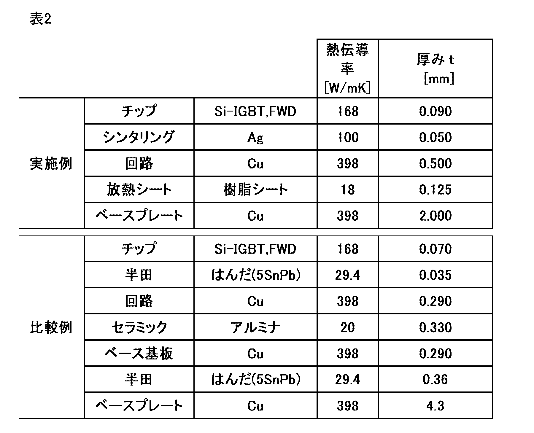
<Simulation conditions>
The outline of the simulation conditions is as follows.
FIGS. 3 to 5 and Table 2 show the physical property values and dimensions (thickness) of each component of the simulation example and the comparative example. FIG. 3A is a perspective view of the power module as viewed from above, and FIG. 3B is a plan view. FIG. 4A is a perspective view seen from the lower side of the power module, and FIG. 4B is a bottom view. FIG. 5 is a diagram showing thermal conditions in a simulation (heat transfer analysis).
Simulation software: ANSYS Mechanical 2019R3
Power semiconductor chip: Base substrate equipped with IGBT and FWD (Free Wheeling Diode): A convex pole is provided on the Cu base plate, and the back of the Cu base plate and the surface of the convex pole are cooled with cooling water (65 ° C).
シミュレーションの条件概要は次の通りである。
図3~5及び表2に、シミュレーションの実施例及び比較例の各構成要素の物性値・寸法(厚み)を示す。図3(a)はパワーモジュールの上側から見た斜視図、図3(b)が平面図である。図4(a)はパワーモジュールの下側から見た斜視図、図4(b)が底面図である。図5はシミュレーション(伝熱解析)における熱条件を示した図である。
シミュレーションソフト:ANSYS Mechanical 2019R3
パワー半導体チップ:IGBTとFWD(Free Wheeling Diode)を搭載した
ベース基板:Cuベース板に凸ポールを設け、Cuベース板裏及び凸ポール面を冷却水(65℃)で冷却した
The outline of the simulation conditions is as follows.
FIGS. 3 to 5 and Table 2 show the physical property values and dimensions (thickness) of each component of the simulation example and the comparative example. FIG. 3A is a perspective view of the power module as viewed from above, and FIG. 3B is a plan view. FIG. 4A is a perspective view seen from the lower side of the power module, and FIG. 4B is a bottom view. FIG. 5 is a diagram showing thermal conditions in a simulation (heat transfer analysis).
Simulation software: ANSYS Mechanical 2019R3
Power semiconductor chip: Base substrate equipped with IGBT and FWD (Free Wheeling Diode): A convex pole is provided on the Cu base plate, and the back of the Cu base plate and the surface of the convex pole are cooled with cooling water (65 ° C).
<シミュレーション結果>
図6に、シミュレーション結果として熱分布をパワーモジュールのモデル上に示す。
比較例では図6(a)に示すように、パワー半導体チップ(ここではIGBT)の表面の最大温度が184℃である。一方で、実施例では図6(b)に示すように、パワー半導体チップ(ここではIGBT)の表面の最大温度が152℃であり、比較例に対して32℃低い温度になった。 <Simulation result>
FIG. 6 shows the heat distribution on the model of the power module as a simulation result.
In the comparative example, as shown in FIG. 6A, the maximum temperature of the surface of the power semiconductor chip (here, the IGBT) is 184 ° C. On the other hand, in the example, as shown in FIG. 6B, the maximum temperature of the surface of the power semiconductor chip (here, the IGBT) was 152 ° C, which was 32 ° C lower than that of the comparative example.
<第3の実施例>
本実施例では、第1の熱抵抗R1、第2の熱抵抗R2及び比R1/R2に関するシミュレーションを行った。表3にシミュレーション結果を示す。 <Third Example>
In this embodiment, the simulation of the first thermal resistance R1, the second thermal resistance R2, and the ratio R1 / R2 was performed. Table 3 shows the simulation results.
本実施例では、第1の熱抵抗R1、第2の熱抵抗R2及び比R1/R2に関するシミュレーションを行った。表3にシミュレーション結果を示す。 <Third Example>
In this embodiment, the simulation of the first thermal resistance R1, the second thermal resistance R2, and the ratio R1 / R2 was performed. Table 3 shows the simulation results.
第1の熱抵抗R1に対応する実施形態の構成は、スペーサー30(下側半分)、パワー半導体チップ1(Si-IGBT)、第1接合層12(シンタリングペースト層)、第1Cu回路13、第1放熱シート14及び第1ヒートシンク15(Cu)を積層した構成である。本実施例では、第3接合層32を省いた構成でシミュレーションを行っている。
第2の熱抵抗R2に対応する実施形態の構成は、スペーサー30(上側半分)、第2接合層22(シンタリングペースト層)、第2Cu回路23、第2放熱シート24及び第2ヒートシンク25(Cu)を積層した構成である。 The configuration of the embodiment corresponding to the first thermal resistance R1 includes a spacer 30 (lower half), a power semiconductor chip 1 (Si-IGBT), a first bonding layer 12 (sintering paste layer), afirst Cu circuit 13, and the like. The first heat dissipation sheet 14 and the first heat sink 15 (Cu) are laminated. In this embodiment, the simulation is performed with a configuration in which the third bonding layer 32 is omitted.
The configuration of the embodiment corresponding to the second thermal resistance R2 includes a spacer 30 (upper half), a second bonding layer 22 (sintering paste layer), asecond Cu circuit 23, a second heat dissipation sheet 24, and a second heat sink 25 (the second heat sink 25 (upper half). It is a structure in which Cu) is laminated.
第2の熱抵抗R2に対応する実施形態の構成は、スペーサー30(上側半分)、第2接合層22(シンタリングペースト層)、第2Cu回路23、第2放熱シート24及び第2ヒートシンク25(Cu)を積層した構成である。 The configuration of the embodiment corresponding to the first thermal resistance R1 includes a spacer 30 (lower half), a power semiconductor chip 1 (Si-IGBT), a first bonding layer 12 (sintering paste layer), a
The configuration of the embodiment corresponding to the second thermal resistance R2 includes a spacer 30 (upper half), a second bonding layer 22 (sintering paste layer), a
各構成部材の熱伝導率及び厚み等は表に示した通りである。
このシミュレーション結果は以下の通りであった。
第1の熱抵抗R1=0.31[K/W]
第2の熱抵抗R2=0.30[K/W]
比R1/R2=1.023 The thermal conductivity, thickness, etc. of each component are as shown in the table.
The results of this simulation are as follows.
First thermal resistance R1 = 0.31 [K / W]
Second thermal resistance R2 = 0.30 [K / W]
Ratio R1 / R2 = 1.023
すなわち、第1の熱抵抗R1及び第2の熱抵抗R2が0.05(K/W)以上0.5(K/W)以下の範囲であった。比R1/R2が0.7以上1.3以下であった。
That is, the first thermal resistance R1 and the second thermal resistance R2 were in the range of 0.05 (K / W) or more and 0.5 (K / W) or less. The ratio R1 / R2 was 0.7 or more and 1.3 or less.
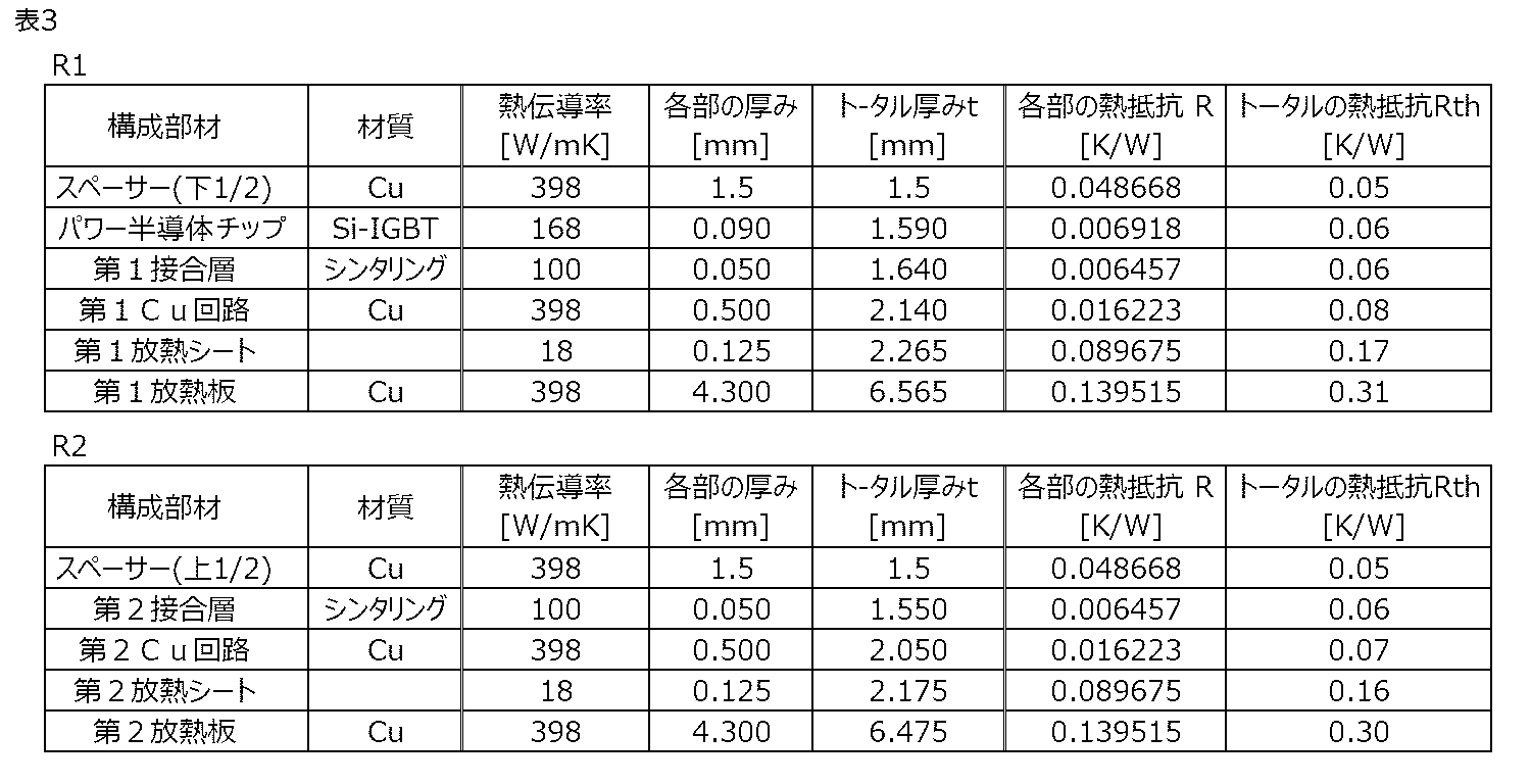
この出願は、2020年7月21日に出願された日本出願特願2020-124566号および2021年1月26日に出願された日本出願特願2021-010158号を基礎とする優先権を主張し、その開示の全てをここに取り込む。
This application claims priority on the basis of Japanese Application Japanese Patent Application No. 2020-124566 filed on July 21, 2020 and Japanese Application Japanese Patent Application No. 2021-01158 filed on January 26, 2021. , All of its disclosures are taken here.
1 パワー半導体チップ(パワー半導体素子)
2 シンタリング層(第1接合層)
3 Cu回路(第1金属回路基板)
4 放熱シート(第1放熱シート)
5 Cuベースプレート(第1放熱部材)
6 リードフレーム
7 封止材
10、100 パワーモジュール
12 第1接合層
13 第1Cu回路(第1金属回路基板)
14 第1放熱シート
15 第1ヒートシンク(第1放熱部材)
22 第2接合層
23 第2Cu回路(第2金属回路基板)
24 第2放熱シート
25 第2ヒートシンク(第2放熱部材)
30 スペーサー
30C スペーサー中心
32 第3接合層
50 封止材層
60 第1放熱構造
70 第2放熱構造
100 パワーモジュール 1 Power semiconductor chip (power semiconductor element)
2 Sintering layer (first bonding layer)
3 Cu circuit (first metal circuit board)
4 Heat dissipation sheet (first heat dissipation sheet)
5 Cu base plate (first heat dissipation member)
6 Leadframe 7 Encapsulant 10, 100 Power module 12 First junction layer 13 First Cu circuit (first metal circuit board)
14 1stheat dissipation sheet 15 1st heat sink (1st heat dissipation member)
22Second junction layer 23 Second Cu circuit (second metal circuit board)
24 Secondheat dissipation sheet 25 Second heat sink (second heat dissipation member)
30Spacer 30C Spacer center 32 Third bonding layer
50Encapsulant layer 60 First heat dissipation structure 70 Second heat dissipation structure 100 Power module
2 シンタリング層(第1接合層)
3 Cu回路(第1金属回路基板)
4 放熱シート(第1放熱シート)
5 Cuベースプレート(第1放熱部材)
6 リードフレーム
7 封止材
10、100 パワーモジュール
12 第1接合層
13 第1Cu回路(第1金属回路基板)
14 第1放熱シート
15 第1ヒートシンク(第1放熱部材)
22 第2接合層
23 第2Cu回路(第2金属回路基板)
24 第2放熱シート
25 第2ヒートシンク(第2放熱部材)
30 スペーサー
30C スペーサー中心
32 第3接合層
50 封止材層
60 第1放熱構造
70 第2放熱構造
100 パワーモジュール 1 Power semiconductor chip (power semiconductor element)
2 Sintering layer (first bonding layer)
3 Cu circuit (first metal circuit board)
4 Heat dissipation sheet (first heat dissipation sheet)
5 Cu base plate (first heat dissipation member)
6 Lead
14 1st
22
24 Second
30
50
Claims (15)
- パワー半導体素子と、
前記パワー半導体素子を一方の面側に設けた第1放熱構造と、
を有し、
前記第1放熱構造は、
第1金属回路基板と、
前記パワー半導体素子を前記第1金属回路基板の一方の面にシンタリングペーストにより接合するために設けた第1接合層と、
前記第1金属回路基板の他方の面に第1放熱部材を接合するために設けた第1放熱シートと、
を有し、
前記パワー半導体素子と、前記第1接合層と、前記第1金属回路基板と、前記第1放熱シートとが積層された積層構造Aにおいて、積層方向の熱抵抗の合計が0.30(K/W)以下である、
パワーモジュール。 Power semiconductor devices and
A first heat dissipation structure in which the power semiconductor element is provided on one side,
Have,
The first heat dissipation structure is
The first metal circuit board and
A first bonding layer provided for bonding the power semiconductor element to one surface of the first metal circuit board with a sintering paste,
A first heat dissipation sheet provided for joining the first heat dissipation member to the other surface of the first metal circuit board, and
Have,
In the laminated structure A in which the power semiconductor element, the first junction layer, the first metal circuit board, and the first heat dissipation sheet are laminated, the total thermal resistance in the lamination direction is 0.30 (K /). W) Below,
Power module. - 前記第1放熱構造は、
前記第1金属回路基板の他方の面に前記第1放熱シートにより接合された第1放熱部材を更に有する、請求項1に記載のパワーモジュール。 The first heat dissipation structure is
The power module according to claim 1, further comprising a first heat radiating member bonded to the other surface of the first metal circuit board by the first heat radiating sheet. - 前記パワー半導体素子と、前記第1接合層と、前記第1金属回路基板と、前記第1放熱シートと、前記第1放熱部材とが積層された積層構造Bにおいて、積層方向(高さ方向)の熱抵抗の合計が0.45(K/W)以下である、請求項2に記載のパワーモジュール。 In the laminated structure B in which the power semiconductor element, the first bonding layer, the first metal circuit board, the first heat radiating sheet, and the first heat radiating member are laminated, the stacking direction (height direction). The power module according to claim 2, wherein the total thermal resistance of the above is 0.45 (K / W) or less.
- 前記積層構造Aの前記積層方向の熱抵抗の合計をXA(W/K)、前記積層構造Aの厚みの合計をtA(mm)とした場合に、比XA/tAが0.25(W/(K・mm))以下である、請求項1から3までのいずれか1項に記載のパワーモジュール。 When the total thermal resistance of the laminated structure A in the laminated direction is XA (W / K) and the total thickness of the laminated structure A is tA (mm), the ratio XA / tA is 0.25 (W / K). (K · mm)) The power module according to any one of claims 1 to 3, which is as follows.
- 前記積層構造Bの前記積層方向の熱抵抗の合計をXB(W/K)、前記積層構造Bの厚みの合計をtB(mm)とした場合に、比XB/tBが0.08(W/(K・mm))以下である、請求項3に記載のパワーモジュール。 When the total thermal resistance of the laminated structure B in the laminated direction is XB (W / K) and the total thickness of the laminated structure B is tB (mm), the ratio XB / tB is 0.08 (W / K). (K · mm)) The power module according to claim 3, wherein the power module is as follows.
- 前記パワー半導体素子の他方の面側に設けた第2放熱構造と、前記パワー半導体素子と前記第2放熱構造との間に設けたスペーサーと、
を更に有し、
前記第2放熱構造は、第2金属回路基板と、前記第2金属回路基板の一方の面に前記スペーサーをシンタリングペーストにより接合するために設けた第2接合層と、
を有し、
前記パワー半導体素子と前記スペーサーとをシンタリングペーストにより接合する第3接合層と、
前記第1放熱構造と前記第2放熱構造との間の領域において、前記パワー半導体素子、前記スペーサー及び前記第1~第3接合層が設けられていない領域をモールド封止材により封止した封止材層と、
を有する、請求項1から6までのいずれか1項に記載のパワーモジュール。 A second heat dissipation structure provided on the other surface side of the power semiconductor element, and a spacer provided between the power semiconductor element and the second heat dissipation structure.
Further have
The second heat dissipation structure includes a second metal circuit board and a second bonding layer provided for bonding the spacer to one surface of the second metal circuit board with a sintering paste.
Have,
A third bonding layer for bonding the power semiconductor element and the spacer with a sintering paste,
In the region between the first heat dissipation structure and the second heat dissipation structure, the region where the power semiconductor element, the spacer, and the first to third bonding layers are not provided is sealed with a mold encapsulant. With the stop material layer,
The power module according to any one of claims 1 to 6. - 前記第2放熱構造は、
前記第2金属回路基板の他方の面に第2放熱部材を接合するために設けられた第2放熱シートを更に有する、
を有する、請求項6に記載のパワーモジュール。 The second heat dissipation structure is
Further having a second heat radiating sheet provided for joining the second heat radiating member to the other surface of the second metal circuit board.
The power module according to claim 6. - 前記第2放熱構造は、
前記第2金属回路基板の他方の面に前記第2放熱シートにより接合された第2放熱部材を更に有する、請求項7に記載のパワーモジュール。 The second heat dissipation structure is
The power module according to claim 7, further comprising a second heat radiating member bonded to the other surface of the second metal circuit board by the second heat radiating sheet. - 前記スペーサーの厚さ方向中心から前記第1放熱構造までの積層方向の第1の熱抵抗R1と、前記スペーサーの厚さ方向中心から前記第2放熱構造までの積層方向の第2の熱抵抗R2との比R1/R2が0.7以上1.3以下である、請求項6から8までのいずれか1項に記載のパワーモジュール。 The first thermal resistance R1 in the stacking direction from the center in the thickness direction of the spacer to the first heat dissipation structure, and the second thermal resistance R2 in the stacking direction from the center in the thickness direction of the spacer to the second heat dissipation structure. The power module according to any one of claims 6 to 8, wherein the ratio R1 / R2 to and R2 is 0.7 or more and 1.3 or less.
- 前記第1の熱抵抗R1及び前記第2の熱抵抗R2は0.05(K/W)以上0.5(K/W)以下である、請求項9に記載のパワーモジュール。 The power module according to claim 9, wherein the first thermal resistance R1 and the second thermal resistance R2 are 0.05 (K / W) or more and 0.5 (K / W) or less.
- 前記シンタリングペーストに含有される金属粒子は、銀粒子、アルミニウム粒子または銅粒子のいずれかである、請求項1から10までのいずれか1項に記載のパワーモジュール。 The power module according to any one of claims 1 to 10, wherein the metal particles contained in the sintering paste are either silver particles, aluminum particles or copper particles.
- 前記パワー半導体素子を覆う封止材をさらに備える、請求項1から11までのいずれか1項に記載のパワーモジュール。 The power module according to any one of claims 1 to 11, further comprising a sealing material for covering the power semiconductor element.
- 前記封止材はモールド樹脂からなる、請求項12に記載のパワーモジュール。 The power module according to claim 12, wherein the sealing material is made of a mold resin.
- 前記封止材は、前記第1放熱部材および/または第2放熱部材の厚さ方向の側面の一部又は全部を覆うように前記パワー半導体素子を覆って封止している請求項12または13に記載のパワーモジュール。 12. The power module described in.
- 前記第1金属回路基板および/または第2金属回路基板は厚銅(圧延銅)をパターンニングした回路基板であって、厚みが0.3mm以上5mm以下である、請求項1から14までのいずれか1項に記載のパワーモジュール。 The first metal circuit board and / or the second metal circuit board is a circuit board in which thick copper (rolled copper) is patterned, and the thickness is 0.3 mm or more and 5 mm or less, any of claims 1 to 14. Or the power module described in item 1.
Priority Applications (4)
| Application Number | Priority Date | Filing Date | Title |
|---|---|---|---|
| EP21846068.1A EP4187590A1 (en) | 2020-07-21 | 2021-07-02 | Power module |
| CN202180061197.8A CN116195050A (en) | 2020-07-21 | 2021-07-02 | Power module |
| US18/016,122 US20230298962A1 (en) | 2020-07-21 | 2021-07-02 | Power module |
| KR1020237005463A KR20230039710A (en) | 2020-07-21 | 2021-07-02 | power module |
Applications Claiming Priority (4)
| Application Number | Priority Date | Filing Date | Title |
|---|---|---|---|
| JP2020124566A JP2022021143A (en) | 2020-07-21 | 2020-07-21 | Power module |
| JP2020-124566 | 2020-07-21 | ||
| JP2021-010158 | 2021-01-26 | ||
| JP2021010158A JP2022114048A (en) | 2021-01-26 | 2021-01-26 | power module |
Publications (1)
| Publication Number | Publication Date |
|---|---|
| WO2022019089A1 true WO2022019089A1 (en) | 2022-01-27 |
Family
ID=79729723
Family Applications (1)
| Application Number | Title | Priority Date | Filing Date |
|---|---|---|---|
| PCT/JP2021/025107 WO2022019089A1 (en) | 2020-07-21 | 2021-07-02 | Power module |
Country Status (5)
| Country | Link |
|---|---|
| US (1) | US20230298962A1 (en) |
| EP (1) | EP4187590A1 (en) |
| KR (1) | KR20230039710A (en) |
| CN (1) | CN116195050A (en) |
| WO (1) | WO2022019089A1 (en) |
Cited By (1)
| Publication number | Priority date | Publication date | Assignee | Title |
|---|---|---|---|---|
| WO2024076880A1 (en) * | 2022-10-05 | 2024-04-11 | Semiconductor Components Industries, Llc | Integrated substrates and related methods |
Citations (9)
| Publication number | Priority date | Publication date | Assignee | Title |
|---|---|---|---|---|
| JP2010010504A (en) * | 2008-06-30 | 2010-01-14 | Hitachi Ltd | Power semiconductor module |
| JP2012028421A (en) | 2010-07-20 | 2012-02-09 | Nhk Spring Co Ltd | Laminate sheet for circuit board integrating heat sink with fin, circuit board integrating heat sink with fin and method of manufacturing laminate sheet for circuit board integrating heat sink with fin |
| JP2014022579A (en) * | 2012-07-19 | 2014-02-03 | Rohm Co Ltd | Power module semiconductor device |
| WO2017138402A1 (en) * | 2016-02-08 | 2017-08-17 | ローム株式会社 | Semiconductor device, power module, method for manufacturing semiconductor device and method for manufacturing power module |
| JP2019062122A (en) * | 2017-09-27 | 2019-04-18 | 株式会社デンソー | Package mounting body |
| JP2019071399A (en) * | 2016-11-21 | 2019-05-09 | ローム株式会社 | Power module and manufacturing method thereof, graphite plate, and power supply |
| JP2020027878A (en) * | 2018-08-10 | 2020-02-20 | 株式会社豊田中央研究所 | Semiconductor device |
| JP2020124566A (en) | 2013-08-30 | 2020-08-20 | キャプニア, インク.Capnia, Inc. | Neonatal carbon dioxide measurement system |
| JP2021010158A (en) | 2019-06-28 | 2021-01-28 | キヤノン株式会社 | Imaging display device and wearable device |
-
2021
- 2021-07-02 US US18/016,122 patent/US20230298962A1/en active Pending
- 2021-07-02 CN CN202180061197.8A patent/CN116195050A/en active Pending
- 2021-07-02 EP EP21846068.1A patent/EP4187590A1/en active Pending
- 2021-07-02 KR KR1020237005463A patent/KR20230039710A/en unknown
- 2021-07-02 WO PCT/JP2021/025107 patent/WO2022019089A1/en unknown
Patent Citations (9)
| Publication number | Priority date | Publication date | Assignee | Title |
|---|---|---|---|---|
| JP2010010504A (en) * | 2008-06-30 | 2010-01-14 | Hitachi Ltd | Power semiconductor module |
| JP2012028421A (en) | 2010-07-20 | 2012-02-09 | Nhk Spring Co Ltd | Laminate sheet for circuit board integrating heat sink with fin, circuit board integrating heat sink with fin and method of manufacturing laminate sheet for circuit board integrating heat sink with fin |
| JP2014022579A (en) * | 2012-07-19 | 2014-02-03 | Rohm Co Ltd | Power module semiconductor device |
| JP2020124566A (en) | 2013-08-30 | 2020-08-20 | キャプニア, インク.Capnia, Inc. | Neonatal carbon dioxide measurement system |
| WO2017138402A1 (en) * | 2016-02-08 | 2017-08-17 | ローム株式会社 | Semiconductor device, power module, method for manufacturing semiconductor device and method for manufacturing power module |
| JP2019071399A (en) * | 2016-11-21 | 2019-05-09 | ローム株式会社 | Power module and manufacturing method thereof, graphite plate, and power supply |
| JP2019062122A (en) * | 2017-09-27 | 2019-04-18 | 株式会社デンソー | Package mounting body |
| JP2020027878A (en) * | 2018-08-10 | 2020-02-20 | 株式会社豊田中央研究所 | Semiconductor device |
| JP2021010158A (en) | 2019-06-28 | 2021-01-28 | キヤノン株式会社 | Imaging display device and wearable device |
Cited By (1)
| Publication number | Priority date | Publication date | Assignee | Title |
|---|---|---|---|---|
| WO2024076880A1 (en) * | 2022-10-05 | 2024-04-11 | Semiconductor Components Industries, Llc | Integrated substrates and related methods |
Also Published As
| Publication number | Publication date |
|---|---|
| CN116195050A (en) | 2023-05-30 |
| KR20230039710A (en) | 2023-03-21 |
| EP4187590A1 (en) | 2023-05-31 |
| US20230298962A1 (en) | 2023-09-21 |
Similar Documents
| Publication | Publication Date | Title |
|---|---|---|
| JP6402763B2 (en) | Multilayer resin sheet, resin sheet laminate, cured multilayer resin sheet and method for producing the same, multilayer resin sheet with metal foil, and semiconductor device | |
| US8007897B2 (en) | Insulating sheet and method for producing it, and power module comprising the insulating sheet | |
| WO2017014238A1 (en) | Thermoconductive resin composition, thermoconductive sheet, and semiconductor device | |
| JP6627303B2 (en) | Thermal conductive resin composition, laminate for circuit board, circuit board and semiconductor device | |
| WO2015163054A1 (en) | Metal-based substrate, method for manufacturing metal-based substrate, metal-based circuit board, and electronic device | |
| JP2016004841A (en) | Metal foil-clad board, circuit board and heating element mounting board | |
| JP5391530B2 (en) | Method for manufacturing thermally conductive resin sheet and method for manufacturing power module | |
| KR102377281B1 (en) | Method of manufacturing semiconductor device | |
| WO2022019089A1 (en) | Power module | |
| JP6508384B2 (en) | Thermal conductive sheet and semiconductor device | |
| JP2022123984A (en) | Manufacturing method for circuit board | |
| JPWO2020137989A1 (en) | A resin composition for encapsulation, a semiconductor device, and a method for manufacturing the semiconductor device. | |
| JP7200674B2 (en) | Manufacturing method of heat dissipation structure | |
| JP2022021143A (en) | Power module | |
| JP2022098698A (en) | Resin composition and power module | |
| JP2022114048A (en) | power module | |
| WO2017014237A1 (en) | Substrate for power modules, circuit board for power modules, and power module | |
| JP2022000486A (en) | Epoxy resin, thermosetting resin composition, and method for producing epoxy resin | |
| WO2016002892A1 (en) | Heat-conductive sheet and semiconductor device | |
| JP2017028130A (en) | Substrate for power module, circuit board for power module, and power module | |
| JP2023118508A (en) | power module | |
| WO2022255450A1 (en) | Resin sheet, laminate, and semiconductor device | |
| WO2023090013A1 (en) | Heat-sink-equipped circuit board, method for manufacturing same, semiconductor device, and method for manufacturing same | |
| JP2023107225A (en) | Laminate and semiconductor device | |
| JP2021195452A (en) | Phenolic compound, phenolic curative, thermosetting resin composition, and phenolic compound production method |
Legal Events
| Date | Code | Title | Description |
|---|---|---|---|
| 121 | Ep: the epo has been informed by wipo that ep was designated in this application |
Ref document number: 21846068 Country of ref document: EP Kind code of ref document: A1 |
|
| ENP | Entry into the national phase |
Ref document number: 20237005463 Country of ref document: KR Kind code of ref document: A |
|
| NENP | Non-entry into the national phase |
Ref country code: DE |
|
| ENP | Entry into the national phase |
Ref document number: 2021846068 Country of ref document: EP Effective date: 20230221 |