WO2022014382A1 - レーザ加工装置、ウェーハ加工システム及びレーザ加工装置の制御方法 - Google Patents
レーザ加工装置、ウェーハ加工システム及びレーザ加工装置の制御方法 Download PDFInfo
- Publication number
- WO2022014382A1 WO2022014382A1 PCT/JP2021/025179 JP2021025179W WO2022014382A1 WO 2022014382 A1 WO2022014382 A1 WO 2022014382A1 JP 2021025179 W JP2021025179 W JP 2021025179W WO 2022014382 A1 WO2022014382 A1 WO 2022014382A1
- Authority
- WO
- WIPO (PCT)
- Prior art keywords
- processing
- laser
- machining
- groove
- street
- Prior art date
- Legal status (The legal status is an assumption and is not a legal conclusion. Google has not performed a legal analysis and makes no representation as to the accuracy of the status listed.)
- Ceased
Links
Images








Classifications
-
- B—PERFORMING OPERATIONS; TRANSPORTING
- B23—MACHINE TOOLS; METAL-WORKING NOT OTHERWISE PROVIDED FOR
- B23K—SOLDERING OR UNSOLDERING; WELDING; CLADDING OR PLATING BY SOLDERING OR WELDING; CUTTING BY APPLYING HEAT LOCALLY, e.g. FLAME CUTTING; WORKING BY LASER BEAM
- B23K26/00—Working by laser beam, e.g. welding, cutting or boring
- B23K26/36—Removing material
- B23K26/362—Laser etching
- B23K26/364—Laser etching for making a groove or trench, e.g. for scribing a break initiation groove
-
- B—PERFORMING OPERATIONS; TRANSPORTING
- B23—MACHINE TOOLS; METAL-WORKING NOT OTHERWISE PROVIDED FOR
- B23K—SOLDERING OR UNSOLDERING; WELDING; CLADDING OR PLATING BY SOLDERING OR WELDING; CUTTING BY APPLYING HEAT LOCALLY, e.g. FLAME CUTTING; WORKING BY LASER BEAM
- B23K26/00—Working by laser beam, e.g. welding, cutting or boring
- B23K26/02—Positioning or observing the workpiece, e.g. with respect to the point of impact; Aligning, aiming or focusing the laser beam
- B23K26/03—Observing, e.g. monitoring, the workpiece
-
- B—PERFORMING OPERATIONS; TRANSPORTING
- B23—MACHINE TOOLS; METAL-WORKING NOT OTHERWISE PROVIDED FOR
- B23K—SOLDERING OR UNSOLDERING; WELDING; CLADDING OR PLATING BY SOLDERING OR WELDING; CUTTING BY APPLYING HEAT LOCALLY, e.g. FLAME CUTTING; WORKING BY LASER BEAM
- B23K26/00—Working by laser beam, e.g. welding, cutting or boring
- B23K26/02—Positioning or observing the workpiece, e.g. with respect to the point of impact; Aligning, aiming or focusing the laser beam
- B23K26/03—Observing, e.g. monitoring, the workpiece
- B23K26/032—Observing, e.g. monitoring, the workpiece using optical means
-
- B—PERFORMING OPERATIONS; TRANSPORTING
- B23—MACHINE TOOLS; METAL-WORKING NOT OTHERWISE PROVIDED FOR
- B23K—SOLDERING OR UNSOLDERING; WELDING; CLADDING OR PLATING BY SOLDERING OR WELDING; CUTTING BY APPLYING HEAT LOCALLY, e.g. FLAME CUTTING; WORKING BY LASER BEAM
- B23K26/00—Working by laser beam, e.g. welding, cutting or boring
- B23K26/02—Positioning or observing the workpiece, e.g. with respect to the point of impact; Aligning, aiming or focusing the laser beam
- B23K26/06—Shaping the laser beam, e.g. by masks or multi-focusing
- B23K26/062—Shaping the laser beam, e.g. by masks or multi-focusing by direct control of the laser beam
- B23K26/0622—Shaping the laser beam, e.g. by masks or multi-focusing by direct control of the laser beam by shaping pulses
-
- B—PERFORMING OPERATIONS; TRANSPORTING
- B23—MACHINE TOOLS; METAL-WORKING NOT OTHERWISE PROVIDED FOR
- B23K—SOLDERING OR UNSOLDERING; WELDING; CLADDING OR PLATING BY SOLDERING OR WELDING; CUTTING BY APPLYING HEAT LOCALLY, e.g. FLAME CUTTING; WORKING BY LASER BEAM
- B23K26/00—Working by laser beam, e.g. welding, cutting or boring
- B23K26/08—Devices involving relative movement between laser beam and workpiece
- B23K26/0823—Devices involving rotation of the workpiece
-
- B—PERFORMING OPERATIONS; TRANSPORTING
- B23—MACHINE TOOLS; METAL-WORKING NOT OTHERWISE PROVIDED FOR
- B23K—SOLDERING OR UNSOLDERING; WELDING; CLADDING OR PLATING BY SOLDERING OR WELDING; CUTTING BY APPLYING HEAT LOCALLY, e.g. FLAME CUTTING; WORKING BY LASER BEAM
- B23K26/00—Working by laser beam, e.g. welding, cutting or boring
- B23K26/08—Devices involving relative movement between laser beam and workpiece
- B23K26/083—Devices involving movement of the workpiece in at least one axial direction
- B23K26/0853—Devices involving movement of the workpiece in at least two axial directions, e.g. in a plane
- B23K26/0861—Devices involving movement of the workpiece in at least two axial directions, e.g. in a plane in at least three axial directions
-
- B—PERFORMING OPERATIONS; TRANSPORTING
- B23—MACHINE TOOLS; METAL-WORKING NOT OTHERWISE PROVIDED FOR
- B23K—SOLDERING OR UNSOLDERING; WELDING; CLADDING OR PLATING BY SOLDERING OR WELDING; CUTTING BY APPLYING HEAT LOCALLY, e.g. FLAME CUTTING; WORKING BY LASER BEAM
- B23K26/00—Working by laser beam, e.g. welding, cutting or boring
- B23K26/36—Removing material
- B23K26/40—Removing material taking account of the properties of the material involved
- B23K26/402—Removing material taking account of the properties of the material involved involving non-metallic material, e.g. isolators
-
- B—PERFORMING OPERATIONS; TRANSPORTING
- B23—MACHINE TOOLS; METAL-WORKING NOT OTHERWISE PROVIDED FOR
- B23K—SOLDERING OR UNSOLDERING; WELDING; CLADDING OR PLATING BY SOLDERING OR WELDING; CUTTING BY APPLYING HEAT LOCALLY, e.g. FLAME CUTTING; WORKING BY LASER BEAM
- B23K26/00—Working by laser beam, e.g. welding, cutting or boring
- B23K26/70—Auxiliary operations or equipment
- B23K26/702—Auxiliary equipment
-
- B—PERFORMING OPERATIONS; TRANSPORTING
- B23—MACHINE TOOLS; METAL-WORKING NOT OTHERWISE PROVIDED FOR
- B23K—SOLDERING OR UNSOLDERING; WELDING; CLADDING OR PLATING BY SOLDERING OR WELDING; CUTTING BY APPLYING HEAT LOCALLY, e.g. FLAME CUTTING; WORKING BY LASER BEAM
- B23K26/00—Working by laser beam, e.g. welding, cutting or boring
- B23K26/70—Auxiliary operations or equipment
- B23K26/702—Auxiliary equipment
- B23K26/705—Beam measuring devices
-
- H—ELECTRICITY
- H10—SEMICONDUCTOR DEVICES; ELECTRIC SOLID-STATE DEVICES NOT OTHERWISE PROVIDED FOR
- H10P—GENERIC PROCESSES OR APPARATUS FOR THE MANUFACTURE OR TREATMENT OF DEVICES COVERED BY CLASS H10
- H10P72/00—Handling or holding of wafers, substrates or devices during manufacture or treatment thereof
- H10P72/04—Apparatus for manufacture or treatment
- H10P72/0428—Apparatus for mechanical treatment or grinding or cutting
-
- H—ELECTRICITY
- H10—SEMICONDUCTOR DEVICES; ELECTRIC SOLID-STATE DEVICES NOT OTHERWISE PROVIDED FOR
- H10P—GENERIC PROCESSES OR APPARATUS FOR THE MANUFACTURE OR TREATMENT OF DEVICES COVERED BY CLASS H10
- H10P95/00—Generic processes or apparatus for manufacture or treatments not covered by the other groups of this subclass
-
- B—PERFORMING OPERATIONS; TRANSPORTING
- B23—MACHINE TOOLS; METAL-WORKING NOT OTHERWISE PROVIDED FOR
- B23K—SOLDERING OR UNSOLDERING; WELDING; CLADDING OR PLATING BY SOLDERING OR WELDING; CUTTING BY APPLYING HEAT LOCALLY, e.g. FLAME CUTTING; WORKING BY LASER BEAM
- B23K2101/00—Articles made by soldering, welding or cutting
- B23K2101/36—Electric or electronic devices
- B23K2101/40—Semiconductor devices
-
- B—PERFORMING OPERATIONS; TRANSPORTING
- B23—MACHINE TOOLS; METAL-WORKING NOT OTHERWISE PROVIDED FOR
- B23K—SOLDERING OR UNSOLDERING; WELDING; CLADDING OR PLATING BY SOLDERING OR WELDING; CUTTING BY APPLYING HEAT LOCALLY, e.g. FLAME CUTTING; WORKING BY LASER BEAM
- B23K2103/00—Materials to be soldered, welded or cut
- B23K2103/50—Inorganic materials other than metals or composite materials
Definitions
- the present invention relates to a laser processing apparatus for laser processing a wafer, a wafer processing system, and a control method for the laser processing apparatus.
- a plurality of devices are formed by laminating a low-dielectric-constant insulator film (Low-k film) made of a glassy material and a functional film forming a circuit on the surface of a substrate such as silicon.
- Wafers semiconductor wafers
- a plurality of devices are partitioned in a grid pattern by grid-like streets, and individual devices are manufactured by dividing the wafer along the streets.
- Patent Document 1 and Patent Document 2 the laser optical system is relatively moved along the street in the processing feed direction with respect to the wafer, and the laser beam is irradiated from the laser optical system to the street along the street.
- a laser processing apparatus for forming a processing groove is disclosed. According to this laser processing apparatus, it is possible to remove a Low-k film or the like from the street by forming a processing groove along the street.
- the present invention has been made in view of such circumstances, and an object of the present invention is to provide a laser processing apparatus, a wafer processing system, and a control method of a laser processing apparatus capable of confirming a processing state of a processing groove in real time.
- the laser processing apparatus for achieving the object of the present invention is a street by irradiating the street with laser light from the laser optical system while moving the laser optical system relative to the wafer in the processing feed direction along the street of the wafer.
- a laser processing device that forms a processing groove along the
- the brightness detection unit that detects the brightness of the plasma generated at the processing point by the irradiation of the laser light based on the observation image, the brightness, the energy of the laser light, and the processing state of the processing groove.
- the processing state is determined by referring to the correspondence information based on the brightness and the known energy of the laser beam. It is equipped with a processing state determination unit.
- this laser processing device it is possible to determine the processing state of laser processing for each processing point in real time based on the detection result of the plasma brightness at each processing point.
- the observation image acquisition unit includes an optical element that blocks light in the wavelength range of the laser light and an observation optical system that captures a processing point through the optical element.
- the corresponding information acquisition unit indicates the correspondence between the luminance, the energy of the laser beam, and the processing state including the depth of the processing groove and the temperature of the processing point. Get information. This makes it possible to determine the machining state (depth of the machining groove and the temperature of the machining point) of laser machining for each machining point in real time.
- the laser optical system differs in at least one of the depth position of the processing point from the surface of the wafer and the amount of removed matter generated by the formation of the processing groove. It is possible to selectively form a machining groove under multiple machining conditions, and it is equipped with a machining condition selection unit that selects machining conditions, and the corresponding information acquisition unit processes from a plurality of corresponding information corresponding to multiple machining conditions. Acquires the correspondence information corresponding to the machining condition selected by the condition selection unit. As a result, the machining state of the machined groove can be discriminated for each machining condition, so that the machining state of the machined groove can be discriminated more accurately.
- the correspondence information acquisition unit acquires a plurality of correspondence information corresponding to the material for each region.
- a position information acquisition unit that acquires the position information of the processing point is provided, and the processing state determination unit uses the position information acquired by the position information acquisition unit and the known wafer design information as the material at the position of the processing point.
- the machining state is determined using the corresponding correspondence information.
- the energy of the laser light emitted by the laser optical system is controlled based on the discrimination result of the machining state discriminating unit for machining. It is equipped with a laser machining control unit that maintains a constant state. Thereby, the processing quality of the processing groove can be improved.
- the wafer processing system for achieving the object of the present invention includes the above-mentioned laser processing apparatus and a server having a storage unit for storing correspondence information, and the correspondence information acquisition unit acquires correspondence information from the storage unit. ..
- At least one laser processing apparatus acquires a groove shape including at least the depth of the processing groove formed at the processing point for each processing point along the street.
- the server includes a shape acquisition unit, an actual measurement information output unit that outputs actual measurement information of the brightness and groove shape for each machining point to the server based on the detection result of the brightness detection unit and the acquisition result of the groove shape acquisition unit.
- a correspondence information generation unit is provided which generates correspondence information and stores it in a storage unit based on the actual measurement information output from the actual measurement information output unit.
- the control method of the laser processing apparatus for achieving the object of the present invention is to irradiate the street with laser light from the laser optical system while moving the laser optical system relative to the wafer in the processing feed direction along the street of the wafer.
- the observation image acquisition step of repeatedly acquiring the observation image of the processing point of the laser beam emitted from the laser optical system to the street during the formation of the processing groove.
- the brightness detection step that detects the brightness of the plasma generated at the processing point by the irradiation of the laser beam based on the observation image, the brightness, and the energy of the laser beam.
- the correspondence information acquisition step for acquiring the correspondence information indicating the correspondence relationship between the machining state of the machined groove and the brightness detection step
- the correspondence information is referred to based on the brightness and the known laser beam energy. It has a machining state determination step for determining the machining state.
- the machined state of the machined groove can be confirmed in real time.
- FIG. 1 is a schematic view of the laser processing apparatus 10 of the first embodiment.
- the laser processing apparatus 10 laser-processes a wafer W (for example, a silicon wafer) as a pre-process of a cutting process for dividing a wafer W (for example, a silicon wafer) into a plurality of chips 4 (see FIG. 2). Processing).
- the XYZ directions in the figure are orthogonal to each other, of which the X and Y directions are horizontal, and the Z direction is the vertical direction (thickness direction of the wafer W).
- the ⁇ direction is a rotation direction with the Z direction as the rotation axis.
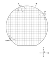
- FIG. 2 is a plan view of the wafer W to be machined by the laser machining apparatus 10.
- the wafer W is a laminated body in which a Low-k film and a functional film forming a circuit are laminated on the surface of a substrate such as silicon.
- the wafer W is divided into a plurality of regions by a plurality of street channels (also referred to as planned division lines) arranged in a grid pattern.
- a chip 4 (device) is provided in each of the partitioned areas.
- the laser processing apparatus 10 performs laser processing along the street CH for each street CH to remove the Low-k film and the like on the street CH to form a processing groove 9 (also referred to as an ablation groove or a laser groove). ..
- the laser machining apparatus 10 includes a base 12, an XYZ ⁇ stage 14, an adsorption stage 16, a machining unit 18, a monitor 20, and a control device 22.
- An XYZ ⁇ stage 14 is provided on the base 12.
- the XYZ ⁇ stage 14 is provided on the base 12 so as to be movable in the XYZ direction and rotatably in the ⁇ direction.
- the XYZ ⁇ stage 14 is moved in the XYZ direction and rotated in the ⁇ direction by a moving mechanism 24 (see FIG. 3) composed of an actuator, a motor, and the like.
- the adsorption stage 16 is provided on the XYZ ⁇ stage 14.
- the suction stage 16 sucks and holds the back surface of the wafer W.
- the wafer W is held in the XYZ ⁇ stage 14 so that the surface on the side on which the above-mentioned Low-k film or the like is formed faces the processing unit 18 described later.
- the machining unit 18 is relatively moved in the XYZ ⁇ direction with respect to the wafer W on the suction stage 16.
- the processing unit 18 includes a laser optical system 25 and an observation optical system 30.
- the processing unit 18 is arranged at a position on the upper side of the suction stage 16 in the Z direction (position facing the wafer W), and is controlled by a control device 22 described later.
- the laser optical system 25 irradiates the laser beam L toward the street CH of the wafer W.
- the laser optical system 25 includes a laser light source 26 (laser oscillator), a collimating lens 27, a half mirror 28, and a condenser lens 29 (condensation lens).
- the laser light source 26 emits a laser beam L (for example, a pulsed laser beam) toward the collimating lens 27.
- the conditions of the laser beam L are, for example, a light source: UV (ultraviolet) -pulse laser, a wavelength: 400 nm or less, a repetition frequency of 1 to 100 kHz, and an average output of 0.5 to 10 watts, but are particularly limited to these conditions. It is not something that will be done.
- the collimating lens 27 converts the laser beam L incident from the laser light source 26 into a parallel light flux, and then emits the laser beam L toward the half mirror 28.
- the half mirror 28 is arranged on the optical axis of the condenser lens 29, and reflects a part of the laser beam L incident from the collimating lens 27 toward the condenser lens 29. Further, the half mirror 28 transmits a part of the illumination light IL described later incident from the half mirror 33 described later and emits the light toward the condenser lens 29, and reflects the illumination light IL incident from the condenser lens 29. A part of the light is transmitted and emitted toward the half mirror 33.
- the condensing lens 29 condenses the laser beam L and the illumination light IL incident from the half mirror 28 on the street CH of the wafer W.
- the observation optical system 30 is provided coaxially with the laser optical system 25, and before laser machining of the wafer W, the alignment reference described later formed on the wafer W is photographed. Further, the observation optical system 30 photographs the processing point SP during laser processing of the street CH of the wafer W.
- the observation optical system 30 shares the half mirror 28 and the condenser lens 29 with the laser optical system 25, and includes an illumination light source 31, a collimating lens 32, a half mirror 33, a condenser lens 34, a microscope 35, and the like.
- the illumination light source 31 emits illumination light IL in the visible light wavelength range (which may be infrared light or near-infrared light wavelength range) toward the collimating lens 32, for example.
- the collimating lens 32 converts the illumination light IL incident from the illumination light source 31 into a parallel luminous flux, and then emits the illumination light IL toward the half mirror 33.
- the half mirror 33 is arranged on the optical axis of the condenser lens 29, and reflects a part of the illumination light IL incident from the collimating lens 32 toward the half mirror 28. As a result, the illumination light IL is focused on the surface of the wafer W via the half mirror 28 and the condenser lens 29. Further, the half mirror 33 transmits a part of the reflected light of the illumination light IL incident from the wafer W through the condenser lens 29 and the half mirror 28 and emits the light toward the condenser lens 34.
- the condenser lens 34 concentrates the reflected light of the illumination light IL incident on the half mirror 33 on the microscope 35.
- the microscope 35 is a so-called digital camera, and includes an illumination light IL and an image pickup device (not shown) having sensitivity to the entire wavelength range of the plasma 60 (see FIG. 4) described later.
- the microscope 35 captures the reflected light of the illumination light IL condensed by the condenser lens 34 and outputs the observation image 36 (photographed image data) of each part of the wafer W to the control device 22.
- the wafer W is based on an observation image 36 obtained by photographing the wafer W with a microscope 35 with the focusing lens 29 focused on the processing point SP (condensing point, spot) of the laser beam L focused on the street CH. You can check the state of laser processing.
- the processing state of the processing groove 9 including the depth of the processing groove 9 and the temperature of the processing point SP is determined, which will be described in detail later. Furthermore, before laser machining of the wafer W, alignment detection can be performed based on an observation image 36 obtained by photographing the wafer W with a microscope 35 in a state where the condenser lens 29 is focused on the alignment reference on the surface of the wafer W. can.
- the control device 22 comprehensively controls the operation of each part of the laser processing device 10 such as the moving mechanism 24, the laser optical system 25, and the observation optical system 30, and aligns the processing unit 18, laser processing for each street CH, and so on. Acquisition of the observation image 36 of the machining point SP, determination of the machining state of the machining groove 9, and the like are executed.
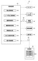
- FIG. 3 is a functional block diagram of the control device 22 of the first embodiment. As shown in FIG. 3, the control device 22 is connected to the operation unit 38 and the storage unit 39 in addition to the monitor 20, the moving mechanism 24, the laser optical system 25, and the observation optical system 30 described above.
- the operation unit 38 uses a known keyboard, mouse, operation buttons, and the like, and accepts input of various operations by the operator.
- the storage unit 39 stores the control program of the laser processing device 10 and the determination result of the processing state of the processing groove 9 by the control device 22. Further, although the details will be described later, the storage unit 39 stores in advance the corresponding information 62 used for determining the processing state of the processing groove 9 by the control device 22.
- the control device 22 is composed of an arithmetic unit such as a personal computer, and includes an arithmetic circuit composed of various processors (Processor), a memory, and the like.
- processors include CPU (Central Processing Unit), FPGA (Graphics Processing Unit), ASIC (Application Specific Integrated Circuit), and programmable logic devices [for example, SPLD (Simple Programmable Logic Devices), CPLD (Complex Programmable Logic Device), And FPGA (Field Programmable Gate Arrays)] and the like.
- the various functions of the control device 22 may be realized by one processor, or may be realized by a plurality of processors of the same type or different types.
- the control device 22 executes a detection control unit 40, a laser processing control unit 42, an imaging control unit 44, an observation image acquisition unit 46, a brightness detection unit 48, and processing. It functions as a state determination unit 50 and a display control unit 52.
- a detection control unit 40 a laser processing control unit 42
- an imaging control unit 44 an imaging control unit 44
- an observation image acquisition unit 46 a brightness detection unit 48
- processing It functions as a state determination unit 50 and a display control unit 52.
- a state determination unit 50 a display control unit 52.
- the detection control unit 40 controls each part of the laser processing apparatus 10 to execute alignment detection for detecting the position (including the orientation in the XY plane) of each street CH of the wafer W held on the suction stage 16. do.
- the detection control unit 40 controls the moving mechanism 24 and the observation optical system 30 to acquire (photograph) the observation image 36 of the alignment reference of the wafer W.
- the alignment standard referred to here is a standard for the laser processing apparatus 10 to recognize the position of the street CH of the wafer W, and for example, a known standard such as a street CH and an alignment mark (not shown) is used. ..
- the alignment reference may be provided at an arbitrary position such as inside, the front surface, and the back surface of the wafer W as long as it can be photographed by the microscope 35.
- the detection control unit 40 drives the moving mechanism 24 to observe the optical axis of the condenser lens 29 relative to the position where the alignment reference of the wafer W can be photographed by the observation optical system 30. Move it. After this movement, the detection control unit 40 causes the microscope 35 to take an image of the wafer W including the alignment reference. As a result, the observation image 36 of the alignment reference of the wafer W is acquired by the microscope 35, and the observation image 36 is output from the microscope 35 to the detection control unit 40.
- the detection control unit 40 detects the position of each street CH of the wafer W by detecting the alignment standard in the observation image by a known image recognition method based on the observation image 36 of the alignment reference input from the microscope 35. do.
- the laser machining control unit 42 controls the moving mechanism 24 and the laser optical system 25 to perform laser machining for each street CH to form a machining groove 9 along the street CH.
- the laser machining control unit 42 drives the moving mechanism 24 to rotate the XYZ ⁇ stage 14 in the ⁇ direction based on the alignment detection result by the detection control unit 40, thereby rotating the street CH to be machined in the X direction (machining). Make it parallel to the feed direction).
- the laser machining control unit 42 drives the moving mechanism 24 to adjust the position of the XYZ ⁇ stage 14 based on the alignment detection result by the detection control unit 40, thereby adjusting the optical axis of the condenser lens 29 to the street to be machined. Perform alignment to align to one end of the CH.
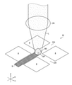
- FIGS. 4 and 5 are explanatory views for explaining the formation of the machined groove 9 along the street CH.
- the laser processing control unit 42 controls the laser optical system 25 to condense the laser beam L onto the street CH to be processed on the wafer W. Then, a machining groove 9 is formed at the machining point SP of the laser beam L.
- the laser machining control unit 42 drives the moving mechanism 24 to move the XYZ ⁇ stage 14 in the X direction.
- the laser optical system 25 is relatively moved in the X direction with respect to the wafer W in a state where the laser beam L is focused on the street CH, that is, the laser optical system 25 is moved along the first street CH. Is moved relative to the wafer W in the X direction.
- the machined groove 9 is formed along the street CH to be machined.
- the surface layer (Low-k film or the like) of the street CH is formed into a so-called plasma in which the surface layer (Low-k film or the like) of the street CH is ionized through melting and vaporization due to the heat of the laser beam L, so that the plasma 60 is formed. Occurs.
- the brightness of the plasma 60 depends on the amount of removed material (depth of the machined groove 9) such as the Low-k film removed (plasmaized) from the street CH per shot of the laser beam L, which is a pulse laser. Will change.
- the amount of removed material removed per shot correlates with the energy (J) of the laser beam L. Therefore, there is a correlation between the brightness of the plasma 60 at each processing point SP, the amount of removed matter removed (depth of the processing groove 9), and the energy of the laser beam L.
- the spot diameter of the laser beam L (machining point SP), the depth position of the machining point SP from the surface of the wafer W (position in the Z direction), and the material of the street CH also have an effect.
- these are described as being constant.
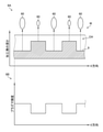
- FIG. 6 is an explanatory diagram for explaining the relationship between the brightness of the plasma 60 (plasma brightness) and the depth of the machined groove 9.
- reference numeral 6A in FIG. 6 as the amount of the removed material removed from the processing point SP on the street CH increases, the brightness of the plasma 60 generated at the processing point SP increases. On the contrary, as the amount of the removed material removed from the processing point SP on the street CH decreases, the brightness of the plasma 60 generated at the processing point SP decreases. Further, when the energy of the laser beam L is increased or decreased, the brightness of the plasma 60 and the amount of removed matter removed at each processing point SP change. Therefore, the brightness of the plasma 60 and the energy of the laser beam L at each processing point SP are indicators of the amount of removed matter removed at each processing point SP, that is, the depth of the processing groove 9.
- correspondence information 62 (see FIG. 3), which will be described later, showing the correspondence between the brightness of the plasma 60, the energy of the laser beam L, and the amount of removed matter removed (depth of the machined groove 9) is provided in advance. I'll ask for it.
- correspondence information is based on the brightness of the plasma 60 for each processing point SP along the street CH (X direction) and the energy of the known laser beam L.
- the depth of the machining groove 9 for each machining point SP is obtained.
- the overall bottom surface shape of the machined groove 9 formed along the street CH can also be obtained.
- the brightness of the plasma 60 also correlates with the temperature of the processing point SP. Therefore, by obtaining the correspondence relationship between the brightness of the plasma 60, the energy of the laser beam L, and the temperature of the processing point SP as the above-mentioned correspondence information 62, each processing point SP along the street CH is obtained. Based on the brightness of the plasma 60 and the energy of the known laser beam L, the depth and the processing temperature of the processing groove 9 for each processing point SP can be obtained.
- the imaging control unit 44 controls the observation optical system 30 while the street CH is laser-processed (formation of the processing groove 9) by the laser optical system 25, and the laser beam is emitted by the microscope 35.
- the imaging of the processing point SP of L and the output of the observation image 36 are repeatedly executed. Since the laser beam L of the present embodiment is a pulse laser, it is preferable that the imaging control unit 44 executes imaging of the processing point SP and output of the observation image 36 in synchronization with the emission trigger of the laser beam L. As a result, a real-time observation image 36 of the processing point SP can be obtained for each processing point SP along the street CH.
- the observation image acquisition unit 46 functions as an interface for connecting to the microscope 35 while the street CH is laser-processed (formation of the processing groove 9) by the laser optical system 25.
- the observation image acquisition unit 46 repeatedly acquires the observation image 36 of the processing point SP from the microscope 35 and outputs it to the luminance detection unit 48 each time the imaging point SP is photographed by the microscope 35.
- the brightness detection unit 48 detects the brightness of the plasma 60 generated at the processing point SP based on the observation image 36 each time the observation image 36 of the processing point SP is input from the observation image acquisition unit 46.
- the brightness detection unit 48 determines the image region of the plasma 60 included in the observation image 36 based on the brightness value for each pixel of the observation image 36. Since the brightness value of the image region of the plasma 60 is higher than the brightness value of the other regions in the observation image 36, the brightness detection unit 48 plasmas, for example, a region in the observation image 36 where the brightness value is equal to or higher than a predetermined threshold value. It is determined as an image area of 60.
- the luminance detection unit 48 detects, for example, the integrated value of the luminance values of the pixels in the image region of the plasma 60 as the “luminance of the plasma 60”. As described above, since the image pickup element of the microscope 35 has sensitivity to the entire wavelength range of the plasma 60, the luminance detection unit 48 converts the light in the entire wavelength range of the plasma 60 into luminance, and the luminance detection unit 48 of the plasma 60 is based on the result. The brightness can be detected.
- the brightness detection unit 48 detects the brightness of the plasma 60 at each processing point SP. Then, each time the brightness detection unit 48 detects the brightness of the plasma 60 at each processing point SP, the brightness detection unit 48 outputs the detection result to the processing state determination unit 50.
- the luminance detection unit 48 determines the maximum value or the average value of the luminance values as the "luminance of the plasma 60". It may be detected as.
- the machining state determination unit 50 is based on the luminance detection result of the plasma 60 for each machining point SP input from the luminance detection unit 48 and the energy of the known laser beam L, and the machining state of the machining groove 9 for each machining point SP. (Depth and temperature of the machined groove 9) is determined.
- the processing state determination unit 50 acquires the correspondence information 62 from the storage unit 39.
- the machining state determination unit 50 functions as the corresponding information acquisition unit of the present invention.
- the machining state determination unit 50 may acquire the correspondence information 62 from the outside of the laser machining apparatus 10 via the Internet or the like, instead of acquiring the correspondence information 62 from the storage unit 39 of the laser machining apparatus 10.
- the correspondence information 62 is information indicating the correspondence relationship between the brightness of the plasma 60, the energy of the laser beam L, and the depth and temperature of the machining groove 9 of the machining point SP, and is generated in advance based on an experiment or a simulation or the like. It is stored in the storage unit 39.
- the correspondence information 62 includes a removal amount calculation formula 62A, a groove depth calculation formula 62B, and a temperature calculation formula 62C.
- the correspondence information 62 of the present embodiment is composed of an arithmetic expression (mathematical expression), a data table or the like showing the above-mentioned correspondence may be used.
- the removal amount calculation formula 62A is a calculation formula showing the correspondence between the brightness of the plasma 60, the energy of the laser beam L, and the removal amount of the removed material at the processing point SP.
- ⁇ , ⁇ , and ⁇ are coefficients related to A, B, and C, respectively, and a, b, and c are intercepts, respectively.
- the processing point is obtained by inputting "B” and “C” into the above-mentioned removal amount calculation formula 62A.
- the removal amount "A” of the removed substance in the SP is obtained.
- the groove depth calculation formula 62B is a calculation formula showing the correspondence between the removal amount “A” of the removed material at the machining point SP and the depth of the machining groove 9.
- a formula capable of deriving the depth of the machined groove 9 is used with the removal amount “A” and the area (spot diameter) of the machined point SP as variables.
- the depth of the machining groove 9 is directly determined from the energy “B”, the brightness “C” of the plasma 60, the area of the machining point SP, and the like. You may use an expression that can be calculated.
- the temperature calculation formula 62C is a calculation formula showing the correspondence between the brightness of the plasma 60, the energy of the laser beam L, and the temperature of the processing point SP.
- the temperature calculation formula 62C similarly to the removal amount calculation formula 62A described above, an formula capable of deriving the temperature of the processing point SP is used with the energy “B” and the luminance “C” of the plasma 60 as variables.
- the processing state determination unit 50 removes at the processing point SP using the removal amount calculation formula 62A based on the brightness “C” of the plasma 60 input from the brightness detection unit 48 and the energy “B” of the known laser beam L. Calculate the removal amount "A” of the object.
- the machining state determination unit 50 uses the groove depth calculation formula 62B at the machining point SP based on the calculation result of the removal amount “A” of the removed material at the machining point SP and the area of the known machining point SP. Calculate the depth of the machined groove 9.
- the machining state determination unit 50 uses the temperature calculation formula 62C to determine the machining point SP based on the luminance “C” of the plasma 60 input from the luminance detection unit 48 and the energy “B” of the known laser beam L. Calculate the temperature.
- the machining state determination unit 50 repeats the calculation of the depth and temperature of the machining groove 9 at the machining point SP every time the luminance “C” of the plasma 60 of the new machining point SP is input from the brightness detection unit 48. Run. As a result, the depth and temperature of the machining groove 9 for each machining point SP along the street CH can be obtained. Further, the stability of the bottom surface shape of the machined groove 9 along the street CH can be evaluated based on the calculation result of the depth of the machined groove 9 for each machined point SP.
- the brightness of the plasma 60 at the processing point SP since there is a relationship between the brightness of the plasma 60 at the processing point SP and the depth and temperature of the processing groove 9 at the processing point SP, the brightness of the plasma 60 for each processing point SP along the street CH It is also possible to evaluate the depth and temperature stability of the machining groove 9 at each machining point SP from the dispersion value.
- the display control unit 52 controls the display of the monitor 20.
- the display control unit 52 causes the monitor 20 to display the observation image 36 output from the microscope 35 and the processing state determination result of the processing groove 9 for each processing point SP by the processing state determination unit 50.
- FIG. 7 is a flowchart showing a flow of laser processing for each street CH of the wafer W by the laser processing apparatus 10 of the first embodiment according to the control method of the present invention.
- the detection control unit 40 of the control device 22 operates.
- the detection control unit 40 controls the moving mechanism 24 and the observation optical system 30 to acquire the observation image 36 of the alignment reference of the wafer W. Then, the detection control unit 40 analyzes the observation image 36 and performs alignment detection to detect the position of each street CH of the wafer W (step S1).
- the laser machining control unit 42 When the alignment detection is completed, the laser machining control unit 42 operates. Then, the laser machining control unit 42 drives the moving mechanism 24 based on the alignment detection result by the detection control unit 40 to align the optical axis of the condenser lens 29 with one end of the first street CH. Execute (step S2).
- the laser machining control unit 42 forms the machining groove 9 by irradiating (condensing) the laser beam L from the laser optical system 25 onto one end of the first street CH (step S3).
- the surface layer (Low-k film or the like) of the street CH is turned into plasma by the heat of the laser beam L, so that the plasma 60 is generated.
- the laser machining control unit 42 drives the moving mechanism 24 to move the XYZ ⁇ stage 14 in the X direction, thereby moving the laser optical system 25 relative to the wafer W in the X direction (step S4).
- laser machining that is, formation of the machined groove 9, is started along the first street CH.
- the imaging control unit 44 and the observation image acquisition unit 46 operate in accordance with the start of laser processing.
- the imaging control unit 44 controls the microscope 35 of the observation optical system 30 in synchronization with, for example, the emission trigger of the laser beam L to perform imaging of the processing point SP of the laser beam L, and the observation image acquisition unit 46 performs imaging.
- the acquisition of the observation image 36 of the processing point SP from the microscope 35 and the output to the brightness detection unit 48 are executed (step S5, corresponding to the observation image acquisition step of the present invention).
- the luminance detection unit 48 Upon receiving the input of the observation image 36 of the processing point SP, the luminance detection unit 48 discriminates the image region of the plasma 60 from the observation image 36, and for example, the luminance of the plasma 60 is based on the luminance value of the pixels in this image region. (Step S6, corresponding to the brightness detection step of the present invention). Then, the luminance detection unit 48 outputs the luminance detection result of the plasma 60 to the machining state determination unit 50.
- the processing state determination unit 50 that has received the input of the luminance detection result of the plasma 60 first acquires the correspondence information 62 from the storage unit 39 (step S7, corresponding to the correspondence information acquisition step of the present invention). Then, the machining state determination unit 50 uses the correspondence information 62 based on the luminance detection result of the plasma 60 and the known energy of the laser beam L, and the machining state of the machining groove 9 at the machining point SP (depth of the machining groove 9). (The temperature) is determined (step S8, corresponding to the processing state determination step of the present invention).
- the machining state determination unit 50 causes the monitor 20 to display the determination result of the machining state via the display control unit 52.
- the observation image 36 is acquired and the brightness of the plasma 60 is detected for each processing point SP along the street CH.
- the determination of the processing state of the processing groove 9 using the information 62 and the display of the determination result of the processing state are repeatedly executed (NO in step S9).
- the operator can evaluate the depth of the machining groove 9 at each machining point SP in real time without breaking the wafer W, and further, this machining groove is based on the depth of the machining groove 9 at each machining point SP.
- the bottom surface shape of 9 can be evaluated in real time. Further, the operator can evaluate the damage due to the temperature in real time based on the temperature determination result for each machining point SP.
- the laser processing control unit 42 performs the relative movement of the laser optical system 25 by the moving mechanism 24 and the irradiation of the laser beam L from the laser optical system 25.
- the imaging control unit 44 stops imaging by the observation optical system 30 (step S10).
- step S11 laser processing of the second street CH is started (NO in step S11). Similarly, the processes from step S2 to step S10 are repeatedly executed for each of the second and subsequent street channels (YES in step S11). As a result, acquisition of the observation image 36, brightness detection of the plasma 60, determination of the processing state of the processing groove 9, and display of the processing state determination result are repeated for each processing point SP along each street CH. Will be executed.
- each processing point SP based on the detection result of the brightness of the plasma 60 for each processing point SP that moves along the street CH during laser processing for each street CH, each processing point SP The processing state (depth and temperature of the processing groove 9) of laser processing can be discriminated (monitored) in real time. As a result, the depth of the machined groove 9 at each machined point SP, the stability of the bottom surface shape of the machined groove 9, and the damage due to temperature can be evaluated in real time.
- FIG. 8 is a schematic view of the laser processing apparatus 10 of the second embodiment.
- the brightness of the plasma 60 is detected from the observation image 36 of the processing point SP taken by the microscope 35.
- the wavelength range of the plasma 60 is broad, the wavelength range of the laser beam L is included in the wavelength range of the plasma 60, and the brightness detection result of the plasma 60 by the brightness detection unit 48 of the first embodiment shows. Also includes the influence of the scattered light of the laser beam L at the processing point SP. Therefore, the laser processing apparatus 10 of the second embodiment suppresses the influence of the scattered light of the laser beam L included in the detection result of the brightness of the plasma 60.
- the laser processing device 10 of the second embodiment has basically the same configuration as the laser processing device 10 of the first embodiment except that the filter 65 is provided. Therefore, those having the same function or configuration as those of the first embodiment are designated by the same reference numerals and the description thereof will be omitted.
- the filter 65 corresponds to the optical element of the present invention, and is provided on the optical path between the condenser lens 34 and the microscope 35.
- the arrangement position of the filter 65 is not particularly limited as long as it is a position on the optical path from the wafer W to the microscope 35 and excluding the optical path of the laser beam L from the laser light source 26 to the wafer W. Further, the filter 65 may be provided in the microscope 35.
- the filter 65 blocks the light in the wavelength range of the laser beam L, that is, prevents the light in the wavelength range of the laser beam L from incident on the microscope 35.
- various known filters such as a high-pass filter, a low-pass filter, and a band-pass filter that transmit or block light in a specific wavelength range are used.
- a dichroic mirror, a dichroic prism, or the like may be used instead of the filter 65.
- the microscope 35 of the second embodiment takes an image of the processing point SP through the filter 65 while the laser processing of each street CH is being performed. This prevents the image pickup element of the microscope 35 from capturing light in the wavelength range of the laser beam L.
- the brightness detection unit 48 of the second embodiment can detect the brightness of the plasma 60 based on the light in the wavelength range excluding the wavelength range of the laser beam L in the entire wavelength range of the plasma 60.
- the filter 65 by blocking the light in the wavelength range of the laser light L incident on the microscope 35 by the filter 65, the influence of the scattered light of the laser light L included in the detection result of the brightness of the plasma 60 (Noise) can be suppressed. As a result, it is possible to determine the machining state of the machining groove 9 for each machining point SP with higher accuracy.
- an actuator (not shown) may be used to freely insert and remove the filter 65 in the optical path between the condenser lens 34 and the microscope 35. good.
- the filter 65 can be retracted from the above-mentioned optical path in cases other than laser processing of each street CH such as alignment detection.
- the laser processing apparatus 10 according to the third embodiment of the present invention will be described.
- the processing conditions other than the energy of the laser beam L have been described as being the same, but the laser processing apparatus 10 of the third embodiment has a plurality of laser processing devices 10. Laser processing of each street CH is selectively performed according to the processing conditions.
- FIG. 9 is an explanatory diagram showing an example of processing conditions for laser processing of each street CH.
- the laser machining apparatus 10 of the third embodiment for example, the depth position (Z direction position) of the machining point SP from the surface of the wafer W and the removed material generated by the formation of the machining groove 9 are formed.
- Laser machining of each street CH is selectively performed under three first machining conditions to third machining conditions in which at least one of the removal amounts of the above is different.
- the depth position of the machining point SP is set near the surface of the wafer W, and the amount of removed material removed is large (that is, the depth of the machining groove 9). Is set to be deeper). Under this first processing condition, the brightness of the plasma 60 is increased as compared with the other processing conditions.
- the depth position of the machining point SP is set to a position deeper than the first machining condition (inside the wafer W), and the amount of removed material removed is large. It is set to be.
- the plasma 60 enters the inside of the wafer W more than the first processing condition, so that the brightness of the plasma 60 observed by the observation optical system 30 is lower than that of the first processing condition.
- the depth position of the machining point SP is set near the surface of the wafer W, and the amount of removed material removed is small (that is, the depth of the machining groove 9). Is set to be shallow). Under this third processing condition, the brightness of the plasma 60 is reduced as compared with the other processing conditions.
- the number of processing conditions may be increased to 4 or more by including the spot diameter of the laser beam L (processing point SP) and the material of the street CH (wafer W) in the processing conditions.
- the brightness of the plasma 60 observed by the observation optical system 30 changes even when the processing conditions other than the energy of the laser beam L are different. Therefore, even if the energy of the laser beam L and the brightness of the plasma 60 under each processing condition are the same, the depth of the processing groove 9 formed at the processing point SP and the processing point SP for each processing condition. The temperatures are different from each other. Therefore, in the laser machining apparatus 10 of the third embodiment, the machining state of the machining groove 9 for each machining point SP is determined by using the corresponding information 62 that differs depending on the machining conditions.
- FIG. 10 is a functional block diagram of the control device 22 of the laser processing device 10 of the third embodiment.
- a plurality of correspondence information 62 corresponding to a plurality of processing conditions are stored in the storage unit 39.
- the structure is basically the same as that of the laser processing apparatus 10 of each of the above-described embodiments. Therefore, those having the same function or configuration as each of the above-described embodiments are designated by the same reference numerals and the description thereof will be omitted. ..
- Each correspondence information 62 is information indicating the correspondence relationship between the "luminance of the plasma 60", the "energy of the laser beam L", and the "depth and temperature of the machining groove 9 of the machining point SP" for each machining condition, and is information in advance. It is generated for each processing condition based on an experiment, simulation, or the like and stored in the storage unit 39.
- the operation unit 38 of the third embodiment accepts a selection operation for selecting processing conditions.
- the operation unit 38 functions as the processing condition selection unit of the present invention.
- the laser machining control unit 42 of the third embodiment controls the moving mechanism 24 and the laser optical system 25 according to the machining conditions (depth position of the machining point SP, etc.) selected by the operation section 38, and the street to be machined.
- a machined groove 9 is formed along the CH.
- the machining state determination unit 50 of the third embodiment acquires the correspondence information 62 corresponding to the machining conditions selected by the operation unit 38 from the storage unit 39.
- the machining state determination unit 50 receives the luminance detection result and the known laser beam each time the luminance detection result of the plasma 60 at the new machining point SP is input from the luminance detection unit 48. Based on the energy of L, the machining state of the machining groove 9 at the machining point SP is determined by using the correspondence information 62 previously acquired.
- the machining state of the machined groove 9 can be discriminated by using the corresponding information 62 different for each machining condition, the machining state of the machined groove 9 can be discriminated more accurately. ..
- FIG. 11 is an enlarged view of a street CH subjected to laser processing by the laser processing apparatus 10 of the fourth embodiment.
- the surface of the street CH is made of the same material (for example, silicon dioxide) by a Low-K film or the like, but as shown in FIG. 11, a part of the surface of the street CH is TEG.
- the pattern 66 such as Test Element Group
- the pattern 66 may be formed of a metal such as aluminum.
- on the surface of the street CH there are a plurality of regions having different materials, including a region where a Low-K film or the like (silicon dioxide or the like) is exposed and a region where a pattern 66 (aluminum or the like) is formed. Exists.
- the relationship between the energy of the laser beam L, the brightness of the plasma 60, and the processing state of the processing groove 9 at the processing point SP is different for each of these materials.
- the laser machining apparatus 10 of the fourth embodiment determines the machining state of the machining groove 9 for each machining point SP by using the corresponding information 62 that differs depending on the material of the surface of the street CH.
- FIG. 12 is a functional block diagram of the control device 22 of the laser processing device 10 of the fourth embodiment.
- the position detection sensor 70 is connected to the control device 22, and the control device 22 functions as a position information acquisition unit 72 in addition to the above-mentioned parts.
- the configuration is basically the same as that of the laser processing apparatus 10 of each of the above embodiments, except that the design information 74 and the plurality of correspondence information 63 are stored in the storage unit 39. Therefore, those having the same function or configuration as each of the above embodiments are designated by the same reference numerals, and the description thereof will be omitted.
- the position detection sensor 70 is provided in, for example, the XYZ ⁇ stage 14, detects the position of the XYZ ⁇ stage 14 in the XYZ ⁇ direction, and outputs the position detection result to the position information acquisition unit 72.
- the position information acquisition unit 72 is the processing point SP on the street CH based on the position detection result of the XYZ ⁇ stage 14 input from the position detection sensor 70 while the laser processing of the street CH is being performed by the laser optical system 25.
- the X-direction position indicating the relative position of is repeatedly detected, and the X-direction position of the machining point SP is repeatedly output to the machining state determination unit 50.
- the detection of the X-direction position of the processing point SP by the position information acquisition unit 72 is executed in synchronization with the emission trigger of the laser beam L, that is, in synchronization with the shooting of the processing point SP described above. Is preferable.
- the design information 74 is information indicating the material of each street CH of the wafer W for each position in the X direction (for each region).
- Each correspondence information 63 is information showing the correspondence relationship between "brightness of plasma 60", "energy of laser beam L” and “depth and temperature of machining groove 9 of machining point SP" for each material of street CH. , Is generated in advance for each processing condition based on an experiment, simulation, or the like, and is stored in the storage unit 39.
- the processing state determination unit 50 of the fourth embodiment is based on the detection result of the X-direction position of the processing point SP input from the position information acquisition unit 72 while the laser processing of the street CH is performed by the laser optical system 25. , The material of the surface of the street CH at the position of the machining point SP is determined with reference to the design information 74, and the corresponding information 63 corresponding to this material is acquired from the storage unit 39. Then, the processing state determination unit 50 uses the corresponding information 63 previously acquired based on the brightness detection result of the plasma 60 input from the brightness detection unit 48 and the energy of the known laser beam L, and uses the corresponding information 63 of the processing point SP. The processing state of the processing groove 9 is determined.
- the machining state determination unit 50 detects the position of the machining point SP in the X direction for each machining point SP, discriminates the material of the surface of the street CH, acquires the corresponding information 63, and performs the machining groove 9 of the machining point SP. And repeatedly execute the determination of the processing state of.
- FIG. 13 is a flowchart showing the flow of laser processing for each street CH of the wafer W by the laser processing apparatus 10 of the fourth embodiment. Since the processes from step S1 to step S6 are the same as those in the first embodiment (see FIG. 7), a specific description thereof will be omitted here.
- the position information acquisition unit 72 parallels with steps S5 and S6 described above, based on the position detection result of the position detection sensor 70.
- the X-direction position of the machining point SP is detected in synchronization with the emission trigger of the laser beam L, and the X-direction position of the machining point SP is output to the machining state determination unit 50 (step S6A).
- the machining state determination unit 50 refers to the design information 74 based on the detection result of the X-direction position of the machining point SP input from the position information acquisition unit 72, and the machining state SP is the surface of the street CH at the position of the machining point SP.
- the material is determined (step S6B), and the corresponding information 63 corresponding to the material of the processing point SP is acquired from the storage unit 39 (step S7A).
- the machining state determination unit 50 discriminates the machining state of the machining groove 9 of the machining point SP by using the correspondence information 63 based on the luminance detection result of the plasma 60 in step S6 and the energy of the known laser beam L. (Step S8).
- step S5 to step S8 are repeatedly executed for each machining point SP along the street CH.
- the machining state of the machining groove 9 is discriminated by the machining state discriminating unit 50 based on the corresponding information 63 corresponding to the material of each machining point SP. Since the subsequent processing is basically the same as that of the first embodiment, specific description thereof will be omitted here.
- the material of the machining point SP is discriminated for each position of the machining point SP, and the machining state of the machining groove 9 is discriminated by using the corresponding information 63 corresponding to the material of the machining point SP.
- the laser processing apparatus 10 determines the machining state of the machining groove 9 for each machining point SP, but the laser machining apparatus 10 of the fifth embodiment has the machining state of the machining groove 9 for each machining point SP. Based on the discrimination result, feedback control of laser machining is performed so that the machining state is maintained constant.
- the laser processing device 10 of the fifth embodiment has basically the same configuration as the laser processing device 10 of each of the above embodiments, the same reference numerals are given to those having the same function or configuration as each of the above embodiments. The explanation will be omitted.
- FIG. 14 is a flowchart showing the flow of laser processing for each street CH of the wafer W by the laser processing apparatus 10 of the fifth embodiment. Since the processes from step S1 to step S6 are the same as those of the above embodiments (see FIGS. 7 and 13), specific description thereof will be omitted here.
- the laser machining control unit 42 determines the machining state of the machining groove 9, for example, the depth of the machining groove 9.
- Feedback control is performed to control the energy of the laser beam L emitted from the laser optical system 25 so that the value is kept constant (step S8A).
- the energy control of the laser beam L is to increase or decrease the energy (J) of the laser beam L by increasing or decreasing at least one of the output (watt) and the time (sec) of the laser beam L.
- the laser machining control unit 42 increases the energy (J) of the laser beam L emitted from the laser optical system 25 when the depth of the machining groove 9 is less than a predetermined design value.
- the laser machining control unit 42 reduces the energy (J) of the laser beam L emitted from the laser optical system 25 when the depth of the machining groove 9 becomes larger than the design value.
- the laser machining control unit 42 will perform the above-mentioned feedback control every time the machining state determination unit 50 determines the depth of the machining groove 9 at the machining point SP until the laser machining of the street CH to be machined is completed. Is repeatedly executed (step S9). Since the subsequent processing is basically the same as that of each of the above embodiments, a specific description thereof will be omitted here.
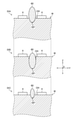
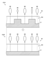
- FIG. 15 is an explanatory diagram for explaining the effect of the laser processing apparatus 10 of the fifth embodiment.
- the reference numeral XVA in FIG. 15 is an example of the machining groove 9 for each machining point SP when the above-mentioned feedback control is not performed, and the reference numeral XVB is an example of the machining groove 9 for each machining point SP when the above-mentioned feedback control is performed. Is an example of.
- the depth of the machining groove 9 for each machining point SP is determined in real time based on the detection result of the brightness of the plasma 60 for each machining point SP.
- the energy of the laser beam L can be controlled to keep the depth of the machined groove 9 constant.
- the depth of the machined groove 9 along the street CH can be kept constant. Thereby, the processing quality of the processing groove 9 can be improved.
- FIG. 16 is a block diagram showing the configuration of the wafer processing system 100 according to the sixth embodiment of the present invention.
- the case where the laser machining apparatus 10 is used alone has been described as an example, but in the sixth embodiment, a plurality of (or even one) laser machining apparatus 10 are connected to the server 200.
- the server 200 generates the correspondence information 62 (including the correspondence information 63) and distributes the correspondence information 62 to each laser processing apparatus 10.
- the wafer processing system 100 includes a plurality of laser processing devices 10 and a server 200. Those having the same function or configuration as each of the above embodiments are designated by the same reference numerals, and the description thereof will be omitted.
- At least one laser processing device 10 among the plurality of laser processing devices 10 has a function of generating actual measurement information 84 used for generating the corresponding information 62.
- the actual measurement information 84 includes the position in the X direction for each processing point SP along the street CH, the detected value of the plasma luminance, the energy of the laser beam L, the shape of the processing groove 9 (actual measurement value), and the like.
- the laser processing device 10 is provided with a white interferometer 55 in addition to the above-mentioned parts, and the control device 22 functions as a position information acquisition unit 72, a groove shape acquisition unit 80, and an actual measurement information output unit 82. It has basically the same configuration as the laser processing apparatus 10 of each of the above embodiments.
- the white interferometer 55 As the white interferometer 55, a known type such as the Michaelson type is used. In the white interferometer 55, every time a processing groove 9 is formed at each processing point SP along the street CH while the laser processing of the street CH to be processed is being performed, the processing groove 9 is formed through, for example, a condenser lens 29. (For example, see JP-A-2018-146391). Based on this interference image, the groove shape of the machined groove 9 formed at the machined point SP [height information (depth information) of each part of the bottom surface of the machined groove 9] can be obtained.
- the groove shape acquisition unit 80 is the groove shape of the machined groove 9 based on the interference image acquired from the white interferometer 55 for each machined point SP along the street CH while the laser machine of the street CH to be machined is being machined. Is calculated and the calculation result is output to the actual measurement information output unit 58. Similarly, the groove shape acquisition unit 80 calculates the groove shape of the machined groove 9 at each machined point SP along the street CH every time the laser machining of all the street CHs is executed, and actually measures the calculation result. Output to the information output unit 58.
- the actual measurement information output unit 82 receives the X-direction position of the processing point SP from the position information acquisition unit 72 and the luminance detection unit 48 for each processing point SP while the laser processing of the street CH to be processed is being performed.
- the luminance detection result of the plasma 60, the energy information of the laser beam L from the laser optical system 25, and the groove shape calculation result of the machined groove 9 from the groove shape acquisition unit 80 are acquired.
- the actual measurement information output unit 82 generates the actual measurement information 84 based on these acquisition results.
- the relationship between the position in the X direction for each processing point SP along the street CH, the plasma brightness, the energy of the laser beam L, and the groove shape (measured value) of the processing groove 9 can be obtained.
- the actual measurement information output unit 82 generates the actual measurement information 84 every time the laser processing of all the street channels is executed. Then, the actual measurement information output unit 82 outputs the actual measurement information 84 for each street CH of the wafer W to the server 200.
- the server 200 is composed of an arithmetic circuit composed of various processors, memories, and the like, and functions as a corresponding information generation unit 202 and a storage unit 204.
- the correspondence information generation unit 202 generates the correspondence information 62 corresponding to the type of the wafer W based on the actual measurement information 84 for each street CH of the wafer W input from the actual measurement information output unit 82.
- the correspondence information generation unit 202 stores the generated correspondence information 62 in the storage unit 204 in a state associated with the type of the wafer W.
- Correspondence information 62 generated by the correspondence information generation unit 202 is stored in the storage unit 204 for each type of wafer W.
- the machining state determination unit 50 of each laser machining apparatus 10 can discriminate the machining state of the machining groove 9 for each machining point SP by using the corresponding information 62 stored in the storage section 204 of the server 200. can.
- the design information 74 described above may be stored in the storage unit 204 for each type of wafer W.
- the correspondence information 62 can be generated by providing the laser machining apparatus 10 with a function for acquiring the shape of the machining groove 9 (white interferometer 55). As a result, it is possible to easily cope with laser machining (monitoring of machining state) of a new wafer W. Further, in the sixth embodiment, by storing the correspondence information 62 in the storage unit 204 of the server 200, the correspondence information 62 can be shared by the plurality of laser processing devices 10.
- the groove shape of the machined groove 9 is acquired by using the white interferometer 55, but various shape measuring devices such as various interferometers, distance measuring devices, laser scanners, and stereo cameras are used.
- the groove shape of the machined groove 9 may be acquired.
- the laser processing apparatus 10 may be provided with a temperature sensor (radiation thermometer or the like) for measuring the temperature of the processing point SP, and the temperature may be measured at each processing point SP.
- a temperature sensor radiation thermometer or the like
- the server 200 is provided with the corresponding information generation unit 202, but the control device 22 of the laser processing device 10 may be provided with the corresponding information generation unit 202.
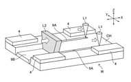
- FIG. 17 is an explanatory diagram for explaining the formation of the two edge cutting grooves 9A and the hollow groove 9B along the street CH by the laser processing device 10.
- the laser machining apparatus 10 of each of the above embodiments forms one machining groove 9 along the street CH, but the present invention is not limited thereto.
- the present invention can also be applied to a laser machining apparatus 10 that performs a hollowing process for forming a hollowing groove 9B (divided groove) between the edge cutting grooves 9A (see Patent Document 1 above).
- the machining states of the two edge cutting grooves 9A and the hollow groove 9B can be determined in real time for each machining point SP of the laser beams L1 and L2.
- the XYZ ⁇ stage 14 and the moving mechanism 24 have been described as examples of the moving mechanism of the present invention, but the configuration is not particularly limited as long as the machining unit 18 and the wafer W can be moved relative to each other.
- the irradiation optical axis of the laser optical system 25 and the observation optical axis of the observation optical system 30 are coaxial, but if the processing point SP is included in the observation field of the observation optical system 30, the illumination light
- the axis and the observation optical axis may be different. That is, the laser optical system 25 and the observation optical system 30 may be provided separately.
- control device 22 may be provided separately from the laser processing device 10.
- control device 22 corresponds to the laser processing device of the present invention.
- the depth of the machined groove 9 and the temperature of the machined point SP are determined as the machined state of the machined groove 9 for each machined point SP, but the type of the machined state is not particularly limited. No.
Landscapes
- Engineering & Computer Science (AREA)
- Physics & Mathematics (AREA)
- Optics & Photonics (AREA)
- Plasma & Fusion (AREA)
- Mechanical Engineering (AREA)
- Laser Beam Processing (AREA)
- Dicing (AREA)
- Exposure Of Semiconductors, Excluding Electron Or Ion Beam Exposure (AREA)
Abstract
加工溝の加工状態をリアルタイムで確認可能なレーザ加工装置、ウェーハ加工システム及びレーザ加工装置の制御方法を提供する。レーザ光学系からレーザ光をストリートに照射することでストリートに沿って加工溝を形成するレーザ加工装置において、加工溝の形成中、レーザ光学系からストリートに照射されるレーザ光の加工点の観察像を繰り返し取得する観察像取得部と、観察像取得部が観察像を取得するごとに、観察像に基づき、レーザ光の照射により加工点で発生するプラズマの輝度を検出する輝度検出部と、輝度と、レーザ光のエネルギーと、加工溝の加工状態と、の対応関係を示す対応情報を取得する対応情報取得部と、輝度検出部が輝度を検出するごとに、輝度と既知のレーザ光のエネルギーとに基づき対応情報を参照して加工状態を判別する加工状態判別部と、を備える。
Description
本発明は、ウェーハのレーザ加工を行うレーザ加工装置、ウェーハ加工システム及びレーザ加工装置の制御方法に関する。
近年の半導体デバイスの製造分野では、シリコン等の基板の表面にガラス質材料からなる低誘電率絶縁体被膜(Low-k膜)と回路を形成する機能膜とを積層した積層体により複数のデバイスを形成しているウェーハ(半導体ウェーハ)が知られている。このようなウェーハは、複数のデバイスが格子状のストリートによって格子状に区画されており、ウェーハをストリートに沿って分割することにより個々のデバイスが製造される。
ウェーハを複数のデバイス(チップ)に分割する方法として、高速回転するブレードを用いる方法、ウェーハの内部にストリートに沿ってレーザ加工領域を形成してこのレーザ加工領域が形成されることにより強度が低下したストリートに沿って外力を加える方法が知られている。しかしながら、Low-k膜が適用されたウェーハの場合、Low-k膜の素材とウェーハの素材とが異なるため、前者の方法ではブレードによりLow-k膜と基板とを同時に切削することが困難である。また、後者の方法ではストリート上にLow-k膜が存在する場合に良好な品質で個々のデバイスに分割することが困難である。
そこで、特許文献1及び特許文献2には、ウェーハに対してレーザ光学系をストリートに沿った加工送り方向に相対移動させつつレーザ光学系からレーザ光を前記ストリートに照射することでストリートに沿って加工溝を形成するレーザ加工装置が開示されている。このレーザ加工装置によれば、ストリートに沿って加工溝を形成することでストリート上からLow-k膜等を除去することができる。
ところで、上記特許文献1に記載のレーザ加工装置等を用いてストリートに沿って加工溝を形成するレーザ加工(アブレーション溝加工)を行う場合には、加工溝の加工状態をリアルタイムで確認することが望ましい。この場合には、レーザ加工装置に設けられている顕微鏡(カメラ)を用いてレーザ光の加工点の観察を行うことが考えられるが、顕微鏡を用いた表面観察で得られる加工溝の情報は限られている。このため、従来では、加工溝の加工状態をリアルタイムで確認することができず、レーザ加工後のウェーハを割断してウェーハの加工状態を確認する必要があった。
本発明はこのような事情に鑑みてなされたものであり、加工溝の加工状態をリアルタイムで確認可能なレーザ加工装置、ウェーハ加工システム及びレーザ加工装置の制御方法を提供することを目的とする。
本発明の目的を達成するためのレーザ加工装置は、ウェーハに対してレーザ光学系をウェーハのストリートに沿った加工送り方向に相対移動させつつレーザ光学系からレーザ光をストリートに照射することでストリートに沿って加工溝を形成するレーザ加工装置において、加工溝の形成中、レーザ光学系からストリートに照射されるレーザ光の加工点の観察像を繰り返し取得する観察像取得部と、観察像取得部が観察像を取得するごとに、観察像に基づき、レーザ光の照射により加工点で発生するプラズマの輝度を検出する輝度検出部と、輝度と、レーザ光のエネルギーと、加工溝の加工状態と、の対応関係を示す対応情報を取得する対応情報取得部と、輝度検出部が輝度を検出するごとに、輝度と既知のレーザ光のエネルギーとに基づき対応情報を参照して加工状態を判別する加工状態判別部と、を備える。
このレーザ加工装置によれば、加工点ごとのプラズマの輝度の検出結果に基づき、加工点ごとのレーザ加工の加工状態をリアルタイムに判別することができる。
本発明の他の態様に係るレーザ加工装置において、観察像取得部が、レーザ光の波長域の光を遮断する光学素子と、光学素子を通して加工点を撮影する観察光学系と、を含む。これにより、プラズマの輝度の検出結果に含まれるレーザ光の散乱光の影響(ノイズ)を抑えることができるので、加工点ごとの加工溝の加工状態の判別をより高精度に行うことができる。
本発明の他の態様に係るレーザ加工装置において、対応情報取得部が、輝度と、レーザ光のエネルギーと、加工溝の深さ及び加工点の温度を含む加工状態と、の対応関係を示す対応情報を取得する。これにより、加工点ごとのレーザ加工の加工状態(加工溝の深さ及び加工点の温度)をリアルタイムに判別することができる。
本発明の他の態様に係るレーザ加工装置において、レーザ光学系が、ウェーハの表面からの加工点の深さ位置、及び加工溝の形成により発生する除去物の除去量の少なくともいずれか1つが異なる複数の加工条件で選択的に加工溝の形成が可能であり、加工条件を選択する加工条件選択部を備え、対応情報取得部が、複数の加工条件に対応する複数の対応情報の中から加工条件選択部が選択した加工条件に対応する対応情報を取得する。これにより、加工条件ごとに加工溝の加工状態を判別することができるので、加工溝の加工状態をより正確に判別することができる。
本発明の他の態様に係るレーザ加工装置において、ストリートに沿って互いに材質の異なる複数の領域が存在する場合に、対応情報取得部が、領域ごとの材質に対応した複数の対応情報を取得し、加工点の位置情報を取得する位置情報取得部を備え、加工状態判別部が、位置情報取得部が取得した位置情報と既知のウェーハの設計情報とに基づき、加工点の位置での材質に対応する対応情報を用いて、加工状態の判別を行う。これにより、ストリートの表面に材質が異なる複数の領域が存在している場合であっても加工溝の加工状態の判別を正確に行うことができる。
本発明の他の態様に係るレーザ加工装置において、加工溝の形成が行われている間、加工状態判別部の判別結果に基づき、レーザ光学系が出射するレーザ光のエネルギーを制御して、加工状態を一定に維持するレーザ加工制御部を備える。これにより、加工溝の加工品質を向上させることができる。
本発明の目的を達成するためのウェーハ加工システムは、前述のレーザ加工装置と、対応情報を記憶する記憶部を有するサーバと、を備え、対応情報取得部が、記憶部から対応情報を取得する。
本発明の他の態様に係るウェーハ加工システムにおいて、少なくとも1つのレーザ加工装置が、ストリートに沿った加工点ごとに、加工点に形成された加工溝の少なくとも深さを含む溝形状を取得する溝形状取得部と、輝度検出部の検出結果及び溝形状取得部の取得結果に基づき、加工点ごとの輝度及び溝形状の実測情報をサーバへ出力する実測情報出力部と、を備え、サーバが、実測情報出力部から出力された実測情報に基づき、対応情報を生成して記憶部に記憶させる対応情報生成部を備える。これにより、新規のウェーハWのレーザ加工(加工状態のモニタリング)に容易に対応することができる。
本発明の目的を達成するためのレーザ加工装置の制御方法は、ウェーハに対してレーザ光学系をウェーハのストリートに沿った加工送り方向に相対移動させつつレーザ光学系からレーザ光をストリートに照射することによりストリートに沿って加工溝を形成するレーザ加工装置の制御方法において、加工溝の形成中、レーザ光学系からストリートに照射されるレーザ光の加工点の観察像を繰り返し取得する観察像取得ステップと、観察像取得ステップで観察像を取得するごとに、観察像に基づき、レーザ光の照射により加工点で発生するプラズマの輝度を検出する輝度検出ステップと、輝度と、レーザ光のエネルギーと、加工溝の加工状態と、の対応関係を示す対応情報を取得する対応情報取得ステップと、輝度検出ステップで輝度を検出するごとに、輝度と既知のレーザ光のエネルギーとに基づき対応情報を参照して加工状態を判別する加工状態判別ステップと、を有する。
本発明は、加工溝の加工状態をリアルタイムで確認することができる。
[第1実施形態のレーザ加工装置の構成]
図1は、第1実施形態のレーザ加工装置10の概略図である。図1に示すように、レーザ加工装置10は、ウェーハW(例えばシリコンウェーハ)を複数のチップ4(図2参照)に分割する割断プロセスの前工程として、ウェーハWに対してレーザ加工(アブレーション溝加工)を施す。なお、図中のXYZ方向は互いに直交し、このうちX方向及びY方向は水平方向であり、Z方向は鉛直方向(ウェーハWの厚み方向)である。またθ方向は、Z方向を回転軸とする回転方向である。
図1は、第1実施形態のレーザ加工装置10の概略図である。図1に示すように、レーザ加工装置10は、ウェーハW(例えばシリコンウェーハ)を複数のチップ4(図2参照)に分割する割断プロセスの前工程として、ウェーハWに対してレーザ加工(アブレーション溝加工)を施す。なお、図中のXYZ方向は互いに直交し、このうちX方向及びY方向は水平方向であり、Z方向は鉛直方向(ウェーハWの厚み方向)である。またθ方向は、Z方向を回転軸とする回転方向である。
図2は、レーザ加工装置10による加工対象のウェーハWの平面図である。図2に示すように、ウェーハWは、シリコン等の基板の表面にLow-k膜と回路を形成する機能膜とを積層した積層体である。ウェーハWは格子状に配列された複数のストリートCH(分割予定ラインともいう)によって複数の領域に区画されている。この区画された各領域にはチップ4(デバイス)が設けられている。レーザ加工装置10は、ストリートCHごとにストリートCHに沿ってレーザ加工を行うことで、ストリートCH上のLow-k膜等を除去して加工溝9(アブレーション溝又はレーザグルーブともいう)を形成する。
図1に戻って、レーザ加工装置10は、ベース12と、XYZθステージ14と、吸着ステージ16と、加工ユニット18と、モニタ20と、制御装置22と、を備える。
ベース12上には、XYZθステージ14が設けられている。XYZθステージ14は、ベース12上においてXYZ方向に移動自在で且つθ方向に回転自在に設けられている。このXYZθステージ14は、アクチュエータ及びモータ等により構成される移動機構24(図3参照)によりXYZ方向に移動されると共にθ方向に回転される。
吸着ステージ16は、XYZθステージ14上に設けられている。この吸着ステージ16は、ウェーハWの裏面を吸着保持する。これにより、ウェーハWは、上述のLow-k膜等が形成されている側の表面が後述の加工ユニット18と対向するようにXYZθステージ14に保持される。移動機構24によりXYZθステージ14をXYZθ方向に移動させることで、吸着ステージ16上のウェーハWに対して加工ユニット18がXYZθ方向に相対移動される。
加工ユニット18は、レーザ光学系25及び観察光学系30を備える。この加工ユニット18は、吸着ステージ16のZ方向上方側の位置(ウェーハWに対向する位置)に配置されており、後述の制御装置22により制御される。
レーザ光学系25は、ウェーハWのストリートCHに向けてレーザ光Lを照射する。このレーザ光学系25は、レーザ光源26(レーザ発振器)、コリメートレンズ27、ハーフミラー28、及び集光レンズ29(コンデンスレンズ)を含む。
レーザ光源26は、レーザ光L(例えばパルスレーザ光)をコリメートレンズ27に向けて出射する。レーザ光Lの条件は、例えば、光源:UV(紫外線)-パルスレーザ、波長:400nm以下、繰り返し周波数:1~100kHz、及び平均出力:0.5~10ワットであるが、この条件に特に限定されるものではない。
コリメートレンズ27は、レーザ光源26から入射したレーザ光Lを平行光束に変換した後、このレーザ光Lをハーフミラー28に向けて出射する。
ハーフミラー28は、集光レンズ29の光軸上に配置されており、コリメートレンズ27から入射したレーザ光Lの一部を集光レンズ29に向けて反射する。また、ハーフミラー28は、後述のハーフミラー33から入射した後述の照明光ILの一部を透過して集光レンズ29に向けて出射すると共に、集光レンズ29から入射した照明光ILの反射光の一部を透過してハーフミラー33に向けて出射する。
集光レンズ29は、ハーフミラー28から入射したレーザ光L及び照明光ILをウェーハWのストリートCH上に集光させる。
観察光学系30は、レーザ光学系25と同軸に設けられており、ウェーハWのレーザ加工前にはウェーハWに形成されている後述のアライメント基準を撮影する。また、観察光学系30は、ウェーハWのストリートCHのレーザ加工中にはその加工点SPを撮影する。
観察光学系30は、ハーフミラー28及び集光レンズ29をレーザ光学系25と共用すると共に、照明光源31、コリメートレンズ32、ハーフミラー33、集光レンズ34、及び顕微鏡35等を備える。
照明光源31は、例えば可視光の波長域(赤外光又は近赤外光の波長域でも可)の照明光ILをコリメートレンズ32に向けて出射する。
コリメートレンズ32は、照明光源31から入射した照明光ILを平行光束に変換した後、この照明光ILをハーフミラー33に向けて出射する。
ハーフミラー33は、集光レンズ29の光軸上に配置されており、コリメートレンズ32から入射した照明光ILの一部をハーフミラー28に向けて反射する。これにより、照明光ILが、ハーフミラー28及び集光レンズ29を介して、ウェーハWの表面上に集光される。また、ハーフミラー33は、ウェーハWから集光レンズ29及びハーフミラー28を介して入射した照明光ILの反射光の一部を透過して集光レンズ34に向けて出射する。
集光レンズ34は、ハーフミラー33から入射した照明光ILの反射光を顕微鏡35に集光させる。
顕微鏡35は、いわゆるデジタルカメラであり、照明光IL及び後述のプラズマ60(図4参照)の全波長域に対して感度を有する撮像素子(不図示)を備えている。顕微鏡35は、集光レンズ34により集光された照明光ILの反射光を撮像してウェーハWの各部の観察像36(撮影画像データ)を制御装置22へ出力する。ストリートCH上に集光されるレーザ光Lの加工点SP(集光点、スポット)に集光レンズ29の焦点を合わせた状態で顕微鏡35によりウェーハWを撮影した観察像36に基づき、ウェーハWのレーザ加工の状態を確認することができる。さらに本実施形態では、この加工点SPの観察像36に基づき、詳しくは後述するが、加工溝9の深さ及び加工点SPの温度を含む加工溝9の加工状態を判別する。さらにまた、ウェーハWのレーザ加工前に、ウェーハWの表面上のアライメント基準に集光レンズ29の焦点を合わせた状態で顕微鏡35によりウェーハWを撮影した観察像36に基づきアライメント検出を行うことができる。
制御装置22は、移動機構24、レーザ光学系25、及び観察光学系30等のレーザ加工装置10の各部の動作を統括的に制御して、加工ユニット18のアライメント、ストリートCHごとのレーザ加工、加工点SPの観察像36の取得、及び加工溝9の加工状態の判別等を実行する。
[制御装置の構成]
図3は、第1実施形態の制御装置22の機能ブロック図である。図3に示すように、制御装置22には、既述のモニタ20、移動機構24、レーザ光学系25、及び観察光学系30の他に、操作部38及び記憶部39が接続されている。
図3は、第1実施形態の制御装置22の機能ブロック図である。図3に示すように、制御装置22には、既述のモニタ20、移動機構24、レーザ光学系25、及び観察光学系30の他に、操作部38及び記憶部39が接続されている。
操作部38は、公知のキーボード、マウス、及び操作ボタン等が用いられ、オペレータによる各種操作の入力を受け付ける。
記憶部39には、図示は省略するが、レーザ加工装置10の制御プログラム、及び制御装置22による加工溝9の加工状態の判別結果等が記憶されている。また、記憶部39には、詳しくは後述するが、制御装置22による加工溝9の加工状態の判別に用いられる対応情報62が予め格納されている。
制御装置22は、例えばパーソナルコンピュータのような演算装置により構成され、各種のプロセッサ(Processor)及びメモリ等から構成された演算回路を備える。各種のプロセッサには、CPU(Central Processing Unit)、GPU(Graphics Processing Unit)、ASIC(Application Specific Integrated Circuit)、及びプログラマブル論理デバイス[例えばSPLD(Simple Programmable Logic Devices)、CPLD(Complex Programmable Logic Device)、及びFPGA(Field Programmable Gate Arrays)]等が含まれる。なお、制御装置22の各種機能は、1つのプロセッサにより実現されてもよいし、同種または異種の複数のプロセッサで実現されてもよい。
制御装置22は、記憶部39から読み出した不図示の制御プログラムを実行することで、検出制御部40、レーザ加工制御部42、撮影制御部44、観察像取得部46、輝度検出部48、加工状態判別部50、及び表示制御部52として機能する。以下、本実施形態において「~部」として説明するものは「~回路」、「~装置」、又は「~機器」であってもよい。すなわち、「~部」として説明するものは、ファームウェア、ソフトウェア、及びハードウェアまたはこれらの組み合わせのいずれで構成されていてもよい。
検出制御部40は、レーザ加工装置10の各部を制御して、吸着ステージ16に保持されているウェーハWの各ストリートCHの位置(XY面内での向きを含む)を検出するアライメント検出を実行する。
最初に検出制御部40は、移動機構24及び観察光学系30を制御して、ウェーハWのアライメント基準の観察像36を取得(撮影)する。ここでいうアライメント基準とは、レーザ加工装置10がウェーハWのストリートCHの位置を認識するための基準であり、例えば、ストリートCH、及びアライメントマーク(図示は省略)等の公知の基準が用いられる。なお、アライメント基準は、顕微鏡35で撮影可能であれば、ウェーハWの内部、表面、及び裏面等の任意の位置に設けられていてもよい。
検出制御部40は、アライメント基準の観察像36を取得する場合、移動機構24を駆動して、集光レンズ29の光軸を観察光学系30によりウェーハWのアライメント基準を撮影可能に位置に相対移動させる。この移動後に検出制御部40は、顕微鏡35にアライメント基準を含むウェーハWの撮影を実行させる。これにより、顕微鏡35によりウェーハWのアライメント基準の観察像36が取得され、この観察像36が顕微鏡35から検出制御部40に出力される。
検出制御部40は、顕微鏡35から入力されたアライメント基準の観察像36に基づき、この観察像内のアライメント基準を公知の画像認識法で検出することにより、ウェーハWの各ストリートCHの位置を検出する。
レーザ加工制御部42は、移動機構24及びレーザ光学系25を制御して、ストリートCHごとに、ストリートCHに沿って加工溝9を形成するレーザ加工を実行する。
具体的にレーザ加工制御部42は、検出制御部40によるアライメント検出結果に基づき、移動機構24を駆動してXYZθステージ14をθ方向に回転させることにより、加工対象のストリートCHをX方向(加工送り方向)に平行にする。次いで、レーザ加工制御部42は、検出制御部40によるアライメント検出結果に基づき、移動機構24を駆動してXYZθステージ14の位置調整を行うことで、集光レンズ29の光軸を加工対象のストリートCHの一端に位置合わせするアライメントを実行する。
図4及び図5は、ストリートCHに沿った加工溝9の形成を説明するための説明図である。図4及び図5に示すように、レーザ加工制御部42は、上述のアライメント完了後、レーザ光学系25を制御して、レーザ光LをウェーハWの加工対象のストリートCH上に集光させることで、レーザ光Lの加工点SPに加工溝9を形成する。
次いで、レーザ加工制御部42は、移動機構24を駆動して、XYZθステージ14をX方向に移動させる。これにより、ストリートCH上にレーザ光Lを集光させた状態で、ウェーハWに対してレーザ光学系25がX方向に相対移動される、すなわち第1番目のストリートCHに沿ってレーザ光学系25がウェーハWに対してX方向に相対移動される。その結果、加工対象のストリートCHに沿って加工溝9が形成される。
この際に、レーザ光Lの加工点SPでは、レーザ光Lの熱によりストリートCHの表層(Low-k膜等)が溶融及び気化を経て電離した状態となる所謂プラズマ化することで、プラズマ60が発生する。このプラズマ60の輝度は、パルスレーザであるレーザ光Lの1ショット当たりでストリートCHから除去(プラズマ化)されるLow-k膜等の除去物の除去量(加工溝9の深さ)に応じて変化する。そして、1ショット当たりの除去物の除去量は、レーザ光Lのエネルギー(J)と相関がある。従って、加工点SPごとのプラズマ60の輝度と、除去物の除去量(加工溝9の深さ)と、レーザ光Lのエネルギーとの間には相関がある。
なお、レーザ光Lのエネルギーの他に、レーザ光L(加工点SP)のスポット径、ウェーハWの表面からの加工点SPの深さ位置(Z方向位置)、及びストリートCHの材質も影響を及ぼすが、第1実施形態では説明の煩雑化を防止するため、これらは一定であるものとして説明を行う。
図6は、プラズマ60の輝度(プラズマ輝度)と加工溝9の深さとの関係を説明するための説明図である。図6の符号6Aに示すように、ストリートCH上の加工点SPからの除去物の除去量が増加するほど、この加工点SPで発生するプラズマ60の輝度が高くなる。また逆に、ストリートCH上の加工点SPからの除去物の除去量が減少するほど、この加工点SPで発生するプラズマ60の輝度が低くなる。さらに、レーザ光Lのエネルギーを増減させると、加工点SPごとのプラズマ60の輝度及び除去物の除去量は変化する。このため、加工点SPごとのプラズマ60の輝度及びレーザ光Lのエネルギーは、加工点SPごとの除去物の除去量、すなわち加工溝9の深さを示す指標となる。
従って本実施形態では、プラズマ60の輝度と、レーザ光Lのエネルギーと、除去物の除去量(加工溝9の深さ)との対応関係を示す後述の対応情報62(図3参照)を予め求めておく。これにより、本実施形態では、図6の符号6Bに示すように、ストリートCH(X方向)に沿った加工点SPごとのプラズマ60の輝度と既知のレーザ光Lのエネルギーとに基づき、対応情報62を参照することで、加工点SPごとの加工溝9の深さを求める。また、ストリートCHに沿った加工点SPごとの加工溝9の深さに基づき、ストリートCHに沿って形成された加工溝9の全体の底面形状も得られる。
さらに、プラズマ60の輝度は、加工点SPの温度とも相関がある。このため、上述の対応情報62として、プラズマ60の輝度と、レーザ光Lのエネルギーと、加工点SPの温度との対応関係を合わせて求めておくことで、ストリートCHに沿った加工点SPごとのプラズマ60の輝度と既知のレーザ光Lのエネルギーとに基づき、加工点SPごとの加工溝9の深さ及び加工温度を求めることができる。
図3に戻って、撮影制御部44は、レーザ光学系25によるストリートCHのレーザ加工(加工溝9の形成)が行われている間、観察光学系30を制御して、顕微鏡35によるレーザ光Lの加工点SPの撮影とその観察像36の出力とを繰り返し実行させる。なお、本実施形態のレーザ光Lはパルスレーザであるので、撮影制御部44がレーザ光Lの発光トリガに同期して加工点SPの撮影及び観察像36の出力を実行することが好ましい。これにより、ストリートCHに沿った加工点SPごとに、加工点SPのリアルタイムな観察像36が得られる。
観察像取得部46は、レーザ光学系25によるストリートCHのレーザ加工(加工溝9の形成)が行われている間、顕微鏡35と接続するインタフェースとして機能する。この観察像取得部46は、顕微鏡35による加工点SPの撮影が実行されるごとに、加工点SPの観察像36を顕微鏡35から繰り返し取得して輝度検出部48へ出力する。
輝度検出部48は、観察像取得部46から加工点SPの観察像36が入力されるごとに、観察像36に基づき加工点SPで発生したプラズマ60の輝度を検出する。
最初に輝度検出部48は、観察像36の画素ごとの輝度値に基づき、観察像36内に含まれるプラズマ60の像領域を判別する。プラズマ60の像領域の輝度値は観察像36内の他の領域の輝度値よりも高くなるので、輝度検出部48は、例えば観察像36内において輝度値が所定の閾値以上となる領域をプラズマ60の像領域として判別する。
次いで、輝度検出部48は、例えばプラズマ60の像領域内の画素の輝度値の積算値を「プラズマ60の輝度」として検出する。既述の通り、顕微鏡35の撮像素子はプラズマ60の全波長域に対して感度を有するので、輝度検出部48は、プラズマ60の全波長域の光を輝度に変換した結果に基づきプラズマ60の輝度を検出することができる。
そして、輝度検出部48は、加工点SPごとのプラズマ60の輝度を検出するごとに、その検出結果を加工状態判別部50へ出力する。
なお、輝度検出部48が、プラズマ60の像領域内の画素の輝度値の積算値を「プラズマ60の輝度」として検出する代わりに、輝度値の最大値又は平均値を「プラズマ60の輝度」として検出してもよい。
加工状態判別部50は、輝度検出部48から入力される加工点SPごとのプラズマ60の輝度検出結果と、既知のレーザ光Lのエネルギーとに基づき、加工点SPごとの加工溝9の加工状態(加工溝9の深さ、温度)を判別する。
最初に加工状態判別部50は、記憶部39から対応情報62を取得する。この場合に加工状態判別部50は、本発明の対応情報取得部として機能する。なお、加工状態判別部50は、レーザ加工装置10の記憶部39から対応情報62を取得する代わりに、インターネット等を介してレーザ加工装置10の外部から対応情報62を取得してもよい。
対応情報62は、プラズマ60の輝度と、レーザ光Lのエネルギーと、加工点SPの加工溝9の深さ及び温度との対応関係を示す情報であり、予め実験又はシミュレーション等に基づき生成されて記憶部39に記憶されている。この対応情報62は、除去量演算式62Aと溝深さ演算式62Bと温度演算式62Cとを含む。なお、本実施形態の対応情報62は演算式(数式)で構成されているが、上述の対応関係を示すデータテーブル等を用いてもよい。
除去量演算式62Aは、プラズマ60の輝度と、レーザ光Lのエネルギーと、加工点SPにおける除去物の除去量との対応関係を示す演算式である。この除去量演算式62Aは、除去量を「A」とし且つエネルギーを「B」とし且つプラズマ60の輝度を「C」とした場合に、例えば数式[αA+a=βB+b=γC+c]で示される。ここでα、β、γはそれぞれA、B、Cにかかる係数であり、a、b、cはそれぞれ切片である。エネルギー「B」は既知であり、プラズマ60の輝度「C」は輝度検出部48に検出されているので、「B」及び「C」を上述の除去量演算式62Aにインプットすることで加工点SPにおける除去物の除去量「A」が求められる。
溝深さ演算式62Bは、加工点SPにおける除去物の除去量「A」と加工溝9の深さとの対応関係を示す演算式である。この溝深さ演算式62Bとしては、例えば除去量「A」と加工点SPの面積(スポット径)とを変数として加工溝9の深さを導出可能な式が用いられる。なお、除去量演算式62A及び溝深さ演算式62Bを用意する代わりに、エネルギー「B」、プラズマ60の輝度「C」、及び加工点SPの面積等から加工溝9の深さを直接的に演算可能な式を用いてもよい。
温度演算式62Cは、プラズマ60の輝度と、レーザ光Lのエネルギーと、加工点SPの温度との対応関係を示す演算式である。この温度演算式62Cは、上述の除去量演算式62Aと同様に、エネルギー「B」及びプラズマ60の輝度「C」を変数として、加工点SPの温度を導出可能な式が用いられる。
加工状態判別部50は、輝度検出部48から入力されたプラズマ60の輝度「C」と既知のレーザ光Lのエネルギー「B」とに基づき、除去量演算式62Aを用いて加工点SPにおける除去物の除去量「A」を演算する。次いで、加工状態判別部50は、加工点SPにおける除去物の除去量「A」の演算結果と、既知の加工点SPの面積とに基づき、溝深さ演算式62Bを用いて加工点SPにおける加工溝9の深さを演算する。
また、加工状態判別部50は、輝度検出部48から入力されたプラズマ60の輝度「C」と既知のレーザ光Lのエネルギー「B」とに基づき、温度演算式62Cを用いて加工点SPの温度を演算する。
以下、加工状態判別部50は、輝度検出部48から新たな加工点SPのプラズマ60の輝度「C」が入力されるごとに、加工点SPにおける加工溝9の深さ及び温度の演算を繰り返し実行する。これにより、ストリートCHに沿った加工点SPごとの加工溝9の深さ及び温度が求められる。また、加工点SPごとの加工溝9の深さの演算結果に基づき、ストリートCHに沿った加工溝9の底面形状の安定性を評価することができる。
また、加工点SPのプラズマ60の輝度と、加工点SPにおける加工溝9の深さ及び温度との間には関連性があるので、ストリートCHに沿った加工点SPごとのプラズマ60の輝度の分散値から加工点SPごとの加工溝9の深さ及び温度の安定性を評価することもできる。
表示制御部52は、モニタ20の表示を制御する。表示制御部52は、顕微鏡35から出力された観察像36と、加工状態判別部50による加工点SPごとの加工溝9の加工状態の判別結果と、をモニタ20に表示させる。
[第1実施形態の作用]
図7は、本発明の制御方法に係る第1実施形態のレーザ加工装置10によるウェーハWのストリートCHごとのレーザ加工処理の流れを示すフローチャートである。
図7は、本発明の制御方法に係る第1実施形態のレーザ加工装置10によるウェーハWのストリートCHごとのレーザ加工処理の流れを示すフローチャートである。
図7に示すように、加工対象のウェーハWが吸着ステージ16に吸着保持されると、制御装置22の検出制御部40が作動する。検出制御部40は、移動機構24及び観察光学系30を制御して、ウェーハWのアライメント基準の観察像36を取得する。そして、検出制御部40は、観察像36を解析して、ウェーハWの各ストリートCHの位置を検出するアライメント検出を行う(ステップS1)。
アライメント検出が完了するとレーザ加工制御部42が作動する。そして、レーザ加工制御部42が、検出制御部40によるアライメント検出結果に基づき、移動機構24を駆動して、集光レンズ29の光軸を第1番目のストリートCHの一端に位置合わせするアライメントを実行する(ステップS2)。
次いで、レーザ加工制御部42は、レーザ光学系25から第1番目のストリートCHの一端上に対してレーザ光Lを照射(集光)させることで、加工溝9を形成する(ステップS3)。この際にレーザ光Lの加工点SPでは、レーザ光Lの熱によりストリートCHの表層(Low-k膜等)がプラズマ化することで、プラズマ60が発生する。
次いで、レーザ加工制御部42は、移動機構24を駆動して、XYZθステージ14をX方向に移動させることで、ウェーハWに対してレーザ光学系25をX方向に相対移動させる(ステップS4)。これにより、第1番目のストリートCHに沿ってレーザ加工、すなわち加工溝9の形成が開始される。
また、レーザ加工開始に合わせて、撮影制御部44及び観察像取得部46が作動する。これにより、撮影制御部44が例えばレーザ光Lの発光トリガに同期して観察光学系30の顕微鏡35を制御してレーザ光Lの加工点SPの撮影を実行すると共に、観察像取得部46が顕微鏡35からの加工点SPの観察像36の取得と輝度検出部48への出力とを実行する(ステップS5、本発明の観察像取得ステップに相当)。
加工点SPの観察像36の入力を受けた輝度検出部48は、この観察像36内からプラズマ60の像領域を判別して、例えばこの像領域内の画素の輝度値に基づきプラズマ60の輝度を検出する(ステップS6、本発明の輝度検出ステップに相当)。そして、輝度検出部48は、プラズマ60の輝度検出結果を加工状態判別部50へ出力する。
プラズマ60の輝度検出結果の入力を受けた加工状態判別部50は、最初に記憶部39から対応情報62を取得する(ステップS7、本発明の対応情報取得ステップに相当)。そして、加工状態判別部50は、プラズマ60の輝度検出結果と既知のレーザ光Lのエネルギーとに基づき、対応情報62を用いて、加工点SPの加工溝9の加工状態(加工溝9の深さ、温度)を判別する(ステップS8、本発明の加工状態判別ステップに相当)。
また、加工状態判別部50は、加工状態の判別結果を、表示制御部52を介してモニタ20に表示させる。
以下、X方向に沿った第1番目のストリートCHのレーザ加工が行われている間、このストリートCHに沿った加工点SPごとに、観察像36の取得と、プラズマ60の輝度検出と、対応情報62を用いた加工溝9の加工状態の判別と、加工状態の判別結果の表示と、が繰り返し実行される(ステップS9でNO)。これにより、オペレータは、ウェーハWを割断することなく加工点SPごとの加工溝9の深さをリアルタイムに評価することができ、さらに加工点SPごとの加工溝9の深さに基づきこの加工溝9の底面形状をリアルタイムに評価することができる。また、オペレータは、加工点SPごとの温度の判別結果に基づき、温度によるダメージをリアルタイムに評価することができる。
第1番目のストリートCHのレーザ加工が完了すると(ステップS9でYES)、レーザ加工制御部42が移動機構24によるレーザ光学系25の相対移動とレーザ光学系25からのレーザ光Lの照射とを停止させると共に、撮影制御部44が観察光学系30による撮影を停止させる(ステップS10)。
次いで、第2番目のストリートCHのレーザ加工が開始される(ステップS11でNO)。以下同様に、第2番目以降のストリートCHごとにステップS2からステップS10までの処理が繰り返し実行される(ステップS11でYES)。これにより、各ストリートCHに沿った加工点SPごとに、観察像36の取得と、プラズマ60の輝度検出と、加工溝9の加工状態の判別と、加工状態の判別結果の表示と、が繰り返し実行される。
[第1実施形態の効果]
以上のように第1実施形態のレーザ加工装置10では、ストリートCHごとのレーザ加工中にストリートCHに沿って移動する加工点SPごとのプラズマ60の輝度の検出結果に基づき、加工点SPごとのレーザ加工の加工状態(加工溝9の深さ及び温度)をリアルタイムに判別(モニタリング)することができる。その結果、加工点SPごとの加工溝9の深さと、加工溝9の底面形状の安定性と、温度によるダメージと、をリアルタイムに評価することができる。
以上のように第1実施形態のレーザ加工装置10では、ストリートCHごとのレーザ加工中にストリートCHに沿って移動する加工点SPごとのプラズマ60の輝度の検出結果に基づき、加工点SPごとのレーザ加工の加工状態(加工溝9の深さ及び温度)をリアルタイムに判別(モニタリング)することができる。その結果、加工点SPごとの加工溝9の深さと、加工溝9の底面形状の安定性と、温度によるダメージと、をリアルタイムに評価することができる。
[第2実施形態]
図8は、第2実施形態のレーザ加工装置10の概略図である。上記第1実施形態では、顕微鏡35により撮影された加工点SPの観察像36からプラズマ60の輝度を検出している。この際にプラズマ60の波長域はブロードであるので、プラズマ60の波長域にレーザ光Lの波長域が含まれており、第1実施形態の輝度検出部48によるプラズマ60の輝度の検出結果には、加工点SPでのレーザ光Lの散乱光の影響も含まれる。そこで、第2実施形態のレーザ加工装置10は、プラズマ60の輝度の検出結果に含まれるレーザ光Lの散乱光の影響を抑える。
図8は、第2実施形態のレーザ加工装置10の概略図である。上記第1実施形態では、顕微鏡35により撮影された加工点SPの観察像36からプラズマ60の輝度を検出している。この際にプラズマ60の波長域はブロードであるので、プラズマ60の波長域にレーザ光Lの波長域が含まれており、第1実施形態の輝度検出部48によるプラズマ60の輝度の検出結果には、加工点SPでのレーザ光Lの散乱光の影響も含まれる。そこで、第2実施形態のレーザ加工装置10は、プラズマ60の輝度の検出結果に含まれるレーザ光Lの散乱光の影響を抑える。
第2実施形態のレーザ加工装置10は、フィルタ65が設けられている点を除けば第1実施形態のレーザ加工装置10と基本的に同じ構成である。このため、上記第1実施形態と機能又は構成上同一のものについては、同一符号を付してその説明は省略する。
フィルタ65は、本発明の光学素子に相当するものであり、集光レンズ34と顕微鏡35との間の光路上に設けられている。なお、フィルタ65の配置位置は、ウェーハWから顕微鏡35に至る光路上の位置であって且つレーザ光源26からウェーハWに至るレーザ光Lの光路を除いた位置であれば特に限定はされない。また、フィルタ65が顕微鏡35に設けられていてもよい。
フィルタ65は、レーザ光Lの波長域の光を遮断する、すなわちレーザ光Lの波長域の光が顕微鏡35に入射することを防止する。このフィルタ65としては、ハイパスフィルタ、ローパスフィルタ、及びバンドパスフィルタ等の特定の波長域の光を透過或いは遮断する公知の各種フィルタ(二種以上を組み合わせても可)が用いられる。また、フィルタ65の代わりにダイクロイックミラー或いはダイクロイックプリズム等を用いてもよい。
第2実施形態の顕微鏡35は、各ストリートCHのレーザ加工が行われている間、フィルタ65を通して加工点SPの撮影を行う。これにより、顕微鏡35の撮像素子によるレーザ光Lの波長域の光の撮像が防止される。その結果、第2実施形態の輝度検出部48は、プラズマ60の全波長域の中でレーザ光Lの波長域を除いた波長域の光に基づきプラズマ60の輝度を検出することができる。
以上のように第2実施形態では、顕微鏡35に入射するレーザ光Lの波長域の光をフィルタ65により遮断することで、プラズマ60の輝度の検出結果に含まれるレーザ光Lの散乱光の影響(ノイズ)を抑えることができる。その結果、加工点SPごとの加工溝9の加工状態の判別をより高精度に行うことができる。
なお、フィルタ65を集光レンズ34と顕微鏡35との間の光路上に常時配置する代わりに、不図示のアクチュエータにより集光レンズ34と顕微鏡35との間の光路に挿脱自在に設けてもよい。これにより、例えばアライメント検出等の各ストリートCHのレーザ加工以外の場合には、フィルタ65を上述の光路から退避させることができる。
[第3実施形態]
次に、本発明の第3実施形態のレーザ加工装置10について説明を行う。上記各実施形態では、各ストリートCHのレーザ加工を行う場合に、レーザ光Lのエネルギー以外の加工条件が同一であるものとして説明を行ったが、第3実施形態のレーザ加工装置10は複数の加工条件で選択的に各ストリートCHのレーザ加工を行う。
次に、本発明の第3実施形態のレーザ加工装置10について説明を行う。上記各実施形態では、各ストリートCHのレーザ加工を行う場合に、レーザ光Lのエネルギー以外の加工条件が同一であるものとして説明を行ったが、第3実施形態のレーザ加工装置10は複数の加工条件で選択的に各ストリートCHのレーザ加工を行う。
図9は、各ストリートCHのレーザ加工の加工条件の例を示した説明図である。図9に示すように、第3実施形態のレーザ加工装置10は、例えば、ウェーハWの表面からの加工点SPの深さ位置(Z方向位置)と、加工溝9の形成により発生する除去物の除去量との少なくともいずれか一方が異なる3つの第1加工条件~第3加工条件で選択的に各ストリートCHのレーザ加工を行う。
図9の符号IXAに示すように、第1加工条件では、加工点SPの深さ位置がウェーハWの表面付近に設定され、且つ除去物の除去量が多くなる(すなわち加工溝9の深さが深くなる)ように設定されている。この第1加工条件では、他の加工条件よりもプラズマ60の輝度が増加する。
図9の符号IXBに示すように、第2加工条件では、加工点SPの深さ位置が第1加工条件よりも深い位置(ウェーハWの内部)に設定され、且つ除去物の除去量が多くなるように設定されている。この第2加工条件では、第1加工条件よりもプラズマ60がウェーハWの内部に入り込むため、観察光学系30で観察されるプラズマ60の輝度は第1加工条件よりも減少する。
図9の符号IXCに示すように、第3加工条件では、加工点SPの深さ位置がウェーハWの表面付近に設定され、且つ除去物の除去量が少なくなる(すなわち加工溝9の深さが浅くなる)ように設定されている。この第3加工条件では、他の加工条件よりもプラズマ60の輝度が減少する。
なお、レーザ光L(加工点SP)のスポット径及びストリートCH(ウェーハW)の材質等も加工条件に含めることにより、加工条件の数を4以上に増加させてもよい。
このようにレーザ光Lのエネルギー以外の加工条件が異なる場合においても観察光学系30で観察されるプラズマ60の輝度は変化する。このため、仮に各加工条件でのレーザ光Lのエネルギーとプラズマ60の輝度とが同一であったとしても、加工条件ごとに加工点SPに形成される加工溝9の深さ及び加工点SPの温度は互いに異なる。そこで、第3実施形態のレーザ加工装置10では、加工条件ごとに異なる対応情報62を用いて加工点SPごとの加工溝9の加工状態を判別する。
図10は、第3実施形態のレーザ加工装置10の制御装置22の機能ブロック図である。図10に示すように、第3実施形態のレーザ加工装置10は、記憶部39に複数の加工条件(第1加工条件~第3加工条件)にそれぞれ対応した複数の対応情報62が記憶されている点を除けば、上記各実施形態のレーザ加工装置10と基本的に同じ構成であるので、上記各実施形態と機能又は構成上同一のものについては同一符号を付してその説明は省略する。
各対応情報62は、加工条件ごとの「プラズマ60の輝度」と「レーザ光Lのエネルギー」と「加工点SPの加工溝9の深さ及び温度」との対応関係を示す情報であり、予め実験又はシミュレーション等に基づき加工条件ごとに生成されて記憶部39に記憶されている。
第3実施形態の操作部38は、加工条件を選択する選択操作を受け付ける。この場合に、操作部38は本発明の加工条件選択部として機能する。
第3実施形態のレーザ加工制御部42は、操作部38で選択された加工条件(加工点SPの深さ位置等)に従って、移動機構24及びレーザ光学系25を制御して、加工対象のストリートCHに沿って加工溝9を形成する。
第3実施形態の加工状態判別部50は、操作部38で選択された加工条件に対応する対応情報62を記憶部39から取得する。以下、加工状態判別部50は、上記各実施形態と同様に、輝度検出部48から新たな加工点SPのプラズマ60の輝度検出結果が入力されるごとに、この輝度検出結果と既知のレーザ光Lのエネルギーとに基づき、先に取得した対応情報62を用いて、加工点SPの加工溝9の加工状態を判別する。
以上のように第3実施形態では、加工条件ごとに異なる対応情報62を用いて加工溝9の加工状態を判別することができるので、加工溝9の加工状態をより正確に判別することができる。
[第4実施形態]
図11は、第4実施形態のレーザ加工装置10によりレーザ加工が施されるストリートCHの拡大図である。上記各実施形態ではストリートCHの表面がLow-K膜等により同一の材質(例えば二酸化ケイ素等)で形成されているが、図11に示すように、ストリートCHの表面の一部に、TEG(Test Element Group)などのパターン66がアルミニウム等の金属により形成されている場合がある。この場合にストリートCHの表面には、Low-K膜等(二酸化ケイ素等)が露出している領域と、パターン66(アルミニウム等)が形成されている領域と、を含む材質が異なる複数の領域が存在している。そして、これら材質ごとに、レーザ光Lのエネルギーと、プラズマ60の輝度と、加工点SPにおける加工溝9の加工状態(加工溝9の深さ及び加工点SPの温度)との関係が異なる。
図11は、第4実施形態のレーザ加工装置10によりレーザ加工が施されるストリートCHの拡大図である。上記各実施形態ではストリートCHの表面がLow-K膜等により同一の材質(例えば二酸化ケイ素等)で形成されているが、図11に示すように、ストリートCHの表面の一部に、TEG(Test Element Group)などのパターン66がアルミニウム等の金属により形成されている場合がある。この場合にストリートCHの表面には、Low-K膜等(二酸化ケイ素等)が露出している領域と、パターン66(アルミニウム等)が形成されている領域と、を含む材質が異なる複数の領域が存在している。そして、これら材質ごとに、レーザ光Lのエネルギーと、プラズマ60の輝度と、加工点SPにおける加工溝9の加工状態(加工溝9の深さ及び加工点SPの温度)との関係が異なる。
そこで、第4実施形態のレーザ加工装置10は、ストリートCHの表面の材質ごとに異なる対応情報62を用いて加工点SPごとの加工溝9の加工状態を判別する。
図12は、第4実施形態のレーザ加工装置10の制御装置22の機能ブロック図である。図12に示すように、第4実施形態のレーザ加工装置10は、制御装置22に位置検出センサ70が接続され、且つ制御装置22が前述の各部の他に位置情報取得部72として機能し、且つ記憶部39に設計情報74及び複数の対応情報63が記憶されている点を除けば上記各実施形態のレーザ加工装置10と基本的に同じ構成である。このため、上記各実施形態と機能又は構成上同一のものについては同一符号を付してその説明は省略する。
図12に示すように、位置検出センサ70は、例えばXYZθステージ14に設けられており、XYZθステージ14のXYZθ方向の位置を検出してその位置検出結果を位置情報取得部72へ出力する。
位置情報取得部72は、レーザ光学系25によるストリートCHのレーザ加工が行われている間、位置検出センサ70から入力されたXYZθステージ14の位置検出結果に基づき、ストリートCH上での加工点SPの相対位置を示すX方向位置を繰り返し検出し、加工点SPのX方向位置を加工状態判別部50へ繰り返し出力する。なお、位置情報取得部72による加工点SPのX方向位置の検出は、レーザ光Lの発光トリガに同期して実行されること、すなわち既述の加工点SPの撮影に同期して実行されることが好ましい。
設計情報74は、ウェーハWの各ストリートCHのX方向位置ごと(領域ごと)の材質を示した情報である。位置情報取得部72による加工点SPのX方向位置の検出結果と、設計情報74とを照合することで、加工点SPの位置でのストリートCHの表面の材質を判別することができる。
各対応情報63は、ストリートCHの材質ごとの「プラズマ60の輝度」と「レーザ光Lのエネルギー」と「加工点SPの加工溝9の深さ及び温度」との対応関係を示す情報であり、予め実験又はシミュレーション等に基づき加工条件ごとに生成されて記憶部39に記憶されている。
第4実施形態の加工状態判別部50は、レーザ光学系25によるストリートCHのレーザ加工が行われている間、位置情報取得部72から入力される加工点SPのX方向位置の検出結果に基づき、設計情報74を参照して加工点SPの位置でのストリートCHの表面の材質を判別し、この材質に対応した対応情報63を記憶部39から取得する。そして、加工状態判別部50は、輝度検出部48から入力されたプラズマ60の輝度検出結果と既知のレーザ光Lのエネルギーとに基づき、先に取得した対応情報63を用いて、加工点SPの加工溝9の加工状態を判別する。
以下、加工状態判別部50は、加工点SPごとに、加工点SPのX方向位置の検出と、ストリートCHの表面の材質の判別と、対応情報63の取得と、加工点SPの加工溝9の加工状態の判別と、を繰り返し実行する。
図13は、第4実施形態のレーザ加工装置10によるウェーハWのストリートCHごとのレーザ加工処理の流れを示すフローチャートである。なお、ステップS1からステップS6までの処理は、上記第1実施形態(図7参照)と同一であるので、ここでは具体的な説明は省略する。
図13に示すように加工対象のストリートCHに沿ってレーザ加工が開始されると、既述のステップS5,S6と並行して位置情報取得部72が、位置検出センサ70の位置検出結果に基づきレーザ光Lの発光トリガに同期して加工点SPのX方向位置を検出して、この加工点SPのX方向位置を加工状態判別部50へ出力する(ステップS6A)。
次いで、加工状態判別部50が、位置情報取得部72から入力される加工点SPのX方向位置の検出結果に基づき、設計情報74を参照して加工点SPの位置でのストリートCHの表面の材質を判別し(ステップS6B)、この加工点SPの材質に対応した対応情報63を記憶部39から取得する(ステップS7A)。そして、加工状態判別部50は、ステップS6でのプラズマ60の輝度検出結果と既知のレーザ光Lのエネルギーとに基づき、対応情報63を用いて、加工点SPの加工溝9の加工状態を判別する(ステップS8)。
以下、ストリートCHに沿った加工点SPごとに、ステップS5からステップS8までの処理が繰り返し実行される。これにより、加工点SPごとにその材質に対応した対応情報63に基づいて加工状態判別部50による加工溝9の加工状態の判別が実行される。これ以降の処理は上記第1実施形態と基本的に同じであるので、ここでは具体的な説明は省略する。
以上のように第4実施形態では、加工点SPの位置ごとに加工点SPの材質を判別して、加工点SPの材質に対応した対応情報63を用いて加工溝9の加工状態の判別を行うことにより、ストリートCHの表面に材質が異なる複数の領域が存在している場合であっても加工溝9の加工状態の判別を正確に行うことができる。
[第5実施形態]
次に本発明の第5実施形態のレーザ加工装置10について説明する。上記各実施形態のレーザ加工装置10は加工点SPごとの加工溝9の加工状態を判別しているが、第5実施形態のレーザ加工装置10は加工点SPごとの加工溝9の加工状態の判別結果に基づきその加工状態が一定に維持されるようにレーザ加工のフィードバック制御を行う。
次に本発明の第5実施形態のレーザ加工装置10について説明する。上記各実施形態のレーザ加工装置10は加工点SPごとの加工溝9の加工状態を判別しているが、第5実施形態のレーザ加工装置10は加工点SPごとの加工溝9の加工状態の判別結果に基づきその加工状態が一定に維持されるようにレーザ加工のフィードバック制御を行う。
なお、第5実施形態のレーザ加工装置10は、上記各実施形態のレーザ加工装置10と基本的に同じ構成であるので、上記各実施形態と機能又は構成上同一のものについては同一符号を付してその説明は省略する。
図14は、第5実施形態のレーザ加工装置10によるウェーハWのストリートCHごとのレーザ加工処理の流れを示すフローチャートである。なお、ステップS1からステップS6までの処理は、上記各実施形態(図7及び図13参照)と同一であるので、ここでは具体的な説明は省略する。
図14に示すように、ステップS8において加工状態判別部50が加工点SPの加工溝9の加工状態を判別すると、レーザ加工制御部42が加工溝9の加工状態、例えば加工溝9の深さが一定に維持されるようにレーザ光学系25から出射されるレーザ光Lのエネルギーを制御するフィードバック制御を行う(ステップS8A)。なお、レーザ光Lのエネルギーの制御とは、レーザ光Lの出力(ワット)及び時間(sec)の少なくとも一方を増減させることで、レーザ光Lのエネルギー(J)を増減させることである。
例えばレーザ加工制御部42は、加工溝9の深さ等が所定の設計値未満である場合にはレーザ光学系25から出射されるレーザ光Lのエネルギー(J)を増加させる。また逆にレーザ加工制御部42は、加工溝9の深さ等が設計値よりも大きくなる場合にはレーザ光学系25から出射されるレーザ光Lのエネルギー(J)を減少させる。
以下、レーザ加工制御部42は、加工対象のストリートCHのレーザ加工が終了するまでの間、加工状態判別部50が加工点SPの加工溝9の深さを判別するごとに、上述のフィードバック制御を繰り返し実行する(ステップS9)。なお、これ以降の処理については上記各実施形態と基本的に同じであるので、ここでは具体的な説明は省略する。
図15は、第5実施形態のレーザ加工装置10の効果を説明するための説明図である。なお、図15の符号XVAは上述のフィードバック制御を行わない場合の加工点SPごとの加工溝9の例示であり、符号XVBは上述のフィードバック制御を行った場合の加工点SPごとの加工溝9の例示である。
図15に示すように、第5実施形態のレーザ加工装置10では、加工点SPごとのプラズマ60の輝度の検出結果に基づき加工点SPごとの加工溝9の深さをリアルタイムに判別することで、レーザ光Lのエネルギーを制御して加工溝9の深さを一定に維持することができる。その結果、ストリートCHに沿った加工溝9の深さを一定に維持することができる。これにより、加工溝9の加工品質を向上させることができる。
なお、加工溝9の加工状態として加工溝9の深さを一定に維持する代わりに或いはこの加工溝9の深さを一定に維持すると共に、加工点SPの加工温度を一定に維持してもよい。
[第6実施形態]
図16は、本発明の第6実施形態のウェーハ加工システム100の構成を示したブロック図である。上記各実施形態ではレーザ加工装置10が単独で使用される場合を例に挙げて説明したが、第6実施形態では複数(1つでも可)のレーザ加工装置10がサーバ200に接続されており、サーバ200において対応情報62(対応情報63を含む)の生成及び各レーザ加工装置10への対応情報62の配信を行う。
図16は、本発明の第6実施形態のウェーハ加工システム100の構成を示したブロック図である。上記各実施形態ではレーザ加工装置10が単独で使用される場合を例に挙げて説明したが、第6実施形態では複数(1つでも可)のレーザ加工装置10がサーバ200に接続されており、サーバ200において対応情報62(対応情報63を含む)の生成及び各レーザ加工装置10への対応情報62の配信を行う。
ウェーハ加工システム100は、複数のレーザ加工装置10とサーバ200とを含む。上記各実施形態と機能又は構成上同一のものについては同一符号を付してその説明は省略する。
複数のレーザ加工装置10の中の少なくとも1つのレーザ加工装置10は、対応情報62の生成に用いられる実測情報84の生成機能を有している。この実測情報84は、ストリートCHに沿った加工点SPごとのX方向位置、プラズマ輝度の検出値、レーザ光Lのエネルギー、及び加工溝9の形状(実測値)等を含む。このレーザ加工装置10は、既述の各部の他に白色干渉計55を備え且つ制御装置22が位置情報取得部72、溝形状取得部80、及び実測情報出力部82として機能する点を除けば上記各実施形態のレーザ加工装置10と基本的に同じ構成である。
白色干渉計55は、マイケルソン型等の公知のタイプが用いられる。白色干渉計55は、加工対象のストリートCHのレーザ加工が行われている間、ストリートCHに沿った加工点SPごとの加工溝9が形成されるごとに、例えば集光レンズ29を通して加工溝9の干渉画像(干渉縞像)を取得する(例えば特開2018-146391号公報参照)。この干渉画像に基づき加工点SPに形成された加工溝9の溝形状[加工溝9の底面の各部の高さ情報(深さ情報)]が得られる。
溝形状取得部80は、加工対象のストリートCHのレーザ加工が行われている間、ストリートCHに沿った加工点SPごとに、白色干渉計55から取得した干渉画像に基づき加工溝9の溝形状を演算してその演算結果を実測情報出力部58へ出力する。以下同様に、溝形状取得部80は、全てのストリートCHのレーザ加工が実行されるごとに、ストリートCHに沿った各加工点SPにおける加工溝9の溝形状を演算してその演算結果を実測情報出力部58へ出力する。
実測情報出力部82は、加工対象のストリートCHのレーザ加工が行われている間、加工点SPごとに、位置情報取得部72からの加工点SPのX方向位置と、輝度検出部48からのプラズマ60の輝度検出結果と、レーザ光学系25からレーザ光Lのエネルギー情報と、溝形状取得部80からの加工溝9の溝形状演算結果と、を取得する。そして、実測情報出力部82は、これらの取得結果に基づき実測情報84を生成する。これにより、ストリートCHに沿った加工点SPごとのX方向位置、プラズマ輝度、レーザ光Lのエネルギー、及び加工溝9の溝形状(実測値)の関係が得られる。
以下同様に、実測情報出力部82は、全てのストリートCHのレーザ加工が実行されるごとに実測情報84を生成する。そして、実測情報出力部82は、ウェーハWのストリートCHごとの実測情報84をサーバ200へ出力する。
サーバ200は、各種のプロセッサ及びメモリ等から構成された演算回路により構成されており、対応情報生成部202及び記憶部204として機能する。
対応情報生成部202は、実測情報出力部82から入力されたウェーハWのストリートCHごとの実測情報84に基づき、このウェーハWの種類に対応した対応情報62を生成する。なお、ここでは、ウェーハWの種類に対応したプラズマ60の輝度とレーザ光Lのエネルギーと加工点SPの温度との関係は別途測定されているものとする。そして、対応情報生成部202は、生成した対応情報62をウェーハWの種類に関連付けた状態で記憶部204に記憶させる。
記憶部204には、対応情報生成部202により生成された対応情報62がウェーハWの種類ごとに記憶されている。これにより、各レーザ加工装置10の加工状態判別部50は、サーバ200の記憶部204内に記憶されている対応情報62を用いて加工点SPごとの加工溝9の加工状態を判別することができる。なお、図示は省略するが、記憶部204内に既述の設計情報74をウェーハWの種類ごとに記憶させてもよい。
以上のように第6実施形態では、レーザ加工装置10に加工溝9の形状の取得機能(白色干渉計55)を設けることにより対応情報62を生成することができる。これにより、新規のウェーハWのレーザ加工(加工状態のモニタリング)に容易に対応することができる。また、第6実施形態では、サーバ200の記憶部204内に対応情報62を記憶させることで、複数のレーザ加工装置10で対応情報62を共用することができる。
上記第6実施形態では、白色干渉計55を用いて加工溝9の溝形状を取得しているが、各種干渉計、測距装置、レーザスキャナ、或いはステレオカメラ等の各種形状測定装置を用いて加工溝9の溝形状を取得してもよい。また、レーザ加工装置10に加工点SPの温度を測定する温度センサ(放射温度計等)を設けて、加工点SPごとに温度測定を行ってもよい。これにより、ウェーハWの種類に対応したプラズマ60の輝度とレーザ光Lのエネルギーと、加工点SPの温度との関係が得られ、この関係を示す対応情報62を生成することができる。
上記第6実施形態では、サーバ200に対応情報生成部202が設けられているが、レーザ加工装置10の制御装置22に対応情報生成部202が設けられていてもよい。
[その他]
図17は、レーザ加工装置10によるストリートCHに沿った2条の縁切り溝9A及び中抜き溝9Bの形成を説明するための説明図である。上記各実施形態のレーザ加工装置10は、ストリートCHに沿って1本の加工溝9を形成しているが、本発明はこれに限定されるものではない。例えば図17に示すように、2条のレーザ光L1を用いてストリートCHに沿って2条の縁切り溝9A(遮断溝)を形成する縁切り加工と、1本のレーザ光L2を用いて2条の縁切り溝9Aの間に中抜き溝9B(分割溝)を形成する中抜き加工と、を行うレーザ加工装置10にも本発明を適用可能である(上記特許文献1参照)。この場合にも各レーザ光L1,L2の加工点SPごとに2条の縁切り溝9A及び中抜き溝9Bの加工状態をリアルタイムに判別することができる。
図17は、レーザ加工装置10によるストリートCHに沿った2条の縁切り溝9A及び中抜き溝9Bの形成を説明するための説明図である。上記各実施形態のレーザ加工装置10は、ストリートCHに沿って1本の加工溝9を形成しているが、本発明はこれに限定されるものではない。例えば図17に示すように、2条のレーザ光L1を用いてストリートCHに沿って2条の縁切り溝9A(遮断溝)を形成する縁切り加工と、1本のレーザ光L2を用いて2条の縁切り溝9Aの間に中抜き溝9B(分割溝)を形成する中抜き加工と、を行うレーザ加工装置10にも本発明を適用可能である(上記特許文献1参照)。この場合にも各レーザ光L1,L2の加工点SPごとに2条の縁切り溝9A及び中抜き溝9Bの加工状態をリアルタイムに判別することができる。
上記実施形態では、本発明の移動機構としてXYZθステージ14及び移動機構24を例に挙げて説明したが、加工ユニット18とウェーハWとを相対移動可能であればその構成は特に限定はされない。
上記各実施形態では、レーザ光学系25の照射光軸と観察光学系30の観察光軸とが同軸であるが、観察光学系30の観察視野内に加工点SPが含まれていれば照明光軸と観察光軸とが異なっていてもよい。すなわち、レーザ光学系25と観察光学系30とが別体に設けられていてもよい。
上記各実施形態では、制御装置22がレーザ加工装置10と別体に設けられていてもよい。この場合には制御装置22が本発明のレーザ加工装置に相当する。
上記各実施形態では、加工点SPごとの加工溝9の加工状態として加工溝9の深さ及び加工点SPの温度を判別しているが、加工状態の種類については特に限定はされるものではない。
4 チップ
9 加工溝
9A 縁切り溝
9B 中抜き溝
10 レーザ加工装置
12 ベース
14 XYZθステージ
16 吸着ステージ
18 加工ユニット
20 モニタ
22 制御装置
24 移動機構
25 レーザ光学系
26 レーザ光源
27 コリメートレンズ
28 ハーフミラー
29 集光レンズ
30 観察光学系
31 照明光源
32 コリメートレンズ
33 ハーフミラー
34 集光レンズ
35 顕微鏡
36 観察像
38 操作部
39 記憶部
40 検出制御部
42 レーザ加工制御部
44 撮影制御部
46 観察像取得部
48 輝度検出部
50 加工状態判別部
52 表示制御部
55 白色干渉計
58 実測情報出力部
60 プラズマ
62 対応情報
62A 除去量演算式
62B 溝深さ演算式
62C 温度演算式
63 対応情報
65 フィルタ
66 パターン
70 位置検出センサ
72 位置情報取得部
74 設計情報
80 溝形状取得部
82 実測情報出力部
84 実測情報
100 ウェーハ加工システム
200 サーバ
202 対応情報生成部
204 記憶部
CH ストリート
IL 照明光
L,L1,L2 レーザ光
SP 加工点
W ウェーハ
9 加工溝
9A 縁切り溝
9B 中抜き溝
10 レーザ加工装置
12 ベース
14 XYZθステージ
16 吸着ステージ
18 加工ユニット
20 モニタ
22 制御装置
24 移動機構
25 レーザ光学系
26 レーザ光源
27 コリメートレンズ
28 ハーフミラー
29 集光レンズ
30 観察光学系
31 照明光源
32 コリメートレンズ
33 ハーフミラー
34 集光レンズ
35 顕微鏡
36 観察像
38 操作部
39 記憶部
40 検出制御部
42 レーザ加工制御部
44 撮影制御部
46 観察像取得部
48 輝度検出部
50 加工状態判別部
52 表示制御部
55 白色干渉計
58 実測情報出力部
60 プラズマ
62 対応情報
62A 除去量演算式
62B 溝深さ演算式
62C 温度演算式
63 対応情報
65 フィルタ
66 パターン
70 位置検出センサ
72 位置情報取得部
74 設計情報
80 溝形状取得部
82 実測情報出力部
84 実測情報
100 ウェーハ加工システム
200 サーバ
202 対応情報生成部
204 記憶部
CH ストリート
IL 照明光
L,L1,L2 レーザ光
SP 加工点
W ウェーハ
Claims (9)
- ウェーハに対してレーザ光学系を前記ウェーハのストリートに沿った加工送り方向に相対移動させつつ前記レーザ光学系からレーザ光を前記ストリートに照射することで前記ストリートに沿って加工溝を形成するレーザ加工装置において、
前記加工溝の形成中、前記レーザ光学系から前記ストリートに照射される前記レーザ光の加工点の観察像を繰り返し取得する観察像取得部と、
前記観察像取得部が前記観察像を取得するごとに、前記観察像に基づき、前記レーザ光の照射により前記加工点で発生するプラズマの輝度を検出する輝度検出部と、
前記輝度と、前記レーザ光のエネルギーと、前記加工溝の加工状態と、の対応関係を示す対応情報を取得する対応情報取得部と、
前記輝度検出部が前記輝度を検出するごとに、前記輝度と既知の前記レーザ光のエネルギーとに基づき前記対応情報を参照して前記加工状態を判別する加工状態判別部と、
を備えるレーザ加工装置。 - 前記観察像取得部が、
前記レーザ光の波長域の光を遮断する光学素子と、
前記光学素子を通して前記加工点を撮影する観察光学系と、
を含む請求項1に記載のレーザ加工装置。 - 前記対応情報取得部が、前記輝度と、前記レーザ光のエネルギーと、前記加工溝の深さ及び前記加工点の温度を含む前記加工状態と、の対応関係を示す前記対応情報を取得する請求項1又は2に記載のレーザ加工装置。
- 前記レーザ光学系が、前記ウェーハの表面からの前記加工点の深さ位置、及び前記加工溝の形成により発生する除去物の除去量の少なくともいずれか1つが異なる複数の加工条件で選択的に前記加工溝の形成が可能であり、
前記加工条件を選択する加工条件選択部を備え、
前記対応情報取得部が、複数の前記加工条件に対応する複数の前記対応情報の中から前記加工条件選択部が選択した前記加工条件に対応する前記対応情報を取得する請求項1から3のいずれか1項に記載のレーザ加工装置。 - 前記ストリートに沿って互いに材質の異なる複数の領域が存在する場合に、前記対応情報取得部が、前記領域ごとの前記材質に対応した複数の前記対応情報を取得し、
前記加工点の位置情報を取得する位置情報取得部を備え、
前記加工状態判別部が、前記位置情報取得部が取得した前記位置情報と既知の前記ウェーハの設計情報とに基づき、前記加工点の位置での前記材質に対応する前記対応情報を用いて、前記加工状態の判別を行う請求項1から4のいずれか1項に記載のレーザ加工装置。 - 前記加工溝の形成が行われている間、前記加工状態判別部の判別結果に基づき、前記レーザ光学系が出射する前記レーザ光のエネルギーを制御して、前記加工状態を一定に維持するレーザ加工制御部を備える請求項1から5のいずれか1項に記載のレーザ加工装置。
- 1又は複数の請求項1から請求項6のいずれか1項に記載のレーザ加工装置と、
前記対応情報を記憶する記憶部を有するサーバと、
を備え、
前記対応情報取得部が、前記記憶部から前記対応情報を取得するウェーハ加工システム。 - 少なくとも1つの前記レーザ加工装置が、
前記ストリートに沿った前記加工点ごとに、前記加工点に形成された前記加工溝の少なくとも深さを含む溝形状を取得する溝形状取得部と、
前記輝度検出部の検出結果及び前記溝形状取得部の取得結果に基づき、前記加工点ごとの前記輝度及び前記溝形状の実測情報を前記サーバへ出力する実測情報出力部と、
を備え、
前記サーバが、前記実測情報出力部から出力された前記実測情報に基づき、前記対応情報を生成して前記記憶部に記憶させる対応情報生成部を備える請求項7に記載のウェーハ加工システム。 - ウェーハに対してレーザ光学系を前記ウェーハのストリートに沿った加工送り方向に相対移動させつつ前記レーザ光学系からレーザ光を前記ストリートに照射することにより前記ストリートに沿って加工溝を形成するレーザ加工装置の制御方法において、
前記加工溝の形成中、前記レーザ光学系から前記ストリートに照射される前記レーザ光の加工点の観察像を繰り返し取得する観察像取得ステップと、
前記観察像取得ステップで前記観察像を取得するごとに、前記観察像に基づき、前記レーザ光の照射により前記加工点で発生するプラズマの輝度を検出する輝度検出ステップと、
前記輝度と、前記レーザ光のエネルギーと、前記加工溝の加工状態と、の対応関係を示す対応情報を取得する対応情報取得ステップと、
前記輝度検出ステップで前記輝度を検出するごとに、前記輝度と既知の前記レーザ光のエネルギーとに基づき前記対応情報を参照して前記加工状態を判別する加工状態判別ステップと、
を有するレーザ加工装置の制御方法。
Priority Applications (3)
| Application Number | Priority Date | Filing Date | Title |
|---|---|---|---|
| CN202180061355.XA CN116209538A (zh) | 2020-07-14 | 2021-07-02 | 激光加工装置、晶元处理系统和用于控制激光加工装置的方法 |
| KR1020237001368A KR102673034B1 (ko) | 2020-07-14 | 2021-07-02 | 레이저 가공 장치, 웨이퍼 처리 시스템 및 레이저 가공 장치의 제어 방법 |
| US18/096,909 US12605788B2 (en) | 2020-07-14 | 2023-01-13 | Laser machining device, wafer processing system, and method for controlling laser machining device |
Applications Claiming Priority (2)
| Application Number | Priority Date | Filing Date | Title |
|---|---|---|---|
| JP2020-120672 | 2020-07-14 | ||
| JP2020120672A JP7644328B2 (ja) | 2020-07-14 | 2020-07-14 | レーザ加工装置、ウェーハ加工システム及びレーザ加工装置の制御方法 |
Related Child Applications (1)
| Application Number | Title | Priority Date | Filing Date |
|---|---|---|---|
| US18/096,909 Continuation US12605788B2 (en) | 2020-07-14 | 2023-01-13 | Laser machining device, wafer processing system, and method for controlling laser machining device |
Publications (1)
| Publication Number | Publication Date |
|---|---|
| WO2022014382A1 true WO2022014382A1 (ja) | 2022-01-20 |
Family
ID=79555393
Family Applications (1)
| Application Number | Title | Priority Date | Filing Date |
|---|---|---|---|
| PCT/JP2021/025179 Ceased WO2022014382A1 (ja) | 2020-07-14 | 2021-07-02 | レーザ加工装置、ウェーハ加工システム及びレーザ加工装置の制御方法 |
Country Status (6)
| Country | Link |
|---|---|
| US (1) | US12605788B2 (ja) |
| JP (1) | JP7644328B2 (ja) |
| KR (1) | KR102673034B1 (ja) |
| CN (1) | CN116209538A (ja) |
| TW (1) | TWI806095B (ja) |
| WO (1) | WO2022014382A1 (ja) |
Cited By (1)
| Publication number | Priority date | Publication date | Assignee | Title |
|---|---|---|---|---|
| JPWO2024195737A1 (ja) * | 2023-03-17 | 2024-09-26 |
Families Citing this family (7)
| Publication number | Priority date | Publication date | Assignee | Title |
|---|---|---|---|---|
| US20250285888A1 (en) * | 2022-04-18 | 2025-09-11 | Yamaha Hatsudoki Kabushiki Kaisha | Laser processing apparatus, laser processing method, laser processing program, recording medium, semiconductor chip manufacturing method and semiconductor chip |
| US20250329555A1 (en) * | 2022-04-18 | 2025-10-23 | Yamaha Hatsudoki Kabushiki Kaisha | Laser processing apparatus, laser processing method, laser processing program, recording medium, semiconductor chip manufacturing method and semiconductor chip |
| DE112022006864T5 (de) * | 2022-04-18 | 2025-02-20 | Yamaha Hatsudoki Kabushiki Kaisha | Laserbearbeitungsvorrichtung, Laserbearbeitungsverfahren, Laserbearbeitungsprogramm, Aufzeichnungsmedium, Halbleiterchip-Herstellungsverfahren und Halbleiterchip |
| JP2024004778A (ja) * | 2022-06-29 | 2024-01-17 | 株式会社東京精密 | レーザ加工装置及びレーザ加工方法 |
| JP7819056B2 (ja) * | 2022-08-12 | 2026-02-24 | シチズン時計株式会社 | 形状測定装置 |
| CN120045112A (zh) * | 2023-11-24 | 2025-05-27 | 深圳市创客工场科技有限公司 | 激光加工的预览方法、装置、激光加工设备及存储介质 |
| TWI892784B (zh) * | 2024-08-05 | 2025-08-01 | 芯聖科技股份有限公司 | 晶圓切割製程的檢查方法 |
Citations (8)
| Publication number | Priority date | Publication date | Assignee | Title |
|---|---|---|---|---|
| JPH0929472A (ja) * | 1995-07-14 | 1997-02-04 | Hitachi Ltd | 割断方法、割断装置及びチップ材料 |
| JP2003285189A (ja) * | 2002-03-26 | 2003-10-07 | Nippon Steel Corp | レーザ加工装置 |
| JP2005230903A (ja) * | 2004-02-23 | 2005-09-02 | Japan Science & Technology Agency | レーザ加工モニタリングシステム |
| WO2006093264A1 (ja) * | 2005-03-04 | 2006-09-08 | Matsushita Electric Industrial Co., Ltd. | レーザ加熱装置およびレーザ加熱方法 |
| JP2007284288A (ja) * | 2006-04-17 | 2007-11-01 | Seiko Epson Corp | 基板のスクライブ方法及びスクライブ装置 |
| JP2013169556A (ja) * | 2012-02-20 | 2013-09-02 | Disco Corp | レーザー加工方法およびレーザー加工装置 |
| JP2013173160A (ja) * | 2012-02-24 | 2013-09-05 | Disco Corp | レーザー加工方法およびレーザー加工装置 |
| JP2019141902A (ja) * | 2018-02-23 | 2019-08-29 | 国立大学法人 東京大学 | レーザ加工システム |
Family Cites Families (10)
| Publication number | Priority date | Publication date | Assignee | Title |
|---|---|---|---|---|
| US6203861B1 (en) * | 1998-01-12 | 2001-03-20 | University Of Central Florida | One-step rapid manufacturing of metal and composite parts |
| US6544465B1 (en) * | 2000-08-18 | 2003-04-08 | Micron Technology, Inc. | Method for forming three dimensional structures from liquid with improved surface finish |
| DE102004042492A1 (de) * | 2004-08-31 | 2006-03-09 | WINKLER + DüNNEBIER AG | Verfahren und Vorrichtung zur Herstellung einer Schneid- oder Prägewalze mittels Laserauftragsschweißen |
| JP4571850B2 (ja) | 2004-11-12 | 2010-10-27 | 東京応化工業株式会社 | レーザーダイシング用保護膜剤及び該保護膜剤を用いたウエーハの加工方法 |
| US8286236B2 (en) * | 2007-12-21 | 2012-10-09 | The Invention Science Fund I, Llc | Manufacturing control system |
| JP5284651B2 (ja) | 2008-01-29 | 2013-09-11 | 株式会社ディスコ | ウエーハの加工方法 |
| JP6110136B2 (ja) | 2012-12-28 | 2017-04-05 | 株式会社ディスコ | ウエーハのレーザー加工方法およびレーザー加工装置 |
| WO2016147255A1 (ja) * | 2015-03-13 | 2016-09-22 | ギガフォトン株式会社 | ターゲット撮像装置及び極端紫外光生成装置 |
| JP6820515B2 (ja) | 2017-03-06 | 2021-01-27 | 株式会社東京精密 | 表面形状測定装置及び表面形状測定方法 |
| JP6795567B2 (ja) | 2018-10-30 | 2020-12-02 | ファナック株式会社 | 加工条件設定装置及び三次元レーザ加工システム |
-
2020
- 2020-07-14 JP JP2020120672A patent/JP7644328B2/ja active Active
-
2021
- 2021-07-02 KR KR1020237001368A patent/KR102673034B1/ko active Active
- 2021-07-02 WO PCT/JP2021/025179 patent/WO2022014382A1/ja not_active Ceased
- 2021-07-02 CN CN202180061355.XA patent/CN116209538A/zh active Pending
- 2021-07-13 TW TW110125616A patent/TWI806095B/zh active
-
2023
- 2023-01-13 US US18/096,909 patent/US12605788B2/en active Active
Patent Citations (8)
| Publication number | Priority date | Publication date | Assignee | Title |
|---|---|---|---|---|
| JPH0929472A (ja) * | 1995-07-14 | 1997-02-04 | Hitachi Ltd | 割断方法、割断装置及びチップ材料 |
| JP2003285189A (ja) * | 2002-03-26 | 2003-10-07 | Nippon Steel Corp | レーザ加工装置 |
| JP2005230903A (ja) * | 2004-02-23 | 2005-09-02 | Japan Science & Technology Agency | レーザ加工モニタリングシステム |
| WO2006093264A1 (ja) * | 2005-03-04 | 2006-09-08 | Matsushita Electric Industrial Co., Ltd. | レーザ加熱装置およびレーザ加熱方法 |
| JP2007284288A (ja) * | 2006-04-17 | 2007-11-01 | Seiko Epson Corp | 基板のスクライブ方法及びスクライブ装置 |
| JP2013169556A (ja) * | 2012-02-20 | 2013-09-02 | Disco Corp | レーザー加工方法およびレーザー加工装置 |
| JP2013173160A (ja) * | 2012-02-24 | 2013-09-05 | Disco Corp | レーザー加工方法およびレーザー加工装置 |
| JP2019141902A (ja) * | 2018-02-23 | 2019-08-29 | 国立大学法人 東京大学 | レーザ加工システム |
Cited By (2)
| Publication number | Priority date | Publication date | Assignee | Title |
|---|---|---|---|---|
| JPWO2024195737A1 (ja) * | 2023-03-17 | 2024-09-26 | ||
| WO2024195737A1 (ja) * | 2023-03-17 | 2024-09-26 | 古河電気工業株式会社 | レーザ表面処理装置およびレーザ表面処理システム |
Also Published As
| Publication number | Publication date |
|---|---|
| CN116209538A (zh) | 2023-06-02 |
| JP2022017863A (ja) | 2022-01-26 |
| KR102673034B1 (ko) | 2024-06-10 |
| TWI806095B (zh) | 2023-06-21 |
| US20230150054A1 (en) | 2023-05-18 |
| KR20230023771A (ko) | 2023-02-17 |
| JP7644328B2 (ja) | 2025-03-12 |
| TW202209458A (zh) | 2022-03-01 |
| US12605788B2 (en) | 2026-04-21 |
Similar Documents
| Publication | Publication Date | Title |
|---|---|---|
| WO2022014382A1 (ja) | レーザ加工装置、ウェーハ加工システム及びレーザ加工装置の制御方法 | |
| TWI722246B (zh) | 用於半導體晶圓檢查之缺陷標記 | |
| US7428062B2 (en) | Measuring apparatus for work held by chuck table, and laser beam machining apparatus | |
| TWI610762B (zh) | 加工裝置 | |
| KR102240331B1 (ko) | 가공 장치 | |
| JP6328521B2 (ja) | レーザー光線のスポット形状検出方法 | |
| JP6285784B2 (ja) | 高さ位置検出装置 | |
| KR102866847B1 (ko) | 레이저 가공 방법 및 레이저 가공 장치 | |
| JP4531465B2 (ja) | ブラインドビアの深さ評価方法および深さ評価装置ならびに基板の研磨装置 | |
| CN109952171A (zh) | 用于确定和调节加工射束的焦点位置的方法和设备 | |
| KR20150057997A (ko) | 검출 장치 | |
| JP5420890B2 (ja) | チャックテーブルに保持された被加工物の高さ位置計測装置 | |
| TWI840592B (zh) | 用於缺陷偵測之系統及方法 | |
| JP4884063B2 (ja) | 深さ測定装置 | |
| JP2010271071A (ja) | チャックテーブルに保持された被加工物の計測装置およびレーザー加工機 | |
| JP2024130080A (ja) | 観察方法、顕微鏡、及び、加工装置 | |
| JP2005262220A (ja) | レーザ加工その場計測装置、その場計測方法、及びレーザ加工装置 | |
| JP2012229958A (ja) | 3次元計測装置 | |
| TWM536412U (zh) | 孔洞及膜厚自動化檢測裝置 | |
| JP2024034933A (ja) | アライメント方法、形状測定方法及び形状測定装置 | |
| JP2023181853A (ja) | 抵抗率の検出方法及び板状物の加工方法 | |
| JP2024112113A (ja) | レーザ加工装置及びレーザ加工方法 | |
| KR20250020931A (ko) | 오버레이 계측 장치 및 오버레이 계측 방법 | |
| JP6219665B2 (ja) | レーザー加工装置 | |
| JP2010019812A (ja) | 表面形状測定装置 |
Legal Events
| Date | Code | Title | Description |
|---|---|---|---|
| 121 | Ep: the epo has been informed by wipo that ep was designated in this application |
Ref document number: 21841423 Country of ref document: EP Kind code of ref document: A1 |
|
| ENP | Entry into the national phase |
Ref document number: 20237001368 Country of ref document: KR Kind code of ref document: A |
|
| NENP | Non-entry into the national phase |
Ref country code: DE |
|
| 122 | Ep: pct application non-entry in european phase |
Ref document number: 21841423 Country of ref document: EP Kind code of ref document: A1 |