WO2022004544A1 - 制御装置 - Google Patents
制御装置 Download PDFInfo
- Publication number
- WO2022004544A1 WO2022004544A1 PCT/JP2021/023913 JP2021023913W WO2022004544A1 WO 2022004544 A1 WO2022004544 A1 WO 2022004544A1 JP 2021023913 W JP2021023913 W JP 2021023913W WO 2022004544 A1 WO2022004544 A1 WO 2022004544A1
- Authority
- WO
- WIPO (PCT)
- Prior art keywords
- unit
- control device
- encryption
- invalidated
- destination
- Prior art date
- Legal status (The legal status is an assumption and is not a legal conclusion. Google has not performed a legal analysis and makes no representation as to the accuracy of the status listed.)
- Ceased
Links
Images



Classifications
-
- H—ELECTRICITY
- H04—ELECTRIC COMMUNICATION TECHNIQUE
- H04L—TRANSMISSION OF DIGITAL INFORMATION, e.g. TELEGRAPHIC COMMUNICATION
- H04L9/00—Cryptographic mechanisms or cryptographic arrangements for secret or secure communications; Network security protocols
- H04L9/32—Cryptographic mechanisms or cryptographic arrangements for secret or secure communications; Network security protocols including means for verifying the identity or authority of a user of the system or for message authentication, e.g. authorization, entity authentication, data integrity or data verification, non-repudiation, key authentication or verification of credentials
- H04L9/3234—Cryptographic mechanisms or cryptographic arrangements for secret or secure communications; Network security protocols including means for verifying the identity or authority of a user of the system or for message authentication, e.g. authorization, entity authentication, data integrity or data verification, non-repudiation, key authentication or verification of credentials involving additional secure or trusted devices, e.g. TPM, smartcard, USB or software token
-
- G—PHYSICS
- G06—COMPUTING OR CALCULATING; COUNTING
- G06F—ELECTRIC DIGITAL DATA PROCESSING
- G06F21/00—Security arrangements for protecting computers, components thereof, programs or data against unauthorised activity
- G06F21/50—Monitoring users, programs or devices to maintain the integrity of platforms, e.g. of processors, firmware or operating systems
- G06F21/57—Certifying or maintaining trusted computer platforms, e.g. secure boots or power-downs, version controls, system software checks, secure updates or assessing vulnerabilities
- G06F21/572—Secure firmware programming, e.g. of basic input output system [BIOS]
-
- G—PHYSICS
- G06—COMPUTING OR CALCULATING; COUNTING
- G06F—ELECTRIC DIGITAL DATA PROCESSING
- G06F21/00—Security arrangements for protecting computers, components thereof, programs or data against unauthorised activity
- G06F21/60—Protecting data
- G06F21/62—Protecting access to data via a platform, e.g. using keys or access control rules
- G06F21/6209—Protecting access to data via a platform, e.g. using keys or access control rules to a single file or object, e.g. in a secure envelope, encrypted and accessed using a key, or with access control rules appended to the object itself
Definitions
- the present invention relates to a control device.
- an encrypted machining program is requested from the host computer of the machine tool maker based on the communication setting information set in advance, and the received encrypted machining program is decrypted.
- a technique for preventing unauthorized reuse of a machine tool by executing a decoded machine program and controlling a machine tool See, for example, Patent Document 1.
- an encryption chip with a reliable encryption function is used as the control device. It will be important to install it in the future.
- the seller of the control device must comply with the regulations of each destination country (region) regarding the encryption technology of the same control device to be sold, and in addition, use the encryption technology that can correspond to a certain destination country (region). Since there are some regulations that cannot be sold to another destination country (region) as possible, one type of encryption chip may not meet the regulations of all destination countries (regions).
- the seller of the control device needs to use an appropriate encryption chip for each destination country (region), and therefore prepares a plurality of control devices equipped with different encryption chips for each country (region).
- region There is a need.
- machine makers who develop products by incorporating control devices into machine tools and production systems need to have inventory of control devices equipped with encryption chips corresponding to each country when shipping to different countries.
- inventory cost (manufacturing cost) is high for the machine maker.
- One aspect of the control device of the present disclosure is a control device that controls an industrial machine and includes an encryption unit, and is one of a plurality of the encryption units and a plurality of the encryption units corresponding to each of a plurality of destinations.
- a plurality of the encryption device units including a plurality of invalidation units for disabling or disabling the plurality of the encryption units, and a plurality of the encryption devices for each of the plurality of invalidation units depending on the destination of the control device. It is provided with an operation unit for designating whether to invalidate any of the encryption units or invalidating the plurality of encryption units and selecting the invalidation of the encryption unit.
- inventory costs can be reduced without preparing a control device for each destination in advance.
- a machine tool is exemplified as an industrial machine
- a numerical control device is exemplified as a control device.
- the present invention is not limited to machine tools, and can be applied to, for example, industrial robots, service robots, and the like.
- the control device is a robot control device.
- FIG. 1 is a functional block diagram showing an example of a functional configuration of a control device according to an embodiment.
- the control device 10 is a numerical control device known to those skilled in the art, generates an operation command based on control information, and outputs the generated operation command to a machine tool (not shown). As a result, the control device 10 controls the operation of the machine tool (not shown).
- the control device 1 may be a robot control device or the like.
- the control device 10 may be directly connected to the machine tool (not shown) via a connection interface (not shown).
- the control device 10 and the machine tool (not shown) may be connected to each other via a network (not shown) such as a LAN (Local Area Network) or the Internet.
- the control device 10 includes a communication unit (not shown) for communicating with each other by such a connection.
- machine tools are, for example, machine tools, robots, peripheral devices, and the like.
- Machine tools are not limited to machine tools, robots, and peripheral devices, and can be widely applied to industrial machines in general.
- Industrial machines include various machines such as machine tools, industrial robots, service robots, forging machines and injection molding machines.
- the control device 10 includes a control unit 100, an operation unit 110, a main storage device unit 120, an auxiliary storage device unit 130, and an encryption device unit 140.
- the control unit 100, the operation unit 110, the main storage device unit 120, the auxiliary storage device unit 130, and the encryption device unit 140 are communicably connected via a bus (not shown).
- the operation unit 110 is, for example, a keyboard of an MDI unit (not shown), a touch panel of a display, a physical rotary switch, or the like included in the control device 10, and is operated by a seller of the control device 10, a designer of a machine maker, or the like. Accept. Specifically, the operation unit 110 receives the designation of the destination of the control device 10 based on the operation by the designer of the machine maker, and is included in the encryption device unit 140 described later according to the received destination. Of the n security chips, the security chip to be invalidated is specified (n is an integer of 2 or more).
- the auxiliary storage device unit 130 which will be described later, stores in advance a destination table (not shown) in which each of the n security chips of the encryption device unit 140 is associated with the destination, and the operation unit 110 controls the control.
- the control unit 100 uses the selected security chip and the destination table (not shown).
- the security chip to be invalidated may be determined based on the above.
- the main storage device unit 120 is, for example, a memory such as a RAM (Random Access Memory), and stores data temporarily required for the control unit 100, which will be described later, to execute a program.
- a RAM Random Access Memory
- the auxiliary storage device unit 130 is, for example, a ROM (Read Only Memory), an HDD (Hard Disk Drive), a flash memory, or the like.
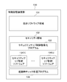
- FIG. 2 is a diagram showing an example of data stored in the auxiliary storage device unit 130.
- the auxiliary storage device unit 130 has an existing software area 131 for storing a system program, an application program, and the like executed by the control unit 100, which will be described later.
- the auxiliary storage device unit 130 has a security area 132 that stores security chip control software 134 (1) -134 (n) that executes each of the n security chips included in the encryption device unit 140 described later.
- Each of the security chip control softwares 134 (1) to 134 (n) executes one of the n security chips as the encryption unit included in the encryption device unit 140, which will be described later, to execute the corresponding security chip.
- the encryption processing is realized according to the destination of the control device 10 (for example, any region (country) from the first region (country) to the nth region (country)).
- the auxiliary storage device unit 130 manages each of the software stored in the existing software area 131 and the security chip control software 134 (1) -134 (n) stored in the security area 132 on a file name basis. May be good. By doing so, the auxiliary storage device unit 130 can delete the software instructed to be deleted from the control unit 100, which will be described later, based on the file name. Alternatively, the auxiliary storage device unit 130 manages the addresses of the software stored in the existing software area 131 and the security chip control software 134 (1) -134 (n) stored in the security area 132 on the file system. You may. By doing so, since the auxiliary storage device unit 130 knows in advance the address and range in which each software is stored, the software instructed to be deleted is deleted based on the address from the control unit 100 described later. be able to.
- the auxiliary storage device unit 130 may store the security chip control abstraction program 133 and the startup check processing program 135.
- the security chip (j) (1 ⁇ j ⁇ n) is supported by the abstracted common interface. It is possible to instruct the security chip control software 134 (j) that executes the control to be performed. It should be noted that such an abstraction process is well known to those skilled in the art, and detailed description thereof will be omitted.
- the control unit 100 (specifically, the calculation unit 101) executes the start-up check processing program 135 to execute the check processing such as the configuration and settings of the control device 10.
- the startup check processing function unit startup check processing unit provided by executing the startup check processing program 135 will be described later.
- FIG. 3 is a diagram showing an example of the configuration of the encryption device unit 140.
- the encryption device unit 140 has n fuses 141 (1) -141 (n), n security chips 142 (1) -142 (n), and n as encryption units. It has a switch SW1-SWn, a diode 143, a switch 144, and a power supply 145.
- the power supply 145 may be arranged in one control circuit (not shown).
- the power supply 150 is, for example, an external constant current source that supplies electric power required for each of the security chips 142 (1) to 142 (n) to operate.
- the fuse 141 (1) -141 (n) is connected to each of the security chips 142 (1) -142 (n) and operates as an invalidating unit.
- the security chips 142 (1) to 142 (n) as the encryption unit for example, a security chip TPM (Trusted Platform Module) conforming to the security specifications defined by TCG (Trusted Computing Group) (registered trademark) can be used. Can be applied.
- the security chips 142 (1) to 142 (n) are TPM, but the security chips 142 (1) to 142 (n) are not limited to the TPM.
- the security chips 142 (1) to 142 (n) may be a discrete TPM mounted on a TPM-compliant dedicated chip as an encryption unit, or may be encrypted by the discrete TPM.
- the security chips 142 (1) to 142 (n) may be the firmware TPM executed in the security area inside the microcomputer as the encryption unit, or may be encrypted by the firmware TPM.
- the security chips 142 (1) to 142 (n) may be a discrete IC that does not conform to the TPM standard as an encryption unit, or may be encrypted by the discrete IC.
- the security chips 142 (1) to 142 (n) may be software encrypted by a microcomputer as an encryption unit.
- each security chip 142 (1) -142 (n) designated for each destination is By executing the corresponding security chip control software 134 (1) -134 (n) stored in the security area 132, the encryption process corresponding to each destination can be performed. ..
- the switch SW (1) -SW (n), the diode 143, the switch 144, and the power supply 145 operate as a load circuit based on, for example, a control instruction from the control unit 100 described later. Specifically, when the operation unit 110 receives the designation of the i-region (country) as the destination of the control device 10, for example, the security chip 142 (j) to be invalidated other than the security chip 142 (i). In order to disconnect (j ⁇ i) from the control circuit, the switch SW (i) is turned off based on the control instruction from the control unit 100 described later, and the switches SW (j) other than the switch SW (i) ( j ⁇ i) turns ON. Note that i is an integer from 1 to n.
- the switch 144 when the switch 144 is turned on based on the instruction from the control unit 100 described later, the electric power from the power supply 145 is applied to the fuse 141 (j) (j ⁇ i) other than the fuse 141 (i).
- the fuse 141 (j) other than the fuse 141 (i) is burnt out.
- the security chips 142 (j) other than the security chips 142 (i) are disconnected from the control circuit and invalidated.
- the switch SW (1) -SW (n) and the switch 144 that operate as a load circuit all the security chips 142 (j) (j ⁇ i) other than the security chip 142 (i) are disconnected from the control circuit. If so, it may have a malfunction prevention function that does not perform invalidation processing.
- the timing of the invalidation process can be determined, and the invalidation process is not performed immediately when the power is turned on, so that the destination is erroneously determined. You can avoid that. However, the diode 143 and the switch 144 do not have to be in the load circuit.
- the power supply 145 is a constant current source that supplies the power required to burn off the fuses 141 (1) -141 (n).
- the control unit 100 includes a calculation unit 101, and is, for example, a processor that controls the control device 10 as a whole.
- the control unit 100 is communicably connected to the main storage device unit 120 and the auxiliary storage device unit 130 via a bus (not shown).
- the arithmetic unit 101 reads out the system program and the application program stored in the existing software area 131 of the auxiliary storage device unit 130 via the bus, and controls the entire control device 10 according to the system program and the application program.
- the arithmetic unit 101 connects the security chip control abstraction program 133, the security chip control software 134 (1) -134 (n), and the startup check processing program 135 stored in the auxiliary storage device unit 130 to the bus. It is read through and controls the security process related to the control device 10 according to the system program and the application program.
- the control unit 100 is configured to realize the security chip control abstraction function and the startup check processing function described above.
- the control unit 100 is subject to at least one invalidation target other than the security chip 142 (i) by operating the switch SW (1) -SW (n) arranged in the encryption device unit 140 and the load circuit of the switch 144.
- the security chip 142 (j) (j ⁇ i) is disabled, the security chip control software 134 (j) (j ⁇ i) corresponding to the disabled security chip 142 (j) is installed in the auxiliary storage unit 130. You may want to remove it from.
- the control unit 100 is different from the security chip 142 (i), for example, when the operation unit 110 receives the designation of the i-region (country) as the destination of the control device 10 from the designer of the machine maker or the like.
- the switch SW (i) is turned off and the switches SW other than the switch SW (i) are turned on. Then, the control unit 100 burns out the fuses 141 (j) (j ⁇ i) other than the fuse 141 (i) by turning on the switch 144, and the security chip other than the security chip 142 (i) to be invalidated. 142 (j) is disconnected from the control circuit and invalidated. At that time, the control unit 100 may delete all the security chip control software 134 (j) (j ⁇ i) other than the security chip control software 134 (i) from the auxiliary storage device unit 130.
- the seller of the control device 10 can sell the control device 10 without setting the destination to the machine maker or the like at the time of shipment, and the designer of the machine maker or the like can sell the control device 10 by the time the machine is shipped.
- the control device 10 having only the encryption function for the selected destination can be obtained. Since the security chip 142 (j) (j ⁇ i) to be invalidated is not used by the destination, security chip control software other than the security chip control software 134 (i) including security information unrelated to the destination. By not leaving 134 (j) (j ⁇ i), the risk of being hacked can be reduced.
- security other than the security chip control software 134 (i) can be obtained by deleting the security chip control software 134 (j) (j ⁇ i) other than the security chip control software 134 (i) before shipping to the destination. It is possible to achieve the effect that the chip control software 134 (j) (j ⁇ i) is not affected by the disclosure request or the like by the law of the destination.
- the security chip control software 134 (j) (j ⁇ i) may be deleted by a method known to those skilled in the art after overwriting zero, deleting after overwriting a random number, or the like.
- the designer of the machine maker accidentally turns off the power of the control device 10 while i) is burned out.
- a part of the fuse 141 (j) (j ⁇ i) other than the fuse 141 (i) is not burned out, and a part of the security chip 142 (j) (j ⁇ i) to be invalidated becomes a control circuit. There is a risk of staying connected.
- the control unit 100 may store, for example, the identification information of the security chip 142 (i) corresponding to the destination of the control device 10 in the auxiliary storage device unit 130. By doing so, when the control device 10 is started, the control unit 100 activates the start-up check processing program 135 to obtain the identification information of the security chip 142 (i) stored in the auxiliary storage device unit 130. , Even if it is determined whether or not all the security chips 142 (j) (j ⁇ i) other than the security chip 142 (i) are disconnected from the control circuit based on the known disconnection detection method. good.
- control unit 100 controls each of the security chips 142 (j) (j ⁇ i) to be invalidated other than the security chip 142 (i) by executing the startup check processing program 135. Send a command for.
- the control unit 100 may determine whether or not all of the security chips 142 (j) (j ⁇ i) to be invalidated are disconnected from the control circuit depending on whether or not a response to the control command has been received. .. That is, when the control unit 100 executes the startup check processing program 135 and a correct response is returned from the security chip 142 (j) (j ⁇ i) to be invalidated, the control unit 100 determines that the connection is established and the response is incorrect. If there is no response, it may be determined that the device is disconnected.
- the control device 10 cannot be activated and the security chip 142 (j) to be invalidated (j) ( An alert indicating that j ⁇ i) is not disconnected from the control circuit may be output and displayed on a display (not shown) of the control device 10. After that, for example, the seller of the control device 10 may reset the security chip 142.
- the control unit 100 sets the area (country) left in the first invalidation process as an auxiliary storage device so that the designer of the machine maker does not mistakenly change to a different destination. It may be stored in the unit 130.
- the control unit 100 is trying to set a destination different from the destination set at the first time.
- An alert or the like may be output and displayed on a display (not shown) of the control device 10.
- the control device 10 ensures that the security chip 142 (j) (j ⁇ i) to be invalidated before the control device 10 can be used by the user.
- the security chip control software 134 (j) (j ⁇ i) that can be invalidated and corresponds to the security chip 142 (j) (j ⁇ i) to be invalidated must be reliably deleted from the auxiliary storage unit 130. Can be done.
- FIG. 4 is a flowchart illustrating a process of deleting a security chip that cannot be used by the destination of the control device 10. The flow shown here is executed every time the destination of the control device 10 is specified.
- step S11 the operation unit 110 receives the designation of the destination of the control device 10 based on the input operation by the designer of the machine maker or the like.
- step S12 the control unit 100 disconnects the security chips 142 (j) (j ⁇ i) to be invalidated other than the security chips 142 (i) corresponding to the destination specified in step S11 from the control circuit.
- the switch SW (i) is set to OFF, and the switches SW (j) (j ⁇ i) other than the switch SW (i) are set to ON.
- step S13 the control unit 100 burns out the fuses 141 (j) (j ⁇ i) other than the fuse 141 (i) by turning on the switch 144, and the security chips 142 (j) (j) to be invalidated. ⁇ i) is disconnected from the control circuit.
- step S14 the arithmetic unit 101 deletes the security chip control software 134 (j) corresponding to the security chip 142 (j) to be invalidated from the auxiliary storage device unit 130.
- FIG. 5 is a flowchart illustrating a deletion process at the time of starting the control device 10. The flow shown here is executed every time the control device 10 is started.
- step S21 the control unit 100 executes the startup check processing program 135 to execute all the security chips 142 (j) (j ⁇ i) to be invalidated except for the destination security chip 142 (i) at startup. Determines if is disconnected from the control circuit. If all of the security chips 142 (j) (j ⁇ i) to be invalidated are disconnected from the control circuit, the process proceeds to step S23. On the other hand, if all of the security chips 142 (j) (j ⁇ i) to be invalidated are not disconnected from the control circuit, the process proceeds to step S22.
- step S22 the control unit 100 disables the control device 10 and outputs an alert indicating that the security chip 142 (j) (j ⁇ i) to be invalidated is not disconnected from the control circuit. , Displayed on a display (not shown) to end the startup process.
- step S23 the control unit 100 performs a normal activation process of the control device 10.
- the control device 10 of one embodiment has in advance security chips 142 (1) -142 (n) having an encryption function corresponding to each of a plurality of regions.
- the control device 10 receives the designation of the destination of the control device 10 based on the input operation by the designer of the machine maker or the like, the control device 10 is an invalidation target other than the security chip 142 (i) corresponding to the designated destination.
- the security chip 142 (j) (j ⁇ i) can be invalidated by disconnecting the security chip 142 (j) (j ⁇ i) from the control circuit.
- the inventory cost can be reduced without preparing the control device 10 for each destination in advance.
- the seller of the control device 10 does not need to prepare inventory for each destination, and the inventory cost of the seller of the control device 10 can be reduced. Further, the machine maker and the production system integrator do not need to prepare the inventory of the control device 10 for each destination, and the inventory cost can be reduced. Further, the control device 10 has a risk of being hacked by deleting all the security chip control software 134 (j) (j ⁇ i) corresponding to the security chip 142 (j) (j ⁇ i) to be invalidated. Can be reduced.
- the control device 10 determines whether or not all the security chips 142 (j) (j ⁇ i) to be invalidated other than the security chip 142 (i) corresponding to the destination are disconnected from the control circuit. judge. Then, the control device 10 makes it impossible to start the control device 10 when all the security chips 142 (j) (j ⁇ i) to be invalidated are not disconnected, and the security chip 142 (j) to be invalidated. ) An alert indicating that (j ⁇ i) is not disconnected from the control circuit may be displayed on a display (not shown) of the control device 10. By doing so, for example, the seller of the control device 10 may reset the security chip 142.
- control device 10 is not limited to the above-described embodiment, and includes deformation, improvement, and the like within a range in which the object can be achieved.
- the encryption device unit 140 has a configuration as shown in FIG. 3, but is not limited thereto.
- FIG. 6 is a diagram showing a configuration example of the encryption device unit 140. The elements having the same functions as the elements of the encryption device unit 140 in FIG. 3 are designated by the same reference numerals, and detailed description thereof will be omitted. As shown in FIG. 6, each of the fuses 141 (1) -141 (n), each of the switches SW (1) -SW (n), and each of the security chips 142 (1) -142 (n) are Connected in series.
- the switch SW (i) is turned off and the switch SW (i) is turned off as in the case of FIG.
- the security chip 142 to be invalidated other than the security chip 142 (i) may be disconnected from the control circuit.
- the control unit 100 executes the startup check processing program 135 to invalidate the security chips 142 (j) other than the destination security chip 142 (i) at startup (j) ( j ⁇ i) If not all are disconnected from the control circuit, an alert indicating that the security chips 142 (j) (j ⁇ i) to be invalidated are not disconnected from the control circuit is output, and the control device 10 outputs the alert. Displayed on a display (not shown), but is not limited to this.
- the control unit 100 disconnects all the security chips 142 (j) (j ⁇ i) to be invalidated again from the control circuit by executing the startup check processing program 135 when the control device 10 is restarted. You may do so. Further, the control unit 100 may delete the security chip control software 134 (j) (j ⁇ i) corresponding to the security chip 142 (j) (j ⁇ i) to be invalidated from the auxiliary storage device unit 130. .. By doing so, the control device 10 can reliably invalidate all the security chips 142 (j) (j ⁇ i) to be invalidated except the security chip 142 (i), and the security chip to be invalidated can be reliably disabled. All of the security chip control software 134 (j) (j ⁇ i) corresponding to 142 (j) (j ⁇ i) can be reliably deleted from the auxiliary storage device unit 130.
- Each function included in the control device 10 according to the embodiment can be realized by hardware, software, or a combination thereof.
- what is realized by software means that it is realized by a computer reading and executing a program.
- each component included in the control device 10 can be realized by hardware, software including an electronic circuit or the like, or a combination thereof.
- Non-transitory computer-readable media include various types of tangible recording media (Tangible storage media).
- Examples of non-temporary computer-readable media include magnetic recording media (eg, flexible disks, magnetic tapes, hard disk drives), magneto-optical recording media (eg, magneto-optical disks), CD-ROMs (Read Only Memory), and CD-.
- the program may also be supplied to the computer by various types of temporary computer-readable media (Transity computer readable medium).
- temporary computer-readable media include electrical, optical, and electromagnetic waves.
- the temporary computer-readable medium can supply the program to the computer via a wired communication path such as an electric wire and an optical fiber, or a wireless communication path.
- the step of describing the program to be recorded on the recording medium is not only the processing performed in chronological order but also the processing executed in parallel or individually even if it is not necessarily processed in chronological order. Also includes.
- control device of the present disclosure can take various embodiments having the following configurations.
- the control device 10 of the present disclosure is a control device that controls an industrial machine and includes an encryption unit, and has either a plurality of security chips 142 or a plurality of security chips 142 corresponding to a plurality of destinations.
- An encryption device unit 140 including a plurality of invalidation units for invalidating or disabling a plurality of security chips 142, and a plurality of security chips 142 for each of the plurality of invalidation units depending on the destination of the control device 10.
- the operation unit 110 is provided with an operation unit 110 for specifying whether to invalidate any of the security chips 142 or invalidating the plurality of security chips 142 and selecting the invalidation of the security chips 142. According to this control device 10, inventory cost can be reduced without preparing a control device 10 for each destination in advance.
- the security chips 142 (1) -142 (n) are executed at least in the TPM, the discrete TPM mounted by the TPM-compliant dedicated chip, and the security area inside the microcomputer. It may be a security chip of either a firmware TPM or a discrete IC that does not conform to the TPM standard. By doing so, the control device 10 can use the desired security chip.
- the invalidation unit is the fuse 141 (1) -141 (n)
- the encryption device unit 140 is the security chip 142 corresponding to the destination.
- a load circuit for operating the fuse 141 (j) (j ⁇ i) so as to invalidate the security chip 142 (j) (j ⁇ i) to be invalidated other than (1) may be provided. By doing so, the control device 10 can surely disconnect the security chip 142 (j) (j ⁇ i) to be invalidated.
- a plurality of security chip control software 134 (1) -134 (n) for controlling the operation of each of the plurality of security chips 142 (1) -142 (n) is used.
- the security chip control corresponding to the disabled security chip 142 is invalidated by the auxiliary storage unit 130 for storage and the fuse 141 (1) -141 (n)
- a calculation unit 101 that deletes the software 134 from the auxiliary storage device unit 130 may be provided. By doing so, the control device 10 can reduce the risk of being hacked.
- the control device 10 at the time of startup, when the control device 10 is started, it is determined whether or not all of the security chips 142 (j) (j ⁇ i) to be invalidated are disabled. Further, the calculation unit 101 further includes a check processing unit, and when it is determined by the startup check processing unit that all of the security chips 142 (j) (j ⁇ i) to be invalidated are not invalidated, the calculation unit 101 is subject to invalidation. An alert may be output indicating that all of the security chips 142 (j) (j ⁇ i) have not been disabled. By doing so, the control device 10 can reliably disable all the security chips 142 (j) (j ⁇ i) to be invalidated before the control device 10 becomes available to the user.
- control device 10 when it is determined by the start-up check processing unit that all of the security chips 142 (j) (j ⁇ i) to be invalidated have been invalidated. , It may have a malfunction prevention function that does not perform invalidation processing. By doing so, the control device 10 can safely invalidate all the security chips 142 to be invalidated.
- the calculation unit 101 stores the destination of the control device 10 in the auxiliary storage device unit 130
- the operation unit 110 stores the destination of the control device 10 in the auxiliary storage device unit 130.
- an alert indicating that the destination is different from the destination stored in the auxiliary storage device 130 may be output.
- Control device 100 Control unit 101 Calculation unit 110 Operation unit 120 Main storage unit 130 Auxiliary storage unit 131 Existing software area 132 Security area 134 (1) -134 (n) Security chip control software 135 Startup check processing program 140 Encryption Software unit 141 (1) -141 (n) Hughes 142 (1) -142 (n) Security chip SW (1) -SW (n) 144 switches
Landscapes
- Engineering & Computer Science (AREA)
- Computer Security & Cryptography (AREA)
- Theoretical Computer Science (AREA)
- Software Systems (AREA)
- Computer Hardware Design (AREA)
- General Engineering & Computer Science (AREA)
- General Physics & Mathematics (AREA)
- Physics & Mathematics (AREA)
- Signal Processing (AREA)
- Computer Networks & Wireless Communication (AREA)
- Health & Medical Sciences (AREA)
- Bioethics (AREA)
- General Health & Medical Sciences (AREA)
- Stored Programmes (AREA)
- Numerical Control (AREA)
- Storage Device Security (AREA)
Abstract
Description
一方で、制御装置の販売者は販売する同じ制御装置の暗号技術に関しては仕向け先国(地域)それぞれの法規に従う必要があり、加えて、ある仕向け先国(地域)に対応できる暗号技術を使用可能な状態で別の仕向け国(地域)に販売できない法規もあることから、一種類の暗号化チップでは、すべての仕向け先国(地域)の法規を満たせない場合がある。
そのため、制御装置の販売者は、仕向け先の国(地域)毎に適切な暗号化チップを使う必要等があるため、国(地域)毎に異なる暗号化チップを実装した制御装置を複数用意する必要がある。
また、制御装置を工作機械や生産システムに組み込んで商品開発する機械メーカは、それぞれ異なる国に出荷する場合に、それぞれの国に対応した暗号化チップを実装した制御装置の在庫を持つ必要があり、機械メーカにとっても在庫コスト(製造コスト)がかかるという問題もある。
図1は、一実施形態に係る制御装置の機能的構成例を示す機能ブロック図である。
制御装置10は、当業者にとって公知の数値制御装置であり、制御情報に基づいて動作指令を生成し、生成した動作指令を工作機械(図示しない)に出力する。これにより、制御装置10は、工作機械(図示しない)の動作を制御する。なお、工作機械(図示しない)がロボット等の場合、制御装置1は、ロボット制御装置等でもよい。
操作部110は、例えば、制御装置10に含まれる図示しないMDIユニットのキーボードや表示器のタッチパネルあるいは物理的なロータリスイッチ等であり、制御装置10の販売者や機械メーカの設計者等からの操作を受け付ける。
具体的には、操作部110は、機械メーカの設計者等による操作に基づいて、制御装置10の仕向け先の指定を受け付け、受け付けた仕向け先に応じて後述する暗号化装置部140に含まれるn個のセキュリティチップのうち無効化対象のセキュリティチップを指定する(nは2以上の整数)。
なお、後述する補助記憶装置部130が、例えば、暗号化装置部140のn個のセキュリティチップそれぞれと仕向け先とを対応付けした仕向け先テーブル(図示しない)を予め記憶し、操作部110が制御装置10の仕向け先の指定を受け付け、指定された仕向け先に対応する有効のままとするセキュリティチップを選択した場合、後述する制御部100は、選択されたセキュリティチップと仕向け先テーブル(図示しない)とに基づいて、無効化対象のセキュリティチップを判定するようにしてもよい。
主記憶装置部120は、例えば、RAM(Random Access Memory)等のメモリであり、後述する制御部100がプログラムを実行する上で一時的に必要とされるデータを格納する。
補助記憶装置部130は、例えば、ROM(Read Only Memory)やHDD(Hard Disk Drive)やフラッシュメモリ等である。
図2は、補助記憶装置部130に格納されるデータの一例を示す図である。
図2に示すように、補助記憶装置部130は、後述する制御部100が実行するシステムプログラム及びアプリケーションプログラム等を格納する既存ソフトウェア領域131を有する。また、補助記憶装置部130は、後述する暗号化装置部140に含まれるn個のセキュリティチップそれぞれを実行するセキュリティチップ制御ソフトウェア134(1)-134(n)を格納するセキュリティ領域132を有する。
セキュリティチップ制御ソフトウェア134(1)-134(n)それぞれは、後述する暗号化装置部140に含まれる暗号化部としてのn個のセキュリティチップのうち対応する1つのセキュリティチップを実行することにより、制御装置10の仕向け先(例えば、第1地域(国)から第n地域(国)のいずれかの地域(国))に応じた暗号化処理を実現する。
後述する制御部100(具体的には演算部101)によりセキュリティチップ制御抽象化プログラム133を実行することにより、抽象化された共通インタフェースにより、セキュリティチップ(j)(1≦j≦n)に対応する制御を実行するセキュリティチップ制御ソフトウェア134(j)に対して、指示することを可能とする。なお、このような抽象化処理は、当業者に取って公知であり、詳細な説明は省略する。
また、制御装置10の起動時に、制御部100(具体的には演算部101)により起動時チェック処理プログラム135を実行することにより、制御装置10の構成や設定等のチェック処理を実行する。なお、起動時チェック処理プログラム135を実行することにより提供される起動時チェック処理機能部(起動時チェック処理部)については後述する。
図3は、暗号化装置部140の構成の一例を示す図である。
図3に示すように、暗号化装置部140は、暗号化部として、n個のヒューズ141(1)-141(n)、n個のセキュリティチップ142(1)-142(n)、n個のスイッチSW1-SWn、ダイオード143、スイッチ144、及び電源145を有する。n個のヒューズ141(1)-141(n)、n個のセキュリティチップ142(1)-142(n)、n個のスイッチSW(1)-SW(n)、ダイオード143、スイッチ144、及び電源145は、図示しない1つの制御回路に配置されてもよい。
なお、電源150は、例えば、セキュリティチップ142(1)-142(n)それぞれが動作するのに必要な電力を供給する、外部の定電流源である。
前述したように、例えば仕向け先(第1地域(国)から第n地域(国)のいずれかの地域(国))毎に指定されるそれぞれのセキュリティチップ142(1)-142(n)は、セキュリティ領域132に格納された、対応するそれぞれのセキュリティチップ制御ソフトウェア134(1)-134(n)を実行することにより、仕向け先に特化したそれぞれに対応した暗号化処理を行うことができる。
具体的には、操作部110が、例えば、制御装置10の仕向け先として第i地域(国)の指定を受け付けた場合、セキュリティチップ142(i)以外の無効化対象のセキュリティチップ142(j)(j≠i)を制御回路から切断するために、後述する制御部100からの制御指示に基づいて、スイッチSW(i)はOFFになり、スイッチSW(i)以外のスイッチSW(j)(j≠i)はONになる。なお、iは1からnの整数である。この場合、後述する制御部100からの指示に基づきスイッチ144がONになると、電源145からの電力がヒューズ141(i)以外のヒューズ141(j)(j≠i)に印加されることで、ヒューズ141(i)以外のヒューズ141(j)が焼き切られる。これにより、セキュリティチップ142(i)以外のセキュリティチップ142(j)が制御回路から切断され無効化される。
なお、加負荷回路として動作するスイッチSW(1)-SW(n)及びスイッチ144は、セキュリティチップ142(i)以外のセキュリティチップ142(j)(j≠i)全てが制御回路から切断されている場合、無効化処理を行わない誤作動防止機能を有してもよい。
また、加負荷回路としてのダイオード143及びスイッチ144があることにより、無効化処理のタイミングを決定することができ、電源投入時にすぐに無効化処理にならないことで、誤って仕向け先が決まってしまうことを避けることができる。ただし、ダイオード143及びスイッチ144は加負荷回路になくてもよい。
制御部100は、演算部101を備え、例えば制御装置10を全体的に制御するプロセッサである。制御部100は、図示しないバスを介して主記憶装置部120、及び補助記憶装置部130と通信可能に接続される。
演算部101は、補助記憶装置部130の既存ソフトウェア領域131に格納されたシステムプログラム及びアプリケーションプログラムを、バスを介して読み出し、前記システムプログラム及びアプリケーションプログラムに従って制御装置10全体を制御する。
同様に、演算部101は、補助記憶装置部130に格納されたセキュリティチップ制御抽象化プログラム133、セキュリティチップ制御ソフトウェア134(1)-134(n)、及び起動時チェック処理プログラム135を、バスを介して読み出し、前記システムプログラム及びアプリケーションプログラムに従って、制御装置10に係るセキュリティ処理を制御する。
これにより、図1に示すように、制御部100は、前述したセキュリティチップ制御抽象化機能、及び起動時チェック処理機能を実現するように構成される。
具体的には、制御部100は、例えば、操作部110が制御装置10の仕向け先として第i地域(国)の指定を機械メーカの設計者等から受け付けた場合、セキュリティチップ142(i)以外のセキュリティチップ142を制御回路から切断するために、スイッチSW(i)をOFFにし、スイッチSW(i)以外のスイッチSWをONにする。そして、制御部100は、スイッチ144をONにすることで、ヒューズ141(i)以外のヒューズ141(j)(j≠i)を焼き切り、セキュリティチップ142(i)以外の無効化対象のセキュリティチップ142(j)を制御回路から切断し無効化する。その際、制御部100は、セキュリティチップ制御ソフトウェア134(i)以外のセキュリティチップ制御ソフトウェア134(j)(j≠i)全てを補助記憶装置部130から削除するようにしてもよい。
なお、無効化対象のセキュリティチップ142(j)(j≠i)は仕向け先では使われないため、仕向け先とは関係ないセキュリティ情報を含むセキュリティチップ制御ソフトウェア134(i)以外のセキュリティチップ制御ソフトウェア134(j)(j≠i)を残さないようにすることで、ハッキングされるリスクを減らすことができる。また、仕向け先への出荷前に、セキュリティチップ制御ソフトウェア134(i)以外のセキュリティチップ制御ソフトウェア134(j)(j≠i)を削除することによって、セキュリティチップ制御ソフトウェア134(i)以外のセキュリティチップ制御ソフトウェア134(j)(j≠i)が仕向け先の法律による開示要求等の影響を受けずに済むという効果を奏することができる。
なお、セキュリティチップ制御ソフトウェア134(j)(j≠i)の削除は、当業者にとって公知のゼロ上書き後削除や、乱数上書き後削除等で行われてもよい。
具体的には、制御部100は、起動時チェック処理プログラム135を実行することで、例えば、セキュリティチップ142(i)以外の無効化対象のセキュリティチップ142(j)(j≠i)それぞれに制御用コマンドを送信する。制御部100は、前記制御用コマンドに対する応答を受けたか否かで、無効化対象のセキュリティチップ142(j)(j≠i)全てが制御回路から切断されているか否かを判定してもよい。すなわち、制御部100は、起動時チェック処理プログラム135を実行することで、無効化対象のセキュリティチップ142(j)(j≠i)から正しい応答が帰る場合、接続と判定し、正しくない応答若しくは応答がない場合、切断されていると判定するようにしてもよい。
ただし、一度無効化処理を実行した場合、機械メーカの設計者等が誤って違う仕向け先に変えないように、制御部100は、一度目の無効化処理で残す地域(国)を補助記憶装置部130に記憶してもよい。そして、機械メーカの設計者等が一度目に設定した仕向け先と違う仕向け先を設定しようとした場合、制御部100は、一度目に設定した仕向け先と違う仕向け先を設定しようとしていることを示すアラート等を出力し、制御装置10の図示しない表示器に表示するようにしてもよい。
そうすることで、制御装置10は、仕向け先が一度指定されると、ユーザにより制御装置10が使用可能となる前に、無効化対象のセキュリティチップ142(j)(j≠i)を確実に無効化することができ、無効化対象のセキュリティチップ142(j)(j≠i)に対応するセキュリティチップ制御ソフトウェア134(j)(j≠i)を補助記憶装置部130から確実に削除することができる。
次に、本実施形態に係る制御装置10の削除処理に係る動作について説明する。
図4は、制御装置10の仕向け先で使用不可のセキュリティチップの削除処理について説明するフローチャートである。ここで示すフローは、制御装置10の仕向け先が指定される度に実行される。
次に、本実施形態に係る制御装置10の起動時の処理に係る動作について説明する。
図5は、制御装置10の起動時の削除処理について説明するフローチャートである。ここで示すフローは、制御装置10が起動される度に実行される。
これにより、仕向け先毎の制御装置10を予め用意することなく、在庫コストを低減することができる。すなわち、制御装置10の販売者は、仕向け先毎に在庫を用意する必要がなくなり、制御装置10の販売者の在庫コストを低減することができる。また、機械メーカや生産システムインテグレータは、仕向け先毎に制御装置10の在庫を用意する必要がなくなり、在庫コストを低減することができる。
また、制御装置10は、無効化対象のセキュリティチップ142(j)(j≠i)に対応するセキュリティチップ制御ソフトウェア134(j)(j≠i)全てを削除することにより、ハッキングされるリスクを減らすことができる。
また、制御装置10は、起動時に、仕向け先に対応するセキュリティチップ142(i)以外の無効化対象のセキュリティチップ142(j)(j≠i)全てが制御回路から切断されているか否かを判定する。そして、制御装置10は、無効化対象のセキュリティチップ142(j)(j≠i)全てが切断されていない場合、制御装置10を起動できないようにするとともに、無効化対象のセキュリティチップ142(j)(j≠i)が制御回路から切断されていないことを示すアラートを、制御装置10の図示しない表示器に表示してもよい。そうすることで、例えば、制御装置10の販売者等により、セキュリティチップ142の再設定を行うようにしてもよい。
上述の実施形態では、暗号化装置部140は、図3に示すような構成を有したが、これに限定されない。
図6は、暗号化装置部140の構成例を示す図である。なお、図3の暗号化装置部140の要素と同様の機能を有する要素については、同じ符号を付し、詳細な説明は省略する。
図6に示すように、ヒューズ141(1)-141(n)それぞれと、スイッチSW(1)-SW(n)のそれぞれと、セキュリティチップ142(1)-142(n)のそれぞれと、が直列に接続される。そして、演算部101は、例えば、制御装置10の仕向け先として第i地域(国)の指定を受け付けた場合、図3の場合と同様に、スイッチSW(i)をOFFにし、スイッチSW(i)以外のスイッチSWをONにすることにより、セキュリティチップ142(i)以外の無効化対象のセキュリティチップ142を制御回路から切断してもよい。
また例えば、上述の実施形態では、制御部100は、起動時チェック処理プログラム135を実行することで、起動時に仕向け先のセキュリティチップ142(i)以外の無効化対象のセキュリティチップ142(j)(j≠i)全てが制御回路から切断されていない場合、無効化対象のセキュリティチップ142(j)(j≠i)が制御回路から切断されていないことを示すアラートを出力し、制御装置10の図示しない表示器に表示したが、これに限定されない。
例えば、制御部100は、制御装置10の再起動時に、起動時チェック処理プログラム135を実行することで、再度無効化対象のセキュリティチップ142(j)(j≠i)全てを制御回路から切断するようにしてもよい。また、制御部100は、無効化対象のセキュリティチップ142(j)(j≠i)に対応するセキュリティチップ制御ソフトウェア134(j)(j≠i)を補助記憶装置部130から削除してもよい。
そうすることで、制御装置10は、セキュリティチップ142(i)以外の無効化対象のセキュリティチップ142(j)(j≠i)全てを確実に無効化することができ、無効化対象のセキュリティチップ142(j)(j≠i)に対応するセキュリティチップ制御ソフトウェア134(j)(j≠i)全てを補助記憶装置部130から確実に削除することができる。
また、制御装置10に含まれる各構成部は、電子回路等を含むハードウェア、ソフトウェア又はこれらの組み合わせにより実現することができる。
この制御装置10によれば、仕向け先毎の制御装置10を予め用意することなく、在庫コストを低減することができる。
そうすることで、制御装置10は、所望のセキュリティチップを使用することができる。
そうすることで、制御装置10は、無効化対象のセキュリティチップ142(j)(j≠i)を確実に切断することができる。
そうすることで、制御装置10は、ハッキングされるリスクを減らすことができる。
そうすることで、制御装置10は、ユーザにより制御装置10が使用可能となる前に、無効化対象のセキュリティチップ142(j)(j≠i)全てを確実に無効化することができる。
そうすることで、制御装置10は、無効化対象のセキュリティチップ142全てを安全に無効化することができる。
そうすることで、制御装置10は、機械メーカの設計者等が一度設定した仕向け先を再度仕向け先を変えようとした場合、既に仕向け先が設定されている旨を機械メーカの設計者等に通知することができる。
100 制御部
101 演算部
110 操作部
120 主記憶装置部
130 補助記憶装置部
131 既存ソフトウェア領域
132 セキュリティ領域
134(1)-134(n) セキュリティチップ制御ソフトウェア
135 起動時チェック処理プログラム
140 暗号化装置部
141(1)-141(n) ヒューズ
142(1)-142(n) セキュリティチップ
SW(1)-SW(n)、144 スイッチ
Claims (7)
- 産業機械を制御し暗号化部を含む制御装置であって、
複数の仕向け先毎に対応した複数の前記暗号化部と複数の前記暗号化部のいずれかを無効化するもしくは複数の前記暗号化部を無効化する複数の無効化部とを含む暗号化装置部と、
前記制御装置の仕向け先に応じて前記複数の無効化部それぞれに複数の前記暗号化部のいずれかを無効化させるか複数の前記暗号化部を無効化させるかを指定して、暗号化部の無効化を選択する操作部と、
を備える制御装置。 - 前記暗号化部は、少なくともTPM(Trusted Platform Module)、TPM準拠の専用チップで実装されたディスクリートTPM、マイコン内部のセキュリティ領域で実行されるファームウェアTPM、又はTPM規格に準拠しないディスクリートICのいずれかのセキュリティチップである、請求項1に記載の制御装置。
- 前記無効化部はヒューズであり、
前記暗号化装置部は、
前記仕向け先に対応する暗号化部以外の無効化対象の暗号化部を無効化するように前記無効化部を動作させる加負荷回路を備える、請求項1又は請求項2に記載の制御装置。 - 前記複数の暗号化部の各々の動作を制御する複数の制御ソフトウェアを記憶する補助記憶装置部と、
前記無効化部により少なくとも1つの無効化対象の暗号化部が無効化された場合、無効化された前記無効化対象の暗号化部に対応する制御ソフトウェアを前記補助記憶装置部から削除する演算部と、を備える、請求項3に記載の制御装置。 - 前記制御装置の起動時に、前記無効化対象の暗号化部全てが無効化されているか否かを判定する起動時チェック処理部をさらに備え、
前記演算部は、前記起動時チェック処理部により前記無効化対象の暗号化部全てが無効化されていないと判定された場合、前記無効化対象の暗号化部全てが無効化されていないことを示すアラートを出力する、請求項4に記載の制御装置。 - 前記加負荷回路は、前記起動時チェック処理部により前記無効化対象の暗号化部全てが無効化されたと判定された場合、無効化処理を行わない誤作動防止機能を有する、請求項5に記載の制御装置。
- 前記演算部は、前記制御装置の仕向け先を前記補助記憶装置部に記憶し、前記操作部が前記補助記憶装置部に記憶された仕向け先と異なる仕向け先を受け付けた場合、前記補助記憶装置部に記憶された仕向け先と異なることを示すアラートを出力する、請求項4から請求項6のいずれか1項に記載の制御装置。
Priority Applications (4)
| Application Number | Priority Date | Filing Date | Title |
|---|---|---|---|
| DE112021003462.6T DE112021003462T5 (de) | 2020-06-30 | 2021-06-24 | Steuervorrichtung |
| JP2022533929A JP7392152B2 (ja) | 2020-06-30 | 2021-06-24 | 制御装置 |
| CN202180046116.7A CN115997181B (zh) | 2020-06-30 | 2021-06-24 | 控制装置 |
| US18/010,117 US12368594B2 (en) | 2020-06-30 | 2021-06-24 | Control device |
Applications Claiming Priority (2)
| Application Number | Priority Date | Filing Date | Title |
|---|---|---|---|
| JP2020112468 | 2020-06-30 | ||
| JP2020-112468 | 2020-06-30 |
Publications (1)
| Publication Number | Publication Date |
|---|---|
| WO2022004544A1 true WO2022004544A1 (ja) | 2022-01-06 |
Family
ID=79316188
Family Applications (1)
| Application Number | Title | Priority Date | Filing Date |
|---|---|---|---|
| PCT/JP2021/023913 Ceased WO2022004544A1 (ja) | 2020-06-30 | 2021-06-24 | 制御装置 |
Country Status (5)
| Country | Link |
|---|---|
| US (1) | US12368594B2 (ja) |
| JP (1) | JP7392152B2 (ja) |
| CN (1) | CN115997181B (ja) |
| DE (1) | DE112021003462T5 (ja) |
| WO (1) | WO2022004544A1 (ja) |
Cited By (1)
| Publication number | Priority date | Publication date | Assignee | Title |
|---|---|---|---|---|
| JP2022114391A (ja) * | 2021-01-26 | 2022-08-05 | 京セラドキュメントソリューションズ株式会社 | 電子機器 |
Citations (2)
| Publication number | Priority date | Publication date | Assignee | Title |
|---|---|---|---|---|
| JP2010098367A (ja) * | 2008-10-14 | 2010-04-30 | Sony Corp | 情報処理装置、暗号切替方法、及びプログラム |
| WO2021019637A1 (ja) * | 2019-07-29 | 2021-02-04 | オムロン株式会社 | セキュリティ装置、サーバ装置、セキュリティシステム、及びセキュリティ機能設定方法 |
Family Cites Families (11)
| Publication number | Priority date | Publication date | Assignee | Title |
|---|---|---|---|---|
| CA2242777A1 (en) * | 1996-01-10 | 1997-07-17 | John Griffits | A secure pay-as-you-use system for computer software |
| JP2812312B2 (ja) * | 1996-01-12 | 1998-10-22 | 三菱電機株式会社 | 暗号化システム |
| JP4629416B2 (ja) * | 2003-11-28 | 2011-02-09 | パナソニック株式会社 | データ処理装置 |
| US20060059372A1 (en) * | 2004-09-10 | 2006-03-16 | International Business Machines Corporation | Integrated circuit chip for encryption and decryption having a secure mechanism for programming on-chip hardware |
| JP4596256B2 (ja) * | 2005-08-02 | 2010-12-08 | ソニー株式会社 | 送受信システムおよび方法、送信装置および方法、受信装置および方法、並びにプログラム |
| JP5545026B2 (ja) | 2010-05-18 | 2014-07-09 | Dmg森精機株式会社 | 電子機器、および制限解除方法 |
| JP2012084043A (ja) * | 2010-10-14 | 2012-04-26 | Hagiwara Solutions Co Ltd | 暗号化記憶装置、情報機器、暗号化記憶装置のセキュリティ方法 |
| US9037854B2 (en) * | 2013-01-22 | 2015-05-19 | Amazon Technologies, Inc. | Privileged cryptographic services in a virtualized environment |
| JP5832563B2 (ja) | 2014-01-24 | 2015-12-16 | ファナック株式会社 | 外部プログラム呼び出しできる数値制御装置 |
| US20160378686A1 (en) * | 2015-06-24 | 2016-12-29 | Intel Corporation | Memory encryption exclusion method and apparatus |
| CN110795774B (zh) * | 2018-08-02 | 2023-04-11 | 阿里巴巴集团控股有限公司 | 基于可信高速加密卡的度量方法、设备和系统 |
-
2021
- 2021-06-24 US US18/010,117 patent/US12368594B2/en active Active
- 2021-06-24 DE DE112021003462.6T patent/DE112021003462T5/de active Pending
- 2021-06-24 JP JP2022533929A patent/JP7392152B2/ja active Active
- 2021-06-24 CN CN202180046116.7A patent/CN115997181B/zh active Active
- 2021-06-24 WO PCT/JP2021/023913 patent/WO2022004544A1/ja not_active Ceased
Patent Citations (2)
| Publication number | Priority date | Publication date | Assignee | Title |
|---|---|---|---|---|
| JP2010098367A (ja) * | 2008-10-14 | 2010-04-30 | Sony Corp | 情報処理装置、暗号切替方法、及びプログラム |
| WO2021019637A1 (ja) * | 2019-07-29 | 2021-02-04 | オムロン株式会社 | セキュリティ装置、サーバ装置、セキュリティシステム、及びセキュリティ機能設定方法 |
Cited By (1)
| Publication number | Priority date | Publication date | Assignee | Title |
|---|---|---|---|---|
| JP2022114391A (ja) * | 2021-01-26 | 2022-08-05 | 京セラドキュメントソリューションズ株式会社 | 電子機器 |
Also Published As
| Publication number | Publication date |
|---|---|
| CN115997181B (zh) | 2025-10-14 |
| US20230353370A1 (en) | 2023-11-02 |
| JPWO2022004544A1 (ja) | 2022-01-06 |
| DE112021003462T5 (de) | 2023-04-13 |
| JP7392152B2 (ja) | 2023-12-05 |
| CN115997181A (zh) | 2023-04-21 |
| US12368594B2 (en) | 2025-07-22 |
Similar Documents
| Publication | Publication Date | Title |
|---|---|---|
| US8713296B2 (en) | Apparatus for restoring setting information of a board management controller from a backup memory before loading an OS when a system board is replaced | |
| TWI475402B (zh) | 遠端備份系統及其遠端備份方法 | |
| JP6585072B2 (ja) | 不揮発性メモリ又はセキュア素子へのデータの読み込みを安全に行うこと | |
| JP7026089B2 (ja) | セキュリティシステムおよびコンピュータプログラム | |
| TWI740158B (zh) | 伺服器系統、集中式快閃記憶體模組以及更新快閃韌體映像檔的方法 | |
| JP6541177B2 (ja) | コンピュータ端末及びそのプログラム、コンピュータシステム | |
| JP6199796B2 (ja) | 設定更新方法及び画像形成装置 | |
| CN111209606A (zh) | 一种预警raid卡后硬盘变动的方法、装置和设备 | |
| CN109343867B (zh) | 软件自助安装方法、装置、计算机设备及存储介质 | |
| JP7392152B2 (ja) | 制御装置 | |
| CN102763046B (zh) | 可编程控制器 | |
| JP6680741B2 (ja) | 数値制御装置 | |
| WO2007088605A1 (ja) | 部品情報復元方法、部品情報管理方法及び電子装置 | |
| US6728889B1 (en) | Password recognition circuit and security checking method | |
| JP6657166B2 (ja) | ストレージ制御装置およびストレージ制御方法 | |
| US8898781B2 (en) | Communications system having security apparatus, security apparatus and method herefor | |
| WO2024244436A1 (zh) | 程序启动方法、装置、服务器及非易失性可读存储介质 | |
| KR20180020088A (ko) | 데이터 보호를 위한 백업 솔루션 모듈, 시스템 및 그 구동방법 | |
| CN113626792A (zh) | PCIe Switch固件安全执行方法、装置、终端及存储介质 | |
| CN111783162A (zh) | 数据保护实现方法、装置及计算机设备 | |
| JP5439736B2 (ja) | コンピュータ管理システム、コンピュータシステムの管理方法、及びコンピュータシステムの管理プログラム | |
| JP7341376B2 (ja) | 情報処理装置、情報処理方法、及び、情報処理プログラム | |
| JP6656320B2 (ja) | 工作機械の制御装置 | |
| JPH1049494A (ja) | 作業装置及びプログラムのプロテクト方法 | |
| JP6008400B2 (ja) | 情報処理装置、情報処理装置の制御方法、プログラム及び保守管理システム |
Legal Events
| Date | Code | Title | Description |
|---|---|---|---|
| 121 | Ep: the epo has been informed by wipo that ep was designated in this application |
Ref document number: 21834481 Country of ref document: EP Kind code of ref document: A1 |
|
| ENP | Entry into the national phase |
Ref document number: 2022533929 Country of ref document: JP Kind code of ref document: A |
|
| 122 | Ep: pct application non-entry in european phase |
Ref document number: 21834481 Country of ref document: EP Kind code of ref document: A1 |
|
| WWG | Wipo information: grant in national office |
Ref document number: 202180046116.7 Country of ref document: CN |