WO2022004401A1 - 集束イオンビーム装置 - Google Patents
集束イオンビーム装置 Download PDFInfo
- Publication number
- WO2022004401A1 WO2022004401A1 PCT/JP2021/022972 JP2021022972W WO2022004401A1 WO 2022004401 A1 WO2022004401 A1 WO 2022004401A1 JP 2021022972 W JP2021022972 W JP 2021022972W WO 2022004401 A1 WO2022004401 A1 WO 2022004401A1
- Authority
- WO
- WIPO (PCT)
- Prior art keywords
- ion beam
- focused ion
- substrate
- beam device
- processed
- Prior art date
- Legal status (The legal status is an assumption and is not a legal conclusion. Google has not performed a legal analysis and makes no representation as to the accuracy of the status listed.)
- Ceased
Links
Images

Classifications
-
- H—ELECTRICITY
- H01—ELECTRIC ELEMENTS
- H01J—ELECTRIC DISCHARGE TUBES OR DISCHARGE LAMPS
- H01J37/00—Discharge tubes with provision for introducing objects or material to be exposed to the discharge, e.g. for the purpose of examination or processing thereof
- H01J37/02—Details
- H01J37/04—Arrangements of electrodes and associated parts for generating or controlling the discharge, e.g. electron-optical arrangement or ion-optical arrangement
- H01J37/06—Electron sources; Electron guns
-
- H—ELECTRICITY
- H01—ELECTRIC ELEMENTS
- H01J—ELECTRIC DISCHARGE TUBES OR DISCHARGE LAMPS
- H01J37/00—Discharge tubes with provision for introducing objects or material to be exposed to the discharge, e.g. for the purpose of examination or processing thereof
- H01J37/02—Details
- H01J37/18—Vacuum locks ; Means for obtaining or maintaining the desired pressure within the vessel
-
- H—ELECTRICITY
- H01—ELECTRIC ELEMENTS
- H01J—ELECTRIC DISCHARGE TUBES OR DISCHARGE LAMPS
- H01J37/00—Discharge tubes with provision for introducing objects or material to be exposed to the discharge, e.g. for the purpose of examination or processing thereof
- H01J37/02—Details
- H01J37/20—Means for supporting or positioning the object or the material; Means for adjusting diaphragms or lenses associated with the support
-
- H—ELECTRICITY
- H01—ELECTRIC ELEMENTS
- H01J—ELECTRIC DISCHARGE TUBES OR DISCHARGE LAMPS
- H01J37/00—Discharge tubes with provision for introducing objects or material to be exposed to the discharge, e.g. for the purpose of examination or processing thereof
- H01J37/02—Details
- H01J37/244—Detectors; Associated components or circuits therefor
-
- H—ELECTRICITY
- H01—ELECTRIC ELEMENTS
- H01J—ELECTRIC DISCHARGE TUBES OR DISCHARGE LAMPS
- H01J37/00—Discharge tubes with provision for introducing objects or material to be exposed to the discharge, e.g. for the purpose of examination or processing thereof
- H01J37/30—Electron-beam or ion-beam tubes for localised treatment of objects
- H01J37/305—Electron-beam or ion-beam tubes for localised treatment of objects for casting, melting, evaporating, or etching
-
- H—ELECTRICITY
- H01—ELECTRIC ELEMENTS
- H01J—ELECTRIC DISCHARGE TUBES OR DISCHARGE LAMPS
- H01J37/00—Discharge tubes with provision for introducing objects or material to be exposed to the discharge, e.g. for the purpose of examination or processing thereof
- H01J37/30—Electron-beam or ion-beam tubes for localised treatment of objects
- H01J37/317—Electron-beam or ion-beam tubes for localised treatment of objects for changing properties of the objects or for applying thin layers thereon, e.g. for ion implantation
Definitions
- the present invention relates to a focused ion beam device.
- the focused ion beam device generates ions in a vacuum and condenses them in an electrostatic field to form a focused ion beam.
- the focused ion beam device captures secondary charged particles (secondary electrons, secondary ions, etc.) generated from the position where the focused ion beam is irradiated, and scans the ion beam based on the intensity information. Get the data as an image. When the intensity information at the beam irradiation position is displayed based on this data, the surface shape of the sample irradiated with the ion beam can be confirmed.
- the focused ion beam device can be used as a correction device such as a photomask.
- the photomask pattern is made of chromium (Cr).
- the defective (black defect) portion of this pattern can be removed by sputtering the pattern by irradiating it with a focused ion beam.
- the focused ion beam device has a function of performing CVD (chemical vapor deposition) using the focused ion beam and the film forming gas.
- the focused ion beam is a unipolar gallium positive ion
- positive charges are accumulated on the sample surface if irradiation is continued.
- the sample itself is an insulator, there is a problem that the surface of the sample is charged up and the focused ion beam to be irradiated is shaken or cannot be irradiated.
- a charged beam processing apparatus including a neutralizing electron gun that emits an electron beam toward the sample surface irradiated with an ion beam is known (for example, Patent Document). 1).
- the above-mentioned neutralizing electron gun includes an electron source and an electro-optical system in a cylinder that is evacuated.
- an electron beam is extracted from an electron source, the electron beam is controlled by an electron gun controller, and the electron beam is emitted from the tip portion.
- the tip of the neutralizing electron gun is arranged in the vicinity of the sample surface, and the electron beam is set to irradiate the sample surface.
- the present invention has been made in view of the above problems, and an object of the present invention is to provide a focused ion beam device that can achieve cost reduction with a simple configuration and can efficiently prevent charge-up.
- the aspect of the present invention is to incorporate a focused ion beam optical system in a lens barrel and emit a focused ion beam from the tip of the lens barrel.
- a focused ion beam device including a column
- an electron supply unit that supplies electrons to the surface of the substrate to be processed may be arranged in the vicinity of the path of the focused ion beam emitted from the focused ion beam optical system. preferable.
- the electron supply unit generates secondary electrons by being irradiated with the focused ion beam.
- the electron supply unit is a metal needle or a metal piece.
- the electron supply unit has an ion beam passage port through which the focused ion beam is passed and incident on the substrate to be processed, and a secondary generated from the substrate to be processed is provided outside the ion beam passage port.
- a microchannel plate having a detector capable of capturing charged particles is preferable.
- the focused ion beam optical system selects a course in which the focused ion beam passes through the ion beam passage port of the microchannel plate and a course in which the focused ion beam irradiates the microchannel plate. It is possible, and it is preferable that the microchannel plate is set so that a reverse bias is applied when the focused ion beam is irradiated.
- the UV light irradiation means is provided, and the electron supply unit generates photoelectrons by irradiating the UV light from the UV light irradiation means.
- the electron supply unit has an ion beam passage port through which the focused ion beam is passed and incident on the substrate to be processed, and a secondary generated from the substrate to be processed is provided outside the ion beam passage port.
- a microchannel plate having a detector capable of capturing charged particles is preferable.
- the microchannel plate is set so that a reverse bias is applied when the UV light is irradiated.
- the electron supply unit is a filament that generates thermions, which is arranged on the distal end side of the focused ion beam optical system.
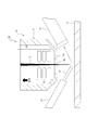
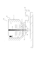
- FIG. 1-1 is a cross-sectional explanatory view of a main part of the focused ion beam apparatus according to the first embodiment of the present invention, and shows a state in which the surface of the substrate to be processed is observed.
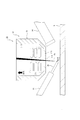
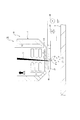
- FIG. 1-2 is a cross-sectional explanatory view of a main part of the focused ion beam device according to the first embodiment of the present invention, in which the charge-up on the surface of the substrate to be processed is neutralized with secondary electrons. show.
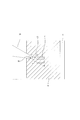
- FIG. 1-3 is a plan explanatory view showing a state in which an ion beam is scanned by the focused ion beam device according to the first embodiment of the present invention.
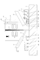
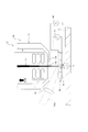
- FIG. 2 is a cross-sectional explanatory view of a main part of the focused ion beam device according to the second embodiment of the present invention.
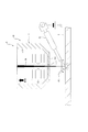
- FIG. 3-1 is a cross-sectional explanatory view of a main part of the focused ion beam apparatus according to the third embodiment of the present invention, and shows a state in which the surface of the substrate to be processed is observed.
- FIG. 3-2 is a cross-sectional explanatory view of a main part of the focused ion beam apparatus according to the third embodiment of the present invention, and shows a state in which the charge-up on the surface of the substrate to be processed is neutralized.
- FIG. 4 is a cross-sectional explanatory view of a main part of the focused ion beam device according to the fourth embodiment of the present invention.
- FIG. 3-1 is a cross-sectional explanatory view of a main part of the focused ion beam apparatus according to the third embodiment of the present invention, and shows a state in which the surface of the substrate to be processed is
- FIG. 5 is a cross-sectional explanatory view of a main part of the focused ion beam device according to the fifth embodiment of the present invention.
- FIG. 6 is a cross-sectional explanatory view of a main part of the focused ion beam device according to the sixth embodiment of the present invention.
- FIG. 1-1 shows a schematic configuration of the focused ion beam device 1A according to the first embodiment.
- the focused ion beam device 1A is a scintillator in which a substrate support that can move in the XY directions, a focused ion beam column (hereinafter referred to as a FIB column) 10, and a light guide are optically connected to the scintillator (not shown).
- a light guide 14 and a tungsten needle 20 as an electron supply unit are provided.
- the focused ion beam device 1A for example, observation of the surface state of a photomask having a Cr pattern formed on quartz glass, etching (sputtering) of a defective portion of the Cr pattern, and pattern correction are performed. It can be used for various pattern correction processes such as CVD film formation of a film.
- the FIB column 10 has a focused ion beam optical system 12 built in the lens barrel 11.
- a tip opening 11B is formed in the center of the tip (tip wall) 11A of the FIB column 10.
- the focused ion beam Ib is emitted toward the surface of the substrate S to be processed by passing the focused ion beam Ib through the tip opening 11B.
- the focused ion beam optical system 12 includes an ion source (not shown) that generates an ion beam, a condenser lens (not shown) that focuses the generated ion beam, a deflector (not shown) that scans the focused ion beam Ib, and a focused ion beam Ib.
- An objective electrostatic lens 13 for focusing is provided.
- a gallium (Ga) ion source is mainly used, but a rare gas ion source obtained by inductively coupled plasma (ICP) or gas electric field ionization of a rare gas such as argon (Ar) may be used. Is also possible.
- the focused ion beam Ib can be raster-scanned with the trajectory T as shown in FIG. 1-3, or the focused ion beam Ib can be set in an arbitrary direction. You can move it to.
- the scintillator / light guide 14 is provided integrally with the FIB column 10 in the vicinity of the tip portion 11A of the lens barrel 11.
- the scintillator / light guide 14 is arranged so as to face the substrate S to be processed in the region to be irradiated with the focused ion beam Ib emitted from the FIB column 10.
- the scintillator / write guide 14 receives secondary charged particles such as secondary electrons and backscattered electrons generated from the substrate S side to be processed and converts these electrons into light (about 10 kV from a high voltage power supply (not shown in this scintillator). Acceleration voltage is applied).
- a photomultiplier tube (photomultiplier: PMT) (not shown) is connected to the scintillator / light guide 14.
- a photomultiplier tube detects weak light emission from the scintillator / light guide 14 and outputs it as an electric signal. Based on the amount of this electric signal, it is possible to observe the state of the surface of the substrate S to be processed.
- the tungsten needle 20 is provided integrally with the FIB column 10 so as to protrude from the tip of the support portion 21.
- tungsten (W) is applied as the metal of the metal needle, but when the focused ion beam Ib is irradiated, secondary electrons are generated and other materials are used as long as they are metal materials that are difficult to be sputtered. May be applied.
- the tip of the tungsten needle 20 is located near the path of the focused ion beam Ib emitted from the FIB column 10 and close to the substrate S to be processed. It is set to be.
- a metal material having a high boiling point is preferable.
- a metal having a boiling point of 2000 ° C. or higher is preferable, and a metal having a boiling point of 5000 ° C. or higher is more preferable.
- Typical examples of metals include aluminum, copper, silver, gold, iron, chromium, tin, iridium, platinum, nickel, titanium, palladium, tungsten and the like.
- Tungsten has a high boiling point and is preferable. Further, it may be an alloy instead of a single metal.
- FIG. 1-1 shows a step of observing the surface state of the substrate S to be processed by using the focused ion beam device 1A.
- the substrate S to be processed is placed and set on a substrate support base (not shown) of the focused ion beam device 1A. Then, the substrate S to be processed is scanned in the XY directions so that a predetermined region of the substrate S to be processed faces the tip opening 11B of the FIB column 10.
- the surface of the substrate S to be processed is irradiated with the focused ion beam Ib.
- the focused ion beam Ib is raster-scanned so as to draw a locus T as shown in FIG. 1-3.
- the hatched region shown in FIG. 1-3 is, for example, a Cr mask pattern Sf.
- the area other than the hatch area is a glass surface in the case of a Cr mask.
- the focused ion beam device 1A is set to periodically change the course of the focused ion beam Ib to irradiate the tungsten needle 20 before the substrate S to be processed is charged up, as shown in FIG. 1-2. ing.
- the tungsten needle 20 when the tungsten needle 20 is irradiated with the focused ion beam Ib, secondary electrons are emitted from the tungsten needle 20. Since the tip of the tungsten needle 20 is set at a position close to the region irradiated with the focused ion beam Ib on the substrate S to be processed, the emitted secondary electrons neutralize the charge on the substrate S to be processed. To prevent charge-up.
- the tungsten needle 20 is connected to the ground / common ground of the apparatus. Therefore, in this focused ion beam device 1A, the position shift of the focused ion beam Ib and the insulation destruction of the sample can be prevented by the charge-up, and the observation by the focused ion beam Ib can be performed normally.
- the focused ion beam Ib is set to return to the planned observation position and continue the next raster scan.
- the focused ion beam device 1A was applied to the step of observing the surface of the substrate S to be processed, but the focused ion beam Ib was described as having a defective pattern of the substrate S to be processed.
- it can also be applied to the process of irradiating a spot (black defect) and sputtering the pattern to remove it.
- the charge can be neutralized before the substrate S to be processed is charged up. Therefore, etching (sputtering) of a defective portion of the pattern can be normally performed without displacement.
- the electron supply unit by the metal needle is CVD (chemical vapor deposition) by the focused ion beam Ib and the film forming gas. ) It can also be applied when forming a film.
- CVD film formation by the focused ion beam device 1A since the movement of the focused ion beam Ib is kept normal, good CVD film formation can be performed.
- the tungsten needle 20 which is a metal needle is applied as the electron supply unit, but a metal plate such as a tungsten plate may be used. Further, as the metal, as described above, a material other than tungsten may be applied as long as it is a metal material that generates secondary electrons when irradiated with the focused ion beam Ib and is difficult to be sputtered. Since the metal needle is a conductive material, it is preferable to connect it to the ground because the needle irradiated with the ion beam does not charge up.
- the charge-up can be efficiently prevented by a simple configuration in which the tungsten needle 20 is arranged in the vicinity of the path of the focused ion beam Ib. Therefore, according to the focused ion beam device 1A according to the present embodiment, cost reduction can be achieved.
- FIG. 2 shows a schematic configuration of a focused ion beam device 1B according to a second embodiment of the present invention.
- the differential exhaust device 30 is provided at the tip end portion 11A of the FIB column 10.
- a scintillator / light guide 14 and a support portion 21 provided with a tungsten needle 20 are provided in the vicinity of the tip portion 11A of the FIB column 10 in a state of penetrating the lens barrel 11.
- the focused ion beam device 1B according to the present embodiment is the same as the focused ion beam device 1A according to the first embodiment described above. Is set to face the substrate S to be processed in the area to be irradiated with.
- the tip of the tungsten needle 20 is set so as to be near the path of the focused ion beam Ib emitted from the FIB column 10 and at a position close to the substrate S to be processed.
- the differential exhaust device 30 includes a vacuum pump (not shown) and a head portion 31 shown in FIG.
- the head portion 31 is composed of a disk-shaped metal plate having a very small area compared to the area of the surface of the substrate S to be processed.
- the head portion 31 can face an arbitrary region of the substrate S to be processed by moving a substrate support (not shown) in the XY directions.
- a head opening 32 communicating with the tip opening 11B formed in the tip 11A of the lens barrel 11 is formed in the center of the head portion 31.
- the tip opening 11B and the head opening 32 are set to have substantially the same diameter.
- the head portion 31 has a flange-like structure provided at the end of the lens barrel 11.
- four annular grooves 33, 34A, 34B, 34C arranged concentrically with respect to the center of the head opening 32 are formed.
- At least one (three in the present embodiment) annular grooves 34A, 34B, 34C among these plurality of annular grooves 33, 34A, 34B, 34C are connected to a vacuum pump (not shown).
- the innermost annular groove 33 is connected to a depot gas supply source (not shown) that supplies depot gas (deposit gas, CVD gas).
- the head portion 31 faces the space inside the head opening 32 and the lens barrel by the air suction action from the annular grooves 34A, 34B, 34C in a state where the surface of the substrate S to be processed faces the lower surface via a predetermined gap. It has a function to make the space in 11 a high degree of vacuum.
- the lens barrel 11 is separately sucked by a vacuum pump (not shown).
- the head portion 31 reliably supplies the deposition gas from the innermost annular groove 33 to the surface of the substrate S to be processed so as to be adjusted to a high degree of vacuum, and to the region where the focused ion beam Ib is irradiated. It is possible to perform CVD film formation.
- the CVD gas for deposition for example, W (CO) 6 can be used.
- W (CO) 6 can be used as the CVD gas for deposition.
- the focused ions are applied to the tungsten needle 20 before the surface of the substrate S to be irradiated with the focused ion beam Ib is charged up.
- the beam Ib By irradiating the beam Ib, secondary electrons can be generated to neutralize the charge.
- the focused ion beam device 1B can etch (sputter) the surface of the substrate S to be processed by normal irradiation without irradiating the tungsten needle 20 with the focused ion beam Ib. Then, before the surface of the substrate S to be processed is charged with a positive charge and charged up, the tungsten needle 20 is irradiated with the focused ion beam Ib to neutralize the charge.
- FIG. 2 shows a process of observing the surface state of the substrate S to be processed using the focused ion beam device 1B.
- the differential exhaust device 30 is operated to set the space inside the lens barrel 11 and the space inside the head opening 32 to a high vacuum.
- the supply of the depot gas to the annular groove 33 is stopped.
- the configuration of the focused ion beam device 1B according to the present embodiment has been described above, but the configurations other than the differential exhaust device 30 are substantially the same as the focused ion beam device 1A according to the first embodiment described above. Therefore, the description is omitted.
- this focused ion beam device 1B since a large vacuum chamber is not required, cost reduction can be achieved with a compact and simple configuration, and charge-up can be efficiently prevented. As a result, according to the focused ion beam apparatus 1B according to the present embodiment, it is possible to accurately observe the surface of the substrate S to be processed, etching (sputtering) capable of reliable processing, and high-quality CVD film formation.
- FIG. 3-1 shows a schematic configuration of a focused ion beam device 2A according to a third embodiment of the present invention.
- the microchannel plate 40 is provided in the vicinity below the tip portion 11A of the lens barrel 11.
- an ion beam passage port 41 having a relatively large diameter is opened in the center, and the peripheral portion thereof is a secondary charge generated from the substrate S to be processed.
- a detection unit 42 capable of capturing particles is provided. That is, the microchannel plate 40 has a detection unit 42 outside the ion beam passage port 41.
- a voltage source 43 and an ammeter 44 are appropriately connected to the microchannel plate 40.
- the microchannel plate 40 is made of glass, which is a highly insulating material.
- the detection unit 42 is formed with a large number of thin tubes (microchannels) penetrating from one surface to the other.
- the focused ion beam Ib is irradiated with the supply of the depot gas stopped.
- the voltage source 43 applies a high voltage to the surface on which the focused ion beam Ib is incident.
- electrons are generated in the detection unit 42 by the incident of the secondary charged particles generated from the surface of the substrate S to be processed to which the focused ion beam Ib is incident. In this way, by amplifying the generated electrons with an avalanche current and measuring with an ammeter 44, it is possible to obtain information on the surface of the substrate S to be processed.
- FIG. 3-2 shows an operation when the focused ion beam device 2A is used to neutralize the charge of the substrate S to be processed.
- the focused ion beam Ib is changed in course by operating the focused ion beam optical system 12. Specifically, the focused ion beam Ib is changed in course so as to periodically irradiate the inner wall 41A of the ion beam passage port 41 of the microchannel plate 40. At this time, the voltage applied from the voltage source 43 to the microchannel plate 40 is set so as to have a reverse bias. Then, as shown in FIG.
- the focused ion beam Ib is converted into electrons in the inner wall 41A of the ion beam passage port 41 of the microchannel plate 40 and in the thin tube (microchannel), and is amplified several tens of times.
- the secondary electrons are supplied to the irradiated position of the focused ion beam Ib on the substrate S to be processed to prevent charge-up.
- the focused ion beam device 2A According to the focused ion beam device 2A according to the present embodiment, secondary electrons can be generated by using the microchannel plate 40 used for surface observation, so that cost reduction can be achieved with a simple configuration, and moreover, the cost can be reduced. Charge-up can be prevented efficiently. Therefore, according to the focused ion beam device 2A, there is an effect that the processing using the focused ion beam Ib can be normally performed.
- this focused ion beam device 2A there is an effect that various processing operations can be continuously performed without interruption. Therefore, according to the focused ion beam device 2A according to the present embodiment, workability can be improved.
- FIG. 4 shows a schematic configuration of a focused ion beam device 2B according to a fourth embodiment of the present invention.
- the configuration of the focused ion beam device 2B is such that the focused ion beam device 2A according to the third embodiment is provided with the differential exhaust device 30.
- the annular groove 33 supplies the depot gas, and the annular groove 34 exhausts the gas.
- the microchannel plate 40 is arranged below the objective electrostatic lens 13 in the lens barrel 11. Since the other configurations of the focused ion beam device 2B according to the present embodiment are substantially the same as those of the focused ion beam device 2A according to the third embodiment, the description thereof will be omitted.
- the operation and operation of the focused ion beam device 2B according to the present embodiment is substantially the same as that of the focused ion beam device 2A according to the third embodiment, and the charged substrate S is charged before being charged. Can be harmonized. According to this focused ion beam device 2B, there is an effect that various processing operations can be continuously performed without interruption. According to the focused ion beam device 2B according to the present embodiment, the workability can be improved because of the compact structure.
- the working distance (WD) of the objective electrostatic lens 13 can be brought close to each other.
- the working distance of the objective electrostatic lens 13 is shortened in this way, it becomes difficult to separately arrange a structure such as a depot gas nozzle near the tip of the lens barrel 11.
- the annular groove 33 for supplying the depot gas is also provided at the tip of the lens barrel 11, it is possible to irradiate the focused ion beam Ib while reliably supplying the depot gas to the substrate S to be processed. can. Therefore, according to the present embodiment, the problem that the supply of depot gas becomes difficult due to the shortening of the working distance does not occur.
- the working distance of the objective electrostatic lens 13 can be shortened, so that the focusing efficiency of the focused ion beam optical system 12 is also improved, and the fine focused ion beam Ib It is also possible to irradiate.
- the position of the substrate S to be processed for observing the surface state by the focused ion beam Ib and the position of the substrate S to be processed when performing the CVD film formation are the same, so that the substrate S to be processed is the same. There is no need to move. Therefore, it is possible to avoid the problem that the processing position shifts as the substrate S to be processed moves.
- FIG. 5 shows a schematic configuration of a focused ion beam device 3 according to a fifth embodiment of the present invention.
- the focused ion beam device 3 is configured to include a microchannel plate 40, similarly to the focused ion beam device 2A according to the third embodiment described above.
- the configuration different from the focused ion beam device 2A according to the third embodiment is to periodically send UV light to the microchannel plate 40 from a UV light irradiation means (not shown). Is irradiated to generate secondary electrons.
- the focused ion beam device 3 includes a lens 50 for directing UV light to the microchannel plate 40.
- the charge on the substrate S to be processed can be neutralized even during the processing with the focused ion beam Ib, so that the work efficiency can be improved without interrupting the work.
- UV light is transmitted to the microchannel plate 40.
- the approach angle of the UV light may be set shallow so that it can be guided.
- FIG. 6 shows a schematic configuration of the focused ion beam device 4 according to the sixth embodiment of the present invention.
- the focused ion beam device 4 includes a substrate support (not shown) that can move in the XY directions, a FIB column 10, and a ring-shaped filament 60 that surrounds the focused ion beam Ib.
- the filament 60 is made of tungsten and is connected to the thermionic generator 61.
- a bias power source is connected to the thermionic generator 61 as a heating power source so that an optimum potential gradient can be created with respect to the charge-up voltage.
- the other configurations of the focused ion beam device 4 according to the present embodiment are the same as those of the focused ion beam device 1A according to the first embodiment.
- the filament 60 that generates thermions is arranged directly below the tip portion 11A of the lens barrel 11. Therefore, in the focused ion beam device 4, the charge of the substrate S to be processed can be reliably neutralized by thermions generated from the filament 60.
- the filament 60 is arranged so as to surround the path of the focused ion beam Ib, charge-up can be reliably and efficiently prevented in the region irradiated with the focused ion beam Ib. According to the focused ion beam device 4 according to the present embodiment, cost reduction can be achieved.
- thermions can be supplied from the filament 60, it is not necessary to deviate the orbit of the focused ion beam Ib from the orbit where normal processing is performed, so that more efficient charge-up can be prevented.
- the tungsten needle 20 is arranged in the vicinity of the focused ion beam Ib, but a ring-shaped tungsten ring is arranged so as to surround the path of the focused ion beam Ib. It may be configured to be used. Then, when the position of the focused ion beam Ib is displaced due to the charge in the region irradiated with the focused ion beam Ib of the substrate S to be processed, the focused ion beam Ib irradiates the tungsten ring with secondary electrons.
- the automatically generated configuration is also the scope of the present invention.
- the focused ion beam devices 3 and 4 according to the fifth and sixth embodiments described above are provided with a differential exhaust device.
- the microchannel plate 40 may be housed inside the lens barrel 11.
- UV light can be introduced into the microchannel plate 40 by arranging an optical fiber that allows UV light to pass through the lens barrel 11.
Landscapes
- Chemical & Material Sciences (AREA)
- Analytical Chemistry (AREA)
- Physics & Mathematics (AREA)
- Engineering & Computer Science (AREA)
- Plasma & Fusion (AREA)
- Drying Of Semiconductors (AREA)
- Electron Sources, Ion Sources (AREA)
Abstract
鏡筒の中に集束イオンビーム光学系を内蔵して集束イオンビームを前記鏡筒の先端部から出射する集束イオンビームカラムを備える集束イオンビーム装置であって、前記集束イオンビーム光学系から出射される前記集束イオンビームの進路の近傍に、被処理基板の表面に電子を供給する、金属針、金属片などの電子供給部や、2次荷電粒子を捕捉する検出部を備えるマイクロチャネルプレートなどが配置され、このような簡易な構成とすることにより集束イオンビーム装置の低コスト化を達成でき、しかも効率的にチャージアップを防止できる集束イオンビーム装置を提供できる。
Description
本発明は、集束イオンビーム装置に関する。
集束イオンビーム装置は、真空中でイオンを発生させ、静電場で集光して集束イオンビームとしている。集束イオンビーム装置では、集束したイオンビームが照射された位置から発生する2次荷電粒子(2次電子、2次イオンなど)を捕捉して、その強度情報をもとにイオンビームをスキャンしながら画像としてデータを取得する。このデータに基づいて、ビーム照射位置での強度情報を表示すると、イオンビームが照射されていたサンプルの表面形状が確認できる。
一方で、集束イオンビーム装置では、イオンビーム電流を増加してサンプル表面をスパッタリングして加工することもできる。この現象を利用して、集束イオンビーム装置を、フォトマスクなどの修正装置として用いることもできる。フォトマスクのパターンは、クロム(Cr)で形成されている。このパターンの不良(黒欠陥)箇所に集束イオンビームを照射して、パターンをスパッタリングして除去できる。集束イオンビーム装置では、上述したサンプルの表面形状の確認およびエッチング(スパッタリング)の機能に加えて、集束イオンビームと成膜用ガスによりCVD(化学気相成長)を行う機能などがある。
しかしながら、集束イオンビームは単極性のガリウム正イオンでなるため、照射し続けるとサンプル表面に正電荷が蓄積される。サンプル自体が絶縁体である場合は、サンプル表面がチャージアップして、照射する集束イオンビームが振れたり照射できなくなったりするという問題があった。
サンプル表面のチャージアップを防止する従来技術としては、イオンビームが照射されるサンプル表面へ向けて電子ビームを出射する中和用電子銃を備える荷電ビーム処理装置が知られている(例えば、特許文献1参照)。上記の中和用電子銃は、真空排気される筒体の中に、電子源と、電子光学系と、を備える。この荷電ビーム処理装置では、電子源から電子ビームを引き出し、電子ビームを電子銃コントローラで制御し、先端部から電子ビームを出射する。そして、この中和用電子銃の先端部は、サンプル表面の近傍に配置され、電子ビームがサンプル表面に照射されるように設定されている。
上記の従来の技術においては、筒体の先端部をサンプル表面の近傍に配置するように、集束イオンビーム装置の側方からサンプル表面の近傍に亘る領域に中和用電子銃を設置する必要があるため、装置全体が複雑となるとともに大型化してコストが増大するという課題がある。
本発明は、上記の課題に鑑みてなされたものであって、簡易な構成で低コスト化を達成でき、しかも効率的にチャージアップを防止できる集束イオンビーム装置を提供することを目的とする。
上述した課題を解決し、目的を達成するために、本発明の態様は、鏡筒の中に集束イオンビーム光学系を内蔵して集束イオンビームを前記鏡筒の先端部から出射する集束イオンビームカラムを備える集束イオンビーム装置であって、前記集束イオンビーム光学系から出射される前記集束イオンビームの進路の近傍に、被処理基板の表面に電子を供給する電子供給部が配置されることが好ましい。
上記態様としては、前記電子供給部は、前記集束イオンビームが照射されることにより2次電子を発生させることが好ましい。
上記態様としては、前記電子供給部は、金属針または金属片であることが好ましい。
上記態様としては、前記電子供給部は、前記集束イオンビームを通過させて前記被処理基板へ入射させるイオンビーム通過口を有し、イオンビーム通過口の外側に、被処理基板から発生した2次荷電粒子を捕捉可能な検出部を、有するマイクロチャネルプレートであることが好ましい。
上記態様としては、前記集束イオンビーム光学系は、前記集束イオンビームを前記マイクロチャネルプレートのイオンビーム通過口を通過する進路と、前記集束イオンビームを前記マイクロチャネルプレートに照射する進路と、を選択可能であり、前記マイクロチャネルプレートは、前記集束イオンビームが照射されるときに逆バイアスが印加されるように設定されていることが好ましい。
上記態様としては、UV光照射手段を備え、前記電子供給部は、前記UV光照射手段からUV光が照射されることにより光電子を発生させることが好ましい。
上記態様としては、前記電子供給部は、前記集束イオンビームを通過させて前記被処理基板へ入射させるイオンビーム通過口を有し、前記イオンビーム通過口の外側に被処理基板から発生した2次荷電粒子を捕捉可能な検出部を有するマイクロチャネルプレートであることが好ましい。
上記態様としては、前記マイクロチャネルプレートは、前記UV光が照射されるときに逆バイアスが印加されるように設定されていることが好ましい。
上記態様としては、前記電子供給部は、前記集束イオンビーム光学系の先端側に配置された、熱電子を発生するフィラメントであることが好ましい。
上記態様としては、集束イオンビームカラムの先端部に、差動排気装置を備えることが好ましい。
本発明によれば、簡易な構成で低コスト化を達成でき、しかも効率的にチャージアップを防止できる集束イオンビーム装置を実現できる。
以下、本発明の実施の形態に係る集束イオンビーム装置の詳細を図面に基づいて説明する。なお、図面は模式的なものであり、各部材の寸法や寸法の比率や数、形状などは現実のものと異なることに留意すべきである。また、図面相互間においても互いの寸法の関係や比率や形状が異なる部分が含まれている。
[第1の実施の形態](集束イオンビーム装置の概略構成)
図1-1は、第1の実施の形態に係る集束イオンビーム装置1Aの概略構成を示している。集束イオンビーム装置1Aは、図示しない、X-Y方向に移動可能な基板支持台と、集束イオンビームカラム(以下、FIBカラムという)10と、シンチレータにライトガイドを光学的に接続してなるシンチレータ・ライトガイド14と、電子供給部としてのタングステン針20と、を備える。本実施の形態に係る集束イオンビーム装置1Aは、例えば、石英ガラスの上に形成されたCrパターンを有するフォトマスクの表面状態の観察や、Crパターンの欠陥箇所のエッチング(スパッタリング)や、パターン修正膜のCVD成膜などの、各種のパターン修正を目的とする処理に用いることができる。
図1-1は、第1の実施の形態に係る集束イオンビーム装置1Aの概略構成を示している。集束イオンビーム装置1Aは、図示しない、X-Y方向に移動可能な基板支持台と、集束イオンビームカラム(以下、FIBカラムという)10と、シンチレータにライトガイドを光学的に接続してなるシンチレータ・ライトガイド14と、電子供給部としてのタングステン針20と、を備える。本実施の形態に係る集束イオンビーム装置1Aは、例えば、石英ガラスの上に形成されたCrパターンを有するフォトマスクの表面状態の観察や、Crパターンの欠陥箇所のエッチング(スパッタリング)や、パターン修正膜のCVD成膜などの、各種のパターン修正を目的とする処理に用いることができる。
(FIBカラム)
FIBカラム10は、鏡筒11内に集束イオンビーム光学系12が内蔵されている。FIBカラム10の先端部(先端壁部)11Aの中央には、先端開口部11Bが形成されている。FIBカラム10では、集束イオンビームIbを、先端開口部11Bを通過させることにより、被処理基板Sの表面に向けて出射するようになっている。
FIBカラム10は、鏡筒11内に集束イオンビーム光学系12が内蔵されている。FIBカラム10の先端部(先端壁部)11Aの中央には、先端開口部11Bが形成されている。FIBカラム10では、集束イオンビームIbを、先端開口部11Bを通過させることにより、被処理基板Sの表面に向けて出射するようになっている。
(集束イオンビーム光学系)
集束イオンビーム光学系12は、イオンビームを発生させる図示しないイオン源と、発生したイオンビームを集束させる図示しないコンデンサレンズと、集束イオンビームIbを走査する図示しない偏向器と、集束イオンビームIbを集束させる対物静電レンズ13と、を備える。イオン源としては、主にガリウム(Ga)イオン源を用いるが、アルゴン(Ar)など希ガスを誘導結合プラズマ(ICP)化したり、ガス電界イオン化したりした、希ガスイオン源を用いたりすることも可能である。集束イオンビームIbのレンズとしては、電界レンズを用いることが好ましい。本実施の形態では、偏向器や対物静電レンズ13などを調整することにより、図1-3に示すような軌跡Tで集束イオンビームIbをラスタスキャンしたり、集束イオンビームIbを任意の方向へ移動させたりできる。
集束イオンビーム光学系12は、イオンビームを発生させる図示しないイオン源と、発生したイオンビームを集束させる図示しないコンデンサレンズと、集束イオンビームIbを走査する図示しない偏向器と、集束イオンビームIbを集束させる対物静電レンズ13と、を備える。イオン源としては、主にガリウム(Ga)イオン源を用いるが、アルゴン(Ar)など希ガスを誘導結合プラズマ(ICP)化したり、ガス電界イオン化したりした、希ガスイオン源を用いたりすることも可能である。集束イオンビームIbのレンズとしては、電界レンズを用いることが好ましい。本実施の形態では、偏向器や対物静電レンズ13などを調整することにより、図1-3に示すような軌跡Tで集束イオンビームIbをラスタスキャンしたり、集束イオンビームIbを任意の方向へ移動させたりできる。
(シンチレータ・ライトガイド)
図1-1および図1-2に示すように、シンチレータ・ライトガイド14は、鏡筒11の先端部11Aの近傍にFIBカラム10と一体的に設けられている。シンチレータ・ライトガイド14は、FIBカラム10から出射された集束イオンビームIbが照射される領域の被処理基板Sに対向するように配置されている。シンチレータ・ライトガイド14は、被処理基板S側から発生した2次電子や反射電子などの2次荷電粒子を受けてこれら電子を光に変換する(このシンチレータには図示しない高電圧電源から10kV程度の加速電圧が印加されている)。また、このシンチレータ・ライトガイド14には、図示しない光電子倍増管(フォトマル:PMT)が接続されている。図示しない光電子倍増管は、シンチレータ・ライトガイド14での微弱な発光を検出して電気信号として出力する。この電気信号の量に基づいて、被処理基板Sの表面の状態を観察することが可能である。
図1-1および図1-2に示すように、シンチレータ・ライトガイド14は、鏡筒11の先端部11Aの近傍にFIBカラム10と一体的に設けられている。シンチレータ・ライトガイド14は、FIBカラム10から出射された集束イオンビームIbが照射される領域の被処理基板Sに対向するように配置されている。シンチレータ・ライトガイド14は、被処理基板S側から発生した2次電子や反射電子などの2次荷電粒子を受けてこれら電子を光に変換する(このシンチレータには図示しない高電圧電源から10kV程度の加速電圧が印加されている)。また、このシンチレータ・ライトガイド14には、図示しない光電子倍増管(フォトマル:PMT)が接続されている。図示しない光電子倍増管は、シンチレータ・ライトガイド14での微弱な発光を検出して電気信号として出力する。この電気信号の量に基づいて、被処理基板Sの表面の状態を観察することが可能である。
(タングステン針:金属針)
タングステン針20は、支持部21の先端部に突出するように、FIBカラム10と一体的に設けられている。本実施の形態では、金属針の金属としてタングステン(W)を適用したが、集束イオンビームIbが照射されたときに、2次電子を発生させるとともに、スパッタリングされにくい金属材料であれば他の材料を適用してもよい。図1-1および図1-2に示すように、タングステン針20の先端部は、FIBカラム10から出射される集束イオンビームIbの進路の近傍で、しかも被処理基板Sに対して近接した位置になるように設定されている。
タングステン針20は、支持部21の先端部に突出するように、FIBカラム10と一体的に設けられている。本実施の形態では、金属針の金属としてタングステン(W)を適用したが、集束イオンビームIbが照射されたときに、2次電子を発生させるとともに、スパッタリングされにくい金属材料であれば他の材料を適用してもよい。図1-1および図1-2に示すように、タングステン針20の先端部は、FIBカラム10から出射される集束イオンビームIbの進路の近傍で、しかも被処理基板Sに対して近接した位置になるように設定されている。
スパッタリングされにくい金属材料としては、沸点が高いものが好ましい。沸点が2000℃以上の金属が好ましく、沸点が5000℃以上の金属がより好ましい。金属の代表例としては、アルミニウム、銅、銀、金、鉄、クロム、スズ、イリジウム、白金、ニッケル、チタン、パラジウム、タングステンなどが挙げられる。タングステンは沸点が高く好ましい。また、単体の金属ではなく、合金であっても良い。
(集束イオンビーム装置の作用・動作)
図1-1は、集束イオンビーム装置1Aを用いて被処理基板Sの表面状態を観察する工程を示している。
図1-1は、集束イオンビーム装置1Aを用いて被処理基板Sの表面状態を観察する工程を示している。
まず、集束イオンビーム装置1Aの図示しない基板支持台上に被処理基板Sを載せてセットする。そして、被処理基板SをX-Y方向に走査して、被処理基板Sの所定の領域がFIBカラム10の先端開口部11Bと対向するように配置させる。
図1-1に示すように、集束イオンビームIbを被処理基板Sの表面に照射する。このとき、集束イオンビーム装置1Aでは、集束イオンビームIbを、図1-3に示すような軌跡Tを描くようにラスタスキャンさせる。なお、図1-3に示すハッチング領域は、例えば、CrマスクパターンSfである。なお、ハッチングエリア以外はCrマスクの場合はガラス面である。
このように、集束イオンビームIbを被処理基板Sに照射することにより、Ga+イオンの衝突により被処理基板Sからは2次荷電粒子が放出される。被処理基板Sから放出された2次荷電粒子は、シンチレータ・ライトガイド14に入射して2次荷電粒子の量に応じた光に変換される。図示しない光電子倍増管は、シンチレータ・ライトガイド14での微弱な発光を検出して電気信号として出力する。この電気信号の量に基づいて、被処理基板Sの表面の状態を観察することが可能である。
このような集束イオンビームIbの照射を行うと、時間の経過とともにGa+イオンの衝突により被処理基板Sに正電荷が蓄積されて帯電する。集束イオンビーム装置1Aでは、被処理基板Sがチャージアップする前に、図1-2に示すように、定期的に集束イオンビームIbの進路を変更してタングステン針20に照射するように設定されている。
図1-2に示すように、タングステン針20に集束イオンビームIbが照射されると、タングステン針20から2次電子が放出される。タングステン針20の先端部は、被処理基板Sにおける集束イオンビームIbが照射された領域に近接した位置に設定されているため、放出された2次電子は被処理基板Sの帯電を中和してチャージアップを防止する。
なお、タングステン針20は装置のアース・コモングランドに接続されている。このため、この集束イオンビーム装置1Aでは、チャージアップにより、集束イオンビームIbの位置ずれやサンプルの絶縁破壊を防止でき、集束イオンビームIbによる観察を正常に行える。
なお、タングステン針20は装置のアース・コモングランドに接続されている。このため、この集束イオンビーム装置1Aでは、チャージアップにより、集束イオンビームIbの位置ずれやサンプルの絶縁破壊を防止でき、集束イオンビームIbによる観察を正常に行える。
図1-3に示すように、集束イオンビームIbをタングステン針20に照射した後は、集束イオンビームIbを観察予定位置に戻して次のラスタスキャンを続けるように設定されている。
なお、図1-3に示すように、被処理基板Sの表面を観察する工程にこの集束イオンビーム装置1Aを適用して説明したが、集束イオンビームIbを被処理基板Sのパターンの不良(黒欠陥)箇所に照射して、パターンをスパッタリングして除去する工程にも勿論適用できる。この場合においても、集束イオンビームIbの照射により被処理基板Sが局所的に帯電しても、被処理基板Sがチャージアップする前に、帯電を中和することができる。このため、パターンの不良箇所のエッチング(スパッタリング)を位置ずれなく、正常に行うことができる。
この集束イオンビーム装置1Aでは、金属針による電子供給部を、上述した被処理基板Sの表面観察およびエッチング(スパッタリング)に加えて、集束イオンビームIbと成膜用ガスによりCVD(化学気相成長)成膜を行う場合にも適用できる。集束イオンビーム装置1AによるCVD成膜においては、集束イオンビームIbの動きを正常に保てるため、良好なCVD成膜が行える。
なお、本実施の形態では、電子供給部として金属針であるタングステン針20を適用したが、タングステン板などの金属板であってもよい。また、金属としては、上述したように、集束イオンビームIbが照射されたときに、2次電子を発生させるとともに、スパッタリングされにくい金属材料であればタングステン以外の材料を適用してもよい。なお、金属針は、導電性材料のため、アースに接続しておくと、イオンビームが照射された針がチャージアップせず、好ましい。
上述したように、本実施の形態では、タングステン針20を集束イオンビームIbの進路の近傍に配置するという簡易な構成で、チャージアップを効率的に防止できる。このため、本実施の形態に係る集束イオンビーム装置1Aによれば、低コスト化を達成できる。
[第2の実施の形態](集束イオンビーム装置の概略構成)
図2は、本発明の第2の実施の形態に係る集束イオンビーム装置1Bの概略構成を示している。本実施の形態の集束イオンビーム装置1Bは、FIBカラム10の先端部11Aに、差動排気装置30が設けられている。FIBカラム10の先端部11Aの近傍には、鏡筒11に対して、シンチレータ・ライトガイド14と、タングステン針20を備えた支持部21と、が貫通した状態で設けられている。
図2は、本発明の第2の実施の形態に係る集束イオンビーム装置1Bの概略構成を示している。本実施の形態の集束イオンビーム装置1Bは、FIBカラム10の先端部11Aに、差動排気装置30が設けられている。FIBカラム10の先端部11Aの近傍には、鏡筒11に対して、シンチレータ・ライトガイド14と、タングステン針20を備えた支持部21と、が貫通した状態で設けられている。
本実施の形態に係る集束イオンビーム装置1Bは、上記した第1の実施の形態に係る集束イオンビーム装置1Aと同様に、シンチレータ・ライトガイド14は、FIBカラム10から出射された集束イオンビームIbが照射される領域の被処理基板Sに対向するように設定されている。
また、タングステン針20の先端部は、FIBカラム10から出射される集束イオンビームIbの進路の近傍で、しかも被処理基板Sに対して近接した位置になるように設定されている。
差動排気装置30は、ともに図示しない真空ポンプと、図2に示すヘッド部31と、を備える。
ヘッド部31は、被処理基板Sの表面の面積に比較してごく小さな面積の円盤形状の金属プレートによって構成されている。ヘッド部31は、図示しない基板支持台がX-Y方向に移動することにより、被処理基板Sの任意領域に対向し得るようになっている。
図2に示すように、ヘッド部31の中央には、鏡筒11の先端部11Aに形成された先端開口部11Bと連通するヘッド開口部32が形成されている。これら先端開口部11Bとヘッド開口部32は、略同じ径寸法に設定されている。ヘッド部31は、鏡筒11の端部に設けられたフランジ状の構造をなしている。ヘッド部31の下面には、ヘッド開口部32の中心を基準として、同心円状に配置された4つの環状溝33,34A,34B,34Cが形成されている。
これら複数の環状溝33,34A,34B,34Cのうち少なくとも1つ以上(本実施の形態では3つ)の環状溝34A,34B,34Cは、図示しない真空ポンプに接続されている。最も内側の環状溝33は、デポガス(堆積用ガス、CVD用ガス)を供給する図示しないデポガス供給源に接続されている。
ヘッド部31は、被処理基板Sの表面と所定のギャップを介して下面を対向させた状態で、環状溝34A,34B,34Cからの空気吸引作用により、ヘッド開口部32内の空間および鏡筒11内の空間を高真空度にする機能を備える。なお、鏡筒11は、別途、図示しない真空ポンプで空気吸引されるようになっている。
ヘッド部31は、このように高真空度に調整された被処理基板Sの表面へ、最も内側の環状溝33から堆積用ガスを確実に供給して、集束イオンビームIbが照射される領域へCVD成膜を行うことを可能にしている。CVDのデポジション用ガスとしては、例えば、W(CO)6を用いることができる。基板近傍のW(CO)6に集束イオンビームIbが照射されると、WとCOに分解され、Wが基板上にデポジションされる。このように、集束イオンビーム装置1Bを用いて、CVD成膜を行う場合に、集束イオンビームIbが照射される被処理基板Sの表面にチャージアップが発生する前に、タングステン針20に集束イオンビームIbを照射することで、2次電子を発生させて帯電を中和することができる。
集束イオンビーム装置1Bは、タングステン針20に集束イオンビームIbを照射させない通常の照射により、被処理基板Sの表面のエッチング(スパッタリング)を行うことができる。そして、被処理基板Sの表面に正電荷が帯電してチャージアップする前に、タングステン針20へ集束イオンビームIbを照射することにより、帯電を中和するようになっている。
図2は、集束イオンビーム装置1Bを用いて被処理基板Sの表面状態を観察する工程を示している。この場合、差動排気装置30を稼働させて、鏡筒11内部とヘッド開口部32内の空間を高真空に設定している。なお、このような観察を行う工程では、環状溝33へのデポガスの供給は停止させておく。
以上、本実施の形態に係る集束イオンビーム装置1Bの構成について説明したが、差動排気装置30以外の構成は、上記した第1の実施の形態に係る集束イオンビーム装置1Aと略同様であるため、説明を省略する。
この集束イオンビーム装置1Bによれば、大きな真空チャンバを必要としないため、コンパクトかつ簡易な構成で低コスト化を達成でき、しかも効率的にチャージアップを防止できる。この結果、本実施の形態に係る集束イオンビーム装置1Bによれば、被処理基板Sの表面の正確な観察、確実な加工が行えるエッチング(スパッタリング)、および良質なCVD成膜が可能となる。
[第3の実施の形態]
図3-1は、本発明の第3の実施の形態に係る集束イオンビーム装置2Aの概略構成を示している。特に、本実施の形態では、鏡筒11の先端部11Aの下方近傍にマイクロチャネルプレート40を備えている。
図3-1は、本発明の第3の実施の形態に係る集束イオンビーム装置2Aの概略構成を示している。特に、本実施の形態では、鏡筒11の先端部11Aの下方近傍にマイクロチャネルプレート40を備えている。
マイクロチャネルプレート40には、図3-1に示すように、中央に比較的径寸法の大きいイオンビーム通過口41が開けられており、その周辺部は、被処理基板Sから発生した2次荷電粒子を捕捉可能な検出部42が設けられている。すなわち、マイクロチャネルプレート40は、イオンビーム通過口41の外側に検出部42を有する。マイクロチャネルプレート40には、電圧源43や電流計44が適宜接続されている。マイクロチャネルプレート40は、高い絶縁性の材料であるガラスで形成されている。検出部42は、多数の細い管(マイクロチャネル)が一方の面から他方の面へ貫通して形成されている。
図3-1に示すように、集束イオンビーム装置2Aを用いて被処理基板Sの表面を観察する場合は、デポガスの供給を停止させた状態で集束イオンビームIbを照射する。このとき、電圧源43は、集束イオンビームIbが入射する面に高電圧を印加する。そして、集束イオンビームIbが入射した被処理基板Sの表面から発生した2次荷電粒子が入射することにより検出部42で電子が生じる。このように、生じた電子をアバランシェ電流により増幅して電流計44で測定することにより、被処理基板Sの表面の情報を得ることが可能となる。
図3-2は、この集束イオンビーム装置2Aを用いて、被処理基板Sの帯電を中和する場合の動作を示している。集束イオンビームIbを、集束イオンビーム光学系12を操作することにより進路変更させる。具体的には、集束イオンビームIbがマイクロチャネルプレート40のイオンビーム通過口41の内壁41Aを周期的に照射するように進路変更させる。このとき、電圧源43からマイクロチャネルプレート40に印加する電圧は、逆バイアスとなるように設定しておく。すると、図3-2に示すように、集束イオンビームIbがマイクロチャネルプレート40のイオンビーム通過口41の内壁41Aや細い管(マイクロチャネル)内で電子に変換され、かつ数十倍に増幅させた2次電子を、被処理基板Sにおける集束イオンビームIbを照射した位置へ供給することでチャージアップを防止する。
本実施の形態に係る集束イオンビーム装置2Aによれば、表面観察に用いるマイクロチャネルプレート40を利用して2次電子を発生させることができるため、簡易な構成で低コスト化を達成し、しかも効率的にチャージアップを防止できる。このため、集束イオンビーム装置2Aによれば、集束イオンビームIbを用いた処理が正常に行えるという効果がある。
また、この集束イオンビーム装置2Aによれば、各種の処理作業を中断することなく、継続して行えるという効果がある。このため、本実施の形態に係る集束イオンビーム装置2Aによれば、作業性を向上できる。
[第4の実施の形態]
図4は、本発明の第4の実施の形態に係る集束イオンビーム装置2Bの概略構成を示している。この集束イオンビーム装置2Bの構成は、上記第3の実施の形態に係る集束イオンビーム装置2Aに差動排気装置30を備える構成である。
図4は、本発明の第4の実施の形態に係る集束イオンビーム装置2Bの概略構成を示している。この集束イオンビーム装置2Bの構成は、上記第3の実施の形態に係る集束イオンビーム装置2Aに差動排気装置30を備える構成である。
集束イオンビーム装置2Bでは、環状溝33がデポガスを供給し、環状溝34が排気を行う。また、本実施の形態では、マイクロチャネルプレート40が鏡筒11内で対物静電レンズ13の下方に配置されている。本実施の形態に係る集束イオンビーム装置2Bにおけるその他の構成は、上記第3の実施の形態に係る集束イオンビーム装置2Aと略同様であるため、説明を省略する。
本実施の形態に係る集束イオンビーム装置2Bの作用・動作は、上記第3の実施の形態に係る集束イオンビーム装置2Aと略同様であり、被処理基板Sがチャージアップする前に帯電を中和することができる。この集束イオンビーム装置2Bによれば、各種の処理作業を中断することなく、継続して行えるという効果がある。本実施の形態に係る集束イオンビーム装置2Bによれば、コンパクトな構造であるため、作業性を向上できる。
図4に示すように、本実施の形態に係る集束イオンビーム装置2Bによれば、対物静電レンズ13のワーキングディスタンス(WD)を接近させることが可能となる。一般的に、このように対物静電レンズ13のワーキングディスタンスを短くすると鏡筒11の先端部近傍にデポガスのノズルなどの構造物を別途配置しにくくなる。しかし、本実施の形態では、デポガスを供給する環状溝33も鏡筒11の先端部に設けられているため、被処理基板Sへデポガスを確実に供給しつつ集束イオンビームIbを照射することができる。したがって、本実施の形態によれば、ワーキングディスタンスが短くなることに起因してデポガスの供給がしにくくなるという問題は発生しない。
上述のように、本実施の形態によれば、結果的には、対物静電レンズ13のワーキングディスタンスを短くできるので、集束イオンビーム光学系12の集束効率も向上し、微細な集束イオンビームIbを照射することも可能となる。また、本実施の形態では、集束イオンビームIbによる表面状態の観察を行う被処理基板Sの位置と、CVD成膜を行うときの被処理基板Sの位置は同じであるため、被処理基板Sを移動させる必要がない。このため、被処理基板Sの移動に伴って処理位置がずれるという問題を回避できる。
[第5の実施の形態]
図5は、本発明の第5の実施の形態に係る集束イオンビーム装置3の概略構成を示している。この集束イオンビーム装置3は、上記した第3の実施の形態に係る集束イオンビーム装置2Aと同様に、マイクロチャネルプレート40を備える構成である。本実施の形態に係る集束イオンビーム装置3おいて、第3の実施の形態に係る集束イオンビーム装置2Aと異なる構成は、マイクロチャネルプレート40に、図示しないUV光照射手段からUV光を定期的に照射して、2次電子を発生させるという点である。集束イオンビーム装置3は、UV光をマイクロチャネルプレート40へ導くために、レンズ50を備えている。
図5は、本発明の第5の実施の形態に係る集束イオンビーム装置3の概略構成を示している。この集束イオンビーム装置3は、上記した第3の実施の形態に係る集束イオンビーム装置2Aと同様に、マイクロチャネルプレート40を備える構成である。本実施の形態に係る集束イオンビーム装置3おいて、第3の実施の形態に係る集束イオンビーム装置2Aと異なる構成は、マイクロチャネルプレート40に、図示しないUV光照射手段からUV光を定期的に照射して、2次電子を発生させるという点である。集束イオンビーム装置3は、UV光をマイクロチャネルプレート40へ導くために、レンズ50を備えている。
本実施の形態では、UV光により2次電子を発生させるため、集束イオンビームIbの軌道を通常の処理を行う軌道から逸脱させる必要がないため、より効率的なチャージアップの防止が行える。すなわち、集束イオンビーム装置3によれば、集束イオンビームIbでの処理中でも、被処理基板Sの帯電を中和することができるため、作業を中断することなく作業効率を向上できる。
なお、この集束イオンビーム装置3においては、UV光を反射するミラーを配置して被処理基板Sと鏡筒11の先端部11Aとの距離を短くした場合でも、UV光をマイクロチャネルプレート40へ導けるようにUV光の進入角度を浅く設定してもよい。
[第6の実施の形態]
図6は、本発明の第6の実施の形態に係る集束イオンビーム装置4の概略構成を示している。集束イオンビーム装置4は、図示しない、X-Y方向に移動可能な基板支持台と、FIBカラム10と、集束イオンビームIbを取り囲むリング状のフィラメント60と、を備える。フィラメント60は、タングステンで形成され、熱電子発生装置61に接続されている。なお、熱電子発生装置61には、加熱電源としてバイアス電源が接続されていて、チャージアップ電圧に対して最適な電位勾配を作ることができるようになっている。
図6は、本発明の第6の実施の形態に係る集束イオンビーム装置4の概略構成を示している。集束イオンビーム装置4は、図示しない、X-Y方向に移動可能な基板支持台と、FIBカラム10と、集束イオンビームIbを取り囲むリング状のフィラメント60と、を備える。フィラメント60は、タングステンで形成され、熱電子発生装置61に接続されている。なお、熱電子発生装置61には、加熱電源としてバイアス電源が接続されていて、チャージアップ電圧に対して最適な電位勾配を作ることができるようになっている。
なお、本実施の形態に係る集束イオンビーム装置4におけるその他の構成は、第1の実施の形態に係る集束イオンビーム装置1Aと同様である。
本実施の形態においては、鏡筒11の先端部11Aの直下に、熱電子を発生させるフィラメント60を配置している。このため、集束イオンビーム装置4では、被処理基板Sの帯電をフィラメント60から発生する熱電子で確実に中和できる。この実施の形態では、フィラメント60を集束イオンビームIbの進路を取り囲むように配置するため、集束イオンビームIbが照射される領域において確実かつ効率的にチャージアップの防止ができる。本実施の形態に係る集束イオンビーム装置4によれば、低コスト化を達成できる。
本実施の形態では、フィラメント60から熱電子を供給できるため、集束イオンビームIbの軌道を通常の処理を行う軌道から逸脱させる必要がないため、より効率的なチャージアップの防止が行える。
[その他の実施の形態]
以上、本発明の実施の形態について説明したが、この実施の形態の開示の一部をなす論述および図面はこの発明を限定するものであると理解すべきではない。この開示から当業者には様々な代替実施の形態、実施例および運用技術が明らかとなろう。
以上、本発明の実施の形態について説明したが、この実施の形態の開示の一部をなす論述および図面はこの発明を限定するものであると理解すべきではない。この開示から当業者には様々な代替実施の形態、実施例および運用技術が明らかとなろう。
なお、本実施の形態では、集束イオンビーム装置1A,1B,2A,2B,3,4をフォトマスクの修正を目的として用いる例について説明したが、これに限定されるものではない。
上記した第1の実施の形態に係る集束イオンビーム装置1Aにおいては、タングステン針20を集束イオンビームIbの近傍に配置したが、集束イオンビームIbの進路を取り囲むようにリング状のタングステン環を配置する構成としてもよい。そして、被処理基板Sの集束イオンビームIbが照射される領域が帯電したことにより、集束イオンビームIbの位置がずれた際に、集束イオンビームIbがタングステン環に照射して、2次電子を自動的に発生させる構成も、本発明の適用範囲である。
上記の第5および第6の実施の形態に係る集束イオンビーム装置3,4に、差動排気装置を備える構成とすることも、本発明の適用範囲である。
上記の第5の実施の形態に係る集束イオンビーム装置3において、マイクロチャネルプレート40を鏡筒11の内部に収納してもよい。この場合、UV光を通す光ファイバーを、鏡筒11に対して貫通させて配置することにより、マイクロチャネルプレート40にUV光を導入できる。
Ib 集束イオンビーム
S 被処理基板
Sf Crマスクパターン
1A,1B,2A,2B,3,4 集束イオンビーム装置
10 集束イオンビームカラム(FIBカラム)
11 鏡筒
11A 先端部
11B 先端開口部
12 集束イオンビーム光学系
13 対物静電レンズ
14 シンチレータ・ライトガイド
20 タングステン針(電子供給部)
21 支持部
30 差動排気装置
31 ヘッド部
32 ヘッド開口部
33,34A,34B,34C 環状溝
40 マイクロチャネルプレート
41 イオンビーム通過口
41A 内壁
42 検出部
43 電圧源
44 電流計
50 レンズ
60 フィラメント
61 熱電子発生装置
S 被処理基板
Sf Crマスクパターン
1A,1B,2A,2B,3,4 集束イオンビーム装置
10 集束イオンビームカラム(FIBカラム)
11 鏡筒
11A 先端部
11B 先端開口部
12 集束イオンビーム光学系
13 対物静電レンズ
14 シンチレータ・ライトガイド
20 タングステン針(電子供給部)
21 支持部
30 差動排気装置
31 ヘッド部
32 ヘッド開口部
33,34A,34B,34C 環状溝
40 マイクロチャネルプレート
41 イオンビーム通過口
41A 内壁
42 検出部
43 電圧源
44 電流計
50 レンズ
60 フィラメント
61 熱電子発生装置
Claims (10)
- 鏡筒の中に集束イオンビーム光学系を内蔵して集束イオンビームを前記鏡筒の先端部から出射する集束イオンビームカラムを備える集束イオンビーム装置であって、
前記集束イオンビーム光学系から出射される前記集束イオンビームの進路の近傍に、被処理基板の表面に電子を供給する電子供給部が配置される、
集束イオンビーム装置。 - 前記電子供給部は、前記集束イオンビームが照射されることにより2次電子を発生させる、
請求項1に記載の集束イオンビーム装置。 - 前記電子供給部は、金属針または金属片である、
請求項2に記載の集束イオンビーム装置。 - 前記電子供給部は、前記集束イオンビームを通過させて前記被処理基板へ入射させるイオンビーム通過口を有し、イオンビーム通過口の外側に、前記被処理基板から発生した2次荷電粒子を捕捉可能な検出部を、有するマイクロチャネルプレートである、
請求項2に記載の集束イオンビーム装置。 - 前記集束イオンビーム光学系は、前記集束イオンビームを前記マイクロチャネルプレートのイオンビーム通過口を通過する進路と、前記集束イオンビームを前記マイクロチャネルプレートに照射する進路と、を選択可能であり、
前記マイクロチャネルプレートは、前記集束イオンビームが照射されるときに逆バイアスが印加されるように設定されている、
請求項4に記載の集束イオンビーム装置。 - UV光照射手段を備え、
前記電子供給部は、前記UV光照射手段からUV光が照射されることにより光電子を発生させる、
請求項1に記載の集束イオンビーム装置。 - 前記電子供給部は、前記集束イオンビームを通過させて前記被処理基板へ入射させるイオンビーム通過口を有し、前記イオンビーム通過口の外側に前記被処理基板から発生した2次荷電粒子を捕捉可能な検出部を有するマイクロチャネルプレートである、
請求項6に記載の集束イオンビーム装置。 - 前記マイクロチャネルプレートは、前記UV光が照射されるときに逆バイアスが印加されるように設定されている、
請求項7に記載の集束イオンビーム装置。 - 前記電子供給部は、前記集束イオンビーム光学系の先端側に配置された、熱電子を発生するフィラメントである、
請求項1に記載の集束イオンビーム装置。 - 集束イオンビームカラムの先端部に、差動排気装置を備える、
請求項1から請求項9のいずれか一項に記載の集束イオンビーム装置。
Priority Applications (2)
| Application Number | Priority Date | Filing Date | Title |
|---|---|---|---|
| KR1020237000382A KR20230034290A (ko) | 2020-07-02 | 2021-06-17 | 집속 이온빔 장치 |
| CN202180036774.8A CN115668433A (zh) | 2020-07-02 | 2021-06-17 | 聚焦离子束装置 |
Applications Claiming Priority (2)
| Application Number | Priority Date | Filing Date | Title |
|---|---|---|---|
| JP2020-115113 | 2020-07-02 | ||
| JP2020115113A JP2022012937A (ja) | 2020-07-02 | 2020-07-02 | 集束イオンビーム装置 |
Publications (1)
| Publication Number | Publication Date |
|---|---|
| WO2022004401A1 true WO2022004401A1 (ja) | 2022-01-06 |
Family
ID=79316040
Family Applications (1)
| Application Number | Title | Priority Date | Filing Date |
|---|---|---|---|
| PCT/JP2021/022972 Ceased WO2022004401A1 (ja) | 2020-07-02 | 2021-06-17 | 集束イオンビーム装置 |
Country Status (5)
| Country | Link |
|---|---|
| JP (1) | JP2022012937A (ja) |
| KR (1) | KR20230034290A (ja) |
| CN (1) | CN115668433A (ja) |
| TW (1) | TW202211288A (ja) |
| WO (1) | WO2022004401A1 (ja) |
Citations (4)
| Publication number | Priority date | Publication date | Assignee | Title |
|---|---|---|---|---|
| JPH08138617A (ja) * | 1994-11-10 | 1996-05-31 | Hitachi Ltd | 荷電ビーム処理装置およびその方法 |
| JPH09274883A (ja) * | 1996-04-03 | 1997-10-21 | Hitachi Ltd | Fib/sem複合装置 |
| JPH10269981A (ja) * | 1997-03-27 | 1998-10-09 | Ricoh Co Ltd | 電子/イオンビーム照射装置,該電子/イオンビーム照射装置を備える走査型電子顕微鏡,及び該電子/イオンビーム照射装置を備えるfib装置 |
| WO2008032725A1 (en) * | 2006-09-13 | 2008-03-20 | Hiraide Precision Co., Ltd. | Beam machining apparatus and beam observing apparatus |
-
2020
- 2020-07-02 JP JP2020115113A patent/JP2022012937A/ja active Pending
-
2021
- 2021-06-17 WO PCT/JP2021/022972 patent/WO2022004401A1/ja not_active Ceased
- 2021-06-17 KR KR1020237000382A patent/KR20230034290A/ko not_active Withdrawn
- 2021-06-17 CN CN202180036774.8A patent/CN115668433A/zh active Pending
- 2021-06-25 TW TW110123350A patent/TW202211288A/zh unknown
Patent Citations (4)
| Publication number | Priority date | Publication date | Assignee | Title |
|---|---|---|---|---|
| JPH08138617A (ja) * | 1994-11-10 | 1996-05-31 | Hitachi Ltd | 荷電ビーム処理装置およびその方法 |
| JPH09274883A (ja) * | 1996-04-03 | 1997-10-21 | Hitachi Ltd | Fib/sem複合装置 |
| JPH10269981A (ja) * | 1997-03-27 | 1998-10-09 | Ricoh Co Ltd | 電子/イオンビーム照射装置,該電子/イオンビーム照射装置を備える走査型電子顕微鏡,及び該電子/イオンビーム照射装置を備えるfib装置 |
| WO2008032725A1 (en) * | 2006-09-13 | 2008-03-20 | Hiraide Precision Co., Ltd. | Beam machining apparatus and beam observing apparatus |
Also Published As
| Publication number | Publication date |
|---|---|
| KR20230034290A (ko) | 2023-03-09 |
| CN115668433A (zh) | 2023-01-31 |
| JP2022012937A (ja) | 2022-01-18 |
| TW202211288A (zh) | 2022-03-16 |
Similar Documents
| Publication | Publication Date | Title |
|---|---|---|
| JP5925404B2 (ja) | 微小化構造を有する物体を検査及び加工するための電子顕微鏡、並びに、当該物体の製造方法 | |
| JP4520303B2 (ja) | 荷電粒子ビームシステム | |
| US6979822B1 (en) | Charged particle beam system | |
| US11682536B2 (en) | Particle beam apparatus and composite beam apparatus | |
| JP6224710B2 (ja) | 環境制御型semガス注入システム | |
| US12288664B2 (en) | Particle beam device having a deflection unit | |
| US10056232B2 (en) | Charged particle beam apparatus and plasma ignition method | |
| EP3236486A1 (en) | Method for generating a composite image of an object and particle beam device for carrying out the method | |
| US10304657B2 (en) | Mirror ion microscope and ion beam control method | |
| US7355186B2 (en) | Charged particle beam device with cleaning unit and method of operation thereof | |
| US9773637B2 (en) | Plasma ion source and charged particle beam apparatus | |
| US20120138791A1 (en) | Electron beam column and methods of using same | |
| US20170162364A1 (en) | Detecting charged particles | |
| JP2022012937A (ja) | 集束イオンビーム装置 | |
| JP2004247321A (ja) | 走査形電子顕微鏡 | |
| JP2941872B2 (ja) | 荷電ビーム処理装置及びその方法 | |
| JP2022071081A (ja) | 電子ビーム・イオン発生装置および電子ビーム・イオン発生方法 | |
| JP2022071076A (ja) | 走査型電子顕微鏡および走査型電子顕微鏡の2次電子検出方法 | |
| JPH01169858A (ja) | 荷電粒子線装置 | |
| EP2182543B1 (en) | Method and device for improved alignment of a high brightness charged particle gun |
Legal Events
| Date | Code | Title | Description |
|---|---|---|---|
| 121 | Ep: the epo has been informed by wipo that ep was designated in this application |
Ref document number: 21833396 Country of ref document: EP Kind code of ref document: A1 |
|
| NENP | Non-entry into the national phase |
Ref country code: DE |
|
| 122 | Ep: pct application non-entry in european phase |
Ref document number: 21833396 Country of ref document: EP Kind code of ref document: A1 |