WO2021256290A1 - 撮像装置 - Google Patents
撮像装置 Download PDFInfo
- Publication number
- WO2021256290A1 WO2021256290A1 PCT/JP2021/021302 JP2021021302W WO2021256290A1 WO 2021256290 A1 WO2021256290 A1 WO 2021256290A1 JP 2021021302 W JP2021021302 W JP 2021021302W WO 2021256290 A1 WO2021256290 A1 WO 2021256290A1
- Authority
- WO
- WIPO (PCT)
- Prior art keywords
- pixel
- event
- unit
- pixels
- dvs
- Prior art date
- Legal status (The legal status is an assumption and is not a legal conclusion. Google has not performed a legal analysis and makes no representation as to the accuracy of the status listed.)
- Ceased
Links
Images







Classifications
-
- H—ELECTRICITY
- H04—ELECTRIC COMMUNICATION TECHNIQUE
- H04N—PICTORIAL COMMUNICATION, e.g. TELEVISION
- H04N25/00—Circuitry of solid-state image sensors [SSIS]; Control thereof
- H04N25/70—SSIS architectures; Circuits associated therewith
- H04N25/703—SSIS architectures incorporating pixels for producing signals other than image signals
- H04N25/707—Pixels for event detection
-
- G—PHYSICS
- G01—MEASURING; TESTING
- G01S—RADIO DIRECTION-FINDING; RADIO NAVIGATION; DETERMINING DISTANCE OR VELOCITY BY USE OF RADIO WAVES; LOCATING OR PRESENCE-DETECTING BY USE OF THE REFLECTION OR RERADIATION OF RADIO WAVES; ANALOGOUS ARRANGEMENTS USING OTHER WAVES
- G01S17/00—Systems using the reflection or reradiation of electromagnetic waves other than radio waves, e.g. lidar systems
- G01S17/88—Lidar systems specially adapted for specific applications
- G01S17/89—Lidar systems specially adapted for specific applications for mapping or imaging
- G01S17/894—Three-dimensional [3D] imaging with simultaneous measurement of time-of-flight at a two-dimensional [2D] array of receiver pixels, e.g. time-of-flight cameras or flash lidar
-
- G—PHYSICS
- G01—MEASURING; TESTING
- G01S—RADIO DIRECTION-FINDING; RADIO NAVIGATION; DETERMINING DISTANCE OR VELOCITY BY USE OF RADIO WAVES; LOCATING OR PRESENCE-DETECTING BY USE OF THE REFLECTION OR RERADIATION OF RADIO WAVES; ANALOGOUS ARRANGEMENTS USING OTHER WAVES
- G01S7/00—Details of systems according to groups G01S13/00, G01S15/00, G01S17/00
- G01S7/48—Details of systems according to groups G01S13/00, G01S15/00, G01S17/00 of systems according to group G01S17/00
- G01S7/483—Details of pulse systems
- G01S7/486—Receivers
- G01S7/4865—Time delay measurement, e.g. time-of-flight measurement, time of arrival measurement or determining the exact position of a peak
-
- H—ELECTRICITY
- H04—ELECTRIC COMMUNICATION TECHNIQUE
- H04N—PICTORIAL COMMUNICATION, e.g. TELEVISION
- H04N25/00—Circuitry of solid-state image sensors [SSIS]; Control thereof
- H04N25/70—SSIS architectures; Circuits associated therewith
- H04N25/703—SSIS architectures incorporating pixels for producing signals other than image signals
- H04N25/705—Pixels for depth measurement, e.g. RGBZ
-
- H—ELECTRICITY
- H04—ELECTRIC COMMUNICATION TECHNIQUE
- H04N—PICTORIAL COMMUNICATION, e.g. TELEVISION
- H04N25/00—Circuitry of solid-state image sensors [SSIS]; Control thereof
- H04N25/70—SSIS architectures; Circuits associated therewith
- H04N25/76—Addressed sensors, e.g. MOS or CMOS sensors
- H04N25/77—Pixel circuitry, e.g. memories, A/D converters, pixel amplifiers, shared circuits or shared components
- H04N25/772—Pixel circuitry, e.g. memories, A/D converters, pixel amplifiers, shared circuits or shared components comprising A/D, V/T, V/F, I/T or I/F converters
- H04N25/773—Pixel circuitry, e.g. memories, A/D converters, pixel amplifiers, shared circuits or shared components comprising A/D, V/T, V/F, I/T or I/F converters comprising photon counting circuits, e.g. single photon detection [SPD] or single photon avalanche diodes [SPAD]
-
- H—ELECTRICITY
- H04—ELECTRIC COMMUNICATION TECHNIQUE
- H04N—PICTORIAL COMMUNICATION, e.g. TELEVISION
- H04N25/00—Circuitry of solid-state image sensors [SSIS]; Control thereof
- H04N25/70—SSIS architectures; Circuits associated therewith
- H04N25/79—Arrangements of circuitry being divided between different or multiple substrates, chips or circuit boards, e.g. stacked image sensors
-
- H—ELECTRICITY
- H10—SEMICONDUCTOR DEVICES; ELECTRIC SOLID-STATE DEVICES NOT OTHERWISE PROVIDED FOR
- H10F—INORGANIC SEMICONDUCTOR DEVICES SENSITIVE TO INFRARED RADIATION, LIGHT, ELECTROMAGNETIC RADIATION OF SHORTER WAVELENGTH OR CORPUSCULAR RADIATION
- H10F30/00—Individual radiation-sensitive semiconductor devices in which radiation controls the flow of current through the devices, e.g. photodetectors
- H10F30/20—Individual radiation-sensitive semiconductor devices in which radiation controls the flow of current through the devices, e.g. photodetectors the devices having potential barriers, e.g. phototransistors
- H10F30/21—Individual radiation-sensitive semiconductor devices in which radiation controls the flow of current through the devices, e.g. photodetectors the devices having potential barriers, e.g. phototransistors the devices being sensitive to infrared, visible or ultraviolet radiation
- H10F30/22—Individual radiation-sensitive semiconductor devices in which radiation controls the flow of current through the devices, e.g. photodetectors the devices having potential barriers, e.g. phototransistors the devices being sensitive to infrared, visible or ultraviolet radiation the devices having only one potential barrier, e.g. photodiodes
- H10F30/225—Individual radiation-sensitive semiconductor devices in which radiation controls the flow of current through the devices, e.g. photodetectors the devices having potential barriers, e.g. phototransistors the devices being sensitive to infrared, visible or ultraviolet radiation the devices having only one potential barrier, e.g. photodiodes the potential barrier working in avalanche mode, e.g. avalanche photodiodes
-
- H—ELECTRICITY
- H10—SEMICONDUCTOR DEVICES; ELECTRIC SOLID-STATE DEVICES NOT OTHERWISE PROVIDED FOR
- H10F—INORGANIC SEMICONDUCTOR DEVICES SENSITIVE TO INFRARED RADIATION, LIGHT, ELECTROMAGNETIC RADIATION OF SHORTER WAVELENGTH OR CORPUSCULAR RADIATION
- H10F39/00—Integrated devices, or assemblies of multiple devices, comprising at least one element covered by group H10F30/00, e.g. radiation detectors comprising photodiode arrays
- H10F39/80—Constructional details of image sensors
- H10F39/804—Containers or encapsulations
-
- H—ELECTRICITY
- H10—SEMICONDUCTOR DEVICES; ELECTRIC SOLID-STATE DEVICES NOT OTHERWISE PROVIDED FOR
- H10F—INORGANIC SEMICONDUCTOR DEVICES SENSITIVE TO INFRARED RADIATION, LIGHT, ELECTROMAGNETIC RADIATION OF SHORTER WAVELENGTH OR CORPUSCULAR RADIATION
- H10F39/00—Integrated devices, or assemblies of multiple devices, comprising at least one element covered by group H10F30/00, e.g. radiation detectors comprising photodiode arrays
- H10F39/80—Constructional details of image sensors
- H10F39/809—Constructional details of image sensors of hybrid image sensors
-
- H—ELECTRICITY
- H04—ELECTRIC COMMUNICATION TECHNIQUE
- H04N—PICTORIAL COMMUNICATION, e.g. TELEVISION
- H04N25/00—Circuitry of solid-state image sensors [SSIS]; Control thereof
- H04N25/47—Image sensors with pixel address output; Event-driven image sensors; Selection of pixels to be read out based on image data
Definitions
- This disclosure relates to an imaging device.
- Non-scanning type image pickup device called DVS (Dynamic Vision Sensor) as opposed to a scanning type (synchronous type) image pickup device that performs image pickup in synchronization with a synchronization signal such as a vertical synchronization signal (for example).
- DVS Dynamic Vision Sensor
- scanning type synchronous type image pickup device that performs image pickup in synchronization with a synchronization signal such as a vertical synchronization signal (for example).
- a synchronization signal such as a vertical synchronization signal (for example).
- Patent Document 1 The non-scanning type image pickup apparatus detects an event in which the amount of change in brightness of a pixel that photoelectrically converts incident light exceeds a predetermined threshold value as an event occurrence, and outputs an event detection signal.
- a non-scanning (asynchronous) image pickup device called DVS can not only detect the movement (moving object) of the subject by detecting the occurrence of an event, but also the gradation level according to the amount of incident light. It is desired to be able to output signals other than the event detection signal, such as the pixel signal of.
- the present disclosure provides an image pickup apparatus capable of outputting a signal other than an event detection signal, such as a pixel signal having a gradation level according to the amount of incident light, in addition to an event detection signal indicating the occurrence of an event.
- an event detection signal such as a pixel signal having a gradation level according to the amount of incident light
- the imaging apparatus of the present disclosure for achieving the above object has a laminated chip structure in which at least two semiconductor chips, a first-layer semiconductor chip and a second-layer semiconductor chip, are laminated.
- a predetermined threshold value In the semiconductor chip of the first layer, an event in which the amount of change in the brightness of the pixel exceeds a predetermined threshold value is detected as the occurrence of an event, and the event pixel that outputs the event detection signal and the amount of incident light correspond to the light amount.
- a pixel array section is provided in which gradation pixels that output gradation level pixel signals are mixed.
- the analog front-end portion of the event pixel that processes the event detection signal and the analog front-end portion of the gradation pixel that processes the pixel signal are the event pixel and the gradation pixel, respectively. It is provided corresponding to.
- imaging devices of the present disclosure for achieving the above objects are It has a laminated chip structure in which at least two semiconductor chips, a first-layer semiconductor chip and a second-layer semiconductor chip, are laminated.
- the semiconductor chip of the first layer an event in which the amount of change in the brightness of the pixel exceeds a predetermined threshold value is detected as an event occurrence, and the event pixel that outputs the event detection signal and the irradiation light from the light source unit are used.
- a pixel array unit is provided in which distance measuring pixels including a light receiving element that receives reflected light from a distance measuring object and generates a signal in response to light received by a photon are mixed.
- the analog front-end portion of the event pixel that processes the event detection signal and the analog front-end portion of the distance measuring pixel that processes the signal of the light receiving element are the event pixel and the distance measuring. It is provided corresponding to each of the pixels.
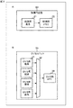
- FIG. 1 is a block diagram showing an outline of a system configuration of an image pickup apparatus according to the first embodiment of the present disclosure.
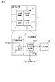
- FIG. 2A is a block diagram showing an example of the configuration of the gradation circuit
- FIG. 2B is a block diagram showing an example of the configuration of the DVS unit.
- FIG. 3 is a circuit diagram showing a specific example of the configuration of gradation pixels.
- FIG. 4 is a circuit diagram showing a specific example of the configuration of DVS pixels.
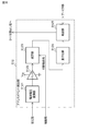
- FIG. 5 is a block diagram showing an example of the configuration of the address event detection unit.
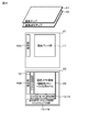
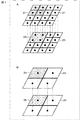
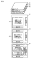
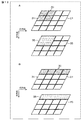
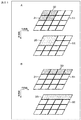
- FIG. 6 is a schematic view showing a laminated chip structure according to a specific example 1 in the image pickup apparatus according to the first embodiment of the present disclosure. A of FIG.
- FIG. 7 is a diagram showing a correspondence relationship 1 between the gradation pixels and DVS pixels of the semiconductor chip of the first layer and each analog front end portion of the semiconductor chip of the second layer
- B of FIG. 7 is a diagram. , The figure which shows the correspondence 2.
- FIG. 8 is an image diagram showing a pixel array of gradation pixels and DVS pixels.
- FIG. 9 is a schematic view showing a laminated chip structure according to a specific example 2 in the image pickup apparatus according to the first embodiment of the present disclosure.
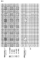
- FIG. 10A is a diagram showing a pixel arrangement according to a configuration example 1 in the image pickup apparatus according to the first embodiment of the present disclosure
- FIG. 10B is a diagram showing a pixel arrangement according to the configuration example 2.
- FIG. 11A is a diagram showing the pixel arrangement according to the configuration example 3 in the image pickup apparatus according to the first embodiment of the present disclosure
- FIG. 11B is a diagram showing the pixel arrangement according to the configuration example 4.
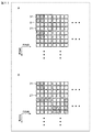
- a of FIG. 12 is a diagram showing an arrangement of a DVS unit according to an arrangement example 1 in the image pickup apparatus according to the first embodiment of the present disclosure and a connection relationship with an AFE for DVS
- B of FIG. 12 is an arrangement example 2. It is a figure which shows the arrangement of the DVS unit which concerns on
- FIG. 13 is a diagram showing an arrangement of a DVS unit according to an arrangement example 3 in the image pickup apparatus according to the first embodiment of the present disclosure and a connection relationship with an AFE for DVS, and B of FIG. 13 is an arrangement example 4. It is a figure which shows the arrangement of the DVS unit which concerns on
- 14A is a diagram showing an outline of the laminated chip structure according to the configuration example 1
- FIG. 14B is a diagram showing an outline of the laminated chip structure according to the configuration example 2.
- FIG. 15 is a diagram showing an outline of the laminated chip structure according to the configuration example 3.
- FIG. 16 is a block diagram showing an outline of the system configuration of the image pickup apparatus according to the second embodiment of the present disclosure.
- FIG. 17 is a circuit diagram showing an example of the configuration of a basic pixel circuit of distance measuring pixels.
- a of FIG. 18 is a schematic view showing a laminated chip structure according to a specific example 1 in the image pickup apparatus according to the second embodiment of the present disclosure
- B of FIG. 18 is a schematic view showing a laminated chip structure according to the specific example 2.
- FIG. 19A is a diagram showing a pixel arrangement according to a configuration example 1 in the image pickup apparatus according to the second embodiment of the present disclosure
- FIG. 19B is a diagram showing a pixel arrangement according to the configuration example 2.
- FIG. 20A is a diagram showing a pixel arrangement according to a configuration example 3 in the image pickup apparatus according to the second embodiment of the present disclosure
- FIG. 20B is a diagram showing a pixel arrangement according to the configuration example 4.
- a of FIG. 21 is a diagram showing an arrangement of a DVS unit according to an arrangement example 1 in an image pickup apparatus according to a second embodiment of the present disclosure and a connection relationship with an AFE for DVS, and B of FIG. 21 is an arrangement example 2. It is a figure which shows the arrangement of the DVS unit which concerns on
- a of FIG. 22 is a diagram showing an arrangement of a DVS unit according to an arrangement example 3 in an image pickup apparatus according to a second embodiment of the present disclosure and a connection relationship with an AFE for DVS, and B of FIG. 22 is an arrangement example 4. It is a figure which shows the arrangement of the DVS unit which concerns on
- FIG. 23 is a block diagram showing an outline of the system configuration of the image pickup apparatus according to the third embodiment of the present disclosure.
- Specific example 1 (example of two-layer structure) 2-2-2.
- Specific example 2 (example of three-layer structure) 2-3.
- Configuration example of pixel array section 2-3-1 Configuration Example 1 (Example of arranging units composed of gradation pixels and DVS pixels side by side according to a predetermined rule) 2-3-2.
- Configuration Example 2 (Example of arranging units including pixels for DVS side by side in units of pixel rows) 2-3-3.
- Configuration Example 3 (Example of arranging units including pixels for DVS side by side in units of pixel rows) 2-3-4.
- Configuration example 4 (example of arranging DVS units irregularly) 2-4.
- Arrangement example 1 (an example in which DVS units are arranged in a square and consist of four DVS pixels) 2-4-2.
- Arrangement example 2 (an example in which DVS units are arranged side by side in the row direction and consist of four DVS pixels) 2-4-3.
- Arrangement example 3 (an example in which DVS units are arranged side by side in the column direction and consist of four DVS pixels) 2-4-4.
- Arrangement example 4 (Example in which the size of the DVS unit is larger than the size of the gradation pixel) 2-5.
- Configuration example of laminated chip structure 1 (configuration example of global shutter function) 2-5-2.
- Configuration example of laminated chip structure 2 (configuration example of readout function) 2-5-3.
- Configuration example 3 of laminated chip structure (configuration example of area AD) 2-6.
- Imaging device according to the second embodiment (event pixel + ranging pixel) 3-1.
- System configuration example 3-2. Laminated chip structure 3-2-1.
- Specific Example 1 (Example of mounting a SPAD element on the upper chip and mounting a quench circuit on the lower chip) 3-2-2.
- Specific Example 2 (Example in which a quench circuit and a time measuring unit are mounted on the lower chip with a plurality of SPAD elements on the upper chip as a unit) 3-3.
- Configuration Example 1 (Example of arranging units composed of DVS pixels and ranging pixels in a matrix) 3-3-2.
- Configuration Example 2 (Example of arranging units including pixels for DVS side by side in units of pixel rows) 3-3-3.
- Configuration Example 3 (Example of arranging units including pixels for DVS side by side in units of pixel rows) 3-3-4.
- Configuration example 4 (example of randomly arranging DVS units) 3-4.
- Imaging device according to the third embodiment (event pixel + gradation pixel + ranging pixel) 5.
- the event pixel units when a predetermined number of event pixels are used as event pixel units, the event pixel units may be arranged side by side in the pixel array unit according to a predetermined rule. can.
- the event pixel unit may be configured to be arranged in the pixel array unit by combining a predetermined number of gradation pixels with the pixel unit. .. Further, the event pixel unit may be arranged side by side in a pixel row unit or a pixel column unit in the matrix-shaped pixel array of the pixel array unit.
- the event pixel units are irregularly arranged in the pixel array unit.
- the event pixels may be arranged side by side in the event pixel unit according to a predetermined rule. Specifically, the event pixels are arranged in a square, in the row direction of a matrix-like pixel array, or in a column direction in the event pixel unit. Can be done.
- the size of the event pixel may be larger than the size of the gradation pixel. Further, the number of gradation pixels can be larger than the number of event pixels.
- the pixel array unit includes reflection from the distance measuring object based on the irradiation light from the light source unit in addition to the event pixel and the gradation pixel. It is possible to have a configuration in which distance measuring pixels including a light receiving element that receives light and generates a signal in response to the light received by a photon are mixed.
- the semiconductor chip on the second layer may be provided with a quench circuit for controlling the light receiving element corresponding to the distance measuring pixels.
- the light receiving element of the distance measuring pixel is composed of an avalanche photodiode operating in the Geiger mode, preferably a single photon avalanche diode. can do.
- the image pickup apparatus has a laminated chip structure in which at least two semiconductor chips, a semiconductor chip of the first layer and a semiconductor chip of the second layer, are laminated.
- the pixel array unit provided on the first-layer semiconductor chip is configured by mixing event pixels and gradation pixels.
- the event pixel is a pixel that detects an event in which the amount of change in the brightness of the pixel exceeds a predetermined threshold value as an event occurrence and outputs an event detection signal.
- the event pixels are used in a non-scanning type (asynchronous type) image pickup device called DVS. Therefore, in the following, the event pixel may be described as a DVS pixel.
- the gradation pixel outputs a pixel signal having a gradation level according to the amount of incident light.
- FIG. 1 is a block diagram showing an outline of a system configuration of an image pickup apparatus according to the first embodiment of the present disclosure.
- the image pickup apparatus 10A has a pixel array unit 11, an access control unit 12, a DVS reading unit 13, a column signal processing unit 14, a DVS signal processing unit 15, and a gradation signal processing. It has a configuration including a unit 16, a timing control unit 17, a time stamp generation unit 18, and output interfaces (I / F) 19A and 19B.
- the pixel array unit 11 is provided with a gradation circuit 20 and a DVS unit 30 which is an event pixel unit in a mixed state.
- the gradation circuit 20 includes a gradation pixel 21 and a gradation memory 22 for storing a pixel signal output from the gradation pixel 21.
- the DVS unit 30 has a predetermined number of DVS pixels 31, for example, four DVS pixels 31 as a unit.
- the DVS unit 30 processes the selector 32 that selects the event detection signal output from the four DVS pixels 31 and the event detection signal selected by the selector 32. It has an AFE (analog front end) 35 for DVS.
- the access control unit 12 outputs various drive signals to each gradation pixel 21 of the pixel array unit 11 when reading a pixel signal having a gradation level corresponding to the amount of incident light from the gradation pixel 21. Further, when reading the event detection signal from the DVS pixel 31, the access control unit 12 outputs a row drive signal to each DVS pixel 31 of the pixel array unit 11.
- the DVS reading unit 13 reads an event detection signal from each DVS pixel 31 of the pixel array unit 11 under the drive of the access control unit 12, and uses the read event detection signal as event data in the DVS signal processing unit 15. Supply.
- the column signal processing unit 14 has, for example, an analog-digital converter for the number of pixel rows provided for each pixel row of the gradation pixel 21, and the pixel array unit 11 is driven by the access control unit 12.
- the analog pixel signal (gradation brightness signal) read from each gradation pixel 21 is converted into a digital pixel signal and supplied to the gradation signal processing unit 16.
- the DVS signal processing unit 15 outputs the event detection signal read from each DVS pixel 31 of the pixel array unit 11 after the DVS reading unit 13 performs signal processing such as adding a time stamp, which will be described later. It is output as event data to the outside of the image pickup apparatus 10A via the interface (I / F) 19A.
- the gradation signal processing unit 16 performs signal processing such as CDS (Correlated Double Sampling) processing and time stamping, which will be described later, on the digital pixel signal output from the column signal processing unit 14. After the application, the data is output as gradation data to the outside of the image pickup apparatus 10A via the output interface (I / F) 19B.
- CDS Correlated Double Sampling
- time stamping which will be described later
- the timing control unit 17 generates various timing signals, clock signals, control signals, and the like, and performs drive control of the DVS signal processing unit 15, the gradation signal processing unit 16, and the like based on the generated signals. ..
- the time stamp generation unit 18 represents the relative time of the output timing of the event data and the pixel data with respect to the event data output from the DVS reading unit 13 and the pixel data output from the column signal processing unit 14. Generate a time stamp (time information). The generated time stamp is added to the event data in the DVS signal processing unit 15 and to the pixel data in the gradation signal processing unit 16.
- FIG. 3 is a circuit diagram showing a specific example of the configuration of the gradation pixel 21.
- the gradation pixel 21 has, for example, a photodiode 211 as a photoelectric conversion element.
- the gradation pixel 21 has a transfer transistor 212, a reset transistor 213, an amplification transistor 214, and a selection transistor 215.
- an N-type MOS type field effect transistor FET is used as the four transistors of the transfer transistor 212, the reset transistor 213, the amplification transistor 214, and the selection transistor 215.
- FET field effect transistor
- the combination of the conductive types of the four transistors 212 to 215 exemplified here is only an example, and is not limited to these combinations.
- a plurality of pixel control lines are commonly wired to each gradation pixel 21 in the same pixel row for the gradation pixel 21. These plurality of pixel control lines are connected to the output end corresponding to each pixel row of the access control unit 12 shown in FIG. 1 in pixel row units.
- various drive signals specifically, transfer signals for a plurality of pixel control lines.
- the TRG, the reset signal RST, and the selection signal SEL are output as appropriate.
- the anode electrode is connected to a low-potential side power supply (for example, ground), and the received light is photoelectrically converted into a light charge (here, a photoelectron) having a charge amount corresponding to the light amount, and the light thereof is converted. Accumulates electric charge.
- the cathode electrode of the photodiode 211 is electrically connected to the gate electrode of the amplification transistor 214 via the transfer transistor 212.
- the region in which the gate electrode of the amplification transistor 214 is electrically connected is a floating diffusion (floating diffusion region / impurity diffusion region) FD.
- the floating diffusion FD is a charge-voltage conversion unit that converts electric charge into voltage.
- a transfer signal TRG in which a high level (for example, V DD level) is active is given to the gate electrode of the transfer transistor 212 by the access control unit 12.
- the transfer transistor 212 becomes conductive in response to the transfer signal TRG, is photoelectrically converted by the photodiode 211, and transfers the optical charge stored in the photodiode 211 to the floating diffusion FD.
- the reset transistor 213 is connected between the node of the high potential side power supply voltage V DD and the floating diffusion FD.
- a reset signal RST that activates a high level is given to the gate electrode of the reset transistor 213 by the access control unit 12.
- the reset transistor 213 becomes conductive in response to the reset signal RST, and resets the floating diffusion FD by discarding the charge of the floating diffusion FD to the node of the voltage V DD.
- the gate electrode is connected to the floating diffusion FD, and the drain electrode is connected to the node of the high potential side power supply voltage VDD.
- the amplification transistor 214 serves as an input unit for a source follower that reads out a signal obtained by photoelectric conversion in the photodiode 211. That is, in the amplification transistor 214, the source electrode is connected to the signal line VSL via the selection transistor 215.
- the amplification transistor 214 and the load current source I connected to one end of the signal line VSL form a source follower that converts the voltage of the floating diffusion FD into the potential of the signal line VSL.
- the drain electrode is connected to the source electrode of the amplification transistor 214, and the source electrode is connected to the signal line VSL.
- a selection signal SEL that activates a high level is given to the gate electrode of the selection transistor 215 from the access control unit 12.
- the selection transistor 215 enters a conduction state in response to the selection signal SEL, so that the signal output from the amplification transistor 214 is transmitted to the signal line VSL with the gradation pixel 21 as the selection state.
- the circuit configuration of the gradation pixel 21 is an example of a 4Tr configuration including a transfer transistor 212, a reset transistor 213, an amplification transistor 214, and a selection transistor 215, that is, four transistors (Tr).
- the selection transistor 215 may be omitted, and the amplification transistor 214 may have a 3Tr configuration in which the function of the selection transistor 215 is provided. If necessary, the number of transistors may be increased to form a circuit configuration of 5Tr or more. can.
- FIG. 4 is a circuit diagram showing a specific example of the configuration of the DVS pixel 31.
- Each of the plurality of (for example, four) DVS pixels 31 constituting the DVS unit 30 has a photoelectric conversion unit 311 and an address event detection unit 312.
- An arbiter portion 34 is provided as one of the peripheral circuits of the DVS pixel 31.
- the arbiter unit 34 arbitrates the requests from each of the plurality of DVS pixels 31, and transmits a response based on the arbitration result to the DVS pixels 31.
- the photoelectric conversion unit 311 has a photoelectric conversion element (light receiving element) 3111 and a control transistor 3112.
- the control transistor 3112 for example, an N-type MOS (Metal Oxide Semiconductor) transistor can be used.
- the photoelectric conversion element (light receiving element) 3111 photoelectrically converts the incident light to generate an electric charge having an electric charge corresponding to the amount of the incident light.
- a transfer signal TRG is supplied to the gate electrode of the control transistor 3112, for example, from the access control unit 12 (see FIG. 1).
- the control transistor 3112 supplies the charge photoelectrically converted by the photoelectric conversion element 3111 to the address event detection unit 312 in response to the transfer signal TRG.
- the address event detection unit 312 determines whether or not an address event (hereinafter, may be simply referred to as “event”) has occurred depending on whether or not the amount of change in the photocurrent from the photoelectric conversion unit 3111 exceeds a predetermined threshold value. To detect.
- the address event includes, for example, an on-event indicating that the amount of change in the photocurrent exceeds the upper limit threshold value and an off-event indicating that the amount of change in the photocurrent has fallen below the lower limit threshold value.
- the event data (event detection signal) indicating the detection result of the address event is composed of, for example, one bit indicating the detection result of the on event and one bit indicating the detection result of the off event.
- the address event detection unit 312 When an address event occurs, the address event detection unit 312 supplies a request for transmitting an event detection signal to the arbiter unit 34. Then, when the address event detection unit 312 receives the response to the request from the arbiter unit 34, the address event detection unit 312 supplies the event detection signal (event data) to the DVS reading unit 13.
- FIG. 5 is a block diagram showing an example of the configuration of the address event detection unit 312. As shown in FIG. 5, the address event detection unit 312 according to this configuration example has a current / voltage conversion unit 3121, a buffer 3122, a subtractor 3123, a quantizer 3124, and a transfer unit 3125.
- the current-voltage conversion unit 3121 converts the photocurrent from the photoelectric conversion unit 311 of the DVS pixel 31 into a logarithmic voltage signal.
- the current-voltage conversion unit 3121 supplies the voltage signal converted by the current-voltage conversion unit 3121 to the buffer 3122.
- the buffer 3122 buffers the voltage signal supplied from the current-voltage conversion unit 3121 and supplies it to the subtractor 3123.
- a row drive signal is supplied to the subtractor 3123 from the access control unit 12 (see FIG. 1).
- the subtractor 3123 reduces the level of the voltage signal supplied from the buffer 3122 according to the row drive signal. Then, the subtractor 3123 supplies the voltage signal after the level drop to the quantizer 3124.
- the quantizer 3124 quantizes the voltage signal supplied from the subtractor 3123 into a digital signal and outputs it to the transfer unit 3125 as an event detection signal (event data).
- the transfer unit 3125 transfers the event detection signal (event data) supplied from the quantizer 3124 to the arbiter unit 34 or the like.
- the transfer unit 3125 supplies a request for transmitting an event detection signal to the arbiter unit 34.
- the transfer unit 3125 receives the response to the request from the arbiter unit 34, the transfer unit 3125 supplies the event detection signal (event data) to the DVS reading unit 13.
- the DVS reading unit 13 Regarding the reading of the event data from the DVS pixel 31, it is also possible to read a plurality of lines.
- the image pickup apparatus 10A has a laminated chip structure in which at least two semiconductor chips, a semiconductor chip of the first layer and a semiconductor chip of the second layer, are laminated. A specific example of the laminated chip structure will be described below.
- Specific example 1 is an example in which the laminated chip structure has a two-layer structure.
- FIG. 6 shows a schematic diagram of the laminated chip structure according to the specific example 1.
- the laminated chip structure according to the first embodiment is a two-layer structure in which the first-layer semiconductor chip 41 and the second-layer semiconductor chip 42 are laminated.
- the semiconductor chip 41 on the first layer is provided with a pixel array unit 11 in which the gradation pixels 21 and the DVS pixels 31 are mixed. That is, the semiconductor chip 41 of the first layer is a pixel chip provided with the gradation pixel 21 and the DVS pixel 31.
- the second-layer semiconductor chip 42 is provided with a pixel AFE (analog front end) region 44 corresponding to the pixel array unit 11 of the first-layer semiconductor chip 41.
- the pixel AFE region 44 includes an analog front-end portion for the gradation pixel 21 including the gradation memory 22 (see A in FIG. 2), and a DVS pixel including the DVS AFE35 (see B in FIG. 2).
- An analog front end portion for 31 is provided corresponding to the gradation pixel 21 and the DVS pixel 31. That is, the second-layer semiconductor chip 42 is a pixel AFE chip provided with the pixel AFE region 44.
- the second layer semiconductor chip 42 further has an access control unit 12, a DVS reading unit 13, a column signal processing unit 14, a DVS signal processing unit 15, and a gradation signal processing unit 16 in the peripheral region of the pixel AFE region 44. , A timing control unit 17, a time stamp generation unit 18, and the like are provided.
- the gradation pixels 21 and DVS pixels 31 of the first-layer semiconductor chip 41 and the analog front-end portions of the second-layer semiconductor chip 42 are metal-metal junctions including Cu-Cu junctions and through silicon vias. It is electrically connected via junctions 45A and 45B made of electrodes (Through Silicon Via: TSV), micro bumps, and the like.
- the correspondence with the analog front end portion 35 for the pixel 31 for DVS will be described.
- FIG. 7A is a diagram showing the correspondence 1 between the gradation pixel 21 and the DVS pixel 31 of the first layer semiconductor chip 41 and the analog front end portions 25 and 35 of the second layer semiconductor chip 42. be.
- the DVS unit 30 is configured in the semiconductor chip 41 of the first layer, for example, with four DVS pixels 31 as a unit.
- the DVS pixel 31 is associated with the analog front end unit 35 for the DVS pixel 31 in the unit of the DVS unit 30.
- the gradation pixel 21 is associated with the analog front end portion 25 for the gradation pixel 21 on a one-to-one basis.
- FIG. 7B is a diagram showing the correspondence relationship 2 between the gradation pixel 21 and the DVS pixel 31 of the first layer semiconductor chip 41 and the analog front end portions 25 and 35 of the second layer semiconductor chip 42. be.
- the DVS unit 30 in the semiconductor chip 41 of the first layer, for example, the DVS unit 30 is composed of four DVS pixels 31, and correspondingly, the gradation pixel 21 also has four.
- the gradation pixel unit 24 is configured in units of pixels. Then, between the semiconductor chip 41 of the first layer and the semiconductor chip 42 of the second layer, the gradation pixel unit 24 and the DVS unit 30 and the analog front end portions 25 and 35 are arranged one-to-one in unit units. It is associated with.
- FIG. 8 shows an image diagram of a pixel array of the gradation pixel 21 and the DVS pixel 31.
- the Bayer arrangement of R (red) / G (green) / B (blue) is exemplified for the gradation pixel 21 of the first layer semiconductor chip 41 which is the upper chip.
- the DVS pixels 31 are partially arranged in the pixel array of the Bayer array of R / Gr / Gb / B.
- the number of gradation pixels 21 is larger than the number of DVS pixels 31 which are event pixels. In this way, by arranging a larger number of gradation pixels 21 than the DVS pixels 31, it is possible to improve the image quality of the gradation data.
- the analog front end portion 35 for the DVS pixel 31 is shared by the four DVS pixels 31 of vertical 2 ⁇ horizontal 2, and is used for the gradation pixel 21.
- the analog front end portion 25 is electrically connected to the gradation pixel 21 of the upper chip in pixel units to realize a global shutter in the voltage domain.
- Specific example 2 is an example in which the laminated chip structure has a three-layer structure.
- FIG. 9 shows a schematic diagram of the laminated chip structure according to Specific Example 2.
- the laminated chip structure according to the second embodiment is a three-layer structure in which the first-layer semiconductor chip 41, the second-layer semiconductor chip 42, and the third-layer semiconductor chip 43 are laminated. It has become.
- the semiconductor chip 41 on the first layer is provided with a pixel array unit 11 in which the gradation pixels 21 and the DVS pixels 31 are mixed. That is, the semiconductor chip 41 of the first layer is a pixel chip provided with the gradation pixel 21 and the DVS pixel 31.
- the second-layer semiconductor chip 42 is provided with a pixel AFE (analog front end) region 44 corresponding to the pixel array unit 11 of the first-layer semiconductor chip 41.
- the pixel AFE region 44 includes an analog front-end portion for the gradation pixel 21 including the gradation memory 22 (see A in FIG. 2), and a DVS pixel including the DVS AFE35 (see B in FIG. 2).
- An analog front end portion for 31 is provided corresponding to the gradation pixel 21 and the DVS pixel 31. That is, the second-layer semiconductor chip 42 is a pixel AFE chip provided with the pixel AFE region 44.
- the third layer semiconductor chip 43 includes an access control unit 12, a DVS reading unit 13, a column signal processing unit 14, a DVS signal processing unit 15, a gradation signal processing unit 16, a timing control unit 17, and a time stamp generation. A portion 18 and the like are provided.
- the first-layer semiconductor chip 41 and the second-layer semiconductor chip 42 are electrically connected via metal-metal joints including Cu-Cu joints, TSVs, microbumps, and other joint portions 45A and 45B.
- the second-layer semiconductor chip 42 and the third-layer semiconductor chip 43 are electrically connected via metal-metal joints including Cu-Cu joints, TSVs, microbumps, and other joint portions 45B and 45C. Will be done.
- the two-layer structure and the three-layer structure are exemplified as the laminated chip structure, but the structure is not limited to the two-layer structure and the three-layer structure, and a laminated chip structure having four or more layers is also possible. Is.
- Configuration example 1 of the pixel array unit 11 is an example in which units composed of gradation pixels 21 and DVS pixels 31 are arranged side by side in the pixel array unit 11 according to a predetermined rule.
- the pixel arrangement according to the configuration example 1 is shown in FIG. 10A.
- the pixel arrangement according to the configuration example 1 is, for example, 12 gradation pixels 21 having 4 pixels (R / Gr / Gb / B) as a unit and DVS having 4 DVS pixels 31 as a unit.
- the pixel units X in which the units 30 are arranged side by side in a square, are two-dimensionally arranged in a matrix. According to the pixel arrangement according to the configuration example 1, the gradation data and the event data can be associated with each unit.
- Configuration example 2 is an example in which units including DVS pixels 31 are arranged side by side in units of pixel rows. The pixel arrangement according to the configuration example 2 is shown in B of FIG.
- the pixel arrangement according to the configuration example 2 is, for example, 12 gradation pixels 21 having 4 pixels (R / Gr / Gb / B) as a unit and DVS having 4 DVS pixels 31 as a unit.
- Pixel units X in which the units 30 are arranged side by side in a square are arranged side by side in units of pixel rows.
- the pixel row in which the DVS pixel 31 does not exist that is, there is no defect
- Configuration example 3 is an example in which units including DVS pixels 31 are arranged side by side in units of pixel rows. The pixel arrangement according to the configuration example 3 is shown in FIG. 11A.
- the pixel arrangement according to the configuration example 3 is, for example, 12 gradation pixels 21 having 4 pixels (R / Gr / Gb / B) as a unit and DVS having 4 DVS pixels 31 as a unit.
- Pixel units X in which the units 30 are arranged side by side in a square are arranged side by side in units of pixel rows.
- the amount of event data included in the pixel row can be made uniform as compared with the case of the pixel arrangement according to the configuration example 2, so that the gradation data (R / G) with stable image quality can be arranged.
- / B data can be acquired. This point is the same in the case of the pixel arrangement according to the configuration example 1.
- Configuration example 4 is an example in which the DVS units 30 are arranged irregularly side by side. The pixel arrangement according to the configuration example 4 is shown in B of FIG.
- the DVS unit 30 having four DVS pixels 31 as a unit is randomly arranged, for example, four DVS pixels 31 are arranged in a square, or the row direction / column. It is configured to be arranged side by side in the direction. According to the pixel arrangement according to the configuration example 4, high-resolution data can be restored as in the compressed sensing.
- Arrangement example 1 is an example in which the DVS unit 30 is composed of four DVS pixels 31 arranged side by side in a square.
- the arrangement of the DVS unit 30 according to the arrangement example 1 and the connection relationship with the DVS AFE35 are shown in FIG. 12A.
- one DVS AFE35 having the size of four rectangular areas of the DVS pixel 31 is associated with the four DVS pixels 31 arranged side by side in a square. I try to connect electrically.
- Arrangement example 2 is an example in which the DVS units 30 are arranged side by side in the row direction and are composed of four DVS pixels 31.
- the arrangement of the DVS unit according to the arrangement example 2 and the connection relationship with the AFE35 for DVS are shown in B of FIG.
- the size of the horizontally long rectangular area of four DVS pixels 31 is large with respect to the four DVS pixels 31 arranged in a horizontally long rectangular shape arranged in the row direction.
- One DVS AFE35 is associated with each other and electrically connected.
- Arrangement example 3 is an example in which the DVS units 30 are arranged in a row direction and are composed of four DVS pixels 31.
- the arrangement of the DVS unit according to the arrangement example 3 and the connection relationship with the DVS AFE35 are shown in FIG. 13A.
- Arrangement Example 3 of the DVS unit 30 the size of the vertically long rectangular area of four DVS pixels 31 is large with respect to the four DVS pixels 31 arranged in a vertically long rectangular shape arranged in the column direction.
- One DVS AFE35 is associated with each other and electrically connected.
- Arrangement example 4 is an example in which the size of the DVS unit 30 is larger than the size of the gradation pixel 21.
- the arrangement of the DVS unit according to the arrangement example 4 and the connection relationship with the AFE35 for DVS are shown in B of FIG.
- the size of the DVS unit 30 is configured to be larger than the size of the gradation pixel 21, for example, the size of four DVS pixels 31 arranged side by side in a square. is doing.
- one DVS AFE35 having the same size as the DVS unit 30 is associated with the DVS unit 30 and electrically connected to the DVS unit 30.
- Configuration example 1 of the laminated chip structure is a configuration example of the global shutter function.
- the outline of the laminated chip structure according to the configuration example 1 is shown in FIG. 14A.
- the photodiode 211, the transfer transistor 212, and the buffer 216 are two-dimensionally arranged in a matrix for each pixel on the semiconductor chip 41 of the first layer, which is the upper chip.
- a data processing unit 217 or the like that processes a signal component (so-called D-phase data) and a reset component (so-called P-phase data) is mounted on the second-layer semiconductor chip 42, which is the lower chip, corresponding to the pixels. Will be done.
- Configuration example 2 of the laminated chip structure is a configuration example of the reading function.
- the outline of the laminated chip structure according to the configuration example 2 is shown in A of FIG.
- the photodiode 211 and the transfer transistor 212 are two-dimensionally arranged in a matrix for each pixel on the semiconductor chip 41 of the first layer, which is the upper chip.
- a reset transistor 213, an amplification transistor 214, a selection transistor 215, and the like are mounted on the second layer semiconductor chip 42, which is the lower chip, corresponding to the pixels.
- Configuration example 3 of the laminated chip structure is a configuration example of the area AD.
- FIG. 15 shows an outline of the laminated chip structure according to the configuration example 3.
- the gradation pixels 21 having the circuit configuration shown in FIG. 3 are two-dimensionally arranged in a matrix on the semiconductor chip 41 of the first layer, which is the upper chip.
- an analog-to-digital converter (ADC) 141 is mounted on the second-layer semiconductor chip 42, which is a lower chip, corresponding to the gradation pixels 21 arranged in two dimensions.
- ADC analog-to-digital converter
- the image pickup apparatus 10A according to the first embodiment has a configuration in which the gradation pixel 21 and the event pixel DVS pixel 31 are mixed in the pixel array unit 11. Therefore, according to the image pickup apparatus 10A according to the first embodiment, not only the event detection signal (event data) indicating the occurrence of an event but also the pixel signal (gradation data) having a gradation level according to the amount of incident light is obtained. Can be output.
- the image pickup apparatus 10A according to the first embodiment not only the event detection signal (event data) indicating the occurrence of an event but also the pixel signal (gradation data) having a gradation level according to the amount of incident light is obtained. Can be output.
- the image pickup apparatus 10A according to the first embodiment not only the event detection signal (event data) indicating the occurrence of an event but also the pixel signal (gradation data) having a gradation level according to the amount of incident light is obtained. Can be output.
- the gradation pixel 21 is used. Imaging can be realized
- the image pickup apparatus has a laminated chip structure in which at least two semiconductor chips, a semiconductor chip of the first layer and a semiconductor chip of the second layer, are laminated, and the semiconductor chip of the first layer is formed.
- the pixel array unit provided in the above is configured to have a mixture of event pixels and ranging pixels.
- the distance measuring pixel is a pixel including a light receiving element (photodetection element) that receives reflected light from a distance measuring object based on the irradiation light from the light source unit and generates a signal in response to the light reception of photons.
- a light receiving element that generates a signal in response to light reception of a photon
- a SPAD (Single Photon Avalanche Diode) element can be exemplified.
- the SPAD element operates in a region called Geiger mode where there is no DC-like stable point in which the element is operated with a reverse voltage exceeding the breakdown voltage (yield voltage).
- the SPAD element is exemplified here as the light receiving element of the pixel, it is not limited to the SPAD element. That is, as the light receiving element, in addition to the SPAD element, various elements operating in the Geiger mode such as APD (avalanche photodiode) and SiPM (silicon photomultiplier) can be used.
- APD active photodiode
- SiPM silicon photomultiplier
- FIG. 16 is a block diagram showing an outline of the system configuration of the image pickup apparatus according to the second embodiment of the present disclosure.
- the image pickup apparatus 10B includes a pixel array unit 11, an access control unit 12, a DVS reading unit 13, a DVS signal processing unit 15, a timing control unit 17, a time stamp generation unit 18, and an output interface (I). / F) In addition to 19A, it has a time-to-digital converter (TDC) 61, a distance measuring signal processing unit 62, and an output interface 19C.
- TDC time-to-digital converter
- the pixel array unit 11 is provided with a DVS unit 30 and a distance measuring pixel 50 in a mixed state.
- the DVS unit 30 it is possible to use the one having the configuration exemplified in the first embodiment (see B in FIG. 2) including the DVS pixel 31 which is an event pixel.
- FIG. 17 shows an example of the configuration of the basic pixel circuit of the distance measuring pixel 50.
- the distance measuring pixel 50 has, for example, a SPAD element 51 as a light receiving element, a quench circuit 52, and a readout circuit 53.
- the cathode electrode is connected to the first power supply, and the anode electrode is connected to the second power supply via the quench circuit 52.
- a large voltage at which avalanche multiplication occurs that is, a voltage equal to or higher than the breakdown voltage is applied to the cathode electrode of the SPAD element 51 from the first power supply.
- the quench circuit 52 stops the avalanche multiplication by lowering the voltage between the terminals of the SPAD element 51, that is, the voltage between the cathode electrode and the anode electrode, below the breakdown voltage of the PN diode. This operation is a so-called quenching operation.
- the readout circuit 53 is composed of, for example, a CMOS inverter circuit including a P-type MOS transistor Q p and an N-type MOS transistor Q n , and detects the reaction edge of the MOSFET element 51.
- the detection output of the readout circuit 53 is supplied to the time measurement unit (TDC) 61 shown in FIG. 16 as a SPAD output (pixel output).
- the image pickup apparatus 10B includes a pixel 31 for DVS, a configuration capable of acquiring event information, and a distance measuring element 51 including a SPAD element 51 that generates a signal in response to light reception of photons. It is equipped with a pixel 50 and is configured to be capable of measuring the distance to the object to be measured (subject).
- a measuring method for measuring the distance to the distance measuring object for example, ToF which measures the time until the light emitted from the light source unit toward the distance measuring object is reflected by the distance measuring object and returns.
- the (Time of Flight) method can be adopted.
- a light source unit 70 for irradiating light toward a distance measuring object is provided as an external device of the image pickup apparatus 10B according to the second embodiment.
- a distance measuring device (system) can be configured by combining the image pickup device 10B and the light source unit 70 according to the second embodiment.
- the light source unit 70 is composed of, for example, a semiconductor laser, and is driven by a laser drive unit (not shown) to irradiate a laser beam toward a measurement target (subject).
- the irradiation laser light from the light source unit 70 is reflected by the object to be measured (subject), and the reflected light is incident on the distance measuring pixel 50 including the SPAD element 51.
- the time measuring unit (TDC) 61 is based on the SPAD output output from the distance measuring pixel 50, and the time until the laser beam emitted toward the measurement object is reflected by the measurement object and returned. To measure.
- the time measurement is executed a plurality of times, and the time is measured by detecting the position of the peak of the ToF histogram obtained by accumulating the times measured a plurality of times.
- a method of measuring the time a method of measuring the time from the timing of irradiating the laser beam from the light source unit 70 toward the object to be measured to the timing of receiving the reflected light from the object to be measured by the distance measuring pixel 50 is used. It can be exemplified.
- pulsed light is irradiated from the light source unit 70 at a predetermined cycle, the cycle when the distance measuring pixel 50 receives the pulsed light is detected, and the emission cycle and the light receiving cycle are defined.
- a method of measuring time from a phase difference can be exemplified.
- the measurement result of the time measuring unit 61 is supplied to the distance measuring signal processing unit 62.
- the range-finding signal processing unit 62 performs predetermined signal processing on the measurement result of the time measurement unit 61, and then outputs the range-finding data via the output interface 19C.
- the image pickup apparatus 10B according to the second embodiment for convenience, the pixel array unit 11, the access control unit 12, the DVS reading unit 13, the time measuring unit 61, the DVS signal processing unit 15, and the distance measuring unit are used.
- the signal processing unit 62, the timing control unit 17, the time stamp generation unit 18, and the like are shown as a flat structure arranged in a plane.
- the image pickup apparatus 10B according to the second embodiment is formed by stacking at least two semiconductor chips, that is, a semiconductor chip of the first layer and a semiconductor chip of the second layer, similarly to the image pickup apparatus 10A according to the first embodiment. It has a laminated chip structure.
- the laminated chip structure is not limited to the two-layer structure, and the three or more layers are the same as in the case of the image pickup apparatus 10A according to the first embodiment. It is also possible to have a laminated chip structure of.
- Specific Example 1 is an example in which the SPAD element 51 is mounted on the semiconductor chip 41 of the first layer, which is the upper chip, and the quench circuit 52 is mounted on the semiconductor chip 42 of the second layer, which is the lower chip.
- a schematic diagram of the laminated chip structure according to Specific Example 1 is shown in FIG. 18A.
- the laminated chip structure according to the first embodiment it is a lower chip with respect to the SPAD element 51 arranged in an array on the first layer semiconductor chip 41 which is the upper chip.
- a quench circuit 52 and a read circuit 53 that control the quench operation of the SPAD element 51 are mounted on the semiconductor chip 42 of the second layer in a one-to-one correspondence.
- the quench circuit 52 and the time measuring unit (TDC) 61 are attached to the semiconductor chip 42 of the second layer, which is the lower chip, in units of the plurality of SPAD elements 51 on the semiconductor chip 41 of the first layer, which is the upper chip. This is an example of mounting.
- a schematic diagram of the laminated chip structure according to Specific Example 2 is shown in FIG. 18B.
- the lower chip is a unit of a plurality of SPAD elements 51 arranged in an array on the first layer semiconductor chip 41 which is the upper chip.
- the quench circuit 52, the readout circuit 53, and the time measurement unit (TDC) 61 are mounted on the second-layer semiconductor chip 42 with a one-to-one correspondence.
- Configuration example 1 of the pixel array unit 11 is an example in which units composed of the DVS pixels 31 and the SPAD element 51 are arranged in a matrix.
- the pixel arrangement according to the configuration example 1 is shown in A of FIG.
- a pixel unit X in which four DVS pixels 31 and a DVS unit 30 having 12 SPAD elements 51 as a unit are arranged side by side in a square is formed in a matrix. It has a two-dimensional arrangement. According to the pixel arrangement according to the configuration example 1, the distance measurement data and the event data can be associated with each unit.
- Configuration example 2 is an example in which units including DVS pixels 31 are arranged side by side in units of pixel rows. The pixel arrangement according to the configuration example 2 is shown in B of FIG.
- a pixel unit X in which four DVS pixels 31 and a DVS unit 30 having 12 SPAD elements 51 as a unit are arranged in a square is arranged in a pixel row. It is configured to be arranged side by side in units. According to the pixel arrangement according to the configuration example 2, when the SPAD element 51 is accessed, the pixel row in which the DVS pixel 31 does not exist (that is, there is no defect) can be selected.
- Configuration Example 3 is an example in which units including DVS pixels 31 are arranged side by side in units of pixel rows. The pixel arrangement according to the configuration example 3 is shown in FIG. 20A.
- a pixel unit X in which four DVS pixels 31 and a DVS unit 30 having 12 SPAD elements 51 as a unit are arranged in a square are arranged in a pixel row. It is configured to be arranged side by side in units.
- the amount of event data included in the pixel row can be made uniform as compared with the case of the pixel arrangement according to the configuration example 2, so that the gradation data (R / G) with stable image quality can be arranged. / B data) can be acquired. This point is the same in the case of the pixel arrangement according to the configuration example 1.
- Configuration example 4 is an example in which the DVS units 30 are randomly arranged.
- the pixel arrangement according to the configuration example 4 is shown in B of FIG.
- the DVS unit 30 having four DVS pixels 31 as a unit is randomly arranged, for example, four DVS pixels 31 are arranged in a square, or the row direction / column. It is configured to be arranged side by side in the direction. According to the pixel arrangement according to the configuration example 4, high-resolution data can be restored as in the compressed sensing.
- Arrangement example 1 is an example in which the DVS unit 30 is composed of four DVS pixels 31 arranged side by side in a square.
- the arrangement of the DVS unit 30 according to the arrangement example 1 and the connection relationship with the DVS AFE35 are shown in FIG. 21A.
- one DVS AFE35 having the size of four rectangular areas of the DVS pixel 31 is associated with the four DVS pixels 31 arranged side by side in a square. I try to connect electrically.
- Arrangement example 2 is an example in which the DVS units 30 are arranged side by side in the row direction and are composed of four DVS pixels 31.
- the arrangement of the DVS unit according to the arrangement example 2 and the connection relationship with the DVS AFE35 are shown in FIG. 21B.
- the size of the horizontally long rectangular area of four DVS pixels 31 is large with respect to the four DVS pixels 31 arranged in a horizontally long rectangular shape arranged in the row direction.
- One DVS AFE35 is associated with each other and electrically connected.
- Arrangement example 3 is an example in which the DVS units 30 are arranged in a row direction and are composed of four DVS pixels 31.
- the arrangement of the DVS unit according to the arrangement example 3 and the connection relationship with the DVS AFE35 are shown in FIG. 22A.
- Arrangement Example 3 of the DVS unit 30 the size of the vertically long rectangular area of four DVS pixels 31 is large with respect to the four DVS pixels 31 arranged in a vertically long rectangular shape arranged in the column direction.
- One DVS AFE35 is associated with each other and electrically connected.
- the arrangement example 4 is an example in which the size of the DVS unit 30 is larger than the size of the distance measuring pixel 50 including the SPAD element 51.
- the arrangement of the DVS unit according to the arrangement example 4 and the connection relationship with the DVS AFE35 are shown in FIG. 22B.
- the size of the DVS unit 30 is larger than the size of the distance measuring pixel 50 including the SPAD element 51, for example, four DVS pixels 31 arranged side by side in a square. It is configured as a size of size.
- one DVS AFE35 having the same size as the DVS unit 30 is associated with the DVS unit 30 and electrically connected to the DVS unit 30.
- the image pickup apparatus 10B according to the second embodiment has a configuration in which a DVS pixel 31 which is an event pixel and a distance measuring pixel 50 including a SPAD element 51 are mixed. Therefore, according to the image pickup apparatus 10B according to the second embodiment, it is possible to output not only event data indicating the occurrence of an event but also distance measurement data which is distance information to a measurement object (subject). As a result, for example, a moving object is detected by the pixel 31 for DVS, and only the detected moving object is subjected to distance measurement based on the distance measurement data, as compared with the case where distance measurement is performed for all subjects. , It is possible to realize distance measurement with low power consumption.
- the image pickup apparatus has a laminated chip structure in which at least two semiconductor chips, a semiconductor chip of the first layer and a semiconductor chip of the second layer, are laminated, and the semiconductor chip of the first layer is formed.
- the pixel array unit provided in the above, event pixels, gradation pixels, and distance measuring pixels are mixed. That is, the image pickup apparatus according to the third embodiment of the present disclosure has a configuration in which the configuration of the image pickup apparatus according to the first embodiment and the configuration of the image pickup apparatus according to the second embodiment are combined.
- FIG. 23 is a block diagram showing an outline of the system configuration of the image pickup apparatus according to the third embodiment of the present disclosure.
- the image pickup apparatus 10C according to the third embodiment includes a pixel array unit 11, an access control unit 12, a DVS reading unit 13, a column signal processing unit 14, a DVS signal processing unit 15, a gradation signal processing unit 16, and a timing control unit 17. , A time stamp generation unit 18, and output interfaces 19A and 19B.
- the image pickup apparatus 10C according to the third embodiment further includes a time measurement unit (TDC) 61, a distance measurement signal processing unit 62, and an output interface 19C.
- TDC time measurement unit
- 62 distance measurement signal processing unit
- output interface 19C This is the configuration of the image pickup apparatus 10B according to the second embodiment shown in FIG.
- the image pickup apparatus 10C according to the third embodiment includes a DVS pixel 31 which is an event pixel, a DVS pixel 31 which is an event pixel, and a distance measuring pixel 50 including a SPAD element 51. It has a mixed structure. Therefore, according to the image pickup apparatus 10C according to the third embodiment, not only the event data indicating the occurrence of the event but also the pixel signal (gradation data) of the gradation level according to the amount of incident light and the measurement object. Distance measurement data, which is distance information to (subject), can be output.
- the action and effect of the first embodiment and the action and effect of the second embodiment can be obtained.
- the gradation pixel 21 can be used without motion blur even in a dark environment.
- imaging such as acquiring gradation data having excellent S / N.
- the distance is measured for all subjects as compared with the case where the distance is measured. Distance measurement with low power consumption can be realized.
- the technique according to the present disclosure has been described above based on the preferred embodiment, the technique according to the present disclosure is not limited to the embodiment.
- the configuration and structure of the image pickup apparatus according to the third embodiment in which the pixels for gradation, the pixels for gradation, and the pixels for distance measurement are mixed are examples, and can be changed as appropriate.
- the image pickup device according to the first embodiment, the image pickup device according to the second embodiment, or the image pickup device according to the third embodiment has various types of sensing light such as visible light, infrared light, ultraviolet light, and X-ray. Can be used for equipment. Specific examples of various devices are listed below.
- Devices that take images for viewing such as digital cameras and portable devices with camera functions.
- Devices used for traffic such as in-vehicle sensors that capture images of the rear, surroundings, and interior of vehicles, surveillance cameras that monitor traveling vehicles and roads, and distance measuring sensors that measure distance between vehicles.
- Equipment used in home appliances such as TVs, refrigerators, and air conditioners to take pictures and operate the equipment according to the gestures ⁇ Endoscopes, devices that perform angiography by receiving infrared light, etc.
- Equipment used for medical and healthcare purposes ⁇ Equipment used for security such as surveillance cameras for crime prevention and cameras for person authentication ⁇ Skin measuring instruments for taking pictures of the skin and taking pictures of the scalp Equipment used for beauty such as microscopes ⁇ Equipment used for sports such as action cameras and wearable cameras for sports applications ⁇ Camera for monitoring the condition of fields and crops, etc.
- Equipment used for agriculture ⁇ Equipment used for medical and healthcare purposes
- Equipment used for security such as surveillance cameras for crime prevention and cameras for person authentication
- Skin measuring instruments for taking pictures of the skin and taking pictures of the scalp Equipment used for beauty such as microscopes
- Equipment used for sports such as action cameras and wearable cameras for sports applications
- Camera for monitoring the condition of fields and crops, etc.
- Equipment used for agriculture ⁇ Equipment used for agriculture
- the present disclosure may also have the following configuration.
- A. Imaging device ⁇ [A-01] It has a laminated chip structure in which at least two semiconductor chips, a semiconductor chip of the first layer and a semiconductor chip of the second layer, are laminated. In the semiconductor chip of the first layer, an event in which the amount of change in the brightness of the pixel exceeds a predetermined threshold value is detected as the occurrence of an event, and the event pixel that outputs the event detection signal and the amount of incident light correspond to the light amount.
- a pixel array section is provided in which gradation pixels that output gradation level pixel signals are mixed.
- the analog front-end portion of the event pixel that processes the event detection signal and the analog front-end portion of the gradation pixel that processes the pixel signal are the event pixel and the gradation pixel, respectively. It is provided corresponding to Imaging device.
- the event pixel units are arranged side by side in the pixel array unit according to a predetermined rule.
- the image pickup apparatus according to the above [A-01].
- the event pixel unit is arranged in the pixel array unit as a pixel unit in combination with a predetermined number of gradation pixels.
- the event pixel units are arranged side by side in units of pixel rows in the matrix-like pixel array of the pixel array unit.
- the event pixel units are arranged side by side in a pixel array unit in the matrix-like pixel array of the pixel array unit.
- [A-06] When a predetermined number of event pixels are used as an event pixel unit, The event pixel units are arranged irregularly in the pixel array section.
- [A-07] The event pixels are arranged side by side in the event pixel unit according to a predetermined rule.
- the image pickup apparatus according to the above [A-02].
- A-08 The event pixels are arranged side by side in a square in the event pixel unit.
- A-09 The event pixels are arranged side by side in the row direction of the matrix-shaped pixel array in the event pixel unit.
- A-10 The event pixels are arranged side by side in the column direction of the matrix-shaped pixel array in the event pixel unit.
- [A-11] The size of the event pixel is larger than the size of the gradation pixel.
- the number of gradation pixels is larger than the number of event pixels.
- the imaging device according to any one of the above [A-01] to the above [A-11].
- the pixel array unit receives reflected light from the distance measuring object based on the irradiation light from the light source unit, and receives a signal in response to the light reception of photons. Pixels for distance measurement including light receiving elements that are generated are mixed.
- the image pickup apparatus according to the above [A-01].
- a quench circuit for controlling a light receiving element is provided on the second layer semiconductor chip corresponding to the distance measuring pixel.
- the image pickup apparatus according to the above [A-13].
- the light receiving element of the distance measuring pixel is composed of an avalanche photodiode operating in Geiger mode.
- the light receiving element of the distance measuring pixel is composed of a single photon avalanche diode.
- Imaging devices ⁇ [B-01] It has a laminated chip structure in which at least two semiconductor chips, a semiconductor chip of the first layer and a semiconductor chip of the second layer, are laminated.
- an event in which the amount of change in the brightness of the pixel exceeds a predetermined threshold value is detected as an event occurrence, and the event pixel that outputs the event detection signal and the irradiation light from the light source unit are used.
- a pixel array unit is provided in which distance measuring pixels including a light receiving element that receives reflected light from a distance measuring object and generates a signal in response to light received by a photon are mixed.
- the analog front-end portion of the event pixel that processes the event detection signal and the analog front-end portion of the distance measuring pixel that processes the signal of the light receiving element are the event pixel and the distance measuring. It is provided corresponding to each of the pixels.
- Imaging device. [B-02] The semiconductor chip on the second layer is provided with a quench circuit for controlling a light receiving element corresponding to the distance measuring pixel.
- the light receiving element of the distance measuring pixel is composed of an avalanche photodiode operating in Geiger mode.
- the light receiving element of the distance measuring pixel is composed of a single photon avalanche diode.
- DVS AFE analog front end
- 41 ... 1 Phase semiconductor chip 42 ... 2nd phase semiconductor chip, 43 ... 3rd phase semiconductor chip, 50 ... ranging circuit, 51 ... SPAD element, 52 ... quench circuit , 53 ... Read circuit, 61 ... Time measurement unit (TDC), 62 ... Distance measurement signal processing unit, 70 ... Light source unit
Landscapes
- Engineering & Computer Science (AREA)
- Multimedia (AREA)
- Signal Processing (AREA)
- Physics & Mathematics (AREA)
- Computer Networks & Wireless Communication (AREA)
- General Physics & Mathematics (AREA)
- Radar, Positioning & Navigation (AREA)
- Remote Sensing (AREA)
- Electromagnetism (AREA)
- Solid State Image Pick-Up Elements (AREA)
- Transforming Light Signals Into Electric Signals (AREA)
Abstract
Description
1層目の半導体チップ及び2層目の半導体チップの少なくとも2つの半導体チップが積層されて成る積層チップ構造を有し、
1層目の半導体チップには、画素の輝度変化量が所定の閾値を超えた事象を、イベントの発生として検出し、イベント検出信号を出力するイベント用画素、及び、入射光の光量に応じた階調レベルの画素信号を出力する階調用画素が混在する画素アレイ部が設けられており、
2層目の半導体チップには、イベント検出信号を処理するイベント用画素のアナログフロントエンド部、及び、画素信号を処理する階調用画素のアナログフロントエンド部が、イベント用画素及び階調用画素のそれぞれに対応して設けられている。
1層目の半導体チップ及び2層目の半導体チップの少なくとも2つの半導体チップが積層されて成る積層チップ構造を有し、
1層目の半導体チップには、画素の輝度変化量が所定の閾値を超えた事象を、イベントの発生として検出し、イベント検出信号を出力するイベント用画素、及び、光源部からの照射光に基づく、測距対象物からの反射光を受光し、光子の受光に応じて信号を発生する受光素子を含む測距用画素が混在する画素アレイ部が設けられており、
2層目の半導体チップには、イベント検出信号を処理するイベント用画素のアナログフロントエンド部、及び、受光素子の信号を処理する測距用画素のアナログフロントエンド部が、イベント用画素及び測距用画素のそれぞれに対応して設けられている。
1.本開示の撮像装置、全般に関する説明
2.第1実施形態に係る撮像装置(イベント用画素+階調用画素)
2-1.システム構成例
2-1-1.階調用画素の構成例
2-1-2.DVS用画素の構成例
2-1-3.アドレスイベント検出部の構成例
2-2.積層チップ構造
2-2-1.具体例1(2層構造の例)
2-2-2.具体例2(3層構造の例)
2-3.画素アレイ部の構成例
2-3-1.構成例1(階調用画素とDVS用画素とで構成されるユニットを所定の規則に従って並べて配置する例)
2-3-2.構成例2(DVS用画素を含むユニットを画素行の単位で並べて配置する例)
2-3-3.構成例3(DVS用画素を含むユニットを画素列の単位で並べて配置する例)
2-3-4.構成例4(DVS用ユニットを不規則に並べて配置する例)
2-4.DVSユニットの配置例
2-4-1.配置例1(DVSユニットが正方形に並べて配置された4個のDVS用画素から成る例)
2-4-2.配置例2(DVSユニットが行方向に並べて配置された4個のDVS用画素から成る例)
2-4-3.配置例3(DVSユニットが列方向に並べて配置された4個のDVS用画素から成る例)
2-4-4.配置例4(DVSユニットのサイズが階調用画素のサイズよりも大きい例)
2-5.階調用画素の場合の積層チップ構造の構成例
2-5-1.積層チップ構造の構成例1(グローバルシャッタ機能の構成例)
2-5-2.積層チップ構造の構成例2(読出し機能の構成例)
2-5-3.積層チップ構造の構成例3(エリアADの構成例)
2-6.第1実施形態の作用、効果
3.第2実施形態に係る撮像装置(イベント用画素+測距用画素)
3-1.システム構成例
3-2.積層チップ構造
3-2-1.具体例1(上チップにSPAD素子を搭載し、下チップにクエンチ回路を搭載する例)
3-2-2.具体例2(上チップ上の複数のSPAD素子を単位として、下チップにクエンチ回路及び時間計測部を搭載する例)
3-3.画素アレイ部の構成例
3-3-1.構成例1(DVS用画素と測距用画素で構成されるユニットを行列状に配置する例)
3-3-2.構成例2(DVS用画素を含むユニットを画素行の単位で並べて配置する例)
3-3-3.構成例3(DVS用画素を含むユニットを画素列の単位で並べて配置する例)
3-3-4.構成例4(DVS用ユニットをランダムに配置する例)
3-4.第2実施形態の作用、効果
4.第3実施形態に係る撮像装置(イベント用画素+階調用画素+測距用画素)
5.変形例
6.応用例
7.本開示がとることができる構成
本開示の撮像装置にあっては、所定の数のイベント用画素をイベント画素ユニットとするとき、イベント画素ユニットについて、画素アレイ部内において、所定の規則に従って並んで配置されている構成とすることができる。
本開示の第1実施形態に係る撮像装置は、1層目の半導体チップ及び2層目の半導体チップの少なくとも2つの半導体チップが積層されて成る積層チップ構造を有している。そして、1層目の半導体チップに設けられる画素アレイ部に、イベント用画素と階調用画素とを混在させた構成となっている。
図1は、本開示の第1実施形態に係る撮像装置のシステム構成の概略を示すブロック図である。
図3は、階調用画素21の構成の一具体例を示す回路図である。
図4は、DVS用画素31の構成の一具体例を示す回路図である。
図5は、アドレスイベント検出部312の構成の一例を示すブロック図である。図5に示すように、本構成例に係るアドレスイベント検出部312は、電流電圧変換部3121、バッファ3122、減算器3123、量子化器3124、及び、転送部3125を有する構成となっている。
図1では、第1実施形態に係る撮像装置10Aのシステム構成について、便宜上、画素アレイ部11、アクセス制御部12、DVS読出し部13、カラム信号処理部14、DVS用信号処理部15、階調用信号処理部16、タイミング制御部17、及び、タイムスタンプ生成部18等が平面的に配置された、所謂、平置構造として図示している。但し、第1実施形態に係る撮像装置10Aは、1層目の半導体チップ及び2層目の半導体チップの少なくとも2つの半導体チップが積層されて成る積層チップ構造を有している。以下に、積層チップ構造の具体例について説明する。
具体例1は、積層チップ構造が2層構造の例である。具体例1に係る積層チップ構造の概略図を図6に示す。
具体例2は、積層チップ構造が3層構造の例である。具体例2に係る積層チップ構造の概略図を図9に示す。
続いて、第1実施形態に係る撮像装置10Aにおける階調用画素21及びDVS用画素31が混在する画素アレイ部11の構成例について説明する。
画素アレイ部11の構成例1は、階調用画素21とDVS用画素31とで構成されるユニットを、画素アレイ部11内において、所定の規則に従って並べて配置する例である。構成例1に係る画素配置を図10のAに示す。
構成例2は、DVS用画素31を含むユニットを画素行の単位で並べて配置する例である。構成例2に係る画素配置を図10のBに示す。
構成例3は、DVS用画素31を含むユニットを画素列の単位で並べて配置する例である。構成例3に係る画素配置を図11のAに示す。
構成例4は、DVSユニット30を不規則に並べて配置する例である。構成例4に係る画素配置を図11のBに示す。
続いて、第1実施形態に係る撮像装置10AにおけるDVSユニット30の構成例について説明する。ここでは、例えば4個のDVS用画素31を単位としてDVSユニット30を構成するとき、DVSユニット30の配置、及び、積層チップ構造におけるDVSユニット30とDVS用AFE(アナログフロントエンド)35との接続関係について説明する。DVS用画素31は、DVSユニット30内において、所定の規則に従って並んで配置される。
配置例1は、DVSユニット30が正方形に並んで配置された4個のDVS用画素31から成る例である。配置例1に係るDVSユニット30の配置、及び、DVS用AFE35との接続関係を図12のAに示す。DVSユニット30の配置例1では、正方形に並んで配置された4個のDVS用画素31に対し、DVS用画素31の4個分の矩形領域の大きさの1つのDVS用AFE35を対応付けて電気的に接続するようにしている。
配置例2は、DVSユニット30が行方向に並んで配置された4個のDVS用画素31から成る例である。配置例2に係るDVSユニットの配置、及び、DVS用AFE35との接続関係を図12のBに示す。DVSユニット30の配置例2では、行方向に並んで横長の長方形状に配置された4個のDVS用画素31に対し、DVS用画素31の4個分の横長の長方形の領域の大きさの1つのDVS用AFE35を対応付けて電気的に接続するようにしている。
配置例3は、DVSユニット30が列方向に並んで配置された4個のDVS用画素31から成る例である。配置例3に係るDVSユニットの配置、及び、DVS用AFE35との接続関係を図13のAに示す。DVSユニット30の配置例3では、列方向に並んで縦長の長方形状に配置された4個のDVS用画素31に対し、DVS用画素31の4個分の縦長の長方形の領域の大きさの1つのDVS用AFE35を対応付けて電気的に接続するようにしている。
配置例4は、DVSユニット30のサイズが階調用画素21のサイズよりも大きい例である。配置例4に係るDVSユニットの配置、及び、DVS用AFE35との接続関係を図13のBに示す。DVSユニット30の配置例4では、DVSユニット30のサイズを、階調用画素21のサイズよりも大きい、例えば、正方形に並んで配置されたDVS用画素31の4個分の大きさのサイズとして構成している。そして、DVSユニット30に対して、当該DVSユニット30と同じ大きさの1つのDVS用AFE35を対応付けて電気的に接続するようにしている。
続いて、階調用画素21の場合の積層チップ構造の構成例について説明する。
積層チップ構造の構成例1は、グローバルシャッタ機能の構成例である。構成例1に係る積層チップ構造の概略を図14のAに示す。構成例1に係る積層チップ構造では、上チップである1層目の半導体チップ41には、フォトダイオード211、転送トランジスタ212、及び、バッファ216が画素毎に行列状に2次元配置される。また、下チップである2層目の半導体チップ42には、信号成分(所謂、D相データ)及びリセット成分(所謂、P相データ)を処理するデータ処理部217等が画素に対応して搭載される。
積層チップ構造の構成例2は、読出し機能の構成例である。構成例2に係る積層チップ構造の概略を図14のAに示す。構成例2に係る積層チップ構造では、上チップである1層目の半導体チップ41には、フォトダイオード211及び転送トランジスタ212が画素毎に行列状に2次元配置される。また、下チップである2層目の半導体チップ42には、リセットトランジスタ213、増幅トランジスタ214、及び、選択トランジスタ215等が画素に対応して搭載される。
積層チップ構造の構成例3は、エリアADの構成例である。構成例3に係る積層チップ構造の概略を図15に示す。構成例3に係る積層チップ構造では、上チップである1層目の半導体チップ41には、例えば図3に示す回路構成の階調用画素21が行列状に2次元配置される。また、下チップである2層目の半導体チップ42には、2次元配置の階調用画素21に対応してアナログ-デジタル変換器(ADC)141が搭載される。この構成がエリアADの構成例である。
以上説明したように、第1実施形態に係る撮像装置10Aは、画素アレイ部11に、階調用画素21と、イベント用画素であるDVS用画素31とを混在させた構成となっている。従って、第1実施形態に係る撮像装置10Aによれば、イベントの発生を示すイベント検出信号(イベントデータ)のみならず、入射光の光量に応じた階調レベルの画素信号(階調データ)を出力することができる。これにより、一例として、DVS用画素31で被写体の動きを検出し、イベントデータを用いて補正を行うことで、暗い環境下においても、モーションブラ―が無く、且つ、階調用画素21を用いてS/Nに優れた階調データを取得するなど撮像を実現できる。
本開示の第2実施形態に係る撮像装置は、1層目の半導体チップ及び2層目の半導体チップの少なくとも2つの半導体チップが積層されて成る積層チップ構造を有し、1層目の半導体チップに設けられる画素アレイ部に、イベント用画素と測距用画素とを混在させた構成となっている。
図16は、本開示の第2実施形態に係る撮像装置のシステム構成の概略を示すブロック図である。
図16では、第2実施形態に係る撮像装置10Bのシステム構成について、便宜上、画素アレイ部11、アクセス制御部12、DVS読出し部13、時間計測部61、DVS用信号処理部15、測距用信号処理部62、タイミング制御部17、及び、タイムスタンプ生成部18等が平面的に配置された平置構造として図示している。但し、第2実施形態に係る撮像装置10Bは、第1実施形態に係る撮像装置10Aと同様に、1層目の半導体チップ及び2層目の半導体チップの少なくとも2つの半導体チップが積層されて成る積層チップ構造を有している。
具体例1は、上チップである1層目の半導体チップ41にSPAD素子51を搭載し、下チップである2層目の半導体チップ42にクエンチ回路52を搭載する例である。具体例1に係る積層チップ構造の概略図を図18のAに示す。
具体例2は、上チップである1層目の半導体チップ41上の複数のSPAD素子51を単位として、下チップである2層目の半導体チップ42にクエンチ回路52及び時間計測部(TDC)61を搭載する例である。具体例2に係る積層チップ構造の概略図を図18のBに示す。
続いて、第2実施形態に係る撮像装置10BにおけるDVS用画素31及び測距用画素50が混在する画素アレイ部11の構成例について説明する。
画素アレイ部11の構成例1は、DVS用画素31とSPAD素子51とで構成されるユニットを行列状に配置する例である。構成例1に係る画素配置を図19のAに示す。
構成例2は、DVS用画素31を含むユニットを画素行の単位で並べて配置する例である。構成例2に係る画素配置を図19のBに示す。
構成例3は、DVS用画素31を含むユニットを画素列の単位で並べて配置する例である。構成例3に係る画素配置を図20のAに示す。
構成例4は、DVSユニット30をランダムに配置する例である。構成例4に係る画素配置を図20のBに示す。
続いて、第2実施形態に係る撮像装置10BにおけるDVSユニット30の構成例について説明する。ここでは、例えば4個のDVS用画素31を単位としてDVSユニット30を構成するとき、DVSユニット30の配置、及び、積層チップ構造におけるDVSユニット30とDVS用AFE(アナログフロントエンド)35との接続関係について説明する。
配置例1は、DVSユニット30が正方形に並んで配置された4個のDVS用画素31から成る例である。配置例1に係るDVSユニット30の配置、及び、DVS用AFE35との接続関係を図21のAに示す。DVSユニット30の配置例1では、正方形に並んで配置された4個のDVS用画素31に対し、DVS用画素31の4個分の矩形領域の大きさの1つのDVS用AFE35を対応付けて電気的に接続するようにしている。
配置例2は、DVSユニット30が行方向に並んで配置された4個のDVS用画素31から成る例である。配置例2に係るDVSユニットの配置、及び、DVS用AFE35との接続関係を図21のBに示す。DVSユニット30の配置例2では、行方向に並んで横長の長方形状に配置された4個のDVS用画素31に対し、DVS用画素31の4個分の横長の長方形の領域の大きさの1つのDVS用AFE35を対応付けて電気的に接続するようにしている。
配置例3は、DVSユニット30が列方向に並んで配置された4個のDVS用画素31から成る例である。配置例3に係るDVSユニットの配置、及び、DVS用AFE35との接続関係を図22のAに示す。DVSユニット30の配置例3では、列方向に並んで縦長の長方形状に配置された4個のDVS用画素31に対し、DVS用画素31の4個分の縦長の長方形の領域の大きさの1つのDVS用AFE35を対応付けて電気的に接続するようにしている。
配置例4は、DVSユニット30のサイズがSPAD素子51を含む測距用画素50のサイズよりも大きい例である。配置例4に係るDVSユニットの配置、及び、DVS用AFE35との接続関係を図22のBに示す。DVSユニット30の配置例4では、DVSユニット30のサイズを、SPAD素子51を含む測距用画素50のサイズよりも大きい、例えば、正方形に並んで配置されたDVS用画素31の4個分の大きさのサイズとして構成している。そして、DVSユニット30に対して、当該DVSユニット30と同じ大きさの1つのDVS用AFE35を対応付けて電気的に接続するようにしている。
以上説明したように、第2実施形態に係る撮像装置10Bは、イベント用画素であるDVS用画素31と、SPAD素子51を含む測距用画素50とを混在させた構成となっている。従って、第2実施形態に係る撮像装置10Bによれば、イベントの発生を示すイベントデータのみならず、測定対象物(被写体)までの距離情報である測距データを出力することができる。これにより、例えば、DVS用画素31で動体を検出し、その検出した動体のみ、測距データに基づいて測距を行うようにすることで、全被写体に対して測距を行う場合に比べて、低消費電力での測距を実現することができる。
本開示の第3実施形態に係る撮像装置は、1層目の半導体チップ及び2層目の半導体チップの少なくとも2つの半導体チップが積層されて成る積層チップ構造を有し、1層目の半導体チップに設けられる画素アレイ部に、イベント用画素、階調用画素、及び、測距用画素とを混在させた構成となっている。すなわち、本開示の第3実施形態に係る撮像装置は、第1実施形態に係る撮像装置の構成と、第2実施形態に係る撮像装置の構成とを組み合わせた構成となっている。
図23は、本開示の第3実施形態に係る撮像装置のシステム構成の概略を示すブロック図である。
以上説明したように、第3実施形態に係る撮像装置10Cは、イベント用画素であるDVS用画素31、イベント用画素であるDVS用画素31、及び、SPAD素子51を含む測距用画素50を混在させた構成となっている。従って、第3実施形態に係る撮像装置10Cによれば、イベントの発生を示すイベントデータのみならず、入射光の光量に応じた階調レベルの画素信号(階調データ)、及び、測定対象物(被写体)までの距離情報である測距データを出力することができる。
以上、本開示に係る技術について、好ましい実施形態に基づき説明したが、本開示に係る技術は当該実施形態に限定されるものではない。上記の実施形態において説明した、イベント用画素及び階調用画素が混在する第1実施形態に係る撮像装置、イベント用画素及び測距用画素が混在する第2実施形態に係る撮像装置、並びに、イベント用画素、階調用画素、及び、測距用画素が混在する第3実施形態に係る撮像装置の構成、構造は例示であり、適宜、変更することができる。
第1実施形態に係る撮像装置、第2実施形態に係る撮像装置、あるいは、第3実施形態に係る撮像装置は、可視光、赤外光、紫外光、X線等の光をセンシングする様々な装置に使用することができる。様々な装置の具体例について以下に列挙する。
・自動停止等の安全運転や、運転者の状態の認識等のために、自動車の前方や後方、周囲、車内等を撮影する車載用センサ、走行車両や道路を監視する監視カメラ、車両間等の測距を行う測距センサ等の、交通の用に供される装置
・ユーザのジェスチャを撮影して、そのジェスチャに従った機器操作を行うために、TVや、冷蔵庫、エアーコンディショナ等の家電に供される装置
・内視鏡や、赤外光の受光による血管撮影を行う装置等の、医療やヘルスケアの用に供される装置
・防犯用途の監視カメラや、人物認証用途のカメラ等の、セキュリティの用に供される装置
・肌を撮影する肌測定器や、頭皮を撮影するマイクロスコープ等の、美容の用に供され装置
・スポーツ用途等向けのアクションカメラやウェアラブルカメラ等の、スポーツの用に供される装置
・畑や作物の状態を監視するためのカメラ等の、農業の用に供される装置
尚、本開示は、以下のような構成をとることもできる。
[A-01]1層目の半導体チップ及び2層目の半導体チップの少なくとも2つの半導体チップが積層されて成る積層チップ構造を有し、
1層目の半導体チップには、画素の輝度変化量が所定の閾値を超えた事象を、イベントの発生として検出し、イベント検出信号を出力するイベント用画素、及び、入射光の光量に応じた階調レベルの画素信号を出力する階調用画素が混在する画素アレイ部が設けられており、
2層目の半導体チップには、イベント検出信号を処理するイベント用画素のアナログフロントエンド部、及び、画素信号を処理する階調用画素のアナログフロントエンド部が、イベント用画素及び階調用画素のそれぞれに対応して設けられている、
撮像装置。
[A-02]所定の数のイベント用画素をイベント画素ユニットとするとき、
イベント画素ユニットは、画素アレイ部内において、所定の規則に従って並んで配置されている、
上記[A-01]に記載の撮像装置。
[A-03]イベント画素ユニットは、所定の数の階調用画素との組み合わせを画素ユニットとして、画素アレイ部内に配置されている、
上記[A-02]に記載の撮像装置。
[A-04]イベント画素ユニットは、画素アレイ部の行列状の画素配列において、画素行の単位で並んで配置されている、
上記[A-02]に記載の撮像装置。
[A-05]イベント画素ユニットは、画素アレイ部の行列状の画素配列において、画素列の単位で並んで配置されている、
上記[A-02]に記載の撮像装置。
[A-06]所定の数のイベント用画素をイベント画素ユニットとするとき、
イベント画素ユニットは、不規則に並んで画素アレイ部内に配置されている、
上記[A-01]に記載の撮像装置。
[A-07]イベント用画素は、イベント画素ユニット内において、所定の規則に従って並んで配置されている、
上記[A-02]に記載の撮像装置。
[A-08]イベント用画素は、イベント画素ユニット内において、正方形に並んで配置されている、
上記[A-07]に記載の撮像装置。
[A-09]イベント用画素は、イベント画素ユニット内において、行列状の画素配列の行方向に並んで配置されている、
上記[A-07]に記載の撮像装置。
[A-10]イベント用画素は、イベント画素ユニット内において、行列状の画素配列の列方向に並んで配置されている、
上記[A-07]に記載の撮像装置。
[A-11]イベント用画素のサイズは、階調用画素のサイズよりも大きい、
上記[A-07]に記載の撮像装置。
[A-12]階調用画素の数は、イベント用画素の数よりも多い、
上記[A-01]乃至上記[A-11]のいずれかに記載の撮像装置。
[A-13]画素アレイ部には、イベント画素及び階調画素の他に、光源部からの照射光に基づく、測距対象物からの反射光を受光し、光子の受光に応じて信号を発生する受光素子を含む測距用画素が混在している、
上記[A-01]に記載の撮像装置。
[A-14]2層目の半導体チップには、受光素子を制御するクエンチ回路が、測距用画素に対応して設けられている、
上記[A-13]に記載の撮像装置。
[A-15]測距用画素の受光素子は、ガイガーモードで動作するアバランシェフォトダイオードから成る、
上記[A-13]又は上記[A-14]に記載の撮像装置。
[A-16]測距用画素の受光素子は、単一光子アバランシェダイオードから成る、
上記[A-15]に記載の撮像装置。
[B-01]1層目の半導体チップ及び2層目の半導体チップの少なくとも2つの半導体チップが積層されて成る積層チップ構造を有し、
1層目の半導体チップには、画素の輝度変化量が所定の閾値を超えた事象を、イベントの発生として検出し、イベント検出信号を出力するイベント用画素、及び、光源部からの照射光に基づく、測距対象物からの反射光を受光し、光子の受光に応じて信号を発生する受光素子を含む測距用画素が混在する画素アレイ部が設けられており、
2層目の半導体チップには、イベント検出信号を処理するイベント用画素のアナログフロントエンド部、及び、受光素子の信号を処理する測距用画素のアナログフロントエンド部が、イベント用画素及び測距用画素のそれぞれに対応して設けられている、
撮像装置。
[B-02]2層目の半導体チップには、受光素子を制御するクエンチ回路が、測距用画素に対応して設けられている、
上記[B-01]に記載の撮像装置。
[B-03]測距用画素の受光素子は、ガイガーモードで動作するアバランシェフォトダイオードから成る、
上記[B-01]又は上記[B-02]に記載の撮像装置。
[B-04]測距用画素の受光素子は、単一光子アバランシェダイオードから成る、
上記[B-03]に記載の撮像装置。
Claims (20)
- 1層目の半導体チップ及び2層目の半導体チップの少なくとも2つの半導体チップが積層されて成る積層チップ構造を有し、
1層目の半導体チップには、画素の輝度変化量が所定の閾値を超えた事象を、イベントの発生として検出し、イベント検出信号を出力するイベント用画素、及び、入射光の光量に応じた階調レベルの画素信号を出力する階調用画素が混在する画素アレイ部が設けられており、
2層目の半導体チップには、イベント検出信号を処理するイベント用画素のアナログフロントエンド部、及び、画素信号を処理する階調用画素のアナログフロントエンド部が、イベント用画素及び階調用画素のそれぞれに対応して設けられている、
撮像装置。 - 所定の数のイベント用画素をイベント画素ユニットとするとき、
イベント画素ユニットは、画素アレイ部内において、所定の規則に従って並んで配置されている、
請求項1に記載の撮像装置。 - イベント画素ユニットは、所定の数の階調用画素との組み合わせを画素ユニットとして、画素アレイ部内に配置されている、
請求項2に記載の撮像装置。 - イベント画素ユニットは、画素アレイ部の行列状の画素配列において、画素行の単位で並んで配置されている、
請求項2に記載の撮像装置。 - イベント画素ユニットは、画素アレイ部の行列状の画素配列において、画素列の単位で並んで配置されている、
請求項2に記載の撮像装置。 - 所定の数のイベント用画素をイベント画素ユニットとするとき、
イベント画素ユニットは、不規則に並んで画素アレイ部内に配置されている、
請求項1に記載の撮像装置。 - イベント用画素は、イベント画素ユニット内において、所定の規則に従って並んで配置されている、
請求項2に記載の撮像装置。 - イベント用画素は、イベント画素ユニット内において、正方形に並んで配置されている、
請求項7に記載の撮像装置。 - イベント用画素は、イベント画素ユニット内において、行列状の画素配列の行方向に並んで配置されている、
請求項7に記載の撮像装置。 - イベント用画素は、イベント画素ユニット内において、行列状の画素配列の列方向に並んで配置されている、
請求項7に記載の撮像装置。 - イベント用画素のサイズは、階調用画素のサイズよりも大きい、
請求項7に記載の撮像装置。 - 階調用画素の数は、イベント用画素の数よりも多い、
請求項1に記載の撮像装置。 - 画素アレイ部には、イベント画素及び階調画素の他に、光源部からの照射光に基づく、測距対象物からの反射光を受光し、光子の受光に応じて信号を発生する受光素子を含む測距用画素が混在している、
請求項1に記載の撮像装置。 - 2層目の半導体チップには、受光素子を制御するクエンチ回路が、測距用画素に対応して設けられている、
請求項13に記載の撮像装置。 - 測距用画素の受光素子は、ガイガーモードで動作するアバランシェフォトダイオードから成る、
請求項13に記載の撮像装置。 - 測距用画素の受光素子は、単一光子アバランシェダイオードから成る、
請求項15に記載の撮像装置。 - 1層目の半導体チップ及び2層目の半導体チップの少なくとも2つの半導体チップが積層されて成る積層チップ構造を有し、
1層目の半導体チップには、画素の輝度変化量が所定の閾値を超えた事象を、イベントの発生として検出し、イベント検出信号を出力するイベント用画素、及び、光源部からの照射光に基づく、測距対象物からの反射光を受光し、光子の受光に応じて信号を発生する受光素子を含む測距用画素が混在する画素アレイ部が設けられており、
2層目の半導体チップには、イベント検出信号を処理するイベント用画素のアナログフロントエンド部、及び、受光素子の信号を処理する測距用画素のアナログフロントエンド部が、イベント用画素及び測距用画素のそれぞれに対応して設けられている、
撮像装置。 - 2層目の半導体チップには、受光素子を制御するクエンチ回路が、測距用画素に対応して設けられている、
請求項17に記載の撮像装置。 - 測距用画素の受光素子は、ガイガーモードで動作するアバランシェフォトダイオードから成る、
請求項17に記載の撮像装置。 - 測距用画素の受光素子は、単一光子アバランシェダイオードから成る、
請求項19に記載の撮像装置。
Priority Applications (4)
| Application Number | Priority Date | Filing Date | Title |
|---|---|---|---|
| US18/000,655 US12289547B2 (en) | 2020-06-19 | 2021-06-04 | Dynamic vision sensor imaging device |
| CN202180035596.7A CN115668972B (zh) | 2020-06-19 | 2021-06-04 | 摄像装置 |
| DE112021003310.7T DE112021003310T5 (de) | 2020-06-19 | 2021-06-04 | Abbildungsvorrichtung |
| KR1020227041404A KR20230026999A (ko) | 2020-06-19 | 2021-06-04 | 촬상 장치 |
Applications Claiming Priority (2)
| Application Number | Priority Date | Filing Date | Title |
|---|---|---|---|
| JP2020-105876 | 2020-06-19 | ||
| JP2020105876 | 2020-06-19 |
Publications (1)
| Publication Number | Publication Date |
|---|---|
| WO2021256290A1 true WO2021256290A1 (ja) | 2021-12-23 |
Family
ID=79267919
Family Applications (1)
| Application Number | Title | Priority Date | Filing Date |
|---|---|---|---|
| PCT/JP2021/021302 Ceased WO2021256290A1 (ja) | 2020-06-19 | 2021-06-04 | 撮像装置 |
Country Status (5)
| Country | Link |
|---|---|
| US (1) | US12289547B2 (ja) |
| KR (1) | KR20230026999A (ja) |
| CN (1) | CN115668972B (ja) |
| DE (1) | DE112021003310T5 (ja) |
| WO (1) | WO2021256290A1 (ja) |
Cited By (5)
| Publication number | Priority date | Publication date | Assignee | Title |
|---|---|---|---|---|
| US11678080B2 (en) | 2021-02-04 | 2023-06-13 | Canon Kabushiki Kaisha | Photoelectric conversion device and photoelectric conversion system |
| WO2023197755A1 (zh) * | 2022-04-15 | 2023-10-19 | 浙桂(杭州)半导体科技有限责任公司 | 雪崩二极管控制电路及雪崩二极管传感器 |
| WO2024209805A1 (ja) * | 2023-04-03 | 2024-10-10 | 浜松ホトニクス株式会社 | 固体撮像装置 |
| WO2025013929A1 (en) * | 2023-07-13 | 2025-01-16 | Sony Semiconductor Solutions Corporation | Photodetector and ranging system |
| WO2025088984A1 (ja) * | 2023-10-25 | 2025-05-01 | キヤノン株式会社 | 光電変換装置及び機器 |
Families Citing this family (5)
| Publication number | Priority date | Publication date | Assignee | Title |
|---|---|---|---|---|
| KR20240151414A (ko) * | 2023-04-11 | 2024-10-18 | 삼성전자주식회사 | 저조도 환경을 고려한 적층형 하이브리드 dvs 센서 및 그 동작 방법 |
| CN116184364B (zh) * | 2023-04-27 | 2023-07-07 | 上海杰茗科技有限公司 | 一种iToF相机的多机干扰检测与去除方法及装置 |
| JP2025057564A (ja) * | 2023-09-28 | 2025-04-09 | キヤノン株式会社 | 光電変換装置 |
| US20250189370A1 (en) * | 2023-12-12 | 2025-06-12 | Samsung Electronics Co., Ltd. | Solid-state imaging device |
| DE102024110955A1 (de) * | 2024-04-18 | 2025-10-23 | Basler Aktiengesellschaft | Ereignisbasiertes Oberflächendetektionssystem |
Citations (5)
| Publication number | Priority date | Publication date | Assignee | Title |
|---|---|---|---|---|
| US20140009648A1 (en) * | 2012-07-03 | 2014-01-09 | Tae Chan Kim | Image sensor chip, method of operating the same, and system including the same |
| JP2020053827A (ja) * | 2018-09-27 | 2020-04-02 | ソニーセミコンダクタソリューションズ株式会社 | 固体撮像素子、および、撮像装置 |
| JP2020088480A (ja) * | 2018-11-19 | 2020-06-04 | ソニーセミコンダクタソリューションズ株式会社 | 固体撮像素子、および、撮像装置 |
| JP2020088722A (ja) * | 2018-11-29 | 2020-06-04 | ソニーセミコンダクタソリューションズ株式会社 | 固体撮像素子、および、撮像装置 |
| JP2020096347A (ja) * | 2018-11-29 | 2020-06-18 | ソニーセミコンダクタソリューションズ株式会社 | 固体撮像素子、撮像装置、および、固体撮像素子の制御方法 |
Family Cites Families (7)
| Publication number | Priority date | Publication date | Assignee | Title |
|---|---|---|---|---|
| KR101896666B1 (ko) * | 2012-07-05 | 2018-09-07 | 삼성전자주식회사 | 이미지 센서 칩, 이의 동작 방법, 및 이를 포함하는 시스템 |
| JP6440844B2 (ja) * | 2015-07-14 | 2018-12-19 | オリンパス株式会社 | 固体撮像装置 |
| US11280918B2 (en) * | 2015-12-16 | 2022-03-22 | Sony Corporation | Imaging element, driving method, and electronic device |
| EP3428683B1 (en) * | 2017-07-11 | 2019-08-28 | Sick Ag | Optoelectronic sensor and method for measuring a distance |
| US11082656B2 (en) | 2017-10-30 | 2021-08-03 | Sony Semiconductor Solutions Corporation | Solid-state imaging device |
| CN119946453A (zh) * | 2018-03-14 | 2025-05-06 | 索尼高级视觉传感股份公司 | 基于事件的视觉传感器及其制造方法 |
| US11221400B2 (en) * | 2018-03-27 | 2022-01-11 | Omnivision Technologies, Inc. | Dual mode stacked photomultipliers suitable for use in long range time of flight applications |
-
2021
- 2021-06-04 KR KR1020227041404A patent/KR20230026999A/ko active Pending
- 2021-06-04 DE DE112021003310.7T patent/DE112021003310T5/de not_active Withdrawn
- 2021-06-04 CN CN202180035596.7A patent/CN115668972B/zh active Active
- 2021-06-04 WO PCT/JP2021/021302 patent/WO2021256290A1/ja not_active Ceased
- 2021-06-04 US US18/000,655 patent/US12289547B2/en active Active
Patent Citations (5)
| Publication number | Priority date | Publication date | Assignee | Title |
|---|---|---|---|---|
| US20140009648A1 (en) * | 2012-07-03 | 2014-01-09 | Tae Chan Kim | Image sensor chip, method of operating the same, and system including the same |
| JP2020053827A (ja) * | 2018-09-27 | 2020-04-02 | ソニーセミコンダクタソリューションズ株式会社 | 固体撮像素子、および、撮像装置 |
| JP2020088480A (ja) * | 2018-11-19 | 2020-06-04 | ソニーセミコンダクタソリューションズ株式会社 | 固体撮像素子、および、撮像装置 |
| JP2020088722A (ja) * | 2018-11-29 | 2020-06-04 | ソニーセミコンダクタソリューションズ株式会社 | 固体撮像素子、および、撮像装置 |
| JP2020096347A (ja) * | 2018-11-29 | 2020-06-18 | ソニーセミコンダクタソリューションズ株式会社 | 固体撮像素子、撮像装置、および、固体撮像素子の制御方法 |
Cited By (5)
| Publication number | Priority date | Publication date | Assignee | Title |
|---|---|---|---|---|
| US11678080B2 (en) | 2021-02-04 | 2023-06-13 | Canon Kabushiki Kaisha | Photoelectric conversion device and photoelectric conversion system |
| WO2023197755A1 (zh) * | 2022-04-15 | 2023-10-19 | 浙桂(杭州)半导体科技有限责任公司 | 雪崩二极管控制电路及雪崩二极管传感器 |
| WO2024209805A1 (ja) * | 2023-04-03 | 2024-10-10 | 浜松ホトニクス株式会社 | 固体撮像装置 |
| WO2025013929A1 (en) * | 2023-07-13 | 2025-01-16 | Sony Semiconductor Solutions Corporation | Photodetector and ranging system |
| WO2025088984A1 (ja) * | 2023-10-25 | 2025-05-01 | キヤノン株式会社 | 光電変換装置及び機器 |
Also Published As
| Publication number | Publication date |
|---|---|
| US20230224605A1 (en) | 2023-07-13 |
| KR20230026999A (ko) | 2023-02-27 |
| CN115668972A (zh) | 2023-01-31 |
| DE112021003310T5 (de) | 2023-04-20 |
| CN115668972B (zh) | 2025-12-19 |
| US12289547B2 (en) | 2025-04-29 |
Similar Documents
| Publication | Publication Date | Title |
|---|---|---|
| US12289547B2 (en) | Dynamic vision sensor imaging device | |
| Takayanagi et al. | HDR CMOS image sensors for automotive applications | |
| US10741605B2 (en) | Solid-state image sensor, imaging device, and electronic equipment | |
| US12047700B2 (en) | Imaging element, driving method, and electronic device | |
| US8355068B2 (en) | Solid-state image sensing device, analog-digital conversion method of solid-state image sensing device, and electronic apparatus | |
| KR102590610B1 (ko) | 촬상 소자 및 구동 방법, 및 전자 기기 | |
| US12475672B2 (en) | Object recognition system and electronic apparatus | |
| US12563314B2 (en) | Imaging apparatus and electronic device | |
| US20240363651A1 (en) | Solid-state imaging device, electronic device, and distance measurement system | |
| JP2019102618A (ja) | 光検出装置、光検出システム、及び移動体 | |
| CN115699793B (zh) | 摄像装置和电子设备 | |
| JPWO2016121522A1 (ja) | 固体撮像装置および電子機器 | |
| US20190238764A1 (en) | Solid-state imaging device, solid-state imaging device operation method, imaging apparatus, and electronic apparatus | |
| JP2016009739A (ja) | 撮像素子、電子機器 | |
| US20180048836A1 (en) | Solid-state imaging device, driving method, and electronic apparatus | |
| JP7791251B2 (ja) | 光電変換装置及び光電変換システム | |
| JP2026034825A (ja) | 光電変換装置及び光電変換システム | |
| WO2026074907A1 (ja) | 光検出装置および電子機器 | |
| JP2024118040A (ja) | 光電変換装置 | |
| Bardoux | Review of APS technologies |
Legal Events
| Date | Code | Title | Description |
|---|---|---|---|
| 121 | Ep: the epo has been informed by wipo that ep was designated in this application |
Ref document number: 21826971 Country of ref document: EP Kind code of ref document: A1 |
|
| ENP | Entry into the national phase |
Ref document number: 20227041404 Country of ref document: KR Kind code of ref document: A |
|
| 122 | Ep: pct application non-entry in european phase |
Ref document number: 21826971 Country of ref document: EP Kind code of ref document: A1 |
|
| NENP | Non-entry into the national phase |
Ref country code: JP |
|
| WWW | Wipo information: withdrawn in national office |
Ref document number: 1020227041404 Country of ref document: KR |
|
| WWG | Wipo information: grant in national office |
Ref document number: 18000655 Country of ref document: US |