WO2021251206A1 - 学習装置、推論装置、およびプログラマブルロジックデバイスの開発用ツールチェーン - Google Patents
学習装置、推論装置、およびプログラマブルロジックデバイスの開発用ツールチェーン Download PDFInfo
- Publication number
- WO2021251206A1 WO2021251206A1 PCT/JP2021/020784 JP2021020784W WO2021251206A1 WO 2021251206 A1 WO2021251206 A1 WO 2021251206A1 JP 2021020784 W JP2021020784 W JP 2021020784W WO 2021251206 A1 WO2021251206 A1 WO 2021251206A1
- Authority
- WO
- WIPO (PCT)
- Prior art keywords
- programmable logic
- technology
- routing
- placement
- learning
- Prior art date
- Legal status (The legal status is an assumption and is not a legal conclusion. Google has not performed a legal analysis and makes no representation as to the accuracy of the status listed.)
- Ceased
Links
Images


Classifications
-
- G—PHYSICS
- G06—COMPUTING OR CALCULATING; COUNTING
- G06F—ELECTRIC DIGITAL DATA PROCESSING
- G06F30/00—Computer-aided design [CAD]
- G06F30/30—Circuit design
- G06F30/34—Circuit design for reconfigurable circuits, e.g. field programmable gate arrays [FPGA] or programmable logic devices [PLD]
- G06F30/343—Logical level
-
- G—PHYSICS
- G06—COMPUTING OR CALCULATING; COUNTING
- G06F—ELECTRIC DIGITAL DATA PROCESSING
- G06F30/00—Computer-aided design [CAD]
- G06F30/20—Design optimisation, verification or simulation
- G06F30/27—Design optimisation, verification or simulation using machine learning, e.g. artificial intelligence, neural networks, support vector machines [SVM] or training a model
-
- G—PHYSICS
- G06—COMPUTING OR CALCULATING; COUNTING
- G06F—ELECTRIC DIGITAL DATA PROCESSING
- G06F30/00—Computer-aided design [CAD]
- G06F30/30—Circuit design
- G06F30/32—Circuit design at the digital level
- G06F30/327—Logic synthesis; Behaviour synthesis, e.g. mapping logic, HDL to netlist, high-level language to RTL or netlist
-
- G—PHYSICS
- G06—COMPUTING OR CALCULATING; COUNTING
- G06F—ELECTRIC DIGITAL DATA PROCESSING
- G06F30/00—Computer-aided design [CAD]
- G06F30/30—Circuit design
- G06F30/32—Circuit design at the digital level
- G06F30/33—Design verification, e.g. functional simulation or model checking
- G06F30/3308—Design verification, e.g. functional simulation or model checking using simulation
- G06F30/3312—Timing analysis
-
- G—PHYSICS
- G06—COMPUTING OR CALCULATING; COUNTING
- G06F—ELECTRIC DIGITAL DATA PROCESSING
- G06F30/00—Computer-aided design [CAD]
- G06F30/30—Circuit design
- G06F30/32—Circuit design at the digital level
- G06F30/337—Design optimisation
-
- G—PHYSICS
- G06—COMPUTING OR CALCULATING; COUNTING
- G06F—ELECTRIC DIGITAL DATA PROCESSING
- G06F30/00—Computer-aided design [CAD]
- G06F30/30—Circuit design
- G06F30/34—Circuit design for reconfigurable circuits, e.g. field programmable gate arrays [FPGA] or programmable logic devices [PLD]
- G06F30/347—Physical level, e.g. placement or routing
-
- G—PHYSICS
- G06—COMPUTING OR CALCULATING; COUNTING
- G06F—ELECTRIC DIGITAL DATA PROCESSING
- G06F2119/00—Details relating to the type or aim of the analysis or the optimisation
- G06F2119/12—Timing analysis or timing optimisation
-
- G—PHYSICS
- G06—COMPUTING OR CALCULATING; COUNTING
- G06F—ELECTRIC DIGITAL DATA PROCESSING
- G06F30/00—Computer-aided design [CAD]
- G06F30/30—Circuit design
- G06F30/34—Circuit design for reconfigurable circuits, e.g. field programmable gate arrays [FPGA] or programmable logic devices [PLD]
Definitions
- This disclosure relates to a toolchain for developing learning devices, inference devices, and programmable logic devices.
- Patent Document 1 in an EDA tool for semiconductor circuit design, in order to improve performance, a feature vector of the circuit is extracted and a feature amount library is referred to to generate a first placement and routing topology recommended by the tool. do. Patent Document 1 describes a method for generating yet another recommended placement and routing topology based on the first placement and routing topology.
- Patent Document 1 an appropriate topology for placement and routing is recommended by obtaining the feature amount of the circuit.
- the method described in Patent Document 1 is specialized in ASIC circuit design, and its application to programmable logic devices is not considered.
- An object of the present disclosure is to provide a learning device, an inference device, and a tool chain for developing a programmable logic device that can realize high-speed placement and routing when developing a user application circuit using a programmable logic device. ..
- the learning device of the present disclosure is programmable in resource utilization data for each technology and timing slack information at the time of technology mapping, and resource utilization data for each technology and timing slack information at the time of technology mapping in the tool chain for developing programmable logic devices.
- a data acquisition unit that acquires training data including the target clock frequency and parameters for iterative synthesis of the toolchain for developing logic devices, and resources for each technology in the toolchain for developing programmable logic devices using the training data. It is equipped with a model generator that generates a trained model for inferring parameters for iterative synthesis given to the toolchain for developing programmable logic devices for successful placement and routing from utilization data and timing slack information during technology mapping. ..
- the inference device of the present disclosure includes a data acquisition unit that acquires resource utilization data for each technology and timing slack information at the time of technology mapping in a tool chain for developing programmable logic devices, and resource utilization data for each technology and at the time of technology mapping.
- Resource usage rate for each technology acquired by the data acquisition unit using a trained model for inferring the parameters for iterative synthesis given to the toolchain for developing programmable logic devices for successful placement and routing from the timing slack information of It is equipped with an inference unit that outputs parameters for iterative synthesis for successful placement and routing from timing slack information during data and technology mapping.
- the learning device of the present disclosure includes a target clock frequency of a toolchain for developing a programmable logic device, parameters for iterative synthesis, resource utilization data for each technology of the toolchain for developing a programmable logic device, and timing at the time of technology mapping.
- a data acquisition unit that acquires learning data including slack information, a target clock frequency of the tool chain for developing programmable logic devices using the learning data, parameters for iterative synthesis, and resource utilization data for each technology.
- a model generator that generates a trained model for inferring the success probability of placement and routing from the timing slack information at the time of technology mapping.
- the inference device of the present disclosure includes a target clock frequency of a toolchain for developing a programmable logic device, parameters for iterative synthesis, resource utilization data for each technology of the toolchain for developing a programmable logic device, and timing at the time of technology mapping.
- a target clock frequency of a toolchain for developing a programmable logic device parameters for iterative synthesis, resource utilization data for each technology of the toolchain for developing a programmable logic device, and timing at the time of technology mapping.
- the success probability of placement and routing is output from the target clock frequency acquired by the data acquisition unit, the parameters for iterative synthesis, the resource usage rate data for each technology, and the timing slack information at the time of technology mapping. It has a reasoning unit.
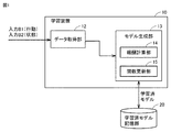
- FIG. 3 is a configuration diagram of a learning device 10 relating to a tool chain for developing a programmable logic device according to the first embodiment. It is a flowchart about the learning process of the learning apparatus 10 in Embodiment 1.
- FIG. FIG. 3 is a configuration diagram of an inference device 30 relating to a tool chain for developing a programmable logic device according to the first embodiment. It is a flowchart which shows the inference procedure of the parameter for iterative synthesis by the inference apparatus 30 in Embodiment 1.
- FIG. It is a figure which shows the structure of the learning apparatus 10A about the tool chain for development of the programmable logic device in Embodiment 2.
- FIG. It is a flowchart about the learning process of the learning apparatus 10A in Embodiment 2.
- FIG. It is a figure which shows the structure of the inference apparatus 30A which concerns on the tool chain for development of the programmable logic device in Embodiment 2.
- FIG. It is a flowchart which shows the inference procedure of the success probability of the arrangement and wiring of the inference apparatus 30A in Embodiment 2.
- FIG. 1 is a configuration diagram of a learning device 10 relating to a tool chain for developing a programmable logic device according to the first embodiment.
- the learning device 10 includes a data acquisition unit 12 and a model generation unit 13.
- the data acquisition unit 12 acquires the target clock frequency, the iterated synthesis parameter, the resource usage rate data for each technology, and the timing slack information at the time of technology mapping as learning data.
- the target clock frequency is the target clock frequency at which the programmable logic device is actually operated.
- Iterative synthesis means trying multiple placements and routings to achieve the target clock frequency after placement and routing.
- the target clock frequency or a clock frequency higher than the target clock frequency is set as the center frequency X [MHz], and a range of the threshold ⁇ [MHz] is set on the lower side and the higher side of the frequency, that is, (X).
- the range from ⁇ ) [MHz] to (X + ⁇ ) [MHz] is set, and the trial of placement and routing is repeated while changing the range by the step value ⁇ [MHz].
- the number of repeated synthesis trials is (2 ⁇ / ⁇ + 1).
- the parameters for iterative synthesis refer to the above X, ⁇ , and ⁇ .
- the lower limit value (X- ⁇ ) is set to a value larger than the target clock frequency.
- the resource usage data for each technology indicates the ratio of the number of usage to the available number for each of the various computational resources in the program logic device.
- the resource usage data for each technology is, for example, the usage rate of the ALU (arithmetic logic unit) of LE (Logic Element) or PE (Processing Element), the usage rate of the multiplexer, and the adder as a result of the technology mapping of the programmable logic device. Includes usage of the subtractor, usage of the arithmetic shifter, and so on.
- the model generation unit 13 uses the learning data including the target clock frequency acquired by the data acquisition unit 12, the parameters for iterative synthesis, the resource utilization data for each technology, and the timing slack information at the time of technology mapping, to be a programmable logic device. Learned to infer the parameters for iterative synthesis given to the development toolchain of programmable logic devices for successful placement and routing from resource utilization data for each technology in the development toolchain and timing slack information during technology mapping. Generate a model.
- the parameters for iterative synthesis are the clock center frequency X [MHz] for performing the above-mentioned iterative synthesis, the threshold value ⁇ [MHz] for determining the frequency range on the low side and the high side of the frequency, and the change within the frequency range. It is a step value ⁇ [MHz] for repeating the trial of placement and routing while making it.
- the "parameters for iterative synthesis for successful placement and routing" are the central clock frequency at which the circuit after placement and routing can achieve the desired signal processing performance, and the probability that each placement and routing result will be successful during execution of iterative synthesis. Is a combination of the threshold value ⁇ [MHz] and the step value ⁇ [MHz] so as to satisfy the condition that is the highest and the number of trials of placement and routing is the smallest.
- the threshold ⁇ [MHz] and the step value The combination of ⁇ [MHz] is determined.
- the maximum number of compute resources that can be used is not exceeded, the interconnect resources used do not exceed the maximum number of interconnect resources that can be used on the programmable logic device, and the signal propagation delay time between FFs (Flip Flops) is not exceeded. It is shown that the largest value among them does not exceed the cycle time determined by the target clock frequency.
- a known algorithm such as supervised learning, unsupervised learning, or reinforcement learning can be used.
- reinforcement learning an agent (behavior) in a certain environment observes the current state (environmental parameters) and decides the action to be taken. The environment changes dynamically depending on the behavior of the agent, and the agent is rewarded according to the change in the environment. The agent repeats this process and learns the action policy that gives the most reward through a series of actions.
- Q-learning or TD learning Temporal Difference Learning
- the general update formula of the action value function Q (s, a) is expressed by the formula (1).
- st represents the state of the environment at time t. at represents the action at time t.
- the state changes to st + 1 depending on the action at.
- rt + 1 represents the reward received by the change of the state.
- ⁇ represents the discount rate.
- ⁇ represents the learning coefficient.
- the range is 0 ⁇ ⁇ 1 and 0 ⁇ ⁇ 1.
- the parameter for iterative synthesis is behavior at.
- the resource usage data for each technology and the timing slack information at the time of technology mapping are in the state st.
- Q-learning the best action at in the state st at time t is learned.
- the action value Q of the action a having the highest Q value at time t + 1 is larger than the action value Q of the action a executed at time t, the action value Q is increased. However, in the opposite case, the action value Q is reduced. In other words, the action value function Q (s, a) is updated so that the action value Q of the action a at time t approaches the best action value at time t + 1. As a result, the best behavioral value in a certain environment is sequentially propagated to the behavioral value in the previous environment.
- the model generation unit 13 includes a reward calculation unit 14 and a function update unit 15.
- the reward calculation unit 14 calculates the reward based on the target clock frequency, the parameters for iterative synthesis, the resource utilization data for each technology, and the timing slack information at the time of technology mapping.
- the reward calculation unit 14 calculates the reward r based on the result of the placement and routing. For example, the reward calculation unit 14 increases the reward r (for example, gives a reward of "1") when the placement and routing is successful, and decreases the reward r when the placement and routing fails (for example,). Give a reward of "-1".).
- the reward calculation unit 14 increases the reward in proportion to the margin (%) of the usage rate of LE or PE in the programmable logic device when the placement and routing are successful, or the programmable logic device.
- the reward is increased in proportion to the margin (%) of the interconnect resource in the programmable logic device, or the cycle time in the largest signal propagation delay time (critical path) between FFs (Flip Flop) in the programmable logic device.
- the reward calculation unit 14 may increase the reward by combining a plurality of elements among the elements for increasing these three rewards (margin of arithmetic resource, margin of interconnect resource, timing margin of critical path). Also, if necessary, each element may be multiplied by a weighting factor to increase the reward.
- the reward calculation unit 14 reduces the reward in proportion to the overflow degree of LE or PE in the programmable logic device, or reduces the reward in proportion to the overflow degree of the interconnect resource in the programmable logic device. If none of the resources are overflowing, the degree of timing violation (Negative Slack value) for the cycle time in the largest signal propagation delay time (critical path) between FFs (Flip Flops) in the programmable device. ) Or reduce the reward in proportion to the degree of all timing violations (Total Negative Slack value).
- the reward calculation unit 14 may reduce the reward by combining a plurality of elements among the elements for reducing these three rewards (degree of overflow of arithmetic resources, degree of overflow of interconnect resources, degree of timing violation), and is also necessary. Depending on the situation, each element may be multiplied by a weighting factor to reduce the reward.
- the function update unit 15 updates the function for determining the iterated synthesis parameter for successful placement and routing according to the reward calculated by the reward calculation unit 14, and outputs the function to the trained model storage unit 20.
- the function update unit 15 uses the action value function Q (st, at) represented by the equation (1) as a function for calculating parameters for iterative synthesis for successful placement and routing. ..
- the trained model storage unit 20 stores the action value function Q (st, at) updated by the function update unit 15, that is, the trained model.
- FIG. 2 is a flowchart relating to the learning process of the learning device 10 according to the first embodiment.
- step S101 the data acquisition unit 12 acquires the target clock frequency, the iterated synthesis parameter, the resource usage rate data for each technology, and the timing slack information at the time of technology mapping as learning data.
- step S102 the model generation unit 13 calculates the reward based on the target clock frequency, the parameter for iterative synthesis, the resource utilization data for each technology, and the timing slack information at the time of technology mapping. Specifically, the reward calculation unit 14 acquires the target clock frequency, the parameter for iterated synthesis, the resource utilization data for each technology, and the timing slack information at the time of technology mapping, and increases the reward based on the result of the placement and routing. Decide whether to let or reduce. When the reward calculation unit 14 determines that the reward is to be increased, the process proceeds to step S103. When the reward calculation unit 14 determines that the reward is to be reduced, the process proceeds to step S104.
- step S103 the reward calculation unit 14 increases the reward.
- step S104 the reward calculation unit 14 reduces the reward.
- step S105 the function update unit 15 creates an action value function Q (st, at) represented by the equation (1) stored in the trained model storage unit 20 based on the reward calculated by the reward calculation unit 14. Update.
- the learning device 10 repeatedly executes the above steps S101 to S105, and stores the generated action value function Q (st, at) as a learned model.
- the learning device 10 stores the trained model in the trained model storage unit 20 provided outside the learning device 10, but the trained model storage unit 20 is stored inside the learning device 10. You may be prepared for.
- FIG. 3 is a configuration diagram of an inference device 30 relating to a tool chain for developing a programmable logic device according to the first embodiment.
- the inference device 30 includes a data acquisition unit 31 and an inference unit 32.
- the data acquisition unit 31 acquires resource usage data for each technology and timing slack information at the time of technology mapping.
- the inference unit 32 develops a programmable logic device for successful placement and routing from the trained model storage unit 20 from the resource utilization data for each technology of the tool chain for developing the programmable logic device and the timing slack information at the time of technology mapping. Read the trained model for inferring the parameters for iterative synthesis given to the toolchain.
- the inference unit 32 infers the parameters for iterative synthesis for successful placement and routing by using the data acquired by the data acquisition unit 31 and the trained model. That is, the inference unit 32 inputs the resource usage rate data for each technology acquired by the data acquisition unit 31 and the timing slack information at the time of technology mapping into the trained model, so that the resource usage rate data for each technology and the time of technology mapping are performed. It is possible to infer parameters for iterative synthesis for successful placement and routing suitable for the timing slack information of.
- the inference unit 32 reads the action value function Q (st, at) from the trained model storage unit 20 as a trained model.
- the inference unit 32 sets parameters for iterative synthesis (behavior at) based on the action value function Q (s, a) with respect to the resource utilization data for each technology and the timing slack information (state st) at the time of technology mapping. obtain.
- the iterative synthesis parameter included in this action at is the iterative synthesis parameter for successful placement and routing.
- the parameters for iterative synthesis for successful placement and routing are output using the trained model learned in the model generation unit 13 of the tool chain for developing a programmable logic device.
- a trained model may be obtained from the development tool chain of the programmable logic device, and parameters for iterative synthesis for successful placement and routing may be output based on the trained model.
- FIG. 4 is a flowchart showing the inference procedure of the parameters for iterative synthesis by the inference device 30 in the first embodiment.
- step S201 the data acquisition unit 31 acquires resource usage data for each technology and timing slack information at the time of technology mapping.
- step S202 the inference unit 32 inputs the resource usage rate data for each technology and the timing slack information at the time of technology mapping into the trained model stored in the trained model storage unit 20.
- step S203 the inference unit 32 obtains the parameters for iterative synthesis for successful placement and routing from the trained model.
- the inference unit 32 outputs the parameters for iterative synthesis for successful placement and routing to the tool chain for developing the programmable logic device.
- step S204 the tool chain for developing the programmable logic device uses the output parameters for iterative synthesis for successful placement and routing and the circuit configuration information by technology mapping, and the actual PE (Processing Element) on the programmable device. ), LE (Logic Element), SRAM (Static Random Access Memory), and the trial of placement and routing using interconnect resources are repeated, that is, iterative synthesis is performed.
- the composition constraint of the iterative synthesis is a parameter for iterative synthesis for succeeding the placement and routing output by step S203.
- reinforcement learning is applied to the learning algorithm used by the inference unit, but the present invention is not limited to this.
- learning algorithm in addition to reinforcement learning, supervised learning, unsupervised learning, semi-supervised learning, and the like can also be applied.
- deep learning for learning the extraction of the feature amount itself can also be used.
- machine learning may be performed according to other known methods such as neural networks, genetic programming, functional logic programming, or support vector machines.
- the learning device 10 and the inference device 30 may be connected to, for example, a tool chain for developing a programmable logic device via a network, and may be devices separate from the tool chain for developing the programmable logic device. Further, the learning device 10 and the inference device 30 may be built in a tool chain for developing a programmable logic device. Further, the learning device 10 and the inference device 30 may exist on the cloud server.
- the model generation unit 13 may learn the parameters for iterative synthesis for successful placement and routing by using the learning data acquired from the development tool chain of a plurality of programmable logic devices.
- the model generation unit 13 may acquire learning data from a tool chain for developing a plurality of programmable logic devices used in the same place, or a plurality of programmable logic devices operating independently in different places. You may get the learning data from the development toolchain of. It is also possible to add or remove a toolchain for developing a programmable logic device that collects learning data from the target on the way. Furthermore, a learning device that has learned parameters for iterative synthesis for successful placement and routing for one programmable logic device development toolchain is applied to another programmable logic device development toolchain. The parameters for iterative synthesis for successful placement and routing may be relearned and updated with respect to the toolchain for developing programmable logic devices.
- inference by artificial intelligence is performed in the process of repeatedly executing the placement and routing using the development tool chain of the programmable device and finding the clock and timing constraint conditions for successful placement and routing.
- the clock center frequency and frequency range obtained from the results are used.
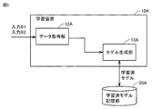
- FIG. 5 is a diagram showing a configuration of a learning device 10A relating to a tool chain for developing a programmable logic device according to a second embodiment.
- the learning device 10A includes a data acquisition unit 12A and a model generation unit 13A.
- the data acquisition unit 12A acquires the clock frequency, the iterated synthesis parameter, the resource usage rate data for each technology, and the timing slack information at the time of technology mapping as learning data.
- the model generation unit 13A is a learning data created based on a combination of the clock frequency output from the data acquisition unit 12A, the parameters for iterative synthesis, the resource usage rate data for each technology, and the timing slack information at the time of technology mapping. Learn the success rate of placement and routing based on. That is, a trained model that infers the success probability of placement and routing from the clock frequency of the toolchain for developing programmable logic devices, the parameters for iterated synthesis, the resource utilization data for each technology, and the timing slack information at the time of technology mapping is generated. ..
- the learning data is data in which the clock frequency, the parameters for iterative synthesis, the resource utilization data for each technology, and the timing slack information at the time of technology mapping are associated with each other.
- the trained model is the clock frequency at the time of successful placement and routing, parameters for iterative synthesis, resource utilization data for each technology, and timing slack during technology mapping. It is configured as a model for classifying (clustering) information, clock frequency when placement and routing fails, parameters for iterative synthesis, resource utilization data for each technology, and timing slack information at the time of technology mapping.
- Unsupervised learning is a method of learning the features of the learning data by giving the learning data that does not include the result (label) to the learning device.
- the model generation unit 13A learns the success probability of placement and routing by so-called unsupervised learning according to, for example, a grouping method based on the K-means method.
- the K-means method is a non-hierarchical clustering algorithm, which is a method of classifying a given number of clusters into k using the average of clusters.
- the K-means method is processed in the following flow. First, a cluster is randomly assigned to each data xi. Next, the center Vj of each cluster is calculated based on the allocated data. Then, the distance between each xi and each Vj is obtained, and xi is reassigned to the nearest central cluster. Then, when the allocation of all xi clusters does not change in the above process, or when the amount of change falls below a predetermined threshold value, it is determined that the process has converged and the process ends.
- the learning data created based on the combination of the clock frequency acquired by the data acquisition unit 12A, the parameters for iterative synthesis, the resource utilization data for each technology, and the timing slack information at the time of technology mapping. Learn the success probability of placement and routing by unsupervised learning.
- the model generation unit 13A generates and outputs a trained model by executing the above learning.
- the trained model storage unit 20A stores the trained model output from the model generation unit 13A.
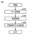
- FIG. 6 is a flowchart relating to the learning process of the learning device 10A according to the second embodiment.
- step S301 the data acquisition unit 12A acquires the clock frequency, the iterated synthesis parameter, the resource usage rate data for each technology, and the timing slack information at the time of technology mapping. It was assumed that the clock frequency, parameters for iterative synthesis, resource utilization data for each technology, and timing slack information at the time of technology mapping were acquired at the same time, but the clock frequency, parameters for iterative synthesis, resource utilization data for each technology, and It suffices if the timing slack information at the time of technology mapping can be input in association with each other. good.
- step S302 the model generation unit 13A is created based on the combination of the clock frequency acquired by the data acquisition unit 12A, the parameters for iterative synthesis, the resource utilization data for each technology, and the timing slack information at the time of technology mapping. According to the training data, the success probability of placement and routing is learned by so-called unsupervised learning, and a trained model is generated.
- step S303 the trained model storage unit 20A stores the trained model generated by the model generation unit 13A.
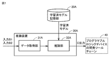
- FIG. 7 is a diagram showing a configuration of an inference device 30A relating to a tool chain for developing a programmable logic device according to the second embodiment.
- the inference device 30A includes a data acquisition unit 31A and an inference unit 32A.
- the data acquisition unit 31A acquires clock frequency, iterated synthesis parameters, resource usage data for each technology, and timing slack information at the time of technology mapping.
- the inference unit 32A infers the success probability of the placement and routing obtained by using the learned model stored in the learned model storage unit 20A. That is, the inference unit 32A inputs the clock frequency acquired by the data acquisition unit 31A, the parameter for iterative synthesis, the resource utilization data for each technology, and the timing slack information at the time of technology mapping into the trained model, thereby inputting the clock frequency. , Parameters for iterative synthesis, resource utilization data for each technology, and timing slack information at the time of technology mapping can be inferred to which cluster, and the inference result can be output as the success probability of placement and routing.
- the inference unit 32A uses the clock frequency input to the trained model, parameters for iterative synthesis, resource utilization data for each technology, and timing slack during technology mapping. Determine if the information belongs to a cluster that indicates successful placement and routing or a cluster that indicates failure in placement and routing. Then, if it belongs to a cluster indicating the success of the placement and routing, the inference unit 32A infers that the placement and routing is successful. On the other hand, if it belongs to a cluster indicating a placement and routing failure, the inference unit infers that the placement and routing fails.
- the inference unit 32A inputs the clock frequency acquired by the data acquisition unit 31A, the parameter for iterative synthesis, the resource utilization data for each technology, and the timing slack information at the time of technology mapping into the trained model, thereby inputting the clock frequency.
- Parameters for iterative synthesis, resource utilization data for each technology, and timing slack information at the time of technology mapping may be inferred and output to the probability that they belong to the cluster indicating the success of placement and routing. For example, the smaller the distance between the clock frequency entered in the trained model, the parameters for iterative synthesis, the resource utilization data for each technology, and the timing slack information during technology mapping, and the center of gravity of the cluster indicating the success of the placement and routing. , The probability of belonging to a cluster indicating the success of placement and routing may be increased.
- the model generation unit 13A uses the soft clustering method instead of the K-means method to generate a model that generates the probability of belonging to the cluster indicating the success of the placement and routing, and the inference unit 32A uses the soft clustering method. Then, the probability of belonging to the cluster indicating the success of the placement and routing may be inferred from the generated model.
- the success probability of placement and routing is output using the trained model learned in the model generation part of the tool chain for developing a programmable logic device, but it is a tool for developing other programmable logic devices.
- a trained model may be acquired from the outside such as a chain, and the success probability of placement and routing may be output based on this trained model.
- the inference unit 32A determines the success probability of the placement and routing obtained based on the clock frequency, the parameter for iterated synthesis, the resource utilization data for each technology, and the timing slack information at the time of technology mapping of the programmable logic device.
- FIG. 8 is a flowchart showing the inference procedure of the success probability of the placement and wiring of the inference device 30A in the second embodiment.
- step S401 the data acquisition unit 31A acquires the clock frequency, the iterated synthesis parameter, the resource usage rate data for each technology, and the timing slack information at the time of technology mapping.
- step S402 the inference unit 32A inputs the clock frequency, the parameter for iterative synthesis, the resource utilization data for each technology, and the timing slack information at the time of technology mapping into the trained model stored in the trained model storage unit 20A. , Obtain the success probability of placement and routing.
- step S403 the inference unit 32A outputs the success probability of the placement and routing obtained by the trained model to the tool chain for developing the programmable logic device.
- step S404 the tool chain for developing the programmable logic device considers the success probability of the output placement and routing, and actually PE (Processing Element), LE (Logic Element), SRAM (Static Random Access) on the programmable device. Repeated trials of placement and routing using Memory) and interconnect resources, that is, iterative synthesis. As a result, the success probability of placement and wiring can be displayed on a display device such as a display.
- PE Processing Element
- LE Logic Element
- SRAM Static Random Access
- the present invention is not limited to this.
- the learning algorithm it is also possible to apply reinforcement learning, supervised learning, semi-supervised learning, or the like, in addition to unsupervised learning.
- deep learning which learns the extraction of the feature amount itself, can be used, and other known methods may be used.
- the learning device 10A and the inference device 30A are connected to, for example, a tool chain for developing a programmable logic device via a network, and are devices separate from the tool chain for developing the programmable logic device. May be good. Further, the learning device 10A and the inference device 30A may be built in a tool chain for developing a programmable logic device. Further, the learning device 10A and the inference device 30A may exist on the cloud server.
- the model generation unit 13A may learn the success probability of placement and routing according to the learning data created for the development tool chain of a plurality of programmable logic devices.
- the model generation unit 13A may acquire learning data from a tool chain for developing a plurality of programmable logic devices used in the same area, or may acquire learning data from a plurality of programmable logic devices that operate independently in different areas. You may learn the success probability of placement and routing by using the learning data collected from the development tool chain of. It is also possible to add or remove a toolchain for developing a programmable logic device that collects learning data from the target on the way.
- a learning device that has learned the success probability of placement and routing for a tool chain for developing a programmable logic device is applied to a tool chain for developing another programmable logic device, and is used for developing another programmable logic device.
- the success probability of placement and routing may be relearned and updated with respect to the tool chain.
- FIG. 9 is a diagram showing a hardware configuration of a learning device 10, 10A, an inference device 30, 30A, or a tool chain 40 for developing a programmable logic device.
- the learning device 10, 10A, the inference device 30, 30A, and the tool chain 40 for developing a programmable logic device can configure the corresponding operation with the hardware or software of the digital circuit.
- the functions of the learning devices 10, 10A, the inference devices 30, 30A, and the tool chain 40 for developing the programmable logic device are realized by using software, the learning devices 10, 10A, the inference devices 30, 30A, and the programmable logic
- the device development tool chain 40 includes, for example, a processor 51 connected by a bus 53 and a memory 52, as shown in FIG. 9, so that the processor 51 executes a program stored in the memory 52. Can be done.
- 10,10A learning device 12,12A data acquisition unit, 13,13A model generation unit, 14 reward calculation unit, 15 function update unit, 20,20A learned model storage unit, 31,31A data acquisition unit, 32,32A inference Department, 40 Programmable logic device development tool chain, 51 processor, 52 memory, 53 bus.
Landscapes
- Engineering & Computer Science (AREA)
- Computer Hardware Design (AREA)
- Physics & Mathematics (AREA)
- Theoretical Computer Science (AREA)
- Evolutionary Computation (AREA)
- Geometry (AREA)
- General Engineering & Computer Science (AREA)
- General Physics & Mathematics (AREA)
- Software Systems (AREA)
- Medical Informatics (AREA)
- Computer Vision & Pattern Recognition (AREA)
- Artificial Intelligence (AREA)
- Design And Manufacture Of Integrated Circuits (AREA)
- Management, Administration, Business Operations System, And Electronic Commerce (AREA)
Priority Applications (3)
| Application Number | Priority Date | Filing Date | Title |
|---|---|---|---|
| US17/920,848 US12380264B2 (en) | 2020-06-09 | 2021-06-01 | Learning apparatus, inference apparatus, and programmable logic device development toolchain |
| JP2022530483A JP7466643B2 (ja) | 2020-06-09 | 2021-06-01 | 学習装置、推論装置、学習方法、および推論方法 |
| CN202180039757.XA CN115699010A (zh) | 2020-06-09 | 2021-06-01 | 学习装置、推理装置以及可编程逻辑器件的开发用工具链 |
Applications Claiming Priority (2)
| Application Number | Priority Date | Filing Date | Title |
|---|---|---|---|
| JP2020100016 | 2020-06-09 | ||
| JP2020-100016 | 2020-06-09 |
Publications (1)
| Publication Number | Publication Date |
|---|---|
| WO2021251206A1 true WO2021251206A1 (ja) | 2021-12-16 |
Family
ID=78845684
Family Applications (1)
| Application Number | Title | Priority Date | Filing Date |
|---|---|---|---|
| PCT/JP2021/020784 Ceased WO2021251206A1 (ja) | 2020-06-09 | 2021-06-01 | 学習装置、推論装置、およびプログラマブルロジックデバイスの開発用ツールチェーン |
Country Status (4)
| Country | Link |
|---|---|
| US (1) | US12380264B2 (https=) |
| JP (1) | JP7466643B2 (https=) |
| CN (1) | CN115699010A (https=) |
| WO (1) | WO2021251206A1 (https=) |
Cited By (2)
| Publication number | Priority date | Publication date | Assignee | Title |
|---|---|---|---|---|
| CN114371970A (zh) * | 2022-01-10 | 2022-04-19 | 电子科技大学 | 一种基于图强化学习的fpga互联资源测试算法 |
| JP2025515970A (ja) * | 2022-06-13 | 2025-05-20 | 三菱電機株式会社 | 深層強化学習を用いたgan分散型rf電力増幅器自動化設計 |
Families Citing this family (1)
| Publication number | Priority date | Publication date | Assignee | Title |
|---|---|---|---|---|
| US12353809B2 (en) * | 2021-12-21 | 2025-07-08 | Synopsys, Inc. | Transformations for multicycle path prediction of clock signals |
Citations (3)
| Publication number | Priority date | Publication date | Assignee | Title |
|---|---|---|---|---|
| JP2007538474A (ja) * | 2004-05-19 | 2007-12-27 | アルテラ コーポレイション | 集積回路の性能を調整するための装置および方法 |
| US7500216B1 (en) * | 2007-02-07 | 2009-03-03 | Altera Corporation | Method and apparatus for performing physical synthesis hill-climbing on multi-processor machines |
| JP2020506491A (ja) * | 2017-01-08 | 2020-02-27 | アルファイクス コーポレイションAlphaics Corporation | 人工知能および強化学習によるシステムオンチップ(SoC)回路の設計システムおよび方法 |
Family Cites Families (9)
| Publication number | Priority date | Publication date | Assignee | Title |
|---|---|---|---|---|
| US8024675B1 (en) * | 2006-08-04 | 2011-09-20 | Tela Innovations, Inc. | Method and system for wafer topography-aware integrated circuit design analysis and optimization |
| US8365111B2 (en) * | 2008-02-29 | 2013-01-29 | Et International, Inc. | Data driven logic simulation |
| US8347243B2 (en) * | 2008-05-15 | 2013-01-01 | Universiteit Gent | Parameterized configuration for a programmable logic device |
| JP2016095606A (ja) * | 2014-11-13 | 2016-05-26 | 国立大学法人電気通信大学 | データ処理装置およびデータ処理方法、並びにプログラム |
| US9703920B2 (en) * | 2015-06-30 | 2017-07-11 | International Business Machines Corporation | Intra-run design decision process for circuit synthesis |
| CN105930609B (zh) * | 2016-05-04 | 2018-12-14 | 华中科技大学 | 一种用于相干解调的fpga时序优化方法 |
| EP3333735B1 (en) * | 2016-12-12 | 2021-07-07 | Fraunhofer-Gesellschaft zur Förderung der angewandten Forschung e.V. | Method and computer program for determining a placement of at least one circuit for a reconfigurable logic device |
| US10192016B2 (en) | 2017-01-17 | 2019-01-29 | Xilinx, Inc. | Neural network based physical synthesis for circuit designs |
| US10437954B1 (en) | 2017-06-30 | 2019-10-08 | Cadence Design Systems, Inc. | System and method for recommending integrated circuit placement and routing options |
-
2021
- 2021-06-01 WO PCT/JP2021/020784 patent/WO2021251206A1/ja not_active Ceased
- 2021-06-01 JP JP2022530483A patent/JP7466643B2/ja active Active
- 2021-06-01 CN CN202180039757.XA patent/CN115699010A/zh active Pending
- 2021-06-01 US US17/920,848 patent/US12380264B2/en active Active
Patent Citations (3)
| Publication number | Priority date | Publication date | Assignee | Title |
|---|---|---|---|---|
| JP2007538474A (ja) * | 2004-05-19 | 2007-12-27 | アルテラ コーポレイション | 集積回路の性能を調整するための装置および方法 |
| US7500216B1 (en) * | 2007-02-07 | 2009-03-03 | Altera Corporation | Method and apparatus for performing physical synthesis hill-climbing on multi-processor machines |
| JP2020506491A (ja) * | 2017-01-08 | 2020-02-27 | アルファイクス コーポレイションAlphaics Corporation | 人工知能および強化学習によるシステムオンチップ(SoC)回路の設計システムおよび方法 |
Cited By (3)
| Publication number | Priority date | Publication date | Assignee | Title |
|---|---|---|---|---|
| CN114371970A (zh) * | 2022-01-10 | 2022-04-19 | 电子科技大学 | 一种基于图强化学习的fpga互联资源测试算法 |
| JP2025515970A (ja) * | 2022-06-13 | 2025-05-20 | 三菱電機株式会社 | 深層強化学習を用いたgan分散型rf電力増幅器自動化設計 |
| JP7822521B2 (ja) | 2022-06-13 | 2026-03-02 | 三菱電機株式会社 | 深層強化学習を用いたgan分散型rf電力増幅器自動化設計 |
Also Published As
| Publication number | Publication date |
|---|---|
| JP7466643B2 (ja) | 2024-04-12 |
| CN115699010A (zh) | 2023-02-03 |
| US20230342530A1 (en) | 2023-10-26 |
| US12380264B2 (en) | 2025-08-05 |
| JPWO2021251206A1 (https=) | 2021-12-16 |
Similar Documents
| Publication | Publication Date | Title |
|---|---|---|
| JP6799197B2 (ja) | ニューラルネットワーク構築装置、情報処理装置、ニューラルネットワーク構築方法及びプログラム | |
| JP6605259B2 (ja) | ニューラルネットワーク構造拡張方法、次元縮小方法、及びその方法を用いた装置 | |
| Elgammal et al. | RLPlace: Using reinforcement learning and smart perturbations to optimize FPGA placement | |
| WO2021251206A1 (ja) | 学習装置、推論装置、およびプログラマブルロジックデバイスの開発用ツールチェーン | |
| CN115066694B (zh) | 计算图优化 | |
| Fadlullah et al. | Value iteration architecture based deep learning for intelligent routing exploiting heterogeneous computing platforms | |
| WO2020062165A1 (zh) | 一种强化学习模型的训练方法、节点、系统及存储介质 | |
| Muhsen et al. | Enhancing NoC-based MPSoC performance: a predictive approach with ANN and guaranteed convergence arithmetic optimization algorithm | |
| CN115062786B (zh) | 一种用于量子计算机的量子比特映射和量子门调度方法 | |
| Rada-Vilela et al. | Optimal computing budget allocation in particle swarm optimization | |
| Krithivasan et al. | Dynamic spike bundling for energy-efficient spiking neural networks | |
| TWI893495B (zh) | 逆向微影技術中光罩最佳化之機器學習 | |
| CN112016611B (zh) | 生成器网络和策略生成网络的训练方法、装置和电子设备 | |
| JP7582471B2 (ja) | シミュレーテッドアニーリング装置およびシミュレーテッドアニーリング方法 | |
| Al-Behadili et al. | Ant colony optimization algorithm for rule-based classification: Issues and potential solutions | |
| Ziegler et al. | Online and offline machine learning for industrial design flow tuning:(Invited-ICCAD special session paper) | |
| Al-Behadili et al. | Annealing strategy for an enhance rule pruning technique in ACO-based rule classification | |
| JP2023062490A (ja) | 学習プログラム、学習方法及び情報処理装置 | |
| Al-Hchaimi et al. | Reinforcement Guided Genetic Algorithm for Application Mapping in Network-on-Chip Architectures: Towards Transparent and Efficient MPSoC Scheduling | |
| CN116431421B (zh) | 神经网络生成方法及生成器、验证方法及系统、存储介质 | |
| Mitra et al. | Variable ordering for shared binary decision diagrams targeting node count and path length optimisation using particle swarm technique | |
| Cao et al. | A collaboration-based particle swarm optimizer for global optimization problems | |
| JP2021140493A (ja) | 情報処理装置、情報処理方法およびプログラム | |
| CN114399033B (zh) | 基于神经元指令编码的类脑计算系统和计算方法 | |
| CN112906745B (zh) | 基于边缘协同的诚信智能网络训练方法 |
Legal Events
| Date | Code | Title | Description |
|---|---|---|---|
| 121 | Ep: the epo has been informed by wipo that ep was designated in this application |
Ref document number: 21822795 Country of ref document: EP Kind code of ref document: A1 |
|
| ENP | Entry into the national phase |
Ref document number: 2022530483 Country of ref document: JP Kind code of ref document: A |
|
| NENP | Non-entry into the national phase |
Ref country code: DE |
|
| 122 | Ep: pct application non-entry in european phase |
Ref document number: 21822795 Country of ref document: EP Kind code of ref document: A1 |
|
| WWG | Wipo information: grant in national office |
Ref document number: 17920848 Country of ref document: US |