WO2021246441A1 - 光学フィルム、光学積層体および画像表示装置 - Google Patents
光学フィルム、光学積層体および画像表示装置 Download PDFInfo
- Publication number
- WO2021246441A1 WO2021246441A1 PCT/JP2021/020986 JP2021020986W WO2021246441A1 WO 2021246441 A1 WO2021246441 A1 WO 2021246441A1 JP 2021020986 W JP2021020986 W JP 2021020986W WO 2021246441 A1 WO2021246441 A1 WO 2021246441A1
- Authority
- WO
- WIPO (PCT)
- Prior art keywords
- group
- light absorption
- layer
- formula
- optical film
- Prior art date
- Legal status (The legal status is an assumption and is not a legal conclusion. Google has not performed a legal analysis and makes no representation as to the accuracy of the status listed.)
- Ceased
Links
Classifications
-
- C—CHEMISTRY; METALLURGY
- C09—DYES; PAINTS; POLISHES; NATURAL RESINS; ADHESIVES; COMPOSITIONS NOT OTHERWISE PROVIDED FOR; APPLICATIONS OF MATERIALS NOT OTHERWISE PROVIDED FOR
- C09K—MATERIALS FOR MISCELLANEOUS APPLICATIONS, NOT PROVIDED FOR ELSEWHERE
- C09K19/00—Liquid crystal materials
- C09K19/52—Liquid crystal materials characterised by components which are not liquid crystals, e.g. additives with special physical aspect: solvents, solid particles
- C09K19/60—Pleochroic dyes
- C09K19/601—Azoic
-
- C—CHEMISTRY; METALLURGY
- C09—DYES; PAINTS; POLISHES; NATURAL RESINS; ADHESIVES; COMPOSITIONS NOT OTHERWISE PROVIDED FOR; APPLICATIONS OF MATERIALS NOT OTHERWISE PROVIDED FOR
- C09K—MATERIALS FOR MISCELLANEOUS APPLICATIONS, NOT PROVIDED FOR ELSEWHERE
- C09K19/00—Liquid crystal materials
- C09K19/04—Liquid crystal materials characterised by the chemical structure of the liquid crystal components, e.g. by a specific unit
- C09K19/38—Polymers
- C09K19/3833—Polymers with mesogenic groups in the side chain
- C09K19/3842—Polyvinyl derivatives
- C09K19/3852—Poly(meth)acrylate derivatives
-
- C—CHEMISTRY; METALLURGY
- C09—DYES; PAINTS; POLISHES; NATURAL RESINS; ADHESIVES; COMPOSITIONS NOT OTHERWISE PROVIDED FOR; APPLICATIONS OF MATERIALS NOT OTHERWISE PROVIDED FOR
- C09K—MATERIALS FOR MISCELLANEOUS APPLICATIONS, NOT PROVIDED FOR ELSEWHERE
- C09K19/00—Liquid crystal materials
- C09K19/52—Liquid crystal materials characterised by components which are not liquid crystals, e.g. additives with special physical aspect: solvents, solid particles
- C09K19/60—Pleochroic dyes
-
- C—CHEMISTRY; METALLURGY
- C09—DYES; PAINTS; POLISHES; NATURAL RESINS; ADHESIVES; COMPOSITIONS NOT OTHERWISE PROVIDED FOR; APPLICATIONS OF MATERIALS NOT OTHERWISE PROVIDED FOR
- C09K—MATERIALS FOR MISCELLANEOUS APPLICATIONS, NOT PROVIDED FOR ELSEWHERE
- C09K19/00—Liquid crystal materials
- C09K19/52—Liquid crystal materials characterised by components which are not liquid crystals, e.g. additives with special physical aspect: solvents, solid particles
- C09K19/60—Pleochroic dyes
- C09K19/603—Anthroquinonic
-
- G—PHYSICS
- G02—OPTICS
- G02B—OPTICAL ELEMENTS, SYSTEMS OR APPARATUS
- G02B5/00—Optical elements other than lenses
- G02B5/003—Light absorbing elements
-
- G—PHYSICS
- G02—OPTICS
- G02B—OPTICAL ELEMENTS, SYSTEMS OR APPARATUS
- G02B5/00—Optical elements other than lenses
- G02B5/20—Filters
- G02B5/208—Filters for use with infrared or ultraviolet radiation, e.g. for separating visible light from infrared and/or ultraviolet radiation
-
- G—PHYSICS
- G02—OPTICS
- G02B—OPTICAL ELEMENTS, SYSTEMS OR APPARATUS
- G02B5/00—Optical elements other than lenses
- G02B5/20—Filters
- G02B5/22—Absorbing filters
- G02B5/223—Absorbing filters containing organic substances, e.g. dyes, inks or pigments
-
- G—PHYSICS
- G02—OPTICS
- G02B—OPTICAL ELEMENTS, SYSTEMS OR APPARATUS
- G02B5/00—Optical elements other than lenses
- G02B5/20—Filters
- G02B5/22—Absorbing filters
- G02B5/24—Liquid filters
-
- G—PHYSICS
- G02—OPTICS
- G02B—OPTICAL ELEMENTS, SYSTEMS OR APPARATUS
- G02B5/00—Optical elements other than lenses
- G02B5/30—Polarising elements
-
- G—PHYSICS
- G02—OPTICS
- G02B—OPTICAL ELEMENTS, SYSTEMS OR APPARATUS
- G02B5/00—Optical elements other than lenses
- G02B5/30—Polarising elements
- G02B5/3016—Polarising elements involving passive liquid crystal elements
-
- G—PHYSICS
- G02—OPTICS
- G02F—OPTICAL DEVICES OR ARRANGEMENTS FOR THE CONTROL OF LIGHT BY MODIFICATION OF THE OPTICAL PROPERTIES OF THE MEDIA OF THE ELEMENTS INVOLVED THEREIN; NON-LINEAR OPTICS; FREQUENCY-CHANGING OF LIGHT; OPTICAL LOGIC ELEMENTS; OPTICAL ANALOGUE/DIGITAL CONVERTERS
- G02F1/00—Devices or arrangements for the control of the intensity, colour, phase, polarisation or direction of light arriving from an independent light source, e.g. switching, gating or modulating; Non-linear optics
- G02F1/01—Devices or arrangements for the control of the intensity, colour, phase, polarisation or direction of light arriving from an independent light source, e.g. switching, gating or modulating; Non-linear optics for the control of the intensity, phase, polarisation or colour
- G02F1/13—Devices or arrangements for the control of the intensity, colour, phase, polarisation or direction of light arriving from an independent light source, e.g. switching, gating or modulating; Non-linear optics for the control of the intensity, phase, polarisation or colour based on liquid crystals, e.g. single liquid crystal display cells
- G02F1/133—Constructional arrangements; Operation of liquid crystal cells; Circuit arrangements
- G02F1/1333—Constructional arrangements; Manufacturing methods
- G02F1/1335—Structural association of cells with optical devices, e.g. polarisers or reflectors
- G02F1/133509—Filters, e.g. light shielding masks
- G02F1/133514—Colour filters
-
- G—PHYSICS
- G02—OPTICS
- G02F—OPTICAL DEVICES OR ARRANGEMENTS FOR THE CONTROL OF LIGHT BY MODIFICATION OF THE OPTICAL PROPERTIES OF THE MEDIA OF THE ELEMENTS INVOLVED THEREIN; NON-LINEAR OPTICS; FREQUENCY-CHANGING OF LIGHT; OPTICAL LOGIC ELEMENTS; OPTICAL ANALOGUE/DIGITAL CONVERTERS
- G02F1/00—Devices or arrangements for the control of the intensity, colour, phase, polarisation or direction of light arriving from an independent light source, e.g. switching, gating or modulating; Non-linear optics
- G02F1/01—Devices or arrangements for the control of the intensity, colour, phase, polarisation or direction of light arriving from an independent light source, e.g. switching, gating or modulating; Non-linear optics for the control of the intensity, phase, polarisation or colour
- G02F1/13—Devices or arrangements for the control of the intensity, colour, phase, polarisation or direction of light arriving from an independent light source, e.g. switching, gating or modulating; Non-linear optics for the control of the intensity, phase, polarisation or colour based on liquid crystals, e.g. single liquid crystal display cells
- G02F1/133—Constructional arrangements; Operation of liquid crystal cells; Circuit arrangements
- G02F1/1333—Constructional arrangements; Manufacturing methods
- G02F1/1335—Structural association of cells with optical devices, e.g. polarisers or reflectors
- G02F1/133528—Polarisers
- G02F1/133533—Colour selective polarisers
-
- G—PHYSICS
- G09—EDUCATION; CRYPTOGRAPHY; DISPLAY; ADVERTISING; SEALS
- G09F—DISPLAYING; ADVERTISING; SIGNS; LABELS OR NAME-PLATES; SEALS
- G09F9/00—Indicating arrangements for variable information in which the information is built-up on a support by selection or combination of individual elements
-
- H—ELECTRICITY
- H05—ELECTRIC TECHNIQUES NOT OTHERWISE PROVIDED FOR
- H05B—ELECTRIC HEATING; ELECTRIC LIGHT SOURCES NOT OTHERWISE PROVIDED FOR; CIRCUIT ARRANGEMENTS FOR ELECTRIC LIGHT SOURCES, IN GENERAL
- H05B33/00—Electroluminescent light sources
- H05B33/02—Details
-
- C—CHEMISTRY; METALLURGY
- C09—DYES; PAINTS; POLISHES; NATURAL RESINS; ADHESIVES; COMPOSITIONS NOT OTHERWISE PROVIDED FOR; APPLICATIONS OF MATERIALS NOT OTHERWISE PROVIDED FOR
- C09K—MATERIALS FOR MISCELLANEOUS APPLICATIONS, NOT PROVIDED FOR ELSEWHERE
- C09K19/00—Liquid crystal materials
- C09K19/04—Liquid crystal materials characterised by the chemical structure of the liquid crystal components, e.g. by a specific unit
- C09K2019/0444—Liquid crystal materials characterised by the chemical structure of the liquid crystal components, e.g. by a specific unit characterized by a linking chain between rings or ring systems, a bridging chain between extensive mesogenic moieties or an end chain group
- C09K2019/0448—Liquid crystal materials characterised by the chemical structure of the liquid crystal components, e.g. by a specific unit characterized by a linking chain between rings or ring systems, a bridging chain between extensive mesogenic moieties or an end chain group the end chain group being a polymerizable end group, e.g. -Sp-P or acrylate
-
- G—PHYSICS
- G02—OPTICS
- G02F—OPTICAL DEVICES OR ARRANGEMENTS FOR THE CONTROL OF LIGHT BY MODIFICATION OF THE OPTICAL PROPERTIES OF THE MEDIA OF THE ELEMENTS INVOLVED THEREIN; NON-LINEAR OPTICS; FREQUENCY-CHANGING OF LIGHT; OPTICAL LOGIC ELEMENTS; OPTICAL ANALOGUE/DIGITAL CONVERTERS
- G02F1/00—Devices or arrangements for the control of the intensity, colour, phase, polarisation or direction of light arriving from an independent light source, e.g. switching, gating or modulating; Non-linear optics
- G02F1/01—Devices or arrangements for the control of the intensity, colour, phase, polarisation or direction of light arriving from an independent light source, e.g. switching, gating or modulating; Non-linear optics for the control of the intensity, phase, polarisation or colour
- G02F1/13—Devices or arrangements for the control of the intensity, colour, phase, polarisation or direction of light arriving from an independent light source, e.g. switching, gating or modulating; Non-linear optics for the control of the intensity, phase, polarisation or colour based on liquid crystals, e.g. single liquid crystal display cells
- G02F1/133—Constructional arrangements; Operation of liquid crystal cells; Circuit arrangements
- G02F1/1333—Constructional arrangements; Manufacturing methods
- G02F1/1335—Structural association of cells with optical devices, e.g. polarisers or reflectors
- G02F1/133509—Filters, e.g. light shielding masks
Definitions
- the present invention relates to an optical film, an optical laminate, and an image display device.
- Patent Document 1 proposes a polarizing element relating to a viewing angle control system using a film containing a dichroic substance and having an angle formed by an absorption axis and a normal of the film surface of 0 ° to 45 °.
- the present inventors have studied an optical film having a light absorption anisotropic layer containing a dichroic substance, and found that the optical film can be thinned, so that it is excellent in processing suitability. Since the orientation of the dichroic substance in the visible region is not uniform, the color of the optical film when viewed from the center axis of the transmittance of the light absorption anisotropic layer and the direction tilted from the center axis of the transmittance. It was clarified that it is difficult to control the color tones when viewed from the above.
- the present invention provides an optical film capable of neutralizing both the tint when viewed from the central axis of transmittance and the tint when viewed from the direction inclined from the central axis of transmittance.
- An object of the present invention is to provide an optical laminate and an image display device used.
- an optical film having a predetermined light absorption anisotropic layer and a color adjustment layer having at least one organic dye compound has a transmittance central axis.
- both the tint when viewed from the direction and the tint when viewed from the direction inclined from the central axis of transmittance can be neutral, and have completed the present invention.
- [1] It has a light absorption anisotropic layer having an angle ⁇ formed by the central axis of transmittance and the normal direction of the layer surface of 0 to 45 °, and a color adjustment layer containing at least one organic dye compound.
- Optical film [2] The optical film according to [1], wherein the light absorption anisotropic layer contains a liquid crystal compound and at least one dichroic dye compound.
- an optical film capable of neutralizing both the tint when viewed from the central axis of transmittance and the tint when viewed from the direction inclined from the central axis of transmittance, and the like. It is possible to provide an optical laminate and an image display device using the above.
- the numerical range represented by using "-" means a range including the numerical values before and after "-" as the lower limit value and the upper limit value.
- parallel and orthogonal do not mean parallel and orthogonal in the strict sense, but mean a range of parallel ⁇ 5 ° and a range of orthogonal ⁇ 5 °, respectively.
- visible light means an electromagnetic wave having a wavelength of 380 to 800 nm, unless otherwise specified.
- room temperature means 20 to 28 ° C. unless otherwise specified.
- liquid crystal composition and the liquid crystal compound include those which no longer show liquid crystal property due to curing or the like as a concept.
- each component the substance corresponding to each component may be used alone or in combination of two or more.
- the content of the component means the total content of the substances used in combination unless otherwise specified.
- (meth) acrylate is a notation representing "acrylate” or “methacrylate”
- (meth) acrylic is a notation representing "acrylic” or “methacrylic”
- (meth) acrylic is used.
- “Acryloyl” is a notation representing "acryloyl” or "methacrylic acid”.
- the substituent W in the present specification will be described.
- the substituent W is, for example, an alkyl group (preferably an alkyl group having 1 to 20 carbon atoms, more preferably 1 to 12 carbon atoms, particularly preferably 1 to 8 carbon atoms, and for example, a methyl group or an ethyl group. Isopropyl group, tert-butyl group, n-octyl group, n-decyl group, n-hexadecyl group, cyclopropyl group, cyclopentyl group, cyclohexyl group and the like), alkenyl group (preferably 2 to 20 carbon atoms).
- a group preferably an alkynyl group having 2 to 20 carbon atoms, more preferably 2 to 12 carbon atoms, particularly preferably 2 to 8 carbon atoms, and examples thereof include a propargyl group and a 3-pentynyl group).
- An aryl group (preferably an aryl group having 6 to 30 carbon atoms, more preferably 6 to 20 carbon atoms, particularly preferably 6 to 12 carbon atoms, for example, a phenyl group, a 2,6-diethylphenyl group, 3,5 -Ditrifluoromethylphenyl group, styryl group, naphthyl group, biphenyl group and the like), substituted or unsubstituted amino group (preferably 0 to 20 carbon atoms, more preferably 0 to 10 carbon atoms, particularly preferable.
- Is an amino group having 0 to 6 carbon atoms examples thereof include an unsubstituted amino group, a methylamino group, a dimethylamino group, a diethylamino group, an anirino group and the like), and an alkoxy group (preferably 1 to 20 carbon atoms). , More preferably 1 to 15 carbon atoms, for example, methoxy group, ethoxy group, butoxy group and the like), oxycarbonyl group (preferably 2 to 20 carbon atoms, more preferably 2 to 15 carbon atoms).
- 10 particularly preferably 2 to 6 carbon atoms, for example, an acetylamino group, a benzoylamino group, etc.), an alkoxycarbonylamino group (preferably carbon).
- the number is 2 to 20, more preferably 2 to 10 carbon atoms, particularly preferably 2 to 6 carbon atoms, and examples thereof include a methoxycarbonylamino group and the like), and an aryloxycarbonylamino group (preferably 7 to 20 carbon atoms).
- the number is 1 to 10, particularly preferably 1 to 6, and examples thereof include a methanesulfonylamino group and a benzenesulfonylamino group), a sulfamoyl group (preferably 0 to 20, more preferably carbon).
- the number is 0 to 10, particularly preferably 0 to 6, and examples thereof include a sulfamoyl group, a methylsulfamoyl group, a dimethylsulfamoyl group, a phenylsulfamoyl group, and the like), and a carbamoyl group (preferably. Has 1 to 20 carbon atoms, more preferably 1 to 10 carbon atoms, particularly preferably 1 to 6 carbon atoms, and for example, an unsubstituted carbamoyl group, a methylcarbamoyl group, a diethylcarbamoyl group, a phenylcarbamoyl group and the like.
- An alkylthio group (preferably 1 to 20 carbon atoms, more preferably 1 to 10 carbon atoms, particularly preferably 1 to 6 carbon atoms, and examples thereof include a methylthio group and an ethylthio group).
- An arylthio group (preferably 6 to 20, more preferably 6 to 16, particularly preferably 6 to 12, such as a phenylthio group), a sulfonyl group (preferably 1 to 1 to carbon).
- Has 1 to 10 carbon atoms particularly preferably 1 to 6 carbon atoms, and examples thereof include a methanesulfinyl group and a benzenesulfinyl group, and a ureido group (preferably 1 to 20 carbon atoms, more preferably carbon atoms.
- the number is 1 to 10, particularly preferably 1 to 6 carbon atoms, and examples thereof include an unsubstituted ureido group, a methyl ureido group, a phenyl ureido group and the like), and a phosphate amide group (preferably 1 to 6 carbon atoms).
- ⁇ 20 more preferably 1 to 10 carbon atoms, particularly preferably 1 to 6 carbon atoms, and examples thereof include a diethyl phosphate amide group and a phenyl phosphate amide group.
- a heterocyclic group (preferably a heterocyclic group having 1 to 30 carbon atoms, more preferably 1 to 12 carbon atoms, for example, a heterocyclic group having a heteroatomic atom such as a nitrogen atom, an oxygen atom, a sulfur atom, etc.
- a heterocyclic group having a heteroatomic atom such as a nitrogen atom, an oxygen atom, a sulfur atom, etc.
- Cyril etc.
- a group preferably a silyl group having 3 to 40 carbon atoms, more preferably 3 to 30 carbon atoms, particularly preferably 3 to 24 carbon atoms, and examples thereof include a trimethylsilyl group and a triphenylsilyl group.
- wide-angle tint suppression refers to the state in which "the tint when viewed from the central axis of transmittance and the tint when viewed from the direction inclined from the central axis of transmittance are both neutral". It is also called “excellent in sex”.
- the optical film of the present invention contains a light absorption anisotropic layer having an angle ⁇ between the central axis of transmittance and the normal direction of the layer surface of 0 to 45 °, and a tint adjustment containing at least one organic dye compound. Has a layer.
- the mechanism by which the optical film of the present invention can both neutralize the color when viewed from the central axis of transmittance and the color when viewed from the direction inclined from the central axis of transmittance is not necessarily the mechanism. Although it is not clear, the present inventors speculate as follows.
- the color tone when viewed from the above two directions is not neutral, because the color tone due to the orientation of the substance contained in the light absorption anisotropic layer is generated. Is presumed to be the cause.
- the tint can be reduced by the tint adjusting layer containing at least one organic dye compound, and the tint when viewed from the two directions can be both neutral.
- the optical film of the present invention may have a transparent base film, an alignment film, a barrier layer, an adhesive layer, and an adhesive layer in addition to the light absorption anisotropic layer and the color tone adjusting layer.
- a transparent base film an alignment film
- a barrier layer an adhesive layer
- an adhesive layer an adhesive layer in addition to the light absorption anisotropic layer and the color tone adjusting layer.
- the light absorption anisotropic layer, the color adjustment layer, the transparent base film, the alignment film, and the barrier layer will be described in detail.
- the method for manufacturing the optical film will be described in detail below.
- the adhesive layer and the adhesive layer will be described in the method for manufacturing an optical film.
- the light absorption anisotropic layer of the optical film of the present invention has an angle between the central axis of transmittance and the normal direction of the layer surface of 0 ° to 45 °.
- the central axis of transmittance is the highest transmittance when the transmittance is measured by changing the inclination angle (extreme angle) and the inclination direction (azimuth angle) with respect to the normal direction of the surface of the light absorption anisotropic layer. It means the direction indicating the rate.
- AxoScan OPMF-1 manufactured by Optoscience is used to actually measure the Muller matrix at a wavelength of 550 nm.
- the azimuth angle at which the central axis of transmittance is tilted is first searched for, and then the surface including the normal direction of the light absorption anisotropic layer along the azimuth angle ( Within the plane including the central axis of transmittance and orthogonal to the layer surface), the polar angle, which is the angle of the surface of the light absorption anisotropic layer with respect to the normal direction, is changed from 0 to 90 ° in 5 ° increments, and the wavelength is 550 nm.
- the Muller matrix is actually measured and the transmittance of the light absorption anisotropic layer is derived. As a result, the direction with the highest transmittance is defined as the central axis of transmittance.
- the center of the viewing angle of the liquid crystal display device can be shifted not only from the front to the top, bottom, left and right, but also in the diagonal direction. can.
- the light absorption anisotropic layer preferably contains a liquid crystal compound and a dichroic substance.
- One example is a light absorption anisotropic layer in which at least one kind of organic dichroic dye is oriented perpendicularly to the in-plane.
- the light absorption anisotropic layer is preferably produced by using a composition for forming a light absorption anisotropic layer, which will be described later.
- the composition for forming a light absorption anisotropic layer preferably contains a liquid crystal compound and a dichroic substance. The composition for forming a light absorption anisotropic layer and the forming method using the composition will be described in detail later.
- the light absorption anisotropic layer of the optical film of the present invention preferably contains a liquid crystal compound.
- a liquid crystal compound when forming the light absorption anisotropic layer, it is possible to increase the degree of orientation of the dichroic substance in the light absorption anisotropic layer while suppressing the precipitation of the dichroic substance. can.
- the liquid crystal compound refers to a liquid crystal compound that does not exhibit dichroism with respect to at least visible light.
- the liquid crystal compound either a low-molecular-weight liquid crystal compound or a high-molecular-weight liquid crystal compound can be used, and it is preferable to use both in combination.
- the "low molecular weight liquid crystal compound” means a liquid crystal compound having no repeating unit in the chemical structure.
- the "polymer liquid crystal compound” means a liquid crystal compound having a repeating unit in the chemical structure.
- Examples of the low molecular weight liquid crystal compound include the liquid crystal compound described in JP-A-2013-228706.
- polymer liquid crystal compound examples include thermotropic liquid crystal polymers described in JP-A-2011-237513. Further, the polymer liquid crystal compound preferably has a repeating unit having a crosslinkable group at the terminal in that the strength (particularly, bending resistance) of the light absorption anisotropic film is excellent. Examples of the crosslinkable group include the polymerizable group described in paragraphs [0040] to [0050] of JP-A-2010-244038.
- an acryloyl group, a methacryloyl group, an epoxy group, an oxetanyl group, and a styryl group are preferable, and an acryloyl group and a methacryloyl group are more preferable, in terms of improving reactivity and synthetic suitability.
- the polymer liquid crystal compound When the light absorption anisotropic layer in the present invention contains a polymer liquid crystal compound, the polymer liquid crystal compound preferably forms a nematic liquid crystal phase.
- the temperature range indicating the nematic liquid crystal phase is preferably room temperature or higher and 450 ° C. or lower, and is preferably 50 to 400 ° C. in terms of handleability and / or manufacturing suitability.
- the content of the liquid crystal compound is preferably 25 to 2000 parts by mass, more preferably 100 to 1300 parts by mass, still more preferably 200 to 900 parts by mass, based on 100 parts by mass of the dichroic substance.
- the liquid crystal compound may be contained alone or in combination of two or more.
- the content of the liquid crystal compounds means the total content of the liquid crystal compounds.
- the liquid crystal compound has a repeating unit represented by the following formula (1L) (hereinafter, also referred to as “repeating unit (1L)”) in that the degree of orientation of the dichroic substance in the light absorption anisotropic layer is more excellent. It is preferably a polymer liquid crystal compound containing the compound.
- P1 represents the main chain of the repeating unit
- L1 represents a single bond or a divalent linking group
- SP1 represents a spacer group
- M1 represents a mesogen group
- T1 represents a terminal group. ..
- main chain of the repeating unit represented by P1 include groups represented by the following formulas (P1-A) to (P1-D), and among them, a monomer as a raw material. From the viewpoint of versatility and ease of handling, the group represented by the following formula (P1-A) is preferable.
- R 1 , R 2 , R 3 and R 4 are independently hydrogen atoms, halogen atoms, alkyl groups having 1 to 10 carbon atoms or 1 to 10 carbon atoms, respectively.
- the alkyl group may be a linear or branched alkyl group, or may be an alkyl group having a cyclic structure (cycloalkyl group). Further, the number of carbon atoms of the above alkyl group is preferably 1 to 5.
- the group represented by the formula (P1-A) is preferably one unit of the partial structure of the poly (meth) acrylic acid ester obtained by the polymerization of the (meth) acrylic acid ester.
- the group represented by the formula (P1-B) is preferably an ethylene glycol unit formed by ring-opening polymerization of an epoxy group of a compound having an epoxy group.
- the group represented by the formula (P1-C) is preferably a propylene glycol unit formed by ring-opening polymerization of the oxetane group of the compound having an oxetane group.
- the group represented by the formula (P1-D) is preferably a siloxane unit of a polysiloxane obtained by the condensation polymerization of a compound having at least one of an alkoxysilyl group and a silanol group.
- examples of the compound having at least one of the alkoxysilyl group and the silanol group include compounds having a group represented by the formula SiR 4 (OR 5 ) 2-.
- R 4 is, (P1-D) has the same meaning as R 4 in each plurality of R 5 independently represent a hydrogen atom or an alkyl group having 1 to 10 carbon atoms.
- L1 is a single bond or divalent linking group.
- the divalent linking groups represented by L1 are -C (O) O-, -OC (O)-, -O-, -S-, -C (O) NR 3- , -NR 3 C (O). -, - SO 2 -, and, -NR 3 R 4 -, and the like.
- R 3 and R 4 each independently represent a hydrogen atom or an alkyl group having 1 to 6 carbon atoms which may have a substituent W.
- P1 is a group represented by the formula (P1-A)
- L1 is represented by —C (O) O— in that the degree of orientation of the dichroic substance in the light absorption anisotropic layer is more excellent.
- L1 has a single bond in that the degree of orientation of the dichroic substance in the light absorption anisotropic layer is more excellent. preferable.
- the spacer group represented by SP1 is selected from the group consisting of an oxyethylene structure, an oxypropylene structure, a polysiloxane structure and a fluoroalkylene structure in terms of easily exhibiting liquid crystallinity and / or availability of raw materials. It preferably contains at least one structure.
- the SP1 represents an oxyethylene structure
- * - (CH 2 -CH 2 O) n1 - * groups represented by are preferred.
- n1 represents an integer of 1 to 20
- * represents a coupling position with L1 or M1 in the above formula (1L).
- n1 is preferably an integer of 2 to 10, more preferably an integer of 2 to 4, and 3 in that the degree of orientation of the dichroic substance in the light absorption anisotropic layer is more excellent. Is the most preferable.
- SP1 represents an oxypropylene structure, it is represented by *-(CH (CH 3 ) -CH 2 O) n2- * in that the degree of orientation of the dichroic substance in the light absorption anisotropic layer is more excellent. Group is preferred.
- n2 represents an integer of 1 to 3, and * represents the coupling position with L1 or M1.
- SP1 represents a polysiloxane structure
- it is represented by *-(Si (CH 3 ) 2- O) n3- * in that the degree of orientation of the dichroic substance in the light absorption anisotropic layer is more excellent.
- Groups are preferred.
- n3 represents an integer of 6 to 10
- * represents the coupling position with L1 or M1.
- the fluoroalkylene structure represented by SP1 is preferably a group represented by *-(CF 2- CF 2 ) n4- * in that the degree of orientation of the dichroic substance in the light absorption anisotropic layer is more excellent. ..
- n4 represents an integer of 6 to 10, and * represents the coupling position with L1 or M1.
- the mesogen group represented by M1 is a group showing the main skeleton of a liquid crystal molecule that contributes to liquid crystal formation.
- the liquid crystal molecule exhibits liquid crystallinity, which is an intermediate state (mesophase) between the crystalline state and the isotropic liquid state.
- mesogen group There are no particular restrictions on the mesogen group. You can refer to the description in Chapter 3 of the edition, LCD Handbook (Maruzen, 2000).
- the mesogen group for example, a group having at least one cyclic structure selected from the group consisting of an aromatic hydrocarbon group, a heterocyclic group, and an alicyclic group is preferable.
- the mesogen group preferably has an aromatic hydrocarbon group, and more preferably has 2 to 4 aromatic hydrocarbon groups, in that the degree of orientation of the dichroic substance in the light absorption anisotropic layer is more excellent. It is preferable to have three aromatic hydrocarbon groups, more preferably.
- the mesogen group the following formula is used in that it is more excellent in the expression of liquid crystal property, the adjustment of the liquid crystal phase transition temperature, the viewpoint of raw material availability and synthetic suitability, and the degree of orientation of the dichroic substance in the light absorption anisotropic layer.
- the group represented by (M1-A) or the following formula (M1-B) is preferable, and the group represented by the formula (M1-B) is more preferable.
- A1 is a divalent group selected from the group consisting of aromatic hydrocarbon groups, heterocyclic groups and alicyclic groups. These groups may be substituted with an alkyl group, an alkyl fluoride group, an alkoxy group, or a substituent W.
- the divalent group represented by A1 is preferably a 4- to 6-membered ring. Further, the divalent group represented by A1 may be a monocyclic ring or a condensed ring. * Represents the binding position with SP1 or T1.
- Examples of the divalent aromatic hydrocarbon group represented by A1 include a phenylene group, a naphthylene group, a fluorene-diyl group, an anthracene-diyl group, a tetracene-diyl group, and the like, and the variety of design of the mesogen skeleton and / Alternatively, a phenylene group or a naphthylene group is preferable, and a phenylene group is more preferable, in terms of availability of raw materials and the like.
- the divalent heterocyclic group represented by A1 may be either aromatic or non-aromatic, but it is 2 in that the degree of orientation of the dichroic substance in the light absorption anisotropic layer is further improved. It is preferably an aromatic heterocyclic group of valence. Examples of the atom other than carbon constituting the divalent aromatic heterocyclic group include a nitrogen atom, a sulfur atom and an oxygen atom. When the aromatic heterocyclic group has a plurality of atoms constituting a ring other than carbon, they may be the same or different.
- divalent aromatic heterocyclic group examples include pyridylene group (pyridine-diyl group), pyridazine-diyl group, imidazole-diyl group, thienylene (thiophene-diyl group), and quinolylene group (quinolin-diyl group).
- Isoquinolylene group isoquinolin-diyl group
- oxazole-diyl group thiazole-diyl group
- oxadiazol-diyl group benzothiazole-diyl group
- benzothiazol-diyl group benzothiazol-diyl group
- phthalimide-diyl group thienothiazole-diyl group
- divalent alicyclic group represented by A1 examples include a cyclopentylene group and a cyclohexylene group.
- a1 represents an integer from 1 to 10.
- the plurality of A1s may be the same or different.
- A2 and A3 are each independently a divalent group selected from the group consisting of aromatic hydrocarbon groups, heterocyclic groups and alicyclic groups. Specific examples and preferred embodiments of A2 and A3 are the same as those of A1 of the formula (M1-A), and thus the description thereof will be omitted.
- a2 represents an integer of 1 to 10, and when a2 is 2 or more, a plurality of A2s may be the same or different, and a plurality of A3s may be the same or different. Often, the plurality of LA1s may be the same or different.
- a2 is preferably an integer of 2 or more, and more preferably 2 in that the degree of orientation of the dichroic substance in the light absorption anisotropic layer is more excellent.
- M1-B when a2 is 1, LA1 is a divalent linking group.
- the plurality of LA1s are independently single-bonded or divalent linking groups, and at least one of the plurality of LA1s is a divalent linking group.
- a2 is 2
- one of the two LA1s is a divalent linking group and the other is a single bond in that the degree of orientation of the dichroic substance in the light absorption anisotropic layer is more excellent. Is preferable.
- M1 include the following structures.
- Ac represents an acetyl group.
- the terminal group represented by T1 includes a hydrogen atom, a halogen atom, a cyano group, a nitro group, a hydroxy group, an alkyl group having 1 to 10 carbon atoms, an alkoxy group having 1 to 10 carbon atoms, and an alkylthio group having 1 to 10 carbon atoms.
- the (meth) acryloyloxy group-containing group include -LA (L represents a single bond or a linking group. Specific examples of the linking group are the same as those of L1 and SP1 described above.
- A is (meth).
- a group represented by (representing an acryloyloxy group) can be mentioned.
- T1 is preferably an alkoxy group having 1 to 10 carbon atoms, more preferably an alkoxy group having 1 to 5 carbon atoms, and even more preferably a methoxy group, in that the degree of orientation of the dichroic substance in the light absorption anisotropic layer is more excellent. ..
- These terminal groups may be further substituted with these groups or the crosslinkable groups described above.
- the number of atoms in the main chain of T1 is preferably 1 to 20, more preferably 1 to 15, further preferably 1 to 10, and even more preferably 1 in that the degree of orientation of the dichroic substance in the light absorption anisotropic layer is more excellent.
- ⁇ 7 is particularly preferable.
- the number of atoms in the main chain of T1 is 20 or less, the degree of orientation of the dichroic substance in the light absorption anisotropic layer is further improved.
- the "main chain" in T1 means the longest molecular chain bonded to M1, and the hydrogen atom is not counted in the number of atoms in the main chain of T1.
- T1 is an n-butyl group
- the number of atoms in the main chain is 4
- T1 is a sec-butyl group
- the number of atoms in the main chain is 3.
- the content of the repeating unit (1 L) is 20 to 100 with respect to 100% by mass of all the repeating units of the polymer liquid crystal compound in that the degree of orientation of the dichroic substance in the light absorption anisotropic layer is more excellent. Mass% is preferred. In the present invention, the content of each repeating unit contained in the polymer liquid crystal compound is calculated based on the charged amount (mass) of each monomer used to obtain each repeating unit.
- the repeating unit (1 L) may be contained alone or in combination of two or more in the polymer liquid crystal compound. Among them, it is preferable that the polymer liquid crystal compound contains two kinds of repeating units (1 L) in that the degree of orientation of the dichroic substance in the light absorption anisotropic layer is more excellent.
- the terminal group represented by T1 is It is preferably an alkoxy group
- the terminal group represented by T1 in the other (repeating unit B) is preferably a group other than the alkoxy group.
- the terminal group represented by T1 in the repeating unit B is an alkoxycarbonyl group, a cyano group, or a (meth) acryloyloxy group-containing group in that the degree of orientation of the bichromatic substance in the light absorption anisotropic layer is more excellent.
- the ratio (A / B) of the content of the repeating unit A in the polymer liquid crystal compound and the content of the repeating unit B in the polymer liquid crystal compound is a dichroic substance in the light absorption anisotropic layer. In terms of the degree of orientation being more excellent, it is preferably 50/50 to 95/5, more preferably 60/40 to 93/7, and even more preferably 70/30 to 90/10.
- the polymer liquid crystal compound may have a repeating unit (1 L) and a repeating unit having no mesogen group.
- the repeating unit having no mesogen group include a repeating unit in which M1 in the formula (1L) is a single bond.
- the polymer liquid crystal compound has a repeating unit having no mesogen group, the degree of orientation of the dichroic substance in the light absorption anisotropic layer is more excellent, and the total repeating unit of the polymer liquid crystal compound is 100% by mass. On the other hand, it is preferably more than 0% by mass and 30% by mass or less, and more preferably more than 10% by mass and 20% by mass or less.
- the weight average molecular weight (Mw) of the polymer liquid crystal compound is preferably 1000 to 500,000, more preferably 2000 to 300,000 in that the degree of orientation of the dichroic substance in the light absorption anisotropic layer is more excellent.
- Mw of the polymer liquid crystal compound is within the above range, the handling of the polymer liquid crystal compound becomes easy.
- the weight average molecular weight (Mw) of the polymer liquid crystal compound is preferably 10,000 or more, and more preferably 10,000 to 300,000 in terms of suppressing cracks during coating.
- the weight average molecular weight (Mw) of the polymer liquid crystal compound is preferably less than 10,000, and preferably 2000 or more and less than 10,000.
- the weight average molecular weight and the number average molecular weight in the present invention are values measured by a gel permeation chromatograph (GPC) method.
- the light absorption anisotropic layer of the present invention preferably contains a dichroic substance.
- a dichroic substance means a substance having different absorbance depending on the direction.
- the bicolor substance is not particularly limited, and is, for example, a visible light absorbing substance (for example, a bicolor dye compound and a bicolor azo dye compound), a light emitting substance (for example, a fluorescent substance and a phosphorescent substance), an ultraviolet absorbing substance, and an infrared ray.
- Absorbent substances, non-linear optical substances, carbon nanotubes, inorganic substances (for example, quantum rods) and the like can be mentioned, and conventionally known bicolor substances (bicolor dye compounds) can be used.
- a dichroic dye compound is preferable, and a dichroic azo dye compound is more preferable.
- the dichroic azo dye compound is not particularly limited, and conventionally known dichroic azo dye compounds can be used, but the compounds described below are preferably used. Hereinafter, the dichroic azo dye compound will be described.
- the dichroic azo dye compound may or may not exhibit liquid crystallinity. When the dichroic azo dye compound exhibits liquid crystallinity, it may exhibit either nematic property or smectic property.
- the temperature range indicating the liquid crystal phase is preferably room temperature or higher and 300 ° C. or lower, and more preferably 50 to 200 ° C. in terms of handleability and manufacturing suitability.
- the dichroic azo dye compound is at least one type of dye compound in which the light absorption anisotropic layer has a maximum absorption wavelength in the wavelength range of 560 to 700 nm (hereinafter, “first two colors”). Also referred to as “sexual azo dye compound”) and at least one dye compound having a maximum absorption wavelength in the wavelength range of 455 nm or more and less than 560 nm (hereinafter, also referred to as "second dichroic azo dye compound”). It is preferable to have at least a dichroic azo dye compound represented by the formula (3) described later, and specifically, a dichroic azo dye compound represented by the formula (4) described later. It is more preferable to have at least.
- dichroic azo dye compounds may be used in combination.
- the first dichroic azo dye compound and the second dichroic azo dye compound are used in that the light absorption anisotropic layer is brought closer to black.
- a sex azo dye compound in combination with at least one dye compound having a maximum absorption wavelength in the wavelength range of 380 nm or more and less than 455 nm (hereinafter, also abbreviated as “third dichroic azo dye compound”). ..
- the dichroic azo dye compound preferably has a crosslinkable group in terms of improving the pressing resistance.
- the crosslinkable group include (meth) acryloyl group, epoxy group, oxetanyl group, styryl group and the like, and among them, (meth) acryloyl group is preferable.
- the first dichroic azo dye compound is a dichroic azo dye compound having a maximum absorption wavelength in the wavelength range of 560 to 700 nm.
- the first dichroic azo dye compound is preferably a dichroic azo dye compound having a maximum absorption wavelength in the wavelength range of 560 to 700 nm, and has a wavelength of 560 to 650 nm from the viewpoint of adjusting the tint of the substituent.
- a dichroic azo dye compound having a maximum absorption wavelength in the range is more preferable, and a dichroic azo dye compound having a maximum absorption wavelength in the wavelength range of 560 to 640 nm is further preferable.
- the maximum absorption wavelength (nm) of the dichroic azo dye compound in the present specification is a wavelength of 380 to 800 nm measured by a spectrophotometer using a solution in which the dichroic azo dye compound is dissolved in a good solvent. Obtained from the ultraviolet visible light spectrum in the range.
- the first dichroic azo dye compound is preferably a compound having a chromophore and a side chain attached to the end of the chromophore.
- Specific examples of the color-developing group include an aromatic ring group (for example, an aromatic hydrocarbon group and an aromatic heterocyclic group), an azo group and the like, and a structure having both an aromatic ring group and an azo group is preferable.
- a bisazo structure having an aromatic heterocyclic group (preferably a thienothiazole group) and two azo groups is more preferable.
- the side chain is not particularly limited, and examples thereof include a group represented by L 3 , R 2 or L 4 of the formula (3) described later.
- the first dichroic azo dye compound is preferably a compound represented by the following formula (3) in that the degree of orientation of the dichroic azo dye compound in the formed light absorption anisotropic layer is further improved.
- a 4 represents a divalent aromatic group which may have a substituent.
- L 3 and L 4 each independently represent a substituent.
- E represents any atom of nitrogen atom, oxygen atom and sulfur atom.
- R 1 represents a hydrogen atom, a halogen atom, an alkyl group which may have a substituent or an alkoxy group which may have a substituent.
- R 2 represents an alkyl group which may have a hydrogen atom or a substituent.
- R 3 represents a hydrogen atom or a substituent.
- n represents 0 or 1. However, when E is a nitrogen atom, n is 1, and when E is an oxygen atom or a sulfur atom, n is 0.
- the substituent W is preferably the substituent W.
- substituted aromatic group may also be divalent to have a" which A 4 represents.
- substituents include the substituent group G described in paragraphs [0237] to [0240] of JP-A-2011-237513, and among them, a halogen atom, an alkyl group, an alkoxy group, and an alkoxycarbonyl group.
- Preferred examples include (eg, methoxycarbonyl, ethoxycarbonyl, etc.), aryloxycarbonyl groups (eg, phenoxycarbonyl, 4-methylphenoxycarbonyl, 4-methoxyphenylcarbonyl, etc.), and more preferably alkyl groups.
- an alkyl group having 1 to 5 carbon atoms can be mentioned.
- examples of the divalent aromatic group include a divalent aromatic hydrocarbon group and a divalent aromatic heterocyclic group.
- examples of the divalent aromatic hydrocarbon group include an arylene group having 6 to 12 carbon atoms, and specific examples thereof include a phenylene group, a cumenylene group, a mesitylene group, a trilene group, and a xylylene group. Of these, a phenylene group is preferable.
- the substituent W represented by L 3 and L 4 can be mentioned.
- the substituent may have an alkyl group which may have a substituent, an alkenyl group which may have a substituent, an alkynyl group which may have a substituent, or a substituent. It may have a good aryl group, an alkoxy group which may have a substituent, an oxycarbonyl group which may have a substituent, an acyloxy group which may have a substituent, and a substituent.
- acylamino group an amino group which may have a substituent, an alkoxycarbonylamino group which may have a substituent, a sulfonylamino group which may have a substituent, or a substituent.
- a group, a nitro group, a hydroxy group, a cyano group, an imino group, an azo group, a halogen atom, or a heterocyclic group is preferable, and an alkyl group which may have a substituent and an alkenyl which may have a substituent may be present.
- Amino group, nitro group, imino group, or azo group which may have a substituent is more preferable.
- At least one of L 3 and L 4 preferably includes a crosslinkable group (polymerizable group), more preferably contains a crosslinkable group in both L 3 and L 4.
- the crosslinkable group include the polymerizable group described in paragraphs [0040] to [0050] of JP-A-2010-244038, and the acryloyl group is used from the viewpoint of reactivity and synthetic suitability.
- a methacryloyl group, an epoxy group, an oxetanyl group, or a styryl group is preferable, and an acryloyl group or a methacryloyl group is preferable.
- E represents any of a nitrogen atom, an oxygen atom and a sulfur atom, and is preferably a nitrogen atom from the viewpoint of synthetic suitability.
- R 1 represents any group or atom of a hydrogen atom, a halogen atom, an alkyl group which may have a substituent and an alkoxy group which may have a substituent, and hydrogen.
- Alkyl groups that may have atoms or substituents are preferred.
- the substituent include halogen atoms and the like.
- the alkyl group include a linear, branched or cyclic alkyl group having 1 to 8 carbon atoms. Among them, a linear alkyl group having 1 to 6 carbon atoms is preferable, a linear alkyl group having 1 to 3 carbon atoms is more preferable, and a methyl group or an ethyl group is further preferable.
- alkoxy group examples include an alkoxy group having 1 to 8 carbon atoms. Of these, an alkoxy group having 1 to 6 carbon atoms is preferable, an alkoxy group having 1 to 3 carbon atoms is more preferable, and a methoxy group or an ethoxy group is further preferable.
- R 2 represents an alkyl group which may have a hydrogen atom or a substituent, and is preferably an alkyl group which may have a substituent.
- Specific examples and preferred embodiments of the "alkyl group which may have a substituent" represented by R 2 are the same as those of the "alkyl group which may have a substituent" in R 1 of the above-mentioned formula (3). Therefore, the description thereof will be omitted.
- R 3 represents a hydrogen atom or a substituent.
- the specific examples and preferred embodiments of the "substituent" represented by R 3 are the same as the substituents in the above-mentioned "divalent aromatic group which may have a substituent", and the preferred embodiments are also the same. , The explanation is omitted.
- L 3 is preferably an electron-withdrawing group
- R 2 and L 4 are preferably groups with low electron donating properties.
- L 3 includes an alkylsulfonyl group, an alkylcarbonyl group, an alkyloxycarbonyl group, an acyloxy group, an alkylsulfonylamino group, an alkylsulfamoyl group, an alkylsulfinyl group, and an alkylureido group.
- Etc., and examples of R 2 and L 4 include groups having the following structures. The group having the following structure is shown in the above formula (3) in a form containing a nitrogen atom to which R 2 and L 4 are bonded.
- the second dichroic azo dye compound is a compound different from the first dichroic azo dye compound, and specifically, its chemical structure is different. Further, as described above, the second dichroic azo dye compound is a dichroic azo dye compound having a maximum absorption wavelength in the wavelength range of 455 nm or more and less than 560 nm.
- the second dichroic azo dye compound is preferably a dichroic azo dye compound having a maximum absorption wavelength in the wavelength range of 455 nm or more and less than 560 nm from the viewpoint of adjusting the tint of the ligand, and has a wavelength of 455 to 555 nm.
- a dichroic azo dye compound having a maximum absorption wavelength in the range of 455 to 550 nm is more preferable, and a dichroic azo dye compound having a maximum absorption wavelength in the wavelength range of 455 to 550 nm is further preferable.
- a first dichroic azo dye compound having a maximum absorption wavelength of 560 to 700 nm and a second dichroic azo dye compound having a maximum absorption wavelength of 455 nm or more and less than 560 nm are used, the color of the substituent is used. Taste adjustment becomes easier.
- the second dichroic azo dye compound is preferably a compound having a chromophore, which is the core of the dichroic azo dye compound, and a side chain attached to the end of the chromophore.
- the color-developing group include an aromatic ring group (for example, an aromatic hydrocarbon group and an aromatic heterocyclic group), an azo group and the like, and a structure having both an aromatic hydrocarbon group and an azo group is preferable.
- a bisazo or trisazo structure having an aromatic hydrocarbon group and two or three azo groups is more preferred.
- the side chain is not particularly limited, and examples thereof include a group represented by R4, R5 or R6 of the formula (4) described later.
- the second dichroic azo dye compound is preferably a compound represented by the formula (4) from the viewpoint of further improving the degree of orientation of the polarizing element.
- n 1 or 2.
- Ar3, Ar4 and Ar5 each independently represent a phenylene group which may have a substituent or a heterocyclic group which may have a substituent.
- the substituent is not particularly limited, and examples thereof include the substituent W.
- the heterocyclic group may be either aromatic or non-aromatic. Examples of the atom other than carbon constituting the aromatic heterocyclic group include a nitrogen atom, a sulfur atom and an oxygen atom. When the aromatic heterocyclic group has a plurality of atoms constituting a ring other than carbon, they may be the same or different.
- aromatic heterocyclic group examples include pyridylene group (pyridine-diyl group), pyridazine-diyl group, imidazole-diyl group, thienylene (thiophene-diyl group), quinolylene group (quinolin-diyl group), and isoquinolylene.
- R4 is the same as L 3 in formula (3).
- R5 and R6 are each the same as R 2 and L 4 in the formula (3).
- R4 is preferably an electron-withdrawing group
- R5 and R6 are preferably groups with low electron donating properties. Specific examples of such groups, if R4 is an electron-withdrawing group are the same as the specific examples of when L 3 is an electron-withdrawing group, with low group R5 and R6 are electron-donating
- the specific example in a certain case is the same as the specific example in the case where R 2 and L 4 are groups having a low electron donating property.
- logP value is one of the indexes expressing the hydrophilic and hydrophobic properties of the chemical structure.
- the absolute value of the difference between the logP value of the side chain of the first dichroic azo dye compound and the logP value of the side chain of the second dichroic azo dye compound (hereinafter, also referred to as "logP difference"). Is preferably 2.30 or less, more preferably 2.0 or less, further preferably 1.5 or less, and particularly preferably 1.0 or less.
- logP difference is 2.30 or less, the affinity between the first dichroic azo dye compound and the second dichroic azo dye compound is enhanced, and the sequence structure is more easily formed.
- the degree of orientation of the sex azo dye compound is further improved.
- the side chain of the first dichroic azo dye compound and the second dichroic azo dye compound means a group bonded to the end of the above-mentioned chromophore.
- the first dichroic azo dye compound is a compound represented by the formula (3)
- L 3 , L 4 and R 2 in the formula (3) are side chains
- the second dichroic azo dye compound is a side chain.
- the sex azo dye compound is a compound represented by the formula (4)
- R4, R5 and R6 in the formula (4) are side chains.
- a compound first dichroic azo dye compound is represented by the formula (3)
- the second dichroic azo dye compound is a compound represented by the formula (4)
- L 3 the difference in logP value of R4
- the difference in logP values between L 3 and R5 the difference in logP value of L 4 and R4
- the logP value may be called a pro-hydrophobic parameter.
- the logP value can be calculated using software such as ChemBioDraw Ultra or HSPiP (Ver. 4.1.07).
- OECD Guidelines for the Testing of Chemicals, Sections 1, Test No. It can also be obtained experimentally by the method of 117 or the like. Unless otherwise specified, the value calculated by inputting the structural formula of the compound into HSPiP (Ver. 4.1.07) is adopted as the logP value in the present specification.
- the third bicolor azo dye compound is a bicolor azo dye compound other than the first bicolor azo dye compound and the second bicolor azo dye compound, and specifically, the first two.
- the chemical structure is different from that of the chromatic azo dye compound and the second dichromatic azo dye compound. If the light absorption anisotropic layer contains a third dichroic azo dye compound, there is an advantage that the tint of the light absorption anisotropic layer can be easily adjusted.
- the third dichroic azo dye compound is a dichroic azo dye compound having a maximum absorption wavelength in the wavelength range of 380 nm or more and less than 455 nm.
- the third dichroic azo dye compound is preferably a dichroic azo dye compound having a maximum absorption wavelength in the wavelength range of 380 nm or more and less than 455 nm, and has a wavelength of 400 to 455 nm, from the viewpoint of adjusting the tint of the ligand.
- a dichroic azo dye compound having a maximum absorption wavelength in the range of 410 to 455 nm is more preferable, and a dichroic azo dye compound having a maximum absorption wavelength in the wavelength range of 410 to 455 nm is further preferable.
- the third dichroic azo dye compound preferably contains a dichroic azo dye compound represented by the following formula (6).
- a and B each independently represent a crosslinkable group or a monovalent substituent.
- a and b independently represent 0 or 1, respectively. It is preferable that both a and b are 0 in terms of excellent orientation at 420 nm.
- L 1 represents a monovalent substituent
- L 1 represents a single bond or a divalent linking group.
- L 2 represents a monovalent substituent
- L 2 represents a single bond or a divalent linking group.
- Ar 1 represents a (n1 + 2) -valent aromatic hydrocarbon group or heterocyclic group
- Ar 2 represents a (n2 + 2) -valent aromatic hydrocarbon group or heterocyclic group
- Ar 3 represents (n1 + 2) -valent aromatic hydrocarbon group or heterocyclic group. Represents an n3 + 2) -valent aromatic hydrocarbon group or heterocyclic group.
- R 1 , R 2 and R 3 each independently represent a monovalent substituent.
- n1 ⁇ 2 multiple R 1 when it is may be the same or different from each other, a plurality of R 2 when an n2 ⁇ 2 may be the same or different from each other, if it is n3 ⁇ 2 a plurality of R 3 may be the same or different from each other in.
- k represents an integer of 1 to 4.
- a plurality of Ar 2 may be the same or different from each other, a plurality of R 2 may be the same or different from each other.
- examples of the crosslinkable group represented by A and B include the polymerizable group described in paragraphs [0040] to [0050] of JP2010-244038A.
- acryloyl group, methacryloyl group, epoxy group, oxetanyl group, and styryl group are preferable from the viewpoint of improving reactivity and synthetic suitability, and acryloyl group and methacryloyl group are used from the viewpoint of further improving solubility. More preferred.
- examples of the monovalent substituent represented by A and B include the substituent W.
- the monovalent substituent represented by L 1 and L 2 is a group introduced to enhance the solubility of a dichroic substance, or an electron donating group or an electron introduced to adjust the color tone as a dye.
- a group having a suction property is preferable.
- the substituent include the substituent W.
- the substituent W may be further substituted with the substituent W.
- it may be the same or different. Further, if possible, they may be combined with each other to form a ring.
- R A represents an alkylene group having 1 to 5 carbon atoms
- R B represents an alkyl group of 1 to 5 carbon atoms
- na 1 to 10 (preferably 1 to 5, more preferably 1 Represents the integer of 3).
- the monovalent substituent represented by L 1 and L 2 an alkyl group, an alkenyl group, an alkoxy group, and these groups are further substituted by these groups groups (e.g., above R B - (O-R a) na - group, and, R B -OCO-R a - group) is preferable, an alkyl group, an alkoxy group, and a group of these groups are further substituted by these groups (e.g., above the R B - (O-R A ) na - group, and, R B -OCO-R A - group) is more preferable.
- Examples of the divalent linking group represented by L 1 and L 2 include -O-, -S-, -CO-, -COO-, -OCO-, -O-CO-O-, and -CO-NR N. -, - O-CO-NR N -, - NR N -CO-NR N -, - SO 2 -, - SO-, an alkylene group, a cycloalkylene group and an alkenylene group, and two of these groups The above-mentioned combined groups and the like can be mentioned.
- a group in which an alkylene group is combined with one or more groups selected from the group consisting of -O-, -COO-, -OCO-, and -O-CO-O- is preferable, and alkylene is preferable.
- a group that is a combination of a group and —OCO— is particularly preferable.
- RN represents a hydrogen atom or an alkyl group. If the R N there are multiple, multiple R N may be the same or different from each other.
- the number of atoms in at least one of L 1 and L 2 is preferably 3 or more, and more preferably 5 or more, in that the solubility of the dichroic substance is further improved. , 7 or more is more preferable, and 10 or more is particularly preferable.
- the upper limit of the number of atoms in the main chain is preferably 20 or less, and more preferably 12 or less.
- the number of atoms in at least one of L 1 and L 2 may be 1 to 5 in that the degree of orientation of the dichroic substance in the light absorption anisotropic layer is further improved. preferable.
- the "number of atoms in the main chain” does not include the number of atoms in the branched chain, which will be described later.
- the "number of atoms in the main chain” in L 1 means the number of atoms in L 1 not including the branched chain.
- the "number of atoms in the main chain” in L 2 means the number of atoms in L 2 that does not include a branched chain.
- the number of main chain atoms of L 1 is five (atoms of the dotted frame on the left side of the formula (D1)), the main chain of L 2 The number of atoms in is 5 (the number of atoms in the dotted frame on the right side of the following formula (D1)).
- the number of atoms in the main chain of L 1 is 7 (the number of atoms in the dotted line frame on the left side of the following formula (D10)), and the number of atoms in the main chain of L 2 is The number is 5 (the number of atoms in the dotted frame on the right side of the following formula (D10)).
- L 1 and L 2 may have a branched chain.
- A is present in the formula (6) directly connected to the "branched” in L 1, and "O" atoms connecting the L 1 in formula (6), "A”, a It means the part other than the part necessary for doing.
- B in Equation (6) is directly connected to the "branched” in L 2, and “O” atoms connecting the L 2 in formula (6), and "B”, the It means the part other than the part necessary for doing.
- a "branched” in L 1 the longest atomic chain (or main extending starting from the "O" atoms connecting the L 1 in formula (6) The part other than the chain).
- a "branched" in L 2 is connected to the L 2 in formula (6) "O" atoms longest atomic chain extending starting (i.e. The part other than the main chain).
- the number of atoms in the branched chain is preferably 3 or less. When the number of atoms in the branched chain is 3 or less, there is an advantage that the degree of orientation of the dichroic substance in the light absorption anisotropic layer is further improved.
- the number of branches chain atoms does not include the number of hydrogen atoms.
- Ar 1 has a (n1 + 2) valence (eg, trivalent when n1 is 1)
- Ar 2 has a (n2 + 2) valence (eg, trivalent when n2 is 1)
- Ar 3 Represents an aromatic hydrocarbon group or a heterocyclic group having a (n3 + 2) valence (eg, trivalent when n3 is 1).
- Ar 1 to Ar 3 can be rephrased as a divalent aromatic hydrocarbon group or a divalent heterocyclic group substituted with n1 to n3 substituents (R 1 to R 3 described later), respectively.
- the divalent aromatic hydrocarbon group represented by Ar 1 to Ar 3 may be a single ring or may have a condensed ring structure of two or more rings.
- the number of rings of the divalent aromatic hydrocarbon group is preferably 1 to 4, more preferably 1 to 2, and even more preferably 1 (that is, a phenylene group) from the viewpoint of further improving the solubility.
- the divalent aromatic hydrocarbon group include a phenylene group, an azulene-diyl group, a naphthylene group, a fluorene-diyl group, an anthracene-diyl group and a tetracene-diyl group, and the solubility is further improved. From this viewpoint, a phenylene group and a naphthylene group are preferable, and a phenylene group is more preferable.
- Specific examples of the third dichroic dye compound are shown below, but the present invention is not limited thereto. In the following specific example, n represents an integer of 1 to 10.
- the third dye has a structure having no radically polymerizable group.
- the degree of orientation is excellent when the measurement wavelength of the degree of orientation described later is 420 nm.
- Examples of the structure having no radically polymerizable group include the following structures.
- the third dichroic azo dye compound has a structure represented by the following formula (1-1) in that it is particularly excellent in the degree of orientation when the measurement wavelength of the degree of orientation is 420 nm, which will be described later. More preferably, it is a compound.
- R 1, R 3, n1, n3, L 1 and definition of L 2 are each, R 1 of formula (6), R 3, n1 , n3, L 1 and L 2 as defined Is.
- the definition of R 4 and R 5 are the same as the substituents W.
- the definitions of R 21 and R 22 are independently synonymous with R 2 in equation (6).
- the definitions of n21 and n22 are independently synonymous with n2 in equation (6).
- n1 + n21 + n22 + n3 are preferably 1 to 9, more preferably 1 to 5.
- the light absorption anisotropic layer of the optical film of the present invention is preferably produced by using, for example, a liquid crystal compound and a composition for forming a light absorption anisotropic layer containing a dichroic substance.
- the composition for forming a light absorption anisotropic layer may contain a liquid crystal compound and a component other than a dichroic substance, for example, a solvent, a surface improver, a vertical alignment agent, a polymerizable component, and a polymerization initiator. Examples thereof include agents (for example, radical polymerization initiators), leveling agents suitable for vertical orientation, and the like.
- the light absorption anisotropic layer in the present invention contains a solid component other than a liquid component (solvent or the like).
- a liquid component solvent or the like
- the components that may be contained in the composition for forming a light absorption anisotropic layer will be described.
- the liquid crystal compound and the dichroic substance those described above can be used, and the preferred embodiments are also as described above.
- the composition for forming a light absorption anisotropic layer preferably contains a solvent.
- the solvent include ketones (eg, acetone, 2-butanone, methylisobutylketone, cyclopentanone, cyclohexanone, etc.) and ethers (eg, dioxane, tetrahydrofuran, 2-methyltetrachloride, cyclopentylmethyl ether, tetrahydro).
- Piran and dioxolane, etc. aliphatic hydrocarbons (eg, hexane, etc.), alicyclic hydrocarbons (eg, cyclohexane, etc.), aromatic hydrocarbons (eg, benzene, toluene, xylene, and trimethyl).
- hydrocarbons eg, dichloromethane, trichloromethane, dichloroethane, dichlorobenzene, and chlorotoluene, etc.
- esters eg, methyl acetate, ethyl acetate, butyl acetate, and ethyl lactate, etc.
- alcohols eg, methyl acetate, ethyl acetate, butyl acetate, and ethyl lactate, etc.
- Classes eg, ethanol, isopropanol, butanol, cyclohexanol, isopentyl alcohol, neopentyl alcohol, diacetone alcohol, and benzyl alcohol, etc.
- cellosolves eg, methyl cellosolve, ethyl cellosolve, and 1,2-dimethoxy).
- Etans, etc. cellosolve acetates
- sulfoxides eg, dimethylsulfoxide, etc.
- amides eg, dimethylformamide, dimethylacetamide, N-methylpyrrolidone, N-ethylpyrrolidone, etc.
- heterocyclic compounds eg, dimethylpyrrolidone, etc.
- solvents may be used alone or in combination of two or more.
- ketones especially cyclopentanone, cyclohexanone
- ethers especially tetrahydrofuran, cyclopentylmethyl ether, tetrahydropyran, and dioxolan
- alcohols especially benzyl alcohol
- amides especially dimethyl.
- Formamide, dimethylacetamide, N-methylpyrrolidone, and N-ethylpyrrolidone are preferred.
- the content of the solvent is preferably 80 to 99% by mass, more preferably 83 to 98% by mass, and 85 to 96% by mass with respect to the total mass of the liquid crystal composition. Is more preferable.
- the content of the above-mentioned solvent means the total content of the solvents.
- the composition for forming a light absorption anisotropic layer preferably contains an interface improver.
- the interface improver the interface improver described in the Example column described later can be used.
- the coloring composition contains a interface improving agent, the content of the interface improving agent is 0.001 to 5% by mass with respect to 100 parts by mass in total of the dichromatic dye compound and the liquid crystal compound in the coloring composition. Part is preferable.
- the composition for forming a light absorption anisotropic layer preferably contains a vertical alignment agent.
- the vertical alignment agent refers to a substance having an action of vertically orienting a dichroic substance. Examples of the vertical alignment agent include a boronic acid compound and an onium salt.
- the compound represented by the formula (30) is preferable.
- R 1 and R 2 each independently contain a hydrogen atom, a substituted or unsubstituted aliphatic hydrocarbon group, a substituted or unsubstituted aryl group, or a substituted or unsubstituted heterocyclic group.
- R 3 represents a substituent containing a functional group capable of binding to a (meth) acrylic group. Of these, R 3 is preferably a substituted or unsubstituted aliphatic hydrocarbon group, aryl group or heterocyclic group having a functional group capable of binding to a (meth) acrylic group.
- Examples of functional groups that can be bonded to an acrylic group include polymerization of a vinyl group, an acrylate group, a methacrylate group, an acrylamide group, a styryl group, a vinyl ketone group, a butadiene group, a vinyl ether group, an oxylanyl group, an aziridinyl group, and an oxetane group. Includes sex groups.
- a vinyl group, an acrylate group, a methacrylate group, a styryl group, an oxylanyl group, or an oxetane group is preferable, and a vinyl group, an acrylate group, an acrylamide group, or a styryl group is more preferable.
- Specific examples of the boronic acid compound include the boronic acid compound represented by the general formula (I) described in paragraphs 0023 to 0032 of JP-A-2008-225281. As the boronic acid compound, the compounds exemplified below are also preferable.
- the compound represented by the formula (31) is preferable.
- ring A represents a quaternary ammonium ion composed of a nitrogen-containing heterocycle.
- X represents an anion.
- L 1 represents a divalent linking group.
- L 2 represents a single bond or a divalent linking group.
- Y 1 represents a divalent linking group having a 5- or 6-membered ring as a partial structure.
- Z represents a divalent linking group having 2 to 20 alkylene groups as a partial structure.
- P 1 and P 2 each independently represent a monovalent substituent having a polymerizable ethylenically unsaturated bond.
- the onium salt examples include the onium salt described in paragraphs 0052 to 0058 of JP2012-208397A, the onium salt described in paragraphs 0024 to 0055 of JP2008-026730, and the Japanese Patent Application Laid-Open No. 2012-026730.
- the onium salt described in Japanese Patent Publication No. 2002-37777 can be mentioned.
- the content of the vertical alignment agent in the composition for forming a light absorption anisotropic layer is preferably 0.1 to 400% by mass, more preferably 0.5 to 350% by mass, based on the total mass of the liquid crystal compound.
- the vertical alignment agent may be used alone or in combination of two or more. When two or more kinds of vertical alignment agents are used, the total amount thereof is preferably in the above range.
- the composition for forming a light absorption anisotropic layer contains the following leveling agent.
- the composition for forming a light absorption anisotropic layer contains a leveling agent, the surface roughness due to the dry wind applied to the surface of the anisotropic light absorption layer is suppressed, and the dichroic substance is more uniformly oriented.
- the leveling agent is not particularly limited, and a leveling agent containing a fluorine atom (fluorine-based leveling agent) or a leveling agent containing a silicon atom (silicon-based leveling agent) is preferable, and a fluorine-based leveling agent is more preferable.
- the fluorine-based leveling agent examples include fatty acid esters of polyvalent carboxylic acids in which a part of fatty acid is substituted with a fluoroalkyl group, and polyacrylates having a fluoro substituent.
- fatty acid esters of polyvalent carboxylic acids in which a part of fatty acid is substituted with a fluoroalkyl group
- polyacrylates having a fluoro substituent.
- leveling containing a repeating unit derived from the compound represented by the formula (40) from the viewpoint of promoting the vertical orientation of the dichroic substance and the liquid crystal compound. Agents are preferred.
- R0 represents a hydrogen atom, a halogen atom, or a methyl group.
- L represents a divalent linking group.
- an alkylene group having 2 to 16 carbon atoms is preferable, and any -CH 2- not adjacent to the alkylene group is substituted with -O-, -COO-, -CO-, or -CONH-. May be.
- n represents an integer from 1 to 18.
- the leveling agent having a repeating unit derived from the compound represented by the formula (40) may further contain another repeating unit.
- Examples of the other repeating unit include a repeating unit derived from the compound represented by the formula (41).
- R 11 represents a hydrogen atom, a halogen atom, or a methyl group.
- X represents an oxygen atom, a sulfur atom, or -N (R 13 )-.
- R 13 represents a hydrogen atom or an alkyl group having 1 to 8 carbon atoms.
- R 12 represents a hydrogen atom, an alkyl group which may have a substituent, or an aromatic group which may have a substituent.
- the alkyl group preferably has 1 to 20 carbon atoms.
- the alkyl group may be linear, branched, or cyclic. Examples of the substituent that the alkyl group may have include a poly (alkyleneoxy) group and a polymerizable group. Examples of polymerizable groups are as described above.
- the leveling agent contains a repeating unit derived from the compound represented by the formula (40) and a repeating unit derived from the compound represented by the formula (41), the repeating unit derived from the compound represented by the formula (40).
- the content of is preferably 10 to 95 mol%, more preferably 15 to 90 mol%, based on all the repeating units contained in the leveling agent.
- the leveling agent contains a repeating unit derived from the compound represented by the formula (40) and a repeating unit derived from the compound represented by the formula (41), the repeating unit derived from the compound represented by the formula (41).
- the content of is preferably 10 to 90 mol%, more preferably 20 to 80 mol%, based on all the repeating units contained in the leveling agent.
- leveling agent a leveling agent containing a repeating unit derived from a compound represented by the formula (42) instead of the repeating unit derived from the compound represented by the above-mentioned formula (40) can also be mentioned.
- R 2 represents a hydrogen atom, a halogen atom, or a methyl group.
- L 2 represents a divalent linking group.
- n represents an integer from 1 to 18.
- leveling agent examples include the compounds exemplified in paragraphs 0046 to 0052 of JP-A-2004-331812 and the compounds described in paragraphs 0038-0052 of JP-A-2008-257205.
- the content of the leveling agent in the composition is preferably 0.001 to 10% by mass, more preferably 0.01 to 5% by mass, based on the total mass of the liquid crystal compound.
- the leveling agent may be used alone or in combination of two or more. When two or more leveling agents are used, the total amount thereof is preferably in the above range.
- the composition for forming a light absorption anisotropic layer preferably contains a polymerizable component.
- the polymerizable component include compounds containing acrylates (for example, acrylate monomers).
- the light absorption anisotropic layer in the present invention contains a polyacrylate obtained by polymerizing the compound containing the above acrylate. Specific examples thereof include the compounds described in paragraph 0058 of JP-A-2017-122776.
- the content of the polymerizable component is the content of the dichroic substance and the liquid crystal compound in the composition for forming the light absorption anisotropic layer. 3 to 20 parts by mass is preferable with respect to 100 parts by mass in total.
- the composition for forming a light absorption anisotropic layer preferably contains a polymerization initiator.
- the polymerization initiator is not particularly limited, but is preferably a photosensitive compound, that is, a photopolymerization initiator.
- a photopolymerization initiator various compounds can be used without particular limitation. Examples of photopolymerization initiators include ⁇ -carbonyl compounds (US Pat. Nos. 2,376,661 and 236,670), acidoin ethers (US Pat. No. 2,448,828), and ⁇ -hydrogen-substituted aromatic acyloins. Compounds (US Pat. No. 2722512), polynuclear quinone compounds (US Pat. Nos.
- the content of the polymerization initiator is the above dichroic substance and the above polymer liquid crystallinity in the composition for forming the light absorption anisotropic layer. 0.01 to 30 parts by mass is preferable, and 0.1 to 15 parts by mass is more preferable, with respect to 100 parts by mass in total with the compound.
- the content of the polymerization initiator is 0.01 parts by mass or more, the durability of the light absorption anisotropic film becomes good, and when it is 30 parts by mass or less, the dichroism in the light absorption anisotropic layer The degree of orientation of the substance becomes better.
- the polymerization initiator may be used alone or in combination of two or more. When two or more kinds of polymerization initiators are contained, the total amount thereof is preferably within the above range.
- the content of the dichroic substance is preferably 10 to 30% by mass, more preferably 15 to 30% by mass, still more preferably 18 to 28% by mass, based on the total solid content mass of the light absorption anisotropic layer. 20 to 26% by mass is particularly preferable.
- the total solid content mass means the mass excluding the solvent component from the mass of the composition for forming a light absorption anisotropic layer.
- the content of the first dichroic azo dye compound is preferably 40 to 90 parts by mass, more preferably 45 to 75 parts by mass with respect to 100 parts by mass of the total content of the dichroic substance.
- the content of the second dichroic azo dye compound is preferably 6 to 50 parts by mass, more preferably 8 to 35 parts by mass, based on 100 parts by mass of the total content of the dichroic substance.
- the content of the third dichroic azo dye compound is preferably 3 to 50 parts by mass, more preferably 5 to 40 parts by mass with respect to the content of 100 mass of the dichroic azo dye compound.
- the content ratio of the first dichroic azo dye compound, the second dichroic azo dye compound, and the third dichroic azo dye compound used as needed is light absorption anisotropic. It can be set arbitrarily to adjust the color of the layer.
- the content ratio of the second dichroic azo dye compound to the first dichroic azo dye compound is in terms of molars. , 0.1 to 10, more preferably 0.2 to 5, and even more preferably 0.3 to 0.8.
- the degree of orientation is enhanced.
- the light absorption anisotropic layer of the present invention preferably has a transmittance tilted by 30 ° from the central axis of transmittance (hereinafter, a transmittance at a wavelength of 550 nm is shown unless otherwise specified) of 60% or less. It is more preferably 40% or less, and further preferably 20% or less. This makes it possible to increase the contrast between the center of transmittance and the illuminance in the direction deviated from the center of transmittance, and the viewing angle can be sufficiently narrowed.
- the transmittance of the light absorption anisotropic layer used in the present invention is preferably 65% or more, more preferably 75% or more, still more preferably 85% or more.
- the upper limit is not particularly limited, but may be less than 100%.
- the degree of orientation measured at the wavelength of the light absorption anisotropic layer is 550 nm.
- 0.80 or more is preferable, 0.90 or more is more preferable, and 0.95 or more is further preferable.
- the degree of orientation measured at a wavelength of ⁇ nm is defined as follows in the present specification.
- the polar angle which is the angle with respect to the normal direction of the light absorption anisotropic layer, is changed every 5 ° from 0 to 90 ° at the time of measurement.
- the Muller matrix at a wavelength of 550 nm at the polar angle is actually measured, and the minimum transmittance (Tmin) is derived.
- Tmin at the polar angle where Tmin is the highest is Tm (0), and Tmin in the direction in which the polar angle is further increased by 40 ° from the highest polar angle of Tmin is Tm (40). And.
- the optical film using the light absorption anisotropic layer of the present invention has a high transmittance on the central axis of transmittance and can reduce the transmittance in a direction deviated from the central axis of transmittance. This is presumed to be due to the following reasons. In order to reduce the transmittance in the direction deviated from the central axis of transmittance, it can be realized by increasing the thickness of the light absorption anisotropic layer, but at the same time, the transmittance of the central axis of transmittance is lowered.
- the degree of orientation measured at a wavelength of 550 nm is 0.95 or more, it is considered that it is mainly a dichroic substance that contributes to the degree of orientation measured at a wavelength of 550 nm. It is considered that the frequency of existence of substances whose absorption axis deviates from the central axis of transmittance decreases. As a result, it can be estimated that the transmittance in the direction of the central axis of the transmittance can be increased as a result of suppressing the absorption by the dichroic substance when viewed from the central axis of the transmittance.
- the light absorption anisotropic layer satisfies both the following formulas (1) and (2).
- the S P (lambda) is measured at a wavelength of [lambda] nm, represents the orientation of the light absorption anisotropy layer.
- the thickness of the light absorption anisotropic layer is not particularly limited, but is preferably 100 to 8000 nm, preferably 300 to 5000 nm, in terms of flexibility when the optical laminate of the present invention described later is used as a polarizing element. Is more preferable.
- the method for forming the light absorption anisotropic layer is not particularly limited, and a step of applying the above-mentioned composition for forming a light absorption anisotropic layer to form a coating film (hereinafter, also referred to as “coating film forming step”).
- a method including a step of orienting a liquid crystal component or a bipolar substance contained in the coating film (hereinafter, also referred to as an "orientation step”) in this order can be mentioned.
- the liquid crystal component is a component that includes not only the liquid crystal compound described above but also the dichroic substance having a liquid crystal property when the dichroic substance described above has a liquid crystal property.
- the technology for orienting the organic dichroic dye in a desired direction it is possible to refer to the technology for producing a polarizing element using the organic dichroic dye, the technology for producing a guest-host liquid crystal cell, and the like.
- the method for producing a dichroic polarizing element described in JP-A-11-3005036 and JP-A-2002-90526, and the guest-hosted liquid crystal display described in JP-A-2002-99388 and JP-A-2016-27387 can also be used for manufacturing a light absorption anisotropic layer used in the present invention.
- the molecule of the organic dichroic dye can be made to have the desired orientation as described above in association with the orientation of the host liquid crystal.
- the organic dichroic dye that serves as a guest and the rod-shaped liquid crystal compound that serves as the host liquid crystal are mixed to orient the host liquid crystal, and the molecules of the organic dichroic dye follow the orientation of the liquid crystal molecules.
- the light absorption anisotropic layer used in the present invention can be produced by orienting the liquid crystal display and fixing the alignment state.
- the orientation of the organic dichroic dye by forming a chemical bond.
- the orientation can be fixed by advancing the polymerization of the host liquid crystal display, the organic dichroic dye, or the polymerizable component added as desired.
- the guest-hosted liquid crystal cell itself having a liquid crystal layer containing at least an organic dichroic dye and a host liquid crystal on a pair of substrates may be used as the light absorption anisotropic layer used in the present invention.
- the orientation of the host liquid crystal (and the orientation of the organic dichroic dye molecules associated therewith) can be controlled by the alignment film formed on the inner surface of the substrate, and the orientation state is maintained unless an external stimulus such as an electric field is applied. Therefore, the light absorption characteristics of the light absorption anisotropic layer used in the present invention can be made constant.
- the light absorption anisotropic layer used in the present invention can be obtained.
- a polymer film satisfying the required light absorption characteristics can be produced. Specifically, it can be produced by applying a solution of an organic dichroic dye to the surface of a polymer film and allowing it to penetrate into the film.
- the orientation of the organic dichroic dye can be adjusted by the orientation of the polymer chain in the polymer film, its properties (chemical and physical properties such as the polymer chain or its functional groups), the coating method, and the like. Details of this method are described in Japanese Patent Application Laid-Open No. 2002-90526.
- the coating film forming step is a step of applying a composition for forming a light absorption anisotropic layer to form a coating film.
- a composition for forming a light absorption anisotropic layer containing the above-mentioned solvent, or by using a liquid material such as a melt liquid by heating or the like, the composition for forming a light absorption anisotropic layer is used. It becomes easy to apply the composition for forming a light absorption anisotropic layer.
- Examples of the coating method of the composition for forming a light absorption anisotropic layer include a roll coating method, a gravure printing method, a spin coating method, a wire bar coating method, an extrusion coating method, a direct gravure coating method, a reverse gravure coating method, and a die.
- Known methods such as a coating method, a spray method, and an inkjet method can be mentioned.
- the alignment step is a step of aligning the liquid crystal component contained in the coating film. As a result, a light absorption anisotropic layer is obtained.
- the alignment step may include a drying treatment, a heat treatment, and a cooling treatment.
- the alignment step may have a drying process. By the drying treatment, components such as a solvent can be removed from the coating film.
- the drying treatment may be carried out by a method of leaving the coating film at room temperature for a predetermined time (for example, natural drying), or by a method of heating and / or blowing air.
- the liquid crystal component contained in the composition for forming a light absorption anisotropic layer may be oriented by the above-mentioned coating film forming step or drying treatment.
- the coating film is dried and the solvent is removed from the coating film to obtain light absorption anisotropic.
- a coating film (that is, a light absorption anisotropic film) is obtained.
- the transition temperature of the liquid crystal component contained in the coating film to the liquid crystal phase is preferably 10 to 250 ° C, more preferably 25 to 190 ° C from the viewpoint of manufacturing suitability and the like.
- a cooling treatment or the like for lowering the temperature to a temperature range exhibiting a liquid crystal phase is not required, which is preferable.
- the transition temperature is 250 ° C. or lower, a high temperature is not required even when the isotropic liquid state is once higher than the temperature range in which the liquid crystal phase is exhibited, which wastes heat energy and causes the substrate. It is preferable because it can reduce deformation and deterioration.
- the orientation step preferably has a heat treatment.
- the liquid crystal component contained in the coating film can be oriented, so that the coating film after the heat treatment can be suitably used as the light absorption anisotropic film.
- the heat treatment is preferably 10 to 250 ° C., more preferably 25 to 190 ° C. from the viewpoint of manufacturing suitability and the like.
- the heating time is preferably 1 to 300 seconds, more preferably 1 to 60 seconds.
- the alignment step may have a cooling treatment performed after the heat treatment.
- the cooling treatment is a treatment for cooling the coated film after heating to about room temperature (20 to 25 ° C.).
- the cooling means is not particularly limited, and can be carried out by a known method.
- drying treatment, heat treatment, and the like are mentioned as methods for orienting the liquid crystal component contained in the coating film, but the method is not limited to this, and can be carried out by a known orientation treatment.
- the method for forming the light absorption anisotropic layer may include a step of curing the light absorption anisotropic layer (hereinafter, also referred to as “curing step”) after the alignment step.
- the curing step is carried out, for example, by heating and / or light irradiation (exposure) when the light absorption anisotropic layer has a crosslinkable group (polymerizable group).
- the curing step is carried out by light irradiation.
- various light sources such as infrared rays, visible light, and ultraviolet rays can be used, but ultraviolet rays are preferable.
- the ultraviolet rays may be irradiated while being heated at the time of curing, or the ultraviolet rays may be irradiated through a filter that transmits only a specific wavelength.
- the heating temperature at the time of exposure is preferably 25 to 140 ° C., although it depends on the transition temperature of the liquid crystal component contained in the liquid crystal film to the liquid crystal phase.
- the exposure may be performed in a nitrogen atmosphere. When the curing of the liquid crystal film is progressed by radical polymerization, the inhibition of polymerization by oxygen is reduced, so that exposure in a nitrogen atmosphere is preferable.
- the thickness of the light absorption anisotropic layer is not particularly limited, but is preferably 100 to 8000 nm, preferably 300 to 5000 nm, from the viewpoint of flexibility when the laminate of the present invention described later is used for the polarizing element. It is more preferable to have.
- the light absorption anisotropic layer of the present invention has a region A and a region B in the plane, and has an oblique transmittance seen from a polar angle of 30 ° of the region A and the region B (hereinafter, a polar angle of 30 ° transmittance). It is possible that the light absorption anisotropic layer is different. In this case, it is preferable that the light absorption anisotropic layer has a polar angle 30 ° transmittance of 10% or less in the region A and a polar angle 30 ° transmittance of 80% or more in the region B. By patterning the above-mentioned region, it is possible to strengthen or weaken the viewing angle dependence.
- the viewing angle dependence is strengthened.
- the viewing angle dependence is strengthened.
- the viewing angle dependence is made by freely controlling the viewing angle dependence as a display device, it is possible to design with excellent design.
- the area other than the light emitting part is set to a region having a high transmittance of 30 °, and the light emitting part is set to a region having a low transmittance of 30 °. It is also possible to increase the contrast between light and dark in the screen by using the patterning.
- the method for forming the patterned light absorption anisotropic layer having two or more different regions in the plane is not particularly limited, and various known methods as described in WO2019 / 176918 can be used. It is available. As an example, a method of controlling the thickness of the patterned light absorption anisotropic layer in the plane, a method of unevenly distributing the dichroic dye compound in the patterned light absorption anisotropic layer, and an optically uniform pattern light absorption. Examples thereof include a method of post-processing the anisotropic layer.
- a method of controlling the thickness of the patterned light absorption anisotropic layer in the plane a method using lithography, a method using imprint, and a pattern light absorption anisotropic layer on a substrate having an uneven structure are provided.
- the method of forming and the like can be mentioned.
- a method of unevenly distributing the dichroic dye compound in the pattern light absorption anisotropic layer a method of extracting the dichroic dye compound by solvent immersion (bleaching) can be mentioned.
- a method of post-processing an optically uniform patterned light absorption anisotropic layer a method of cutting a part of a flat light absorption anisotropic layer by laser processing or the like can be mentioned.
- the optical film of the present invention has a color adjustment layer containing at least one organic dye compound.
- a color adjustment layer containing at least one organic dye compound.
- the tint control of the optical film containing the dichroic substance is usually performed by adjusting the addition amount and / or the addition amount ratio of the dichroic substance contained in the film.
- the degree of orientation calculated by the wavelength changes, it is difficult to obtain an optical film having excellent wide-angle tint-suppressing properties only by adjusting the addition amount and / or the addition amount ratio of the dichroic substance.
- a dichroic substance having the thienothiazole skeleton it may have different absorption wavelengths in a plurality of directions, and the degree of orientation measured at a wavelength outside the main absorption wavelength range of the dichroic substance. May occur.
- the degree of orientation measured in the short wavelength region is lowered, and the degree of orientation is measured at each wavelength.
- the degree of orientation is S ( ⁇ )
- the relationship between the above equations (1) and (2) can be easily satisfied.
- S P (420 nm) is smaller than S P (550 nm) and S P (650 nm)
- a low apparent the degree of orientation of the short wavelength range only state Will be.
- the tint when viewed from an oblique direction is not neutral. That is, when the relationship of the formulas (1) and (2) is satisfied, the optical film having excellent wide-angle tint suppression property is excellent only by adjusting the addition amount and / or the addition amount ratio of the dichroic substance in the optical film. Is difficult to obtain.
- the degree of orientation calculated by the wavelength at which the degree of orientation is measured changes even if the ease of orientation of each dichroic substance in the optical film is different. It is difficult to obtain an optical film having excellent wide-angle tint suppression property only by adjusting the addition amount and / or the addition amount ratio of the dichroic substance in the optical film.
- the transmittance is adjusted by adjusting the addition amount and / or the addition amount ratio of the dichroic substance and adjusting the color by using the color adjustment layer that satisfies any one of the following requirements 1 to 3. It is considered that it becomes easy to suppress the color change when viewed from the central axis direction and the oblique direction, that is, an optical film having better wide-angle color tone suppression property can be obtained.
- the color adjustment layer when the color adjustment layer satisfies any one of the following requirements 1 to 3, the color adjustment layer has a small change in color when viewed from the central axis direction of the transmittance and the oblique direction. It is considered that the change in color of the light absorption anisotropic layer is canceled out, and as a result, an optical film having better wide-angle color suppression property can be obtained.
- Requirement 1 S C (420nm) ⁇ 0.1
- Requirement 2 S C (550nm) ⁇ 0.1
- Requirement 3 S C (650nm) ⁇ 0.1
- S C ( ⁇ nm) is measured at a wavelength of [lambda] nm, indicating the degree of orientation of tint adjustment layer.
- the color adjustment layer contains at least one organic dye compound.
- the structures of the dye compound contained in the color adjustment layer include, for example, an azo structure, a methine structure, an anthraquinone structure, a triarylmethane structure, an oxazine structure, an azomethine structure, a phthalocyanine structure, a porphyrin structure, a perylene structure, a pyrrolopyrrole structure, and the like. , Squalilium structure and the like.
- the methine structure, the azomethine structure, the azo structure, the phthalocyanine structure, and the anthraquinone structure are preferable, and the compound having the azo structure, the phthalocyanine structure, and the anthraquinone structure is preferable in terms of excellent absorption waveform, heat resistance, and light resistance. Is more preferable, and a compound having an anthraquinone structure is further preferable.
- Specific examples of compounds having the above structure include, for example, Shin Okawara, Ken Matsuoka, Tsuneaki Hirashima, Eijiro Kitao, Functional Dyes, Kodansha, 1992, and supervised by Sumio Tokita, Electronics-related materials, CMC. , 1998, Dye compound and the like.
- the dye compound contained in the color adjustment layer has at least one structure of a benzene ring and a heterocycle in the molecule.
- the structure having a benzene ring it is sufficient that the benzene ring is contained in a part of the structure.
- the structure having a benzene ring include a benzene ring, a naphthalene ring, an anthracene ring, a phenanthrene ring, a fluorene ring, and a pyrene ring, and an anthraquinone structure, an oxazine structure, a phthalocyanine structure, a porphyrin structure, and a perylene structure.
- Examples of the structure having a heterocycle include a cyclic structure containing a heteroatom other than carbon.
- the structure having a heterocycle may or may not have aromaticity, and preferably has aromaticity.
- the structures having a heterocycle include a pyrazole ring, a furan ring, a thiophene ring, an imidazole ring, a pyrazole ring, an oxazole ring, a benzimidazole ring, an indole ring, a purine ring, and a benzotriazole ring, and an oxazine structure and a phthalocyanine structure.
- the porphyrin structure can be mentioned.
- the absorption peak wavelength of the dye compound contained in the color adjustment layer used in the present invention is preferably 500 to 650 nm, more preferably 550 to 600 nm. By setting the absorption peak wavelength of the dye compound in this range, the tint of the optical film in the present invention can be adjusted to be more neutral.
- the absorption peak wavelength of the dye compound means the maximum absorption wavelength in the absorption spectrum measured by the following method.
- a solution is prepared in which 1.0 mg of the dye compound to be measured is dissolved in 100 ml of chloroform or 100 ml of water.
- the prepared solution is placed in a quartz cell (1 cm long square cell), and the absorbance in the wavelength range of 200 to 800 nm of the solution is measured using an ultraviolet visible infrared spectrophotometer U-3150 (Shimadzu Corporation). ..
- the maximum absorption wavelength is obtained in the obtained absorption spectrum.
- the color adjustment layer preferably satisfies any one of the following requirements 1 to 3, more preferably two of the following requirements 1 to 3, and more preferably all of the following requirements 1 to 3. preferable.
- Requirement 1 S C (420nm) ⁇ 0.1
- Requirement 2 S C (550nm) ⁇ 0.1
- Requirement 3 S C (650nm) ⁇ 0.1
- S C ( ⁇ nm) is measured at a wavelength of [lambda] nm, indicating the degree of orientation of tint adjustment layer.
- the degree of orientation measured at a wavelength of ⁇ nm is the same as the method for measuring the degree of orientation of the light absorption anisotropic layer, and can be obtained when the measurement target is a tint adjusting layer.
- the color adjustment layer before transfer lamination may be used for measurement, and the color adjustment layer is measured by forming the color adjustment layer on another substrate.
- the color adjustment layer may be separated from the laminated optical film and used for measurement.
- the degree of orientation when the color adjustment layer is separated from the laminated optical film is used as the object to be measured is described.
- the color adjustment layer satisfies any one of the above requirements 1 to 3, but may satisfy all of the requirements 1 to 3 and may satisfy two selected from the requirements 1 to 3. Further, it is preferable that the above requirements satisfied by the color adjustment layer are appropriately selected depending on the degree of orientation of the dichroic substance contained in the light absorption anisotropic layer.
- the degree of orientation of the light absorption anisotropic layer and the preferable requirements satisfied by the color adjustment layer in the case of the relationship between the degree of orientation will be illustrated.
- tint adjustment layer means that it is preferable to satisfy the requirements 3.
- Combination 1 S P (420nm) ⁇ S P (650nm): Requirement 3
- Combination 2 S P (420nm) ⁇ S P (550nm): Requirement 2
- Combination 3 S P (550nm) ⁇ S P (420nm): Requirement 1
- Combination 4 S P (550nm) ⁇ S P (650nm): Requirement 3
- Combination 5 S P (650nm) ⁇ S P (420nm): Requirement 1
- Combination 6 S P (650nm) ⁇ S P (550nm): Requirement 2
- combination 1, 2, 5 or 6 is preferable, and combination 1 or 5 is more preferable.
- the color adjustment layer satisfies the following formula (7). 0.005 ⁇ (c (C) ⁇ d (C)) / (c (P) ⁇ d (P)) ⁇ 0.06 Equation (7)
- c (C) represents the mass ratio of the organic dye compound in the color adjustment layer to the total mass of the color adjustment layer.
- d (C) represents the film thickness ( ⁇ m) of the color adjustment layer.
- c (P) represents the mass ratio of the dichroic dye compound in the light absorption anisotropic layer to the total mass of the light absorption anisotropy.
- d (P) represents the film thickness ( ⁇ m) of the light absorption anisotropic layer.
- the lower limit is more preferably 0.01 or more, and the upper limit is more preferably 0.03 or less.
- the tint adjusting layer satisfies the equation (7), the tint when viewed from the central axis direction of the transmittance is set to neutral, and the transmittance in the central axis direction of the transmittance can be increased.
- the above-mentioned film thickness is measured by cutting a cross section of an optical film obtained by using a microtome cutting machine, observing it with a scanning electron microscope (SEM), and measuring the length. can.
- the color adjustment layer may have only the function of the color adjustment layer alone, or may have the function integrated with other layers. That is, the light absorption anisotropic layer, the transparent base film, the alignment film, and the barrier layer may have the function of the color adjustment layer.
- the color adjustment layer of the optical film is a layer different from the light absorption anisotropic layer
- the laminated position of the color adjustment layer in the optical film is not particularly limited, but it comes into direct contact with the light absorption anisotropic layer. It is preferable that the layer is provided on the visual side of the light absorption anisotropic layer.
- the transparent base film is not particularly limited, and examples thereof include a known transparent resin film, a known transparent resin plate, and a known transparent resin sheet.
- the transparent resin film include cellulose acylate film (for example, cellulose triacetate film (refractive index 1.48), cellulose diacetate film, cellulose acetate butyrate film, cellulose acetate propionate film), polyethylene terephthalate film, and poly.
- examples thereof include ether sulfone film, polyacrylic resin film, polyurethane resin film, polyester film, polycarbonate film, polysulfone film, polyether film, polymethylpentene film, polyether ketone film, and (meth) acrylic nitrile film. ..
- a cellulose acylate film generally used as a protective film for a polarizing plate is preferable, and a cellulose triacetate film is more preferable, because it has high transparency, has little optical birefringence, and is easy to manufacture.
- the thickness of the transparent base film is usually 20 ⁇ m to 100 ⁇ m.
- the optical film of the present invention may have an alignment film between the transparent base film and the light absorption anisotropic layer.
- the alignment film is not particularly limited as long as the dichroic dye compound can be placed in a desired orientation state on the alignment film.
- a film formed from a polyfunctional acrylate compound and a polyvinyl alcohol film are mentioned, and a polyvinyl alcohol film is preferable.
- the polyvinyl alcohol used for the polyvinyl alcohol membrane may be modified polyvinyl alcohol.
- the optical laminate of the present invention may have a barrier layer together with a light absorption anisotropic layer.
- the barrier layer is also referred to as a gas blocking layer (oxygen blocking layer), and has a function of protecting the polarizing element of the present invention from gas such as oxygen in the atmosphere, moisture, or a compound contained in an adjacent layer.
- gas blocking layer oxygen blocking layer
- the barrier layer for example, paragraphs [0014] to [0054] of JP-A-2014-159124, paragraphs [0042]-[0075] of JP-A-2017-121721, and paragraphs [0042]-[0075] of JP-A-2017-121576.
- paragraphs [0010] to [0061] of JP2012-213938A, and paragraphs [0021] to [0031] of JP2005-169994 can be referred to.
- the above-mentioned light absorption anisotropic layer has a dichroic substance, and internal reflection due to the high refractive index of the light absorption anisotropic layer may become a problem.
- the refractive index adjusting layer is present.
- the refractive index adjusting layer is a layer arranged so as to be in contact with the light absorption anisotropic layer, and the in-plane average refractive index at a wavelength of 550 nm is preferably 1.55 or more and 1.70 or less.
- the refractive index adjusting layer is preferably a refractive index adjusting layer for performing so-called index matching.
- the transmittance of the optical film of the present invention in the central axis direction is preferably 65% or more, more preferably 75% or more, still more preferably 85% or more.
- the upper limit is not particularly limited, but may be less than 100%.
- the film thickness of the optical film of the present invention is preferably 30 to 90 ⁇ m, more preferably 35 to 70 ⁇ m, and even more preferably 40 to 50 ⁇ m.
- the production of the optical film of the present invention can use a known method and is not particularly limited.
- a known method can be used for each step in the production, and the present invention is not particularly limited.
- a step of applying a composition for forming an alignment film on the transparent base film to form an alignment film and the composition for forming a light absorption anisotropic layer are used.
- layers that may be provided when manufacturing an optical film will be described. Specifically, the adhesive layer and the adhesive layer will be described.
- an adhesive layer In the production of the optical film, an adhesive layer may be provided.
- the adhesive layer in the present invention is preferably a transparent and optically isotropic adhesive similar to that used in a normal liquid crystal display device, and a pressure-sensitive adhesive is usually used.
- the pressure-sensitive adhesive layer in the present invention includes a base material (adhesive), conductive particles, and heat-expandable particles used as needed, as well as a cross-linking agent (for example, an isocyanate-based cross-linking agent, an epoxy-based cross-linking agent, etc.). ), Adhesives (eg, rosin derivative resins, polyterpene resins, petroleum resins, oil-soluble phenolic resins, etc.), plasticizers, fillers, anti-aging agents, surfactants, UV absorbers, light stabilizers, and oxidation. Additives such as an inhibitor may be added.
- a base material adheresive
- conductive particles for example, an isocyanate-based cross-linking agent, an epoxy-based cross-linking agent, etc.
- a cross-linking agent for example, an isocyanate-based cross-linking agent, an epoxy-based cross-linking agent, etc.
- Adhesives eg, rosin derivative resins
- the thickness of the adhesive layer is usually 20 to 500 ⁇ m, preferably 20 to 250 ⁇ m. If it is less than 20 ⁇ m, the required adhesive strength and / or rework suitability may not be obtained, and if it exceeds 500 ⁇ m, the adhesive may squeeze out or ooze out from the peripheral end of the image display device.
- a coating liquid containing a base material, conductive particles, and, if necessary, a heat-expandable particle, an additive, a solvent, etc. is directly applied onto the protective member support 110 and peeled off.
- a method of crimping via a liner a coating liquid is applied on an appropriate release liner (release paper, etc.) to form a heat-expandable adhesive layer, which is then pressure-bonded and transferred (transferred) onto the support 110 for a protective member. It can be done by an appropriate method such as a method of performing.
- the protective member for example, a structure in which conductive particles are added to the structure of the heat-releaseable pressure-sensitive adhesive sheet described in JP-A-2003-292916 can be applied. Further, as the protective member, a member in which conductive particles are sprayed on the surface of an adhesive layer in a commercially available product such as "Riva Alpha” manufactured by Nitto Denko Corporation may be used.
- the method of forming the adhesive layer is not particularly limited. Details will be described collectively in the method of forming the adhesive layer in the subsequent stage.
- an adhesive layer In the production of the optical film, an adhesive layer may be provided.
- the adhesive layer means a layer formed of an adhesive.
- the adhesive develops adhesiveness by drying or reaction after bonding. Examples of the adhesive that develops adhesiveness by drying include polyvinyl alcohol-based adhesives (PVA-based adhesives).
- PVA-based adhesives polyvinyl alcohol-based adhesives
- the curable adhesive that develops adhesiveness by reaction include an active energy ray-curable adhesive such as a (meth) acrylate-based adhesive and a cationic polymerization curable adhesive.
- the (meth) acrylate means acrylate and / or methacrylate.
- Examples of the curable component in the (meth) acrylate-based adhesive include a compound having a (meth) acryloyl group and a compound having a vinyl group.
- a compound having an epoxy group and / or an oxetanyl group can also be used.
- the compound having an epoxy group is not particularly limited as long as it has at least two epoxy groups in the molecule, and various generally known curable epoxy compounds can be used.
- Preferred epoxy compounds include a compound having at least two epoxy groups in the molecule and at least one aromatic ring (aromatic epoxy compound), and at least two epoxy groups in the molecule.
- At least one of the compounds (alicyclic epoxy compound) formed between two adjacent carbon atoms constituting the alicyclic ring can be mentioned.
- an ultraviolet curable adhesive that cures by ultraviolet irradiation is preferably used in terms of resistance to heat deformation.
- Each layer of the adhesive layer and / or the adhesive layer contains a compound having an ultraviolet absorbing ability such as a salicylic acid ester compound, a benzophenol compound, a benzotriazole compound, a cyanoacrylate compound, and a nickel complex salt compound. You may be. Further, the adhesive layer and / or the adhesive layer may be treated by irradiating the adhesive layer with ultraviolet rays.
- a compound having an ultraviolet absorbing ability such as a salicylic acid ester compound, a benzophenol compound, a benzotriazole compound, a cyanoacrylate compound, and a nickel complex salt compound. You may be.
- the adhesive layer and / or the adhesive layer may be treated by irradiating the adhesive layer with ultraviolet rays.
- the adhesive layer and / or the adhesive layer can be attached to the optical film by an appropriate method.
- the base polymer of the pressure-sensitive adhesive layer or the adhesive layer or the polymer composition is dispersed or dissolved in a solvent containing a suitable solvent such as toluene and ethyl acetate to prepare a pressure-sensitive adhesive solution of about 10 to 40% by mass. ..
- the prepared solution is cast and directly applied onto the film by an appropriate developing method such as coating, and an adhesive layer or an adhesive layer is formed on another substrate other than the optical film and transferred.
- an appropriate developing method such as coating
- an adhesive layer or an adhesive layer is formed on another substrate other than the optical film and transferred.
- the method and the like can be mentioned.
- the adhesive layer and / or the adhesive layer can be formed by superimposing layers having different compositions and types. Further, the adhesive layer and / or the adhesive layer may be provided on one side of the optical film or may be provided on both sides. When the adhesive layer and / or the adhesive layer is provided on both sides of the optical film, the composition, type and thickness of the adhesive layer and / or the adhesive layer may be different on both sides of the film.
- the optical film may have a protective film, and the protective film may be surface-modified for the purpose of improving adhesiveness or the like before applying an adhesive or an adhesive.
- Specific examples of the surface modification treatment include corona treatment, plasma treatment, primer treatment, saponification treatment and the like.
- the optical laminate of the present invention comprises the optical film of the present invention in which the angle ⁇ between the central axis of transmittance and the normal of the film is 0 ° to 45 °, and polarized light in which a dichroic substance is oriented horizontally with respect to the film surface. It is an optical laminate in which child layers are laminated. This makes it possible to reduce the transmittance of light in an oblique direction with respect to the central axis of transmittance, and by narrowing the viewing angle, it can be used in applications such as privacy films.
- the polarizing layer in which the dichroic substance is horizontally oriented is not particularly limited.
- the polarizing element layer may be a polarizing element horizontally oriented by dyeing a dichroic substance on polyvinyl alcohol or another polymer resin and stretching the polarizing element layer, or the light absorption anisotropic layer of the present invention.
- a polarizing element in which a dichroic substance is horizontally oriented by utilizing the orientation of the liquid crystal compound may be used.
- a polarizing element in which a dichroic substance is horizontally oriented by utilizing the orientation of a liquid crystal compound is preferable.
- a polarizing element in which a dichroic substance is oriented by utilizing the orientation of a liquid crystal can be extremely thinned to a thickness of about 0.1 to 5 ⁇ m.
- a polarizing plate with a high transmittance exceeding 50% as described in Japanese Patent No. 6483486 has excellent durability.
- Has advantages. Taking advantage of these advantages, the optical laminate of the present invention can be applied to applications where high brightness and / or small size and light weight are required, to fine optical systems, to molding on curved surfaces, and. It can be applied to flexible applications.
- the film thickness of the optical laminate of the present invention is preferably 40 to 150 ⁇ m, more preferably 45 to 100 ⁇ m, and more preferably 50 to 70 ⁇ m in terms of application to a portion having a curved surface and application to flexible applications. More preferred.
- the optical laminate of the present invention is provided with surface irregularities having an arithmetic surface roughness Ra of 35 to 125 nm in order to suppress blocking caused by contact between smooth surfaces.
- the arithmetic surface roughness Ra of the surface unevenness is more preferably 50 to 110 nm, further preferably 65 to 95 nm.
- the arithmetic average roughness Ra is an arithmetic average roughness based on JIS B0601: 2001.
- the arithmetic average roughness Ra can be measured using a stylus type surface roughness meter (for example, a surface roughness measuring machine SJ-401 manufactured by Mitutoyo Co., Ltd.).
- a stylus type surface roughness meter for example, a surface roughness measuring machine SJ-401 manufactured by Mitutoyo Co., Ltd.
- the arithmetic surface roughness Ra measured by using a stylus type surface roughness meter surface roughness measuring machine SJ-401 manufactured by Mitutoyo Co., Ltd.
- the surface roughness may be bonded to another optical film having surface irregularities, or the surface irregularities layer may be further laminated, and the barrier layer on the outermost surface of the optical laminate of the present invention may be laminated.
- Etc. may be directly imparted with irregularities.
- another optical film having surface irregularities (A) styrene-methyl having an average particle size of 1.0 to 3.0 ⁇ m and a refractive index of 1.50 to 1.54 described in Japanese Patent No. 5909454.
- a quaternary ammonium salt represented by the following general formula (1R) is added to (B) a curable compound having two or more curable groups in the molecule, (C) smectite type clay, and metal acrylate copolymer resin particles.
- a curable compound having two or more curable groups in the molecule (C) smectite type clay, and metal acrylate copolymer resin particles.
- examples thereof include an intercalated smectite-type clay organic composite and an antiglare film formed of a compound containing (D) a volatile organic solvent.
- R 1 and R 2 are not the same, R 1 represents an alkyl group, an alkenyl group or an alkynyl group having 4 to 24 carbon atoms, and R 2 represents an alkyl group or an alkenyl group having 1 to 10 carbon atoms. or an alkynyl group, X - represents an anion).
- the other optical film having the surface unevenness may be bonded using an adhesive, or only the surface unevenness layer described in Japanese Patent No. 5909454 may be applied to the outermost layer of the optical film of the present invention.
- examples thereof include a film formed of a cured product of a curable composition containing a fluoroleveling agent composed of a resin having a sex group and a branched fluoroaliphatic hydrocarbon group and having a surface uneven layer having a phase-separated structure.
- the optical film may be bonded using an adhesive, or only the surface uneven layer having a phase-separated structure may be further applied to the optical film of the present invention.
- the above-mentioned surface uneven film preferably has low internal scattering property, preferably has an internal haze of 5% or less, more preferably 3% or less, and even more preferably 1% or less.
- the viewing angle narrowed by the optical film of the present invention can be maintained, especially when used in a privacy film application.
- the image display device of the present invention has the above-mentioned optical film of the present invention or the above-mentioned optical laminate of the present invention.
- the display element used in the image display device of the present invention is not particularly limited, and examples thereof include a liquid crystal cell, an organic electroluminescence (hereinafter abbreviated as “EL”) display panel, and a plasma display panel. Of these, a liquid crystal cell or an organic EL display panel is preferable, and a liquid crystal cell is more preferable.
- a liquid crystal display device using a liquid crystal cell as a display element and an organic EL display device using an organic EL display panel as a display element are preferable, and a liquid crystal display device is more preferable.
- liquid crystal display device As the liquid crystal display device which is an example of the image display device of the present invention, an embodiment having the above-mentioned optical film of the present invention and a liquid crystal cell is preferable.
- a more preferred embodiment is a liquid crystal display device comprising the above-mentioned optical laminate of the present invention (however, not including a ⁇ / 4 plate) and a liquid crystal cell.
- the optical laminate of the present invention among the polarizing elements provided on both sides of the liquid crystal cell, it is preferable to use the optical laminate of the present invention as the polarizing element on the front side, and the optical of the present invention is used as the polarizing element on the front side and the rear side. It is more preferable to use a laminated body.
- the liquid crystal cells constituting the liquid crystal display device will be described in detail below.
- the liquid crystal cell used in the liquid crystal display device is preferably a VA (Vertical Alignment) mode, an OCB (Optically Compensated Bend) mode, an IPS (In-Plane-Switching) mode, or a TN (Twisted Nematic) mode. , Not limited to these.
- VA Vertical Alignment
- OCB Optically Compensated Bend
- IPS In-Plane-Switching
- TN Transmission Nematic
- the rod-shaped liquid crystal molecules are substantially horizontally oriented when no voltage is applied, and are further twisted to 60 to 120 °.
- the TN mode liquid crystal cell is most often used as a color TFT (Thin Film Transistor) liquid crystal display device, and has been described in many documents.
- the rod-shaped liquid crystal molecules are substantially vertically oriented when no voltage is applied.
- VA mode liquid crystal cell (1) a VA mode liquid crystal cell in a narrow sense (1) in which rod-shaped liquid crystal molecules are oriented substantially vertically when no voltage is applied and substantially horizontally when a voltage is applied (Japanese Patent Laid-Open No. 2-). In addition to (described in Japanese Patent Publication No. 176625), (2) a liquid crystal cell (SID97, Digital of technique. Papers (Proceedings) 28 (1997) 845 in which the VA mode is multi-domainized for expanding the viewing angle). ), (3) Liquid crystal cells in a mode (n-ASM mode) in which rod-shaped liquid crystal molecules are substantially vertically oriented when no voltage is applied and twisted and multi-domain oriented when a voltage is applied.
- n-ASM mode Liquid crystal cells in a mode in which rod-shaped liquid crystal molecules are substantially vertically oriented when no voltage is applied and twisted and multi-domain oriented when a voltage is applied.
- the liquid crystal cell in the VA mode may be any of PVA (Patternized Vertical Alignment) type, optical alignment type (Optical Alignment), and PSA (Polymer-Stained Alignment). Details of these modes are described in Japanese Patent Application Laid-Open No. 2006-215326 and Japanese Patent Application Laid-Open No. 2008-538819.
- the rod-shaped liquid crystal molecules are oriented substantially parallel to the substrate, and the liquid crystal molecules respond in a plane by applying an electric field parallel to the substrate surface.
- the organic EL display device which is an example of the image display device of the present invention, includes, for example, the above-mentioned polarizing element of the present invention, a ⁇ / 4 plate, and an organic EL display panel in this order from the visual recognition side. Is preferably mentioned. More preferably, from the visual side, the above-mentioned optical laminate of the present invention having a ⁇ / 4 plate and the organic EL display panel are provided in this order. In this case, the optical laminate is arranged in the order of the base material, the alignment film, the polarizing element of the present invention, the barrier layer provided as needed, and the ⁇ / 4 plate from the visual recognition side.
- the organic EL display panel is a display panel configured by using an organic EL element formed by sandwiching an organic light emitting layer (organic electroluminescence layer) between electrodes (between a cathode and an anode).
- the configuration of the organic EL display panel is not particularly limited, and a known configuration is adopted.
- Examples of the curved image display device of the present invention are disclosed in JP-A-2017-18821, JP-A-2017-181819, JP-A-2017-102456, JP-A-2014-95901, and the like.
- Example 1 [Formation of alignment film]
- the surface of a cellulose acylate film (TAC substrate having a thickness of 40 ⁇ m; TG40 Fujifilm Co., Ltd.) was saponified with an alkaline solution, and the following composition 1 for forming an alignment film was applied thereto with a wire bar.
- the support on which the coating film was formed was dried with warm air at 60 ° C. for 60 seconds and further dried with warm air at 100 ° C. for 120 seconds to form an alignment film AL1 to obtain a TAC film 1 with an alignment film.
- the film thickness of the alignment film AL1 was 1 ⁇ m.
- composition 1 for forming an alignment film ⁇ ⁇
- the following modified polyvinyl alcohol PVA-1 3.80 parts by mass ⁇ IRGACURE 2959 0.20 parts by mass ⁇ 70 parts by mass of water ⁇ 30 parts by mass of methanol ⁇ ⁇
- composition C1 for Forming Color Adjusting Layer ⁇
- PVA Adhesive 1 20 parts of methylol melamine at 30 ° C. with respect to 100 parts of a polyvinyl alcohol-based resin containing an acetoacetyl group (average degree of polymerization: 1200, degree of saponification: 98.5 mol%, degree of acetoacetylation: 5 mol%).
- An aqueous solution was prepared by dissolving it in pure water under temperature conditions and adjusting the solid content concentration to 3.7%.
- An acrylate-based polymer was prepared according to the following procedure. In a reaction vessel equipped with a cooling tube, a nitrogen introduction tube, a thermometer and a stirrer, 95 parts by mass of butyl acrylate and 5 parts by mass of acrylic acid are mixed and polymerized by a solution polymerization method to have an average molecular weight of 2 million and a molecular weight distribution. An acrylate-based polymer PL1 having (Mw / Mn) 3.0 was obtained.
- This composition was applied to a separate film surface-treated with a silicone-based release agent using a die coater and dried in an environment of 90 ° C. for 1 minute to obtain an acrylate-based pressure-sensitive adhesive sheet.
- the film thickness of the pressure-sensitive adhesive sheet was 25 ⁇ m, and the storage elastic modulus was 0.1 MPa.
- Example 2 In the optical film 1 of Example 1, the optical film 2 of Example 2 was used in the same manner as in Example 1 except that the color adjustment layer forming composition C1 was changed to the color adjusting layer forming composition C2. Made.
- the following dye compound G-2 0.01 parts by mass ⁇ 70 parts by mass of water ⁇ 30 parts by mass of methanol ⁇ ⁇
- Example 3 In the light absorption anisotropic layer forming composition P1 of Example 1, the light absorption anisotropic layer forming composition P2 in which the dichroic substance D-3 was changed to the dichroic substance D-4 was used.
- the optical film 3 was produced in the same manner as in Example 1 except for the above.
- Example 4 An optical film 4 was produced in the same manner as in Example 1 except that the light absorption anisotropic layer forming composition P3 was used instead of the light absorption anisotropic layer forming composition P1 of Example 1. .. ⁇ Composition of composition P3 for forming an anisotropic layer of light absorption ⁇ -The above bicolor substance D-1 0.63 parts by mass-The above bicolor substance D-2 0.17 parts by mass-The following bicolor substance D-5 1.13 parts by mass-The following liquid crystal compound L-1 5.45 parts by mass ⁇ The following liquid crystal compound L-2 2.72 parts by mass ⁇ IRGACURE OXE-02 (manufactured by BASF) 0.16 parts by mass ⁇ The above compound E-1 0.12 parts by mass ⁇ The above compound E-2 0.12 parts by mass ⁇ The above surfactant F-1 0.005 parts by mass ⁇ Cyclopentanone 85.00 parts by mass ⁇ benzyl alcohol 4.50 parts by mass ⁇ ⁇
- Example 5 In the optical film 1 of Example 1, the optical film 5 was produced in the same manner as in Example 1 except that the color adjustment layer forming composition C1 was changed to the color adjusting layer forming composition C3.
- the following dye compound G-3 0.16 parts by mass ⁇ 70 parts by mass of water ⁇ 30 parts by mass of methanol ⁇ ⁇
- Example 6 [Formation of optical alignment layer]
- a TAC film 1 with an alignment film was prepared, the following composition liquid E1 for forming a photo-alignment layer was applied onto the alignment film AL1 and dried at 60 ° C. for 2 minutes. Then, the obtained coating film was irradiated with ultraviolet rays (irradiation amount 2000 mJ / cm 2 ) from a polar angle of 15 ° with reference to the film normal direction using an ultraviolet exposure device, and a photoalignment layer E1 having a thickness of 0.03 ⁇ m was applied.
- ultraviolet rays irradiation amount 2000 mJ / cm 2
- composition liquid E1 for forming a photo-alignment layer A composition liquid E1 for forming a photoalignment layer was prepared with the following composition and dissolved for 1 hour with stirring. After dissolution, the mixture was filtered through a 0.45 ⁇ m filter to obtain a composition liquid E1 for forming a photoalignment layer.
- Composition liquid E1 for forming a photo-alignment layer ⁇
- the following photo-alignment material E-3 0.3 parts by mass ⁇ 2-butoxyethanol 41.6 parts by mass ⁇ Dipropylene glycol monomethyl ether 41.6 parts by mass ⁇ Pure water 16.5 parts by mass ⁇ ⁇
- the composition P1 for forming a light absorption anisotropic layer was continuously applied on the obtained photo-alignment layer E1 with a wire bar, heated at 120 ° C. for 60 seconds, and then cooled to room temperature (23 ° C.). .. It was then heated at 80 ° C. for 60 seconds and cooled again to room temperature. Then, the light absorption anisotropic layer P9 was produced on the alignment film AL1 by irradiating with an LED lamp (center wavelength 365 nm) for 2 seconds under an irradiation condition of an illuminance of 200 mW / cm 2. The film thickness of the light absorption anisotropic layer P9 was 3.5 ⁇ m. The angle between the central axis of transmittance of the light absorption anisotropic layer P9 and the film normal was 15 degrees.
- Examples 7 to 10> In the optical film 1 of the first embodiment, the film thickness d (C) of the color adjustment layer is changed, and c (C) ⁇ d (C)) / (c (P) ⁇ d (c (P) ⁇ d) in the above formula (7).
- Optical films 10 to 13 were produced in the same manner as in Example 1 except that the values represented by P) were adjusted to the values shown in Table 2.
- Example 11 In the optical film 1 of Example 1, after the light absorption anisotropic layer P1 is formed, the alignment film is formed again using the alignment film forming composition 1 in the same manner as the alignment film AL1, and then the color adjustment layer is formed.
- the optical film 14 of Example 11 was produced in the same manner as in Example 1 except that the composition C1 for color adjustment was changed to the composition C4 for forming a color adjustment layer.
- composition C4 for Forming Color Adjusting Layer ⁇ -The bicolor substance D-3 1.13 parts by mass-The polymer liquid crystal compound P-1 9.22 parts by mass-IRGACURE OXE-02 (manufactured by BASF) 0.16 parts by mass-The surfactant F- 1 0.005 parts by mass, cyclopentanone 85.00 parts by mass, benzyl alcohol 4.50 parts by mass ⁇ ⁇
- Tmin at the polar angle where the Tmin is the highest is Tm (0)
- Tmin in the direction in which the polar angle is further increased by 40 ° from the highest polar angle of Tmin is Tm (40).
- Absorbance (A) was calculated from the obtained Tm (0) and Tm (40) by the following formula, and A (0) and A (40) were calculated.
- A -log (Tm)
- Tm represents the transmittance
- A represents the absorbance. From the calculated A (0) and A (40), it was calculated degree of orientation S P at defined wavelength 550nm by the following equation.
- the image display device I1 produced above has a luminance Y (0) A1 of the transmittance center axis of the white display screen, and a transmittance center axis and a film normal.
- the tint a * (30) A1 and b * (30) A1 in the direction deviated by 30 ° from the central axis of the transmittance on the surface formed by the axis and the film normal were measured.
- the image display device B was produced in the same manner as in the first embodiment except that the optical laminate having no light absorption anisotropic layer was bonded to the liquid crystal cell.
- T (0) is 75% or more
- B T (0) is 65% or more and less than 75%
- C T (0) is less than 65%
- the image display devices produced by replacing the optical films 1 with the optical films 2 to 8 were designated as I2 to I8, respectively, and the transmittance and the tint were evaluated by the same method.
- SP (450)”, “ SP (550)”, and “ SP (650)” represent the degree of orientation of the optical film measured at 450 nm, 550 nm, and 650 nm, respectively.
- the "A” notation in the “SP (450) ⁇ SP (550)” and “ SP (450) ⁇ SP (650)” columns indicates that the respective inequalities hold.
- "B” notation indicates that each inequality does not hold.
- SP (450) ⁇ SP (550)” and “ SP (450) ⁇ SP (650)” correspond to the above equations (1) and (2), respectively.
- Table 2 shows the results of evaluating the above formula (7) and the color of Examples 1, 7 to 10 and Comparative Example 1.
- the degree of orientation of the color adjustment layer was 0 when measured at any of 420 nm, 550 nm, and 650 nm.
- the notation of "(c (C) x d (C)) / (c (P) x d (P))" is a value corresponding to the above formula (7).
- the optical laminate A1 produced in Example 1 is placed on the display screen side with the optical film 1 side facing the display screen side, and a commercially available adhesive SK2057 (manufactured by Soken Chemical Co., Ltd.) is applied. Used and pasted together.
- the optical laminate A1 had a film thickness of 100 ⁇ m or less and was highly flexible, and bubbles did not enter even in the curved surface portion of the display screen, and the optical laminate A1 could be bonded neatly.
- louver type optical film (3M TM security / privacy filter PF12 H2 series), which has the same performance as the optical film of the present invention and is widely used in the market, is commercially available on the display screen of the smartphone.
- the adhesive SK2057 (manufactured by Soken Kagaku Co., Ltd.) was used for bonding.
- the louver type optical film has a film thickness of 500 ⁇ m and has low flexibility, and air bubbles enter in the curved surface portion of the display screen, so that the louver type optical film cannot be bonded neatly.
- a light absorption anisotropic layer having the patterns of the above regions A and B was prepared and evaluated as follows.
- the above-mentioned composition for forming a light absorption anisotropic layer P1 was continuously coated on the alignment film AL1 of Example 1 with a wire bar to form a coating layer P1. Then, the coating layer P1 was heated at 140 ° C. for 30 seconds, and the coating layer P1 was cooled to room temperature (23 ° C.). It was then heated at 80 ° C. for 60 seconds and cooled again to room temperature.
- the mask was a mask pattern having a light-shielding portion (region B) and a light-transmitting portion having a rectangular light-transmitting portion having a length of 10 mm and a width of 50 mm as the region A.
- a film having a polarizing layer having a cured region (region A) and an uncured region (region B) of the liquid crystal compound was immersed in ethanol for 3 minutes to obtain a non-polymerized liquid crystal compound. It was washed and removed to form a patterned optical film 10 having a patterned light absorption anisotropic layer having regions A and B having different degrees of polarization in the plane.
- the polar angle 30 ° transmittance was 10% or less
- the front transmittance was 80% or more.
- the region B had a polar angle of 30 ° and a front transmittance of 80% or more.
- optical laminate A10 The exposed surface of the polarizing plate of the polarizing plate 1 and the surface of the light absorption anisotropic layer of the produced pattern optical film 10 were bonded together using the pressure-sensitive adhesive sheet 1 to prepare an optical laminate A10.
- optical laminate with surface irregularities was produced and evaluated as follows.
- the bonded optical laminate is the optical laminate of the same embodiment.
- the antiblocking property of the optical laminate is bonded to each other as compared with the case where the antiblocking property is evaluated by laminating with another surface. It can be evaluated more accurately without being affected by the physical properties of other surfaces.
- the anti-blocking property was evaluated according to the following evaluation criteria.
Landscapes
- Physics & Mathematics (AREA)
- Chemical & Material Sciences (AREA)
- General Physics & Mathematics (AREA)
- Optics & Photonics (AREA)
- Crystallography & Structural Chemistry (AREA)
- Engineering & Computer Science (AREA)
- Materials Engineering (AREA)
- Organic Chemistry (AREA)
- Nonlinear Science (AREA)
- Mathematical Physics (AREA)
- Health & Medical Sciences (AREA)
- Toxicology (AREA)
- Theoretical Computer Science (AREA)
- Polarising Elements (AREA)
- Liquid Crystal (AREA)
- Electroluminescent Light Sources (AREA)
- Devices For Indicating Variable Information By Combining Individual Elements (AREA)
- Optical Filters (AREA)
Abstract
本発明は、透過率中心軸方向から見た場合の色味、および、透過率中心軸から傾いた方向から見た場合の色味を、ともにニュートラルにすることができる光学フィルムを提供すること、ならびに、これを用いた光学積層体および画像表示装置を提供することを課題とする。本発明の光学フィルムは、透過率中心軸と層表面の法線方向とのなす角θが0~45°である光吸収異方性層と、少なくとも1種の有機色素化合物を含む色味調整層とを有する。
Description
本発明は、光学フィルム、光学積層体および画像表示装置に関する。
液晶表示装置の覗き込み防止、または、視角制御のため、厚さ方向に吸収軸を持つ光吸収異方性層を併用する技術が知られている。例えば特許文献1では、二色性物質を含有し、吸収軸とフィルム面の法線とのなす角が0°~45°であるフィルムを用いた視角制御システムに関する偏光素子が提案されている。
本発明者らは、二色性物質を含有した光吸収異方性層を有する光学フィルムについて検討したところ、光学フィルムの膜厚を薄くすることができるため、加工適性に優れることがわかった一方で、可視域における二色性物質の配向性が均一ではないため、光学フィルムを光吸収異方性層の透過率中心軸方向から見た場合の色味と、透過率中心軸から傾いた方向から見た場合の色味を共にニュートラルに制御することが困難であることを明らかにした。
そこで本発明は、透過率中心軸方向から見た場合の色味、および、透過率中心軸から傾いた方向から見た場合の色味を、ともにニュートラルにすることができる光学フィルム、ならびにこれを用いた光学積層体および画像表示装置を提供することを課題とする。
本発明者らは、上記課題を解決すべく鋭意検討した結果、所定の光吸収異方性層とともに、少なくとも1種の有機色素化合物を有する色味調整層を有する光学フィルムが、透過率中心軸方向から見た場合の色味と、透過率中心軸から傾いた方向から見た色味とをいずれもニュートラルにできることを見出し、本発明を完成させるに至った。
すなわち、以下の構成により上記課題を達成できることを見出した。
〔1〕 透過率中心軸と層表面の法線方向とのなす角θが0~45°である光吸収異方性層と、少なくとも1種の有機色素化合物を含む色味調整層とを有する、光学フィルム。
〔2〕 上記光吸収異方性層が、液晶性化合物と、少なくとも1種の二色性色素化合物とを含む、〔1〕に記載の光学フィルム。
〔3〕 上記光吸収異方性層が後述する式(1)および式(2)をともに満たす、〔1〕または〔2〕に記載の光学フィルム。
〔4〕 上記光吸収異方性層に含まれる二色性色素化合物のうち、少なくとも1種が後述する式(3)で表される、〔2〕または〔3〕に記載の光学フィルム。
〔5〕 上記色味調整層が後述する要件1~3のいずれか1つを満たす、〔1〕~〔4〕のいずれか1つに記載の光学フィルム。
〔6〕 上記色味調整層に含まれる有機色素化合物の吸収ピーク波長が、500~650nmである、〔1〕~〔5〕のいずれか1つに記載の光学フィルム。
〔7〕 上記色味調整層に含まれる有機色素化合物が、ベンゼン環および複素環の少なくとも一方の構造を分子中に有する、〔1〕~〔6〕のいずれか1つに記載の光学フィルム。
〔8〕 上記色味調整層に含まれる有機色素化合物が、アントラキノン構造を有する、〔1〕~〔7〕のいずれか1つに記載の光学フィルム。
〔9〕 後述する式(7)を満たす、〔1〕~〔8〕のいずれか1つに記載の光学フィルム。
〔10〕 上記透過率中心軸に沿った方向の波長550nmの光の透過率が65%以上である、〔1〕~〔9〕のいずれか1つに記載の光学フィルム。
〔11〕 〔1〕~〔10〕のいずれか1つに記載の光学フィルムと、二色性物質が膜面に対し水平に配向している偏光子層とを有する、光学積層体。
〔12〕 〔1〕~〔10〕のいずれか1つに記載の光学フィルムと、算術平均粗さRaが35~125nmの凹凸層とを有する、光学積層体。
〔13〕 〔1〕~〔10〕のいずれか1つに記載の光学フィルム、または、〔11〕もしくは〔12〕に記載の光学積層体を有する、画像表示装置。
〔2〕 上記光吸収異方性層が、液晶性化合物と、少なくとも1種の二色性色素化合物とを含む、〔1〕に記載の光学フィルム。
〔3〕 上記光吸収異方性層が後述する式(1)および式(2)をともに満たす、〔1〕または〔2〕に記載の光学フィルム。
〔4〕 上記光吸収異方性層に含まれる二色性色素化合物のうち、少なくとも1種が後述する式(3)で表される、〔2〕または〔3〕に記載の光学フィルム。
〔5〕 上記色味調整層が後述する要件1~3のいずれか1つを満たす、〔1〕~〔4〕のいずれか1つに記載の光学フィルム。
〔6〕 上記色味調整層に含まれる有機色素化合物の吸収ピーク波長が、500~650nmである、〔1〕~〔5〕のいずれか1つに記載の光学フィルム。
〔7〕 上記色味調整層に含まれる有機色素化合物が、ベンゼン環および複素環の少なくとも一方の構造を分子中に有する、〔1〕~〔6〕のいずれか1つに記載の光学フィルム。
〔8〕 上記色味調整層に含まれる有機色素化合物が、アントラキノン構造を有する、〔1〕~〔7〕のいずれか1つに記載の光学フィルム。
〔9〕 後述する式(7)を満たす、〔1〕~〔8〕のいずれか1つに記載の光学フィルム。
〔10〕 上記透過率中心軸に沿った方向の波長550nmの光の透過率が65%以上である、〔1〕~〔9〕のいずれか1つに記載の光学フィルム。
〔11〕 〔1〕~〔10〕のいずれか1つに記載の光学フィルムと、二色性物質が膜面に対し水平に配向している偏光子層とを有する、光学積層体。
〔12〕 〔1〕~〔10〕のいずれか1つに記載の光学フィルムと、算術平均粗さRaが35~125nmの凹凸層とを有する、光学積層体。
〔13〕 〔1〕~〔10〕のいずれか1つに記載の光学フィルム、または、〔11〕もしくは〔12〕に記載の光学積層体を有する、画像表示装置。
本発明によれば、透過率中心軸方向から見た場合の色味、および、透過率中心軸から傾いた方向から見た場合の色味を、ともにニュートラルにすることができる光学フィルム、ならびにこれを用いた光学積層体および画像表示装置を提供することができる。
以下、本発明について詳細に説明する。
以下に記載する構成要件の説明は、本発明の代表的な実施態様に基づいてなされることがあるが、本発明はそのような実施態様に限定されるものではない。
本明細書において、「~」を用いて表される数値範囲は、「~」の前後に記載される数値を下限値および上限値として含む範囲を意味する。
本明細書において、平行および直交とは厳密な意味での平行および直交を意味するのではなく、それぞれ、平行±5°の範囲、および、直交±5°の範囲を意味する。
本明細書において、可視光とは、特段の断りがない限り、波長が380~800nmの電磁波を意味する。
本明細書において、室温とは、特段の断りがない限り、20~28℃を意味する。
以下に記載する構成要件の説明は、本発明の代表的な実施態様に基づいてなされることがあるが、本発明はそのような実施態様に限定されるものではない。
本明細書において、「~」を用いて表される数値範囲は、「~」の前後に記載される数値を下限値および上限値として含む範囲を意味する。
本明細書において、平行および直交とは厳密な意味での平行および直交を意味するのではなく、それぞれ、平行±5°の範囲、および、直交±5°の範囲を意味する。
本明細書において、可視光とは、特段の断りがない限り、波長が380~800nmの電磁波を意味する。
本明細書において、室温とは、特段の断りがない限り、20~28℃を意味する。
本明細書において、液晶性組成物、液晶性化合物とは、硬化等により、もはや液晶性を示さなくなったものも概念として含まれる。
本明細書において、各成分は、各成分に該当する物質を1種単独でも用いても、2種以上を併用してもよい。ここで、各成分について2種以上の物質を併用する場合、その成分についての含有量とは、特段の断りが無い限り、併用した物質の合計の含有量を指す。
本明細書において、「(メタ)アクリレート」は、「アクリレート」または「メタクリレート」を表す表記であり、「(メタ)アクリル」は、「アクリル」または「メタクリル」を表す表記であり、「(メタ)アクリロイル」は、「アクリロイル」または「メタクリロイル」を表す表記である。
本明細書において、「(メタ)アクリレート」は、「アクリレート」または「メタクリレート」を表す表記であり、「(メタ)アクリル」は、「アクリル」または「メタクリル」を表す表記であり、「(メタ)アクリロイル」は、「アクリロイル」または「メタクリロイル」を表す表記である。
本明細書における置換基Wについて説明する。
置換基Wとしては、例えば、アルキル基(好ましくは炭素数1~20、より好ましくは炭素数1~12、特に好ましくは炭素数1~8のアルキル基であり、例えば、メチル基、エチル基、イソプロピル基、tert-ブチル基、n-オクチル基、n-デシル基、n-ヘキサデシル基、シクロプロピル基、シクロペンチル基、および、シクロヘキシル基等が挙げられる)、アルケニル基(好ましくは炭素数2~20、より好ましくは炭素数2~12、特に好ましくは炭素数2~8のアルケニル基であり、例えば、ビニル基、アリール基、2-ブテニル基、および、3-ペンテニル基等が挙げられる)、アルキニル基(好ましくは炭素数2~20、より好ましくは炭素数2~12、特に好ましくは炭素数2~8のアルキニル基であり、例えば、プロパルギル基、および、3-ペンチニル基等が挙げられる)、アリール基(好ましくは炭素数6~30、より好ましくは炭素数6~20、特に好ましくは炭素数6~12のアリール基であり、例えば、フェニル基、2,6-ジエチルフェニル基、3,5-ジトリフルオロメチルフェニル基、スチリル基、ナフチル基、および、ビフェニル基等が挙げられる)、置換もしくは無置換のアミノ基(好ましくは炭素数0~20、より好ましくは炭素数0~10、特に好ましくは炭素数0~6のアミノ基であり、例えば、無置換アミノ基、メチルアミノ基、ジメチルアミノ基、ジエチルアミノ基、および、アニリノ基等が挙げられる)、アルコキシ基(好ましくは炭素数1~20、より好ましくは炭素数1~15であり、例えば、メトキシ基、エトキシ基、および、ブトキシ基等が挙げられる)、オキシカルボニル基(好ましくは炭素数2~20、より好ましくは炭素数2~15、特に好ましくは2~10であり、例えば、メトキシカルボニル基、エトキシカルボニル基、および、フェノキシカルボニル基等が挙げられる)、アシルオキシ基(好ましくは炭素数2~20、より好ましくは炭素数2~10、特に好ましくは2~6であり、例えば、アセトキシ基、ベンゾイルオキシ基、アクリロイル基、および、メタクリロイル基等が挙げられる)、アシルアミノ基(好ましくは炭素数2~20、より好ましくは炭素数2~10、特に好ましくは炭素数2~6であり、例えば、アセチルアミノ基、および、ベンゾイルアミノ基等が挙げられる)、アルコキシカルボニルアミノ基(好ましくは炭素数2~20、より好ましくは炭素数2~10、特に好ましくは炭素数2~6であり、例えば、メトキシカルボニルアミノ基等が挙げられる)、アリールオキシカルボニルアミノ基(好ましくは炭素数7~20、より好ましくは炭素数7~16、特に好ましくは炭素数7~12であり、例えば、フェニルオキシカルボニルアミノ基等が挙げられる)、スルホニルアミノ基(好ましくは炭素数1~20、より好ましくは炭素数1~10、特に好ましくは炭素数1~6であり、例えば、メタンスルホニルアミノ基、および、ベンゼンスルホニルアミノ基等が挙げられる)、スルファモイル基(好ましくは炭素数0~20、より好ましくは炭素数0~10、特に好ましくは炭素数0~6であり、例えば、スルファモイル基、メチルスルファモイル基、ジメチルスルファモイル基、および、フェニルスルファモイル基等が挙げられる)、カルバモイル基(好ましくは炭素数1~20、より好ましくは炭素数1~10、特に好ましくは炭素数1~6であり、例えば、無置換のカルバモイル基、メチルカルバモイル基、ジエチルカルバモイル基、および、フェニルカルバモイル基等が挙げられる)、アルキルチオ基(好ましくは炭素数1~20、より好ましくは炭素数1~10、特に好ましくは炭素数1~6であり、例えば、メチルチオ基、および、エチルチオ基等が挙げられる)、アリールチオ基(好ましくは炭素数6~20、より好ましくは炭素数6~16、特に好ましくは炭素数6~12であり、例えば、フェニルチオ基等が挙げられる)、スルホニル基(好ましくは炭素数1~20、より好ましくは炭素数1~10、特に好ましくは炭素数1~6であり、例えば、メシル基、および、トシル基等が挙げられる)、スルフィニル基(好ましくは炭素数1~20、より好ましくは炭素数1~10、特に好ましくは炭素数1~6であり、例えば、メタンスルフィニル基、および、ベンゼンスルフィニル基等が挙げられる)、ウレイド基(好ましくは炭素数1~20、より好ましくは炭素数1~10、特に好ましくは炭素数1~6であり、例えば、無置換のウレイド基、メチルウレイド基、および、フェニルウレイド基等が挙げられる)、リン酸アミド基(好ましくは炭素数1~20、より好ましくは炭素数1~10、特に好ましくは炭素数1~6であり、例えば、ジエチルリン酸アミド基、および、フェニルリン酸アミド基等が挙げられる)、ヒドロキシ基、メルカプト基、ハロゲン原子(例えば、フッ素原子、塩素原子、臭素原子、および、ヨウ素原子)、シアノ基、ニトロ基、ヒドロキサム酸基、スルフィノ基、ヒドラジノ基、イミノ基、アゾ基、ヘテロ環基(好ましくは炭素数1~30、より好ましくは炭素数1~12のヘテロ環基であり、例えば、窒素原子、酸素原子、硫黄原子等のヘテロ原子を有するヘテロ環基であり、例えば、エポキシ基、オキセタニル基、イミダゾリル基、ピリジル基、キノリル基、フリル基、ピペリジル基、モルホリノ基、マレイミド基、ベンゾオキサゾリル基、ベンズイミダゾリル基、および、ベンズチアゾリル基等が挙げられる)、シリル基(好ましくは、炭素数3~40、より好ましくは炭素数3~30、特に好ましくは、炭素数3~24のシリル基であり、例えば、トリメチルシリル基、および、トリフェニルシリル基等が挙げられる)、カルボキシ基、スルホン酸基、および、リン酸基等が挙げられる。
置換基Wとしては、例えば、アルキル基(好ましくは炭素数1~20、より好ましくは炭素数1~12、特に好ましくは炭素数1~8のアルキル基であり、例えば、メチル基、エチル基、イソプロピル基、tert-ブチル基、n-オクチル基、n-デシル基、n-ヘキサデシル基、シクロプロピル基、シクロペンチル基、および、シクロヘキシル基等が挙げられる)、アルケニル基(好ましくは炭素数2~20、より好ましくは炭素数2~12、特に好ましくは炭素数2~8のアルケニル基であり、例えば、ビニル基、アリール基、2-ブテニル基、および、3-ペンテニル基等が挙げられる)、アルキニル基(好ましくは炭素数2~20、より好ましくは炭素数2~12、特に好ましくは炭素数2~8のアルキニル基であり、例えば、プロパルギル基、および、3-ペンチニル基等が挙げられる)、アリール基(好ましくは炭素数6~30、より好ましくは炭素数6~20、特に好ましくは炭素数6~12のアリール基であり、例えば、フェニル基、2,6-ジエチルフェニル基、3,5-ジトリフルオロメチルフェニル基、スチリル基、ナフチル基、および、ビフェニル基等が挙げられる)、置換もしくは無置換のアミノ基(好ましくは炭素数0~20、より好ましくは炭素数0~10、特に好ましくは炭素数0~6のアミノ基であり、例えば、無置換アミノ基、メチルアミノ基、ジメチルアミノ基、ジエチルアミノ基、および、アニリノ基等が挙げられる)、アルコキシ基(好ましくは炭素数1~20、より好ましくは炭素数1~15であり、例えば、メトキシ基、エトキシ基、および、ブトキシ基等が挙げられる)、オキシカルボニル基(好ましくは炭素数2~20、より好ましくは炭素数2~15、特に好ましくは2~10であり、例えば、メトキシカルボニル基、エトキシカルボニル基、および、フェノキシカルボニル基等が挙げられる)、アシルオキシ基(好ましくは炭素数2~20、より好ましくは炭素数2~10、特に好ましくは2~6であり、例えば、アセトキシ基、ベンゾイルオキシ基、アクリロイル基、および、メタクリロイル基等が挙げられる)、アシルアミノ基(好ましくは炭素数2~20、より好ましくは炭素数2~10、特に好ましくは炭素数2~6であり、例えば、アセチルアミノ基、および、ベンゾイルアミノ基等が挙げられる)、アルコキシカルボニルアミノ基(好ましくは炭素数2~20、より好ましくは炭素数2~10、特に好ましくは炭素数2~6であり、例えば、メトキシカルボニルアミノ基等が挙げられる)、アリールオキシカルボニルアミノ基(好ましくは炭素数7~20、より好ましくは炭素数7~16、特に好ましくは炭素数7~12であり、例えば、フェニルオキシカルボニルアミノ基等が挙げられる)、スルホニルアミノ基(好ましくは炭素数1~20、より好ましくは炭素数1~10、特に好ましくは炭素数1~6であり、例えば、メタンスルホニルアミノ基、および、ベンゼンスルホニルアミノ基等が挙げられる)、スルファモイル基(好ましくは炭素数0~20、より好ましくは炭素数0~10、特に好ましくは炭素数0~6であり、例えば、スルファモイル基、メチルスルファモイル基、ジメチルスルファモイル基、および、フェニルスルファモイル基等が挙げられる)、カルバモイル基(好ましくは炭素数1~20、より好ましくは炭素数1~10、特に好ましくは炭素数1~6であり、例えば、無置換のカルバモイル基、メチルカルバモイル基、ジエチルカルバモイル基、および、フェニルカルバモイル基等が挙げられる)、アルキルチオ基(好ましくは炭素数1~20、より好ましくは炭素数1~10、特に好ましくは炭素数1~6であり、例えば、メチルチオ基、および、エチルチオ基等が挙げられる)、アリールチオ基(好ましくは炭素数6~20、より好ましくは炭素数6~16、特に好ましくは炭素数6~12であり、例えば、フェニルチオ基等が挙げられる)、スルホニル基(好ましくは炭素数1~20、より好ましくは炭素数1~10、特に好ましくは炭素数1~6であり、例えば、メシル基、および、トシル基等が挙げられる)、スルフィニル基(好ましくは炭素数1~20、より好ましくは炭素数1~10、特に好ましくは炭素数1~6であり、例えば、メタンスルフィニル基、および、ベンゼンスルフィニル基等が挙げられる)、ウレイド基(好ましくは炭素数1~20、より好ましくは炭素数1~10、特に好ましくは炭素数1~6であり、例えば、無置換のウレイド基、メチルウレイド基、および、フェニルウレイド基等が挙げられる)、リン酸アミド基(好ましくは炭素数1~20、より好ましくは炭素数1~10、特に好ましくは炭素数1~6であり、例えば、ジエチルリン酸アミド基、および、フェニルリン酸アミド基等が挙げられる)、ヒドロキシ基、メルカプト基、ハロゲン原子(例えば、フッ素原子、塩素原子、臭素原子、および、ヨウ素原子)、シアノ基、ニトロ基、ヒドロキサム酸基、スルフィノ基、ヒドラジノ基、イミノ基、アゾ基、ヘテロ環基(好ましくは炭素数1~30、より好ましくは炭素数1~12のヘテロ環基であり、例えば、窒素原子、酸素原子、硫黄原子等のヘテロ原子を有するヘテロ環基であり、例えば、エポキシ基、オキセタニル基、イミダゾリル基、ピリジル基、キノリル基、フリル基、ピペリジル基、モルホリノ基、マレイミド基、ベンゾオキサゾリル基、ベンズイミダゾリル基、および、ベンズチアゾリル基等が挙げられる)、シリル基(好ましくは、炭素数3~40、より好ましくは炭素数3~30、特に好ましくは、炭素数3~24のシリル基であり、例えば、トリメチルシリル基、および、トリフェニルシリル基等が挙げられる)、カルボキシ基、スルホン酸基、および、リン酸基等が挙げられる。
以下、光学フィルム、光学積層体、および、画像表示装置について説明する。
なお、以下、「透過率中心軸方向から見た場合の色味、および、透過率中心軸から傾いた方向から見た場合の色味が、ともにニュートラル」である状態を、「広角色味抑制性に優れる」ともいう。
なお、以下、「透過率中心軸方向から見た場合の色味、および、透過率中心軸から傾いた方向から見た場合の色味が、ともにニュートラル」である状態を、「広角色味抑制性に優れる」ともいう。
<光学フィルム>
本発明の光学フィルムは、透過率中心軸と層表面の法線方向とのなす角度θが0~45°である光吸収異方性層と、少なくとも1種の有機色素化合物を含む色味調整層とを有する。
ここで、本発明の光学フィルムが、透過率中心軸方向から見た場合の色味、および、透過率中心軸から傾いた方向から見た場合の色味を、ともにニュートラルにできる機序は必ずしも明らかではないが、本発明者らは以下のように推測している。
光学フィルムにおける光吸収異方性層において、上記2つの方向から見た場合の色味がともにニュートラルでないのは、光吸収異方性層に含まれる物質の配向性に起因する色味が生じることが原因と推測される。ここで、少なくとも1種の有機色素化合物を含む色味調整層によって上記色味を低減し、上記2つの方向から見た場合の色味をともにニュートラルにできると考えられる。
本発明の光学フィルムは、透過率中心軸と層表面の法線方向とのなす角度θが0~45°である光吸収異方性層と、少なくとも1種の有機色素化合物を含む色味調整層とを有する。
ここで、本発明の光学フィルムが、透過率中心軸方向から見た場合の色味、および、透過率中心軸から傾いた方向から見た場合の色味を、ともにニュートラルにできる機序は必ずしも明らかではないが、本発明者らは以下のように推測している。
光学フィルムにおける光吸収異方性層において、上記2つの方向から見た場合の色味がともにニュートラルでないのは、光吸収異方性層に含まれる物質の配向性に起因する色味が生じることが原因と推測される。ここで、少なくとも1種の有機色素化合物を含む色味調整層によって上記色味を低減し、上記2つの方向から見た場合の色味をともにニュートラルにできると考えられる。
本発明の光学フィルムは、光吸収異方性層および色味調整層の他に、透明基材フィルム、配向膜、バリア層、粘着層、および、接着層を有していてもよい。
以下、光吸収異方性層、色味調整層、透明基材フィルム、配向膜、および、バリア層について詳述する。
また、以下、光学フィルムの製造方法についても詳述する。粘着層、および、接着層については、光学フィルムの製造方法において説明する。
以下、光吸収異方性層、色味調整層、透明基材フィルム、配向膜、および、バリア層について詳述する。
また、以下、光学フィルムの製造方法についても詳述する。粘着層、および、接着層については、光学フィルムの製造方法において説明する。
[光吸収異方性層]
本発明の光学フィルムが有する光吸収異方性層は、透過率中心軸と層表面の法線方向とのなす角が0°~45°である。
ここで、透過率中心軸とは、光吸収異方性層表面の法線方向に対する傾き角度(極角)と傾き方向(方位角)を変化させて透過率を測定した際に、最も高い透過率を示す方向を意味する。具体的には、AxoScan OPMF-1(オプトサイエンス社製)を用いて、波長550nmにおけるミュラーマトリックスを実測する。より具体的には、測定の際には、透過率中心軸が傾いている方位角を最初に探し、次に、その方位角に沿った光吸収異方性層の法線方向を含む面(透過率中心軸を含み、層表面に直交する平面)内で、光吸収異方性層表面の法線方向に対する角度である極角を0~90°まで5°毎に変更しつつ、波長550nmのミュラーマトリックスを実測し、光吸収異方性層の透過率を導出する。この結果、最も透過率の高い方向を透過率中心軸とする。
光吸収異方性層の透過率中心軸と層表面の法線方向とのなす角をそれぞれ調整することにより、液晶表示装置の視角中心を正面から上下左右のみでなく斜め方向にもずらすことができる。
光吸収異方性層の透過軸中心軸を制御するには、二色性物質を配向させる態様が好ましく、液晶性化合物の配向を利用して二色性物質を配向させる態様がさらに好ましい。したがって、光吸収異方性層は、液晶性化合物、および、二色性物質を含むことが好ましい。
一例としては、少なくとも一種の有機二色性色素を面内に対して垂直に配向させた光吸収異方性層が挙げられる。
光吸収異方性層は、後述する光吸収異方性層形成用組成物を用いて製造することが好ましい。光吸収異方性層形成用組成物は、液晶性化合物、および、二色性物質を含むことが好ましい。
光吸収異方性層形成用組成物、および、それを用いた形成方法については後段で詳述する。
本発明の光学フィルムが有する光吸収異方性層は、透過率中心軸と層表面の法線方向とのなす角が0°~45°である。
ここで、透過率中心軸とは、光吸収異方性層表面の法線方向に対する傾き角度(極角)と傾き方向(方位角)を変化させて透過率を測定した際に、最も高い透過率を示す方向を意味する。具体的には、AxoScan OPMF-1(オプトサイエンス社製)を用いて、波長550nmにおけるミュラーマトリックスを実測する。より具体的には、測定の際には、透過率中心軸が傾いている方位角を最初に探し、次に、その方位角に沿った光吸収異方性層の法線方向を含む面(透過率中心軸を含み、層表面に直交する平面)内で、光吸収異方性層表面の法線方向に対する角度である極角を0~90°まで5°毎に変更しつつ、波長550nmのミュラーマトリックスを実測し、光吸収異方性層の透過率を導出する。この結果、最も透過率の高い方向を透過率中心軸とする。
光吸収異方性層の透過率中心軸と層表面の法線方向とのなす角をそれぞれ調整することにより、液晶表示装置の視角中心を正面から上下左右のみでなく斜め方向にもずらすことができる。
光吸収異方性層の透過軸中心軸を制御するには、二色性物質を配向させる態様が好ましく、液晶性化合物の配向を利用して二色性物質を配向させる態様がさらに好ましい。したがって、光吸収異方性層は、液晶性化合物、および、二色性物質を含むことが好ましい。
一例としては、少なくとも一種の有機二色性色素を面内に対して垂直に配向させた光吸収異方性層が挙げられる。
光吸収異方性層は、後述する光吸収異方性層形成用組成物を用いて製造することが好ましい。光吸収異方性層形成用組成物は、液晶性化合物、および、二色性物質を含むことが好ましい。
光吸収異方性層形成用組成物、および、それを用いた形成方法については後段で詳述する。
(液晶性化合物)
本発明の光学フィルムが有する光吸収異方性層は、液晶性化合物を含有することが好ましい。光吸収異方性層を形成する際に、液晶性化合物を含有することで、二色性物質の析出を抑止しながら、光吸収異方性層における二色性物質の配向度を高めることができる。
液晶性化合物は、少なくとも可視光に対して二色性を示さない液晶性化合物のことをいう。
液晶性化合物としては、低分子液晶性化合物、および、高分子液晶性化合物のいずれを用いることも可能であり、両方を併用することも好ましい。ここで、「低分子液晶性化合物」とは、化学構造中に繰り返し単位を有さない液晶性化合物のことをいう。また、「高分子液晶性化合物」とは、化学構造中に繰り返し単位を有する液晶性化合物のことをいう。
本発明の光学フィルムが有する光吸収異方性層は、液晶性化合物を含有することが好ましい。光吸収異方性層を形成する際に、液晶性化合物を含有することで、二色性物質の析出を抑止しながら、光吸収異方性層における二色性物質の配向度を高めることができる。
液晶性化合物は、少なくとも可視光に対して二色性を示さない液晶性化合物のことをいう。
液晶性化合物としては、低分子液晶性化合物、および、高分子液晶性化合物のいずれを用いることも可能であり、両方を併用することも好ましい。ここで、「低分子液晶性化合物」とは、化学構造中に繰り返し単位を有さない液晶性化合物のことをいう。また、「高分子液晶性化合物」とは、化学構造中に繰り返し単位を有する液晶性化合物のことをいう。
-低分子液晶性化合物-
低分子液晶性化合物としては、例えば、特開2013-228706号公報に記載されている液晶性化合物が挙げられる。
低分子液晶性化合物としては、例えば、特開2013-228706号公報に記載されている液晶性化合物が挙げられる。
-高分子液晶性化合物-
高分子液晶性化合物としては、例えば、特開2011-237513号公報に記載されているサーモトロピック液晶性高分子が挙げられる。また、高分子液晶性化合物は、光吸収異方性膜の強度(特に、耐屈曲性)が優れるという点で、末端に架橋性基を有する繰り返し単位を有することが好ましい。架橋性基としては、例えば、特開2010-244038号公報の[0040]~[0050]段落に記載された重合性基が挙げられる。なかでも、反応性および合成適性の向上の点で、アクリロイル基、メタクリロイル基、エポキシ基、オキセタニル基、および、スチリル基が好ましく、アクリロイル基およびメタクリロイル基がより好ましい。
高分子液晶性化合物としては、例えば、特開2011-237513号公報に記載されているサーモトロピック液晶性高分子が挙げられる。また、高分子液晶性化合物は、光吸収異方性膜の強度(特に、耐屈曲性)が優れるという点で、末端に架橋性基を有する繰り返し単位を有することが好ましい。架橋性基としては、例えば、特開2010-244038号公報の[0040]~[0050]段落に記載された重合性基が挙げられる。なかでも、反応性および合成適性の向上の点で、アクリロイル基、メタクリロイル基、エポキシ基、オキセタニル基、および、スチリル基が好ましく、アクリロイル基およびメタクリロイル基がより好ましい。
本発明における光吸収異方性層が高分子液晶性化合物を含む場合、高分子液晶性化合物
は、ネマチック液晶相を形成するのが好ましい。
ネマチック液晶相を示す温度範囲は、室温以上450℃以下が好ましく、取り扱い性および/または製造適性の点で、50~400℃が好ましい。
は、ネマチック液晶相を形成するのが好ましい。
ネマチック液晶相を示す温度範囲は、室温以上450℃以下が好ましく、取り扱い性および/または製造適性の点で、50~400℃が好ましい。
液晶性化合物の含有量は、二色性物質の含有量100質量部に対して、25~2000質量部が好ましく、100~1300質量部がより好ましく、200~900質量部がさらに好ましい。液晶性化合物の含有量が上記範囲内にあることで、光吸収異方性層における二色性物質の配向度がより向上する。
液晶性化合物は、1種単独で含まれていてもよいし、2種以上含まれていてもよい。液晶性化合物が2種以上含まれる場合、上記液晶性化合物の含有量は、液晶性化合物の含有量の合計を意味する。
液晶性化合物は、1種単独で含まれていてもよいし、2種以上含まれていてもよい。液晶性化合物が2種以上含まれる場合、上記液晶性化合物の含有量は、液晶性化合物の含有量の合計を意味する。
液晶性化合物は、光吸収異方性層における二色性物質の配向度がより優れる点で、下記式(1L)で表される繰り返し単位(以下、「繰り返し単位(1L)」とも言う)を含む高分子液晶性化合物であることが好ましい。

上記式(1L)中、P1は繰り返し単位の主鎖を表し、L1は単結合または2価の連結基を表し、SP1はスペーサー基を表し、M1はメソゲン基を表し、T1は末端基を表す。
P1が表す繰り返し単位の主鎖としては、具体的には、例えば、下記式(P1-A)~(P1-D)で表される基が挙げられ、なかでも、原料となる単量体の多様性および取り扱いが容易である観点から、下記式(P1-A)で表される基が好ましい。

式(P1-A)~(P1-D)において、「*」は、式(1L)におけるL1との結合位置を表す。式(P1-A)~(P1-D)において、R1、R2、R3およびR4はそれぞれ独立に、水素原子、ハロゲン原子、炭素数1~10のアルキル基または炭素数1~10のアルコキシ基を表す。上記アルキル基は、直鎖または分岐のアルキル基であってもよいし、環状構造を有するアルキル基(シクロアルキル基)であってもよい。また、上記アルキル基の炭素数は、1~5が好ましい。
式(P1-A)で表される基は、(メタ)アクリル酸エステルの重合によって得られるポリ(メタ)アクリル酸エステルの部分構造の一単位であることが好ましい。
式(P1-B)で表される基は、エポキシ基を有する化合物のエポキシ基を開環重合して形成されるエチレングリコール単位であることが好ましい。
式(P1-C)で表される基は、オキセタン基を有する化合物のオキセタン基を開環重合して形成されるプロピレングリコール単位であることが好ましい。
式(P1-D)で表される基は、アルコキシシリル基およびシラノール基の少なくとも一方の基を有する化合物の縮重合によって得られるポリシロキサンのシロキサン単位であることが好ましい。ここで、アルコキシシリル基およびシラノール基の少なくとも一方の基を有する化合物としては、式SiR4(OR5)2-で表される基を有する化合物が挙げられる。式中、R4は、(P1-D)におけるR4と同義であり、複数のR5はそれぞれ独立に、水素原子または炭素数1~10のアルキル基を表す。
式(P1-A)で表される基は、(メタ)アクリル酸エステルの重合によって得られるポリ(メタ)アクリル酸エステルの部分構造の一単位であることが好ましい。
式(P1-B)で表される基は、エポキシ基を有する化合物のエポキシ基を開環重合して形成されるエチレングリコール単位であることが好ましい。
式(P1-C)で表される基は、オキセタン基を有する化合物のオキセタン基を開環重合して形成されるプロピレングリコール単位であることが好ましい。
式(P1-D)で表される基は、アルコキシシリル基およびシラノール基の少なくとも一方の基を有する化合物の縮重合によって得られるポリシロキサンのシロキサン単位であることが好ましい。ここで、アルコキシシリル基およびシラノール基の少なくとも一方の基を有する化合物としては、式SiR4(OR5)2-で表される基を有する化合物が挙げられる。式中、R4は、(P1-D)におけるR4と同義であり、複数のR5はそれぞれ独立に、水素原子または炭素数1~10のアルキル基を表す。
L1は、単結合または2価の連結基である。
L1が表す2価の連結基としては、-C(O)O-、-OC(O)-、-O-、-S-、-C(O)NR3-、-NR3C(O)-、-SO2-、および、-NR3R4-等が挙げられる。式中、R3およびR4はそれぞれ独立に、水素原子、または、置換基Wを有していてもよい炭素数1~6のアルキル基を表す。
P1が式(P1-A)で表される基である場合には、光吸収異方性層における二色性物質の配向度がより優れる点で、L1は-C(O)O-で表される基が好ましい。
P1が式(P1-B)~(P1-D)で表される基である場合には、光吸収異方性層における二色性物質の配向度がより優れる点で、L1は単結合が好ましい。
L1が表す2価の連結基としては、-C(O)O-、-OC(O)-、-O-、-S-、-C(O)NR3-、-NR3C(O)-、-SO2-、および、-NR3R4-等が挙げられる。式中、R3およびR4はそれぞれ独立に、水素原子、または、置換基Wを有していてもよい炭素数1~6のアルキル基を表す。
P1が式(P1-A)で表される基である場合には、光吸収異方性層における二色性物質の配向度がより優れる点で、L1は-C(O)O-で表される基が好ましい。
P1が式(P1-B)~(P1-D)で表される基である場合には、光吸収異方性層における二色性物質の配向度がより優れる点で、L1は単結合が好ましい。
SP1が表すスペーサー基は、液晶性を発現しやすい点、および/または、原材料の入手性の点で、オキシエチレン構造、オキシプロピレン構造、ポリシロキサン構造およびフッ化アルキレン構造からなる群より選択される少なくとも1種の構造を含むことが好ましい。
ここで、SP1がオキシエチレン構造を表す場合、*-(CH2-CH2O)n1-*で表される基が好ましい。式中、n1は1~20の整数を表し、*は、上記式(1L)中のL1またはM1との結合位置を表す。n1は、光吸収異方性層における二色性物質の配向度がより優れる点で、2~10の整数であることが好ましく、2~4の整数であることがより好ましく、3であることが最も好ましい。
また、SP1がオキシプロピレン構造を表す場合、光吸収異方性層における二色性物質の配向度がより優れる点で、*-(CH(CH3)-CH2O)n2-*で表される基が好ましい。式中、n2は1~3の整数を表し、*はL1またはM1との結合位置を表す。
また、SP1がポリシロキサン構造を表す場合、光吸収異方性層における二色性物質の配向度がより優れる点で、*-(Si(CH3)2-O)n3-*で表される基が好ましい。式中、n3は6~10の整数を表し、*はL1またはM1との結合位置を表す。
また、SP1が表すフッ化アルキレン構造は、光吸収異方性層における二色性物質の配向度がより優れる点で、*-(CF2-CF2)n4-*で表される基が好ましい。式中、n4は6~10の整数を表し、*はL1またはM1との結合位置を表す。
ここで、SP1がオキシエチレン構造を表す場合、*-(CH2-CH2O)n1-*で表される基が好ましい。式中、n1は1~20の整数を表し、*は、上記式(1L)中のL1またはM1との結合位置を表す。n1は、光吸収異方性層における二色性物質の配向度がより優れる点で、2~10の整数であることが好ましく、2~4の整数であることがより好ましく、3であることが最も好ましい。
また、SP1がオキシプロピレン構造を表す場合、光吸収異方性層における二色性物質の配向度がより優れる点で、*-(CH(CH3)-CH2O)n2-*で表される基が好ましい。式中、n2は1~3の整数を表し、*はL1またはM1との結合位置を表す。
また、SP1がポリシロキサン構造を表す場合、光吸収異方性層における二色性物質の配向度がより優れる点で、*-(Si(CH3)2-O)n3-*で表される基が好ましい。式中、n3は6~10の整数を表し、*はL1またはM1との結合位置を表す。
また、SP1が表すフッ化アルキレン構造は、光吸収異方性層における二色性物質の配向度がより優れる点で、*-(CF2-CF2)n4-*で表される基が好ましい。式中、n4は6~10の整数を表し、*はL1またはM1との結合位置を表す。
M1が表すメソゲン基は、液晶形成に寄与する液晶分子の主要骨格を示す基である。液晶分子は、結晶状態と等方性液体状態の中間の状態(メソフェーズ)である液晶性を示す。メソゲン基については特に制限はなく、例えば、「Flussige Kristalle in Tabellen II」(VEB Deutsche Verlag fur Grundstoff Industrie,Leipzig、1984年刊)の特に第7頁~第16頁の記載、および、液晶便覧編集委員会編、液晶便覧(丸善、2000年刊)の特に第3章の記載を参照することができる。
メソゲン基としては、例えば、芳香族炭化水素基、複素環基、および脂環式基からなる群より選択される少なくとも1種の環状構造を有する基が好ましい。
メソゲン基は、光吸収異方性層における二色性物質の配向度がより優れる点で、芳香族炭化水素基を有するのが好ましく、2~4個の芳香族炭化水素基を有するのがより好ましく、3個の芳香族炭化水素基を有することがさらに好ましい。
メソゲン基としては、例えば、芳香族炭化水素基、複素環基、および脂環式基からなる群より選択される少なくとも1種の環状構造を有する基が好ましい。
メソゲン基は、光吸収異方性層における二色性物質の配向度がより優れる点で、芳香族炭化水素基を有するのが好ましく、2~4個の芳香族炭化水素基を有するのがより好ましく、3個の芳香族炭化水素基を有することがさらに好ましい。
メソゲン基としては、液晶性の発現、液晶相転移温度の調整、原料入手性および合成適性の観点、ならびに、光吸収異方性層における二色性物質の配向度がより優れる点で、下記式(M1-A)または下記式(M1-B)で表される基が好ましく、式(M1-B)で表される基がより好ましい。

式(M1-A)中、A1は、芳香族炭化水素基、複素環基および脂環式基からなる群より選択される2価の基である。これらの基は、アルキル基、フッ化アルキル基、アルコキシ基、または、置換基Wで置換されていてもよい。
A1で表される2価の基は、4~6員環であることが好ましい。また、A1で表される2価の基は、単環でも、縮環であってもよい。
*は、SP1またはT1との結合位置を表す。
A1で表される2価の基は、4~6員環であることが好ましい。また、A1で表される2価の基は、単環でも、縮環であってもよい。
*は、SP1またはT1との結合位置を表す。
A1が表す2価の芳香族炭化水素基としては、例えば、フェニレン基、ナフチレン基、フルオレン-ジイル基、アントラセン-ジイル基およびテトラセン-ジイル基等が挙げられ、メソゲン骨格の設計の多様性、および/または、原材料の入手性等の点で、フェニレン基またはナフチレン基が好ましく、フェニレン基がより好ましい。
A1が表す2価の複素環基としては、芳香族または非芳香族のいずれであってもよいが、光吸収異方性層における二色性物質の配向度がより向上するという点で、2価の芳香族複素環基であることが好ましい。
2価の芳香族複素環基を構成する炭素以外の原子としては、窒素原子、硫黄原子および酸素原子が挙げられる。芳香族複素環基が炭素以外の環を構成する原子を複数有する場合、これらは同一であっても異なっていてもよい。
2価の芳香族複素環基の具体例としては、例えば、ピリジレン基(ピリジン-ジイル基)、ピリダジン-ジイル基、イミダゾール-ジイル基、チエニレン(チオフェン-ジイル基)、キノリレン基(キノリン-ジイル基)、イソキノリレン基(イソキノリン-ジイル基)、オキサゾール-ジイル基、チアゾール-ジイル基、オキサジアゾール-ジイル基、ベンゾチアゾール-ジイル基、ベンゾチアジアゾール-ジイル基、フタルイミド-ジイル基、チエノチアゾール-ジイル基、チアゾロチアゾール-ジイル基、チエノチオフェン-ジイル基、および、チエノオキサゾール-ジイル基等が挙げられる。
2価の芳香族複素環基を構成する炭素以外の原子としては、窒素原子、硫黄原子および酸素原子が挙げられる。芳香族複素環基が炭素以外の環を構成する原子を複数有する場合、これらは同一であっても異なっていてもよい。
2価の芳香族複素環基の具体例としては、例えば、ピリジレン基(ピリジン-ジイル基)、ピリダジン-ジイル基、イミダゾール-ジイル基、チエニレン(チオフェン-ジイル基)、キノリレン基(キノリン-ジイル基)、イソキノリレン基(イソキノリン-ジイル基)、オキサゾール-ジイル基、チアゾール-ジイル基、オキサジアゾール-ジイル基、ベンゾチアゾール-ジイル基、ベンゾチアジアゾール-ジイル基、フタルイミド-ジイル基、チエノチアゾール-ジイル基、チアゾロチアゾール-ジイル基、チエノチオフェン-ジイル基、および、チエノオキサゾール-ジイル基等が挙げられる。
A1が表す2価の脂環式基の具体例としては、シクロペンチレン基およびシクロへキシレン基等が挙げられる。
式(M1-A)中、a1は1~10の整数を表す。a1が2以上である場合には、複数のA1は同一でも異なっていてもよい。
式(M1-B)中、A2およびA3はそれぞれ独立に、芳香族炭化水素基、複素環基および脂環式基からなる群より選択される2価の基である。A2およびA3の具体例および好適態様は、式(M1-A)のA1と同様であるので、その説明を省略する。
式(M1-B)中、a2は1~10の整数を表し、a2が2以上である場合には、複数のA2は同一でも異なっていてもよく、複数のA3は同一でも異なっていてもよく、複数のLA1は同一でも異なっていてもよい。a2は、光吸収異方性層における二色性物質の配向度がより優れる点で、2以上の整数であることが好ましく、2であることがより好ましい。
式(M1-B)中、a2が1である場合には、LA1は2価の連結基である。a2が2以上である場合には、複数のLA1はそれぞれ独立に、単結合または2価の連結基であり、複数のLA1のうち少なくとも1つが2価の連結基である。a2が2である場合、光吸収異方性層における二色性物質の配向度がより優れる点で、2つのLA1のうち、一方が2価の連結基であり、他方が単結合であることが好ましい。
式(M1-B)中、a2は1~10の整数を表し、a2が2以上である場合には、複数のA2は同一でも異なっていてもよく、複数のA3は同一でも異なっていてもよく、複数のLA1は同一でも異なっていてもよい。a2は、光吸収異方性層における二色性物質の配向度がより優れる点で、2以上の整数であることが好ましく、2であることがより好ましい。
式(M1-B)中、a2が1である場合には、LA1は2価の連結基である。a2が2以上である場合には、複数のLA1はそれぞれ独立に、単結合または2価の連結基であり、複数のLA1のうち少なくとも1つが2価の連結基である。a2が2である場合、光吸収異方性層における二色性物質の配向度がより優れる点で、2つのLA1のうち、一方が2価の連結基であり、他方が単結合であることが好ましい。
式(M1-B)中、LA1が表す2価の連結基としては、-O-、-(CH2)g-、-(CF2)g-、-Si(CH3)2-、-(Si(CH3)2O)g-、-(OSi(CH3)2)g-(gは1~10の整数を表す。)、-N(Z)-、-C(Z)=C(Z’)-、-C(Z)=N-、-N=C(Z)-、-C(Z)2-C(Z’)2-、-C(O)-、-OC(O)-、-C(O)O-、-O-C(O)O-、-N(Z)C(O)-、-C(O)N(Z)-、-C(Z)=C(Z’)-C(O)O-、-O-C(O)-C(Z)=C(Z’)-、-C(Z)=N-、-N=C(Z)-、-C(Z)=C(Z’)-C(O)N(Z”)-、-N(Z”)-C(O)-C(Z)=C(Z’)-、-C(Z)=C(Z’)-C(O)-S-、-S-C(O)-C(Z)=C(Z’)-、-C(Z)=N-N=C(Z’)-(Z、Z’、Z”は独立に、水素、炭素数1~4のアルキル基、シクロアルキル基、アリール基、シアノ基、または、ハロゲン原子を表す。)、-C≡C-、-N=N-、-S-、-S(O)-、-S(O)(O)-、-(O)S(O)O-、-O(O)S(O)O-、-SC(O)-、および、-C(O)S-等が挙げられる。なかでも、光吸収異方性層における二色性物質の配向度がより優れる点で、-C(O)O-が好ましい。LA1は、これらの基を2つ以上組み合わせた基であってもよい。
M1の具体例としては、例えば以下の構造が挙げられる。なお、下記具体例において、「Ac」は、アセチル基を表す。

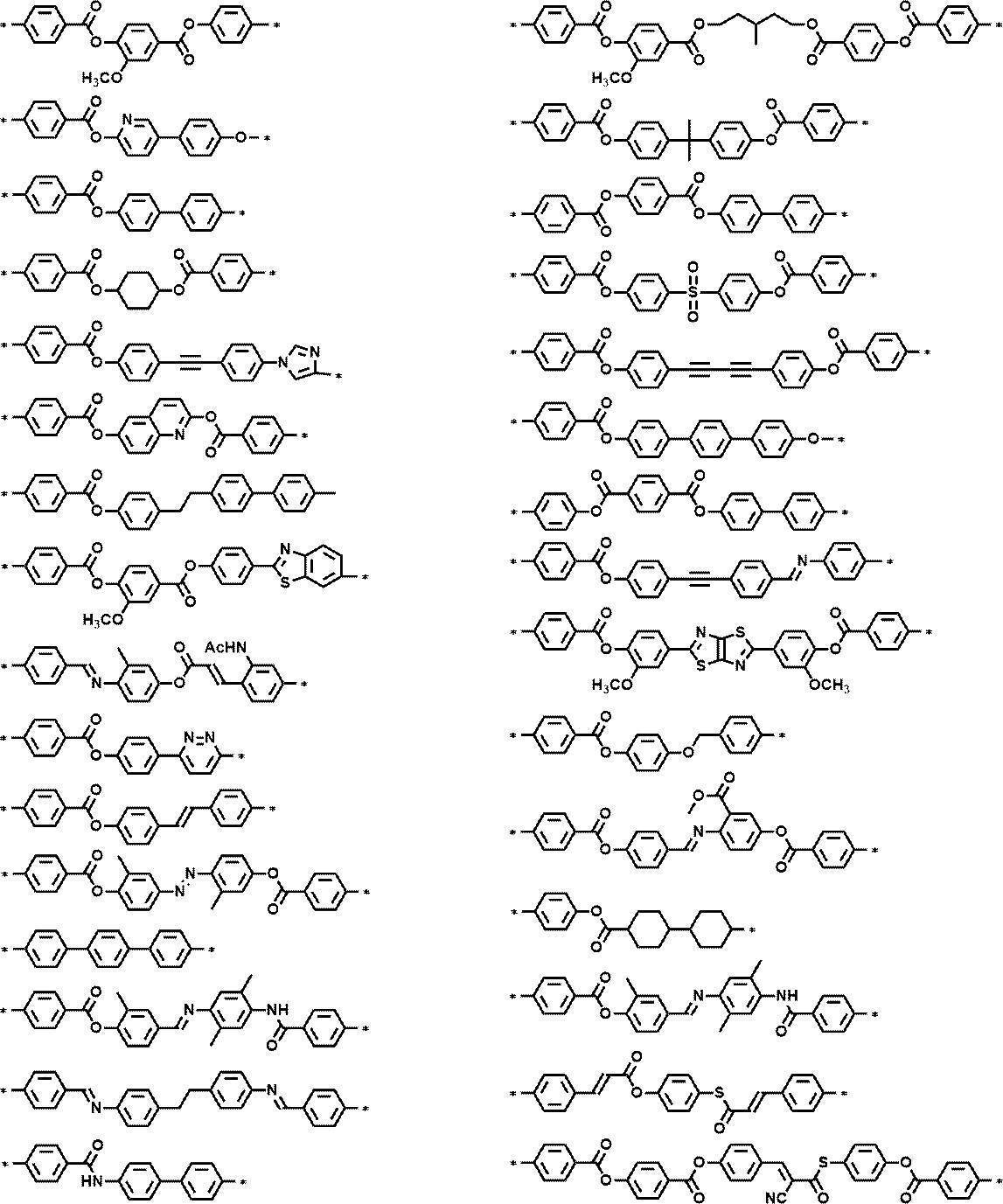
T1が表す末端基としては、水素原子、ハロゲン原子、シアノ基、ニトロ基、ヒドロキシ基、炭素数1~10のアルキル基、炭素数1~10のアルコキシ基、炭素数1~10のアルキルチオ基、炭素数1~10のアルコキシカルボニルオキシ基、炭素数1~10のアルコキシカルボニル基(ROC(O)-:Rはアルキル基)、炭素数1~10のアシルオキシ基、炭素数1~10のアシルアミノ基、炭素数1~10のアルコキシカルボニルアミノ基、炭素数1~10のスルホニルアミノ基、炭素数1~10のスルファモイル基、炭素数1~10のカルバモイル基、炭素数1~10のスルフィニル基、および、炭素数1~10のウレイド基、(メタ)アクリロイルオキシ基含有基等が挙げられる。上記(メタ)アクリロイルオキシ基含有基としては、例えば、-L-A(Lは単結合または連結基を表す。連結基の具体例は上述したL1およびSP1と同じである。Aは(メタ)アクリロイルオキシ基を表す)で表される基が挙げられる。
T1は、光吸収異方性層における二色性物質の配向度がより優れる点で、炭素数1~10のアルコキシ基が好ましく、炭素数1~5のアルコキシがより好ましく、メトキシ基がさらに好ましい。これらの末端基は、これらの基、または、上述の架橋性基によって、さらに置換されていてもよい。
T1の主鎖の原子数は、光吸収異方性層における二色性物質の配向度がより優れる点で、1~20が好ましく、1~15がより好ましく、1~10がさらに好ましく、1~7が特に好ましい。T1の主鎖の原子数が20以下であることで、光吸収異方性層における二色性物質の配向度がより向上する。ここで、T1おける「主鎖」とは、M1と結合する最も長い分子鎖を意味し、水素原子はT1の主鎖の原子数にカウントしない。例えば、T1がn-ブチル基である場合には主鎖の原子数は4であり、T1がsec-ブチル基である場合の主鎖の原子数は3である。
T1は、光吸収異方性層における二色性物質の配向度がより優れる点で、炭素数1~10のアルコキシ基が好ましく、炭素数1~5のアルコキシがより好ましく、メトキシ基がさらに好ましい。これらの末端基は、これらの基、または、上述の架橋性基によって、さらに置換されていてもよい。
T1の主鎖の原子数は、光吸収異方性層における二色性物質の配向度がより優れる点で、1~20が好ましく、1~15がより好ましく、1~10がさらに好ましく、1~7が特に好ましい。T1の主鎖の原子数が20以下であることで、光吸収異方性層における二色性物質の配向度がより向上する。ここで、T1おける「主鎖」とは、M1と結合する最も長い分子鎖を意味し、水素原子はT1の主鎖の原子数にカウントしない。例えば、T1がn-ブチル基である場合には主鎖の原子数は4であり、T1がsec-ブチル基である場合の主鎖の原子数は3である。
繰り返し単位(1L)の含有量は、光吸収異方性層における二色性物質の配向度がより優れる点で、高分子液晶性化合物が有する全繰り返し単位100質量%に対して、20~100質量%が好ましい。
本発明において、高分子液晶性化合物に含まれる各繰り返し単位の含有量は、各繰り返し単位を得るために使用される各単量体の仕込み量(質量)に基づいて算出される。
繰り返し単位(1L)は、高分子液晶性化合物中において、1種単独で含まれていてもよいし、2種以上含まれていてもよい。なかでも、光吸収異方性層における二色性物質の配向度がより優れる点で、繰り返し単位(1L)が高分子液晶性化合物中に2種含まれているのがよい。
本発明において、高分子液晶性化合物に含まれる各繰り返し単位の含有量は、各繰り返し単位を得るために使用される各単量体の仕込み量(質量)に基づいて算出される。
繰り返し単位(1L)は、高分子液晶性化合物中において、1種単独で含まれていてもよいし、2種以上含まれていてもよい。なかでも、光吸収異方性層における二色性物質の配向度がより優れる点で、繰り返し単位(1L)が高分子液晶性化合物中に2種含まれているのがよい。
高分子液晶性化合物が繰り返し単位(1L)を2種含む場合、光吸収異方性層における二色性物質の配向度がより優れる点で、一方(繰り返し単位A)においてT1が表す末端基がアルコキシ基であり、他方(繰り返し単位B)においてT1が表す末端基がアルコキシ基以外の基であることが好ましい。
上記繰り返し単位BにおいてT1が表す末端基は、光吸収異方性層における二色性物質の配向度がより優れる点で、アルコキシカルボニル基、シアノ基、または、(メタ)アクリロイルオキシ基含有基であることが好ましく、アルコキシカルボニル基、または、シアノ基であることがより好ましい。
高分子液晶性化合物中の上記繰り返し単位Aの含有量と高分子液晶性化合物中の上記繰り返し単位Bの含有量との割合(A/B)は、光吸収異方性層における二色性物質の配向度がより優れる点で、50/50~95/5であることが好ましく、60/40~93/7であることがより好ましく、70/30~90/10であることがさらに好ましい。
上記繰り返し単位BにおいてT1が表す末端基は、光吸収異方性層における二色性物質の配向度がより優れる点で、アルコキシカルボニル基、シアノ基、または、(メタ)アクリロイルオキシ基含有基であることが好ましく、アルコキシカルボニル基、または、シアノ基であることがより好ましい。
高分子液晶性化合物中の上記繰り返し単位Aの含有量と高分子液晶性化合物中の上記繰り返し単位Bの含有量との割合(A/B)は、光吸収異方性層における二色性物質の配向度がより優れる点で、50/50~95/5であることが好ましく、60/40~93/7であることがより好ましく、70/30~90/10であることがさらに好ましい。
また、高分子液晶性化合物は、繰り返し単位(1L)とももに、メソゲン基を有しない繰り返し単位を有していてもよい。メソゲン基を有しない繰り返し単位としては、式(1L)におけるM1が単結合である繰り返し単位が挙げられる。
高分子液晶性化合物がメソゲン基を有しない繰り返し単位を有する場合、光吸収異方性層における二色性物質の配向度がより優れる点で、高分子液晶性化合物が有する全繰り返し単位100質量%に対して、0質量%超30質量%以下が好ましく、10質量%超20質量%以下がより好ましい。
高分子液晶性化合物がメソゲン基を有しない繰り返し単位を有する場合、光吸収異方性層における二色性物質の配向度がより優れる点で、高分子液晶性化合物が有する全繰り返し単位100質量%に対して、0質量%超30質量%以下が好ましく、10質量%超20質量%以下がより好ましい。
-重量平均分子量-
高分子液晶性化合物の重量平均分子量(Mw)は、光吸収異方性層における二色性物質の配向度がより優れる点で、1000~500000が好ましく、2000~300000がより好ましい。高分子液晶性化合物のMwが上記範囲内にあれば、高分子液晶性化合物の取り扱いが容易になる。
特に、塗布時のクラック抑制の点で、高分子液晶性化合物の重量平均分子量(Mw)は、10000以上が好ましく、10000~300000がより好ましい。
また、配向度の温度ラチチュードの点で、高分子液晶性化合物の重量平均分子量(Mw)は、10000未満が好ましく、2000以上10000未満が好ましい。
ここで、本発明における重量平均分子量および数平均分子量は、ゲル浸透クロマトグラフ(GPC)法により測定された値である。
・溶媒(溶離液):N-メチルピロリドン
・装置名:TOSOH HLC-8220GPC
・カラム:TOSOH TSKgelSuperAWM-H(6mm×15cm)を3本接続して使用
・カラム温度:25℃
・試料濃度:0.1質量%
・流速:0.35mL/min
・校正曲線:TOSOH製TSK標準ポリスチレン Mw=2800000~1050(Mw/Mn=1.03~1.06)までの7サンプルによる校正曲線を使用
高分子液晶性化合物の重量平均分子量(Mw)は、光吸収異方性層における二色性物質の配向度がより優れる点で、1000~500000が好ましく、2000~300000がより好ましい。高分子液晶性化合物のMwが上記範囲内にあれば、高分子液晶性化合物の取り扱いが容易になる。
特に、塗布時のクラック抑制の点で、高分子液晶性化合物の重量平均分子量(Mw)は、10000以上が好ましく、10000~300000がより好ましい。
また、配向度の温度ラチチュードの点で、高分子液晶性化合物の重量平均分子量(Mw)は、10000未満が好ましく、2000以上10000未満が好ましい。
ここで、本発明における重量平均分子量および数平均分子量は、ゲル浸透クロマトグラフ(GPC)法により測定された値である。
・溶媒(溶離液):N-メチルピロリドン
・装置名:TOSOH HLC-8220GPC
・カラム:TOSOH TSKgelSuperAWM-H(6mm×15cm)を3本接続して使用
・カラム温度:25℃
・試料濃度:0.1質量%
・流速:0.35mL/min
・校正曲線:TOSOH製TSK標準ポリスチレン Mw=2800000~1050(Mw/Mn=1.03~1.06)までの7サンプルによる校正曲線を使用
(二色性物質)
本発明の光吸収異方性層は、二色性物質を含有することが好ましい。
二色性物質は、方向によって吸光度が異なる物質を意味する。二色性物質は特に限定されず、例えば、可視光吸収物質(例えば、二色性色素化合物および二色性アゾ色素化合物)、発光物質(例えば、蛍光物質および燐光物質)、紫外線吸収物質、赤外線吸収物質、非線形光学物質、カーボンナノチューブ、および、無機物質(例えば量子ロッド)等が挙げられ、従来公知の二色性物質(二色性色素化合物)を使用することができる。
本発明の光吸収異方性層は、二色性物質を含有することが好ましい。
二色性物質は、方向によって吸光度が異なる物質を意味する。二色性物質は特に限定されず、例えば、可視光吸収物質(例えば、二色性色素化合物および二色性アゾ色素化合物)、発光物質(例えば、蛍光物質および燐光物質)、紫外線吸収物質、赤外線吸収物質、非線形光学物質、カーボンナノチューブ、および、無機物質(例えば量子ロッド)等が挙げられ、従来公知の二色性物質(二色性色素化合物)を使用することができる。
なかでも、二色性色素化合物が好ましく、二色性アゾ色素化合物がより好ましい。
二色性アゾ色素化合物は、特に限定されず、従来公知の二色性アゾ色素化合物を使用することができるが、後述の化合物が好ましく用いられる。
以下、二色性アゾ色素化合物について説明する。
二色性アゾ色素化合物は、特に限定されず、従来公知の二色性アゾ色素化合物を使用することができるが、後述の化合物が好ましく用いられる。
以下、二色性アゾ色素化合物について説明する。
二色性アゾ色素化合物は、液晶性を示してもよく、液晶性を示さなくてもよい。
二色性アゾ色素化合物が液晶性を示す場合には、ネマチック性またはスメクチック性のいずれを示してもよい。液晶相を示す温度範囲は、室温以上300℃以下が好ましく、取扱い性および製造適性の点で、50~200℃がより好ましい。
二色性アゾ色素化合物が液晶性を示す場合には、ネマチック性またはスメクチック性のいずれを示してもよい。液晶相を示す温度範囲は、室温以上300℃以下が好ましく、取扱い性および製造適性の点で、50~200℃がより好ましい。
二色性アゾ色素化合物は、色味調整の点で、光吸収異方性層が、波長560~700nmの範囲に極大吸収波長を有する少なくとも1種の色素化合物(以下、「第1の二色性アゾ色素化合物」ともいう。)と、波長455nm以上560nm未満の範囲に極大吸収波長を有する少なくとも1種の色素化合物(以下、「第2の二色性アゾ色素化合物」ともいう。)とを少なくとも有していることが好ましく、具体的には、後述する式(3)で表される二色性アゾ色素化合物と、後述する式(4)で表される二色性アゾ色素化合物とを少なくとも有していることがより好ましい。
また、3種以上の二色性アゾ色素化合物を併用してもよく、例えば、光吸収異方性層を黒色に近づける点で、第1の二色性アゾ色素化合物と、第2の二色性アゾ色素化合物と、波長380nm以上455nm未満の範囲に極大吸収波長を有する少なくとも1種の色素化合物(以下、「第3の二色性アゾ色素化合物」とも略す。)とを併用することが好ましい。
また、耐押圧性が良好となる点で、二色性アゾ色素化合物は、架橋性基を有することが好ましい。
架橋性基としては、例えば、(メタ)アクリロイル基、エポキシ基、オキセタニル基、および、スチリル基等が挙げられ、なかでも、(メタ)アクリロイル基が好ましい。
架橋性基としては、例えば、(メタ)アクリロイル基、エポキシ基、オキセタニル基、および、スチリル基等が挙げられ、なかでも、(メタ)アクリロイル基が好ましい。
-第1の二色性アゾ色素化合物-
第1の二色性アゾ色素化合物は、上述した通り、波長560~700nmの範囲に極大吸収波長を有する二色性アゾ色素化合物である。
第1の二色性アゾ色素化合物は、波長560~700nmの範囲に最大吸収波長を有する二色性アゾ色素化合物であることが好ましく、偏光子の色味調整の点から、波長560~650nmの範囲に最大吸収波長を有する二色性アゾ色素化合物であることがより好ましく、波長560~640nmの範囲に最大吸収波長を有する二色性アゾ色素化合物であるのがさらに好ましい。
本明細書における二色性アゾ色素化合物の最大吸収波長(nm)は、二色性アゾ色素化合物を良溶媒中に溶解させた溶液を用いて、分光光度計によって測定される波長380~800nmの範囲における紫外可視光スペクトルから求められる。
第1の二色性アゾ色素化合物は、発色団と、発色団の末端に結合する側鎖とを有する化合物であることが好ましい。
発色団の具体例としては、芳香族環基(例えば、芳香族炭化水素基、芳香族複素環基)、アゾ基等が挙げられ、芳香族環基およびアゾ基の両方を有する構造が好ましく、芳香族複素環基(好ましくはチエノチアゾール基)と2つのアゾ基を有するビスアゾ構造がより好ましい。
側鎖としては、特に限定されず、後述の式(3)のL3、R2またはL4で表される基が挙げられる。
第1の二色性アゾ色素化合物は、上述した通り、波長560~700nmの範囲に極大吸収波長を有する二色性アゾ色素化合物である。
第1の二色性アゾ色素化合物は、波長560~700nmの範囲に最大吸収波長を有する二色性アゾ色素化合物であることが好ましく、偏光子の色味調整の点から、波長560~650nmの範囲に最大吸収波長を有する二色性アゾ色素化合物であることがより好ましく、波長560~640nmの範囲に最大吸収波長を有する二色性アゾ色素化合物であるのがさらに好ましい。
本明細書における二色性アゾ色素化合物の最大吸収波長(nm)は、二色性アゾ色素化合物を良溶媒中に溶解させた溶液を用いて、分光光度計によって測定される波長380~800nmの範囲における紫外可視光スペクトルから求められる。
第1の二色性アゾ色素化合物は、発色団と、発色団の末端に結合する側鎖とを有する化合物であることが好ましい。
発色団の具体例としては、芳香族環基(例えば、芳香族炭化水素基、芳香族複素環基)、アゾ基等が挙げられ、芳香族環基およびアゾ基の両方を有する構造が好ましく、芳香族複素環基(好ましくはチエノチアゾール基)と2つのアゾ基を有するビスアゾ構造がより好ましい。
側鎖としては、特に限定されず、後述の式(3)のL3、R2またはL4で表される基が挙げられる。
形成される光吸収異方性層における二色性アゾ色素化合物の配向度がさらに向上する点で、第1の二色性アゾ色素化合物が、下記式(3)で表される化合物が好ましい。

式(3)中、A4は、置換基を有していてもよい2価の芳香族基を表す。
式(3)中、L3およびL4は、それぞれ独立に、置換基を表す。
式(3)中、Eは、窒素原子、酸素原子および硫黄原子のいずれかの原子を表す。
式(3)中、R1は、水素原子、ハロゲン原子、置換基を有していてもよいアルキル基または置換基を有していてもよいアルコキシ基を表す。
式(3)中、R2は、水素原子または置換基を有していてもよいアルキル基を表す。
式(3)中、R3は、水素原子または置換基を表す。
式(3)中、nは、0または1を表す。ただし、Eが窒素原子である場合には、nは1であり、Eが酸素原子または硫黄原子である場合には、nは0である。
なお、上記置換基は、置換基Wが好ましい。
式(3)中、L3およびL4は、それぞれ独立に、置換基を表す。
式(3)中、Eは、窒素原子、酸素原子および硫黄原子のいずれかの原子を表す。
式(3)中、R1は、水素原子、ハロゲン原子、置換基を有していてもよいアルキル基または置換基を有していてもよいアルコキシ基を表す。
式(3)中、R2は、水素原子または置換基を有していてもよいアルキル基を表す。
式(3)中、R3は、水素原子または置換基を表す。
式(3)中、nは、0または1を表す。ただし、Eが窒素原子である場合には、nは1であり、Eが酸素原子または硫黄原子である場合には、nは0である。
なお、上記置換基は、置換基Wが好ましい。
式(3)中、A4が表す「置換基を有していてもよい2価の芳香族基」について説明する。
上記置換基としては、例えば、特開2011-237513号公報の[0237]~[0240]段落に記載された置換基群Gが挙げられ、中でも、ハロゲン原子、アルキル基、アルコキシ基、アルコキシカルボニル基(例えば、メトキシカルボニル、エトキシカルボニルなど)、アリールオキシカルボニル基(例えば、フェノキシカルボニル、4-メチルフェノキシカルボニル、4-メトキシフェニルカルボニルなど)等が好適に挙げられ、アルキル基がより好適に挙げられ、炭素数1~5のアルキル基がさらに好適に挙げられる。
一方、2価の芳香族基としては、例えば、2価の芳香族炭化水素基および2価の芳香族複素環基が挙げられる。
上記2価の芳香族炭化水素基としては、例えば、炭素数6~12のアリーレン基が挙げられ、具体的には、フェニレン基、クメニレン基、メシチレン基、トリレン基、キシリレン基等が挙げられる。中でもフェニレン基が好ましい。
上記置換基としては、例えば、特開2011-237513号公報の[0237]~[0240]段落に記載された置換基群Gが挙げられ、中でも、ハロゲン原子、アルキル基、アルコキシ基、アルコキシカルボニル基(例えば、メトキシカルボニル、エトキシカルボニルなど)、アリールオキシカルボニル基(例えば、フェノキシカルボニル、4-メチルフェノキシカルボニル、4-メトキシフェニルカルボニルなど)等が好適に挙げられ、アルキル基がより好適に挙げられ、炭素数1~5のアルキル基がさらに好適に挙げられる。
一方、2価の芳香族基としては、例えば、2価の芳香族炭化水素基および2価の芳香族複素環基が挙げられる。
上記2価の芳香族炭化水素基としては、例えば、炭素数6~12のアリーレン基が挙げられ、具体的には、フェニレン基、クメニレン基、メシチレン基、トリレン基、キシリレン基等が挙げられる。中でもフェニレン基が好ましい。
式(3)中、L3およびL4が表す置換基としては、置換基Wが挙げられる。中でも、置換基は、置換基を有していてもよいアルキル基、置換基を有していてもよいアルケニル基、置換基を有していてもよいアルキニル基、置換基を有していてもよいアリール基、置換基を有していてもよいアルコキシ基、置換基を有していてもよいオキシカルボニル基、置換基を有していてもよいアシルオキシ基、置換基を有していてもよいアシルアミノ基、置換基を有していてもよいアミノ基、置換基を有していてもよいアルコキシカルボニルアミノ基、置換基を有していてもよいスルホニルアミノ基、置換基を有していてもよいスルファモイル基、置換基を有していてもよいカルバモイル基、置換基を有していてもよいアルキルチオ基、置換基を有していてもよいスルホニル基、置換基を有していてもよいウレイド基、ニトロ基、ヒドロキシ基、シアノ基、イミノ基、アゾ基、ハロゲン原子、または、ヘテロ環基が好ましく、置換基を有していてもよいアルキル基、置換基を有していてもよいアルケニル基、置換基を有していてもよいアリール基、置換基を有していてもよいアルコキシ基、置換基を有していてもよいオキシカルボニル基、置換基を有していてもよいアシルオキシ基、置換基を有していてもよいアミノ基、ニトロ基、イミノ基、または、アゾ基がより好ましい。
L3およびL4の少なくとも一方は、架橋性基(重合性基)を含むことが好ましく、L3およびL4の両方に架橋性基を含むことがより好ましい。
架橋性基としては、具体的には、特開2010-244038号公報の[0040]~[0050]段落に記載された重合性基が挙げられ、反応性および合成適性の観点から、アクリロイル基、メタクリロイル基、エポキシ基、オキセタニル基、または、スチリル基が好ましく、アクリロイル基、または、メタクリロイル基が好ましい。
L3およびL4の少なくとも一方は、架橋性基(重合性基)を含むことが好ましく、L3およびL4の両方に架橋性基を含むことがより好ましい。
架橋性基としては、具体的には、特開2010-244038号公報の[0040]~[0050]段落に記載された重合性基が挙げられ、反応性および合成適性の観点から、アクリロイル基、メタクリロイル基、エポキシ基、オキセタニル基、または、スチリル基が好ましく、アクリロイル基、または、メタクリロイル基が好ましい。
式(3)中、Eは、窒素原子、酸素原子および硫黄原子のいずれかの原子を表し、合成適性の観点から、窒素原子であることが好ましい。
式(3)中、R1は、水素原子、ハロゲン原子、置換基を有していてもよいアルキル基および置換基を有していてもよいアルコキシ基のいずれかの基または原子を表し、水素原子または置換基を有してもよいアルキル基が好ましい。
上記置換基としては、例えば、ハロゲン原子等が挙げられる。
アルキル基としては、炭素数1~8の直鎖状、分岐鎖状または環状のアルキル基が挙げられる。中でも、炭素数1~6の直鎖状のアルキル基が好ましく、炭素数1~3の直鎖状のアルキル基がより好ましく、メチル基またはエチル基がさらに好ましい。
アルコキシ基としては、炭素数1~8のアルコキシ基が挙げられる。中でも、炭素数1~6のアルコキシ基が好ましく、炭素数1~3のアルコキシ基がより好ましく、メトキシ基またはエトキシ基がさらに好ましい。
上記置換基としては、例えば、ハロゲン原子等が挙げられる。
アルキル基としては、炭素数1~8の直鎖状、分岐鎖状または環状のアルキル基が挙げられる。中でも、炭素数1~6の直鎖状のアルキル基が好ましく、炭素数1~3の直鎖状のアルキル基がより好ましく、メチル基またはエチル基がさらに好ましい。
アルコキシ基としては、炭素数1~8のアルコキシ基が挙げられる。中でも、炭素数1~6のアルコキシ基が好ましく、炭素数1~3のアルコキシ基がより好ましく、メトキシ基またはエトキシ基がさらに好ましい。
式(3)中、R2は、水素原子または置換基を有していてもよいアルキル基を表し、置換基を有していてもよいアルキル基であることが好ましい。
R2が表す「置換基を有していてもよいアルキル基」の具体例および好適態様は、上述した式(3)のR1における「置換基を有していてもよいアルキル基」と同様であるので、その説明を省略する。
R2が表す「置換基を有していてもよいアルキル基」の具体例および好適態様は、上述した式(3)のR1における「置換基を有していてもよいアルキル基」と同様であるので、その説明を省略する。
式(3)中、R3は、水素原子または置換基を表す。
R3が表す「置換基」の具体例および好適態様は、上述した「置換基を有していてもよい2価の芳香族基」における置換基と同じであり、好ましい態様も同じであるので、その説明を省略する。
R3が表す「置換基」の具体例および好適態様は、上述した「置換基を有していてもよい2価の芳香族基」における置換基と同じであり、好ましい態様も同じであるので、その説明を省略する。
耐光性の点では、L3は電子吸引性基であることが好ましく、R2およびL4は電子供与性が低い基であることが好ましい。
このような基の具体例として、L3としては、アルキルスルホニル基、アルキルカルボニル基、アルキルオキシカルボニル基、アシルオキシ基、アルキルスルホニルアミノ基、アルキルスルファモイル基、アルキルスルフィニル基、および、アルキルウレイド基等が挙げられ、R2およびL4としては、下記の構造の基等が挙げられる。なお、下記の構造の基は、上記式(3)において、R2およびL4が結合する窒素原子を含む形で示す。
このような基の具体例として、L3としては、アルキルスルホニル基、アルキルカルボニル基、アルキルオキシカルボニル基、アシルオキシ基、アルキルスルホニルアミノ基、アルキルスルファモイル基、アルキルスルフィニル基、および、アルキルウレイド基等が挙げられ、R2およびL4としては、下記の構造の基等が挙げられる。なお、下記の構造の基は、上記式(3)において、R2およびL4が結合する窒素原子を含む形で示す。
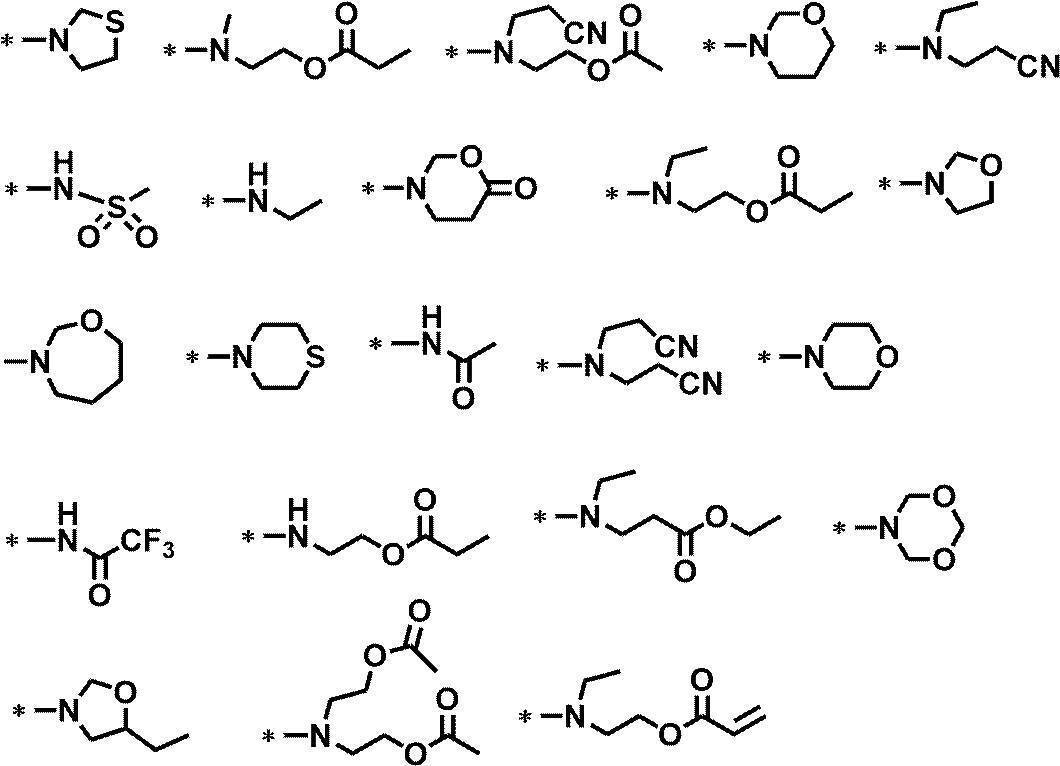
第1の二色性アゾ色素化合物の具体例を以下に示すが、これらに限定されるものではない。
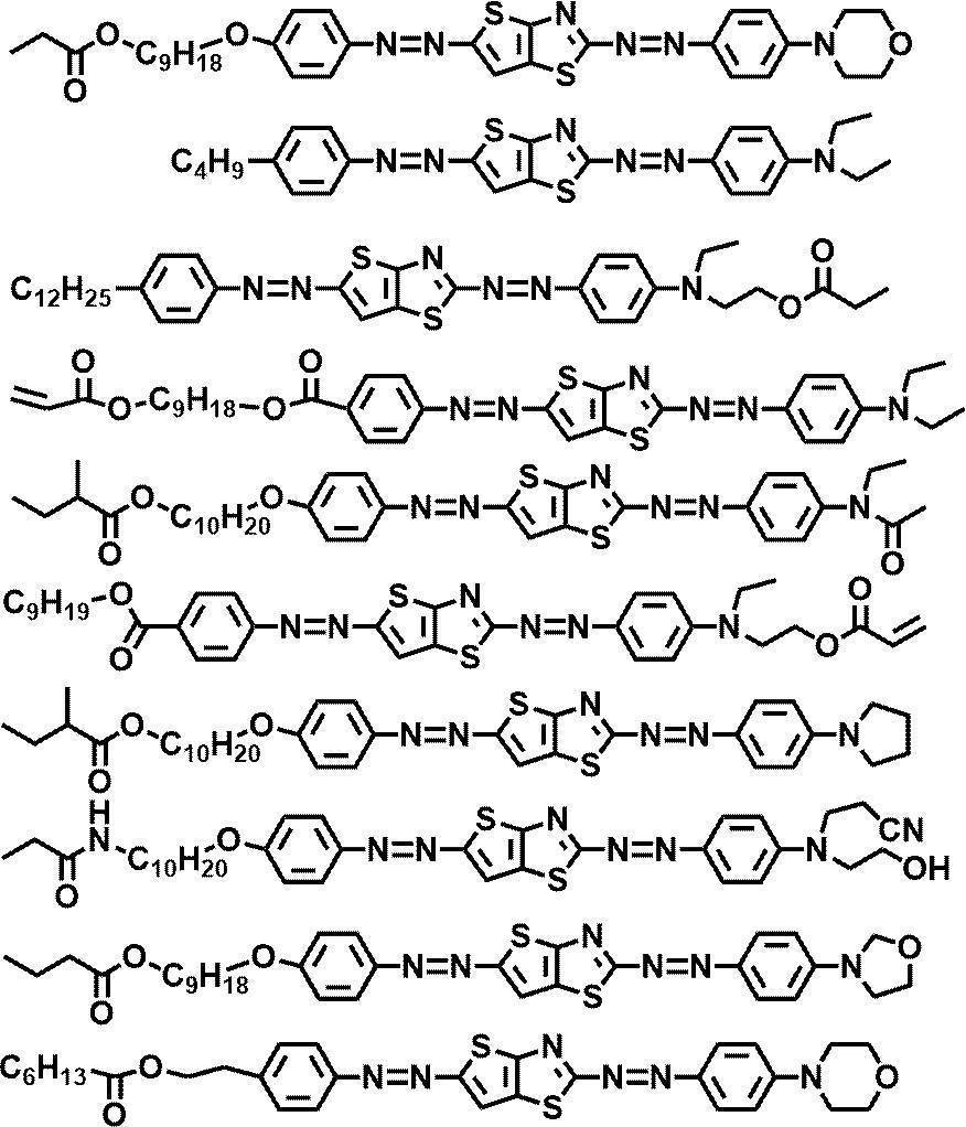

-第2の二色性アゾ色素化合物-
第2の二色性アゾ色素化合物は、第1の二色性アゾ色素化合物と異なる化合物であり、具体的にはその化学構造が異なっている。
また、第2の二色性アゾ色素化合物は、上述した通り、波長455nm以上560nm未満の範囲に極大吸収波長を有する二色性アゾ色素化合物である。
第2の二色性アゾ色素化合物は、偏光子の色味調整の点から、波長455nm以上560nm未満の範囲に最大吸収波長を有する二色性アゾ色素化合物であることが好ましく、波長455~555nmの範囲に最大吸収波長を有する二色性アゾ色素化合物であることがより好ましく、波長455~550nmの範囲に最大吸収波長を有する二色性アゾ色素化合物であることがさらに好ましい。
特に、最大吸収波長が560~700nmである第1の二色性アゾ色素化合物と、最大吸収波長が455nm以上560nm未満の第2の二色性アゾ色素化合物と、を用いれば、偏光子の色味調整がより容易になる。
第2の二色性アゾ色素化合物は、二色性アゾ色素化合物の核である発色団と、発色団の末端に結合する側鎖と、を有する化合物であることが好ましい。
発色団の具体例としては、芳香族環基(例えば、芳香族炭化水素基、芳香族複素環基)、アゾ基等が挙げられ、芳香族炭化水素基およびアゾ基の両方を有する構造が好ましく、芳香族炭化水素基と2または3つのアゾ基とを有するビスアゾまたはトリスアゾ構造がより好ましい。
側鎖としては、特に限定されず、後述の式(4)のR4、R5またはR6で表される基が挙げられる。
第2の二色性アゾ色素化合物は、第1の二色性アゾ色素化合物と異なる化合物であり、具体的にはその化学構造が異なっている。
また、第2の二色性アゾ色素化合物は、上述した通り、波長455nm以上560nm未満の範囲に極大吸収波長を有する二色性アゾ色素化合物である。
第2の二色性アゾ色素化合物は、偏光子の色味調整の点から、波長455nm以上560nm未満の範囲に最大吸収波長を有する二色性アゾ色素化合物であることが好ましく、波長455~555nmの範囲に最大吸収波長を有する二色性アゾ色素化合物であることがより好ましく、波長455~550nmの範囲に最大吸収波長を有する二色性アゾ色素化合物であることがさらに好ましい。
特に、最大吸収波長が560~700nmである第1の二色性アゾ色素化合物と、最大吸収波長が455nm以上560nm未満の第2の二色性アゾ色素化合物と、を用いれば、偏光子の色味調整がより容易になる。
第2の二色性アゾ色素化合物は、二色性アゾ色素化合物の核である発色団と、発色団の末端に結合する側鎖と、を有する化合物であることが好ましい。
発色団の具体例としては、芳香族環基(例えば、芳香族炭化水素基、芳香族複素環基)、アゾ基等が挙げられ、芳香族炭化水素基およびアゾ基の両方を有する構造が好ましく、芳香族炭化水素基と2または3つのアゾ基とを有するビスアゾまたはトリスアゾ構造がより好ましい。
側鎖としては、特に限定されず、後述の式(4)のR4、R5またはR6で表される基が挙げられる。
第2の二色性アゾ色素化合物は、偏光子の配向度がより向上する点から、式(4)で表される化合物であるのが好ましい。
式(4)

式(4)中、nは1または2を表す。
式(4)中、Ar3、Ar4およびAr5はそれぞれ独立に、置換基を有していてもよいフェニレン基、または、置換基を有していてもよい複素環基を表す。置換基としては、特に制限されないが、例えば、置換基Wが挙げられる。
複素環基としては、芳香族および非芳香族のいずれであってもよい。
芳香族複素環基を構成する炭素以外の原子としては、窒素原子、硫黄原子および酸素原子が挙げられる。芳香族複素環基が炭素以外の環を構成する原子を複数有する場合、これらは同一であっても異なっていてもよい。
芳香族複素環基の具体例としては、例えば、ピリジレン基(ピリジン-ジイル基)、ピリダジン-ジイル基、イミダゾール-ジイル基、チエニレン(チオフェン-ジイル基)、キノリレン基(キノリン-ジイル基)、イソキノリレン基(イソキノリン-ジイル基)、オキサゾール-ジイル基、チアゾール-ジイル基、オキサジアゾール-ジイル基、ベンゾチアゾール-ジイル基、ベンゾチアジアゾール-ジイル基、フタルイミド-ジイル基、チエノチアゾール-ジイル基、チアゾロチアゾール-ジイル基、チエノチオフェン-ジイル基、および、チエノオキサゾール-ジイル基等が挙げられる。
式(4)中、Ar3、Ar4およびAr5はそれぞれ独立に、置換基を有していてもよいフェニレン基、または、置換基を有していてもよい複素環基を表す。置換基としては、特に制限されないが、例えば、置換基Wが挙げられる。
複素環基としては、芳香族および非芳香族のいずれであってもよい。
芳香族複素環基を構成する炭素以外の原子としては、窒素原子、硫黄原子および酸素原子が挙げられる。芳香族複素環基が炭素以外の環を構成する原子を複数有する場合、これらは同一であっても異なっていてもよい。
芳香族複素環基の具体例としては、例えば、ピリジレン基(ピリジン-ジイル基)、ピリダジン-ジイル基、イミダゾール-ジイル基、チエニレン(チオフェン-ジイル基)、キノリレン基(キノリン-ジイル基)、イソキノリレン基(イソキノリン-ジイル基)、オキサゾール-ジイル基、チアゾール-ジイル基、オキサジアゾール-ジイル基、ベンゾチアゾール-ジイル基、ベンゾチアジアゾール-ジイル基、フタルイミド-ジイル基、チエノチアゾール-ジイル基、チアゾロチアゾール-ジイル基、チエノチオフェン-ジイル基、および、チエノオキサゾール-ジイル基等が挙げられる。
式(4)中、R4の定義は、式(3)中のL3と同様である。
式(4)中、R5およびR6の定義はそれぞれ、式(3)中のR2およびL4と同様である。
式(4)中、R5およびR6の定義はそれぞれ、式(3)中のR2およびL4と同様である。
耐光性の点では、R4は電子吸引性基であることが好ましく、R5およびR6は電子供与性が低い基であることが好ましい。
このような基のうち、R4が電子吸引性基である場合の具体例は、L3が電子吸引性基である場合の具体例と同様であり、R5およびR6が電子供与性の低い基である場合の具体例は、R2およびL4が電子供与性の低い基である場合の具体例と同様である。
このような基のうち、R4が電子吸引性基である場合の具体例は、L3が電子吸引性基である場合の具体例と同様であり、R5およびR6が電子供与性の低い基である場合の具体例は、R2およびL4が電子供与性の低い基である場合の具体例と同様である。
第2の二色性アゾ色素化合物の具体例を以下に示すが、これに限定されるものではない。


-logP値の差-
logP値は、化学構造の親水性および疎水性の性質を表現する指標の一つである。
第1の二色性アゾ色素化合物の側鎖のlogP値と、第2の二色性アゾ色素化合物の側鎖のlogP値と、の差の絶対値(以下、「logP差」ともいう。)は、2.30以下が好ましく、2.0以下がより好ましく、1.5以下がさらに好ましく、1.0以下が特に好ましい。logP差が2.30以下であれば、第1の二色性アゾ色素化合物と第2の二色性アゾ色素化合物との親和性が高まって、配列構造をより形成しやすくなるため、二色性アゾ色素化合物の配向度がより向上する。
なお、第1の二色性アゾ色素化合物または第2の二色性アゾ色素化合物の側鎖が複数ある場合、少なくとも1つのlogP差が上記値を満たすことが好ましい。
ここで、第1の二色性アゾ色素化合物および第2の二色性アゾ色素化合物の側鎖とは、上述した発色団の末端に結合する基を意味する。例えば、第1の二色性アゾ色素化合物が式(3)で表される化合物である場合、式(3)中のL3、L4およびR2が側鎖であり、第2の二色性アゾ色素化合物が式(4)で表される化合物である場合、式(4)中のR4、R5およびR6が側鎖である。特に、第1の二色性アゾ色素化合物が式(3)で表される化合物であり、第2の二色性アゾ色素化合物が式(4)で表される化合物である場合、L3とR4とのlogP値の差、L3とR5とのlogP値の差、L4とR4とのlogP値の差、および、L4とR5とのlogP値の差のうち、少なくとも1つのlogP差が上記値を満たすことが好ましい。
logP値は、化学構造の親水性および疎水性の性質を表現する指標の一つである。
第1の二色性アゾ色素化合物の側鎖のlogP値と、第2の二色性アゾ色素化合物の側鎖のlogP値と、の差の絶対値(以下、「logP差」ともいう。)は、2.30以下が好ましく、2.0以下がより好ましく、1.5以下がさらに好ましく、1.0以下が特に好ましい。logP差が2.30以下であれば、第1の二色性アゾ色素化合物と第2の二色性アゾ色素化合物との親和性が高まって、配列構造をより形成しやすくなるため、二色性アゾ色素化合物の配向度がより向上する。
なお、第1の二色性アゾ色素化合物または第2の二色性アゾ色素化合物の側鎖が複数ある場合、少なくとも1つのlogP差が上記値を満たすことが好ましい。
ここで、第1の二色性アゾ色素化合物および第2の二色性アゾ色素化合物の側鎖とは、上述した発色団の末端に結合する基を意味する。例えば、第1の二色性アゾ色素化合物が式(3)で表される化合物である場合、式(3)中のL3、L4およびR2が側鎖であり、第2の二色性アゾ色素化合物が式(4)で表される化合物である場合、式(4)中のR4、R5およびR6が側鎖である。特に、第1の二色性アゾ色素化合物が式(3)で表される化合物であり、第2の二色性アゾ色素化合物が式(4)で表される化合物である場合、L3とR4とのlogP値の差、L3とR5とのlogP値の差、L4とR4とのlogP値の差、および、L4とR5とのlogP値の差のうち、少なくとも1つのlogP差が上記値を満たすことが好ましい。
また、logP値は、親疎水パラメータと呼ばれることがある。logP値は、ChemBioDraw UltraまたはHSPiP(Ver.4.1.07)等のソフトウェアを用いて計算できる。また、OECD Guidelines for the Testing of Chemicals,Sections 1,Test No.117の方法等により、実験的に求めることもできる。本明細書では特に断りのない限り、HSPiP(Ver.4.1.07)に化合物の構造式を入力して算出される値をlogP値として採用する。
-第3の二色性アゾ色素化合物-
第3の二色性アゾ色素化合物は、第1の二色性アゾ色素化合物および第2の二色性アゾ色素化合物以外の二色性アゾ色素化合物であり、具体的には、第1の二色性アゾ色素化合物および第2の二色性アゾ色素化合物とは化学構造が異なっている。光吸収異方性層が第3の二色性アゾ色素化合物を含有すれば、光吸収異方性層の色味の調整が容易になるという利点がある。
また、第3の二色性アゾ色素化合物は、上述した通り、波長380nm以上455nm未満の範囲に極大吸収波長を有する二色性アゾ色素化合物である。
第3の二色性アゾ色素化合物は、偏光子の色味調整の点から、波長380nm以上455nm未満の範囲に最大吸収波長を有する二色性アゾ色素化合物であることが好ましく、波長400~455nmの範囲に最大吸収波長を有する二色性アゾ色素化合物であることがより好ましく、波長410~455nmの範囲に最大吸収波長を有する二色性アゾ色素化合物であることがさらに好ましい。
第3の二色性アゾ色素化合物は、第1の二色性アゾ色素化合物および第2の二色性アゾ色素化合物以外の二色性アゾ色素化合物であり、具体的には、第1の二色性アゾ色素化合物および第2の二色性アゾ色素化合物とは化学構造が異なっている。光吸収異方性層が第3の二色性アゾ色素化合物を含有すれば、光吸収異方性層の色味の調整が容易になるという利点がある。
また、第3の二色性アゾ色素化合物は、上述した通り、波長380nm以上455nm未満の範囲に極大吸収波長を有する二色性アゾ色素化合物である。
第3の二色性アゾ色素化合物は、偏光子の色味調整の点から、波長380nm以上455nm未満の範囲に最大吸収波長を有する二色性アゾ色素化合物であることが好ましく、波長400~455nmの範囲に最大吸収波長を有する二色性アゾ色素化合物であることがより好ましく、波長410~455nmの範囲に最大吸収波長を有する二色性アゾ色素化合物であることがさらに好ましい。
第3の二色性アゾ色素化合物は、下記式(6)で表される二色性アゾ色素化合物を含有することが好ましい。
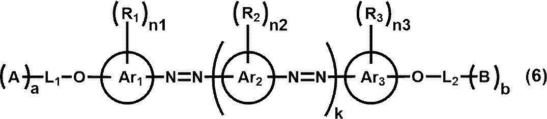
式(6)中、AおよびBは、それぞれ独立に、架橋性基、または、1価の置換基を表す。
式(6)中、aおよびbは、それぞれ独立に、0または1を表す。420nmの配向度に優れる点においては、aおよびbは、ともに0であることが好ましい。
式(6)中、a=0の場合にはL1は1価の置換基を表し、a=1の場合にはL1は単結合または2価の連結基を表す。また、b=0の場合にはL2は1価の置換基を表し、b=1の場合にはL2は単結合または2価の連結基を表す。
式(6)中、Ar1は(n1+2)価の芳香族炭化水素基または複素環基を表し、Ar2は(n2+2)価の芳香族炭化水素基または複素環基を表し、Ar3は(n3+2)価の芳香族炭化水素基または複素環基を表す。
式(6)中、R1、R2およびR3は、それぞれ独立に、1価の置換基を表す。n1≧2である場合には複数のR1は互いに同一でも異なっていてもよく、n2≧2である場合には複数のR2は互いに同一でも異なっていてもよく、n3≧2である場合には複数のR3は互いに同一でも異なっていてもよい。
式(6)中、kは、1~4の整数を表す。k≧2の場合には、複数のAr2は互いに同一でも異なっていてもよく、複数のR2は互いに同一でも異なっていてもよい。
式(6)中、n1、n2およびn3は、それぞれ独立に、0~4の整数を表す。ただし、k=1の場合にはn1+n2+n3≧0であり、k≧2の場合にはn1+n2+n3≧1である。
式(6)中、aおよびbは、それぞれ独立に、0または1を表す。420nmの配向度に優れる点においては、aおよびbは、ともに0であることが好ましい。
式(6)中、a=0の場合にはL1は1価の置換基を表し、a=1の場合にはL1は単結合または2価の連結基を表す。また、b=0の場合にはL2は1価の置換基を表し、b=1の場合にはL2は単結合または2価の連結基を表す。
式(6)中、Ar1は(n1+2)価の芳香族炭化水素基または複素環基を表し、Ar2は(n2+2)価の芳香族炭化水素基または複素環基を表し、Ar3は(n3+2)価の芳香族炭化水素基または複素環基を表す。
式(6)中、R1、R2およびR3は、それぞれ独立に、1価の置換基を表す。n1≧2である場合には複数のR1は互いに同一でも異なっていてもよく、n2≧2である場合には複数のR2は互いに同一でも異なっていてもよく、n3≧2である場合には複数のR3は互いに同一でも異なっていてもよい。
式(6)中、kは、1~4の整数を表す。k≧2の場合には、複数のAr2は互いに同一でも異なっていてもよく、複数のR2は互いに同一でも異なっていてもよい。
式(6)中、n1、n2およびn3は、それぞれ独立に、0~4の整数を表す。ただし、k=1の場合にはn1+n2+n3≧0であり、k≧2の場合にはn1+n2+n3≧1である。
式(6)において、AおよびBが表す架橋性基としては、例えば、特開2010-244038号公報の[0040]~[0050]段落に記載された重合性基が挙げられる。これらの中でも、反応性および合成適性の向上の観点から、アクリロイル基、メタクリロイル基、エポキシ基、オキセタニル基、および、スチリル基が好ましく、溶解性をより向上できるという観点から、アクリロイル基およびメタクリロイル基がより好ましい。
式(6)において、AおよびBが表す1価の置換基としては、例えば、置換基Wが挙げられる。
L1およびL2が表す1価の置換基としては、二色性物質の溶解性を高めるために導入される基、または、色素としての色調を調節するために導入される電子供与性や電子吸引性を有する基が好ましい。置換基としては、例えば、置換基Wが挙げられる。
置換基Wは、さらに置換基Wによって置換されていてもよい。また、置換基を2つ以上有する場合は、同じでも異なってもよい。また、可能な場合には互いに結合して環を形成していてもよい。
上記置換基Wがさらに上記置換基Wによって置換された基としては、例えば、アルコキシ基がアルキル基で置換された基である、RB-(O-RA)na-基、および、カルボキシ基がアルキル基で置換された基である、RB-OCO-RA-基が挙げられる。ここで、式中、RAは炭素数1~5のアルキレン基を表し、RBは炭素数1~5のアルキル基を表し、naは1~10(好ましくは1~5、より好ましくは1~3)の整数を表す。
なかでも、L1およびL2が表す1価の置換基としては、アルキル基、アルケニル基、アルコキシ基、および、これらの基がさらにこれらの基によって置換された基(例えば、上述したRB-(O-RA)na-基、および、RB-OCO-RA-基)が好ましく、アルキル基、アルコキシ基、および、これらの基がさらにこれらの基によって置換された基(例えば、上述したRB-(O-RA)na-基、および、RB-OCO-RA-基)がより好ましい。
置換基Wは、さらに置換基Wによって置換されていてもよい。また、置換基を2つ以上有する場合は、同じでも異なってもよい。また、可能な場合には互いに結合して環を形成していてもよい。
上記置換基Wがさらに上記置換基Wによって置換された基としては、例えば、アルコキシ基がアルキル基で置換された基である、RB-(O-RA)na-基、および、カルボキシ基がアルキル基で置換された基である、RB-OCO-RA-基が挙げられる。ここで、式中、RAは炭素数1~5のアルキレン基を表し、RBは炭素数1~5のアルキル基を表し、naは1~10(好ましくは1~5、より好ましくは1~3)の整数を表す。
なかでも、L1およびL2が表す1価の置換基としては、アルキル基、アルケニル基、アルコキシ基、および、これらの基がさらにこれらの基によって置換された基(例えば、上述したRB-(O-RA)na-基、および、RB-OCO-RA-基)が好ましく、アルキル基、アルコキシ基、および、これらの基がさらにこれらの基によって置換された基(例えば、上述したRB-(O-RA)na-基、および、RB-OCO-RA-基)がより好ましい。
L1およびL2が表す2価の連結基としては、例えば、-O-、-S-、-CO-、-COO-、-OCO-、-O-CO-O-、-CO-NRN-、-O-CO-NRN-、-NRN-CO-NRN-、-SO2-、-SO-、アルキレン基、シクロアルキレン基、および、アルケニレン基、ならびに、これらの基を2つ以上組み合わせた基等が挙げられる。
なかでも、アルキレン基と、-O-、-COO-、-OCO-、および、-O-CO-O-からなる群より選択される1種以上の基と、を組み合わせた基が好ましく、アルキレン基と、-OCO-を組み合わせた基が特に好ましい。
ここで、RNは、水素原子またはアルキル基を表す。RNが複数存在する場合には、複数のRNは互いに同一でも異なっていてもよい。
なかでも、アルキレン基と、-O-、-COO-、-OCO-、および、-O-CO-O-からなる群より選択される1種以上の基と、を組み合わせた基が好ましく、アルキレン基と、-OCO-を組み合わせた基が特に好ましい。
ここで、RNは、水素原子またはアルキル基を表す。RNが複数存在する場合には、複数のRNは互いに同一でも異なっていてもよい。
二色性物質の溶解性がより向上するという点で、L1およびL2の少なくとも一方の主鎖の原子の数は、3個以上であることが好ましく、5個以上であることがより好ましく、7個以上であることがさらに好ましく、10個以上であることが特に好ましい。また、主鎖の原子の数の上限値は、20個以下であることが好ましく、12個以下であることがより好ましい。
一方で、光吸収異方性層における二色性物質の配向度がより向上するという点では、L1およびL2の少なくとも一方の主鎖の原子の数は、1~5個であることが好ましい。
ここで、式(6)におけるAが存在する場合には、L1における「主鎖」とは、L1と連結する「O」原子と、「A」と、を直接連結するために必要な部分を指し、「主鎖の原子の数」とは、上記部分を構成する原子の個数のことを指す。同様に、式(6)におけるBが存在する場合には、L2における「主鎖」とは、L2と連結する「O」原子と、「B」と、を直接連結するために必要な部分を指し、「主鎖の原子の数」とは、上記部分を構成する原子の数のことを指す。なお、「主鎖の原子の数」には、後述する分岐鎖の原子の数は含まない。
また、Aが存在しない場合には、L1における「主鎖の原子の数」とは、分岐鎖を含まないL1の原子の個数のことをいう。Bが存在しない場合には、L2における「主鎖の原子の数」とは、分岐鎖を含まないL2の原子の個数のことをいう。
具体的には、下記式(D1)においては、L1の主鎖の原子の数は5個(下記式(D1)の左側の点線枠内の原子の数)であり、L2の主鎖の原子の数は5個(下記式(D1)の右側の点線枠内の原子の数)である。また、下記式(D10)においては、L1の主鎖の原子の数は7個(下記式(D10)の左側の点線枠内の原子の数)であり、L2の主鎖の原子の数は5個(下記式(D10)の右側の点線枠内の原子の数)である。
一方で、光吸収異方性層における二色性物質の配向度がより向上するという点では、L1およびL2の少なくとも一方の主鎖の原子の数は、1~5個であることが好ましい。
ここで、式(6)におけるAが存在する場合には、L1における「主鎖」とは、L1と連結する「O」原子と、「A」と、を直接連結するために必要な部分を指し、「主鎖の原子の数」とは、上記部分を構成する原子の個数のことを指す。同様に、式(6)におけるBが存在する場合には、L2における「主鎖」とは、L2と連結する「O」原子と、「B」と、を直接連結するために必要な部分を指し、「主鎖の原子の数」とは、上記部分を構成する原子の数のことを指す。なお、「主鎖の原子の数」には、後述する分岐鎖の原子の数は含まない。
また、Aが存在しない場合には、L1における「主鎖の原子の数」とは、分岐鎖を含まないL1の原子の個数のことをいう。Bが存在しない場合には、L2における「主鎖の原子の数」とは、分岐鎖を含まないL2の原子の個数のことをいう。
具体的には、下記式(D1)においては、L1の主鎖の原子の数は5個(下記式(D1)の左側の点線枠内の原子の数)であり、L2の主鎖の原子の数は5個(下記式(D1)の右側の点線枠内の原子の数)である。また、下記式(D10)においては、L1の主鎖の原子の数は7個(下記式(D10)の左側の点線枠内の原子の数)であり、L2の主鎖の原子の数は5個(下記式(D10)の右側の点線枠内の原子の数)である。

L1およびL2は、分岐鎖を有していてもよい。
ここで、式(6)においてAが存在する場合には、L1における「分岐鎖」とは、式(6)におけるL1と連結する「O」原子と、「A」と、を直接連結するために必要な部分以外の部分をいう。同様に、式(6)においてBが存在する場合には、L2における「分岐鎖」とは、式(6)におけるL2と連結する「O」原子と、「B」と、を直接連結するために必要な部分以外の部分をいう。
また、式(6)においてAが存在しない場合には、L1における「分岐鎖」とは、式(6)におけるL1と連結する「O」原子を起点として延びる最長の原子鎖(すなわち主鎖)以外の部分をいう。同様に、式(6)においてBが存在しない場合には、L2における「分岐鎖」とは、式(6)におけるL2と連結する「O」原子を起点として延びる最長の原子鎖(すなわち主鎖)以外の部分をいう。
分岐鎖の原子の数は、3以下であることが好ましい。分岐鎖の原子の数が3以下であることで、光吸収異方性層における二色性物質の配向度がより向上する等の利点がある。なお、分岐鎖の原子の数には、水素原子の数は含まれない。
ここで、式(6)においてAが存在する場合には、L1における「分岐鎖」とは、式(6)におけるL1と連結する「O」原子と、「A」と、を直接連結するために必要な部分以外の部分をいう。同様に、式(6)においてBが存在する場合には、L2における「分岐鎖」とは、式(6)におけるL2と連結する「O」原子と、「B」と、を直接連結するために必要な部分以外の部分をいう。
また、式(6)においてAが存在しない場合には、L1における「分岐鎖」とは、式(6)におけるL1と連結する「O」原子を起点として延びる最長の原子鎖(すなわち主鎖)以外の部分をいう。同様に、式(6)においてBが存在しない場合には、L2における「分岐鎖」とは、式(6)におけるL2と連結する「O」原子を起点として延びる最長の原子鎖(すなわち主鎖)以外の部分をいう。
分岐鎖の原子の数は、3以下であることが好ましい。分岐鎖の原子の数が3以下であることで、光吸収異方性層における二色性物質の配向度がより向上する等の利点がある。なお、分岐鎖の原子の数には、水素原子の数は含まれない。
式(6)において、Ar1は(n1+2)価(例えば、n1が1であるときは3価)、Ar2は(n2+2)価(例えば、n2が1であるときは3価)、Ar3は(n3+2)価(例えば、n3が1であるときは3価)、の芳香族炭化水素基または複素環基を表す。ここで、Ar1~Ar3はそれぞれ、n1~n3個の置換基(後述するR1~R3)で置換された2価の芳香族炭化水素基または2価の複素環基と換言できる。
Ar1~Ar3が表す2価の芳香族炭化水素基としては、単環であっても、2環以上の縮環構造を有していてもよい。2価の芳香族炭化水素基の環数は、溶解性がより向上するという観点から、1~4が好ましく、1~2がより好ましく、1(すなわちフェニレン基であること)がさらに好ましい。
2価の芳香族炭化水素基の具体例としては、フェニレン基、アズレン-ジイル基、ナフチレン基、フルオレン-ジイル基、アントラセン-ジイル基およびテトラセン-ジイル基などが挙げられ、溶解性がより向上するという観点から、フェニレン基およびナフチレン基が好ましく、フェニレン基がより好ましい。
以下に、第3の二色性色素化合物の具体例を示すが、本発明はこれらに限定されるものではない。なお、下記具体例中、nは、1~10の整数を表す。
Ar1~Ar3が表す2価の芳香族炭化水素基としては、単環であっても、2環以上の縮環構造を有していてもよい。2価の芳香族炭化水素基の環数は、溶解性がより向上するという観点から、1~4が好ましく、1~2がより好ましく、1(すなわちフェニレン基であること)がさらに好ましい。
2価の芳香族炭化水素基の具体例としては、フェニレン基、アズレン-ジイル基、ナフチレン基、フルオレン-ジイル基、アントラセン-ジイル基およびテトラセン-ジイル基などが挙げられ、溶解性がより向上するという観点から、フェニレン基およびナフチレン基が好ましく、フェニレン基がより好ましい。
以下に、第3の二色性色素化合物の具体例を示すが、本発明はこれらに限定されるものではない。なお、下記具体例中、nは、1~10の整数を表す。
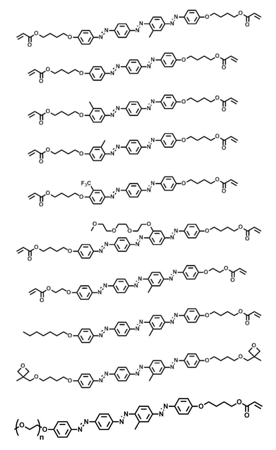

また、第3の色素がラジカル重合性基を有さない構造であることも好ましい。ラジカル重合性基を有さない構造である場合、後述する配向度の測定波長が420nmの場合の配向度に優れる。
ラジカル重合性基を有さない構造は、例えば、以下の構造が挙げられる。


ラジカル重合性基を有さない構造は、例えば、以下の構造が挙げられる。
第3の二色性アゾ色素化合物は、後述する配向度の測定波長が420nmの場合の配向度において特に優れる点で、下記式(1-1)で表される構造を有する二色性アゾ色素化合物であることがより好ましい。
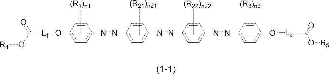
式(1-1)中、R1、R3、n1、n3、L1およびL2の定義はそれぞれ、式(6)のR1、R3、n1、n3、L1およびL2と同義である。
式(1-1)中、R4およびR5の定義は、置換基Wと同義である。
式(1-1)中、R21およびR22の定義はそれぞれ独立に、式(6)のR2と同義である。
式(1-1)中、n21およびn22の定義はそれぞれ独立に、式(6)のn2と同義である。
n1+n21+n22+n3≧1であり、n1+n21+n22+n3は、1~9が好ましく、1~5がより好ましい。
式(1-1)中、R4およびR5の定義は、置換基Wと同義である。
式(1-1)中、R21およびR22の定義はそれぞれ独立に、式(6)のR2と同義である。
式(1-1)中、n21およびn22の定義はそれぞれ独立に、式(6)のn2と同義である。
n1+n21+n22+n3≧1であり、n1+n21+n22+n3は、1~9が好ましく、1~5がより好ましい。
以下に、第3の二色性アゾ色素化合物の具体例を示すが、本発明はこれらに限定されるものではない。


[光吸収異方性層形成用組成物]
本発明の光学フィルムが有する光吸収異方性層は、例えば、液晶性化合物、および、二色性物質を含む光吸収異方性層形成用組成物を用いて作製することが好ましい。
光吸収異方性層形成用組成物は、液晶性化合物、および、二色性物質以外の成分を含んでいてもよく、例えば、溶媒、界面改良剤、垂直配向剤、重合性成分、重合開始剤(例えば、ラジカル重合開始剤)、垂直配向に適したレベリング剤等が挙げられる。この場合、本発明における光吸収異方性層は、液状成分(溶媒等)以外の固形成分を含む。
以下、光吸収異方性層形成用組成物が含んでいてよい成分について説明する。
なお、液晶性化合物、および、二色性物質は上述したものを用いることができ、好適態様も上述したとおりである。
本発明の光学フィルムが有する光吸収異方性層は、例えば、液晶性化合物、および、二色性物質を含む光吸収異方性層形成用組成物を用いて作製することが好ましい。
光吸収異方性層形成用組成物は、液晶性化合物、および、二色性物質以外の成分を含んでいてもよく、例えば、溶媒、界面改良剤、垂直配向剤、重合性成分、重合開始剤(例えば、ラジカル重合開始剤)、垂直配向に適したレベリング剤等が挙げられる。この場合、本発明における光吸収異方性層は、液状成分(溶媒等)以外の固形成分を含む。
以下、光吸収異方性層形成用組成物が含んでいてよい成分について説明する。
なお、液晶性化合物、および、二色性物質は上述したものを用いることができ、好適態様も上述したとおりである。
(溶媒)
光吸収異方性層形成用組成物は、溶媒を含むことが好ましい。
溶媒としては、例えば、ケトン類(例えば、アセトン、2-ブタノン、メチルイソブチルケトン、シクロペンタノン、および、シクロヘキサノン等)、エーテル類(例えば、ジオキサン、テトラヒドロフラン、2-メチルテトラヒドロフラン、シクロペンチルメチルエーテル、テトラヒドロピラン、および、ジオキソラン等)、脂肪族炭化水素類(例えば、ヘキサン等)、脂環式炭化水素類(例えば、シクロヘキサン等)、芳香族炭化水素類(例えば、ベンゼン、トルエン、キシレン、および、トリメチルベンゼン等)、ハロゲン化炭素類(例えば、ジクロロメタン、トリクロロメタン、ジクロロエタン、ジクロロベンゼン、および、クロロトルエン等)、エステル類(例えば、酢酸メチル、酢酸エチル、酢酸ブチル、および、乳酸エチル等)、アルコール類(例えば、エタノール、イソプロパノール、ブタノール、シクロヘキサノール、イソペンチルアルコール、ネオペンチルアルコール、ジアセトンアルコール、および、ベンジルアルコール等)、セロソルブ類(例えば、メチルセロソルブ、エチルセロソルブ、および、1,2-ジメトキシエタン等)、セロソルブアセテート類、スルホキシド類(例えば、ジメチルスルホキシド等)、アミド類(例えば、ジメチルホルムアミド、ジメチルアセトアミド、N-メチルピロリドン、および、N-エチルピロリドン等)、および、ヘテロ環化合物(例えば、ピリジン等)等の有機溶媒、ならびに、水が挙げられる。これらの溶媒は、1種単独で用いてもよく、2種以上を併用してもよい。
これらの溶媒のうち、ケトン類(特にシクロペンタノン、シクロヘキサノン)、エーテル類(特にテトラヒドロフラン、シクロペンチルメチルエーテル、テトラヒドロピラン、および、ジオキソラン)、アルコール類(特にベンジルアルコール)および、アミド類(特に、ジメチルホルムアミド、ジメチルアセトアミド、N-メチルピロリドン、および、N-エチルピロリドン)が好ましい。
液晶性組成物が溶媒を含有する場合、溶媒の含有量は、液晶性組成物の全質量に対して、80~99質量%が好ましく、83~98質量%がより好ましく、85~96質量%がさらに好ましい。
溶媒が2種以上含まれる場合、上記溶媒の含有量は、溶媒の含有量の合計を意味する。
光吸収異方性層形成用組成物は、溶媒を含むことが好ましい。
溶媒としては、例えば、ケトン類(例えば、アセトン、2-ブタノン、メチルイソブチルケトン、シクロペンタノン、および、シクロヘキサノン等)、エーテル類(例えば、ジオキサン、テトラヒドロフラン、2-メチルテトラヒドロフラン、シクロペンチルメチルエーテル、テトラヒドロピラン、および、ジオキソラン等)、脂肪族炭化水素類(例えば、ヘキサン等)、脂環式炭化水素類(例えば、シクロヘキサン等)、芳香族炭化水素類(例えば、ベンゼン、トルエン、キシレン、および、トリメチルベンゼン等)、ハロゲン化炭素類(例えば、ジクロロメタン、トリクロロメタン、ジクロロエタン、ジクロロベンゼン、および、クロロトルエン等)、エステル類(例えば、酢酸メチル、酢酸エチル、酢酸ブチル、および、乳酸エチル等)、アルコール類(例えば、エタノール、イソプロパノール、ブタノール、シクロヘキサノール、イソペンチルアルコール、ネオペンチルアルコール、ジアセトンアルコール、および、ベンジルアルコール等)、セロソルブ類(例えば、メチルセロソルブ、エチルセロソルブ、および、1,2-ジメトキシエタン等)、セロソルブアセテート類、スルホキシド類(例えば、ジメチルスルホキシド等)、アミド類(例えば、ジメチルホルムアミド、ジメチルアセトアミド、N-メチルピロリドン、および、N-エチルピロリドン等)、および、ヘテロ環化合物(例えば、ピリジン等)等の有機溶媒、ならびに、水が挙げられる。これらの溶媒は、1種単独で用いてもよく、2種以上を併用してもよい。
これらの溶媒のうち、ケトン類(特にシクロペンタノン、シクロヘキサノン)、エーテル類(特にテトラヒドロフラン、シクロペンチルメチルエーテル、テトラヒドロピラン、および、ジオキソラン)、アルコール類(特にベンジルアルコール)および、アミド類(特に、ジメチルホルムアミド、ジメチルアセトアミド、N-メチルピロリドン、および、N-エチルピロリドン)が好ましい。
液晶性組成物が溶媒を含有する場合、溶媒の含有量は、液晶性組成物の全質量に対して、80~99質量%が好ましく、83~98質量%がより好ましく、85~96質量%がさらに好ましい。
溶媒が2種以上含まれる場合、上記溶媒の含有量は、溶媒の含有量の合計を意味する。
(界面改良剤)
光吸収異方性層形成用組成物は、界面改良剤を含むことが好ましい。
界面改良剤としては、後述する実施例欄に記載の界面改良剤を用いることができる。
着色組成物が界面改良剤を含む場合、界面改良剤の含有量は、着色組成物中の上記2色性色素化合物と上記液晶性化合物との合計100質量部に対し、0.001~5質量部が好ましい。
光吸収異方性層形成用組成物は、界面改良剤を含むことが好ましい。
界面改良剤としては、後述する実施例欄に記載の界面改良剤を用いることができる。
着色組成物が界面改良剤を含む場合、界面改良剤の含有量は、着色組成物中の上記2色性色素化合物と上記液晶性化合物との合計100質量部に対し、0.001~5質量部が好ましい。
(垂直配向剤)
光吸収異方性層形成用組成物は、垂直配向剤を含むことが好ましい。
垂直配向剤とは、二色性物質を垂直に配向させる作用を有する物質のことをいう。
垂直配向剤としては、例えば、ボロン酸化合物、および、オニウム塩が挙げられる。
光吸収異方性層形成用組成物は、垂直配向剤を含むことが好ましい。
垂直配向剤とは、二色性物質を垂直に配向させる作用を有する物質のことをいう。
垂直配向剤としては、例えば、ボロン酸化合物、および、オニウム塩が挙げられる。
ボロン酸化合物としては、式(30)で表される化合物が好ましい。
式(30)

式(30)中、R1およびR2は、それぞれ独立に、水素原子、置換もしくは無置換の脂肪族炭化水素基、置換もしくは無置換のアリール基、または、置換もしくは無置換のヘテロ環基を表す。
R3は、(メタ)アクリル基と結合し得る官能基を含む置換基を表す。中でもR3は、(メタ)アクリル基と結合し得る官能基を有する、置換もしくは無置換の、脂肪族炭化水素基、アリール基またはヘテロ環基が好ましい。
アクリル基と結合し得る官能基の例には、ビニル基、アクリレート基、メタクリレート基、アクリルアミド基、スチリル基、ビニルケトン基、ブタジエン基、ビニルエーテル基、オキシラニル基、アジリジニル基、および、オキセタン基等の重合性基が含まれる。中でも、ビニル基、アクリレート基、メタクリレート基、スチリル基、オキシラニル基、または、オキセタン基が好ましく、ビニル基、アクリレート基、アクリルアミド基、または、スチリル基がより好ましい。
ボロン酸化合物の具体例としては、特開2008-225281号公報の段落0023~0032に記載の一般式(I)で表されるボロン酸化合物が挙げられる。
ボロン酸化合物としては、以下に例示する化合物も好ましい。
R3は、(メタ)アクリル基と結合し得る官能基を含む置換基を表す。中でもR3は、(メタ)アクリル基と結合し得る官能基を有する、置換もしくは無置換の、脂肪族炭化水素基、アリール基またはヘテロ環基が好ましい。
アクリル基と結合し得る官能基の例には、ビニル基、アクリレート基、メタクリレート基、アクリルアミド基、スチリル基、ビニルケトン基、ブタジエン基、ビニルエーテル基、オキシラニル基、アジリジニル基、および、オキセタン基等の重合性基が含まれる。中でも、ビニル基、アクリレート基、メタクリレート基、スチリル基、オキシラニル基、または、オキセタン基が好ましく、ビニル基、アクリレート基、アクリルアミド基、または、スチリル基がより好ましい。
ボロン酸化合物の具体例としては、特開2008-225281号公報の段落0023~0032に記載の一般式(I)で表されるボロン酸化合物が挙げられる。
ボロン酸化合物としては、以下に例示する化合物も好ましい。

オニウム塩としては、式(31)で表される化合物が好ましい。
式(31)

式(31)中、環Aは、含窒素複素環からなる第4級アンモニウムイオンを表す。Xは、アニオンを表す。L1は、2価の連結基を表す。L2は、単結合、または、2価の連結基を表す。Y1は、5または6員環を部分構造として有する2価の連結基を表す。Zは、2~20のアルキレン基を部分構造として有する2価の連結基を表す。P1およびP2は、それぞれ独立に、重合性エチレン性不飽和結合を有する一価の置換基を表す。
オニウム塩の具体例としては、特開2012-208397号公報の段落0052~0058号公報に記載のオニウム塩、特開2008-026730号公報の段落0024~0055に記載のオニウム塩、および、特開2002-37777号公報に記載のオニウム塩が挙げられる。
オニウム塩の具体例としては、特開2012-208397号公報の段落0052~0058号公報に記載のオニウム塩、特開2008-026730号公報の段落0024~0055に記載のオニウム塩、および、特開2002-37777号公報に記載のオニウム塩が挙げられる。
光吸収異方性層形成用組成物中の垂直配向剤の含有量は、液晶性化合物全質量に対して、0.1~400質量%が好ましく、0.5~350質量%がより好ましい。
垂直配向剤は、単独で用いてもよいし、2種以上を組み合わせて用いてもよい。垂直配向剤が2種以上を用いられる場合、それらの合計量が上記範囲であることが好ましい。
垂直配向剤は、単独で用いてもよいし、2種以上を組み合わせて用いてもよい。垂直配向剤が2種以上を用いられる場合、それらの合計量が上記範囲であることが好ましい。
-垂直配向に適したレベリング剤-
垂直配向剤を含む光吸収異方性層形成用組成物を用いて二色性物質を垂直配向させる際、光吸収異方性層形成用組成物が以下のレベリング剤を含むことが好ましい。光吸収異方性層形成用組成物がレベリング剤を含むと、異方性光吸収層の表面にかかる乾燥風による面状の荒れを抑制し、二色性物質がより均一に配向する。
レベリング剤は特に制限されず、フッ素原子を含むレベリング剤(フッ素系レベリング剤)、または、ケイ素原子を含むレベリング剤(ケイ素系レベリング剤)が好ましく、フッ素系レベリング剤がより好ましい。
垂直配向剤を含む光吸収異方性層形成用組成物を用いて二色性物質を垂直配向させる際、光吸収異方性層形成用組成物が以下のレベリング剤を含むことが好ましい。光吸収異方性層形成用組成物がレベリング剤を含むと、異方性光吸収層の表面にかかる乾燥風による面状の荒れを抑制し、二色性物質がより均一に配向する。
レベリング剤は特に制限されず、フッ素原子を含むレベリング剤(フッ素系レベリング剤)、または、ケイ素原子を含むレベリング剤(ケイ素系レベリング剤)が好ましく、フッ素系レベリング剤がより好ましい。
フッ素系レベリング剤としては、脂肪酸の一部がフルオロアルキル基で置換された多価カルボン酸の脂肪酸エステル類、および、フルオロ置換基を有するポリアクリレート類が挙げられる。特に、二色性物質および液晶性化合物として棒状化合物を用いる場合、二色性物質および液晶性化合物の垂直配向を促進する点から、式(40)で表される化合物由来の繰り返し単位を含むレベリング剤が好ましい。
式(40)
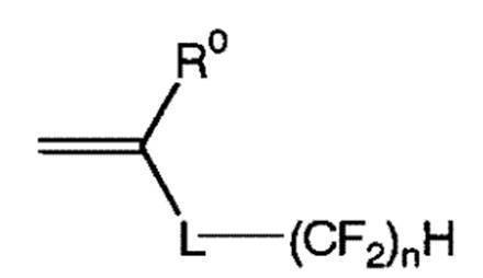
R0は、水素原子、ハロゲン原子、または、メチル基を表す。
Lは、2価の連結基を表す。Lとしては、炭素数2~16のアルキレン基が好ましく、上記アルキレン基において隣接しない任意の-CH2-は、-O-、-COO-、-CO-、または、-CONH-に置換されていてもよい。
nは、1~18の整数を表す。
Lは、2価の連結基を表す。Lとしては、炭素数2~16のアルキレン基が好ましく、上記アルキレン基において隣接しない任意の-CH2-は、-O-、-COO-、-CO-、または、-CONH-に置換されていてもよい。
nは、1~18の整数を表す。
式(40)で表される化合物由来の繰り返し単位を有するレベリング剤は、さらに他の繰り返し単位を含んでいてもよい。
他の繰り返し単位としては、式(41)で表される化合物由来の繰り返し単位が挙げられる。
他の繰り返し単位としては、式(41)で表される化合物由来の繰り返し単位が挙げられる。
式(41)

R11は、水素原子、ハロゲン原子、または、メチル基を表す。
Xは、酸素原子、硫黄原子、または、-N(R13)-を表す。R13は、水素原子、または、炭素数1~8のアルキル基を表す。
R12は、水素原子、置換基を有してもよいアルキル基、または、置換基を有していてもよい芳香族基を表す。上記アルキル基の炭素数は、1~20が好ましい。上記アルキル基は、直鎖状、分岐鎖状、および、環状のいずれであってもよい。
また、上記アルキル基の有していてもよい置換基としては、ポリ(アルキレンオキシ)基、および、重合性基が挙げられる。重合性基の例は、上述した通りである。
Xは、酸素原子、硫黄原子、または、-N(R13)-を表す。R13は、水素原子、または、炭素数1~8のアルキル基を表す。
R12は、水素原子、置換基を有してもよいアルキル基、または、置換基を有していてもよい芳香族基を表す。上記アルキル基の炭素数は、1~20が好ましい。上記アルキル基は、直鎖状、分岐鎖状、および、環状のいずれであってもよい。
また、上記アルキル基の有していてもよい置換基としては、ポリ(アルキレンオキシ)基、および、重合性基が挙げられる。重合性基の例は、上述した通りである。
レベリング剤が、式(40)で表される化合物由来の繰り返し単位、および、式(41)で表される化合物由来の繰り返し単位を含む場合、式(40)で表される化合物由来の繰り返し単位の含有量は、レベリング剤が含む全繰り返し単位に対して、10~95モル%が好ましく、15~90モル%がより好ましい。
レベリング剤が、式(40)で表される化合物由来の繰り返し単位、および、式(41)で表される化合物由来の繰り返し単位を含む場合、式(41)で表される化合物由来の繰り返し単位の含有量は、レベリング剤が含む全繰り返し単位に対して、10~90モル%が好ましく、20~80モル%がより好ましい。
レベリング剤が、式(40)で表される化合物由来の繰り返し単位、および、式(41)で表される化合物由来の繰り返し単位を含む場合、式(41)で表される化合物由来の繰り返し単位の含有量は、レベリング剤が含む全繰り返し単位に対して、10~90モル%が好ましく、20~80モル%がより好ましい。
また、レベリング剤としては、上述した式(40)で表される化合物由来の繰り返し単位に代えて、式(42)で表される化合物由来の繰り返し単位を含むレベリング剤も挙げられる。
式(42)

R2は、水素原子、ハロゲン原子、または、メチル基を表す。
L2は、2価の連結基を表す。
nは、1~18の整数を表す。
L2は、2価の連結基を表す。
nは、1~18の整数を表す。
レベリング剤の具体例としては、特開2004-331812号公報の段落0046~0052に例示される化合物、および、特開2008-257205号公報の段落0038~0052に記載の化合物が挙げられる。
組成物中のレベリング剤の含有量は、液晶性化合物全質量に対して、0.001~10質量%が好ましく、0.01~5質量%がより好ましい。
レベリング剤は、単独で用いてもよいし、2種以上を組み合わせて用いてもよい。レベリング剤が2種以上を用いられる場合、それらの合計量が上記範囲であることが好ましい。
レベリング剤は、単独で用いてもよいし、2種以上を組み合わせて用いてもよい。レベリング剤が2種以上を用いられる場合、それらの合計量が上記範囲であることが好ましい。
(重合性成分)
光吸収異方性層形成用組成物は、重合性成分を含むことが好ましい。
重合性成分としては、例えば、アクリレートを含む化合物(例えば、アクリレートモノマー)が挙げられる。この場合、本発明における光吸収異方性層は、上記アクリレートを含む化合物を重合させて得られるポリアクリレートを含む。具体的には、特開2017-122776号公報の段落0058に記載の化合物が挙げられる。
光吸収異方性層形成用組成物が重合性成分を含む場合、重合性成分の含有量は、光吸収異方性層形成用組成物中の上記二色性物質と上記液晶性化合物との合計100質量部に対し、3~20質量部が好ましい。
光吸収異方性層形成用組成物は、重合性成分を含むことが好ましい。
重合性成分としては、例えば、アクリレートを含む化合物(例えば、アクリレートモノマー)が挙げられる。この場合、本発明における光吸収異方性層は、上記アクリレートを含む化合物を重合させて得られるポリアクリレートを含む。具体的には、特開2017-122776号公報の段落0058に記載の化合物が挙げられる。
光吸収異方性層形成用組成物が重合性成分を含む場合、重合性成分の含有量は、光吸収異方性層形成用組成物中の上記二色性物質と上記液晶性化合物との合計100質量部に対し、3~20質量部が好ましい。
(重合開始剤)
光吸収異方性層形成用組成物は、重合開始剤を含むことが好ましい。
重合開始剤としては特に制限はないが、感光性を有する化合物、すなわち光重合開始剤であることが好ましい。
光重合開始剤としては、各種の化合物を特に制限なく使用できる。光重合開始剤の例には、α-カルボニル化合物(米国特許第2367661号、同2367670号の各明細書)、アシロインエーテル(米国特許第2448828号明細書)、α-炭化水素置換芳香族アシロイン化合物(米国特許第2722512号明細書)、多核キノン化合物(米国特許第3046127号および同2951758号の各明細書)、トリアリールイミダゾールダイマーとp-アミノフェニルケトンとの組み合わせ(米国特許第3549367号明細書)、アクリジンおよびフェナジン化合物(特開昭60-105667号公報および米国特許第4239850号明細書)、オキサジアゾール化合物(米国特許第4212970号明細書)、o-アシルオキシム化合物(特開2016-27384明細書[0065])、および、アシルフォスフィンオキシド化合物(特公昭63-40799号公報、特公平5-29234号公報、特開平10-95788号公報、および、特開平10-29997号公報)等が挙げられる。
このような光重合開始剤としては、市販品も用いることができ、BASF社製のIRGACURE 184、IRGACURE 907、IRGACURE 369、IRGACURE 651、IRGACURE 819、IRGACURE 2959、IRGACURE OXE-01、および、IRGACURE OXE-02等が挙げられる。
光吸収異方性層形成用組成物は、重合開始剤を含むことが好ましい。
重合開始剤としては特に制限はないが、感光性を有する化合物、すなわち光重合開始剤であることが好ましい。
光重合開始剤としては、各種の化合物を特に制限なく使用できる。光重合開始剤の例には、α-カルボニル化合物(米国特許第2367661号、同2367670号の各明細書)、アシロインエーテル(米国特許第2448828号明細書)、α-炭化水素置換芳香族アシロイン化合物(米国特許第2722512号明細書)、多核キノン化合物(米国特許第3046127号および同2951758号の各明細書)、トリアリールイミダゾールダイマーとp-アミノフェニルケトンとの組み合わせ(米国特許第3549367号明細書)、アクリジンおよびフェナジン化合物(特開昭60-105667号公報および米国特許第4239850号明細書)、オキサジアゾール化合物(米国特許第4212970号明細書)、o-アシルオキシム化合物(特開2016-27384明細書[0065])、および、アシルフォスフィンオキシド化合物(特公昭63-40799号公報、特公平5-29234号公報、特開平10-95788号公報、および、特開平10-29997号公報)等が挙げられる。
このような光重合開始剤としては、市販品も用いることができ、BASF社製のIRGACURE 184、IRGACURE 907、IRGACURE 369、IRGACURE 651、IRGACURE 819、IRGACURE 2959、IRGACURE OXE-01、および、IRGACURE OXE-02等が挙げられる。
光吸収異方性層形成用組成物が重合開始剤を含有する場合、重合開始剤の含有量は、光吸収異方性層形成用組成物中の上記二色性物質と上記高分子液晶性化合物との合計100質量部に対し、0.01~30質量部が好ましく、0.1~15質量部がより好ましい。重合開始剤の含有量が0.01質量部以上であることで、光吸収異方性膜の耐久性が良好となり、30質量部以下であることで、光吸収異方性層における二色性物質の配向度がより良好となる。
重合開始剤は、1種単独で用いても2種以上を併用してもよい。重合開始剤を2種以上含む場合、その合計量が上記範囲内であるのが好ましい。
重合開始剤は、1種単独で用いても2種以上を併用してもよい。重合開始剤を2種以上含む場合、その合計量が上記範囲内であるのが好ましい。
(二色性物質の含有量)
二色性物質の含有量は、光吸収異方性層の全固形分質量に対して、10~30質量%が好ましく、15~30質量%がより好ましく、18~28質量%がさらに好ましく、20~26質量%が特に好ましい。全固形分質量とは、光吸収異方性層形成用組成物の質量から、溶剤成分を除いた質量を意味する。
二色性物質の含有量が上記範囲内にあれば、光吸収異方性層を薄膜にした場合であっても、高配向度の光吸収異方性層を得ることができる。そのため、フレキシブル性に優れた光吸収異方性層が得られやすい。
第1の二色性アゾ色素化合物の含有量は、二色性物質全体の含有量100質量部に対して、40~90質量部が好ましく、45~75質量部がより好ましい。
第2の二色性アゾ色素化合物の含有量は、二色性物質全体の含有量100質量に対して、6~50質量部が好ましく、8~35質量部がより好ましい。
第3の二色性アゾ色素化合物の含有量は、二色性アゾ色素化合物の含有量100質量に対して、3~50質量部が好ましく、5~40質量部がより好ましい。
第1の二色性アゾ色素化合物と、第2の二色性アゾ色素化合物と、および必要に応じて用いられる第3の二色性アゾ色素化合物と、の含有比は、光吸収異方性層の色味調整するために、任意に設定することができる。ただし、第1の二色性アゾ色素化合物に対する第2の二色性アゾ色素化合物の含有比(第2の二色性アゾ色素化合物/第1の二色性アゾ色素化合物)は、モル換算で、0.1~10が好ましく、0.2~5がより好ましく、0.3~0.8がさらに好ましい。第1の二色性アゾ色素化合物に対する第2の二色性アゾ色素化合物の含有比が上記範囲内にあれば、配向度が高められる。
二色性物質の含有量は、光吸収異方性層の全固形分質量に対して、10~30質量%が好ましく、15~30質量%がより好ましく、18~28質量%がさらに好ましく、20~26質量%が特に好ましい。全固形分質量とは、光吸収異方性層形成用組成物の質量から、溶剤成分を除いた質量を意味する。
二色性物質の含有量が上記範囲内にあれば、光吸収異方性層を薄膜にした場合であっても、高配向度の光吸収異方性層を得ることができる。そのため、フレキシブル性に優れた光吸収異方性層が得られやすい。
第1の二色性アゾ色素化合物の含有量は、二色性物質全体の含有量100質量部に対して、40~90質量部が好ましく、45~75質量部がより好ましい。
第2の二色性アゾ色素化合物の含有量は、二色性物質全体の含有量100質量に対して、6~50質量部が好ましく、8~35質量部がより好ましい。
第3の二色性アゾ色素化合物の含有量は、二色性アゾ色素化合物の含有量100質量に対して、3~50質量部が好ましく、5~40質量部がより好ましい。
第1の二色性アゾ色素化合物と、第2の二色性アゾ色素化合物と、および必要に応じて用いられる第3の二色性アゾ色素化合物と、の含有比は、光吸収異方性層の色味調整するために、任意に設定することができる。ただし、第1の二色性アゾ色素化合物に対する第2の二色性アゾ色素化合物の含有比(第2の二色性アゾ色素化合物/第1の二色性アゾ色素化合物)は、モル換算で、0.1~10が好ましく、0.2~5がより好ましく、0.3~0.8がさらに好ましい。第1の二色性アゾ色素化合物に対する第2の二色性アゾ色素化合物の含有比が上記範囲内にあれば、配向度が高められる。
[光吸収異方性層の性状]
本発明の光吸収異方性層は、透過率中心軸から30°傾けた透過率(以下、特段の断りがない限り波長550nmにおける透過率を示す。)が60%以下であることが好ましく、40%以下であることがより好ましく、20%以下であることがさらに好ましい。これにより、透過率中心と透過率中心からずれた方向の照度のコントラストを高めることが可能となり、視角を十分に狭くすることができる。
本発明の光吸収異方性層は、透過率中心軸から30°傾けた透過率(以下、特段の断りがない限り波長550nmにおける透過率を示す。)が60%以下であることが好ましく、40%以下であることがより好ましく、20%以下であることがさらに好ましい。これにより、透過率中心と透過率中心からずれた方向の照度のコントラストを高めることが可能となり、視角を十分に狭くすることができる。
本発明に用いられる光吸収異方性層の透過率中心軸の透過率は、65%以上が好ましく、75%以上がより好ましく、85%以上がさらに好ましい。上限は特に制限されないが、100%未満が挙げられる。透過率が上記範囲であると、光吸収異方性層を用いた画像表示装置の視角中心の照度を上げ、視認性を良好とすることができる。
本発明の液晶表示装置において、視野角中心の照度をなるべく下げないようにしつつ周辺部の照度をなるべく下げることを達成するためには、光吸収異方性層の波長550nmで測定される配向度が、0.80以上が好ましく、0.90以上がより好ましく、0.95以上がさらに好ましい。
なお、ここで、波長λnmで測定される配向度とは、本明細書において以下の定義に従うものとする。
AxoScan OPMF-1(オプトサイエンス社製)を用いて、測定の際に、光吸収異方性層の法線方向に対する角度である極角を0~90°まで5°毎に変更しつつ、各極角における波長550nmでのミュラーマトリックスを実測し、最小透過率(Tmin)を導出する。次に、表面反射の影響を除去した後、Tminが最も高くなる極角におけるTminをTm(0)、Tminの最も高い極角からさらに40°極角を大きくした方向のTminをTm(40)とする。得られたTm(0)およびTm(40)から下記式により吸光度を算出し、A(0)およびA(40)を算出する。
A=-log(Tm)
ここで、Tmは透過率、Aは吸光度を表す。
算出したA(0)およびA(40)より、下記式で定義された波長550nmにおける配向度Sを算出する。
S=(4.6×A(40)-A(0))/(4.6×A(40)+2×A(0))
上記波長を550nmから420nmまたは650nmに変更することにより、波長420nmおよび650nmおける配向度Sを算出する。
なお、ここで、波長λnmで測定される配向度とは、本明細書において以下の定義に従うものとする。
AxoScan OPMF-1(オプトサイエンス社製)を用いて、測定の際に、光吸収異方性層の法線方向に対する角度である極角を0~90°まで5°毎に変更しつつ、各極角における波長550nmでのミュラーマトリックスを実測し、最小透過率(Tmin)を導出する。次に、表面反射の影響を除去した後、Tminが最も高くなる極角におけるTminをTm(0)、Tminの最も高い極角からさらに40°極角を大きくした方向のTminをTm(40)とする。得られたTm(0)およびTm(40)から下記式により吸光度を算出し、A(0)およびA(40)を算出する。
A=-log(Tm)
ここで、Tmは透過率、Aは吸光度を表す。
算出したA(0)およびA(40)より、下記式で定義された波長550nmにおける配向度Sを算出する。
S=(4.6×A(40)-A(0))/(4.6×A(40)+2×A(0))
上記波長を550nmから420nmまたは650nmに変更することにより、波長420nmおよび650nmおける配向度Sを算出する。
本発明の光吸収異方性層を用いた光学フィルムは、透過率中心軸の透過率が高く、透過率中心軸からずれた方向の透過率を低くすることができる。これは、以下の理由によると推定される。
透過率中心軸からずれた方向の透過率を低くするためには、光吸収異方性層の厚みを増やすことで実現し得るが、同時に透過率中心軸の透過率を低下させる。ここで、波長550nmで測定される配向度を0.95以上にすると、波長550nmで測定される配向度に寄与しているのは主に二色性物質であると考えられるため、二色性物質の吸収軸が透過率中心軸からずれたものの存在頻度が下がると考えられる。それにより、透過率中心軸から見た時の二色性物質による吸収を抑制できた結果、透過率中心軸方向の透過率を高くできたと推定できる。
透過率中心軸からずれた方向の透過率を低くするためには、光吸収異方性層の厚みを増やすことで実現し得るが、同時に透過率中心軸の透過率を低下させる。ここで、波長550nmで測定される配向度を0.95以上にすると、波長550nmで測定される配向度に寄与しているのは主に二色性物質であると考えられるため、二色性物質の吸収軸が透過率中心軸からずれたものの存在頻度が下がると考えられる。それにより、透過率中心軸から見た時の二色性物質による吸収を抑制できた結果、透過率中心軸方向の透過率を高くできたと推定できる。
また、光吸収異方性層が下記式(1)および式(2)をともに満たすことが好ましい。
SP(420nm)<SP(550nm) 式(1)
SP(420nm)<SP(650nm) 式(2)
ここで、上記SP(λ)は、波長λnmで測定される、光吸収異方性層の配向度を表す。
SP(420nm)<SP(550nm) 式(1)
SP(420nm)<SP(650nm) 式(2)
ここで、上記SP(λ)は、波長λnmで測定される、光吸収異方性層の配向度を表す。
光吸収異方性層の厚さは、特に限定されないが、後述する本発明の光学積層体を偏光素子に用いた場合のフレキシブル性の点で、100~8000nmであることが好ましく、300~5000nmであることがより好ましい。
[光吸収異方性層の形成方法]
光吸収異方性層の形成方法は特に限定されず、上述した光吸収異方性層形成用組成物を塗布して塗布膜を形成する工程(以下、「塗布膜形成工程」ともいう。)と、塗布膜に含まれる液晶性成分や二色性物質を配向させる工程(以下、「配向工程」ともいう。)と、をこの順に含む方法が挙げられる。
なお、液晶性成分とは、上述した液晶性化合物だけでなく、上述した二色性物質が液晶性を有している場合は、液晶性を有する二色性物質も含む成分である。
光吸収異方性層の形成方法は特に限定されず、上述した光吸収異方性層形成用組成物を塗布して塗布膜を形成する工程(以下、「塗布膜形成工程」ともいう。)と、塗布膜に含まれる液晶性成分や二色性物質を配向させる工程(以下、「配向工程」ともいう。)と、をこの順に含む方法が挙げられる。
なお、液晶性成分とは、上述した液晶性化合物だけでなく、上述した二色性物質が液晶性を有している場合は、液晶性を有する二色性物質も含む成分である。
なお、有機二色性色素を所望の配向とする技術は、有機二色性色素を利用した偏光子の作製技術や、ゲスト-ホスト液晶セルの作製技術などを参考にすることができる。例えば、特開平11-305036公報や特開2002-90526号公報に記載の二色性偏光素子の作製方法、および特開2002-99388号公報や特開2016-27387公報に記載のゲストホスト型液晶表示装置の作製方法で利用されている技術を、本発明に用いられる光吸収異方性層の作製にも利用することができる。
例えば、ゲストホスト型液晶セルの技術を利用して、ホスト液晶の配向に付随させて有機二色性色素の分子を、上記のような所望の配向にすることができる。具体的には、ゲストとなる有機二色性色素と、ホスト液晶となる棒状液晶性化合物とを混合し、ホスト液晶を配向させるとともに、その液晶分子の配向に沿って有機二色性色素の分子を配向させて、その配向状態を固定することで、本発明に用いられる光吸収異方性層を作製することができる。
本発明に用いられる光吸収異方性層の光吸収特性の使用環境による変動を防止するために、有機二色性色素の配向を、化学結合の形成によって固定するのが好ましい。例えば、ホスト液晶、有機二色性色素、または所望により添加される重合性成分の重合を進行させることで、配向を固定することができる。
また、一対の基板に、有機二色性色素とホスト液晶とを少なくとも含む液晶層を有するゲストホスト型液晶セルそのものを、本発明に用いられる光吸収異方性層として利用してもよい。ホスト液晶の配向(およびそれに付随する有機二色性色素分子の配向)は、基板内面に形成された配向膜によって制御することができ、電界等の外部刺激を与えない限り、その配向状態は維持され、本発明に用いられる光吸収異方性層の光吸収特性を一定にすることができる。
また、ポリマーフィルム中に有機二色性色素を浸透させて、ポリマーフィルム中のポリマー分子の配向に沿って有機二色性色素を配向させることで、本発明に用いられる光吸収異方性層に要求される光吸収特性を満足するポリマーフィルムを作製することができる。具体的には、有機二色性色素の溶液をポリマーフィルムの表面に塗布して、フィルム中に浸透させて、作製することができる。有機二色性色素の配向は、ポリマーフィルム中のポリマー鎖の配向、その性質(ポリマー鎖またはそれが有する官能基等の化学的および物理的性質)、塗布方法、などによって調整することができる。この方法の詳細については、特開2002-90526号公報に記載されている。
以下、塗布膜形成工程、配向工程、および、他の工程について以下に説明する。
(塗布膜形成工程)
塗布膜形成工程は、光吸収異方性層形成用組成物を塗布して塗布膜を形成する工程である。
上述した溶媒を含有する光吸収異方性層形成用組成物を用いたり、光吸収異方性層形成用組成物を加熱等によって溶融液等の液状物としたものを用いたりすることにより、光吸収異方性層形成用組成物を塗布することが容易になる。
光吸収異方性層形成用組成物の塗布方法としては、例えば、ロールコーティング法、グラビア印刷法、スピンコート法、ワイヤーバーコーティング法、押し出しコーティング法、ダイレクトグラビアコーティング法、リバースグラビアコーティング法、ダイコーティング法、スプレー法、および、インクジェット法等の公知の方法が挙げられる。
塗布膜形成工程は、光吸収異方性層形成用組成物を塗布して塗布膜を形成する工程である。
上述した溶媒を含有する光吸収異方性層形成用組成物を用いたり、光吸収異方性層形成用組成物を加熱等によって溶融液等の液状物としたものを用いたりすることにより、光吸収異方性層形成用組成物を塗布することが容易になる。
光吸収異方性層形成用組成物の塗布方法としては、例えば、ロールコーティング法、グラビア印刷法、スピンコート法、ワイヤーバーコーティング法、押し出しコーティング法、ダイレクトグラビアコーティング法、リバースグラビアコーティング法、ダイコーティング法、スプレー法、および、インクジェット法等の公知の方法が挙げられる。
(配向工程)
配向工程は、塗布膜に含まれる液晶性成分を配向させる工程である。これにより、光吸収異方性層が得られる。配向工程は、乾燥処理、加熱処理、および、冷却処理を有していてもよい。以下、上記各処理について説明する。
配向工程は、乾燥処理を有していてもよい。乾燥処理によって、溶媒等の成分を塗布膜から除去することができる。乾燥処理は、塗布膜を室温下において所定時間放置する方法(例えば、自然乾燥)によって行われてもよいし、加熱および/または送風する方法によって行われてもよい。
ここで、光吸収異方性層形成用組成物に含まれる液晶性成分は、上述した塗布膜形成工程または乾燥処理によって、配向する場合がある。例えば、光吸収異方性層形成用組成物が溶媒を含む塗布液として調製されている態様では、塗布膜を乾燥して、塗布膜から溶媒を除去することで、光吸収異方性を持つ塗布膜(すなわち、光吸収異方性膜)が得られる。
乾燥処理が塗布膜に含まれる液晶性成分の液晶相への転移温度以上の温度により行われる場合には、後述する加熱処理は実施しなくてもよい。
配向工程は、塗布膜に含まれる液晶性成分を配向させる工程である。これにより、光吸収異方性層が得られる。配向工程は、乾燥処理、加熱処理、および、冷却処理を有していてもよい。以下、上記各処理について説明する。
配向工程は、乾燥処理を有していてもよい。乾燥処理によって、溶媒等の成分を塗布膜から除去することができる。乾燥処理は、塗布膜を室温下において所定時間放置する方法(例えば、自然乾燥)によって行われてもよいし、加熱および/または送風する方法によって行われてもよい。
ここで、光吸収異方性層形成用組成物に含まれる液晶性成分は、上述した塗布膜形成工程または乾燥処理によって、配向する場合がある。例えば、光吸収異方性層形成用組成物が溶媒を含む塗布液として調製されている態様では、塗布膜を乾燥して、塗布膜から溶媒を除去することで、光吸収異方性を持つ塗布膜(すなわち、光吸収異方性膜)が得られる。
乾燥処理が塗布膜に含まれる液晶性成分の液晶相への転移温度以上の温度により行われる場合には、後述する加熱処理は実施しなくてもよい。
塗布膜に含まれる液晶性成分の液晶相への転移温度は、製造適性等の面から10~250℃が好ましく、25~190℃がより好ましい。上記転移温度が10℃以上であると、液晶相を呈する温度範囲にまで温度を下げるための冷却処理等が必要とならず、好ましい。また、上記転移温度が250℃以下であると、一旦液晶相を呈する温度範囲よりもさらに高温の等方性液体状態にする場合にも高温を要さず、熱エネルギーの浪費、ならびに、基板の変形および変質等を低減できるため、好ましい。
配向工程は、加熱処理を有することが好ましい。これにより、塗布膜に含まれる液晶性成分を配向させることができるため、加熱処理後の塗布膜を光吸収異方性膜として好適に使用できる。
加熱処理は、製造適性等の面から10~250℃が好ましく、25~190℃がより好ましい。また、加熱時間は、1~300秒が好ましく、1~60秒がより好ましい。
加熱処理は、製造適性等の面から10~250℃が好ましく、25~190℃がより好ましい。また、加熱時間は、1~300秒が好ましく、1~60秒がより好ましい。
配向工程は、加熱処理後に実施される冷却処理を有していてもよい。冷却処理は、加熱後の塗布膜を室温(20~25℃)程度まで冷却する処理である。これにより、塗布膜に含まれる液晶性成分の配向を固定することができる。冷却手段としては、特に限定されず、公知の方法により実施できる。
以上の工程によって、光吸収異方性膜を得ることができる。
なお、本態様では、塗布膜に含まれる液晶性成分を配向する方法として、乾燥処理および加熱処理等を挙げているが、これに限定されず、公知の配向処理によって実施できる。
以上の工程によって、光吸収異方性膜を得ることができる。
なお、本態様では、塗布膜に含まれる液晶性成分を配向する方法として、乾燥処理および加熱処理等を挙げているが、これに限定されず、公知の配向処理によって実施できる。
(他の工程)
光吸収異方性層の形成方法は、上記配向工程後に、光吸収異方性層を硬化させる工程(以下、「硬化工程」ともいう。)を有していてもよい。
硬化工程は、例えば、光吸収異方性層が架橋性基(重合性基)を有している場合には、加熱および/または光照射(露光)によって実施される。このなかでも、硬化工程は光照射によって実施されることが好ましい。
硬化に用いる光源は、赤外線、可視光または紫外線等、種々の光源を用いることが可能であるが、紫外線であることが好ましい。また、硬化時に加熱しながら紫外線を照射してもよいし、特定の波長のみを透過するフィルターを介して紫外線を照射してもよい。
露光が加熱しながら行われる場合、露光時の加熱温度は、液晶膜に含まれる液晶性成分の液晶相への転移温度にもよるが、25~140℃であることが好ましい。
また、露光は、窒素雰囲気下で行われてもよい。ラジカル重合によって液晶膜の硬化が進行する場合において、酸素による重合の阻害が低減されるため、窒素雰囲気下で露光することが好ましい。
光吸収異方性層の形成方法は、上記配向工程後に、光吸収異方性層を硬化させる工程(以下、「硬化工程」ともいう。)を有していてもよい。
硬化工程は、例えば、光吸収異方性層が架橋性基(重合性基)を有している場合には、加熱および/または光照射(露光)によって実施される。このなかでも、硬化工程は光照射によって実施されることが好ましい。
硬化に用いる光源は、赤外線、可視光または紫外線等、種々の光源を用いることが可能であるが、紫外線であることが好ましい。また、硬化時に加熱しながら紫外線を照射してもよいし、特定の波長のみを透過するフィルターを介して紫外線を照射してもよい。
露光が加熱しながら行われる場合、露光時の加熱温度は、液晶膜に含まれる液晶性成分の液晶相への転移温度にもよるが、25~140℃であることが好ましい。
また、露光は、窒素雰囲気下で行われてもよい。ラジカル重合によって液晶膜の硬化が進行する場合において、酸素による重合の阻害が低減されるため、窒素雰囲気下で露光することが好ましい。
光吸収異方性層の厚さは、特に限定されないが、後述する本発明の積層体を偏光素子に用いた場合のフレキシブル性の観点から、100~8000nmであることが好ましく、300~5000nmであることがより好ましい。
(光吸収異方性層のパターニング)
また、本発明の光吸収異方性層は、面内に領域Aと領域Bを有し、領域Aと領域Bの極角30°から見た斜め透過率(以下、極角30°透過率とする)が異なる、光吸収異方性層であることが可能である。この場合、領域Aの極角30°透過率が10%以下であり、領域Bの極角30°透過率が80%以上である、光吸収異方性層であることが好ましい。
上記のような領域は、パターニングを行うことで、視野角依存性を強めたり弱めたりすることが可能となる。これにより、視野角依存性を強めた領域にのみ機密度の高い情報を表示したりすることもできる。また、表示装置として視野角依存性を自在に制御することにより、意匠性に優れた設計も可能となる。μLED等の表示装置において発光部から周辺領域への光漏れを防止するために、発光部以外の領域を極角30°透過率が高い領域にし、発光部を極角30°透過率が低い領域とするパターニングにすることで画面の中の明暗のコントラストを高めることも可能である。
また、本発明の光吸収異方性層は、面内に領域Aと領域Bを有し、領域Aと領域Bの極角30°から見た斜め透過率(以下、極角30°透過率とする)が異なる、光吸収異方性層であることが可能である。この場合、領域Aの極角30°透過率が10%以下であり、領域Bの極角30°透過率が80%以上である、光吸収異方性層であることが好ましい。
上記のような領域は、パターニングを行うことで、視野角依存性を強めたり弱めたりすることが可能となる。これにより、視野角依存性を強めた領域にのみ機密度の高い情報を表示したりすることもできる。また、表示装置として視野角依存性を自在に制御することにより、意匠性に優れた設計も可能となる。μLED等の表示装置において発光部から周辺領域への光漏れを防止するために、発光部以外の領域を極角30°透過率が高い領域にし、発光部を極角30°透過率が低い領域とするパターニングにすることで画面の中の明暗のコントラストを高めることも可能である。
-パターン形成方法-
このように面内で異なる2つ以上の領域を有するパターン光吸収異方性層の形成方法には、特に制限されず、WO2019/176918号公報に記載されているような公知の各種の方法が利用可能である。一例として、パターン光吸収異方性層の厚さを面内で制御する方法、パターン光吸収異方性層中の二色性色素化合物を偏在させる方法、および、光学的に均一なパターン光吸収異方性層を後加工する方法等が挙げられる。
パターン光吸収異方性層の厚さを面内で制御する方法としては、リソグラフィを利用する方法、インプリントを利用する方法、および、凹凸構造を有する基材にパターン光吸収異方性層を形成する方法等が挙げられる。パターン光吸収異方性層中の二色性色素化合物を偏在させる方法としては、溶剤浸漬により二色性色素化合物を抽出する方法(ブリーチング)が挙げられる。さらに、光学的に均一なパターン光吸収異方性層を後加工する方法としては、レーザー加工等によって、平坦な光吸収異方性層の一部を裁断する方法が挙げられる。
このように面内で異なる2つ以上の領域を有するパターン光吸収異方性層の形成方法には、特に制限されず、WO2019/176918号公報に記載されているような公知の各種の方法が利用可能である。一例として、パターン光吸収異方性層の厚さを面内で制御する方法、パターン光吸収異方性層中の二色性色素化合物を偏在させる方法、および、光学的に均一なパターン光吸収異方性層を後加工する方法等が挙げられる。
パターン光吸収異方性層の厚さを面内で制御する方法としては、リソグラフィを利用する方法、インプリントを利用する方法、および、凹凸構造を有する基材にパターン光吸収異方性層を形成する方法等が挙げられる。パターン光吸収異方性層中の二色性色素化合物を偏在させる方法としては、溶剤浸漬により二色性色素化合物を抽出する方法(ブリーチング)が挙げられる。さらに、光学的に均一なパターン光吸収異方性層を後加工する方法としては、レーザー加工等によって、平坦な光吸収異方性層の一部を裁断する方法が挙げられる。
[色味調整層]
本発明の光学フィルムは、少なくとも1種の有機色素化合物を含む色味調整層を有する。
以下、色味調整層によって広角色味抑制性に優れる光学フィルムが得られる説明(色味調整の原理)、色味調整層が含む有機色素化合物、および、色味調整層の性状について詳述する。
本発明の光学フィルムは、少なくとも1種の有機色素化合物を含む色味調整層を有する。
以下、色味調整層によって広角色味抑制性に優れる光学フィルムが得られる説明(色味調整の原理)、色味調整層が含む有機色素化合物、および、色味調整層の性状について詳述する。
(色味調整の原理)
二色性物質を含む光学フィルムの色味制御は、通常、フィルムに含まれる二色性物質の添加量および/または添加量比を調整することで行う。しかし、波長によって算出される配向度が変化する場合、広角色味抑制性に優れる光学フィルムを得るためには、二色性物質の添加量および/または添加量比の調整だけでは困難である。
例えば、上記チエノチアゾール骨格を有する二色性物質を用いる際、複数の方向に対して異なる吸収波長を有することがあり、その二色性物質の主吸収波長範囲外の波長で測定される配向度を低下させてしまうという問題が発生し得る。
具体的には、例えば、チエノチアゾール骨格を有する二色性色素化合物を光吸収異方性層に用いた場合、短波長域で測定される配向度が低下してしまい、各波長で測定される配向度をS(λ)としたとき、上記式(1)および式(2)の関係を満たしやすくなる。
式(1)および式(2)の関係を満たすとき、SP(420nm)がSP(550nm)およびSP(650nm)よりも小さいため、見かけ上、短波長域のみの配向度が低い状態となる。このとき、例えば、複数の二色性物質を配合し、透過率中心軸方向から見た場合の色味をニュートラルにしたとしても、斜め方向から見た場合の色味はニュートラルにならない。つまり、式(1)、および、式(2)の関係を満たすとき、光学フィルム中の二色性物質の添加量および/または添加量比の調整だけでは、広角色味抑制性に優れる光学フィルムを得ることは困難である。
二色性物質を含む光学フィルムの色味制御は、通常、フィルムに含まれる二色性物質の添加量および/または添加量比を調整することで行う。しかし、波長によって算出される配向度が変化する場合、広角色味抑制性に優れる光学フィルムを得るためには、二色性物質の添加量および/または添加量比の調整だけでは困難である。
例えば、上記チエノチアゾール骨格を有する二色性物質を用いる際、複数の方向に対して異なる吸収波長を有することがあり、その二色性物質の主吸収波長範囲外の波長で測定される配向度を低下させてしまうという問題が発生し得る。
具体的には、例えば、チエノチアゾール骨格を有する二色性色素化合物を光吸収異方性層に用いた場合、短波長域で測定される配向度が低下してしまい、各波長で測定される配向度をS(λ)としたとき、上記式(1)および式(2)の関係を満たしやすくなる。
式(1)および式(2)の関係を満たすとき、SP(420nm)がSP(550nm)およびSP(650nm)よりも小さいため、見かけ上、短波長域のみの配向度が低い状態となる。このとき、例えば、複数の二色性物質を配合し、透過率中心軸方向から見た場合の色味をニュートラルにしたとしても、斜め方向から見た場合の色味はニュートラルにならない。つまり、式(1)、および、式(2)の関係を満たすとき、光学フィルム中の二色性物質の添加量および/または添加量比の調整だけでは、広角色味抑制性に優れる光学フィルムを得ることは困難である。
また、複数の二色性物質が光学フィルムに含まれる場合、光学フィルム中における各二色性物質の配向のしやすさが異なっても、配向度を測定する波長によって算出される配向度が変化することがあり、光学フィルム中の二色性物質の添加量および/または添加量比の調整だけでは広角色味抑制性に優れる光学フィルムを得ることが困難である。
本発明においては、光吸収異方性層中の二色性物質の添加量および/または添加量比を調整して透過率中心軸方向の色味をニュートラルにした場合、透過率中心軸の斜め方向から見た色味の変化が大きくなりうる。ここで、二色性物質の添加量および/または添加量比を調整するとともに、下記要件1~3のいずれか1つを満たす色味調整層を用いて色味を調整することで、透過率中心軸方向、および、斜め方向からの見たときの色味変化を抑制することが容易となり、すなわち、広角色味抑制性がより良好な光学フィルムが得られると考えられる。
このとき、色味調整層が下記要件1~3のいずれか1つを満たすことで、色味調整層は透過率中心軸方向、および、斜め方向からの見たときの色味変化が小さく、光吸収異方性層の色味変化を相殺し、結果として広角色味抑制性がより良好な光学フィルムが得られると考えられる。
要件1:SC(420nm)<0.1
要件2:SC(550nm)<0.1
要件3:SC(650nm)<0.1
ただし、SC(λnm)は波長λnmで測定される、色味調整層の配向度を表す。
このとき、色味調整層が下記要件1~3のいずれか1つを満たすことで、色味調整層は透過率中心軸方向、および、斜め方向からの見たときの色味変化が小さく、光吸収異方性層の色味変化を相殺し、結果として広角色味抑制性がより良好な光学フィルムが得られると考えられる。
要件1:SC(420nm)<0.1
要件2:SC(550nm)<0.1
要件3:SC(650nm)<0.1
ただし、SC(λnm)は波長λnmで測定される、色味調整層の配向度を表す。
(色味調整層が含む有機色素化合物)
色味調整層は、少なくとも1種の有機色素化合物を含む。
色味調整層に含まれる色素化合物が有する構造として、例えば、アゾ構造、メチン構造、アントラキノン構造、トリアリールメタン構造、オキサジン構造、アゾメチン構造、フタロシアニン構造、ポルフィリン構造、ペリレン構造、ピロロピロール構造、および、スクアリリウム構造等が挙げられる。ここで、吸収波形、耐熱性、および、耐光性に優れる点で、メチン構造、アゾメチン構造、アゾ構造、フタロシアニン構造、および、アントラキノン構造が好ましく、アゾ構造、フタロシアニン構造、および、アントラキノン構造を有する化合物がより好ましく、アントラキノン構造を有する化合物がさらに好ましい。
上記構造を有する化合物の具体例としては、例えば、大川原信、松岡賢、平島恒亮、北尾悌次郎共著、機能性色素、講談社、1992年、および、時田澄男監修、エレクトロニクス関連材料、シーエムシー社、1998年に記載の色素化合物等が挙げられる。
色味調整層は、少なくとも1種の有機色素化合物を含む。
色味調整層に含まれる色素化合物が有する構造として、例えば、アゾ構造、メチン構造、アントラキノン構造、トリアリールメタン構造、オキサジン構造、アゾメチン構造、フタロシアニン構造、ポルフィリン構造、ペリレン構造、ピロロピロール構造、および、スクアリリウム構造等が挙げられる。ここで、吸収波形、耐熱性、および、耐光性に優れる点で、メチン構造、アゾメチン構造、アゾ構造、フタロシアニン構造、および、アントラキノン構造が好ましく、アゾ構造、フタロシアニン構造、および、アントラキノン構造を有する化合物がより好ましく、アントラキノン構造を有する化合物がさらに好ましい。
上記構造を有する化合物の具体例としては、例えば、大川原信、松岡賢、平島恒亮、北尾悌次郎共著、機能性色素、講談社、1992年、および、時田澄男監修、エレクトロニクス関連材料、シーエムシー社、1998年に記載の色素化合物等が挙げられる。
また、色味調整層に含まれる色素化合物が、ベンゼン環および複素環の少なくとも一方の構造を分子中に有することも好ましい。
ベンゼン環を有する構造としては、構造の一部にベンゼン環が含まれていればよい。ベンゼン環を有する構造としては、ベンゼン環、ナフタレン環、アントラセン環、フェナントレン環、フルオレン環、および、ピレン環、ならびに、アントラキノン構造、オキサジン構造、フタロシアニン構造、ポルフィリン構造、および、ペリレン構造が挙げられる。
複素環を有する構造としては、炭素以外のヘテロ原子を含む環状構造が挙げられる。複素環を有する構造は、芳香性を有していても有していなくてもよく、芳香性を有していることが好ましい。複素環を有する構造としては、ピロール環、フラン環、チオフェン環、イミダゾール環、ピラゾール環、オキサゾール環、ベンゾイミダゾール環、インドール環、プリン環、および、ベンゾトリアゾール環、ならびに、オキサジン構造、フタロシアニン構造、および、ポルフィリン構造が挙げられる。
ベンゼン環を有する構造としては、構造の一部にベンゼン環が含まれていればよい。ベンゼン環を有する構造としては、ベンゼン環、ナフタレン環、アントラセン環、フェナントレン環、フルオレン環、および、ピレン環、ならびに、アントラキノン構造、オキサジン構造、フタロシアニン構造、ポルフィリン構造、および、ペリレン構造が挙げられる。
複素環を有する構造としては、炭素以外のヘテロ原子を含む環状構造が挙げられる。複素環を有する構造は、芳香性を有していても有していなくてもよく、芳香性を有していることが好ましい。複素環を有する構造としては、ピロール環、フラン環、チオフェン環、イミダゾール環、ピラゾール環、オキサゾール環、ベンゾイミダゾール環、インドール環、プリン環、および、ベンゾトリアゾール環、ならびに、オキサジン構造、フタロシアニン構造、および、ポルフィリン構造が挙げられる。
本発明で用いられる色味調整層に含まれる色素化合物の吸収ピーク波長は500~650nmが好ましく、550~600nmがより好ましい。色素化合物の吸収ピーク波長をこの範囲に設定することで、本発明における光学フィルムの色味をよりニュートラルに調整することができる。
本明細書においては、色素化合物の吸収ピーク波長は、以下の方法で測定した吸収スペクトルにおける極大吸収波長をいう。
測定対象となる色素化合物1.0mgをクロロホルム100mlまたは水100mlに溶解させた溶液を調製する。
次いで、調製した溶液を、石英セル(1cm長四角セル)に入れ、紫外線可視赤外分光光度計U-3150(島津製作所)を用いて、溶液の波長領域200~800nmの範囲の吸光度を測定する。
次いで、得られた吸収スペクトルにおいて、極大吸収波長を求める。
測定対象となる色素化合物1.0mgをクロロホルム100mlまたは水100mlに溶解させた溶液を調製する。
次いで、調製した溶液を、石英セル(1cm長四角セル)に入れ、紫外線可視赤外分光光度計U-3150(島津製作所)を用いて、溶液の波長領域200~800nmの範囲の吸光度を測定する。
次いで、得られた吸収スペクトルにおいて、極大吸収波長を求める。
以下に、本発明に用いられる色素化合物の具体例を示すが、本発明はこれらに限定されるわけではない。
-アントラキノン構造を有する化合物-

-アゾ構造を有する化合物-
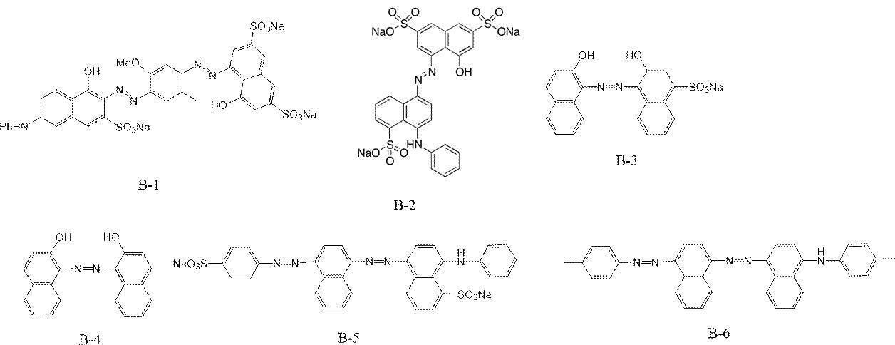
-トリアリールメタン構造を有する化合物-

-オキサジン構造を有する化合物-
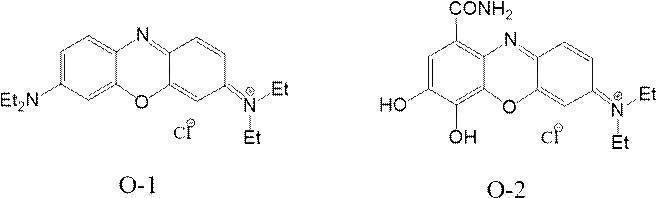
-フタロシアニン構造を有する化合物-
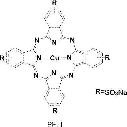
(色味調整層の性状)
また、色味調整層は下記要件1~3のいずれか1つを満たすことが好ましく、下記要件1~3のうち2つを満たすことがより好ましく、要件1~3の全てを満たすことがより好ましい。
要件1:SC(420nm)<0.1
要件2:SC(550nm)<0.1
要件3:SC(650nm)<0.1
なお、SC(λnm)は波長λnmで測定される、色味調整層の配向度を表す。波長λnmで測定される配向度は、上記光吸収異方性層の配向度の測定方法と同様であり、上記測定対象を色味調整層とすると得られる。
色味調整層を積層して光学フィルムを得る場合、転写積層前の色味調整層を測定に供してもよく、色味調整層を別の基材上に色味調整層を形成して測定に供してもよく、積層された光学フィルムから色味調整層を分離して測定に供してもよい。本明細書においては、積層された光学フィルムから色味調整層を分離したものを被測定物とした場合の配向度を記載する。
また、色味調整層は下記要件1~3のいずれか1つを満たすことが好ましく、下記要件1~3のうち2つを満たすことがより好ましく、要件1~3の全てを満たすことがより好ましい。
要件1:SC(420nm)<0.1
要件2:SC(550nm)<0.1
要件3:SC(650nm)<0.1
なお、SC(λnm)は波長λnmで測定される、色味調整層の配向度を表す。波長λnmで測定される配向度は、上記光吸収異方性層の配向度の測定方法と同様であり、上記測定対象を色味調整層とすると得られる。
色味調整層を積層して光学フィルムを得る場合、転写積層前の色味調整層を測定に供してもよく、色味調整層を別の基材上に色味調整層を形成して測定に供してもよく、積層された光学フィルムから色味調整層を分離して測定に供してもよい。本明細書においては、積層された光学フィルムから色味調整層を分離したものを被測定物とした場合の配向度を記載する。
色味調整層は、上記要件1~3のいずれか1つを満たすが、要件1~3全てを満たしてもよく、要件1~3から選ばれる2つを満たしてもよい。
また、色味調整層が満たす上記要件は、光吸収異方性層に含まれる二色性物質の配向度によって適宜選択されることが好ましい。以下、光吸収異方性層の配向度の関係と、その配向度の関係の場合に色味調整層が満たす好ましい要件の組合せを例示する。
例えば、下記「組合せ1:SP(420nm)<SP(650nm):要件3」は、光吸収異方性層が、上記第1の二色性アゾ色素化合物、および、上記第3の二色性アゾ色素化合物を含み、上記SP(420nm)が上記SP(650nm)よりも小さい場合、色味調整層は要件3を満たすことが好ましいことを意味する。
組合せ1:SP(420nm)<SP(650nm):要件3
組合せ2:SP(420nm)<SP(550nm):要件2
組合せ3:SP(550nm)<SP(420nm):要件1
組合せ4:SP(550nm)<SP(650nm):要件3
組合せ5:SP(650nm)<SP(420nm):要件1
組合せ6:SP(650nm)<SP(550nm):要件2
上記組合せのなかでも、組合せ1、2、5または6が好ましく、組合せ1または5がより好ましい。
また、色味調整層が満たす上記要件は、光吸収異方性層に含まれる二色性物質の配向度によって適宜選択されることが好ましい。以下、光吸収異方性層の配向度の関係と、その配向度の関係の場合に色味調整層が満たす好ましい要件の組合せを例示する。
例えば、下記「組合せ1:SP(420nm)<SP(650nm):要件3」は、光吸収異方性層が、上記第1の二色性アゾ色素化合物、および、上記第3の二色性アゾ色素化合物を含み、上記SP(420nm)が上記SP(650nm)よりも小さい場合、色味調整層は要件3を満たすことが好ましいことを意味する。
組合せ1:SP(420nm)<SP(650nm):要件3
組合せ2:SP(420nm)<SP(550nm):要件2
組合せ3:SP(550nm)<SP(420nm):要件1
組合せ4:SP(550nm)<SP(650nm):要件3
組合せ5:SP(650nm)<SP(420nm):要件1
組合せ6:SP(650nm)<SP(550nm):要件2
上記組合せのなかでも、組合せ1、2、5または6が好ましく、組合せ1または5がより好ましい。
また、色味調整層は下記式(7)を満たすことが好ましい。
0.005≦(c(C)×d(C))/(c(P)×d(P))≦0.06 式(7)
式(7)中、c(C)は、色味調整層の全質量に対する、色味調整層中の前記有機色素化合物の質量比を表す。
式(7)中、d(C)は、色味調整層の膜厚(μm)を表す。
式(7)中、c(P)は、光吸収異方性の全質量に対する、光吸収異方性層中の前記二色性色素化合物の質量比を表す。
式(7)中、d(P)は、光吸収異方性層の膜厚(μm)を表す。
上記式(7)において、下限は0.01以上がより好ましく、上限は0.03以下がより好ましい。色味調整層が式(7)を満たすと、透過率中心軸方向から見た際の色味をニュートラルとし、透過率中心軸方向の透過率を高くすることができる。
なお、本明細書において、上記膜厚は、ミクロトーム切削機を用いて得られた光学フィルムの断面を切削し、走査型電子顕微鏡(Scanning Electron Microscope:SEM)で観察して測長することで測定できる。
0.005≦(c(C)×d(C))/(c(P)×d(P))≦0.06 式(7)
式(7)中、c(C)は、色味調整層の全質量に対する、色味調整層中の前記有機色素化合物の質量比を表す。
式(7)中、d(C)は、色味調整層の膜厚(μm)を表す。
式(7)中、c(P)は、光吸収異方性の全質量に対する、光吸収異方性層中の前記二色性色素化合物の質量比を表す。
式(7)中、d(P)は、光吸収異方性層の膜厚(μm)を表す。
上記式(7)において、下限は0.01以上がより好ましく、上限は0.03以下がより好ましい。色味調整層が式(7)を満たすと、透過率中心軸方向から見た際の色味をニュートラルとし、透過率中心軸方向の透過率を高くすることができる。
なお、本明細書において、上記膜厚は、ミクロトーム切削機を用いて得られた光学フィルムの断面を切削し、走査型電子顕微鏡(Scanning Electron Microscope:SEM)で観察して測長することで測定できる。
色味調整層は、色味調整層単独の機能のみ有してもよいし、他の層と機能を統合したものであってもよい。すなわち、光吸収異方性層、透明基材フィルム、配向膜、および、バリア層が色味調整層の機能を有していてもよい。
光学フィルムが有する色味調整層が光吸収異方性層とは別の層である場合、光学フィルムにおける色味調整層の積層位置は特に制限されないが、光吸収異方性層に直接接触していて、光吸収異方性層より視認側に設けられていることが好ましい。
光学フィルムが有する色味調整層が光吸収異方性層とは別の層である場合、光学フィルムにおける色味調整層の積層位置は特に制限されないが、光吸収異方性層に直接接触していて、光吸収異方性層より視認側に設けられていることが好ましい。
[透明基材フィルム]
透明基材フィルムとしては、特に限定されず、例えば、公知の透明樹脂フィルム、公知の透明樹脂板、および、公知の透明樹脂シート等が挙げられる。
透明樹脂フィルムとしては、例えば、セルロースアシレートフィルム(例えば、セルローストリアセテートフィルム(屈折率1.48)、セルロースジアセテートフィルム、セルロースアセテートブチレートフィルム、セルロースアセテートプロピオネートフィルム)、ポリエチレンテレフタレートフィルム、ポリエーテルスルホンフィルム、ポリアクリル系樹脂フィルム、ポリウレタン系樹脂フィルム、ポリエステルフィルム、ポリカーボネートフィルム、ポリスルホンフィルム、ポリエーテルフィルム、ポリメチルペンテンフィルム、ポリエーテルケトンフィルム、および、(メタ)アクリルニトリルフィルム等が挙げられる。
透明基材フィルムとしては、特に限定されず、例えば、公知の透明樹脂フィルム、公知の透明樹脂板、および、公知の透明樹脂シート等が挙げられる。
透明樹脂フィルムとしては、例えば、セルロースアシレートフィルム(例えば、セルローストリアセテートフィルム(屈折率1.48)、セルロースジアセテートフィルム、セルロースアセテートブチレートフィルム、セルロースアセテートプロピオネートフィルム)、ポリエチレンテレフタレートフィルム、ポリエーテルスルホンフィルム、ポリアクリル系樹脂フィルム、ポリウレタン系樹脂フィルム、ポリエステルフィルム、ポリカーボネートフィルム、ポリスルホンフィルム、ポリエーテルフィルム、ポリメチルペンテンフィルム、ポリエーテルケトンフィルム、および、(メタ)アクリルニトリルフィルム等が挙げられる。
なかでも、透明性が高く、光学的に複屈折が少なく、製造が容易である点で、偏光板の保護フィルムとして一般に用いられているセルロースアシレートフィルムが好ましく、セルローストリアセテートフィルムがより好ましい。
透明基材フィルムの厚さは、通常20μm~100μmである。
透明基材フィルムの厚さは、通常20μm~100μmである。
[配向膜]
本発明の光学フィルムは、透明基材フィルムと光吸収異方性層との間に、配向膜を有していてもよい。
配向膜は、配向膜上において2色性色素化合物を所望の配向状態にできれば特に制限されない。例えば、多官能アクリレート化合物から形成される膜、および、ポリビニルアルコール膜が挙げられ、ポリビニルアルコール膜が好ましい。ポリビニルアルコール膜に用いるポリビニルアルコールは、変性ポリビニルアルコールであってもよい。
本発明の光学フィルムは、透明基材フィルムと光吸収異方性層との間に、配向膜を有していてもよい。
配向膜は、配向膜上において2色性色素化合物を所望の配向状態にできれば特に制限されない。例えば、多官能アクリレート化合物から形成される膜、および、ポリビニルアルコール膜が挙げられ、ポリビニルアルコール膜が好ましい。ポリビニルアルコール膜に用いるポリビニルアルコールは、変性ポリビニルアルコールであってもよい。
[バリア層]
本発明の光学積層体は、光吸収異方性層とともに、バリア層を有していてもよい。
ここで、バリア層は、ガス遮断層(酸素遮断層)とも呼ばれ、大気中の酸素等のガス、水分、または、隣接する層に含まれる化合物等から本発明の偏光素子を保護する機能を有する。
バリア層については、例えば、特開2014-159124号公報の[0014]~[0054]段落、特開2017-121721号公報の[0042]~[0075]段落、特開2017-115076号公報の[0045]~[0054]段落、特開2012-213938号公報の[0010]~[0061]段落、および、特開2005-169994号公報の[0021]~[0031]段落の記載を参照できる。
本発明の光学積層体は、光吸収異方性層とともに、バリア層を有していてもよい。
ここで、バリア層は、ガス遮断層(酸素遮断層)とも呼ばれ、大気中の酸素等のガス、水分、または、隣接する層に含まれる化合物等から本発明の偏光素子を保護する機能を有する。
バリア層については、例えば、特開2014-159124号公報の[0014]~[0054]段落、特開2017-121721号公報の[0042]~[0075]段落、特開2017-115076号公報の[0045]~[0054]段落、特開2012-213938号公報の[0010]~[0061]段落、および、特開2005-169994号公報の[0021]~[0031]段落の記載を参照できる。
[屈折率調整層]
本発明の光学積層体は、上述した光吸収異方性層が二色性物質を有し、光吸収異方性層の高屈折率に起因する内部反射が問題となる場合がある。その場合に、屈折率調整層が存在することが好ましい。屈折率調整層は、光吸収異方性層に接するように配置される層であり、波長550nmにおける面内平均屈折率が1.55以上1.70以下であることが好ましい。屈折率調整層は、いわゆるインデックスマッチングを行うための屈折率調整層であることが好ましい。
本発明の光学積層体は、上述した光吸収異方性層が二色性物質を有し、光吸収異方性層の高屈折率に起因する内部反射が問題となる場合がある。その場合に、屈折率調整層が存在することが好ましい。屈折率調整層は、光吸収異方性層に接するように配置される層であり、波長550nmにおける面内平均屈折率が1.55以上1.70以下であることが好ましい。屈折率調整層は、いわゆるインデックスマッチングを行うための屈折率調整層であることが好ましい。
[光学フィルムの性状]
本発明の光学フィルムの透過率中心軸方向の透過率は、65%以上が好ましく、75%以上がより好ましく、85%以上がさらに好ましい。上限は特に制限されないが、100%未満が挙げられる。
本発明の光学フィルムの透過率中心軸方向の透過率は、65%以上が好ましく、75%以上がより好ましく、85%以上がさらに好ましい。上限は特に制限されないが、100%未満が挙げられる。
本発明の光学フィルムの膜厚は、30~90μmが好ましく、35~70μmがより好ましく、40~50μmがさらに好ましい。
<光学フィルムの製造方法>
本発明の光学フィルムの製造は、公知の方法を用いることができ、特に制限されない。製造における各工程についても、公知の方法を用いることができ、特に制限されない。
本発明の光学フィルムの製造方法の一例としては、配向膜形成用組成物を上記透明基材フィルム上に塗布して配向膜を形成する工程と、上記光吸収異方性層形成用組成物を配向膜上に塗布し、上記塗布膜に含まれる2色性色素化合物を配向させて上記光吸収異方性層を得る工程と、上記光吸収異方性層に隣接するように上記色味調整層を形成する工程と、をこの順に含む方法が挙げられる。
以下、光学フィルムを製造する際に設けてもよい層について説明する。具体的には、粘着層、および、接着層について説明する。
本発明の光学フィルムの製造は、公知の方法を用いることができ、特に制限されない。製造における各工程についても、公知の方法を用いることができ、特に制限されない。
本発明の光学フィルムの製造方法の一例としては、配向膜形成用組成物を上記透明基材フィルム上に塗布して配向膜を形成する工程と、上記光吸収異方性層形成用組成物を配向膜上に塗布し、上記塗布膜に含まれる2色性色素化合物を配向させて上記光吸収異方性層を得る工程と、上記光吸収異方性層に隣接するように上記色味調整層を形成する工程と、をこの順に含む方法が挙げられる。
以下、光学フィルムを製造する際に設けてもよい層について説明する。具体的には、粘着層、および、接着層について説明する。
[粘着層]
光学フィルムの製造においては、粘着層を設けてもよい。
本発明における粘着層は、通常の液晶表示装置に使用されるものと同様の透明で光学的に等方性の接着剤であることが好ましく、通常は感圧型接着剤が使用される。
光学フィルムの製造においては、粘着層を設けてもよい。
本発明における粘着層は、通常の液晶表示装置に使用されるものと同様の透明で光学的に等方性の接着剤であることが好ましく、通常は感圧型接着剤が使用される。
本発明における粘着層には、母材(粘着剤)、導電性粒子、および、必要に応じて用いられる熱膨張性粒子の他に、架橋剤(例えば、イソシアネート系架橋剤、エポキシ系架橋剤等)、粘着付与剤(例えば、ロジン誘導体樹脂、ポリテルペン樹脂、石油樹脂、油溶性フェノール樹脂等)、可塑剤、充填剤、老化防止剤、界面活性剤、紫外線吸収剤、光安定剤、および、酸化防止剤等の添加剤を配合してもよい。
粘着層の厚みは通常、20~500μmであり、好ましくは20~250μmである。20μm未満では必要な接着力および/またはリワーク適性が得られない場合があり、500μmを越えると画像表示装置の周辺端部から粘着剤がはみ出したり、滲み出す場合がある。
粘着層の形成には、例えば、母材、導電性粒子、および必要に応じて、熱膨張性粒子、添加剤、溶媒等を含むコーティング液を保護部材用支持体110上に直接塗布して剥離ライナーを介して圧着する方法、適当な剥離ライナー(剥離紙等)上にコーティング液を塗布して熱膨張性粘着層を形成し、これを保護部材用支持体110上に圧着転写(移着)する方法等、適当な方法で行うことができる。
その他、保護部材としては、例えば特開2003-292916号公報等に記載の熱剥離性粘着シートの構成に、導電性粒子を添加した構成を適用することができる。
また、保護部材としては、日東電工(株)製「リバアルファ」等の市販品中の粘着層表面に導電性粒子を散布したものを用いてもよい。
粘着層の形成方法は特に制限されない。詳細は、後段の接着層の形成方法においてまとめて説明する。
また、保護部材としては、日東電工(株)製「リバアルファ」等の市販品中の粘着層表面に導電性粒子を散布したものを用いてもよい。
粘着層の形成方法は特に制限されない。詳細は、後段の接着層の形成方法においてまとめて説明する。
[接着層]
光学フィルムの製造においては、接着層を設けてもよい。接着層は接着剤で形成される層を意味する。接着剤は、貼り合わせた後の乾燥または反応により接着性を発現する。
乾燥により接着性が発現する接着剤としては、ポリビニルアルコール系接着剤(PVA系接着剤)が挙げられる。
反応により接着性を発現する硬化型接着剤としては、(メタ)アクリレート系接着剤のような活性エネルギー線硬化型接着剤、および、カチオン重合硬化型接着剤が挙げられる。なお、(メタ)アクリレートとは、アクリレートおよび/またはメタクリレートを意味する。
(メタ)アクリレート系接着剤における硬化性成分としては、例えば、(メタ)アクリロイル基を有する化合物、および、ビニル基を有する化合物が挙げられる。
また、カチオン重合硬化型接着剤としては、エポキシ基および/またはオキセタニル基を有する化合物も使用することができる。エポキシ基を有する化合物は、分子内に少なくとも2個のエポキシ基を有するものであれば特に限定されず、一般に知られている各種の硬化性エポキシ化合物を用いることができる。好ましいエポキシ化合物として、分子内に少なくとも2個のエポキシ基と、少なくとも1個の芳香環とを有する化合物(芳香族系エポキシ化合物)、および、分子内に少なくとも2個のエポキシ基を有し、そのうちの少なくとも1個は脂環式環を構成する隣り合う2個の炭素原子との間で形成されている化合物(脂環式エポキシ化合物)等が例として挙げられる。
なかでも、加熱変形耐性の点で、紫外線照射で硬化する紫外線硬化型接着剤が好ましく用いられる。
光学フィルムの製造においては、接着層を設けてもよい。接着層は接着剤で形成される層を意味する。接着剤は、貼り合わせた後の乾燥または反応により接着性を発現する。
乾燥により接着性が発現する接着剤としては、ポリビニルアルコール系接着剤(PVA系接着剤)が挙げられる。
反応により接着性を発現する硬化型接着剤としては、(メタ)アクリレート系接着剤のような活性エネルギー線硬化型接着剤、および、カチオン重合硬化型接着剤が挙げられる。なお、(メタ)アクリレートとは、アクリレートおよび/またはメタクリレートを意味する。
(メタ)アクリレート系接着剤における硬化性成分としては、例えば、(メタ)アクリロイル基を有する化合物、および、ビニル基を有する化合物が挙げられる。
また、カチオン重合硬化型接着剤としては、エポキシ基および/またはオキセタニル基を有する化合物も使用することができる。エポキシ基を有する化合物は、分子内に少なくとも2個のエポキシ基を有するものであれば特に限定されず、一般に知られている各種の硬化性エポキシ化合物を用いることができる。好ましいエポキシ化合物として、分子内に少なくとも2個のエポキシ基と、少なくとも1個の芳香環とを有する化合物(芳香族系エポキシ化合物)、および、分子内に少なくとも2個のエポキシ基を有し、そのうちの少なくとも1個は脂環式環を構成する隣り合う2個の炭素原子との間で形成されている化合物(脂環式エポキシ化合物)等が例として挙げられる。
なかでも、加熱変形耐性の点で、紫外線照射で硬化する紫外線硬化型接着剤が好ましく用いられる。
[形成方法]
接着層、および/または、粘着層の形成方法について説明する。
接着層、および/または、粘着層の各層には、サリチル酸エステル系化合物、ベンゾフェノール系化合物、ベンゾトリアゾール系化合物、シアノアクリレート系化合物、および、ニッケル錯塩系化合物等の紫外線吸収能を有する化合物を含んでいてもよい。また、接着層、および/または、粘着層に対して紫外線を照射して処理してもよい。
接着層、および/または、粘着層の形成方法について説明する。
接着層、および/または、粘着層の各層には、サリチル酸エステル系化合物、ベンゾフェノール系化合物、ベンゾトリアゾール系化合物、シアノアクリレート系化合物、および、ニッケル錯塩系化合物等の紫外線吸収能を有する化合物を含んでいてもよい。また、接着層、および/または、粘着層に対して紫外線を照射して処理してもよい。
光学フィルムへの粘着層および/または接着層の付設は、適当な方法で行うことができる。例えば、トルエンおよび酢酸エチル等の適当な溶剤を含む溶媒に対し、粘着層または接着層のベースポリマー、または、ポリマー組成物を分散または溶解させ、10~40質量%程度の粘着剤溶液を調製する。調製した溶液を流延、および、塗工等の適当な展開方法でフィルム上に直接付設する方法、ならびに、光学フィルムでない別の基材に粘着層または接着層を形成し、それを移着する方法等が挙げられる。
粘着層および/または接着層は、異なる組成および種類等の層を重畳して形成することができる。
また、粘着層および/または接着層は、光学フィルムの片面に設けてもよく、両面に設けてもよい。粘着層および/または接着層を、光学フィルムの両面に設ける場合は、フィルムの両面で粘着層および/または接着層の組成、種類および厚さが異なっていてもよい。
また、粘着層および/または接着層は、光学フィルムの片面に設けてもよく、両面に設けてもよい。粘着層および/または接着層を、光学フィルムの両面に設ける場合は、フィルムの両面で粘着層および/または接着層の組成、種類および厚さが異なっていてもよい。
また、光学フィルムは保護フィルムを有していてもよく、保護フィルムは、接着剤または粘着剤を付設する前に、接着性の向上等を目的として表面改質処理を行ってもよい。具体的な表面改質処理として、例えば、コロナ処理、プラズマ処理、プライマー処理、および、ケン化処理等が挙げられる。
<光学積層体>
本発明の光学積層体は、透過率中心軸とフィルム法線の角度θが0°~45°である本発明の光学フィルムと、二色性物質を膜面に対して水平に配向させた偏光子層を積層した光学積層体である。これにより、透過率中心軸に対して斜め方向の光の透過率を下げることが可能となり、視野角を狭めることによりプライバシーフィルム等の用途で用いることができる。
二色性物質を水平に配向させた偏光子層は、特に限定されない。偏光子層は、ポリビニルアルコール、または、その他の高分子樹脂に二色性物質を染着して延伸することで水平に配向させた偏光子でもよいし、本発明の光吸収異方性層のように液晶性化合物の配向を活用して二色性物質を水平に配向させた偏光子でもよい。なかでも、液晶性化合物の配向性を利用して二色性物質を水平に配向させた偏光子が好ましい。
液晶の配向性を利用して二色性物質を配向させた偏光子は、厚みが0.1~5μm程度と非常に薄層化できること、特開2019-194685号公報に記載されているように折り曲げた時のクラックが入りにくいこと、熱変形が小さいこと、および、特許6483486号公報に記載されるように50%を超えるような透過率の高い偏光板でも耐久性に優れること等、多くの長所を有する。
これらの長所を生かし、本発明の光学積層体は、高輝度および/または小型軽量が求められる用途への適用、微細な光学系への適用、曲面を有する部位への成形への適用、および、フレキシブル用途への適用が可能である。
本発明の光学積層体は、透過率中心軸とフィルム法線の角度θが0°~45°である本発明の光学フィルムと、二色性物質を膜面に対して水平に配向させた偏光子層を積層した光学積層体である。これにより、透過率中心軸に対して斜め方向の光の透過率を下げることが可能となり、視野角を狭めることによりプライバシーフィルム等の用途で用いることができる。
二色性物質を水平に配向させた偏光子層は、特に限定されない。偏光子層は、ポリビニルアルコール、または、その他の高分子樹脂に二色性物質を染着して延伸することで水平に配向させた偏光子でもよいし、本発明の光吸収異方性層のように液晶性化合物の配向を活用して二色性物質を水平に配向させた偏光子でもよい。なかでも、液晶性化合物の配向性を利用して二色性物質を水平に配向させた偏光子が好ましい。
液晶の配向性を利用して二色性物質を配向させた偏光子は、厚みが0.1~5μm程度と非常に薄層化できること、特開2019-194685号公報に記載されているように折り曲げた時のクラックが入りにくいこと、熱変形が小さいこと、および、特許6483486号公報に記載されるように50%を超えるような透過率の高い偏光板でも耐久性に優れること等、多くの長所を有する。
これらの長所を生かし、本発明の光学積層体は、高輝度および/または小型軽量が求められる用途への適用、微細な光学系への適用、曲面を有する部位への成形への適用、および、フレキシブル用途への適用が可能である。
本発明の光学積層体の膜厚は、曲面を有する部位への成形への適用、および、フレキシブル用途への適用の点で、40~150μmが好ましく、45~100μmがより好ましく、50~70μmがさらに好ましい。
[凹凸付与した光学積層体]
本発明の光学積層体には、平滑面同士の接触に起因
するブロッキングを抑止する点で、算術表面粗さRaが35~125nmの表面凹凸を付与することが好ましい。表面凹凸の算術表面粗さRaは、50~110nmがより好ましく、65~95nmがさらに好ましい。算術表面粗さRaを35nm以上とすることで、光学フィルムを重ねた際に、フィルム同士の貼り付きを防ぎ、フィルム接着跡を残りにくくすることができる。さらに、算術表面粗さRaを125nm以下とすることで、特にプライバシーフィルム用途で使用される場合に、本発明の光学フィルムで狭めた視野角を維持できる。
本発明の光学積層体には、平滑面同士の接触に起因
するブロッキングを抑止する点で、算術表面粗さRaが35~125nmの表面凹凸を付与することが好ましい。表面凹凸の算術表面粗さRaは、50~110nmがより好ましく、65~95nmがさらに好ましい。算術表面粗さRaを35nm以上とすることで、光学フィルムを重ねた際に、フィルム同士の貼り付きを防ぎ、フィルム接着跡を残りにくくすることができる。さらに、算術表面粗さRaを125nm以下とすることで、特にプライバシーフィルム用途で使用される場合に、本発明の光学フィルムで狭めた視野角を維持できる。
なお、算術平均粗さRaとは、JIS B0601:2001に準拠する算術平均粗さである。算術平均粗さRaは、触針式の表面粗さ計(例えば、ミツトヨ社製の表面粗さ測定機SJ-401など)を用いて測定できる。本明細書においては、触針式の表面粗さ計(ミツトヨ社製の表面粗さ測定機SJ-401)を用いて測定した算術表面粗さRaを記載する。
上記表面粗さの付与する方法としては、表面凹凸を持つ他の光学フィルムと貼り合わせてもよく、表面凹凸層をさらに積層してもよく、本発明の光学積層体の最表面にあるバリア層等に直接凹凸を付与してもよい。例えば、表面凹凸を持つ他の光学フィルムとしては、特許5909454号公報に記載の、(A)平均粒径1.0~3.0μmで、屈折率が1.50~1.54のスチレン-メチルメタアクリレート共重合体樹脂粒子、(B)分子内に2個以上の硬化性可能基を有する硬化性化合物、(C)スメクタイト型粘土に下記一般式(1R)で表される4級アンモニウム塩がインターカレーションされてなるスメクタイト型粘土有機複合体、および、(D)揮発性有機溶剤を含有する化合物で形成された防眩フィルムが挙げられる。
一般式(1R)[(R1)3(R2)N]+・X- (1R)
(式中、R1およびR2は同一ではなく、R1は炭素数4~24の、アルキル基、アルケニル基またはアルキニル基を表し、R2は炭素数1~10の、アルキル基、アルケニル基またはアルキニル基を表し、X-は陰イオンを表す。)
上記表面凹凸を持つ他の光学フィルムは、粘着剤を用いて貼り合わせてもよく、特許5909454号公報に記載の表面凹凸層だけを本発明の光学フィルムの最外層に塗設してもよい。
一般式(1R)[(R1)3(R2)N]+・X- (1R)
(式中、R1およびR2は同一ではなく、R1は炭素数4~24の、アルキル基、アルケニル基またはアルキニル基を表し、R2は炭素数1~10の、アルキル基、アルケニル基またはアルキニル基を表し、X-は陰イオンを表す。)
上記表面凹凸を持つ他の光学フィルムは、粘着剤を用いて貼り合わせてもよく、特許5909454号公報に記載の表面凹凸層だけを本発明の光学フィルムの最外層に塗設してもよい。
また、他の表面凹凸を持つ光学フィルムとして、特許6093153号公報に記載の、重合性基を有する(メタ)アクリル樹脂とセルロース誘導体とで構成されるポリマーと、硬化性樹脂前駆体と、ラジカル重合性基および分岐フルオロ脂肪族炭化水素基を有する樹脂からなるフッ素系レベリング剤を含む硬化性組成物の硬化物とで形成され、かつ、相分離構造を有する表面凹凸層を持つフィルムが挙げられる。上記光学フィルムを粘着剤用いて貼り合わせてもよく、相分離構造を有する表面凹凸層のみを本発明の光学フィルムにさらに塗設してもよい。
前述した表面凹凸フィルムは、内部散乱性が少ないことが好ましく、内部ヘイズが5%以下であることが好ましく、3%以下であることがさらに好ましく、1%以下であることがより好ましい。内部ヘイズを5%以下とすることで、特にプライバシーフィルム用途で使用される場合に、本発明の光学フィルムで狭めた視野角を維持できる。
<画像表示装置>
本発明の画像表示装置は、上述した本発明の光学フィルム、または、上述した本発明の光学積層体を有する。
本発明の画像表示装置に用いられる表示素子は特に限定されず、例えば、液晶セル、有機エレクトロルミネッセンス(以下、「EL」と略す。)表示パネル、および、プラズマディスプレイパネル等が挙げられる。
これらのうち、液晶セル、または、有機EL表示パネルが好ましく、液晶セルがより好ましい。すなわち、本発明の画像表示装置としては、表示素子として液晶セルを用いた液晶表示装置、表示素子として有機EL表示パネルを用いた有機EL表示装置が好ましく、液晶表示装置がより好ましい。
本発明の画像表示装置は、上述した本発明の光学フィルム、または、上述した本発明の光学積層体を有する。
本発明の画像表示装置に用いられる表示素子は特に限定されず、例えば、液晶セル、有機エレクトロルミネッセンス(以下、「EL」と略す。)表示パネル、および、プラズマディスプレイパネル等が挙げられる。
これらのうち、液晶セル、または、有機EL表示パネルが好ましく、液晶セルがより好ましい。すなわち、本発明の画像表示装置としては、表示素子として液晶セルを用いた液晶表示装置、表示素子として有機EL表示パネルを用いた有機EL表示装置が好ましく、液晶表示装置がより好ましい。
[液晶表示装置]
本発明の画像表示装置の一例である液晶表示装置としては、上述した本発明の光学フィルムと、液晶セルと、を有する態様が好ましい。上述した本発明の光学積層体(ただし、λ/4板を含まない)と、液晶セルと、を有する液晶表示装置の態様がさらに好ましい。
なお、本発明においては、液晶セルの両側に設けられる偏光素子のうち、フロント側の偏光素子として本発明の光学積層体を用いることが好ましく、フロント側およびリア側の偏光素子として本発明の光学積層体を用いることがより好ましい。
以下に、液晶表示装置を構成する液晶セルについて詳述する。
本発明の画像表示装置の一例である液晶表示装置としては、上述した本発明の光学フィルムと、液晶セルと、を有する態様が好ましい。上述した本発明の光学積層体(ただし、λ/4板を含まない)と、液晶セルと、を有する液晶表示装置の態様がさらに好ましい。
なお、本発明においては、液晶セルの両側に設けられる偏光素子のうち、フロント側の偏光素子として本発明の光学積層体を用いることが好ましく、フロント側およびリア側の偏光素子として本発明の光学積層体を用いることがより好ましい。
以下に、液晶表示装置を構成する液晶セルについて詳述する。
(液晶セル)
液晶表示装置に利用される液晶セルは、VA(Vertical Alignment)モード、OCB(Optically Compensated Bend)モード、IPS(In-Plane-Switching)モード、または、TN(Twisted Nematic)モードであることが好ましいが、これらに限定されるものではない。
TNモードの液晶セルでは、電圧無印加時に棒状液晶性分子が実質的に水平配向し、さらに60~120゜にねじれ配向している。TNモードの液晶セルは、カラーTFT(Thin Film Transistor)液晶表示装置として最も多く利用されており、多数の文献に記載がある。
VAモードの液晶セルでは、電圧無印加時に棒状液晶性分子が実質的に垂直に配向している。VAモードの液晶セルには、(1)棒状液晶性分子を電圧無印加時に実質的に垂直に配向させ、電圧印加時に実質的に水平に配向させる狭義のVAモードの液晶セル(特開平2-176625号公報記載)に加えて、(2)視野角拡大のため、VAモードをマルチドメイン化した(MVAモードの)液晶セル(SID97、Digest of tech.Papers(予稿集)28(1997)845記載)、(3)棒状液晶性分子を電圧無印加時に実質的に垂直配向させ、電圧印加時にねじれマルチドメイン配向させるモード(n-ASMモード)の液晶セル(日本液晶討論会の予稿集58~59(1998)記載)、および、(4)SURVIVALモードの液晶セル(LCDインターナショナル98で発表)が含まれる。また、VAモードの液晶セルは、PVA(Patterned Vertical Alignment)型、光配向型(Optical Alignment)、および、PSA(Polymer-Sustained Alignment)のいずれであってもよい。これらのモードの詳細については、特開2006-215326号公報、および、特表2008-538819号公報に詳細な記載がある。
IPSモードの液晶セルは、棒状液晶性分子が基板に対して実質的に平行に配向しており、基板面に平行な電界が印加することで液晶分子が平面的に応答する。IPSモードは電界無印加状態で黒表示となり、上下一対の偏光板の吸収軸は直交している。光学補償シートを用いて、斜め方向での黒表示時の漏れ光を低減させ、視野角を改良する方法が、特開平10-54982号公報、特開平11-202323号公報、特開平9-292522号公報、特開平11-133408号公報、特開平11-305217号公報、特開平10-307291号公報等に開示されている。
液晶表示装置に利用される液晶セルは、VA(Vertical Alignment)モード、OCB(Optically Compensated Bend)モード、IPS(In-Plane-Switching)モード、または、TN(Twisted Nematic)モードであることが好ましいが、これらに限定されるものではない。
TNモードの液晶セルでは、電圧無印加時に棒状液晶性分子が実質的に水平配向し、さらに60~120゜にねじれ配向している。TNモードの液晶セルは、カラーTFT(Thin Film Transistor)液晶表示装置として最も多く利用されており、多数の文献に記載がある。
VAモードの液晶セルでは、電圧無印加時に棒状液晶性分子が実質的に垂直に配向している。VAモードの液晶セルには、(1)棒状液晶性分子を電圧無印加時に実質的に垂直に配向させ、電圧印加時に実質的に水平に配向させる狭義のVAモードの液晶セル(特開平2-176625号公報記載)に加えて、(2)視野角拡大のため、VAモードをマルチドメイン化した(MVAモードの)液晶セル(SID97、Digest of tech.Papers(予稿集)28(1997)845記載)、(3)棒状液晶性分子を電圧無印加時に実質的に垂直配向させ、電圧印加時にねじれマルチドメイン配向させるモード(n-ASMモード)の液晶セル(日本液晶討論会の予稿集58~59(1998)記載)、および、(4)SURVIVALモードの液晶セル(LCDインターナショナル98で発表)が含まれる。また、VAモードの液晶セルは、PVA(Patterned Vertical Alignment)型、光配向型(Optical Alignment)、および、PSA(Polymer-Sustained Alignment)のいずれであってもよい。これらのモードの詳細については、特開2006-215326号公報、および、特表2008-538819号公報に詳細な記載がある。
IPSモードの液晶セルは、棒状液晶性分子が基板に対して実質的に平行に配向しており、基板面に平行な電界が印加することで液晶分子が平面的に応答する。IPSモードは電界無印加状態で黒表示となり、上下一対の偏光板の吸収軸は直交している。光学補償シートを用いて、斜め方向での黒表示時の漏れ光を低減させ、視野角を改良する方法が、特開平10-54982号公報、特開平11-202323号公報、特開平9-292522号公報、特開平11-133408号公報、特開平11-305217号公報、特開平10-307291号公報等に開示されている。
[有機EL表示装置]
本発明の画像表示装置の一例である有機EL表示装置としては、例えば、視認側から、上述した本発明の偏光子と、λ/4板と、有機EL表示パネルと、をこの順で有する態様が好適に挙げられる。
より好適には、視認側から、λ/4板を有する上述した本発明の光学積層体と、有機EL表示パネルと、をこの順に有する態様である。この場合には、光学積層体は、視認側から、基材、配向膜、本発明の偏光子、必要に応じて設けられるバリア層、および、λ/4板の順に配置されている。
また、有機EL表示パネルは、電極間(陰極および陽極間)に有機発光層(有機エレクトロルミネッセンス層)を挟持してなる有機EL素子を用いて構成された表示パネルである。有機EL表示パネルの構成は特に制限されず、公知の構成が採用される。
本発明の画像表示装置の一例である有機EL表示装置としては、例えば、視認側から、上述した本発明の偏光子と、λ/4板と、有機EL表示パネルと、をこの順で有する態様が好適に挙げられる。
より好適には、視認側から、λ/4板を有する上述した本発明の光学積層体と、有機EL表示パネルと、をこの順に有する態様である。この場合には、光学積層体は、視認側から、基材、配向膜、本発明の偏光子、必要に応じて設けられるバリア層、および、λ/4板の順に配置されている。
また、有機EL表示パネルは、電極間(陰極および陽極間)に有機発光層(有機エレクトロルミネッセンス層)を挟持してなる有機EL素子を用いて構成された表示パネルである。有機EL表示パネルの構成は特に制限されず、公知の構成が採用される。
[曲面画像表示装置]
本発明の曲面画像表示装置の一例としては、特開2017-181821号広報、特開2017-181819号広報、特開2017-102456号広報、特開2014-95901号広報等に開示されている。
本発明の曲面画像表示装置の一例としては、特開2017-181821号広報、特開2017-181819号広報、特開2017-102456号広報、特開2014-95901号広報等に開示されている。
以下、実施例に基づいて本発明を具体的に説明する。以下の実施例に示す材料、試薬、物質量とその割合、操作等は本発明の趣旨から逸脱しない限り適宜変更することができる。したがって、本発明は以下の実施例に限定され制限されるものではない。
<実施例1>
[配向膜の形成]
セルロースアシレートフィルム(厚み40μmのTAC基材;TG40 富士フイルム社)の表面をアルカリ液で鹸化し、その上に、下記配向膜形成用組成物1をワイヤーバーで塗布した。塗膜が形成された支持体を60℃の温風で60秒間、さらに100℃の温風で120秒間乾燥して配向膜AL1を形成し、配向膜付きTACフィルム1を得た。配向膜AL1の膜厚は1μmであった。
[配向膜の形成]
セルロースアシレートフィルム(厚み40μmのTAC基材;TG40 富士フイルム社)の表面をアルカリ液で鹸化し、その上に、下記配向膜形成用組成物1をワイヤーバーで塗布した。塗膜が形成された支持体を60℃の温風で60秒間、さらに100℃の温風で120秒間乾燥して配向膜AL1を形成し、配向膜付きTACフィルム1を得た。配向膜AL1の膜厚は1μmであった。
―――――――――――――――――――――――――――――――――
(配向膜形成用組成物1)
―――――――――――――――――――――――――――――――――
・下記変性ポリビニルアルコールPVA-1 3.80質量部
・IRGACURE 2959 0.20質量部
・水 70質量部
・メタノール 30質量部
―――――――――――――――――――――――――――――――――
(配向膜形成用組成物1)
―――――――――――――――――――――――――――――――――
・下記変性ポリビニルアルコールPVA-1 3.80質量部
・IRGACURE 2959 0.20質量部
・水 70質量部
・メタノール 30質量部
―――――――――――――――――――――――――――――――――
変性ポリビニルアルコールPVA-1

[光吸収異方性層P1の形成]
得られた配向膜付きTACフィルム1上に、下記光吸収異方性層形成用組成物P1をワイヤーバーで連続的に塗布し、120℃で60秒間加熱した後、室温(23℃)になるまで冷却した。
次いで、80℃で60秒間加熱し、再び室温になるまで冷却した。
その後、LED灯(中心波長365nm)を用いて、照度200mW/cm2の照射条件で2秒間照射することにより、配向膜AL1上に光吸収異方性層P1を作製した。
光吸収異方性層P1の膜厚は3.5μmであった。
得られた配向膜付きTACフィルム1上に、下記光吸収異方性層形成用組成物P1をワイヤーバーで連続的に塗布し、120℃で60秒間加熱した後、室温(23℃)になるまで冷却した。
次いで、80℃で60秒間加熱し、再び室温になるまで冷却した。
その後、LED灯(中心波長365nm)を用いて、照度200mW/cm2の照射条件で2秒間照射することにより、配向膜AL1上に光吸収異方性層P1を作製した。
光吸収異方性層P1の膜厚は3.5μmであった。
―――――――――――――――――――――――――――――――――
光吸収異方性層形成用組成物P1の組成
―――――――――――――――――――――――――――――――――
・下記二色性物質D-1 0.63質量部
・下記二色性物質D-2 0.17質量部
・下記二色性物質D-3 1.13質量部
・下記高分子液晶性化合物P-1 8.18質量部
・IRGACURE OXE-02(BASF社製) 0.16質量部
・下記化合物E-1 0.12質量部
・下記化合物E-2 0.12質量部
・下記界面活性剤F-1 0.005質量部
・シクロペンタノン 85.00質量部
・ベンジルアルコール 4.50質量部
―――――――――――――――――――――――――――――――――
光吸収異方性層形成用組成物P1の組成
―――――――――――――――――――――――――――――――――
・下記二色性物質D-1 0.63質量部
・下記二色性物質D-2 0.17質量部
・下記二色性物質D-3 1.13質量部
・下記高分子液晶性化合物P-1 8.18質量部
・IRGACURE OXE-02(BASF社製) 0.16質量部
・下記化合物E-1 0.12質量部
・下記化合物E-2 0.12質量部
・下記界面活性剤F-1 0.005質量部
・シクロペンタノン 85.00質量部
・ベンジルアルコール 4.50質量部
―――――――――――――――――――――――――――――――――
二色性物質D-1

二色性物質D-2

二色性物質D-3

高分子液晶性化合物P-1
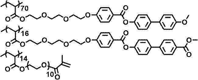
化合物E-1

化合物E-2

界面活性剤F-1
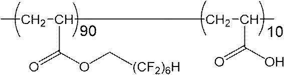
[色味調整層C1の形成]
得られた光吸収異方性層P1上に、下記色味調整層形成用組成物C1をワイヤーバーで連続的に塗布し、塗膜を形成した。
次いで、塗膜が形成された支持体を60℃の温風で60秒間、さらに100℃の温風で120秒間乾燥して色味調整層C1を形成し、光学フィルム1とした。色味調整層の膜厚は0.5μmであった。
―――――――――――――――――――――――――――――――――
(色味調整層形成用組成物C1)
―――――――――――――――――――――――――――――――――
・上記変性ポリビニルアルコールPVA-1 3.80質量部
・IRGACURE 2959 0.20質量部
・下記色素化合物G-1 0.08質量部
・水 70質量部
・メタノール 30質量部
―――――――――――――――――――――――――――――――――
得られた光吸収異方性層P1上に、下記色味調整層形成用組成物C1をワイヤーバーで連続的に塗布し、塗膜を形成した。
次いで、塗膜が形成された支持体を60℃の温風で60秒間、さらに100℃の温風で120秒間乾燥して色味調整層C1を形成し、光学フィルム1とした。色味調整層の膜厚は0.5μmであった。
―――――――――――――――――――――――――――――――――
(色味調整層形成用組成物C1)
―――――――――――――――――――――――――――――――――
・上記変性ポリビニルアルコールPVA-1 3.80質量部
・IRGACURE 2959 0.20質量部
・下記色素化合物G-1 0.08質量部
・水 70質量部
・メタノール 30質量部
―――――――――――――――――――――――――――――――――
色素化合物G-1

[光学積層体A1の作製]
国際公開第2015/166991号記載の片面保護膜付偏光板02と同様の方法で、偏光子の厚さが8μmで、偏光子の片面がむき出しの偏光板1を作製した。
前記偏光板1の偏光子がむき出しの面と、作製した光学フィルム1の光吸収異方性層表面をコロナ処理し、下記のPVA接着剤1を用いて貼合し、光学積層体A1を作製した。
国際公開第2015/166991号記載の片面保護膜付偏光板02と同様の方法で、偏光子の厚さが8μmで、偏光子の片面がむき出しの偏光板1を作製した。
前記偏光板1の偏光子がむき出しの面と、作製した光学フィルム1の光吸収異方性層表面をコロナ処理し、下記のPVA接着剤1を用いて貼合し、光学積層体A1を作製した。
(PVA接着剤1の調製)
アセトアセチル基を含有するポリビニルアルコール系樹脂(平均重合度:1200、ケン化度:98.5モル%、アセトアセチル化度:5モル%)100部に対し、メチロールメラミン20部を、30℃の温度条件下で純水に溶解し、固形分濃度3.7%に調整した水溶液を調製した。
アセトアセチル基を含有するポリビニルアルコール系樹脂(平均重合度:1200、ケン化度:98.5モル%、アセトアセチル化度:5モル%)100部に対し、メチロールメラミン20部を、30℃の温度条件下で純水に溶解し、固形分濃度3.7%に調整した水溶液を調製した。
[画像表示装置I1の作製]
IPSモードの液晶表示装置であるiPad Air(登録商標) Wi-Fiモデル 16GB (APPLE社製)を分解し、液晶セルを取り出した。液晶セルから視認側偏光板を剥離し、視認側偏光板を剥離した面に、上記作製した光学積層体A1を、偏光板1側が液晶セル側になるようにして、下記の粘着剤シート1を用いて貼合した。このとき、偏光板1の吸収軸の方向は、製品に貼合されていた視認側偏光板の吸収軸と同じになるように貼合した。貼合後、組み立て直し、画像表示装置I1を作製した。
IPSモードの液晶表示装置であるiPad Air(登録商標) Wi-Fiモデル 16GB (APPLE社製)を分解し、液晶セルを取り出した。液晶セルから視認側偏光板を剥離し、視認側偏光板を剥離した面に、上記作製した光学積層体A1を、偏光板1側が液晶セル側になるようにして、下記の粘着剤シート1を用いて貼合した。このとき、偏光板1の吸収軸の方向は、製品に貼合されていた視認側偏光板の吸収軸と同じになるように貼合した。貼合後、組み立て直し、画像表示装置I1を作製した。
(粘着剤シート1の作製)
以下の手順に従い、アクリレート系ポリマーを調製した。
冷却管、窒素導入管、温度計および撹拌装置を備えた反応容器において、アクリル酸ブチル95質量部、アクリル酸5質量部を混合し、溶液重合法により重合させて、平均分子量200万、分子量分布(Mw/Mn)3.0のアクリレート系重合体PL1を得た。
以下の手順に従い、アクリレート系ポリマーを調製した。
冷却管、窒素導入管、温度計および撹拌装置を備えた反応容器において、アクリル酸ブチル95質量部、アクリル酸5質量部を混合し、溶液重合法により重合させて、平均分子量200万、分子量分布(Mw/Mn)3.0のアクリレート系重合体PL1を得た。
次に、得られたアクリレート系ポリマーPL1(100質量部)に加えて、コロネートL(トリレンジイソシアネ-トのトリメチロールプロパン付加物の75質量%酢酸エチル溶液、1分子中のイソシアネート基数:3個、日本ポリウレタン工業株式会社製)(1.0質量部)、および、シランカップリング剤KBM-403(信越化学工業社製)(0.2質量部)を混合し、最後に全固形分濃度が10質量%となるように酢酸エチルを添加して、粘着剤形成用組成物を調製した。この組成物を、シリコーン系剥離剤で表面処理したセパレートフィルムにダイコーターを用いて塗布し90℃の環境下で1分間乾燥させ、アクリレート系粘着剤シートを得た。粘着剤シートの膜厚は25μm、貯蔵弾性率は0.1MPaであった。
<実施例2>
実施例1の光学フィルム1において、色味調整層形成用組成物C1を色味調整層形成用組成物C2に変更した以外は、実施例1と同様にして、実施例2の光学フィルム2を作製した。
―――――――――――――――――――――――――――――――――
(色味調整層形成用組成物C2)
―――――――――――――――――――――――――――――――――
・上記変性ポリビニルアルコールPVA-1 3.80質量部
・IRGACURE 2959 0.20質量部
・下記色素化合物G-2 0.01質量部
・水 70質量部
・メタノール 30質量部
―――――――――――――――――――――――――――――――――
実施例1の光学フィルム1において、色味調整層形成用組成物C1を色味調整層形成用組成物C2に変更した以外は、実施例1と同様にして、実施例2の光学フィルム2を作製した。
―――――――――――――――――――――――――――――――――
(色味調整層形成用組成物C2)
―――――――――――――――――――――――――――――――――
・上記変性ポリビニルアルコールPVA-1 3.80質量部
・IRGACURE 2959 0.20質量部
・下記色素化合物G-2 0.01質量部
・水 70質量部
・メタノール 30質量部
―――――――――――――――――――――――――――――――――
色素化合物G-2

<実施例3>
実施例1の光吸収異方性層形成用組成物P1において、二色性物質D-3を二色性物質D-4に変更した光吸収異方性層形成用組成物P2を用いたこと以外は実施例1と同様にして、光学フィルム3を作製した。
実施例1の光吸収異方性層形成用組成物P1において、二色性物質D-3を二色性物質D-4に変更した光吸収異方性層形成用組成物P2を用いたこと以外は実施例1と同様にして、光学フィルム3を作製した。
色素化合物D-4

<実施例4>
実施例1の光吸収異方性層形成用組成物P1に代えて、光吸収異方性層形成用組成物P3を用いたこと以外は実施例1と同様にして、光学フィルム4を作製した。
―――――――――――――――――――――――――――――――――
光吸収異方性層形成用組成物P3の組成
―――――――――――――――――――――――――――――――――
・上記二色性物質D-1 0.63質量部
・上記二色性物質D-2 0.17質量部
・下記二色性物質D-5 1.13質量部
・下記液晶性化合物L-1 5.45質量部
・下記液晶性化合物L-2 2.72質量部
・IRGACURE OXE-02(BASF社製) 0.16質量部
・上記化合物E-1 0.12質量部
・上記化合物E-2 0.12質量部
・上記界面活性剤F-1 0.005質量部
・シクロペンタノン 85.00質量部
・ベンジルアルコール 4.50質量部
―――――――――――――――――――――――――――――――――
実施例1の光吸収異方性層形成用組成物P1に代えて、光吸収異方性層形成用組成物P3を用いたこと以外は実施例1と同様にして、光学フィルム4を作製した。
―――――――――――――――――――――――――――――――――
光吸収異方性層形成用組成物P3の組成
―――――――――――――――――――――――――――――――――
・上記二色性物質D-1 0.63質量部
・上記二色性物質D-2 0.17質量部
・下記二色性物質D-5 1.13質量部
・下記液晶性化合物L-1 5.45質量部
・下記液晶性化合物L-2 2.72質量部
・IRGACURE OXE-02(BASF社製) 0.16質量部
・上記化合物E-1 0.12質量部
・上記化合物E-2 0.12質量部
・上記界面活性剤F-1 0.005質量部
・シクロペンタノン 85.00質量部
・ベンジルアルコール 4.50質量部
―――――――――――――――――――――――――――――――――
二色性物質D-5

液晶性化合物L-1

液晶性化合物L-2

<実施例5>
実施例1の光学フィルム1において、色味調整層形成用組成物C1を色味調整層形成用組成物C3に変更した以外は、実施例1と同様にして、光学フィルム5を作製した。
―――――――――――――――――――――――――――――――――
(色味調整層形成用組成物C3)
―――――――――――――――――――――――――――――――――
・上記変性ポリビニルアルコールPVA-1 3.80質量部
・IRGACURE 2959 0.20質量部
・下記色素化合物G-3 0.16質量部
・水 70質量部
・メタノール 30質量部
―――――――――――――――――――――――――――――――――
実施例1の光学フィルム1において、色味調整層形成用組成物C1を色味調整層形成用組成物C3に変更した以外は、実施例1と同様にして、光学フィルム5を作製した。
―――――――――――――――――――――――――――――――――
(色味調整層形成用組成物C3)
―――――――――――――――――――――――――――――――――
・上記変性ポリビニルアルコールPVA-1 3.80質量部
・IRGACURE 2959 0.20質量部
・下記色素化合物G-3 0.16質量部
・水 70質量部
・メタノール 30質量部
―――――――――――――――――――――――――――――――――
色素化合物G-3

<比較例1>
実施例1の光学フィルム1において、色味調整層を設けなかった以外は実施例1と同様にして、光学フィルム6を作製した。
実施例1の光学フィルム1において、色味調整層を設けなかった以外は実施例1と同様にして、光学フィルム6を作製した。
<比較例2>
比較例1の光学フィルム6において、光吸収異方性層形成用組成物を下記P4としたこと以外は比較例1と同様にして、光学フィルム7を作製した。
―――――――――――――――――――――――――――――――――
光吸収異方性層形成用組成物P4の組成
―――――――――――――――――――――――――――――――――
・上記二色性物質D-1 0.75質量部
・上記二色性物質D-2 0.34質量部
・上記二色性物質D-3 1.13質量部
・上記高分子液晶性化合物P-1 7.88質量部
・IRGACURE OXE-02(BASF社製) 0.16質量部
・上記化合物E-1 0.12質量部
・上記化合物E-2 0.12質量部
・上記界面活性剤F-1 0.005質量部
・シクロペンタノン 85.00質量部
・ベンジルアルコール 4.50質量部
―――――――――――――――――――――――――――――――――
比較例1の光学フィルム6において、光吸収異方性層形成用組成物を下記P4としたこと以外は比較例1と同様にして、光学フィルム7を作製した。
―――――――――――――――――――――――――――――――――
光吸収異方性層形成用組成物P4の組成
―――――――――――――――――――――――――――――――――
・上記二色性物質D-1 0.75質量部
・上記二色性物質D-2 0.34質量部
・上記二色性物質D-3 1.13質量部
・上記高分子液晶性化合物P-1 7.88質量部
・IRGACURE OXE-02(BASF社製) 0.16質量部
・上記化合物E-1 0.12質量部
・上記化合物E-2 0.12質量部
・上記界面活性剤F-1 0.005質量部
・シクロペンタノン 85.00質量部
・ベンジルアルコール 4.50質量部
―――――――――――――――――――――――――――――――――
<比較例3>
実施例3の光学フィルム3において、色味調整層を設けなかったこと以外は実施例3と同様にして、光学フィルム8を作製した。
実施例3の光学フィルム3において、色味調整層を設けなかったこと以外は実施例3と同様にして、光学フィルム8を作製した。
<実施例6>
[光配向層の形成]
実施例1と同様にして、配向膜付きTACフィルム1を作製し、配向膜AL1上に下記光配向層形成用組成液E1を塗布し、60℃で2分間乾燥した。その後、得られた塗布膜に、紫外線露光装置を用いて紫外線(照射量2000mJ/cm2)を膜法線方向を基準として極角15°方向より照射し、厚み0.03μmの光配向層E1を作製した。
[光配向層の形成]
実施例1と同様にして、配向膜付きTACフィルム1を作製し、配向膜AL1上に下記光配向層形成用組成液E1を塗布し、60℃で2分間乾燥した。その後、得られた塗布膜に、紫外線露光装置を用いて紫外線(照射量2000mJ/cm2)を膜法線方向を基準として極角15°方向より照射し、厚み0.03μmの光配向層E1を作製した。
[光配向層形成用組成液E1の調製]
下記の組成にて、光配向層形成用組成液E1を調製し、攪拌しながら1時間溶解し、
溶解後、0.45μmフィルターでろ過し、光配向層形成用組成液E1を得た。
――――――――――――――――――――――――――――――――
光配向層形成用組成液E1
――――――――――――――――――――――――――――――――
・下記光配向材料E-3 0.3質量部
・2-ブトキシエタノール 41.6質量部
・ジプロピレングリコールモノメチルエーテル 41.6質量部
・純水 16.5質量部
――――――――――――――――――――――――――――――――
下記の組成にて、光配向層形成用組成液E1を調製し、攪拌しながら1時間溶解し、
溶解後、0.45μmフィルターでろ過し、光配向層形成用組成液E1を得た。
――――――――――――――――――――――――――――――――
光配向層形成用組成液E1
――――――――――――――――――――――――――――――――
・下記光配向材料E-3 0.3質量部
・2-ブトキシエタノール 41.6質量部
・ジプロピレングリコールモノメチルエーテル 41.6質量部
・純水 16.5質量部
――――――――――――――――――――――――――――――――
光配向材料E-3

[光吸収異方性層P9の形成]
得られた光配向層E1上に、光吸収異方性層形成用組成物P1をワイヤーバーで連続的に塗布し、120℃で60秒間加熱した後、室温(23℃)になるまで冷却した。
次いで、80℃で60秒間加熱し、再び室温になるまで冷却した。
その後、LED灯(中心波長365nm)を用いて照度200mW/cm2の照射条件で2秒間照射することにより、配向膜AL1上に光吸収異方性層P9を作製した。
光吸収異方性層P9の膜厚は3.5μmであった。光吸収異方性層P9の透過率中心軸とフィルム法線の角度は15度であった。
得られた光配向層E1上に、光吸収異方性層形成用組成物P1をワイヤーバーで連続的に塗布し、120℃で60秒間加熱した後、室温(23℃)になるまで冷却した。
次いで、80℃で60秒間加熱し、再び室温になるまで冷却した。
その後、LED灯(中心波長365nm)を用いて照度200mW/cm2の照射条件で2秒間照射することにより、配向膜AL1上に光吸収異方性層P9を作製した。
光吸収異方性層P9の膜厚は3.5μmであった。光吸収異方性層P9の透過率中心軸とフィルム法線の角度は15度であった。
[色味調整層C9の形成]
得られた光吸収異方性層P9上に、色味調整層形成用組成物C1を塗布し、実施例1と同様にして光学フィルム9を得た。
得られた光吸収異方性層P9上に、色味調整層形成用組成物C1を塗布し、実施例1と同様にして光学フィルム9を得た。
<実施例7~10>
実施例1の光学フィルム1において、色味調整層の膜厚d(C)を変更し、上記式(7)中のc(C)×d(C))/(c(P)×d(P)で表される値を表2に示す値に調整したこと以外は実施例1と同様にして、光学フィルム10~13を作製した。
実施例1の光学フィルム1において、色味調整層の膜厚d(C)を変更し、上記式(7)中のc(C)×d(C))/(c(P)×d(P)で表される値を表2に示す値に調整したこと以外は実施例1と同様にして、光学フィルム10~13を作製した。
<実施例11>
実施例1の光学フィルム1において、光吸収異方性層P1を形成した後、再度配向膜形成用組成物1を用いて配向膜AL1と同様に配向膜を形成し、その後色味調整層形成用組成物C1を色味調整層形成用組成物C4に変更した以外は、実施例1と同様にして、実施例11の光学フィルム14を作製した。
―――――――――――――――――――――――――――――――――
(色味調整層形成用組成物C4)
―――――――――――――――――――――――――――――――――
・上記二色性物質D-3 1.13質量部
・上記高分子液晶性化合物P-1 9.22質量部
・IRGACURE OXE-02(BASF社製) 0.16質量部
・界面活性剤F-1 0.005質量部
・シクロペンタノン 85.00質量部
・ベンジルアルコール 4.50質量部
―――――――――――――――――――――――――――――――――
実施例1の光学フィルム1において、光吸収異方性層P1を形成した後、再度配向膜形成用組成物1を用いて配向膜AL1と同様に配向膜を形成し、その後色味調整層形成用組成物C1を色味調整層形成用組成物C4に変更した以外は、実施例1と同様にして、実施例11の光学フィルム14を作製した。
―――――――――――――――――――――――――――――――――
(色味調整層形成用組成物C4)
―――――――――――――――――――――――――――――――――
・上記二色性物質D-3 1.13質量部
・上記高分子液晶性化合物P-1 9.22質量部
・IRGACURE OXE-02(BASF社製) 0.16質量部
・界面活性剤F-1 0.005質量部
・シクロペンタノン 85.00質量部
・ベンジルアルコール 4.50質量部
―――――――――――――――――――――――――――――――――
<評価>
[配向度の評価]
(光吸収異方性層)
得られた光吸収異方性層の波長550nmにおける配向度は以下の方法によって算出した。
AxoScan OPMF-1(オプトサイエンス社製)を用いて、測定の際に、光吸収異方性層の法線方向に対する角度である極角を0~90°まで5°ごとに変更しつつ、各極角における波長550nmでのミュラーマトリックスを実測し、最小透過率(Tmin)を導出した。次に、表面反射の影響を除去した後、Tminが最も高くなる極角におけるTminをTm(0)、Tminの最も高い極角からさらに40°極角を大きくした方向のTminをTm(40)とする。得られたTm(0)およびTm(40)から下記式により吸光度(A)を算出し、A(0)およびA(40)を算出した。
A=-log(Tm)
ここで、Tmは透過率、Aは吸光度を表す。
算出したA(0)およびA(40)より、下記式で定義された波長550nmにおける配向度SPを算出した。
SP=(4.6×A(40)-A(0))/(4.6×A(40)+2×A(0))
上記波長を550nmから420nmまたは650nmに変更することにより、波長420nmおよび650nmおける配向度SPを算出した。
[配向度の評価]
(光吸収異方性層)
得られた光吸収異方性層の波長550nmにおける配向度は以下の方法によって算出した。
AxoScan OPMF-1(オプトサイエンス社製)を用いて、測定の際に、光吸収異方性層の法線方向に対する角度である極角を0~90°まで5°ごとに変更しつつ、各極角における波長550nmでのミュラーマトリックスを実測し、最小透過率(Tmin)を導出した。次に、表面反射の影響を除去した後、Tminが最も高くなる極角におけるTminをTm(0)、Tminの最も高い極角からさらに40°極角を大きくした方向のTminをTm(40)とする。得られたTm(0)およびTm(40)から下記式により吸光度(A)を算出し、A(0)およびA(40)を算出した。
A=-log(Tm)
ここで、Tmは透過率、Aは吸光度を表す。
算出したA(0)およびA(40)より、下記式で定義された波長550nmにおける配向度SPを算出した。
SP=(4.6×A(40)-A(0))/(4.6×A(40)+2×A(0))
上記波長を550nmから420nmまたは650nmに変更することにより、波長420nmおよび650nmおける配向度SPを算出した。
(色味調整層)
得られた光学フィルムから、粘着剤を介して色味調整層のみをセルロースアシレートフィルム(厚み40μmのTAC基材;TG40 富士フイルム社)に転写した。色味調整層の配向度SCはこの転写したフィルムを用い、光吸収異方性層と同様にして求めた。
得られた光学フィルムから、粘着剤を介して色味調整層のみをセルロースアシレートフィルム(厚み40μmのTAC基材;TG40 富士フイルム社)に転写した。色味調整層の配向度SCはこの転写したフィルムを用い、光吸収異方性層と同様にして求めた。
[透過率および色味の評価]
上記作製した画像表示装置I1を、測定機(EZ-Contrast XL88、ELDIM社製)を用いて、白表示画面の透過率中心軸の輝度Y(0)A1、透過率中心軸とフィルム法線のなす面における、透過率中心軸から30°ずらした方向(斜め方向)の輝度Y(30)A1、透過率中心軸の色味a*(0)A1、b*(0)A1、透過率中心軸とフィルム法線のなす面における、透過率中心軸から30°ずらした方向の色味a*(30)A1、b*(30)A1を測定した。
また、画像表示装置I1の作製において、光吸収異方性層がない光学積層体を液晶セルに貼合した以外は、実施例1と同様にして、画像表示装置Bを作製し、上記記載と同様にして、白表示画面の極角0°(正面方向)の輝度Y(0)Bを測定した。光吸収異方性層を含まない画像表示装置Bの輝度と比較することで、正面透過率T(0)を求めた。
具体的には、下記式を用いて算出した。
T(0)=Y(0)A1/Y(0)B
透過率および色味はそれぞれ下記の評価基準に従って評価した。
上記作製した画像表示装置I1を、測定機(EZ-Contrast XL88、ELDIM社製)を用いて、白表示画面の透過率中心軸の輝度Y(0)A1、透過率中心軸とフィルム法線のなす面における、透過率中心軸から30°ずらした方向(斜め方向)の輝度Y(30)A1、透過率中心軸の色味a*(0)A1、b*(0)A1、透過率中心軸とフィルム法線のなす面における、透過率中心軸から30°ずらした方向の色味a*(30)A1、b*(30)A1を測定した。
また、画像表示装置I1の作製において、光吸収異方性層がない光学積層体を液晶セルに貼合した以外は、実施例1と同様にして、画像表示装置Bを作製し、上記記載と同様にして、白表示画面の極角0°(正面方向)の輝度Y(0)Bを測定した。光吸収異方性層を含まない画像表示装置Bの輝度と比較することで、正面透過率T(0)を求めた。
具体的には、下記式を用いて算出した。
T(0)=Y(0)A1/Y(0)B
透過率および色味はそれぞれ下記の評価基準に従って評価した。
(透過率の評価基準)
A:T(0)が75%以上
B:T(0)が65%以上75%未満
C:T(0)が65%未満
A:T(0)が75%以上
B:T(0)が65%以上75%未満
C:T(0)が65%未満
(色味の評価基準)
A:|a*(0)|が3未満
B:|a*(0)|が3以上5未満
C:|a*(0)|が5以上
また、b*(0)、a*(30)、および、b*(30)も同様にして評価した。
A:|a*(0)|が3未満
B:|a*(0)|が3以上5未満
C:|a*(0)|が5以上
また、b*(0)、a*(30)、および、b*(30)も同様にして評価した。
また、光学フィルム1を光学フィルム2~8に代えて作製した画像表示装置をそれぞれI2~I8とし、同様の方法で透過率および色味の評価を行った。
評価結果を表1に示す。
表1中、「極角」は、光学フィルムの法線方向に対する、光学フィルムの透過率中心軸の角度を表す。
表1中、「配向度」列の「A」表記は、上記方法を用い、450nm、550nm、および、650nmで測定した色味調整層の配向度SCが、いずれも0.1未満であったことを表す。すなわち、「配向度」列の「A」表記は、上記要件1~3の全てを満たすことを表す。また、表1中、「色味調整層の配向度」列の「B」の表記は、450nm、550nm、および、650nmで測定した色味調整層の配向度SCのいずれかが0.1以上であったことを表す。
表1中、「SP(450)」、「SP(550)」、および、「SP(650)」は、それぞれ450nm、550nm、および、650nmで測定した光学フィルムの配向度を表す。
表1中、「SP(450)<SP(550)」、および、「SP(450)<SP(650)」列の「A」表記は、それぞれの不等式が成立することを表し、「B」表記はそれぞれの不等式が成立しないことを表す。なお、「SP(450)<SP(550)」、および、「SP(450)<SP(650)」は、それぞれ上記式(1)および式(2)に対応する。
表1中、「配向度」列の「A」表記は、上記方法を用い、450nm、550nm、および、650nmで測定した色味調整層の配向度SCが、いずれも0.1未満であったことを表す。すなわち、「配向度」列の「A」表記は、上記要件1~3の全てを満たすことを表す。また、表1中、「色味調整層の配向度」列の「B」の表記は、450nm、550nm、および、650nmで測定した色味調整層の配向度SCのいずれかが0.1以上であったことを表す。
表1中、「SP(450)」、「SP(550)」、および、「SP(650)」は、それぞれ450nm、550nm、および、650nmで測定した光学フィルムの配向度を表す。
表1中、「SP(450)<SP(550)」、および、「SP(450)<SP(650)」列の「A」表記は、それぞれの不等式が成立することを表し、「B」表記はそれぞれの不等式が成立しないことを表す。なお、「SP(450)<SP(550)」、および、「SP(450)<SP(650)」は、それぞれ上記式(1)および式(2)に対応する。

表1より、実施例および比較例の結果を比較すると、実施例の光学フィルムは広角色味抑制性に優れることが確認された。
表1より、実施例の結果を比較すると、光吸収異方性層が上記式(1)および(2)を満たすと、光学フィルムは透過率により優れることが確認された。
表1より、光吸収異方性層に含まれる二色性色素化合物のうち、少なくとも1種が上記式(3)で表される二色性色素化合物であると、光学フィルムは透過率により優れることが確認された。
表1より、色味調整層が、上記要件1~3を満たす場合、光学フィルムは広角色味抑制性により優れることが確認された。
表1より、色味調整層に含まれる有機色素化合物の吸収ピーク波長が、500~650nmである場合、光学フィルムは広角色味抑制性により優れることが確認された。
表1より、実施例の結果を比較すると、光吸収異方性層が上記式(1)および(2)を満たすと、光学フィルムは透過率により優れることが確認された。
表1より、光吸収異方性層に含まれる二色性色素化合物のうち、少なくとも1種が上記式(3)で表される二色性色素化合物であると、光学フィルムは透過率により優れることが確認された。
表1より、色味調整層が、上記要件1~3を満たす場合、光学フィルムは広角色味抑制性により優れることが確認された。
表1より、色味調整層に含まれる有機色素化合物の吸収ピーク波長が、500~650nmである場合、光学フィルムは広角色味抑制性により優れることが確認された。
表2に、実施例1、7~10、および、比較例1について上記式(7)と色味について評価した結果を示す。
なお、色味調整層の配向度は420nm、550nm、および、650nmのいずれで測定しても0であった。
表2中、「(c(C)×d(C))/(c(P)×d(P))」の表記は上記式(7)に対応する値である。
なお、色味調整層の配向度は420nm、550nm、および、650nmのいずれで測定しても0であった。
表2中、「(c(C)×d(C))/(c(P)×d(P))」の表記は上記式(7)に対応する値である。
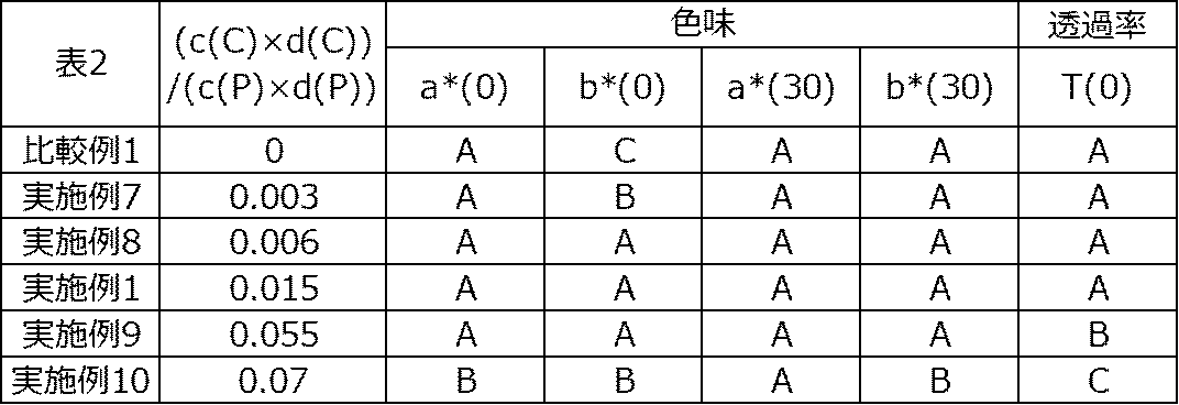
表2より、光学フィルムが上記式(7)を満たす場合、光学フィルムは広角色味抑制性により優れることが確認された。
(曲面加工適正確認)
[曲面加工適正性]
曲面を有するスマートフォン(Galaxy Note9 サムスン製)の表示画面に、実施例1で作製した光学積層体A1を光学フィルム1側が表示画面側になるようにして、市販の粘着剤SK2057(綜研化学製)を用いて貼合した。光学積層体A1は膜厚が100μm以下で柔軟性が高く、表示画面の曲面部分においても気泡が入らず、きれいに貼合できた。
続いて、本発明の光学フィルムと同様の性能を持つ、市場に多く普及しているルーバータイプの光学フィルム(3M(商標) セキュリティ/プライバシーフィルター PF12 H2シリーズ)を上記スマートフォンの表示画面上に、市販の粘着剤SK2057(綜研化学製)を用いて貼合した。上記ルーバータイプの光学フィルムは、膜厚が500μmで柔軟性が低く、表示画面の曲面部分において気泡が入ってしまい、きれいに貼合することができなかった。
[曲面加工適正性]
曲面を有するスマートフォン(Galaxy Note9 サムスン製)の表示画面に、実施例1で作製した光学積層体A1を光学フィルム1側が表示画面側になるようにして、市販の粘着剤SK2057(綜研化学製)を用いて貼合した。光学積層体A1は膜厚が100μm以下で柔軟性が高く、表示画面の曲面部分においても気泡が入らず、きれいに貼合できた。
続いて、本発明の光学フィルムと同様の性能を持つ、市場に多く普及しているルーバータイプの光学フィルム(3M(商標) セキュリティ/プライバシーフィルター PF12 H2シリーズ)を上記スマートフォンの表示画面上に、市販の粘着剤SK2057(綜研化学製)を用いて貼合した。上記ルーバータイプの光学フィルムは、膜厚が500μmで柔軟性が低く、表示画面の曲面部分において気泡が入ってしまい、きれいに貼合することができなかった。
[パターン形成品の評価]
上記領域Aと領域Bのパターンを有する光吸収異方性層を下記のように作製し、評価した。
上記領域Aと領域Bのパターンを有する光吸収異方性層を下記のように作製し、評価した。
(パターン光吸収異方性層の形成)
実施例1の配向膜AL1上に、上記の光吸収異方性層形成用組成物P1をワイヤーバーで連続的に塗布し、塗布層P1を形成した。
次いで、塗布層P1を140℃で30秒間加熱し、塗布層P1を室温(23℃)になるまで冷却した。
次いで、80℃で60秒間加熱し、再び室温になるまで冷却した。
その後、高圧水銀灯が出射する光を、マスクを介して、照度28mW/cm2の照射条件で60秒間照射することにより、配向膜AL1上に、面内に液晶性化合物の硬化領域と未硬化領域とを有する光吸収異方性層を作製した。なお、マスクは、領域Aとして縦10mm×横50mmの長方形の光透過部を有する、遮光部(領域B)と光透過部とを有するマスクパターンとした。
作製した面内に液晶性化合物の硬化領域(領域A)と未硬化領域(領域B)とを有する偏光層を有するフィルムを、エタノール中に3分間浸漬して、重合していない液晶性化合物を洗浄除去し、面内に偏光度の異なる領域Aおよび領域Bを有するパターン光吸収異方性層を有するパターン光学フィルム10を形成した。領域Aは、極角30°透過率が10%以下であり、正面透過率が80%以上であった。領域Bは、極角30°透過率も正面透過率も80%以上であった。
-光学積層体A10の作製-
偏光板1の偏光子がむき出し面と、前記作製したパターン光学フィルム10の光吸収異方性層表面とを、上記粘着剤シート1を用いて貼合し、光学積層体A10を作製した。
実施例1の配向膜AL1上に、上記の光吸収異方性層形成用組成物P1をワイヤーバーで連続的に塗布し、塗布層P1を形成した。
次いで、塗布層P1を140℃で30秒間加熱し、塗布層P1を室温(23℃)になるまで冷却した。
次いで、80℃で60秒間加熱し、再び室温になるまで冷却した。
その後、高圧水銀灯が出射する光を、マスクを介して、照度28mW/cm2の照射条件で60秒間照射することにより、配向膜AL1上に、面内に液晶性化合物の硬化領域と未硬化領域とを有する光吸収異方性層を作製した。なお、マスクは、領域Aとして縦10mm×横50mmの長方形の光透過部を有する、遮光部(領域B)と光透過部とを有するマスクパターンとした。
作製した面内に液晶性化合物の硬化領域(領域A)と未硬化領域(領域B)とを有する偏光層を有するフィルムを、エタノール中に3分間浸漬して、重合していない液晶性化合物を洗浄除去し、面内に偏光度の異なる領域Aおよび領域Bを有するパターン光吸収異方性層を有するパターン光学フィルム10を形成した。領域Aは、極角30°透過率が10%以下であり、正面透過率が80%以上であった。領域Bは、極角30°透過率も正面透過率も80%以上であった。
-光学積層体A10の作製-
偏光板1の偏光子がむき出し面と、前記作製したパターン光学フィルム10の光吸収異方性層表面とを、上記粘着剤シート1を用いて貼合し、光学積層体A10を作製した。
-画像表示装置I10の作製-
上記画像表示装置I1と同様にして、光学積層体A1を光学積層体A10に変更して、画像表示装置I10を作製した。領域Aの部分のみが狭視野角であり、正面からのみはっきりと視認できた。
上記画像表示装置I1と同様にして、光学積層体A1を光学積層体A10に変更して、画像表示装置I10を作製した。領域Aの部分のみが狭視野角であり、正面からのみはっきりと視認できた。
[表面凹凸付与品評価]
上記表面凹凸付与した光学積層体を下記のように作製し、評価した。
上記表面凹凸付与した光学積層体を下記のように作製し、評価した。
(画像表示装置I11の作製)
Ra90nmの表面凹凸を付与するために、特許6093153号公報の実施例3に記載の表面凹凸フィルムを、偏光板1の偏光子がむき出しの面に、上記粘着剤シート1を用いて貼合し、光学積層体A11を作製した。
上記画像表示装置I1と同様にして、光学積層体A1を光学積層体A11に変更して、画像表示装置I11を作製した。
Ra90nmの表面凹凸を付与するために、特許6093153号公報の実施例3に記載の表面凹凸フィルムを、偏光板1の偏光子がむき出しの面に、上記粘着剤シート1を用いて貼合し、光学積層体A11を作製した。
上記画像表示装置I1と同様にして、光学積層体A1を光学積層体A11に変更して、画像表示装置I11を作製した。
(画像表示装置I12の作製)
Ra50nmの表面凹凸を付与するために、特許5909454号公報の実施例101に記載の表面凹凸フィルムを、偏光板1の偏光子がむき出しの面に、上記粘着剤シート1を用いて貼合し、光学積層体A12を作製した。
上記画像表示装置I1と同様にして、光学積層体A1を光学積層体A12に変更して、画像表示装置I12を作製した。
Ra50nmの表面凹凸を付与するために、特許5909454号公報の実施例101に記載の表面凹凸フィルムを、偏光板1の偏光子がむき出しの面に、上記粘着剤シート1を用いて貼合し、光学積層体A12を作製した。
上記画像表示装置I1と同様にして、光学積層体A1を光学積層体A12に変更して、画像表示装置I12を作製した。
(画像表示装置I13の作製)
Ra130nmの表面凹凸を付与するために、特許6093153号公報の実施例7に記載の表面凹凸フィルムを、偏光板1の偏光子がむき出し面に、上記粘着剤シート1を用いて貼合し、光学積層体A13を作製した。
上記画像表示装置I1と同様にして、光学積層体A1を光学積層体A13に変更して、画像表示装置I13を作製した。
Ra130nmの表面凹凸を付与するために、特許6093153号公報の実施例7に記載の表面凹凸フィルムを、偏光板1の偏光子がむき出し面に、上記粘着剤シート1を用いて貼合し、光学積層体A13を作製した。
上記画像表示装置I1と同様にして、光学積層体A1を光学積層体A13に変更して、画像表示装置I13を作製した。
(評価:アンチブロッキング性)
実施例の各光学積層体について、光学積層体の最表面同士を貼り合わせた際の貼り付き性を、下記基準で評価した。貼り合わせた光学積層体は同じ実施例の光学積層体である。例えば、光学積層体A1は、2枚の光学積層体A1を貼り合わせた。このように同じ実施例の光学積層体同士を貼り合わせて評価を行うことにより、他の表面と貼り合わせてアンチブロッキング性を評価する場合と比べて、光学積層体のアンチブロッキング性を、貼り合わせる他の表面の物性の影響を受けることなく、より正確に評価することができる。
アンチブロッキング性は下記評価基準に従って評価した。
実施例の各光学積層体について、光学積層体の最表面同士を貼り合わせた際の貼り付き性を、下記基準で評価した。貼り合わせた光学積層体は同じ実施例の光学積層体である。例えば、光学積層体A1は、2枚の光学積層体A1を貼り合わせた。このように同じ実施例の光学積層体同士を貼り合わせて評価を行うことにより、他の表面と貼り合わせてアンチブロッキング性を評価する場合と比べて、光学積層体のアンチブロッキング性を、貼り合わせる他の表面の物性の影響を受けることなく、より正確に評価することができる。
アンチブロッキング性は下記評価基準に従って評価した。
-アンチブロッキング性の評価基準-
A:貼り付き感が全く無い。
B:貼り付き感が殆ど無い。
C:貼り付き感が強い。
A:貼り付き感が全く無い。
B:貼り付き感が殆ど無い。
C:貼り付き感が強い。
(評価:狭視野角性)
実施例の各画像表示装置について、正面から視認した場合と、横方向に20度傾斜させて視認した場合の狭視野角性を、下記基準で評価した。
実施例の各画像表示装置について、正面から視認した場合と、横方向に20度傾斜させて視認した場合の狭視野角性を、下記基準で評価した。
-狭視野角性の評価基準-
A:正面と斜めの視認性に明確な差がある。
B:正面と斜めの視認性に差が分かる。
C:斜めからも視認されてしまう。
A:正面と斜めの視認性に明確な差がある。
B:正面と斜めの視認性に差が分かる。
C:斜めからも視認されてしまう。
光学積層体A1、A11、A12、および、A13のアンチブロッキング性、ならびに、画像表示装置I1、I11、I12、および、I13の狭視野角性の評価結果を、それぞれ実施例1、11、12、13として表3に示す。

表3から、本発明の光学積層体の表面凹凸の算術表面粗さRaが50nm以上であると、フィルムを重ねた際のアンチブロッキング性により優れることが確認された。一方、表面凹凸の算術表面粗さRaが130nm未満であると、狭視野角性がより優れることが確認された。
Claims (13)
- 透過率中心軸と層表面の法線方向とのなす角θが0~45°である光吸収異方性層と、少なくとも1種の有機色素化合物を含む色味調整層とを有する、光学フィルム。
- 前記光吸収異方性層が、液晶性化合物と、少なくとも1種の二色性色素化合物とを含む、請求項1に記載の光学フィルム。
- 前記光吸収異方性層が下記式(1)および式(2)をともに満たす、請求項1または2に記載の光学フィルム。
SP(420nm)<SP(550nm) 式(1)
SP(420nm)<SP(650nm) 式(2)
ただし、SP(λnm)は波長λnmで測定される、前記光吸収異方性層の配向度を表す。 - 前記光吸収異方性層に含まれる二色性色素化合物のうち、少なくとも1種が下記式(3)で表される、請求項2または3に記載の光学フィルム。

前記式(3)中、L3およびL4は、それぞれ独立に、置換基を表す。
前記式(3)中、Eは、窒素原子、酸素原子および硫黄原子のいずれかの原子を表す。
前記式(3)中、R1は、水素原子、ハロゲン原子、置換基を有していてもよいアルキル基または置換基を有していてもよいアルコキシ基を表す。
前記式(3)中、R2は、水素原子または置換基を有していてもよいアルキル基を表す。
前記式(3)中、R3は、水素原子または置換基を表す。
前記式(3)中、nは、0または1を表す。ただし、Eが窒素原子である場合には、nは1であり、Eが酸素原子または硫黄原子である場合には、nは0である。 - 前記色味調整層が下記要件1~3のいずれか1つを満たす、請求項1~4のいずれか1項に記載の光学フィルム。
要件1:SC(420nm)<0.1
要件2:SC(550nm)<0.1
要件3:SC(650nm)<0.1
ただし、SC(λnm)は波長λnmで測定される、前記色味調整層の配向度を表す。 - 前記色味調整層に含まれる有機色素化合物の吸収ピーク波長が、500~650nmである、請求項1~5のいずれか1項に記載の光学フィルム。
- 前記色味調整層に含まれる有機色素化合物が、ベンゼン環および複素環の少なくとも一方の構造を分子中に有する、請求項1~6のいずれか1項に記載の光学フィルム。
- 前記色味調整層に含まれる有機色素化合物が、アントラキノン構造を有する、請求項1~7のいずれか1項に記載の光学フィルム。
- 下記式(7)を満たす、請求項1~8のいずれか1項に記載の光学フィルム。
0.005≦(c(C)×d(C))/(c(P)×d(P))≦0.06 式(7)
前記式(7)中、c(C)は、前記色味調整層の全質量に対する、前記色味調整層中の前記有機色素化合物の質量比を表す。
前記式(7)中、d(C)は、前記色味調整層の膜厚(μm)を表す。
前記式(7)中、c(P)は、前記光吸収異方性層の全質量に対する、前記光吸収異方性層中の前記二色性色素化合物の質量比を表す。
前記式(7)中、d(P)は、前記光吸収異方性層の膜厚(μm)を表す。 - 前記透過率中心軸に沿った方向の波長550nmの光の透過率が65%以上である、請求項1~9のいずれか1項に記載の光学フィルム。
- 請求項1~10のいずれか1項に記載の光学フィルムと、二色性物質が膜面に対し水平に配向している偏光子層とを有する、光学積層体。
- 請求項1~10のいずれか1項に記載の光学フィルムと、算術平均粗さRaが35~125nmの凹凸層とを有する、光学積層体。
- 請求項1~10のいずれか1項に記載の光学フィルム、または、請求項11もしくは12に記載の光学積層体を有する、画像表示装置。
Priority Applications (4)
| Application Number | Priority Date | Filing Date | Title |
|---|---|---|---|
| CN202180040049.8A CN115943331B (zh) | 2020-06-05 | 2021-06-02 | 光学膜、光学层叠体及图像显示装置 |
| JP2022528864A JP7573609B2 (ja) | 2020-06-05 | 2021-06-02 | 光学フィルム、光学積層体および画像表示装置 |
| US18/060,878 US20230120853A1 (en) | 2020-06-05 | 2022-12-01 | Optical film, optical laminate, and image display device |
| JP2024092807A JP2024103795A (ja) | 2020-06-05 | 2024-06-07 | 光学フィルム、光学積層体および画像表示装置 |
Applications Claiming Priority (6)
| Application Number | Priority Date | Filing Date | Title |
|---|---|---|---|
| JP2020-098535 | 2020-06-05 | ||
| JP2020098535 | 2020-06-05 | ||
| JP2020-110451 | 2020-06-26 | ||
| JP2020110451 | 2020-06-26 | ||
| JP2021-089433 | 2021-05-27 | ||
| JP2021089433 | 2021-05-27 |
Related Child Applications (1)
| Application Number | Title | Priority Date | Filing Date |
|---|---|---|---|
| US18/060,878 Continuation US20230120853A1 (en) | 2020-06-05 | 2022-12-01 | Optical film, optical laminate, and image display device |
Publications (1)
| Publication Number | Publication Date |
|---|---|
| WO2021246441A1 true WO2021246441A1 (ja) | 2021-12-09 |
Family
ID=78831116
Family Applications (1)
| Application Number | Title | Priority Date | Filing Date |
|---|---|---|---|
| PCT/JP2021/020986 Ceased WO2021246441A1 (ja) | 2020-06-05 | 2021-06-02 | 光学フィルム、光学積層体および画像表示装置 |
Country Status (4)
| Country | Link |
|---|---|
| US (1) | US20230120853A1 (ja) |
| JP (2) | JP7573609B2 (ja) |
| CN (1) | CN115943331B (ja) |
| WO (1) | WO2021246441A1 (ja) |
Cited By (3)
| Publication number | Priority date | Publication date | Assignee | Title |
|---|---|---|---|---|
| WO2023053995A1 (ja) * | 2021-09-29 | 2023-04-06 | 富士フイルム株式会社 | 光吸収異方性層、光学フィルム、視野角制御システムおよび画像表示装置 |
| WO2024127911A1 (ja) * | 2022-12-14 | 2024-06-20 | 富士フイルム株式会社 | 光学積層体および画像表示装置 |
| WO2025253981A1 (ja) * | 2024-06-04 | 2025-12-11 | 富士フイルム株式会社 | 光学フィルム、ヘッドマウントディスプレイ |
Families Citing this family (2)
| Publication number | Priority date | Publication date | Assignee | Title |
|---|---|---|---|---|
| JP7573609B2 (ja) * | 2020-06-05 | 2024-10-25 | 富士フイルム株式会社 | 光学フィルム、光学積層体および画像表示装置 |
| CN116615970A (zh) * | 2020-12-21 | 2023-08-18 | 富士胶片株式会社 | 光学膜、视角控制系统及图像显示装置 |
Citations (3)
| Publication number | Priority date | Publication date | Assignee | Title |
|---|---|---|---|---|
| US3005814A (en) * | 1956-12-05 | 1961-10-24 | Sandoz Ag | Metal-containing polyazo dyestuffs |
| JP2016027387A (ja) * | 2014-06-25 | 2016-02-18 | 住友化学株式会社 | 光吸収異方性膜、3次元光吸収異方性膜及びその製造方法 |
| JP2018045175A (ja) * | 2016-09-16 | 2018-03-22 | 富士フイルム株式会社 | 積層体および物品 |
Family Cites Families (7)
| Publication number | Priority date | Publication date | Assignee | Title |
|---|---|---|---|---|
| JP5025390B2 (ja) * | 2006-09-06 | 2012-09-12 | 富士フイルム株式会社 | 液晶表示装置 |
| JP5418048B2 (ja) * | 2009-05-26 | 2014-02-19 | コニカミノルタ株式会社 | 偏光制御素子、積層偏光制御素子、楕円偏光板、発光素子および偏光特性制御方法 |
| JP2012068273A (ja) * | 2010-09-21 | 2012-04-05 | Nitto Denko Corp | 光拡散素子、光拡散素子付偏光板、およびこれらを用いた液晶表示装置、ならびに光拡散素子の製造方法 |
| JP5136711B2 (ja) * | 2012-04-27 | 2013-02-06 | 住友化学株式会社 | 透過型画像表示装置 |
| JP2015102811A (ja) * | 2013-11-27 | 2015-06-04 | 三星電子株式会社Samsung Electronics Co.,Ltd. | 光学フィルム、発光装置、及び表示装置 |
| JP7311958B2 (ja) * | 2018-11-09 | 2023-07-20 | 住友化学株式会社 | 垂直配向液晶硬化膜およびそれを含む積層体 |
| JP7573609B2 (ja) * | 2020-06-05 | 2024-10-25 | 富士フイルム株式会社 | 光学フィルム、光学積層体および画像表示装置 |
-
2021
- 2021-06-02 JP JP2022528864A patent/JP7573609B2/ja active Active
- 2021-06-02 CN CN202180040049.8A patent/CN115943331B/zh active Active
- 2021-06-02 WO PCT/JP2021/020986 patent/WO2021246441A1/ja not_active Ceased
-
2022
- 2022-12-01 US US18/060,878 patent/US20230120853A1/en active Pending
-
2024
- 2024-06-07 JP JP2024092807A patent/JP2024103795A/ja active Pending
Patent Citations (3)
| Publication number | Priority date | Publication date | Assignee | Title |
|---|---|---|---|---|
| US3005814A (en) * | 1956-12-05 | 1961-10-24 | Sandoz Ag | Metal-containing polyazo dyestuffs |
| JP2016027387A (ja) * | 2014-06-25 | 2016-02-18 | 住友化学株式会社 | 光吸収異方性膜、3次元光吸収異方性膜及びその製造方法 |
| JP2018045175A (ja) * | 2016-09-16 | 2018-03-22 | 富士フイルム株式会社 | 積層体および物品 |
Cited By (3)
| Publication number | Priority date | Publication date | Assignee | Title |
|---|---|---|---|---|
| WO2023053995A1 (ja) * | 2021-09-29 | 2023-04-06 | 富士フイルム株式会社 | 光吸収異方性層、光学フィルム、視野角制御システムおよび画像表示装置 |
| WO2024127911A1 (ja) * | 2022-12-14 | 2024-06-20 | 富士フイルム株式会社 | 光学積層体および画像表示装置 |
| WO2025253981A1 (ja) * | 2024-06-04 | 2025-12-11 | 富士フイルム株式会社 | 光学フィルム、ヘッドマウントディスプレイ |
Also Published As
| Publication number | Publication date |
|---|---|
| CN115943331A (zh) | 2023-04-07 |
| JPWO2021246441A1 (ja) | 2021-12-09 |
| JP2024103795A (ja) | 2024-08-01 |
| US20230120853A1 (en) | 2023-04-20 |
| JP7573609B2 (ja) | 2024-10-25 |
| CN115943331B (zh) | 2025-12-02 |
Similar Documents
| Publication | Publication Date | Title |
|---|---|---|
| JP7109476B2 (ja) | 光学積層体の製造方法、光学積層体および画像表示装置 | |
| TWI855593B (zh) | 光學膜及其製造方法 | |
| JP7573609B2 (ja) | 光学フィルム、光学積層体および画像表示装置 | |
| JP7491660B2 (ja) | 光学補償機能付き位相差板 | |
| JP7553474B2 (ja) | 光吸収異方性層、積層体、光学フィルム、画像表示装置、バックライトモジュール | |
| CN106371164B (zh) | 层叠体、包含层叠体的圆偏振板及具备层叠体的显示装置 | |
| JPWO2020045216A1 (ja) | 積層体および画像表示装置 | |
| WO2019131976A1 (ja) | 光吸収異方性膜、光学積層体および画像表示装置 | |
| JP7428785B2 (ja) | 液晶表示装置 | |
| WO2022270466A1 (ja) | 光学フィルム、光吸収異方性層の製造方法および画像表示装置 | |
| WO2022181414A1 (ja) | 積層体、映り込み防止システム、および、画像表示装置 | |
| JP7699153B2 (ja) | 光吸収異方性フィルム、視角制御システムおよび画像表示装置 | |
| WO2022138504A1 (ja) | 光学フィルム、視角制御システム及び画像表示装置 | |
| TWI808224B (zh) | 光學膜 | |
| JP7529378B2 (ja) | フレキシブルディスプレイ用光学補償機能付き位相差板 | |
| WO2022234789A1 (ja) | 偏光板及び有機el表示装置 | |
| TWI882978B (zh) | 有機el顯示器用積層體 | |
| WO2021230019A1 (ja) | 視角制御システムおよび画像表示装置 | |
| CN116057430B (en) | Optical laminate and elliptical polarizing plate comprising same | |
| WO2023085255A1 (ja) | 有機el表示装置 | |
| WO2025028263A1 (ja) | 光学積層体 | |
| TW202603410A (zh) | 光學積層體及光學積層體的製造方法 |
Legal Events
| Date | Code | Title | Description |
|---|---|---|---|
| 121 | Ep: the epo has been informed by wipo that ep was designated in this application |
Ref document number: 21818070 Country of ref document: EP Kind code of ref document: A1 |
|
| ENP | Entry into the national phase |
Ref document number: 2022528864 Country of ref document: JP Kind code of ref document: A |
|
| NENP | Non-entry into the national phase |
Ref country code: DE |
|
| 122 | Ep: pct application non-entry in european phase |
Ref document number: 21818070 Country of ref document: EP Kind code of ref document: A1 |