WO2021245895A1 - 半導体装置および半導体装置の製造方法 - Google Patents
半導体装置および半導体装置の製造方法 Download PDFInfo
- Publication number
- WO2021245895A1 WO2021245895A1 PCT/JP2020/022215 JP2020022215W WO2021245895A1 WO 2021245895 A1 WO2021245895 A1 WO 2021245895A1 JP 2020022215 W JP2020022215 W JP 2020022215W WO 2021245895 A1 WO2021245895 A1 WO 2021245895A1
- Authority
- WO
- WIPO (PCT)
- Prior art keywords
- layer
- semiconductor
- semiconductor device
- gate electrode
- bandgap
- Prior art date
- Legal status (The legal status is an assumption and is not a legal conclusion. Google has not performed a legal analysis and makes no representation as to the accuracy of the status listed.)
- Ceased
Links
Images





Classifications
-
- H—ELECTRICITY
- H10—SEMICONDUCTOR DEVICES; ELECTRIC SOLID-STATE DEVICES NOT OTHERWISE PROVIDED FOR
- H10D—INORGANIC ELECTRIC SEMICONDUCTOR DEVICES
- H10D30/00—Field-effect transistors [FET]
- H10D30/01—Manufacture or treatment
- H10D30/051—Manufacture or treatment of FETs having PN junction gates
-
- H—ELECTRICITY
- H10—SEMICONDUCTOR DEVICES; ELECTRIC SOLID-STATE DEVICES NOT OTHERWISE PROVIDED FOR
- H10D—INORGANIC ELECTRIC SEMICONDUCTOR DEVICES
- H10D30/00—Field-effect transistors [FET]
- H10D30/01—Manufacture or treatment
- H10D30/061—Manufacture or treatment of FETs having Schottky gates
-
- H—ELECTRICITY
- H10—SEMICONDUCTOR DEVICES; ELECTRIC SOLID-STATE DEVICES NOT OTHERWISE PROVIDED FOR
- H10D—INORGANIC ELECTRIC SEMICONDUCTOR DEVICES
- H10D30/00—Field-effect transistors [FET]
- H10D30/40—FETs having zero-dimensional [0D], one-dimensional [1D] or two-dimensional [2D] charge carrier gas channels
- H10D30/47—FETs having zero-dimensional [0D], one-dimensional [1D] or two-dimensional [2D] charge carrier gas channels having two-dimensional [2D] charge carrier gas channels, e.g. nanoribbon FETs or high electron mobility transistors [HEMT]
-
- H—ELECTRICITY
- H10—SEMICONDUCTOR DEVICES; ELECTRIC SOLID-STATE DEVICES NOT OTHERWISE PROVIDED FOR
- H10D—INORGANIC ELECTRIC SEMICONDUCTOR DEVICES
- H10D30/00—Field-effect transistors [FET]
- H10D30/60—Insulated-gate field-effect transistors [IGFET]
-
- H—ELECTRICITY
- H10—SEMICONDUCTOR DEVICES; ELECTRIC SOLID-STATE DEVICES NOT OTHERWISE PROVIDED FOR
- H10D—INORGANIC ELECTRIC SEMICONDUCTOR DEVICES
- H10D30/00—Field-effect transistors [FET]
- H10D30/80—FETs having rectifying junction gate electrodes
- H10D30/83—FETs having PN junction gate electrodes
-
- H—ELECTRICITY
- H10—SEMICONDUCTOR DEVICES; ELECTRIC SOLID-STATE DEVICES NOT OTHERWISE PROVIDED FOR
- H10D—INORGANIC ELECTRIC SEMICONDUCTOR DEVICES
- H10D30/00—Field-effect transistors [FET]
- H10D30/80—FETs having rectifying junction gate electrodes
- H10D30/87—FETs having Schottky gate electrodes, e.g. metal-semiconductor FETs [MESFET]
-
- H—ELECTRICITY
- H10—SEMICONDUCTOR DEVICES; ELECTRIC SOLID-STATE DEVICES NOT OTHERWISE PROVIDED FOR
- H10D—INORGANIC ELECTRIC SEMICONDUCTOR DEVICES
- H10D62/00—Semiconductor bodies, or regions thereof, of devices having potential barriers
- H10D62/80—Semiconductor bodies, or regions thereof, of devices having potential barriers characterised by the materials
- H10D62/81—Semiconductor bodies, or regions thereof, of devices having potential barriers characterised by the materials of structures exhibiting quantum-confinement effects, e.g. single quantum wells; of structures having periodic or quasi-periodic potential variation
-
- H—ELECTRICITY
- H10—SEMICONDUCTOR DEVICES; ELECTRIC SOLID-STATE DEVICES NOT OTHERWISE PROVIDED FOR
- H10D—INORGANIC ELECTRIC SEMICONDUCTOR DEVICES
- H10D62/00—Semiconductor bodies, or regions thereof, of devices having potential barriers
- H10D62/80—Semiconductor bodies, or regions thereof, of devices having potential barriers characterised by the materials
- H10D62/83—Semiconductor bodies, or regions thereof, of devices having potential barriers characterised by the materials being Group IV materials, e.g. B-doped Si or undoped Ge
Definitions
- This disclosure relates to a semiconductor device and a method for manufacturing the semiconductor device.
- a semiconductor device using Si (silicon) as a base material is known.
- Examples of the structure of the semiconductor device include GTO (Gate Turn-Off thyristor) and IGBT (Insulated Gate Bipolar Transistor). These have a so-called vertical structure.
- GTO Gate Turn-Off thyristor
- IGBT Insulated Gate Bipolar Transistor
- Patent Document 1 proposes a field-effect transistor based on a compound semiconductor having a better physical characteristic constant than Si.
- the material of the compound semiconductor is, for example, SiC (silicon carbide), GaN (gallium nitride), and AlN (aluminum nitride).
- the nitride semiconductor exemplified by GaN and AlN has a high saturated electron velocity, a semiconductor device using the nitride semiconductor as a base material is expected to be driven well at high frequencies.
- Patent Document 2 proposes a semiconductor device having a structure utilizing such modulation.
- the hetero interface in which the two-dimensional electron gas is induced can be formed by adopting a nitride semiconductor.
- Two-dimensional electron gas contributes to lowering the resistance of semiconductor devices.
- Patent Document 3 proposes a semiconductor device having a structure utilizing such a contribution.
- N nitrogen
- nitride semiconductor when p-type impurities are introduced by using the gas phase epitaxial growth method, hydrogen is incorporated in the gas phase reaction.
- the incorporated hydrogen terminates the acceptor impurities and electrically inactivates the acceptor impurities (which can also be described as “electrically” inactivating ").
- the difficulty in electrically activating p-type impurities in nitride semiconductors tends to reduce the effective acceptor impurity concentration in p-type semiconductors. Such a decrease is not desirable from the viewpoint of controllability of the threshold voltage and suppression of punch-through current in the semiconductor device using the pn junction.
- the "polarization barrier” refers to a barrier induced by a polarization charge.
- the polarization barrier can be caused by spontaneous polarization due to the high electronegativity of N, or by piezo polarization due to the difference in lattice constant at the hetero interface, spontaneous polarization and It can also be caused by both piezo polarization.
- the polarization barrier in a nitride semiconductor is formed by bandgap modulation due to the addition of Al.
- the present disclosure has been made to solve the above problems, and an object of the present disclosure is to provide a semiconductor device having high punch-through resistance and a method for manufacturing the semiconductor device.
- the semiconductor device is a semiconductor having an n-type conductivity, which is located on a first layer having a first surface and a second surface facing each other and the first surface, and has an n-type conductivity.
- the semiconductor is a second layer having a first band gap, a second layer located on the second layer, having a second band gap larger than the first band gap, and having n-type conductivity. It has a third layer, which is a true semiconductor, and a third band gap, which is located on the third layer, has a third surface on the opposite side of the third layer, and is smaller than the second band gap.
- the fourth layer which is a semiconductor having n-type conductivity, the drain electrode electrically connected to the first layer on the second surface, and the fourth layer electrically connected to the fourth layer on the third surface.
- the source electrode is located along the first direction in which the second layer, the third layer, and the fourth layer are laminated, and is insulated from the second layer, the third layer, and the fourth layer. At least the third layer is sandwiched between the gate electrode facing the third layer in a second direction different from the first direction and the gate electrode in the second direction, and between the third layer.
- the conduction band is a semiconductor forming a discontinuous interface, or includes a fifth layer having no charge contributing to conduction.
- the method for manufacturing a semiconductor device is a semiconductor having an conductivity of n-type on the first surface of a first layer having a first surface and a second surface facing each other. It is a semiconductor and forms a second layer having a first bandgap, has a second bandgap larger than the first bandgap on the second layer, and is n-type or intrinsically conductive.
- the third layer which is a semiconductor of the above, is formed, and the third layer has a third surface on the opposite side of the third layer, and has a third band gap smaller than the second band gap, and is conductive.
- a fourth layer which is a semiconductor having an n-type property, is formed, and the first region of the third surface penetrates the fourth layer and the third layer to reach the second layer, and then reaches the first layer. Instead, a groove (first groove) that exposes the second layer is formed, and a gate electrode that fills the groove (first groove) and the insulating film are formed via an insulating film.
- the first aspect of the manufacturing method is to inject ions into a second region of the third surface away from the first region to electrically inactivate at least a part of the third layer.
- a source electrode that contacts the third surface at a position sandwiched between the first region and the second region and does not contact the gate electrode is formed, and a drain electrode is formed on the second surface.
- the second layer of the third surface which is separated from the first region, penetrates the fourth layer and the third layer to reach the second layer, and the second layer is formed.
- a second groove to be exposed is formed, and the second groove is filled with a semiconductor having a conduction band discontinuous interface with the third layer or a layer having no charge contributing to conduction.
- a source electrode that contacts the third surface at a position sandwiched between the first region and the second region and does not contact the gate electrode is formed, and a drain electrode is formed on the second surface. ..
- the semiconductor device according to the present disclosure high punch-through resistance can be obtained. According to the method for manufacturing a semiconductor device according to the present disclosure, the semiconductor device according to the present disclosure can be obtained.
- FIG. It is sectional drawing which schematically illustrates the structure of the semiconductor device which concerns on Embodiment 1.
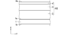
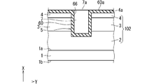
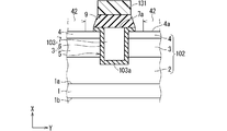
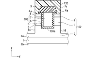
- FIG. It is sectional drawing which illustrates the manufacturing method of the semiconductor device which concerns on Embodiment 1.
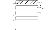
- FIG. It is sectional drawing which illustrates the manufacturing method of the semiconductor device which concerns on Embodiment 1.
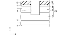
- FIG. It is sectional drawing which illustrates the manufacturing method of the semiconductor device which concerns on Embodiment 1.
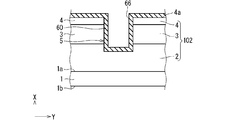
- FIG. It is sectional drawing which illustrates the manufacturing method of the semiconductor device which concerns on Embodiment 1.
- FIG. It is sectional drawing which illustrates the manufacturing method of the semiconductor device which concerns on Embodiment 1.
- FIG. It is sectional drawing which illustrates the manufacturing method of the semiconductor device which concerns on Embodiment 1.
- FIG. It is sectional drawing which illustrates the manufacturing method of the semiconductor device which concerns on Embodiment 1.
- FIG. It is sectional drawing which illustrates the manufacturing method of the semiconductor device which concerns on Embodiment 1.
- FIG. It is sectional drawing which illustrates the manufacturing method of the semiconductor device which concerns on Embodiment 1.
- FIG. It is sectional drawing which illustrates the manufacturing method of the semiconductor device which concerns on Embodiment 1.
- FIG. It is sectional drawing which illustrates the modification of the manufacturing method of the semiconductor device which concerns on Embodiment 1.
- FIG. It is sectional drawing which schematically illustrates the structure of the semiconductor device which concerns on Embodiment 2.
- FIG. It is sectional drawing which schematically illustrates the structure of the semiconductor device which concerns on Embodiment 3.
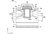
- FIG. It is sectional drawing which schematically illustrates the structure of the semiconductor device which concerns on Embodiment 4.
- the semiconductor device and the method for manufacturing the semiconductor device according to the present disclosure are not limited to these embodiments, and may be appropriately modified without departing from the gist thereof.
- the scale and aspect ratio of each member or each member may differ from the actual scale and aspect ratio, and the same applies between the drawings.
- FIG. 1 is a cross-sectional view schematically illustrating the structure of the semiconductor device 101 according to the first embodiment.
- the semiconductor device 101 includes a first layer 1, a second layer 2, a third layer 3, a fourth layer 4, a fifth layer 8, and an insulated gate electrode 103.
- the first layer 1, the second layer 2, the third layer 3, and the fourth layer 4 are laminated in this order from the bottom to the top in the example in FIG.
- the direction from the first layer 1 to the fourth layer 4 is expressed as the stacking direction X.
- the stacking direction X is shown as a direction from the bottom to the top.
- the direction orthogonal to the stacking direction X is expressed as the direction Y.
- the direction Y is shown as a direction from left to right.
- the expression “vertical direction” is adopted as a general term for the stacking direction X and the direction opposite to the stacking direction X. Such a concept of “vertical” is consistent with “vertical” in so-called vertical structures.
- the first layer 1 is an n-type conductive GaN layer.
- n-type conductive means that the conductivity is n-type.
- the surface 1a of the first layer 1 is in contact with the second layer 2.
- the surface 1a is, for example, a c-plane ((0001) plane) showing Ga polarity.
- the first layer 1 functions as a substrate of the second layer 2.
- the second layer 2 is an n-type conductive GaN layer.
- the second layer 2 functions as a drift layer of the semiconductor device 101.
- the third layer 3 is an n-type conductive Al b Ga (1-b) N layer.
- the third layer 3 functions as a channel layer of the semiconductor device 101.
- b 0.18 is selected.
- the fourth layer 4 is an n-type conductive GaN layer.
- the fourth layer 4 functions as an electron supply layer of the semiconductor device 101.
- the second layer 2, the third layer 3, and the fourth layer 4 are collectively regarded as a laminated semiconductor 102.
- the first layer 1, the second layer 2, the third layer 3, the fourth layer 4, and the laminated semiconductor 102 are all nitride semiconductors. It can be said that the first layer 1 is a substrate of the laminated semiconductor 102.
- the bandgap of the third layer 3 is larger than either the bandgap of the second layer 2 or the bandgap of the fourth layer 4.
- the bandgap of the fourth layer 4 is smaller than the bandgap of the third layer 3.
- a hetero interface is formed between the third layer 3 and the second layer 2 and between the third layer 3 and the fourth layer 4, and a polarization barrier is generated.
- the insulated gate electrode 103 penetrates the 4th layer 4 and the 3rd layer 3 from the surface 4a of the 4th layer 4 opposite to the 2nd layer 2 in the vertical direction, and extends to the 2nd layer 2.
- the surface 103a of the insulated gate electrode 103 closer to the first layer 1 is separated from the surface 1a.
- the second layer 2 exists between the surface 1a and the surface 103a.
- the insulated gate electrode 103 exists in the groove 5 and the surface 4a.
- the groove 5 is formed in the laminated semiconductor 102 and opens in the stacking direction X. It is considered that a part of the insulated gate electrode 103 is embedded in the groove 5.
- the insulated gate electrode 103 has a gate insulating film 6 and a gate electrode 7.
- the gate electrode 7 faces at least the third layer 3 in the lateral direction. In the example of FIG. 1, the gate electrode 7 faces the third layer 3 as well as the fourth layer 4 and a part of the second layer 2 in the lateral direction.
- the gate insulating film 6 exists between the gate electrode 7 and the laminated semiconductor 102.
- the surface 103a is a part of the region where the gate insulating film 6 comes into contact with the laminated semiconductor 102.
- the gate insulating film 6 covers the gate electrode 7 in both the vertical direction and the horizontal direction. In the example of FIG. 1, the gate electrode 7 does not cover the surface 4a in the stacking direction X. The gate insulating film 6 comes into contact with the surface 4a around the gate electrode 7 in the lateral direction.
- the material of the gate insulating film 6 is, for example, silicon oxide (SiO 2 ).
- the material of the gate electrode 7 is, for example, polycrystalline silicon (poly—Si).
- the fifth layer 8 sandwiches at least the third layer 3 between the fifth layer 8 and the gate electrode 7 in the lateral direction.
- the fifth layer 8 sandwiches the third layer 3 and the gate insulating film 6 between the fifth layer 8 and the gate electrode 7 in the lateral direction.
- the fifth layer 8 faces the insulating gate electrode 103 with the third layer 3 interposed therebetween in the lateral direction.
- the fifth layer 8 penetrates the fourth layer 4 and the third layer 3 from the surface 4a in the vertical direction, and extends to the second layer 2.
- the surface 8a of the fifth layer 8 closer to the first layer 1 is separated from the surface 1a.
- the second layer 2 exists between the surface 1a and the surface 8a.
- the fifth layer 8 sandwiches at least the second layer 2 between the fifth layer 8 and the first layer 1 in the vertical direction.
- the fifth layer 8 faces the first layer 1 in the vertical direction with at least the second layer 2 interposed therebetween.
- the fifth layer 8 is considered to narrow the third layer 3 in the lateral direction. From this point of view, the fifth layer 8 can also be referred to as a stenosis layer.
- the fifth layer 8 is a layer having no electric charge that contributes to conduction.
- the fifth layer 8 is, for example, an insulating layer, and may be air.
- the fifth layer 8 is, for example, an electrically activated semiconductor having no impurities. The case where the material of the fifth layer 8 has a charge contributing to conduction will be described later.
- the semiconductor device 101 further includes an interlayer insulating film 9, a source electrode 10, and a drain electrode 11.
- the surface 7a on the X-side in the stacking direction of the gate electrode 7 is covered with the interlayer insulating film 9.
- FIG. 1 the case where the insulating gate electrode 103 is covered with the interlayer insulating film 9 on the X side in the stacking direction is exemplified.
- the gate insulating film 6 covering the fourth layer 4 is covered with the interlayer insulating film 9.
- the interlayer insulating film 9 has a function of insulating between the gate electrode 7 and the source electrode 10.
- the interlayer insulating film 9 faces the surface 4a in the vertical direction via the gate insulating film 6.
- the portion of the surface 4a that is not covered by the gate insulating film 6 is in contact with the source electrode 10, and the fourth layer 4 and the source electrode 10 are electrically connected.
- the case where the fifth layer 8 and the interlayer insulating film 9 are covered with the source electrode 10 on the X side in the stacking direction is exemplified.
- the drain electrode 11 covers the surface 1b of the first layer 1, and the first layer 1 and the drain electrode 11 are electrically connected to each other.
- the surface 1a and the surface 1b face each other with the first layer 1 considered excluding the surfaces 1a and 1b interposed therebetween.
- the stacking direction X is the direction from the surface 1b to the surface 1a.
- the surface 1b is a c-bar surface ((0001 bar) surface) showing N polarity.
- “c bar” means a notation in which an overline is added to the symbol "c" in the normal notation
- “1 bar” means the symbol "1" in the normal notation. Means the notation with an overline added to.
- the source electrode 10 and the drain electrode 11 both have a laminated structure of Ti (titanium) / Al / Ni (nickel) / Au (gold), for example.
- Ti titanium
- Al aluminum
- Ni nickel
- Au gold
- the semiconductor device 101 has a polarization barrier between the fourth layer 4 which is an electron supply layer and the third layer 3 which is a channel layer, and is between the second layer 2 which is a drift layer and the third layer 3 which is a channel layer. Has a polarization barrier.
- p-type conductive nitride semiconductor a nitride semiconductor having p-type conductivity
- p-type conductive nitride semiconductor a nitride semiconductor having p-type conductivity
- avoiding this need enhances the controllability of the threshold voltage (hereinafter referred to as “threshold controllability") in the semiconductor device using the nitride semiconductor as a base material, as compared with the semiconductor device using the pn junction.
- threshold controllability the threshold voltage in the semiconductor device using the nitride semiconductor as a base material
- the semiconductor device 101 functions as a vertical trench MOSFET (Metal-Oxide-Semiconductor Field-Effect Transistor).
- MOSFET Metal-Oxide-Semiconductor Field-Effect Transistor
- the effect of fixing the potential with the p-type conductive nitride semiconductor may not be obtained in the semiconductor device 101. Regardless of the presence or absence of such an effect, in the semiconductor device 101, the punch-through current when a high voltage is applied is reduced by the fifth layer 8.
- the third layer 3 functions as a channel layer, and punch-through is more likely to occur in the channel layer far from the gate electrode 7 than in the channel layer near the gate electrode 7.
- the semiconductor device 101 has a structure in which a portion of the third layer 3 that functions as a channel layer, in which punch-through is likely to occur, is replaced by the fifth layer 8 as compared with the semiconductor device in which the fifth layer 8 does not exist. ..
- the substitution reduces the region where punch-through is likely to occur in the third layer 3, and contributes to the reduction of the punch-through current.
- the semiconductor device 101 has high punch-through resistance as compared with the case where the fifth layer 8 is not present.
- the characteristics of the semiconductor device 101 are unlikely to depend on the impurity activation rate in the p-type conductive nitride semiconductor. The low possibility contributes to the excellent threshold controllability of the semiconductor device 101.
- the thickness, composition, and doping concentration of the second layer 2, the third layer 3, and the fourth layer 4 are designed according to the specifications required for the semiconductor device 101.
- the thickness of the second layer 2 (length in the stacking direction X: the same applies hereinafter) is 10 ⁇ m
- the thickness of the third layer 3 is 1 ⁇ m
- the thickness of the fourth layer 4 is 0.1 ⁇ m.
- These film thicknesses are just an example. Even if the film thickness is other than the above values, it can be arbitrarily selected as long as it does not deviate from the purpose of the present disclosure. These film thicknesses can be appropriately selected according to the requirements based on one or both of the withstand voltage and the on-resistance of the semiconductor device 101.
- the Al a Ga (1-a) N layer may be adopted in the second layer 2, or the Al c Ga (1-c) N layer may be adopted in the fourth layer 4.
- both the second layer 2 and the fourth layer 4 have a smaller Al composition than the third layer 3. According to the illustrated composition ratio, the setting of b> a and b> c is adopted.
- Two types of AlGaN layers bonded with different Al compositions are subjected to an epitaxial growth method (for example, a metalorganic vapor phase epoxy: hereinafter referred to as "MOVPE"). Realized using.
- MOVPE metalorganic vapor phase epoxy
- cracks may occur at the interface where the two types of AlGaN layers are joined due to the mismatch of the lattice constants.
- the Al composition of the third layer 3 is smaller as it is closer to the second layer 2 (as it goes to the side opposite to the stacking direction X) when viewed from the center of the third layer 3.
- the Al composition of the third layer 3 may be larger as it is closer to the center of the third layer 3.
- the Al composition of the third layer 3 does not have to be uniform along the stacking direction X.
- the energy at which the conduction band becomes discontinuous in the polarization barrier is designed to be, for example, 10 times or more the thermal energy (0.026 eV) corresponding to room temperature.
- the discontinuity of the conduction band at the interface where the third layer 3 and the fourth layer 4 are joined is 0.35 eV or more.
- bc ⁇ 0.1 in the above composition ratio is 0.35 eV or more.
- ba ⁇ 0.1 A similar relationship is desired between the third layer 3 and the second layer 2, and ba ⁇ 0.1.
- the second layer 2 is a GaN layer
- composition b of Al in the third layer 3 is less than 1. From the viewpoint of avoiding the occurrence of cracks due to lattice mismatch during epitaxial growth, b ⁇ 0.8 is desirable, and b ⁇ 0.5 is more desirable.
- the Al compositions a, b, and c are 0 ⁇ a ⁇ b-0.1, 0 ⁇ c ⁇ b-0.1, and b ⁇ 1 (preferably b ⁇ 0.8, further. Desirably, b ⁇ 0.5) is satisfied.
- the laminated semiconductor 102 may include an n-type conductive semiconductor and an intrinsic semiconductor (so-called i-type), but it is not necessary to include a p-type conductive semiconductor.
- the AlGaN layer When the AlGaN layer is used as the third layer 3, it may be manufactured intentionally as an intrinsic semiconductor. This is because a so-called UID (unintentionally doped) semiconductor can be obtained.
- Si and oxygen (O) become impurities and are incorporated into the AlGaN layer semiconductor to obtain an AlGaN layer having weak n-type conductivity.
- the above-mentioned Si and O are desorbed from the inner wall of the growth furnace used for epitaxial growth.
- N pores in the step of forming the AlGaN layer an AlGaN layer having weak n-type conductivity can also be obtained.
- the surface 1a may be a c-bar surface showing N polarity.
- the surface 1b is the c surface indicating the Ga polarity.
- the film thickness of the gate insulating film 6 is designed to be, for example, 30 to 100 nm.
- the film thickness of the gate insulating film 6 is 50 nm.
- the material of the gate insulating film 6 As the material of the gate insulating film 6, a material having a bandgap larger than the bandgap of the nitride semiconductor selected for the third layer 3 functioning as the channel layer is selected.
- the electron affinity of the gate insulating film 6 is small, the amount of discontinuity on the conduction band side is large, and an electron barrier between the gate insulating film 6 and the third layer 3 can be easily obtained.
- examples of the material of the gate insulating film 6 include SiO 2 , aluminum oxide (Al 2 O 3 ), silicon nitride (Si 3 N 4 ), aluminum nitride (Al N), hafnium oxide (HfO 2 ), and the like. Examples thereof include lanthanum oxide (La 2 O 3 ) and gadolinium oxide (Gd 2 O 3).
- the materials exemplified here are binary systems, but a mixed crystal system or a multilayer composite film in which two or more of these are combined may be adopted as the gate insulating film 6.
- the material of the gate insulating film 6 is SiO 2 .
- the gate electrode 7 is polycrystalline silicon doped with phosphorus (P) or boron (B).
- a metal may be used as the material of the gate electrode 7, or titanium nitride (TiN) may be used.
- the gate electrode 7 does not have to be a single layer, and may have, for example, a laminated structure of a metal and polycrystalline silicon.
- the thickness of the interlayer insulating film 9 is not as restricted as that of the gate insulating film 6 in which the controllability of the semiconductor device 101 is taken into consideration.
- the film thickness of the interlayer insulating film 9 is designed according to the withstand voltage required for the semiconductor device 101.
- the film thickness of the interlayer insulating film 9 has little influence on the purpose of the present disclosure.
- the thickness of the interlayer insulating film 9 is 100 nm, but it may be larger than 100 nm.
- the film thickness of the interlayer insulating film 9 may be arbitrarily set within a technically common sense range.
- the material of the interlayer insulating film 9 for example, a material having a small electron affinity is used as in the material of the gate insulating film 6.
- the SiO 2 , Al 2 O 3 , Si 3 N 4 , Al N, HfO 2 , La 2 O 3 , and Gd 2 O mentioned above are the same as the material of the gate insulating film 6. 3 is mentioned.
- Zirconium oxide (ZrO 2 ), gallium oxide (Ga 2 O 3 ), and tantalum oxide (Ta 2 O 3 ) may be used as the material of the interlayer insulating film 9.
- the materials exemplified here are binary systems, but a mixed crystal system or a multilayer composite film in which two or more of these are combined may be adopted as the interlayer insulating film 9.
- the material of the interlayer insulating film 9 is SiO 2 .
- the resistivity of the fifth layer 8 is, for example, 10 M ⁇ cm or more.
- the material of the fifth layer 8 may have a charge that contributes to conduction.
- the case where the material of the fifth layer 8 is a nitride semiconductor is illustrated below.
- the resistivity of a semiconductor is inversely proportional to the product of the carrier density of the semiconductor and the mobility of the carriers. Decreasing the carrier density, reducing the carrier mobility, or reducing both the carrier density and the carrier mobility contributes to the increase in the resistivity of the semiconductor.
- Nitride semiconductors doped with impurities that form deep acceptor levels have a low carrier density and can be used as the fifth layer 8.
- impurities iron (Fe) and carbon (C) are well known, and there are also cobalt (Co), manganese (Mn), and vanadium (V).
- Nitride semiconductors having an amorphous structure do not have a long-distance period like a crystal structure, and carrier mobility is small.
- a nitride semiconductor having an amorphous structure may be adopted as the fifth layer 8.
- the material of the fifth layer 8 has a charge that contributes to conduction, electron conduction between the fifth layer 8 and the laminated semiconductor 102, particularly between the third layer 3 which functions as a channel layer. A material that forms an interface that inhibits the charge is adopted.
- the fifth layer 8 is not included in the path through which the electrons supplied from the fourth layer 4 flow to the second layer 2 due to the inhibition of electron conduction.
- Examples of the material include semiconductors in which a heterojunction is formed at the interface between the fifth layer 8 and the third layer 3 and the conduction band is discontinuous at the interface.
- Such a semiconductor is formed, for example, by using Al d Ga (1-d) N, which is b ⁇ d, when the third layer 3 is formed by using Al b Ga (1-b) N.
- the thermal energy corresponding to room temperature is 0.026 eV
- a semiconductor whose conduction band is discontinuous due to an energy difference of 1.0 eV or more is adopted for the fifth layer 8.
- the semiconductor adopted for the fifth layer 8 is referred to as a "stenosis semiconductor" from the viewpoint that the fifth layer 8 narrows the third layer 3.
- the electric field applied between the third layer 3 and the gate electrode 7 is also high due to the voltage.
- the electric field for example, a semiconductor whose conduction band is discontinuous due to an energy difference of 1.5 eV or more at the interface is adopted for the fifth layer 8.
- the range can be preliminarily assumed according to various conditions, for example, the Al composition of the third layer 3 and the range of the voltage applied to the gate electrode 7.
- Such a condition affects the distance that the depletion layer spreads (the width of the depletion layer), and the upper limit of the range is influenced by the width of the depletion layer.
- the upper limit is 1 ⁇ m.
- the lateral distance between the fifth layer 8 and the insulating gate electrode 103 is 1 ⁇ m or less.
- Both the source electrode 10 and the drain electrode 11 make ohmic contact with the n-type conductive nitride semiconductor.
- a multilayer structure is adopted.
- the material of the layer (contact layer) in contact with the nitride semiconductor for example, Ti, tantalum (Ta), V, and Al are used.
- the material of the layer connected to the nitride semiconductor via the contact layer for example, niobium (Nb), molybdenum (Mo), Ni, copper (Cu), platinum (Pt), and Au are used.
- Both the source electrode 10 and the drain electrode 11 may be a single layer.
- a metal suitable for the function is appropriately selected.
- FIGS. 2 to 10 are cross-sectional views illustrating the manufacturing method of the semiconductor device 101 according to the first embodiment in the order of processes.
- the laminated semiconductor 102 is formed on the surface 1a of the first layer 1 to obtain the structure shown in FIG. Surface cleaning is performed on the surface 1a before the laminated semiconductor 102 is formed.
- the laminated semiconductor 102 is formed by, for example, MOVPE.
- the laminated semiconductor 102 has a structure in which the second layer 2, the third layer 3, and the fourth layer 4 are laminated in this order from the surface 1a. At this stage, the surface 4a is exposed (FIG. 2).
- the c-plane may be adopted as the surface 1a, or the c-bar surface may be adopted.
- the dielectric film 120 is formed on the surface 4a to obtain the structure shown in FIG.
- the dielectric film 120 covers the laminated semiconductor 102 on the side opposite to the first layer 1.
- the material of the dielectric film 120 is, for example, SiO 2 .
- the dielectric film 120 is formed, for example, by a plasma-enhanced chemical vapor deposition (hereinafter referred to as “PECVD”).
- PECVD plasma-enhanced chemical vapor deposition
- the dielectric film 120 is molded to obtain the dielectric film 12, and the residue described later is removed to obtain the structure shown in FIG.
- the dielectric film 12 is used as a mask in etching (described later) for forming the groove 5.
- the dielectric film 12 partially exposes the surface 4a in the region 41.
- Molding of the dielectric film 120 is performed, for example, by etching the dielectric film 120 by inductive coupled plasma reactive ion etching (hereinafter referred to as "ICP-RIE") using a resist pattern as a mask.
- the resist pattern is obtained by performing photolithography on a resist mask (not shown) formed on the dielectric film 120. In the photolithography, the pattern for forming the groove 5 is transferred to the resist mask. The pattern of the dielectric film 12 reflects the pattern transferred to the resist mask.
- the etching gas in ICP-RIE is tetrafluoromethane (CF 4 ) and trifluoromethane (CHF 3).
- CF 4 tetrafluoromethane
- CHF 3 trifluoromethane
- the resist mask may be present as a residue. Acid cleaning and organic cleaning are used in combination to remove the residuals.
- the laminated semiconductor 102 is etched using the dielectric film 12 as a mask to form (drill) a groove 5, and the structure shown in FIG. 5 is obtained.
- ICP-RIE is adopted for the etching.
- a chlorine-based gas is adopted as the etching gas when ICP-RIE is adopted and the laminated semiconductor 102 is etched.
- etching gases are chlorine (Cl 2 ), boron trichloride (BCl 3 ), or silicon tetrachloride (SiCl 4 ).
- the depth (length in the vertical direction) in which the laminated semiconductor 102 is etched is set in consideration of the groove 5 being embedded by the insulating gate electrode 103.
- the insulating gate electrode 103 exists from the surface 4a through the fourth layer 4 and the third layer 3 to the second layer 2 in the vertical direction.
- the groove 5 penetrates the fourth layer 4 and the third layer 3 from the surface 4a in the vertical direction and reaches the second layer 2.
- the groove 5 exposes the second layer 2.
- the thickness of the third layer 3 is 1 ⁇ m
- the thickness of the fourth layer 4 is 0.1 ⁇ m
- the total of both is 1.1 ⁇ m.
- the depth of the groove 5 is 1.1 ⁇ m or more.
- the depth at which the laminated semiconductor 102 is etched is, for example, 1.3 ⁇ m as a guide in consideration of the process likelihood.
- the dielectric film 12 is removed by using either or both of acid cleaning and alkaline cleaning.
- the surface of the laminated semiconductor 102 damaged by etching (hereinafter referred to as “damage layer”), for example, the inner wall of the groove 5 is also removed by using one or both of acid cleaning and alkaline cleaning.
- the oxide film exemplified by SiO 2 is used as the dielectric film 120
- acid cleaning using, for example, hydrofluoric acid (HF) or buffered hydrofluoric acid (BHF) is adopted for removing the dielectric film 12.
- HF hydrofluoric acid
- BHF buffered hydrofluoric acid
- the damaged layer is a nitride semiconductor having a reduced bond strength.
- acid washing using sulfuric acid / hydrogen peroxide mixture (SPM) may be adopted, or alkali using, for example, tetramethylammonium hydroxide (TMAH) may be adopted. Cleaning may be employed.
- SPM sulfuric acid / hydrogen peroxide mixture
- TMAH tetramethylammonium hydroxide
- raising the temperature of the cleaning liquid improves the reactivity. Excessively raising the temperature of the cleaning liquid may spread damage to the laminated semiconductor 102 other than the damaged layer.
- the dielectric film 12 and the damaged layer are removed from the structure shown in FIG. 5, and the exposed portion of the laminated semiconductor 102 is cleaned.
- the insulating film 60 that covers the portion is formed, and the structure shown in FIG. 6 is obtained.
- the insulating film 60 has a recess 66 that opens in the stacking direction X, reflecting the shape of the groove 5.
- the insulating film 60 is later patterned and used as the gate insulating film 6.
- the material of the insulating film 60 the material of the gate insulating film 6 described above is adopted.
- Examples of the method for forming the insulating film 60 include an atomic layer deposition method (Atomic layer deposition: hereinafter referred to as “ALD”), a PECVD method, and a sputtering method.
- ALD atomic layer deposition
- PECVD PECVD
- sputtering method a relatively gentle forming method, for example, a method in which ALD forms the insulating film 60 is adopted.
- the film thickness of the gate insulating film 6 reflects the film thickness of the insulating film 60. Assuming that the step covering property (so-called step coverage) of the insulating film 60 with respect to the groove 5 is good, in the first embodiment, 50 nm is adopted as the film thickness of the insulating film 60 as in the gate insulating film 6.
- a heat treatment intended to improve the film quality of the insulating film 60 may be applied.
- the environment, such as temperature, atmospheric gas, and pressure in the heat treatment is appropriately designed.
- a temperature selected from the range of, for example, 700 to 1000 degrees Celsius is adopted for the heat treatment.
- the heat treatment at a temperature deviating from this range it is assumed that polycrystals are formed in the laminated semiconductor 102. In polycrystals, leak currents can flow through grain boundaries.
- the insulating film 60 is heat-treated, for example, under the condition that polycrystals are not formed in the laminated semiconductor 102.
- the gate electrode 7 is formed, and the structure shown in FIG. 7 is obtained.
- the gate electrode 7 fills the recess 66 of the insulating film 60 but does not exist at a position facing the surface 4a in the vertical direction.
- the position of the surface 7a in the stacking direction X coincides with the position of the surface 60a where the insulating film 60 is exposed on the opposite side of the fourth layer 4 in the stacking direction X.
- the groove 5 is filled with the gate electrode 7 via the insulating film 60.
- the thickness of the gate electrode 7 is about the same as the thickness of the groove 5.
- the thickness of the gate electrode 7 is designed to be 1.3 ⁇ m.
- a method with a high deposition rate is adopted for forming the thick gate electrode 7.
- polycrystalline silicon is once formed by the CVD method on the entire surface of the insulating film 60 on the X side in the stacking direction.
- the formed polycrystalline silicon is etched back to obtain the gate electrode 7.
- TiN is once formed by the sputtering method on the entire surface of the insulating film 60 on the X side in the stacking direction.
- the formed TiN is etched using a mask to obtain the gate electrode 7.
- the gate electrode 7 may be formed by using the lift-off method.
- a metal other than TiN may be adopted as the material of the gate electrode 7.
- the insulating film 90 is formed from the side opposite to the first layer 1, and the structure shown in FIG. 8 is obtained.
- the insulating film 90 covers the insulating film 60 and the gate electrode 7.
- the insulating film 90 is later patterned and used as the interlayer insulating film 9.
- the material of the insulating film 90 the material of the interlayer insulating film 9 described above is adopted.
- the interlayer insulating film 9 has less restrictions on the film thickness than the gate insulating film 6.
- the insulating film 90 is formed, it is less necessary to consider the damage to the laminated semiconductor 102 than when the insulating film 60 is formed.
- the step covering property of the insulating film 60 is less serious than the step covering property of the insulating film 90 with respect to the groove 5. This situation expands the options for the method of forming the insulating film 90 as compared with the insulating film 60.
- the method for forming the insulating film 90 not only the ALD, PECVD, and sputtering method but also the coating method and the sol-gel method may be adopted.
- the insulating film 90 is formed by PECVD.
- the mask 131 is formed on the surface of the insulating film 90 on the X side in the stacking direction.
- the mask 131 covers at least the groove 5.
- the mask 131 is formed of, for example, a resist patterned by photolithography.
- the insulating films 60 and 90 not covered by the mask 131 are removed by etching using the mask 131, for example, dry etching. By such removal, the insulating film 60 is formed into the gate insulating film 6, and the insulating film 90 is formed into the interlayer insulating film 9, so that the structure shown in FIG. 9 is obtained.
- the interlayer insulating film 9 faces at least the groove 5 in the vertical direction.
- the interlayer insulating film 9 spreads laterally with respect to at least the groove 5.
- the gate insulating film 6 is covered with the interlayer insulating film 9 and exists on the surface 4a. The surface 4a is exposed in the region where the insulating films 60 and 90 have been removed.
- SiO 2 is adopted for both the insulating films 60 and 90, and a nitride semiconductor is adopted for the fourth layer 4 having the surface 4a.
- a mixed gas of a fluorine-based gas and oxygen described for dry etching of the dielectric film 120 is used as the etching gas for removing the insulating films 60 and 90.
- the mask 131 is removed by using, for example, a known ashing method for the structure shown in FIG.
- the mask 132 is formed on the surface of the interlayer insulating film 9 on the stacking direction X side and the surface 4a exposed around the interlayer insulating film 9 (see FIG. 10).
- the surface 4a is covered with the gate insulating film 6 and the mask 132 located around the gate insulating film 6.
- FIG. 9 shows a region 42 in which the surface 4a is not covered by the mask 132.
- the interlayer insulating film 9 and the gate insulating film 6 are damaged or removed when the mask 132 is removed.
- the mask 132 is formed by, for example, a resist patterned by photolithography.
- the fifth layer 8 is formed, and the structure shown in FIG. 10 is obtained.
- ion implantation is adopted for introducing impurities.
- the fifth layer 8 is formed along the vertical direction on the laminated semiconductor 102 in the region 42 (see FIG. 9) not covered by the mask 132. In the illustration according to FIG. 10, the fifth layer 8 penetrates the fourth layer 4 and the third layer 3 from the surface 4a in the vertical direction, and extends to the second layer 2.
- Impurities to the laminated semiconductor 102 are introduced as follows. As described above, the resistivity of the fifth layer 8 is, for example, 10 M ⁇ cm or more. The impurities used to obtain such resistivity have already been exemplified.
- the crystallinity of the semiconductor decreases and it tends to change to an amorphous structure.
- the semiconductor has low carrier mobility and the resistivity of the semiconductor is high.
- ions are injected into the laminated semiconductor 102 by the energy adopted for accelerating the ions of the above-mentioned impurities (so-called acceleration energy), and the fifth layer 8 is obtained.
- acceleration energy the energy adopted for accelerating the ions of the above-mentioned impurities
- the concentration distribution of impurities tends to be uneven.
- multi-stage implantation and gradient implantation using a plurality of acceleration energies tend to make the impurity concentration distribution in the ion-implanted semiconductor uniform.
- tilted implantation is ion implantation along the channeling axis.
- the c-axis of the nitride semiconductor is adopted as the channeling axis. Ion implantation along the channeling axis tends to extend the range of ions in the semiconductor. Ion implantation along the channeling axis makes it easy to bring the surface 8a closer to the surface 1a if the embodiment 1 is followed.
- the concentration of impurities introduced or activated in the laminated semiconductor 102 to obtain the fifth layer 8 is, for example, 10 16 cm -3 or more and less than 10 21 cm -3.
- the concentration distribution of the introduced impurities may be adjusted by adopting thermal diffusion.
- the heat treatment adopted for such heat diffusion it is assumed that impurities are activated and the acceptor level is compensated.
- An example of inviting such compensation is the case where the impurity introduced into the nitride semiconductor is an element forming a donor level in the nitride semiconductor.
- the first embodiment four-stage injection of Fe and heat treatment at 600 degrees Celsius are adopted. Forming the entire area other than the region where the insulated gate electrode 103 is formed as the fifth layer 8 hinders the connection between the source electrode 10 and the surface 4a, for example.
- a structure in which the mask 132 covers the exposed surface 4a around the interlayer insulating film 9 and the fifth layer 8 is not formed on the surface 4a around the interlayer insulating film 9 is exemplified.
- the region where the surface 4a is exposed is not limited to the above embodiment as long as the positional relationship connected to the source electrode 10 can be obtained.
- the mask 132 is removed by using, for example, a known ashing method.
- the source electrode 10 is formed on at least the surface 4a, the drain electrode 11 is formed on the surface 1b, and the semiconductor device 101 shown in FIG. 1 is obtained.
- the source electrode 10 comes into contact with the surface 4a at a position sandwiched between the regions 41 and 42 (see FIGS. 4 and 9, respectively).
- the source electrode 10 does not come into contact with the gate electrode 7 due to the presence of the interlayer insulating film 9.
- the case where the source electrode 10 is also formed on the fifth layer 8 and the source electrode 10 is formed so as to cover the insulated gate electrode 103 is exemplified.
- the interlayer insulating film 9 blocks the connection between the source electrode 10 and the gate electrode 7.
- the source electrode 10 is formed as a laminated structure of Ti / Al / Ni / Au by a vapor deposition method. For example, a lift-off method is adopted for patterning the source electrode 10.
- a sputtering method is used to deposit a metal thin film to form the source electrode 10.
- a metal thin film is once deposited on the entire surface to be deposited by sputtering, and then the metal thin film is patterned.
- the patterning conditions are selected, for example, according to the material of the deposited metal thin film.
- the drain electrode 11 is also formed in the same manner as the source electrode 10 and is patterned as needed.
- the heat treatment may be performed after the source electrode 10 and the drain electrode 11 are formed.
- the heat treatment causes mutual diffusion at the interface between the source electrode 10 and the fourth layer 4. Such mutual diffusion leads to an improvement in the adhesion between the source electrode 10 and the fourth layer 4 and a reduction in contact resistance.
- the heat treatment causes mutual diffusion at the interface between the drain electrode 11 and the first layer 1. Such mutual diffusion leads to an improvement in the adhesion between the drain electrode 11 and the first layer 1 and a reduction in contact resistance.
- the heat treatment conditions are selected according to the metal used for the source electrode 10 and the drain electrode 11.
- the heat treatment conditions may further take into account the effects on the components that have already been formed. For example, when the fifth layer 8 is formed by the constriction semiconductor, the temperature in the heat treatment is selected to be less than 700 degrees Celsius in order to prevent the impurities contained in the constriction semiconductor from being electrically activated.
- the combination of the introduced impurity elements and the heat treatment conditions may affect the distribution of impurities and recrystallization in the fifth layer 8. There is sex.
- FIG. 11 is a cross-sectional view illustrating a modification of the manufacturing method of the semiconductor device 101.
- the laminated semiconductor 102 is removed until the second layer 2 is exposed, and the structure illustrated in FIG. 11 is obtained.
- dry etching using a mask 132 is adopted.
- a groove 14 is formed which exposes the third layer 3 and the fourth layer 4 in the horizontal direction and exposes the second layer 2 in the vertical direction and the horizontal direction.
- the fifth layer 8 that fills the groove 14 is formed, and the semiconductor device 101 exemplified in FIG. 1 is obtained.
- a known insulating material may be adopted for the fifth layer 8.
- a nitride semiconductor may epitaxially grow as a narrowing semiconductor to fill the groove 14 to form the fifth layer 8.
- MOVPE is adopted for the epitaxial growth, and one or more of the elements forming a deep acceptor level in the above-mentioned nitride semiconductor are doped as impurities.
- the stenosis semiconductor may be deposited in the groove 14 by the CVD method to obtain the fifth layer 8.
- FIG. 12 is a cross-sectional view schematically illustrating the structure of the semiconductor device 201 according to the second embodiment.
- the semiconductor device 201 includes a first layer 1, a laminated semiconductor 102, an insulating gate electrode 103, a fifth layer 8, an interlayer insulating film 9, a source electrode 10, and a drain electrode 11.
- the second layer 2, the third layer 3, and the fourth layer 4 are collectively regarded as the laminated semiconductor 102.
- the insulated gate electrode 103 penetrates the fourth layer 4 and the third layer 3 from the surface 4a in the vertical direction, and extends to the second layer 2.
- the second layer 2 exists between the surface 103a and the surface 1a of the insulated gate electrode 103.
- the insulating gate electrode 103 has a gate insulating film 6 and a gate electrode 7.
- the semiconductor device 201 differs from the semiconductor device 101 exemplified in the first embodiment only in the position of the surface 8a of the fifth layer 8 in the stacking direction X.
- the semiconductor device 201 not only the second layer 2 but also the third layer 3 exists between the surfaces 8a and 1a.
- the fifth layer 8 penetrates the surface 4a to the fourth layer 4 in the vertical direction, and extends to the third layer 3.
- the fifth layer 8 sandwiches not only the second layer 2 but also the third layer 3 between the fifth layer 8 and the first layer 1 in the vertical direction.
- the fifth layer 8 faces the first layer 1 in the vertical direction with the third layer 3 as well as the second layer 2 interposed therebetween.
- the position of the surface 8a in the vertical direction is within the range in which the second layer 2 extends in the vertical direction.
- the position of the surface 8a in the vertical direction is within the range in which the third layer 3 extends in the vertical direction.
- the structure of the semiconductor device 201 is the same as that of the semiconductor device 101 except for the position of the surface 8a in the vertical direction.
- the fifth layer 8 and the insulated gate electrode 103 are located apart from each other in the lateral direction.
- the material of the element of the semiconductor device 201 the material exemplified as the material of the element corresponding to the element of the semiconductor device 101 is adopted.
- the fifth layer 8 From the viewpoint of suppressing the punch-through current in the third layer 3 that functions as the channel layer, it is not necessary for the fifth layer 8 to reach the second layer 2 that functions as the drift layer.
- a hetero interface is formed between the second layer 2 and the third layer 3.
- a two-dimensional quantum well will be formed in the region on the second layer 2 side of the hetero interface.
- the electrons that have passed through the channel reach the quantum well.
- the fifth layer 8 does not prevent the electrons reaching the quantum well from diffusing in the lateral direction (here, the direction away from the insulated gate electrode 103).
- the second layer of the hetero interface formed between the second layer 2 and the third layer 3 is formed.
- High concentrations of carriers are likely to be induced in the region on the second side.
- the carrier is realized by two-dimensional electron gas generated by spontaneous polarization and piezo polarization in the second layer 2 and the third layer 3, respectively.
- the surface 8a in the semiconductor device 201 does not narrow the heterointerface between the third layer 3 and the second layer 2 as compared with the surface 8a in the semiconductor device 101, and is less likely to prevent the induction of two-dimensional electron gas.
- the electrons that have passed through the fourth layer 4 to the third layer 3 are likely to be diffused laterally due to the effect of the two-dimensional quantum well or the two-dimensional quantum well and the two-dimensional electron gas. Due to such lateral diffusion, it can be said that the second layer 2 functions as a current spreading layer (Current Spreading Layer). Such diffusion of electrons increases the current density of the semiconductor device 201. Similar to the semiconductor device 101, the semiconductor device 201 has high punch-through resistance and has a high current density when operating, and is suitable for driving in which a large current is used.
- the manufacturing method exemplified by using FIGS. 2 to 10 is adopted.
- the fifth layer 8 is formed by introducing impurities into the laminated semiconductor 102 using the mask 132
- the conditions for introducing impurities are different from those in the manufacturing process of the semiconductor device 101. This is because the positions of the surfaces 8a in the vertical direction of the semiconductor devices 101 and 201 are different from each other.
- the acceleration energy adopted in ion implantation is lower in the introduction of impurities in the semiconductor device 201 than in the introduction of impurities in the semiconductor device 101.
- the manufacturing process of the source electrode 10 and the drain electrode 11 in the semiconductor device 201 is the same as the manufacturing process of the source electrode 10 and the drain electrode 11 in the semiconductor device 101, for example.
- the groove 14 may be formed prior to the formation of the fifth layer 8.
- the groove 14 in the second embodiment exposes the fourth layer 4 in the horizontal direction and exposes the third layer 3 in the vertical and horizontal directions.
- dry etching is adopted for forming the groove 14.
- the dry etching conditions in the semiconductor device 201 are different from the dry etching conditions in the semiconductor device 101. This is because the semiconductor devices 101 and 201 have different vertical positions of the surface 8a from each other.
- the fifth layer 8 is formed by filling the groove 14 with a known insulating material or a nitride semiconductor obtained by epitaxial growth, as in the modification of the first embodiment.
- a known insulating material or a nitride semiconductor obtained by epitaxial growth as in the modification of the first embodiment.
- the polarity of the surface 1a which is the base of the laminated semiconductor 102, is set to the second layer 2 side of the hetero interface formed between the third layer 3 and the second layer 2. It will be reflected.
- the c-plane is adopted as the plane 1a.
- FIG. 13 is a cross-sectional view schematically illustrating the structure of the semiconductor device 301 according to the third embodiment.
- the semiconductor device 301 includes a first layer 1, a laminated semiconductor 102, an insulating gate electrode 103, a fifth layer 8, an interlayer insulating film 9, a source electrode 10, and a drain electrode 11.
- the second layer 2, the third layer 3, and the fourth layer 4 are collectively regarded as the laminated semiconductor 102.
- the insulated gate electrode 103 penetrates the fourth layer 4 and the third layer 3 from the surface 4a in the vertical direction, and extends to the second layer 2.
- the second layer 2 exists between the surface 103a and the surface 1a of the insulated gate electrode 103.
- the insulating gate electrode 103 has a gate insulating film 6 and a gate electrode 7.
- the material of the element of the semiconductor device 301 the material exemplified as the material of the element corresponding to the element of the semiconductor device 101 is adopted.
- the semiconductor device 301 has an insulated gate electrode having a length (thickness) of the fifth layer 8 in the vertical direction in both the semiconductor device 101 exemplified by the first embodiment and the semiconductor device 201 exemplified by the second embodiment. The difference is that the distance from 103 is longer (thicker).
- the voltage applied to the gate electrode 7 is controlled when they are driven, and the depletion layer extends from the insulated gate electrode 103 to the laminated semiconductor 102.
- the depletion layer holds an electric field generated in the laminated semiconductor 102.
- the function of the depletion layer that holds this electric field decreases as the position is farther from the insulating gate electrode 103. Such a decrease in the function of holding the electric field tends to cause damage to the laminated semiconductor 102.
- the fifth layer 8 having a thicker thickness in the vertical direction is adopted, so that such damage can be easily avoided. Such avoidance improves the withstand voltage of the semiconductor device 301.
- the surface 8a approaches the first layer 1 as the distance from the insulating gate electrode 103 increases, and has an inclination in both the vertical direction and the horizontal direction.
- the electrons moving in the second layer 2 are diffused according to the electric field.
- the direction of the electric field applied to the electrons is inclined toward the insulating gate electrode 103 from the first layer 1 to the third layer 3 due to the presence of the fifth layer 8. Reflecting the direction of the electric field, the electrons moving in the second layer 2 diffuse in the direction away from the insulating gate electrode 103 toward the first layer 1.
- the inclination of the surface 8a in the semiconductor device 301 does not easily hinder the movement of electrons diffusing in the direction.
- Such an inclination of the surface 8a is such that when the diffusion of electrons by the two-dimensional electron gas in the lateral direction is small, for example, the c-bar surface of the second layer 2 (which indicates N polarity) with respect to the third layer 3 It may be adopted when it comes into contact.
- the semiconductor device 301 since the semiconductor device 301 includes the fifth layer 8 having the surface 8a having the above-mentioned shape, it obtains high punch-through resistance like the semiconductor device 201 and has a high current density when operating.
- the surface 8a of the structure exemplified in FIG. 13 also exists in the range where the second layer 2 spreads in the vertical direction.
- the lateral position of the surface 8a includes a position where the third layer 3 does not exist and the second layer 2 exists between the surface 8a and the surface 1a. From this point of view, the surfaces 8a of the semiconductor devices 101 and 301 have common features.
- the surface 8a of the structure exemplified in FIG. 13 is located in the range where the third layer 3 spreads in the vertical direction at the position closest to the insulating gate electrode 103 in the lateral direction, and the third layer 3 is located between the surface 8a and the surface 1a. Not only the second layer 2 but also the third layer 3 exists. From this point of view, the surfaces 8a of the semiconductor devices 201 and 301 have common features.
- the position where the entire surface 8a exists in the vertical direction may be in a range in which the second layer 2 extends in the vertical direction as in the semiconductor device 101, or the third layer 3 may be in the vertical direction as in the semiconductor device 201. It may be in a wide range.
- the position where the entire surface 8a exists in the vertical direction is two-dimensional because the third layer 3 is in the range extending in the vertical direction. It is easy to obtain the advantages of electron gas.
- the surface 8b of the fifth layer 8 farther from the first layer 1 exhibits an inclination toward the first layer 1 as the distance from the insulating gate electrode 103 increases.
- the fifth layer 8 comes into contact with the source electrode 10 at a position farther from the insulating gate electrode 103 than the surface 8b.
- the region where the fourth layer 4 and the source electrode 10 come into contact with each other is wider than that of the semiconductor devices 101 and 201.
- the contact resistance between the fourth layer 4 and the source electrode 10 is small while suppressing the punch-through current in the third layer 3. A small contact resistance leads to a small on-resistance.
- FIG. 13 exemplifies a shape in which the position of the surface 8b in the vertical direction straddles both the range in which the third layer 3 spreads in the vertical direction and the range in which the fourth layer 4 spreads in the vertical direction.
- the position where the entire surface 8b exists in the vertical direction may be in a range where the third layer 3 spreads in the vertical direction.
- the fifth layer 8 may be further separated from the source electrode 10.
- the shapes of the surfaces 8a and 8b are planar and appear linearly in a cross-sectional view.
- the shapes of the surfaces 8a and 8b may be curved in a cross-sectional view.
- the semiconductor device 301 includes the fifth layer 8 having the surface 8b having the shape as described above, not only the high punch-through resistance is obtained like the semiconductor device 101, but also the on-resistance is small.
- the manufacturing method exemplified by using FIGS. 2 to 10 is adopted.
- the fifth layer 8 is formed by introducing impurities into the laminated semiconductor 102 using the mask 132, the conditions for introducing impurities are different from those in the manufacturing process of the semiconductor device 101. This is because the positions of the surfaces 8a in the vertical direction of the semiconductor devices 101 and 301 are different from each other. Further, unlike the semiconductor device 101, the fifth layer 8 of the semiconductor device 301 has a surface 8b separated from the source electrode 10.
- the fifth layer 8 having the surfaces 8a and 8b is formed by implanting ions incident on the laminated semiconductor 102 in a direction inclined with respect to the vertical direction.
- the first layer 1 is rotated or revolved, or the first layer 1 is rotated and revolved to perform ion implantation. This is done to form the fifth layer 8.
- the fifth layer 8 may be formed with longitudinally parallel ion implantation.
- the tilt angle of the ion implantation with respect to the laminated semiconductor 102 is determined depending on the thickness of the mask 132 and the length (width) at which the mask 132 exposes the laminated semiconductor 102 (more specifically, the surface 4a) in the lateral direction. It is a design matter.
- the groove 14 may be formed prior to the formation of the fifth layer 8 in the third embodiment as well.
- dry etching is adopted for forming the groove 14.
- the dry etching conditions are different from the manufacturing process of the semiconductor device 101. This is because the groove 14 in the present embodiment has a shape reflected in the shapes of the surfaces 8a and 8b.
- the groove 14 is formed in the laminated semiconductor 102 by dry etching using particles incident on the laminated semiconductor 102 in a direction inclined with respect to the vertical direction.
- dry etching one or both of the rotation and revolution of the first layer 1 are adopted.
- the manufacturing process of the source electrode 10 and the drain electrode 11 in the semiconductor device 301 is the same as the manufacturing process of the source electrode 10 and the drain electrode 11 in the semiconductor device 101, for example.
- the fifth layer 8 is formed by filling the groove 14 with a known insulating material or a nitride semiconductor obtained by epitaxial growth, as in the modification of the first embodiment.
- a known insulating material or a nitride semiconductor obtained by epitaxial growth as in the modification of the first embodiment.
- air is adopted for the fifth layer 8, it is not necessary to fill the groove 14.
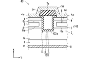
- FIG. 14 is a cross-sectional view schematically illustrating the structure of the semiconductor device 401 according to the fourth embodiment.
- the semiconductor device 401 includes a first layer 1, a laminated semiconductor 102, an insulating gate electrode 103, a fifth layer 8, an interlayer insulating film 9, a source electrode 10, and a drain electrode 11.
- the second layer 2, the third layer 3, and the fourth layer 4 are collectively regarded as the laminated semiconductor 102.
- the insulated gate electrode 103 penetrates the fourth layer 4 and the third layer 3 from the surface 4a in the vertical direction, and extends to the second layer 2.
- the second layer 2 exists between the surface 103a and the surface 1a of the insulated gate electrode 103.
- the insulating gate electrode 103 has a gate insulating film 6 and a gate electrode 7.
- the material of the element of the semiconductor device 401 the material exemplified as the material of the element corresponding to the element of the semiconductor device 101 is adopted.
- the semiconductor device 401 is different from the semiconductor device 201 exemplified by the second embodiment in that the fifth layer 8 does not come into contact with the source electrode 10.
- the side of the semiconductor device 201 far from the first layer 1 of the fifth layer 8 comes into contact with the source electrode 10 (see FIG. 2).
- the fifth layer 8 in the semiconductor device 401 has a surface 8c on the side far from the first layer 1.
- a third layer 3 and a fourth layer 4 are present between the surface 8c and the source electrode 10.
- the position of the surface 8c in the vertical direction is within the range in which the third layer 3 extends in the vertical direction.
- the structure of the semiconductor device 401 is the same as that of the semiconductor device 201 except for the position of the surface 8c in the vertical direction.
- the fifth layer 8 and the insulating gate electrode 103 are located apart from each other in the lateral direction.
- the vertical position of the surface 8a is within the range in which the third layer 3 extends in the vertical direction.
- the electrons that have passed through the fourth layer 4 to the third layer 3 are likely to be diffused in the lateral direction.
- the diffusion increases the current density of the semiconductor device 401.
- the c-plane is adopted as the plane 1a.
- the semiconductor device 401 includes the fifth layer 8 having the surface 8a having the shape as described above, not only the high punch-through resistance is obtained like the semiconductor device 101, but also a large current is used like the semiconductor device 201. Suitable for driving.
- the adoption of the surface 8c of the semiconductor device 401 makes it easy to suppress the punch-through current in the third layer 3 while expanding the region where the fourth layer 4 and the source electrode 10 come into contact with each other, similarly to the surface 8b of the semiconductor device 301.
- the semiconductor device 401 includes the fifth layer 8 having the surface 8c having the shape as described above, not only the high punch-through resistance is obtained as in the semiconductor device 101, but also the source electrode 10 and the source electrode 10 are similarly used in the semiconductor device 301.
- the contact resistance with the laminated semiconductor 102 is small.
- the manufacturing method exemplified by using FIGS. 2 to 10 is adopted.
- the fifth layer 8 is formed by introducing impurities into the laminated semiconductor 102 using the mask 132
- the conditions for introducing impurities are different from those in the manufacturing process of the semiconductor device 101. This is because the positions of the surfaces 8a in the vertical direction are different from each other in the semiconductor devices 101 and 401, and the fifth layer 8 of the semiconductor device 401 has the surface 8c.
- the acceleration energy adopted in ion implantation is adjusted so that the surfaces 8a and 8c are arranged at the above-mentioned positions.
- the acceleration energy used in ion implantation is adjusted so that the fifth layer 8 is formed in contact with the third layer 3 without contacting either the second layer 2 or the fourth layer 4.
- the manufacturing process of the source electrode 10 and the drain electrode 11 in the semiconductor device 401 for example, the manufacturing process of the source electrode 10 and the drain electrode 11 in the semiconductor device 101 is adopted.
- the feature (I) common to the semiconductor devices 101, 201, 301, 401 is expressed by, for example, the following (Ia), (Ib), (Ic), (Id), (Ie).
- the semiconductor devices 101, 201, 301, 401 include a first layer 1, a second layer 2, a third layer 3, a fourth layer 4, a gate electrode 7, a fifth layer 8, a source electrode 10, and a drain electrode 11. including.
- the first layer 1 is a semiconductor having n-type conductivity and has surfaces 1a and 1b facing each other.
- the second layer 2 is a semiconductor having n-type conductivity and is located on the surface 1a.
- the third layer 3 is an n-type or intrinsic semiconductor having a larger bandgap than the second layer 2 and is located on the second layer 2.
- the fourth layer 4 is an n-type semiconductor having a smaller bandgap than the third layer 3, is located on the third layer 3, and has a surface 4a on the opposite side of the third layer 3. Assuming that the band gap of the second layer 2 is the first band gap, the band gap of the third layer 3 is the second band gap, and the band gap of the fourth layer 4 is the third band gap, the second band gap is used. Is larger than the first bandgap.
- the third bandgap is smaller than the second bandgap.
- the source electrode 10 is electrically connected to the fourth layer 4 on the surface 4a.
- the drain electrode 11 is electrically connected to the first layer 1 on the surface 1b.
- the gate electrode 7 is located along the stacking direction X in which the second layer 2, the third layer 3, and the fourth layer 4 are laminated.
- the gate electrode 7 is insulated by, for example, the gate insulating film 6 in any of the second layer 2, the third layer 3, and the fourth layer 4.
- the gate electrode 7 faces the third layer 3 in a second direction different from the stacking direction X, for example, in the lateral direction.
- the fifth layer 8 sandwiches at least the third layer 3 between the fifth layer 8 and the gate electrode 7 in the second direction.
- the fifth layer 8 is a semiconductor in which the conduction band forms a discontinuous interface with the third layer 3, or has no charge that contributes to conduction.
- the second layer 2, the third layer 3, and the fourth layer 4 function as a drift layer, a channel layer, and an electron supply layer, respectively, and the semiconductor devices 101, 201, 301, and 401 all function as so-called vertical trench MOSFETs. Since the conductive type is not p-type in any of the second layer 2, the third layer 3, and the fourth layer 4, the drift layer, the channel layer, and the electron supply layer using the nitride semiconductor, which is difficult to obtain the p-type conductive type, are formed. It will be realized. Generally, the adoption of a nitride semiconductor in a semiconductor device is advantageous from the viewpoint of driving the semiconductor device at a high frequency. The semiconductor devices 101, 201, 301, 401 can be driven at high frequencies.
- the potential is fixed when the third layer 3 which is an n-type conductive type or a true semiconductor is adopted. May not be effective.
- the fifth layer 8 reduces the punch-through current when a high voltage is applied.
- the semiconductor devices 201, 301, 401 are common in that they have the following feature (II) in addition to the feature (I).
- the fifth layer 8 sandwiches the second layer 2 and the third layer 3 between the fifth layer 8 and the first layer 1 in the stacking direction X.
- the effect of the well can be easily obtained. Due to this effect, the electrons that have moved from the channel to the second layer 2 are likely to be diffused in the lateral direction. The diffusion is suitable for driving where a large current is used.
- the semiconductor devices 201, 301, 401 may have further feature (III).
- Both the second layer 2 and the third layer 3 are nitride semiconductors, and the c-plane of the second layer 2 comes into contact with the third layer 3.
- the effect of the two-dimensional electron gas in the second layer 2 close to the third layer 3 can be further easily obtained. This effect is suitable for driving in which a large current is used.
- the semiconductor device 301 has the following feature (IV) in addition to the feature (I) or feature (II).
- the fifth layer 8 approaches the first layer 1 on the first layer 1 side as the distance from the gate electrode 7 increases.
- Feature (IV) is specifically realized by the inclination of the surface 8a, and it does not hinder the movement of electrons diffusing in the direction of the electric field applied to the electrons. Such a configuration is suitable for driving in which a large current is used.
- the semiconductor device 301 may have further features (Va).
- Both the second layer 2 and the third layer 3 are nitride semiconductors, and the c-bar surface of the second layer 2 comes into contact with the third layer 3.
- the semiconductor devices 301 and 401 are common in that they have the following features (VI) in addition to the features (I).
- the fifth layer 8 sandwiches the third layer 3 and the fourth layer 4 between the fifth layer 8 and the source electrode 10 in the stacking direction X. Due to the feature (VI), the region where the fourth layer 4 and the source electrode 10 come into contact with each other is wide, and the contact resistance between the two is small. A small contact resistance causes a small on-resistance of the semiconductor devices 301 and 401.
- the semiconductor device 301 has the following feature (VII) in addition to the feature (I), feature (II), feature (III), feature (IV), feature (Va), or feature (VI).
- the length (thickness) of the fifth layer 8 in the stacking direction X is longer (thicker) as it is separated from the gate electrode 7.
- the withstand voltage of the semiconductor device 301 is high due to the feature (VII).
- the Al composition of the third layer 3 becomes smaller as it approaches the second layer 2 from the center of the third layer 3, and becomes smaller as it approaches the fourth layer 4 from the center of the third layer 3. You may. Alternatively, the closer to the center of the third layer 3, the larger the Al composition of the third layer 3. Such distribution of the Al composition of the third layer 3 reduces the possibility of cracks occurring from the interface between the second layer 2 and the third layer 3 and the interface between the third layer 3 and the fourth layer 4. ..
- each of the semiconductor devices 101, 201, 301, and 401 may have the following characteristics (VIII).
- Each of the semiconductor devices 101, 201, 301, and 401 may have the following features (IX).
- the second layer 2, the third layer 3, and the fourth layer 4 are all GaN or AlGaN, and the Al composition of the third layer 3 is closer to the second layer 2 when viewed from the center of the third layer 3. It is small, and the closer it is to the fourth layer 4 when viewed from the center of the third layer 3, the smaller it is.
- the fifth layer 8 sandwiches at least the second layer 2 between the fifth layer 8 and the first layer 1 in the vertical direction.
- the manufacturing method of the semiconductor device 101 includes the following features (Xa), (Xb), (Xc), (Xd), (Xe), (Xf), (Xg), and (Xh).
- the manufacturing method does not require that these features be carried out in this order.
- a third layer 3 having a second band gap larger than the first band gap and having a conductivity of n-type or a true semiconductor is formed on the second layer 2.
- a fourth semiconductor having a surface 4a on the third layer 3 on the opposite side to the third layer 3, a third bandgap smaller than the second bandgap, and an n-type conductivity. Layer 4 is formed (see FIG. 3).
- a gate electrode 7 that fills the groove 5 via the gate insulating film 6 and a gate insulating film 6 are formed (see FIG. 9).
- (Xf) Ions are injected into the region 42 (see FIG. 9) of the surface 4a away from the region 41, and at least a part of the third layer 3 is electrically inactivated (see FIG. 10). ..
- a source electrode 10 is formed that contacts the surface 4a at a position sandwiched between the (Xg) regions 41 and 42 and does not contact the gate electrode 7.
- the drain electrode 11 is formed on the second surface.
- the manufacturing method may be adopted as a manufacturing method for the semiconductor devices 201, 301, 401.
- the manufacturing method of the semiconductor devices 101, 201, 301 includes the above-mentioned features (Xa), (Xb), (Xc), (Xd), (Xe), (Xg), (Xh), and further features (Xf). It may be provided by substituting the features (XIf1) and (XIf2).
- a groove 14 is formed from a region 42 away from the region 41 of the surface 4a, penetrating the fourth layer 4 and the third layer 3 to reach the second layer 2 and exposing the second layer 2 (FIG. 11). reference).
- the (XIf2) groove 14 is a semiconductor in which the conduction band forms a discontinuous interface with the third layer 3, or has no charge that contributes to conduction (for example, an insulating layer or is electrically inert). Semiconductor) It is filled with the fifth layer 8.
Landscapes
- Junction Field-Effect Transistors (AREA)
Abstract
半導体装置(101)は、n型半導体である第1層(1)上に位置してn型半導体である第2層(2)と、前記第2層上に位置してn型または真性の半導体である第3層(3)と、前記第3層上に位置してn型半導体である第4層(4)と、前記第2層、前記第3層、前記第4層が積層される第1方向に沿って位置して前記第2層、前記第3層、前記第4層のいずれとも絶縁され、前記第1方向とは異なる第2方向において前記第3層と対向するゲート電極(7)と、前記第3層との間において伝導帯が不連続な界面を形成する半導体であるか、または電導に寄与する電荷を有しない第5層(5)とを備える。前記第5層は前記第2方向において前記ゲート電極との間に少なくとも前記第3層を挟む。前記第3層のバンドギャップは前記第2層のバンドギャップおよび前記第4層のバンドギャップのいずれよりも大きい。
Description
本開示は、半導体装置および半導体装置の製造方法に関する。
Si(シリコン)を基材とした半導体装置が公知である。当該半導体装置の構造の例として、GTO(Gate Turn-Off thyristor)やIGBT(Insulated Gate Bipolar Transistor)が挙げられる。これらはいわゆる縦型の構造を有する。縦型の構造を有する半導体装置は、高耐圧および大電流を用いた駆動という要求に対応して、基板の面積あたりの効率を向上させる。オン抵抗と耐圧とのトレードオフの観点からは、従来の半導体装置の性能は、Siの物性定数に起因する限界に迫っている。
例えば特許文献1においては、Siよりも物性定数が良好な化合物半導体を基材とした電界効果トランジスタが提案されている。当該化合物半導体の材質は、例えばSiC(炭化シリコン)、GaN(窒化ガリウム)、AlN(窒化アルミニウム)である。
GaN、AlNによって例示される窒化物半導体は飽和電子速度が大きいので、窒化物半導体を基材とする半導体装置には高周波における良好な駆動が期待される。
Al(アルミニウム)の添加によって窒化物半導体のバンドギャップが変調される。例えば特許文献2においては、このような変調を活用した構造を有する半導体装置が提案される。
2次元電子ガスが誘起されるヘテロ界面は、窒化物半導体を採用して形成され得る。2次元電子ガスは半導体装置の低抵抗化に寄与する。例えば特許文献3においては、このような寄与を活用した構造を有する半導体装置が提案される。
窒化物半導体を基材とする半導体装置において、Siを基材とする半導体装置と同様に、pn接合を障壁に利用した構造を採用することも考えられる。しかし窒化物半導体においてはp型不純物を電気的に活性化させにくい。
例えば窒化物半導体において、Siと同様にイオン注入と熱処理とを用いてp型不純物の電気的な活性化が図られる場合を想定する。この場合には熱処理時に窒化物半導体の表面においてN(窒素)が解離する。このような解離は空孔(いわゆる「N空孔」)を生成し、N空孔がアクセプタ不純物を補償してしまう。
例えば窒化物半導体において、気相エピタキシャル成長法を用いてp型不純物の導入を図る場合には、気相反応において水素が取り込まれる。取り込まれた水素はアクセプタ不純物を終端し、アクセプタ不純物を電気的に不活性にしてしまう(電気的な「不活性化」とも説明され得る)。
窒化物半導体においてp型不純物を電気的に活性化させにくいことは、p型半導体における実効的なアクセプタ不純物濃度を低下させやすい。かかる低下は、pn接合を利用した半導体装置における閾値電圧の制御性、およびパンチスルー電流の抑制という観点において、望ましくない。
窒化物半導体を基材とする半導体装置において、分極障壁を採用することも考えられる。ここにおいて「分極障壁」とは、分極電荷によって誘起される障壁を指す。例えば分極障壁は、Nの電気的陰性度が大きいことに由来する自発分極によって発生することもあるし、ヘテロ界面における格子定数の差に由来するピエゾ分極によって発生することもあるし、自発分極およびピエゾ分極の両方によって発生することもある。例えば窒化物半導体における分極障壁は、Alの添加に起因するバンドギャップの変調によって形成される。
窒化物半導体を基材として分極障壁を利用した半導体装置において、高電圧が印加されたときに流れるパンチスルー電流の抑制は考慮されていなかった。
本開示は上記の問題を解決するためになされたものであり、高いパンチスルー耐性を有する半導体装置、および当該半導体装置の製造方法を提供することを目的とする。
本開示による半導体装置は、導電性がn型の半導体であって、互いに対向する第1面と第2面とを有する第1層と、前記第1面上に位置し、導電性がn型の半導体であって第1バンドギャップを有する第2層と、前記第2層上に位置し、前記第1バンドギャップよりも大きな第2バンドギャップを有し、導電性がn型であるかまたは真性の半導体である第3層と、前記第3層上に位置し、前記第3層と反対側に第3面を有し、前記第2バンドギャップよりも小さな第3バンドギャップを有し、導電性がn型の半導体である第4層と、前記第2面において前記第1層と電気的に接続されるドレイン電極と、前記第3面において前記第4層と電気的に接続されるソース電極と、前記第2層、前記第3層、前記第4層が積層される第1方向に沿って位置し、前記第2層、前記第3層、前記第4層のいずれとも絶縁され、前記第1方向とは異なる第2方向において前記第3層と対向するゲート電極と、前記第2方向において前記ゲート電極との間に少なくとも前記第3層を挟み、前記第3層との間において伝導帯が不連続な界面を形成する半導体であるか、または電導に寄与する電荷を有しない第5層とを備える。
本開示による半導体装置の製造方法は、導電性がn型の半導体であって互いに対向する第1面と第2面とを有する第1層の前記第1面上に、導電性がn型の半導体であって第1バンドギャップを有する第2層を形成し、前記第2層上に、前記第1バンドギャップよりも大きな第2バンドギャップを有し、導電性がn型であるかまたは真性の半導体である第3層を形成し、前記第3層上に、前記第3層と反対側に第3面を有し、前記第2バンドギャップよりも小さな第3バンドギャップを有し、導電性がn型の半導体である第4層を形成し、前記第3面の第1領域から前記第4層および前記第3層を貫通して前記第2層に至り、前記第1層に至らずに前記第2層を露出させる溝(第1溝)を形成し、絶縁膜を介して前記溝(第1溝)を埋めるゲート電極と前記絶縁膜とを形成する。
当該製造方法の第1の態様は、前記第3面のうち前記第1領域から離れた第2領域に対してイオンを注入して、少なくとも前記第3層の一部を電気的に不活性化し、前記第1領域と前記第2領域とに挟まれた位置において前記第3面と接触し、前記ゲート電極と接触しないソース電極を形成し、前記第2面上にドレイン電極を形成する。
当該製造方法の第2の態様は、前記第3面のうち前記第1領域から離れた第2領域から前記第4層および前記第3層を貫通して第2層に至り前記第2層を露出させる第2溝を形成し、前記第2溝を、前記第3層との間において伝導帯が不連続な界面を形成する半導体であるか、または電導に寄与する電荷を有しない層によって埋めることと、前記第1領域と前記第2領域とに挟まれた位置において前記第3面と接触し、前記ゲート電極と接触しないソース電極を形成し、前記第2面上にドレイン電極を形成する。
本開示による半導体装置によれば高いパンチスルー耐性が得られる。本開示による半導体装置の製造方法によれば本開示による半導体装置が得られる。
本開示の目的、特徴、態様、および利点は、以下の詳細な説明と添付図面とによって、より明白となる。
本開示にかかる半導体装置およびその半導体装置の製造方法が、図面を用いて以下の実施の形態において説明される。
本開示にかかる半導体装置およびその半導体装置の製造方法は、これらの実施の形態により限定されるものではなく、その要旨を逸脱しない範囲において適宜に変更されてもよい。図面においては、理解の容易のため、各部材あるいは各部材の縮尺及び縦横比が現実の縮尺及び縦横比と異なる場合があり、図面同士の間においても同様である。
[実施の形態1]
<構造>
図1は実施の形態1にかかる半導体装置101の構造を模式的に例示する断面図である。半導体装置101は、第1層1、第2層2、第3層3、第4層4、第5層8、絶縁ゲート電極103を含む。
<構造>
図1は実施の形態1にかかる半導体装置101の構造を模式的に例示する断面図である。半導体装置101は、第1層1、第2層2、第3層3、第4層4、第5層8、絶縁ゲート電極103を含む。
第1層1、第2層2、第3層3、第4層4はこの順に、図1における例示においては下方から上方へ向かって、積層される。便宜上、第1層1から第4層4へ向かう方向が積層方向Xと表現される。図面において積層方向Xは下方から上方へ向かう方向として図示される。
便宜上、積層方向Xと直交する方向が方向Yと表現される。図面において方向Yは左から右へ向かう方向として図示される。便宜上、積層方向Xおよび積層方向Xと反対の方向の総称として「縦方向」との表現が採用される。このような「縦」の概念はいわゆる縦型の構造における「縦」と整合する。
また「横方向」との表現が、方向Yのみならず、方向Yとは反対の方向をも含めて採用される。
第1層1はn型導電のGaN層である。ここにおいて「n型導電の」は、導電性がn型であることを指す。第1層1の面1aが第2層2に接する。面1aは例えばGa極性を示すc面((0001)面)である。第1層1は第2層2の基板として機能する。
第2層2はn型導電のGaN層である。第2層2は半導体装置101のドリフト層として機能する。第3層3はn型導電のAlbGa(1-b)N層である。第3層3は半導体装置101のチャネル層として機能する。例えばb=0.18が選定される。第4層4はn型導電のGaN層である。第4層4は半導体装置101の電子供給層として機能する。第2層2、第3層3、第4層4は纏まって、積層半導体102として捉えられる。第1層1、第2層2、第3層3、第4層4、積層半導体102はいずれも窒化物半導体である。第1層1は積層半導体102の基板であるといえる。
第3層3のバンドギャップは第2層2のバンドギャップおよび第4層4のバンドギャップのいずれよりも大きい。第4層4のバンドギャップは第3層3のバンドギャップよりも小さい。第3層3と第2層2との間、および第3層3と第4層4との間のいずれにおいても、ヘテロ界面が形成され、分極障壁が発生する。
絶縁ゲート電極103は縦方向において、第4層4の第2層2とは反対側の面4aから、第4層4および第3層3を貫通し、第2層2まで存在する。絶縁ゲート電極103の第1層1に近い方の面103aは面1aと離れる。面1aと面103aとの間には第2層2が存在する。
絶縁ゲート電極103は溝5および面4aにおいて存在する。溝5は積層半導体102において形成され、積層方向Xに向いて開口する。絶縁ゲート電極103の一部が溝5に埋め込まれている、と捉えられる。
絶縁ゲート電極103はゲート絶縁膜6とゲート電極7とを有する。ゲート電極7は横方向において、少なくとも第3層3と対向する。図1の例示においては、ゲート電極7は横方向において、第3層3の他、第4層4と、第2層2の一部とも対向する。
ゲート絶縁膜6はゲート電極7と積層半導体102との間に存在する。面103aはゲート絶縁膜6が積層半導体102と接触する領域の一部である。溝5においてゲート絶縁膜6はゲート電極7を縦方向にも横方向にも覆う。図1の例示においてはゲート電極7は積層方向Xにおいて面4aを覆わない。ゲート電極7の横方向における周囲においてゲート絶縁膜6が面4aに接触する。
ゲート絶縁膜6の材質は例えば酸化ケイ素(SiO2)である。ゲート電極7の材質は例えば多結晶シリコン(poly-Si)である。
第5層8は横方向においてゲート電極7との間に少なくとも第3層3を挟む。例えば第5層8は横方向においてゲート電極7との間に第3層3とゲート絶縁膜6とを挟む。第5層8は横方向において第3層3を挟んで絶縁ゲート電極103と対向する。
半導体装置101においては第5層8が縦方向において、面4aから第4層4および第3層3を貫通し、第2層2まで存在する。第5層8の第1層1に近い方の面8aは面1aと離れる。面1aと面8aとの間には第2層2が存在する。第5層8は縦方向において第1層1との間に少なくとも第2層2を挟む。第5層8は縦方向において少なくとも第2層2を挟んで第1層1と対向する。
第5層8が採用されない構造と比較すると、第5層8は横方向において第3層3を狭める、と捉えられる。この観点で第5層8を狭窄用層ということもできる。
例えば第5層8は、電導に寄与する電荷を有しない層である。第5層8は例えば絶縁層であり、空気であってもよい。第5層8は例えば、電気的な活性化がなされた不純物を有しない半導体である。第5層8の材質が電導に寄与する電荷を有する場合については後述される。
半導体装置101は、層間絶縁膜9と、ソース電極10と、ドレイン電極11とを更に含む。ゲート電極7の積層方向X側の面7aは層間絶縁膜9によって覆われる。図1においては絶縁ゲート電極103は、その積層方向X側において層間絶縁膜9によって覆われる場合が例示される。
図1の例示においては、第4層4を覆うゲート絶縁膜6が層間絶縁膜9によって覆われる。層間絶縁膜9はゲート電極7とソース電極10との間を絶縁する機能を有する。層間絶縁膜9は縦方向において、ゲート絶縁膜6を介して面4aと対向する。面4aのうちゲート絶縁膜6に覆われない部分と、ソース電極10とが接触し、第4層4とソース電極10とが電気的に接続される。図1の例示においては、第5層8および層間絶縁膜9が、その積層方向X側においてソース電極10に覆われる場合が例示される。
ドレイン電極11は第1層1の面1bを覆い、第1層1とドレイン電極11とが電気的に接続される。面1a,1bを除いて考えた第1層1を挟んで、面1aと面1bとが対向する。図1の例示においては、積層方向Xは、面1bから面1aへ向かう方向である。面1aがc面であるとき面1bはN極性を示すcバー面((0001バー)面)である。本実施の形態および以下の実施の形態において「cバー」は通常の表記においては記号「c」に上線が付記される表記を意味し、「1バー」は通常の表記においては記号「1」に上線が付記される表記を意味する。
ソース電極10およびドレイン電極11は、例えば、いずれもTi(チタン)/Al/Ni(ニッケル)/Au(金)の積層構造を有する。ソース電極10においてはTi層が面4aと接触する。ドレイン電極11においてはTi層が面1bと接触する。
半導体装置101は、電子供給層たる第4層4とチャネル層たる第3層3との間に分極障壁を有し、ドリフト層たる第2層2とチャネル層たる第3層3との間に分極障壁を有する。
窒化物半導体においてはp型不純物を活性化させることは難しい。半導体装置101においては導電性がp型である窒化物半導体(以下「p型導電の窒化物半導体」と称す)が採用される必要性がない。かかる必要性の回避は、pn接合を利用した半導体装置と比較して、窒化物半導体を基材とする半導体装置における閾値電圧の制御性(以下「閾値制御性」と称す)を高める。半導体装置101によれば、チャネル層にp型導電の窒化物半導体が用いられなくても、分極障壁を利用した電子電流をスイッチングによって制御することが可能である。
半導体装置101は縦型トレンチMOSFET(Metal-Oxide-Semiconductor Field-Effect Transistor)として機能する。チャネル層にp型導電の窒化物半導体を用いない縦型トレンチMOSFETの動作は、例えば特許文献3において公知であるので、本開示においては省略される。
p型導電の窒化物半導体によって電位を固定する効果は、半導体装置101において得られないかも知れない。かかる効果の有無に依らず、半導体装置101においては高電圧が印加されたときのパンチスルー電流が第5層8によって低減される。
第3層3はチャネル層として機能し、ゲート電極7に近いチャネル層よりも、ゲート電極7から遠いチャネル層においてパンチスルーが発生しやすい。半導体装置101は、第5層8が存在しない半導体装置と比較して、チャネル層として機能する第3層3のうち、パンチスルーが発生しやすい部分が第5層8によって置換された構造を有する。
当該置換は第3層3においてパンチスルーが発生しやすい領域を低減し、パンチスルー電流の低減に寄与する。半導体装置101は、第5層8が存在しない場合と比較して高いパンチスルー耐性を有する。
半導体装置101の特性は、p型導電の窒化物半導体における不純物活性化率に依存する可能性が低い。かかる可能性が低いことは、半導体装置101が閾値制御性に優れることに寄与する。
<緒元の設計>
第2層2、第3層3、第4層4の厚みや組成、ドーピング濃度は半導体装置101に要求される仕様に応じて設計される。
第2層2、第3層3、第4層4の厚みや組成、ドーピング濃度は半導体装置101に要求される仕様に応じて設計される。
例えば第2層2の厚さ(積層方向Xにおける長さ:以下同様)は10μmであり、第3層3の厚さは1μmであり、第4層4の厚さは0.1μmである。これらの膜厚は一例に過ぎない。上記の値以外の膜厚であっても、本開示の趣旨を逸脱しない範囲において任意に選択され得る。これらの膜厚は、半導体装置101の耐圧およびオン抵抗の何れか一方、あるいはこれらの両方に基づく要求に従って適当に選択され得る。
第2層2においてAlaGa(1-a)N層が採用されてもよいし、第4層4においてAlcGa(1-c)N層が採用されてもよい。但し第2層2および第4層4のいずれも、第3層3と比較してAl組成が小さい。例示された組成比に即すると、b>aかつb>cという設定が採用される。
Al組成が異なって(Al組成が0の場合も含め)接合される2種のAlGaN層は、エピタキシャル成長法(例えば有機金属気相成長法(metalorganic vapor phase epitaxy:以下「MOVPE」と称す))を用いて実現される。この場合、当該2種のAlGaN層が接合される界面において、格子定数の不整合に由来してクラックが発生する可能性がある。当該2種のAlGaN層におけるAl組成の相違が大きいほど、2種のAlGaN層の界面からクラックが発生する可能性は高い。
かかるクラックが発生する可能性を低減する観点から、第3層3のAl組成は、第3層3の中央からみて第2層2に近いほど(積層方向Xと反対側に進むほど)小さく、第3層3の中央からみて第4層4に近いほど(積層方向Xに進むほど)小さい。第3層3のAl組成は第3層3の中央に近いほど大きくてもよい。第3層3のAl組成は積層方向Xに沿って均一である必要はない。
AlGaN半導体は、そのAl組成が大きいほど、絶縁破壊電界強度が高い。第2層2におけるAl組成が大きいほど、半導体装置101の耐圧が向上する。AlGaN半導体は、そのAl組成が大きいほど合金散乱による電子移動度が小さく、抵抗率が高い。第2層2におけるAl組成が大きいほど、半導体装置101のオン抵抗が大きい。大電流を用いて半導体装置101を駆動するには、第2層2においてAl組成が小さくされ、半導体装置101のオン抵抗が小さくされる。かかる観点から、実施の形態1においては第2層2がGaN層である(つまりa=0)場合が例示される。
第4層4のAl組成が小さいほど、第4層4とソース電極10とが接合される界面における伝導帯の不連続量は低下する傾向にある。第4層4のAl組成が小さいと、第4層4とソース電極10との間におけるコンタクト抵抗が小さい。かかる観点から、実施の形態1においては第4層4がGaN層である(つまりc=0)場合が例示される。
電子電流を阻止する機能を果たす分極障壁を実現する観点から、分極障壁において伝導帯が不連続となるエネルギーは、室温に対応する熱エネルギー(0.026eV)の例えば10倍以上に設計される。
例えば第3層3と第4層4とが接合される界面における伝導帯の不連続量は0.35eV以上である。かかる不連続量が得られる例として、上述の組成比を用いて言えば、b-c≧0.1である。第4層4がGaN層であるときにはc=0であり、上述において例示されたb=0.18はb-c≧0.1を満足する。
第3層3と第2層2との間にも同様の関係が望まれ、b-a≧0.1である。第2層2がGaN層であるときにはa=0であり、上述において例示されたb=0.18はb-a≧0.1を満足する。
第3層3におけるAlの組成bは1未満である。エピタキシャル成長の途中において格子の不整合に起因したクラックの発生を回避する観点においては、b≦0.8が望ましく、b≦0.5がより望ましい。
上記を纏めるとAl組成a,b,cは、0≦a≦b-0.1、かつ、0≦c≦b-0.1、かつ、b<1(望ましくはb≦0.8、更に望ましくはb≦0.5)を満足する。
積層半導体102にはn型導電の半導体、真性半導体(いわゆるi型)が含まれ得るが、p型導電の半導体が含まれる必要はない。第3層3としてAlGaN層が用いられる場合、真性半導体を意図して作製されてもよい。いわゆるUID(unintentionally doped:意図されずにドーピングされた)半導体が得られるからである。
AlGaN層を成膜する工程において、Siや酸素(O)が不純物となってAlGaN層半導体に取り込まれることにより、弱いn型の導電性を有するAlGaN層が得られる。例えばエピタキシャル成長に用いられる成長炉の内壁から、上述のSiやOが脱離する。AlGaN層を成膜する工程においてN空孔が形成されることによっても、弱いn型の導電性を有するAlGaN層が得られる。
面1aはN極性を示すcバー面であってもよい。このとき、面1bはGa極性を示すc面である。積層半導体102をエピタキシャル成長法によって作製するとき、面4aがGa極性とN極性のいずれを示すかは、面1aがGa極性とN極性のいずれを示すかに依存する。実施の形態1において面1a,4aがGa極性とN極性のいずれを示すかは不問である。
ゲート絶縁膜6の膜厚が大きいとゲート絶縁膜6の絶縁破壊を誘発する電圧は高い。ゲート絶縁膜6の膜厚が大きいと半導体装置101の閾値電圧が高く、ゲート電極7を用いた半導体装置101の制御性が低い。ゲート絶縁膜6の膜厚が小さいと閾値電圧が低く、かつゲート絶縁膜6の絶縁破壊が誘発されやすい。かかる観点から、ゲート絶縁膜6の膜厚は例えば30~100nmに設計される。例えば実施の形態1においてはゲート絶縁膜6の膜厚は50nmである。
ゲート絶縁膜6の材質には、チャネル層として機能する第3層3に選定された窒化物半導体のバンドギャップよりも大きいバンドギャップを有する材質が選定される。ゲート絶縁膜6の電子親和力が小さいと、伝導帯側の不連続量が大きく、ゲート絶縁膜6と第3層3との間の電子障壁が得られやすい。
かかる観点に鑑みて、ゲート絶縁膜6の材質の例として、SiO2、酸化アルミニウム(Al2O3)、窒化ケイ素(Si3N4)、窒化アルミニウム(AlN)、酸化ハフニウム(HfO2)、酸化ランタン(La2O3)、酸化ガドリニウム(Gd2O3)が挙げられる。
ここに例示された材質は全て2元系であるが、これらが2種類以上組み合わさった混晶系や多層の複合膜がゲート絶縁膜6に採用されてもよい。例えば実施の形態1においてはゲート絶縁膜6の材質はSiO2である。
ゲート電極7の材質の例として、リン(P)あるいはホウ素(B)がドーピングされた多結晶シリコンが挙げられる。ゲート電極7の材質として金属が用いられてもよいし、窒化チタン(TiN)が用いられてもよい。ゲート電極7は単層である必要はなく、例えば、金属と多結晶シリコンとの積層構造を有してもよい。
層間絶縁膜9の厚さは、半導体装置101の制御性が考慮されるゲート絶縁膜6ほどには制約されない。例えば層間絶縁膜9の膜厚は半導体装置101に要求される耐圧によって設計される。層間絶縁膜9の膜厚が本開示の趣旨に与える影響は小さい。例えば実施の形態1においては層間絶縁膜9の厚さは100nmであるが、100nmより大きくてもよい。層間絶縁膜9の膜厚は技術的に常識的な範囲において任意に設定してよい。
層間絶縁膜9の材質も、ゲート絶縁膜6の材質と同様に、例えば電子親和力の小さな材質が用いられる。層間絶縁膜9の材質の例として、ゲート絶縁膜6の材質と同様に、先に挙げたSiO2、Al2O3、Si3N4、AlN、HfO2、La2O3、Gd2O3が挙げられる。層間絶縁膜9の材質として酸化ジルコニウム(ZrO2)、酸化ガリウム(Ga2O3)、酸化タンタル(Ta2O3)が用いられてもよい。
ここに例示された材質は全て2元系であるが、これらが2種類以上組み合わさった混晶系や多層の複合膜が層間絶縁膜9に採用されてもよい。例えば実施の形態1においては層間絶縁膜9の材質はSiO2である。
第5層8の抵抗率は、例えば10MΩcm以上である。第5層8の材質が電導に寄与する電荷を有してもよい。第5層8の材質が窒化物半導体である場合について以下に例示する。半導体の抵抗率は半導体のキャリア密度とキャリアの移動度との積に反比例する。キャリア密度を低下させる、キャリア移動度を低下させる、あるいはキャリア密度とキャリア移動度との両方を低下させることが、半導体の抵抗率の増大に寄与する。
深いアクセプタ準位を形成する不純物がドープされた窒化物半導体は、そのキャリア密度が小さく、第5層8として採用できる。当該不純物の例として、鉄(Fe)や炭素(C)がよく知られており、その他にもコバルト(Co)、マンガン(Mn)、バナジウム(V)がある。非晶質構造を有する窒化物半導体は結晶構造のような長距離周期を有さず、キャリアの移動度が小さい。非晶質構造を有する窒化物半導体が、第5層8として採用されてもよい。
第5層8の材質が電導に寄与する電荷を有している場合には、第5層8が積層半導体102との間、特にチャネル層として機能する第3層3との間において、電子伝導を阻害する界面を形成する材質が採用される。電子伝導が阻害されることにより、第4層4から供給された電子が第2層2へ流れる経路には第5層8は含まれない。
当該材質としては、例えば第5層8と第3層3との界面においてヘテロ接合が形成され、当該界面において伝導帯が不連続となる半導体が挙げられる。かかる半導体は例えば、第3層3をAlbGa(1-b)Nを用いて形成したとき、b<dであるAldGa(1-d)Nを用いて形成される。
室温に対応する熱エネルギーが0.026eVであるので、例えば1.0eV以上のエネルギー差によって伝導帯を不連続とする半導体が、第5層8に採用される。後の説明の便宜上、第5層8に採用される半導体を第5層8が第3層3を狭める観点から、当該半導体は「狭窄用半導体」と称される。
ゲート電極7に高い電圧が印加される時には、当該電圧を原因として第3層3とゲート電極7との間に印加される電界も高い。当該電界が考慮され、例えば界面において1.5eV以上のエネルギー差によって伝導帯を不連続とする半導体が、第5層8に採用される。
第5層8と絶縁ゲート電極103との間の横方向における距離が大きいと、第5層8と絶縁ゲート電極103との間の積層半導体102において、パンチスルー電流が発生しやすい可能性がある。かかる観点から、第5層8と絶縁ゲート電極103との間の距離には、好適な範囲が存在することが想定される。
当該範囲、特に当該範囲の上限は、種々の条件、例えば第3層3のAl組成およびゲート電極7に印加される電圧の範囲に応じて予め想定され得る。かかる条件は空乏層が拡がる距離(空乏層の幅)に影響を与え、当該範囲の上限は空乏層の幅に影響される。例えば実施の形態1において当該上限は1μmである。第5層8と絶縁ゲート電極103との間の横方向における距離は1μm以下である。
ソース電極10およびドレイン電極11のいずれも、n型導電の窒化物半導体とオーミック接触する。ソース電極10およびドレイン電極11には、例えば多層構造が採用される。窒化物半導体と接触する層(コンタクト層)の材質として、例えばTi、タンタル(Ta)、V、Alが用いられる。コンタクト層を介して窒化物半導体と接続される層の材質として、例えばニオブ(Nb)、モリブデン(Mo)、Ni、銅(Cu)、白金(Pt)、Auが用いられる。
ソース電極10およびドレイン電極11のいずれもが単層であってもよい。コンタクト抵抗の低減および防蝕によって例示される機能性の発現を期待する場合、当該機能に適した金属が適宜に選択される。
<製造方法>
以下に、半導体装置101の製造方法が、図2から図10を参照して説明される。図2から図10は、実施の形態1にかかる半導体装置101の製造方法を工程順に例示する断面図である。
以下に、半導体装置101の製造方法が、図2から図10を参照して説明される。図2から図10は、実施の形態1にかかる半導体装置101の製造方法を工程順に例示する断面図である。
第1層1の面1a上に積層半導体102が形成されて図2に示される構造が得られる。積層半導体102が形成される前に面1aに対して表面洗浄が実施される。積層半導体102は例えばMOVPEによって形成される。積層半導体102は、面1aから第2層2、第3層3、第4層4の順に積層された構造を有する。この段階においては面4aが露出している(図2)。
面1a上に積層半導体102がエピタキシャル成長する際、面4aには積層半導体102の下地となる面1aの極性が反映される。実施の形態1において面1aにはc面が採用されてもよいし、cバー面が採用されてもよい。
面4a上に誘電膜120が形成されて図3に示される構造が得られる。誘電膜120は第1層1とは反対側において積層半導体102を覆う。誘電膜120の材質は例えばSiO2である。誘電膜120は例えばプラズマ援用化学気相成長法(plasma-enhanced chemical vapor deposition:以下「PECVD」と称す)によって形成される。
誘電膜120が成形されて誘電膜12が得られ、後述する残渣が除去されて図4に示される構造が得られる。誘電膜12は溝5を形成するためのエッチング(後述)におけるマスクとして利用される。誘電膜12は部分的に領域41において面4aを露出させる。
誘電膜120の成形は、例えばレジストパターンをマスクとした誘導結合プラズマ反応性イオンエッチング(inductive coupled plasma-reactive ion etching:以下「ICP-RIE」と称す)による誘電膜120のエッチングによって行われる。当該レジストパターンは、誘電膜120上に形成されたレジストマスク(不図示)に対してフォトリソグラフィを行うことにより得られる。当該フォトリソグラフィにおいては、溝5を形成するためのパターンがレジストマスクに対して転写される。誘電膜12のパターンは、レジストマスクに対して転写されたパターンを反映する。
誘電膜120の材質が、Si系の誘電膜(例えば上記において例示されたSiO2)である場合は、ICP-RIEにおけるエッチングガスの例は、テトラフルオロメタン(CF4)、トリフルオロメタン(CHF3)、六フッ化硫黄(SF6)によって例示されるフッ素系ガスと、酸素との混合ガスである。
誘電膜120のエッチングが完了し、誘電膜12が得られた後、レジストマスクが残渣として存在する可能性がある。酸洗浄と有機洗浄とが併用されて当該残差が除去される。
積層半導体102に対して、誘電膜12がマスクとして利用されるエッチングが行われて溝5が形成され(掘られ)、図5に示される構造が得られる。当該エッチングには例えばICP-RIEが採用される。
積層半導体102の材質が窒化物半導体であるとき、ICP-RIEが採用されて積層半導体102がエッチングされる場合のエッチングガスには、塩素系のガスが採用される。エッチングガスの例は、塩素(Cl2)、三塩化ホウ素(BCl3)、あるいは四塩化ケイ素(SiCl4)である。
積層半導体102がエッチングされる深さ(縦方向の長さ)は、溝5が絶縁ゲート電極103によって埋め込まれることを考慮して設定される。半導体装置101においては絶縁ゲート電極103が縦方向において、面4aから第4層4および第3層3を貫通して第2層2まで存在する。溝5は縦方向において面4aから第4層4および第3層3を貫通して第2層2に至る。溝5は第2層2を露出させる。
上述の例示においては第3層3の厚さは1μmであり、第4層4の厚さは0.1μmであり、両者の合計は1.1μmである。この場合、溝5の深さは1.1μm以上である。積層半導体102がエッチングされる深さは、プロセス尤度を考慮して、例えば1.3μmが目安とされる。
溝5が形成された後、誘電膜12は酸洗浄およびアルカリ洗浄のいずれか一方もしくは両方が用いられて除去される。エッチングによってダメージを受けた積層半導体102の表面(以下「ダメージ層」と仮称)、例えば溝5の内壁も、酸洗浄およびアルカリ洗浄のいずれか一方もしくは両方が用いられて除去される。
誘電膜120として、SiO2によって例示される酸化膜が用いられる場合、誘電膜12の除去には例えばフッ酸(HF)あるいは緩衝フッ酸(BHF)を用いた酸洗浄が採用される。
積層半導体102の材質が窒化物半導体であるとき、ダメージ層は結合強度が低下した窒化物半導体である。ダメージ層の除去には、例えば硫酸過水(sulfuric acid/hydrogen peroxide mixture:SPM)を用いた酸洗浄が採用されてもよいし、例えば水酸化テトラメチルアンモニウム(Tetramethylammonium hydroxide:TMAH)を用いたアルカリ洗浄が採用されてもよい。
酸洗浄およびアルカリ洗浄のいずれにおいても、洗浄液の温度を上昇させることは、反応性を向上させる。洗浄液の温度を過剰に上昇させることはダメージ層以外の積層半導体102へダメージを拡大させる可能性がある。
図5に示される構造から誘電膜12およびダメージ層が除去されて、積層半導体102が露出する部位が清浄化される。当該部位を被覆する絶縁膜60が形成されて図6に示される構造が得られる。絶縁膜60は溝5の形状を反映して積層方向Xに向かって開口する凹部66を有する。
絶縁膜60は後にパターニングされてゲート絶縁膜6として利用される。絶縁膜60の材質には、既述されたゲート絶縁膜6の材質が採用される。
絶縁膜60を形成する手法の例として、原子層堆積法(Atomic layer deposition:以下「ALD」と称す)、PECVD、スパッタリング法が挙げられる。例えばプラズマ状の粒子あるいはスパッタされた粒子が、積層半導体102の露出面へ飛来するとき、これらの粒子が有するエネルギーが低いことは、絶縁膜60と積層半導体102との界面への損傷を低減することに寄与する。かかる観点から、比較的穏やかな形成手法、例えばALDが絶縁膜60を形成する手法に採用される。
ゲート絶縁膜6の膜厚は絶縁膜60の膜厚を反映する。絶縁膜60の溝5に対する段差被覆性(いわゆるステップカバレッジ)が良好である場合を想定し、実施の形態1においては絶縁膜60の膜厚としてゲート絶縁膜6と同様に50nmが採用される。
絶縁膜60が形成された直後に、絶縁膜60の膜質の改善を意図した熱処理を加えてもよい。当該熱処理における環境、例えば温度、雰囲気ガス、圧力は適宜に設計される。実施の形態1において絶縁膜60に例えばSiO2が採用されるとき、例えば摂氏700~1000度の範囲から選択された温度が当該熱処理に採用される。当該範囲から逸脱した温度における熱処理によると、積層半導体102において多結晶が形成される場合が想定される。多結晶においては結晶粒界を介したリーク電流が流れ得る。絶縁膜60は、例えば積層半導体102において多結晶が形成されない条件において、熱処理される。
絶縁膜60の形成後にゲート電極7が形成されて、図7に示される構造が得られる。実施の形態1においては、ゲート電極7は絶縁膜60の凹部66を埋めるが、縦方向において面4aと対向する位置には存在しない場合が例示される。例えば積層方向Xにおける面7aの位置は、絶縁膜60が第4層4とは反対側において露出する面60aの積層方向Xにおける位置と一致する。
溝5は絶縁膜60を介してゲート電極7によって埋められる。例えばゲート電極7の厚さは溝5の厚さと同程度である。実施の形態1においてはゲート電極7の厚さは1.3μmに設計される。
厚いゲート電極7の形成には、堆積レートが高い方法が採用される。例えば絶縁膜60の積層方向X側の全面に、多結晶シリコンが一旦CVD法によって形成される。形成された多結晶シリコンがエッチバックされてゲート電極7が得られる。
例えば絶縁膜60の積層方向X側の全面に、TiNが一旦スパッタリング法によって形成される。形成されたTiNに対してマスクを利用したエッチングを行ってゲート電極7が得られる。当該マスクには、例えばフォトリソグラフィによるパターニングを受けたレジストが採用される。あるいはゲート電極7はリフトオフ法を用いて形成されてもよい。リフトオフ法が採用される場合には、TiN以外の金属がゲート電極7の材質として採用されてもよい。
図7によって示される構造に対して、第1層1とは反対側から絶縁膜90が形成されて、図8に示される構造が得られる。絶縁膜90は絶縁膜60およびゲート電極7を覆う。
絶縁膜90は後にパターニングされて層間絶縁膜9として利用される。絶縁膜90の材質には、既述された層間絶縁膜9の材質が採用される。
層間絶縁膜9はゲート絶縁膜6と比較して膜厚についての制約が緩和される。絶縁膜90が形成される際、絶縁膜60が形成される際よりも、積層半導体102が受ける損傷が考慮される必要性は小さい。絶縁膜60の段差被覆性は、溝5に対する絶縁膜90の段差被覆性よりも深刻性が小さい。かかる事情は絶縁膜60と比較して、絶縁膜90の形成方法の選択肢を拡げる。
例えば絶縁膜90の形成方法には、ALD、PECVD、スパッタリング法のみならず、塗布法やゾルゲル法が採用されてもよい。例えば実施の形態1においてはPECVDにより絶縁膜90が形成される。
図8に示される構造に対して、絶縁膜90の積層方向X側の表面にマスク131が形成される。マスク131は少なくとも溝5を覆う。マスク131は、例えばフォトリソグラフィによるパターニングを受けたレジストによって形成される。
マスク131を用いたエッチング、例えばドライエッチングによって、マスク131に覆われていない絶縁膜60,90が除去される。かかる除去によって絶縁膜60がゲート絶縁膜6へと成形され、絶縁膜90が層間絶縁膜9へと成形されて、図9に示される構造が得られる。層間絶縁膜9は縦方向において少なくとも溝5と対向する。層間絶縁膜9は少なくとも溝5に対して横方向へ広がる。ゲート絶縁膜6は層間絶縁膜9に覆われて面4a上に存在する。絶縁膜60,90が除去された領域において面4aが露出する。
実施の形態1においては絶縁膜60,90のいずれにもSiO2が採用され、面4aを有する第4層4には窒化物半導体が採用される。例えば絶縁膜60,90を除去するためのエッチングガスとしては、誘電膜120のドライエッチングについて説明された、フッ素系ガスと酸素との混合ガスが用いられる。
図9に示される構造に対して例えば公知のアッシング方法が用いられて、マスク131が除去される。少なくとも、層間絶縁膜9の積層方向X側の表面、および層間絶縁膜9の周囲において露出する面4aに、マスク132が形成される(図10参照)。面4aはゲート絶縁膜6およびその周囲に位置するマスク132によって覆われる。図9には、面4aがマスク132によって覆われない領域42が示される。
マスク132の材質として、絶縁膜60,90と同種の物質(例えばSiO2)が用いられたならば、マスク132が除去される際に層間絶縁膜9、ゲート絶縁膜6は損傷もしくは除去される可能性がある。マスク132は、例えばフォトリソグラフィによるパターニングを受けたレジストによって形成される。
積層半導体102へのマスク132を利用した不純物導入によって、第5層8が形成され、図10に示される構造が得られる。不純物導入には例えばイオン注入が採用される。
第5層8はマスク132によって覆われていない領域42(図9参照)において積層半導体102に縦方向に沿って形成される。図10による例示においては第5層8は縦方向において、面4aから、第4層4および第3層3を貫通し、第2層2まで存在する。
積層半導体102への不純物は以下のように導入される。上述の様に第5層8の抵抗率は、例えば10MΩcm以上である。このような抵抗率を得るために用いられる不純物は既に例示された。
エネルギーが高い粒子が半導体に照射されると、当該半導体の結晶性は低下して非晶質な構造へ変化しやすい。非晶質な構造において半導体はキャリアの移動度が小さく、当該半導体の抵抗率は大きい。例えば積層半導体102に上述の不純物のイオンの加速に採用されるエネルギー(いわゆる加速エネルギー)によってイオンが注入され、第5層8が得られる。イオン注入による結晶性の低下は、上述の不純物以外のイオンを用いても期待される。
加速エネルギーを一定としてイオン注入を行うと、不純物の濃度分布が不均一となりやすい。例えば、複数の加速エネルギーを用いた多段注入、傾斜注入は、イオン注入された半導体における不純物濃度分布を均一にしやすい。
傾斜注入の例は、チャネリング軸に沿ったイオン注入である。窒化物半導体においてチャネリング軸には、例えば窒化物半導体のc軸が採用される。チャネリング軸に沿ったイオン注入によると、半導体中のイオンの飛程が伸びやすい。チャネリング軸に沿ったイオン注入は、実施の形態1に沿っていえば、面8aを面1aに近づけやすい。
第5層8を得るために積層半導体102に導入あるいは活性化される不純物の濃度は、例えば1016cm-3以上1021cm-3未満である。
導入された不純物の濃度分布は、熱拡散が採用されて調整されてもよい。かかる熱拡散に採用される熱処理が行われる場合には、不純物が活性化してアクセプタ準位が補償されることが想定される。かかる補償を招来する例として、窒化物半導体に導入される不純物が窒化物半導体においてドナー準位を形成する元素である場合が挙げられる。
例えば実施の形態1においては、Feの4段注入と、摂氏600度の熱処理とが採用される。絶縁ゲート電極103が形成される領域以外の全域を第5層8として形成することは、例えばソース電極10と面4aとの接続を阻む。実施の形態1においてはマスク132が、層間絶縁膜9の周囲において露出する面4aを覆い、層間絶縁膜9の周囲における面4aには第5層8が形成されない構造が例示される。ソース電極10と接続される位置関係が得られるのであれば、面4aが露出する領域は上記の例示に限定されない。
図10に示される構造が得られた後、例えば公知のアッシング方法が用いられて、マスク132が除去される。その後、ソース電極10が少なくとも面4a上に形成され、面1b上にドレイン電極11が形成され、図1に示される半導体装置101が得られる。ソース電極10は領域41,42(それぞれ図4、図9参照)に挟まれた位置において面4aと接触する。ソース電極10はゲート電極7とは、層間絶縁膜9の介在によって、接触しない。
実施の形態1において、ソース電極10は第5層8上にも形成され、ソース電極10は絶縁ゲート電極103を覆って形成される場合が例示される。層間絶縁膜9は、ソース電極10とゲート電極7との接続を阻止する。
実施の形態1においてはソース電極10が、蒸着法によってTi/Al/Ni/Auの積層構造として形成される。ソース電極10のパターニングには、例えばリフトオフ法が採用される。
ソース電極10の膜厚を厚くする場合や段差被覆性を向上させる場合には、例えばスパッタリング法が用いられて金属薄膜が堆積され、ソース電極10が形成される。例えば堆積される対象となる面の全体に、一旦スパッタリングを用いて金属薄膜が堆積してから、当該金属薄膜がパターニングされる。当該パターニングの条件は、例えば堆積された金属薄膜の材質に応じて選択される。
ドレイン電極11もソース電極10と同様に形成され、必要に応じてパターニングされる。
ソース電極10およびドレイン電極11が形成された後に熱処理が実施されてもよい。当該熱処理は、ソース電極10と第4層4との界面における相互拡散を招来する。このような相互拡散は、ソース電極10と第4層4との間における密着力の向上やコンタクト抵抗の低減を招来する。当該熱処理は、ドレイン電極11と第1層1との界面における相互拡散を招来する。このような相互拡散は、ドレイン電極11と第1層1との間における密着力の向上やコンタクト抵抗の低減を招来する。当該熱処理の条件は、ソース電極10およびドレイン電極11に採用される金属に応じて選択される。当該熱処理の条件は更に、既に形成済みの構成要素への影響が考慮されてもよい。例えば第5層8が狭窄用半導体によって形成されるとき、狭窄用半導体が有する不純物が電気的に活性化されないことを企図して、当該熱処理における温度は摂氏700度未満に選定される。
第5層8が形成される際にイオン注入が採用される場合、導入される不純物元素と熱処理の条件との組合せは、第5層8における不純物の分布状況や再結晶化に影響を及ぼす可能性がある。
<変形>
実施の形態1は、第5層8を形成する手法を、積層半導体102への不純物導入に限定しない。図11は半導体装置101の製造方法の変形を例示する断面図である。
実施の形態1は、第5層8を形成する手法を、積層半導体102への不純物導入に限定しない。図11は半導体装置101の製造方法の変形を例示する断面図である。
例えば、図9によって示される構造に対し、領域42において、積層半導体102が第2層2が露出するまで除去されて、図11に例示される構造が得られる。当該除去には、例えばマスク132を用いたドライエッチングが採用される。当該ドライエッチングにより、横方向において第3層3、第4層4を露出させ、縦方向および横方向に第2層2を露出させる溝14が形成される。
溝14を埋める第5層8が形成されて、図1に例示される半導体装置101が得られる。この場合の第5層8には公知の絶縁材が採用されてもよい。あるいは溝14において、狭窄用半導体として窒化物半導体がエピタキシャル成長して溝14を埋め、第5層8が形成されてもよい。当該エピタキシャル成長には例えばMOVPEが採用され、上述した窒化物半導体中において深いアクセプタ準位を形成する元素の1種以上が不純物としてドーピングされる。溝14において狭窄用半導体がCVD法によって堆積されて第5層8が得られても良い。あるいは第5層8に空気が採用される場合には、溝14を埋める必要はない。
[実施の形態2]
<構造>
図12は実施の形態2にかかる半導体装置201の構造を模式的に例示する断面図である。半導体装置201は、第1層1と、積層半導体102と、絶縁ゲート電極103と、第5層8と、層間絶縁膜9と、ソース電極10と、ドレイン電極11とを含む。
<構造>
図12は実施の形態2にかかる半導体装置201の構造を模式的に例示する断面図である。半導体装置201は、第1層1と、積層半導体102と、絶縁ゲート電極103と、第5層8と、層間絶縁膜9と、ソース電極10と、ドレイン電極11とを含む。
半導体装置201においても半導体装置101と同様に、第2層2、第3層3、第4層4が纏まって積層半導体102として捉えられる。半導体装置201においても半導体装置101と同様に、絶縁ゲート電極103は縦方向において、面4aから第4層4および第3層3を貫通し、第2層2まで存在する。絶縁ゲート電極103の面103aと面1aとの間には第2層2が存在する。半導体装置201においても半導体装置101と同様に、絶縁ゲート電極103はゲート絶縁膜6とゲート電極7とを有する。
半導体装置201は実施の形態1において例示された半導体装置101と、第5層8の面8aの積層方向Xにおける位置のみ相違する。半導体装置201においては面8aと面1aとの間には第2層2のみならず第3層3も存在する。半導体装置201においては第5層8が縦方向において、面4aから第4層4を貫通し、第3層3まで存在する。
半導体装置201において第5層8は、縦方向において第1層1との間に第2層2のみならず第3層3をも挟む。半導体装置201において第5層8は、縦方向において第2層2のみならず第3層3をも挟んで第1層1と対向する。
半導体装置101において、面8aの縦方向における位置は第2層2が縦方向に広がる範囲にある。半導体装置201において、面8aの縦方向における位置は第3層3が縦方向に広がる範囲にある。
面8aの縦方向における位置以外においては、半導体装置201の構造は半導体装置101と共通する。例えば半導体装置101,201のいずれにおいても、第5層8と絶縁ゲート電極103とは横方向において互いに離れて位置する。半導体装置201が有する要素の材質には、半導体装置101が有する当該要素に対応した要素の材質として例示された材質が採用される。
チャネル層として機能する第3層3におけるパンチスルー電流の抑制という観点からは、ドリフト層として機能する第2層2まで第5層8が到達する必要はない。第5層8の抵抗率が高いほど、面8aの位置は浅くても、例えば面8aが縦方向において第2層2から離れても、パンチスルー電流は抑制されやすい。
半導体装置101,201のいずれにおいても、ゲート電極7に印加される電圧が制御されて第3層3にチャネルが形成されると、第4層4から供給された電子がチャネルを通過する。チャネルを通過した電子は第2層2内を拡散してドレイン電極11へ向かう。
実施の形態1において説明されたように、第2層2と第3層3との間にはヘテロ界面が形成される。ヘテロ界面の第2層2側の領域には、2次元の量子井戸が形成される可能性が高い。当該量子井戸が形成される場合、チャネルを通過した電子は当該量子井戸に到達する。半導体装置201において第5層8は、量子井戸に到達した電子が横方向(ここにおいては絶縁ゲート電極103から離れる向き)に拡散することを妨げない。
特に、第3層3に対して第2層2のc面(これはGa極性を示す)が接する場合、第2層2と第3層3との間に形成されるヘテロ界面の第2層2側の領域において高濃度のキャリアが誘起される可能性が高い。当該キャリアは第2層2および第3層3のそれぞれにおける自発分極及びピエゾ分極によって発生する2次元電子ガスによって実現される。半導体装置201における面8aは半導体装置101における面8aと比較して第3層3と第2層2との間のヘテロ界面を狭めず、2次元電子ガスの誘起を妨げにくい。
半導体装置201によれば、第4層4から第3層3を通過してきた電子は、2次元量子井戸の効果、あるいは2次元量子井戸および2次元電子ガスによって、横方向へ拡散されやすい。このような横方向への拡散により、第2層2は電流拡散層(Current Spreading Layer)として機能するともいえる。かかる電子の拡散は、半導体装置201の電流密度を高める。半導体装置201は半導体装置101と同様に高いパンチスルー耐性を得るほか、動作するときの電流密度が高く、大電流が用いられる駆動に適する。
<製造方法>
半導体装置201の製造には例えば、半導体装置101と同様に、図2から図10を用いて例示された製造方法が採用される。積層半導体102へのマスク132を利用した不純物導入によって、第5層8が形成される際、不純物導入の条件が半導体装置101の製造工程とは異なる。面8aの縦方向における位置が半導体装置101,201は互いに異なるからである。例えばイオン注入において採用される加速エネルギーは、半導体装置101における不純物導入よりも、半導体装置201における不純物導入の方が低い。
半導体装置201の製造には例えば、半導体装置101と同様に、図2から図10を用いて例示された製造方法が採用される。積層半導体102へのマスク132を利用した不純物導入によって、第5層8が形成される際、不純物導入の条件が半導体装置101の製造工程とは異なる。面8aの縦方向における位置が半導体装置101,201は互いに異なるからである。例えばイオン注入において採用される加速エネルギーは、半導体装置101における不純物導入よりも、半導体装置201における不純物導入の方が低い。
半導体装置201におけるソース電極10、ドレイン電極11の製造工程は、例えば半導体装置101におけるソース電極10、ドレイン電極11の製造工程と同様である。
実施の形態1の変形において説明されたように、実施の形態2においても第5層8の形成に先だって溝14が形成されてもよい。但し実施の形態2における溝14は、横方向において第4層4を露出させ、縦方向および横方向に第3層3を露出させる。例えば実施の形態1と同様に、溝14の形成にはドライエッチングが採用される。但し、半導体装置201におけるドライエッチングの条件は、半導体装置101におけるドライエッチングの条件とは異なる。面8aの縦方向の位置が半導体装置101,201は互いに異なるからである。
実施の形態2においても、例えば実施の形態1の変形と同様に、公知の絶縁材、あるいはエピタキシャル成長によって得られた窒化物半導体によって溝14を埋めて第5層8が形成される。第5層8として空気が採用される場合には溝14を埋める必要はない。
面1a上に積層半導体102がエピタキシャル成長する際、積層半導体102の下地となる面1aの極性が、第3層3と第2層2との間に形成されるヘテロ界面の第2層2側に反映される。上述の2次元電子ガスの利用が企図される場合には面1aにc面が採用される。
[実施の形態3]
<構造>
図13は実施の形態3にかかる半導体装置301の構造を模式的に例示する断面図である。半導体装置301は、第1層1と、積層半導体102と、絶縁ゲート電極103と、第5層8と、層間絶縁膜9と、ソース電極10と、ドレイン電極11とを含む。
<構造>
図13は実施の形態3にかかる半導体装置301の構造を模式的に例示する断面図である。半導体装置301は、第1層1と、積層半導体102と、絶縁ゲート電極103と、第5層8と、層間絶縁膜9と、ソース電極10と、ドレイン電極11とを含む。
半導体装置301においても半導体装置101と同様に、第2層2、第3層3、第4層4が纏まって積層半導体102として捉えられる。半導体装置301においても半導体装置101と同様に、絶縁ゲート電極103は縦方向において、面4aから第4層4および第3層3を貫通し、第2層2まで存在する。絶縁ゲート電極103の面103aと面1aとの間には第2層2が存在する。半導体装置301においても半導体装置101と同様に、絶縁ゲート電極103はゲート絶縁膜6とゲート電極7とを有する。半導体装置301が有する要素の材質には、半導体装置101が有する当該要素に対応した要素の材質として例示された材質が採用される。
半導体装置301は実施の形態1によって例示された半導体装置101および実施の形態2によって例示された半導体装置201のいずれとも、第5層8の縦方向における長さ(厚さ)が、絶縁ゲート電極103から離れる程長い(厚い)点において相違する。
半導体装置101,201,301のいずれにおいても、それらが駆動される際にはゲート電極7へ印加される電圧が制御されて絶縁ゲート電極103から積層半導体102へ空乏層が延びる。当該空乏層は積層半導体102に発生する電界を保持する。この電界を保持する空乏層の機能は、絶縁ゲート電極103から遠い位置ほど低下する。このような電界を保持する機能の低下は、積層半導体102の損傷を招来しやすい。絶縁ゲート電極103から離れる程、縦方向における厚さが厚い第5層8が採用されることにより、かかる損傷は回避されやすい。かかる回避は半導体装置301の耐圧を向上させる。
図13によって例示される構造において面8aは、絶縁ゲート電極103から離れるに従って第1層1に近づき、縦方向に対しても横方向に対しても傾斜を有する。実施の形態2において説明された2次元電子ガス、2次元量子井戸による電子の横方向への拡散が小さいとき、第2層2を移動する電子は電界に応じて拡散する。
電子に印加される電界の方向は、第5層8の存在により、第1層1から第3層3に向かうにつれて絶縁ゲート電極103へ近づく傾斜を呈する。当該電界の方向を反映し、第2層2を移動する電子は第1層1に向かうにつれて絶縁ゲート電極103から離れる方向に拡散する。半導体装置301における面8aの傾斜は当該方向へ拡散する電子の移動を妨げにくい。
このような面8aの傾斜は、2次元電子ガスによる電子の横方向への拡散が小さい場合、例えば第3層3に対して第2層2のcバー面(これはN極性を示す)が接する場合に採用されてもよい。
半導体装置301は、上述のような形状を呈する面8aを有する第5層8を含むので、半導体装置201と同様に高いパンチスルー耐性を得て、動作するときの電流密度が高い。
図13に例示される構造の面8aは、第2層2が縦方向において広がる範囲においても存在する。面8aの横方向の位置には、面8aと面1aとの間に第3層3が存在せず第2層2が存在する位置を含む。この観点においては半導体装置101,301の面8aは共通する特徴を有する。
図13に例示される構造の面8aは、横方向において絶縁ゲート電極103に最も近い位置において、第3層3が縦方向において広がる範囲に位置し、面8aと面1aとの間には第2層2のみならず第3層3も存在する。この観点においては半導体装置201,301の面8aは共通する特徴を有する。
面8aの全体が縦方向に存在する位置は、半導体装置101と同様に第2層2が縦方向において広がる範囲にあってもよいし、半導体装置201と同様に第3層3が縦方向において広がる範囲にあってもよい。第3層3に対して第2層2のc面が接する場合には、面8aの全体が縦方向に存在する位置が、第3層3が縦方向において広がる範囲にあることによって、2次元電子ガスの利点が得られやすい。
第5層8が第1層1から遠い方に有する面8bは、絶縁ゲート電極103から離れるに従って第1層1から遠ざかる傾斜を呈する。第5層8は面8bよりも絶縁ゲート電極103から離れた位置においてソース電極10と接触する。
半導体装置301においては面8bが採用されるので、第4層4とソース電極10とが接触する領域は、半導体装置101,201と比較して広い。半導体装置301においては第3層3におけるパンチスルー電流の抑制が得られながら、第4層4とソース電極10との間のコンタクト抵抗が小さい。小さなコンタクト抵抗は小さなオン抵抗を招来する。
図13においては、面8bの縦方向における位置が、第3層3が縦方向において広がる範囲と第4層4が縦方向において広がる範囲との両方に跨った形状が例示される。
面8bの全体が縦方向に存在する位置は、第3層3が縦方向において広がる範囲にあってもよい。このとき更に第5層8がソース電極10から離れてもよい。
図13における例示においては面8a,8bの形状は平面状であって断面視において直線状に現れる。面8a,8bの形状は、断面視において曲線状であってもよい。
積層半導体102に形成される等電位面が断面視において現れる曲線と、面8a,8bが断面視において現れる曲線とが直交することは、面8a,8bが積層半導体102における電界の方向に沿う観点において好適である。但し等電位面はゲート電極7、ソース電極10、ドレイン電極11のそれぞれに印加される電圧に依存するので、形状が固定された第5層8において上記直交が常に実現されるとは限らない。
半導体装置301は、上述のような形状を呈する面8bを有する第5層8を含むので、半導体装置101と同様に高いパンチスルー耐性を得るのみならず、オン抵抗が小さい。
<製造方法>
半導体装置301の製造には例えば、半導体装置101と同様に、図2から図10を用いて例示された製造方法が採用される。積層半導体102へのマスク132を利用した不純物導入によって、第5層8が形成される際、不純物導入の条件が半導体装置101の製造工程とは異なる。面8aの縦方向における位置が半導体装置101,301は互いに異なるからである。また半導体装置101とは異なって、半導体装置301の第5層8はソース電極10と離れる面8bを有するからである。
半導体装置301の製造には例えば、半導体装置101と同様に、図2から図10を用いて例示された製造方法が採用される。積層半導体102へのマスク132を利用した不純物導入によって、第5層8が形成される際、不純物導入の条件が半導体装置101の製造工程とは異なる。面8aの縦方向における位置が半導体装置101,301は互いに異なるからである。また半導体装置101とは異なって、半導体装置301の第5層8はソース電極10と離れる面8bを有するからである。
例えば積層半導体102へ、縦方向に対して傾斜する方向に入射するイオン注入を行って、面8a,8bを有する第5層8が形成される。例えば第1層1、積層半導体102、絶縁ゲート電極103、層間絶縁膜9、マスク132が形成された状態において、第1層1を自転させ、あるいは公転させ、あるいは自転および公転させてイオン注入が行われて、第5層8が形成される。縦方向に平行なイオン注入が伴われて第5層8が形成されてもよい。
イオン注入の積層半導体102に対する傾斜角は、マスク132の厚さおよびマスク132が横方向において積層半導体102(より具体的には面4a)を露出させる長さ(幅)に依存して決定される設計事項である。
実施の形態1の<変形>において説明されたように、実施の形態3においても第5層8の形成に先だって溝14が形成されてもよい。例えば実施の形態1と同様に、溝14の形成にはドライエッチングが採用される。但し、ドライエッチングの条件が半導体装置101の製造工程とは異なる。本実施の形態における溝14は、面8a,8bの形状に反映される形状を有するからである。
例えば積層半導体102へ、縦方向に対して傾斜する方向に入射する粒子を採用したドライエッチングによって溝14が形成される。例えば当該ドライエッチングにおいて第1層1の自転および公転の一方または両方が採用される。
半導体装置301におけるソース電極10、ドレイン電極11の製造工程は、例えば半導体装置101におけるソース電極10、ドレイン電極11の製造工程と同様である。
実施の形態3においても、例えば実施の形態1の変形と同様に、公知の絶縁材、あるいはエピタキシャル成長によって得られた窒化物半導体によって溝14を埋めて第5層8が形成される。あるいは第5層8に空気が採用される場合には、溝14を埋める必要はない。
[実施の形態4]
<構造>
図14は実施の形態4にかかる半導体装置401の構造を模式的に例示する断面図である。半導体装置401は、第1層1と、積層半導体102と、絶縁ゲート電極103と、第5層8と、層間絶縁膜9と、ソース電極10と、ドレイン電極11とを含む。
<構造>
図14は実施の形態4にかかる半導体装置401の構造を模式的に例示する断面図である。半導体装置401は、第1層1と、積層半導体102と、絶縁ゲート電極103と、第5層8と、層間絶縁膜9と、ソース電極10と、ドレイン電極11とを含む。
半導体装置401においても半導体装置101と同様に、第2層2、第3層3、第4層4が纏まって積層半導体102として捉えられる。半導体装置401においても半導体装置101と同様に、絶縁ゲート電極103は縦方向において、面4aから第4層4および第3層3を貫通し、第2層2まで存在する。絶縁ゲート電極103の面103aと面1aとの間には第2層2が存在する。半導体装置401においても半導体装置101と同様に、絶縁ゲート電極103はゲート絶縁膜6とゲート電極7とを有する。半導体装置401が有する要素の材質には、半導体装置101が有する当該要素に対応した要素の材質として例示された材質が採用される。
半導体装置401は、実施の形態2によって例示された半導体装置201と、第5層8がソース電極10と接触しない点において相違する。半導体装置201における第5層8の第1層1から遠い側はソース電極10と接触する(図2参照)。半導体装置401における第5層8は、第1層1から遠い側に面8cを有する。面8cとソース電極10との間には第3層3および第4層4が存在する。半導体装置401において、面8cの縦方向における位置は第3層3が縦方向に広がる範囲にある。
面8cの縦方向における位置以外においては、半導体装置401の構造は半導体装置201と共通する。例えば半導体装置201,401のいずれにおいても、第5層8と絶縁ゲート電極103とは横方向において互いに離れて位置する。
半導体装置401においても、半導体装置201と同様に、面8aの縦方向の位置は第3層3が縦方向に広がる範囲にある。半導体装置401によれば、半導体装置201と同様に、第4層4から第3層3を通過してきた電子が横方向に拡散されやすい。当該拡散は半導体装置401の電流密度を高める。第2層2における2次元電子ガスの利用が企図される場合には、面1aにc面が採用される。
半導体装置401は、上述のような形状を呈する面8aを有する第5層8を含むので、半導体装置101と同様に高いパンチスルー耐性を得るのみならず、半導体装置201と同様に大電流を用いた駆動に適する。
半導体装置401の面8cの採用は、半導体装置301の面8bと同様に、第4層4とソース電極10とが接触する領域を広げつつ、第3層3におけるパンチスルー電流を抑制しやすい。
半導体装置401は、上述のような形状を呈する面8cを有する第5層8を含むので、半導体装置101と同様に高いパンチスルー耐性を得るのみならず、半導体装置301と同様にソース電極10と積層半導体102との間の接触抵抗が小さい。
<製造方法>
半導体装置401の製造には例えば、半導体装置101と同様に、図2から図10を用いて例示された製造方法が採用される。積層半導体102へのマスク132を利用した不純物導入によって、第5層8が形成される際、不純物導入の条件が半導体装置101の製造工程とは異なる。面8aの縦方向における位置が半導体装置101,401は互いに異なり、半導体装置401の第5層8は面8cを有するからである。
半導体装置401の製造には例えば、半導体装置101と同様に、図2から図10を用いて例示された製造方法が採用される。積層半導体102へのマスク132を利用した不純物導入によって、第5層8が形成される際、不純物導入の条件が半導体装置101の製造工程とは異なる。面8aの縦方向における位置が半導体装置101,401は互いに異なり、半導体装置401の第5層8は面8cを有するからである。
例えばイオン注入において採用される加速エネルギーが調整されて、面8a,8cを上述の位置に配置される。例えばイオン注入において採用される加速エネルギーが調整されて、第5層8が第2層2および第4層4のいずれにも接触せずに第3層3に接触して形成される。
半導体装置401におけるソース電極10、ドレイン電極11の製造工程には、例えば半導体装置101におけるソース電極10、ドレイン電極11の製造工程が採用される。
[複数の実施の形態に共通の特徴と個別の特徴]
半導体装置101,201,301,401に共通する特徴(I)は、例えば以下の(Ia),(Ib),(Ic),(Id),(Ie)に分けて表現される。
半導体装置101,201,301,401に共通する特徴(I)は、例えば以下の(Ia),(Ib),(Ic),(Id),(Ie)に分けて表現される。
(Ia)半導体装置101,201,301,401は、第1層1、第2層2、第3層3、第4層4、ゲート電極7、第5層8、ソース電極10、ドレイン電極11を含む。
(Ib)第1層1は導電性がn型の半導体であって、互いに対向する面1a,1bを有する。第2層2は導電性がn型の半導体であって、面1a上に位置する。第3層3は導電性がn型であるかまたは真性の半導体であって第2層2よりもバンドギャップが大きく、第2層2上に位置する。第4層4は導電性がn型の半導体であって第3層3よりもバンドギャップが小さく、第3層3上に位置し、第3層3と反対側に面4aを有する。第2層2が有するバンドギャップを第1バンドギャップとし、第3層3が有するバンドギャップを第2バンドギャップとし、第4層4が有するバンドギャップを第3バンドギャップとすると、第2バンドギャップは第1バンドギャップよりも大きい。第3バンドギャップは第2バンドギャップよりも小さい。
(Ic)ソース電極10は、面4aにおいて第4層4と電気的に接続される。ドレイン電極11は、面1bにおいて第1層1と電気的に接続される。
(Id)ゲート電極7は第2層2、第3層3,第4層4が積層される積層方向Xに沿って位置する。ゲート電極7は第2層2、第3層3、第4層4のいずれとも、例えばゲート絶縁膜6によって絶縁される。ゲート電極7は積層方向Xとは異なる第2方向、例えば横方向において第3層3と対向する。
(Ie)第5層8は第2方向においてゲート電極7との間に少なくとも第3層3を挟む。第5層8は、第3層3との間において伝導帯が不連続な界面を形成する半導体であるか、または電導に寄与する電荷を有していない。
特徴(Ia),(Ib),(Ic),(Id)は、下記の作用あるいは効果を招来する。第2層2、第3層3、第4層4がそれぞれドリフト層、チャネル層、電子供給層として機能し、半導体装置101,201,301,401はいずれもいわゆる縦型トレンチMOSFETとして機能する。第2層2、第3層3、第4層4のいずれも導電型がp型ではないので、p型の導電型を得にくい窒化物半導体を用いたドリフト層、チャネル層、電子供給層が実現される。一般に半導体装置において窒化物半導体が採用されることは、高周波において半導体装置が駆動される観点において有利である。半導体装置101,201,301,401は高周波において駆動され得る。
特徴(Ie)により、第5層8が存在しない場合と比較して、第3層3においてパンチスルーしやすい位置が第5層8によって置換された構造が得られる。かかる構造を有することにより、半導体装置101,201,301,401はいずれも高いパンチスルー耐性を有する。
導電型がp型の半導体である第3層3が採用される場合と比較すると、導電型がn型、もしくは真性の半導体である第3層3が採用される場合には、その電位を固定する効果がないかも知れない。半導体装置101,201,301,401においては第5層8によって、高電圧が印加されたときのパンチスルー電流が低減される。
半導体装置201,301,401は、特徴(I)に加えて、下記の特徴(II)を有する点において共通する。
(II)第5層8は積層方向Xにおいて第1層1との間に第2層2および第3層3を挟む。
特徴(II)により、第5層8が積層方向Xにおいて第1層1との間に第3層3を挟まない場合と比較して、第3層3に近い第2層2における2次元量子井戸の効果が得られやすい。当該効果により、チャネルから第2層2へ移動してきた電子が横方向に拡散されやすい。当該拡散は大電流が用いられる駆動に適する。
半導体装置201,301,401は、更に特徴(III)を有する場合がある。
(III)第2層2および第3層3のいずれもが窒化物半導体であって、第2層2のc面が第3層3に接触する。
特徴(III)により、第3層3に近い第2層2における2次元電子ガスの効果も更に得られやすい。当該効果は大電流が用いられる駆動に適する。
半導体装置301は、特徴(I)または特徴(II)に加えて、下記の特徴(IV)を有する。
(IV)第5層8はその第1層1側において、ゲート電極7から離れるに従って第1層1に近づく。
特徴(IV)は具体的には面8aの傾斜によって実現され、電子に印加される電界の方向へ拡散する電子の移動を妨げにくい。かかる構成は大電流が用いられる駆動に適する。
半導体装置301は、更に特徴(Va)を有する場合がある。
(Va)第2層2および第3層3のいずれもが窒化物半導体であって、第2層2のcバー面が第3層3に接触する。
特徴(Va)によって第3層3に近い第2層2における2次元電子ガス、2次元量子井戸による電子の横方向へ拡散が小さくても、特徴(IV)による効果は妨げられにくい。
半導体装置301,401は特徴(I)に加えて、下記の特徴(VI)を有する点において共通する。
(VI)第5層8は積層方向Xにおいてソース電極10との間に第3層3および第4層4を挟む。特徴(VI)により、第4層4とソース電極10とが接触する領域が広く、両者間のコンタクト抵抗が小さい。小さなコンタクト抵抗は半導体装置301,401の小さなオン抵抗を招来する。
半導体装置301は、特徴(I)、特徴(II)、特徴(III)、特徴(IV)、特徴(Va)、または特徴(VI)に加えて、下記の特徴(VII)を有する。
(VII)第5層8の積層方向Xにおける長さ(厚さ)が、ゲート電極7から離れる程長い(厚い)。特徴(VII)によって半導体装置301の耐圧は高い。
半導体装置101において説明されたように、第3層3のAl組成は、第3層3の中央から第2層2に近づくほど小さく、第3層3の中央から第4層4に近づくほど小さくてもよい。あるいは、第3層3の中央に近いほど第3層3のAl組成が大きくてもよい。このような第3層3のAl組成の分布は、第2層2と第3層3との界面、および第3層3と第4層4との界面からクラックが発生する可能性を小さくする。
半導体装置101,201,301,401は、いずれも共通して積層半導体102を採用するので、いずれについても下記の特徴(VIII)を有してもよい。半導体装置101,201,301,401のいずれについても下記の特徴(IX)を有してもよい。
(VIII)第2層2、第3層3、第4層4はいずれもGaNもしくはAlGaNであり、第3層3のAl組成は、第3層3の中央からみて第2層2に近いほど小さく、第3層3の中央からみて第4層4に近いほど小さい。(IX)第5層8は縦方向において第1層1との間に少なくとも第2層2を挟む。
例えば半導体装置101の製造方法は以下の特徴(Xa)、(Xb)、(Xc)、(Xd)、(Xe)、(Xf)、(Xg)、(Xh)を備えると説明され得る。但し、当該製造方法は、これらの特徴がこの順に実行されることを必須とはしない。
(Xa)導電性がn型の半導体であって互いに対向する面1a,1bを有する第1層1の面1a上に、導電性がn型の半導体であって第1バンドギャップを有する第2層2が形成される。
(Xb)第2層2上に、第1バンドギャップよりも大きな第2バンドギャップを有し、導電性がn型であるかまたは真性の半導体である第3層3が形成される。
(Xc)第3層3上に、第3層3と反対側に面4aを有し、第2バンドギャップよりも小さな第3バンドギャップを有し、導電性がn型の半導体である第4層4が形成される(図3参照)。
(Xd)面4aの領域41(図4参照)から第4層4および第3層3を貫通して第2層2に至り、第1層1に至らずに第2層2を露出させる溝5が形成される(図5参照)。
(Xe)ゲート絶縁膜6を介して溝5を埋めるゲート電極7と、ゲート絶縁膜6とが形成される(図9参照)。
(Xf)面4aのうち領域41から離れた領域42(図9参照)に対してイオンを注入して、少なくとも第3層3の一部が電気的に不活性化される(図10参照)。
(Xg)領域41,42に挟まれた位置において面4aと接触し、ゲート電極7と接触しないソース電極10が形成される。
(Xh)前記第2面上にドレイン電極11が形成される。
当該製造方法は半導体装置201,301,401の製造方法として採用されてもよい。
半導体装置101,201,301の製造方法は、上記特徴(Xa)、(Xb)、(Xc)、(Xd)、(Xe)、(Xg)、(Xh)を備え、更に特徴(Xf)を特徴(XIf1)、(XIf2)に置き換えて備えてもよい。
(XIf1)面4aのうち領域41から離れた領域42から第4層4および第3層3を貫通して第2層2に至り第2層2を露出させる溝14が形成される(図11参照)。
(XIf2)溝14が、第3層3との間において伝導帯が不連続な界面を形成する半導体であるか、または電導に寄与する電荷を有しない(例えば絶縁層、あるいは電気的に不活性な半導体)第5層8によって埋められる。
上述された各実施の形態を自由に組み合わせたり、各実施の形態を適宜、変形、省略することが可能である。
本開示は詳細に説明されたが、上記した説明は、すべての局面において、例示であって、限定的なものではない。例示されていない無数の変形例が想定され得るものと解される。
1 第1層、1a,1b,4a 面、2 第2層、3 第3層、4 第4層、5,14 溝、7 ゲート電極、8 第5層、10 ソース電極、11 ドレイン電極、41,42 領域、101,201,301,401 半導体装置、X 積層方向、Y 方向。
Claims (11)
- 導電性がn型の半導体であって、互いに対向する第1面と第2面とを有する第1層と、
前記第1面上に位置し、導電性がn型の半導体であって第1バンドギャップを有する第2層と、
前記第2層上に位置し、前記第1バンドギャップよりも大きな第2バンドギャップを有し、導電性がn型であるかまたは真性の半導体である第3層と、
前記第3層上に位置し、前記第3層と反対側に第3面を有し、前記第2バンドギャップよりも小さな第3バンドギャップを有し、導電性がn型の半導体である第4層と、
前記第2面において前記第1層と電気的に接続されるドレイン電極と、
前記第3面において前記第4層と電気的に接続されるソース電極と、
前記第2層、前記第3層、前記第4層が積層される第1方向に沿って位置し、前記第2層、前記第3層、前記第4層のいずれとも絶縁され、前記第1方向とは異なる第2方向において前記第3層と対向するゲート電極と、
前記第2方向において前記ゲート電極との間に少なくとも前記第3層を挟み、前記第3層との間において伝導帯が不連続な界面を形成する半導体であるか、または電導に寄与する電荷を有しない第5層と
を備える半導体装置。 - 前記第5層は前記第1方向において前記第1層との間に前記第2層および前記第3層を挟む、請求項1に記載の半導体装置。
- 前記第2層および前記第3層のいずれもが窒化物半導体であって、
前記第2層のc面が前記第3層に接触する、請求項2に記載の半導体装置。 - 前記第5層はその前記第1層側において、ゲート電極から離れるに従って前記第1層に近づく、請求項1または2に記載の半導体装置。
- 前記第2層および前記第3層のいずれもが窒化物半導体であって、
前記第2層のcバー面が前記第3層に接触する、請求項4に記載の半導体装置。 - 前記第5層は前記第1方向において前記ソース電極との間に前記第3層および前記第4層を挟む、請求項1に記載の半導体装置。
- 前記第5層の前記第1方向における長さが、前記ゲート電極から離れる程長い、請求項1から6のいずれか1項に記載の半導体装置。
- 前記第2層、前記第3層、前記第4層はいずれもGaNもしくはAlGaNであり、前記第3層のAl組成は、前記第3層の中央からみて前記第2層に近いほど小さく、前記第3層の中央からみて前記第4層に近いほど小さい、請求項1から7のいずれか1項に記載の半導体装置。
- 前記第5層は前記第1方向において前記第1層との間に少なくとも前記第2層を挟む、請求項1から8のいずれか1項に記載の半導体装置。
- 導電性がn型の半導体であって互いに対向する第1面と第2面とを有する第1層の前記第1面上に、導電性がn型の半導体であって第1バンドギャップを有する第2層を形成し、
前記第2層上に、前記第1バンドギャップよりも大きな第2バンドギャップを有し、導電性がn型であるかまたは真性の半導体である第3層を形成し、
前記第3層上に、前記第3層と反対側に第3面を有し、前記第2バンドギャップよりも小さな第3バンドギャップを有し、導電性がn型の半導体である第4層を形成し、
前記第3面の第1領域から前記第4層および前記第3層を貫通して前記第2層に至り、前記第1層に至らずに前記第2層を露出させる溝を形成し、
絶縁膜を介して前記溝を埋めるゲート電極と前記絶縁膜とを形成し、
前記第3面のうち前記第1領域から離れた第2領域に対してイオンを注入して、少なくとも前記第3層の一部を電気的に不活性化し、
前記第1領域と前記第2領域とに挟まれた位置において前記第3面と接触し、前記ゲート電極と接触しないソース電極を形成し、
前記第2面上にドレイン電極を形成する、半導体装置の製造方法。 - 導電性がn型の半導体であって互いに対向する第1面と第2面とを有する第1層の前記第1面上に、導電性がn型の半導体であって第1バンドギャップを有する第2層を形成し、
前記第2層上に、前記第1バンドギャップよりも大きな第2バンドギャップを有し、導電性がn型であるかまたは真性の半導体である第3層を形成し、
前記第3層上に、前記第3層と反対側に第3面を有し、前記第2バンドギャップよりも小さな第3バンドギャップを有し、導電性がn型の半導体である第4層を形成し、
前記第3面の第1領域から前記第4層および前記第3層を貫通して前記第2層に至り、前記第1層に至らずに前記第2層を露出させる第1溝を形成し、
絶縁膜を介して前記第1溝を埋めるゲート電極と前記絶縁膜とを形成し、
前記第3面のうち前記第1領域から離れた第2領域から前記第4層および前記第3層を貫通して前記第2層に至り前記第2層を露出させる第2溝を形成し、
前記第2溝を、前記第3層との間において伝導帯が不連続な界面を形成する半導体であるか、または電導に寄与する電荷を有しない層によって埋めることと、
前記第1領域と前記第2領域とに挟まれた位置において前記第3面と接触し、前記ゲート電極と接触しないソース電極を形成し、
前記第2面上にドレイン電極を形成する、半導体装置の製造方法。
Priority Applications (2)
| Application Number | Priority Date | Filing Date | Title |
|---|---|---|---|
| JP2022528360A JPWO2021245895A1 (ja) | 2020-06-05 | 2020-06-05 | |
| PCT/JP2020/022215 WO2021245895A1 (ja) | 2020-06-05 | 2020-06-05 | 半導体装置および半導体装置の製造方法 |
Applications Claiming Priority (1)
| Application Number | Priority Date | Filing Date | Title |
|---|---|---|---|
| PCT/JP2020/022215 WO2021245895A1 (ja) | 2020-06-05 | 2020-06-05 | 半導体装置および半導体装置の製造方法 |
Publications (1)
| Publication Number | Publication Date |
|---|---|
| WO2021245895A1 true WO2021245895A1 (ja) | 2021-12-09 |
Family
ID=78830720
Family Applications (1)
| Application Number | Title | Priority Date | Filing Date |
|---|---|---|---|
| PCT/JP2020/022215 Ceased WO2021245895A1 (ja) | 2020-06-05 | 2020-06-05 | 半導体装置および半導体装置の製造方法 |
Country Status (2)
| Country | Link |
|---|---|
| JP (1) | JPWO2021245895A1 (ja) |
| WO (1) | WO2021245895A1 (ja) |
Citations (4)
| Publication number | Priority date | Publication date | Assignee | Title |
|---|---|---|---|---|
| JP2008166705A (ja) * | 2006-12-06 | 2008-07-17 | Denso Corp | 半導体装置およびその製造方法 |
| JP2010225938A (ja) * | 2009-03-24 | 2010-10-07 | Fujitsu Ltd | 化合物半導体装置及びその製造方法 |
| JP2011018844A (ja) * | 2009-07-10 | 2011-01-27 | Sanken Electric Co Ltd | 半導体装置 |
| JP5672734B2 (ja) * | 2010-03-25 | 2015-02-18 | 富士通株式会社 | 半導体装置及びその製造方法 |
-
2020
- 2020-06-05 JP JP2022528360A patent/JPWO2021245895A1/ja not_active Ceased
- 2020-06-05 WO PCT/JP2020/022215 patent/WO2021245895A1/ja not_active Ceased
Patent Citations (4)
| Publication number | Priority date | Publication date | Assignee | Title |
|---|---|---|---|---|
| JP2008166705A (ja) * | 2006-12-06 | 2008-07-17 | Denso Corp | 半導体装置およびその製造方法 |
| JP2010225938A (ja) * | 2009-03-24 | 2010-10-07 | Fujitsu Ltd | 化合物半導体装置及びその製造方法 |
| JP2011018844A (ja) * | 2009-07-10 | 2011-01-27 | Sanken Electric Co Ltd | 半導体装置 |
| JP5672734B2 (ja) * | 2010-03-25 | 2015-02-18 | 富士通株式会社 | 半導体装置及びその製造方法 |
Also Published As
| Publication number | Publication date |
|---|---|
| JPWO2021245895A1 (ja) | 2021-12-09 |
Similar Documents
| Publication | Publication Date | Title |
|---|---|---|
| EP1708275B1 (en) | Semiconductor device and fabrication method of the same | |
| US9466705B2 (en) | Semiconductor device and method of manufacturing the same | |
| CN111682064B (zh) | 高性能MIS栅增强型GaN基高电子迁移率晶体管及其制备方法 | |
| US20110227132A1 (en) | Field-effect transistor | |
| CN113113469A (zh) | 一种高耐压双栅极横向hemt器件及其制备方法 | |
| JP5189771B2 (ja) | GaN系半導体素子 | |
| US20090026556A1 (en) | Nitride semiconductor device and method for producing nitride semiconductor device | |
| US20250040175A1 (en) | A vertical hemt, an electrical circuit, and a method for producing a vertical hemt | |
| JP2014146666A (ja) | 半導体装置 | |
| CN101930999B (zh) | 具有非晶沟道控制层的半导体部件 | |
| JP2018026562A (ja) | 半導体装置および半導体装置の製造方法 | |
| JP2021114496A (ja) | 縦型窒化物半導体トランジスタ装置 | |
| JP2012227456A (ja) | 半導体装置 | |
| CN118352396A (zh) | 一种碳化硅晶体管、其制作方法及电子器件 | |
| JP6648852B1 (ja) | 炭化珪素半導体装置および炭化珪素半導体装置の製造方法 | |
| JP7661711B2 (ja) | 炭化珪素半導体装置 | |
| JP2013232578A (ja) | ショットキーバリアダイオード | |
| CN116995097B (zh) | 一种沟道双向耗尽集成二极管的misfet及其制备方法 | |
| KR102067596B1 (ko) | 질화물 반도체 소자 및 그 제조 방법 | |
| CN109638073B (zh) | 一种半导体结构及其形成方法 | |
| JP2010245240A (ja) | ヘテロ接合型電界効果半導体装置及びその製造方法 | |
| JP5415668B2 (ja) | 半導体素子 | |
| WO2021245895A1 (ja) | 半導体装置および半導体装置の製造方法 | |
| JP7170940B2 (ja) | 半導体装置 | |
| CN115050830A (zh) | 一种半导体器件的外延结构及其制备方法、半导体器件 |
Legal Events
| Date | Code | Title | Description |
|---|---|---|---|
| 121 | Ep: the epo has been informed by wipo that ep was designated in this application |
Ref document number: 20939357 Country of ref document: EP Kind code of ref document: A1 |
|
| ENP | Entry into the national phase |
Ref document number: 2022528360 Country of ref document: JP Kind code of ref document: A |
|
| NENP | Non-entry into the national phase |
Ref country code: DE |
|
| 122 | Ep: pct application non-entry in european phase |
Ref document number: 20939357 Country of ref document: EP Kind code of ref document: A1 |