WO2021241741A1 - 光電変換素子、撮像素子、光センサ、化合物 - Google Patents
光電変換素子、撮像素子、光センサ、化合物 Download PDFInfo
- Publication number
- WO2021241741A1 WO2021241741A1 PCT/JP2021/020462 JP2021020462W WO2021241741A1 WO 2021241741 A1 WO2021241741 A1 WO 2021241741A1 JP 2021020462 W JP2021020462 W JP 2021020462W WO 2021241741 A1 WO2021241741 A1 WO 2021241741A1
- Authority
- WO
- WIPO (PCT)
- Prior art keywords
- formula
- atom
- group
- aromatic ring
- halogen atom
- Prior art date
- Legal status (The legal status is an assumption and is not a legal conclusion. Google has not performed a legal analysis and makes no representation as to the accuracy of the status listed.)
- Ceased
Links
Images

Classifications
-
- H—ELECTRICITY
- H10—SEMICONDUCTOR DEVICES; ELECTRIC SOLID-STATE DEVICES NOT OTHERWISE PROVIDED FOR
- H10K—ORGANIC ELECTRIC SOLID-STATE DEVICES
- H10K85/00—Organic materials used in the body or electrodes of devices covered by this subclass
- H10K85/60—Organic compounds having low molecular weight
- H10K85/649—Aromatic compounds comprising a hetero atom
- H10K85/657—Polycyclic condensed heteroaromatic hydrocarbons
-
- C—CHEMISTRY; METALLURGY
- C07—ORGANIC CHEMISTRY
- C07D—HETEROCYCLIC COMPOUNDS
- C07D417/00—Heterocyclic compounds containing two or more hetero rings, at least one ring having nitrogen and sulfur atoms as the only ring hetero atoms, not provided for by group C07D415/00
- C07D417/14—Heterocyclic compounds containing two or more hetero rings, at least one ring having nitrogen and sulfur atoms as the only ring hetero atoms, not provided for by group C07D415/00 containing three or more hetero rings
-
- C—CHEMISTRY; METALLURGY
- C07—ORGANIC CHEMISTRY
- C07D—HETEROCYCLIC COMPOUNDS
- C07D513/00—Heterocyclic compounds containing in the condensed system at least one hetero ring having nitrogen and sulfur atoms as the only ring hetero atoms, not provided for in groups C07D463/00, C07D477/00 or C07D499/00 - C07D507/00
- C07D513/02—Heterocyclic compounds containing in the condensed system at least one hetero ring having nitrogen and sulfur atoms as the only ring hetero atoms, not provided for in groups C07D463/00, C07D477/00 or C07D499/00 - C07D507/00 in which the condensed system contains two hetero rings
- C07D513/04—Ortho-condensed systems
-
- C—CHEMISTRY; METALLURGY
- C07—ORGANIC CHEMISTRY
- C07D—HETEROCYCLIC COMPOUNDS
- C07D519/00—Heterocyclic compounds containing more than one system of two or more relevant hetero rings condensed among themselves or condensed with a common carbocyclic ring system not provided for in groups C07D453/00 or C07D455/00
-
- H—ELECTRICITY
- H10—SEMICONDUCTOR DEVICES; ELECTRIC SOLID-STATE DEVICES NOT OTHERWISE PROVIDED FOR
- H10K—ORGANIC ELECTRIC SOLID-STATE DEVICES
- H10K85/00—Organic materials used in the body or electrodes of devices covered by this subclass
-
- H—ELECTRICITY
- H10—SEMICONDUCTOR DEVICES; ELECTRIC SOLID-STATE DEVICES NOT OTHERWISE PROVIDED FOR
- H10K—ORGANIC ELECTRIC SOLID-STATE DEVICES
- H10K85/00—Organic materials used in the body or electrodes of devices covered by this subclass
- H10K85/10—Organic polymers or oligomers
- H10K85/111—Organic polymers or oligomers comprising aromatic, heteroaromatic, or aryl chains, e.g. polyaniline, polyphenylene or polyphenylene vinylene
- H10K85/113—Heteroaromatic compounds comprising sulfur or selene, e.g. polythiophene
-
- H—ELECTRICITY
- H10—SEMICONDUCTOR DEVICES; ELECTRIC SOLID-STATE DEVICES NOT OTHERWISE PROVIDED FOR
- H10K—ORGANIC ELECTRIC SOLID-STATE DEVICES
- H10K85/00—Organic materials used in the body or electrodes of devices covered by this subclass
- H10K85/60—Organic compounds having low molecular weight
- H10K85/649—Aromatic compounds comprising a hetero atom
- H10K85/654—Aromatic compounds comprising a hetero atom comprising only nitrogen as heteroatom
-
- H—ELECTRICITY
- H10—SEMICONDUCTOR DEVICES; ELECTRIC SOLID-STATE DEVICES NOT OTHERWISE PROVIDED FOR
- H10K—ORGANIC ELECTRIC SOLID-STATE DEVICES
- H10K85/00—Organic materials used in the body or electrodes of devices covered by this subclass
- H10K85/60—Organic compounds having low molecular weight
- H10K85/649—Aromatic compounds comprising a hetero atom
- H10K85/655—Aromatic compounds comprising a hetero atom comprising only sulfur as heteroatom
-
- H—ELECTRICITY
- H10—SEMICONDUCTOR DEVICES; ELECTRIC SOLID-STATE DEVICES NOT OTHERWISE PROVIDED FOR
- H10K—ORGANIC ELECTRIC SOLID-STATE DEVICES
- H10K85/00—Organic materials used in the body or electrodes of devices covered by this subclass
- H10K85/60—Organic compounds having low molecular weight
- H10K85/649—Aromatic compounds comprising a hetero atom
- H10K85/657—Polycyclic condensed heteroaromatic hydrocarbons
- H10K85/6572—Polycyclic condensed heteroaromatic hydrocarbons comprising only nitrogen in the heteroaromatic polycondensed ring system, e.g. phenanthroline or carbazole
-
- H—ELECTRICITY
- H10—SEMICONDUCTOR DEVICES; ELECTRIC SOLID-STATE DEVICES NOT OTHERWISE PROVIDED FOR
- H10K—ORGANIC ELECTRIC SOLID-STATE DEVICES
- H10K85/00—Organic materials used in the body or electrodes of devices covered by this subclass
- H10K85/60—Organic compounds having low molecular weight
- H10K85/649—Aromatic compounds comprising a hetero atom
- H10K85/657—Polycyclic condensed heteroaromatic hydrocarbons
- H10K85/6576—Polycyclic condensed heteroaromatic hydrocarbons comprising only sulfur in the heteroaromatic polycondensed ring system, e.g. benzothiophene
-
- H—ELECTRICITY
- H10—SEMICONDUCTOR DEVICES; ELECTRIC SOLID-STATE DEVICES NOT OTHERWISE PROVIDED FOR
- H10K—ORGANIC ELECTRIC SOLID-STATE DEVICES
- H10K30/00—Organic devices sensitive to infrared radiation, light, electromagnetic radiation of shorter wavelength or corpuscular radiation
- H10K30/20—Organic devices sensitive to infrared radiation, light, electromagnetic radiation of shorter wavelength or corpuscular radiation comprising organic-organic junctions, e.g. donor-acceptor junctions
-
- H—ELECTRICITY
- H10—SEMICONDUCTOR DEVICES; ELECTRIC SOLID-STATE DEVICES NOT OTHERWISE PROVIDED FOR
- H10K—ORGANIC ELECTRIC SOLID-STATE DEVICES
- H10K30/00—Organic devices sensitive to infrared radiation, light, electromagnetic radiation of shorter wavelength or corpuscular radiation
- H10K30/50—Photovoltaic [PV] devices
-
- H—ELECTRICITY
- H10—SEMICONDUCTOR DEVICES; ELECTRIC SOLID-STATE DEVICES NOT OTHERWISE PROVIDED FOR
- H10K—ORGANIC ELECTRIC SOLID-STATE DEVICES
- H10K39/00—Integrated devices, or assemblies of multiple devices, comprising at least one organic radiation-sensitive element covered by group H10K30/00
- H10K39/30—Devices controlled by radiation
- H10K39/32—Organic image sensors
-
- H—ELECTRICITY
- H10—SEMICONDUCTOR DEVICES; ELECTRIC SOLID-STATE DEVICES NOT OTHERWISE PROVIDED FOR
- H10K—ORGANIC ELECTRIC SOLID-STATE DEVICES
- H10K85/00—Organic materials used in the body or electrodes of devices covered by this subclass
- H10K85/20—Carbon compounds, e.g. carbon nanotubes or fullerenes
- H10K85/211—Fullerenes, e.g. C60
-
- Y—GENERAL TAGGING OF NEW TECHNOLOGICAL DEVELOPMENTS; GENERAL TAGGING OF CROSS-SECTIONAL TECHNOLOGIES SPANNING OVER SEVERAL SECTIONS OF THE IPC; TECHNICAL SUBJECTS COVERED BY FORMER USPC CROSS-REFERENCE ART COLLECTIONS [XRACs] AND DIGESTS
- Y02—TECHNOLOGIES OR APPLICATIONS FOR MITIGATION OR ADAPTATION AGAINST CLIMATE CHANGE
- Y02E—REDUCTION OF GREENHOUSE GAS [GHG] EMISSIONS, RELATED TO ENERGY GENERATION, TRANSMISSION OR DISTRIBUTION
- Y02E10/00—Energy generation through renewable energy sources
- Y02E10/50—Photovoltaic [PV] energy
- Y02E10/549—Organic PV cells
Definitions
- the present invention relates to a photoelectric conversion element, an image pickup element, an optical sensor, and a compound.
- Patent Document 1 discloses a predetermined molecule as an active material for an organic image sensor.
- Another object of the present invention is to provide a photoelectric conversion element having excellent sensitivity. Another object of the present invention is to provide an image pickup device, an optical sensor, and a compound related to the photoelectric conversion element.
- A is a group represented by any of the formulas (2) to (8).
- Ar 1 represents an aromatic ring group.
- the aromatic ring group represented by Ar 1 has, as a substituent, a group selected from the group consisting of a halogen atom and an alkyl group having 1 to 2 carbon atoms which may have a halogen atom. May be good.
- Ar 2 represents an aromatic ring group.
- the aromatic ring group represented by Ar 2, as a substituent other than U 1, a halogen atom, and a group selected from the group consisting of an alkyl group having 1 or 2 carbon atoms which may have a halogen atom May have.
- U 1 represents a halogen atom, a cyano group, or an aromatic ring group.
- the aromatic ring group represented by U 1 has, as a substituent, a group selected from the group consisting of a halogen atom, an alkyl group having 1 to 2 carbon atoms which may have a halogen atom, and a cyano group. You may be doing it.
- m represents an integer of 0 to 2.
- n1 represents an integer of 0 to 5.
- R Z represents a hydrogen atom or a halogen atom.
- R represents a hydrogen atom or a substituent.
- X 51 represents a sulfur atom, an oxygen atom, or a selenium atom.
- n4 represents 1 or 2.
- n5 represents 1 or 2.
- A, B and C each independently represent a 5- or 6-ring aromatic ring group. A, B and C are condensed with each other to form a fused ring.
- a X is a group represented by the formula (2) or the formula (3).
- a Y is a group represented by any of the above formulas (2) to (8).
- U 2 represents a hydrogen atom, a halogen atom, a cyano group, or an aromatic ring group.
- the aromatic ring group represented by U 2 has, as a substituent, a group selected from the group consisting of a halogen atom, an alkyl group having 1 to 2 carbon atoms which may have a halogen atom, and a cyano group. You may be doing it.
- U 3 represents a halogen atom, a cyano group, or an aromatic ring group.
- the aromatic ring group represented by U 3 has, as a substituent, a group selected from the group consisting of a halogen atom, an alkyl group having 1 to 2 carbon atoms which may have a halogen atom, and a cyano group. You may be doing it.
- R Z represents a hydrogen atom or a halogen atom.
- X represents a sulfur atom, an oxygen atom, or a selenium atom.
- R represents a hydrogen atom or a substituent.
- m represents an integer of 0 to 2.
- n2 represents 0 or 1.
- * represents a bonding position.
- R represents a hydrogen atom or a substituent.
- R Z represents a hydrogen atom or a halogen atom.
- X represents a sulfur atom, an oxygen atom, or a selenium atom.
- U 4 is a fluorine atom, a group represented by the formula (4-1), or a group represented by the formula (4-2).
- * represents the bonding position.
- p1 represents an integer of 1 to 5. When p1 represents 1, T 1 represents a cyano group.
- T 1 represents a halogen atom.
- Z represents a nitrogen-containing aromatic ring group.
- p2 represents an integer from 0 to 4.
- T 2 represents a halogen atom or a cyano group.
- R Z represents a hydrogen atom or a halogen atom.
- X represents a sulfur atom, an oxygen atom, or a selenium atom.
- E represents an aromatic ring.
- the aromatic ring represented by E is, as substituents other than U 6, may have a halogen atom.
- n3 represents an integer of 0 to 4.
- U 5 is a fluorine atom, a cyano group, a group represented by the formula (4-3), or a group represented by the formula (4-4).
- U 6 is a fluorine atom, a cyano group, a group represented by the formula (4-5), or a group represented by the formula (4-6).
- * represents the bonding position.
- Z represents a nitrogen-containing aromatic ring group.
- p3 represents an integer of 1 to 5.
- T 3 represents a halogen atom or a cyano group.
- p4 represents an integer from 0 to 4.
- T 4 represents a halogen atom, an alkyl group having 1 to 2 carbon atoms which may have a halogen atom, or a cyano group.
- p5 represents an integer of 0 to 5.
- T 5 represents a halogen atom, an alkyl group having 1 to 2 carbon atoms which may have a halogen atom, or a cyano group.
- p6 represents an integer of 0 to 4.
- T 6 represents a halogen atom, an alkyl group having 1 to 2 carbon atoms which may have a halogen atom, or a cyano group.
- AY is a group represented by any of the formulas (2) to (8).
- U 2 represents a hydrogen atom, a halogen atom, a cyano group, or an aromatic ring group.
- the aromatic ring group represented by U 2 has, as a substituent, a group selected from the group consisting of a halogen atom, an alkyl group having 1 to 2 carbon atoms which may have a halogen atom, and a cyano group. You may be doing it.
- R Z represents a hydrogen atom or a halogen atom.
- R represents a hydrogen atom or a substituent.
- R Z represents a hydrogen atom or a halogen atom.
- R represents a hydrogen atom or a substituent.
- X 51 represents a sulfur atom, an oxygen atom, or a selenium atom.
- n4 represents 1 or 2.
- n5 represents 1 or 2.
- A, B and C each independently represent a 5- or 6-ring aromatic ring group. A, B and C are condensed with each other to form a fused ring.
- AY is a group represented by any of the formulas (2) to (8).
- U 2 represents a hydrogen atom, a halogen atom, a cyano group, or an aromatic ring group.
- the aromatic ring group represented by U 2 has, as a substituent, a group selected from the group consisting of a halogen atom, an alkyl group having 1 to 2 carbon atoms which may have a halogen atom, and a cyano group. You may be doing it.
- R Z represents a hydrogen atom or a halogen atom.
- X represents a sulfur atom, an oxygen atom, or a selenium atom.
- * represents a coupling position.
- R Z represents a hydrogen atom or a halogen atom.
- R represents a hydrogen atom or a substituent.
- X 51 represents a sulfur atom, an oxygen atom, or a selenium atom.
- n4 represents 1 or 2.
- n5 represents 1 or 2.
- A, B and C each independently represent a 5- or 6-ring aromatic ring group. A, B and C are condensed with each other to form a fused ring.
- AY is a group represented by any of the formulas (2) to (8).
- U 2 represents a hydrogen atom, a halogen atom, a cyano group, or an aromatic ring group.
- the aromatic ring group represented by U 2 has, as a substituent, a group selected from the group consisting of a halogen atom, an alkyl group having 1 to 2 carbon atoms which may have a halogen atom, and a cyano group. You may be doing it.
- R Z represents a hydrogen atom or a halogen atom.
- R represents a hydrogen atom or a substituent.
- R Z represents a hydrogen atom or a halogen atom.
- R represents a hydrogen atom or a substituent.
- X 51 represents a sulfur atom, an oxygen atom, or a selenium atom.
- A, B and C each independently represent a 5- or 6-ring aromatic ring group. A, B and C are condensed with each other to form a fused ring.
- n4 represents 1 or 2.
- n5 represents 1 or 2.
- AY is a group represented by any of the formulas (2) to (8).
- U 2 represents a hydrogen atom, a halogen atom, a cyano group, or an aromatic ring group.
- the aromatic ring group represented by U 2 has, as a substituent, a group selected from the group consisting of a halogen atom, an alkyl group having 1 to 2 carbon atoms which may have a halogen atom, and a cyano group. You may be doing it.
- R Z represents a hydrogen atom or a halogen atom.
- X represents a sulfur atom, an oxygen atom, or a selenium atom.
- * represents a coupling position.
- R Z represents a hydrogen atom or a halogen atom.
- R represents a hydrogen atom or a substituent.
- X 51 represents a sulfur atom, an oxygen atom, or a selenium atom.
- n4 represents 1 or 2.
- n5 represents 1 or 2.
- A, B and C each independently represent a 5- or 6-ring aromatic ring group. A, B and C are condensed with each other to form a fused ring.
- the present invention it is possible to provide a photoelectric conversion element having excellent sensitivity. Further, according to the present invention, it is possible to provide an image pickup device, an optical sensor, and a compound related to the photoelectric conversion element.
- examples of the halogen atom include a fluorine atom, a chlorine atom, a bromine atom, and an iodine atom.
- the aromatic ring group may be a monocyclic ring or a polycyclic ring (for example, 2 to 6 rings).
- the number of ring member atoms of the aromatic ring group is preferably 5 to 15.
- the aromatic ring group may be an aromatic hydrocarbon ring group or an aromatic heterocyclic group.
- the aromatic heterocyclic group may be a nitrogen-containing aromatic ring group described later.
- the number of heteroatoms possessed as ring member atoms is, for example, 1 to 10.
- hetero atom examples include a nitrogen atom, a sulfur atom, an oxygen atom, a selenium atom, a tellurium atom, a phosphorus atom, a silicon atom, and a boron atom.
- aromatic hydrocarbon ring examples include a benzene ring group, a naphthalene ring group, an anthracene ring group, and a phenanthrene ring group.
- aromatic heterocycle examples include a pyridine ring group, a pyrimidine ring group, a pyridazine ring group, a pyrazine ring group, and a triazine ring group (1,2,3-triazine ring group, 1,2,4-triazine ring group, 1,3,5-triazine ring group, etc.), tetradine ring group (1,2,4,5-tetrazine ring, etc.), quinoxaline ring group, pyrrol ring group, furan ring group, thiophene ring group, imidazole ring group.
- the nitrogen-containing aromatic ring group is an aromatic ring group having at least one (for example, 1 to 5) nitrogen atoms as ring member atoms.
- the nitrogen-containing aromatic ring group may be a monocyclic ring or a polycyclic ring (for example, 2 to 6 rings).
- the number of ring-membered atoms of the nitrogen-containing aromatic ring group is preferably 5 to 15.
- the nitrogen-containing aromatic ring group may have a hetero atom other than the nitrogen atom as a ring member atom.
- the number of heteroatoms other than the nitrogen atom possessed as a ring member atom is, for example, 0 to 10.
- heteroatom other than the nitrogen atom examples include a sulfur atom, an oxygen atom, a selenium atom, a tellurium atom, a phosphorus atom, a silicon atom, and a boron atom.
- nitrogen-containing aromatic ring group examples include a pyridine ring group, a pyrimidine ring group, a pyridazine ring group, a pyrazine ring group, and a triazine ring group (1,2,3-triazine ring group, 1,2,4-triazine ring group).
- Alkyl groups having 1 to 2 carbon atoms which may have a halogen atom include an unsubstituted methyl group, an unsubstituted ethyl group, a methyl group having 1 to 3 halogen atoms, and 1 to 5 halogen atoms. Examples thereof include an ethyl group having.
- the alkyl group having 1 to 2 carbon atoms which may have a halogen atom may be, for example, a trifluoromethyl group.
- the numerical range represented by using “-” means a range including the numerical values before and after "-" as the lower limit value and the upper limit value.
- the hydrogen atom may be a light hydrogen atom (ordinary hydrogen atom) or a deuterium atom (double hydrogen atom or the like).
- the photoelectric conversion element of the present invention is a photoelectric conversion element having a conductive film, a photoelectric conversion film, and a transparent conductive film in this order, and the photoelectric conversion film is a compound represented by the formula (1) (hereinafter referred to as a compound). , Also referred to as "specific compound”), and dyes.
- a compound represented by the formula (1)
- specific compound also referred to as "specific compound”
- dyes dyes.
- the specific compound is in the form of an acceptor sandwiched between donors.
- the highest occupied molecular orbitals (HOMO) are likely to exist at both ends, and there is a high probability that donors are adjacent to each other in the photoelectric conversion membrane. Therefore, holes in the photoelectric conversion membrane are likely to exist. It is believed that the transfer became smoother and the sensitivity of the photoelectric conversion element contributed to the improvement.
- the acceptor tends to have a minimum occupied molecular orbital (LUMO) at the center of the specific compound, it is difficult for electron transfer to adjacent n-type semiconductor materials, etc., but the specific compound does not hinder electron transfer. Since it has only the substituent of, it is considered that the sensitivity is good.
- the acceptor and donor are selected from groups with appropriate electron acceptor or electron donating properties, respectively, also contributes to the improvement of sensitivity.
- the photoelectric conversion element of the present invention has good responsiveness and suppressiveness of variation in response.
- the superiority in the sensitivity, responsiveness, and / or the ability to suppress the variation in response of the photoelectric conversion element is simply referred to as "the effect of the present invention is more excellent".
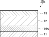
- FIG. 1 shows a schematic cross-sectional view of an embodiment of the photoelectric conversion element of the present invention.
- the photoelectric conversion element 10a shown in FIG. 1 includes a conductive film (hereinafter, also referred to as a lower electrode) 11 that functions as a lower electrode, an electron blocking film 16A, a photoelectric conversion film 12 containing a specific compound described later, and an upper electrode. It has a structure in which a functioning transparent conductive film (hereinafter, also referred to as an upper electrode) 15 is laminated in this order.
- FIG. 2 shows a configuration example of another photoelectric conversion element.
- FIGS. 1 and 2 has a configuration in which an electron blocking film 16A, a photoelectric conversion film 12, a hole blocking film 16B, and an upper electrode 15 are laminated in this order on a lower electrode 11.
- the stacking order of the electron blocking film 16A, the photoelectric conversion film 12, and the hole blocking film 16B in FIGS. 1 and 2 may be appropriately changed depending on the application and characteristics.
- the photoelectric conversion element 10a it is preferable that light is incident on the photoelectric conversion film 12 via the upper electrode 15. Further, when the photoelectric conversion element 10a (or 10b) is used, a voltage can be applied. In this case, it is preferable that the lower electrode 11 and the upper electrode 15 form a pair of electrodes, and a voltage of 1 ⁇ 10 -5 to 1 ⁇ 10 7 V / cm is applied between the pair of electrodes. From the viewpoint of performance and power consumption, the applied voltage is more preferably 1 ⁇ 10 -4 to 1 ⁇ 10 7 V / cm, further preferably 1 ⁇ 10 -3 to 5 ⁇ 10 6 V / cm.
- the voltage application method it is preferable to apply the voltage so that the electron blocking film 16A side becomes the cathode and the photoelectric conversion film 12 side becomes the anode in FIGS. 1 and 2.
- a voltage can be applied by the same method.
- the photoelectric conversion element 10a (or 10b) can be suitably applied to an image sensor application.
- the photoelectric conversion film is a film containing a specific compound.
- the specific compound will be described in detail.
- A is a group represented by any of the formulas (2) to (8). It is also preferable that A is a group represented by any of the formulas (3) to (8).
- R Z represents a hydrogen atom or a halogen atom, and a hydrogen atom is preferable.
- n4 represents 1 or 2.
- R represents a hydrogen atom or a substituent (halogen atom, etc.).
- Y 41 and Y 44 are the same and Y 42 and Y 43 are the same, and / or Y 41 and Y 43 are the same and Y 42.
- Y 44 are preferably the same.
- Y 43 in the Y 42 and the right-hand aromatic ring on the left side of the aromatic ring are the same, and Y 42 in the Y 43 and the right-hand aromatic ring on the left side of the aromatic ring are the same, and, Y 44 in the left side of the aromatic ring and the right It is preferable that it can be said to be the same as Y 41 in the aromatic ring.
- n5 represents 1 or 2.
- R represents a hydrogen atom or a substituent (halogen atom, etc.).
- X 51 represents a sulfur atom, an oxygen atom, or a selenium atom.
- n5 it is preferable that Y 51 and Y 52 are the same.
- the aromatic ring containing the two existing Y 51 , Y 52 , and X 51 has a symmetrical structure.
- the Y 51 in the aromatic ring on the left side and the Y 52 in the aromatic ring on the right side are the same, and the Y 52 in the aromatic ring on the left side.
- identical and Y 51 in the right-hand aromatic ring and the X 51 in X 51 and the right aromatic ring on the left side of the aromatic ring it is preferred that said the same.
- R represents a hydrogen atom or a substituent (halogen atom, etc.).
- ⁇ CF a substituent
- R represents a hydrogen atom or a substituent (halogen atom, etc.).
- A, B and C each independently represent a 5- or 6-ring aromatic ring group.
- the 5-ring or 6-ring aromatic ring group include a furan ring group, a pyrrole ring group, a thiophene ring group, an imidazole ring group, a pyrazole ring group, an oxazole ring group, an isoxazole ring group, a thiazole ring group and an isothiazole.
- aromatic ring groups such as ring groups; 6 ring aromatic ring groups such as benzene ring group, pyridine ring group, pyrazine ring group, pyrimidine ring group, pyridazine ring group and triazine ring group can be mentioned.
- aromatic ring group include a thiazole ring group, an isothiazole ring group, and the like.
- a benzene ring group, a pyridine ring group or a pyridine ring group is preferable.
- A, B and C are condensed with each other to form a fused ring.
- A, B and C are condensed with each other to form a fused ring, that is, the aromatic ring group of 5 or 6 rings represented by A and the aromatic of 5 or 6 rings represented by B. It means that the ring group and the aromatic ring group of 5 or 6 rings represented by C are condensed to form a fused ring.
- A, B and C each represent a benzene ring group
- the condensed ring formed by condensing A, B and C is an anthracene ring group.
- R represents a hydrogen atom or a substituent (halogen atom, etc.).
- ⁇ N is preferable.
- Ar 1 represents an aromatic ring group.
- the aromatic ring group represented by Ar 1 may have a group selected from the group consisting of a halogen atom and an alkyl group having 1 to 2 carbon atoms which may have a halogen atom as a substituent. good.
- the number thereof is, for example, 1 to 4. It is also preferable that the aromatic ring group represented by Ar 1 does not have a substituent.
- Ar 2 represents an aromatic ring group.
- Aromatic ring group represented by Ar 2 as a substituent other than U 1, a halogen atom, and a group selected from the group consisting of an alkyl group having 1 or 2 carbon atoms which may have a halogen atom You may have.
- the above-mentioned substituent (substituent other than U 1 ) that can be possessed by the aromatic ring group represented by Ar 2 is preferably an alkyl group having 1 to 2 carbon atoms which may have a halogen atom.
- the number thereof is, for example, 1 to 4. It is also preferable that the aromatic ring group represented by Ar 2 does not have the above-mentioned substituent.
- U 1 represents a halogen atom, a cyano group, or an aromatic ring group.
- the aromatic ring group represented by U 1 has a halogen atom, an alkyl group having 1 to 2 carbon atoms which may have a halogen atom, and a group selected from the group consisting of a cyano group as a substituent. May be.
- the number thereof is, for example, 1 to 5.
- the aromatic ring group represented by U 1 is, for example, an unsubstituted aromatic ring group, an aromatic ring group having a halogen atom, an aromatic ring group having cyano, and 1 to 2 carbon atoms which may have a halogen atom.
- An aromatic ring group having an alkyl group of is mentioned.
- the aromatic ring group having a halogen atom when the aromatic ring group has a plurality of substituents, at least one (preferably all) of the plurality of substituents may be a halogen atom (fluorine atom or the like).
- aromatic ring group having cyano and the aromatic ring group having an alkyl group having 1 to 2 carbon atoms which may have a halogen atom.
- aromatic ring group represented by U 1 include a phenyl group, a fluorophenyl group (4-fluorophenyl group, etc.), a difluorophenyl group (3,5-difluorophenyl group, etc.), and a trifluorophenyl group (3).
- tetrafluorophenyl group pentafluorophenyl group, (trifluoromethyl) phenyl group (4- (trifluoromethyl) phenyl group, etc.), cyanophenyl group (4-cyanophenyl group, etc.) Etc.), and a nitrogen-containing aromatic ring group.
- m represents an integer of 0 to 2.
- n1 represents an integer of 0 to 5, and an integer of 1 to 5 is preferable. If n1 is 0, U 1 to a 0 n1 is attached does not exist. For example, when n1 on the left side in the equation (1) is 0, U 1 on the left side does not exist, and Ar 1 on the left side does not bind to U 1.
- a X is a group represented by the aforementioned formula (2) or Formula (3).
- U 2 represents a hydrogen atom, a halogen atom, a cyano group, or an aromatic ring group.
- the aromatic ring group represented by U 2 has a halogen atom, an alkyl group having 1 to 2 carbon atoms which may have a halogen atom, and a group selected from the group consisting of a cyano group as a substituent. May be.
- the number thereof is, for example, 1 to 4.
- U 2 is preferably a hydrogen atom or an aromatic ring group.
- R Z represents a hydrogen atom or a halogen atom, and a hydrogen atom is preferable.
- X represents a sulfur atom, an oxygen atom, or a selenium atom.
- m represents an integer of 0 to 2.
- a X is a group represented by the aforementioned formula (2) or Formula (3).
- U 3 represents a halogen atom, a cyano group, or an aromatic ring group.
- the aromatic ring group represented by U 3 has, as a substituent, a group selected from the group consisting of a halogen atom, an alkyl group having 1 to 2 carbon atoms which may have a halogen atom, and a cyano group. May be.
- the aromatic ring group represented by U 3 has a substituent, the number thereof is, for example, 1 to 5.
- the group mentioned as an example of the aromatic ring group represented by U 1 of the formula (1) can be similarly mentioned.
- X represents a sulfur atom, an oxygen atom, or a selenium atom.
- n2 represents 0 or 1. If n2 is 0, U 3 which is 0 n2 is attached does not exist. For example, if n2 on the left side in the formula (1-3) is 0, the left side of the U 3 are not present.
- Equation (2-2) The specific compound is also preferably a compound represented by the formula (2-2).
- the compound represented by the formula (2-2) can be said to be one of the preferred forms of the compound represented by the formula (1-2).
- R Z represents a hydrogen atom or a halogen atom, and a hydrogen atom is preferable.
- X represents a sulfur atom, an oxygen atom, or a selenium atom.
- U 4 is a fluorine atom, a group represented by the formula (4-1), or a group represented by the formula (4-2).
- Equation (4-1) * represents the bond position.
- p1 represents an integer of 1 to 5.
- T 1 represents a cyano group.
- the bonding position of the cyano group may be any of the ortho-position, the meta-position, and the para-position.
- T 1 represents a halogen atom.
- p1 is preferably 2 to 4, more preferably 3 to 4, and even more preferably 3.
- Specific examples of the group represented by the formula (4-1) include a difluorophenyl group (3,5-difluorophenyl group, etc.), a trifluorophenyl group (3,4,5-trifluorophenyl group, etc.), and a tetra. Examples thereof include a fluorophenyl group, a pentafluorophenyl group, and a cyanophenyl group (4-cyanophenyl group, etc.).
- Equation (4-2) * represents the bond position.
- Z represents a nitrogen-containing aromatic ring group.
- p2 represents an integer of 0 to 4. If p2 is 0, T 2 does not exist.
- T 2 represents a halogen atom or a cyano group.
- the U 4 is preferably a group represented by the formula (4-1) having T 1 which is a cyano group, or a group represented by the formula (4-2).
- R Z represents a hydrogen atom or a halogen atom, and a hydrogen atom is preferable.
- X represents a sulfur atom, an oxygen atom, or a selenium atom.
- U 5 is a fluorine atom, a cyano group, a group represented by the formula (4-3), or a group represented by the formula (4-4).
- T 3 represents a halogen atom or a cyano group.
- Examples of the group represented by the formula (4-3) include a group represented by the formula (4-3) having a fluorine atom T 3 and a group having a cyano group T 3 (4-3). The group represented by is mentioned.
- the group represented by the formula (4-3) with a T 3 is a fluorine atom, if T 3 there are a plurality, at least one of T 3 presence of a plurality of (preferably all) may be a fluorine atom ..
- the group represented by the formula (4-3) having T 3 which is a cyano group includes a fluorophenyl group (4-fluorophenyl group, etc.), a difluorophenyl group (3,5-difluorophenyl group, etc.), and a trifluorophenyl group (3,). 4,5-Difluorophenyl group, etc.), tetrafluorophenyl group, pentafluorophenyl group, and cyanophenyl group (4-cyanophenyl group, etc.).
- Equation (4-4) * represents the bond position.
- Z represents a nitrogen-containing aromatic ring group.
- p4 represents an integer from 0 to 4. If p4 is 0, T 4 does not exist.
- T 4 represents a halogen atom, an alkyl group having 1 to 2 carbon atoms which may have a halogen atom, or a cyano group.
- U 5 is preferably a group represented by the formula (4-3) or a group represented by the formula (4-4), and is represented by the formula (4-4). Preferably better than the group.
- R Z represents a hydrogen atom or a halogen atom, and a hydrogen atom is preferable.
- X represents a sulfur atom, an oxygen atom, or a selenium atom.
- U 6 is a fluorine atom, a cyano group, a group represented by the formula (4-5), or a group represented by the formula (4-6).
- T 5 represents a halogen atom, an alkyl group having 1 to 2 carbon atoms which may have a halogen atom, or a cyano group.
- Examples of the group represented by the formula (4-5) include a group represented by the formula (4-5) having a fluorine atom T 5 and a group having a cyano group T 5 (4-5).
- a group represented by, and include a group represented by the formula (4-5) with a T 5 is also an alkyl group having 1 or 2 carbon atoms and a halogen atom.
- T 5 is a fluorine atom
- at least one T 5 presence of a plurality of (preferably all) may be a fluorine atom .
- Specific examples of the group represented by the formula (4-5) include a phenyl group, a fluorophenyl group (4-fluorophenyl group, etc.), a difluorophenyl group (3,5-difluorophenyl group, etc.), and a trifluorophenyl group. (3,4,5-difluorophenyl group, etc.), tetrafluorophenyl group, pentafluorophenyl group, trifluoromethylphenyl group (4- (trifluoromethyl) phenyl group, etc.), and cyanophenyl group (4-cyano). Phenyl group, etc.).
- Equation (4-6) * represents the bond position.
- Z represents a nitrogen-containing aromatic ring group.
- p4 represents an integer from 0 to 4. If p4 is 0, T 6 is not present.
- T 6 represents a halogen atom, an alkyl group having 1 to 2 carbon atoms which may have a halogen atom, or a cyano group.
- U 6 is cyano group
- a group represented by the formula with a T 5 is a fluorine atom (4-5)
- the formula (4-5) with a T 5 is cyano group
- a group represented by the formula (4-6) or a group represented by the formula (4-6) is preferable, a group represented by the formula (4-5) having a T 5 which is a fluorine atom, and a formula having a T 5 which is a cyano group.
- the group represented by (4-5) or the group represented by the formula (4-6) is more preferable, and the group represented by the formula (4-5) having T 5 which is a cyano group or the group is represented by the formula (4-5).
- the group represented by the formula (4-6) is more preferable.
- R Z represents a hydrogen atom or a halogen atom, and a hydrogen atom is preferable.
- X represents a sulfur atom, an oxygen atom, or a selenium atom.
- E represents an aromatic ring.
- the aromatic ring represented by E is condensed with a five-membered ring bonded with one R Z, share the five-membered ring and 2 carbon atoms as ring members atoms.
- the aromatic ring represented by E is, as substituents other than U 6, may have a halogen atom.
- the substituents aromatic ring may have represented by E (substituents are other than U 6) is a halogen atom other than a fluorine atom is preferred.
- the aromatic ring represented by E has the above-mentioned substituent, the number thereof is, for example, 1 to 3. It is also preferable that the aromatic ring represented by E does not have the substituent.
- n3 represents an integer of 0 to 4. If n3 is 0, U 6 which is 0 n3 is attached does not exist. For example, if n3 on the left side in equation (3-4) is 0, U 6 on the left side does not exist and E on the left side does not combine with U 6.
- U 6 is a fluorine atom, a cyano group, a group represented by the formula (4-5), or a group represented by the formula (4-6). Equations (4-5) and (4-6) are as described above.
- R Z represents a hydrogen atom or a halogen atom, and a hydrogen atom is preferable.
- U 6 is a fluorine atom, a cyano group, a group represented by the formula (4-5), or a group represented by the formula (4-6). Equations (4-5) and (4-6) are as described above.
- R Z represents a hydrogen atom or a halogen atom, and a hydrogen atom is preferable.
- U 6 is a fluorine atom, a cyano group, a group represented by the formula (4-5), or a group represented by the formula (4-6). Equations (4-5) and (4-6) are as described above.
- U 6 is represented by a group represented by the formula (4-5) having a fluorine atom T 5 and a formula (4-5) having a cyano group T 5.
- a group or a group represented by the formula (4-6) is preferable, and a group represented by the formula (4-6) is more preferable.
- AY is a group represented by any of the above formulas (2) to (8).
- U 2 represents a hydrogen atom, a halogen atom, a cyano group, or an aromatic ring group.
- the aromatic ring group represented by U 2 has a halogen atom, an alkyl group having 1 to 2 carbon atoms which may have a halogen atom, and a group selected from the group consisting of a cyano group as a substituent. May be.
- the aromatic ring group represented by U 2 has a substituent, the number thereof is, for example, 1 to 4.
- R Z represents a hydrogen atom or a halogen atom, and a hydrogen atom is preferable.
- R represents a hydrogen atom or a substituent (halogen atom or the like).
- AY is a group represented by any of the above formulas (2) to (8).
- U 2 represents a hydrogen atom, a halogen atom, a cyano group, or an aromatic ring group.
- the aromatic ring group represented by U 2 has a halogen atom, an alkyl group having 1 to 2 carbon atoms which may have a halogen atom, and a group selected from the group consisting of a cyano group as a substituent. May be.
- the aromatic ring group represented by U 2 has a substituent, the number thereof is, for example, 1 to 4.
- R Z represents a hydrogen atom or a halogen atom, and a hydrogen atom is preferable.
- X represents a sulfur atom, an oxygen atom, or a selenium atom.
- AY is a group represented by any of the above formulas (2) to (8).
- U 2 represents a hydrogen atom, a halogen atom, a cyano group, or an aromatic ring group.
- the aromatic ring group represented by U 2 has a halogen atom, an alkyl group having 1 to 2 carbon atoms which may have a halogen atom, and a group selected from the group consisting of a cyano group as a substituent. May be.
- the aromatic ring group represented by U 2 has a substituent, the number thereof is, for example, 1 to 4.
- R Z represents a hydrogen atom or a halogen atom, and a hydrogen atom is preferable.
- R represents a hydrogen atom or a substituent (halogen atom or the like).
- AY is a group represented by any of the above formulas (2) to (8).
- U 2 represents a hydrogen atom, a halogen atom, a cyano group, or an aromatic ring group.
- the aromatic ring group represented by U 2 has a halogen atom, an alkyl group having 1 to 2 carbon atoms which may have a halogen atom, and a group selected from the group consisting of a cyano group as a substituent. May be.
- the aromatic ring group represented by U 2 has a substituent, the number thereof is, for example, 1 to 4.
- R Z represents a hydrogen atom or a halogen atom, and a hydrogen atom is preferable.
- X represents a sulfur atom, an oxygen atom, or a selenium atom.
- the specific compound has a symmetrical structure. It is also preferable that the specific compound has, for example, two groups represented by "-(Ar 1 ) m- Ar 2- (U 1 ) n1" existing in the formula (1) having the same structure.
- the molecular weight of the specific compound is not particularly limited, and is preferably 400 to 1200, more preferably 400 to 900. When the molecular weight is 1200 or less, the vapor deposition temperature does not rise and the decomposition of the compound is unlikely to occur. When the molecular weight is 400 or more, the glass transition point of the vapor-deposited film is not lowered, and the heat resistance of the photoelectric conversion element is improved.
- the specific compound is particularly useful as a material for a photoelectric conversion film used in an image sensor, an optical sensor, or a photovoltaic cell.
- the specific compound can also be used as a coloring material, a liquid crystal material, an organic semiconductor material, a charge transport material, a pharmaceutical material, and a fluorescent diagnostic agent material.
- the specific compound is preferably a compound having an ionization potential of -5.0 to -6.0 eV in a single film in terms of matching the energy level with the n-type semiconductor material described later.
- the maximum absorption wavelength of the specific compound is not particularly limited, and is preferably in the range of, for example, 350 to 550 nm, and more preferably in the range of 400 to 550 nm.
- the maximum absorption wavelength is a value measured in a solution state (solvent: chloroform) by adjusting the absorption spectrum of the specific compound to a concentration such that the absorbance becomes 0.5 to 1.
- solvent chloroform
- the specific compound is not soluble in chloroform, the value measured using the specific compound in a film state after vapor deposition of the specific compound is used as the maximum absorption wavelength of the specific compound.
- the maximum absorption wavelength of the photoelectric conversion film is not particularly limited, and is preferably in the range of, for example, 300 to 700 nm, and more preferably in the range of 400 to 700 nm.
- the specific compound may be used alone or in combination of two or more.
- the photoelectric conversion film contains a dye as a component other than the above-mentioned specific compound.
- the dye is preferably an organic dye.
- the above-mentioned pigments include, for example, cyanine pigments, styryl pigments, hemicyanine pigments, merocyanine pigments (including zero methine merocyanin (simple merocyanin)), rodacyanine pigments, allopolar pigments, oxonols pigments, hemioxonor pigments, squalium pigments, croconium pigments, and azamethines.
- the content of the dye with respect to the total content of the specific compound and the dye in the photoelectric conversion film (film thickness in terms of single layer of dye / (film thickness in terms of single layer of specific compound + single dye)
- the film thickness) ⁇ 100)) in terms of layers is preferably 15 to 75% by volume, more preferably 20 to 60% by volume, and even more preferably 25 to 50% by volume.
- the dye may be used alone or in combination of two or more.
- the photoelectric conversion film further contains an n-type semiconductor material as a component other than the above-mentioned specific compound and dye.
- the n-type semiconductor material is an acceptor-type organic semiconductor material (compound), and refers to an organic compound having a property of easily accepting electrons. More specifically, the n-type semiconductor material is preferably an organic compound having a higher electron affinity than the specific compound when used in contact with the above-mentioned specific compound.
- the n-type semiconductor material is preferably an organic compound having a higher electron affinity than the dye when used in contact with the above-mentioned dye.
- the electron affinity of the n-type semiconductor material is preferably 3.0 to 5.0 eV.
- the n-type semiconductor material includes, for example, fullerene selected from the group consisting of fullerene and its derivatives, condensed aromatic carbocyclic compounds (for example, naphthalene derivatives, anthracene derivatives, phenanthrene derivatives, tetracene derivatives, pyrene derivatives, perylene derivatives, and , Fluolanthene derivative); 5- to 7-membered heterocyclic compounds having at least one nitrogen atom, oxygen atom, and sulfur atom (eg, pyridine, pyrazine, pyrimidine, pyridazine, triazine, quinoline, quinoxalin, quinazoline, phthalazine).
- fullerene selected from the group consisting of fullerene and its derivatives, condensed aromatic carbocyclic compounds (for example, naphthalene derivatives, anthracene derivatives, phenanthrene derivatives, tetracene derivatives, pyrene
- Examples thereof include styrylallylene derivatives; metal complexes having a nitrogen-containing heterocyclic compound as a ligand; silol compounds; and the compounds described in paragraphs [0056] to [0057] of JP-A-2006-1000377.
- the n-type semiconductor material preferably contains fullerenes selected from the group consisting of fullerenes and derivatives thereof.
- fullerenes selected from the group consisting of fullerenes and derivatives thereof.
- the fullerene include fullerene C60, fullerene C70, fullerene C76, fullerene C78, fullerene C80, fullerene C82, fullerene C84, fullerene C90, fullerene C96, fullerene C240, fullerene C540, and mixed fullerene.
- the fullerene derivative include compounds in which a substituent is added to the above fullerene.
- the substituent is preferably an alkyl group, an aryl group, or a heterocyclic group.
- the fullerene derivative the compound described in JP-A-2007-123707 is preferable.
- the thickness / thickness of a specific compound in terms of a single layer + film thickness of a dye in terms of a single layer + film thickness of an n-type semiconductor material in terms of a single layer) ⁇ 100)
- the n-type semiconductor material may be used alone or in combination of two or more.
- the total thickness of the semiconductor materials) ⁇ 100) is preferably 50 to 100% by volume, more preferably 80 to 100% by volume.
- the fullerenes may be used alone or in combination of two or more.
- the molecular weight of the n-type semiconductor material is preferably 200 to 1200, more preferably 200 to 1000.
- the photoelectric conversion film is substantially composed of only a specific compound, a dye, and an n-type semiconductor material.
- the fact that the photoelectric conversion film is substantially composed of only the specific compound, the dye, and the n-type semiconductor material means that the total content of the specific compound, the dye, and the n-type semiconductor material is 95 with respect to the total mass of the photoelectric conversion film. It means that it is ⁇ 100% by mass.
- the photoelectric conversion film is preferably a mixed layer formed in a state where a specific compound and a dye are mixed.
- the photoelectric conversion film contains an n-type semiconductor material
- the photoelectric conversion film is preferably a mixed layer formed by mixing a specific compound and the n-type semiconductor material.
- the photoelectric conversion film contains a dye and an n-type semiconductor material
- the photoelectric conversion film is preferably a mixed layer formed by mixing a specific compound, a dye, and an n-type semiconductor material.
- a mixed layer is a layer in which two or more kinds of materials are mixed in a single layer.
- the photoelectric conversion film containing a specific compound is a non-luminescent film, and has characteristics different from those of an organic electroluminescent device (OLED: Organic Light Emitting Diode).
- the non-emission film is intended to be a film having an emission quantum efficiency of 1% or less, and the emission quantum efficiency is preferably 0.5% or less, more preferably 0.1% or less.
- the photoelectric conversion film can be formed mainly by a dry film forming method.
- the dry film forming method includes, for example, a vapor deposition method (particularly, a vacuum vapor deposition method), a sputtering method, an ion plating method, a physical vapor deposition method such as an MBE (Molecular Beam Epitaxy) method, and a CVD method such as plasma polymerization. (Chemical Vapor Deposition) method can be mentioned. Of these, the vacuum vapor deposition method is preferable.
- the manufacturing conditions such as the degree of vacuum and the vapor deposition temperature can be set according to a conventional method.
- the thickness of the photoelectric conversion film is preferably 10 to 1000 nm, more preferably 50 to 800 nm, further preferably 50 to 500 nm, and particularly preferably 50 to 400 nm.
- the electrodes are made of a conductive material.
- the conductive material include metals, alloys, metal oxides, electrically conductive compounds, and mixtures thereof. Since light is incident from the upper electrode 15, it is preferable that the upper electrode 15 is transparent to the light to be detected.
- the material constituting the upper electrode 15 is, for example, antimony or fluorine-doped tin oxide (ATO: Antimony Tin Oxide, FTO: Fluorine topped Tin Oxide), tin oxide, zinc oxide, indium oxide, indium tin oxide (ITO: Conductive metal oxides such as Indium Tin Oxide) and indium tin oxide (IZO); metal thin films such as gold, silver, chromium, and nickel; these metals and conductive metal oxides. Examples thereof include mixtures or laminates; organic conductive materials such as polyaniline, polythiophene and polypyrrole; and carbon materials such as graphene and carbon nanotubes. Of these, conductive metal oxides are preferable from the viewpoint of high conductivity and transparency.
- the sheet resistance may be, for example, 100 to 10000 ⁇ / ⁇ .
- the degree of freedom in the range of film thickness that can be thinned is large.
- Increasing the light transmittance is preferable because it increases the light absorption in the photoelectric conversion film and increases the photoelectric conversion ability.
- the film thickness of the upper electrode 15 is preferably 5 to 100 nm, more preferably 5 to 20 nm.
- the lower electrode 11 may be transparent or may reflect light without being transparent, depending on the intended use.
- the material constituting the lower electrode 11 is, for example, antimony or fluorine-doped tin oxide (ATO, FTO), tin oxide, zinc oxide, indium oxide, indium tin oxide (ITO), and indium tin oxide (IZO).
- Conductive metal oxides such as; metals such as gold, silver, chromium, nickel, titanium, tungsten, and aluminum, and conductive compounds such as oxides or nitrides of these metals (eg, titanium nitride (TiN)). ); Mixtures or laminates of these metals and conductive metal oxides; Organic conductive materials such as polyaniline, polythiophene, and polypyrrole; and carbon materials such as graphene and carbon nanotubes, etc. Can be mentioned.
- the method for forming the electrode is not particularly limited and can be appropriately selected depending on the electrode material. Specifically, a wet method such as a printing method and a coating method; a physical method such as a vacuum vapor deposition method, a sputtering method, and an ion plating method; and a chemical method such as CVD and plasma CVD method. , Etc. can be mentioned.
- the electrode material is ITO, examples thereof include an electron beam method, a sputtering method, a resistance heating vapor deposition method, a chemical reaction method (sol-gel method, etc.), and a method of applying a dispersion of indium tin oxide.
- the photoelectric conversion element of the present invention has one or more intermediate layers in addition to the photoelectric conversion film between the conductive film and the transparent conductive film.
- the intermediate layer include a charge blocking film.
- the charge blocking film include an electron blocking film and a hole blocking film.
- the electron blocking film is a donor organic semiconductor material (compound), and for example, the following p-type organic semiconductor can be used.
- One type of p-type organic semiconductor may be used alone, or two or more types may be used.
- the p-type organic semiconductor is, for example, a triarylamine compound (for example, N, N'-bis (3-methylphenyl)-(1,1'-biphenyl) -4,4'-diamine (TPD), 4,4.
- TPD triarylamine
- '-Bis [N- (naphthyl) -N-phenyl-amino] biphenyl ( ⁇ -NPD) the compound described in paragraphs [0128] to [0148] of JP2011-228614A, JP-A-2011-176259.
- cyanine compounds oxonol compounds, polyamine compounds, indol compounds, pyrrol compounds, pyrazole compounds, polyarylene compounds, condensed aromatic carbocyclic compounds ( example For example, naphthalene derivative, anthracene derivative, phenanthrene derivative, tetracene derivative, pentacene derivative, pyrene derivative, perylene derivative, and fluorantene derivative), porphyrin compound, phthalocyanine compound, triazole compound, oxadiazole compound, imidazole compound, polyarylalkane compound.
- p-type organic semiconductor examples include compounds having a smaller ionization potential than the n-type semiconductor material, and if this condition is satisfied, the dyes as described above can also be used.
- a polymer material can also be used as the electron blocking film.
- the polymer material include polymers such as phenylene vinylene, fluorene, carbazole, indole, pyrrole, pyrrole, picolin, thiophene, acetylene, and diacetylene, and derivatives thereof.
- the electron blocking film may be composed of a plurality of films.
- the electron blocking film may be made of an inorganic material.
- Inorganic materials that can be electron blocking films include, for example, calcium oxide, chromium oxide, copper oxide, manganese oxide, cobalt oxide, nickel oxide, copper oxide, gallium copper oxide, strontium oxide copper, niobium oxide, molybdenum oxide, and indium copper oxide. , Indium silver oxide, and iridium oxide.
- the hole blocking film is an acceptor-type organic semiconductor material (compound), and the above-mentioned n-type semiconductor material or the like can be used.
- the method for producing the charge blocking film is not particularly limited, and examples thereof include a dry film forming method and a wet film forming method.
- the dry film forming method include a vapor deposition method and a sputtering method.
- the vapor deposition method may be any of a physical vapor deposition (PVD) method and a chemical vapor deposition (CVD) method, and a physical vapor deposition method such as a vacuum vapor deposition method is preferable.
- Examples of the wet film forming method include an inkjet method, a spray method, a nozzle printing method, a spin coating method, a dip coating method, a casting method, a die coating method, a roll coating method, a bar coating method, and a gravure coating method.
- the inkjet method is preferable from the viewpoint of precision patterning.
- the thickness of the charge blocking film is preferably 3 to 200 nm, more preferably 5 to 100 nm, and even more preferably 5 to 30 nm, respectively.
- the photoelectric conversion element may further have a substrate.
- the type of substrate used is not particularly limited, and examples thereof include a semiconductor substrate, a glass substrate, and a plastic substrate.
- the position of the substrate is not particularly limited, and usually, a conductive film, a photoelectric conversion film, and a transparent conductive film are laminated on the substrate in this order.
- the photoelectric conversion element may further have a sealing layer.
- the performance of the photoelectric conversion material may be significantly deteriorated due to the presence of deterioration factors such as water molecules. Therefore, the entire photoelectric conversion film is coated with a dense metal oxide, metal nitride, ceramics such as metal nitride, or a sealing layer such as diamond-like carbon (DLC: Diamond-like Carbon) that does not allow water molecules to permeate.
- DLC Diamond-like Carbon
- the photoelectric conversion element is an element that converts the optical information of an image into an electric signal. Normally, a plurality of photoelectric conversion elements are arranged in a matrix on the same plane, and each photoelectric conversion element (pixel) has an optical signal. Is converted into an electric signal, and the electric signal can be sequentially output to the outside of the image sensor for each pixel. Therefore, each pixel is composed of one or more photoelectric conversion elements and one or more transistors.
- the image pickup element is mounted on a digital camera, an image pickup element such as a digital video camera, an electronic endoscope, and an image pickup module such as a mobile phone.
- the photoelectric conversion element of the present invention is also preferably used for an optical sensor having the photoelectric conversion element of the present invention.
- the optical sensor may be used by the photoelectric conversion element alone, or may be used as a line sensor in which the photoelectric conversion elements are arranged in a straight line, or a two-dimensional sensor in which the photoelectric conversion elements are arranged in a plane.
- the present invention also relates to compounds.
- the compound of the present invention includes a compound represented by the formula (2-2), a compound represented by the formula (3-2), and a compound represented by the formula (3-3) among the above-mentioned specific compounds.
- the mixed solution was heated and stirred at 100 ° C. for 8 hours. Then, the temperature of the mixed solution was lowered to room temperature (25 ° C.), and the mixture was filtered. The obtained residue (filter) was suspended and washed with chloroform, and then filtered. The obtained residue (filter) was dried under reduced pressure and sublimated and purified to obtain 4.62 g of compound (I-2-5).
- the evaluation dye compound (B-1) is the same compound as the comparative compound (QD).
- N-type semiconductor material Fullerene C60 was used as an n-type semiconductor material used for evaluation in the production of a photoelectric conversion element described later.
- the photoelectric conversion element includes a lower electrode 11, an electron blocking film 16A, a photoelectric conversion film 12, a hole blocking film 16B, and an upper electrode 15.
- amorphous ITO is formed into a film on a glass substrate by a sputtering method to form a lower electrode 11 (thickness: 30 nm), and the following compound (C-1) is further vacuumed on the lower electrode 11.
- a film was formed by a heat vapor deposition method to form an electron blocking film 16A (thickness: 10 nm).
- the evaluation compound one of the above-mentioned evaluation compounds
- the n-type semiconductor material Fralerene C60
- the dye the above-mentioned
- One of the evaluation dyes is set to a vapor deposition rate of 2.0 ⁇ / sec, and the film is co-deposited by the vacuum vapor deposition method so that each has a single layer equivalent of 100 nm, and the total film thickness is 300 nm.
- the photoelectric conversion film 12 as a layer was formed (photoelectric conversion film forming step).
- the photoelectric conversion film 12 which is a mixed layer having a total film thickness of 200 nm was formed without using an n-type semiconductor material. Further, the following compound (C-2) was formed on the photoelectric conversion film 12 to form a hole blocking film 16B (thickness: 10 nm). Further, an amorphous ITO was formed on the hole blocking film 16B by a sputtering method to form an upper electrode 15 (transparent conductive film) (thickness: 10 nm).
- an aluminum oxide (Al 2 O 3 ) layer is formed on the SiO film by an ALCVD (Atomic Layer Chemical Vapor Deposition) method.
- ALCVD Atomic Layer Chemical Vapor Deposition
- a photoelectric conversion element (also simply referred to as “element”) of a comparative example was manufactured.
- 10 elements of the same type prepared by the same procedure were prepared and subjected to the evaluation described later.
- the external quantum efficiency When the external quantum efficiency is 92% or more, it is “A”, when it is 90% or more and less than 92%, it is “B”, when it is 87% or more and less than 90%, it is “C”, and when it is 85% or more and less than 87%, it is “C”.
- the sensitivity was evaluated as “D”, “E” when it was 82% or more and less than 85%, and "F” when it was less than 82%. Practically, the evaluation is preferably “D” or higher, more preferably “C” or higher, and even more preferably "B” or higher.
- the rise time of each of the 10 elements of the same type was measured, and the average rise time was taken as the rise time of the element of that type.
- the relative value of the rise time of each element was obtained when the rise time of the elements of Comparative Example 1 was 1.
- the relative value of the rise time is "AA” when it is less than 0.10, "A” when it is 0.10 or more and less than 0.15, and “B” when it is 0.15 or more and less than 0.20.
- C for 0.20 or more and less than 0.25
- D for 0.25 or more and less than 0.30
- E for 0.30 or more and less than 1.00, 1.00 or more.
- the case was designated as "F” and the responsiveness was evaluated. Practically, it is preferably “D” or more, more preferably “C” or more, and even more preferably "B” or more.
- the standard deviation can be calculated by the following formula. s: standard deviation n: 10 x: 1 x i : Rise time of the i-th element when the average value of the rise time of 10 elements is standardized as 1.
- the relative value is 0.98 or more, it is "A”, if it is 0.95 or more and less than 0.98, it is “B”, if it is 0.93 or more and less than 0.95, it is “C”, and it is 0.90 or more.
- the heat resistance was evaluated as “D” when it was less than 0.93 and as "E” when it was less than 0.90.
- the evaluation compound is a compound that can be represented by a plurality of these formulas, it is shown as being represented by the formulas listed later.
- the compound is a compound that can be represented by any of the formula (1), the formula (1-2), and the formula (3-2), in the “formula” column, the formula (3-2) is used. Shown as the compound represented.
- the "U” column indicates the form of the group represented by any of U 1 to U 6 possessed by the specific compound used.
- the "aromatic ring group” is in the formula (1-2), the formula (1-4), the formula (1-5), the formula (1-6), the formula (1-7), and the formula (1-8).
- U 2 or U 3 in the formula (1-3) is an aromatic ring group (this aromatic ring group has a halogen atom as a substituent, an alkyl group having 1 to 2 carbon atoms which may have a halogen atom, and an alkyl group having 1 to 2 carbon atoms. , May have a group selected from the group consisting of cyano groups), where "4-1F” is represented by the formula (4-1) having T 1 which is a fluorine atom. It means a group, "4-1CN” means a group represented by the formula (4-1) having T 1 which is a cyano group, and "4-2" is represented by the formula (4-2).
- the "dye” and “n-type semiconductor material” columns indicate the type of dye or n-type semiconductor material used in the fabrication of the device, respectively.
- the heat resistance test was carried out only in some examples or comparative examples, and in the examples in which the heat resistance test was not carried out, the heat resistance evaluation column was left blank.
- the specific compound is a formula (1-2), a formula (1-3), a formula (2-2), a formula (3-2), a formula (3-3), a formula (3-4), a formula ( 3-5), Eq. (3-6), Eq. (1-4), Eq. (1-5), Eq. (1-6), Eq. (1-7), or Eq. (1-8) It was confirmed that the effect of the present invention is more excellent in the case of the compound to be used.
- the specific compound is the formula (2-2), the formula (3-2), the formula (3-3), the formula (3-4), the formula (3-5), the formula (3-6), the formula (1-). 4), the compound represented by the formula (1-5), the formula (1-6), the formula (1-7), or the formula (1-8), the effect of the present invention may be further excellent. confirmed.
- the group represented by U 2 is preferably a hydrogen atom or an aromatic ring group from the viewpoint that the effect of the present invention is more excellent. .. Further, it was confirmed that a hydrogen atom is preferable for R z (see comparison of results of Examples 36 to 41, 44 to 50, 138 to 145, etc.).
- the group represented by U 4 is represented by the formula (4-1) having T 1 which is a cyano group, because the effect of the present invention is more excellent. It was confirmed that the group or the group represented by the formula (4-2) is preferable (see comparison of the results of Examples 1 to 35 and the like).
- the group represented by U 5 is a group represented by the formula (4-3), or Formula (4 It was confirmed that the group represented by 4) is preferable and the group represented by the formula (4-4) is preferable (see comparison of the results of Examples 1 to 35 and the like).
- the group represented by U 6 is represented by the formula (4-5) having a cyano group and T 5 which is a fluorine atom.
- a group represented by a group, a group represented by the formula (4-5) having a T 5 which is a cyano group, or a group represented by the formula (4-6) is preferable, and a formula having a T 5 which is a fluorine atom is preferable.
- a group represented by (4-5), a group represented by the formula (4-5) having T 5 which is a cyano group, or a group represented by the formula (4-6) is more preferable. It was confirmed that the group represented by the formula (4-5) or the group represented by the formula (4-6) having T 5 is more preferable (comparison of the results of Examples 74 to 110, etc.). See).
- the group represented by U 5 is represented by the formula (4-5) having T 5 which is a fluorine atom because the effect of the present invention is more excellent.
- a group represented by the formula (4-5) having a T 5 which is a cyano group or a group represented by the formula (4-6) is preferable, and a group represented by the formula (4-6) is preferable. It was confirmed that it was more preferable (see comparison of results of Examples 119 to 137, etc.).
- the specific compound is represented by the formula (2-2), the formula (3-2), the formula (3-3), the formula (3-6), and the formula (1-4).
- the compound represented by the formula (1-5), the formula (1-6), the formula (1-7), or the formula (1-8) is preferable, and the formula (3-2), the formula (3-2). 3-3), formula (3-6), formula (1-4), formula (1-5), formula (1-6), formula (1-7), or formula (1-8). It is more preferable that the compound is represented by the formula (1-4), the formula (1-5), the formula (1-6), the formula (1-7), or the formula (1-8). It was confirmed that the compound is more preferable.
Landscapes
- Chemical & Material Sciences (AREA)
- Engineering & Computer Science (AREA)
- Materials Engineering (AREA)
- Organic Chemistry (AREA)
- Physics & Mathematics (AREA)
- Spectroscopy & Molecular Physics (AREA)
- Nanotechnology (AREA)
- Heterocyclic Carbon Compounds Containing A Hetero Ring Having Oxygen Or Sulfur (AREA)
- Nitrogen And Oxygen Or Sulfur-Condensed Heterocyclic Ring Systems (AREA)
- Light Receiving Elements (AREA)
- Plural Heterocyclic Compounds (AREA)
- Hybrid Cells (AREA)
Priority Applications (3)
| Application Number | Priority Date | Filing Date | Title |
|---|---|---|---|
| CN202180038051.1A CN115700059A (zh) | 2020-05-29 | 2021-05-28 | 光电转换元件、摄像元件、光传感器及化合物 |
| JP2022526674A JP7545472B2 (ja) | 2020-05-29 | 2021-05-28 | 光電変換素子、撮像素子、光センサ、化合物 |
| US18/059,397 US20230132579A1 (en) | 2020-05-29 | 2022-11-28 | Photoelectric conversion element, imaging element, optical sensor, and compound |
Applications Claiming Priority (6)
| Application Number | Priority Date | Filing Date | Title |
|---|---|---|---|
| JP2020094717 | 2020-05-29 | ||
| JP2020-094717 | 2020-05-29 | ||
| JP2020-129186 | 2020-07-30 | ||
| JP2020129186 | 2020-07-30 | ||
| JP2021088324 | 2021-05-26 | ||
| JP2021-088324 | 2021-05-26 |
Related Child Applications (1)
| Application Number | Title | Priority Date | Filing Date |
|---|---|---|---|
| US18/059,397 Continuation US20230132579A1 (en) | 2020-05-29 | 2022-11-28 | Photoelectric conversion element, imaging element, optical sensor, and compound |
Publications (1)
| Publication Number | Publication Date |
|---|---|
| WO2021241741A1 true WO2021241741A1 (ja) | 2021-12-02 |
Family
ID=78744640
Family Applications (1)
| Application Number | Title | Priority Date | Filing Date |
|---|---|---|---|
| PCT/JP2021/020462 Ceased WO2021241741A1 (ja) | 2020-05-29 | 2021-05-28 | 光電変換素子、撮像素子、光センサ、化合物 |
Country Status (4)
| Country | Link |
|---|---|
| US (1) | US20230132579A1 (https=) |
| JP (1) | JP7545472B2 (https=) |
| CN (1) | CN115700059A (https=) |
| WO (1) | WO2021241741A1 (https=) |
Cited By (1)
| Publication number | Priority date | Publication date | Assignee | Title |
|---|---|---|---|---|
| WO2024128163A1 (en) * | 2022-12-16 | 2024-06-20 | Koala Tech Inc. | Organic solid-state laser, compound and use thereof |
Citations (4)
| Publication number | Priority date | Publication date | Assignee | Title |
|---|---|---|---|---|
| WO2007125692A1 (ja) * | 2006-04-27 | 2007-11-08 | Toyo Ink Mfg. Co., Ltd. | 有機エレクトロルミネッセンス素子用材料ならびに有機エレクトロルミネッセンス素子 |
| KR20140104842A (ko) * | 2013-02-21 | 2014-08-29 | 서울대학교산학협력단 | 벤조싸이아다이아졸 유도체 화합물, 이의 제조방법 및 이를 이용한 유기 태양전지 |
| WO2018016570A1 (ja) * | 2016-07-20 | 2018-01-25 | ソニー株式会社 | 固体撮像素子および固体撮像装置 |
| CN110862388A (zh) * | 2019-11-27 | 2020-03-06 | 中国科学院苏州纳米技术与纳米仿生研究所南昌研究院 | 有机太阳能电池用小分子电子受体材料、其制法及应用 |
Family Cites Families (2)
| Publication number | Priority date | Publication date | Assignee | Title |
|---|---|---|---|---|
| JP2011165747A (ja) | 2010-02-05 | 2011-08-25 | Yamamoto Chem Inc | 有機トランジスタ |
| CN103936653A (zh) | 2013-12-12 | 2014-07-23 | 石家庄诚志永华显示材料有限公司 | 苯并咔唑类oled材料及其制备方法与应用 |
-
2021
- 2021-05-28 JP JP2022526674A patent/JP7545472B2/ja active Active
- 2021-05-28 CN CN202180038051.1A patent/CN115700059A/zh active Pending
- 2021-05-28 WO PCT/JP2021/020462 patent/WO2021241741A1/ja not_active Ceased
-
2022
- 2022-11-28 US US18/059,397 patent/US20230132579A1/en not_active Abandoned
Patent Citations (4)
| Publication number | Priority date | Publication date | Assignee | Title |
|---|---|---|---|---|
| WO2007125692A1 (ja) * | 2006-04-27 | 2007-11-08 | Toyo Ink Mfg. Co., Ltd. | 有機エレクトロルミネッセンス素子用材料ならびに有機エレクトロルミネッセンス素子 |
| KR20140104842A (ko) * | 2013-02-21 | 2014-08-29 | 서울대학교산학협력단 | 벤조싸이아다이아졸 유도체 화합물, 이의 제조방법 및 이를 이용한 유기 태양전지 |
| WO2018016570A1 (ja) * | 2016-07-20 | 2018-01-25 | ソニー株式会社 | 固体撮像素子および固体撮像装置 |
| CN110862388A (zh) * | 2019-11-27 | 2020-03-06 | 中国科学院苏州纳米技术与纳米仿生研究所南昌研究院 | 有机太阳能电池用小分子电子受体材料、其制法及应用 |
Non-Patent Citations (3)
| Title |
|---|
| ANDO, S. ET AL.: "Physical properties and field- effect transistors based on novel thiazolothiazole/heterocyclic and thiazolothiazole/phenylene co-oligomers", SYNTHETIC METALS, vol. 156, 2006, pages 327 - 331, XP025086499, DOI: 10.1016/j.synthmet.2005.12.014 * |
| MOHAJERI AFSHAN, OMIDVAR AKBAR, SETOODEH HENGAMEH: "Fine Structural Tuning of Thieno[3,2- b ] Pyrrole Donor for Designing Banana-Shaped Semiconductors Relevant to Organic Field Effect Transistors", JOURNAL OF CHEMICAL INFORMATION AND MODELING, AMERICAN CHEMICAL SOCIETY , WASHINGTON DC, US, vol. 59, no. 5, 28 May 2019 (2019-05-28), US , pages 1930 - 1945, XP055881051, ISSN: 1549-9596, DOI: 10.1021/acs.jcim.8b00738 * |
| ZHENG HAO, ZHAO YANG, SONG MING-XING, WANG JIN, CHEN LI-QIAO, SUN LEI, BAI FU-QUAN: "Influences of donor/acceptor ratio on the optical and electrical properties of the D/A alternating model oligomers: A density functional theory study", SPECTROCHIMICA ACTA PART A: MOLECULAR AND BIOMOLECULAR SPECTROSCOPY, ELSEVIER, AMSTERDAM, NL, vol. 199, 15 June 2018 (2018-06-15), AMSTERDAM, NL, pages 260 - 270, XP055881059, ISSN: 1386-1425, DOI: 10.1016/j.saa.2018.03.067 * |
Cited By (1)
| Publication number | Priority date | Publication date | Assignee | Title |
|---|---|---|---|---|
| WO2024128163A1 (en) * | 2022-12-16 | 2024-06-20 | Koala Tech Inc. | Organic solid-state laser, compound and use thereof |
Also Published As
| Publication number | Publication date |
|---|---|
| JPWO2021241741A1 (https=) | 2021-12-02 |
| CN115700059A (zh) | 2023-02-03 |
| JP7545472B2 (ja) | 2024-09-04 |
| US20230132579A1 (en) | 2023-05-04 |
Similar Documents
| Publication | Publication Date | Title |
|---|---|---|
| JP7366841B2 (ja) | 光電変換素子、撮像素子、光センサ、化合物 | |
| CN115516655A (zh) | 光电转换元件、摄像元件、光传感器及化合物 | |
| TW201942107A (zh) | 光電轉換元件、攝像元件、光感測器、化合物 | |
| JP7819126B2 (ja) | 光電変換素子、撮像素子、光センサ、化合物 | |
| JP7367050B2 (ja) | 光電変換素子、撮像素子、光センサ、光電変換素子用材料、化合物 | |
| JP7545472B2 (ja) | 光電変換素子、撮像素子、光センサ、化合物 | |
| KR20250168531A (ko) | 광전 변환 소자, 촬상 소자, 광센서, 촬상 소자의 제조 방법, 화합물 | |
| JP7709464B2 (ja) | 光電変換素子、撮像素子、光センサ、化合物 | |
| JP7664280B2 (ja) | 光電変換素子、撮像素子、光センサ、化合物 | |
| JP7445767B2 (ja) | 光電変換素子、撮像素子、光センサ、化合物 | |
| TW202043513A (zh) | 光電轉換元件、攝像元件、光感測器、光電轉換元件用材料、攝像元件用材料、光感測器用材料 | |
| WO2021261389A1 (ja) | 光電変換素子、撮像素子、光センサ、化合物 | |
| WO2020261938A1 (ja) | 光電変換素子、撮像素子、光センサ、光電変換素子用材料 | |
| JP7804664B2 (ja) | 光電変換素子、撮像素子、光センサ、化合物 | |
| KR102914196B1 (ko) | 광전 변환 소자, 촬상 소자, 광 센서, 화합물 | |
| TW202547334A (zh) | 光電轉換元件、攝像元件、光感測器、攝像元件之製造方法、化合物 | |
| TW202602324A (zh) | 光電轉換元件、攝像元件、攝像元件之製造方法、光感測器、化合物 | |
| KR20250135860A (ko) | 광전 변환 소자, 촬상 소자, 광센서, 화합물 | |
| KR20240167692A (ko) | 광전 변환 소자, 촬상 소자, 광센서, 화합물 | |
| KR20260006597A (ko) | 광전 변환 소자, 촬상 소자, 광센서, 촬상 소자의 제조 방법, 화합물 | |
| KR20250133916A (ko) | 광전 변환 소자, 촬상 소자, 광센서, 화합물 | |
| KR20250038789A (ko) | 광전 변환 소자, 촬상 소자, 광센서, 화합물 | |
| TW202041645A (zh) | 光電轉換元件、攝像元件、光感測器、攝像元件用光電轉換元件用材料、光感測器用光電轉換元件用材料 | |
| JP2021009879A (ja) | 光電変換素子、撮像素子、光センサ、光電変換素子用材料、化合物 | |
| WO2020261933A1 (ja) | 光電変換素子、撮像素子、光センサ、光電変換素子用材料 |
Legal Events
| Date | Code | Title | Description |
|---|---|---|---|
| 121 | Ep: the epo has been informed by wipo that ep was designated in this application |
Ref document number: 21813768 Country of ref document: EP Kind code of ref document: A1 |
|
| ENP | Entry into the national phase |
Ref document number: 2022526674 Country of ref document: JP Kind code of ref document: A |
|
| NENP | Non-entry into the national phase |
Ref country code: DE |
|
| 122 | Ep: pct application non-entry in european phase |
Ref document number: 21813768 Country of ref document: EP Kind code of ref document: A1 |