WO2021235170A1 - インダクタの実装構造 - Google Patents
インダクタの実装構造 Download PDFInfo
- Publication number
- WO2021235170A1 WO2021235170A1 PCT/JP2021/016382 JP2021016382W WO2021235170A1 WO 2021235170 A1 WO2021235170 A1 WO 2021235170A1 JP 2021016382 W JP2021016382 W JP 2021016382W WO 2021235170 A1 WO2021235170 A1 WO 2021235170A1
- Authority
- WO
- WIPO (PCT)
- Prior art keywords
- inductor
- wiring pattern
- mounting land
- signal wiring
- mounting
- Prior art date
- Legal status (The legal status is an assumption and is not a legal conclusion. Google has not performed a legal analysis and makes no representation as to the accuracy of the status listed.)
- Ceased
Links
Images




Classifications
-
- H—ELECTRICITY
- H05—ELECTRIC TECHNIQUES NOT OTHERWISE PROVIDED FOR
- H05K—PRINTED CIRCUITS; CASINGS OR CONSTRUCTIONAL DETAILS OF ELECTRIC APPARATUS; MANUFACTURE OF ASSEMBLAGES OF ELECTRICAL COMPONENTS
- H05K1/00—Printed circuits
- H05K1/18—Printed circuits structurally associated with non-printed electric components
- H05K1/181—Printed circuits structurally associated with non-printed electric components associated with surface mounted components
-
- H—ELECTRICITY
- H05—ELECTRIC TECHNIQUES NOT OTHERWISE PROVIDED FOR
- H05K—PRINTED CIRCUITS; CASINGS OR CONSTRUCTIONAL DETAILS OF ELECTRIC APPARATUS; MANUFACTURE OF ASSEMBLAGES OF ELECTRICAL COMPONENTS
- H05K1/00—Printed circuits
- H05K1/02—Details
- H05K1/0213—Electrical arrangements not otherwise provided for
- H05K1/0216—Reduction of cross-talk, noise or electromagnetic interference
- H05K1/023—Reduction of cross-talk, noise or electromagnetic interference using auxiliary mounted passive components or auxiliary substances
- H05K1/0233—Filters, inductors or a magnetic substance
-
- H—ELECTRICITY
- H05—ELECTRIC TECHNIQUES NOT OTHERWISE PROVIDED FOR
- H05K—PRINTED CIRCUITS; CASINGS OR CONSTRUCTIONAL DETAILS OF ELECTRIC APPARATUS; MANUFACTURE OF ASSEMBLAGES OF ELECTRICAL COMPONENTS
- H05K1/00—Printed circuits
- H05K1/02—Details
- H05K1/0213—Electrical arrangements not otherwise provided for
- H05K1/0216—Reduction of cross-talk, noise or electromagnetic interference
- H05K1/0228—Compensation of cross-talk by a mutually correlated lay-out of printed circuit traces, e.g. for compensation of cross-talk in mounted connectors
-
- H—ELECTRICITY
- H01—ELECTRIC ELEMENTS
- H01F—MAGNETS; INDUCTANCES; TRANSFORMERS; SELECTION OF MATERIALS FOR THEIR MAGNETIC PROPERTIES
- H01F27/00—Details of transformers or inductances, in general
- H01F27/06—Mounting, supporting or suspending transformers, reactors or choke coils not being of the signal type
- H01F2027/065—Mounting on printed circuit boards
-
- H—ELECTRICITY
- H05—ELECTRIC TECHNIQUES NOT OTHERWISE PROVIDED FOR
- H05K—PRINTED CIRCUITS; CASINGS OR CONSTRUCTIONAL DETAILS OF ELECTRIC APPARATUS; MANUFACTURE OF ASSEMBLAGES OF ELECTRICAL COMPONENTS
- H05K2201/00—Indexing scheme relating to printed circuits covered by H05K1/00
- H05K2201/09—Shape and layout
- H05K2201/09209—Shape and layout details of conductors
- H05K2201/0929—Conductive planes
- H05K2201/093—Layout of power planes, ground planes or power supply conductors, e.g. having special clearance holes therein
-
- H—ELECTRICITY
- H05—ELECTRIC TECHNIQUES NOT OTHERWISE PROVIDED FOR
- H05K—PRINTED CIRCUITS; CASINGS OR CONSTRUCTIONAL DETAILS OF ELECTRIC APPARATUS; MANUFACTURE OF ASSEMBLAGES OF ELECTRICAL COMPONENTS
- H05K2201/00—Indexing scheme relating to printed circuits covered by H05K1/00
- H05K2201/09—Shape and layout
- H05K2201/09209—Shape and layout details of conductors
- H05K2201/09372—Pads and lands
- H05K2201/09427—Special relation between the location or dimension of a pad or land and the location or dimension of a terminal
-
- H—ELECTRICITY
- H05—ELECTRIC TECHNIQUES NOT OTHERWISE PROVIDED FOR
- H05K—PRINTED CIRCUITS; CASINGS OR CONSTRUCTIONAL DETAILS OF ELECTRIC APPARATUS; MANUFACTURE OF ASSEMBLAGES OF ELECTRICAL COMPONENTS
- H05K2201/00—Indexing scheme relating to printed circuits covered by H05K1/00
- H05K2201/10—Details of components or other objects attached to or integrated in a printed circuit board
- H05K2201/10007—Types of components
- H05K2201/1003—Non-printed inductor
-
- H—ELECTRICITY
- H05—ELECTRIC TECHNIQUES NOT OTHERWISE PROVIDED FOR
- H05K—PRINTED CIRCUITS; CASINGS OR CONSTRUCTIONAL DETAILS OF ELECTRIC APPARATUS; MANUFACTURE OF ASSEMBLAGES OF ELECTRICAL COMPONENTS
- H05K2201/00—Indexing scheme relating to printed circuits covered by H05K1/00
- H05K2201/10—Details of components or other objects attached to or integrated in a printed circuit board
- H05K2201/10431—Details of mounted components
- H05K2201/10507—Involving several components
- H05K2201/10545—Related components mounted on both sides of the PCB
Definitions
- the present invention relates to a mounting structure of an inductor on a plurality of signal wiring patterns in a circuit board.
- PoC Power Over Coax.
- a signal transmission technology called PoC (Power Over Coax.) That communicates by superimposing a signal and a DC bias power supply on a single coaxial cable.
- a signal power supply separation inductor called a Bias-T inductor is used, and the signal propagating through the signal line and the DC bias supplied from the bias supply source to the signal line by this inductor are used. Separated from the power supply.
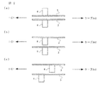
- the Bias-T inductors are close to each other and in the same direction as shown in FIGS. 2 (a) and 2 (b), and each inductor 4 signals. It is arranged in each signal wiring pattern 3 forming a line.
- the same or corresponding parts as those in FIG. 1 will be described with the same reference numerals.
- the inductors 4 may be arranged at distant positions as shown in FIG. 2 (c).
- Patent Document 1 in order to suppress such crosstalk, in an inductor array in which a plurality of inductors are arranged side by side, a technique is provided in which the inductors are arranged so that the flow directions of the magnetic fluxes of the adjacent inductors are orthogonal to each other. It has been disclosed.
- an inducer component having a magnetic shield structure in which the coil winding is covered with a magnetic material as a measure against crosstalk between each inductor.
- the inducer component having a magnetic shield structure the component size is increased by the amount of the shield structure covering the coil winding, and the circuit board 5 cannot be miniaturized.
- an inducer component having a closed magnetic path structure such as a ferrite bead inductor whose outer periphery is molded with a magnetic material.
- the inducer component having a closed magnetic circuit structure can be miniaturized, it is not suitable for the application of transmitting a direct current in the PoC signal transmission system shown in FIG. 1 because the direct current superimposition characteristic is generally poor. ..
- the first inductor to be A second mounting land formed along the second inclined side with one end in contact with an angle where the second signal wiring pattern extending in the extending direction and the second inclined side intersect.
- the axial center direction is tilted in the direction of 90 ° ⁇ 45 ° with respect to the axial center direction of the first inductor, and is oriented perpendicular to the second mounting land, and one electrode terminal is along the second mounting land.
- One of the electrode terminals is connected to the second mounting land, and the inductor mounting structure including the second inductor mounted on the circuit board in the vicinity of the first inductor is configured.
- the first inductor and the second inductor are mounted on the circuit board with their axial center directions tilted in the direction of 90 ° ⁇ 45 °. Therefore, the flow direction of the magnetic flux formed by the first inductor and the flow direction of the magnetic flux formed by the second inductor are substantially orthogonal to each other. Therefore, even if the first inductor and the second inductor are mounted close to the circuit board, it becomes difficult for the magnetic flux formed by the first inductor and the magnetic flux formed by the second inductor to be coupled. The occurrence of crosstalk is suppressed.
- one electrode terminal is located on the first mounting land while the axial center direction is oriented perpendicular to the first mounting land and one electrode terminal is arranged along the first mounting land. It is connected and mounted on the circuit board. Further, the first mounting land is formed along the first inclined side with one end in contact with an angle where the first signal wiring pattern extending in the extending direction and the first inclined side intersect.
- the first inductor one electrode terminal and the first mounting land are mounted on the circuit board, and the first mounting land is formed along the first inclined side. Therefore, the amount of the width of the first mounting land protruding from the width of the first inclined side is much suppressed as compared with the case where the first mounting land is formed at right angles to the signal wiring pattern, and is a small amount. Moreover, the first mounting land is formed so that one end thereof is in contact with an angle at which the first signal wiring pattern and the first inclined side intersect. Therefore, in the embodiment in which the width of the first mounting land protrudes from the width of the first inclined side at one end thereof, the first mounting land formed along the straight line portion of the first signal wiring pattern is the first signal wiring pattern.
- the widened end of the first mounting land is in contact with the end of the first signal wiring pattern at an angle, so that the first mounting land and the first signal are signaled. In a state where the difference in width generated between the two wiring patterns is small, the two are connected.
- the width of the first mounting land becomes larger than the width of the first inclined side, so that the stub effect exerted by the first mounting land is suppressed, and the first inductor is connected to the shunt in the first signal wiring pattern. Even in this case, the signal transmission characteristics are less likely to deteriorate.
- the axial center direction is oriented perpendicular to the second mounting land, one electrode terminal is arranged along the second mounting land, and one electrode terminal is the second mounting land. It is connected to and mounted on the circuit board. Further, the second mounting land is formed along the second inclined side with one end in contact with an angle where the second signal wiring pattern extending in the extending direction and the second inclined side intersect.
- the amount of the width of the second mounting land protruding from the width of the second inclined side is a small amount.
- the widened end end of the second mounting land is at an angle where the second signal wiring pattern and the second inclined side intersect.
- the width of the second mounting land becomes larger than the width of the second inclined side, the stub effect produced by the second mounting land is also suppressed, and the second inductor is connected to the shunt in the second signal wiring pattern. Even in this case, the signal transmission characteristics are less likely to deteriorate.
- first inclined side is formed on the circuit board at an angle of 22.5 ° to 67.5 ° with respect to the extending direction on one side of the extending direction of the first signal wiring pattern.
- the second inclined side has an angle of 22.5 ° to 67.5 ° with respect to the stretching direction on the other side of the stretching direction of the second signal wiring pattern formed alongside the first signal wiring pattern. Tilt and form on the circuit board.
- the inclination angles of the first inclined side and the second inclined side are the first, while maintaining the state in which the axial center directions of the first inductor and the second inductor are inclined to 90 ° ⁇ 45 °.
- the angle is set so that deterioration of the signal transmission characteristics of each high frequency signal transmitted to the signal wiring pattern and the second signal wiring pattern can be suppressed.
- an inductance mounting structure is provided that can suppress the occurrence of crosstalk without having a magnetic shield structure and does not deteriorate the DC superimposition characteristic by having a closed magnetic path structure.
- the present invention The first signal wiring pattern and the second signal wiring pattern formed side by side on the circuit board, and The first mounting land formed along the formation direction of the first signal wiring pattern, With the axial center direction oriented perpendicular to the first mounting land and one electrode terminal arranged along the first mounting land, one electrode terminal is connected to the first mounting land and mounted on the circuit board.
- the first inductor with an inductance value of 0.7 [ ⁇ H] to 3.3 [ ⁇ H] and A second mounting land formed along the formation direction of the second signal wiring pattern, The axial center distance from the first inductor is 2 [mm] to 8 [mm] away, the axial center direction is oriented perpendicular to the second mounting land, and one electrode terminal is on the second mounting land.
- One of the electrode terminals is connected to the second mounting land and mounted on the circuit board while being arranged along the same.
- the inductance value is 0.7 [ ⁇ H] to 3.3 [ ⁇ H], which is the same as that of the first inductor.
- the mounting structure of the inductor including the second inductor of the above was constructed.
- the axial distance between the first inductor and the second inductor having the same inductance value of 0.7 [ ⁇ H] to 3.3 [ ⁇ H] is separated by 2 [mm] to 8 [mm].
- an inductor mounting structure that can be mounted is provided.
- FIG. 6 It is a top view which shows the inductor mounting structure by 1st Embodiment in which the signal wiring pattern in the inductor mounting structure shown in FIG. 6 is in a preferable state. It is a top view which shows the mounting structure of the inductor by the 2nd modification of 1st Embodiment. It is a top view which shows the mounting structure of the inductor according to the 2nd Embodiment of this invention. It is a board mounting diagram at the time of each signal transmission characteristic measurement performed at each axis spacing in order to find the desired axis spacing between inductors in the insulator mounting structure according to the second embodiment. (A) is a graph showing the results of each signal transmission characteristic measurement performed at each axis spacing shown in FIG.
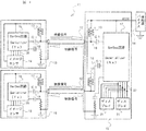
- FIG. 4 is a block diagram showing a schematic configuration of a PoC signal transmission system 11 to which the inductor mounting structure according to the first embodiment of the present invention is applied.
- the PoC signal transmission system 11 uses PoC transmission technology in which a signal and a DC bias power supply are superimposed on one signal line 12 configured by a coaxial cable.
- the PoC signal transmission system 11 uses a Bias-T inductor 13, which is an inductor for separating signal power supplies, to transmit a signal propagating through the signal line 12 and DC5 [V] supplied from the bias supply source 14 to the signal line 12. It is separated from the DC bias power supply.
- the Bias-T inductor 13 passes the DC bias power supply output from the bias supply source 14 to the signal line 12 while preventing the signal from leaking from the signal line 12.
- the SerDes (SerializerDeserializer) circuit 16 formed on each circuit board 15 on the controlled side and the SerDes circuit 17 formed on the circuit board 15 on the control side A signal line 12 is wired to each signal line 12, and a signal is transmitted to each signal line 12.
- the SerDes circuits 16 and 17 serialize the parallel signals sent via the plurality of signal lines 20 and 22 into serial signals and send them to one signal line 12, and one signal. This is a circuit that deserializes a serial signal sent via the line 12 to convert it into a parallel signal, and sends it to a plurality of signal lines 20 and 22.
- the DC bias power supply output from the bias supply source 14 is directly supplied to the SerDes circuit 17, and propagates through each signal line 12 through each Bias-T inductor 13 on the SerDes circuit 17 side.
- the DC bias power supply propagating through each signal line 12 is separated from each signal line 12 through each Bias-T inductor 13 on the SerDes circuit 16 side and supplied to each SerDes circuit 16.
- a capacitor C1 is connected in series between each SerDes circuit 16 and 17 and each signal line 12, and the input of the DC bias power supply propagating through the signal line 12 to each SerDes circuit 16 and 17 is blocked by the capacitor C1. Has been done.
- the high frequency signal propagating through each signal line 12 is transmitted to the SerDes circuits 16 and 17 via the capacitor C1.
- Each Bias-T inductor 13 is connected to each signal wiring pattern 18 between a coaxial cable connector (not shown) provided at the end of the signal line 12 and the capacitor C1.
- the frequency characteristic of the ideal impedance of each Bias-T inductor 13 is 0 [ ⁇ ] at direct current and high impedance at high frequency.
- each SerDes circuit 16 is connected to each SerDes circuit 16 on the controlled side via a plurality of signal lines 20, and each SerDes circuit 16 is input from the image sensor 19 via a plurality of signal lines 20.
- the wideband video signal to be generated is serialized and transmitted to each signal line 12.
- each SerDes circuit 16 acts as a serializer circuit, and becomes a transmitter (Tx) that converts a parallel signal into a serial signal and outputs it.
- each display 21 mounted on the vehicle is connected to the SerDes circuit 17 on the control side via a plurality of signal lines 22, and the SerDes circuit 17 is a serial image transmitted from each SerDes circuit 16 via each signal line 12.
- the signal is deserialized and output to each display 21 via a plurality of signal lines 22.
- the SerDes circuit 17 acts as a deserializer circuit, and becomes a receiver (Rx) that converts a serial signal into an original parallel signal and receives it.
- a control signal propagates from the SerDes circuit 17 to each SerDes circuit 16 side in the opposite direction of each signal line 12, and each image sensor 19 is controlled by the circuit on the display 21 side.
- the SerDes circuit 17 acts as a serializer circuit and becomes a transmitter (Tx) that converts a parallel signal into a serial signal and outputs it.
- each SerDes circuit 16 functions as a deserializer circuit, and serves as a receiver (Rx) that converts a serial signal into an original parallel signal and receives it.
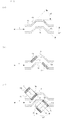
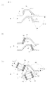
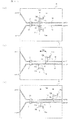
- FIG. 5 is a plan view showing a mounting structure of an inductor according to the first embodiment of the present invention in the circuit board 15 on the control side on which two Bias-T inductors 13 are mounted, and the axial center directions C are orthogonal to each other.
- the mounting structure of each Bias-T inductor 13 to each signal wiring pattern 18 is shown.
- FIG. 6A shows the shape of each signal wiring pattern 18 before mounting each Bias-T inductor 13
- FIG. 3B shows each signal wiring pattern 18 having a first mounting land 31 and a second mounting land 32.
- the formed state, FIG. 3C shows a state in which each Bias-T inductor 13 is mounted on the circuit board 15.
- the first signal wiring pattern 18 located at the upper part of the figure has a first inclination that is inclined to one side of the extension direction H at an angle of 45 ° with respect to the extension direction H. It has sides 18a and is formed on the circuit board 15.
- the second signal wiring pattern 18 located at the lower part of the figure has a second inclined side 18b inclined at an angle of 45 ° with respect to the extending direction H on the other side of the extending direction H, and has a circuit board 15. It is formed on the top side by side with the first signal wiring pattern 18.
- a first mounting land 31 is formed on the first inclined side 18a along the first inclined side 18a. One end of the first mounting land 31 is in contact with an angle where the first signal wiring pattern 18 extending in the extending direction H and the first inclined side 18a intersect.
- a second mounting land 32 is formed on the second inclined side 18b along the second inclined side 18b. One end of the second mounting land 32 is in contact with an angle where the second signal wiring pattern 18 extending in the extending direction H and the second inclined side 18b intersect.
- the axial center direction C of the first Bias-T inductor 13 located at the upper part of the figure is oriented perpendicular to the first mounting land 31, and one of the electrode terminals 13a is the first.
- One of the electrode terminals 13a is connected to the first mounting land 31 and mounted on the circuit board 15 in a state of being arranged along the first mounting land 31.
- the axial direction C of the first Bias-T inductor 13 is oriented perpendicular to the forming direction of the first mounting land 31, and the forming direction of one of the electrode terminals 13a is the forming direction of the first mounting land 31. It is placed along.
- the forming direction of the first mounting land 31 is a direction in which the first mounting land 31 having a rectangular shape extends, and means a direction parallel to the long side of the rectangular shape.
- the forming direction of the electrode terminal 13a is a direction in which the rectangular electrode terminal 13a is stretched, and means a direction parallel to the long side of the rectangular shape.
- the axial center direction C of the second Bias-T inductor 13 located at the lower part of the figure is tilted in a direction of 90 ° with respect to the axial center direction C of the first Bias-T inductor 13.
- One electrode terminal 13a is connected to the second mounting land 32 while one electrode terminal 13a is arranged along the second mounting land 32 so as to be oriented vertically to the second mounting land 32. It is mounted on the circuit board 15 in the vicinity of the Bias-T inductor 13 of the above.
- the axial direction C of the second Bias-T inductor 13 is oriented perpendicular to the forming direction of the second mounting land 32, and the forming direction of one of the electrode terminals 13a is the forming of the second mounting land 32. Arranged along the direction.
- the forming direction of the second mounting land 32 is a direction in which the rectangular-shaped second mounting land 32 extends, and means a direction parallel to the long side of the rectangular shape.
- the other electrode terminal 13b is connected to the power supply line as shown in FIG.
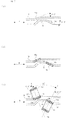
- FIG. 6 shows that in the inductor mounting structure shown in FIG. 5 in which the axial center directions C of the Bias-T inductors 13 are orthogonal to each other, the axial center directions C of the Bias-T inductors 13 are rotated by 22.5 ° in directions away from each other.
- FIG. 3A shows the shape of each signal wiring pattern 18 before mounting each Bias-T inductor 13 used in that state
- FIG. 3B shows each signal wiring shown in FIG.
- FIG. 3A shows the shape of each signal wiring pattern 18 before mounting each Bias-T inductor 13 used in that state
- the first inclined side 18a has a maximum of 67.5 ° with respect to the stretching direction H on one side of the stretching direction H. Tilt with the angle of.
- the second inclined side 18b is inclined toward the other side of the extending direction H at an angle of up to 67.5 ° with respect to the extending direction H.
- a first mounting land 31 is formed on the first inclined side 18a along the first inclined side 18a. Also at this time, one end of the first mounting land 31 is in contact with the corner where the first signal wiring pattern 18 extending in the extending direction H and the first inclined side 18a intersect. Further, a second mounting land 32 is formed on the second inclined side 18b along the second inclined side 18b. Also at this time, one end of the second mounting land 32 is in contact with the corner where the second signal wiring pattern 18 extending in the extending direction H and the second inclined side 18b intersect.
- the first Bias-T inductor 13 located at the upper part of the figure has a maximum axial center direction C of 22. Can be tilted 5 °. Also at this time, the axial center direction C is directed perpendicularly to the first mounting land 31, and one electrode terminal 13a is the first electrode terminal 13a in a state where one electrode terminal 13a is arranged along the first mounting land 31. It is connected to the mounting land 31 and mounted on the circuit board 15. Further, the second Bias-T inductor 13 located at the lower part of the figure is tilted in the axial direction C by a maximum of 22.5 ° clockwise from the state shown in FIG. 5 (c).
- FIG. 7 shows that in the inductor mounting structure shown in FIG. 5 in which the axial center directions C of the Bias-T inductors 13 are orthogonal to each other, the axial center directions C of the Bias-T inductors 13 are rotated by 22.5 ° in a direction approaching each other.
- FIG. 3A shows the shape of each signal wiring pattern 18 before mounting each Bias-T inductor 13 used in that state
- FIG. 3B shows each signal wiring shown in FIG.
- the state where the first mounting land 31 and the second mounting land 32 are formed in the pattern 18, each Bias-T inductor 13 is mounted on each mounting land 31 and 32 shown in FIG. Indicates the state of
- the first inclined side 18a has a minimum of 22.5 with respect to the stretching direction H on one side of the stretching direction H. Tilt at an angle of °.
- the second inclined side 18b is inclined toward the other side of the extending direction H with a minimum angle of 22.5 ° with respect to the extending direction H.
- a first mounting land 31 is formed on the first inclined side 18a along the first inclined side 18a. Also at this time, one end of the first mounting land 31 is in contact with the corner where the first signal wiring pattern 18 extending in the extending direction H and the first inclined side 18a intersect. Further, a second mounting land 32 is formed on the second inclined side 18b along the second inclined side 18b. Also at this time, one end of the second mounting land 32 is in contact with the corner where the second signal wiring pattern 18 extending in the extending direction H and the second inclined side 18b intersect.
- the first Bias-T inductor 13 located at the upper part of the figure has a maximum axial center direction C of 22.5 ° clockwise from the state shown in FIG. 5 (c). Can be tilted. Also at this time, the axial center direction C is directed perpendicularly to the first mounting land 31, and one electrode terminal 13a is the first electrode terminal 13a in a state where one electrode terminal 13a is arranged along the first mounting land 31. It is connected to the mounting land 31 and mounted on the circuit board 15. Further, the second Bias-T inductor 13 located at the lower part of the figure is tilted in the counterclockwise direction by a maximum of 22.5 ° from the state shown in FIG.
- the first Bias-T inductor 13 and the second Bias-T inductor 13 have their axial center directions C within a range of 90 ° ⁇ 45 °. It is mounted on the circuit board 15 in a state of being tilted in the direction of. Therefore, the flow direction of the magnetic flux formed by the first Bias-T inductor 13 and the flow direction of the magnetic flux formed by the second Bias-T inductor 13 are substantially orthogonal to each other.
- one of the electrode terminals 13a is arranged along the first mounting land 31 with the axial center direction C oriented perpendicular to the first mounting land 31.
- the electrode terminal 13a is connected to the first mounting land 31 and mounted on the circuit board 15.
- the first mounting land 31 is formed along the first inclined side 18a with one end in contact with an angle where the first signal wiring pattern 18 extending in the extending direction H and the first inclined side 18a intersect. ..
- the first Bias-T inductor 13 is mounted on the circuit board 15 along the one electrode terminal 13a and the first mounting land 31, and the first mounting land 31 is formed along the first inclined side 18a.
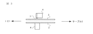
- the amount of the width of the first mounting land 31 protruding from the width of the first inclined side 18a is compared with the case where the mounting land 7 is formed at a right angle to the linear signal wiring pattern 3 as shown in FIG. It is much suppressed and the amount is small.
- the first mounting land 31 is formed so that one end thereof is in contact with an angle at which the first signal wiring pattern 18 and the first inclined side 18a intersect.
- the mode in which the width w1 of the first mounting land 31 protrudes from the width w2 of the first inclined side 18a shown in FIG. 8B is the first signal.
- the width w1 of the first mounting land 31 formed along the straight portion of the wiring pattern 18 is stepped from the width w3 of the first signal wiring pattern 18 in the straight portion of the first signal wiring pattern 18 at both ends thereof. It is different from the aspect that sticks out. That is, as shown in FIG.
- the width w3 of the first signal wiring pattern 18 of the first mounting land 31 Since the widened end is in contact with the end of the first signal wiring pattern 18 at an angle, both of them have a small difference in width between the first mounting land 31 and the first signal wiring pattern 18. It becomes a continuous mode.
- the width w1 of the first mounting land 31 becomes larger than the width w2 of the first inclined side 18a, so that the stub effect exerted by the first mounting land 31 is suppressed, and the first Bias-T inductor 13 becomes the first. Even when the signal wiring pattern 18 is connected to the shunt as shown in FIG. 4, the signal transmission characteristics are less likely to deteriorate.
- the signal transmission characteristics tend to deteriorate.
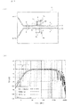
- FIG. 9A a signal wiring pattern 3 for high-speed signal transmission is formed on the circuit board 5, and the mounting directions of the inductors 4 on the circuit board 5 are orthogonal to each other, and FIG. 3 shows.
- the mounting structure of the shown inductor is configured and its signal transmission characteristics are measured, the result shown in the graph of FIG. 9B can be obtained.
- one terminal 4a thereof is formed at a right angle to the signal wiring pattern 3. It is connected to the mounting land 7.
- the other terminal 4b is connected to a so-called solid ground pattern having a large area in the inner layer of the circuit board 5 via a through hole 5a.
- one terminal 4a thereof is formed along the signal wiring pattern 3. It is connected to a mounting land (not shown).
- the other terminal 4b is connected to a ground pattern formed in the inner layer of the circuit board 5 via a through hole 5a.
- a capacitor 6 for cutting off the DC power supply is provided between one terminal 4a of each inductor 4 and each of the ports 1 and 3.
- the signal transmission characteristic S21 in such an inductor mounting structure deteriorates in the high frequency region of the signal as shown in the graph of FIG. 9B. It is considered that this is because the mounting land 7 formed at right angles to the signal wiring pattern 3 acts as a stub.
- the horizontal axis of the graph is frequency [MHz], and the vertical axis is transmission characteristic S21 [dB].
- the transmission characteristic S21 is a characteristic of a signal in which a signal input to the port 1 passes through the port 2, and represents an insertion loss.
- the characteristic line a is a characteristic when each inductor 4 is in an unmounted state (W / O inductor), and the characteristic line b is a characteristic line b of each inductor 4 having a long side of 5 [mm] and a short side of 4 [mm. ] 5040 size inductor, characteristic line c shows the characteristics when each inductor 4 is a 2012 size inductor with a long side of 2 [mm] and a short side of 1.2 [mm]. show.
- the 5040 size and large size inductor 4 shown on the characteristic line b has a worse transmission characteristic S21 than the 2012 size small inductor 4 shown on the characteristic line c in the high frequency region shown by the dotted ellipse 8. do.
- the axial center direction C is directed perpendicularly to the second mounting land 32, and one of the electrode terminals 13a is the first.
- One of the electrode terminals 13a is connected to the second mounting land 32 and mounted on the circuit board 15 in a state of being arranged along the two mounting lands 32.
- the second mounting land 32 is formed along the second inclined side 18b with one end in contact with an angle where the second signal wiring pattern 18 extending in the extending direction H and the second inclined side 18b intersect. ..
- the amount of the width of the second mounting land 32 protruding from the width of the second inclined side 18b is a small amount.
- the mode in which the width of the second mounting land 32 protrudes from the width of the second inclined side 18b at one end thereof is the second mounting land 32 at the angle where the second signal wiring pattern 18 and the second inclined side 18b intersect.
- the second mounting land 32 is similar to the case shown in FIG. 8 (b) by having one end widened from the width of the second signal wiring pattern 18 in contact with the end of the second signal wiring pattern 18 at an angle. In a state where the difference in width between the two and the second signal wiring pattern 18 is small, the two are connected to each other.
- the width of the second mounting land 32 becomes larger than the width of the second inclined side 18b, the stub effect exerted by the second mounting land 32 is also suppressed, and the second Bias-T inductor 13 is used for the second signal wiring. Even when the pattern 18 is connected to the shunt as shown in FIG. 4, the signal transmission characteristics are less likely to deteriorate.
- first inclined side 18a is inclined to one side of the stretching direction H of the first signal wiring pattern 18 at an angle of 22.5 ° to 67.5 ° with respect to the stretching direction H, and is a circuit board. Formed on 15.
- the second inclined side 18b is on the other side of the extension direction H of the second signal wiring pattern 18 formed alongside the first signal wiring pattern 18, from 22.5 ° to 67.5 with respect to the extension direction H. It is formed on the circuit board 15 at an angle of °.
- each inclination angle of the first inclined side 18a and the second inclined side 18b is 90 ° ⁇ 45 ° in each axial direction C of the first Bias-T inductor 13 and the second Bias-T inductor 13.
- the angle is set so that deterioration of the signal transmission characteristics of each high-frequency signal transmitted to the first signal wiring pattern 18 and the second signal wiring pattern 18 can be suppressed while maintaining the tilted state.
- an inductance mounting structure is provided that can suppress the occurrence of crosstalk without having a magnetic shield structure and does not deteriorate the DC superimposition characteristic by having a closed magnetic path structure.
- the flow direction of the magnetic flux formed by the first Bias-T inductor 13 and the second Bias-T inductor 13 are different from each other. It is orthogonal to the flow direction of the formed magnetic flux. Therefore, even if the first Bias-T inductor 13 and the second Bias-T inductor 13 are mounted close to the circuit board 15, the magnetic flux formed by the first Bias-T inductor 13 and the second Bias-T inductor 13 are present.
- the inclination angle of 45 ° of the first inclined side 18a and the second inclined side 18b is such that each axial direction C of the first Bias-T inductor 13 and the second Bias-T inductor 13 is inclined to 90 °. Compared to the case where the deterioration of the signal transmission characteristics of each high frequency signal transmitted to the first signal wiring pattern 18 and the second signal wiring pattern 18 is tilted by 45 ° or more as shown in FIG. It is set to an angle that can be suppressed more.
- the angle of the bent portion / curved portion in the signal wiring pattern 18, that is, the inclined angle of the first inclined side 18a and the second inclined side 18b is 45 ° or less as shown in FIGS. 5 and 7. Is desirable. Therefore, also in the inductor mounting structure shown in FIG. 6, as shown in FIG. 10, the first wiring pattern 18 located at the upper part of the figure is tilted by 22.5 ° in the counterclockwise direction, and the first wiring is performed. It is desirable to set the angle formed by the pattern 18 and the first inclined side 18a to 45 °.
- the second wiring pattern 18 located at the lower part of the figure can be tilted by 22.5 ° in the clockwise direction, and the angle formed by the second wiring pattern 18 and the second inclined side 18b can be set to 45 °. desirable.
- the same or corresponding parts as those in FIG. 6 are designated by the same reference numerals, and the description thereof will be omitted.
- the circuit board 15 is formed on a double-sided board in which a ground layer is formed on an inner layer and components are mounted on both sides, and constitutes an inductor mounting structure.
- the signal wiring pattern 18, the second signal wiring pattern 18, the first mounting land 31, the second mounting land 32, the first Bias-T inductor 13, and the second Bias-T inductor 13 are the circuit boards 15. It may be configured to be formed on both sides respectively.
- An inductor mounting structure for a plurality of signal wiring patterns 18 is configured on both sides of the circuit board 15, which suppresses the stub effect produced by the circuit board and makes it difficult for the signal transmission characteristics to deteriorate.
- mutual crosstalk is reduced by the ground layer formed solidly on the inner layer of the circuit board 15.
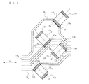
- the mounting structure of the inductor according to the second modified example four signal wiring pattern 18 1, 18 2, 18 3, 18 4 to four Bias-T inductor 13 1, 13 2, 13 3, 13 4 are connected
- the only difference is that the inductor mounting structure according to the first embodiment is described above.
- Two signal wiring pattern 18 1, 18 2 into two Bias-T inductor 13 1, 13 configuration 2 is connected, first the first in an embodiment and second respective signal wiring patterns 18 described above, It is the same as the mounting structure of the inductor in which the first and second Bias-T inductors 13 and 13 are connected to 18.
- the inductor mounting structure according to the second modification has a third inclined side 18a that is inclined at an angle of 22.5 ° to 67.5 ° with respect to the stretching direction H on one side of the stretching direction H.
- a fourth inclined side 18b inclined at an angle of 5 °, and a fourth signal wiring pattern 18 4 are formed side by side in the third signal wiring pattern 18 3 on the circuit board 15.
- a third mounting land 31 is formed on the third inclined side 18a along the third inclined side 18a.
- the third mounting land 31 includes a third signal wiring pattern 18 3 extending in the extension direction H and the third inclined side 18a is in contact with one end at the corner crossing, it is formed.
- the axial center direction C is tilted in a direction of 90 ° ⁇ 45 ° with respect to the axial center direction of the second Bias-T inductor 13 2, and the third mounting land 31
- One electrode terminal 13a is connected to the third mounting land 31 while one electrode terminal 13a is arranged along the third mounting land 31 so as to be oriented vertically to the second Bias-T inductor. It mounted on the circuit board 15 in the 13 2 near the.
- a fourth mounting land 32 is formed on the fourth inclined side 18b along the fourth inclined side 18b.
- Fourth Bias-T inductor 13 4, axially C is tilted in the direction of 90 ° ⁇ 45 ° with respect to the third Bias-T inductor 13 3 in the axial direction C, and the fourth mounting land
- One electrode terminal 13a is connected to the fourth mounting land 32 while one electrode terminal 13a is arranged along the fourth mounting land 32 so as to be oriented vertically to the 32, and the third Bias-T It mounted on the circuit board 15 in the vicinity of the inductor 13 3.
- the third signal wiring pattern 18 3 and the fourth signal arranged in the first signal wiring pattern 18 1 and the second signal wiring pattern 18 2 also the wiring pattern 18 4, occurrence of crosstalk, and is suppressed stub effect the mounting land 31 is achieved, in the hard state degradation of signal transmission characteristics, the third and fourth respective Bias-T of the inductor 13 3, 13 4 can be implemented parallel to the 2 first and second respective Bias-T inductor 13 1, 13. Further, by extending this idea, even when each Bias-T inductor 13 is mounted on four or more signal wiring patterns 18, the same effect can be obtained by similarly applying this technique. An inductor mounting structure is provided.
- FIG. 12 is a plan view showing a mounting structure of an inductor according to the second embodiment of the present invention.
- FIG. 3A shows an inductor mounting structure according to the second embodiment when each Bias-T inductor 13 is connected to each parallel signal wiring pattern 18, and
- FIG. 3B shows each Bias-T inductor 13. Shows the mounting structure of the inductor according to the second embodiment when is connected to each signal wiring pattern 18 having a bent portion.
- the same or corresponding parts as those in FIGS. 5 to 7 will be described with the same reference numerals.
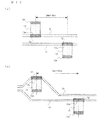
- the first signal wiring pattern 18 and the second signal wiring pattern 18 formed side by side on the circuit board 15 are in the forming direction of the first signal wiring pattern 18.
- a first mounting land 31 formed along the line and a second mounting land 32 formed along the forming direction of the second signal wiring pattern 18 are formed.
- the axial center direction C is oriented perpendicular to the first mounting land 31, and one of the electrode terminals 13a is arranged along the first mounting land 31. Then, one of the electrode terminals 13a is connected to the first mounting land 31 and mounted on the circuit board 15.
- the axial center direction C is oriented perpendicular to the second mounting land 32, and one electrode terminal 13a is arranged along the second mounting land 32.
- one of the electrode terminals 13a is connected to the second mounting land 32 and mounted on the circuit board 15.
- the other electrode terminal 13b of each of the first and second Bias-T inductors 13 is connected to the power supply line as shown in FIG.
- Each of the first and second Bias-T inductors 13 has an inductance value of 0.7 [ ⁇ H] to 3 which can be used in a PoC signal transmission system configured by using a sardine circuit as shown in FIG. .3 Set to the same value within the range of [ ⁇ H]. Further, the first and second Bias-T inductors 13 are provided at positions where the axial center spacing is 2 [mm] to 8 [mm] apart.
- the first Bias-T inductor 13 and the second Bias-T inductor having the same inductance value of 0.7 [ ⁇ H] to 3.3 [ ⁇ H].
- One of the electrode terminals 13a is formed along the first signal wiring pattern 18 and the second signal wiring pattern 18 with the axial center distance from 13 at a position separated from each other by 2 [mm] to 8 [mm].
- Each Bias-T inductor 13 can be mounted on the circuit board 15 in a state where the signal transmission characteristics are not easily deteriorated. Further, each Bias-T inductor 13 can be mounted in the optimum component arrangement in consideration of crosstalk, which can contribute to the miniaturization of the circuit board 15.
- each signal wiring pattern 18 is formed on the circuit board 15, and the axial center spacing of each inductor 13 is 0 [mm] and 4 [mm, respectively. ], 8 [mm]
- the signal transmission characteristics of the mounting structures of the inductors configured at a distance were measured, and the results shown in the graph of FIG. 14 were obtained.
- Each of the inductors 13 in each of the segments (a), (b), and (c) of FIG. 13 has one terminal 13a connected to a mounting land (not shown) formed along the signal wiring pattern 18. ..
- the other terminal 13b is connected to a ground pattern formed in the inner layer of the circuit board 5 via a through hole 15a.
- a capacitor C1 for cutting off the DC power supply is provided between one terminal 13a of each inductor 13 and each of the ports 1 and 3.
- the graph of FIG. 14A is a result of measuring the signal transmission characteristics of the mounting structure shown in FIGS. 13A, 13B, and 13C for each inductor 13 having an inductance value of 1.5 [ ⁇ H].
- the graph of 14 (b) shows the results of measuring the signal transmission characteristics of the mounting structure shown in FIGS. 13 (a), 13 (b), and (c) for each inductor 13 having an inductance value of 2.2 [ ⁇ H].
- the signal transmission characteristic was measured by measuring the crosstalk characteristic S31 that evaluates the amount of signal leakage between adjacent ports 1 and 3.
- the horizontal axis of each graph is frequency [MHz], and the vertical axis is crosstalk characteristic S31 [dB].
- the characteristic line d of the alternate long and short dash line in each graph indicates the axial spacing of each inductor 13 to 0 [mm] as shown in FIG. 13 (a)
- the characteristic line e of the dotted line indicates the axial spacing of each inductor 13 (FIG. 13).
- the characteristic f of the solid line is 4 [mm] as shown in b), and is the measurement result when the axial center spacing of each inductor 13 is set to 8 [mm] as shown in FIG. 13 (c).
- the measurement results having a frequency of 50 [MHz] or higher are not measured by the crosstalk of each inductor 13, but are measured by the crosstalk of the circuit board 15 itself, and are therefore ignored. , 50 [MHz] or less.
- both the measurement results shown in FIG. 14 (a) and the measurement results shown in FIG. 14 (b) indicate the axial center spacing. This is the case when the frequency is 4 [mm] or more as shown in FIGS. 13 (b) and 13 (c).
- the number of turns of the inductor 13 is increased in order to increase the inductance value, it is necessary to further increase the axial spacing of each inductor 13, and conversely, the number of turns of the inductor 13 should be reduced in order to decrease the inductance value.
- the distance between the axes of the inductors 13 can be made close to each other.
- the inductance value that can be used in the PoC signal transmission system configured using the SerDes circuit is in the range of 0.7 [ ⁇ H] to 3.3 [ ⁇ H] as described above. Therefore, since the axial center spacing to be taken when the inductance value is 1.5 [ ⁇ H] is 4 [mm] as described above, the inductance value is 0.7 [, which is about half of 1.5 [ ⁇ H].
- the axis spacing to be taken when ⁇ H] is 2 [mm], which is half of 4 [mm], and the axis to be taken when the inductance value is 3.3 [ ⁇ H], which is about twice that of 1.5 [ ⁇ H].
- the interval is 8 [mm], which is twice 4 [mm].
- the fifth Bias-T inductor 13 and the sixth Bias-T inductor 13 whose axial center direction C cannot be tilted in the direction of 90 ° ⁇ 45 ° cannot be tilted.
- the inductance values thereof are set to 0.7 [ ⁇ H] to 3.3 [ ⁇ H]
- the axial center spacing is set at a position separated by 2 [mm] to 8 [mm]
- the fifth Each Bias-T inductor 13 is connected to the signal wiring pattern 18 and the sixth signal wiring pattern 18 via the fifth mounting land 31 and the sixth mounting land 32 as in the inductor mounting structure according to the second embodiment.
- the occurrence of crosstalk between the Bias-T inductors 13 and the stub effect of the mounting lands 31 and 32 are suppressed, and the signal transmission characteristics are less likely to deteriorate.
- the inductor according to the first embodiment and the first and second modifications including the first and second signal wiring patterns 18 described above, or the third and fourth signal wiring patterns 18 in addition to them.
- the fifth signal wiring pattern 18 and the sixth signal wiring pattern 18 formed side by side with the second signal wiring pattern 18 on the circuit board 15, and the formation direction of the fifth signal wiring pattern 18 A fifth mounting land 31 formed along the line and a sixth mounting land 32 formed along the forming direction of the sixth signal wiring pattern 18 are further formed.
- the fifth Bias-T inductor 13 having an inductance value of 0.7 [ ⁇ H] to 3.3 [ ⁇ H] and the same 0.7 [] as the fifth Bias-T inductor 13 having an inductance value.
- a sixth Bias-T inductor 13 of ⁇ H] to 3.3 [ ⁇ H] is provided.
- the axial center direction C is oriented perpendicular to the fifth mounting land 31, and one of the electrode terminals 13a is arranged along the fifth mounting land 31.
- the electrode terminal 13a of the above is connected to the fifth mounting land 31 and mounted on the circuit board 15.
- the sixth Bias-T inductor 13 is provided at a position where the axial center distance from the fifth Bias-T inductor 13 is 2 [mm] to 8 [mm] apart, and the axial center direction C is the sixth mounting land 32.
- One electrode terminal 13a is connected to the sixth mounting land 32 and mounted on the circuit board 15 in a state where one electrode terminal 13a is arranged along the sixth mounting land 32.
- the inductor mounting structure is configured in this way, as described above, in the inductor mounting structure according to the first embodiment, the fifth Bias in which the axial center direction C cannot be tilted in the direction of 90 ° ⁇ 45 ° cannot be tilted. Even if the -T inductor 13 and the sixth Bias-T inductor 13 are present, the same operation and effect as the inductor mounting structure according to the first embodiment can be obtained.
- the inductor mounting structure As shown in FIG. 4, the inductor mounting structure according to each of the above-described embodiments and modifications is configured on a circuit board 15 on which a serializer circuit and a deserializer circuit to which a plurality of signal lines 12 are connected are formed. Therefore, an inductor mounting structure suitable for the Bias-T inductor 13 in the PoC signal transmission system 11 including two or more signal lines 12 is provided.
- the serializer circuit converts the video signal of the vehicle-mounted camera from the parallel signal to the serial signal
- the deserializer circuit converts the video signal of the vehicle-mounted camera into a serial signal. Converts a video signal to a parallel signal. Therefore, an inductor mounting structure suitable for the Bias-T inductor 13 in an in-vehicle system using PoC signal transmission, which includes two or more signal lines 12 for transmitting video signals of an in-vehicle camera, is provided.
- PoC signal transmission system 12 20 , 22 ... Signal line 13, 13 1 , 13 2, 13 3 , 13 4 ... Bias-T inductor (inductor for signal power supply separation) 14 ... Bias supply source 15 ... Circuit board 16, 17 ... SerDes circuit (serializer circuit, deserializer circuit) 18 , 18 1 , 18 2 , 18 3 , 18 4 ... Signal wiring pattern 18a ... 1st inclined side 18b ... 2nd inclined side 19 ... Image sensor 21 ... Display 31 ... 1st mounting land 32 ... 2nd mounting land C1 ... Capacitor
Landscapes
- Engineering & Computer Science (AREA)
- Microelectronics & Electronic Packaging (AREA)
- Physics & Mathematics (AREA)
- Electromagnetism (AREA)
- Coils Or Transformers For Communication (AREA)
- Structures For Mounting Electric Components On Printed Circuit Boards (AREA)
Abstract
クロストークの発生および実装ランドが奏するスタブ効果が抑制されて、信号伝送特性の劣化がし難い状態で、各インダクタを実装できるインダクタの実装構造を提供する。第1のBias-Tインダクタ13は、軸心方向Cが第1実装ランド31に垂直に向けられ、一方の電極端子13aが第1実装ランド31に沿った状態で、一方の電極端子13aが第1実装ランド31に接続されて、回路基板15に実装される。また、第2のBias-Tインダクタ13は、軸心方向Cが第1のBias-Tインダクタ13の軸心方向Cに対して90°傾けられ、かつ、第2実装ランド32に垂直に向けられて、一方の電極端子13aが第2実装ランド32に沿った状態で、一方の電極端子13aが第2実装ランド32に接続されて、第1のBias-Tインダクタ13の近傍における回路基板15に実装される。
Description
本発明は、回路基板における複数本の信号配線パターンへのインダクタの実装構造に関するものである。
従来、1本の同軸ケーブルに信号と直流バイアス電源とを重畳させて通信を行うPoC(Power Over Coax.)と呼ばれる信号伝送技術がある。この技術を使った信号伝送回路には、Bias-Tインダクタと呼ばれる信号電源分離用インダクタが用いられ、このインダクタにより、信号線を伝搬する信号と、バイアス供給源から信号線へ供給される直流バイアス電源とが分離される。
最近、このPoCと呼ばれる信号伝送技術により伝送される信号が多く、図1に示す回路ブロック図のように、1つの信号伝送用IC1に、複数本の同軸ケーブル2によって伝送される信号が入出力される。したがって、1つの信号伝送用IC1に接続される複数本の信号ライン3の各々に、Bias-Tインダクタ4を設ける必要があり、複数個のBias-Tインダクタ4が信号伝送用IC1と共に1つの回路基板5に実装される。各Bias-Tインダクタ4は一方の端子が信号ライン3、他方の端子が信号伝送用IC1への電源供給ラインに接続される。なお、各信号ライン3は、直流電源遮断用のコンデンサ6を介して信号伝送用IC1に接続される。
通常、2本以上の信号ラインを含むPoC信号伝送のシステムにおけるBias-Tインダクタは、図2(a)や図2(b)に示すように互いに近接して同じ向きに、各インダクタ4が信号ラインを形成する各信号配線パターン3に配置される。なお、図2において図1と同一または相当する部分には同一符号を付して説明する。また、回路基板5上における部品レイアウトの問題を回避するため、図2(c)に示すように各インダクタ4が離れた位置に配置される場合もある。
一方、回路基板5の小型化の観点から、Bias-Tインダクタ4の回路基板5における実装領域を可能な限り小さくする必要がある。この場合、近接配置される複数個のインダクタ4間におけるクロストークが問題となる。
特許文献1には、このようなクロストークを抑制するため、複数個のインダクタを並設したインダクタアレイにおいて、隣接する各インダクタの磁束の流れ方向が互いに直交するよう、各インダクタを配置する技術が開示されている。
図2(a),(b)に示すように各インダクタ4が近接配置される場合において、特許文献1に開示された技術を適用して、図3に示すように、各インダクタ4の回路基板5への実装の向きを互いに直交させることは可能である。しかしながら、一方のインダクタ4を他方のインダクタ4に直交配置させるには、信号配線パターン3に垂直に実装ランド7を設け、インダクタ4の一方の電極端子をその実装ランド7に接続させる必要がある。したがって、これらのインダクタ4を、PoC信号伝送システムにおける信号電源分離用インダクタとして用いて、図1に示すように高速信号伝送用の信号配線パターン3にシャントに接続する場合、実装ランド7が信号配線パターン3にスタブとして接続された状態になり、信号伝送特性の劣化につながる。
また、各インダクタ間のクロストーク対策として、コイル巻線を磁性体で覆った磁気シールド構造を有したインダタクタ部品を用いることも、考えられる。しかしながら、磁気シールド構造を有したインダタクタ部品は、コイル巻線を覆うシールド構造体の分だけ部品サイズが大型化し、回路基板5の小型化が図れない。
また、磁性体で外周がモールドされたフェライトビーズインダクタのように閉磁路構造を有したインダタクタ部品を用いることも、考えられる。しかしながら、閉磁路構造を有したインダタクタ部品は、小型化は可能であるが、一般的に直流重畳特性が悪いため、図1に示すPoC信号伝送システムにおいて直流電流を伝送する用途には向いていない。
本発明はこのような課題を解消するためになされたもので、
延伸方向の一方側に延伸方向に対して22.5°から67.5°の角度を持って傾く第1傾斜辺を有して回路基板上に形成される第1の信号配線パターンと、
延伸方向の他方側に延伸方向に対して22.5°から67.5°の角度を持って傾く第2傾斜辺を有して回路基板上に第1の信号配線パターンに並んで形成される第2の信号配線パターンと、
延伸方向に延伸する第1の信号配線パターンと第1傾斜辺とが交差する角に一端が接して第1傾斜辺に沿って形成された第1実装ランドと、
軸心方向が第1実装ランドに垂直に向けられ、一方の電極端子が第1実装ランドに沿って配置された状態で、一方の電極端子が第1実装ランドに接続されて、回路基板に実装される第1のインダクタと、
延伸方向に延伸する第2の信号配線パターンと第2傾斜辺とが交差する角に一端が接して第2傾斜辺に沿って形成された第2実装ランドと、
軸心方向が第1のインダクタの軸心方向に対して90°±45°の方向に傾けられ、かつ、第2実装ランドに垂直に向けられて、一方の電極端子が第2実装ランドに沿って配置された状態で、一方の電極端子が第2実装ランドに接続されて、第1のインダクタの近傍における回路基板に実装される第2のインダクタと
を備えるインダクタの実装構造を構成した。
延伸方向の一方側に延伸方向に対して22.5°から67.5°の角度を持って傾く第1傾斜辺を有して回路基板上に形成される第1の信号配線パターンと、
延伸方向の他方側に延伸方向に対して22.5°から67.5°の角度を持って傾く第2傾斜辺を有して回路基板上に第1の信号配線パターンに並んで形成される第2の信号配線パターンと、
延伸方向に延伸する第1の信号配線パターンと第1傾斜辺とが交差する角に一端が接して第1傾斜辺に沿って形成された第1実装ランドと、
軸心方向が第1実装ランドに垂直に向けられ、一方の電極端子が第1実装ランドに沿って配置された状態で、一方の電極端子が第1実装ランドに接続されて、回路基板に実装される第1のインダクタと、
延伸方向に延伸する第2の信号配線パターンと第2傾斜辺とが交差する角に一端が接して第2傾斜辺に沿って形成された第2実装ランドと、
軸心方向が第1のインダクタの軸心方向に対して90°±45°の方向に傾けられ、かつ、第2実装ランドに垂直に向けられて、一方の電極端子が第2実装ランドに沿って配置された状態で、一方の電極端子が第2実装ランドに接続されて、第1のインダクタの近傍における回路基板に実装される第2のインダクタと
を備えるインダクタの実装構造を構成した。
本構成によれば、第1のインダクタと第2のインダクタとは、互いの軸心方向が90°±45°の方向に傾けられた状態で、回路基板に実装される。したがって、第1のインダクタが形成する磁束の流れ方向と、第2のインダクタとが形成する磁束の流れ方向とは、ほぼ直交する。このため、第1のインダクタと第2のインダクタとは、回路基板に近接して実装されても、第1のインダクタが形成する磁束と第2のインダクタが形成する磁束とが結合し難くなり、クロストークの発生が抑制される。
また、第1のインダクタは、軸心方向が第1実装ランドに垂直に向けられ、一方の電極端子が第1実装ランドに沿って配置された状態で、一方の電極端子が第1実装ランドに接続されて、回路基板に実装される。また、第1実装ランドは、延伸方向に延伸する第1の信号配線パターンと第1傾斜辺とが交差する角に一端が接して、第1傾斜辺に沿って形成される。
したがって、第1のインダクタは、一方の電極端子と第1実装ランドとが沿って回路基板に実装され、第1実装ランドは第1傾斜辺に沿って形成される。このため、第1実装ランドの幅が第1傾斜辺の幅からはみ出る量は、第1実装ランドが信号配線パターンに直角に形成される場合に比較して遙かに抑制され、僅かな量となる。しかも、第1実装ランドは、その一端が、第1の信号配線パターンと第1傾斜辺とが交差する角に接して、形成される。このため、第1実装ランドの幅がその一端で第1傾斜辺の幅からはみ出る態様は、第1の信号配線パターンの直線部に沿って形成された第1実装ランドが第1の信号配線パターンの直線部において階段状にはみ出る態様と異なり、その角において、第1実装ランドの拡幅した一端が第1の信号配線パターンの端部と斜めに接することで、第1実装ランドと第1の信号配線パターンの両者の間に生じる幅の差が少ない状態で、両者が連なる態様となる。
この結果、第1実装ランドの幅が第1傾斜辺の幅より大きくなることで第1実装ランドが奏するスタブ効果は抑制され、第1のインダクタが第1の信号配線パターンにシャントに接続される場合であっても、信号伝送特性は劣化し難くなる。
また、第2のインダクタは、軸心方向が第2実装ランドに垂直に向けられて、一方の電極端子が第2実装ランドに沿って配置された状態で、一方の電極端子が第2実装ランドに接続されて、回路基板に実装される。また、第2実装ランドは、延伸方向に延伸する第2の信号配線パターンと第2傾斜辺とが交差する角に一端が接して、第2傾斜辺に沿って形成される。
したがって、上記の第1の実装ランドと同様に、第2実装ランドの幅が第2傾斜辺の幅からはみ出る量は、僅かな量となる。しかも、第2実装ランドの幅がその一端で第2傾斜辺の幅からはみ出る態様は、第2の信号配線パターンと第2傾斜辺とが交差する角において、第2実装ランドの拡幅した一端が第2の信号配線パターンの端部と斜めに接することで、第2実装ランドと第2の信号配線パターンの両者の間に生じる幅の差が少ない状態で、両者が連なる態様となる。このため、第2実装ランドの幅が第2傾斜辺の幅より大きくなることで第2実装ランドが奏するスタブ効果も抑制され、第2のインダクタが第2の信号配線パターンにシャントに接続される場合においても、信号伝送特性は劣化し難くなる。
また、第1傾斜辺は、第1の信号配線パターンの延伸方向の一方側に、延伸方向に対して22.5°から67.5°の角度を持って傾いて、回路基板上に形成される。第2傾斜辺は、第1の信号配線パターンに並んで形成される第2の信号配線パターンの延伸方向の他方側に、延伸方向に対して22.5°から67.5°の角度を持って傾いて、回路基板上に形成される。
このため、第1傾斜辺および第2傾斜辺の各傾斜角度は、第1のインダクタと第2のインダクタとの各軸心方向を90°±45°に傾いた状態を保ちながら、第1の信号配線パターンおよび第2の信号配線パターンに伝送される各高周波信号の信号伝送特性の劣化を抑制できる角度に設定される。この結果、磁気シールド構造を有することなく、クロストークの発生を抑制でき、しかも、閉磁路構造を有することで直流重畳特性が悪化することのない、インダクタンスの実装構造が提供される。
また、本発明は、
回路基板上に並んで形成される第1の信号配線パターンおよび第2の信号配線パターンと、
第1の信号配線パターンの形成方向に沿って形成された第1実装ランドと、
軸心方向が第1実装ランドに垂直に向けられ、一方の電極端子が第1実装ランドに沿って配置された状態で、一方の電極端子が第1実装ランドに接続されて回路基板に実装される、インダクタンス値が0.7[μH]~3.3[μH]の第1のインダクタと、
第2の信号配線パターンの形成方向に沿って形成された第2実装ランドと、
第1のインダクタとの軸心間隔が2[mm]~8[mm]離れた位置に設けられ、軸心方向が第2実装ランドに垂直に向けられ、一方の電極端子が第2実装ランドに沿って配置された状態で、一方の電極端子が第2実装ランドに接続されて回路基板に実装される、インダクタンス値が第1のインダクタと同じ0.7[μH]~3.3[μH]の第2のインダクタと
を備えるインダクタの実装構造を構成した。
回路基板上に並んで形成される第1の信号配線パターンおよび第2の信号配線パターンと、
第1の信号配線パターンの形成方向に沿って形成された第1実装ランドと、
軸心方向が第1実装ランドに垂直に向けられ、一方の電極端子が第1実装ランドに沿って配置された状態で、一方の電極端子が第1実装ランドに接続されて回路基板に実装される、インダクタンス値が0.7[μH]~3.3[μH]の第1のインダクタと、
第2の信号配線パターンの形成方向に沿って形成された第2実装ランドと、
第1のインダクタとの軸心間隔が2[mm]~8[mm]離れた位置に設けられ、軸心方向が第2実装ランドに垂直に向けられ、一方の電極端子が第2実装ランドに沿って配置された状態で、一方の電極端子が第2実装ランドに接続されて回路基板に実装される、インダクタンス値が第1のインダクタと同じ0.7[μH]~3.3[μH]の第2のインダクタと
を備えるインダクタの実装構造を構成した。
本構成によれば、インダクタンス値が同じ0.7[μH]~3.3[μH]の第1のインダクタと第2のインダクタとの軸心間隔を2[mm]~8[mm]離れた位置にして、それぞれの一方の電極端子を、第1の信号配線パターンおよび第2の信号配線パターンに沿って形成された第1実装ランドおよび第2実装ランドにそれぞれ接続することで、クロストークの発生、および、実装ランドが奏するスタブ効果が抑制されて、信号伝送特性の劣化がし難い状態で、各インダクタを回路基板に実装することができる。
本発明によれば、複数のインダクタが近接配置される場合においても、クロストークの発生、および、実装ランドが奏するスタブ効果が抑制されて、信号伝送特性の劣化がし難い状態で、各インダクタを実装することのできるインダクタの実装構造が提供される。
次に、本発明によるインダクタの実装構造を実施するための形態について、説明する。
図4は、本発明の第1実施形態によるインダクタの実装構造が適用されるPoC信号伝送システム11の概略構成を示すブロック図である。
PoC信号伝送システム11は、同軸ケーブルによって構成される1本の信号線12に信号と直流バイアス電源とを重畳させるPoC伝送技術を使っている。このPoC信号伝送システム11は、信号電源分離用インダクタであるBias-Tインダクタ13を用いて、信号線12を伝搬する信号と、バイアス供給源14から信号線12へ供給されるDC5[V]の直流バイアス電源とを分離している。Bias-Tインダクタ13は、信号線12から信号が漏れるのを阻止しつつ、バイアス供給源14から出力される直流バイアス電源を信号線12へ通す。
本実施形態のPoC信号伝送システム11は、被制御側の各回路基板15に形成されるSerDes(Serializer Deserializer:サーデス)回路16と、制御側の回路基板15に形成されるSerDes回路17との間にそれぞれ信号線12が配線され、各信号線12に信号が伝送される。SerDes回路16,17は、複数本の信号線20,22を経由して送られて来たパラレル信号をシリアル信号にシリアライズ(Serialize)して1本の信号線12へ送出し、1本の信号線12を経由して送られて来たシリアル信号をデシリアライズ(Deserialize)してパラレル信号に変換し、複数本の信号線20,22へ送出する回路である。
バイアス供給源14から出力される直流バイアス電源は、SerDes回路17に直接供給されると共に、SerDes回路17側の各Bias-Tインダクタ13を通って各信号線12を伝搬する。各信号線12を伝搬した直流バイアス電源は、SerDes回路16側の各Bias-Tインダクタ13を通って各信号線12から分離して、各SerDes回路16へ供給される。各SerDes回路16,17と各信号線12との間にはそれぞれコンデンサC1が直列に接続され、信号線12を伝搬する直流バイアス電源の各SerDes回路16,17への入力が、コンデンサC1によって阻止されている。各信号線12を伝搬する高周波の信号はコンデンサC1を経由して各SerDes回路16,17へ伝えられる。各Bias-Tインダクタ13は、信号線12の端部に設けられる図示しない同軸ケーブルコネクタとコンデンサC1との間の各信号配線パターン18に接続されている。各Bias-Tインダクタ13の理想的なインピーダンスの周波数特性は、直流では0[Ω]、高周波ではハイインピーダンスを示す特性である。
被制御側の各SerDes回路16には例えば車載カメラのイメージセンサ19が複数本の信号線20を介して接続され、各SerDes回路16は、イメージセンサ19から複数本の信号線20を介して入力される広帯域の映像信号をシリアライズして各信号線12へ送出する。この際、各SerDes回路16は、シリアライザ(Serializer)回路として働き、パラレル信号をシリアル信号に変換して出力する送信器(Tx)となる。
制御側のSerDes回路17には例えば車載される各ディスプレイ21が複数本の信号線22介して接続され、SerDes回路17は、各信号線12を介して各SerDes回路16から送られてくるシリアル映像信号をデシリアライズして、複数本の信号線22を介して各ディスプレイ21へ出力する。この際、SerDes回路17は、デシリアライザ(Deserializer)回路として働き、シリアル信号を元のパラレル信号に変換して受信する受信器(Rx)となる。
また、SerDes回路17から各SerDes回路16側へ、各信号線12を逆方向へ制御信号が伝搬し、各イメージセンサ19がディスプレイ21側の回路によって制御される。この際、SerDes回路17はシリアライザ回路として働き、パラレル信号をシリアル信号に変換して出力する送信器(Tx)となる。また、各SerDes回路16は、デシリアライザ(Deserializer)回路として働き、シリアル信号を元のパラレル信号に変換して受信する受信器(Rx)となる。
図5は、2個のBias-Tインダクタ13が実装される制御側の回路基板15における、本発明の第1実施形態によるインダクタの実装構造を示す平面図であり、軸心方向Cが直交した各Bias-Tインダクタ13の各信号配線パターン18への実装構造を示している。同図(a)は、各Bias-Tインダクタ13の実装前における各信号配線パターン18の形状、同図(b)は、各信号配線パターン18に第1実装ランド31,第2実装ランド32が形成された状態、同図(c)は、回路基板15に各Bias-Tインダクタ13が実装された状態を示す。
同図(a)に示すように、図の上方に位置する第1の信号配線パターン18は、その延伸方向Hの一方側に延伸方向Hに対して45°の角度を持って傾く第1傾斜辺18aを有して、回路基板15上に形成されている。図の下方に位置する第2の信号配線パターン18は、その延伸方向Hの他方側に延伸方向Hに対して45°の角度を持って傾く第2傾斜辺18bを有して、回路基板15上に第1の信号配線パターン18に並んで形成されている。
同図(b)に示すように、第1傾斜辺18aには第1実装ランド31が第1傾斜辺18aに沿って形成される。第1実装ランド31の一端は、延伸方向Hに延伸する第1の信号配線パターン18と第1傾斜辺18aとが交差する角に接している。また、第2傾斜辺18bには第2実装ランド32が第2傾斜辺18bに沿って形成される。第2実装ランド32の一端は、延伸方向Hに延伸する第2の信号配線パターン18と第2傾斜辺18bとが交差する角に接している。
同図(c)に示すように、図の上方に位置する第1のBias-Tインダクタ13は、その軸心方向Cが第1実装ランド31に垂直に向けられ、一方の電極端子13aが第1実装ランド31に沿って配置された状態で、一方の電極端子13aが第1実装ランド31に接続されて、回路基板15に実装される。第1のBias-Tインダクタ13の軸心方向Cは、詳細には、第1実装ランド31の形成方向に垂直に向けられ、一方の電極端子13aの形成方向が第1実装ランド31の形成方向に沿って配置される。ここで、第1実装ランド31の形成方向とは、矩形形状をした第1実装ランド31が延伸する方向であり、その矩形形状の長辺に平行な方向を意味する。同様に、電極端子13aの形成方向とは、矩形形状をした電極端子13aが延伸する方向であり、その矩形形状の長辺に平行な方向を意味する。
また、図の下方に位置する第2のBias-Tインダクタ13は、その軸心方向Cが第1のBias-Tインダクタ13の軸心方向Cに対して90°の方向に傾けられ、かつ、第2実装ランド32に垂直に向けられて、一方の電極端子13aが第2実装ランド32に沿って配置された状態で、一方の電極端子13aが第2実装ランド32に接続されて、第1のBias-Tインダクタ13の近傍における回路基板15に実装される。第2のBias-Tインダクタ13の軸心方向Cは、詳細には、第2実装ランド32の形成方向に垂直に向けられて、一方の電極端子13aの形成方向が第2実装ランド32の形成方向に沿って配置される。ここで、第2実装ランド32の形成方向とは、矩形形状をした第2実装ランド32が延伸する方向であり、その矩形形状の長辺に平行な方向を意味する。第1および第2の各Bias-Tインダクタ13は、他方の電極端子13bが図4に示すように電源ラインに接続される。
図6は、各Bias-Tインダクタ13の軸心方向Cが直交した図5に示すインダクタの実装構造において、各Bias-Tインダクタ13の軸心方向Cを互いに離れる方向に22.5°ずつ回転させて、各Bias-Tインダクタ13の軸心方向Cが90°+45°(=135°)傾けられた状態における、本発明の第1実施形態によるインダクタの実装構造を示している。本発明の第1実施形態によるインダクタの実装構造は、各Bias-Tインダクタ13の軸心方向Cが図6に示すように最大で90°+45°(=135°)傾けられる。同図(a)は、その状態のときに用いられる、各Bias-Tインダクタ13の実装前における各信号配線パターン18の形状、同図(b)は、同図(a)に示す各信号配線パターン18に第1実装ランド31,第2実装ランド32が形成された状態、同図(c)は、同図(b)に示す各実装ランド31,32に各Bias-Tインダクタ13が実装された状態を示す。
同図(a)に示すように、図の上方に位置する第1の信号配線パターン18は、第1傾斜辺18aが、延伸方向Hの一方側に延伸方向Hに対して最大67.5°の角度を持って傾く。図の下方に位置する第2の信号配線パターン18は、第2傾斜辺18bが、延伸方向Hの他方側に延伸方向Hに対して最大67.5°の角度を持って傾く。
同図(b)に示すように、第1傾斜辺18aには第1実装ランド31が第1傾斜辺18aに沿って形成される。このときも、第1実装ランド31の一端は、延伸方向Hに延伸する第1の信号配線パターン18と第1傾斜辺18aとが交差する角に接している。また、第2傾斜辺18bには第2実装ランド32が第2傾斜辺18bに沿って形成される。このときも、第2実装ランド32の一端は、延伸方向Hに延伸する第2の信号配線パターン18と第2傾斜辺18bとが交差する角に接している。
同図(c)に示すように、図の上方に位置する第1のBias-Tインダクタ13は、その軸心方向Cが、図5(c)に示す状態から反時計方向に最大で22.5°傾けられる。このときも、その軸心方向Cは、第1実装ランド31に垂直に向けられ、一方の電極端子13aが第1実装ランド31に沿って配置された状態で、一方の電極端子13aが第1実装ランド31に接続されて、回路基板15に実装される。また、図の下方に位置する第2のBias-Tインダクタ13は、その軸心方向Cが、図5(c)に示す状態から時計方向に最大で22.5°傾けられることで、第1のBias-Tインダクタ13の軸心方向Cに対して最大で90°+45°(=135°)の方向に傾けられる。このときも、その軸心方向Cは、第2実装ランド32に垂直に向けられて、一方の電極端子13aが第2実装ランド32に沿って配置された状態で、一方の電極端子13aが第2実装ランド32に接続されて、第1のBias-Tインダクタ13の近傍における回路基板15に実装される。
図7は、各Bias-Tインダクタ13の軸心方向Cが直交した図5に示すインダクタの実装構造において、各Bias-Tインダクタ13の軸心方向Cを互いに近付く方向に22.5°ずつ回転させて、各Bias-Tインダクタ13の軸心方向Cが90°-45°(=45°)傾けられた状態における、本発明の第1実施形態によるインダクタの実装構造を示している。本発明の第1実施形態によるインダクタの実装構造は、各Bias-Tインダクタ13の軸心方向Cが図7に示すように最小で90°-45°(=45°)傾けられる。同図(a)は、その状態のときに用いられる、各Bias-Tインダクタ13の実装前における各信号配線パターン18の形状、同図(b)は、同図(a)に示す各信号配線パターン18に第1実装ランド31,第2実装ランド32が形成された状態、同図(c)は、同図(b)に示す各実装ランド31,32に各Bias-Tインダクタ13が実装された状態を示す。
同図(a)に示すように、図の上方に位置する第1の信号配線パターン18は、第1傾斜辺18aが、延伸方向Hの一方側に延伸方向Hに対して最小で22.5°の角度を持って傾く。図の下方に位置する第2の信号配線パターン18は、第2傾斜辺18bが、延伸方向Hの他方側に延伸方向Hに対して最小で22.5°の角度を持って傾く。
同図(b)に示すように、第1傾斜辺18aには第1実装ランド31が第1傾斜辺18aに沿って形成される。このときも、第1実装ランド31の一端は、延伸方向Hに延伸する第1の信号配線パターン18と第1傾斜辺18aとが交差する角に接している。また、第2傾斜辺18bには第2実装ランド32が第2傾斜辺18bに沿って形成される。このときも、第2実装ランド32の一端は、延伸方向Hに延伸する第2の信号配線パターン18と第2傾斜辺18bとが交差する角に接している。
同図(c)に示すように、図の上方に位置する第1のBias-Tインダクタ13は、その軸心方向Cが、図5(c)に示す状態から時計方向に最大22.5°傾けられる。このときも、その軸心方向Cは、第1実装ランド31に垂直に向けられ、一方の電極端子13aが第1実装ランド31に沿って配置された状態で、一方の電極端子13aが第1実装ランド31に接続されて、回路基板15に実装される。また、図の下方に位置する第2のBias-Tインダクタ13は、その軸心方向Cが、図5(c)に示す状態から反時計方向に最大22.5°傾けられることで、第1のBias-Tインダクタ13の軸心方向Cに対して最小の90°-45°(=45°)の方向に傾けられる。このときも、その軸心方向Cは、第2実装ランド32に垂直に向けられて、一方の電極端子13aが第2実装ランド32に沿って配置された状態で、一方の電極端子13aが第2実装ランド32に接続されて、第1のBias-Tインダクタ13の近傍における回路基板15に実装される。
このような本実施形態によるインダクタの実装構造によれば、第1のBias-Tインダクタ13と第2のBias-Tインダクタ13とは、互いの軸心方向Cが90°±45°の範囲内の方向に傾けられた状態で、回路基板15に実装される。したがって、第1のBias-Tインダクタ13が形成する磁束の流れ方向と、第2のBias-Tインダクタ13とが形成する磁束の流れ方向とは、ほぼ直交する。このため、第1のBias-Tインダクタ13と第2のBias-Tインダクタ13とは、回路基板15に近接して実装されても、第1のBias-Tインダクタ13が形成する磁束と第2のBias-Tインダクタ13が形成する磁束とが結合し難くなり、クロストークの発生が抑制される。
また、第1のBias-Tインダクタ13は、軸心方向Cが第1実装ランド31に垂直に向けられ、一方の電極端子13aが第1実装ランド31に沿って配置された状態で、一方の電極端子13aが第1実装ランド31に接続されて、回路基板15に実装される。また、第1実装ランド31は、延伸方向Hに延伸する第1の信号配線パターン18と第1傾斜辺18aとが交差する角に一端が接して、第1傾斜辺18aに沿って形成される。
したがって、第1のBias-Tインダクタ13は、一方の電極端子13aと第1実装ランド31とが沿って回路基板15に実装され、第1実装ランド31は第1傾斜辺18aに沿って形成される。このため、第1実装ランド31の幅が第1傾斜辺18aの幅からはみ出る量は、図3に示すように実装ランド7が直線状の信号配線パターン3に直角に形成される場合に比較して遙かに抑制され、僅かな量となる。しかも、第1実装ランド31は、その一端が、第1の信号配線パターン18と第1傾斜辺18aとが交差する角に接して、形成される。
このため、図8(b)に示す、第1実装ランド31の幅w1がその一端で第1傾斜辺18aの幅w2からはみ出る態様は、図8(a)に示すように、第1の信号配線パターン18の直線部に沿って形成された第1実装ランド31の幅w1が、その両端で、第1の信号配線パターン18の直線部において第1の信号配線パターン18の幅w3から階段状にはみ出る態様と異なる。つまり、図8(b)に示すように、第1の信号配線パターン18と第1傾斜辺18aとが交差する角18cにおいて、第1実装ランド31の第1の信号配線パターン18の幅w3より拡幅した一端が第1の信号配線パターン18の端部と斜めに接することで、第1実装ランド31と第1の信号配線パターン18の両者の間に生じる幅の差が少ない状態で、両者が連なる態様となる。
この結果、第1実装ランド31の幅w1が第1傾斜辺18aの幅w2より大きくなることで第1実装ランド31が奏するスタブ効果は抑制され、第1のBias-Tインダクタ13が第1の信号配線パターン18に図4に示すようにシャントに接続される場合であっても、信号伝送特性は劣化し難くなる。
これに対し、図3に示したインダクタの実装構造では、信号伝送特性が劣化し易い。例えば、図9(a)に示すように、高速信号伝送用の信号配線パターン3を回路基板5に形成し、各インダクタ4の回路基板5への実装の向きを互いに直交させて、図3に示したインダクタの実装構造を構成し、その信号伝送特性を測定すると、図9(b)のグラフに示される結果が得られる。
図9(a)で上方に位置する、信号配線パターン3の延伸方向に軸心方向Cが平行に配置されるインダクタ4は、その一方の端子4aが、信号配線パターン3に直角に形成される実装ランド7に接続されている。他方の端子4bは、スルーホール5aを介して回路基板5の内層に大きな面積でいわゆるベタに形成されたグランドパターンに接続されている。図9(a)で下方に位置する、信号配線パターン3の延伸方向に軸心方向Cが垂直に配置されるインダクタ4は、その一方の端子4aが、信号配線パターン3に沿って形成されている図示しない実装ランドに接続されている。他方の端子4bは、スルーホール5aを介して回路基板5の内層に形成されたグランドパターンに接続されている。各インダクタ4の一方の端子4aと各ポート1,3との間には、直流電源遮断用のコンデンサ6が設けられている。
このようなインダクタの実装構造における信号の透過特性S21は、図9(b)のグラフに示すように信号の高周波領域で劣化する。これは、信号配線パターン3に直角に形成される実装ランド7がスタブとして作用しているためと、考えられる。同グラフの横軸は周波数[MHz]、縦軸は透過特性S21[dB]である。透過特性S21は、ポート1に入力された信号がポート2に通過してくる信号の特性で、挿入損失を表す。また、特性線aは、各インダクタ4を未実装状態(W/Oインダクタ)としたときの特性、特性線bは、各インダクタ4を、長辺が5[mm]で短辺が4[mm]の5040サイズのインダクタとしたときの特性、特性線cは、各インダクタ4を、長辺が2[mm]で短辺が1.2[mm]の2012サイズのインダクタとしたときの特性を表す。特性線bに示される5040サイズで大きなサイズのインダクタ4の方が、特性線cに示される2012サイズの小さなインダクタ4よりも、点線の楕円8に示される高周波領域で、透過特性S21が特に悪化する。
また、本実施形態における第2のBias-Tインダクタ13は、図5~図7に示すように、軸心方向Cが第2実装ランド32に垂直に向けられて、一方の電極端子13aが第2実装ランド32に沿って配置された状態で、一方の電極端子13aが第2実装ランド32に接続されて、回路基板15に実装される。また、第2実装ランド32は、延伸方向Hに延伸する第2の信号配線パターン18と第2傾斜辺18bとが交差する角に一端が接して、第2傾斜辺18bに沿って形成される。
したがって、上記の第1の実装ランド31と同様に、第2実装ランド32の幅が第2傾斜辺18bの幅からはみ出る量は、僅かな量となる。しかも、第2実装ランド32の幅がその一端で第2傾斜辺18bの幅からはみ出る態様は、第2の信号配線パターン18と第2傾斜辺18bとが交差する角において、第2実装ランド32の第2の信号配線パターン18の幅より拡幅した一端が第2の信号配線パターン18の端部と斜めに接することで、図8(b)に示す場合と同じように、第2実装ランド32と第2の信号配線パターン18の両者の間に生じる幅の差が少ない状態で、両者が連なる態様となる。このため、第2実装ランド32の幅が第2傾斜辺18bの幅より大きくなることで第2実装ランド32が奏するスタブ効果も抑制され、第2のBias-Tインダクタ13が第2の信号配線パターン18に図4に示すようにシャントに接続される場合においても、信号伝送特性は劣化し難くなる。
また、第1傾斜辺18aは、第1の信号配線パターン18の延伸方向Hの一方側に、延伸方向Hに対して22.5°から67.5°の角度を持って傾いて、回路基板15上に形成される。第2傾斜辺18bは、第1の信号配線パターン18に並んで形成される第2の信号配線パターン18の延伸方向Hの他方側に、延伸方向Hに対して22.5°から67.5°の角度を持って傾いて、回路基板15上に形成される。
このため、第1傾斜辺18aおよび第2傾斜辺18bの各傾斜角度は、第1のBias-Tインダクタ13と第2のBias-Tインダクタ13との各軸心方向Cを90°±45°に傾いた状態を保ちながら、第1の信号配線パターン18および第2の信号配線パターン18に伝送される各高周波信号の信号伝送特性の劣化を抑制できる角度に設定される。この結果、磁気シールド構造を有することなく、クロストークの発生を抑制でき、しかも、閉磁路構造を有することで直流重畳特性が悪化することのない、インダクタンスの実装構造が提供される。
また、図5に示す各Bias-Tインダクタ13が直交するインダクタの実装構造によれば、第1のBias-Tインダクタ13が形成する磁束の流れ方向と、第2のBias-Tインダクタ13とが形成する磁束の流れ方向とは、直交する。このため、第1のBias-Tインダクタ13と第2のBias-Tインダクタ13とは、回路基板15に近接して実装されても、第1のBias-Tインダクタ13が形成する磁束と第2のBias-Tインダクタ13が形成する磁束とがより結合し難くなり、クロストークの発生がより抑制されるようになる。また、第1傾斜辺18aおよび第2傾斜辺18bの45°の傾斜角度は、第1のBias-Tインダクタ13と第2のBias-Tインダクタ13との各軸心方向Cを90°に傾いた状態を保ちながら、第1の信号配線パターン18および第2の信号配線パターン18に伝送される各高周波信号の信号伝送特性の劣化を、図6に示す45°以上傾斜させられる場合に比べ、より抑制できる角度に設定される。
高周波設計上、信号配線パターン18における屈曲部・湾曲部の角度、すなわち、第1傾斜辺18aおよび第2傾斜辺18bの各傾斜角度は、図5および図7に示されるように、45°以下が望ましい。このため、図6に示すインダクタの実装構造においても、図10に示すように、図の上方に位置する第1の配線パターン18を反時計方向に22.5°傾斜させて、第1の配線パターン18と第1傾斜辺18aとが成す角度を45°に設定することが望ましい。また、図の下方に位置する第2の配線パターン18を時計方向に22.5°傾斜させて、第2の配線パターン18と第2傾斜辺18bとが成す角度を45°に設定することが望ましい。なお、同図において、図6と同一または相当する部分には同一符号を付してその説明は省略する。
なお、上記の第1実施形態によるインダクタの実装構造において、回路基板15が、内層にグランド層が形成されて両面に部品が実装される両面基板に形成され、インダクタの実装構造を構成する、第1の信号配線パターン18、第2の信号配線パターン18、第1実装ランド31、第2実装ランド32、第1のBias-Tインダクタ13および第2のBias-Tインダクタ13が、回路基板15の両面にそれぞれ形成されるように構成してもよい。
このような第1実施形態の第1変形例の構成によれば、第1のBias-Tインダクタ13および第2のBias-Tインダクタ13間におけるクロストークの発生、および、各実装ランド31,32が奏するスタブ効果が抑制されて、信号伝送特性の劣化がし難くなる、複数の信号配線パターン18へのインダクタの実装構造が、回路基板15の両面に構成される。回路基板15の各面に形成されるインダクタの実装構造は、回路基板15の内層にベタに形成されるグランド層によって相互のクロストークが軽減される。このため、回路基板15の表面と裏面との両面が有効活用されて、上記効果が奏されるより多くのBias-Tインダクタ13の実装構造が同じ大きさの回路基板15に構成され、図1に示すような4本の信号ラインに対しても、回路基板15の小型化を図りながら上記効果が奏されるより多くのBias-Tインダクタ13の実装構造が得られる。
また、上記の第1実施形態および第1変形例によるインダクタの実装構造では、Bias-Tインダクタ13が2本の信号配線パターン18に接続される場合について、説明した。しかし、より多くのBias-Tインダクタ13がより多くの信号配線パターン18に接続されるように構成してもよい。
図11は、4本の信号配線パターン181,182,183,184に4つのBias-Tインダクタ131,132,133,134が接続される、上記の第1実施形態の第2変形例によるインダクタの実装構造を示す平面図である。なお、同図において、図5~図7と同一または相当する部分には同一符号を付してその説明は省略する。
この第2変形例によるインダクタの実装構造は、4本の信号配線パターン181,182,183,184に4つのBias-Tインダクタ131,132,133,134が接続される点だけが、上記の第1実施形態によるインダクタの実装構造と相違する。2本の信号配線パターン181,182に2つのBias-Tインダクタ131,132が接続される構成は、上述した第1の実施形態における第1および第2の各信号配線パターン18,18に第1および第2の各Bias-Tインダクタ13,13が接続されるインダクタの実装構造と同様である。
すなわち、第2変形例によるインダクタの実装構造は、延伸方向Hの一方側に延伸方向Hに対して22.5°から67.5°の角度を持って傾く第3傾斜辺18aを有して、第2の信号配線パターン182に並んで回路基板15上に形成される第3の信号配線パターン183と、延伸方向Hの他方側に延伸方向Hに対して22.5°から67.5°の角度を持って傾く第4傾斜辺18bを有して、回路基板15上に第3の信号配線パターン183に並んで形成される第4の信号配線パターン184とを備える。
第3傾斜辺18aには第3実装ランド31が第3傾斜辺18aに沿って形成されている。この第3実装ランド31は、延伸方向Hに延伸する第3の信号配線パターン183と第3傾斜辺18aとが交差する角に一端が接して、形成されている。第3のBias-Tインダクタ133は、軸心方向Cが第2のBias-Tインダクタ132の軸心方向に対して90°±45°の方向に傾けられ、かつ、第3実装ランド31に垂直に向けられて、一方の電極端子13aが第3実装ランド31に沿って配置された状態で、一方の電極端子13aが第3実装ランド31に接続されて、第2のBias-Tインダクタ132の近傍における回路基板15に実装される。
また、第4傾斜辺18bには第4実装ランド32が第4傾斜辺18bに沿って形成されている。この第4実装ランド32は、延伸方向Hに延伸する第4の信号配線パターン184と第4傾斜辺18bとが交差する角に一端が接して、形成されている。第4のBias-Tインダクタ134は、軸心方向Cが第3のBias-Tインダクタ133の軸心方向Cに対して90°±45°の方向に傾けられ、かつ、第4実装ランド32に垂直に向けられて、一方の電極端子13aが第4実装ランド32に沿って配置された状態で、一方の電極端子13aが第4実装ランド32に接続されて、第3のBias-Tインダクタ133の近傍における回路基板15に実装される。
このような第1実施形態の第2変形例の構成によれば、第1の信号配線パターン181および第2の信号配線パターン182に並ぶ第3の信号配線パターン183および第4の信号配線パターン184にも、クロストークの発生、および、各実装ランド31,32が奏するスタブ効果が抑制されて、信号伝送特性の劣化がし難い状態で、第3および第4の各Bias-Tインダクタ133,134を、第1および第2の各Bias-Tインダクタ131,132に並設して実装することができる。さらに、この考えを拡張することで、4本以上の信号配線パターン18に各Bias-Tインダクタ13を実装する場合にも、同様に本技術を適用することで、同様な作用効果が奏されるインダクタの実装構造が提供される。
図12は、本発明の第2実施形態によるインダクタの実装構造を示す平面図である。同図(a)は、各Bias-Tインダクタ13が平行な各信号配線パターン18に接続されたときの第2実施形態によるインダクタの実装構造、同図(b)は、各Bias-Tインダクタ13が曲げ部を有する各信号配線パターン18に接続されたときの第2実施形態によるインダクタの実装構造を示す。同図において図5~図7と同一または相当する部分には同一符号を付して説明する。
同図(a)および(b)において、回路基板15上に並んで形成される第1の信号配線パターン18および第2の信号配線パターン18には、第1の信号配線パターン18の形成方向に沿って形成された第1実装ランド31と、第2の信号配線パターン18の形成方向に沿って形成された第2実装ランド32とが形成されている。図の上方に位置する第1のBias-Tインダクタ13は、軸心方向Cが第1実装ランド31に垂直に向けられ、一方の電極端子13aが第1実装ランド31に沿って配置された状態で、一方の電極端子13aが第1実装ランド31に接続されて、回路基板15に実装される。また、図の下方に位置する第2のBias-Tインダクタ13は、軸心方向Cが第2実装ランド32に垂直に向けられ、一方の電極端子13aが第2実装ランド32に沿って配置された状態で、一方の電極端子13aが第2実装ランド32に接続されて、回路基板15に実装される。第1および第2の各Bias-Tインダクタ13の他方の電極端子13bは、図4に示すように電源ラインに接続される。
第1および第2の各Bias-Tインダクタ13は、図4に示されるような、サーデス回路を用いて構成されるPoC信号伝送システムに使われ得る、インダクタンス値が0.7[μH]~3.3[μH]の範囲内で、同じ値に設定される。また、第1および第2の各Bias-Tインダクタ13は、軸心間隔が2[mm]~8[mm]離れた位置に設けられる。
このような第2実施形態によるインダクタの実装構造によれば、インダクタンス値が同じ0.7[μH]~3.3[μH]の第1のBias-Tインダクタ13と第2のBias-Tインダクタ13との軸心間隔を2[mm]~8[mm]離れた位置にして、それぞれの一方の電極端子13aを、第1の信号配線パターン18および第2の信号配線パターン18に沿って形成された第1実装ランド31および第2実装ランド32にそれぞれ接続することで、第1の実施形態によるインダクタの実装構造と同様に、クロストークの発生、および、実装ランド31,32が奏するスタブ効果が抑制されて、信号伝送特性の劣化がし難い状態で、各Bias-Tインダクタ13を回路基板15に実装することができる。また、クロストークを意識した最適な部品配置に各Bias-Tインダクタ13を実装することができ、回路基板15の小型化に寄与することができる。
このことは、次の実験により確認することができた。すなわち、図13(a),(b),(c)に示すように、各信号配線パターン18を回路基板15に形成し、各インダクタ13の軸心間隔をそれぞれ0[mm],4[mm],8[mm]離れた位置にして構成した各インダクタの実装構造について、それらの信号伝送特性を測定すると、図14のグラフに示される結果が得られた。
図13の各分図(a),(b),(c)における各インダクタ13は、その一方の端子13aが、信号配線パターン18に沿って形成されている図示しない実装ランドに接続されている。他方の端子13bは、スルーホール15aを介して回路基板5の内層に形成されたグランドパターンに接続されている。各インダクタ13の一方の端子13aと各ポート1,3との間には、直流電源遮断用のコンデンサC1が設けられている。
図14(a)のグラフは、図13(a),(b),(c)に示す実装構造の信号伝送特性をインダクタンス値が1.5[μH]の各インダクタ13について測定した結果、図14(b)のグラフは、図13(a),(b),(c)に示す実装構造の信号伝送特性をインダクタンス値が2.2[μH]の各インダクタ13について測定した結果を示す。
信号伝送特性の測定は、隣り合うポート1,3間で信号の漏れる量を評価するクロストーク特性S31を測定することで行った。各グラフの横軸は周波数[MHz]、縦軸はクロストーク特性S31[dB]である。また、各グラフにおける一点鎖線の特性線dは各インダクタ13の軸心間隔を図13(a)のように0[mm]、点線の特性線eは各インダクタ13の軸心間隔を図13(b)のように4[mm]、実線の特性fは各インダクタ13の軸心間隔を図13(c)のように8[mm]にしたときの測定結果である。
各グラフに示される測定結果のうち、周波数が50[MHz]以上の測定結果は、各インダクタ13のクロストークによるものではなく、回路基板15自体によるクロストークで測定されるものであるため無視し、50[MHz]以下の測定結果に着目する。周波数が50[MHz]以下で、クロストークが-50[dB]以下になるのは、図14(a)に示す測定結果、および、図14(b)に示す測定結果ともに、軸心間隔を図13(b),(c)のように4[mm]以上にしたときである。インダクタンス値を上げるためにインダクタ13の巻き数を多くすれば、各インダクタ13の軸心間隔をさらに遠くする必要があり、また、逆に、インダクタンス値を下げるためにインダクタ13の巻き数を少なくすれば、各インダクタ13の軸心間隔を近くすることができる。
サーデス回路を用いて構成されるPoC信号伝送システムに使われ得るインダクタンス値は上記のように0.7[μH]~3.3[μH]の範囲内である。このため、インダクタンス値が1.5[μH]のときにとるべき軸心間隔は上記のように4[mm]であるので、インダクタンス値が1.5[μH]の約半分の0.7[μH]のときにとるべき軸心間隔は4[mm]の半分の2[mm]、インダクタンス値が1.5[μH]の約2倍の3.3[μH]のときにとるべき軸心間隔は4[mm]の2倍の8[mm]となる。したがって、軸心間隔を2[mm]~8[mm]とることで、0.7[μH]~3.3[μH]のインダクタンス値の範囲内で、適切に各インダクタ13間のクロストークを軽減することができ、上述した作用効果が奏される。この結果、本実施形態によるインダクタの実装構造によれば、2本以上の信号線を用いたPoC信号伝送システムの設計に際して、設計前段階から回路の最適化が図れるため、設計を出戻ってし直すことがなくなる。
また、上述した第1の実施形態によるインダクタの実装構造で、軸心方向Cを90°±45°の方向に傾けることのできない第5のBias-Tインダクタ13と第6のBias-Tインダクタ13とが存在しても、それらのインダクタンス値を0.7[μH]~3.3[μH]とし、軸心間隔を2[mm]~8[mm]離れた位置に設けて、第5の信号配線パターン18および第6の信号配線パターン18に第5実装ランド31および第6実装ランド32を介して、第2の実施形態によるインダクタの実装構造のように各Bias-Tインダクタ13を接続することで、各Bias-Tインダクタ13間のクロストークの発生、および、各実装ランド31,32が奏するスタブ効果が抑制されて、信号伝送特性の劣化がし難い状態で、各Bias-Tインダクタ13を回路基板15に実装することができる。
すなわち、上述した第1および第2の信号配線パターン18、または、それらに加えて第3および第4の信号配線パターン18を備える第1の実施形態並びに第1および第2の変形例によるインダクタの実装構造において、回路基板15上に第2の信号配線パターン18に並んで形成される第5の信号配線パターン18および第6の信号配線パターン18と、第5の信号配線パターン18の形成方向に沿って形成された第5実装ランド31と、第6の信号配線パターン18の形成方向に沿って形成された第6実装ランド32とをさらに形成する。そして、その構造に、インダクタンス値が0.7[μH]~3.3[μH]の第5のBias-Tインダクタ13と、インダクタンス値が第5のBias-Tインダクタ13と同じ0.7[μH]~3.3[μH]の第6のBias-Tインダクタ13とを設ける。その際、第5のBias-Tインダクタ13は、軸心方向Cが第5実装ランド31に垂直に向けられ、一方の電極端子13aが第5実装ランド31に沿って配置された状態で、一方の電極端子13aが第5実装ランド31に接続されて回路基板15に実装される。第6のBias-Tインダクタ13は、第5のBias-Tインダクタ13との軸心間隔が2[mm]~8[mm]離れた位置に設けられ、軸心方向Cが第6実装ランド32に垂直に向けられ、一方の電極端子13aが第6実装ランド32に沿って配置された状態で、一方の電極端子13aが第6実装ランド32に接続されて回路基板15に実装される。
このようにインダクタの実装構造を構成すれば、上記のように、第1の実施形態によるインダクタの実装構造で、軸心方向Cを90°±45°の方向に傾けることのできない第5のBias-Tインダクタ13と第6のBias-Tインダクタ13とが存在しても、第1の実施形態によるインダクタの実装構造と同様な作用効果が奏される。
上述した各実施形態および各変形例によるインダクタの実装構造は、図4に示すように、信号線12が複数本接続されるシリアライザ回路およびデシリアライザ回路が形成される回路基板15に構成される。このため、2本以上の信号線12を含むPoC信号伝送システム11におけるBias-Tインダクタ13に適したインダクタの実装構造が提供される。
また、上述した各実施形態および各変形例では、前述したように、シリアライザ回路が、車載カメラの映像信号をパラレル信号からシリアル信号に変換し、デシリアライザ回路が、シリアル信号に変換された車載カメラの映像信号をパラレル信号に変換する。このため、車載カメラの映像信号を伝送する2本以上の信号線12を含む、PoC信号伝送を用いた車載システムにおけるBias-Tインダクタ13に適した、インダクタの実装構造が提供される。
11…PoC信号伝送システム
12,20,22…信号線
13、131,132,133,134…Bias-Tインダクタ(信号電源分離用インダクタ)
14…バイアス供給源
15…回路基板
16,17…SerDes回路(シリアライザ回路、デシリアライザ回路)
18、181,182,183,184…信号配線パターン
18a…第1傾斜辺
18b…第2傾斜辺
19…イメージセンサ
21…ディスプレイ
31…第1実装ランド
32…第2実装ランド
C1…コンデンサ
12,20,22…信号線
13、131,132,133,134…Bias-Tインダクタ(信号電源分離用インダクタ)
14…バイアス供給源
15…回路基板
16,17…SerDes回路(シリアライザ回路、デシリアライザ回路)
18、181,182,183,184…信号配線パターン
18a…第1傾斜辺
18b…第2傾斜辺
19…イメージセンサ
21…ディスプレイ
31…第1実装ランド
32…第2実装ランド
C1…コンデンサ
Claims (8)
- 延伸方向の一方側に前記延伸方向に対して22.5°から67.5°の角度を持って傾く第1傾斜辺を有して回路基板上に形成される第1の信号配線パターンと、
前記延伸方向の他方側に前記延伸方向に対して22.5°から67.5°の角度を持って傾く第2傾斜辺を有して前記回路基板上に前記第1の信号配線パターンに並んで形成される第2の信号配線パターンと、
前記延伸方向に延伸する前記第1の信号配線パターンと前記第1傾斜辺とが交差する角に一端が接して前記第1傾斜辺に沿って形成された第1実装ランドと、
軸心方向が前記第1実装ランドに垂直に向けられ、一方の電極端子が前記第1実装ランドに沿って配置された状態で、一方の電極端子が前記第1実装ランドに接続されて、前記回路基板に実装される第1のインダクタと、
前記延伸方向に延伸する前記第2の信号配線パターンと前記第2傾斜辺とが交差する角に一端が接して前記第2傾斜辺に沿って形成された第2実装ランドと、
軸心方向が前記第1のインダクタの軸心方向に対して90°±45°の方向に傾けられ、かつ、前記第2実装ランドに垂直に向けられて、一方の電極端子が前記第2実装ランドに沿って配置された状態で、一方の電極端子が前記第2実装ランドに接続されて、前記第1のインダクタの近傍における前記回路基板に実装される第2のインダクタと
を備えるインダクタの実装構造。 - 前記第1の信号配線パターンは、前記第1傾斜辺が前記延伸方向の一方側に前記延伸方向に対して45°の角度を持って傾き、
前記第2の信号配線パターンは、前記第2傾斜辺が前記延伸方向の他方側に前記延伸方向に対して45°の角度を持って傾き、
前記第2のインダクタは、軸心方向が前記第1のインダクタの軸心方向に対して90°の方向に傾けられている
ことを特徴とする請求項1に記載のインダクタの実装構造。 - 前記回路基板は、内層にグランド層が形成されて両面に部品が実装される両面基板に形成され、
前記第1の信号配線パターン、前記第2の信号配線パターン、前記第1実装ランド、前記第2実装ランド、前記第1のインダクタおよび前記第2のインダクタは前記回路基板の両面にそれぞれ形成されることを特徴とする請求項1または請求項2に記載のインダクタの実装構造。 - 前記延伸方向の一方側に前記延伸方向に対して22.5°から67.5°の角度を持って傾く第3傾斜辺を有して、前記第2の信号配線パターンに並んで前記回路基板上に形成される第3の信号配線パターンと、
前記延伸方向の他方側に前記延伸方向に対して22.5°から67.5°の角度を持って傾く第4傾斜辺を有して前記回路基板上に前記第3の信号配線パターンに並んで形成される第4の信号配線パターンと、
前記延伸方向に延伸する前記第3の信号配線パターンと前記第3傾斜辺とが交差する角に一端が接して前記第3傾斜辺に沿って形成された第3実装ランドと、
軸心方向が前記第2のインダクタの軸心方向に対して90°±45°の方向に傾けられ、かつ、前記第3実装ランドに垂直に向けられて、一方の電極端子が前記第3実装ランドに沿って配置された状態で、一方の電極端子が前記第3実装ランドに接続されて、前記第2のインダクタの近傍における前記回路基板に実装される第3のインダクタと、
前記延伸方向に延伸する前記第4の信号配線パターンと前記第4傾斜辺とが交差する角に一端が接して前記第4傾斜辺に沿って形成された第4実装ランドと、
軸心方向が前記第3のインダクタの軸心方向に対して90°±45°の方向に傾けられ、かつ、前記第4実装ランドに垂直に向けられて、一方の電極端子が前記第4実装ランドに沿って配置された状態で、一方の電極端子が前記第4実装ランドに接続されて、前記第3のインダクタの近傍における前記回路基板に実装される第4のインダクタと
を備える請求項1から請求項3のいずれか1項に記載のインダクタの実装構造。 - 回路基板上に並んで形成される第1の信号配線パターンおよび第2の信号配線パターンと、
前記第1の信号配線パターンの形成方向に沿って形成された第1実装ランドと、
軸心方向が前記第1実装ランドに垂直に向けられ、一方の電極端子が前記第1実装ランドに沿って配置された状態で、一方の電極端子が前記第1実装ランドに接続されて前記回路基板に実装される、インダクタンス値が0.7[μH]~3.3[μH]の第1のインダクタと、
前記第2の信号配線パターンの形成方向に沿って形成された第2実装ランドと、
前記第1のインダクタとの軸心間隔が2[mm]~8[mm]離れた位置に設けられ、軸心方向が前記第2実装ランドに垂直に向けられ、一方の電極端子が前記第2実装ランドに沿って配置された状態で、一方の電極端子が前記第2実装ランドに接続されて前記回路基板に実装される、インダクタンス値が前記第1のインダクタと同じ0.7[μH]~3.3[μH]の第2のインダクタと
を備えるインダクタの実装構造。 - 回路基板上に前記第2の信号配線パターンに並んで形成される第5の信号配線パターンおよび第6の信号配線パターンと、
前記第5の信号配線パターンの形成方向に沿って形成された第5実装ランドと、
軸心方向が前記第5実装ランドに垂直に向けられ、一方の電極端子が前記第5実装ランドに沿って配置された状態で、一方の電極端子が前記第5実装ランドに接続されて前記回路基板に実装される、インダクタンス値が0.7[μH]~3.3[μH]の第5のインダクタと、
前記第6の信号配線パターンの形成方向に沿って形成された第6実装ランドと、
前記第5のインダクタとの軸心間隔が2[mm]~8[mm]離れた位置に設けられ、軸心方向が前記第6実装ランドに垂直に向けられ、一方の電極端子が前記第6実装ランドに沿って配置された状態で、一方の電極端子が前記第6実装ランドに接続されて前記回路基板に実装される、インダクタンス値が前記第5のインダクタと同じ0.7[μH]~3.3[μH]の第6のインダクタと
を備える請求項1から請求項4のいずれか1項にインダクタの実装構造。 - 前記回路基板は、信号と直流バイアス電源とが重畳して伝送される1本のケーブルが複数本接続されるシリアライザ回路またはデシリアライザ回路が形成される回路基板であり、
前記信号配線パターンは、前記ケーブルによって伝送される信号を前記シリアライザ回路またはデシリアライザ回路に伝搬する信号配線パターンであり、
前記インダクタは、一方の前記電極端子が前記信号配線パターンに接続され、他方の電極端子が前記シリアライザ回路またはデシリアライザ回路に直流バイアス電源を供給する電源ラインに接続される
ことを特徴とする請求項1から請求項6のいずれか1項に記載のインダクタの実装構造。 - 前記シリアライザ回路は、車載カメラの映像信号をパラレル信号からシリアル信号に変換し、前記デシリアライザ回路は、シリアル信号に変換された車載カメラの映像信号をパラレル信号に変換することを特徴とする請求項7に記載のインダクタの実装構造。
Priority Applications (3)
| Application Number | Priority Date | Filing Date | Title |
|---|---|---|---|
| DE112021001824.8T DE112021001824T5 (de) | 2020-05-22 | 2021-04-22 | Montagestruktur für Induktoren |
| JP2022524347A JP7235169B2 (ja) | 2020-05-22 | 2021-04-22 | インダクタの実装構造 |
| US18/056,187 US12035460B2 (en) | 2020-05-22 | 2022-11-16 | Mounting structure for inductors |
Applications Claiming Priority (2)
| Application Number | Priority Date | Filing Date | Title |
|---|---|---|---|
| JP2020-089503 | 2020-05-22 | ||
| JP2020089503 | 2020-05-22 |
Related Child Applications (1)
| Application Number | Title | Priority Date | Filing Date |
|---|---|---|---|
| US18/056,187 Continuation US12035460B2 (en) | 2020-05-22 | 2022-11-16 | Mounting structure for inductors |
Publications (1)
| Publication Number | Publication Date |
|---|---|
| WO2021235170A1 true WO2021235170A1 (ja) | 2021-11-25 |
Family
ID=78708569
Family Applications (1)
| Application Number | Title | Priority Date | Filing Date |
|---|---|---|---|
| PCT/JP2021/016382 Ceased WO2021235170A1 (ja) | 2020-05-22 | 2021-04-22 | インダクタの実装構造 |
Country Status (4)
| Country | Link |
|---|---|
| US (1) | US12035460B2 (ja) |
| JP (1) | JP7235169B2 (ja) |
| DE (1) | DE112021001824T5 (ja) |
| WO (1) | WO2021235170A1 (ja) |
Citations (4)
| Publication number | Priority date | Publication date | Assignee | Title |
|---|---|---|---|---|
| JP2002110422A (ja) * | 2000-09-28 | 2002-04-12 | Murata Mfg Co Ltd | チップ型コイル部品 |
| JP2008294269A (ja) * | 2007-05-25 | 2008-12-04 | Sharp Corp | 回路基板及び表示装置 |
| JP2016152392A (ja) * | 2015-02-19 | 2016-08-22 | 株式会社村田製作所 | プリント回路板、その製造方法、及びインダクタ製品 |
| JP2017135142A (ja) * | 2016-01-25 | 2017-08-03 | アルパイン株式会社 | 配線構造および前記配線構造を有するプリント配線基板 |
Family Cites Families (1)
| Publication number | Priority date | Publication date | Assignee | Title |
|---|---|---|---|---|
| JPH08250333A (ja) | 1995-03-14 | 1996-09-27 | Taiyo Yuden Co Ltd | インダクタアレイ |
-
2021
- 2021-04-22 JP JP2022524347A patent/JP7235169B2/ja active Active
- 2021-04-22 WO PCT/JP2021/016382 patent/WO2021235170A1/ja not_active Ceased
- 2021-04-22 DE DE112021001824.8T patent/DE112021001824T5/de active Pending
-
2022
- 2022-11-16 US US18/056,187 patent/US12035460B2/en active Active
Patent Citations (4)
| Publication number | Priority date | Publication date | Assignee | Title |
|---|---|---|---|---|
| JP2002110422A (ja) * | 2000-09-28 | 2002-04-12 | Murata Mfg Co Ltd | チップ型コイル部品 |
| JP2008294269A (ja) * | 2007-05-25 | 2008-12-04 | Sharp Corp | 回路基板及び表示装置 |
| JP2016152392A (ja) * | 2015-02-19 | 2016-08-22 | 株式会社村田製作所 | プリント回路板、その製造方法、及びインダクタ製品 |
| JP2017135142A (ja) * | 2016-01-25 | 2017-08-03 | アルパイン株式会社 | 配線構造および前記配線構造を有するプリント配線基板 |
Also Published As
| Publication number | Publication date |
|---|---|
| JPWO2021235170A1 (ja) | 2021-11-25 |
| JP7235169B2 (ja) | 2023-03-08 |
| US20230097690A1 (en) | 2023-03-30 |
| DE112021001824T5 (de) | 2023-01-05 |
| US12035460B2 (en) | 2024-07-09 |
Similar Documents
| Publication | Publication Date | Title |
|---|---|---|
| US9538634B2 (en) | Printed circuit board | |
| US8314663B2 (en) | Directional coupler | |
| US7518462B2 (en) | Transmission line pair having a plurality of rotational-direction reversal structures | |
| TWI548227B (zh) | Inter-module communication device | |
| US8536956B2 (en) | Directional coupler | |
| CN111326839A (zh) | 一种片上可重构传输线及通信系统 | |
| US20110285477A1 (en) | Common mode noise filter | |
| US9543632B2 (en) | Directional coupler | |
| US20180337439A1 (en) | Directional coupler, high-frequency front-end module, and communication device | |
| US12171059B2 (en) | High-frequency circuit and communication module | |
| US4809356A (en) | Three-way power splitter using directional couplers | |
| US7193324B2 (en) | Circuit structure of package substrate | |
| US12035460B2 (en) | Mounting structure for inductors | |
| US10952313B1 (en) | Via impedance matching | |
| US7471174B2 (en) | Connection structure for coaxial connector and multilayer substrate | |
| JP2008064780A (ja) | フラットパネルディスプレイおよびプリント配線板 | |
| WO2020129893A1 (ja) | カプラモジュール | |
| JP5193104B2 (ja) | プリント基板モジュール | |
| US8049575B2 (en) | Directional coupler with inductively-compensated sharpness of directivity | |
| US12347608B2 (en) | Circuit substrate | |
| JP2643822B2 (ja) | バラントランス | |
| US12309914B2 (en) | Multilayer circuit board having signal and power isolation circuit | |
| CN112740477B (zh) | 定向耦合器 | |
| TWI744094B (zh) | 用於提升隔離度的電路板結構 | |
| KR20250001693U (ko) | 센서 모듈 및 임피던스 정합 기기 |
Legal Events
| Date | Code | Title | Description |
|---|---|---|---|
| 121 | Ep: the epo has been informed by wipo that ep was designated in this application |
Ref document number: 21808265 Country of ref document: EP Kind code of ref document: A1 |
|
| ENP | Entry into the national phase |
Ref document number: 2022524347 Country of ref document: JP Kind code of ref document: A |
|
| 122 | Ep: pct application non-entry in european phase |
Ref document number: 21808265 Country of ref document: EP Kind code of ref document: A1 |