WO2021230137A1 - 電力変換装置 - Google Patents
電力変換装置 Download PDFInfo
- Publication number
- WO2021230137A1 WO2021230137A1 PCT/JP2021/017412 JP2021017412W WO2021230137A1 WO 2021230137 A1 WO2021230137 A1 WO 2021230137A1 JP 2021017412 W JP2021017412 W JP 2021017412W WO 2021230137 A1 WO2021230137 A1 WO 2021230137A1
- Authority
- WO
- WIPO (PCT)
- Prior art keywords
- filter circuit
- power
- power conversion
- capacitor
- frame ground
- Prior art date
- Legal status (The legal status is an assumption and is not a legal conclusion. Google has not performed a legal analysis and makes no representation as to the accuracy of the status listed.)
- Ceased
Links
Images




Classifications
-
- H—ELECTRICITY
- H02—GENERATION; CONVERSION OR DISTRIBUTION OF ELECTRIC POWER
- H02M—APPARATUS FOR CONVERSION BETWEEN AC AND AC, BETWEEN AC AND DC, OR BETWEEN DC AND DC, AND FOR USE WITH MAINS OR SIMILAR POWER SUPPLY SYSTEMS; CONVERSION OF DC OR AC INPUT POWER INTO SURGE OUTPUT POWER; CONTROL OR REGULATION THEREOF
- H02M1/00—Details of apparatus for conversion
- H02M1/12—Arrangements for reducing harmonics from AC input or output
-
- H—ELECTRICITY
- H02—GENERATION; CONVERSION OR DISTRIBUTION OF ELECTRIC POWER
- H02M—APPARATUS FOR CONVERSION BETWEEN AC AND AC, BETWEEN AC AND DC, OR BETWEEN DC AND DC, AND FOR USE WITH MAINS OR SIMILAR POWER SUPPLY SYSTEMS; CONVERSION OF DC OR AC INPUT POWER INTO SURGE OUTPUT POWER; CONTROL OR REGULATION THEREOF
- H02M1/00—Details of apparatus for conversion
- H02M1/14—Arrangements for reducing ripples from DC input or output
-
- H—ELECTRICITY
- H02—GENERATION; CONVERSION OR DISTRIBUTION OF ELECTRIC POWER
- H02M—APPARATUS FOR CONVERSION BETWEEN AC AND AC, BETWEEN AC AND DC, OR BETWEEN DC AND DC, AND FOR USE WITH MAINS OR SIMILAR POWER SUPPLY SYSTEMS; CONVERSION OF DC OR AC INPUT POWER INTO SURGE OUTPUT POWER; CONTROL OR REGULATION THEREOF
- H02M7/00—Conversion of AC power input into DC power output; Conversion of DC power input into AC power output
- H02M7/02—Conversion of AC power input into DC power output without possibility of reversal
- H02M7/04—Conversion of AC power input into DC power output without possibility of reversal by static converters
Definitions
- the present invention relates to a power conversion device.
- AC power hereinafter also referred to as "AC”
- DC Onboard Battery Charger: in-vehicle charger, hereinafter also referred to as “OBC”
- a technique is disclosed in which a Y capacitor (line bypass capacitor) is provided on each of the AC side line and the DC side line to reduce common mode noise invading the input line from a noise source and suppress a noise component in normal mode.
- a Y capacitor line bypass capacitor
- CISPR25 established by IEC is widely applied as an EMC (Electromagnetic Interference) standard for in-vehicle devices.
- EMC Electromagnetic Interference
- the frequency range (150 kHz or more and 108 MHz or less) in which the allowable value of conduction noise superimposed on the power harness of an in-vehicle electronic device is specified in CISPR25 the frequency range (150 kHz) in which the allowable value of conduction noise of AC line is specified in CIRPR14.
- a frequency band higher than 30 MHz or less) is included.
- the Y capacitor on the AC side and the Y capacitor on the DC side are grounded to, for example, the chassis potential of EV or PHEV. Since the ground potential of EV or PHEV and the ground potential of the AC supply side are generally connected by a shielded braided wire of the AC supply cable or the like, an inductance is provided between the ground potential of EV or PHEV and the ground potential of the AC supply side. May contain ingredients.
- the noise component on the DC side may leak from the Y capacitor on the DC side to the Y capacitor on the AC side via the chassis of the EV or PHEV, and may exceed the allowable value of the conduction noise of the AC line. be.
- the present disclosure has been made in view of the above, and an object of the present disclosure is to obtain a power conversion device capable of suppressing leakage of noise components on the DC side to the AC side.
- the power conversion device is a power conversion device that converts AC power input from an AC power supply into DC power, and includes a power conversion circuit, a frame ground grounded via wiring, and the AC.
- a first filter circuit provided between the positive and negative input paths of power, a second filter circuit provided between the positive and negative output paths of the DC power, and a second filter circuit.
- the first filter circuit comprises a first capacitor and a first ferrite bead connected in series between the positive input path and the frame ground, and between the negative input path and the frame ground.
- the second filter circuit includes a second capacitor and a second ferrite bead connected in series, and the second filter circuit includes a third capacitor and a third ferrite bead connected in series between the positive output path and the frame ground.
- a fourth capacitor and a fourth ferrite bead connected in series between the negative output path and the frame ground.
- the power conversion device is a power conversion device that converts AC power input from an AC power supply into DC power, and includes a power conversion circuit, a frame ground grounded via wiring, and the AC.
- a first filter circuit provided between the positive and negative input paths of power, a second filter circuit provided between the positive and negative output paths of the DC power, and a second filter circuit.
- the first filter circuit comprises a first capacitor and a first ferrite bead connected in series between the positive input path and the frame ground, and between the negative input path and the frame ground.
- the second filter circuit includes a second capacitor and a second ferrite bead connected in series, and the second filter circuit includes a third capacitor and a third ferrite bead connected in series between the positive output path and the frame ground.
- a fourth capacitor and a fourth ferrite bead connected in series between the negative output path and the frame ground.
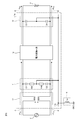
- FIG. 1 is a diagram showing a schematic configuration of a power conversion device according to the first embodiment.
- FIG. 2 is a diagram showing a schematic configuration of a power conversion device according to a comparative example.
- FIG. 3 is a diagram showing an example of conduction noise on the AC side when the Y capacitor is not provided.
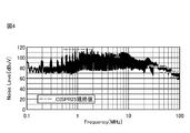
- FIG. 4 is a diagram showing an example of conduction noise on the DC side when the Y capacitor is not provided.
- FIG. 5 is a diagram showing a schematic configuration of the power conversion device according to the second embodiment.
- FIG. 6 is a diagram showing a schematic configuration of the power conversion device according to the third embodiment.
- FIG. 7 is a diagram showing a schematic configuration of the power conversion device according to the fourth embodiment.
- FIG. 1 is a diagram showing a schematic configuration of a power conversion device according to the first embodiment.
- FIG. 2 is a diagram showing a schematic configuration of a power conversion device according to a comparative example.
- FIG. 3 is a diagram showing an example of conduction
- FIG. 8 is a diagram showing a schematic configuration of the power conversion device according to the fifth embodiment.
- FIG. 9 is a diagram showing a schematic configuration of a power conversion device according to a first modification of the fifth embodiment.
- FIG. 10 is a diagram showing a schematic configuration of a power conversion device according to a second modification of the fifth embodiment.
- FIG. 11 is a diagram showing a schematic configuration of a power conversion device according to a third modification of the fifth embodiment.
- FIG. 1 is a diagram showing a schematic configuration of a power conversion device according to the first embodiment.
- the power conversion device 1 for example, an OBC for charging an in-vehicle battery mounted on an EV or PHEV is exemplified.
- the power conversion device 1 converts AC input from an AC power source 2 (for example, a commercial power source such as a charging stand) into DC and supplies it to a load 3 (for example, an in-vehicle battery).
- an AC power source 2 for example, a commercial power source such as a charging stand
- a load 3 for example, an in-vehicle battery
- the power conversion device 1 includes a power conversion circuit 10, a frame ground FG, and a first filter circuit 11 provided between the positive electrode input path A and the negative electrode input path A'of AC. And a second filter circuit 12 provided between the positive electrode output path B and the negative electrode output path B'of the DC.
- the positive electrode path A and the negative electrode path A'of AC are collectively referred to as an "AC line”.
- the positive output path B and the negative output path B'of DC are collectively referred to as a "DC line”.
- the power conversion circuit 10 is composed of, for example, a rectifier circuit, a power factor improving circuit, a DC / DC converter, and the like.
- the power conversion circuit 10 converts the AC input from the AC line into DC and outputs it to the DC line.
- the frame ground FG is, for example, an OBC metal housing.
- the frame ground FG is grounded via the wiring 4.
- the wiring 4 is, for example, a shielded braided wire of a charging cable mounted on an EV or PHEV.
- the first filter circuit 11 is a filter circuit provided in front of the power conversion circuit 10 in order to suppress common mode noise superimposed on the AC line.
- the first filter circuit 11 includes a first capacitor C1 and a first ferrite bead FB1 connected in series between the positive electrode input path A of the AC and the frame ground FG, and the negative electrode input path A'of the AC and the frame ground FG.
- a second capacitor C2 and a second ferrite bead FB2 connected in series with the second capacitor C2 are provided.
- the first capacitor C1 and the second capacitor C2 form a Y capacitor (line bypass capacitor) connected between the AC line and the frame ground FG.
- the common mode noise superimposed on the AC line flows to the frame ground FG via the first filter circuit 11.
- the second filter circuit 12 is a filter circuit provided after the power conversion circuit 10 in order to suppress common mode noise superimposed on the DC line.
- the second filter circuit 12 is connected between the third capacitor C3 connected between the positive output path B of the DC and the frame ground FG, and between the negative output path B'of the DC and the frame ground FG.
- a fourth capacitor C4 is provided.
- the third capacitor C3 and the fourth capacitor C4 form a Y capacitor (line bypass capacitor) connected between the DC line and the frame ground FG.
- the common mode noise superimposed on the DC line flows to the frame ground FG via the second filter circuit 12.
- FIG. 2 is a diagram showing a schematic configuration of a power conversion device according to a comparative example.
- the first filter circuit 111 provided in front of the power conversion circuit 110 is the first with respect to the configuration of the power conversion device 1 according to the first embodiment shown in FIG. It does not have the ferrite beads FB1 and the second ferrite beads FB2.
- FIG. 3 is a diagram showing an example of conduction noise on the AC side when the Y capacitor is not provided.
- the straight line shown in FIG. 3 exemplifies the standard value of the conduction noise of the AC line in CIRPR14.
- the first filter circuit is used so that the conduction noise of the AC line does not exceed the standard value.
- the capacitance values of the first capacitor C1 and the second capacitor C2 constituting the Y capacitor of 111 are set.
- FIG. 4 is a diagram showing an example of conduction noise on the DC side when the Y capacitor is not provided.
- the straight line shown in FIG. 4 exemplifies the standard value of the conduction noise superimposed on the power harness of the in-vehicle electronic device in CISPR25.
- the second filter circuit is used so that the conduction noise of the DC line does not exceed the standard value.
- the capacitance values of the third capacitor C3 and the fourth capacitor C4 constituting the Y capacitor of 112 are set.
- the frame ground FG is grounded by wiring 4 such as a shielded braided wire of a charging cable mounted on an EV or PHEV, for example.
- the wiring 4 contains a parasitic inductance component Lp. This parasitic inductance is characterized by low impedance at low frequencies and high impedance at high frequencies.
- the high frequency component of the AC line common mode noise that has flowed from the first filter circuit 111 to the frame ground FG may not flow to the ground potential GND but may flow into the DC line via the second filter circuit 112.
- the high frequency component of the common mode noise of the DC line flowing from the second filter circuit 112 to the frame ground FG may not flow to the ground potential GND but may flow into the AC line via the first filter circuit 111. ..
- the conduction noise of the AC line shown in FIG. 3 has a high noise level in a low frequency band (for example, 150 kHz or more and 1 MHz or less), and a low noise level in a high frequency band (for example, 30 MHz). Therefore, the Y capacitor is mainly used for noise reduction in the low frequency band.
- the conduction noise of the DC line shown in FIG. 4 has a high noise level in a high frequency band (for example, 30 MHz or more and 108 MHz or less). Therefore, the Y capacitor is mainly used for noise reduction in the high frequency band.
- the high frequency component of the common mode noise of the DC line flowing from the second filter circuit 112 to the frame ground FG flows into the AC line via the first filter circuit 111, so that the high frequency is high.
- the conduction noise of the AC line in the band (for example, 30 MHz) may exceed the standard value.
- the first capacitors C1 and the second capacitors constituting the Y capacitor are used.
- the first ferrite beads FB1 and the second ferrite beads FB2 are connected in series to the capacitor C2, respectively.
- Ferrite beads are characterized by having low impedance in a low frequency band (for example, 150 kHz or more and 1 MHz or less) and high impedance in a high frequency band (for example, 30 MHz or more and 108 MHz or less). As a result, it is possible to suppress the high frequency component of the common mode noise of the DC line flowing into the AC line via the second filter circuit 12, the frame ground FG, and the first filter circuit 11.
- FIG. 5 is a diagram showing a schematic configuration of the power conversion device according to the second embodiment.
- the same components as those in the first embodiment are designated by the same reference numerals, and the description thereof will be omitted.
- the power conversion device 1a according to the second embodiment includes a common mode choke coil 13 between the AC power supply 2 and the first filter circuit 11 for the power conversion device 1 according to the first embodiment.
- FIG. 6 is a diagram showing a schematic configuration of the power conversion device according to the third embodiment.
- the same components as those in the first embodiment or the second embodiment are designated by the same reference numerals, and the description thereof will be omitted.
- the power conversion device 1b according to the third embodiment includes a common mode choke coil 14 between the first filter circuit 11 and the power conversion circuit 10 for the power conversion device 1a according to the second embodiment.
- the common mode choke coil 14 may be provided instead of the common mode choke coil 13 of the second embodiment.
- FIG. 7 is a diagram showing a schematic configuration of the power conversion device according to the fourth embodiment.
- the same components as those in the first embodiment, the second embodiment, or the third embodiment are designated by the same reference numerals, and the description thereof will be omitted.
- the power conversion device 1c according to the fourth embodiment includes a common mode choke coil 15 between the power conversion circuit 10 and the second filter circuit 12 for the power conversion device 1b according to the third embodiment.
- the configuration may not include either or both of the common mode choke coil 13 and the common mode choke coil 14.
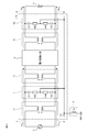
- FIG. 8 is a diagram showing a schematic configuration of the power conversion device according to the fifth embodiment.
- FIG. 9 is a diagram showing a schematic configuration of a power conversion device according to a first modification of the fifth embodiment.
- FIG. 10 is a diagram showing a schematic configuration of a power conversion device according to a second modification of the fifth embodiment.
- FIG. 11 is a diagram showing a schematic configuration of a power conversion device according to a third modification of the fifth embodiment.
- the same components as those in the first embodiment, the second embodiment, the third embodiment, or the fourth embodiment are designated by the same reference numerals, and the description thereof will be omitted.
- the second filter circuit 12a includes a third capacitor C3 and a third ferrite bead FB3 connected in series between the positive electrode output path B of the DC and the frame ground FG, and a DC. It is provided with a fourth capacitor C4 and a fourth ferrite bead FB4 connected in series between the negative electrode output path B'of the above and the frame ground FG. As a result, it is possible to suppress the high frequency component of the common mode noise of the AC line flowing into the DC line via the first filter circuit 11, the frame ground FG, and the second filter circuit 12.
- the common mode choke coil 13 is located between the AC power supply 2 and the first filter circuit 11 with respect to the configuration shown in FIG. It may be configured with.
- the common mode noise superimposed on the AC line can be reduced as compared with the first embodiment, and the conduction noise of the AC line can be further suppressed.
- a common mode choke coil is provided between the first filter circuit 11 and the power conversion circuit 10 with respect to the configuration shown in FIG. A configuration including 14 may be used.
- the common mode noise superimposed on the AC line can be reduced as compared with the second embodiment, and the conduction noise of the AC line can be further suppressed.
- the configuration may include a common mode choke coil 14 instead of the common mode choke coil 13.
- a common mode choke coil is provided between the power conversion circuit 10 and the second filter circuit 12 with respect to the configuration shown in FIG. A configuration including 15 may be used.
- the common mode noise superimposed on the DC line can be reduced as compared with the configurations shown in FIGS. 8, 9 and 10, and the conduction noise of the DC line can be suppressed.
- the configuration may not include either or both of the common mode choke coil 13 and the common mode choke coil 14.
- present disclosure may have the following configuration as described above or in place of the above.
- the power conversion device on one aspect of the present disclosure is a power conversion device that converts AC power input from an AC power supply into DC power, and includes a power conversion circuit and a frame ground grounded via wiring.
- the first filter circuit provided between the positive input path and the negative input path of the AC power, and the second filter provided between the positive output path and the negative output path of the DC power.
- the first filter circuit comprises a circuit, and the first filter circuit includes a first capacitor and a first ferrite bead connected in series between the positive input path and the frame ground, and the negative input path and the frame ground.
- the second filter circuit comprises a second capacitor and a second ferrite bead connected in series between the two, and the second filter circuit includes a third capacitor connected between the positive output path and the frame ground, and the negative electrode.
- a fourth capacitor connected between the sex output path and the frame ground is provided.
- the power conversion device on one aspect of the present disclosure is a power conversion device that converts AC power input from an AC power supply into DC power, and includes a power conversion circuit and a frame ground grounded via wiring.
- the first filter circuit provided between the positive input path and the negative input path of the AC power, and the second filter provided between the positive output path and the negative output path of the DC power.
- the first filter circuit includes a first capacitor and a first ferrite bead connected in series between the positive input path and the frame ground, and the negative input path and the frame ground.
- the second filter circuit comprises a second capacitor and a second ferrite bead connected in series between the two, and the second filter circuit has a third capacitor and a third capacitor connected in series between the positive output path and the frame ground.
- a ferrite bead and a fourth capacitor and a fourth ferrite bead connected in series between the negative output path and the frame ground are provided.
- the common mode noise superimposed on the AC line can be reduced as compared with the above (1) or (2), and the conduction noise of the AC line can be further suppressed.
- the common mode noise in the low frequency band superimposed on the AC line can be reduced as compared with the above (1) or (2), and the conduction noise of the AC line can be further suppressed.
- the common mode noise superimposed on the DC line can be reduced as compared with the above (1) or (2), and the conduction noise of the DC line can be further suppressed.
- Power conversion device 2 AC power supply 3 Load 4 Wiring 10 Power conversion circuit 11 1st filter circuit 12, 12a 2nd filter circuit 100 Power conversion device 110 Power conversion circuit 111 1st filter circuit 112 2nd filter circuit
Landscapes
- Engineering & Computer Science (AREA)
- Power Engineering (AREA)
- Power Conversion In General (AREA)
- Rectifiers (AREA)
- Filters And Equalizers (AREA)
- Inverter Devices (AREA)
Priority Applications (2)
| Application Number | Priority Date | Filing Date | Title |
|---|---|---|---|
| JP2022521863A JPWO2021230137A1 (https=) | 2020-05-15 | 2021-05-06 | |
| JP2024012590A JP7652306B2 (ja) | 2020-05-15 | 2024-01-31 | 車載用電力変換装置 |
Applications Claiming Priority (2)
| Application Number | Priority Date | Filing Date | Title |
|---|---|---|---|
| JP2020086115 | 2020-05-15 | ||
| JP2020-086115 | 2020-05-15 |
Publications (1)
| Publication Number | Publication Date |
|---|---|
| WO2021230137A1 true WO2021230137A1 (ja) | 2021-11-18 |
Family
ID=78525789
Family Applications (1)
| Application Number | Title | Priority Date | Filing Date |
|---|---|---|---|
| PCT/JP2021/017412 Ceased WO2021230137A1 (ja) | 2020-05-15 | 2021-05-06 | 電力変換装置 |
Country Status (2)
| Country | Link |
|---|---|
| JP (2) | JPWO2021230137A1 (https=) |
| WO (1) | WO2021230137A1 (https=) |
Cited By (1)
| Publication number | Priority date | Publication date | Assignee | Title |
|---|---|---|---|---|
| US20230327545A1 (en) * | 2020-12-21 | 2023-10-12 | Murata Manufacturing Co., Ltd. | Power factor correction switching power supply device |
Citations (4)
| Publication number | Priority date | Publication date | Assignee | Title |
|---|---|---|---|---|
| JPH10313571A (ja) * | 1997-05-08 | 1998-11-24 | Matsushita Electric Ind Co Ltd | スイッチング電源装置 |
| JPH11346477A (ja) * | 1998-06-03 | 1999-12-14 | Yaskawa Electric Corp | インバータ装置 |
| JP2008182784A (ja) * | 2007-01-23 | 2008-08-07 | Ntt Advanced Technology Corp | 電源回路 |
| WO2020208825A1 (ja) * | 2019-04-12 | 2020-10-15 | 三菱電機株式会社 | 電力変換装置および空気調和機 |
-
2021
- 2021-05-06 JP JP2022521863A patent/JPWO2021230137A1/ja active Pending
- 2021-05-06 WO PCT/JP2021/017412 patent/WO2021230137A1/ja not_active Ceased
-
2024
- 2024-01-31 JP JP2024012590A patent/JP7652306B2/ja active Active
Patent Citations (4)
| Publication number | Priority date | Publication date | Assignee | Title |
|---|---|---|---|---|
| JPH10313571A (ja) * | 1997-05-08 | 1998-11-24 | Matsushita Electric Ind Co Ltd | スイッチング電源装置 |
| JPH11346477A (ja) * | 1998-06-03 | 1999-12-14 | Yaskawa Electric Corp | インバータ装置 |
| JP2008182784A (ja) * | 2007-01-23 | 2008-08-07 | Ntt Advanced Technology Corp | 電源回路 |
| WO2020208825A1 (ja) * | 2019-04-12 | 2020-10-15 | 三菱電機株式会社 | 電力変換装置および空気調和機 |
Cited By (2)
| Publication number | Priority date | Publication date | Assignee | Title |
|---|---|---|---|---|
| US20230327545A1 (en) * | 2020-12-21 | 2023-10-12 | Murata Manufacturing Co., Ltd. | Power factor correction switching power supply device |
| US12431793B2 (en) * | 2020-12-21 | 2025-09-30 | Murata Manufacturing Co., Ltd. | Power factor correction switching power supply device |
Also Published As
| Publication number | Publication date |
|---|---|
| JP7652306B2 (ja) | 2025-03-27 |
| JPWO2021230137A1 (https=) | 2021-11-18 |
| JP2024036437A (ja) | 2024-03-15 |
Similar Documents
| Publication | Publication Date | Title |
|---|---|---|
| EP3059838B1 (en) | Noise filter | |
| CN103797721B (zh) | 供电系统和连接器 | |
| WO2003098799A1 (en) | Noise suppressing circuit | |
| CN105359377A (zh) | 充电装置及车辆 | |
| CN102386752A (zh) | 噪声滤波器和使用该噪声滤波器的emc滤波器 | |
| US9973042B2 (en) | Power transmission system | |
| JPWO2019130874A1 (ja) | 電源装置 | |
| CN114977774A (zh) | 具有emi抑制的驱动电路及汽车电机驱动系统 | |
| US12291105B2 (en) | Motor vehicle having a DC voltage onboard power supply | |
| JP7652306B2 (ja) | 車載用電力変換装置 | |
| CN106657715B (zh) | 一种车载模拟视频信号抗干扰系统 | |
| US11038415B2 (en) | Power supply device | |
| US20110234337A1 (en) | Filter circuit for differential communication | |
| CN106787670B (zh) | 功率因数改善电路以及应用该电路的车辆充电器 | |
| JP5826024B2 (ja) | ノイズ低減回路 | |
| JP2024535636A (ja) | フィルター・ユニット、フィルター装置及び伝送装置 | |
| JP2005161940A (ja) | 自動車用空調装置 | |
| CN114928241B (zh) | 一种隔离式acdc变换器、充电设备及电源系统 | |
| JP6239468B2 (ja) | 医療装置 | |
| KR20160046416A (ko) | 노이즈 보상 회로 | |
| CN105101770A (zh) | 一种电动车压缩机防电磁干扰系统 | |
| US20250070652A1 (en) | Damping filters for reduced electromagnetic emissions | |
| US11565595B2 (en) | Filter circuit arrangement, an electric vehicle and a method of operating an electric vehicle | |
| CN115411949A (zh) | 变频器及电源系统 | |
| US20250379515A1 (en) | System for an on-board electrical system of a vehicle |
Legal Events
| Date | Code | Title | Description |
|---|---|---|---|
| 121 | Ep: the epo has been informed by wipo that ep was designated in this application |
Ref document number: 21804834 Country of ref document: EP Kind code of ref document: A1 |
|
| ENP | Entry into the national phase |
Ref document number: 2022521863 Country of ref document: JP Kind code of ref document: A |
|
| NENP | Non-entry into the national phase |
Ref country code: DE |
|
| 122 | Ep: pct application non-entry in european phase |
Ref document number: 21804834 Country of ref document: EP Kind code of ref document: A1 |