WO2021192051A1 - Semiconductor storage device - Google Patents
Semiconductor storage device Download PDFInfo
- Publication number
- WO2021192051A1 WO2021192051A1 PCT/JP2020/013071 JP2020013071W WO2021192051A1 WO 2021192051 A1 WO2021192051 A1 WO 2021192051A1 JP 2020013071 W JP2020013071 W JP 2020013071W WO 2021192051 A1 WO2021192051 A1 WO 2021192051A1
- Authority
- WO
- WIPO (PCT)
- Prior art keywords
- layer
- semiconductor
- insulating
- insulating layer
- semiconductor layer
- Prior art date
Links
- 239000004065 semiconductor Substances 0.000 title claims abstract description 252
- 238000003860 storage Methods 0.000 title claims abstract description 89
- 230000015654 memory Effects 0.000 claims description 201
- 238000009413 insulation Methods 0.000 abstract description 3
- 101000739175 Trichosanthes anguina Seed lectin Proteins 0.000 description 26
- 102100035813 E3 ubiquitin-protein ligase CBL Human genes 0.000 description 24
- 238000010586 diagram Methods 0.000 description 23
- 238000004519 manufacturing process Methods 0.000 description 18
- 235000010957 calcium stearoyl-2-lactylate Nutrition 0.000 description 17
- 101150041156 CBL1 gene Proteins 0.000 description 11
- 239000000758 substrate Substances 0.000 description 10
- 230000006870 function Effects 0.000 description 9
- 101150109235 CBL4 gene Proteins 0.000 description 8
- VYPSYNLAJGMNEJ-UHFFFAOYSA-N Silicium dioxide Chemical compound O=[Si]=O VYPSYNLAJGMNEJ-UHFFFAOYSA-N 0.000 description 7
- 229910052814 silicon oxide Inorganic materials 0.000 description 7
- 101000715390 Homo sapiens E3 ubiquitin-protein ligase CBL Proteins 0.000 description 6
- 229910052581 Si3N4 Inorganic materials 0.000 description 6
- 238000000034 method Methods 0.000 description 6
- HQVNEWCFYHHQES-UHFFFAOYSA-N silicon nitride Chemical compound N12[Si]34N5[Si]62N3[Si]51N64 HQVNEWCFYHHQES-UHFFFAOYSA-N 0.000 description 6
- 101150039392 CBL3 gene Proteins 0.000 description 5
- 101150058299 Cblc gene Proteins 0.000 description 5
- 102100035275 E3 ubiquitin-protein ligase CBL-C Human genes 0.000 description 5
- NRTOMJZYCJJWKI-UHFFFAOYSA-N Titanium nitride Chemical compound [Ti]#N NRTOMJZYCJJWKI-UHFFFAOYSA-N 0.000 description 5
- 238000005229 chemical vapour deposition Methods 0.000 description 5
- 230000004048 modification Effects 0.000 description 5
- 238000012986 modification Methods 0.000 description 5
- 229910052710 silicon Inorganic materials 0.000 description 5
- 239000010703 silicon Substances 0.000 description 5
- XUIMIQQOPSSXEZ-UHFFFAOYSA-N Silicon Chemical compound [Si] XUIMIQQOPSSXEZ-UHFFFAOYSA-N 0.000 description 4
- 238000001312 dry etching Methods 0.000 description 4
- 238000005530 etching Methods 0.000 description 4
- 101000741396 Chlamydia muridarum (strain MoPn / Nigg) Probable oxidoreductase TC_0900 Proteins 0.000 description 3
- 101000741399 Chlamydia pneumoniae Probable oxidoreductase CPn_0761/CP_1111/CPj0761/CpB0789 Proteins 0.000 description 3
- 101000741400 Chlamydia trachomatis (strain D/UW-3/Cx) Probable oxidoreductase CT_610 Proteins 0.000 description 3
- 229910004298 SiO 2 Inorganic materials 0.000 description 3
- LPQOADBMXVRBNX-UHFFFAOYSA-N ac1ldcw0 Chemical compound Cl.C1CN(C)CCN1C1=C(F)C=C2C(=O)C(C(O)=O)=CN3CCSC1=C32 LPQOADBMXVRBNX-UHFFFAOYSA-N 0.000 description 3
- 230000000694 effects Effects 0.000 description 3
- 239000011810 insulating material Substances 0.000 description 3
- 229910052751 metal Inorganic materials 0.000 description 3
- 239000002184 metal Substances 0.000 description 3
- 239000000203 mixture Substances 0.000 description 3
- 101150045049 CBL5 gene Proteins 0.000 description 2
- MCMNRKCIXSYSNV-UHFFFAOYSA-N Zirconium dioxide Chemical compound O=[Zr]=O MCMNRKCIXSYSNV-UHFFFAOYSA-N 0.000 description 2
- 239000004020 conductor Substances 0.000 description 2
- 239000012535 impurity Substances 0.000 description 2
- 239000000463 material Substances 0.000 description 2
- 229910044991 metal oxide Inorganic materials 0.000 description 2
- 150000004706 metal oxides Chemical class 0.000 description 2
- 150000004767 nitrides Chemical class 0.000 description 2
- TWNQGVIAIRXVLR-UHFFFAOYSA-N oxo(oxoalumanyloxy)alumane Chemical compound O=[Al]O[Al]=O TWNQGVIAIRXVLR-UHFFFAOYSA-N 0.000 description 2
- 230000000149 penetrating effect Effects 0.000 description 2
- 239000010936 titanium Substances 0.000 description 2
- WFKWXMTUELFFGS-UHFFFAOYSA-N tungsten Chemical compound [W] WFKWXMTUELFFGS-UHFFFAOYSA-N 0.000 description 2
- 229910052721 tungsten Inorganic materials 0.000 description 2
- 239000010937 tungsten Substances 0.000 description 2
- 238000001039 wet etching Methods 0.000 description 2
- 101100186130 Arabidopsis thaliana NAC052 gene Proteins 0.000 description 1
- 101100529509 Arabidopsis thaliana RECQL4A gene Proteins 0.000 description 1
- 101100481702 Arabidopsis thaliana TMK1 gene Proteins 0.000 description 1
- 101100481704 Arabidopsis thaliana TMK3 gene Proteins 0.000 description 1
- 101000578349 Homo sapiens Nucleolar MIF4G domain-containing protein 1 Proteins 0.000 description 1
- 102100027969 Nucleolar MIF4G domain-containing protein 1 Human genes 0.000 description 1
- KJTLSVCANCCWHF-UHFFFAOYSA-N Ruthenium Chemical compound [Ru] KJTLSVCANCCWHF-UHFFFAOYSA-N 0.000 description 1
- 101100203168 Saccharomyces cerevisiae (strain ATCC 204508 / S288c) SGS1 gene Proteins 0.000 description 1
- RTAQQCXQSZGOHL-UHFFFAOYSA-N Titanium Chemical compound [Ti] RTAQQCXQSZGOHL-UHFFFAOYSA-N 0.000 description 1
- 229910052782 aluminium Inorganic materials 0.000 description 1
- XAGFODPZIPBFFR-UHFFFAOYSA-N aluminium Chemical compound [Al] XAGFODPZIPBFFR-UHFFFAOYSA-N 0.000 description 1
- -1 aluminum (Al) Chemical class 0.000 description 1
- 230000004888 barrier function Effects 0.000 description 1
- 239000010419 fine particle Substances 0.000 description 1
- 229910052735 hafnium Inorganic materials 0.000 description 1
- VBJZVLUMGGDVMO-UHFFFAOYSA-N hafnium atom Chemical compound [Hf] VBJZVLUMGGDVMO-UHFFFAOYSA-N 0.000 description 1
- 229910052746 lanthanum Inorganic materials 0.000 description 1
- FZLIPJUXYLNCLC-UHFFFAOYSA-N lanthanum atom Chemical compound [La] FZLIPJUXYLNCLC-UHFFFAOYSA-N 0.000 description 1
- 150000002736 metal compounds Chemical class 0.000 description 1
- 239000007769 metal material Substances 0.000 description 1
- 150000002739 metals Chemical class 0.000 description 1
- 230000003647 oxidation Effects 0.000 description 1
- 238000007254 oxidation reaction Methods 0.000 description 1
- 238000005498 polishing Methods 0.000 description 1
- 229910021420 polycrystalline silicon Inorganic materials 0.000 description 1
- 229920005591 polysilicon Polymers 0.000 description 1
- 229910052707 ruthenium Inorganic materials 0.000 description 1
- 150000003377 silicon compounds Chemical class 0.000 description 1
- 239000000126 substance Substances 0.000 description 1
- MZLGASXMSKOWSE-UHFFFAOYSA-N tantalum nitride Chemical compound [Ta]#N MZLGASXMSKOWSE-UHFFFAOYSA-N 0.000 description 1
- 229910052719 titanium Inorganic materials 0.000 description 1
Images


Classifications
-
- H—ELECTRICITY
- H10—SEMICONDUCTOR DEVICES; ELECTRIC SOLID-STATE DEVICES NOT OTHERWISE PROVIDED FOR
- H10B—ELECTRONIC MEMORY DEVICES
- H10B43/00—EEPROM devices comprising charge-trapping gate insulators
- H10B43/20—EEPROM devices comprising charge-trapping gate insulators characterised by three-dimensional arrangements, e.g. with cells on different height levels
- H10B43/23—EEPROM devices comprising charge-trapping gate insulators characterised by three-dimensional arrangements, e.g. with cells on different height levels with source and drain on different levels, e.g. with sloping channels
- H10B43/27—EEPROM devices comprising charge-trapping gate insulators characterised by three-dimensional arrangements, e.g. with cells on different height levels with source and drain on different levels, e.g. with sloping channels the channels comprising vertical portions, e.g. U-shaped channels
-
- H—ELECTRICITY
- H10—SEMICONDUCTOR DEVICES; ELECTRIC SOLID-STATE DEVICES NOT OTHERWISE PROVIDED FOR
- H10B—ELECTRONIC MEMORY DEVICES
- H10B43/00—EEPROM devices comprising charge-trapping gate insulators
- H10B43/10—EEPROM devices comprising charge-trapping gate insulators characterised by the top-view layout
-
- H—ELECTRICITY
- H01—ELECTRIC ELEMENTS
- H01L—SEMICONDUCTOR DEVICES NOT COVERED BY CLASS H10
- H01L23/00—Details of semiconductor or other solid state devices
- H01L23/52—Arrangements for conducting electric current within the device in operation from one component to another, i.e. interconnections, e.g. wires, lead frames
- H01L23/522—Arrangements for conducting electric current within the device in operation from one component to another, i.e. interconnections, e.g. wires, lead frames including external interconnections consisting of a multilayer structure of conductive and insulating layers inseparably formed on the semiconductor body
- H01L23/5226—Via connections in a multilevel interconnection structure
-
- H—ELECTRICITY
- H01—ELECTRIC ELEMENTS
- H01L—SEMICONDUCTOR DEVICES NOT COVERED BY CLASS H10
- H01L23/00—Details of semiconductor or other solid state devices
- H01L23/52—Arrangements for conducting electric current within the device in operation from one component to another, i.e. interconnections, e.g. wires, lead frames
- H01L23/522—Arrangements for conducting electric current within the device in operation from one component to another, i.e. interconnections, e.g. wires, lead frames including external interconnections consisting of a multilayer structure of conductive and insulating layers inseparably formed on the semiconductor body
- H01L23/528—Geometry or layout of the interconnection structure
- H01L23/5283—Cross-sectional geometry
-
- H—ELECTRICITY
- H01—ELECTRIC ELEMENTS
- H01L—SEMICONDUCTOR DEVICES NOT COVERED BY CLASS H10
- H01L29/00—Semiconductor devices adapted for rectifying, amplifying, oscillating or switching, or capacitors or resistors with at least one potential-jump barrier or surface barrier, e.g. PN junction depletion layer or carrier concentration layer; Details of semiconductor bodies or of electrodes thereof ; Multistep manufacturing processes therefor
- H01L29/66—Types of semiconductor device ; Multistep manufacturing processes therefor
- H01L29/66007—Multistep manufacturing processes
- H01L29/66075—Multistep manufacturing processes of devices having semiconductor bodies comprising group 14 or group 13/15 materials
- H01L29/66227—Multistep manufacturing processes of devices having semiconductor bodies comprising group 14 or group 13/15 materials the devices being controllable only by the electric current supplied or the electric potential applied, to an electrode which does not carry the current to be rectified, amplified or switched, e.g. three-terminal devices
- H01L29/66409—Unipolar field-effect transistors
- H01L29/66477—Unipolar field-effect transistors with an insulated gate, i.e. MISFET
-
- H—ELECTRICITY
- H10—SEMICONDUCTOR DEVICES; ELECTRIC SOLID-STATE DEVICES NOT OTHERWISE PROVIDED FOR
- H10B—ELECTRONIC MEMORY DEVICES
- H10B43/00—EEPROM devices comprising charge-trapping gate insulators
- H10B43/20—EEPROM devices comprising charge-trapping gate insulators characterised by three-dimensional arrangements, e.g. with cells on different height levels
-
- H—ELECTRICITY
- H10—SEMICONDUCTOR DEVICES; ELECTRIC SOLID-STATE DEVICES NOT OTHERWISE PROVIDED FOR
- H10B—ELECTRONIC MEMORY DEVICES
- H10B43/00—EEPROM devices comprising charge-trapping gate insulators
- H10B43/30—EEPROM devices comprising charge-trapping gate insulators characterised by the memory core region
- H10B43/35—EEPROM devices comprising charge-trapping gate insulators characterised by the memory core region with cell select transistors, e.g. NAND
-
- G—PHYSICS
- G11—INFORMATION STORAGE
- G11C—STATIC STORES
- G11C16/00—Erasable programmable read-only memories
- G11C16/02—Erasable programmable read-only memories electrically programmable
- G11C16/04—Erasable programmable read-only memories electrically programmable using variable threshold transistors, e.g. FAMOS
- G11C16/0483—Erasable programmable read-only memories electrically programmable using variable threshold transistors, e.g. FAMOS comprising cells having several storage transistors connected in series
Definitions
- the embodiment relates to a semiconductor storage device.
- a semiconductor storage device in which memory cells are arranged three-dimensionally is known.
- the semiconductor storage device of the embodiment is laminated with the first semiconductor layer extending in the first direction and the first semiconductor layer separated from the first semiconductor layer in the second direction intersecting the first direction.
- a second semiconductor layer extending in the first direction, a first conductive layer intersecting the first semiconductor layer and the second semiconductor layer and extending in the second direction, and the first conductive layer extending in the first direction.
- a first insulating layer provided at a first distance from the conductive layer, intersecting the first semiconductor layer and the second semiconductor layer, and extending in the second direction, and the first insulating layer in the first direction.
- a second conductive layer that is provided at a distance of the first distance, intersects the first semiconductor layer and the second semiconductor layer, and extends in the second direction, and the second conductive layer and the first in the first direction. It is provided at a distance of 1 distance, and includes a third conductive layer that intersects the first semiconductor layer and the second semiconductor layer and extends in the second direction.
- FIG. 1 is a block diagram showing a circuit configuration of the semiconductor storage device of the first embodiment.
- FIG. 2 is a perspective view of the memory cell array according to the first embodiment.
- FIG. 3 is a circuit diagram of the memory cell array in the first embodiment.
- FIG. 4 is a circuit diagram showing a connection between the selection gate line and the global selection gate line in the first embodiment.
- FIG. 5 is a circuit diagram showing the connection between the selection gate line and the global selection gate line in the first embodiment.
- FIG. 6 is a diagram showing a layout configuration of the memory cell array in the first embodiment.
- FIG. 7 is a cross-sectional view of the memory cell array in the first embodiment along the X direction.
- FIG. 8 is an enlarged view of the memory cell area according to the first embodiment.
- FIG. 1 is a block diagram showing a circuit configuration of the semiconductor storage device of the first embodiment.
- FIG. 2 is a perspective view of the memory cell array according to the first embodiment.
- FIG. 3 is a circuit diagram of the
- FIG. 9 is a cross-sectional view taken along line A1-A2 of the memory cell region according to the first embodiment.
- FIG. 10 is a cross-sectional view taken along line B1-B2 of the memory cell region according to the first embodiment.
- FIG. 11 is a diagram showing a manufacturing method in the semiconductor storage device of the first embodiment.
- FIG. 12 is a diagram showing a manufacturing method in the semiconductor storage device of the first embodiment.
- FIG. 13 is a diagram showing a manufacturing method in the semiconductor storage device of the first embodiment.
- FIG. 14 is a diagram showing a manufacturing method in the semiconductor storage device of the first embodiment.
- FIG. 15 is a diagram showing a manufacturing method in the semiconductor storage device of the first embodiment.
- FIG. 16 is a diagram showing a manufacturing method in the semiconductor storage device of the first embodiment.
- FIG. 17 is a diagram showing a manufacturing method in the semiconductor storage device of the first embodiment.
- FIG. 18 is a diagram showing a layout configuration of a semiconductor storage device according to a modification of the first embodiment.
- FIG. 19 is a diagram showing a layout configuration of a memory cell array in the second embodiment.
- FIG. 20 is an enlarged view of the memory cell area in the second embodiment.
- FIG. 21 is a diagram showing a layout configuration of a semiconductor storage device according to a modification of the second embodiment.
- FIG. 1 is an example of a block diagram showing a circuit configuration of a semiconductor storage device.
- FIG. 1 a part of the connection of each block is shown by an arrow line, but the connection between blocks is not limited to this.
- the semiconductor storage device 1 includes an input / output circuit 10, a logic control circuit 11, a status register 12, an address register 13, a command register 14, a sequencer 15, a ready / busy circuit 16, a voltage generation circuit 17, and a memory. It includes a cell array 18, a row decoder 19, a sense amplifier 20, a data register 21, and a column decoder 22.
- the input / output circuit 10 controls the input / output of the signal DQ with the external controller 2.
- the signal DQ includes, for example, data DAT, address ADD, and command CMD.
- the input / output circuit 10 transmits the data DAT received from the controller 2 to the data register 21, the address ADD to the address register 13, and the command CMD to the command register 14. Further, the input / output circuit 10 transmits the status information STS received from the status register 12, the data DAT received from the data register 21, the address ADD received from the address register 13, and the like to the controller 2.
- the logic control circuit 11 receives various control signals from the controller 2.
- the logic control circuit 11 controls the input / output circuit 10 and the sequencer 15 according to the received control signal.
- the status register 12 temporarily holds the status information STS in the write operation, the read operation, and the erase operation, and notifies the controller 2 whether or not these operations are normally completed.
- the address register 13 temporarily holds the received address ADD.
- Address ADD includes row address RADD and column address CADD.
- the address register 13 transfers the low address RADD to the low decoder 19 and transfers the column address CADD to the column decoder 22.
- the command register 14 temporarily stores the received command CMD and transfers it to the sequencer 15.
- the sequencer 15 controls the operation of the entire semiconductor storage device 1. Specifically, the sequencer 15 has, for example, a status register 12, a ready / busy circuit 16, a voltage generation circuit 17, a low decoder 19, a sense amplifier 20, a data register 21, and a column decoder 22 according to the received command CMD. Etc. are controlled, and a write operation, a read operation, an erase operation, and the like are executed.
- the ready / busy circuit 16 transmits a ready / busy signal RBn to the controller 2 according to the operating status of the sequencer 15.
- the voltage generation circuit 17 generates various voltages used in the write operation, the read operation, and the erase operation according to the control of the sequencer 15, and the generated voltages are, for example, the memory cell array 18, the row decoder 19, and the sense amplifier 20. And so on.
- the low decoder 19 and the sense amplifier 20 apply the voltage supplied from the voltage generation circuit 17 to the memory cell transistors in the memory cell array 18.
- the memory cell array 18 includes a plurality of blocks BLK0, BLK1, BLK2, ..., BLKm (m is 0 or more) including a plurality of non-volatile memory cell transistors (hereinafter, also referred to as memory cells) associated with rows and columns. Integer).
- blocks BLK0 to BLKm are not limited, they are referred to as block BLK.
- the block BLK includes a plurality of memory units MU.
- Each of the memory unit MUs includes a plurality of memory groups MG.
- the number of the block BLK in the memory cell array 18, the memory unit MU in the block BLK, and the memory group MG in the memory unit MU is arbitrary. Details of the memory cell array 18 will be described later.
- the low decoder 19 decodes the low address RADD.
- the low decoder 19 applies a control voltage supplied from the voltage generation circuit 17 to the transistors in the memory cell array 18 based on the decoding result.
- the sense amplifier 20 senses the data read from the memory cell array 18 during the read operation. Then, the sense amplifier 20 transmits the read data to the data register 21. Further, the sense amplifier 20 transmits the write data to the memory cell array 18 during the write operation.
- the data register 21 includes a plurality of latch circuits.
- the latch circuit temporarily holds write data or read data.
- the column decoder 22 decodes the column address CADD during, for example, a write operation, a read operation, and an erase operation, and selects a latch circuit in the data register 21 based on the decoding result.
- FIG. 2 is a perspective view of the memory cell array 18.
- a part of the insulating layer between the conductive layers is omitted.
- the memory cell array 18 includes a plurality of semiconductor layers 31, a plurality of word line pillar WLPs, a plurality of word line WLs, a plurality of selection gates SGD and SGS, a plurality of contact plugs CSGD and CSGS, and a plurality of selections.
- the semiconductor layer 31 corresponds to one memory group MG described later, and functions as an active area in which a plurality of memory cell transistors MC and channel layers of the selection transistors ST1 and ST2 are formed.
- the semiconductor layer 31 is stretched in the X direction parallel to the semiconductor substrate, separated in the Z direction perpendicular to the semiconductor substrate, and laminated (via an insulating layer (not shown)). Further, the plurality of semiconductor layers 31 laminated in the Z direction are arranged along the Y direction parallel to the semiconductor substrate and orthogonal to (or intersecting with) the X direction.
- a plurality of word line pillars WLPs extending in the Z direction are arranged along the X direction between the plurality of semiconductor layers 31 arranged in the Y direction.
- the plurality of word line pillar WLPs arranged along the X direction and the plurality of semiconductor layers 31 stacked in the Z direction are alternately arranged along the Y direction.
- a word line WL extending in the Y direction is provided above the word line pillar WLP.
- the word wire pillar WLP includes a contact plug CWL (hereinafter, also referred to as a wiring CWL) electrically connected to the word wire WL provided above, and a block insulating layer provided on the side surface.
- a block insulating layer, a charge storage layer, and a tunnel insulating layer are provided between the contact plug CWL of the word line pillar WLP and the semiconductor layer 31 in each of the plurality of semiconductor layers 31 and a layer at the same height from the semiconductor substrate. ing.
- One memory cell transistor MC is provided at a position where one word line pillar WLP and the semiconductor layer 31 intersect. Therefore, the plurality of memory cell transistors MC are connected in the X direction via the semiconductor layer 31. In other words, the channels of the plurality of memory cell transistors MC are connected in the X direction.
- a contact plug CBL is provided in a region near one end of a plurality of semiconductor layers 31 laminated in the Z direction in the X direction.
- the contact plug CBL penetrates a plurality of semiconductor layers 31 laminated in the Z direction and is connected to the plurality of semiconductor layers 31.
- a plurality of contact plugs CBLs are provided corresponding to the plurality of semiconductor layers 31 arranged along the Y direction.
- a bit wire BL extending in the X direction is provided on each contact plug CBL. The plurality of contact plugs CBL are connected to different bit wire BLs.
- a contact plug CSL is provided in a region near the other end of the plurality of semiconductor layers 31 laminated in the Z direction in the X direction.
- the contact plug CSL penetrates a plurality of semiconductor layers 31 laminated in the Z direction and is connected to the plurality of semiconductor layers 31.
- a plurality of contact plug CSLs are provided corresponding to the plurality of semiconductor layers 31 arranged along the Y direction.
- Source lines SL extending in the Y direction are provided on the plurality of contact plugs CSL.
- a plurality of contact plugs CSLs are commonly connected to the source line SL.
- individual selection gates SGD are provided at one end where the contact plug CBL is arranged via different insulating layers, and the same.
- the selection gate SGD provided in the layer is commonly connected to the selection gate line SGDL extending in the Y direction. Therefore, the semiconductor layer 31 and the selection gate line SGDL are not electrically connected.
- individual selection gate SGS is provided at the other end where the contact plug CSL is arranged via different insulating layers.
- the selective gate SGS provided and provided in the same layer is commonly connected to the selective gate line SGSS extending in the Y direction.
- the semiconductor layer 31 and the selection gate line SGSL are not electrically connected.
- a plurality of selection gate lines SGDL and SGSL corresponding to the semiconductor layers 31 of each layer are laminated on the same layer as the plurality of semiconductor layers 31 laminated in the Z direction, respectively.
- a plurality of global selection gate lines GSGDL are provided along the XY plane below the plurality of semiconductor layers 31 stacked in the Z direction and the plurality of selection gate lines SGDL.
- a contact plug CSGD extending in the Z direction is arranged at the intersection of the selection gate line SGDL and the global selection gate line GSGDL.
- the plurality of contact plugs CSGD are arranged along the Y direction.
- the contact plug CSGD has a connection that is electrically connected to any of the plurality of selective gate lines SGDL. That is, the contact plug CSGD electrically connects one of the global selection gate lines GSGDL and one of the selection gate lines SGDL.
- the connecting portions of the plurality of contact plugs CSGD arranged along the Y direction are connected to the selection gate line SGDL of each layer.
- a plurality of semiconductor layers 31 stacked in the Z direction and a plurality of global selection gate lines GSGSL are provided below the selection gate line SGSL along the XY plane.
- a contact plug CSGS extending in the Z direction is provided at the intersection of the selection gate line SGSL and the global selection gate line GSGSL.
- the plurality of contact plugs CSGS are arranged along the Y direction.
- the contact plug CSGS has a connection that is electrically connected to any of the plurality of selective gate wires SGSL. That is, the contact plug CSGS electrically connects one of the global selection gate lines GSGSL and one of the selection gate lines SGSL.
- a plurality of memory groups MG (semiconductor layer 31) corresponding to one selection gate line SGDL and SGSL and arranged along the Y direction are included in one memory unit MU. Further, a plurality of memory units MUs sharing the word line pillar WLP are included in one block BLK.
- FIG. 3 is a circuit diagram of the memory cell array 18.
- FIG. 4 is a circuit diagram showing a connection between the selection gate line SGDL and the global selection gate line GSGDL.
- FIG. 5 is a circuit diagram showing a connection between the selection gate line SGSL and the global selection gate line GSGSL.
- FIG. 3 shows a plurality of memory groups MG corresponding to a plurality of semiconductor layers 31 stacked in the Z direction and commonly connected to one contact plug CBL.
- the example of FIG. 4 shows a contact plug CSGD and a global selection gate line GSGDL connected to each of a plurality of selection gate lines SGDL stacked in the Z direction.
- the example of FIG. 5 shows a contact plug CSGS and a global selection gate line GSGSL connected to each of a plurality of selection gate lines SGSL stacked in the Z direction.
- the selection gate lines corresponding to the uppermost semiconductor layer 31 are referred to as SGDL1 and SGSL1
- the selection gate lines corresponding to the lowest layer semiconductor layer 31 (memory group MG) are referred to as SGDLk (k). (Integer of 2 or more) and SGSLk.
- the memory cell array 18 includes a plurality of memory groups MG.
- Each of the memory groups MG includes two memory strings MSa and MSb, as well as selection transistors ST1 and ST2.
- the memory strings MSa and MSb are not limited, they are referred to as memory strings MS.
- the memory string MSa includes, for example, four memory cell transistors MCa0 to MCa3.
- the memory string MSb includes, for example, four memory cell transistors MCb0 to MCb3.
- the memory cell transistors MCa0 to MCa3 and MCb0 to MCb3 are not limited, they are referred to as memory cell transistors MC.
- the memory cell transistor MC includes a control gate and a charge storage layer, and holds data non-volatilely.
- the memory cell transistor MC may be an FG (floating gate) type using a conductive layer for the charge storage layer, or a MONOS (metal-oxide) using an insulating layer (or a dielectric layer) for the charge storage layer. -nitride-oxide-silicon) type may be used.
- the number of memory cell transistors MC included in each of the memory string MSs may be 8, 16, 32, 48, 64, 96, 128, etc., and the number is limited. It's not something.
- the current paths of the memory cell transistors MCa0 to MCa3 included in the memory string MSa are connected in series.
- the current paths of the memory cell transistors MCb0 to MCb3 included in the memory string MSb are connected in series.
- the drains of the memory cell transistors MCa0 and MCb0 are commonly connected to the source of the selection transistor ST1.
- the sources of the memory cell transistors MCa3 and MCb3 are commonly connected to the drain of the selection transistor ST2.
- the number of selective transistors ST1 and ST2 included in the memory group MG is arbitrary, and may be one or more for each.
- the gates of the memory cell transistors MC of the plurality of memory groups MG arranged along the Z direction are commonly connected to one word line WL via the contact plug CWL of the word line pillar WLP.
- the gates of a plurality of memory cell transistors MCa0 arranged along the Z direction are commonly connected to the word line WLa0.
- the gates of the memory cell transistors MCa1, MCa2, and MCa3 are connected to the word lines WLa1, WLa2, and WLa3, respectively.
- the gates of the memory cell transistors MCb0 to MCb3 are connected to the word lines WLb0 to WLb3, respectively.
- the drains of the selection transistors ST1 of the plurality of memory groups MG arranged along the Z direction are commonly connected to one bit line BL via the contact plug CBL. Further, the selection gate SGDs of the selection transistors ST1 of the plurality of memory groups MG arranged along the Z direction are connected to different selection gate lines SGDL. Specifically, for example, the selection gate SGD1 of the selection transistor ST1 corresponding to the memory group MG arranged on the uppermost layer is connected to the selection gate line SGDL1. The selection gate SGDk of the selection transistor ST1 corresponding to the memory group MG arranged at the bottom layer is connected to the selection gate line SGDLk.
- the sources of the selection transistors ST2 of the plurality of memory groups MG arranged along the Z direction are commonly connected to one source line SL via the contact plug CSL. Further, the selection gate SGS of the selection transistors ST2 of the plurality of memory groups MG arranged along the Z direction is connected to different selection gate lines SGSL. Specifically, for example, the selection gate SGS1 of the selection transistor ST2 corresponding to the memory group MG arranged on the uppermost layer is connected to the selection gate line SGSL1 and the selection transistor corresponding to the memory group MG arranged on the lowermost layer. The selection gate SGSk of ST2 is connected to the selection gate line SGSLk.
- the connection between the selection gate line SGDL, the contact plug CSGD, and the global selection gate line GSGDL will be described with reference to FIG.
- the contact plug CSGDs corresponding to the plurality of selection gate lines SGDL1 to SGDLk stacked in the Z direction are referred to as CSGD1 to CSGDk, respectively, and the global selection gate lines GSGDL are referred to as GSGDL1 to GSGDLk.
- the selection gate line SGDL1 is connected to the global selection gate line GSGDL1 via the contact plug CSGD1.
- the connection between the selection gate line SGSL, the contact plug CSGS, and the global selection gate line GSGSL will be described with reference to FIG.
- the contact plug CSGS corresponding to each of the plurality of selection gate lines SGSL1 to SGSLk stacked in the Z direction will be referred to as CSGS1 to CSGSk
- the global selection gate lines GSGSL will be referred to as GSGSL1 to GSGSLk.
- the selection gate line SGSL1 is connected to the global selection gate line GSGSL1 via the contact plug CSGS1.
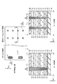
- FIG. 6 is a diagram showing a layout configuration of the memory cell array 18, and is a top view of the uppermost semiconductor layer 31, and the selection gate lines SGDL and SGSL. In the example of FIG. 6, a part of the insulating layer is omitted.
- the memory cell array 18 includes a memory cell area, an SGD area, an SGS area, a selected gate contact area corresponding to the selected gate line SGDL, and a selected gate contact area corresponding to the selected gate line SGSL.
- a memory cell transistor MC is provided in the memory cell area.
- the memory cell transistor MC includes a part of the semiconductor layer 31, a word line pillar WLP, a block insulating layer described later, a charge storage layer, and a tunnel insulating layer.
- the memory cell transistor MC may be simply described as a word line pillar WLP.
- the SGD area is provided adjacent to the memory cell area in the X direction, and functions as a connection area between the semiconductor layer 31 and the contact plug CBL.
- the selection transistor ST1 is provided in the SGD region.
- the SGS region is provided adjacent to the memory cell region in the X direction, and functions as a connection region between the semiconductor layer 31 and the contact plug CSL.
- the selection transistor ST2 is provided in the SGS region.
- the selection gate contact area corresponding to the selection gate line SGDL is provided adjacent to the SGD area in the X direction, and the contact plug CSGD and the selection gate line SGDL are connected.
- the selection gate contact area corresponding to the selection gate line SGSL is provided adjacent to the SGS area in the X direction, and the contact plug CSGS and the selection gate line SGSL are connected to each other.
- the number of memory cell areas, SGD areas, SGS areas, selected gate contact areas corresponding to the selected gate line SGDL, and selected gate contact areas corresponding to the selected gate line SGSL included in the memory cell array 18 is arbitrary.
- a plurality of (12 in the example of FIG. 6) semiconductor layers extending in the X direction (or row direction) are arranged along the Y direction (or column direction).
- Word line pillars WLPs are arranged between the semiconductor layers 31 in the Y direction in a staggered arrangement in the X and Y directions.
- the word line pillars WLP1 and WLP2 are arranged next to each other in the X direction
- the word line pillars WLP3 are arranged between the word line pillars WLP1 and WLP2 in the X direction
- the word line pillars WLP1 and WLP2 are arranged in the Y direction. It is placed in a different position from.
- a plurality of word line pillar WLPs (or memory cell transistors MC) (11 or 12 in the example of FIG. 6) are predetermined between the two semiconductor layers 31 along the X direction. It is arranged at the arrangement pitch P1 of.
- the plurality of word line pillars WLP adjacent to each other in the Y direction are also arranged along the X direction at a predetermined arrangement pitch P1 and are arranged so as to be offset by P1 / 2 in the X direction.
- a plurality of insulating pillars HR1 are arranged at a predetermined distance in the Y direction.
- the insulating pillar HR1 is arranged every other row with respect to the word line pillar WLP arranged in the X direction in the Y direction.
- the insulating pillar HR1 is arranged between two word line pillars WLP arranged in the X direction. In other words, in the word line pillar WLP arranged in the X direction and the Y direction, one row of the word line pillar WLP arranged in the Y direction is replaced with the insulating pillar HR1.
- one row (or a plurality of rows) of word line pillars WLP adjacent to each side in the X direction is a dummy word line pillar with respect to one row of insulating pillars HR1 arranged in the Y direction. It may be set to WDLP.
- the memory cell transistor provided in the dummy word line pillar WDLP is set to a dummy memory cell transistor (hereinafter, also referred to as a dummy cell).
- the number of dummy word line pillars DKLP (that is, dummy memory cell transistors) is arbitrary and may be 0.
- a selective gate SGD is provided on the side surface of the semiconductor layer 31 via a gate oxide layer.
- a plurality of (12 in the example of FIG. 6) contact plugs CBL are connected to a plurality of semiconductor layers 31 arranged along the Y direction.
- the plurality of contact plugs CBLs are provided in a staggered arrangement of four rows (rows) along the Y direction. That is, four contact plugs CBL adjacent to each other in the Y direction are arranged while repeating the four-row pattern in which the four contact plugs CBL are arranged while changing their positions in the X direction.
- the contact plugs CBL1 to CBL4 are arranged while shifting their positions in the X direction in order.
- the contact plug CBL2 adjacent to the contact plug CBL1 is provided at a position different from that of the contact plug CBL1 in the X direction.
- the contact plug CBL3 adjacent to the contact plug CBL2 is provided at a position different from that of the contact plugs CBL1 and CBL2 in the X direction.
- the contact plug CBL4 adjacent to the contact plug CBL3 is provided at a position different from that of the contact plugs CBL1, CBL2, and CBL3 in the X direction.
- the distance between the contact plugs CBL1 and CBL2, the distance between the contact plug CBL2 and the contact plug CBL3, and the distance between the contact plugs CBL3 and CBL4 in the X direction are substantially the same.
- the contact plugs CBL1 to CBL4 are arranged so as to be.
- Such a four-strand staggered arrangement is repeated in the Y direction.
- the contact plug CBL5 adjacent to the contact plug CBL4 in the Y direction is arranged at the same position as the contact plug CBL1 in the X direction.
- the positions of the contact plugs CBL1 to CBL4 in the X direction in the four staggered arrangement are arbitrary.
- the contact plugs CBL1 to CBL4 may not be arranged at the same interval in the X direction, and the order of the contact plugs CBL1 to CBL4 in the X direction may be changed.
- the arrangement of the contact plug CBL is not limited to the quadruple staggered arrangement.
- the plurality of contact plugs CBL may be arranged in a row along the Y direction, or may be arranged in a staggered arrangement of two or more.
- a selective gate SGS is provided on the side surface of the semiconductor layer 31 via a gate oxide layer.
- the two semiconductor layers 31 adjacent to each other along the Y direction are bundled into one and commonly connected to one contact plug CSL.
- two semiconductor layers 31 are commonly connected to one contact plug CSL, but the present invention is not limited to this.
- one contact plug CSL may be provided on one semiconductor layer 31, or three or more semiconductor layers 31 may be bundled and commonly connected to one contact plug CSL.
- a plurality of contact plug CSGDs are provided along the Y direction.
- the plurality of contact plugs CSGD penetrate the plurality of selective gate lines SGDL stacked in the Z direction and are electrically connected to any one of the plurality of selective gate lines SGDL.
- a plurality of insulating pillars HR2 penetrating the plurality of selection gate lines SGDL stacked in the Z direction are provided.
- the arrangement of the insulating pillar HR2 is arbitrary.
- the insulating pillar HR2 is formed by an insulating layer and is not electrically connected to other wiring.
- a plurality of contact plugs CSGS are provided along the Y direction.
- the plurality of contact plugs CSGS penetrate the plurality of selective gate wires SGSL stacked in the Z direction and are electrically connected to any one of the plurality of selective gate wires SGSL.
- a plurality of insulating pillars penetrating the plurality of selection gate lines SGSL stacked in the Z direction are similarly formed in the selection gate contact area corresponding to the selection gate line SGDL.
- HR2 is provided.
- the arrangement of the insulating pillar HR2 is arbitrary.
- the insulating pillar HR2 is formed by an insulating layer and is not electrically connected to other wiring.
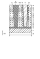
- FIG. 7 is a cross-sectional view of the memory cell array 18 along the X direction. In FIG. 7, a part of the insulating layer is omitted.
- a memory cell array 18 is provided above the semiconductor substrate 50.
- the global selection gate lines GSGDL and GSGSL are provided above the semiconductor substrate 50.
- An insulating layer 52 is provided on the global selection gate lines GSGDL and GSGSL.
- a plurality of laminated semiconductor layers 31 are provided above the insulating layer 52.
- the semiconductor layer 31 in the memory cell region is provided with a contact plug CWL_1 (or a word line pillar WLP) so as to penetrate the semiconductor layer 31.
- a word line WL_1 is provided on the contact plug CWL_1.
- a contact plug CBL_1 is provided in the semiconductor layer 31 in the SGD region so as to penetrate the semiconductor layer 31.
- a contact plug CH_1 is provided on the contact plug CBL_1.
- a contact plug VY is provided on the contact plug CH_1. Further, a bit wire BL extending in the X direction is provided on the contact plug VY.
- a contact plug CSL_1 is provided in the semiconductor layer 31 in the SGS region so as to penetrate the semiconductor layer 31. Further, a source line SL_1 is provided on the contact plug CSL_1.
- the contact plug CSGD in the selected gate contact area is connected to any one of the selected gate lines SGDL, and the bottom surface of the contact plug CSGD is connected to the global selected gate line GSGDL.
- the contact plug CSGS is connected to any one of the selection gate lines SGSL, and the bottom surface of the contact plug CSGS is connected to the global selection gate line GSGSL.
- FIG. 8 is an enlarged view of the region RA in FIG. 7, and shows a layout configuration including the insulating pillar HR1 near the center in the memory cell region. In the example of FIG. 8, a part of the insulating layer is omitted.
- each of the plurality of semiconductor layers 31 extends in the X direction.
- the semiconductor layers 31 are arranged at a predetermined distance along the Y direction.
- the semiconductor layer 31 contains, for example, polysilicon to which impurities have been added.
- a memory trench MT is provided between the two semiconductor layers 31 arranged along the Y direction.
- the memory trench MT is a groove provided to separate the semiconductor layer 31 along the Y direction, and an insulating layer 55 is embedded in the memory trench MT.
- the insulating layer 55 contains, for example, silicon oxide (SiO 2 ).
- An insulating layer 32 is provided between the semiconductor layer 31 and the insulating layer 55.
- the insulating layer 32 functions as an etching stopper when forming the tunnel insulating layer 36 and the charge storage layer 35, which will be described later.
- the insulating layer 32 contains, for example, silicon nitride.
- the word line pillar WLP includes a conductive layer 33 (or contact plug CWL) extending in the Z direction and an insulating layer 34.
- the conductive layer 33 is electrically connected to the upper word line WL and functions as a control gate (or word line) of the memory cell transistor MC.
- a conductive material is used for the conductive layer 33.
- the conductive material may be a metal material, a metal compound, or a semiconductor material to which impurities have been added.
- the conductive layer 33 contains, for example, tungsten (W) and titanium nitride (TiN). TiN is used as a barrier metal when W is formed by CVD (chemical vapor deposition).
- the insulating layer 34 is provided on the side surface of the conductive layer 33 so as to surround the periphery of the conductive layer 33 in the X and Y directions.
- the insulating layer 34 functions as a block insulating layer that prevents the charges accumulated in the charge storage layer 35 from diffusing into the conductive layer 33 (ward wire).
- An insulating material is used for the insulating layer 34.
- the insulating material includes, for example, a high dielectric constant film such as an oxide or a nitride such as aluminum (Al), hafnium (Hf), titanium (Ti), zirconia (Zr) and lanthanum (La), or silicon oxide or silicon.
- a high pressure resistant film such as oxynitride, a mixture thereof, or a laminated film is used.
- a charge storage layer 35 and a tunnel insulating layer 36 are provided between the word line pillar WLP and the semiconductor layer 31 from the word line pillar WLP side. Specifically, the charge storage layer 35 is arranged between the insulating layer 34 and the semiconductor layer 31. Further, a tunnel insulating layer 36 is arranged between the charge storage layer 35 and the semiconductor layer 31.
- the charge storage layer 35 has a function of storing the charge injected from the semiconductor layer 31 in the memory cell transistor MC.
- the charge storage layer 35 may be, for example, an FG type using a conductive layer or a MONOS type using an insulating layer.
- the charge storage layer 35 may also include both an FG type using a conductive layer and a MONOS type using an insulating layer.
- the case where the charge storage layer 35 is of the FG type will be described.
- silicon is used, and metal nitrides such as silicon nitride, tantalum nitride (TaN) and titanium nitride (TiN), metallic silicon compounds such as tungsten (W) and ruthenium (Ru), and metals are used.
- metal nitrides such as silicon nitride, tantalum nitride (TaN) and titanium nitride (TiN), metallic silicon compounds such as tungsten (W) and ruthenium (Ru), and metals are used.
- a mixture such as silicon or an insulating film mixed with fine particles, a laminated film, or the like is used.
- the tunnel insulating layer 36 for example, a mixture of silicon oxide (SiO 2 ), silicon nitride (SiN) or silicon oxynitride (SiON), or a laminated film is used.
- a charge storage layer 35, a tunnel insulating layer 36, and a semiconductor layer 31 are provided at the first and second ends of the word line pillar WLP in the Y direction.
- the block insulating layer 34 is arranged so as to surround the conductive layer 33
- the first charge storage layer 35 is arranged at the first end of the block insulating layer 34 in the Y direction
- the first charge storage layer 35 is arranged at the first end of the block insulating layer 34 in the Y direction
- the first charge storage layer 35 is arranged on the side surface of the first tunnel insulating layer 36 in the Y direction
- the semiconductor layer 31 is arranged on the side surface of the first tunnel insulating layer 36 in the Y direction.
- the conductive layer 33, the block insulating layer 34, the first charge storage layer 35, the first tunnel insulating layer 36, and the semiconductor layer 31 constitute, for example, a memory cell transistor MCa.
- the second charge storage layer 35 is arranged at the second end of the block insulating layer 34 in the Y direction
- the second tunnel insulating layer 36 is arranged on the side surface of the second charge storage layer 35 in the Y direction
- the second is further.
- the semiconductor layer 31 is arranged on the side surface of the tunnel insulating layer 36 in the Y direction.
- the conductive layer 33, the block insulating layer 34, the second charge storage layer 35, the second tunnel insulating layer 36, and the semiconductor layer 31 constitute, for example, a memory cell transistor MCb.
- insulating layers 55 are arranged at both ends of the word line pillar WLP in the X direction.
- the plurality of insulating pillars HR1 are arranged between the two word line pillars WLP in the X direction and arranged in a row in the Y direction.
- a word line pillar WLP, an insulating pillar HR1, and a word line pillar WLP are sequentially arranged between the two semiconductor layers 31 along the X direction at a predetermined arrangement pitch.
- An insulating layer 55 (or a memory trench MT) is arranged between the word line pillar WLP and the insulating pillar HR1.
- the second word line pillar WLP is replaced with the insulating pillar HR1.
- FIG. 9 is a cross-sectional view taken along the line A1-A2 (or the Y direction) of the memory cell area in the memory cell array 18.
- FIG. 10 is a cross-sectional view taken along line B1-B2 (or the X direction) of the memory cell area in the memory cell array 18.
- the insulating layer 51 is provided on the semiconductor substrate 50.
- the insulating layer 51 may include, for example, a transistor (not shown) formed on the semiconductor substrate 50 or a plurality of wiring layers (not shown).
- the insulating layer 51 contains, for example, silicon oxide (SiO 2 ).
- a memory cell array 18 is provided on the insulating layer 51.
- the insulating layer 52 is provided on the insulating layer 51.
- the insulating layer 52 functions as an etching stopper when processing holes used in memory trench MTs, various contact plugs, and the like.
- the insulating layer 52 may be an insulating material capable of obtaining a sufficient etching selectivity with respect to the insulating layer 53 provided on the upper layer.
- the insulating layer 52 contains, for example, a metal oxide such as silicon nitride (SiN) or aluminum oxide (AlO).
- An insulating layer 53 is provided on the insulating layer 52.
- the insulating layer 53 contains, for example, silicon oxide.
- nine semiconductor layers 31 are laminated with the insulating layer 53 interposed therebetween. That is, nine insulating layers 53 and nine semiconductor layers 31 are alternately laminated on the insulating layer 52 to form a laminated body.
- the number of layers of the semiconductor layer 31 is arbitrary.
- An insulating layer 54 is provided on the uppermost semiconductor layer 31.
- the insulating layer 54 contains, for example, silicon oxide.
- the word wire pillar WLP extends in the Z direction so as to intersect with the insulating layer 54, the alternately laminated nine-layer semiconductor layer 31 and the nine-layer insulating layer 53 (that is, the laminated body).
- the word line pillar WLP is formed in the Z direction between the insulating layer 54, the semiconductor layer 31, and the insulating layer 53 and the insulating layer 54, the semiconductor layer 31, and the insulating layer 53 adjacent to each other in the Y direction from above the insulating layer 54. To reach the insulating layer 52.
- the word wire pillar WLP includes a conductive layer 33 and an insulating layer 34 extending in the Z direction.
- the hole AH is formed in the Z direction so as to intersect the insulating layer 54, the semiconductor layer 31, and the insulating layer 53.
- An insulating layer 34 is formed on the side surface and the bottom surface of the hole AH.
- a conductive layer 33 is formed on the side surface of the insulating layer 34 so as to embed the inside of the hole AH.
- a charge storage layer 35 and a tunnel insulating layer 36 are provided between the insulating layer 34 and the semiconductor layer 31 from the insulating layer 34 side. Specifically, a charge storage layer 35 is provided between the insulating layer 34 and the semiconductor layer 31 so as to come into contact with the side surface of the insulating layer 34. Further, a tunnel insulating layer 36 is provided between the charge storage layer 35 and the semiconductor layer 31.
- the insulating pillar HR1 extends in the Z direction so as to intersect the insulating layer 54, the alternately laminated nine-layer semiconductor layer 31 and the nine-layer insulating layer 53.
- the insulating pillar HR1 is formed in the Z direction between the insulating layer 54, the semiconductor layer 31, and the insulating layer 53 and the insulating layer 54, the semiconductor layer 31, and the insulating layer 53 adjacent to each other in the Y direction from above the insulating layer 54. As it passes, it reaches the insulating layer 52.
- the insulating pillar HR1 includes an insulating layer 56 extending in the Z direction. Specifically, the hole H1 is formed in the Z direction so as to intersect the insulating layer 54, the semiconductor layer 31, and the insulating layer 53. Further, the insulating layer 56 is formed so as to embed the inside of the hole H1.
- the memory trench MT is formed in the Z direction between the insulating layer 54, the semiconductor layer 31, and the insulating layer 53 and the insulating layer 54, the semiconductor layer 31, and the insulating layer 53 adjacent to each other in the Y direction from above the insulating layer 54. As it passes, it reaches the insulating layer 52. An insulating layer 55 is provided inside the memory trench MT. Further, an insulating layer 32 is provided between the insulating layer 55 and the semiconductor layer 31.
- 11 to 17 are views showing a method of manufacturing a part of the memory cell area and the selected gate contact area in the memory cell array 18.
- 11 to 17 show the upper surface (upper surface of the semiconductor layer) of the uppermost semiconductor layer 31 in the manufacturing process, the cross section along the A1-A2 line (A1-A2 cross section), and the cross section along the B1-B2 line (the cross section along the B1-B2 line). B1-B2 cross section) are shown respectively.
- the insulating layer 51 and the insulating layer 52 are sequentially laminated on the semiconductor substrate 50.
- nine insulating layers 53 and nine semiconductor layers 31 are alternately laminated on the insulating layer 52.
- the insulating layer 54 is formed on the uppermost semiconductor layer 31.
- insulating pillars HR1 and HR2 are formed in the memory cell area and the selected gate contact area using the same process, respectively. That is, the insulating pillar HR1 is formed in the memory cell region so as to penetrate the insulating layer 54, the insulating layer 53, and the semiconductor layer 31. Using this step for forming the insulating pillar HR1, the insulating pillar HR2 is formed in the selective gate contact region so as to penetrate the insulating layer 54, the insulating layer 53, and the semiconductor layer 31.
- the hole H1 for the insulating pillar HR1 that penetrates the insulating layer 54, the semiconductor layer 31 of the nine layers, and the insulating layer 53 of the nine layers and reaches the insulating layer 52 at the bottom surface is a memory cell area.
- the hole H2 for the insulating pillar HR2 is formed in the selective gate contact region.
- the insulating layer 56 contains, for example, silicon oxide.
- the insulating pillars HR1 and HR2 are formed in the memory cell region and the selective gate contact region by using the same process, but of course, one of the insulating pillars HR1 and the insulating pillars HR2 is formed first, and then the other is formed. You may.
- a memory trench MT is formed in the memory cell area. Specifically, for example, by dry etching, a memory trench MT is formed which penetrates the insulating layer 54, the semiconductor layer 31 of the nine layers, and the insulating layer 53 of the nine layers, and the bottom surface reaches the insulating layer 52.
- the insulating pillar HR1 is left as it is.
- a plurality of laminated semiconductor layers 31 are formed. These laminated semiconductor layers 31 have a high aspect ratio and are easily collapsed (or buckled). In the present embodiment, since the insulating pillar HR1 is arranged between the laminated semiconductor layers 31, it is possible to prevent such collapse of the semiconductor layers 31.
- a part of the semiconductor layer 31 is removed from the side surface in the memory trench MT, and the insulating layer 32 is formed in the removed region. Further, an insulating layer 55 is formed in the memory trench MT.
- a part of the semiconductor layer 31 is etched from the side surface of the opened memory trench MT to form a recess region.
- the insulating layer 32 is formed on the side surface and the bottom surface in the memory trench MT including the recess region and on the insulating layer 54.
- the side surface and the bottom surface in the memory trench MT and the excess insulating layer 32 on the insulating layer 54 are removed by etching back (or dry etching) to leave the insulating layer 32 in the recess region.
- CVD the inside of the memory trench MT is embedded with the insulating layer 55.
- a part of the insulating layer 55 is removed to form a hole AH in the region where the word line pillar WLP should be provided by, for example, dry etching.
- an insulating layer 36 and a charge storage layer 35 are formed on the side surface of the hole AH in the Y direction.
- the insulating layer 32 around the hole AH is removed by wet etching.
- the side surface of the semiconductor layer 31 exposed from the hole AH is oxidized by the oxidation treatment to form the insulating layer 36.
- the charge storage layer 35 is formed on the side surface and the bottom surface in the hole AH and on the insulating layer 54. Further, the side surface and the bottom surface in the hole AH and the excess charge storage layer 35 on the insulating layer 54 are removed by etchback, leaving the charge storage layer 35 on the side surface of the insulating layer 36.
- the insulating layer 34 is formed on the bottom surface and the side surface in the hole AH, and then the conductive layer 33 is formed inside the hole AH.
- the insulating layer 34 is formed on the bottom surface and the side surface in the hole AH by CVD.
- CVD for example, TiN and W as the conductive layer 33 are sequentially formed.
- TiN and W on the insulating layer 54 are removed by, for example, CMP (chemical mechanical polishing).
- one row of insulating pillars HR1 arranged in the Y direction is provided in the memory cell area. Insulation pillars HR1 arranged in the Y direction may be provided in a plurality of rows.
- FIG. 18 is a diagram showing a layout configuration of a semiconductor storage device of a modified example.
- insulating pillars HR1-1 arranged in the Y direction are provided in the memory cell area at a distance D2 from the contact plug CSGD (or contact plug CBL5). Further, the insulating pillar HR1-2 is provided at a distance D2 from the insulating pillar HR1-1.
- the distance D2 is also set between the insulating pillar HR1-2 and the contact plug CSGSD (or contact plug CSL). That is, the distances D2 between the insulating pillar HR1_1 and the contact plug CSGD, between the insulating pillar HR1-1 and the insulating pillar HR1-2, and between the insulating pillar HR1-2 and the contact plug CSGS are set to be substantially equal.
- one row of the word line pillar WLP arranged in the Y direction is replaced with the insulated pillar HR1-1 and the insulated pillar HR_2, respectively.
- the semiconductor storage device has, for example, a laminate in which a plurality of semiconductor layers 31 and a plurality of insulating layers 53 are laminated in the Z direction.
- a memory trench MT is formed in a laminated body in a manufacturing process of a semiconductor storage device, the laminated body is separated by the memory trench MT to become a laminated body having a high aspect ratio, and the laminated body collapses (or buckles) due to stress. In some cases.
- the insulating pillar HR1 extending in the Z direction is provided in the laminated body in which the plurality of semiconductor layers 31 and the plurality of insulating layers 53 in the memory cell region are laminated.
- the insulating pillars HR1 are arranged near the center of the memory cell region in the X direction at a predetermined distance in the Y direction.
- the distance between the insulating pillar HR1 and the contact plug CSGD (or the contact plug CBL) and the distance between the insulating pillar HR1 and the contact plug CSGS (or the contact plug CSL) are set to approximately equal distance D1.
- one word line pillar WLP is replaced with an insulating pillar HR1.
- the insulating pillars HR1-1 and HR1-2 extending in the Z direction are provided in the laminated body in which the plurality of semiconductor layers 31 and the plurality of insulating layers 53 in the memory cell region are laminated.
- the distance D2 between the insulating pillar HR1-1 and the contact plug CSGD, between the insulating pillar HR1-1 and the insulating pillar HR1-2, and between the insulating pillar HR1-2 and the contact plug CSGS is set to be approximately the same.
- the insulating pillars HR1 or the insulating pillars HR1-1 and HR1-2 support the laminated body, and the laminated body in the memory cell area is prevented from collapsing (or buckling). be able to.
- the insulating pillar HR1 in the memory cell region by using the same process as the manufacturing process of the insulating pillar HR2 provided in the selective gate contact region, it is possible to prevent an increase in the number of manufacturing steps, and the manufacturing process. The increase in strike can be suppressed.
- the semiconductor storage device of the second embodiment will be described.
- the second embodiment instead of replacing the word line pillar WLP with the insulating pillar HR1 as in the first embodiment, an example in which the insulated pillar HR1 is provided between two word line pillar WLPs arranged at a predetermined arrangement pitch. Is shown.
- Other circuit configurations, overall configurations, layout configurations, and cross-sectional structures are the same as those in the first embodiment described above.
- the second embodiment mainly describes the differences from the first embodiment.
- FIG. 19 is a diagram showing a layout configuration of the memory cell array 18, and is a top view of the uppermost semiconductor layer 31, and the selection gate lines SGDL and SGSL. In the example of FIG. 19, a part of the insulating layer is omitted.
- the layout configuration of the memory cell array 18 is the same as the configuration shown in FIG. 6 of the first embodiment except for the configuration of the memory cell area.
- FIG. 20 is an enlarged view of the region RA in FIG. 19, and shows a layout configuration including the insulating pillar HR1 near the center in the memory cell region. In the example of FIG. 20, a part of the insulating layer is omitted.
- word line pillar WLPs (or memory cell transistors MC) are arranged along the X direction (or row direction) at a predetermined array pitch P1.
- a plurality of insulating pillars HR1 are arranged at a predetermined distance in the Y direction near the center of the memory cell area in the X direction.
- the insulating pillar HR1 is arranged every other row with respect to the WLP arranged in the X direction in the Y direction.
- the insulating pillar HR1 is arranged between two word line pillar WLPs arranged in the X direction at an arrangement pitch P1. Further, the insulating pillar HR1 is in contact with these two word line pillar WLPs sandwiching the insulating pillar HR1. Further, an insulating layer 55 is arranged between the word line pillars WLP on which the insulating pillar HR1 is not arranged.
- the semiconductor storage device of the modification of the second embodiment will be described.
- the insulating pillar HR1 is provided between two adjacent word line pillar WLPs so as to be in contact with the word line pillar WLPs.
- the insulating pillar HR1 is provided between two adjacent word line pillar WLPs so as not to come into contact with these word line pillar WLPs.
- an insulating pillar HR1 is provided in the vicinity of the SGD area of the memory cell area.
- FIG. 21 is a diagram showing a layout configuration of a semiconductor storage device of a modified example.
- a plurality of (6 or 7 in the example of FIG. 21) word line pillar WLPs are X. They are arranged at a predetermined array pitch P2 along the direction (or row direction). Similarly, the plurality of word line pillars WLPs adjacent to each other in the Y direction are also arranged at a predetermined arrangement pitch P2 along the X direction and are arranged so as to be offset by P2 / 2 in the X direction.
- a plurality of insulating pillars HR1-1 are arranged in the Y direction at a predetermined distance near the center of the memory cell area in the X direction.
- the insulating pillars HR1-1 are arranged every other row with respect to the word line pillars WLP arranged in the X direction in the Y direction. That is, the plurality of insulating pillars HR1-11 are arranged in a row in the Y direction with the word line pillar WLP interposed between the insulating pillars HR1-1 adjacent to each other in the Y direction.
- the insulating pillar HR1-1 is arranged between two word line pillars WLP arranged at an arrangement pitch P2 in the X direction.
- the insulating pillar HR1-1 is not in contact with the two word line pillar WLPs sandwiching the insulating pillar HR1-1.
- a plurality of insulating pillars HR1-2 are arranged at a predetermined distance in the Y direction.
- the plurality of insulating pillars HR1-2 are arranged at one end of the memory cell area in the X direction.
- the insulating pillar HR1-2 is not in contact with the adjacent word line pillar WLP.
- the insulating pillars HR1-1 arranged in the Y direction are provided at a distance of D3 from the contact plug CSGS (or contact plug CSL).
- the insulating pillars HR1-2 arranged in the Y direction are provided at a distance D3 from the insulating pillars HR1-1. That is, the distance D3 between the insulating pillar HR1-1 and the contact plug CSGS and between the insulating pillar HR1-1 and the insulating pillar HR1-2 are set to be substantially equal.
- the insulating pillar HR1_1 is for preventing the collapse of the memory cell area
- the insulating pillar HR1-2 is for preventing the collapse of the SGD area.
- one row (or a plurality of rows) of word line pillars WLP adjacent to the X direction is set as the dummy word line pillar WDLP with respect to the one row of insulated pillars HR1-2 arranged in the Y direction. May be done.
- the memory cell transistor provided in the dummy word line pillar WDLP is set to the dummy memory cell transistor.
- the number of dummy word line pillars DKLP (that is, dummy memory cell transistors) is arbitrary and may be 0.
- the insulating pillar HR1 extending in the Z direction is provided in the laminated body in which the plurality of semiconductor layers 31 and the plurality of insulating layers 53 in the memory cell region are laminated.
- the insulating pillars HR1 are arranged near the center of the memory cell region in the X direction at a predetermined distance in the Y direction.
- the distance between the insulating pillar HR1 and the contact plug CSGD (or the contact plug CBL) and the distance between the insulating pillar HR1 and the contact plug CSGS (or the contact plug CSL) are set to approximately equal distance D1.
- the insulating pillar HR1 is arranged between two adjacent word line pillar WLPs in a plurality of word line pillar WLPs arranged in the X direction at an array pitch P1 so as to be in contact with the two word line pillar WLPs. ing.
- the insulating pillars HR1-1 and HR1-2 extending in the Z direction are provided in the laminated body in which the plurality of semiconductor layers 31 and the plurality of insulating layers 53 in the memory cell region are laminated.
- the insulating pillars HR1-1 are arranged near the center of the memory cell area in the X direction at a predetermined distance in the Y direction.
- the insulating pillar HR1-1 is arranged between two adjacent word line pillar WLPs in a plurality of word line pillar WLPs arranged in the X direction at an array pitch P2 so as not to contact the two word line pillar WLPs. ..
- the insulating pillars HR1-2 are arranged between the memory cell area and the SGD area at a predetermined distance in the Y direction.
- the distance D3 between the insulating pillar HR1_1 and the contact plug CSGS and between the insulating pillar HR1-1 and the insulating pillar HR1-2 are set to be substantially equal.
- the insulating pillars HR1 and HR1-11 support the laminated body, and the laminated body in the memory cell region can be prevented from collapsing (or buckling). Further, in the modified example, the insulating pillar HR1-2 supports the laminated body, and it is possible to prevent the laminated body in the SGD region from collapsing.
- the insulated pillars HR1 or the insulated pillars HR1-1 and HR1-2 are arranged between two adjacent word line pillars WLPs, so that the memory in the memory cell area is stored. It does not reduce the occupancy of the cell transistor MC.
- the insulating pillars HR1 or the insulating pillars HR1-1 and HR1-2 in the memory cell region by using the same process as the manufacturing process of the insulating pillar HR2 provided in the selection gate contact region. , It is possible to prevent an increase in the number of manufacturing processes and suppress an increase in manufacturing work strikes.
- the NAND flash memory has been described as an example as the semiconductor storage device, but the present invention is not limited to the NAND flash memory, and can be applied to other semiconductor memories in general, and various types other than the semiconductor memory. Applicable to storage devices.
Abstract
A semiconductor storage device that, according to the embodiments, comprises a first semiconductor layer that extends in a first direction, a second semiconductor layer that extends in the first direction and is provided so as to be separated from the first semiconductor layer in a second direction that intersects the first direction, a first conduction layer that extends in the second direction and intersects the first semiconductor layer and the second semiconductor layer, a first insulation layer that extends in the second direction, intersects the first semiconductor layer and the second semiconductor layer, and is provided at a first distance from the first conduction layer in the first direction, a second conduction layer that extends in the second direction, intersects the first semiconductor layer and the second semiconductor layer, and is provided at the first distance from the first insulation layer in the first direction, and a third conduction layer that extends in the second direction, intersects the first semiconductor layer and the second semiconductor layer, and is provided at the first distance from the second conduction layer in the first direction.
Description
実施形態は、半導体記憶装置に関する。
The embodiment relates to a semiconductor storage device.
メモリセルが三次元に配列された半導体記憶装置が知られている。
A semiconductor storage device in which memory cells are arranged three-dimensionally is known.
構造倒壊を低減することが可能な半導体記憶装置を提供する。
Provide a semiconductor storage device capable of reducing structural collapse.
実施形態の半導体記憶装置は、実施形態の半導体記憶装置は、第1方向に延伸する第1半導体層と、前記第1方向と交差する第2方向に前記第1半導体層と離隔して積層され、前記第1方向に延伸する第2半導体層と、前記第1半導体層及び前記第2半導体層と交差し、前記第2方向に延伸する第1導電層と、前記第1方向に前記第1導電層と第1距離離れて設けられ、前記第1半導体層及び前記第2半導体層と交差し、前記第2方向に延伸する第1絶縁層と、前記第1方向に前記第1絶縁層と前記第1距離離れて設けられ、前記第1半導体層及び前記第2半導体層と交差し、前記第2方向に延伸する第2導電層と、前記第1方向に前記第2導電層と前記第1距離離れて設けられ、前記第1半導体層及び前記第2半導体層と交差し、前記第2方向に延伸する第3導電層とを具備する。
In the semiconductor storage device of the embodiment, the semiconductor storage device of the embodiment is laminated with the first semiconductor layer extending in the first direction and the first semiconductor layer separated from the first semiconductor layer in the second direction intersecting the first direction. A second semiconductor layer extending in the first direction, a first conductive layer intersecting the first semiconductor layer and the second semiconductor layer and extending in the second direction, and the first conductive layer extending in the first direction. A first insulating layer provided at a first distance from the conductive layer, intersecting the first semiconductor layer and the second semiconductor layer, and extending in the second direction, and the first insulating layer in the first direction. A second conductive layer that is provided at a distance of the first distance, intersects the first semiconductor layer and the second semiconductor layer, and extends in the second direction, and the second conductive layer and the first in the first direction. It is provided at a distance of 1 distance, and includes a third conductive layer that intersects the first semiconductor layer and the second semiconductor layer and extends in the second direction.
以下に、図面を参照して実施形態について説明する。なお、以下の説明において、略同一の機能及び構成を有する構成要素については、共通する参照符号を付す。また、以下に示す各実施形態は、この実施形態の技術的思想を具体化するための装置や方法を例示するものであって、実施形態の技術的思想は、構成部品の材質、形状、構造、配置等を下記のものに特定するものでない。実施形態の技術的思想は、特許請求の範囲において、種々の変更を加えることができる。また、実施形態の半導体記憶装置として、メモリセルトランジスタが半導体基板の上方に三次元に積層された三次元積層型NAND型フラッシュメモリを例に挙げて説明する。
Hereinafter, embodiments will be described with reference to the drawings. In the following description, components having substantially the same function and configuration are designated by a common reference numeral. In addition, each of the embodiments shown below exemplifies devices and methods for embodying the technical idea of this embodiment, and the technical idea of the embodiment is the material, shape, and structure of the component parts. , Arrangement, etc. are not specified as the following. The technical idea of the embodiment can be modified in various ways within the scope of the claims. Further, as the semiconductor storage device of the embodiment, a three-dimensional stacked NAND flash memory in which memory cell transistors are three-dimensionally stacked on a semiconductor substrate will be described as an example.
1.第1実施形態
以下に、第1実施形態の半導体記憶装置について説明する。 1. 1. First Embodiment The semiconductor storage device of the first embodiment will be described below.
以下に、第1実施形態の半導体記憶装置について説明する。 1. 1. First Embodiment The semiconductor storage device of the first embodiment will be described below.
1.1 半導体記憶装置の構成
1.1.1 半導体記憶装置の回路構成
まず、図1を用いて、半導体記憶装置の回路構成について説明する。図1は、半導体記憶装置の回路構成を示すブロック図の一例である。なお、図1では、各ブロックの接続の一部を矢印線により示しているが、ブロック間の接続はこれに限定されない。 1.1 Configuration of semiconductor storage device 1.1.1 Circuit configuration of semiconductor storage device First, the circuit configuration of the semiconductor storage device will be described with reference to FIG. FIG. 1 is an example of a block diagram showing a circuit configuration of a semiconductor storage device. In FIG. 1, a part of the connection of each block is shown by an arrow line, but the connection between blocks is not limited to this.
図1に示すように、半導体記憶装置1は、入出力回路10、ロジック制御回路11、ステータスレジスタ12、アドレスレジスタ13、コマンドレジスタ14、シーケンサ15、レディ/ビジー回路16、電圧発生回路17、メモリセルアレイ18、ロウデコーダ19、センスアンプ20、データレジスタ21、及びカラムデコーダ22を含む。
As shown in FIG. 1, the semiconductor storage device 1 includes an input / output circuit 10, a logic control circuit 11, a status register 12, an address register 13, a command register 14, a sequencer 15, a ready / busy circuit 16, a voltage generation circuit 17, and a memory. It includes a cell array 18, a row decoder 19, a sense amplifier 20, a data register 21, and a column decoder 22.
入出力回路10は、外部のコントローラ2との間において信号DQの入出力を制御する。信号DQは、例えばデータDAT、アドレスADD、及びコマンドCMDを含む。具体的には、入出力回路10は、コントローラ2から受信したデータDATをデータレジスタ21に送信し、またアドレスADDをアドレスレジスタ13に送信し、コマンドCMDをコマンドレジスタ14に送信する。また、入出力回路10は、ステータスレジスタ12から受信したステータス情報STS、データレジスタ21から受信したデータDAT、及びアドレスレジスタ13から受信したアドレスADD等を、コントローラ2に送信する。
The input / output circuit 10 controls the input / output of the signal DQ with the external controller 2. The signal DQ includes, for example, data DAT, address ADD, and command CMD. Specifically, the input / output circuit 10 transmits the data DAT received from the controller 2 to the data register 21, the address ADD to the address register 13, and the command CMD to the command register 14. Further, the input / output circuit 10 transmits the status information STS received from the status register 12, the data DAT received from the data register 21, the address ADD received from the address register 13, and the like to the controller 2.
ロジック制御回路11は、コントローラ2から各種制御信号を受信する。ロジック制御回路11は、受信した制御信号に応じて、入出力回路10及びシーケンサ15を制御する。
The logic control circuit 11 receives various control signals from the controller 2. The logic control circuit 11 controls the input / output circuit 10 and the sequencer 15 according to the received control signal.
ステータスレジスタ12は、例えば、書き込み動作、読み出し動作、及び消去動作におけるステータス情報STSを一時的に保持し、コントローラ2にこれらの動作が正常に終了したか否かを通知する。
The status register 12 temporarily holds the status information STS in the write operation, the read operation, and the erase operation, and notifies the controller 2 whether or not these operations are normally completed.
アドレスレジスタ13は、受信したアドレスADDを一時的に保持する。アドレスADDは、ロウアドレスRADD及びカラムアドレスCADDを含む。アドレスレジスタ13は、ロウアドレスRADDをロウデコーダ19へ転送し、カラムアドレスCADDをカラムデコーダ22に転送する。
The address register 13 temporarily holds the received address ADD. Address ADD includes row address RADD and column address CADD. The address register 13 transfers the low address RADD to the low decoder 19 and transfers the column address CADD to the column decoder 22.
コマンドレジスタ14は、受信したコマンドCMDを一時的に保存し、シーケンサ15に転送する。
The command register 14 temporarily stores the received command CMD and transfers it to the sequencer 15.
シーケンサ15は、半導体記憶装置1全体の動作を制御する。具体的には、シーケンサ15は、受信したコマンドCMDに応じて、例えば、ステータスレジスタ12、レディ/ビジー回路16、電圧発生回路17、ロウデコーダ19、センスアンプ20、データレジスタ21、及びカラムデコーダ22等を制御し、書き込み動作、読み出し動作、及び消去動作等を実行する。
The sequencer 15 controls the operation of the entire semiconductor storage device 1. Specifically, the sequencer 15 has, for example, a status register 12, a ready / busy circuit 16, a voltage generation circuit 17, a low decoder 19, a sense amplifier 20, a data register 21, and a column decoder 22 according to the received command CMD. Etc. are controlled, and a write operation, a read operation, an erase operation, and the like are executed.
レディ/ビジー回路16は、シーケンサ15の動作状況に応じて、レディ/ビジー信号RBnをコントローラ2に送信する。
The ready / busy circuit 16 transmits a ready / busy signal RBn to the controller 2 according to the operating status of the sequencer 15.
電圧発生回路17は、シーケンサ15の制御に応じて、書き込み動作、読み出し動作、及び消去動作で用いられる各種電圧を発生し、発生した電圧を、例えばメモリセルアレイ18、ロウデコーダ19、及びセンスアンプ20等に供給する。ロウデコーダ19及びセンスアンプ20は、電圧発生回路17より供給された電圧をメモリセルアレイ18内のメモリセルトランジスタに印加する。
The voltage generation circuit 17 generates various voltages used in the write operation, the read operation, and the erase operation according to the control of the sequencer 15, and the generated voltages are, for example, the memory cell array 18, the row decoder 19, and the sense amplifier 20. And so on. The low decoder 19 and the sense amplifier 20 apply the voltage supplied from the voltage generation circuit 17 to the memory cell transistors in the memory cell array 18.
メモリセルアレイ18は、ロウ及びカラムに対応付けられた複数の不揮発性のメモリセルトランジスタ(以下、メモリセルとも表記する)を含む複数のブロックBLK0、BLK1、BLK2、…、BLKm(mは0以上の整数)を備えている。以下、ブロックBLK0~BLKmを限定しない場合は、ブロックBLKと表記する。
The memory cell array 18 includes a plurality of blocks BLK0, BLK1, BLK2, ..., BLKm (m is 0 or more) including a plurality of non-volatile memory cell transistors (hereinafter, also referred to as memory cells) associated with rows and columns. Integer). Hereinafter, when the blocks BLK0 to BLKm are not limited, they are referred to as block BLK.
ブロックBLKは、複数のメモリユニットMUを含む。そしてメモリユニットMUの各々は、複数のメモリグループMGを含む。なお、メモリセルアレイ18内のブロックBLK、ブロックBLK内のメモリユニットMU、及びメモリユニットMU内のメモリグループMGの個数は任意である。メモリセルアレイ18の詳細については後述する。
The block BLK includes a plurality of memory units MU. Each of the memory unit MUs includes a plurality of memory groups MG. The number of the block BLK in the memory cell array 18, the memory unit MU in the block BLK, and the memory group MG in the memory unit MU is arbitrary. Details of the memory cell array 18 will be described later.
ロウデコーダ19は、ロウアドレスRADDをデコードする。ロウデコーダ19は、デコード結果に基づいて、メモリセルアレイ18内のトランジスタに電圧発生回路17より供給された制御用の電圧を印加する。
The low decoder 19 decodes the low address RADD. The low decoder 19 applies a control voltage supplied from the voltage generation circuit 17 to the transistors in the memory cell array 18 based on the decoding result.
センスアンプ20は、読み出し動作時に、メモリセルアレイ18から読み出されたデータをセンスする。そして、センスアンプ20は、読み出しデータをデータレジスタ21に送信する。また、センスアンプ20は、書き込み動作時に、書き込みデータをメモリセルアレイ18に送信する。
The sense amplifier 20 senses the data read from the memory cell array 18 during the read operation. Then, the sense amplifier 20 transmits the read data to the data register 21. Further, the sense amplifier 20 transmits the write data to the memory cell array 18 during the write operation.
データレジスタ21は、複数のラッチ回路を備える。ラッチ回路は、書き込みデータまたは読み出しデータを一時的に保持する。
The data register 21 includes a plurality of latch circuits. The latch circuit temporarily holds write data or read data.
カラムデコーダ22は、例えば書き込み動作、読み出し動作、及び消去動作の際、カラムアドレスCADDをデコードし、デコード結果に基づいてデータレジスタ21内のラッチ回路を選択する。
The column decoder 22 decodes the column address CADD during, for example, a write operation, a read operation, and an erase operation, and selects a latch circuit in the data register 21 based on the decoding result.
1.1.2 メモリセルアレイの全体構成
次に、図2を用いて、メモリセルアレイ18の全体構成について説明する。図2は、メモリセルアレイ18の斜視図である。なお、図2の例では、導電層間の絶縁層の一部が省略されている。 1.1.2 Overall configuration of the memory cell array Next, the overall configuration of thememory cell array 18 will be described with reference to FIG. FIG. 2 is a perspective view of the memory cell array 18. In the example of FIG. 2, a part of the insulating layer between the conductive layers is omitted.
次に、図2を用いて、メモリセルアレイ18の全体構成について説明する。図2は、メモリセルアレイ18の斜視図である。なお、図2の例では、導電層間の絶縁層の一部が省略されている。 1.1.2 Overall configuration of the memory cell array Next, the overall configuration of the
図2に示すように、メモリセルアレイ18は、複数の半導体層31、複数のワード線ピラーWLP、複数のワード線WL、複数の選択ゲートSGD及びSGS、複数のコンタクトプラグCSGD及びCSGS、複数の選択ゲート線SGDL及びSGSL、複数のグローバル選択ゲート線GSGDL、複数のコンタクトプラグCBL、複数のビット線BL、複数のコンタクトプラグCSL、及びソース線SLを含む。
As shown in FIG. 2, the memory cell array 18 includes a plurality of semiconductor layers 31, a plurality of word line pillar WLPs, a plurality of word line WLs, a plurality of selection gates SGD and SGS, a plurality of contact plugs CSGD and CSGS, and a plurality of selections. Includes gate lines SGDL and SGSL, multiple global selection gate lines GSGDL, multiple contact plugs CBL, multiple bit lines BL, multiple contact plugs CSL, and source line SL.
半導体層31は、後述する1つのメモリグループMGに対応し、複数のメモリセルトランジスタMC、選択トランジスタST1及びST2のチャネル層が形成されるアクティブエリアとして機能する。半導体層31は、半導体基板に平行なX方向に延伸し、半導体基板に垂直なZ方向に離隔して(図示せぬ絶縁層を介して)積層されている。さらに、Z方向に積層された複数の半導体層31は、半導体基板に平行で且つX方向に直交(または、交差)するY方向に沿って配列されている。
The semiconductor layer 31 corresponds to one memory group MG described later, and functions as an active area in which a plurality of memory cell transistors MC and channel layers of the selection transistors ST1 and ST2 are formed. The semiconductor layer 31 is stretched in the X direction parallel to the semiconductor substrate, separated in the Z direction perpendicular to the semiconductor substrate, and laminated (via an insulating layer (not shown)). Further, the plurality of semiconductor layers 31 laminated in the Z direction are arranged along the Y direction parallel to the semiconductor substrate and orthogonal to (or intersecting with) the X direction.
Y方向に配置された複数の半導体層31の間には、Z方向に延伸する複数のワード線ピラーWLPがX方向に沿って配列されている。換言すれば、X方向に沿って配列された複数のワード線ピラーWLPと、Z方向に積層された複数の半導体層31とが、Y方向に沿って交互に配列されている。ワード線ピラーWLPの上方には、Y方向に延伸するワード線WLが設けられている。ワード線ピラーWLPは、上方に設けられたワード線WLに電気的に接続されるコンタクトプラグCWL(以下、配線CWLとも表記する)と、側面に設けられたブロック絶縁層とを含む。複数の半導体層31の各々と半導体基板から同一高さの層において、ワード線ピラーWLPのコンタクトプラグCWLと半導体層31との間には、ブロック絶縁層、電荷蓄積層及びトンネル絶縁層が設けられている。
A plurality of word line pillars WLPs extending in the Z direction are arranged along the X direction between the plurality of semiconductor layers 31 arranged in the Y direction. In other words, the plurality of word line pillar WLPs arranged along the X direction and the plurality of semiconductor layers 31 stacked in the Z direction are alternately arranged along the Y direction. Above the word line pillar WLP, a word line WL extending in the Y direction is provided. The word wire pillar WLP includes a contact plug CWL (hereinafter, also referred to as a wiring CWL) electrically connected to the word wire WL provided above, and a block insulating layer provided on the side surface. A block insulating layer, a charge storage layer, and a tunnel insulating layer are provided between the contact plug CWL of the word line pillar WLP and the semiconductor layer 31 in each of the plurality of semiconductor layers 31 and a layer at the same height from the semiconductor substrate. ing.
1つのワード線ピラーWLPと半導体層31とが交差する位置に、1つのメモリセルトランジスタMCが設けられる。従って、複数のメモリセルトランジスタMCが、半導体層31を介して、X方向に接続される。換言すれば、複数のメモリセルトランジスタMCのチャネルが、X方向に接続される。
One memory cell transistor MC is provided at a position where one word line pillar WLP and the semiconductor layer 31 intersect. Therefore, the plurality of memory cell transistors MC are connected in the X direction via the semiconductor layer 31. In other words, the channels of the plurality of memory cell transistors MC are connected in the X direction.
Z方向に積層された複数の半導体層31のX方向における一端の近傍領域には、コンタクトプラグCBLが設けられている。コンタクトプラグCBLは、Z方向に積層された複数の半導体層31を貫通し、これら複数の半導体層31に接続される。Y方向に沿って配列された複数の半導体層31に対応して、複数のコンタクトプラグCBLが、設けられている。各コンタクトプラグCBL上には、X方向に延伸するビット線BLが設けられる。複数のコンタクトプラグCBLは、それぞれ異なるビット線BLに接続される。
A contact plug CBL is provided in a region near one end of a plurality of semiconductor layers 31 laminated in the Z direction in the X direction. The contact plug CBL penetrates a plurality of semiconductor layers 31 laminated in the Z direction and is connected to the plurality of semiconductor layers 31. A plurality of contact plugs CBLs are provided corresponding to the plurality of semiconductor layers 31 arranged along the Y direction. A bit wire BL extending in the X direction is provided on each contact plug CBL. The plurality of contact plugs CBL are connected to different bit wire BLs.
Z方向に積層された複数の半導体層31のX方向における他端の近傍領域には、コンタクトプラグCSLが設けられている。コンタクトプラグCSLは、Z方向に積層された複数の半導体層31を貫通し、これら複数の半導体層31に接続される。Y方向に沿って配列された複数の半導体層31に対応して、複数のコンタクトプラグCSLが設けられている。複数のコンタクトプラグCSL上には、Y方向に延伸するソース線SLが設けられる。複数のコンタクトプラグCSLは、ソース線SLに共通に接続される。
A contact plug CSL is provided in a region near the other end of the plurality of semiconductor layers 31 laminated in the Z direction in the X direction. The contact plug CSL penetrates a plurality of semiconductor layers 31 laminated in the Z direction and is connected to the plurality of semiconductor layers 31. A plurality of contact plug CSLs are provided corresponding to the plurality of semiconductor layers 31 arranged along the Y direction. Source lines SL extending in the Y direction are provided on the plurality of contact plugs CSL. A plurality of contact plugs CSLs are commonly connected to the source line SL.
Y方向に沿って1つの層に配置された複数の半導体層31のX方向において、コンタクトプラグCBLが配置された一端には、それぞれ異なる絶縁層を介して個別の選択ゲートSGDが設けられ、同じ層に設けられた選択ゲートSGDは、Y方向に延伸する選択ゲート線SGDLに共通に接続される。よって、半導体層31と選択ゲート線SGDLとは電気的に接続されていない。同様に、Y方向に沿って1つの層に配置された複数の半導体層31のX方向において、コンタクトプラグCSLが配置された他端には、それぞれ異なる絶縁層を介して個別の選択ゲートSGSが設けられ、同じ層に設けられた選択ゲートSGSは、Y方向に延伸する選択ゲート線SGSLに共通に接続される。よって、半導体層31と選択ゲート線SGSLとは電気的に接続されていない。Z方向に積層された複数の半導体層31と同層に、それぞれの層の半導体層31に対応する複数の選択ゲート線SGDL及びSGSLが、それぞれ積層される。
In the X direction of the plurality of semiconductor layers 31 arranged in one layer along the Y direction, individual selection gates SGD are provided at one end where the contact plug CBL is arranged via different insulating layers, and the same. The selection gate SGD provided in the layer is commonly connected to the selection gate line SGDL extending in the Y direction. Therefore, the semiconductor layer 31 and the selection gate line SGDL are not electrically connected. Similarly, in the X direction of the plurality of semiconductor layers 31 arranged in one layer along the Y direction, individual selection gate SGS is provided at the other end where the contact plug CSL is arranged via different insulating layers. The selective gate SGS provided and provided in the same layer is commonly connected to the selective gate line SGSS extending in the Y direction. Therefore, the semiconductor layer 31 and the selection gate line SGSL are not electrically connected. A plurality of selection gate lines SGDL and SGSL corresponding to the semiconductor layers 31 of each layer are laminated on the same layer as the plurality of semiconductor layers 31 laminated in the Z direction, respectively.
Z方向に積層された複数の半導体層31と、複数の選択ゲート線SGDLの下方には、XY平面に沿って、複数のグローバル選択ゲート線GSGDLが設けられている。
A plurality of global selection gate lines GSGDL are provided along the XY plane below the plurality of semiconductor layers 31 stacked in the Z direction and the plurality of selection gate lines SGDL.
選択ゲート線SGDLとグローバル選択ゲート線GSGDLとの交点には、Z方向に延伸するコンタクトプラグCSGDが配置されている。複数のコンタクトプラグCSGDは、Y方向に沿って配列されている。コンタクトプラグCSGDは、複数の選択ゲート線SGDLのいずれかと電気的に接続される接続部を有している。すなわち、コンタクトプラグCSGDは、いずれかのグローバル選択ゲート線GSGDLといずれかの選択ゲート線SGDLとを電気的に接続する。図2の例では、Y方向に沿って配列された複数のコンタクトプラグCSGDの接続部が、各層の選択ゲート線SGDLと接続されている。
A contact plug CSGD extending in the Z direction is arranged at the intersection of the selection gate line SGDL and the global selection gate line GSGDL. The plurality of contact plugs CSGD are arranged along the Y direction. The contact plug CSGD has a connection that is electrically connected to any of the plurality of selective gate lines SGDL. That is, the contact plug CSGD electrically connects one of the global selection gate lines GSGDL and one of the selection gate lines SGDL. In the example of FIG. 2, the connecting portions of the plurality of contact plugs CSGD arranged along the Y direction are connected to the selection gate line SGDL of each layer.
Z方向に積層された複数の半導体層31と、選択ゲート線SGSLの下方には、XY平面に沿って、複数のグローバル選択ゲート線GSGSL(不図示)が設けられている。
A plurality of semiconductor layers 31 stacked in the Z direction and a plurality of global selection gate lines GSGSL (not shown) are provided below the selection gate line SGSL along the XY plane.
選択ゲート線SGSLとグローバル選択ゲート線GSGSLとの交点には、Z方向に延伸するコンタクトプラグCSGSが設けられている。複数のコンタクトプラグCSGSは、Y方向に沿って配列されている。コンタクトプラグCSGSは、複数の選択ゲート線SGSLのいずれかと電気的に接続される接続部を有している。すなわち、コンタクトプラグCSGSは、いずれかのグローバル選択ゲート線GSGSLといずれかの選択ゲート線SGSLとを電気的に接続する。
A contact plug CSGS extending in the Z direction is provided at the intersection of the selection gate line SGSL and the global selection gate line GSGSL. The plurality of contact plugs CSGS are arranged along the Y direction. The contact plug CSGS has a connection that is electrically connected to any of the plurality of selective gate wires SGSL. That is, the contact plug CSGS electrically connects one of the global selection gate lines GSGSL and one of the selection gate lines SGSL.
1つの選択ゲート線SGDL及びSGSLに対応し、Y方向に沿って配置された複数のメモリグループMG(半導体層31)が1つのメモリユニットMUに含まれる。また、ワード線ピラーWLPを共有する複数のメモリユニットMUが1つのブロックBLKに含まれる。
A plurality of memory groups MG (semiconductor layer 31) corresponding to one selection gate line SGDL and SGSL and arranged along the Y direction are included in one memory unit MU. Further, a plurality of memory units MUs sharing the word line pillar WLP are included in one block BLK.
1.1.3 メモリセルアレイの回路構成
次に、図3~図5を用いて、メモリセルアレイ18の回路構成について説明する。図3は、メモリセルアレイ18の回路図である。図4は、選択ゲート線SGDLとグローバル選択ゲート線GSGDLとの接続を示す回路図である。図5は、選択ゲート線SGSLとグローバル選択ゲート線GSGSLとの接続を示す回路図である。 1.1.3 Circuit configuration of memory cell array Next, the circuit configuration of thememory cell array 18 will be described with reference to FIGS. 3 to 5. FIG. 3 is a circuit diagram of the memory cell array 18. FIG. 4 is a circuit diagram showing a connection between the selection gate line SGDL and the global selection gate line GSGDL. FIG. 5 is a circuit diagram showing a connection between the selection gate line SGSL and the global selection gate line GSGSL.
次に、図3~図5を用いて、メモリセルアレイ18の回路構成について説明する。図3は、メモリセルアレイ18の回路図である。図4は、選択ゲート線SGDLとグローバル選択ゲート線GSGDLとの接続を示す回路図である。図5は、選択ゲート線SGSLとグローバル選択ゲート線GSGSLとの接続を示す回路図である。 1.1.3 Circuit configuration of memory cell array Next, the circuit configuration of the
なお、図3の例は、Z方向に積層され、1つのコンタクトプラグCBLに共通に接続された複数の半導体層31に対応する複数のメモリグループMGを示している。図4の例は、Z方向に積層された複数の選択ゲート線SGDLの各々に接続されたコンタクトプラグCSGD及びグローバル選択ゲート線GSGDLを示している。図5の例は、Z方向に積層された複数の選択ゲート線SGSLの各々に接続されたコンタクトプラグCSGS及びグローバル選択ゲート線GSGSLを示している。以下では、最上層の半導体層31(メモリグループMG)に対応する選択ゲート線をSGDL1及びSGSL1と表記し、最下層の半導体層31(メモリグループMG)に対応する選択ゲート線をSGDLk(kは2以上の整数)及びSGSLkと表記する。
Note that the example of FIG. 3 shows a plurality of memory groups MG corresponding to a plurality of semiconductor layers 31 stacked in the Z direction and commonly connected to one contact plug CBL. The example of FIG. 4 shows a contact plug CSGD and a global selection gate line GSGDL connected to each of a plurality of selection gate lines SGDL stacked in the Z direction. The example of FIG. 5 shows a contact plug CSGS and a global selection gate line GSGSL connected to each of a plurality of selection gate lines SGSL stacked in the Z direction. In the following, the selection gate lines corresponding to the uppermost semiconductor layer 31 (memory group MG) are referred to as SGDL1 and SGSL1, and the selection gate lines corresponding to the lowest layer semiconductor layer 31 (memory group MG) are referred to as SGDLk (k). (Integer of 2 or more) and SGSLk.
図3に示すように、メモリセルアレイ18は、複数のメモリグループMGを含む。メモリグループMGの各々は、2つのメモリストリングMSa及びMSb、並びに選択トランジスタST1及びST2を含む。以下、メモリストリングMSa及びMSbを限定しない場合は、メモリストリングMSと表記する。
As shown in FIG. 3, the memory cell array 18 includes a plurality of memory groups MG. Each of the memory groups MG includes two memory strings MSa and MSb, as well as selection transistors ST1 and ST2. Hereinafter, when the memory strings MSa and MSb are not limited, they are referred to as memory strings MS.
メモリストリングMSaは、例えば4個のメモリセルトランジスタMCa0~MCa3を含む。同様に、メモリストリングMSbは、例えば4個のメモリセルトランジスタMCb0~MCb3を含む。以下、メモリセルトランジスタMCa0~MCa3及びMCb0~MCb3を限定しない場合は、メモリセルトランジスタMCと表記する。
The memory string MSa includes, for example, four memory cell transistors MCa0 to MCa3. Similarly, the memory string MSb includes, for example, four memory cell transistors MCb0 to MCb3. Hereinafter, when the memory cell transistors MCa0 to MCa3 and MCb0 to MCb3 are not limited, they are referred to as memory cell transistors MC.
メモリセルトランジスタMCは、制御ゲートと電荷蓄積層とを備え、データを不揮発に保持する。なお、メモリセルトランジスタMCは、電荷蓄積層に導電層を用いたFG(floating gate)型であってもよいし、電荷蓄積層に絶縁層(または、誘電層)を用いたMONOS(metal-oxide-nitride-oxide-silicon)型であってもよい。また、メモリストリングMSの各々に含まれるメモリセルトランジスタMCの個数は、8個や16個、32個、48個、64個、96個、128個等であってもよく、その数は限定されるものではない。
The memory cell transistor MC includes a control gate and a charge storage layer, and holds data non-volatilely. The memory cell transistor MC may be an FG (floating gate) type using a conductive layer for the charge storage layer, or a MONOS (metal-oxide) using an insulating layer (or a dielectric layer) for the charge storage layer. -nitride-oxide-silicon) type may be used. Further, the number of memory cell transistors MC included in each of the memory string MSs may be 8, 16, 32, 48, 64, 96, 128, etc., and the number is limited. It's not something.
メモリストリングMSaに含まれるメモリセルトランジスタMCa0~MCa3は、その電流経路が直列に接続される。同様に、メモリストリングMSbに含まれるメモリセルトランジスタMCb0~MCb3は、その電流経路が直列に接続される。メモリセルトランジスタMCa0及びMCb0のドレインは、選択トランジスタST1のソースに共通に接続される。メモリセルトランジスタMCa3及びMCb3のソースは、選択トランジスタST2のドレインに共通に接続される。なお、メモリグループMGに含まれる選択トランジスタST1及びST2の個数は、任意であり、それぞれ1個以上あればよい。
The current paths of the memory cell transistors MCa0 to MCa3 included in the memory string MSa are connected in series. Similarly, the current paths of the memory cell transistors MCb0 to MCb3 included in the memory string MSb are connected in series. The drains of the memory cell transistors MCa0 and MCb0 are commonly connected to the source of the selection transistor ST1. The sources of the memory cell transistors MCa3 and MCb3 are commonly connected to the drain of the selection transistor ST2. The number of selective transistors ST1 and ST2 included in the memory group MG is arbitrary, and may be one or more for each.
Z方向に沿って配列された複数のメモリグループMGのメモリセルトランジスタMCのゲートは、ワード線ピラーWLPのコンタクトプラグCWLを介して1つのワード線WLに共通に接続される。具体的には、例えば、Z方向に沿って配列された複数のメモリセルトランジスタMCa0のゲートは、ワード線WLa0に共通に接続される。同様に、メモリセルトランジスタMCa1、MCa2、及びMCa3のゲートは、ワード線WLa1、WLa2、及びWLa3にそれぞれ接続される。メモリセルトランジスタMCb0~MCb3のゲートは、ワード線WLb0~WLb3にそれぞれ接続される。
The gates of the memory cell transistors MC of the plurality of memory groups MG arranged along the Z direction are commonly connected to one word line WL via the contact plug CWL of the word line pillar WLP. Specifically, for example, the gates of a plurality of memory cell transistors MCa0 arranged along the Z direction are commonly connected to the word line WLa0. Similarly, the gates of the memory cell transistors MCa1, MCa2, and MCa3 are connected to the word lines WLa1, WLa2, and WLa3, respectively. The gates of the memory cell transistors MCb0 to MCb3 are connected to the word lines WLb0 to WLb3, respectively.
Z方向に沿って配列された複数のメモリグループMGの選択トランジスタST1のドレインは、コンタクトプラグCBLを介して1つのビット線BLに共通に接続される。また、Z方向に沿って配列された複数のメモリグループMGの選択トランジスタST1の選択ゲートSGDは、それぞれ異なる選択ゲート線SGDLに接続される。具体的には、例えば、最上層に配置されたメモリグループMGに対応する選択トランジスタST1の選択ゲートSGD1は、選択ゲート線SGDL1に接続される。最下層に配置されたメモリグループMGに対応する選択トランジスタST1の選択ゲートSGDkは、選択ゲート線SGDLkに接続される。
The drains of the selection transistors ST1 of the plurality of memory groups MG arranged along the Z direction are commonly connected to one bit line BL via the contact plug CBL. Further, the selection gate SGDs of the selection transistors ST1 of the plurality of memory groups MG arranged along the Z direction are connected to different selection gate lines SGDL. Specifically, for example, the selection gate SGD1 of the selection transistor ST1 corresponding to the memory group MG arranged on the uppermost layer is connected to the selection gate line SGDL1. The selection gate SGDk of the selection transistor ST1 corresponding to the memory group MG arranged at the bottom layer is connected to the selection gate line SGDLk.
Z方向に沿って配列された複数のメモリグループMGの選択トランジスタST2のソースは、コンタクトプラグCSLを介して1つのソース線SLに共通に接続される。また、Z方向に沿って配列された複数のメモリグループMGの選択トランジスタST2の選択ゲートSGSは、それぞれ異なる選択ゲート線SGSLに接続される。具体的には、例えば、最上層に配置されたメモリグループMGに対応する選択トランジスタST2の選択ゲートSGS1は、選択ゲート線SGSL1に接続され、最下層に配置されたメモリグループMGに対応する選択トランジスタST2の選択ゲートSGSkは、選択ゲート線SGSLkに接続される。
The sources of the selection transistors ST2 of the plurality of memory groups MG arranged along the Z direction are commonly connected to one source line SL via the contact plug CSL. Further, the selection gate SGS of the selection transistors ST2 of the plurality of memory groups MG arranged along the Z direction is connected to different selection gate lines SGSL. Specifically, for example, the selection gate SGS1 of the selection transistor ST2 corresponding to the memory group MG arranged on the uppermost layer is connected to the selection gate line SGSL1 and the selection transistor corresponding to the memory group MG arranged on the lowermost layer. The selection gate SGSk of ST2 is connected to the selection gate line SGSLk.
次に、図4を用いて、選択ゲート線SGDLとコンタクトプラグCSGDと、グローバル選択ゲート線GSGDLとの接続について説明する。以下では、Z方向に積層された複数の選択ゲート線SGDL1~SGDLkのそれぞれ対応するコンタクトプラグCSGDをCSGD1~CSGDkとそれぞれ表記し、グローバル選択ゲート線GSGDLをGSGDL1~GSGDLkと表記する。
Next, the connection between the selection gate line SGDL, the contact plug CSGD, and the global selection gate line GSGDL will be described with reference to FIG. In the following, the contact plug CSGDs corresponding to the plurality of selection gate lines SGDL1 to SGDLk stacked in the Z direction are referred to as CSGD1 to CSGDk, respectively, and the global selection gate lines GSGDL are referred to as GSGDL1 to GSGDLk.
図4に示すように、選択ゲート線SGDL1は、コンタクトプラグCSGD1を介して、グローバル選択ゲート線GSGDL1に接続されている。他の選択ゲート線SGDLも同様である。すなわち、Z方向に積層された複数の選択ゲート線SGDLは、異なるコンタクトプラグCSGDを介して、異なるグローバル選択ゲート線GSGDLにそれぞれ接続される。
As shown in FIG. 4, the selection gate line SGDL1 is connected to the global selection gate line GSGDL1 via the contact plug CSGD1. The same applies to the other selection gate line SGDL. That is, the plurality of selection gate lines SGDL stacked in the Z direction are connected to different global selection gate lines GSGDL via different contact plug CSGDs.
次に、図5を用いて、選択ゲート線SGSLとコンタクトプラグCSGSと、グローバル選択ゲート線GSGSLとの接続について説明する。以下では、Z方向に積層された複数の選択ゲート線SGSL1~SGSLkのそれぞれ対応するコンタクトプラグCSGSをCSGS1~CSGSkとそれぞれ表記し、グローバル選択ゲート線GSGSLをGSGSL1~GSGSLkと表記する。
Next, the connection between the selection gate line SGSL, the contact plug CSGS, and the global selection gate line GSGSL will be described with reference to FIG. In the following, the contact plug CSGS corresponding to each of the plurality of selection gate lines SGSL1 to SGSLk stacked in the Z direction will be referred to as CSGS1 to CSGSk, and the global selection gate lines GSGSL will be referred to as GSGSL1 to GSGSLk.
図5に示すように、選択ゲート線SGSL1は、コンタクトプラグCSGS1を介して、グローバル選択ゲート線GSGSL1に接続されている。他の選択ゲート線SGSLも同様である。すなわち、Z方向に積層された複数の選択ゲート線SGSLは、異なるコンタクトプラグCSGSを介して、異なるグローバル選択ゲート線GSGSLにそれぞれ接続される。
As shown in FIG. 5, the selection gate line SGSL1 is connected to the global selection gate line GSGSL1 via the contact plug CSGS1. The same applies to the other selection gate line SGSL. That is, the plurality of selection gate lines SGSL stacked in the Z direction are connected to different global selection gate lines GSGSL via different contact plugs CSGS.
1.1.4 メモリセルアレイのレイアウト構成及び断面構造
1.1.4.1 メモリセルアレイのレイアウト構成
次に、図6を用いて、メモリセルアレイ18のレイアウト構成の一例について説明する。図6は、メモリセルアレイ18のレイアウト構成を示す図であり、最上層の半導体層31、及び選択ゲート線SGDL及びSGSLの上面図である。なお、図6の例では、絶縁層の一部が省略されている。 1.1.4 Layout configuration and cross-sectional structure of the memory cell array 11.4.1 Layout configuration of the memory cell array Next, an example of the layout configuration of thememory cell array 18 will be described with reference to FIG. FIG. 6 is a diagram showing a layout configuration of the memory cell array 18, and is a top view of the uppermost semiconductor layer 31, and the selection gate lines SGDL and SGSL. In the example of FIG. 6, a part of the insulating layer is omitted.
1.1.4.1 メモリセルアレイのレイアウト構成
次に、図6を用いて、メモリセルアレイ18のレイアウト構成の一例について説明する。図6は、メモリセルアレイ18のレイアウト構成を示す図であり、最上層の半導体層31、及び選択ゲート線SGDL及びSGSLの上面図である。なお、図6の例では、絶縁層の一部が省略されている。 1.1.4 Layout configuration and cross-sectional structure of the memory cell array 11.4.1 Layout configuration of the memory cell array Next, an example of the layout configuration of the
図6に示すように、メモリセルアレイ18は、メモリセル領域、SGD領域、SGS領域、選択ゲート線SGDLに対応する選択ゲートコンタクト領域、及び選択ゲート線SGSLに対応する選択ゲートコンタクト領域を含む。
As shown in FIG. 6, the memory cell array 18 includes a memory cell area, an SGD area, an SGS area, a selected gate contact area corresponding to the selected gate line SGDL, and a selected gate contact area corresponding to the selected gate line SGSL.
メモリセル領域には、メモリセルトランジスタMCが設けられる。メモリセルトランジスタMCは、半導体層31の一部、ワード線ピラーWLP、後述するブロック絶縁層、電荷蓄積層、及びトンネル絶縁層を含む。以降、レイアウト構成の説明では、メモリセルトランジスタMCを、単にワード線ピラーWLPとして記述する場合がある。
A memory cell transistor MC is provided in the memory cell area. The memory cell transistor MC includes a part of the semiconductor layer 31, a word line pillar WLP, a block insulating layer described later, a charge storage layer, and a tunnel insulating layer. Hereinafter, in the description of the layout configuration, the memory cell transistor MC may be simply described as a word line pillar WLP.
SGD領域は、X方向においてメモリセル領域に隣り合って設けられ、半導体層31とコンタクトプラグCBLとの接続領域として機能する。SGD領域には、選択トランジスタST1が設けられる。SGS領域は、X方向においてメモリセル領域に隣り合って設けられ、半導体層31とコンタクトプラグCSLとの接続領域として機能する。SGS領域には、選択トランジスタST2が設けられる。
The SGD area is provided adjacent to the memory cell area in the X direction, and functions as a connection area between the semiconductor layer 31 and the contact plug CBL. The selection transistor ST1 is provided in the SGD region. The SGS region is provided adjacent to the memory cell region in the X direction, and functions as a connection region between the semiconductor layer 31 and the contact plug CSL. The selection transistor ST2 is provided in the SGS region.
選択ゲート線SGDLに対応する選択ゲートコンタクト領域は、X方向においてSGD領域と隣り合って設けられ、コンタクトプラグCSGDと選択ゲート線SGDLとが接続される。選択ゲート線SGSLに対応する選択ゲートコンタクト領域は、X方向においてSGS領域と隣り合って設けられ、コンタクトプラグCSGSと選択ゲート線SGSLとが接続される。なお、メモリセルアレイ18に含まれるメモリセル領域、SGD領域、SGS領域、選択ゲート線SGDLに対応する選択ゲートコンタクト領域、及び選択ゲート線SGSLに対応する選択ゲートコンタクト領域の個数は任意である。
The selection gate contact area corresponding to the selection gate line SGDL is provided adjacent to the SGD area in the X direction, and the contact plug CSGD and the selection gate line SGDL are connected. The selection gate contact area corresponding to the selection gate line SGSL is provided adjacent to the SGS area in the X direction, and the contact plug CSGS and the selection gate line SGSL are connected to each other. The number of memory cell areas, SGD areas, SGS areas, selected gate contact areas corresponding to the selected gate line SGDL, and selected gate contact areas corresponding to the selected gate line SGSL included in the memory cell array 18 is arbitrary.
以下に、メモリセル領域の構成を説明する。
The configuration of the memory cell area will be described below.
X方向(または、行方向)に延伸する複数(図6の例では、12個)の半導体層31が、Y方向(または、列方向)に沿って配列されている。Y方向の半導体層31の間には、ワード線ピラーWLPが、X方向及びY方向において千鳥配列となるように配置されている。例えば、ワード線ピラーWLP1とWLP2とがX方向に隣り合って配置され、ワード線ピラーWLP3は、X方向においてワード線ピラーWLP1とWLP2との間に配置され、Y方向においてワード線ピラーWLP1及びWLP2とは異なる位置に配置されている。具体的には、2つの半導体層31の間には、複数(図6の例では、11個または12個)のワード線ピラーWLP(または、メモリセルトランジスタMC)が、X方向に沿って所定の配列ピッチP1で配置されている。Y方向に隣接する複数のワード線ピラーWLPも、同様に、X方向に沿って所定の配列ピッチP1で配置されると共に、X方向にP1/2だけずれて配置されている。
A plurality of (12 in the example of FIG. 6) semiconductor layers extending in the X direction (or row direction) are arranged along the Y direction (or column direction). Word line pillars WLPs are arranged between the semiconductor layers 31 in the Y direction in a staggered arrangement in the X and Y directions. For example, the word line pillars WLP1 and WLP2 are arranged next to each other in the X direction, the word line pillars WLP3 are arranged between the word line pillars WLP1 and WLP2 in the X direction, and the word line pillars WLP1 and WLP2 are arranged in the Y direction. It is placed in a different position from. Specifically, a plurality of word line pillar WLPs (or memory cell transistors MC) (11 or 12 in the example of FIG. 6) are predetermined between the two semiconductor layers 31 along the X direction. It is arranged at the arrangement pitch P1 of. Similarly, the plurality of word line pillars WLP adjacent to each other in the Y direction are also arranged along the X direction at a predetermined arrangement pitch P1 and are arranged so as to be offset by P1 / 2 in the X direction.
また、メモリセル領域のX方向の中央付近には、複数の絶縁ピラーHR1がY方向に所定距離離れて配列されている。絶縁ピラーHR1は、Y方向において、X方向に配列されたワード線ピラーWLPに対して1行置きに配列される。絶縁ピラーHR1は、X方向に配列された2つのワード線ピラーWLPの間に配置されている。言い換えると、X方向及びY方向に配列されたワード線ピラーWLPにおいて、Y方向に配列されたワード線ピラーWLPの1列分が絶縁ピラーHR1に置き換えられている。
Further, in the vicinity of the center of the memory cell area in the X direction, a plurality of insulating pillars HR1 are arranged at a predetermined distance in the Y direction. The insulating pillar HR1 is arranged every other row with respect to the word line pillar WLP arranged in the X direction in the Y direction. The insulating pillar HR1 is arranged between two word line pillars WLP arranged in the X direction. In other words, in the word line pillar WLP arranged in the X direction and the Y direction, one row of the word line pillar WLP arranged in the Y direction is replaced with the insulating pillar HR1.
また、図6の例では、Y方向に配列された1列の絶縁ピラーHR1に対して、X方向の両側に隣接する1列(または、複数列)ずつのワード線ピラーWLPがダミーワード線ピラーDWLPに設定される場合がある。ダミーワード線ピラーDWLPに設けられるメモリセルトランジスタは、ダミーメモリセルトランジスタ(以下、ダミーセルとも記す)に設定される。なお、ダミーワード線ピラーDWLP(即ち、ダミーメモリセルトランジスタ)の個数は任意であり、0個であってもよい。
Further, in the example of FIG. 6, one row (or a plurality of rows) of word line pillars WLP adjacent to each side in the X direction is a dummy word line pillar with respect to one row of insulating pillars HR1 arranged in the Y direction. It may be set to WDLP. The memory cell transistor provided in the dummy word line pillar WDLP is set to a dummy memory cell transistor (hereinafter, also referred to as a dummy cell). The number of dummy word line pillars DKLP (that is, dummy memory cell transistors) is arbitrary and may be 0.
以下に、SGD領域の構成を説明する。
The configuration of the SGD area will be described below.
図2に示すように、SGD領域において、半導体層31の側面には、ゲート酸化層を介して、選択ゲートSGDが設けられている。
As shown in FIG. 2, in the SGD region, a selective gate SGD is provided on the side surface of the semiconductor layer 31 via a gate oxide layer.
また、複数(図6の例では、12個)のコンタクトプラグCBLが、Y方向に沿って配列された複数の半導体層31にそれぞれ接続されている。図6の例では、複数のコンタクトプラグCBLは、Y方向に沿って4連(列)の千鳥配列となるように設けられている。すなわち、Y方向に隣り合う4個のコンタクトプラグCBLがX方向における位置を変えながら配置される4列パターンをY方向に繰り返しながら配置されている。
Further, a plurality of (12 in the example of FIG. 6) contact plugs CBL are connected to a plurality of semiconductor layers 31 arranged along the Y direction. In the example of FIG. 6, the plurality of contact plugs CBLs are provided in a staggered arrangement of four rows (rows) along the Y direction. That is, four contact plugs CBL adjacent to each other in the Y direction are arranged while repeating the four-row pattern in which the four contact plugs CBL are arranged while changing their positions in the X direction.
4連の千鳥配列について説明する。例えば、コンタクトプラグCBL1~CBL4は、X方向における位置を順にシフトさせながら配置されている。具体的には、コンタクトプラグCBL1と隣り合うコンタクトプラグCBL2は、X方向において、コンタクトプラグCBL1とは異なる位置に設けられる。コンタクトプラグCBL2と隣り合うコンタクトプラグCBL3は、X方向において、コンタクトプラグCBL1及びCBL2とは異なる位置に設けられる。同様に、コンタクトプラグCBL3と隣り合うコンタクトプラグCBL4は、X方向において、コンタクトプラグCBL1、CBL2、及びCBL3とは異なる位置に設けられる。
Explain the four staggered arrangement. For example, the contact plugs CBL1 to CBL4 are arranged while shifting their positions in the X direction in order. Specifically, the contact plug CBL2 adjacent to the contact plug CBL1 is provided at a position different from that of the contact plug CBL1 in the X direction. The contact plug CBL3 adjacent to the contact plug CBL2 is provided at a position different from that of the contact plugs CBL1 and CBL2 in the X direction. Similarly, the contact plug CBL4 adjacent to the contact plug CBL3 is provided at a position different from that of the contact plugs CBL1, CBL2, and CBL3 in the X direction.
このとき、例えば、X方向における、コンタクトプラグCBL1とCBL2との間の距離と、コンタクトプラグCBL2とコンタクトプラグCBL3との間と距離と、コンタクトプラグCBL3とCBL4との間の距離とが概略同じとなるように、コンタクトプラグCBL1~CBL4は配置されている。
At this time, for example, the distance between the contact plugs CBL1 and CBL2, the distance between the contact plug CBL2 and the contact plug CBL3, and the distance between the contact plugs CBL3 and CBL4 in the X direction are substantially the same. The contact plugs CBL1 to CBL4 are arranged so as to be.
このような4連の千鳥配列がY方向に繰り返される。例えば、Y方向においてコンタクトプラグCBL4と隣り合うコンタクトプラグCBL5は、X方向において、コンタクトプラグCBL1と同じ位置に配置される。
Such a four-strand staggered arrangement is repeated in the Y direction. For example, the contact plug CBL5 adjacent to the contact plug CBL4 in the Y direction is arranged at the same position as the contact plug CBL1 in the X direction.
なお、4連の千鳥配列において、X方向におけるコンタクトプラグCBL1~CBL4の位置は、任意である。例えば、コンタクトプラグCBL1~CBL4は、X方向において、同じ間隔に配置されていなくてもよく、X方向におけるコンタクトプラグCBL1~CBL4の順序を入れ替えてもよい。また、コンタクトプラグCBLの配置は、4連の千鳥配列に限定されない。例えば、複数のコンタクトプラグCBLは、Y方向に沿って一列に配置されてもよく、2連以上の千鳥配列であってもよい。
Note that the positions of the contact plugs CBL1 to CBL4 in the X direction in the four staggered arrangement are arbitrary. For example, the contact plugs CBL1 to CBL4 may not be arranged at the same interval in the X direction, and the order of the contact plugs CBL1 to CBL4 in the X direction may be changed. Further, the arrangement of the contact plug CBL is not limited to the quadruple staggered arrangement. For example, the plurality of contact plugs CBL may be arranged in a row along the Y direction, or may be arranged in a staggered arrangement of two or more.
以下に、SGS領域の構成を説明する。
The configuration of the SGS area will be described below.
図2に示すように、SGS領域において、半導体層31の側面には、ゲート酸化層を介して、選択ゲートSGSが設けられている。
As shown in FIG. 2, in the SGS region, a selective gate SGS is provided on the side surface of the semiconductor layer 31 via a gate oxide layer.
また、Y方向に沿って隣り合う2つの半導体層31は、1つに束ねられ、1つのコンタクトプラグCSLに共通に接続されている。図6の例では、2つの半導体層31が1つのコンタクトプラグCSLに共通に接続されているが、これに限定されない。例えば、1つの半導体層31に、1つのコンタクトプラグCSLが設けられてもよく、3つ以上の半導体層31が束ねられ、1つのコンタクトプラグCSLに共通に接続されてもよい。
Further, the two semiconductor layers 31 adjacent to each other along the Y direction are bundled into one and commonly connected to one contact plug CSL. In the example of FIG. 6, two semiconductor layers 31 are commonly connected to one contact plug CSL, but the present invention is not limited to this. For example, one contact plug CSL may be provided on one semiconductor layer 31, or three or more semiconductor layers 31 may be bundled and commonly connected to one contact plug CSL.
以下に、選択ゲートコンタクト領域の構成を説明する。
The configuration of the selected gate contact area will be described below.
選択ゲート線SGDLに対応する選択ゲートコンタクト領域において、Y方向に沿って複数のコンタクトプラグCSGDが、設けられている。複数のコンタクトプラグCSGDは、Z方向に積層された複数の選択ゲート線SGDLを貫通し、複数の選択ゲート線SGDLのいずれか1つに電気的に接続される。
In the selection gate contact area corresponding to the selection gate line SGDL, a plurality of contact plug CSGDs are provided along the Y direction. The plurality of contact plugs CSGD penetrate the plurality of selective gate lines SGDL stacked in the Z direction and are electrically connected to any one of the plurality of selective gate lines SGDL.
また、選択ゲート線SGDLに対応する選択ゲートコンタクト領域には、Z方向に積層された複数の選択ゲート線SGDLを貫通する複数の絶縁ピラーHR2が設けられている。絶縁ピラーHR2の配置は、任意である。絶縁ピラーHR2は、絶縁層により形成されており、他の配線とは電気的に接続されない。
Further, in the selection gate contact region corresponding to the selection gate line SGDL, a plurality of insulating pillars HR2 penetrating the plurality of selection gate lines SGDL stacked in the Z direction are provided. The arrangement of the insulating pillar HR2 is arbitrary. The insulating pillar HR2 is formed by an insulating layer and is not electrically connected to other wiring.
同様に、選択ゲート線SGSLに対応する選択ゲートコンタクト領域において、Y方向に沿って複数のコンタクトプラグCSGSが、設けられている。複数のコンタクトプラグCSGSは、Z方向に積層された複数の選択ゲート線SGSLを貫通し、複数の選択ゲート線SGSLのいずれか1つに電気的に接続される。
Similarly, in the selection gate contact area corresponding to the selection gate line SGSL, a plurality of contact plugs CSGS are provided along the Y direction. The plurality of contact plugs CSGS penetrate the plurality of selective gate wires SGSL stacked in the Z direction and are electrically connected to any one of the plurality of selective gate wires SGSL.
また、選択ゲート線SGSLに対応する選択ゲートコンタクト領域には、選択ゲート線SGDLに対応する選択ゲートコンタクト領域と同様に、Z方向に積層された複数の選択ゲート線SGSLを貫通する複数の絶縁ピラーHR2が設けられている。絶縁ピラーHR2の配置は、任意である。絶縁ピラーHR2は、絶縁層により形成されており、他の配線とは電気的に接続されない。
Further, in the selection gate contact area corresponding to the selection gate line SGSL, a plurality of insulating pillars penetrating the plurality of selection gate lines SGSL stacked in the Z direction are similarly formed in the selection gate contact area corresponding to the selection gate line SGDL. HR2 is provided. The arrangement of the insulating pillar HR2 is arbitrary. The insulating pillar HR2 is formed by an insulating layer and is not electrically connected to other wiring.
1.1.4.2 メモリセルアレイの断面構造
次に、図7を用いて、メモリセルアレイ18の断面構造の一例について説明する。図7は、メモリセルアレイ18のX方向に沿った断面図である。なお、図7では、絶縁層の一部が省略されている。 11.4.2 Cross-sectional structure of the memory cell array Next, an example of the cross-sectional structure of thememory cell array 18 will be described with reference to FIG. 7. FIG. 7 is a cross-sectional view of the memory cell array 18 along the X direction. In FIG. 7, a part of the insulating layer is omitted.
次に、図7を用いて、メモリセルアレイ18の断面構造の一例について説明する。図7は、メモリセルアレイ18のX方向に沿った断面図である。なお、図7では、絶縁層の一部が省略されている。 11.4.2 Cross-sectional structure of the memory cell array Next, an example of the cross-sectional structure of the
半導体基板50の上方には、メモリセルアレイ18が設けられている。
A memory cell array 18 is provided above the semiconductor substrate 50.
半導体基板50の上方に、グローバル選択ゲート線GSGDL及びGSGSLが設けられる。グローバル選択ゲート線GSGDL及びGSGSL上には、絶縁層52が設けられる。
The global selection gate lines GSGDL and GSGSL are provided above the semiconductor substrate 50. An insulating layer 52 is provided on the global selection gate lines GSGDL and GSGSL.
絶縁層52の上方には、積層された複数の半導体層31が設けられる。メモリセル領域内の半導体層31には、半導体層31を貫くように、コンタクトプラグCWL_1(または、ワード線ピラーWLP)が設けられる。コンタクトプラグCWL_1上には、ワード線WL_1が設けられる。
A plurality of laminated semiconductor layers 31 are provided above the insulating layer 52. The semiconductor layer 31 in the memory cell region is provided with a contact plug CWL_1 (or a word line pillar WLP) so as to penetrate the semiconductor layer 31. A word line WL_1 is provided on the contact plug CWL_1.
SGD領域内の半導体層31には、半導体層31を貫くように、コンタクトプラグCBL_1が設けられる。コンタクトプラグCBL_1上には、コンタクトプラグCH_1が設けられる。コンタクトプラグCH_1上には、コンタクトプラグVYが設けられる。さらに、コンタクトプラグVY上には、X方向に延伸するビット線BLが設けられる。
A contact plug CBL_1 is provided in the semiconductor layer 31 in the SGD region so as to penetrate the semiconductor layer 31. A contact plug CH_1 is provided on the contact plug CBL_1. A contact plug VY is provided on the contact plug CH_1. Further, a bit wire BL extending in the X direction is provided on the contact plug VY.
SGS領域内の半導体層31には、半導体層31を貫くように、コンタクトプラグCSL_1が設けられる。さらに、コンタクトプラグCSL_1上には、ソース線SL_1が設けられる。
A contact plug CSL_1 is provided in the semiconductor layer 31 in the SGS region so as to penetrate the semiconductor layer 31. Further, a source line SL_1 is provided on the contact plug CSL_1.
選択ゲートコンタクト領域におけるコンタクトプラグCSGDは、選択ゲート線SGDLのいずれか1つに接続され、コンタクトプラグCSGDの底面はグローバル選択ゲート線GSGDLに接続されている。
The contact plug CSGD in the selected gate contact area is connected to any one of the selected gate lines SGDL, and the bottom surface of the contact plug CSGD is connected to the global selected gate line GSGDL.
同様に、コンタクトプラグCSGSは、選択ゲート線SGSLのいずれか1つに接続され、コンタクトプラグCSGSの底面はグローバル選択ゲート線GSGSLに接続されている。
Similarly, the contact plug CSGS is connected to any one of the selection gate lines SGSL, and the bottom surface of the contact plug CSGS is connected to the global selection gate line GSGSL.
1.1.5 メモリセル領域のレイアウト構成及び断面構造
1.1.5.1 メモリセル領域のレイアウト構成
図8を用いて、メモリセルアレイ18内のメモリセル領域のレイアウト構成について説明する。図8は、図7における領域RAの拡大図であり、メモリセル領域における中央付近の絶縁ピラーHR1を含むレイアウト構成を示している。なお、図8の例では、絶縁層の一部が省略されている。 1.1.5 Layout configuration and cross-sectional structure of the memory cell area 11.5.1 Layout configuration of the memory cell area The layout configuration of the memory cell area in thememory cell array 18 will be described with reference to FIG. FIG. 8 is an enlarged view of the region RA in FIG. 7, and shows a layout configuration including the insulating pillar HR1 near the center in the memory cell region. In the example of FIG. 8, a part of the insulating layer is omitted.
1.1.5.1 メモリセル領域のレイアウト構成
図8を用いて、メモリセルアレイ18内のメモリセル領域のレイアウト構成について説明する。図8は、図7における領域RAの拡大図であり、メモリセル領域における中央付近の絶縁ピラーHR1を含むレイアウト構成を示している。なお、図8の例では、絶縁層の一部が省略されている。 1.1.5 Layout configuration and cross-sectional structure of the memory cell area 11.5.1 Layout configuration of the memory cell area The layout configuration of the memory cell area in the
図8に示すように、複数の半導体層31の各々はX方向に延伸している。半導体層31は、Y方向に沿って所定距離離れて配列される。半導体層31は、例えば、不純物が添加されたポリシリコンを含む。
As shown in FIG. 8, each of the plurality of semiconductor layers 31 extends in the X direction. The semiconductor layers 31 are arranged at a predetermined distance along the Y direction. The semiconductor layer 31 contains, for example, polysilicon to which impurities have been added.
Y方向に沿って配置された2つの半導体層31の間には、メモリトレンチMTが設けられる。メモリトレンチMTは、半導体層31をY方向に沿って分離するために設けられた溝であり、メモリトレンチMT内には絶縁層55が埋め込まれている。絶縁層55は、例えば、酸化シリコン(SiO2)を含む。
A memory trench MT is provided between the two semiconductor layers 31 arranged along the Y direction. The memory trench MT is a groove provided to separate the semiconductor layer 31 along the Y direction, and an insulating layer 55 is embedded in the memory trench MT. The insulating layer 55 contains, for example, silicon oxide (SiO 2 ).
半導体層31と絶縁層55との間には、絶縁層32が設けられる。絶縁層32は、後述するトンネル絶縁層36及び電荷蓄積層35を形成する際のエッチングストッパとして機能する。絶縁層32は、例えば窒化シリコンを含む。
An insulating layer 32 is provided between the semiconductor layer 31 and the insulating layer 55. The insulating layer 32 functions as an etching stopper when forming the tunnel insulating layer 36 and the charge storage layer 35, which will be described later. The insulating layer 32 contains, for example, silicon nitride.
メモリトレンチMT内には、複数のワード線ピラーWLPが、絶縁層55をX方向に沿って分離するように、互いに所定距離離れてX方向に配列されている。ワード線ピラーWLPは、Z方向に延伸する導電層33(または、コンタクトプラグCWL)及び絶縁層34を含む。導電層33は、上方のワード線WLに電気的に接続され、メモリセルトランジスタMCの制御ゲート(または、ワード線)として機能する。導電層33には、導電材料が用いられる。導電材料は、金属材料、金属化合物、あるいは不純物を添加された半導体材料であってもよい。導電層33は、例えば、タングステン(W)と窒化チタン(TiN)を含む。なお、TiNは、WをCVD(chemical vapor deposition)により形成する際のバリアメタルとして用いられる。
In the memory trench MT, a plurality of word line pillar WLPs are arranged in the X direction at a predetermined distance from each other so as to separate the insulating layer 55 along the X direction. The word line pillar WLP includes a conductive layer 33 (or contact plug CWL) extending in the Z direction and an insulating layer 34. The conductive layer 33 is electrically connected to the upper word line WL and functions as a control gate (or word line) of the memory cell transistor MC. A conductive material is used for the conductive layer 33. The conductive material may be a metal material, a metal compound, or a semiconductor material to which impurities have been added. The conductive layer 33 contains, for example, tungsten (W) and titanium nitride (TiN). TiN is used as a barrier metal when W is formed by CVD (chemical vapor deposition).
絶縁層34は、導電層33のX方向及びY方向の周囲を囲むように、導電層33の側面に設けられる。絶縁層34は、電荷蓄積層35に蓄積された電荷が導電層33(ワード線)へ拡散するのを防止するブロック絶縁層として機能する。絶縁層34には、絶縁材料が用いられる。絶縁材料には、例えば、アルミニウム(Al)、ハフニウム(Hf)、チタン(Ti)、ジルコニア(Zr)及びランタン(La)等の酸化物または窒化物といった高誘電率膜、あるいはシリコン酸化物やシリコン酸窒化物などの高耐圧膜、またはそれらの混合物あるいは積層膜などが用いられる。
The insulating layer 34 is provided on the side surface of the conductive layer 33 so as to surround the periphery of the conductive layer 33 in the X and Y directions. The insulating layer 34 functions as a block insulating layer that prevents the charges accumulated in the charge storage layer 35 from diffusing into the conductive layer 33 (ward wire). An insulating material is used for the insulating layer 34. The insulating material includes, for example, a high dielectric constant film such as an oxide or a nitride such as aluminum (Al), hafnium (Hf), titanium (Ti), zirconia (Zr) and lanthanum (La), or silicon oxide or silicon. A high pressure resistant film such as oxynitride, a mixture thereof, or a laminated film is used.
ワード線ピラーWLPと半導体層31との間には、ワード線ピラーWLP側から電荷蓄積層35及びトンネル絶縁層36が設けられる。具体的には、絶縁層34と半導体層31との間に電荷蓄積層35が配置される。さらに、電荷蓄積層35と半導体層31との間にトンネル絶縁層36が配置される。
A charge storage layer 35 and a tunnel insulating layer 36 are provided between the word line pillar WLP and the semiconductor layer 31 from the word line pillar WLP side. Specifically, the charge storage layer 35 is arranged between the insulating layer 34 and the semiconductor layer 31. Further, a tunnel insulating layer 36 is arranged between the charge storage layer 35 and the semiconductor layer 31.
電荷蓄積層35は、メモリセルトランジスタMCにおいて半導体層31から注入される電荷を蓄積する機能を有する。電荷蓄積層35は、前述したように、例えば、導電層を用いたFG型であってもよいし、絶縁層を用いたMONOS型であってもよい。電荷蓄積層35は、また、導電層を用いたFG型と、絶縁層を用いたMONOS型の両方を含んでいてもよい。以下では、電荷蓄積層35がFG型である場合について説明する。
The charge storage layer 35 has a function of storing the charge injected from the semiconductor layer 31 in the memory cell transistor MC. As described above, the charge storage layer 35 may be, for example, an FG type using a conductive layer or a MONOS type using an insulating layer. The charge storage layer 35 may also include both an FG type using a conductive layer and a MONOS type using an insulating layer. Hereinafter, the case where the charge storage layer 35 is of the FG type will be described.
電荷蓄積層35には、例えばシリコンが用いられるが、窒化シリコン、窒化タンタル(TaN)、窒化チタン(TiN)等の金属窒化物、タングステン(W)、ルテニウム(Ru)等の金属シリコン化合物、金属微粒子を混合したシリコンまたは絶縁膜などの混合物あるいは積層膜などが用いられる。
For the charge storage layer 35, for example, silicon is used, and metal nitrides such as silicon nitride, tantalum nitride (TaN) and titanium nitride (TiN), metallic silicon compounds such as tungsten (W) and ruthenium (Ru), and metals are used. A mixture such as silicon or an insulating film mixed with fine particles, a laminated film, or the like is used.
トンネル絶縁層36には、例えば、酸化シリコン(SiO2)、窒化シリコン(SiN)または酸窒化シリコン(SiON)の混合物あるいは積層膜などが用いられる。
For the tunnel insulating layer 36, for example, a mixture of silicon oxide (SiO 2 ), silicon nitride (SiN) or silicon oxynitride (SiON), or a laminated film is used.
言い換えると、ワード線ピラーWLPのY方向の第1端及び第2端には、電荷蓄積層35、トンネル絶縁層36、及び半導体層31が設けられる。具体的には、導電層33の周囲を囲むようにブロック絶縁層34が配置され、ブロック絶縁層34のY方向の第1端に第1電荷蓄積層35が配置され、第1電荷蓄積層35のY方向の側面に第1トンネル絶縁層36が配置され、さらに第1トンネル絶縁層36のY方向の側面に半導体層31が配置される。これら導電層33、ブロック絶縁層34、第1電荷蓄積層35、第1トンネル絶縁層36、及び半導体層31により、例えば、メモリセルトランジスタMCaが構成される。
In other words, a charge storage layer 35, a tunnel insulating layer 36, and a semiconductor layer 31 are provided at the first and second ends of the word line pillar WLP in the Y direction. Specifically, the block insulating layer 34 is arranged so as to surround the conductive layer 33, the first charge storage layer 35 is arranged at the first end of the block insulating layer 34 in the Y direction, and the first charge storage layer 35. The first tunnel insulating layer 36 is arranged on the side surface of the first tunnel insulating layer 36 in the Y direction, and the semiconductor layer 31 is arranged on the side surface of the first tunnel insulating layer 36 in the Y direction. The conductive layer 33, the block insulating layer 34, the first charge storage layer 35, the first tunnel insulating layer 36, and the semiconductor layer 31 constitute, for example, a memory cell transistor MCa.
同様に、ブロック絶縁層34のY方向の第2端に第2電荷蓄積層35が配置され、第2電荷蓄積層35のY方向の側面に第2トンネル絶縁層36が配置され、さらに第2トンネル絶縁層36のY方向の側面に半導体層31が配置される。これら導電層33、ブロック絶縁層34、第2電荷蓄積層35、第2トンネル絶縁層36、及び半導体層31により、例えば、メモリセルトランジスタMCbが構成される。また、ワード線ピラーWLPのX方向の両端には、絶縁層55がそれぞれ配置される。
Similarly, the second charge storage layer 35 is arranged at the second end of the block insulating layer 34 in the Y direction, the second tunnel insulating layer 36 is arranged on the side surface of the second charge storage layer 35 in the Y direction, and the second is further. The semiconductor layer 31 is arranged on the side surface of the tunnel insulating layer 36 in the Y direction. The conductive layer 33, the block insulating layer 34, the second charge storage layer 35, the second tunnel insulating layer 36, and the semiconductor layer 31 constitute, for example, a memory cell transistor MCb. Further, insulating layers 55 are arranged at both ends of the word line pillar WLP in the X direction.
また、図8に示すように、複数の絶縁ピラーHR1は、X方向において2つのワード線ピラーWLP間に配置され、Y方向に1列に配列される。2つの半導体層31の間には、X方向に沿ってワード線ピラーWLP、絶縁ピラーHR1、及びワード線ピラーWLPが所定の配列ピッチで順次配置される。ワード線ピラーWLPと絶縁ピラーHR1との間には、絶縁層55(または、メモリトレンチMT)が配置されている。言い換えると、第1、第2及び第3ワード線ピラーWLPが所定の配列ピッチでX方向に沿って順次配置された構成において、第2ワード線ピラーWLPが絶縁ピラーHR1に置き換えられた構成となっている。
Further, as shown in FIG. 8, the plurality of insulating pillars HR1 are arranged between the two word line pillars WLP in the X direction and arranged in a row in the Y direction. A word line pillar WLP, an insulating pillar HR1, and a word line pillar WLP are sequentially arranged between the two semiconductor layers 31 along the X direction at a predetermined arrangement pitch. An insulating layer 55 (or a memory trench MT) is arranged between the word line pillar WLP and the insulating pillar HR1. In other words, in a configuration in which the first, second, and third word line pillar WLPs are sequentially arranged along the X direction at a predetermined arrangement pitch, the second word line pillar WLP is replaced with the insulating pillar HR1. ing.
1.1.5.2 メモリセル領域の断面構造
次に、図9及び図10を用いて、メモリセルアレイ18内のメモリセル領域の断面構造について説明する。図9は、メモリセルアレイ18内のメモリセル領域のA1-A2線(または、Y方向)に沿った断面図である。図10は、メモリセルアレイ18内のメモリセル領域のB1-B2線(または、X方向)に沿った断面図である。 11.5.2 Cross-sectional structure of the memory cell area Next, the cross-sectional structure of the memory cell area in thememory cell array 18 will be described with reference to FIGS. 9 and 10. FIG. 9 is a cross-sectional view taken along the line A1-A2 (or the Y direction) of the memory cell area in the memory cell array 18. FIG. 10 is a cross-sectional view taken along line B1-B2 (or the X direction) of the memory cell area in the memory cell array 18.
次に、図9及び図10を用いて、メモリセルアレイ18内のメモリセル領域の断面構造について説明する。図9は、メモリセルアレイ18内のメモリセル領域のA1-A2線(または、Y方向)に沿った断面図である。図10は、メモリセルアレイ18内のメモリセル領域のB1-B2線(または、X方向)に沿った断面図である。 11.5.2 Cross-sectional structure of the memory cell area Next, the cross-sectional structure of the memory cell area in the
図9及び図10に示すように、半導体基板50上に絶縁層51が設けられる。絶縁層51中には、例えば、半導体基板50上に形成されたトランジスタ(不図示)や複数の配線層(不図示)が含まれていてもよい。絶縁層51は、例えば、酸化シリコン(SiO2)を含む。
As shown in FIGS. 9 and 10, the insulating layer 51 is provided on the semiconductor substrate 50. The insulating layer 51 may include, for example, a transistor (not shown) formed on the semiconductor substrate 50 or a plurality of wiring layers (not shown). The insulating layer 51 contains, for example, silicon oxide (SiO 2 ).
絶縁層51上には、メモリセルアレイ18が設けられる。具体的には、絶縁層51上には、絶縁層52が設けられる。絶縁層52は、メモリトレンチMTや、各種コンタクトプラグ等に用いられるホールを加工する際のエッチングストッパとして機能する。絶縁層52は、上層に設けられる絶縁層53に対して十分なエッチング選択比が得られる絶縁材料であればよい。絶縁層52は、例えば、窒化シリコン(SiN)、または酸化アルミニウム(AlO)等の金属酸化物を含む。
A memory cell array 18 is provided on the insulating layer 51. Specifically, the insulating layer 52 is provided on the insulating layer 51. The insulating layer 52 functions as an etching stopper when processing holes used in memory trench MTs, various contact plugs, and the like. The insulating layer 52 may be an insulating material capable of obtaining a sufficient etching selectivity with respect to the insulating layer 53 provided on the upper layer. The insulating layer 52 contains, for example, a metal oxide such as silicon nitride (SiN) or aluminum oxide (AlO).
絶縁層52上には、絶縁層53が設けられる。絶縁層53は、例えば、酸化シリコンを含む。絶縁層53上には、例えば、9層の半導体層31が、各半導体層31間に絶縁層53を介在させて積層される。すなわち、絶縁層52上に、9層の絶縁層53と9層の半導体層31とが交互に積層され、積層体を形成している。なお、半導体層31の積層数は任意である。最上層の半導体層31上には、絶縁層54が設けられる。絶縁層54は、例えば、酸化シリコンを含む。
An insulating layer 53 is provided on the insulating layer 52. The insulating layer 53 contains, for example, silicon oxide. On the insulating layer 53, for example, nine semiconductor layers 31 are laminated with the insulating layer 53 interposed therebetween. That is, nine insulating layers 53 and nine semiconductor layers 31 are alternately laminated on the insulating layer 52 to form a laminated body. The number of layers of the semiconductor layer 31 is arbitrary. An insulating layer 54 is provided on the uppermost semiconductor layer 31. The insulating layer 54 contains, for example, silicon oxide.
ワード線ピラーWLPは、絶縁層54、及び交互に積層された9層の半導体層31及び9層の絶縁層53(即ち、積層体)と交差するようにZ方向に延伸している。ワード線ピラーWLPは、絶縁層54の上方から、絶縁層54、半導体層31及び絶縁層53と、これらとY方向に隣接する絶縁層54、半導体層31及び絶縁層53との間をZ方向に通り、絶縁層52に達する。
The word wire pillar WLP extends in the Z direction so as to intersect with the insulating layer 54, the alternately laminated nine-layer semiconductor layer 31 and the nine-layer insulating layer 53 (that is, the laminated body). The word line pillar WLP is formed in the Z direction between the insulating layer 54, the semiconductor layer 31, and the insulating layer 53 and the insulating layer 54, the semiconductor layer 31, and the insulating layer 53 adjacent to each other in the Y direction from above the insulating layer 54. To reach the insulating layer 52.
ワード線ピラーWLPは、前述したように、Z方向に延伸する導電層33及び絶縁層34を含む。具体的には、ホールAHが、絶縁層54、半導体層31及び絶縁層53と交差するようにZ方向に形成される。ホールAHの側面及び底面には、絶縁層34が形成される。さらに、絶縁層34の側面には、ホールAHの内部を埋め込むように導電層33が形成される。
As described above, the word wire pillar WLP includes a conductive layer 33 and an insulating layer 34 extending in the Z direction. Specifically, the hole AH is formed in the Z direction so as to intersect the insulating layer 54, the semiconductor layer 31, and the insulating layer 53. An insulating layer 34 is formed on the side surface and the bottom surface of the hole AH. Further, a conductive layer 33 is formed on the side surface of the insulating layer 34 so as to embed the inside of the hole AH.
絶縁層34と半導体層31との間には、絶縁層34側から電荷蓄積層35及びトンネル絶縁層36が設けられる。具体的には、絶縁層34と半導体層31との間に、絶縁層34の側面に接触するように電荷蓄積層35が設けられる。さらに、電荷蓄積層35と半導体層31との間に、トンネル絶縁層36が設けられる。
A charge storage layer 35 and a tunnel insulating layer 36 are provided between the insulating layer 34 and the semiconductor layer 31 from the insulating layer 34 side. Specifically, a charge storage layer 35 is provided between the insulating layer 34 and the semiconductor layer 31 so as to come into contact with the side surface of the insulating layer 34. Further, a tunnel insulating layer 36 is provided between the charge storage layer 35 and the semiconductor layer 31.
絶縁ピラーHR1は、絶縁層54、及び交互に積層された9層の半導体層31及び9層の絶縁層53と交差するようにZ方向に延伸している。絶縁ピラーHR1は、絶縁層54の上方から、絶縁層54、半導体層31及び絶縁層53と、これらとY方向に隣接する絶縁層54、半導体層31及び絶縁層53との間をZ方向に通り、絶縁層52に達する。
The insulating pillar HR1 extends in the Z direction so as to intersect the insulating layer 54, the alternately laminated nine-layer semiconductor layer 31 and the nine-layer insulating layer 53. The insulating pillar HR1 is formed in the Z direction between the insulating layer 54, the semiconductor layer 31, and the insulating layer 53 and the insulating layer 54, the semiconductor layer 31, and the insulating layer 53 adjacent to each other in the Y direction from above the insulating layer 54. As it passes, it reaches the insulating layer 52.
絶縁ピラーHR1は、前述したように、Z方向に延伸する絶縁層56を含む。具体的には、ホールH1が、絶縁層54、半導体層31及び絶縁層53と交差するようにZ方向に形成される。さらに、ホールH1の内部を埋め込むように絶縁層56が形成される。
As described above, the insulating pillar HR1 includes an insulating layer 56 extending in the Z direction. Specifically, the hole H1 is formed in the Z direction so as to intersect the insulating layer 54, the semiconductor layer 31, and the insulating layer 53. Further, the insulating layer 56 is formed so as to embed the inside of the hole H1.
メモリトレンチMTは、絶縁層54の上方から、絶縁層54、半導体層31及び絶縁層53と、これらとY方向に隣接する絶縁層54、半導体層31及び絶縁層53との間をZ方向に通り、絶縁層52に達する。メモリトレンチMTの内部には、絶縁層55が設けられる。さらに絶縁層55と半導体層31との間には、絶縁層32が設けられる。
The memory trench MT is formed in the Z direction between the insulating layer 54, the semiconductor layer 31, and the insulating layer 53 and the insulating layer 54, the semiconductor layer 31, and the insulating layer 53 adjacent to each other in the Y direction from above the insulating layer 54. As it passes, it reaches the insulating layer 52. An insulating layer 55 is provided inside the memory trench MT. Further, an insulating layer 32 is provided between the insulating layer 55 and the semiconductor layer 31.
1.2 半導体記憶装置の製造方法
以下に、図11~図17を用いて、第1実施形態の半導体記憶装置の製造方法について説明する。図11~図17は、メモリセルアレイ18内のメモリセル領域及び選択ゲートコンタクト領域の一部の製造方法を示す図である。図11~図17には、製造工程における最上層の半導体層31の上面(半導体層上面)と、A1-A2線に沿った断面(A1-A2断面)、B1-B2線に沿った断面(B1-B2断面)をそれぞれ示す。 1.2 Manufacturing Method of Semiconductor Storage Device The manufacturing method of the semiconductor storage device of the first embodiment will be described below with reference to FIGS. 11 to 17. 11 to 17 are views showing a method of manufacturing a part of the memory cell area and the selected gate contact area in thememory cell array 18. 11 to 17 show the upper surface (upper surface of the semiconductor layer) of the uppermost semiconductor layer 31 in the manufacturing process, the cross section along the A1-A2 line (A1-A2 cross section), and the cross section along the B1-B2 line (the cross section along the B1-B2 line). B1-B2 cross section) are shown respectively.
以下に、図11~図17を用いて、第1実施形態の半導体記憶装置の製造方法について説明する。図11~図17は、メモリセルアレイ18内のメモリセル領域及び選択ゲートコンタクト領域の一部の製造方法を示す図である。図11~図17には、製造工程における最上層の半導体層31の上面(半導体層上面)と、A1-A2線に沿った断面(A1-A2断面)、B1-B2線に沿った断面(B1-B2断面)をそれぞれ示す。 1.2 Manufacturing Method of Semiconductor Storage Device The manufacturing method of the semiconductor storage device of the first embodiment will be described below with reference to FIGS. 11 to 17. 11 to 17 are views showing a method of manufacturing a part of the memory cell area and the selected gate contact area in the
まず、図11に示すように、半導体基板50上に絶縁層51及び絶縁層52を順次積層する。次に、絶縁層52上に、例えば、9層の絶縁層53及び9層の半導体層31を交互に積層する。さらに、最上層の半導体層31上に、絶縁層54を形成する。
First, as shown in FIG. 11, the insulating layer 51 and the insulating layer 52 are sequentially laminated on the semiconductor substrate 50. Next, for example, nine insulating layers 53 and nine semiconductor layers 31 are alternately laminated on the insulating layer 52. Further, the insulating layer 54 is formed on the uppermost semiconductor layer 31.
次に、図12に示すように、メモリセル領域及び選択ゲートコンタクト領域に、同一工程を用いてそれぞれ絶縁ピラーHR1及びHR2を形成する。すなわち、メモリセル領域内に、絶縁層54、絶縁層53、及び半導体層31を貫くように絶縁ピラーHR1を形成する。この絶縁ピラーHR1を形成するための工程を用いて、選択ゲートコンタクト領域内に、絶縁層54、絶縁層53、及び半導体層31を貫くように絶縁ピラーHR2を形成する。
Next, as shown in FIG. 12, insulating pillars HR1 and HR2 are formed in the memory cell area and the selected gate contact area using the same process, respectively. That is, the insulating pillar HR1 is formed in the memory cell region so as to penetrate the insulating layer 54, the insulating layer 53, and the semiconductor layer 31. Using this step for forming the insulating pillar HR1, the insulating pillar HR2 is formed in the selective gate contact region so as to penetrate the insulating layer 54, the insulating layer 53, and the semiconductor layer 31.
具体的には、例えばドライエッチングにより、絶縁層54、9層の半導体層31、及び9層の絶縁層53を貫通し、底面が絶縁層52に達する絶縁ピラーHR1用のホールH1をメモリセル領域に形成する。これと同一工程で絶縁ピラーHR2用のホールH2を選択ゲートコンタクト領域に形成する。
Specifically, for example, by dry etching, the hole H1 for the insulating pillar HR1 that penetrates the insulating layer 54, the semiconductor layer 31 of the nine layers, and the insulating layer 53 of the nine layers and reaches the insulating layer 52 at the bottom surface is a memory cell area. Form to. In the same process as this, the hole H2 for the insulating pillar HR2 is formed in the selective gate contact region.
次に、メモリセル領域の絶縁ピラーHR1用のホールH1と、選択ゲートコンタクト領域の絶縁ピラーHR2用のホールH2を、絶縁層56により埋め込む。絶縁層56は、例えば、酸化シリコンを含む。
Next, the hole H1 for the insulating pillar HR1 in the memory cell area and the hole H2 for the insulating pillar HR2 in the selected gate contact area are embedded by the insulating layer 56. The insulating layer 56 contains, for example, silicon oxide.
なおここでは、メモリセル領域及び選択ゲートコンタクト領域に、同一工程を用いて絶縁ピラーHR1及びHR2を形成したが、もちろん絶縁ピラーHR1あるいは絶縁ピラーHR2の一方を先に形成し、その後に他方を形成してもよい。
Here, the insulating pillars HR1 and HR2 are formed in the memory cell region and the selective gate contact region by using the same process, but of course, one of the insulating pillars HR1 and the insulating pillars HR2 is formed first, and then the other is formed. You may.
次に、図13に示すように、メモリセル領域にメモリトレンチMTを形成する。具体的には、例えばドライエッチングにより、絶縁層54、9層の半導体層31、及び9層の絶縁層53を貫通し、底面が絶縁層52に達するメモリトレンチMTを形成する。絶縁ピラーHR1はそのまま残す。このとき、メモリトレンチMTが形成された後には、複数の積層された半導体層31が形成される。これら積層された半導体層31は、アスペクト比が高く倒壊(または、座屈)し易い。本実施形態では、積層された半導体層31間に絶縁ピラーHR1が配置されているため、このような半導体層31の倒壊を防ぐことができる。
Next, as shown in FIG. 13, a memory trench MT is formed in the memory cell area. Specifically, for example, by dry etching, a memory trench MT is formed which penetrates the insulating layer 54, the semiconductor layer 31 of the nine layers, and the insulating layer 53 of the nine layers, and the bottom surface reaches the insulating layer 52. The insulating pillar HR1 is left as it is. At this time, after the memory trench MT is formed, a plurality of laminated semiconductor layers 31 are formed. These laminated semiconductor layers 31 have a high aspect ratio and are easily collapsed (or buckled). In the present embodiment, since the insulating pillar HR1 is arranged between the laminated semiconductor layers 31, it is possible to prevent such collapse of the semiconductor layers 31.
次に、図14に示すように、メモリトレンチMT内の側面から半導体層31の一部を除去し、除去された領域に絶縁層32を形成する。さらに、メモリトレンチMT内に絶縁層55を形成する。
Next, as shown in FIG. 14, a part of the semiconductor layer 31 is removed from the side surface in the memory trench MT, and the insulating layer 32 is formed in the removed region. Further, an insulating layer 55 is formed in the memory trench MT.
具体的には、例えばウエットエッチングにより、開口したメモリトレンチMTの側面から半導体層31の一部をエッチングし、リセス領域を形成する。次に、リセス領域を含むメモリトレンチMT内の側面及び底面、並びに絶縁層54上に絶縁層32を形成する。さらに、メモリトレンチMT内の側面及び底面、並びに絶縁層54上の余分な絶縁層32をエッチバック(または、ドライエッチング)により除去し、リセス領域に絶縁層32を残す。次に、例えば、CVDにより、メモリトレンチMT内を絶縁層55で埋め込む。
Specifically, for example, by wet etching, a part of the semiconductor layer 31 is etched from the side surface of the opened memory trench MT to form a recess region. Next, the insulating layer 32 is formed on the side surface and the bottom surface in the memory trench MT including the recess region and on the insulating layer 54. Further, the side surface and the bottom surface in the memory trench MT and the excess insulating layer 32 on the insulating layer 54 are removed by etching back (or dry etching) to leave the insulating layer 32 in the recess region. Next, for example, by CVD, the inside of the memory trench MT is embedded with the insulating layer 55.
次に、図15に示すように、例えばドライエッチングにより、ワード線ピラーWLPを設けるべき領域に、絶縁層55の一部を除去してホールAHを形成する。
Next, as shown in FIG. 15, a part of the insulating layer 55 is removed to form a hole AH in the region where the word line pillar WLP should be provided by, for example, dry etching.
次に、図16に示すように、ホールAHのY方向の側面に絶縁層36及び電荷蓄積層35を形成する。
Next, as shown in FIG. 16, an insulating layer 36 and a charge storage layer 35 are formed on the side surface of the hole AH in the Y direction.
具体的には、例えばウエットエッチングにより、ホールAH周辺の絶縁層32を除去する。次に、酸化処理により、ホールAHから露出している半導体層31の側面を酸化し、絶縁層36を形成する。次に、ホールAH内の側面及び底面、並びに絶縁層54上に電荷蓄積層35を形成する。さらに、ホールAH内の側面及び底面、並びに絶縁層54上の余分な電荷蓄積層35をエッチバックにより除去し、絶縁層36の側面に電荷蓄積層35を残す。
Specifically, for example, the insulating layer 32 around the hole AH is removed by wet etching. Next, the side surface of the semiconductor layer 31 exposed from the hole AH is oxidized by the oxidation treatment to form the insulating layer 36. Next, the charge storage layer 35 is formed on the side surface and the bottom surface in the hole AH and on the insulating layer 54. Further, the side surface and the bottom surface in the hole AH and the excess charge storage layer 35 on the insulating layer 54 are removed by etchback, leaving the charge storage layer 35 on the side surface of the insulating layer 36.
次に、図17に示すように、ホールAH内の底面及び側面に絶縁層34を形成し、その後、ホールAH内部に導電層33を形成する。
Next, as shown in FIG. 17, the insulating layer 34 is formed on the bottom surface and the side surface in the hole AH, and then the conductive layer 33 is formed inside the hole AH.
具体的には、例えばCVDにより、ホールAH内の底面及び側面に絶縁層34を形成する。次に、CVDにより、例えば、導電層33としてのTiN及びWを順次形成する。その後、絶縁層54上のTiN及びWを、例えば、CMP(chemical mechanical polishing)により除去する。以上の工程により、図17に示すメモリセル領域及び選択ゲートコンタクト領域が形成される。
Specifically, for example, the insulating layer 34 is formed on the bottom surface and the side surface in the hole AH by CVD. Next, by CVD, for example, TiN and W as the conductive layer 33 are sequentially formed. Then, TiN and W on the insulating layer 54 are removed by, for example, CMP (chemical mechanical polishing). By the above steps, the memory cell area and the selection gate contact area shown in FIG. 17 are formed.
1.3 第1実施形態の変形例
次に、第1実施形態の変形例の半導体記憶装置について説明する。第1実施形態の図6に示したレイアウト構成では、メモリセル領域内に、Y方向に配列された絶縁ピラーHR1を1列設けたが、この変形例に示すように、倒壊の発生状況に応じてY方向に配列された絶縁ピラーHR1を複数列設けてもよい。 1.3 Deformation Example of First Embodiment Next, the semiconductor storage device of the modification of the first embodiment will be described. In the layout configuration shown in FIG. 6 of the first embodiment, one row of insulating pillars HR1 arranged in the Y direction is provided in the memory cell area. Insulation pillars HR1 arranged in the Y direction may be provided in a plurality of rows.
次に、第1実施形態の変形例の半導体記憶装置について説明する。第1実施形態の図6に示したレイアウト構成では、メモリセル領域内に、Y方向に配列された絶縁ピラーHR1を1列設けたが、この変形例に示すように、倒壊の発生状況に応じてY方向に配列された絶縁ピラーHR1を複数列設けてもよい。 1.3 Deformation Example of First Embodiment Next, the semiconductor storage device of the modification of the first embodiment will be described. In the layout configuration shown in FIG. 6 of the first embodiment, one row of insulating pillars HR1 arranged in the Y direction is provided in the memory cell area. Insulation pillars HR1 arranged in the Y direction may be provided in a plurality of rows.
図18は、変形例の半導体記憶装置のレイアウト構成を示す図である。
FIG. 18 is a diagram showing a layout configuration of a semiconductor storage device of a modified example.
図示するように、メモリセル領域内に、コンタクトプラグCSGD(または、コンタクトプラグCBL5)から距離D2離れて、Y方向に配列された絶縁ピラーHR1_1が設けられる。さらに、絶縁ピラーHR1_1から距離D2離れて、絶縁ピラーHR1_2が設けられる。絶縁ピラーHR1_2と、コンタクトプラグCSGSD(または、コンタクトプラグCSL)との間も、距離D2に設定される。すなわち、絶縁ピラーHR1_1とコンタクトプラグCSGD間、絶縁ピラーHR1_1と絶縁ピラーHR1_2間、及び絶縁ピラーHR1_2とコンタクトプラグCSGS間は、ほぼ等しい距離D2に設定される。
As shown in the figure, insulating pillars HR1-1 arranged in the Y direction are provided in the memory cell area at a distance D2 from the contact plug CSGD (or contact plug CBL5). Further, the insulating pillar HR1-2 is provided at a distance D2 from the insulating pillar HR1-1. The distance D2 is also set between the insulating pillar HR1-2 and the contact plug CSGSD (or contact plug CSL). That is, the distances D2 between the insulating pillar HR1_1 and the contact plug CSGD, between the insulating pillar HR1-1 and the insulating pillar HR1-2, and between the insulating pillar HR1-2 and the contact plug CSGS are set to be substantially equal.
変形例では、X方向及びY方向に配列されたワード線ピラーWLPにおいて、Y方向に配列されたワード線ピラーWLPの1列分が、絶縁ピラーHR1_1及び絶縁ピラーHR_2にそれぞれ置き換えられている。
In the modified example, in the word line pillar WLP arranged in the X direction and the Y direction, one row of the word line pillar WLP arranged in the Y direction is replaced with the insulated pillar HR1-1 and the insulated pillar HR_2, respectively.
ここでは、メモリセル領域内に、Y方向に配列された絶縁ピラーHR1が2列配置される例を示したが、メモリセル領域内に設ける列の数は任意である。その他の構成は、第1実施形態と同様である。
Here, an example is shown in which two rows of insulated pillars HR1 arranged in the Y direction are arranged in the memory cell area, but the number of rows provided in the memory cell area is arbitrary. Other configurations are the same as those in the first embodiment.
1.4 第1実施形態の効果
第1実施形態によれば、構造倒壊を低減することが可能な半導体記憶装置を提供できる。以下に、第1実施形態の効果について説明する。 1.4 Effect of First Embodiment According to the first embodiment, it is possible to provide a semiconductor storage device capable of reducing structural collapse. The effects of the first embodiment will be described below.
第1実施形態によれば、構造倒壊を低減することが可能な半導体記憶装置を提供できる。以下に、第1実施形態の効果について説明する。 1.4 Effect of First Embodiment According to the first embodiment, it is possible to provide a semiconductor storage device capable of reducing structural collapse. The effects of the first embodiment will be described below.
半導体記憶装置は、例えば、複数の半導体層31と複数の絶縁層53とがZ方向に積層された積層体を有している。半導体記憶装置の製造工程において、積層体にメモリトレンチMTを形成すると、積層体がメモリトレンチMTにより分離されて高アスペクト比を有する積層体となり、積層体が応力により倒壊(または、座屈)する場合がある。
The semiconductor storage device has, for example, a laminate in which a plurality of semiconductor layers 31 and a plurality of insulating layers 53 are laminated in the Z direction. When a memory trench MT is formed in a laminated body in a manufacturing process of a semiconductor storage device, the laminated body is separated by the memory trench MT to become a laminated body having a high aspect ratio, and the laminated body collapses (or buckles) due to stress. In some cases.
第1実施形態では、メモリセル領域内の複数の半導体層31と複数の絶縁層53とが積層された積層体に、Z方向に延伸する絶縁ピラーHR1を設ける。絶縁ピラーHR1は、メモリセル領域のX方向の中央付近に、Y方向に所定距離離れて配列されている。
In the first embodiment, the insulating pillar HR1 extending in the Z direction is provided in the laminated body in which the plurality of semiconductor layers 31 and the plurality of insulating layers 53 in the memory cell region are laminated. The insulating pillars HR1 are arranged near the center of the memory cell region in the X direction at a predetermined distance in the Y direction.
絶縁ピラーHR1とコンタクトプラグCSGD(または、コンタクトプラグCBL)間、及び絶縁ピラーHR1とコンタクトプラグCSGS(または、コンタクトプラグCSL)間は、ほぼ等距離D1に設定される。
The distance between the insulating pillar HR1 and the contact plug CSGD (or the contact plug CBL) and the distance between the insulating pillar HR1 and the contact plug CSGS (or the contact plug CSL) are set to approximately equal distance D1.
さらに、複数のワード線ピラーWLP(または、メモリセルトランジスタMC)がX方向に沿って所定の配列ピッチで順次配置された構成において、1つのワード線ピラーWLPが絶縁ピラーHR1に置き換えられた構成を有する。
Further, in a configuration in which a plurality of word line pillar WLPs (or memory cell transistors MC) are sequentially arranged at a predetermined arrangement pitch along the X direction, one word line pillar WLP is replaced with an insulating pillar HR1. Have.
また、変形例では、メモリセル領域内の複数の半導体層31と複数の絶縁層53とが積層された積層体に、Z方向に延伸する絶縁ピラーHR1_1及びHR1_2を設ける。
Further, in the modified example, the insulating pillars HR1-1 and HR1-2 extending in the Z direction are provided in the laminated body in which the plurality of semiconductor layers 31 and the plurality of insulating layers 53 in the memory cell region are laminated.
絶縁ピラーHR1_1とコンタクトプラグCSGD間、絶縁ピラーHR1_1と絶縁ピラーHR1_2間、及び絶縁ピラーHR1_2とコンタクトプラグCSGS間は、ほぼ等しい距離D2に設定される。
The distance D2 between the insulating pillar HR1-1 and the contact plug CSGD, between the insulating pillar HR1-1 and the insulating pillar HR1-2, and between the insulating pillar HR1-2 and the contact plug CSGS is set to be approximately the same.
上述の構成を有することにより、第1実施形態及び変形例では、絶縁ピラーHR1または絶縁ピラーHR1_1及びHR1_2が積層体を支え、メモリセル領域の積層体が倒壊(または、座屈)するのを防ぐことができる。
By having the above-described configuration, in the first embodiment and the modified example, the insulating pillars HR1 or the insulating pillars HR1-1 and HR1-2 support the laminated body, and the laminated body in the memory cell area is prevented from collapsing (or buckling). be able to.
また、選択ゲートコンタクト領域に設けられる絶縁ピラーHR2の製造工程と同一の工程を用いて、メモリセル領域内に絶縁ピラーHR1を形成することにより、製造工程数の増加を防ぐことができ、製造工ストの増加を抑制することができる。
Further, by forming the insulating pillar HR1 in the memory cell region by using the same process as the manufacturing process of the insulating pillar HR2 provided in the selective gate contact region, it is possible to prevent an increase in the number of manufacturing steps, and the manufacturing process. The increase in strike can be suppressed.
2.第2実施形態
次に、第2実施形態の半導体記憶装置について説明する。第2実施形態では、第1実施形態のように、ワード線ピラーWLPを絶縁ピラーHR1に置き換えるのではなく、所定の配列ピッチで配列された2つのワード線ピラーWLP間に絶縁ピラーHR1を設ける例を示す。その他の回路構成、全体構成、レイアウト構成、及び断面構造は、前述した第1実施形態と同様である。第2実施形態では第1実施形態と異なる点について主に説明する。 2. Second Embodiment Next, the semiconductor storage device of the second embodiment will be described. In the second embodiment, instead of replacing the word line pillar WLP with the insulating pillar HR1 as in the first embodiment, an example in which the insulated pillar HR1 is provided between two word line pillar WLPs arranged at a predetermined arrangement pitch. Is shown. Other circuit configurations, overall configurations, layout configurations, and cross-sectional structures are the same as those in the first embodiment described above. The second embodiment mainly describes the differences from the first embodiment.
次に、第2実施形態の半導体記憶装置について説明する。第2実施形態では、第1実施形態のように、ワード線ピラーWLPを絶縁ピラーHR1に置き換えるのではなく、所定の配列ピッチで配列された2つのワード線ピラーWLP間に絶縁ピラーHR1を設ける例を示す。その他の回路構成、全体構成、レイアウト構成、及び断面構造は、前述した第1実施形態と同様である。第2実施形態では第1実施形態と異なる点について主に説明する。 2. Second Embodiment Next, the semiconductor storage device of the second embodiment will be described. In the second embodiment, instead of replacing the word line pillar WLP with the insulating pillar HR1 as in the first embodiment, an example in which the insulated pillar HR1 is provided between two word line pillar WLPs arranged at a predetermined arrangement pitch. Is shown. Other circuit configurations, overall configurations, layout configurations, and cross-sectional structures are the same as those in the first embodiment described above. The second embodiment mainly describes the differences from the first embodiment.
2.1 メモリセルアレイのレイアウト構成
以下に、図19を用いて、メモリセルアレイ18のレイアウト構成の一例について説明する。図19は、メモリセルアレイ18のレイアウト構成を示す図であり、最上層の半導体層31、及び選択ゲート線SGDL及びSGSLの上面図である。なお、図19の例では、絶縁層の一部が省略されている。 2.1 Layout configuration of the memory cell array The following describes an example of the layout configuration of thememory cell array 18 with reference to FIG. FIG. 19 is a diagram showing a layout configuration of the memory cell array 18, and is a top view of the uppermost semiconductor layer 31, and the selection gate lines SGDL and SGSL. In the example of FIG. 19, a part of the insulating layer is omitted.
以下に、図19を用いて、メモリセルアレイ18のレイアウト構成の一例について説明する。図19は、メモリセルアレイ18のレイアウト構成を示す図であり、最上層の半導体層31、及び選択ゲート線SGDL及びSGSLの上面図である。なお、図19の例では、絶縁層の一部が省略されている。 2.1 Layout configuration of the memory cell array The following describes an example of the layout configuration of the
図19に示すように、メモリセルアレイ18のレイアウト構成は、メモリセル領域の構成を除いて、第1実施形態の図6に示した構成と同様である。
As shown in FIG. 19, the layout configuration of the memory cell array 18 is the same as the configuration shown in FIG. 6 of the first embodiment except for the configuration of the memory cell area.
2.2 メモリセル領域のレイアウト構成
次に、図20を用いて、メモリセルアレイ18内のメモリセル領域のレイアウト構成について説明する。図20は、図19における領域RAの拡大図であり、メモリセル領域における中央付近の絶縁ピラーHR1を含むレイアウト構成を示している。なお、図20の例では、絶縁層の一部が省略されている。 2.2 Layout configuration of the memory cell area Next, the layout configuration of the memory cell area in thememory cell array 18 will be described with reference to FIG. FIG. 20 is an enlarged view of the region RA in FIG. 19, and shows a layout configuration including the insulating pillar HR1 near the center in the memory cell region. In the example of FIG. 20, a part of the insulating layer is omitted.
次に、図20を用いて、メモリセルアレイ18内のメモリセル領域のレイアウト構成について説明する。図20は、図19における領域RAの拡大図であり、メモリセル領域における中央付近の絶縁ピラーHR1を含むレイアウト構成を示している。なお、図20の例では、絶縁層の一部が省略されている。 2.2 Layout configuration of the memory cell area Next, the layout configuration of the memory cell area in the
図20に示すように、ワード線ピラーWLP(または、メモリセルトランジスタMC)が、X方向(または、行方向)に沿って所定の配列ピッチP1で配置されている。メモリセル領域のX方向の中央付近には、複数の絶縁ピラーHR1がY方向に所定距離離れて配列されている。絶縁ピラーHR1は、Y方向において、X方向に配列されたWLPに対して1行置きに配列される。絶縁ピラーHR1は、X方向に配列ピッチP1で配列された2つのワード線ピラーWLPの間に配置されている。さらに、絶縁ピラーHR1は、絶縁ピラーHR1を挟むこれら2つのワード線ピラーWLPに接触している。また、絶縁ピラーHR1が配置されていないワード線ピラーWLP間には、絶縁層55が配置されている。
As shown in FIG. 20, word line pillar WLPs (or memory cell transistors MC) are arranged along the X direction (or row direction) at a predetermined array pitch P1. A plurality of insulating pillars HR1 are arranged at a predetermined distance in the Y direction near the center of the memory cell area in the X direction. The insulating pillar HR1 is arranged every other row with respect to the WLP arranged in the X direction in the Y direction. The insulating pillar HR1 is arranged between two word line pillar WLPs arranged in the X direction at an arrangement pitch P1. Further, the insulating pillar HR1 is in contact with these two word line pillar WLPs sandwiching the insulating pillar HR1. Further, an insulating layer 55 is arranged between the word line pillars WLP on which the insulating pillar HR1 is not arranged.
2.3 第2実施形態の変形例
次に、第2実施形態の変形例の半導体記憶装置について説明する。第2実施形態の図19及び図20に示したレイアウト構成では、隣接する2つのワード線ピラーWLP間に、これらワード線ピラーWLPに接触するように絶縁ピラーHR1を設けた。変形例では、隣接する2つのワード線ピラーWLP間に、これらワード線ピラーWLPに接触しないように絶縁ピラーHR1を設ける。さらに、メモリセル領域のSGD領域近傍に、絶縁ピラーHR1を設ける。 2.3 Deformation example of the second embodiment Next, the semiconductor storage device of the modification of the second embodiment will be described. In the layout configuration shown in FIGS. 19 and 20 of the second embodiment, the insulating pillar HR1 is provided between two adjacent word line pillar WLPs so as to be in contact with the word line pillar WLPs. In the modified example, the insulating pillar HR1 is provided between two adjacent word line pillar WLPs so as not to come into contact with these word line pillar WLPs. Further, an insulating pillar HR1 is provided in the vicinity of the SGD area of the memory cell area.
次に、第2実施形態の変形例の半導体記憶装置について説明する。第2実施形態の図19及び図20に示したレイアウト構成では、隣接する2つのワード線ピラーWLP間に、これらワード線ピラーWLPに接触するように絶縁ピラーHR1を設けた。変形例では、隣接する2つのワード線ピラーWLP間に、これらワード線ピラーWLPに接触しないように絶縁ピラーHR1を設ける。さらに、メモリセル領域のSGD領域近傍に、絶縁ピラーHR1を設ける。 2.3 Deformation example of the second embodiment Next, the semiconductor storage device of the modification of the second embodiment will be described. In the layout configuration shown in FIGS. 19 and 20 of the second embodiment, the insulating pillar HR1 is provided between two adjacent word line pillar WLPs so as to be in contact with the word line pillar WLPs. In the modified example, the insulating pillar HR1 is provided between two adjacent word line pillar WLPs so as not to come into contact with these word line pillar WLPs. Further, an insulating pillar HR1 is provided in the vicinity of the SGD area of the memory cell area.
図21は、変形例の半導体記憶装置のレイアウト構成を示す図である。
FIG. 21 is a diagram showing a layout configuration of a semiconductor storage device of a modified example.
図示するように、メモリセル領域内の2つの半導体層31の間には、複数(図21の例では、6個または7個)のワード線ピラーWLP(または、メモリセルトランジスタMC)が、X方向(または、行方向)に沿って所定の配列ピッチP2で配置されている。Y方向に隣接する複数のワード線ピラーWLPも、同様に、X方向に沿って所定の配列ピッチP2で配置されると共に、X方向にP2/2だけずれて配置されている。
As shown, between the two semiconductor layers 31 in the memory cell region, a plurality of (6 or 7 in the example of FIG. 21) word line pillar WLPs (or memory cell transistors MC) are X. They are arranged at a predetermined array pitch P2 along the direction (or row direction). Similarly, the plurality of word line pillars WLPs adjacent to each other in the Y direction are also arranged at a predetermined arrangement pitch P2 along the X direction and are arranged so as to be offset by P2 / 2 in the X direction.
メモリセル領域のX方向の中央付近には、複数の絶縁ピラーHR1_1がY方向に所定距離離れて配列されている。絶縁ピラーHR1_1は、Y方向において、X方向に配列されたワード線ピラーWLPに対して1行置きに配列される。すなわち、複数の絶縁ピラーHR1_1は、Y方向に隣接する絶縁ピラーHR1_1間にワード線ピラーWLPを介在させつつ、Y方向に1列に配列される。
A plurality of insulating pillars HR1-1 are arranged in the Y direction at a predetermined distance near the center of the memory cell area in the X direction. The insulating pillars HR1-1 are arranged every other row with respect to the word line pillars WLP arranged in the X direction in the Y direction. That is, the plurality of insulating pillars HR1-11 are arranged in a row in the Y direction with the word line pillar WLP interposed between the insulating pillars HR1-1 adjacent to each other in the Y direction.
絶縁ピラーHR1_1は、X方向に配列ピッチP2で配列された2つのワード線ピラーWLPの間に配置される。絶縁ピラーHR1_1は、絶縁ピラーHR1_1を挟む2つのワード線ピラーWLPに接触していない。
The insulating pillar HR1-1 is arranged between two word line pillars WLP arranged at an arrangement pitch P2 in the X direction. The insulating pillar HR1-1 is not in contact with the two word line pillar WLPs sandwiching the insulating pillar HR1-1.
また、メモリセル領域のSGD領域近傍(あるいは、メモリセル領域とSGD領域との間)には、複数の絶縁ピラーHR1_2がY方向に所定距離離れて配列されている。複数の絶縁ピラーHR1_2は、X方向においてメモリセル領域の一端に配置される。絶縁ピラーHR1_2は、隣接するワード線ピラーWLPに接触していない。
Further, in the vicinity of the SGD area of the memory cell area (or between the memory cell area and the SGD area), a plurality of insulating pillars HR1-2 are arranged at a predetermined distance in the Y direction. The plurality of insulating pillars HR1-2 are arranged at one end of the memory cell area in the X direction. The insulating pillar HR1-2 is not in contact with the adjacent word line pillar WLP.
また、Y方向に配列された絶縁ピラーHR1_1は、コンタクトプラグCSGS(または、コンタクトプラグCSL)から距離D3離れて設けられる。Y方向に配列された絶縁ピラーHR1_2は、絶縁ピラーHR1_1から距離D3離れて設けられる。すなわち、絶縁ピラーHR1_1とコンタクトプラグCSGS間、及び絶縁ピラーHR1_1と絶縁ピラーHR1_2間は、ほぼ等しい距離D3に設定される。絶縁ピラーHR1_1は、メモリセル領域の倒壊を防ぐためのものであり、絶縁ピラーHR1_2は、SGD領域の倒壊を防ぐためのものである。
Further, the insulating pillars HR1-1 arranged in the Y direction are provided at a distance of D3 from the contact plug CSGS (or contact plug CSL). The insulating pillars HR1-2 arranged in the Y direction are provided at a distance D3 from the insulating pillars HR1-1. That is, the distance D3 between the insulating pillar HR1-1 and the contact plug CSGS and between the insulating pillar HR1-1 and the insulating pillar HR1-2 are set to be substantially equal. The insulating pillar HR1_1 is for preventing the collapse of the memory cell area, and the insulating pillar HR1-2 is for preventing the collapse of the SGD area.
また、図21の例では、Y方向に配列された1列の絶縁ピラーHR1_2に対して、X方向に隣接する1列(または、複数列)のワード線ピラーWLPがダミーワード線ピラーDWLPに設定される場合がある。ダミーワード線ピラーDWLPに設けられるメモリセルトランジスタは、ダミーメモリセルトランジスタに設定される。なお、ダミーワード線ピラーDWLP(即ち、ダミーメモリセルトランジスタ)の個数は任意であり、0個であってもよい。
Further, in the example of FIG. 21, one row (or a plurality of rows) of word line pillars WLP adjacent to the X direction is set as the dummy word line pillar WDLP with respect to the one row of insulated pillars HR1-2 arranged in the Y direction. May be done. The memory cell transistor provided in the dummy word line pillar WDLP is set to the dummy memory cell transistor. The number of dummy word line pillars DKLP (that is, dummy memory cell transistors) is arbitrary and may be 0.
2.4 第2実施形態の効果
第2実施形態によれば、第1実施形態と同様に、構造倒壊を低減することが可能な半導体記憶装置を提供できる。 2.4 Effect of the second embodiment According to the second embodiment, it is possible to provide a semiconductor storage device capable of reducing structural collapse as in the first embodiment.
第2実施形態によれば、第1実施形態と同様に、構造倒壊を低減することが可能な半導体記憶装置を提供できる。 2.4 Effect of the second embodiment According to the second embodiment, it is possible to provide a semiconductor storage device capable of reducing structural collapse as in the first embodiment.
第2実施形態では、メモリセル領域内の複数の半導体層31と複数の絶縁層53とが積層された積層体に、Z方向に延伸する絶縁ピラーHR1を設ける。絶縁ピラーHR1は、メモリセル領域のX方向の中央付近に、Y方向に所定距離離れて配列されている。
In the second embodiment, the insulating pillar HR1 extending in the Z direction is provided in the laminated body in which the plurality of semiconductor layers 31 and the plurality of insulating layers 53 in the memory cell region are laminated. The insulating pillars HR1 are arranged near the center of the memory cell region in the X direction at a predetermined distance in the Y direction.
絶縁ピラーHR1とコンタクトプラグCSGD(または、コンタクトプラグCBL)間、及び絶縁ピラーHR1とコンタクトプラグCSGS(または、コンタクトプラグCSL)間は、ほぼ等距離D1に設定される。
The distance between the insulating pillar HR1 and the contact plug CSGD (or the contact plug CBL) and the distance between the insulating pillar HR1 and the contact plug CSGS (or the contact plug CSL) are set to approximately equal distance D1.
さらに、絶縁ピラーHR1は、X方向に配列ピッチP1で配列された複数のワード線ピラーWLPにおいて、隣接する2つのワード線ピラーWLP間に、これら2つのワード線ピラーWLPに接触するように配置されている。
Further, the insulating pillar HR1 is arranged between two adjacent word line pillar WLPs in a plurality of word line pillar WLPs arranged in the X direction at an array pitch P1 so as to be in contact with the two word line pillar WLPs. ing.
また、変形例では、メモリセル領域内の複数の半導体層31と複数の絶縁層53とが積層された積層体に、Z方向に延伸する絶縁ピラーHR1_1及びHR1_2を設ける。
Further, in the modified example, the insulating pillars HR1-1 and HR1-2 extending in the Z direction are provided in the laminated body in which the plurality of semiconductor layers 31 and the plurality of insulating layers 53 in the memory cell region are laminated.
絶縁ピラーHR1_1は、メモリセル領域のX方向の中央付近に、Y方向に所定距離離れて配列されている。絶縁ピラーHR1_1は、X方向に配列ピッチP2で配列された複数のワード線ピラーWLPにおいて、隣接する2つのワード線ピラーWLP間に、これら2つのワード線ピラーWLPに接触しないように配置されている。
The insulating pillars HR1-1 are arranged near the center of the memory cell area in the X direction at a predetermined distance in the Y direction. The insulating pillar HR1-1 is arranged between two adjacent word line pillar WLPs in a plurality of word line pillar WLPs arranged in the X direction at an array pitch P2 so as not to contact the two word line pillar WLPs. ..
絶縁ピラーHR1_2は、メモリセル領域とSGD領域との間に、Y方向に所定距離離れて配列されている。絶縁ピラーHR1_1とコンタクトプラグCSGS間、及び絶縁ピラーHR1_1と絶縁ピラーHR1_2間は、ほぼ等しい距離D3に設定される。
The insulating pillars HR1-2 are arranged between the memory cell area and the SGD area at a predetermined distance in the Y direction. The distance D3 between the insulating pillar HR1_1 and the contact plug CSGS and between the insulating pillar HR1-1 and the insulating pillar HR1-2 are set to be substantially equal.
上述の構成を有することにより、第2実施形態及び変形例では、絶縁ピラーHR1及びHR1_1が積層体を支え、メモリセル領域の積層体が倒壊(または、座屈)するのを防ぐことができる。さらに、変形例では、絶縁ピラーHR1_2が積層体を支え、SGD領域の積層体が倒壊するのを防ぐことができる。
By having the above-described configuration, in the second embodiment and the modified example, the insulating pillars HR1 and HR1-11 support the laminated body, and the laminated body in the memory cell region can be prevented from collapsing (or buckling). Further, in the modified example, the insulating pillar HR1-2 supports the laminated body, and it is possible to prevent the laminated body in the SGD region from collapsing.
また、所定の配列ピッチP2で配列された複数のワード線ピラーWLPにおいて、隣接する2つのワード線ピラーWLP間に絶縁ピラーHR1あるいは絶縁ピラーHR1_1及びHR1_2を配置しているため、メモリセル領域におけるメモリセルトランジスタMCの占有率を低下させることはない。
Further, in a plurality of word line pillar WLPs arranged at a predetermined arrangement pitch P2, the insulated pillars HR1 or the insulated pillars HR1-1 and HR1-2 are arranged between two adjacent word line pillars WLPs, so that the memory in the memory cell area is stored. It does not reduce the occupancy of the cell transistor MC.
また、第1実施形態と同様に、選択ゲートコンタクト領域に設けられる絶縁ピラーHR2の製造工程と同一の工程を用いて、メモリセル領域内に絶縁ピラーHR1あるいは絶縁ピラーHR1_1及びHR1_2を形成することにより、製造工程数の増加を防ぐことができ、製造工ストの増加を抑制することができる。
Further, as in the first embodiment, by forming the insulating pillars HR1 or the insulating pillars HR1-1 and HR1-2 in the memory cell region by using the same process as the manufacturing process of the insulating pillar HR2 provided in the selection gate contact region. , It is possible to prevent an increase in the number of manufacturing processes and suppress an increase in manufacturing work strikes.
3.その他変形例等
さらに、上記実施形態では半導体記憶装置としてNAND型フラッシュメモリを例に説明したが、NAND型フラッシュメモリに限らず、その他の半導体メモリ全般に適用でき、さらには半導体メモリ以外の種々の記憶装置に適用できる。 3. 3. Other Modified Examples Further, in the above embodiment, the NAND flash memory has been described as an example as the semiconductor storage device, but the present invention is not limited to the NAND flash memory, and can be applied to other semiconductor memories in general, and various types other than the semiconductor memory. Applicable to storage devices.
さらに、上記実施形態では半導体記憶装置としてNAND型フラッシュメモリを例に説明したが、NAND型フラッシュメモリに限らず、その他の半導体メモリ全般に適用でき、さらには半導体メモリ以外の種々の記憶装置に適用できる。 3. 3. Other Modified Examples Further, in the above embodiment, the NAND flash memory has been described as an example as the semiconductor storage device, but the present invention is not limited to the NAND flash memory, and can be applied to other semiconductor memories in general, and various types other than the semiconductor memory. Applicable to storage devices.
本発明のいくつかの実施形態を説明したが、これらの実施形態は、例として提示したものであり、発明の範囲を限定することは意図していない。これら実施形態は、その他の様々な形態で実施されることが可能であり、発明の要旨を逸脱しない範囲で、種々の省略、置き換え、変更を行うことができる。これら実施形態やその変形は、発明の範囲や要旨に含まれると同様に、特許請求の範囲に記載された発明とその均等の範囲に含まれるものである。
Although some embodiments of the present invention have been described, these embodiments are presented as examples and are not intended to limit the scope of the invention. These embodiments can be implemented in various other forms, and various omissions, replacements, and changes can be made without departing from the gist of the invention. These embodiments and modifications thereof are included in the scope and gist of the invention, as well as in the scope of the invention described in the claims and the equivalent scope thereof.
Claims (20)
- 第1方向に延伸する第1半導体層と、
前記第1方向と交差する第2方向に前記第1半導体層と離隔して積層され、前記第1方向に延伸する第2半導体層と、
前記第1半導体層及び前記第2半導体層と交差し、前記第2方向に延伸する第1導電層と、
前記第1方向に前記第1導電層と第1距離離れて設けられ、前記第1半導体層及び前記第2半導体層と交差し、前記第2方向に延伸する第1絶縁層と、
前記第1方向に前記第1絶縁層と前記第1距離離れて設けられ、前記第1半導体層及び前記第2半導体層と交差し、前記第2方向に延伸する第2導電層と、
前記第1方向に前記第2導電層と前記第1距離離れて設けられ、前記第1半導体層及び前記第2半導体層と交差し、前記第2方向に延伸する第3導電層と、
を具備する半導体記憶装置。 The first semiconductor layer extending in the first direction and
A second semiconductor layer that is separately laminated from the first semiconductor layer in the second direction that intersects the first direction and extends in the first direction.
A first conductive layer that intersects the first semiconductor layer and the second semiconductor layer and extends in the second direction.
A first insulating layer provided in the first direction at a first distance from the first conductive layer, intersecting the first semiconductor layer and the second semiconductor layer, and extending in the second direction.
A second conductive layer provided in the first direction at a distance from the first insulating layer, intersecting the first semiconductor layer and the second semiconductor layer, and extending in the second direction.
A third conductive layer provided in the first direction at a distance from the first conductive layer, intersecting the first semiconductor layer and the second semiconductor layer, and extending in the second direction.
A semiconductor storage device comprising. - 前記第1絶縁層は、前記第1半導体層及び前記第2半導体層に接触している請求項1に記載の半導体記憶装置。 The semiconductor storage device according to claim 1, wherein the first insulating layer is in contact with the first semiconductor layer and the second semiconductor layer.
- 前記第1導電層と前記第1絶縁層との間に設けられ、前記第2方向に延伸する第2絶縁層と、
前記第2絶縁層と前記第1半導体層との間に設けられた第3絶縁層と、
をさらに具備する請求項1に記載の半導体記憶装置。 A second insulating layer provided between the first conductive layer and the first insulating layer and extending in the second direction,
A third insulating layer provided between the second insulating layer and the first semiconductor layer,
The semiconductor storage device according to claim 1, further comprising. - 前記第1絶縁層は、前記第1導電層及び前記第2導電層に接触していない請求項1に記載の半導体記憶装置。 The semiconductor storage device according to claim 1, wherein the first insulating layer is not in contact with the first conductive layer and the second conductive layer.
- 前記第1導電層と、前記第1方向及び前記第2方向と交差する第3方向に隣り合って配列された第4導電層と、
前記第2導電層と、前記第3方向に隣り合って配列された第5導電層と、
前記第1絶縁層と、前記第3方向に隣り合って配列された第2絶縁層と、
を具備し、
前記第2絶縁層は、前記第1方向において前記第4導電層と前記第5導電層との間に配置されている請求項1に記載の半導体記憶装置。 The first conductive layer and the fourth conductive layer arranged adjacent to each other in the first direction and the third direction intersecting the second direction.
The second conductive layer and the fifth conductive layer arranged adjacent to each other in the third direction.
The first insulating layer and the second insulating layer arranged adjacent to each other in the third direction,
Equipped with
The semiconductor storage device according to claim 1, wherein the second insulating layer is arranged between the fourth conductive layer and the fifth conductive layer in the first direction. - 前記第3方向において、第1導電層と前記第4導電層との間に設けられ、前記第1方向において、前記第1導電層と前記第4導電層とは異なる位置に設けられた第6導電層をさらに具備する請求項5に記載の半導体記憶装置。 A sixth provided between the first conductive layer and the fourth conductive layer in the third direction, and provided at a position different from the first conductive layer and the fourth conductive layer in the first direction. The semiconductor storage device according to claim 5, further comprising a conductive layer.
- 前記第2方向に延伸し、前記第1半導体層及び前記第2半導体層の前記第1方向における端部を通過し、前記第1半導体層及び前記第2半導体層に接続された第1コンタクトプラグをさらに具備する請求項1に記載の半導体記憶装置。 A first contact plug that extends in the second direction, passes through the ends of the first semiconductor layer and the second semiconductor layer in the first direction, and is connected to the first semiconductor layer and the second semiconductor layer. The semiconductor storage device according to claim 1, further comprising.
- 前記第3導電層と前記第1コンタクトプラグとの間に設けられ、前記第2方向に延伸する第2絶縁層をさらに具備し、
前記第2絶縁層は、前記第1半導体層及び前記第2半導体層に接触している請求項7に記載の半導体記憶装置。 A second insulating layer provided between the third conductive layer and the first contact plug and extending in the second direction is further provided.
The semiconductor storage device according to claim 7, wherein the second insulating layer is in contact with the first semiconductor layer and the second semiconductor layer. - 前記第2方向に延伸し、前記第1半導体層及び前記第2半導体層の前記第1方向における第1端部を通過し、前記第1半導体層及び前記第2半導体層に接続された第1コンタクトプラグと、
前記第2方向に延伸し、前記第1半導体層及び前記第2半導体層の前記第1方向における第2端部を通過し、前記第1半導体層及び前記第2半導体層に接続された第2コンタクトプラグと、
をさらに具備し、
前記第1絶縁層と前記第1コンタクトプラグ間の距離は、前記第1絶縁層と前記第2コンタクトプラグ間の距離と等しい請求項1に記載の半導体記憶装置。 A first semiconductor layer that extends in the second direction, passes through the first end portion of the first semiconductor layer and the second semiconductor layer in the first direction, and is connected to the first semiconductor layer and the second semiconductor layer. With contact plugs
A second semiconductor layer that extends in the second direction, passes through the first semiconductor layer and the second end portion of the second semiconductor layer in the first direction, and is connected to the first semiconductor layer and the second semiconductor layer. With contact plugs
Further equipped,
The semiconductor storage device according to claim 1, wherein the distance between the first insulating layer and the first contact plug is equal to the distance between the first insulating layer and the second contact plug. - 前記第1半導体層と前記第1導電層との間に設けられた第1メモリセルをさらに具備する請求項1に記載の半導体記憶装置。 The semiconductor storage device according to claim 1, further comprising a first memory cell provided between the first semiconductor layer and the first conductive layer.
- 前記第1メモリセルは、前記第1導電層と前記第1半導体層との間に設けられた第2絶縁層と、
前記第1導電層と前記第2絶縁層との間に設けられた第1電荷蓄積層と、
前記第1導電層と前記第1電荷蓄積層との間に設けられた第3絶縁層と、
を含む請求項10に記載の半導体記憶装置。 The first memory cell includes a second insulating layer provided between the first conductive layer and the first semiconductor layer, and a second insulating layer.
A first charge storage layer provided between the first conductive layer and the second insulating layer,
A third insulating layer provided between the first conductive layer and the first charge storage layer,
10. The semiconductor storage device according to claim 10. - 前記第1半導体層と前記第6導電層との間に設けられた第2メモリセルとさらに具備する請求項6に記載の半導体記憶装置。 The semiconductor storage device according to claim 6, further comprising a second memory cell provided between the first semiconductor layer and the sixth conductive layer.
- 第1方向に延伸する第1半導体層と、
前記第1方向と交差する第2方向に前記第1半導体層と離隔して積層され、前記第1方向に延伸する第2半導体層と、
前記第1半導体層及び前記第2半導体層と交差し、前記第2方向に延伸する第1導電層と、
前記第1方向に前記第1導電層と第1距離離れて設けられ、前記第1半導体層及び前記第2半導体層と交差し、前記第2方向に延伸する第2導電層と、
前記第1方向に前記第2導電層と第1距離離れて設けられ、前記第1半導体層及び前記第2半導体層と交差し、前記第2方向に延伸する第3導電層と、
前記第1導電層と前記第2導電層との間に設けられ、前記第2方向に延伸する第1絶縁層と、
を具備する半導体記憶装置。 The first semiconductor layer extending in the first direction and
A second semiconductor layer that is separately laminated from the first semiconductor layer in the second direction that intersects the first direction and extends in the first direction.
A first conductive layer that intersects the first semiconductor layer and the second semiconductor layer and extends in the second direction.
A second conductive layer provided in the first direction at a first distance from the first conductive layer, intersecting the first semiconductor layer and the second semiconductor layer, and extending in the second direction.
A third conductive layer provided in the first direction at a first distance from the second conductive layer, intersecting the first semiconductor layer and the second semiconductor layer, and extending in the second direction.
A first insulating layer provided between the first conductive layer and the second conductive layer and extending in the second direction,
A semiconductor storage device comprising. - 前記第1絶縁層は、前記第1半導体層及び前記第2半導体層に接触している請求項13に記載の半導体記憶装置。 The semiconductor storage device according to claim 13, wherein the first insulating layer is in contact with the first semiconductor layer and the second semiconductor layer.
- 前記第1絶縁層は、前記第1導電層及び前記第2導電層に接触している請求項13に記載の半導体記憶装置。 The semiconductor storage device according to claim 13, wherein the first insulating layer is in contact with the first conductive layer and the second conductive layer.
- 前記第1絶縁層は、前記第1導電層及び前記第2導電層に接触していない請求項13に記載の半導体記憶装置。 The semiconductor storage device according to claim 13, wherein the first insulating layer is not in contact with the first conductive layer and the second conductive layer.
- 前記第2導電層と前記第3導電層との間に設けられ、前記第2方向に延伸する第2絶縁層と、
前記第2絶縁層と前記第1半導体層との間に設けられた第3絶縁層と、
をさらに具備する請求項13に記載の半導体記憶装置。 A second insulating layer provided between the second conductive layer and the third conductive layer and extending in the second direction,
A third insulating layer provided between the second insulating layer and the first semiconductor layer,
13. The semiconductor storage device according to claim 13. - 前記第2方向に延伸し、前記第1半導体層及び前記第2半導体層の前記第1方向における端部を通過し、前記第1半導体層及び前記第2半導体層に接続された第1コンタクトプラグをさらに具備する請求項13に記載の半導体記憶装置。 A first contact plug that extends in the second direction, passes through the ends of the first semiconductor layer and the second semiconductor layer in the first direction, and is connected to the first semiconductor layer and the second semiconductor layer. 13. The semiconductor storage device according to claim 13.
- 前記第3導電層と前記第1コンタクトプラグとの間に設けられ、前記第2方向に延伸する第2絶縁層をさらに具備し、
前記第2絶縁層は、前記第1半導体層及び前記第2半導体層に接触している請求項18に記載の半導体記憶装置。 A second insulating layer provided between the third conductive layer and the first contact plug and extending in the second direction is further provided.
The semiconductor storage device according to claim 18, wherein the second insulating layer is in contact with the first semiconductor layer and the second semiconductor layer. - 第1方向に延伸する複数の半導体層と、前記第1方向に延伸する複数の絶縁層とが前記第1方向と交差する第2方向に交互に積層された積層体と、
前記積層体と交差し、前記第2方向に延伸する第1導電層と、
前記第1方向に前記第1導電層と第1距離離れて設けられ、前記積層体と交差し、前記第2方向に延伸する第1絶縁層と、
前記第1方向に前記第1絶縁層と前記第1距離離れて設けられ、前記積層体と交差し、前記第2方向に延伸する第2導電層と、
前記第1方向に前記第2導電層と前記第1距離離れて設けられ、前記積層体と交差し、前記第2方向に延伸する第3導電層と、
を具備する半導体記憶装置。 A laminate in which a plurality of semiconductor layers extending in the first direction and a plurality of insulating layers extending in the first direction are alternately laminated in a second direction intersecting the first direction.
A first conductive layer that intersects the laminate and extends in the second direction,
A first insulating layer provided in the first direction at a first distance from the first conductive layer, intersecting with the laminate, and extending in the second direction.
A second conductive layer provided in the first direction at a distance from the first insulating layer, intersecting with the laminated body, and extending in the second direction.
A third conductive layer provided in the first direction at a distance from the first conductive layer, intersecting with the laminated body, and extending in the second direction.
A semiconductor storage device comprising.
Priority Applications (3)
| Application Number | Priority Date | Filing Date | Title |
|---|---|---|---|
| CN202080098046.5A CN115210871A (en) | 2020-03-24 | 2020-03-24 | Semiconductor memory device with a plurality of memory cells |
| PCT/JP2020/013071 WO2021192051A1 (en) | 2020-03-24 | 2020-03-24 | Semiconductor storage device |
| US17/944,063 US20230014439A1 (en) | 2020-03-24 | 2022-09-13 | Semiconductor memory device |
Applications Claiming Priority (1)
| Application Number | Priority Date | Filing Date | Title |
|---|---|---|---|
| PCT/JP2020/013071 WO2021192051A1 (en) | 2020-03-24 | 2020-03-24 | Semiconductor storage device |
Related Child Applications (1)
| Application Number | Title | Priority Date | Filing Date |
|---|---|---|---|
| US17/944,063 Continuation US20230014439A1 (en) | 2020-03-24 | 2022-09-13 | Semiconductor memory device |
Publications (1)
| Publication Number | Publication Date |
|---|---|
| WO2021192051A1 true WO2021192051A1 (en) | 2021-09-30 |
Family
ID=77891185
Family Applications (1)
| Application Number | Title | Priority Date | Filing Date |
|---|---|---|---|
| PCT/JP2020/013071 WO2021192051A1 (en) | 2020-03-24 | 2020-03-24 | Semiconductor storage device |
Country Status (3)
| Country | Link |
|---|---|
| US (1) | US20230014439A1 (en) |
| CN (1) | CN115210871A (en) |
| WO (1) | WO2021192051A1 (en) |
Cited By (1)
| Publication number | Priority date | Publication date | Assignee | Title |
|---|---|---|---|---|
| WO2023112236A1 (en) * | 2021-12-16 | 2023-06-22 | キオクシア株式会社 | Semiconductor memory device |
Citations (4)
| Publication number | Priority date | Publication date | Assignee | Title |
|---|---|---|---|---|
| JP2011527515A (en) * | 2008-07-10 | 2011-10-27 | コミッサリア ア レネルジー アトミーク エ オ ゼネルジ ザルタナテイヴ | Microelectronic 3D NAND flash memory device structure and manufacturing process |
| JP2015228484A (en) * | 2014-05-21 | 2015-12-17 | マクロニクス インターナショナル カンパニー リミテッド | Three dimensional independent double gate flash memory |
| JP2016062624A (en) * | 2014-09-17 | 2016-04-25 | 株式会社東芝 | Semiconductor storage device |
| JP2016100596A (en) * | 2014-11-19 | 2016-05-30 | マクロニクス インターナショナル カンパニー リミテッド | Vertical and 3d memory devices and methods of manufacturing the same |
-
2020
- 2020-03-24 WO PCT/JP2020/013071 patent/WO2021192051A1/en active Application Filing
- 2020-03-24 CN CN202080098046.5A patent/CN115210871A/en active Pending
-
2022
- 2022-09-13 US US17/944,063 patent/US20230014439A1/en active Pending
Patent Citations (4)
| Publication number | Priority date | Publication date | Assignee | Title |
|---|---|---|---|---|
| JP2011527515A (en) * | 2008-07-10 | 2011-10-27 | コミッサリア ア レネルジー アトミーク エ オ ゼネルジ ザルタナテイヴ | Microelectronic 3D NAND flash memory device structure and manufacturing process |
| JP2015228484A (en) * | 2014-05-21 | 2015-12-17 | マクロニクス インターナショナル カンパニー リミテッド | Three dimensional independent double gate flash memory |
| JP2016062624A (en) * | 2014-09-17 | 2016-04-25 | 株式会社東芝 | Semiconductor storage device |
| JP2016100596A (en) * | 2014-11-19 | 2016-05-30 | マクロニクス インターナショナル カンパニー リミテッド | Vertical and 3d memory devices and methods of manufacturing the same |
Cited By (1)
| Publication number | Priority date | Publication date | Assignee | Title |
|---|---|---|---|---|
| WO2023112236A1 (en) * | 2021-12-16 | 2023-06-22 | キオクシア株式会社 | Semiconductor memory device |
Also Published As
| Publication number | Publication date |
|---|---|
| US20230014439A1 (en) | 2023-01-19 |
| CN115210871A (en) | 2022-10-18 |
Similar Documents
| Publication | Publication Date | Title |
|---|---|---|
| TWI819090B (en) | semiconductor memory device | |
| US11605646B2 (en) | Semiconductor storage device and method of manufacturing the same | |
| US10020319B2 (en) | Semiconductor memory device having pillars on a peripheral region and method of manufacturing the same | |
| TWI728875B (en) | Semiconductor memory device | |
| US10991713B2 (en) | Semiconductor memory device | |
| TWI777089B (en) | semiconductor memory device | |
| CN110875326A (en) | Semiconductor memory device with a plurality of memory cells | |
| JP2019153626A (en) | Semiconductor memory device | |
| JP2020107673A (en) | Semiconductor storage device | |
| TWI714210B (en) | Semiconductor memory device | |
| TWI768450B (en) | semiconductor memory device | |
| TWI780515B (en) | semiconductor memory device | |
| WO2021192051A1 (en) | Semiconductor storage device | |
| CN110838319A (en) | Semiconductor memory device with a plurality of memory cells | |
| US20200185403A1 (en) | Semiconductor memory device | |
| US20210313335A1 (en) | Memory device | |
| US10910059B2 (en) | Nonvolatile semiconductor memory device | |
| US11973024B2 (en) | Semiconductor memory device | |
| US20240099001A1 (en) | Semiconductor memory device and manufacturing method | |
| US20220084938A1 (en) | Semiconductor memory device | |
| US20230298634A1 (en) | Semiconductor memory device and method for manufacturing semiconductor memory device | |
| JP2023044255A (en) | Semiconductor storage device and method for manufacturing the same | |
| JP2024044009A (en) | semiconductor storage device | |
| CN115623787A (en) | Integrated assembly and method of forming an integrated assembly | |
| JP2021034649A (en) | Semiconductor storage device |
Legal Events
| Date | Code | Title | Description |
|---|---|---|---|
| 121 | Ep: the epo has been informed by wipo that ep was designated in this application |
Ref document number: 20927812 Country of ref document: EP Kind code of ref document: A1 |
|
| NENP | Non-entry into the national phase |
Ref country code: DE |
|
| 122 | Ep: pct application non-entry in european phase |
Ref document number: 20927812 Country of ref document: EP Kind code of ref document: A1 |
|
| NENP | Non-entry into the national phase |
Ref country code: JP |