WO2021186779A1 - 半導体膜 - Google Patents
半導体膜 Download PDFInfo
- Publication number
- WO2021186779A1 WO2021186779A1 PCT/JP2020/039456 JP2020039456W WO2021186779A1 WO 2021186779 A1 WO2021186779 A1 WO 2021186779A1 JP 2020039456 W JP2020039456 W JP 2020039456W WO 2021186779 A1 WO2021186779 A1 WO 2021186779A1
- Authority
- WO
- WIPO (PCT)
- Prior art keywords
- semiconductor film
- film
- substrate
- cracks
- mist
- Prior art date
- Legal status (The legal status is an assumption and is not a legal conclusion. Google has not performed a legal analysis and makes no representation as to the accuracy of the status listed.)
- Ceased
Links
Images

Classifications
-
- C—CHEMISTRY; METALLURGY
- C30—CRYSTAL GROWTH
- C30B—SINGLE-CRYSTAL GROWTH; UNIDIRECTIONAL SOLIDIFICATION OF EUTECTIC MATERIAL OR UNIDIRECTIONAL DEMIXING OF EUTECTOID MATERIAL; REFINING BY ZONE-MELTING OF MATERIAL; PRODUCTION OF A HOMOGENEOUS POLYCRYSTALLINE MATERIAL WITH DEFINED STRUCTURE; SINGLE CRYSTALS OR HOMOGENEOUS POLYCRYSTALLINE MATERIAL WITH DEFINED STRUCTURE; AFTER-TREATMENT OF SINGLE CRYSTALS OR A HOMOGENEOUS POLYCRYSTALLINE MATERIAL WITH DEFINED STRUCTURE; APPARATUS THEREFOR
- C30B25/00—Single-crystal growth by chemical reaction of reactive gases, e.g. chemical vapour-deposition growth
- C30B25/02—Epitaxial-layer growth
- C30B25/14—Feed and outlet means for the gases; Modifying the flow of the reactive gases
-
- C—CHEMISTRY; METALLURGY
- C30—CRYSTAL GROWTH
- C30B—SINGLE-CRYSTAL GROWTH; UNIDIRECTIONAL SOLIDIFICATION OF EUTECTIC MATERIAL OR UNIDIRECTIONAL DEMIXING OF EUTECTOID MATERIAL; REFINING BY ZONE-MELTING OF MATERIAL; PRODUCTION OF A HOMOGENEOUS POLYCRYSTALLINE MATERIAL WITH DEFINED STRUCTURE; SINGLE CRYSTALS OR HOMOGENEOUS POLYCRYSTALLINE MATERIAL WITH DEFINED STRUCTURE; AFTER-TREATMENT OF SINGLE CRYSTALS OR A HOMOGENEOUS POLYCRYSTALLINE MATERIAL WITH DEFINED STRUCTURE; APPARATUS THEREFOR
- C30B29/00—Single crystals or homogeneous polycrystalline material with defined structure characterised by the material or by their shape
- C30B29/10—Inorganic compounds or compositions
- C30B29/16—Oxides
-
- H—ELECTRICITY
- H10—SEMICONDUCTOR DEVICES; ELECTRIC SOLID-STATE DEVICES NOT OTHERWISE PROVIDED FOR
- H10P—GENERIC PROCESSES OR APPARATUS FOR THE MANUFACTURE OR TREATMENT OF DEVICES COVERED BY CLASS H10
- H10P14/00—Formation of materials, e.g. in the shape of layers or pillars
- H10P14/60—Formation of materials, e.g. in the shape of layers or pillars of insulating materials
Definitions
- the present invention relates to an ⁇ -Ga 2 O 3 system semiconductor film.
- gallium oxide (Ga 2 O 3 ) has been attracting attention as a material for semiconductors.
- Gallium oxide is known to have five crystal forms of ⁇ , ⁇ , ⁇ , ⁇ and ⁇ .
- ⁇ -Ga 2 O 3 which is a semi-stable phase has a band gap of 5.3 eV. It is very large and is expected as a material for power semiconductors.
- Patent Document 1 Japanese Unexamined Patent Publication No. 2014-72533 describes a semiconductor having a base substrate having a corundum-type crystal structure, a semiconductor layer having a corundum-type crystal structure, and an insulating film having a corundum-type crystal structure.
- the apparatus is disclosed, and an example in which an ⁇ -Ga 2 O 3 film is formed as a semiconductor layer on a sapphire substrate is described.
- Patent Document 2 Japanese Unexamined Patent Publication No. 2016-25256 contains an n-type semiconductor layer containing a crystalline oxide semiconductor having a corundum structure as a main component and an inorganic compound having a hexagonal crystal structure as a main component.
- a semiconductor device including a p-type semiconductor layer and an electrode is disclosed.
- Patent Document 2 on a c-plane sapphire substrate, the alpha-Ga 2 O 3 film having a corundum structure metastable phase as an n-type semiconductor layer, hexagonal as p-type semiconductor layer crystal structure It is disclosed that a diode is produced by forming an ⁇ -Rh 2 O 3 film having.
- Patent Document 3 Japanese Unexamined Patent Publication No. 2016-100592 discloses that an ⁇ -Ga 2 O 3 film having few cracks is produced.
- Patent Document 4 Japanese Unexamined Patent Publication No. 2016-100593 discloses that an ⁇ -Ga 2 O 3 film having reduced cracks is produced by including voids when forming an epitaxial film. There is.
- Patent Document 5 Japanese Unexamined Patent Publication No. 2018-2544
- a crystal having a large area and substantially free of cracks is used.
- An example of obtaining a sex oxide semiconductor film is disclosed.
- Patent Document 5 discloses a crystalline oxide semiconductor film having a large area and substantially free of cracks as described above. However, it is necessary to form a plurality of layers on the base substrate, which complicates the work and is disadvantageous in terms of cost.
- a base substrate for film formation for example, a sapphire substrate is used as the base substrate
- a base substrate for film formation for example, a sapphire substrate is used as the base substrate
- the present inventors have recently applied for film formation of ⁇ -Ga 2 O 3 system semiconductor films by controlling the emission intensity at a specific range wavelength in the cathode luminescence spectrum (hereinafter, also referred to as CL spectrum). It was found that a thick film with a large area and less cracking can be obtained without taking time and effort to prepare the base substrate.
- CL spectrum cathode luminescence spectrum
- an object of the present invention is to provide an ⁇ -Ga 2 O 3 system semiconductor film having a large area, thickness, and reduced cracks without taking time and effort to prepare a base substrate for film formation.
- the semiconductor film has a corundum-type crystal structure composed of ⁇ -Ga 2 O 3.
- the integral value A of the emission intensity at 320 to 340 nm and the integral value B of the emission intensity at 400 to 420 nm satisfy the relationship of B / (A + B)> 0.15.
- Semiconductor membranes are provided.
- a composite material including a sapphire substrate and the semiconductor film formed on the sapphire substrate is provided.
- the semiconductor film of the present invention has a corundum-type crystal structure composed of ⁇ -Ga 2 O 3.
- ⁇ -Ga 2 O 3 belongs to the trigonal crystal group and has a corundum type crystal structure.
- the integrated value A of the emission intensity at 320 to 340 nm and the integrated value B of the emission intensity at 400 to 420 nm of this semiconductor film are B / (A + B)> 0.15. Meet the relationship.
- the method of measuring the emission intensity of the CL spectrum and calculating the integrated values A and B is not particularly limited, and is, for example, as follows. 1) First, at each wavelength, the emission intensity of the CL spectrum is measured in 10 fields in a region of 5 ⁇ m ⁇ 5 ⁇ m on the surface of the semiconductor film, and the obtained emission intensity is arithmetically averaged. At this time, the arithmetic mean value of the emission intensity for 10 fields of view may be calculated by scanning a region of 5 ⁇ m ⁇ 5 ⁇ m and performing area analysis, or performing point analysis at each interval in the region of 5 ⁇ m ⁇ 5 ⁇ m. The emission intensity of the obtained CL spectra at all points may be calculated by arithmetic mean.
- the emission intensity X of each CL spectrum at each wavelength is calculated. 2) Then, among the obtained emission intensities X at each wavelength, the sum of all the emission intensities X at wavelengths of 320 to 340 nm is defined as the integrated value A. For example, when the emission intensity X is output for each wavelength of 0.41 nm (that is, when data is input for each wavelength such as 320.00 nm, 320.41 nm, and 320.82 nm), it is 320 nm or more and less than 340 nm. The sum of the emission intensities X at each wavelength is defined as the integrated value A (that is, the integrated value A includes the emission intensity of 320.00 nm but does not include the emission intensity of 340.00 nm).
- the integrated value B is the sum of the emission intensities X at each wavelength of 400 nm or more and less than 420 nm even at wavelengths of 400 to 420 nm.
- the relationship between the peak of 320 to 340 nm and the peak of 400 to 420 nm is not particularly limited.
- each peak may be clearly separated, may be a shoulder peak, or may not be separated.
- the shape of the entire peak appearing by CL spectrum measurement is not particularly limited, and it is sufficient that the integrated values A and B can be obtained from the peak of 320 to 340 nm and the peak of 400 to 420 nm. In this way, it is conceivable to calculate the integral values A and B.
- a peak of 320 to 340 nm and a peak of 400 to 420 nm can appear in the CL spectrum measurement.
- Gallium oxide is known to have five crystal forms of ⁇ , ⁇ , ⁇ , ⁇ and ⁇ .
- the CL spectrum of ⁇ -Ga 2 O 3 is measured.
- Non-Patent Document 1 discloses that when the CL spectrum of ⁇ -Ga 2 O 3 is measured, a peak appears in the vicinity of 370 to 415 nm.
- ⁇ -Ga 2 O 3 and ⁇ -Ga 2 O 3 have completely different crystal structures and can be said to be completely different materials, the tendency of the obtained CL spectrum is also different.
- ⁇ -Ga 2 O 3 and ⁇ -Ga 2 O 3 are completely different materials.
- the crystal structure of ⁇ -Ga 2 O 3 is a monoclinic ⁇ -gallia structure, whereas the crystal structure of ⁇ -Ga 2 O 3 is a corundum structure (for example). See Non-Patent Document 2).
- the coordination number of the crystal ⁇ -Ga 2 O 3 has 6 coordinations, whereas ⁇ -Ga 2 O 3 has 4 coordinations and 6 coordinations.
- ⁇ -Ga 2 O 3 does not have a cleavage plane, but ⁇ -Ga 2 O 3 has two cleavage planes, a (100) plane and a (001) plane (see, for example, Non-Patent Document 3). 2) ⁇ -Ga 2 O 3 and ⁇ -Ga 2 O 3 have different physical properties.
- the optical bandgap is 5.3 eV for ⁇ -Ga 2 O 3 , whereas it is 4.9 eV for ⁇ -Ga 2 O 3 (see, for example, Non-Patent Document 2).
- the Variga performance index which is a basic performance index indicating how suitable it is for power devices, is 6726 ( ⁇ E c 3 ) for ⁇ -Ga 2 O 3 , whereas 2307 ( ⁇ ⁇ E) for ⁇ -Ga 2 O 3. c 3 ) (see, for example, Non-Patent Document 4).
- the production methods of ⁇ -Ga 2 O 3 and ⁇ -Ga 2 O 3 are different.
- a method for producing a single crystal bulk of ⁇ -Ga 2 O 3 is not generally known, it is known that a method for producing a single crystal bulk of ⁇ -Ga 2 O 3 is a melt growth method.
- the EFG (Edge-defined Film-fed Growth) method is prominent.
- ⁇ -Ga 2 O 3 and ⁇ -Ga 2 O 3 are completely different materials.
- the integral value A and the integral value B satisfy the relationship of B / (A + B)> 0.15. Further, it preferably satisfies the relationship of B / (A + B)> 0.50, more preferably B / (A + B)> 0.70. By doing so, it is possible to effectively obtain a semiconductor film having a large area, thickness, and reduced cracks. The larger the value of B / (A + B), the more cracks are reduced in the semiconductor film. Therefore, the upper limit of the value of B / (A + B) is not particularly limited, but B / (A + B) is typically less than 0.90. Is.
- the ⁇ -Ga 2 O 3 based semiconductor film CL spectrum measurement is to no small emission in either near 320 ⁇ 340 nm and around 400 ⁇ 420 nm. Therefore, like the semiconductor film of the present invention, by increasing the emission intensity at 400 to 420 nm, a semiconductor film having a large area, thickness, and reduced cracks can be obtained without taking time and effort to prepare a base substrate for film formation. be able to.
- the area of the semiconductor film of the present invention is preferably 10.0 to 729.7 cm 2 , more preferably 19.6 to 729.7 cm 2 , and even more preferably 30.0 to 729.7 cm 2 .
- the semiconductor film can be circular. In that case, the semiconductor film preferably has a diameter of 3.6 to 30.5 cm, more preferably 5.0 to 30.5 cm in diameter, and even more preferably 6.0 to 30.5 cm in diameter.
- the "circular shape” does not have to be a perfect circular shape, and may be a substantially circular shape that can be generally recognized as a circular shape. For example, it may have a shape in which a part of a circle is cut out. In this case, the diameter of the semiconductor film may be determined based on the circular shape assumed when it is assumed that there is no notch portion.
- the thickness of the semiconductor film of the present invention is preferably 1 ⁇ m or more, more preferably 3 ⁇ m or more, still more preferably 7 ⁇ m or more. With such a thick semiconductor film, it has been difficult to reduce cracks in the past, but according to the semiconductor film of the present invention, cracks can be reduced without taking time and effort to prepare a base substrate for film formation. ..
- the upper limit of the film thickness is not particularly limited and may be appropriately adjusted from the viewpoint of cost and required characteristics, but is, for example, 1000 ⁇ m or less, 700 ⁇ m or less, or 500 ⁇ m or less.
- Group 14 elements can be included as the dopant of the present invention.
- the Group 14 element is a Group 14 element according to the periodic table formulated by IUPAC (International Genuine and Applied Chemistry Association). Specifically, carbon (C), silicon (Si), and germanium (Ge). ), Tin (Sn) and lead (Pb).
- the content of the dopant (Group 14 element) in the semiconductor film is preferably 1.0 ⁇ 10 16 to 1.0 ⁇ 10 21 / cm 3 , more preferably 1.0 ⁇ 10 17 to 1.0 ⁇ 10 19 /. It is cm 3. It is preferable that these dopants are uniformly distributed in the film and the dopant concentrations on the front surface and the back surface of the semiconductor film are about the same.
- the semiconductor film produced on the base substrate may be separated and reprinted on another support substrate.
- the material of the other support substrate is not particularly limited, but a suitable material may be selected from the viewpoint of material physical characteristics.
- a metal substrate such as Cu, a ceramic substrate such as SiC or AlN, or the like is preferable. It is also preferable to use a substrate having a coefficient of thermal expansion of 6 to 13 ppm / K at 25 to 400 ° C.
- a support substrate having such a coefficient of thermal expansion the difference in thermal expansion from the semiconductor film can be reduced, and as a result, cracks and peeling of the semiconductor film due to thermal stress can be suppressed.
- An example of such a support substrate is a substrate made of a Cu—Mo composite metal. The composite ratio of Cu and Mo can be appropriately selected in consideration of the matching of the coefficient of thermal expansion with the semiconductor film, the thermal conductivity, the conductivity and the like.
- Composite Material According to a preferred embodiment of the present invention, there is provided a composite material comprising a sapphire substrate and a semiconductor film of the present invention formed on the sapphire substrate.
- a sapphire substrate As the substrate, it is not necessary to prepare the substrate for film formation.
- the semiconductor film of the present invention on the sapphire substrate, a composite material having a large area, thick and reduced cracks can be obtained.
- the manufacturing method of the semiconductor film of the present invention is not particularly limited as long as a large area, thick and reduced cracks can be obtained without taking time and effort to prepare a base substrate for film formation. No.
- the method for producing a semiconductor film of the present invention will be described in the order of (1) preparation of a base substrate, (2) film formation, (3) surface treatment, and (4) re-deposition and re-surface treatment.
- a sapphire substrate is prepared as a base substrate.
- the sapphire substrate used may have any orientation plane. That is, it may have a-plane, c-plane, r-plane, and m-plane, and may have a predetermined off-angle with respect to these planes.
- c-plane sapphire since it is c-axis oriented with respect to the surface, it is possible to easily heteroepitaxially grow a c-axis oriented semiconductor film on the c-plane sapphire.
- a sapphire substrate to which a dopant has been added in order to adjust the electrical characteristics. Known dopants can be used as such dopants.
- an ⁇ -Ga 2 O 3 system semiconductor film is formed on the base substrate.
- a semiconductor film forming method a known method can be adopted as long as a semiconductor film having a large area, thickness and reduced cracks can be obtained.
- any of various CVD methods, HVPE methods, MBE methods, vapor deposition methods such as PLD method and sputtering method, and liquid phase deposition methods such as hydrothermal method is preferable.
- the CVD method include a thermal CVD method, a plasma CVD method, a mist CVD method, an MO (organic metal) CVD method, and the like. Of these, the mist CVD method, hydrothermal method, or HVPE method is more preferable. The mist CVD method will be described below.
- the raw material solution is atomized or dropletized to generate mist or droplets, and the mist or droplet is conveyed to a film forming chamber provided with a substrate using a carrier gas, and the mist or droplet is transferred in the film forming chamber.
- a film forming chamber provided with a substrate using a carrier gas
- the mist or droplet is transferred in the film forming chamber.
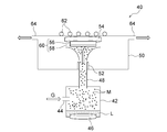
- FIG. 2 shows an example of a mist CVD apparatus.
- the mist generation chamber 42 introduces the carrier gas introduction port 44 into which the carrier gas G is introduced, the ultrasonic vibrator 46 provided in the mist generation chamber 42, and the mist M generated in the mist generation chamber 42 in the film formation chamber 50. It is provided with a duct 48 for transporting to.
- the raw material solution L is housed in the mist generation chamber 42.
- the ultrasonic vibrator 46 is configured to apply ultrasonic vibration to the raw material solution L to generate mist M together with the carrier gas G.
- the film forming chamber 50 is provided with a nozzle 52 for spraying the mist M introduced through the duct 48 onto the substrate 56, a stage 54 to which the substrate 56 is fixed, and the stage 54 and the substrate near the back surface of the stage 54.
- a heater 62 for heating the 56 and an exhaust port 64 for discharging the carrier gas G are provided.
- the raw material solution L used in the mist CVD method is not limited as long as it is a solution that can obtain an ⁇ -Ga 2 O 3 system semiconductor film, and examples thereof include a solution in which Ga is dissolved in a solvent.
- a solution of the dopant component may be added to the raw material solution.
- an additive such as hydrochloric acid may be added to the raw material solution. Water, alcohol, or the like can be used as the solvent.
- the obtained raw material solution L is atomized or dropletized to generate mist M or droplets.
- a preferred example of the method of atomizing or atomizing is a method of vibrating the raw material solution L using an ultrasonic vibrator 46.
- the obtained mist M or droplets are conveyed to the film forming chamber 50 using the carrier gas G.
- the carrier gas G is not particularly limited, but one or more of an inert gas such as oxygen, ozone and nitrogen, and a reducing gas such as hydrogen can be used.
- the film forming chamber 50 is provided with a substrate 56.
- the mist M or droplets conveyed to the film forming chamber 50 are thermally decomposed and chemically reacted there to form a semiconductor film 58 on the substrate 56.
- the reaction temperature varies depending on the type of the raw material solution L, but is preferably 300 to 800 ° C, more preferably 400 to 700 ° C.
- the atmosphere in the film forming chamber 50 is not particularly limited as long as a desired semiconductor film can be obtained, and typically, an oxygen gas atmosphere, an inert gas atmosphere, a vacuum atmosphere, a reducing atmosphere, and an air atmosphere. It is selected from one of.
- the composite material 60 obtained by forming a film is surface-treated.
- annealing treatment ion beam treatment, or oxygen plasma ashing is preferable, and annealing treatment is more preferable.
- an RTA (rapid thermal anneal) treatment having a high rate of temperature rise is preferable.
- the heating rate of the annealing treatment is preferably 10 ° C./s or higher, more preferably 30 ° C./s or higher.
- the upper limit of the heating rate is not particularly limited, but is typically 200 ° C./s or less, and more typically 150 ° C./s or less.
- the holding time is preferably 5 to 600 seconds, more preferably 10 to 300 seconds.
- the annealing treatment temperature is preferably 300 ° C. to 650 ° C., more preferably 350 ° C. to 600 ° C.
- the atmosphere of the annealing treatment is preferably under the atmosphere, under nitrogen, under vacuum, under the inert gas, or under the reducing gas, and more preferably under nitrogen, under vacuum, or under the inert gas.
- the composite material 60 obtained by the annealing treatment is further subjected to the above-mentioned (2) film formation and the above-mentioned (3) surface treatment.
- the total number of times of film formation and surface treatment is preferably 2 times or more, more preferably 10 times or more, and further preferably 20 times or more.
- the emission intensity of 400 to 420 nm can be made relatively larger than the emission intensity of 320 to 340 nm in the CL spectrum of the obtained semiconductor film. .. That is, it is possible to obtain a semiconductor film in which cracks are further reduced (a crack suppressing effect is sufficiently obtained).
- the upper limit of the total number of times of film formation and surface treatment is not particularly limited, but is typically 100 or less, and more typically 80 or less.
- the semiconductor film thus obtained can be formed as it is or divided into semiconductor elements.
- the semiconductor film may be peeled off from the underlying substrate to form a single film.
- a peeling layer may be provided in advance on the surface (deposition surface) of the base substrate.
- Examples of such a release layer include those provided with a C injection layer and an H injection layer on the surface of the base substrate. Further, C or H may be injected into the film at the initial stage of film formation of the semiconductor film, and a release layer may be provided on the semiconductor film side.
- a support substrate (mounting substrate) different from the substrate is bonded and bonded to the surface of the semiconductor film formed on the substrate (that is, the surface opposite to the substrate), and then the semiconductor film is bonded to the substrate. It is also possible to peel off and remove.
- a support substrate (mounting substrate) a substrate having a coefficient of thermal expansion at 25 to 400 ° C. of 6 to 13 ppm / K, for example, a substrate composed of a Cu—Mo composite metal can be used.
- known methods such as brazing, soldering, and solid phase bonding can be mentioned.
- an electrode such as an ohmic electrode or a Schottky electrode, or another layer such as an adhesive layer may be provided between the semiconductor film and the support substrate.
- a functional layer such as a drift layer is formed on the semiconductor film.
- Known methods are also possible for forming functional layers such as drift layers, and preferred examples include various CVD methods, HVPE methods, MBE methods, PLD methods, vapor deposition methods such as sputtering methods, and hydrothermal methods.
- the liquid phase film forming method such as the above is mentioned, and the mist CVD method, the hydrothermal method, or the HVPE method is more preferable.
- Example 1 Fabrication of ⁇ -Ga 2 O 3 series semiconductor film by mist CVD method (1a) Preparation of base substrate As a base substrate, a c-plane sapphire substrate with a thickness of 1.3 mm and a diameter of 15.24 cm (6 inches) (off). Angle 0 °) was prepared.
- a mist CVD apparatus 40 having the configuration shown in FIG. 2 was prepared.
- the configuration of the mist CVD apparatus 40 is as described above.
- the raw material solution L obtained in (1b) above was housed in the mist generation chamber 42.
- a c-plane sapphire substrate having a diameter of 15.24 cm (6 inches) was set on the stage 54 as the substrate 56, and the distance between the tip of the nozzle 52 and the substrate 56 was set to 120 mm.
- the temperature of the stage 54 was raised to 440 ° C. by the heater 62 and held for 30 minutes for temperature stabilization.
- the flow rate control valve (not shown) was opened to supply nitrogen gas as the carrier gas G into the film forming chamber 50 via the mist generation chamber 42, and the atmosphere of the film forming chamber 50 was sufficiently replaced with the carrier gas G. After that, the flow rate of the carrier gas G was adjusted to 1.5 L / min.
- the raw material solution L was atomized by the ultrasonic transducer 46, and the generated mist M was introduced into the film forming chamber 50 by the carrier gas G.
- the semiconductor film 58 was formed on the substrate 56 for 25 minutes by reacting the mist M in the film forming chamber 50, particularly on the surface of the substrate 56 (specifically, the sapphire substrate). In this way, a composite material 60 composed of the substrate 56 and the semiconductor film 58 formed on the substrate 56 was obtained.
- the Ga oxide film has a biaxially oriented corundum-type crystal structure that is oriented in the c-axis direction in the normal direction of the substrate and also in the in-plane direction. From these results, it was confirmed that the semiconductor film 58 obtained in (1f) above is an alignment film having a corundum-type crystal structure composed of ⁇ -Ga 2 O 3.
- the emission intensities of all the obtained CL image measurement points were arithmetically averaged to obtain the integrated value A of the emission intensity at the wavelength of 320 to 340 nm and the integrated value B of the emission intensity at the wavelength of 400 to 420 nm. Then, the value of B / (A + B) was calculated. The results were as shown in Table 1.
- Example 2 Except that the film formation time in (1d) was 15 minutes and the film formation and surface treatment cycle was repeated 23 times in (1f) (that is, the film formation and surface treatment cycle was performed 24 times in total). Film formation and various evaluations were performed in the same manner as in Example 1. From the results of the surface EDX and the surface EBSD, it was confirmed that the obtained semiconductor film was an alignment film having a corundum-type crystal structure composed of ⁇ -Ga 2 O 3. Other results were as shown in Table 1.
- Example 3 Except that the film formation time in (1d) was 10 minutes and the film formation and surface treatment cycle was repeated 34 times in (1f) (that is, the film formation and surface treatment cycle was performed 35 times in total). Film formation and various evaluations were performed in the same manner as in Example 1. From the results of the surface EDX and the surface EBSD, it was confirmed that the obtained semiconductor film was an alignment film having a corundum-type crystal structure composed of ⁇ -Ga 2 O 3. Other results were as shown in Table 1.
- Example 4 Except that the film formation time in (1d) was 5 minutes and the film formation and surface treatment cycle was repeated 69 times in (1f) (that is, the film formation and surface treatment cycle was performed 70 times in total). Film formation and various evaluations were performed in the same manner as in Example 1. From the results of the surface EDX and the surface EBSD, it was confirmed that the obtained semiconductor film was an alignment film having a corundum-type crystal structure composed of ⁇ -Ga 2 O 3. Other results were as shown in Table 1.
- Example 5 The film formation and various evaluations were carried out in the same manner as in Example 4 except that the helium atmosphere was used instead of the nitrogen atmosphere in (1e) above. From the results of the surface EDX and the surface EBSD, it was confirmed that the obtained semiconductor film was an alignment film having a corundum-type crystal structure composed of ⁇ -Ga 2 O 3. Other results were as shown in Table 1.
- Example 6 (comparison) The film formation and various evaluations are the same as in Example 1 except that the film formation time of the above (1d) is 360 minutes and the surface treatment of the above (1e) and the re-deposition and resurface treatment of the above (1f) are not performed. Was done. From the results of the surface EDX and the surface EBSD, it was confirmed that the obtained semiconductor film was an alignment film having a corundum-type crystal structure composed of ⁇ -Ga 2 O 3. Other results were as shown in Table 1.
Landscapes
- Chemical & Material Sciences (AREA)
- Engineering & Computer Science (AREA)
- Crystallography & Structural Chemistry (AREA)
- Materials Engineering (AREA)
- Metallurgy (AREA)
- Organic Chemistry (AREA)
- Inorganic Chemistry (AREA)
- Chemical Kinetics & Catalysis (AREA)
- General Chemical & Material Sciences (AREA)
- Crystals, And After-Treatments Of Crystals (AREA)
- Liquid Deposition Of Substances Of Which Semiconductor Devices Are Composed (AREA)
Abstract
成膜用下地基板の用意に手間をかけずとも大面積で厚くかつクラックが低減されたα-Ga2O3系半導体膜が提供される。この半導体膜は、α-Ga2O3で構成されるコランダム型結晶構造を有し、25℃で測定したカソードルミネッセンス(CL)スペクトルにおいて、320~340nmの発光強度の積分値A、及び400~420nmの発光強度の積分値Bが、B/(A+B)>0.15の関係を満たす。
Description
本発明は、α-Ga2O3系半導体膜に関するものである。
近年、酸化ガリウム(Ga2O3)が半導体用材料として着目されている。酸化ガリウムはα、β、γ、δ及びεの5つの結晶形を有することが知られているが、この中で、準安定相であるα-Ga2O3はバンドギャップが5.3eVと非常に大きく、パワー半導体用材料として期待を集めている。
例えば、特許文献1(特開2014-72533号公報)には、コランダム型結晶構造を有する下地基板と、コランダム型結晶構造を有する半導体層と、コランダム型結晶構造を有する絶縁膜とを備えた半導体装置が開示されており、サファイア基板上に、半導体層としてα-Ga2O3膜を成膜した例が記載されている。また、特許文献2(特開2016-25256号公報)には、コランダム構造を有する結晶性酸化物半導体を主成分として含むn型半導体層と、六方晶の結晶構造を有する無機化合物を主成分とするp型半導体層と、電極とを備えた半導体装置が開示されている。この特許文献2の実施例には、c面サファイア基板上に、n型半導体層として準安定相であるコランダム構造を有するα-Ga2O3膜を、p型半導体層として六方晶の結晶構造を有するα-Rh2O3膜を形成して、ダイオードを作製することが開示されている。
ところで、異種基板上にα-Ga2O3膜を結晶成長させる際に、クラックが生じるという問題がある。α-Ga2O3と異種コランダム材料との混晶であるInAlGaO系の半導体膜を成膜する際も、通常、異種基板上に結晶成長を行うため、エピタキシャル膜にクラックが入る等の問題が生じている。この問題に対処する技術として、特許文献3(特開2016-100592号公報)では、クラックの少ないα-Ga2O3膜を作製することが開示されている。また、特許文献4(特開2016-100593号公報)には、エピタキシャル膜の成膜時にボイドを含ませることにより、クラックが低減されたα-Ga2O3膜を作製することが開示されている。
さらに、特許文献5(特開2018-2544号公報)には、2層以上の酸化物層が形成されている成膜用下地基板を用いることで、大面積で実質的にクラックを含まない結晶性酸化物半導体膜を得た例が開示されている。
Xing Lu, Leidang Zhou, Liang Chen, Xiaoping Ouyang, Huili Tang, Bo Liu, and Jun Xu, "X-ray Detection Performance of Vertical Schottky PhotodiodesBased on a Bulk β-Ga2O3 Substrate Grown by an EFG Method," ECS Journal of Solid State Science and Technology, 8 (7) Q3046-Q3049 (2019)
金子健太郎「コランダム構造酸化ガリウム系混晶薄膜の成長と物性」、京都大学、発行日:2013年3月25日(許諾条件により要旨・本文は2014年1月31日に公開)、URL: https://doi.org/10.14989/doctor.k17573
藤田静雄、大島孝仁及び金子健太郎、「酸化ガリウム半導体の表面制御と高品質単結晶薄膜の作製」、表面科学Vol.31, No.12, pp.643-650, 2010
四戸孝、「ミストCVD法による各種薄膜形成技術」、THE CHEMICAL TIMES、通巻254号、8~11頁、2019年
しかしながら、特許文献3及び4に記載されるようなクラックを低減する手法によっては、大面積にわたってクラックを実質的に含まないα-Ga2O3系半導体膜を得ることが難しく、特に3μm以上の厚膜とした場合には、クラックが十分に低減された半導体膜を得ることができていなかった。これに対して、特許文献5には、上述のとおり大面積で実質的にクラックを含まない結晶性酸化物半導体膜が開示されている。しかし、下地基板上に複数の層を形成する必要があり、作業が煩雑でコスト的にも不利となる。そのため、成膜用下地基板の用意に手間をかけず(例えば下地基板としてサファイア基板を用いる)、大面積で膜厚を大きくした場合においてもクラックが生じにくいα-Ga2O3系半導体膜が望まれている。
本発明者らは、今般、α-Ga2O3系半導体膜について、カソードルミネッセンススペクトル(以下、CLスペクトルということがある)における特定範囲の波長での発光強度を制御することにより、成膜用下地基板の用意に手間をかけずとも大面積で厚くかつクラックが生じにくい膜が得られることを知見した。
したがって、本発明の目的は、成膜用下地基板の用意に手間をかけずとも大面積で厚くかつクラックが低減されたα-Ga2O3系半導体膜を提供することにある。
本発明の一態様によれば、α-Ga2O3で構成されるコランダム型結晶構造を有する半導体膜であって、
25℃で測定したカソードルミネッセンス(CL)スペクトルにおいて、320~340nmの発光強度の積分値A、及び400~420nmの発光強度の積分値Bが、B/(A+B)>0.15の関係を満たす、半導体膜が提供される。
25℃で測定したカソードルミネッセンス(CL)スペクトルにおいて、320~340nmの発光強度の積分値A、及び400~420nmの発光強度の積分値Bが、B/(A+B)>0.15の関係を満たす、半導体膜が提供される。
本発明の別の一態様によれば、サファイア基板と、前記サファイア基板上に形成された前記半導体膜とを備えた、複合材料が提供される。
半導体膜
本発明の半導体膜は、α-Ga2O3で構成されるコランダム型結晶構造を有する。α-Ga2O3は、三方晶系の結晶群に属し、コランダム型結晶構造をとる。また、この半導体膜は、25℃で測定したCLスペクトルにおいて、320~340nmの発光強度の積分値A、及び400~420nmの発光強度の積分値Bが、B/(A+B)>0.15の関係を満たす。このようにα-Ga2O3系半導体膜について、CLスペクトルにおける特定範囲の波長での発光強度を制御することにより、成膜用下地基板の用意に手間をかけずとも大面積で厚くかつクラックが生じにくい膜が得られる。前述したように、従来技術においては、大面積で厚くクラックが少ない半導体膜を得ることは困難であり、また、このような半導体膜を得ようとする場合は下地基板上に複数の層を形成する必要があり、作業が煩雑でコスト的にも不利であった。この点、本発明の半導体膜によればこれらの問題を好都合に解消することができる。
本発明の半導体膜は、α-Ga2O3で構成されるコランダム型結晶構造を有する。α-Ga2O3は、三方晶系の結晶群に属し、コランダム型結晶構造をとる。また、この半導体膜は、25℃で測定したCLスペクトルにおいて、320~340nmの発光強度の積分値A、及び400~420nmの発光強度の積分値Bが、B/(A+B)>0.15の関係を満たす。このようにα-Ga2O3系半導体膜について、CLスペクトルにおける特定範囲の波長での発光強度を制御することにより、成膜用下地基板の用意に手間をかけずとも大面積で厚くかつクラックが生じにくい膜が得られる。前述したように、従来技術においては、大面積で厚くクラックが少ない半導体膜を得ることは困難であり、また、このような半導体膜を得ようとする場合は下地基板上に複数の層を形成する必要があり、作業が煩雑でコスト的にも不利であった。この点、本発明の半導体膜によればこれらの問題を好都合に解消することができる。
CLスペクトルの発光強度を測定して積分値A及びBを算出する方法は特に限定されないが、例えば以下のとおりである。
1)まず、各波長において、半導体膜表面の5μm×5μmの領域でCLスペクトルの発光強度を10視野測定し、得られた発光強度を算術平均する。このときの10視野分の発光強度の算術平均値は、5μm×5μmの領域をスキャニングしてエリア分析して算出してもよいし、5μm×5μmの領域の中である間隔ごとに点分析し得られた全点のCLスペクトルの発光強度を算術平均して算出してもよい。このようにして、各波長における、それぞれのCLスペクトルの発光強度Xを算出する。
2)そして、得られた各波長における発光強度Xのうち、320~340nmの波長における発光強度Xを全て足し合わせたものを積分値Aとする。例えば、発光強度Xが、0.41nmの波長毎にデータ出力された場合(すなわち、320.00nm、320.41nm、320.82nm、といった波長毎にデータ入力された場合)、320nm以上340nm未満の各波長における発光強度Xを合計したものを積分値Aとする(すなわち、積分値Aに320.00nmの発光強度は含まれるが、340.00nmの発光強度は含まれない)。
3)400~420nmの波長においても上記2)と同様にして、400nm以上420nm未満の各波長における発光強度Xを合計したものを積分値Bとする。なお、320~340nmのピークと400~420nmのピークとの関係性は特に限定されない。例えば、それぞれのピークが明確に分離できてもよく、ショルダーピークになっていてもよく、分離できなくてもよい。このようにCLスペクトル測定により現れるピーク全体の形状は特に限定されず、320~340nmのピークと400~420nmのピークから積分値A及びBを求めることができればよい。
このようにして、積分値A及びBを算出することが考えられる。
このように、本発明の半導体膜には、CLスペクトル測定において320~340nmのピークと400~420nmのピークとが現れうる。この点、従来より、α-Ga2O3のCLスペクトルを測定すると320~340nm付近にピークが現れることが知られている(例えば特許文献6を参照)。一方、本発明の半導体膜では、400~420nmにもピークが現れ、320~340nmの発光強度に対して400~420nmの発光強度が大きくなるにつれてクラックが低減される。
酸化ガリウムはα、β、γ、δ及びεの5つの結晶形を有することが知られている。本発明のα-Ga2O3系半導体膜の他にも、β-Ga2O3のCLスペクトルを測定した例がある。例えば、非特許文献1では、β-Ga2O3のCLスペクトルを測定すると370~415nm付近にピークが現れることが開示されている。しかし、α-Ga2O3とβ-Ga2O3は、双方の結晶構造が全く異なり全く別の材料といえるため、得られるCLスペクトルの傾向も異なる。また、クラックが低減されるという観点において、好ましいβ-Ga2O3のCLスペクトルのピーク位置や発光強度も不明である。以下、α-Ga2O3とβ-Ga2O3が全く異なる材料であることを具体的に説明する。
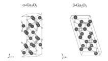
1)図1に示されるように、β-Ga2O3の結晶構造は単斜晶系βガリア構造であるのに対して、α-Ga2O3の結晶構造はコランダム構造である(例えば非特許文献2を参照)。また、結晶の配位数はα-Ga2O3が6配位であるのに対し、β-Ga2O3では4配位と6配位が混在している。さらに、α-Ga2O3ではへき開面は存在しないが、β-Ga2O3ではへき開面が(100)面と(001)面の2つ存在する(例えば非特許文献3を参照)。
2)α-Ga2O3とβ-Ga2O3は物性が異なる。光学バンドギャップはα-Ga2O3では5.3eVであるのに対して、β-Ga2O3では4.9eVである(例えば非特許文献2を参照)。また、パワーデバイスにどの程度適しているかを示す基本性能指標であるバリガ性能指数はα-Ga2O3が6726(εμEc 3)であるのに対し、β-Ga2O3では2307(εμEc 3)である(例えば非特許文献4を参照)。
3)α-Ga2O3とβ-Ga2O3は製造方法が異なる。α-Ga2O3の単結晶バルクの製造方法は一般的には知られていないが、β-Ga2O3の単結晶バルクの製造方法は融液成長法であることが知られており、その中でもEFG(Edge-defined Film-fed Growth)法が著名である。
このように、α-Ga2O3とβ-Ga2O3は全く異なる材料である。
本発明の半導体膜は、積分値A及び積分値Bが、B/(A+B)>0.15の関係を満たす。また、好ましくはB/(A+B)>0.50、より好ましくはB/(A+B)>0.70の関係を満たす。こうすることで、大面積で厚くかつクラックが低減された半導体膜を効果的に得ることができる。B/(A+B)の値が大きいほどクラックが低減された半導体膜となるため、B/(A+B)の値の上限は特に限定されないが、典型的にはB/(A+B)は0.90未満である。これは、α-Ga2O3系半導体膜をCLスペクトル測定すると、320~340nm付近及び400~420nm付近のいずれにおいても少なからず発光するためである。そこで、本発明の半導体膜のように、400~420nmの発光強度を大きくすることにより、成膜用下地基板の用意に手間をかけずとも大面積で厚くかつクラックが低減された半導体膜とすることができる。
本発明の半導体膜の面積は10.0~729.7cm2であるのが好ましく、より好ましくは19.6~729.7cm2、さらに好ましくは30.0~729.7cm2である。このような大面積の半導体膜では、従来クラックを少なくすることは困難であったところ、本発明の半導体膜によれば、成膜用下地基板の用意に手間をかけずともクラックを低減することができる。また、半導体膜は円形状でありうる。その場合、半導体膜は直径3.6~30.5cmであるのが好ましく、より好ましくは直径5.0~30.5cm、さらに好ましくは直径6.0~30.5cmである。なお、本明細書において、「円形状」とは、完全な円形状である必要はなく、全体として概ね円形と認識されうる略円形状であってもよい。例えば、円形の一部が切り欠かれた形状であってもよい。この場合、半導体膜の直径は、切り欠き部分が無いものと仮定した場合に想定される円形状に基づいて決定すればよい。
本発明の半導体膜の厚さは1μm以上であるのが好ましく、より好ましくは3μm以上、さらに好ましくは7μm以上である。このような厚い半導体膜では、従来クラックを少なくすることは困難であったところ、本発明の半導体膜によれば、成膜用下地基板の用意に手間をかけずともクラックを低減することができる。膜厚の上限は特に限定されず、コスト面及び要求される特性の観点から適宜調整すればよいが、例えば1000μm以下、700μm以下又は500μm以下である。
本発明のドーパントとして14族元素を含むことができる。ここで、14族元素はIUPAC(国際純正・応用化学連合)が策定した周期律表による第14族元素のことであり、具体的には、炭素(C)、珪素(Si)、ゲルマニウム(Ge)、錫(Sn)及び鉛(Pb)のいずれかの元素である。半導体膜におけるドーパント(14族元素)の含有量は、好ましくは1.0×10¹⁶~1.0×10²¹/cm3、より好ましくは1.0×1017~1.0×1019/cm3である。これらのドーパントは膜中に均質に分布し、半導体膜の表面と裏面のドーパント濃度は同程度であることが好ましい。
下地基板上に作製した半導体膜を分離し、別の支持基板に転載してもよい。別の支持基板の材質は特に限定はないが、材料物性の観点から好適なものを選択すればよい。例えば、熱伝導率の観点では、Cu等の金属基板、SiC、AlN等のセラミックス基板等が好ましい。また、25~400℃での熱膨張率が6~13ppm/Kである基板を用いるのも好ましい。このような熱膨張率を有する支持基板を用いることで、半導体膜との熱膨張差を小さくすることができ、その結果、熱応力による半導体膜中のクラック発生や膜剥がれ等を抑制できる。このような支持基板の例としては、Cu-Mo複合金属で構成される基板が挙げられる。CuとMoの複合比率は、半導体膜との熱膨張率マッチング、熱伝導率、導電率等を勘案して、適宜選択することができる。
複合材料
本発明の好ましい態様によれば、サファイア基板と、サファイア基板上に形成された本発明の半導体膜とを備えた複合材料が提供される。下地基板としてサファイア基板を用いることにより、成膜用下地基板の用意に手間をかけることがない。加えて、サファイア基板上に本発明の半導体膜を形成することにより、大面積で厚くかつクラックが低減された半導体膜を備えた複合材料が得られる。
本発明の好ましい態様によれば、サファイア基板と、サファイア基板上に形成された本発明の半導体膜とを備えた複合材料が提供される。下地基板としてサファイア基板を用いることにより、成膜用下地基板の用意に手間をかけることがない。加えて、サファイア基板上に本発明の半導体膜を形成することにより、大面積で厚くかつクラックが低減された半導体膜を備えた複合材料が得られる。
半導体膜の製造方法
本発明の半導体膜は、成膜用下地基板の用意に手間をかけずとも大面積で厚くかつクラックが低減されたものを得られる限り、その製法は特に限定されるものではない。以下に、本発明の半導体膜の製造方法を、(1)下地基板の準備、(2)成膜、(3)表面処理、並びに(4)再成膜及び再表面処理の順に説明する。
本発明の半導体膜は、成膜用下地基板の用意に手間をかけずとも大面積で厚くかつクラックが低減されたものを得られる限り、その製法は特に限定されるものではない。以下に、本発明の半導体膜の製造方法を、(1)下地基板の準備、(2)成膜、(3)表面処理、並びに(4)再成膜及び再表面処理の順に説明する。
(1)下地基板の準備
まず、下地基板としてサファイア基板を用意する。このようにサファイア基板自体を成膜用下地基板として用いることで、成膜用下地基板の用意に手間をかけることなく半導体膜を形成することができる。用いるサファイア基板は、いずれの方位面を有するものであってもよい。すなわち、a面、c面、r面、m面を有するものであってもよく、これらの面に対して所定のオフ角を有するものであってもよい。例えばc面サファイアを用いた場合、表面に対してc軸配向しているため、その上に、容易にc軸配向させた半導体膜をヘテロエピタキシャル成長させることが可能となる。また、電気特性を調整するために、ドーパントを加えたサファイア基板を用いることも可能である。このようなドーパントとしては公知のものが使用可能である。
まず、下地基板としてサファイア基板を用意する。このようにサファイア基板自体を成膜用下地基板として用いることで、成膜用下地基板の用意に手間をかけることなく半導体膜を形成することができる。用いるサファイア基板は、いずれの方位面を有するものであってもよい。すなわち、a面、c面、r面、m面を有するものであってもよく、これらの面に対して所定のオフ角を有するものであってもよい。例えばc面サファイアを用いた場合、表面に対してc軸配向しているため、その上に、容易にc軸配向させた半導体膜をヘテロエピタキシャル成長させることが可能となる。また、電気特性を調整するために、ドーパントを加えたサファイア基板を用いることも可能である。このようなドーパントとしては公知のものが使用可能である。
(2)成膜
次に、下地基板上にα-Ga2O3系半導体膜を形成する。半導体膜の形成手法としては、大面積で厚くかつクラックが低減された半導体膜が得られる限り、公知の手法が採用可能である。しかしながら、各種CVD法、HVPE法、MBE法、PLD法及びスパッタリング法等の気相成膜法、水熱法等の液相成膜法のいずれかが好ましい。CVD法の例としては、熱CVD法、プラズマCVD法、ミストCVD法、MO(有機金属)CVD法等が挙げられる。これらの中では、ミストCVD法、水熱法、又はHVPE法がより好ましい。ミストCVD法について以下に説明する。
次に、下地基板上にα-Ga2O3系半導体膜を形成する。半導体膜の形成手法としては、大面積で厚くかつクラックが低減された半導体膜が得られる限り、公知の手法が採用可能である。しかしながら、各種CVD法、HVPE法、MBE法、PLD法及びスパッタリング法等の気相成膜法、水熱法等の液相成膜法のいずれかが好ましい。CVD法の例としては、熱CVD法、プラズマCVD法、ミストCVD法、MO(有機金属)CVD法等が挙げられる。これらの中では、ミストCVD法、水熱法、又はHVPE法がより好ましい。ミストCVD法について以下に説明する。
ミストCVD法は、原料溶液を霧化又は液滴化してミスト又は液滴を発生させ、キャリアガスを用いてミスト又は液滴を基板を備えた成膜室に搬送し、成膜室内でミスト又は液滴を熱分解及び化学反応させて基板上に膜を形成及び成長させる手法であり、真空プロセスを必要とせず、短時間で大量のサンプルを作製することができる。図2にミストCVD装置の一例を示す。図2に示されるミストCVD装置40は、キャリアガスG及び原料溶液LからミストMを発生させるミスト発生室42と、ミストMを基板56に吹き付けて熱分解及び化学反応を経て半導体膜58を形成する成膜室50とを有する。ミスト発生室42は、キャリアガスGが導入されるキャリアガス導入口44と、ミスト発生室42内に設けられる超音波振動子46と、ミスト発生室42内で発生したミストMを成膜室50に搬送するダクト48とを備えている。ミスト発生室42内には原料溶液Lが収容される。超音波振動子46は、原料溶液Lに超音波振動を与えてキャリアガスGとともにミストMを発生できるように構成される。成膜室50は、ダクト48を介して導入されるミストMを基板56に吹き付けるためのノズル52と、基板56が固定されるステージ54と、ステージ54の裏面近傍に設けられてステージ54及び基板56を加熱するためのヒータ62と、キャリアガスGを排出するための排気口64とを備える。
ミストCVD法に用いる原料溶液Lとしては、α-Ga2O3系半導体膜が得られる溶液であれば、限定されるものではないが、例えば、Gaを溶媒に溶解させたものが挙げられる。また、半導体層にドーパントを加える場合には、原料溶液にドーパント成分の溶液を加えてもよい。さらに、原料溶液には塩酸等の添加剤を加えてもよい。溶媒としては水やアルコール等を使用することができる。
次に、得られた原料溶液Lを霧化又は液滴化してミストM又は液滴を発生させる。霧化又は液滴化する方法の好ましい例としては、超音波振動子46を用いて原料溶液Lを振動させる手法が挙げられる。その後、得られたミストM又は液滴を、キャリアガスGを用いて成膜室50に搬送する。キャリアガスGとしては特に限定されるものではないが、酸素、オゾン、窒素等の不活性ガス、及び水素等の還元ガスの一種又は二種以上を用いることができる。
成膜室50には基板56が備えられている。成膜室50に搬送されたミストM又は液滴は、そこで熱分解及び化学反応されて、基板56上に半導体膜58を形成する。反応温度は原料溶液Lの種類に応じて異なるが、好ましくは300~800℃、より好ましくは400~700℃である。また、成膜室50内の雰囲気は、所望の半導体膜が得られる限り特に限定されるものではなく、典型的には、酸素ガス雰囲気、不活性ガス雰囲気、真空雰囲気、還元雰囲気、及び大気雰囲気のいずれかから選択される。
(3)表面処理
成膜して得られた複合材料60に、表面処理を行う。この表面処理に用いられる方法としては、アニール処理、イオンビーム処理、又は酸素プラズマアッシングが好ましく、アニール処理がより好ましい。さらに、アニール処理としては、昇温速度が速いRTA(rapid thermal anneal)処理が好ましい。
成膜して得られた複合材料60に、表面処理を行う。この表面処理に用いられる方法としては、アニール処理、イオンビーム処理、又は酸素プラズマアッシングが好ましく、アニール処理がより好ましい。さらに、アニール処理としては、昇温速度が速いRTA(rapid thermal anneal)処理が好ましい。
アニール処理の昇温速度は10℃/s以上が好ましく、30℃/s以上がより好ましい。昇温速度の上限は特に限定されないが、典型的には200℃/s以下であり、より典型的には150℃/s以下である。
アニール処理において、保持時間は5~600秒間であるのが好ましく、10~300秒間であるのがより好ましい。
アニール処理温度は300℃~650℃が好ましく、350℃~600℃がより好ましい。
アニール処理の雰囲気は大気下、窒素下、真空下、不活性ガス下、又は還元ガス下であるのが好ましく、窒素下、真空下又は不活性ガス下であるのがより好ましい。
(4)再成膜及び再表面処理
アニール処理して得られた複合材料60に、さらに上記(2)の成膜及び上記(3)の表面処理を繰り返し行う。成膜及び表面処理を行う合計回数としては、2回以上が好ましく、10回以上がより好ましく、20回以上がさらに好ましい。このように成膜及び表面処理を行う合計回数を多くすることで、得られる半導体膜のCLスペクトルにおいて、400~420nmの発光強度を320~340nmの発光強度よりも相対的に大きくすることができる。すなわち、クラックがより低減された(クラック抑制効果を充分に得られた)半導体膜を得ることができる。成膜及び表面処理を行う合計回数の上限は特に限定されないが、典型的には100回以下であり、より典型的には80回以下である。
アニール処理して得られた複合材料60に、さらに上記(2)の成膜及び上記(3)の表面処理を繰り返し行う。成膜及び表面処理を行う合計回数としては、2回以上が好ましく、10回以上がより好ましく、20回以上がさらに好ましい。このように成膜及び表面処理を行う合計回数を多くすることで、得られる半導体膜のCLスペクトルにおいて、400~420nmの発光強度を320~340nmの発光強度よりも相対的に大きくすることができる。すなわち、クラックがより低減された(クラック抑制効果を充分に得られた)半導体膜を得ることができる。成膜及び表面処理を行う合計回数の上限は特に限定されないが、典型的には100回以下であり、より典型的には80回以下である。
このようにして得られた半導体膜は、そのままの形態又は分割して半導体素子とすることが可能である。あるいは、半導体膜を下地基板から剥離して膜単体の形態としてもよい。この場合、下地基板からの剥離を容易にするために、下地基板の表面(成膜面)に予め剥離層を設けたものを用いてもよい。このような剥離層は、下地基板表面にC注入層やH注入層を設けたものが挙げられる。また、半導体膜の成膜初期にCやHを膜中に注入させ、半導体膜側に剥離層を設けてもよい。さらに、下地基板上に成膜された半導体膜の表面(すなわち下地基板とは反対側の面)に下地基板とは異なる支持基板(実装基板)を接着及び接合し、その後、半導体膜から下地基板を剥離除去することも可能である。このような支持基板(実装基板)として、25~400℃での熱膨張率が6~13ppm/Kであるもの、例えばCu-Mo複合金属で構成される基板を用いることができる。また、半導体膜と支持基板(実装基板)を接着及び接合する手法の例としては、ロウ付け、半田、固相接合等の公知の手法を挙げることができる。さらに、半導体膜と支持基板との間に、オーミック電極、ショットキー電極等の電極、又は接着層等の他の層を設けてもよい。
パワーデバイス等の半導体素子の製造においては、半導体膜上にドリフト層等の機能層が形成されることになる。ドリフト層等の機能層の形成についても、公知の手法が可能であり、好ましい例としては、各種CVD法、HVPE法、MBE法、PLD法及びスパッタリング法等の気相成膜法、水熱法等の液相成膜法が挙げられ、ミストCVD法、水熱法、又はHVPE法がより好ましい。
本発明を以下の例によってさらに具体的に説明する。
例1
(1)ミストCVD法によるα-Ga2O3系半導体膜の作製
(1a)下地基板の準備
下地基板として、厚さ1.3mmで直径15.24cm(6インチ)のc面サファイア基板(オフ角0°)を準備した。
(1)ミストCVD法によるα-Ga2O3系半導体膜の作製
(1a)下地基板の準備
下地基板として、厚さ1.3mmで直径15.24cm(6インチ)のc面サファイア基板(オフ角0°)を準備した。
(1b)原料溶液の作製
塩酸に金属Gaを添加して室温で3週間撹拌することで、ガリウムイオン濃度が3mol/Lの塩化ガリウム溶液を得た。得られた塩化ガリウム溶液に水を加えてガリウムイオン濃度が90mmol/Lとなるように水溶液を調整した。この水溶液に水酸化アンモニウムを添加してpHを4.0となるように調整し、原料溶液とした。
塩酸に金属Gaを添加して室温で3週間撹拌することで、ガリウムイオン濃度が3mol/Lの塩化ガリウム溶液を得た。得られた塩化ガリウム溶液に水を加えてガリウムイオン濃度が90mmol/Lとなるように水溶液を調整した。この水溶液に水酸化アンモニウムを添加してpHを4.0となるように調整し、原料溶液とした。
(1c)成膜準備
図2に示される構成のミストCVD装置40を準備した。ミストCVD装置40の構成については前述したとおりである。ミストCVD装置40において、上記(1b)で得られた原料溶液Lをミスト発生室42内に収容した。基板56として直径15.24cm(6インチ)のc面サファイア基板をステージ54にセットし、ノズル52の先端と基板56の間の距離を120mmとした。ヒータ62により、ステージ54の温度を440℃にまで昇温させ、温度安定化のため30分保持した。流量調節弁(図示せず)を開いてキャリアガスGとしての窒素ガスを、ミスト発生室42を経て成膜室50内に供給し、成膜室50の雰囲気をキャリアガスGで十分置換した。その後、キャリアガスGの流量を1.5L/minに調節した。
図2に示される構成のミストCVD装置40を準備した。ミストCVD装置40の構成については前述したとおりである。ミストCVD装置40において、上記(1b)で得られた原料溶液Lをミスト発生室42内に収容した。基板56として直径15.24cm(6インチ)のc面サファイア基板をステージ54にセットし、ノズル52の先端と基板56の間の距離を120mmとした。ヒータ62により、ステージ54の温度を440℃にまで昇温させ、温度安定化のため30分保持した。流量調節弁(図示せず)を開いてキャリアガスGとしての窒素ガスを、ミスト発生室42を経て成膜室50内に供給し、成膜室50の雰囲気をキャリアガスGで十分置換した。その後、キャリアガスGの流量を1.5L/minに調節した。
(1d)成膜
超音波振動子46によって原料溶液Lを霧化し、発生したミストMをキャリアガスGによって成膜室50内に導入した。ミストMを成膜室50内、特に基板56(具体的にはサファイア基板)の表面で反応させることによって、基板56上に半導体膜58を25分にわたって形成した。こうして、基板56及びその上に形成された半導体膜58で構成される複合材料60を得た。
超音波振動子46によって原料溶液Lを霧化し、発生したミストMをキャリアガスGによって成膜室50内に導入した。ミストMを成膜室50内、特に基板56(具体的にはサファイア基板)の表面で反応させることによって、基板56上に半導体膜58を25分にわたって形成した。こうして、基板56及びその上に形成された半導体膜58で構成される複合材料60を得た。
(1e)表面処理
成膜して得られた複合材料60に、窒素雰囲気にて昇温速度50℃/sで室温(25℃)から550℃まで昇温し、30秒間保持することにより、RTA(rapid thermal anneal)処理を行った。
成膜して得られた複合材料60に、窒素雰囲気にて昇温速度50℃/sで室温(25℃)から550℃まで昇温し、30秒間保持することにより、RTA(rapid thermal anneal)処理を行った。
(1f)再成膜及び再表面処理
上記(1c)において、基板56として上記(1e)で表面処理した複合材料60を用いたこと以外は同様にして、上記(1d)及び上記(1e)のサイクルを13回繰り返した。すなわち、上記(1d)の成膜及び上記(1e)の表面処理を合計で14回行ったことになる。こうして、クラックが低減されたα-Ga2O3系半導体膜58を備えた複合材料60を得た。この半導体膜の直径は15.24cmであり、面積は182.4cm2であった。これを後述のとおり評価した。
上記(1c)において、基板56として上記(1e)で表面処理した複合材料60を用いたこと以外は同様にして、上記(1d)及び上記(1e)のサイクルを13回繰り返した。すなわち、上記(1d)の成膜及び上記(1e)の表面処理を合計で14回行ったことになる。こうして、クラックが低減されたα-Ga2O3系半導体膜58を備えた複合材料60を得た。この半導体膜の直径は15.24cmであり、面積は182.4cm2であった。これを後述のとおり評価した。
(2)評価
(2a)表面EDX
上記(1f)で得られた半導体膜58の表面に対してエネルギー分散型X線分析(EDX)による組成分析を行った結果、Ga及びOのみが検出された。このことから、この半導体膜58はGa酸化物で構成されることが分かった。
(2a)表面EDX
上記(1f)で得られた半導体膜58の表面に対してエネルギー分散型X線分析(EDX)による組成分析を行った結果、Ga及びOのみが検出された。このことから、この半導体膜58はGa酸化物で構成されることが分かった。
(2b)断面SEM
上記(1f)で得られた半導体膜58の断面試験片を切出し、走査型電子顕微鏡(日本電子製JSM-IT500LA)を用いて断面SEM観察を行った。得られたSEM像からGa酸化物の厚さを測定したところ、7.1μmであった。
上記(1f)で得られた半導体膜58の断面試験片を切出し、走査型電子顕微鏡(日本電子製JSM-IT500LA)を用いて断面SEM観察を行った。得られたSEM像からGa酸化物の厚さを測定したところ、7.1μmであった。
(2c)表面EBSD
上記(1f)で得られた半導体膜58において、電子線後方散乱回折装置(EBSD)(オックスフォード・インストゥルメンツ社製Nordlys Nano)を取り付けたSEM(日立ハイテクノロジーズ社製、SU-5000)にて、Ga酸化物膜表面の逆極点図方位マッピングを500μm×500μmの視野で実施した。このEBSD測定の諸条件は以下のとおりとした。
上記(1f)で得られた半導体膜58において、電子線後方散乱回折装置(EBSD)(オックスフォード・インストゥルメンツ社製Nordlys Nano)を取り付けたSEM(日立ハイテクノロジーズ社製、SU-5000)にて、Ga酸化物膜表面の逆極点図方位マッピングを500μm×500μmの視野で実施した。このEBSD測定の諸条件は以下のとおりとした。
<EBSD測定条件>
・加速電圧:15kV
・スポット強度:70
・ワーキングディスタンス:22.5mm
・ステップサイズ:0.5μm
・試料傾斜角:70°
・測定プログラム:Aztec(version 3.3)
・加速電圧:15kV
・スポット強度:70
・ワーキングディスタンス:22.5mm
・ステップサイズ:0.5μm
・試料傾斜角:70°
・測定プログラム:Aztec(version 3.3)
得られた逆極点図方位マッピングから、Ga酸化物膜は、基板法線方向にc軸配向するとともに、面内方向にも配向した二軸配向のコランダム型結晶構造を有することが分かった。これらの結果から、上記(1f)で得られた半導体膜58はα-Ga2O3で構成されるコランダム型結晶構造の配向膜であることが確認された。
(2d)平面CL強度マッピング測定
上記(1f)で得られた半導体膜58について、CL分光装置(分光器:堀場製作所製iHR-320、SEM:日本電子製ショットキーエミッション型SEM JSM-7100F/TTLS)にて、平面CL強度マッピング測定を5μm×5μmの視野で10視野実施した。この平面CL強度マッピング測定の諸条件は以下のとおりとした。
上記(1f)で得られた半導体膜58について、CL分光装置(分光器:堀場製作所製iHR-320、SEM:日本電子製ショットキーエミッション型SEM JSM-7100F/TTLS)にて、平面CL強度マッピング測定を5μm×5μmの視野で10視野実施した。この平面CL強度マッピング測定の諸条件は以下のとおりとした。
<平面CL強度マッピング測定条件>
・検出器:CCD(Jobin Yvon)
・分光器の回折格子:100gr/mm、ブレーズ波長450nm
・CL像画素数:51×51
・CLスペクトル積算時間:10ms×1
・測定温度:室温(25℃)
・照射電流:4.8nA
・加速電圧:10kV
・W.D.:10.3mm
・SEM像画素数:250×250
・検出器:CCD(Jobin Yvon)
・分光器の回折格子:100gr/mm、ブレーズ波長450nm
・CL像画素数:51×51
・CLスペクトル積算時間:10ms×1
・測定温度:室温(25℃)
・照射電流:4.8nA
・加速電圧:10kV
・W.D.:10.3mm
・SEM像画素数:250×250
得られた全CL像測定点の発光強度を算術平均し、320~340nmの波長の発光強度の積分値A、及び400~420nmの波長の発光強度の積分値Bを求めた。そして、B/(A+B)の値を算出した。結果は表1に示されるとおりであった。
(2e)クラック評価
工業用顕微鏡(ニコン製ECLIPSE LV150N)を用いて、接眼レンズを10倍、対物レンズを5倍とし、偏光・微分干渉モードにて膜表面全体を観察し、クラックが確認された場合は対物レンズを10倍に変更し、画像を取得した。そして、長さ50μm以上のクラックのみ、クラックとしてカウントした。また、あるクラックから別のクラックまでの距離が500μm以下の場合は一つのクラックとみなした。結果は表1に示されるとおりであった。
工業用顕微鏡(ニコン製ECLIPSE LV150N)を用いて、接眼レンズを10倍、対物レンズを5倍とし、偏光・微分干渉モードにて膜表面全体を観察し、クラックが確認された場合は対物レンズを10倍に変更し、画像を取得した。そして、長さ50μm以上のクラックのみ、クラックとしてカウントした。また、あるクラックから別のクラックまでの距離が500μm以下の場合は一つのクラックとみなした。結果は表1に示されるとおりであった。
例2
上記(1d)の成膜時間を15分とし、上記(1f)において成膜と表面処理のサイクルを23回繰り返した(すなわち、成膜と表面処理のサイクルを合計24回行った)こと以外は例1と同様にして成膜及び各種評価を行った。表面EDX及び表面EBSDの結果より、得られた半導体膜はα-Ga2O3で構成されるコランダム型結晶構造の配向膜であることが確認された。その他の結果は、表1に示されるとおりであった。
上記(1d)の成膜時間を15分とし、上記(1f)において成膜と表面処理のサイクルを23回繰り返した(すなわち、成膜と表面処理のサイクルを合計24回行った)こと以外は例1と同様にして成膜及び各種評価を行った。表面EDX及び表面EBSDの結果より、得られた半導体膜はα-Ga2O3で構成されるコランダム型結晶構造の配向膜であることが確認された。その他の結果は、表1に示されるとおりであった。
例3
上記(1d)の成膜時間を10分とし、上記(1f)において成膜と表面処理のサイクルを34回繰り返した(すなわち、成膜と表面処理のサイクルを合計35回行った)こと以外は例1と同様にして成膜及び各種評価を行った。表面EDX及び表面EBSDの結果より、得られた半導体膜はα-Ga2O3で構成されるコランダム型結晶構造の配向膜であることが確認された。その他の結果は、表1に示されるとおりであった。
上記(1d)の成膜時間を10分とし、上記(1f)において成膜と表面処理のサイクルを34回繰り返した(すなわち、成膜と表面処理のサイクルを合計35回行った)こと以外は例1と同様にして成膜及び各種評価を行った。表面EDX及び表面EBSDの結果より、得られた半導体膜はα-Ga2O3で構成されるコランダム型結晶構造の配向膜であることが確認された。その他の結果は、表1に示されるとおりであった。
例4
上記(1d)の成膜時間を5分とし、上記(1f)において成膜と表面処理のサイクルを69回繰り返した(すなわち、成膜と表面処理のサイクルを合計70回行った)こと以外は例1と同様にして成膜及び各種評価を行った。表面EDX及び表面EBSDの結果より、得られた半導体膜はα-Ga2O3で構成されるコランダム型結晶構造の配向膜であることが確認された。その他の結果は、表1に示されるとおりであった。
上記(1d)の成膜時間を5分とし、上記(1f)において成膜と表面処理のサイクルを69回繰り返した(すなわち、成膜と表面処理のサイクルを合計70回行った)こと以外は例1と同様にして成膜及び各種評価を行った。表面EDX及び表面EBSDの結果より、得られた半導体膜はα-Ga2O3で構成されるコランダム型結晶構造の配向膜であることが確認された。その他の結果は、表1に示されるとおりであった。
例5
上記(1e)において窒素雰囲気の代わりにヘリウム雰囲気としたこと以外は例4と同様にして成膜及び各種評価を行った。表面EDX及び表面EBSDの結果より、得られた半導体膜はα-Ga2O3で構成されるコランダム型結晶構造の配向膜であることが確認された。その他の結果は、表1に示されるとおりであった。
上記(1e)において窒素雰囲気の代わりにヘリウム雰囲気としたこと以外は例4と同様にして成膜及び各種評価を行った。表面EDX及び表面EBSDの結果より、得られた半導体膜はα-Ga2O3で構成されるコランダム型結晶構造の配向膜であることが確認された。その他の結果は、表1に示されるとおりであった。
例6(比較)
上記(1d)の成膜時間を360分とし、上記(1e)の表面処理及び上記(1f)の再成膜及び再表面処理を行わないこと以外は例1と同様にして成膜及び各種評価を行った。表面EDX及び表面EBSDの結果より、得られた半導体膜はα-Ga2O3で構成されるコランダム型結晶構造の配向膜であることが確認された。その他の結果は、表1に示されるとおりであった。
上記(1d)の成膜時間を360分とし、上記(1e)の表面処理及び上記(1f)の再成膜及び再表面処理を行わないこと以外は例1と同様にして成膜及び各種評価を行った。表面EDX及び表面EBSDの結果より、得られた半導体膜はα-Ga2O3で構成されるコランダム型結晶構造の配向膜であることが確認された。その他の結果は、表1に示されるとおりであった。

Claims (5)
- α-Ga2O3で構成されるコランダム型結晶構造を有する半導体膜であって、
25℃で測定したカソードルミネッセンス(CL)スペクトルにおいて、320~340nmの発光強度の積分値A、及び400~420nmの発光強度の積分値Bが、B/(A+B)>0.15の関係を満たす、半導体膜。 - 前記積分値A及び前記積分値Bが、B/(A+B)>0.50の関係を満たす、請求項1に記載の半導体膜。
- 前記積分値A及び前記積分値Bが、B/(A+B)>0.70の関係を満たす、請求項1に記載の半導体膜。
- 前記半導体膜の面積が、10.0~729.7cm2である、請求項1~3のいずれか一項に記載の半導体膜。
- サファイア基板と、前記サファイア基板上に形成された請求項1~4のいずれか一項に記載の半導体膜とを備えた、複合材料。
Applications Claiming Priority (2)
| Application Number | Priority Date | Filing Date | Title |
|---|---|---|---|
| JP2020-046828 | 2020-03-17 | ||
| JP2020046828A JP2023085571A (ja) | 2020-03-17 | 2020-03-17 | 半導体膜 |
Publications (1)
| Publication Number | Publication Date |
|---|---|
| WO2021186779A1 true WO2021186779A1 (ja) | 2021-09-23 |
Family
ID=77768229
Family Applications (1)
| Application Number | Title | Priority Date | Filing Date |
|---|---|---|---|
| PCT/JP2020/039456 Ceased WO2021186779A1 (ja) | 2020-03-17 | 2020-10-20 | 半導体膜 |
Country Status (2)
| Country | Link |
|---|---|
| JP (1) | JP2023085571A (ja) |
| WO (1) | WO2021186779A1 (ja) |
Citations (2)
| Publication number | Priority date | Publication date | Assignee | Title |
|---|---|---|---|---|
| JP2018002544A (ja) * | 2016-06-30 | 2018-01-11 | 株式会社Flosfia | 結晶性酸化物半導体膜およびその製造方法 |
| JP2018093207A (ja) * | 2014-07-22 | 2018-06-14 | 株式会社Flosfia | 結晶性半導体膜および板状体ならびに半導体装置 |
-
2020
- 2020-03-17 JP JP2020046828A patent/JP2023085571A/ja active Pending
- 2020-10-20 WO PCT/JP2020/039456 patent/WO2021186779A1/ja not_active Ceased
Patent Citations (2)
| Publication number | Priority date | Publication date | Assignee | Title |
|---|---|---|---|---|
| JP2018093207A (ja) * | 2014-07-22 | 2018-06-14 | 株式会社Flosfia | 結晶性半導体膜および板状体ならびに半導体装置 |
| JP2018002544A (ja) * | 2016-06-30 | 2018-01-11 | 株式会社Flosfia | 結晶性酸化物半導体膜およびその製造方法 |
Non-Patent Citations (1)
| Title |
|---|
| SHAPENKOV SEVASTIAN, VYVENKO OLEG, UBYIVOVK EVGENY, MEDVEDEV OLEG, VARYGIN GEORGIY, CHIKIRYAKA ANDREY, PECHNIKOV ALEXEI, SCHEGLOV : "Halide Vapor Phase Epitaxy α‐ and ε‐Ga 2 O 3 Epitaxial Films Grown on Patterned Sapphire Substrates", PHYSICA STATUS SOLIDI. A: APPLICATIONS AND MATERIALS SCIENCE, WILEY - V C H VERLAG GMBH & CO. KGAA, DE, vol. 217, no. 14, 1 July 2020 (2020-07-01), DE , pages 1900892 - 1900892-6, XP055859365, ISSN: 1862-6300, DOI: 10.1002/pssa.201900892 * |
Also Published As
| Publication number | Publication date |
|---|---|
| JP2023085571A (ja) | 2023-06-21 |
Similar Documents
| Publication | Publication Date | Title |
|---|---|---|
| US12159907B2 (en) | Semiconductor film | |
| DE102015116068A1 (de) | (Sc,Y):AIN Einkristalle für Gitter-angepasste AlGaN Systeme | |
| WO2020194802A1 (ja) | 下地基板及びその製造方法 | |
| KR100984086B1 (ko) | 반도체 발광 소자 및 그 제조 방법 | |
| KR101362014B1 (ko) | AlN 벌크 단결정 및 반도체 디바이스 그리고 AlN 단결정 벌크의 제조방법 | |
| US12421621B2 (en) | Underlying substrate | |
| JPWO2014091968A1 (ja) | 単結晶製造方法、及び当該方法によって製造される単結晶 | |
| Madapu et al. | Effect of strain relaxation and the Burstein–Moss energy shift on the optical properties of InN films grown in the self-seeded catalytic process | |
| WO2022215670A1 (ja) | 積層膜構造体及びその製造方法 | |
| US12406845B2 (en) | α-Ga2O3 semiconductor film | |
| US20130105858A1 (en) | PROCESS FOR PRODUCING Si(1-v-w-x)CwAlxNv BASE MATERIAL, PROCESS FOR PRODUCING EPITAXIAL WAFER, Si(1-v-w-x)CwAlxNv BASE MATERIAL, AND EPITAXIAL WAFER | |
| JP2023085571A (ja) | 半導体膜 | |
| JP2017005147A (ja) | 結晶性半導体膜、積層構造体および半導体装置 | |
| JP7620719B2 (ja) | 半導体膜及び複合基板 | |
| KR100821360B1 (ko) | 탄화규소 단결정, 탄화규소 단결정 웨이퍼 및 그것의 제조 방법 | |
| Bakri et al. | Fabrication of w-AlN thin films using tilted sputter target and unrotated substrate holder | |
| WO2021064803A1 (ja) | α-Ga2O3系半導体膜 | |
| JP7591154B2 (ja) | 半導体膜及び複合基板 | |
| JP2017010966A (ja) | 結晶性半導体膜、積層構造体および半導体装置 | |
| JP2017005146A (ja) | 結晶性半導体膜、積層構造体および半導体装置 | |
| Guo et al. | Structural properties of ZnTe epilayers grown on (0001) α-Al2O3 substrates by metalorganic vapor phase epitaxy | |
| Katagiri et al. | High temperature reproducible preparation of Mg2Si films on (001) Al2O3 substrates using RF magnetron sputtering method | |
| Xu et al. | Synthesis of probe-shaped GaN nanorods by ammoniating Ga2O3/mo films | |
| Xiong et al. | Growth and properties of ZnO film grown on AlN buffer layer by PLD | |
| Iwata et al. | Growth and luminescence properties of subsequently grown AlInN layers on AlN homoepitaxial layers by ammonia gas source molecular beam epitaxy |
Legal Events
| Date | Code | Title | Description |
|---|---|---|---|
| 121 | Ep: the epo has been informed by wipo that ep was designated in this application |
Ref document number: 20926270 Country of ref document: EP Kind code of ref document: A1 |
|
| NENP | Non-entry into the national phase |
Ref country code: DE |
|
| 122 | Ep: pct application non-entry in european phase |
Ref document number: 20926270 Country of ref document: EP Kind code of ref document: A1 |
|
| NENP | Non-entry into the national phase |
Ref country code: JP |