WO2021182409A1 - 変位センサーおよび演奏操作装置 - Google Patents
変位センサーおよび演奏操作装置 Download PDFInfo
- Publication number
- WO2021182409A1 WO2021182409A1 PCT/JP2021/009027 JP2021009027W WO2021182409A1 WO 2021182409 A1 WO2021182409 A1 WO 2021182409A1 JP 2021009027 W JP2021009027 W JP 2021009027W WO 2021182409 A1 WO2021182409 A1 WO 2021182409A1
- Authority
- WO
- WIPO (PCT)
- Prior art keywords
- coil
- wiring pattern
- insulating layer
- detected
- magnetic field
- Prior art date
- Legal status (The legal status is an assumption and is not a legal conclusion. Google has not performed a legal analysis and makes no representation as to the accuracy of the status listed.)
- Ceased
Links
Images






Classifications
-
- G—PHYSICS
- G01—MEASURING; TESTING
- G01B—MEASURING LENGTH, THICKNESS OR SIMILAR LINEAR DIMENSIONS; MEASURING ANGLES; MEASURING AREAS; MEASURING IRREGULARITIES OF SURFACES OR CONTOURS
- G01B7/00—Measuring arrangements characterised by the use of electric or magnetic techniques
-
- G—PHYSICS
- G10—MUSICAL INSTRUMENTS; ACOUSTICS
- G10H—ELECTROPHONIC MUSICAL INSTRUMENTS; INSTRUMENTS IN WHICH THE TONES ARE GENERATED BY ELECTROMECHANICAL MEANS OR ELECTRONIC GENERATORS, OR IN WHICH THE TONES ARE SYNTHESISED FROM A DATA STORE
- G10H1/00—Details of electrophonic musical instruments
- G10H1/32—Constructional details
- G10H1/34—Switch arrangements, e.g. keyboards or mechanical switches specially adapted for electrophonic musical instruments
Definitions
- This disclosure relates to a displacement sensor and a performance operation device.
- Patent Document 1 has a configuration in which a displacement of a movable member is detected by using an exciting coil and a position detection coil installed on the fixed member and an excited coil installed on the movable member moving with respect to the fixed member.
- Each of the exciting coil, the position detection coil, and the magnetized coil is formed in an annular shape parallel to the direction in which the movable member moves.
- a magnetic field in the exciting coil by supplying a periodic signal, a magnetic field due to electromagnetic induction is generated in the excited coil.
- the induced voltage generated in the position detection coil according to the magnetic field of the excited coil is generated as a detection signal indicating the position of the movable member.
- one aspect of the present disclosure is to reduce damage to the coil installed in the movable member.
- the displacement sensor is a displacement sensor that detects the displacement of the movable member according to the operation, and is installed on the movable member and formed of an insulating resin.
- a relative position between the first coil of the detected portion and the second coil facing the first coil of the detected portion which includes a second coil that generates a magnetic field by supplying a current and a detected portion including a first coil protected by a protective member. It is provided with a signal generation unit that generates a detection signal according to the above.
- FIG. 5 is a cross-sectional view taken along the line Aa in FIG. It is explanatory drawing of the magnetic field and the like generated by the 1st coil of the detected part. It is a top view which illustrates the specific structure of the signal generation part.
- FIG. 8 is a cross-sectional view taken along the line BB in FIG.
- FIG. 11 is a cross-sectional view taken along the line CC in FIG. It is a top view of the detected part in 3rd Embodiment. It is a top view of the detected part in 4th Embodiment. It is the figure which applied the displacement sensor which concerns on a modification. It is the figure which applied the displacement sensor which concerns on a modification.
- FIG. 1 is a block diagram illustrating a configuration of a keyboard instrument 100 to which a displacement sensor according to the first embodiment of the present disclosure is applied.
- the keyboard instrument 100 is an electronic musical instrument including a keyboard 10, a detection system 15, an information processing device 30, and a sound emitting device 40.
- the keyboard 10 is composed of a plurality of keys 12 including a plurality of white keys and a plurality of black keys. Each of the plurality of keys 12 is a movable member that is displaced according to the performance operation by the user.
- the detection system 15 detects the displacement (position) of the key 12.
- the information processing device 30 generates an acoustic signal V according to the result of detection by the detection system 15.
- the acoustic signal V is a signal representing a musical tone having a pitch corresponding to the key 12 operated by the user.
- the sound emitting device 40 emits the sound represented by the acoustic signal V.
- a speaker or headphones are used as the sound emitting device 40.
- FIG. 2 is a block diagram illustrating a specific configuration of the keyboard instrument 100 by focusing on one key 12 of the keyboard 10.
- Each key 12 of the keyboard 10 is supported by the support member 14 with the fulcrum portion (balance pin) 13 as the fulcrum.
- the support member 14 is a structure that supports each element of the keyboard instrument 100.
- the end 121 of each key 12 is displaced in the vertical direction by the user pressing and releasing the key.
- the detection system 15 generates a detection signal D at a level corresponding to the position Z of the end portion 121 in the vertical direction for each of the plurality of keys 12.
- the position Z is represented by, for example, the amount of displacement of the end portion 121 with reference to the position of the end portion 121 in the released state in which no load acts on the key 12.
- the detection system 15 includes a displacement sensor 20 provided for each key 12 and a signal processing circuit 21 common to each key 12.
- the displacement sensor 20 is a position sensor that detects the position of each key 12, and includes a detected unit 50 and a signal generating unit 60.
- the signal generation unit 60 is installed on the support member 14.
- the detected unit 50 is installed on the key 12. Specifically, the detected unit 50 is installed on the bottom surface (hereinafter referred to as “installation surface”) 122 of the key 12.
- the detected unit 50 includes the first coil 51.
- the signal generation unit 60 includes a second coil 61.
- the first coil 51 and the second coil 61 face each other in the vertical direction with a distance from each other.
- the distance between the signal generation unit 60 and the detected unit 50 is adjusted according to the change in the position Z of the end portion 121 on the key 12 by pressing and releasing the key. Change.
- FIG. 3 is a circuit diagram illustrating the electrical configuration of the detected unit 50 and the signal generating unit 60 constituting the displacement sensor 20.
- the signal generation unit 60 includes an input terminal T1, an output terminal T2, a second coil 61, a capacitance element 62, a capacitance element 63, and a resistance element 64.
- a resonance circuit is formed by the second coil 61, the capacitance element 62, the capacitance element 63, and the resistance element 64.
- the input terminal T1 is connected to one end of the resistance element 64, and the other end of the resistance element 64 is connected to one end of the capacitance element 62 and one end of the second coil 61.
- the other end of the second coil 61 is connected to one end of the output terminal T2 and the capacitance element 63.
- the other end of the capacitance element 62 and the other end of the capacitance element 63 are grounded to the potential Gnd, which is a reference for zero voltage.
- the detected unit 50 includes the first coil 51 and the capacitive element 52.
- One end of the first coil 51 and one end of the capacitance element 52 are connected to each other, and the other end of the first coil 51 and the other end of the capacitance element 52 are connected to each other.
- a resonance circuit is formed by the first coil 51 and the capacitive element 52.
- the resonance frequency of the signal generation unit 60 is set according to the relationship with the resonance frequency of the detected unit 50, for example.
- the resonance frequency of the signal generation unit 60 is set to, for example, a frequency substantially equal to the resonance frequency of the detected unit 50, or a frequency obtained by multiplying the resonance frequency of the detected unit 50 by a predetermined constant.
- FIG. 4 is a block diagram illustrating a specific configuration of the signal processing circuit 21.
- the signal processing circuit 21 includes a supply circuit 22 and an output circuit 23.
- the supply circuit 22 supplies the reference signal R to each of the input terminals T1 of the plurality of signal generation units 60.
- the reference signal R is a voltage signal whose level fluctuates periodically. For example, a periodic signal having an arbitrary waveform such as a sine wave is used as the reference signal R.
- the supply circuit 22 supplies the reference signal R to each signal generation unit 60 in a time-division manner.
- the supply circuit 22 is a demultiplexer that sequentially selects each of the plurality of signal generation units 60 and supplies the reference signal R to the selected signal generation unit 60. That is, the reference signal R is supplied to each of the plurality of signal generation units 60 in a time-division manner.
- the period of the reference signal R is sufficiently shorter than the time length of the period during which the supply circuit 22 selects one signal generation unit 60.
- the frequency of the reference signal R is substantially the same as the resonance frequency of the signal generation unit 60 and the detected unit 50.
- the reference signal R is supplied to the input terminal T1 of the signal generation unit 60.
- a current corresponding to the reference signal R is supplied to the second coil 61, a magnetic field is generated in the second coil 61.
- An induced current is generated in the first coil 51 by electromagnetic induction due to the magnetic field generated in the second coil 61. Therefore, a magnetic field in a direction that cancels the change in the magnetic field of the second coil 61 is generated in the first coil 51.
- the magnetic field generated in the first coil 51 changes according to the relative distance dr between the first coil 51 and the second coil 61.
- the detection signal d of the level ⁇ (peak to peak value) corresponding to the relative distance dr between the first coil 51 and the second coil 61 is output from the output terminal T2 of the signal generation unit 60.
- the detection signal d is a periodic signal whose level fluctuates in the same period as the reference signal R.
- the output circuit 23 of FIG. 4 generates a detection signal D by arranging the detection signals d sequentially output from each of the plurality of signal generation units 60 on the time axis. That is, the detection signal D is a voltage signal of level ⁇ corresponding to the distance dr between the first coil 51 and the second coil 61 in each key 12. As described above, since the relative distance dr between the first coil 51 and the second coil 61 correlates with the position Z of each key 12, the detection signal D is expressed as a signal corresponding to each position Z of the plurality of keys 12. NS.
- the detection signal D generated by the output circuit 23 is supplied to the information processing device 30.
- the information processing device 30 of FIG. 2 analyzes the position Z of each key 12 by analyzing the detection signal D supplied from the signal processing circuit 21.
- the information processing device 30 is realized by a computer system including a control device 31, a storage device 32, an A / D converter 33, and a sound source circuit 34.
- the A / D converter 33 converts the detection signal D supplied from the signal processing circuit 21 from analog to digital.
- the control device 31 is composed of a single or a plurality of processors that control each element of the keyboard instrument 100.
- the control device 31 is one or more types such as a CPU (Central Processing Unit), an SPU (Sound Processing Unit), a DSP (Digital Signal Processor), an FPGA (Field Programmable Gate Array), or an ASIC (Application Specific Integrated Circuit). It consists of a processor.
- the storage device 32 is a single or a plurality of memories for storing a program executed by the control device 31 and data used by the control device 31.
- the storage device 32 is composed of a known recording medium such as a magnetic recording medium or a semiconductor recording medium.
- the storage device 32 may be configured by combining a plurality of types of recording media.
- a portable recording medium that can be attached to and detached from the keyboard instrument 100, or an external recording medium (for example, online storage) that the keyboard instrument 100 can communicate with may be used as the storage device 32.
- the control device 31 analyzes the position Z of each key 12 by analyzing the detection signal D after conversion by the A / D converter 33. Further, the control device 31 instructs the sound source circuit 34 to pronounce a musical tone according to the position Z of each key 12.
- the sound source circuit 34 generates an acoustic signal V representing a musical tone instructed by the control device 31. That is, the sound source circuit 34 detects that the key has reached a predetermined position according to the level ⁇ of the detection signal D, and starts generating the acoustic signal V. Then, for example, the volume of the acoustic signal V is controlled according to the speed change of the level ⁇ .
- the musical sound corresponding to the performance operation by the user is emitted from the sound emitting device 40.
- the musical sound is emitted when the user presses each key 12, and the musical sound is stopped when the key 12 is released.
- the control device 31 may realize the function of the sound source circuit 34 by executing the program stored in the storage device 32.
- the sound source circuit 34 or the control device 31 that realizes the function of the sound source circuit 34 functions as a sound control unit that generates an acoustic signal V corresponding to the level ⁇ of the detection signal D.
- FIG. 8 is a plan view showing a specific configuration of the signal generation unit 60. That is, FIG. 8 is a plan view of the signal generation unit 60 as viewed from the detected unit 50 side. Further, FIG. 9 is a cross-sectional view taken along the line BB in FIG.
- the signal generation unit 60 includes a base material 651 and wiring patterns 611 and 612.
- the base material 651 is a plate-shaped member including the surface F3 and the surface F4.
- the vertical direction is the arrangement direction of the plurality of keys 12 on the keyboard 10.
- the surface F4 faces the support member 14.
- the surface F3 is a surface opposite to the surface F4 and faces the detected portion 50.
- the wiring pattern 611 is formed by patterning a conductive layer such as a copper foil provided on the surface F3.
- the wiring pattern 612 is formed by patterning a conductive layer such as a copper foil provided on the surface F4.
- the second coil 61 of the signal generation unit 60 has a fifth portion 621 formed in a spiral shape and a sixth portion of the wiring pattern 611 formed in a spiral shape in the same direction as the winding direction of the fifth portion 621. It is composed of 622 and.
- One end of the fifth portion 621 is a node N11, and the other end of the fifth portion 621 is a via C11 located at the center of the spiral.
- One end of the sixth portion 622 is a via C12 located at the center of the spiral, and the other end of the sixth portion 622 is a node N12.
- Each of the via C11 and the via C12 is a circular opening penetrating the base material 651.
- the via C11 and the via C12 are connected to each other via the wiring pattern 612.
- Capacitive elements 62 and 63 and resistance elements 64 are mounted on the surface F3. Further, as described above, the reference signal R is supplied to the input terminal T1 from the supply circuit 22. From the output terminal T2, a detection signal d of level ⁇ corresponding to the distance dr between the first coil 51 and the second coil 61 is output.
- the signal generation unit 60 for example, when a current flows in the route of node N12 ⁇ via C12 ⁇ via C11 ⁇ node N11, the current flows counterclockwise in the fifth part 621 and the current flows clockwise in the sixth part 622. .. Therefore, a magnetic field is generated in the fifth portion 621 in the front direction of the paper surface in FIG. 8 and in the upward direction in FIG. A magnetic field is generated. That is, as illustrated in FIG. 10, magnetic fields in opposite directions are generated in the fifth portion 621 and the sixth portion 622. As described above, on the keyboard 10, the plurality of keys 12 are arranged in the direction perpendicular to the paper surface of FIG.
- the magnetic field generated in the fifth portion 621 and the sixth portion 622 in the opposite direction reduces the diffusion of the magnetic field between the signal generation units 60 facing each key 12 adjacent to each other.
- a detection signal D that accurately reflects each position Z of the plurality of keys 12 is generated.
- FIG. 10 the case where the current flows through the path of node N12 ⁇ ... ⁇ node N11 has been described, but when the current flows through the path of node N11 ⁇ ... ⁇ node N12, the direction of the magnetic field is also opposite. ..
- the fifth portion 621 and the sixth portion 622 of the second coil 61 in the signal generation unit 60 are wiring patterns 611 formed in a spiral shape. Therefore, for example, as compared with a configuration in which the second coil 61 is formed by winding a conductive wire, there is an advantage that the second coil 61 can be easily manufactured and handled.
- the detected portion 50 in the first embodiment is composed of a substrate including four layers of wiring patterns (wiring layers).
- FIG. 5 is a plan view showing the wiring patterns from the first layer to the fourth layer in the detected unit 50 in a see-through state when viewed from the signal generation unit 60.
- the wiring pattern closest to the installation surface 122 of the key 12 among the wiring patterns of the plurality of layers is set as the first layer for convenience, and is along the direction toward the second coil 61 of the signal generation unit 60.
- the second layer, the third layer, and the fourth layer are arranged in this order. Further, in FIG. 5, the illustration of the capacitance element 52 is omitted for convenience.
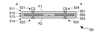
- FIG. 6 is a cross-sectional view taken along the line Aa in FIG.
- the detected portion 50 of the first embodiment includes a wiring pattern 511 of the first layer, a base material 551, a wiring pattern 512 of the second layer, a base material 552, a wiring pattern 513 of the third layer, and a base material.
- the 553 and the wiring pattern 514 of the fourth layer are laminated in this order. That is, in the detected portion 50, the wiring pattern and the base material are alternately arranged.
- the base materials 551, 552 and 553 are rectangular plate-shaped members formed of an insulating resin.
- the base materials 551 and 553 are prepregs obtained by impregnating, for example, a glass cloth with a resin such as epoxy and curing the prepreg, and the thickness is preferably 0.06 mm or more and 0.36 mm or less. Further, the base material 552 is a core material such as glass cloth, and the thickness is preferably 0.1 mm or more and 1.1 mm or less.
- the surface F1 of the detected portion 50 is a surface attached to the installation surface 122 of the key 12. Therefore, the width W of the detected unit 50 is smaller than the width W of one key 12. Further, the surface F2 is a surface opposite to the surface F1. Therefore, the surface F2 faces the signal generation unit 60.
- a plurality of vias C1 to C8 are provided in the detected unit 50.
- Vias C1 to C8 are circular contact holes penetrating the base materials 551, 552, and 553.
- the chip type capacitive element 52 is mounted on the terminal Na connected to the via C1 and the terminal Nb connected to the via C8. Specifically, one end of the capacitance element 52 is connected to the terminal Na, and the other end is connected to the terminal Nb.
- the first coil 51 of the detected portion 50 is composed of a wiring pattern 512 of the second layer and a wiring pattern 513 of the third layer. Specifically, the first coil 51 includes a first portion 521 and a fourth portion 524 formed in a spiral shape in the wiring pattern 512, and a second portion 522 formed in a spiral shape in the wiring pattern 513. It is composed of a third part 523.
- the center of the spiral in the first portion 521 and the center of the spiral in the second portion 522 is the via C3
- the center of the spiral in the third portion 523 and the center of the spiral in the fourth portion 524 is the via C6. Therefore, when viewed in a plan view from the signal generation unit 60, the first portion 521 and the second portion 522 overlap each other, and the third portion 523 and the fourth portion 524 overlap each other. Further, the first portion 521 and the fourth portion 524 are adjacent to each other along the longitudinal direction of the key 12 in the second layer. Similarly, the third portion 523 and the fourth portion 524 are adjacent to each other along the longitudinal direction of the key 12 in the third layer.
- the terminal Na is connected to one end (node N1) of the first portion 521 in the second layer via the via C1.
- the other end of the first portion 521 is connected to one end of the second portion 522 in the third layer via the via C3.
- the other end (node N2) of the second portion 522 is connected to one end (node N3) of the third portion 523 in the third layer.
- the other end of the third portion 523 is connected to one end of the fourth portion 524 in the second layer via the via C6.
- the other end (node N4) of the fourth portion 524 is connected to the terminal Nb of the first layer via the via C8.
- the first portion 521, the second portion 522, the third portion 523, and the fourth portion 524 are connected in series in this order when viewed from the terminal Na.
- the capacitance element 52 is mounted on the terminal Na and the terminal Nb, one end of the capacitance element 52 and one end of the first coil 51 are connected to each other, and the other end of the capacitance element 52 and the other end of the first coil 51 Are interconnected.
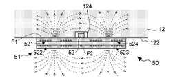
- a notch 124 is provided on the installation surface 122 of the key 12, as shown in FIG.
- the cutout portion 124 is a space recessed with respect to the installation surface 122.
- the cutout portion 124 is provided by cutting the installation surface 122 with, for example, a drill or the like.
- the capacitive element 52 projects from the surface F1 of the detected portion 50.
- the surface F1 of the detected portion 50 comes into contact with the installation surface 122 of the key 12.
- the capacitive element 52 is exposed before the detected portion 50 is installed on the installation surface 122, but the capacitive element 52 and the surface F1 are not exposed after the detected portion 50 is installed. Therefore, it is possible to prevent the capacitance element 52 from being damaged due to being caught by another member during maintenance of the keyboard instrument 100 or the like.
- the first coil 51 moves away from the second coil 61, the first coil 51 has the same direction as the magnetic field generated by the second coil 61 in the direction of preventing the magnetic field generated by the second coil 61 from decreasing.
- a directional magnetic field is generated. Therefore, in this case, a current is induced in the first coil 51 according to the magnetic field in the same direction as the magnetic field generated by the second coil 61.
- the first coil 51 of the detected unit 50 moves away from the second coil 61 in a state where the second coil 61 of the signal generation unit 60 generates a magnetic field in the direction shown in FIG.
- FIG. 7 a magnetic field in the same direction as the magnetic field generated by the second coil 61 is generated in the coil 51. Therefore, in FIG.
- the current flows counterclockwise in the first portion 521 and the second portion 522, and the current flows clockwise in the third portion 523 and the fourth portion 524. Therefore, in this case, the current flows in the route of terminal Na ⁇ via C1 ⁇ node N1 ⁇ via C3 ⁇ node N2 ⁇ node N3 ⁇ via C6 ⁇ node N4 ⁇ via C8 ⁇ terminal Nb.
- the magnetic field in the direction opposite to the magnetic field generated by the second coil 61 that is, FIG.
- the magnetic field shown in is generated in the first coil 51. Therefore, similarly, the current flows in the path of terminal Na ⁇ ... ⁇ terminal Nb.
- the first portion 521 and the second portion 522 of the first coil 51 are formed. The current flows clockwise, and the current flows counterclockwise in the third part 523 and the fourth part 524.
- the first portion 521 and the fourth portion 524 are spirally formed wiring patterns 512, and the second portion 522 and the third portion 523 are spirally formed.
- the first coil 51 is composed of a first portion 521, a second portion 522, a third portion 523, and a fourth portion 524 connected in series.
- This configuration has an advantage that the first coil 51 can be easily manufactured and handled as compared with a configuration in which the first coil 51 is formed by winding a conductive wire, for example. Further, it is easy to increase the inductance of the first coil 51 as compared with the case where the inductance of the first coil 51 is composed of only any portion. In other words, when the resonance frequency of the detected unit 50 is matched with the resonance frequency of the signal generation unit 60, the capacitance of the capacitive element 52 can be suppressed by the amount of increasing the inductance of the first coil 51.
- the first portion 521 and the fourth portion 524 of the first coil 51 are covered with the base material 551 and the base material 552. That is, the first portion 521 and the fourth portion 524 are formed between the base material 551 and the base material 552.
- the second portion 522 and the third portion 523 are covered with the base material 552 and the base material 553. That is, the second portion 522 and the third portion 523 are formed between the base material 552 and the base material 553. Therefore, the first coil 51 is protected by at least the base material 551 and the base material 553 functioning as protective members. That is, the first coil 51 facing the second coil 61 of the signal generation unit 60 is not exposed in the detected unit 50.
- the base material 551 functions as an example of the first insulating layer
- the wiring pattern 512 functions as an example of the first wiring pattern
- the base material 552 functions as an example of the second insulating layer.
- the wiring pattern 513 functions as an example of the second wiring pattern
- the base material 553 functions as an example of the third insulating layer. Further, the base material 551 and the base material 553 function as an example of the protective member.
- the detected portion 50 in the second embodiment is composed of a substrate including a two-layer wiring pattern.
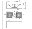
- FIG. 11 is a plan view showing the wiring patterns of the first layer and the second layer in the detected unit 50 in a state of being seen through from the signal generation unit 60. Note that in FIG. 11, the illustration of the capacitance element 52 is omitted for convenience. Further, FIG. 12 is a cross-sectional view taken along the line CC in FIG.
- the detected portion 50 of the second embodiment is a laminate in which the wiring pattern 511 of the first layer, the base material 551, the wiring pattern 512 of the second layer, and the base material 552 are laminated in this order. That is, in the detected portion 50 of the second embodiment, the wiring pattern 513 of the third layer, the base material 553, and the wiring pattern 514 of the fourth layer are omitted as compared with the first embodiment.
- Vias C1, C3, C6 and C8 are provided in the detected unit 50. These vias C1, C3, C6 and C8 are contact holes.
- the capacitance element 52 is mounted in the region A1 including the terminal Na connected to the via C1 and the terminal Nb connected to the via C8.
- the first coil 51 of the detected portion 50 is configured by the wiring pattern 512 of the second layer.
- the first coil 51 is composed of a first portion 521 formed in a spiral shape and a second portion 522 formed in a spiral shape in the same direction in the wiring pattern 512.
- the center of the spiral in the first portion 521 is the via C3
- the center of the spiral in the second portion 522 is the via C6.
- the via C3 and the via C6 are connected to each other via the wiring 515 which is a part of the wiring pattern 511.
- the terminal Na in the region A1 is connected to one end (node N21) of the first portion 521 in the second layer via the via C1.
- the other end of the first portion 521 is connected to the via C6 via the via C3 and the wiring 515 in the first layer.
- the wiring 515 is connected to the second portion 522 in the second layer via the via C6.
- the other end (node N22) of the second portion 522 is connected to the terminal Nb in the first layer via the via C8.
- the first portion 521 and the second portion 522 are connected in series.
- the total number of parts constituting the first coil 51 is halved as compared with the first embodiment, but the direction in which the magnetic field is generated is the same as that in the first embodiment. That is, magnetic fields in opposite directions are generated in the first portion 521 and the second portion 522. Since the plurality of keys 12 on the keyboard 10 are arranged in the direction perpendicular to the paper surface of FIG. 12, the diffusion of the magnetic field between the keys 12 adjacent to each other is reduced. Therefore, it is possible to generate a detection signal D that accurately reflects each position Z of the plurality of keys 12.
- the first portion 521 and the second portion 522 constituting the first coil 51 are covered with the base material 551 and the base material 552, so that they are not exposed. That is, in the second embodiment, the base material 551 and the base material 552 function as protective members, so that the first coil 51 is protected. Therefore, also in the second embodiment, damage to the first coil 51 due to rubbing by a tool or the like is prevented. Further, in the second embodiment, as compared with the first embodiment, the wiring pattern 513 of the third layer, the base material 553, and the wiring pattern 514 of the fourth layer do not exist, so that the configuration becomes simpler accordingly.
- the base material 551 functions as an example of the first insulating layer
- the wiring pattern 512 functions as an example of the first wiring pattern
- the base material 552 functions as an example of the second insulating layer.
- the base material 551 and the base material 552 function as an example of the protective member.
- the detected portion 50 in the third embodiment is composed of a substrate including four layers of wiring patterns as in the first embodiment.
- FIG. 13 is a plan view showing the wiring patterns of the first layer and the second layer in the detected unit 50 in a state of being seen through from the signal generation unit 60. Note that in FIG. 13, the illustration of the capacitance element 52 is omitted for convenience.
- the detected portion 50 of the third embodiment has a wiring pattern 511 of the first layer, a base material 551, a wiring pattern 512 of the second layer, and a base material 552.
- the wiring pattern 513 of the third layer, the base material 553, and the wiring pattern 514 of the fourth layer are laminated in this order.
- the first coil 51 of the detected portion 50 is composed of the first portion 521 of the wiring pattern 512 of the second layer and the second portion 522 of the wiring pattern 513 of the third layer. ..
- the first portion 521 is formed in a spiral shape.
- the second portion 522 is formed in a spiral shape in the direction opposite to that of the first portion 521.
- the center of the spiral in the first portion 521 and the center of the spiral in the second portion 522 are vias C3. That is, in the third embodiment, the first portion 521 and the second portion 522 are connected to each other via the via C3.
- the terminal Na in the region A1 is connected to one end (node N31) of the first portion 521 in the second layer via the via C1.
- the other end of the first portion 521 is connected to one end of the second portion 522 in the third layer via the via C3.
- the other end (node N32) of the second portion 522 is connected to the terminal Nb in the region A1 in the first layer via the via C8.
- the structure of the detected portion 50 of the third embodiment can be sufficiently inferred from FIG. 6, which is a cross-sectional view of the first embodiment, and thus the illustration is omitted.
- the second portion 522 constituting the first coil 51 is covered with the base material 552 and the base material 553, so that the first coil 51 is not exposed. That is, in the third embodiment, the base material 552 and the base material 553 function as protective members, so that the first coil 51 is protected. Therefore, also in the third embodiment, damage to the first coil 51 due to rubbing by a tool or the like is prevented. Further, in the third embodiment, the portion constituting the first coil 51 is halved as compared with the first embodiment, but the first portion 521 and the second portion 522 are positioned so as to overlap each other and the magnetic field. Occurs in the same direction. Therefore, the substrate area of the third embodiment is about half that of the first embodiment.
- the base material 551 functions as an example of the first insulating layer
- the wiring pattern 512 functions as an example of the first wiring pattern
- the base material 552 functions as an example of the second insulating layer.
- the wiring pattern 513 functions as an example of the second wiring pattern
- the base material 553 functions as an example of the third insulating layer.
- the base material 552 and the base material 553 function as an example of the protective member.
- FIG. 14 is a plan view showing the wiring pattern in the detected unit 50 in a see-through state when viewed from the signal generating unit 60.
- the first coil 51 of the detected portion 50 in the fourth embodiment is composed of either the first portion 521 or the second portion 522. That is, the detected unit 50 is switched from one of the state in which the first coil 51 is composed of the first portion 521 and the state in which the first coil 51 is composed of the second portion 522 to the other.
- a jumper switch 560 is provided on the surface of the first layer.
- the jumper switch 560 is a switch that connects either the via C21 or the via C22 to the terminal Na in the region A1. Specifically, when connecting the terminal Na to the via C21, the socket is inserted as shown in the right column in the figure, and when connecting the terminal Na to the via C22, as shown in the left column in the figure. The socket is plugged into.
- the terminal Na is connected to one end (node N41) of the first portion 521 in the second layer via the via C21.
- the terminal Na is connected to one end (node N42) of the second portion 522 in the third layer via the via C22.
- the other end of the first portion 521 and the other end of the second portion 522 are connected to the terminal Nb in the region A1 in the first layer via the common via C3.
- the jumper switch 560 in the initial initial state in which the detected portion 50 is installed, the jumper switch 560 is positioned as shown in the left column, and the second portion 522 functions as the first coil 51.
- the jumper switch 560 if any trouble occurs in the second part 522, the jumper switch 560 is switched to the state shown in the right column, and the first part 521 functions as the first coil 51. That is, in the fourth embodiment, while the first portion 521 is used as a spare coil and the second portion 522 functions as the first coil 51, if a problem occurs in the second portion 522, the jumper switch 560 is switched.
- the first portion 521 can function as the first coil 51.
- the displacement sensor 20 of the fourth embodiment includes a detected portion 50 installed on a key 12, which is an example of a movable member, and a second coil 61 that generates a magnetic field by supplying an electric current. It includes a signal generation unit 60 including the signal generation unit 60.
- the detected portion 50 includes a first portion 521 protected by a protective member (base material 551 or base material 552) formed of an insulating resin, and a second portion 522 which is an example of the third coil.
- the jumper switch 560 functions as a switching unit for switching between a first state in which the first portion 521 constitutes a resonance circuit and a second state in which the second portion 522 constitutes a resonance circuit.
- the signal generation unit 60 generates a detection signal according to the relative position between the resonance circuit of the detected unit 50 and the second coil 61.
- the second portion 522 may or may not be protected by a protective member.
- the fourth embodiment there may be no member covering the second portion 522, and even if the second portion 522 is damaged, if the jumper switch 560 is switched, the first portion 521 functions as the first coil 51. be able to. That is, in the fourth embodiment, when the first portion 521 functions as the first coil 51 by the jumper switch 560, the base material 552 functions as a protective member, so that the first coil 51 is protected.
- the base material 551 functions as an example of the first insulating layer
- the wiring pattern 512 functions as an example of the first wiring pattern
- the base material 552 functions as an example of the second insulating layer.
- the wiring pattern 513 functions as an example of the second wiring pattern
- the base material 553 functions as an example of the third insulating layer.
- FIG. 15 is a schematic diagram of a configuration in which the displacement sensor 20 is applied to the string striking mechanism 91 of the keyboard instrument 100.
- the string striking mechanism 91 is an action mechanism that strikes a string (not shown) in conjunction with the displacement of each key 12 of the keyboard 10.
- the string striking mechanism 91 includes a hammer 911 capable of striking a string by rotation and a transmission mechanism 912 (for example, a wipen, a jack, a repetition lever, etc.) that rotates the hammer 911 in conjunction with the displacement of the key 12. Is provided for each key 12.
- the detected portion 50 is installed on a hammer 911 (for example, a hammer shank).
- the signal generation unit 60 is installed on the support member 913.
- the displacement sensor 20 detects the displacement of the hammer 911.
- the support member 913 is a structure that supports, for example, the string striking mechanism 91.
- the detected portion 50 may be installed on a movable member other than the hammer 911 in the string striking mechanism 91.
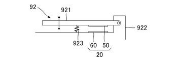
- FIG. 16 is a schematic diagram of a configuration in which the displacement sensor 20 is applied to the pedal mechanism 92 of the keyboard instrument 100.
- the pedal mechanism 92 includes a pedal 921 operated by the user with his / her foot, a support member 922 that supports the pedal 921, and an elastic body 923 that urges the pedal 921 upward in the vertical direction.
- the detected portion 50 is installed on the bottom surface of the pedal 921.
- the signal generation unit 60 is installed on the support member 922 so as to face the detected unit 50.
- the displacement sensor 20 detects the displacement of the pedal 921.
- the musical instrument in which the pedal mechanism 92 is used is not limited to the keyboard instrument 100.
- a pedal mechanism 92 having the same configuration is used for any musical instrument such as a percussion instrument.
- the object of detection by the displacement sensor is comprehensively expressed as a movable member that is displaced according to the playing motion.
- the movable member includes a performance operator such as a key 12 or a pedal 921 directly operated by the user, and a structure such as a hammer 911 that is displaced in conjunction with an operation on the performance operator.
- the movable member in the present disclosure is not limited to the member that is displaced according to the playing motion. That is, the movable member is comprehensively expressed as a displaceable member regardless of the trigger for causing the displacement.
- the configuration in which the capacitance element 52 on the surface F1 is connected to the wiring pattern 511 formed on the surface F1 of the detected portion 50 is illustrated, but the wiring pattern (512 or 512 or) between the insulating layers is illustrated.
- the capacitive element 52 on the surface F1 may be connected to 513) by, for example, a blind via.
- the wiring pattern 511 may be omitted from the detected portion 50. That is, it is assumed that the wiring pattern 511 does not exist on the surface F1 of the detected portion 50.
- the base material (552, 553) is exemplified as the protective member, but the form of the protective member is not limited to the above examples.
- an insulating layer formed on the surface of a flat plate-shaped base material may be used as a “protective member”.
- the insulating layer is, for example, a film body for the purpose of waterproofing, and is formed of an insulating material such as silicon, epoxy, or urethane.
- Various processing techniques such as coating or potting are used to form the insulating layer.
- the "protective member” is a concept that includes not only an independent base material but also a film body that covers the surface of the base material.
- the configuration in which the keyboard instrument 100 includes the sound source circuit 34 is illustrated.
- the sound source circuit 34 is used. It may be omitted.
- the detection system 15 is used to record the performance content of the keyboard instrument 100.
- the sound generation mechanism and the sound source circuit 34 are comprehensively expressed as a sound generation unit that generates sound according to the result of detection by the detection system 15.
- the present disclosure is also specified as a device (performance operation device) that controls a musical sound by outputting an operation signal according to a performance operation to the sound source circuit 34 or a sounding mechanism.
- the device not having the sound source circuit 34 or the sounding mechanism for example, the MIDI controller or the pedal mechanism 92 described above. It is included in the concept of instrument playing apparatus. That is, the performance operation device in the present disclosure is comprehensively expressed as a device operated by a performer (operator) for performance.
- the entire surface is covered with a resin layer, but the entire surface may not necessarily be covered.
- the protective member may be covered with a net-like member in the pattern.
- the prismatic members may be arranged side by side at predetermined intervals or without leaving a space between the members in the longitudinal direction or the lateral direction of the substrate. Further, only the portion of the coil pattern may be covered with the protective member.
- the displacement sensor according to the aspect (first aspect) of the present disclosure is a displacement sensor that detects the displacement of the movable member in response to an operation, and is installed on the movable member and protected by a protective member formed of an insulating resin. Detection according to the relative position of the first coil of the detected portion and the second coil facing the first coil of the detected portion, including the detected portion including the first coil and the second coil that generates a magnetic field by supplying a current. It includes a signal generation unit that generates a signal. According to this aspect, since the first coil is protected by the protective member, it is possible to prevent the first coil from being damaged by rubbing or the like.
- the distance between the first coil and the second coil in the direction of the central axis of the second coil changes according to the displacement of the movable member.
- the detected portion and the second coil move relatively in a plane perpendicular to the central axis of the second coil (that is, the detected portion and the second coil in the direction of the central axis of the second coil).
- the level of the detection signal can be significantly changed with respect to the displacement of the movable member.
- the detected portion includes a capacitive element connected to the first coil. According to this aspect, there is an advantage that the resonance frequency of the first coil and the capacitive element can be adjusted according to the capacitance of the capacitive element.
- the movable member has an installation surface on which the detected portion is installed, the installation surface is provided with a notch, and the capacitive element is provided in the notch.
- the detected portion is installed on the movable member.
- the detected portion includes at least a first insulating layer, a first wiring pattern, and a second insulating layer, and the first wiring pattern is the said.
- the first coil is a spiral-shaped portion included in the first wiring pattern.
- the detected portion includes at least the first insulating layer, the first wiring pattern, the second insulating layer, the second wiring pattern, and the third insulating layer. Including, the first wiring pattern is located between the first insulating layer and the second insulating layer, and the second wiring pattern is located between the second insulating layer and the third insulating layer.
- the first coil includes a first portion, a second portion, a third portion, and a fourth portion, and the first portion and the fourth portion are spiral-shaped portions included in the first wiring pattern.
- the second portion and the third portion are spiral-shaped portions included in the second wiring pattern, and the first portion and the second portion overlap each other in a plan view, and the third portion and the third portion.
- the fourth portion and the fourth portion overlap each other in a plan view, and the magnetic field generated by the first portion and the magnetic field generated by the second portion are in the first direction, and the magnetic field generated by the third portion. And the magnetic field generated by the fourth portion are the second direction opposite to the first direction.
- a magnetic field in the first direction is generated in the first portion and the second portion, and a magnetic field in the direction opposite to the first direction is generated in the third portion and the fourth portion.
- the diffusion of the magnetic field to the surroundings is reduced. Therefore, in a configuration in which a plurality of first coils corresponding to different movable members are close to each other, it is possible to generate a detection signal that reflects the displacement of each of the plurality of movable members with high accuracy.
- planar view means observing along the direction perpendicular to the surface of the wiring pattern, or observing from the direction perpendicular to the surface of the insulating layer. Observing along the axial direction of the first coil may be expressed as "plan view”.
- the detected portion includes at least a first insulating layer, a first wiring pattern, and a second insulating layer, and the first wiring pattern is the said.
- the first coil Located between the first insulating layer and the second insulating layer, the first coil includes a first portion and a second portion, and the first portion and the second portion are in the first wiring pattern. It is a spiral-shaped portion included, and the magnetic field generated by the first portion and the magnetic field generated by the second portion are opposite to each other. According to this aspect, since the first portion and the second portion overlap in a plan view and the generated magnetic fields are in the same direction, the strength of the magnetic field is increased as compared with the single unit of the first portion or the second portion. be able to.
- the detected portion includes at least the first insulating layer, the first wiring pattern, the second insulating layer, the second wiring pattern, and the third insulating layer. Including, the first wiring pattern is located between the first insulating layer and the second insulating layer, and the second wiring pattern is located between the second insulating layer and the third insulating layer.
- the first coil includes a first portion and a second portion, the first portion is a spiral-shaped portion included in the first wiring pattern, and the second portion is included in the second wiring pattern. It is a spiral-shaped portion included, and the first portion and the second portion overlap each other in a plan view, and the magnetic field generated by the first portion and the magnetic field generated by the second portion mutually overlap. In the same direction. According to this aspect, since the first portion and the second portion overlap in a plan view, the space required for installing the detected portion is reduced.
- the detected portion resonates with the third coil, the first state in which the first coil constitutes a resonance circuit, and the third coil. Includes a switching unit that switches between the second state that constitutes the circuit. According to this aspect, even if the other coil is damaged, the other coil can be used by replacing it with the first coil protected by the protective member.
- the performance operation device generates the displacement sensor according to any one of the first to ninth aspects and an acoustic signal representing a sound according to the level of the detection signal. It is equipped with a sound control unit.
- 100 keyboard instrument (playing operation device), 10 ... keyboard, 12 ... key, 15 ... detection system, 20 ... displacement sensor, 21 ... signal processing circuit, 22 ... supply circuit, 23 ... output circuit, 30 ... information processing device, 50 ... Detected part, 51 ... 1st coil, 52 ... Capacitive element, 521 ... 1st part, 522 ... 2nd part, 523 ... 3rd part, 524 ... 4th part, 551, 552, 535 ... Base material.
Landscapes
- Physics & Mathematics (AREA)
- General Physics & Mathematics (AREA)
- Engineering & Computer Science (AREA)
- Acoustics & Sound (AREA)
- Multimedia (AREA)
- Measurement Of Length, Angles, Or The Like Using Electric Or Magnetic Means (AREA)
- Electrophonic Musical Instruments (AREA)
Priority Applications (2)
| Application Number | Priority Date | Filing Date | Title |
|---|---|---|---|
| CN202190000320.0U CN218297031U (zh) | 2020-03-12 | 2021-03-08 | 位移传感器及演奏操作装置 |
| JP2022507186A JP7327646B2 (ja) | 2020-03-12 | 2021-03-08 | 変位センサーおよび演奏操作装置 |
Applications Claiming Priority (2)
| Application Number | Priority Date | Filing Date | Title |
|---|---|---|---|
| JP2020042520 | 2020-03-12 | ||
| JP2020-042520 | 2020-03-12 |
Publications (1)
| Publication Number | Publication Date |
|---|---|
| WO2021182409A1 true WO2021182409A1 (ja) | 2021-09-16 |
Family
ID=77670885
Family Applications (1)
| Application Number | Title | Priority Date | Filing Date |
|---|---|---|---|
| PCT/JP2021/009027 Ceased WO2021182409A1 (ja) | 2020-03-12 | 2021-03-08 | 変位センサーおよび演奏操作装置 |
Country Status (3)
| Country | Link |
|---|---|
| JP (1) | JP7327646B2 (https=) |
| CN (1) | CN218297031U (https=) |
| WO (1) | WO2021182409A1 (https=) |
Cited By (2)
| Publication number | Priority date | Publication date | Assignee | Title |
|---|---|---|---|---|
| US20220246122A1 (en) * | 2017-12-20 | 2022-08-04 | Sonuus Limited | Keyboard sensor systems and methods |
| US20220277717A1 (en) * | 2019-11-20 | 2022-09-01 | Yamaha Corporation | Detection system, musical instrument playing apparatus, and musical keyboard instrument |
Families Citing this family (1)
| Publication number | Priority date | Publication date | Assignee | Title |
|---|---|---|---|---|
| JP7302739B2 (ja) * | 2020-03-26 | 2023-07-04 | ヤマハ株式会社 | 変位センサーおよび電子楽器 |
Citations (4)
| Publication number | Priority date | Publication date | Assignee | Title |
|---|---|---|---|---|
| JP2000149211A (ja) * | 1998-05-07 | 2000-05-30 | Canon Inc | 磁気ヘッド用平面コイル部品、光磁気記録用磁気ヘッドおよび光磁気記録装置 |
| JP2002110422A (ja) * | 2000-09-28 | 2002-04-12 | Murata Mfg Co Ltd | チップ型コイル部品 |
| JP2010122012A (ja) * | 2008-11-18 | 2010-06-03 | Jtekt Corp | 基板形複層コイル及び変位センサ装置 |
| WO2019122867A1 (en) * | 2017-12-20 | 2019-06-27 | Sonuus Limited | Keyboard sensor systems and methods |
-
2021
- 2021-03-08 JP JP2022507186A patent/JP7327646B2/ja active Active
- 2021-03-08 WO PCT/JP2021/009027 patent/WO2021182409A1/ja not_active Ceased
- 2021-03-08 CN CN202190000320.0U patent/CN218297031U/zh active Active
Patent Citations (4)
| Publication number | Priority date | Publication date | Assignee | Title |
|---|---|---|---|---|
| JP2000149211A (ja) * | 1998-05-07 | 2000-05-30 | Canon Inc | 磁気ヘッド用平面コイル部品、光磁気記録用磁気ヘッドおよび光磁気記録装置 |
| JP2002110422A (ja) * | 2000-09-28 | 2002-04-12 | Murata Mfg Co Ltd | チップ型コイル部品 |
| JP2010122012A (ja) * | 2008-11-18 | 2010-06-03 | Jtekt Corp | 基板形複層コイル及び変位センサ装置 |
| WO2019122867A1 (en) * | 2017-12-20 | 2019-06-27 | Sonuus Limited | Keyboard sensor systems and methods |
Cited By (3)
| Publication number | Priority date | Publication date | Assignee | Title |
|---|---|---|---|---|
| US20220246122A1 (en) * | 2017-12-20 | 2022-08-04 | Sonuus Limited | Keyboard sensor systems and methods |
| US12112732B2 (en) * | 2017-12-20 | 2024-10-08 | Sonuus Limited | Keyboard sensor systems and methods |
| US20220277717A1 (en) * | 2019-11-20 | 2022-09-01 | Yamaha Corporation | Detection system, musical instrument playing apparatus, and musical keyboard instrument |
Also Published As
| Publication number | Publication date |
|---|---|
| JP7327646B2 (ja) | 2023-08-16 |
| CN218297031U (zh) | 2023-01-13 |
| JPWO2021182409A1 (https=) | 2021-09-16 |
Similar Documents
| Publication | Publication Date | Title |
|---|---|---|
| JP7683769B2 (ja) | 演奏操作装置 | |
| WO2021182409A1 (ja) | 変位センサーおよび演奏操作装置 | |
| JP7622773B2 (ja) | 変位センサーおよび電子楽器 | |
| US20220277717A1 (en) | Detection system, musical instrument playing apparatus, and musical keyboard instrument | |
| US20220277719A1 (en) | Musical instrument playing apparatus and musical keyboard instrument | |
| JP2022060655A (ja) | 回路基板および検出システム | |
| JP2025061927A (ja) | 検出システムおよび鍵盤装置 | |
| US20250078794A1 (en) | Detection system and musical instrument | |
| JP2025129285A (ja) | 楽器用検出システムおよび楽器 | |
| JP2025005601A (ja) | 検出システムおよび楽器 | |
| JP7800303B2 (ja) | 検出システムおよび楽器 |
Legal Events
| Date | Code | Title | Description |
|---|---|---|---|
| 121 | Ep: the epo has been informed by wipo that ep was designated in this application |
Ref document number: 21767567 Country of ref document: EP Kind code of ref document: A1 |
|
| ENP | Entry into the national phase |
Ref document number: 2022507186 Country of ref document: JP Kind code of ref document: A |
|
| NENP | Non-entry into the national phase |
Ref country code: DE |
|
| 122 | Ep: pct application non-entry in european phase |
Ref document number: 21767567 Country of ref document: EP Kind code of ref document: A1 |