WO2021181883A1 - 異物検出装置 - Google Patents
異物検出装置 Download PDFInfo
- Publication number
- WO2021181883A1 WO2021181883A1 PCT/JP2021/001507 JP2021001507W WO2021181883A1 WO 2021181883 A1 WO2021181883 A1 WO 2021181883A1 JP 2021001507 W JP2021001507 W JP 2021001507W WO 2021181883 A1 WO2021181883 A1 WO 2021181883A1
- Authority
- WO
- WIPO (PCT)
- Prior art keywords
- coil
- detection
- power
- foreign matter
- circuit
- Prior art date
- Legal status (The legal status is an assumption and is not a legal conclusion. Google has not performed a legal analysis and makes no representation as to the accuracy of the status listed.)
- Ceased
Links
Images

Classifications
-
- H—ELECTRICITY
- H02—GENERATION; CONVERSION OR DISTRIBUTION OF ELECTRIC POWER
- H02J—ELECTRIC POWER NETWORKS; CIRCUIT ARRANGEMENTS OR SYSTEMS FOR SUPPLYING OR DISTRIBUTING ELECTRIC POWER; SYSTEMS FOR STORING ELECTRIC ENERGY
- H02J50/00—Circuit arrangements or systems for wireless supply or distribution of electric power
- H02J50/60—Circuit arrangements or systems for wireless supply or distribution of electric power responsive to the presence of foreign objects, e.g. detection of living beings
-
- H—ELECTRICITY
- H02—GENERATION; CONVERSION OR DISTRIBUTION OF ELECTRIC POWER
- H02J—ELECTRIC POWER NETWORKS; CIRCUIT ARRANGEMENTS OR SYSTEMS FOR SUPPLYING OR DISTRIBUTING ELECTRIC POWER; SYSTEMS FOR STORING ELECTRIC ENERGY
- H02J50/00—Circuit arrangements or systems for wireless supply or distribution of electric power
- H02J50/005—Mechanical details of housing or structure aiming to accommodate the power transfer means, e.g. mechanical integration of coils, antennas or transducers into emitting or receiving devices
-
- H—ELECTRICITY
- H02—GENERATION; CONVERSION OR DISTRIBUTION OF ELECTRIC POWER
- H02J—ELECTRIC POWER NETWORKS; CIRCUIT ARRANGEMENTS OR SYSTEMS FOR SUPPLYING OR DISTRIBUTING ELECTRIC POWER; SYSTEMS FOR STORING ELECTRIC ENERGY
- H02J50/00—Circuit arrangements or systems for wireless supply or distribution of electric power
- H02J50/10—Circuit arrangements or systems for wireless supply or distribution of electric power using inductive coupling
- H02J50/12—Circuit arrangements or systems for wireless supply or distribution of electric power using inductive coupling of the resonant type
-
- H—ELECTRICITY
- H02—GENERATION; CONVERSION OR DISTRIBUTION OF ELECTRIC POWER
- H02J—ELECTRIC POWER NETWORKS; CIRCUIT ARRANGEMENTS OR SYSTEMS FOR SUPPLYING OR DISTRIBUTING ELECTRIC POWER; SYSTEMS FOR STORING ELECTRIC ENERGY
- H02J50/00—Circuit arrangements or systems for wireless supply or distribution of electric power
- H02J50/40—Circuit arrangements or systems for wireless supply or distribution of electric power using two or more transmitting or receiving devices
- H02J50/402—Circuit arrangements or systems for wireless supply or distribution of electric power using two or more transmitting or receiving devices the two or more transmitting or the two or more receiving devices being integrated in the same unit, e.g. power mats with several coils or antennas with several sub-antennas
-
- Y—GENERAL TAGGING OF NEW TECHNOLOGICAL DEVELOPMENTS; GENERAL TAGGING OF CROSS-SECTIONAL TECHNOLOGIES SPANNING OVER SEVERAL SECTIONS OF THE IPC; TECHNICAL SUBJECTS COVERED BY FORMER USPC CROSS-REFERENCE ART COLLECTIONS [XRACs] AND DIGESTS
- Y02—TECHNOLOGIES OR APPLICATIONS FOR MITIGATION OR ADAPTATION AGAINST CLIMATE CHANGE
- Y02T—CLIMATE CHANGE MITIGATION TECHNOLOGIES RELATED TO TRANSPORTATION
- Y02T10/00—Road transport of goods or passengers
- Y02T10/60—Other road transportation technologies with climate change mitigation effect
- Y02T10/70—Energy storage systems for electromobility, e.g. batteries
-
- Y—GENERAL TAGGING OF NEW TECHNOLOGICAL DEVELOPMENTS; GENERAL TAGGING OF CROSS-SECTIONAL TECHNOLOGIES SPANNING OVER SEVERAL SECTIONS OF THE IPC; TECHNICAL SUBJECTS COVERED BY FORMER USPC CROSS-REFERENCE ART COLLECTIONS [XRACs] AND DIGESTS
- Y02—TECHNOLOGIES OR APPLICATIONS FOR MITIGATION OR ADAPTATION AGAINST CLIMATE CHANGE
- Y02T—CLIMATE CHANGE MITIGATION TECHNOLOGIES RELATED TO TRANSPORTATION
- Y02T10/00—Road transport of goods or passengers
- Y02T10/60—Other road transportation technologies with climate change mitigation effect
- Y02T10/7072—Electromobility specific charging systems or methods for batteries, ultracapacitors, supercapacitors or double-layer capacitors
Definitions
- the present invention relates to a foreign matter detecting device that detects foreign matter in a power transmission system in which electric power is transmitted in a non-contact manner.
- non-contact power supply also called wireless power supply
- a method of feeding power by electromagnetic induction is known.
- the coil on the primary side (transmission side or power supply side) hereinafter referred to as the transmission coil
- the coil on the secondary side (power reception side) hereinafter referred to as the reception coil
- the non-contact power supply device determines that some foreign matter has been mixed between the transmitting coil and the receiving coil of the power receiving device, and stops the power supply to the transmitting coil.
- the power transmission characteristic from the power transmitting device to the receiving device does not change, and as a result, the foreign substance mixed between the transmitting coil and the receiving coil is mixed. May not be detected.
- an object of the present invention is to provide a foreign matter detecting device capable of improving the detection accuracy of foreign matter mixed between the transmitting coil of the power transmitting side device and the receiving coil of the power receiving side device.
- a foreign matter detecting device includes a plurality of detection coils arranged at different positions between the transmission coil of the power transmission device and the reception coil of the power reception device, and each of the plurality of detection coils, in which power is transmitted in a non-contact manner.
- a plurality of capacitors forming a resonance circuit together with the detection coil, a feeding coil arranged so as to be electromagnetically coupled to each of the plurality of detection coils, and a predetermined frequency of each of the plurality of detection coils via the feeding coil.
- the voltage output for the supplied AC power is detected from each of the power supply circuit that supplies AC power and the plurality of detection coils, and between the transmit coil and the receive coil according to the detected voltage.
- the foreign matter detecting device can improve the detection accuracy of foreign matter mixed between the transmitting coil of the power transmitting side device and the receiving coil of the power receiving side device.
- the detection circuit has a storage unit for storing the reference voltage output from the detection coil when there is no foreign matter mixed between the transmission coil and the reception coil for each of the plurality of detection coils.
- the ratio of the voltage detected for the detection coil to the reference voltage of the detection coil is out of the range of the predetermined allowable voltage change rate, the distance between the transmission coil and the reception coil is reached. It is preferable to determine that there is a foreign substance mixed in the coil.
- the foreign matter detecting device can determine the presence or absence of foreign matter by using the same allowable voltage change rate regardless of the relative positional relationship between each detection coil and the feeding coil. , Foreign matter can be detected accurately regardless of the position where foreign matter is mixed, and it is not necessary to set the judgment standard for foreign matter mixing for each detection coil, so that the complexity of setting the judgment standard for foreign matter mixing can be reduced. ..
- the foreign matter detection device can prevent the AC power for detecting foreign matter from affecting the power transmission from the power transmission device to the power receiving device, and the power transmitted from the power transmission device to the power receiving device is received by the transmission coil. It is possible to prevent the detection of foreign matter mixed between the coils from being affected, and to detect the foreign matter with high accuracy.
- the feeding coil is arranged so as to surround the plurality of detection coils when viewed from the central axis direction of the transmitting coil. Therefore, the foreign matter detecting device can surely supply the electric power used for detecting the foreign matter to each of the plurality of detection coils.
- the size of each of the plurality of detection coils seen from the central axis direction of the transmitting coil is smaller than the size seen from the central axis direction of the transmitting coil.
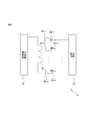
- FIG. 1 is a schematic configuration diagram of a power transmission system including a foreign matter detecting device according to an embodiment of the present invention.
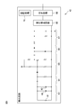
- FIG. 2 is a schematic configuration diagram of a foreign matter detecting device.
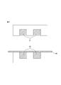
- FIG. 3 is a schematic side sectional view showing an example of the positional relationship between the substrate on which the foreign matter detection device is provided and the transmission coil.
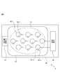
- FIG. 4 is a schematic plan view showing an example of arrangement of a plurality of detection coils and a feeding coil included in the foreign matter detection device.
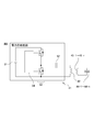
- FIG. 5 is a circuit configuration diagram showing an example of a power supply circuit.
- FIG. 6 is a circuit configuration diagram showing an example of a detection circuit.
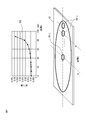
- FIG. 7 is a diagram for explaining the relationship between the positional relationship between the feeding coil and the detection coil and the degree of coupling.
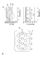
- FIG. 8 is a diagram showing a measurement result showing the relationship between the position of the mixed foreign matter, the voltage output from each detection coil, and the voltage change rate.
- This foreign matter detection device includes a transmission coil of a power transmission side device (hereinafter, simply referred to as a power transmission device) and a power reception side device (hereinafter, simply referred to as a power reception device) of a power transmission system that transmits power by non-contact. It has a substrate arranged between the receiving coil and the feeding coil formed on the substrate for supplying power for detecting foreign matter, and the feeding coil arranged at different positions in the feeding coil. It has a plurality of detection coils that can be electromagnetically coupled to and are smaller than the power feeding coil.
- Each of the plurality of detection coils is different from the frequency of the power supplied to the transmission coil of the transmission device, and is a resonance circuit including the transmission coil (when a resonance circuit is provided on the transmission side) and a resonance circuit including the reception coil. It is possible to resonate at a frequency at which none of the above resonates.
- This foreign matter detection device supplies AC power having a frequency at which the detection coils resonate to the feeding coils, while detecting the voltage output from each of the plurality of detection coils.
- the resonance characteristic of any one of the plurality of detection coils changes, and as a result, the detected voltage changes.
- this foreign matter detecting device monitors the detected voltage, and when the voltage deviates from a predetermined reference range corresponding to the case where foreign matter is not mixed, foreign matter is mixed between the transmitting coil and the receiving coil. It is determined that it has been done. Further, this foreign matter detection device is a reference voltage for each detection coil based on the voltage output from each detection coil when power is supplied to the power feeding coil in the absence of foreign matter (hereinafter, simply referred to as a reference voltage). ) Is set, and the permissible voltage change rate with respect to the ratio of the detected voltage to the reference voltage is set as the reference range to suppress erroneous detection of foreign matter due to the difference in the positional relationship between each detection coil and the feeding coil. do.
- FIG. 1 is a schematic configuration diagram of a power transmission system including a foreign matter detecting device according to one embodiment of the present invention.
- the power transmission system 1 includes a power transmission device 2, a power receiving device 3, and a foreign matter detecting device 4.
- the power transmitting device 2 and the power receiving device 3 form a non-contact power feeding device, and electric power is transmitted from the power transmitting device 2 to the power receiving device 3 in a non-contact manner via a space.
- the power transmission device 2 has a power supply circuit 11 and a transmission coil 12.
- the power receiving device 3 has a receiving coil 21, a resonance capacitor 22, and a power receiving circuit 23.
- the power transmission system 1 can be, for example, a so-called primary series secondary series resonant capacitor system (SS system) or a primary series secondary parallel resonant capacitor system (SP system) non-contact power feeding device.
- SS system primary series secondary series resonant capacitor system
- SP system primary series secondary parallel resonant capacitor system
- the power transmission system 1 does not utilize the resonance on the primary side and the receiving coil and the resonance capacitor resonate in series on the secondary side (NS method), or does not utilize the resonance on the primary side and is secondary.
- a non-contact power feeding device of a method (NP method) in which the receiving coil and the resonance capacitor resonate in parallel on the side may be used.
- the power supply circuit 11 supplies AC power to the transmission coil 12. Therefore, the power supply circuit 11 controls, for example, a DC power supply that supplies DC power, an inverter circuit that converts DC power supplied from the DC power supply into AC power and supplies it to the transmission coil 12, and an inverter circuit. It has a control circuit.
- the inverter circuit may be a full-bridge inverter in which four switching elements (for example, MOSFETs) are connected in a full-bridge shape, or a half-bridge inverter in which two switching elements are connected in a half-bridge shape. There may be.
- the control circuit turns on / off each switching element of the inverter circuit so that the frequency of the AC power supplied to the transmission coil 12 becomes a predetermined frequency (for example, the frequency at which the resonance circuit of the power receiving device 3 resonates). Control switching.
- the power supply circuit 11 may further have a DC-DC converter between the DC power supply and the inverter circuit.
- the power supply circuit 11 is connected to an AC power supply instead of the DC power supply to rectify the AC power from the AC power supply, and is connected to the rectifier circuit to convert the pulsating power output from the rectifier circuit to DC. It may have a power factor improving circuit that converts it into electric power.
- the control circuit controls, for example, the power factor improving circuit to adjust the voltage of the DC power supplied to the inverter circuit in order to keep the voltage of the power received by the power receiving device 3 constant. May be good.
- the transmission coil 12 transmits the AC power supplied from the power supply circuit 11 to the reception coil 21 of the power receiving device 3 via the space.
- the power transmission device 2 may have a capacitor connected in series with the transmission coil 12 between the transmission coil 12 and the inverter circuit of the power supply circuit 11. This capacitor may be used to cut off DC power, or may be used to form a resonant circuit that resonates with the transmitting coil 12 at the frequency of the AC power supplied to the transmitting coil 12. good.
- the power transmission device 2 may further have a communication device that receives a signal indicating the power reception status by the power reception device 3.
- the control circuit of the power supply circuit 11 sets the on / off switching timing of each switching element of the inverter circuit so as to change the frequency of the AC power supplied to the transmission coil 12 according to the power reception status. You may change it.
- each switching element of the inverter is turned off. Then, the power supply from the power supply circuit 11 to the transmission coil 12 may be stopped.
- the receiving coil 21 forms a resonance circuit together with the resonance capacitor 22, and receives power from the transmitting coil 12 by resonating with the alternating current flowing through the transmitting coil 12 of the power transmitting device 2. Therefore, the resonant capacitor 22 may be connected in series with the receiving coil 21 or may be connected in parallel with the receiving coil 21. Then, the AC power output from the resonance circuit formed by the receiving coil 21 and the resonance capacitor 22 is output to the power receiving circuit 23.
- the number of turns of the receiving coil 21 and the number of turns of the transmitting coil 12 may be the same or different from each other.
- the power receiving circuit 23 converts AC power from the resonance circuit formed by the receiving coil 21 and the resonance capacitor 22 into DC power, and outputs the DC power to a load circuit (not shown) connected to the power receiving circuit 23. do. Therefore, for example, the power receiving circuit 23 smoothes the pulsating power output from the full-wave rectifying circuit and the full-wave rectifying circuit that converts the AC power from the resonant circuit into pulsating power, and outputs the pulsating power to the load circuit. Has a smoothing capacitor.
- the power receiving circuit 23 is a communication device and a load circuit for transmitting a signal indicating a power receiving status to the power transmission device 2, such as a voltmeter for measuring the voltage output to the load circuit and a voltage measured by the voltmeter. It may have a switching element for switching the connection or disconnection between the power receiving circuit 23 and the power receiving circuit 23, a control circuit for controlling on / off switching of the switching element, and the like.
- the foreign matter detecting device 4 has a positional relationship in which the power transmitting device 2 and the power receiving device 3 can transmit electric power, that is, a positional relationship in which the transmitting coil 12 and the receiving coil 21 can be electromagnetically coupled. It is arranged between the receiving coil 21 and the receiving coil 21. Then, the foreign matter detecting device 4 detects a foreign matter having conductivity such as metal mixed between the transmitting coil 12 and the receiving coil 21.
- FIG. 2 is a schematic configuration diagram of the foreign matter detection device 4.
- FIG. 3 is a schematic side sectional view showing an example of the positional relationship between the substrate on which the foreign matter detection device 4 is provided and the transmission coil 12.
- FIG. 4 is a schematic plan view showing an example of arrangement of a plurality of detection coils and a power feeding coil included in the foreign matter detection device 4.
- the foreign matter detecting device 4 includes a power supply circuit 41, a power feeding coil 42, a plurality of detection coils 43-1 to 43-n (n is an integer of 2 or more), and a plurality of capacitors 44. It has -1 to 44-n and a detection circuit 45.
- the power supply circuit 41, the power supply coil 42, the plurality of detection coils 43-1 to 43-n, the plurality of capacitors 44-1 to 44-n, and the detection circuit 45 the transmission coil 12 and the reception coil 21 are electromagnetically coupled. It is provided on the substrate 46 located between the transmitting coil 12 and the receiving coil 21 in a possible positional relationship. In this embodiment, the substrate 46 is attached to the power transmission device 2. Then, the signal representing the detection result of the foreign matter from the detection circuit 45 is output to the power supply circuit 11 of the power transmission device 2.
- FIG. 5 is a circuit configuration diagram showing an example of the power supply circuit 41.
- the power supply circuit 41 includes, for example, a DC power supply 51 that supplies DC power, a capacitor 52, an inverter circuit 53, and a control circuit 54 that controls the inverter circuit 53. Then, the power supply circuit 41 supplies power for detecting foreign matter to the detection coils 43-1 to 43-n via the power supply coil 42.
- One end of the power feeding coil 42 is connected to the inverter circuit 53 via a capacitor 52, and the other end is grounded.
- the connection order of the power feeding coil 42 and the capacitor 52 may be changed.
- the inverter circuit 53 converts the DC power supplied from the DC power supply 51 into AC power and supplies it to the power supply coil 42.
- the inverter circuit 53 is configured as a half-bridge inverter in which two switching elements (for example, MOSFETs) are connected in a half-bridge shape, whereas the inverter circuit 53 has four switching elements in a full-bridge shape. It may be a full bridge inverter connected to.
- the control circuit 54 controls on / off switching of each switching element of the inverter circuit so that the frequency of the AC power supplied to the feeding coil 42 becomes a predetermined frequency.
- the frequency of the AC power supplied from the power supply circuit 41 to the detection coils 43-1 to 43-n via the power supply coil 42 is the frequency of the AC power supplied to the transmission coil 12 of the transmission device 2. It is preferable that the frequency is different and neither the resonance circuit including the transmission coil 12 (when the resonance circuit is provided in the power transmission device 2) and the resonance circuit including the reception coil 21 resonate.
- the frequency of the AC power supplied by the power supply circuit 41 is higher than the frequency of the AC power supplied to the transmission coil 12 (for example, 85 kHz or 150 kHz), for example, 13.56 MHz, 27.12 MHz belonging to the ISM band. Or it can be 40.68MHz.
- the inductance of each detection coil and the capacitance of each capacitor are such that the resonance frequency of the resonance circuit composed of the detection coil and the capacitor does not resonate at the frequency of the AC power supplied to the transmission coil 12. It is preferable to set to.
- each resonance circuit of the foreign matter detection device 4 does not resonate with the AC power transmitted from the power transmission device 2 to the power receiving device 3, so that the foreign matter detection device 4 is transmitted from the power transmission device 2 to the power receiving device 3. It is possible to prevent AC power from affecting the detection of foreign matter.
- the inductance of each detection coil and the capacitance of each capacitor are such that the resonance frequency of the resonance circuit composed of the detection coil and the capacitor is the AC power supplied from the power supply circuit 41 via the power supply coil 42. It is preferable that the frequency is set so as to resonate with the frequency.
- the resonance frequency of each resonance circuit and the frequency of the AC power supplied from the power supply circuit 41 are such that a voltage corresponding to the AC power supplied from the power supply circuit 41 is output from each detection coil to the detection circuit 45. As far as possible, they do not have to match.
- the substrate 46 is arranged so that the central axis direction of the transmission coil 12 and the normal direction of the substrate 46 are substantially parallel to each other.
- the feeding coil so that the outer diameter of the feeding coil 42 seen from the normal direction of the substrate 46, that is, the central axis direction of the transmitting coil 12 is about the same as the outer diameter of the transmitting coil 12 or larger than the transmitting coil 12. 42 is preferably provided. Further, it is preferable that the feeding coil 42 is provided so that the transmitting coil 12 is located inside the feeding coil 42 when viewed from the normal direction of the substrate 46.
- Each of the plurality of detection coils 43-1 to 43-n is smaller than the feed coil 42, and is located inside the feed coil 42 at different positions when viewed from the normal direction of the substrate 46.
- each detection coil resonates with the corresponding capacitor with respect to the AC power supplied from the power supply circuit 41 via the power supply coil 42, so that the voltage corresponding to the AC power is generated from each detection coil in the detection circuit. It is output to 45.
- each of the plurality of detection coils can receive power from the feed coil 42, one or more of the plurality of detection coils of the feed coil 42 when viewed from the normal direction of the substrate 46. It may be arranged on the outside or so as to overlap the feeding coil 42.
- each detection coil is arranged in a staggered pattern, but the arrangement of each detection coil is not limited to this example, and may be arranged in a grid pattern, for example. Further, the distance between two adjacent detection coils may be different for each pair of two adjacent detection coils. Alternatively, the detection coils may be evenly spaced.
- each of the plurality of detection coils 43-1 to 43-n may be electromagnetically coupled to each other, or may not be electromagnetically coupled to each other when not via the feeding coil 42.
- the mutual influence of the detection coils on the voltage output from the detection coils to the detection circuit 45 becomes negligibly small. Therefore, the sensitivity of fluctuations in the voltage output from the detection coil in the vicinity of the foreign matter to the detection circuit 45 among the detection coils is increased with respect to the mixing of foreign matter. Therefore, by arranging the detection coils apart from each other so as not to be electromagnetically coupled to each other, the foreign matter detecting device 4 can improve the detection accuracy when the foreign matter is mixed.
- the foreign matter detection device 4 can improve the detection accuracy when a foreign matter is mixed in by narrowing the arrangement interval of the detection coils so that the detection coils can be electromagnetically coupled to each other.
- the feeding coil 42 and the detection coils 43-1 to 43-n are arranged on the same surface of the substrate 46, but the surface of the substrate 46 on which the feeding coil 42 is arranged and each detection The surfaces of the substrate 46 on which the coils 43-1 to 43-n are arranged may be different from each other. Further, a part of each detection coil 43-1 to 43-n is arranged on the same surface as the feeding coil 42, and another part of each detection coil 43-1 to 43-n is on a surface different from the feeding coil 42. May be placed in.
- each of the plurality of detection coils 43-1 to 43-n is formed in a substantially circular shape, but the shape of each detection coil is not limited to a circular shape, and is, for example, an elliptical shape or an elliptical shape. It may be rectangular. Further, the shapes and sizes of the plurality of detection coils 43-1 to 43-n may be the same as each other or may be different from each other. Further, the size of each of the plurality of detection coils 43-1 to 43-n as viewed from the central axis direction of the transmission coil 12 is preferably smaller than the size of the transmission coil 12.
- the foreign matter detecting device 4 can accurately detect such a small foreign matter.
- the detection circuit 45 detects the voltage of the AC power output from each of the plurality of detection coils 43-1 to 43-n, and mixes the voltage between the transmission coil 12 and the reception coil 21 based on the detected voltage. Detect foreign matter.
- the AC power transmitted from the power transmitting device 2 to the power receiving device 3 is transmitted from the power supply circuit 41 to the detection circuit 45 via any of the power supply coil 42 and the plurality of detection coils 43-1 to 43-n. Does not affect the transmission of AC power to.
- the foreign matter when foreign matter is mixed between the transmitting coil 12 and the receiving coil 21, the foreign matter changes the resonance characteristics of the detection coils located in the vicinity of the foreign matter among the plurality of detection coils 43-1 to 43-n. Therefore, the mixing of foreign matter affects the transmission of AC power from the power supply circuit 41 to the detection circuit 45 via the detection coil located in the vicinity of the foreign matter.
- the voltage that is output from the detection coil located in the vicinity of the foreign matter and is detected by the detection circuit 45 changes.
- a metal approaches any of the detection coils in which a current is flowing due to the supplied AC power
- an eddy current is generated in the metal due to the magnetic flux generated in the vicinity of the detection coil due to the current, and a loss occurs.
- the inductance of the detection coil decreases due to the magnetic flux generated by the generated eddy current.
- the resonance characteristics of the resonance circuit including the detection coil change.
- the detection circuit 45 determines whether or not the voltage output from the detection coil is included in the predetermined reference range for each of the plurality of detection coils 43-1 to 43-n, and deviates from the predetermined reference range. In this case, it is determined that a foreign substance is mixed between the transmitting coil 12 and the receiving coil 21.
- a predetermined reference range is set for each detection coil. The details of the predetermined reference range will be described later.
- FIG. 6 is a circuit configuration diagram showing an example of the detection circuit 45. Since the detection circuit 45 can have the same configuration for each detection coil, FIG. 6 shows the configuration of the detection circuit 45 for one detection coil.
- the detection circuit 45 includes a resonance circuit 63 having a receiving coil 61 and a resonance capacitor 62, a high-pass filter 64, an amplifier 65, a half-wave rectifier circuit 66, a low-pass filter 67, a voltage detection circuit 68, and a determination circuit 69. , And a storage circuit 70.
- the circuit configuration of the detection circuit 45 is not limited to that shown in FIG. 6, and the voltage of the AC power transmitted by each detection coil is detected, and whether or not the detected voltage deviates from a predetermined reference range. Can be any of various circuits that can determine.
- the resonance circuit 63 detects the AC power supplied from the power supply circuit 41 and transmitted via the power supply coil 42 and the corresponding detection coil among the plurality of detection coils 43-1 to 43-n. Therefore, the receiving coil 61 of the resonance circuit 63 is arranged so as to be electromagnetically coupled with the corresponding detection coil among the plurality of detection coils 43-1 to 43-n. Then, the inductance of the receiving coil 61 and the capacitance of the resonance capacitor 62 are set so that the resonance circuit 63 resonates with the AC power supplied from the power supply circuit 41. Although it is shown in FIG.
- the number of resonant capacitors 62 included in the resonant circuit 63 is not limited to two, and one or three. It may be one or more. Further, the receiving coil 61 and the resonant capacitor 62 may be connected in series.
- the high-pass filter 64 is connected between the resonance circuit 63 and the amplifier 65, and attenuates noise components having a frequency lower than the frequency of the AC power supplied from the power supply circuit 41 among the AC power received by the resonance circuit 63. Let me.
- the amplifier 65 is connected between the high-pass filter 64 and the half-wave rectifier circuit 66, and amplifies the AC power output from the high-pass filter 64.
- the half-wave rectifier circuit 66 is connected between the amplifier 65 and the low-pass filter 67, and half-wave rectifies the amplified AC power output from the amplifier 65 and converts it into pulsating power.
- the low-pass filter 67 is connected between the half-wave rectifier circuit 66 and the voltage detection circuit 68, smoothes the pulsating current power output from the half-wave rectifier circuit 66, and converts it into DC power.
- the voltage detection circuit 68 is connected to the low-pass filter 67 and detects the voltage of the DC power output from the low-pass filter 67. Then, the voltage detection circuit 68 outputs the detected voltage to the determination circuit 69.
- the voltage detection circuit 68 can be any of the voltage detection circuits for detecting the DC voltage.
- the determination circuit 69 determines whether or not the detected voltage is included in the predetermined reference range. When the detected voltage is included in the predetermined reference range, the determination circuit 69 determines that there is no foreign matter between the transmission coil 12 and the reception coil 21. On the other hand, when the detected voltage deviates from the predetermined reference range, the determination circuit 69 determines that there is a foreign substance mixed between the transmission coil 12 and the reception coil 21. Then, the determination circuit 69 outputs a signal indicating the detection result of the foreign matter to the power supply circuit 11 of the power transmission device 2.
- the determination circuit 69 includes a conversion circuit that converts the voltage received from the voltage detection circuit 68 into a signal value, and an arithmetic circuit for determining whether or not the signal value is included in a predetermined reference range. It also has a communication circuit for outputting a signal representing a foreign matter detection result to the power supply circuit 11 of the power transmission device 2.
- the storage circuit 70 is an example of a storage unit, and has, for example, a non-volatile semiconductor memory or a volatile semiconductor memory, and stores information representing a predetermined reference range.
- FIG. 6 shows an example in which the detection circuit 45 is provided with the determination circuit 69 and the storage circuit 70 for each detection coil, it is common to each of the plurality of detection coils 43-1 to 43-n.
- One determination circuit 69 and one storage circuit 70 to be used may be provided in the detection circuit 45.
- the predetermined reference range is set individually for each of the plurality of detection coils 43-1 to 43-n.
- the predetermined reference range for one detection coil of interest will be described below.
- the voltage output from the detection coil of interest with respect to the power supplied from the power supply circuit 41 to the detection coil of interest via the power supply coil 42 is used as the reference voltage. It is detected by the voltage detection circuit 68. For example, it is assumed that no foreign matter is mixed in when the power supply from the power transmission device 2 to the power receiving device 3 is started or immediately after the foreign matter detection device 4 is started. Therefore, the calibration process is executed at these timings. Then, a value representing the detected reference voltage is stored in the storage circuit 70.
- the determination circuit 69 sets a range of voltage values obtained by multiplying a reference voltage by a preset allowable voltage change rate (for example, 0.8 to 1.2) as a predetermined reference range.
- the determination circuit 69 is the ratio of the voltage output from the detection coil of interest detected while the foreign matter detection device 4 is executing the foreign matter detection process to the reference voltage (hereinafter referred to as the voltage change rate). If is within the permissible voltage change rate, it is not determined that a foreign substance is detected, while if the voltage change rate deviates from the permissible voltage change rate, it is determined that a foreign substance is detected. As a result, even if the degree of coupling with the feeding coil 42 is different for each detection coil, a predetermined reference range is appropriately set for each detection coil. In this example, both the lower limit value and the upper limit value of the voltage that is not determined to be mixed with foreign matter are set as a predetermined reference range. However, as a predetermined reference range, only the lower limit value of the voltage that is not determined to be mixed with foreign matter may be set, or conversely, only the upper limit value of the voltage that is not determined to be mixed with foreign matter may be set.
- the determination circuit 69 may determine that foreign matter is mixed in when the detected reference voltage is out of the preset initial setting range when the calibration process is executed. This prevents the reference voltage from becoming inappropriate when foreign matter is already mixed in when the calibration process is executed, and the detection of foreign matter fails even though the foreign matter is mixed in. Will be done.
- FIG. 7 is a diagram for explaining the relationship between the positional relationship between the feeding coil 42 and the detection coil and the degree of coupling.
- the feeding coil 42 is formed as a substantially circular shape with a radius of 100 mm.
- the detection coil 43-j is formed as a substantially circular shape having a radius of 10 mm.
- the horizontal axis of the graph shown in FIG. 7 is the detection coil 43- from the center position of the feed coil 42 when the detection coil 43-j is brought closer to the feed coil 42 along the radial direction from the center position of the feed coil 42. Represents the distance x to the center of j.
- the vertical axis of the graph shown in FIG. 7 represents the degree of coupling between the feeding coil 42 and the detection coil 43-j.
- the graph 700 shows the relationship between the distance x from the center position of the feeding coil 42 to the center of the detection coil 43-j and the degree of coupling between the feeding coil 42 and the detection coil 43-j.
- the farther the detection coil 43-j is from the center of the feed coil 42 that is, the closer the detection coil 43-j is to the feed coil 42, the more the coupling between the feed coil 42 and the detection coil 43-j.
- the degree increases.
- the greater the degree of coupling the greater the power supplied to the detection coil 43-j from the feeding coil 42.
- the larger the power supplied the higher the voltage output from the detection coil 43-j to the detection circuit 45. Therefore, it can be seen that the voltage output from the detection coil 43-j to the detection circuit 45 fluctuates depending on the relative positional relationship of the detection coil 43-j with respect to the feeding coil 42.
- FIG. 8 is a diagram showing a measurement result showing the relationship between the position of the mixed foreign matter, the voltage output from each detection coil, and the voltage change rate, which was obtained by the experiment.
- each detection coil detection coil 43-p located on the wire 800 when the position where the foreign matter is mixed changes along the direction passing through the center of the feeding coil 42.
- 43-q, 43-r, 43-s the relationship with the voltage change rate are shown.
- the horizontal axis represents the position where foreign matter is mixed along the line 800.
- the vertical axis of the upper graph represents the output voltage from each detection coil.
- the vertical axis of the lower graph represents the rate of change in voltage.
- the graphs 801 to 804 in the upper graph represent the relationship between the foreign matter mixing position and the output voltage from each of the detection coils 43-p, 43-q, 43-r, and 43-s, respectively.
- graphs 811 to 814 show the voltage calculated for the foreign matter mixing position and the output voltage from each of the detection coils 43-p, 43-q, 43-r, and 43-s, respectively. Represents the relationship with the rate of change.
- the position x1 represents the center position of the detection coil 43-p
- the position x2 represents the center position of the detection coil 43-q
- the position x3 represents the center position of the detection coil 43-r
- the position x4 represents the center position of the detection coil 43-r.
- the output voltage of any of the detection coils decreases as the foreign matter mixing position approaches, and when the foreign matter is present at the center position of the detection coil, the output is output for the detection coil. It can be seen that the voltage is minimized.
- the output voltage that is, the reference voltage
- the output voltage when the foreign matter is separated from the detection coil so as not to be affected by the foreign matter is different for each detection coil. Therefore, if the same criteria for detecting foreign matter are applied to each detection coil, some detection coils may erroneously detect that foreign matter has been detected even though no foreign matter has been mixed in, or foreign matter may be mixed in. However, there is a possibility that foreign matter will not be detected.
- the voltage change rate does not change so much for any of the detection coils when foreign matter is mixed in the vicinity of the detection coils.
- the voltage change rate when the foreign matter is separated from the detection coil is not so different so that the foreign matter does not affect the detection coil. Therefore, by setting a reference voltage for each detection coil and determining whether or not foreign matter is mixed according to the voltage change rate, the foreign matter detection device 4 has a relative positional relationship between the detection coil and the feeding coil. Therefore, it can be seen that the mixed foreign matter can be detected with high accuracy.
- this foreign matter detection device is a substrate arranged between the transmission coil and the reception coil when the power transmission device and the power reception device are in a positional relationship in which power can be transmitted from the power transmission device to the power reception device. It has a plurality of detection coils provided on the top.
- This foreign matter detection device supplies AC power to each of the plurality of detection coils via a feeding coil arranged so as to be electromagnetically coupled with the plurality of detection coils, and each detection coil is supplied with AC power according to the supplied AC power.
- the output voltage is detected by the detection circuit. Then, when the voltage output from any of the detection coils is out of the predetermined reference range, the foreign matter detecting device determines that the foreign matter is mixed between the transmitting coil and the receiving coil.
- this foreign matter detecting device can accurately detect the foreign matter even if the foreign matter smaller than the transmitting coil and the receiving coil is mixed. As a result, this foreign matter detection device can improve the foreign matter detection accuracy. Further, this foreign matter detection device sets the output voltage when no foreign matter is mixed in for each detection coil as a reference voltage, and is based on the voltage change rate which is the ratio of the output voltage during the foreign matter detection process to the reference voltage. It is determined whether or not the output voltage is included in the predetermined reference range. Therefore, this foreign matter detecting device can accurately detect foreign matter regardless of the relative positional relationship between each detection coil and the feeding coil, and it is not necessary to set a judgment standard for foreign matter contamination for each detection coil. It is possible to reduce the complexity of setting the judgment criteria for foreign matter contamination. Furthermore, since this foreign matter detection device detects foreign matter using AC power that is separate from the AC power transmitted from the power transmission device to the power receiving device, the foreign matter is not affected by the power transmission from the power transmission device to the power receiving device. Can be detected.
- the foreign matter detecting device 4 may be attached to the power receiving device 3.
- the power receiving device 3 turns on or off a switching element (not shown) that switches whether to short-circuit both ends of the receiving coil 21 and the switching element in parallel with the receiving coil 21. It may further have a control circuit (not shown) for switching between the two.
- the signal representing the detection result of the foreign matter from the detection circuit 45 is output to the control circuit of the power receiving device 3, and the control circuit detects the foreign matter mixed in between the transmitting coil 12 and the receiving coil 21.
- the switching element is turned on and both ends of the receiving coil 21 are short-circuited.
- the power transmission from the power transmitting device 2 to the power receiving device 3 is interrupted, and the occurrence of failure due to the mixed foreign matter is prevented.
- the power transmitting device 2 and the power receiving device 3 may each have a communication device (not shown) for communicating with each other.
- a communication device not shown
- the control circuit of the power receiving device 3 indicates that the signal received from the detection circuit 45 of the foreign matter detecting device 4 indicates that the foreign matter mixed between the transmitting coil 12 and the receiving coil 21 has been detected.
- a signal instructing the stop of power transmission may be transmitted to the power transmission device 2 via the communication device.
- the control circuit of the power supply circuit 11 of the power transmission device 2 receives a signal instructing to stop the power transmission via the communication device, the power supply circuit 11 may stop the power supply to the transmission coil 12. ..
- the foreign matter detection device 4 may be attached to each of the power transmission device 2 and the power reception device 3. That is, two foreign matter detecting devices 4 may be arranged between the transmitting coil 12 and the receiving coil 21.
- the foreign matter detecting device 4 may further have a removing mechanism (not shown) for removing foreign matter mixed between the transmitting coil 12 and the receiving coil 21.
- a removing mechanism for removing foreign matter mixed between the transmitting coil 12 and the receiving coil 21.
- the detection circuit 45 detects the foreign matter mixed between the transmitting coil 12 and the receiving coil 21, the foreign matter may be removed by operating the removing mechanism thereof.
- a removal mechanism is, for example, a wiper that wipes the surface of the housing of the power receiving device 2 facing the power receiving device 3 or the surface of the housing of the power receiving device 3 facing the power receiving device 2.
- it can be an air gun that blows air between the power transmitting device 2 and the power receiving device 3 to remove foreign matter.
- the foreign matter detection device 4 transmits power from the power transmission device 2 to the power receiving device 3 while preventing the power transmission device 2 or the power receiving device 3 from being damaged due to the ignition of the foreign matter and the heat generation of the foreign matter. Can be continued.
Landscapes
- Engineering & Computer Science (AREA)
- Computer Networks & Wireless Communication (AREA)
- Power Engineering (AREA)
- Geophysics And Detection Of Objects (AREA)
- Charge And Discharge Circuits For Batteries Or The Like (AREA)
Abstract
異物検出装置は、非接触にて電力が伝送される、送電装置2の送信コイル12と受電装置3の受信コイル21との間に、互いに電磁結合可能に配置される複数の検出コイル(43-1~43-n)と、複数の検出コイルのそれぞれについて、その検出コイルとともに共振回路を構成する複数のコンデンサ(44-1~44-n)と、複数の検出コイルのそれぞれと電磁結合可能に配置される給電コイル42を介して各検出コイルに所定の周波数を持つ交流電力を供給する電力供給回路41と、各検出コイルから出力される電圧を検出し、検出された電圧に応じて送信コイル12と受信コイル21の間に混入した異物を検出する検出回路45とを有する。
Description
本発明は、非接触にて電力が伝送される電力伝送システム内の異物を検出する異物検出装置に関する。
従来より、金属の接点などを介さずに、空間を通じて電力を伝送する、いわゆる非接触給電(ワイヤレス給電とも呼ばれる)技術が研究されている。このような非接触給電技術の一つとして、電磁誘導により給電する方式が知られている。電磁誘導により給電する方式では、一次側(送電側あるいは給電側)のコイル(以下、送信コイルと呼ぶ)と二次側(受電側)のコイル(以下、受信コイルと呼ぶ)とが電磁結合することにより、送信コイルから受信コイルへ電力が伝送される。
このような非接触給電技術を利用した電力伝送システムにおいて、送信コイルと受信コイルの間に、金属などの異物が入り込んでしまうことがある。このような場合、電力伝送中にその異物が誘導加熱されて発火し、あるいは、異物の発熱に起因して装置が故障することがある。また、このような電力伝送システムでは、電力伝送中に送信コイルと受信コイルとの相対的な位置関係が変動し、その結果として、送信コイルと受信コイル間の結合度が変化することがある。そこで、送信コイルと受信コイル間の結合度が変化する場合でも、送信コイルと受信コイルの間に混入した異物による故障を防止する技術が提案されている(例えば、特許文献1を参照)。この技術では、非接触給電装置が有する送電装置の送信コイルに供給される交流電力の周波数を所定の周波数領域にわたって変化させても、非接触給電装置が定電圧出力動作しない場合、非接触給電装置は、送信コイルと、受電装置が有する受信コイルとの間に何らかの異物が混入したと判定して、送信コイルへの電力供給を停止する。
しかしながら、送信コイルと受信コイルの間に、非常に小さい異物が混入した場合、送電装置から受電装置への電力伝送特性が変化せず、その結果として、送信コイルと受信コイルの間に混入した異物が検出されないことがある。
そこで、本発明は、送電側の装置の送信コイルと受電側の装置の受信コイルの間に混入した異物の検出精度を向上できる異物検出装置を提供することを目的とする。
本発明の一つの形態として、異物検出装置が提供される。この異物検出装置は、非接触にて電力が伝送される、送電装置の送信コイルと受電装置の受信コイルとの間において互いに異なる位置に配置される複数の検出コイルと、複数の検出コイルのそれぞれについて、その検出コイルとともに共振回路を構成する複数のコンデンサと、複数の検出コイルのそれぞれと電磁結合可能に配置される給電コイルと、複数の検出コイルのそれぞれに、給電コイルを介して所定の周波数を持つ交流電力を供給する電力供給回路と、複数の検出コイルのそれぞれから、供給された交流電力に対して出力される電圧を検出し、検出された電圧に応じて送信コイルと受信コイルの間に混入した異物を検出する検出回路とを有する。
本発明に係る異物検出装置は、このような構成を有することにより、送電側の装置の送信コイルと受電側の装置の受信コイルとの間に混入した異物の検出精度を向上することができる。
本発明に係る異物検出装置は、このような構成を有することにより、送電側の装置の送信コイルと受電側の装置の受信コイルとの間に混入した異物の検出精度を向上することができる。
この異物検出装置において、検出回路は、複数の検出コイルのそれぞれについて、送信コイルと受信コイルとの間に混入した異物が無い場合におけるその検出コイルから出力される基準電圧を記憶する記憶部を有し、複数の検出コイルの何れかについて、その検出コイルの基準電圧に対する、その検出コイルについて検出された電圧の比が所定の許容電圧変化率の範囲から外れる場合、送信コイルと受信コイルとの間に混入した異物が有ると判定することが好ましい。
このような構成を有することにより、この異物検出装置は、各検出コイルと給電コイルとの相対的な位置関係によらずに、同じ許容電圧変化率を利用して、異物の有無を判定できるので、異物が混入した位置によらずに異物を精度良く検出できるとともに、検出コイルごとに異物混入の判定基準を設定しなくてよいので、異物混入の判定基準設定の煩雑さを軽減することができる。
このような構成を有することにより、この異物検出装置は、各検出コイルと給電コイルとの相対的な位置関係によらずに、同じ許容電圧変化率を利用して、異物の有無を判定できるので、異物が混入した位置によらずに異物を精度良く検出できるとともに、検出コイルごとに異物混入の判定基準を設定しなくてよいので、異物混入の判定基準設定の煩雑さを軽減することができる。
また、この異物検出装置において、所定の周波数は、送信コイルに供給される交流電力の周波数と異なることが好ましい。
これにより、異物検出装置は、異物検出用の交流電力が、送電装置から受電装置への電力伝送に影響することを防止できるとともに、送電装置から受電装置へ伝送される電力が、送信コイルと受信コイルの間に混入した異物の検出に影響することを防止して、その異物を精度良く検出できる。
これにより、異物検出装置は、異物検出用の交流電力が、送電装置から受電装置への電力伝送に影響することを防止できるとともに、送電装置から受電装置へ伝送される電力が、送信コイルと受信コイルの間に混入した異物の検出に影響することを防止して、その異物を精度良く検出できる。
さらに、この異物検出装置において、給電コイルは、送信コイルの中心軸方向から見て、複数の検出コイルを囲むように配置されることが好ましい。
これにより、この異物検出装置は、複数の検出コイルのそれぞれに、異物検出のために利用される電力を確実に供給することができる。
これにより、この異物検出装置は、複数の検出コイルのそれぞれに、異物検出のために利用される電力を確実に供給することができる。
さらにまた、この異物検出装置において、複数の検出コイルのそれぞれの送信コイルの中心軸方向から見たサイズは、送信コイルの中心軸方向から見たサイズよりも小さいことが好ましい。
これにより、この異物検出装置は、送信コイルと受信コイルの間に混入した異物が送信コイルよりも小さくても、その異物を精度良く検出できる。
これにより、この異物検出装置は、送信コイルと受信コイルの間に混入した異物が送信コイルよりも小さくても、その異物を精度良く検出できる。
以下、本発明の一つの実施形態による異物検出装置を、図を参照しつつ説明する。この異物検出装置は、非接触により電力を伝送する電力伝送システムが有する、送電側の装置(以下、単に送電装置と呼ぶ)の送信コイルと、受電側の装置(以下、単に受電装置と呼ぶ)の受信コイルとの間に配置される基板を有し、その基板上に形成される、異物検出用の電力を供給するための給電コイルと、給電コイル内において互いに異なる位置に配置され、給電コイルと電磁結合可能であり、かつ、給電コイルよりも小さい複数の検出コイルを有する。複数の検出コイルのそれぞれは、送電装置の送信コイルに供給される電力の周波数とは異なり、かつ、送信コイルを含む共振回路(送電側に共振回路が設けられる場合)及び受信コイルを含む共振回路の何れもが共振しない周波数において共振可能となっている。この異物検出装置は、給電コイルに、それら検出コイルが共振する周波数を持つ交流電力を供給し、一方、複数の検出コイルのそれぞれから出力される電圧を検出する。送信コイルと受信コイルの間に金属などの導電性を有する異物が混入すると、複数の検出コイルの何れかの共振特性が変化し、その結果として、検出される電圧が変化する。そこで、この異物検出装置は、検出される電圧を監視して、その電圧が、異物が混入していない場合に相当する所定の基準範囲から外れると、送信コイルと受信コイルの間に異物が混入したと判定する。さらに、この異物検出装置は、異物が存在しない状態で給電コイルに電力を供給したときに各検出コイルから出力される電圧に基づいて検出コイルごとに基準となる電圧(以下、単に基準電圧と呼ぶ)を設定し、その基準電圧に対する、検出された電圧の比に対する許容電圧変化率を基準範囲として設定することで、個々の検出コイルと給電コイルとの位置関係の違いによる異物の誤検出を抑制する。
図1は、本発明の一つの実施形態に係る異物検出装置を含む電力伝送システムの概略構成図である。図1に示されるように、電力伝送システム1は、送電装置2と、受電装置3と、異物検出装置4とを有する。送電装置2と受電装置3とは、非接触給電装置を構成し、送電装置2から受電装置3へ、空間を介して非接触で電力が伝送される。送電装置2は、電力供給回路11と、送信コイル12とを有する。一方、受電装置3は、受信コイル21と、共振コンデンサ22と、受電回路23とを有する。電力伝送システム1は、例えば、いわゆる一次直列二次直列共振コンデンサ方式(SS方式)、または一次直列二次並列共振コンデンサ方式(SP方式)の非接触給電装置とすることができる。あるいは、電力伝送システム1は、一次側の共振を利用せず、二次側において受信コイルと共振コンデンサとが直列共振する方式(NS方式)、または、一次側の共振を利用せず、二次側において受信コイルと共振コンデンサとが並列共振する方式(NP方式)の非接触給電装置であってもよい。
先ず、送電装置2について説明する。
電力供給回路11は、交流電力を送信コイル12へ供給する。そのために、電力供給回路11は、例えば、直流電力を供給する直流電源と、直流電源から供給された直流電力を交流電力に変換して送信コイル12へ供給するインバータ回路と、インバータ回路を制御する制御回路とを有する。インバータ回路は、4個のスイッチング素子(例えば、MOSFET)がフルブリッジ状に接続されるフルブリッジインバータであってもよく、あるいは、2個のスイッチング素子がハーフブリッジ状に接続されるハーフブリッジインバータであってもよい。制御回路は、送信コイル12に供給される交流電力の周波数が所定の周波数(例えば、受電装置3の共振回路が共振する周波数)となるように、インバータ回路が有する各スイッチング素子のオン/オフの切り替えを制御する。電力供給回路11は、さらに、直流電源とインバータ回路との間に、DC-DCコンバータを有してもよい。あるいは、電力供給回路11は、直流電源の代わりに、交流電源と接続され、交流電源からの交流電力を整流する整流回路と、整流回路と接続され、整流回路から出力される脈流電力を直流電力に変換する力率改善回路とを有していてもよい。この場合には、制御回路は、例えば、受電装置3が受電する電力の電圧を一定に保つために、力率改善回路を制御して、インバータ回路へ供給される直流電力の電圧を調整してもよい。
電力供給回路11は、交流電力を送信コイル12へ供給する。そのために、電力供給回路11は、例えば、直流電力を供給する直流電源と、直流電源から供給された直流電力を交流電力に変換して送信コイル12へ供給するインバータ回路と、インバータ回路を制御する制御回路とを有する。インバータ回路は、4個のスイッチング素子(例えば、MOSFET)がフルブリッジ状に接続されるフルブリッジインバータであってもよく、あるいは、2個のスイッチング素子がハーフブリッジ状に接続されるハーフブリッジインバータであってもよい。制御回路は、送信コイル12に供給される交流電力の周波数が所定の周波数(例えば、受電装置3の共振回路が共振する周波数)となるように、インバータ回路が有する各スイッチング素子のオン/オフの切り替えを制御する。電力供給回路11は、さらに、直流電源とインバータ回路との間に、DC-DCコンバータを有してもよい。あるいは、電力供給回路11は、直流電源の代わりに、交流電源と接続され、交流電源からの交流電力を整流する整流回路と、整流回路と接続され、整流回路から出力される脈流電力を直流電力に変換する力率改善回路とを有していてもよい。この場合には、制御回路は、例えば、受電装置3が受電する電力の電圧を一定に保つために、力率改善回路を制御して、インバータ回路へ供給される直流電力の電圧を調整してもよい。
送信コイル12は、電力供給回路11から供給された交流電力を、空間を介して受電装置3の受信コイル21へ伝送する。なお、送電装置2は、送信コイル12と電力供給回路11のインバータ回路との間に、送信コイル12と直列に接続されるコンデンサを有してもよい。このコンデンサは、直流電力を遮断するためのものであってもよく、あるいは、送信コイル12に供給される交流電力の周波数において送信コイル12とともに共振する共振回路を構成するためのものであってもよい。
なお、送電装置2は、受電装置3による受電状況を表す信号を受信する通信器をさらに有してもよい。この場合には、電力供給回路11の制御回路は、受電状況に応じて、送信コイル12に供給される交流電力の周波数を変更するよう、インバータ回路の各スイッチング素子のオン/オフの切り替えタイミングを変更してもよい。
さらに、電力供給回路11の制御回路は、異物検出装置4から、送信コイル12と受信コイル21の間に混入した異物が検出されたことを表す信号を受信すると、インバータが有する各スイッチング素子をオフにして、電力供給回路11から送信コイル12への電力供給を停止してもよい。
次に、受電装置3について説明する。
受信コイル21は、共振コンデンサ22とともに共振回路を構成し、送電装置2の送信コイル12に流れる交流電流と共振することで、送信コイル12から電力を受信する。そのために、共振コンデンサ22は、受信コイル21と直列に接続されてもよく、あるいは、受信コイル21と並列に接続されてもよい。そして受信コイル21と共振コンデンサ22とにより形成される共振回路から出力される交流電力は、受電回路23へ出力される。なお、受信コイル21の巻き数と、送信コイル12の巻き数は同じでもよく、あるいは、互いに異なっていてもよい。
受信コイル21は、共振コンデンサ22とともに共振回路を構成し、送電装置2の送信コイル12に流れる交流電流と共振することで、送信コイル12から電力を受信する。そのために、共振コンデンサ22は、受信コイル21と直列に接続されてもよく、あるいは、受信コイル21と並列に接続されてもよい。そして受信コイル21と共振コンデンサ22とにより形成される共振回路から出力される交流電力は、受電回路23へ出力される。なお、受信コイル21の巻き数と、送信コイル12の巻き数は同じでもよく、あるいは、互いに異なっていてもよい。
受電回路23は、受信コイル21と共振コンデンサ22とにより形成される共振回路からの交流電力を直流電力に変換して、直流電力を受電回路23と接続される負荷回路(図示せず)へ出力する。そのために、受電回路23は、例えば、共振回路からの交流電力を脈流電力に変換する全波整流回路と、全波整流回路から出力される脈流電力を平滑化して負荷回路へ出力するための平滑コンデンサとを有する。さらに、受電回路23は、負荷回路へ出力される電圧を測定するための電圧計、電圧計により測定された電圧など、受電状況を表す信号を送電装置2へ送信するための通信器、負荷回路と受電回路23との接続または切断を切り替えるためのスイッチング素子、及び、そのスイッチング素子のオン/オフの切り替えを制御する制御回路などを有してもよい。
次に、本実施形態による、異物検出装置4について説明する。異物検出装置4は、送電装置2と受電装置3とが、電力伝送可能な位置関係、すなわち、送信コイル12と受信コイル21とが電磁結合可能な位置関係となっている場合における、送信コイル12と受信コイル21の間に配置される。そして異物検出装置4は、送信コイル12と受信コイル21の間に混入した、金属などの導電性を有する異物を検出する。
図2は、異物検出装置4の概略構成図である。図3は、異物検出装置4が設けられる基板と送信コイル12との位置関係の一例を示す概略側面断面図である。さらに、図4は、異物検出装置4が有する、複数の検出コイルと給電コイルの配置の一例を示す概略平面図である。
図2に示されるように、異物検出装置4は、電力供給回路41と、給電コイル42と、複数の検出コイル43-1~43-n(nは2以上の整数)と、複数のコンデンサ44-1~44-nと、検出回路45とを有する。電力供給回路41、給電コイル42、複数の検出コイル43-1~43-n、複数のコンデンサ44-1~44-n、及び、検出回路45は、送信コイル12と受信コイル21とが電磁結合可能な位置関係となっている場合における、送信コイル12と受信コイル21の間に位置する基板46上に設けられる。本実施形態では、基板46は、送電装置2に取り付けられる。そして検出回路45からの異物の検出結果を表す信号は、送電装置2の電力供給回路11へ出力される。
図5は、電力供給回路41の一例を示す回路構成図である。電力供給回路41は、例えば、直流電力を供給する直流電源51と、コンデンサ52と、インバータ回路53と、インバータ回路53を制御する制御回路54とを有する。そして電力供給回路41は、給電コイル42を介して、各検出コイル43-1~43-nへ異物検出用の電力を供給する。
給電コイル42は、その一端がコンデンサ52を介してインバータ回路53と接続され、他端が接地される。なお、給電コイル42とコンデンサ52の接続順序は入れ替わってもよい。
インバータ回路53は、直流電源51から供給された直流電力を交流電力に変換して給電コイル42へ供給する。この例では、インバータ回路53は、2個のスイッチング素子(例えば、MOSFET)がハーフブリッジ状に接続されるハーフブリッジインバータとして構成されるが、インバータ回路53は、4個のスイッチング素子がフルブリッジ状に接続されるフルブリッジインバータであってもよい。制御回路54は、給電コイル42に供給される交流電力の周波数が所定の周波数となるように、インバータ回路が有する各スイッチング素子のオン/オフの切り替えを制御する。
なお、電力供給回路41から給電コイル42を介して各検出コイル43-1~43-nへ供給される交流電力の周波数は、送電装置2の送信コイル12に供給される交流電力の周波数とは異なり、かつ、送信コイル12を含む共振回路(送電装置2に共振回路が設けられる場合)及び受信コイル21を含む共振回路の何れもが共振しない周波数とすることが好ましい。例えば、電力供給回路41が供給する交流電力の周波数は、送信コイル12に供給される交流電力の周波数(例えば、85kHzまたは150kHz)よりも高い周波数、例えば、ISMバンドに属する、13.56MHz、27.12MHzまたは40.68MHzとすることができる。これにより、電力供給回路41から供給される交流電力が送電装置2から受電装置3への電力伝送に影響することが防止される。またこのように電力供給回路41が供給する交流電力の周波数が設定されることで、異物検出装置4が有する複数の検出コイル43-1~43-nのそれぞれのインダクタンスを相対的に小さくできるので、各検出コイルのサイズを送信コイル12のサイズよりも小さくすることが容易となる。
再度図3及び図4を参照すると、給電コイル42及び複数の検出コイル43-1~43-n(図4では、n=10)のそれぞれは、基板46上に設けられる、金属などの導体による配線パターンとして構成される。そして各検出コイル43-iと対応するコンデンサ44-i(i=1,2,...,n)とは互いに接続され、それぞれ、一つの共振回路を構成する。各検出コイルのインダクタンス及び各コンデンサの静電容量は、その検出コイルとコンデンサとにより構成される共振回路の共振周波数が、送信コイル12に供給される交流電力の周波数にて共振しない周波数となるように設定されることが好ましい。これにより、異物検出装置4の各共振回路は、送電装置2から受電装置3へ伝送される交流電力に対して共振しないので、異物検出装置4は、送電装置2から受電装置3へ伝送される交流電力が、異物の検出に影響することを防止できる。さらに、各検出コイルのインダクタンス及び各コンデンサの静電容量は、その検出コイルとコンデンサとにより構成される共振回路の共振周波数が、電力供給回路41から給電コイル42を介して供給される交流電力の周波数にて共振する周波数となるように設定されることが好ましい。これにより、電力供給回路41から給電コイル42を介して供給される交流電力が検出回路45に達するまでの損失が抑制されるので、異物検出装置4は、異物の検出精度が低下することを抑制できる。なお、各共振回路の共振周波数と、電力供給回路41から供給される交流電力の周波数とは、電力供給回路41から供給される交流電力に応じた電圧が各検出コイルから検出回路45に出力される限りにおいて、一致していなくてもよい。
また、基板46は、送信コイル12の中心軸方向と基板46の法線方向とが略平行となるように配置される。そして、基板46の法線方向、すなわち、送信コイル12の中心軸方向から見た給電コイル42の外径が、送信コイル12の外形と同程度あるいは送信コイル12よりも大きくなるように、給電コイル42が設けられることが好ましい。さらに、基板46の法線方向から見て、給電コイル42の内側に送信コイル12が位置するように、給電コイル42が設けられることが好ましい。そして複数の検出コイル43-1~43-nのそれぞれは、給電コイル42よりも小さく、かつ、基板46の法線方向から見て、給電コイル42の内部の互いに異なる位置において、給電コイル42と電磁結合可能に配置される。これにより、給電コイル42は、各検出コイルに対して確実に異物検出用の電力を供給することができる。したがって、電力供給回路41から給電コイル42を介して供給された交流電力に対して、各検出コイルが対応するコンデンサとともに共振することで、その交流電力に応じた電圧が、各検出コイルから検出回路45へ出力される。なお、複数の検出コイルのそれぞれが給電コイル42から電力を受電可能な限りにおいて、複数の検出コイルのうちの一つまたは二つ以上が、基板46の法線方向から見て、給電コイル42の外側、または、給電コイル42と重なるように配置されてもよい。
図4に示される例では、各検出コイルは、千鳥足状に配置されているが、各検出コイルの配置はこの例に限らず、例えば、格子状に配置されてもよい。さらに、隣接する二つの検出コイル間の間隔が、隣接する二つの検出コイルの組ごとに異なっていてもよい。あるいは、各検出コイルは等間隔に配置されてもよい。
なお、複数の検出コイル43-1~43-nのそれぞれは、互いに電磁結合可能であってもよく、あるいは、給電コイル42を介さない場合に互いに電磁結合されなくてもよい。各検出コイルが互いに電磁結合されないほど互いに離して配置されることで、各検出コイルから検出回路45へ出力される電圧に対して、各検出コイルの相互の影響が無視できるほど小さくなる。そのため、異物の混入に対する、各検出コイルのうち、異物近傍の検出コイルから検出回路45へ出力される電圧の変動の感度が高くなる。したがって、各検出コイルが互いに電磁結合されないほど互いに離して配置されることで、異物検出装置4は、異物が混入したときの検出精度を向上できる。
逆に、各検出コイルが互いに電磁結合可能なほど、各検出コイルの配置間隔を狭くすることで、異物が混入した際に、混入した異物に対して最も近い検出コイルまでの距離が短くなる。そのため、異物が混入した際に、何れかの検出コイルから検出回路45へ出力される電圧の変動が大きくなる。したがって、各検出コイルが互いに電磁結合可能なほど、各検出コイルの配置間隔を狭くすることでも、異物検出装置4は、異物が混入したときの検出精度を向上できる。
なお、この例では、給電コイル42と各検出コイル43-1~43-nとは、基板46の同じ面上に配置されるが、給電コイル42が配置される基板46の面と、各検出コイル43-1~43-nが配置される基板46の面とが互いに異なっていてもよい。さらに、各検出コイル43-1~43-nの一部が給電コイル42と同じ面上に配置され、各検出コイル43-1~43-nの他の一部が給電コイル42と異なる面上に配置されてもよい。
なお、図4に示される例では、複数の検出コイル43-1~43-nのそれぞれは、略円形に形成されているが、各検出コイルの形状は円形に限られず、例えば、楕円形または矩形であってもよい。また、複数の検出コイル43-1~43-nのそれぞれの形状及びサイズは、互いに同一でもよく、あるいは、互いに異なっていてもよい。さらに、送信コイル12の中心軸方向から見た、複数の検出コイル43-1~43-nのそれぞれのサイズは、送信コイル12のサイズよりも小さいことが好ましい。これにより、送信コイル12よりも小さい異物が送信コイル12と受信コイル21の間に混入した場合でも、複数の検出コイル43-1~43-nの何れかが、その異物により影響を受け易くなるので、異物検出装置4は、そのような小さな異物を精度良く検出することができる。
検出回路45は、複数の検出コイル43-1~43-nのそれぞれから出力された交流電力の電圧を検出し、検出された電圧に基づいて、送信コイル12と受信コイル21の間に混入した異物を検出する。
本実施形態では、送電装置2から受電装置3へ伝送される交流電力は、給電コイル42と複数の検出コイル43-1~43-nの何れかを介した、電力供給回路41から検出回路45への交流電力の伝達に影響しない。一方、送信コイル12と受信コイル21の間に異物が混入すると、その異物により、複数の検出コイル43-1~43-nのうち、異物の近傍に位置する検出コイルの共振特性が変化する。そのため、異物の混入は、その異物の近傍に位置する検出コイルを介した電力供給回路41から検出回路45への交流電力の伝達に影響する。その結果として、異物の近傍に位置する検出コイルから出力され、検出回路45にて検出される電圧が変化する。例えば、供給された交流電力により、電流が流れている何れかの検出コイルに金属が近付くと、その電流により検出コイル近傍に生じる磁束により、その金属において渦電流が発生して損失が生じる。また、発生した渦電流による磁束により、検出コイルのインダクタンスが低下する。特に、その金属が磁性体である場合、インダクタンスの変化は小さいにもかかわらず、損失だけが比較的大きくなることがある。これらの結果として、その検出コイルを含む共振回路の共振特性が変化する。そこで、検出回路45は、複数の検出コイル43-1~43-nのそれぞれについて、その検出コイルから出力された電圧が所定の基準範囲に含まれるか否か判定し、所定の基準範囲から外れる場合に、送信コイル12と受信コイル21の間に異物が混入したと判定する。本実施形態では、所定の基準範囲は、検出コイルごとに設定される。なお、所定の基準範囲の詳細については後述する。
図6は、検出回路45の一例を示す回路構成図である。なお、検出回路45は、各検出コイルに対して同じ構成とすることができるので、図6では、一つの検出コイルについての検出回路45の構成が示される。
検出回路45は、受信コイル61及び共振コンデンサ62を有する共振回路63と、ハイパスフィルタ64と、アンプ65と、半波整流回路66と、ローパスフィルタ67と、電圧検出回路68と、判定回路69と、記憶回路70とを有する。なお、検出回路45の回路構成は、図6に示されたものに限られず、各検出コイルにより伝達された交流電力の電圧を検出し、検出された電圧が所定の基準範囲から外れるか否かを判定可能な様々な回路の何れかとすることができる。
共振回路63は、電力供給回路41から供給され、給電コイル42と、複数の検出コイル43-1~43-nのうちの対応する検出コイルを介して伝達された交流電力を検出する。そのために、共振回路63の受信コイル61は、複数の検出コイル43-1~43-nのうちの対応する検出コイルと電磁結合可能に配置される。そして共振回路63は、電力供給回路41から供給された交流電力に対して共振するように、受信コイル61のインダクタンス及び共振コンデンサ62の静電容量は設定される。なお、図6では、二つの共振コンデンサ62が受信コイル61と並列に接続されることが示されているが、共振回路63が有する共振コンデンサ62の数は二つに限られず、一つまたは三つ以上であってもよい。また、受信コイル61と共振コンデンサ62とは、直列に接続されてもよい。
ハイパスフィルタ64は、共振回路63とアンプ65との間に接続され、共振回路63が受信した交流電力のうち、電力供給回路41から供給される交流電力の周波数未満の周波数を持つノイズ成分を減衰させる。アンプ65は、ハイパスフィルタ64と半波整流回路66との間に接続され、ハイパスフィルタ64から出力された交流電力を増幅する。
半波整流回路66は、アンプ65とローパスフィルタ67の間に接続され、アンプ65から出力された、増幅された交流電力を半波整流して脈流電力に変換する。ローパスフィルタ67は、半波整流回路66と電圧検出回路68との間に接続され、半波整流回路66から出力された脈流電力を平滑化して直流電力に変換する。
電圧検出回路68は、ローパスフィルタ67と接続され、ローパスフィルタ67から出力された直流電力の電圧を検出する。そして電圧検出回路68は、検出した電圧を判定回路69へ出力する。なお、電圧検出回路68は、直流電圧を検出するための電圧検出回路の何れかとすることができる。
判定回路69は、検出された電圧が所定の基準範囲に含まれるか否か判定する。検出された電圧が所定の基準範囲に含まれる場合、判定回路69は、送信コイル12と受信コイル21の間に異物は無いと判定する。一方、検出された電圧が所定の基準範囲から外れると、判定回路69は、送信コイル12と受信コイル21の間に混入された異物が有ると判定する。そして判定回路69は、異物の検出結果を表す信号を、送電装置2の電力供給回路11へ出力する。
本実施形態では、判定回路69は、電圧検出回路68から受け取った電圧を信号値に変換する変換回路と、その信号値が所定の基準範囲に含まれるか否かを判定するための演算回路と、異物の検出結果を表す信号を送電装置2の電力供給回路11へ出力するための通信回路とを有する。
記憶回路70は、記憶部の一例であり、例えば、不揮発性の半導体メモリまたは揮発性の半導体メモリを有し、所定の基準範囲を表す情報を記憶する。
なお、図6では、検出回路45に、検出コイルごとに判定回路69と記憶回路70とが設けられる例を示したが、複数の検出コイル43-1~43-nのそれぞれに対して共通に利用される一つの判定回路69と一つの記憶回路70とが検出回路45に設けられてもよい。
本実施形態では、所定の基準範囲は、複数の検出コイル43-1~43-nのそれぞれに対して個別に設定される。ただし、所定の基準範囲の設定方法自体は、各検出コイルについて共通であるので、以下では、着目する一つの検出コイルに対する所定の基準範囲について説明する。
本実施形態では、キャリブレーション処理の実行時において、電力供給回路41から給電コイル42を介して着目する検出コイルに供給された電力に対する、着目する検出コイルから出力される電圧が、基準電圧として、電圧検出回路68により検出される。例えば、送電装置2から受電装置3へ電力供給開始されたとき、あるいは、異物検出装置4が起動された直後では、異物が混入していないと想定される。そこでこれらのタイミングにおいてキャリブレーション処理が実行される。そして検出された基準電圧を表す値が記憶回路70に記憶される。判定回路69は、基準電圧に対して予め設定された許容電圧変化率(例えば、0.8~1.2)を乗じて得られる電圧値の範囲を、所定の基準範囲として設定する。すなわち、判定回路69は、基準電圧に対する、異物検出装置4が異物検出処理を実行している間に検出された、着目する検出コイルから出力される電圧の比(以下、電圧変化率と呼ぶ)が許容電圧変化率以内であれば、異物を検出したと判定せず、一方、電圧変改率が許容電圧変化率から外れると、異物を検出したと判定する。これにより、検出コイルごとに給電コイル42との結合度が異なる場合でも、検出コイルごとに所定の基準範囲が適切に設定される。なお、この例では、所定の基準範囲として、異物混入と判定されない電圧の下限値と上限値の両方が設定される。しかし、所定の基準範囲として、異物混入と判定されない電圧の下限値だけ設定されてもよく、あるいは逆に、異物混入と判定されない電圧の上限値だけ設定されてもよい。
なお、判定回路69は、キャリブレーション処理の実行時において、検出された基準電圧が予め設定された初期設定範囲から外れている場合に、異物が混入されていると判定してもよい。これにより、キャリブレーション処理の実行時において既に異物が混入している場合に、基準電圧が不適切にされてしまい、異物が混入しているにもかかわらず、異物の検出に失敗することが防止される。
図7は、給電コイル42と検出コイル間の位置関係と結合度との関係を説明する図である。この例では、給電コイル42は半径100mmの略円形として形成される。また、検出コイル43-jは、半径10mmの略円形として形成される。図7に示されるグラフの横軸は、検出コイル43-jを、給電コイル42の中心位置から半径方向に沿って給電コイル42に近付けたときの、給電コイル42の中心位置から検出コイル43-jの中心までの距離xを表す。また、図7に示されるグラフの縦軸は、給電コイル42と検出コイル43-j間の結合度を表す。そしてグラフ700は、給電コイル42の中心位置から検出コイル43-jの中心までの距離xと、給電コイル42と検出コイル43-j間の結合度との関係を表す。グラフ700に示されるように、検出コイル43-jが給電コイル42の中心から離れるほど、すなわち、検出コイル43-jが給電コイル42に近付くほど、給電コイル42と検出コイル43-j間の結合度は大きくなる。結合度が大きくなるほど、検出コイル43-jが給電コイル42から給電される電力も大きくなる。そして給電される電力が大きくなるほど、検出コイル43-jから検出回路45へ出力される電圧も高くなる。したがって、給電コイル42に対する検出コイル43-jの相対的な位置関係により、検出コイル43-jから検出回路45へ出力される電圧が変動することが分かる。
図8は、実験により求められた、混入した異物の位置と、各検出コイルから出力される電圧と、電圧変化率との関係を表す測定結果を示す図である。この測定結果では、線800に示されるように、給電コイル42の中心を通る方向に沿って異物が混入した位置が変化したときの、線800上に位置する各検出コイル(検出コイル43-p、43-q、43-r、43-s)からの出力電圧及び電圧変化率との関係が示される。
図8の上側及び下側のグラフのそれぞれにおいて、横軸は、線800に沿った異物の混入位置を表す。上側のグラフの縦軸は、各検出コイルからの出力電圧を表す。また、下側のグラフの縦軸は、電圧変化率を表す。そして上側のグラフにおける、グラフ801~804は、それぞれ、異物の混入位置と検出コイル43-p、43-q、43-r、43-sのそれぞれからの出力電圧の関係を表す。また、下側のグラフにおける、グラフ811~814は、それぞれ、異物の混入位置と、検出コイル43-p、43-q、43-r、43-sのそれぞれからの出力電圧について算出される電圧変化率との関係を表す。また、位置x1は、検出コイル43-pの中心位置を表し、位置x2は、検出コイル43-qの中心位置を表し、位置x3は、検出コイル43-rの中心位置を表し、位置x4は、検出コイル43-sの中心位置を表す。
グラフ801~804に示されるように、何れの検出コイルについても、異物の混入位置が近付くにつれて出力電圧が低下し、異物がその検出コイルの中心位置に存在するときに、その検出コイルについて、出力電圧が最小となることが分かる。しかし、各検出コイルと給電コイル42との距離が互いに異なるため、異物の影響が無いほどその検出コイルから異物が離れているときの出力電圧(すなわち、基準電圧)は、検出コイルごとに異なる。そのため、各検出コイルに対して同じ異物検出の判定基準が適用されると、検出コイルによっては、異物が混入していないにもかかわらず、異物が検出されたと誤検出され、あるいは、異物が混入しているにもかかわらず、異物が検出されない可能性が有る。
しかし、グラフ811~814で示されるように、何れの検出コイルについても、その検出コイルの近傍に異物が混入しているときの電圧変化率はそれほど変わらない。同様に、何れの検出コイルについても、異物の影響が無いほどその検出コイルから異物が離れているときの電圧変化率はそれほど変わらない。そのため、検出コイルごとに基準電圧を設定し、かつ、電圧変化率に従って異物が混入したか否かを判定することで、異物検出装置4は、検出コイルと給電コイルとの相対的な位置関係によらず、混入した異物を精度良く検出できることが分かる。
以上に説明してきたように、この異物検出装置は、送電装置と受電装置とが送電装置から受電装置へ電力伝送可能な位置関係となる場合に、送信コイルと受信コイルの間に配置される基板上に設けられる、複数の検出コイルを有する。この異物検出装置は、複数の検出コイルのそれぞれに、複数の検出コイルと電磁結合可能に配置される給電コイルを介して交流電力を供給し、検出コイルごとに、供給された交流電力に応じて出力された電圧を検出回路で検出する。そしてこの異物検出装置は、何れかの検出コイルから出力された電圧が所定の基準範囲から外れている場合に、送信コイルと受信コイルの間に異物が混入したと判定する。そのため、この異物検出装置は、送信コイル及び受信コイルよりも小さい異物が混入しても、その異物を精度良く検出することができる。その結果として、この異物検出装置は、異物の検出精度を向上できる。さらに、この異物検出装置は、検出コイルごとに、異物が混入していない場合の出力電圧を基準電圧として設定し、その基準電圧に対する異物検出処理時の出力電圧の比である電圧変化率に基づいてその出力電圧が所定の基準範囲に含まれるか否か判定する。そのため、この異物検出装置は、各検出コイルと給電コイル間の相対的な位置関係によらずに精度良く異物を検出できるとともに、検出コイルごとに異物混入の判定基準を設定しなくてよいので、異物混入の判定基準設定の煩雑さを軽減することができる。さらにまた、この異物検出装置は、送電装置から受電装置へ伝送される交流電力とは別個の交流電力を用いて異物を検出するので、送電装置から受電装置への電力伝送に影響されずに異物を検出できる。
なお、変形例によれば、異物検出装置4は、受電装置3に取り付けられてもよい。この場合には、受電装置3は、受信コイル21と並列に、受信コイル21の両端を短絡するか否かを切り替えるスイッチング素子(図示せず)と、そのスイッチング素子をオンにするかオフにするかを切り替えるための制御回路(図示せず)をさらに有していてもよい。そして検出回路45からの異物の検出結果を表す信号は、受電装置3の制御回路へ出力され、制御回路は、その信号が、送信コイル12と受信コイル21の間に混入した異物が検出されたことを表している場合、スイッチング素子をオンにして、受信コイル21の両端を短絡する。これにより、送電装置2から受電装置3への電力伝送が中断され、混入した異物による故障の発生が防止される。
また、上記のように、送電装置2と受電装置3とが、互いに通信するための通信器(図示せず)をそれぞれ有していてもよい。この場合、受電装置3の制御回路は、異物検出装置4の検出回路45から受信した信号が、送信コイル12と受信コイル21との間に混入した異物が検出されたことを表している場合、通信器を介して、送電装置2へ電力伝送の停止を指示する信号を送信してもよい。そして送電装置2の電力供給回路11の制御回路は、通信器を介して、電力伝送の停止を指示する信号を受信すると、電力供給回路11から送信コイル12への電力供給を停止してもよい。
さらに、送電装置2と受電装置3のそれぞれに、異物検出装置4が取り付けられてもよい。すなわち、送信コイル12と受信コイル21との間に、二つの異物検出装置4が配置されてもよい。
また他の変形例によれば、異物検出装置4は、送信コイル12と受信コイル21の間に混入した異物を除去するための除去機構(図示せず)をさらに有していてもよい。この場合、検出回路45は、送信コイル12と受信コイル21の間に混入した異物を検出すると、その除去機構を動作させて、異物を除去してもよい。なお、そのような除去機構は、例えば、送電装置2の筐体の受電装置3と対向する側の面、または、受電装置3の筐体の送電装置2と対向する側の面を拭くワイパー、あるいは、送電装置2と受電装置3の間に空気を吹き出して異物を除去するエアーガンとすることができる。これにより、異物検出装置4は、異物が検出された場合でも、異物の発火及び異物の発熱による送電装置2または受電装置3の故障を防止しつつ、送電装置2から受電装置3への電力伝送の継続を可能とすることができる。
このように、当業者は、本発明の範囲内で、実施される形態に合わせて様々な変更を行うことができる。
1 電力伝送システム
2 送電装置
11 電力供給回路
12 送信コイル
3 受電装置
21 受信コイル
22 共振コンデンサ
23 受電回路
4 異物検出装置
41 電力供給回路
42 給電コイル
43-1~43-n 検出コイル
44-1~44-n コンデンサ
45 検出回路
46 基板
51 直流電源
52 コンデンサ
53 インバータ回路
54 制御回路
61 受信コイル
62 共振コンデンサ
63 共振回路
64 ハイパスフィルタ
65 アンプ
66 半波整流回路
67 ローパスフィルタ
68 電圧検出回路
69 判定回路
70 記憶回路
2 送電装置
11 電力供給回路
12 送信コイル
3 受電装置
21 受信コイル
22 共振コンデンサ
23 受電回路
4 異物検出装置
41 電力供給回路
42 給電コイル
43-1~43-n 検出コイル
44-1~44-n コンデンサ
45 検出回路
46 基板
51 直流電源
52 コンデンサ
53 インバータ回路
54 制御回路
61 受信コイル
62 共振コンデンサ
63 共振回路
64 ハイパスフィルタ
65 アンプ
66 半波整流回路
67 ローパスフィルタ
68 電圧検出回路
69 判定回路
70 記憶回路
Claims (5)
- 非接触にて電力が伝送される、送電装置の送信コイルと受電装置の受信コイルとの間において互いに異なる位置に配置される複数の検出コイルと、
前記複数の検出コイルのそれぞれについて、当該検出コイルとともに共振回路を構成する複数のコンデンサと、
前記複数の検出コイルのそれぞれと電磁結合可能に配置される給電コイルと、
前記複数の検出コイルのそれぞれに、前記給電コイルを介して所定の周波数を持つ交流電力を供給する電力供給回路と、
前記複数の検出コイルのそれぞれから、供給された前記交流電力に対して出力される電圧を検出し、検出された電圧に応じて前記送信コイルと前記受信コイルの間に混入した異物を検出する検出回路と、
を有する異物検出装置。 - 前記検出回路は、前記複数の検出コイルのそれぞれについて、前記送信コイルと前記受信コイルとの間に混入した異物が無い場合における当該検出コイルから出力される基準電圧を記憶する記憶部を有し、
前記複数の検出コイルの何れかについて、当該検出コイルの前記基準電圧に対する、当該検出コイルについての前記検出された電圧の比が所定の許容電圧変化率の範囲から外れる場合、前記送信コイルと前記受信コイルとの間に混入した異物が有ると判定する、請求項1に記載の異物検出装置。 - 前記所定の周波数は、前記送信コイルに供給される交流電力の周波数と異なる、請求項1または2に記載の異物検出装置。
- 前記給電コイルは、前記送信コイルの中心軸方向から見て、前記複数の検出コイルを囲むように配置される、請求項1~3の何れか一項に記載の異物検出装置。
- 前記複数の検出コイルのそれぞれの前記送信コイルの中心軸方向から見たサイズは、前記送信コイルの前記中心軸方向から見たサイズよりも小さい、請求項1~4の何れか一項に記載の異物検出装置。
Priority Applications (2)
| Application Number | Priority Date | Filing Date | Title |
|---|---|---|---|
| US17/800,549 US12431743B2 (en) | 2020-03-11 | 2021-01-18 | Foreign object detector |
| DE112021001544.3T DE112021001544T5 (de) | 2020-03-11 | 2021-01-18 | Fremdkörperdetektor |
Applications Claiming Priority (2)
| Application Number | Priority Date | Filing Date | Title |
|---|---|---|---|
| JP2020-042400 | 2020-03-11 | ||
| JP2020042400A JP7468007B2 (ja) | 2020-03-11 | 2020-03-11 | 異物検出装置 |
Publications (1)
| Publication Number | Publication Date |
|---|---|
| WO2021181883A1 true WO2021181883A1 (ja) | 2021-09-16 |
Family
ID=77671715
Family Applications (1)
| Application Number | Title | Priority Date | Filing Date |
|---|---|---|---|
| PCT/JP2021/001507 Ceased WO2021181883A1 (ja) | 2020-03-11 | 2021-01-18 | 異物検出装置 |
Country Status (4)
| Country | Link |
|---|---|
| US (1) | US12431743B2 (ja) |
| JP (1) | JP7468007B2 (ja) |
| DE (1) | DE112021001544T5 (ja) |
| WO (1) | WO2021181883A1 (ja) |
Families Citing this family (2)
| Publication number | Priority date | Publication date | Assignee | Title |
|---|---|---|---|---|
| KR20240018857A (ko) * | 2022-08-03 | 2024-02-14 | 주식회사 히타치엘지 데이터 스토리지 코리아 | 무선 전력 전송 장치 및 방법 |
| JP2024063617A (ja) * | 2022-10-26 | 2024-05-13 | オムロン株式会社 | 異物検出装置 |
Citations (3)
| Publication number | Priority date | Publication date | Assignee | Title |
|---|---|---|---|---|
| WO2014048161A1 (en) * | 2012-09-27 | 2014-04-03 | Convenientpower Hk Ltd | Methods and systems for detecting foreign objects in a wireless charging system |
| WO2018123769A1 (ja) * | 2016-12-27 | 2018-07-05 | Tdk株式会社 | 金属異物検出装置、ワイヤレス給電装置、ワイヤレス受電装置、及びワイヤレス電力伝送システム |
| WO2018221428A1 (ja) * | 2017-06-02 | 2018-12-06 | オムロン株式会社 | 非接触給電装置及び異常停止方法 |
Family Cites Families (1)
| Publication number | Priority date | Publication date | Assignee | Title |
|---|---|---|---|---|
| JP5904250B2 (ja) * | 2013-11-28 | 2016-04-13 | Tdk株式会社 | コイルユニットおよび非接触電力伝送装置 |
-
2020
- 2020-03-11 JP JP2020042400A patent/JP7468007B2/ja active Active
-
2021
- 2021-01-18 WO PCT/JP2021/001507 patent/WO2021181883A1/ja not_active Ceased
- 2021-01-18 DE DE112021001544.3T patent/DE112021001544T5/de active Pending
- 2021-01-18 US US17/800,549 patent/US12431743B2/en active Active
Patent Citations (3)
| Publication number | Priority date | Publication date | Assignee | Title |
|---|---|---|---|---|
| WO2014048161A1 (en) * | 2012-09-27 | 2014-04-03 | Convenientpower Hk Ltd | Methods and systems for detecting foreign objects in a wireless charging system |
| WO2018123769A1 (ja) * | 2016-12-27 | 2018-07-05 | Tdk株式会社 | 金属異物検出装置、ワイヤレス給電装置、ワイヤレス受電装置、及びワイヤレス電力伝送システム |
| WO2018221428A1 (ja) * | 2017-06-02 | 2018-12-06 | オムロン株式会社 | 非接触給電装置及び異常停止方法 |
Also Published As
| Publication number | Publication date |
|---|---|
| JP2021145462A (ja) | 2021-09-24 |
| US12431743B2 (en) | 2025-09-30 |
| DE112021001544T5 (de) | 2023-01-12 |
| JP7468007B2 (ja) | 2024-04-16 |
| US20230079460A1 (en) | 2023-03-16 |
Similar Documents
| Publication | Publication Date | Title |
|---|---|---|
| CN112564304B (zh) | 异物检测装置 | |
| US11329519B2 (en) | Inductive power transmitter | |
| JP5484843B2 (ja) | 非接触充電システム | |
| JP5522271B2 (ja) | ワイヤレス給電装置、ワイヤレス受電装置、ワイヤレス電力伝送システム | |
| US9829454B2 (en) | Coil unit and apparatus for detecting foreign matter | |
| KR20200099916A (ko) | 다중 송신 코일을 이용한 다중 충전 조건에서 수신 코일 및 이물질 감지 장치 | |
| US20150145529A1 (en) | Coil unit and apparatus for detecting foreign matter | |
| JP5516824B2 (ja) | 電力伝送システム | |
| KR20200057550A (ko) | 무선전력 송신장치 | |
| JP2023526998A (ja) | ワイヤレス電力伝送システムにおける異物検出 | |
| WO2021192552A1 (ja) | 異物検出装置 | |
| JP2021145462A (ja) | 異物検出装置 | |
| US11422281B2 (en) | Foreign matter detecting device | |
| JP6249287B2 (ja) | 非接触給電装置及び非接触給電装置の漏れ磁界測定方法 | |
| US12199453B2 (en) | Foreign matter detection device | |
| JP2024501803A5 (ja) |
Legal Events
| Date | Code | Title | Description |
|---|---|---|---|
| 121 | Ep: the epo has been informed by wipo that ep was designated in this application |
Ref document number: 21767273 Country of ref document: EP Kind code of ref document: A1 |
|
| 122 | Ep: pct application non-entry in european phase |
Ref document number: 21767273 Country of ref document: EP Kind code of ref document: A1 |
|
| WWG | Wipo information: grant in national office |
Ref document number: 17800549 Country of ref document: US |