WO2021132401A1 - マイクロレンズアレイ及び発光装置 - Google Patents
マイクロレンズアレイ及び発光装置 Download PDFInfo
- Publication number
- WO2021132401A1 WO2021132401A1 PCT/JP2020/048301 JP2020048301W WO2021132401A1 WO 2021132401 A1 WO2021132401 A1 WO 2021132401A1 JP 2020048301 W JP2020048301 W JP 2020048301W WO 2021132401 A1 WO2021132401 A1 WO 2021132401A1
- Authority
- WO
- WIPO (PCT)
- Prior art keywords
- offset
- microlens
- microlenses
- reference pattern
- pitch
- Prior art date
- Legal status (The legal status is an assumption and is not a legal conclusion. Google has not performed a legal analysis and makes no representation as to the accuracy of the status listed.)
- Ceased
Links
Images



Classifications
-
- F—MECHANICAL ENGINEERING; LIGHTING; HEATING; WEAPONS; BLASTING
- F21—LIGHTING
- F21V—FUNCTIONAL FEATURES OR DETAILS OF LIGHTING DEVICES OR SYSTEMS THEREOF; STRUCTURAL COMBINATIONS OF LIGHTING DEVICES WITH OTHER ARTICLES, NOT OTHERWISE PROVIDED FOR
- F21V5/00—Refractors for light sources
-
- F—MECHANICAL ENGINEERING; LIGHTING; HEATING; WEAPONS; BLASTING
- F21—LIGHTING
- F21V—FUNCTIONAL FEATURES OR DETAILS OF LIGHTING DEVICES OR SYSTEMS THEREOF; STRUCTURAL COMBINATIONS OF LIGHTING DEVICES WITH OTHER ARTICLES, NOT OTHERWISE PROVIDED FOR
- F21V5/00—Refractors for light sources
- F21V5/04—Refractors for light sources of lens shape
-
- G—PHYSICS
- G02—OPTICS
- G02B—OPTICAL ELEMENTS, SYSTEMS OR APPARATUS
- G02B3/00—Simple or compound lenses
-
- H—ELECTRICITY
- H01—ELECTRIC ELEMENTS
- H01S—DEVICES USING THE PROCESS OF LIGHT AMPLIFICATION BY STIMULATED EMISSION OF RADIATION [LASER] TO AMPLIFY OR GENERATE LIGHT; DEVICES USING STIMULATED EMISSION OF ELECTROMAGNETIC RADIATION IN WAVE RANGES OTHER THAN OPTICAL
- H01S5/00—Semiconductor lasers
- H01S5/02—Structural details or components not essential to laser action
- H01S5/022—Mountings; Housings
-
- F—MECHANICAL ENGINEERING; LIGHTING; HEATING; WEAPONS; BLASTING
- F21—LIGHTING
- F21Y—INDEXING SCHEME ASSOCIATED WITH SUBCLASSES F21K, F21L, F21S and F21V, RELATING TO THE FORM OR THE KIND OF THE LIGHT SOURCES OR OF THE COLOUR OF THE LIGHT EMITTED
- F21Y2115/00—Light-generating elements of semiconductor light sources
- F21Y2115/30—Semiconductor lasers
Definitions
- the present disclosure relates to a microlens array and a light emitting device.
- the microlens array As a diffuser mounted on a light emitting device mounted on a TOF (Time Of Flight) camera, a technique of using a microlens array in which microlenses are arranged in an array is known (see, for example, Patent Document 1).
- the microlens array is used as a beam forming element such as a homogenizer.
- a light emitting device having a microlens array can emit light having a desired light distribution by molding and homogenizing the light emitted from a light source by the microlens array.
- a microlens array is used in a light emitting device that uses a vertical cavity surface emitting laser as a light source, which is also called a VCSEL (Vertical Cavity Surface Emitting LASER)
- interference fringes appear in the irradiation area irradiated by the light emitted by the light emitting device. May occur.
- Patent Documents 2 to 4 can suppress the occurrence of interference fringes by differentiating the curvature of the microlenses and the positions of the vertices, but molding microlenses having different curved surfaces and the positions of the vertices. Processing is difficult and may increase manufacturing costs.
- Patent Document 5 describes a technique for randomly shifting the position of the apex of the microlens without changing the curvature of the microlens in order to suppress the occurrence of interference fringes. Since the technique described in Patent Document 5 randomly displaces the positions of the vertices without changing the curvature of the microlens, it is possible to suppress the occurrence of interference fringes without increasing the manufacturing cost.
- JP-A-2002-049326 Japanese Unexamined Patent Publication No. 2006-500621 Japanese Patent No. 4981300 JP-A-2017-54017 JP-A-2018-2000489
- An object of the present disclosure is to provide a microlens array that improves the uniformity of the intensity of light applied to an irradiated area.
- the microlens array according to the present disclosure has a rectangular shape having a pair of sides arranged in parallel extending in the first direction and a pair of sides arranged in parallel extending in a second direction orthogonal to the first direction. It has a base material having a planar shape and a plurality of microlenses arranged on the base material, and the bottom surface of each of the three-dimensional shapes of the plurality of microlenses is rectangular, and the plurality of microlenses are base materials.
- the vertices of the plurality of microlenses are arranged in the first direction and the second direction so as to be aligned with each other in the first direction, the second direction, the third direction opposite to the first direction, and the apex of each of the plurality of microlenses.
- a predetermined amount is offset in any one of the fourth directions opposite to the second direction, and the plurality of microlenses have a reference pattern including a plurality of microlenses in the first direction and the second direction. It is formed so that it appears repeatedly in.
- the adjacent microlenses have different offset directions in the reference pattern.
- the reference pattern includes a plurality of microlens groups each formed by a plurality of microlenses having the same offset direction, and the microlenses included in the adjacent microlens groups are included. , It is preferable that the offset directions are different.
- the offset direction and the offset direction of the microlens groups adjacent to the first direction, the second direction, the third direction, and the fourth direction are orthogonal to each other in the reference pattern. It is preferable that the lens is arranged so as to be used.
- the first offset distance between the center point and the apex offset in the first direction is the third offset distance between the center point and the apex offset in the third direction. It is preferable that the second offset distance between the center point and the apex offset in the second direction is the same as the fourth offset distance between the center point and the apex offset in the fourth direction.
- the first offset ratio which is the ratio of the first offset distance to the first pitch, which is the arrangement pitch of the microlenses arranged in the first direction
- the second offset ratio which is the ratio of the second offset distance to the second pitch, which is the arrangement pitch of the microlens.
- the first offset ratio and the second offset ratio are preferably 5% or more and 20% or less.
- the total value per row of the first offset distance is the same as the total value per row of the third offset distance. It is preferable that the second offset distance is arranged so that the total value per row is the same as the total value per row of the fourth offset distance.
- the total value per row of the first offset distance is the same as the total value per row of the third offset distance. It is preferable that the second offset distance is arranged so that the total value per row is the same as the total value per row of the fourth offset distance.
- the reference pattern includes at least 16 microlens groups, and in the reference pattern, the number of microlens groups arranged in the first direction is an even number of 4 or more. , The number of groups of microlenses arranged in the second direction is preferably an even number of 4 or more.
- the number of microlens groups arranged in each of the first direction and the second direction in the reference pattern is preferably 4 or 8.
- the light emitting device includes a substrate, a light source having a plurality of semiconductor lasers arranged on the substrate and emitting laser light from emitters arranged in a grid pattern, and a microlens array arranged above the light source.
- the microlens array has a pair of sides arranged in parallel extending in the first direction and a pair of sides arranged in parallel extending in the second direction orthogonal to the first direction.
- the bottom surface of the three-dimensional shape of a single microlens having a base material having a rectangular planar shape and a plurality of microlenses arranged on the base material and forming the plurality of microlenses is rectangular, respectively.
- the plurality of microlenses are arranged on the base material in the first direction and the second direction, and the apex of each of the single microlenses forming the plurality of microlenses forms the bottom surface of the single lens. Arranged by a predetermined amount in one of the first direction, the second direction, the third direction opposite to the first direction, and the fourth direction opposite to the second direction from the center point of the shape.
- a reference pattern in which the vertices of adjacent microlenses are offset in a predetermined direction is formed so as to repeatedly appear in the first direction and the second direction.
- the beam diameter when the laser beam emitted by the light source reaches the apex is 1.7 times or more of the arrangement pitch of the plurality of microlenses in the first direction and the second direction, respectively. It is preferably 16 times or less.
- the microlens array according to the present disclosure can improve the uniformity of the intensity of the light applied to the irradiation region.
- FIG. (A) is a cross-sectional view of the light emitting device along the line AA shown in FIG. 1, and (b) is a perspective view of the microlens shown in FIG. 3 (a).
- (A) is a diagram showing a reference pattern including a plurality of microlenses
- (b) is a plan view of the first microlens
- (c) is a plan view of the second microlens
- (d) is a plan view of the second microlens.
- (e) is a plan view of the 4th microlens.
- FIG. 1 It is a figure for demonstrating the preferable positional relationship between a VCSEL shown in FIG. 1 and a microlens array, (a) is a partial cross-sectional view of a light emitting device, and (b) is a partial plan view of a microlens array.
- Is. It is a figure which shows the distribution of the beam light of the VCSEL at the apex of a microlens in a light emitting device. It is a figure which shows the illuminance distribution calculated by the simulation when the ratio of the 1st pitch and the 2nd pitch is 4: 3, and (a) is the beam diameter which is 1.04 times of the 1st pitch and is the 2nd.
- the illuminance distribution when the pitch is 1.39 times is shown, and (b) shows the illuminance distribution when the beam diameter is 1.22 times the first pitch and 1.63 times the second pitch.
- C shows the illuminance distribution when the beam diameter is 1.40 times the first pitch and 1.89 times the second pitch, and (d) shows the illuminance distribution when the beam diameter is 1.58 times the first pitch.
- the illuminance distribution is shown when the illuminance distribution is 2.11 times the second pitch, and (e) is when the beam diameter is 1.74 times the first pitch and 2.32 times the second pitch.
- the illuminance distribution is shown, and (f) shows the illuminance distribution when the beam diameter is 1.92 times the first pitch and 2.56 times the second pitch.
- the illuminance distribution when the 1st pitch and the 2nd pitch are 1.74 times is shown, and (f) shows the illuminance distribution when the beam diameter is 1.92 times the 1st pitch and the 2nd pitch.
- b) shows the case where the first offset rate and the second offset rate are 5% of the first pitch and the second pitch
- (D) shows the case where the first offset rate and the second offset rate are 15% of the first pitch and the second pitch
- (e) shows the case where the first offset rate and the second offset rate are 15%.
- the case where the offset rate is 20% of the 1st pitch and the 2nd pitch is shown
- (f) shows the case where the 1st offset rate and the 2nd offset rate are 25% of the 1st pitch and the 2nd pitch.
- (A) It is a figure which shows the reference pattern which concerns on a 3rd modification
- (b) is a figure which shows the illuminance distribution calculated by the simulation of the microlens array which has the reference pattern which concerns on the 3rd modification.
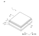
- FIG. 1 is a perspective view of the light emitting device according to the embodiment
- FIG. 2 is an exploded perspective view of the light emitting device shown in FIG. 1
- FIG. 3 (a) is a light emitting device taken along the line AA shown in FIG. 3 (b) is a perspective view of the microlens shown in FIG. 3 (a).
- the cross-sectional view shown in FIG. 3A is for explaining the structure of the light emitting device, and the scale of each component of the light emitting device is different from the scale of the actual component of the light emitting device. ..
- the light emitting device 1 has a cavity structure substrate 2, a VCSEL 3, a photodiode 4, and a microlens array 5.
- the cavity structure substrate 2 is formed of a mounting substrate 21 and a frame member 22, and has a recess 20 on which the VCSEL 3 and the photodiode 4 are mounted.
- the mounting substrate 21 is, for example, an aluminum nitride substrate, and a wiring pattern for supplying electric power to the VCSEL 3 and the photodiode 4 is arranged on the front surface, and an anode 23 and a cathode 24 for supplying electric power to the VCSEL 3 are arranged on the back surface.
- the frame member 22 is a frame-shaped member formed of a highly reflective member such as alumina and having through holes formed therein, and forms a recess 20 together with the mounting substrate 21.
- the VCSEL3 is also called a vertical cavity surface emitting laser (Vertical Cavity Surface Emitting Laser), and a plurality of emitters that emit laser light are arranged on the surface in an array at equal intervals.
- the VCSEL3 has, for example, 364 (26 ⁇ 14) emitters, and the 364 emitters are hexagonally arranged at a pitch of 0.0385 mm.
- the VCSEL 3 emits coherent laser light from the emitter toward the microlens array 5 according to the voltage applied between the anode 23 and the cathode 24.
- the divergence angle of the laser light emitted from the emitter is about 15 ° to 30 °, for example, 27 °.
- the VCSEL 3 is mounted on the cavity structure substrate 2 via the DB paste 6 containing the fine particle metal powder, and is electrically connected to the cathode 24. Further, the VCSEL 3 is electrically connected to the anode 23 via the bonding wire 7.
- the photodiode 4 receives the laser beam emitted by the VCSEL 3 and outputs a current corresponding to the received laser beam to a control device (not shown) arranged outside the light emitting device 1 via the photodiode electrode. ..
- the control device to which the current is input from the photodiode 4 controls the electric power supplied to the VCSEL 3 so as to make the light intensity of the laser light emitted from the VCSEL 3 a desired intensity.
- the microlens array 5 is a beam forming element such as a diffuser that beam forms the laser beam emitted by the VCSEL3.
- the microlens array 5 is fixed to the cavity structure substrate 2 by adhering the outer edge to the upper surface of the frame member 22 by the UV epoxy high-tixo-shaped adhesive 8.
- the area of the microlens array 5 when viewed in a plan view is smaller than the area of the outer edge of the frame member 22.
- the microlens array 5 can be adhered to the upper surface of the frame material 22 without the adhesive 8 flowing between the microlenses 51.
- the microlens array 5 By adhering the microlens array 5 to the frame material 22 using the high-tixo-shaped adhesive 8, it is not necessary to form an adhesive plane for arranging the adhesive on the outer edge of the microlens array 5. Since the microlens array 5 does not have to form an adhesive plane on the outer edge, it is easy to manufacture and the manufacturing cost can be suppressed.
- the area when the microlens array 5 is viewed in a plan view is smaller than the area of the outer edge of the frame member 22, when the stretching direction of the side of the microlens array 5 and the stretching direction of the side of the frame member 22 are deviated and bonded.
- the microlens array 5 protrudes from the outer edge of the frame member 22.
- Adhesion accuracy may be low, resulting in low manufacturing costs.
- the microlens array 5 can be arranged so as to cover the entire recess 20 even when the microlens array 5 is arranged at the time of bonding, and the lens position. The occurrence of optical loss due to misalignment or the like is suppressed.
- the microlens array 5 has a base material 50 and a plurality of microlenses 51 arranged so as to be aligned in the first direction and the second direction on the base material 50.
- the base material 50 has, for example, a rectangular planar shape formed of glass and formed by a pair of sides extending in the first direction and a pair of sides extending in the second direction orthogonal to the first direction.
- Each of the plurality of microlenses 51 is a convex lens formed of, for example, a thermoplastic resin such as a polyarylate resin, a thermosetting resin such as a silicone resin, and an ultraviolet curable resin such as an epoxy resin.
- the base material 50 and the plurality of microlenses 51 are formed as separate members, but in the microlens array according to the embodiment, the base material and the microlens may be integrally molded. ..
- the base material and the microlens may be integrally molded by injection molding a thermoplastic resin, a thermosetting resin, an ultraviolet curable resin, or the like.
- the microlens 51 may be formed as an aggregate of smaller lenses.
- each of the plurality of microlenses 51 is a plane surrounded by the ends of the curved surfaces 51b at which the curved surfaces 51b of the plurality of microlenses 51 start to stand, and each has a rectangular planar shape.
- each vertex T has a bottom surface 51a in the offset direction of any one of the first direction, the second direction, the third direction opposite to the first direction, and the fourth direction opposite to the second direction. Offset from the center point C of.
- the apex T of the microlens 51 is the portion farthest from the bottom surface 51a of the curved surface 51b of the microlens 51, and the center point C of the bottom surface 51a of the microlens 51 is the intersection of the diagonal lines of the bottom surface 51a.
- Each is divided into a microlens group 510 including a total of 16 microlenses in 4 rows ⁇ 4 columns having the same offset direction.
- reference patterns having different offset directions of the microlenses 51 included in the adjacent microlens group 510 are formed so as to repeatedly appear in the first direction and the second direction.
- the first pitch P1 which is the arrangement pitch of each of the plurality of microlenses 51 arranged in the first direction, is, for example, 0.075 mm, and is the second arrangement pitch of the plurality of microlenses 51 arranged in the second direction.
- the pitch P2 is, for example, 0.050 mm.
- FIG. 4A is a diagram showing a reference pattern 52 including 16 microlens groups 510.
- FIG. 4B is a plan view of the first microlens included in the reference pattern 52
- FIG. 4C is a plan view of the second microlens included in the reference pattern 52
- FIG. 4D is a plan view of the second microlens included in the reference pattern 52.
- FIG. 4 (e) is a plan view of the third microlens included in the reference pattern 52
- FIG. 4 (e) is a plan view of the fourth microlens included in the reference pattern 52.
- the reference pattern 52 has a first microlens group 511, a second microlens group 512, a third microlens group 513, and a fourth microlens group 514.
- Each of the first microlens group 511, the second microlens group 512, the third microlens group 513, and the fourth microlens group 514 includes a microlens group 510 containing a total of 16 microlenses 51 in 4 rows ⁇ 4 columns. Is.
- the apex T of the first microlens 511a included in the first microlens group 511 is offset in the first direction from the center point C of the bottom surface 51a, and the second microlens 512a included in the second microlens group 512 is of the bottom surface 51a.
- the vertex T is offset from the center point C in the second direction.
- the apex T of the third microlens 513a included in the third microlens group 513 is offset in the third direction from the center point C of the bottom surface 51a
- the fourth microlens 514a included in the fourth microlens group 514 is the bottom surface.
- the vertex T is offset from the center point C of 51a in the fourth direction.
- the microlens group 510 is a general term for the first microlens group 511, the second microlens group 512, the third microlens group 513, and the fourth microlens group 514.
- the microlens 51 is a general term for the first microlens 511a, the second microlens 512a, the third microlens 513a, and the fourth microlens 514a.
- the separation distance between the center point C and the apex T of the bottom surface 51a is the first offset distance O1
- the separation distance between the center point C and the apex T of the bottom surface 51a is the second offset distance O2
- the separation distance between the center point C and the apex T of the bottom surface 51a is the third offset distance O3
- the fourth microlens 514a the center point C and the apex T of the bottom surface 51a
- the separation distance between them is the fourth offset distance O4.
- the first offset distance O1 is the same as the third offset distance O3, and the second offset distance O2 is the same as the fourth offset distance O4.
- the first offset ratio R1 is indicated by the ratio of the first offset distance O1 to the first pitch P1, and in the second microlens group 512, the second offset ratio R2 is the second with respect to the second pitch P2. It is indicated by the ratio of 2 offset distances O2.
- the third offset ratio R3 is indicated by the ratio of the third offset distance O3 to the first pitch P1
- the fourth offset ratio R4 is the second with respect to the second pitch P2. It is indicated by the ratio of 4 offset distances O4.
- the first offset ratio R1 is the same as the second offset ratio R2, the third offset ratio R3, and the fourth offset ratio R4.
- the reference pattern 52 includes a total of 16 microlens groups 510 in four rows each in the first direction and the second direction.
- the fourth microlens group 514 is arranged adjacent to the first direction and the fourth direction of the first microlens group 511, and the second micron is arranged in the second direction and the third direction of the first microlens group 511.
- Lens groups 512 are arranged adjacent to each other.
- the offset directions of the microlenses 51 included in the second microlens group 512 and the fourth microlens group 514 adjacent to the first direction, the second direction, the third direction, and the fourth direction of the first microlens group 511 are the first. 1 It is orthogonal to the offset direction of the microlens 51 included in the microlens group 511.
- the first microlens group 511 is arranged adjacent to the first direction and the fourth direction of the second microlens group 512, and the third micro is arranged in the second direction and the third direction of the second microlens group 512.
- Lens groups 513 are arranged adjacent to each other.
- the offset directions of the microlenses 51 included in the first microlens group 511 and the third microlens group 513 adjacent to the first direction, the second direction, the third direction, and the fourth direction of the second microlens group 512 are the first. 2 It is orthogonal to the offset direction of the microlens 51 included in the microlens group 512.
- the second microlens group 512 is arranged adjacent to the first direction and the fourth direction of the third microlens group 513, and the fourth micro is arranged in the second direction and the third direction of the third microlens group 513.
- Lens groups 514 are arranged adjacent to each other.
- the offset directions of the microlenses 51 included in the second microlens group 512 and the fourth microlens group 514 adjacent to the first direction, the second direction, the third direction, and the fourth direction of the third microlens group 513 are the first. 3 It is orthogonal to the offset direction of the microlens 51 included in the microlens group 513.
- the third microlens group 513 is arranged adjacent to the first direction and the fourth direction of the fourth microlens group 514, and the first micron is arranged in the second direction and the third direction of the fourth microlens group 514.
- Lens groups 511 are arranged adjacent to each other.
- the offset directions of the microlenses 51 included in the first microlens group 511 and the third microlens group 513 adjacent to the first direction, the second direction, the third direction, and the fourth direction of the fourth microlens group 514 are the first. 4 It is orthogonal to the offset direction of the microlens 51 included in the microlens group 514.
- each of the first microlens group 511, the second microlens group 512, the third microlens group 513, and the fourth microlens group 514 is arranged in a row in the first direction.
- each of the first microlens group 511 to the fourth microlens group 514 is arranged in the first direction one by one in a row, it is per row of the first offset distance arranged in the first direction.
- the total value and the total value per row of the third offset distance are the same.
- the total value per row of the second offset distances arranged in the first direction and the total value per row of the fourth offset distances are the same.
- each of the first microlens group 511, the second microlens group 512, the third microlens group 513, and the fourth microlens group 514 is arranged in a row in the second direction.
- the total value of the distances per row of the first offset distances arranged in the second direction and the total value of the total values of the third offset distances per row are the same, and the second direction The total value per row of the second offset distances arranged in a row and the total value per row of the fourth offset distances are the same.
- FIG. 5A and 5B are views for explaining a preferable positional relationship between VCSEL3 and the microlens array 5
- FIG. 5A is a partial cross-sectional view of the light emitting device 1
- FIG. 5B is a microscopic view. It is a partial plan view of the lens array 5.
- the beam diameter ⁇ when the laser beam emitted from one point of the light source VCSEL3 reaches the apex is the vertical separation distance h between the surface of the VCSEL3 and the apex of the microlens 51, and the laser emitted by the VCSEL3. From the light divergence angle ⁇
- the first pitch PG1 which is the pitch in the first direction of the microlens group 510 with the beam diameter ⁇
- the second pitch PG2 which is the pitch in the second direction of the microlens group are 1.7 x PG1 ⁇ ⁇ ⁇ 16 x PG1 1.7 x PG2 ⁇ ⁇ ⁇ 16 x PG2 It is preferable to have a relationship with.
- FIG. 6 is a diagram showing the distribution of the beam light of VCSEL3 at the apex of the microlens 51 in the light emitting device 1.
- the broken line indicates the inner wall of the frame member 22.
- the separation distance between the VCSEL 3 and the apex of the microlens 51 is 0.4 mm.
- the beam diameter of the laser beam 515 emitted from the VCSEL 3 at the apex of the microlens 51 is 0.192 mm.
- the first pitch PG1 and the second pitch PG2 which are the pitches of the microlens group 510 in the first and second directions.
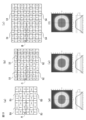
- FIG. 7 is a diagram showing an illuminance distribution calculated by simulation when the ratio of the first pitch PG1 and the second pitch PG2 is 4: 3.
- FIG. 7A shows an illuminance distribution when the beam diameter ⁇ is 1.04 times that of the first pitch PG1 and 1.39 times that of the second pitch PG2.
- FIG. 7B shows the illuminance distribution when the beam diameter ⁇ is 1.22 times that of the first pitch PG1 and 1.63 times that of the second pitch PG2.
- FIG. 7C shows the illuminance distribution when the beam diameter ⁇ is 1.40 times that of the first pitch PG1 and 1.89 times that of the second pitch PG2.
- FIG. 7A shows an illuminance distribution when the beam diameter ⁇ is 1.04 times that of the first pitch PG1 and 1.39 times that of the second pitch PG2.
- FIG. 7B shows the illuminance distribution when the beam diameter ⁇ is 1.22 times that of the first pitch PG1 and 1.63 times that of the second pitch PG2.
- FIGS. 7 (a) to 7 (f) shows the illuminance distribution when the beam diameter ⁇ is 1.92 times that of the first pitch PG1 and 2.56 times that of the second pitch PG2.
- the upper figure is a two-dimensional image showing the illuminance distribution of the laser beam emitted from the light emitting device 1
- the lower figure is a diagram showing the illuminance distribution in the first direction.
- FIG. 8 is a diagram showing an illuminance distribution calculated by simulation when the ratio of the first pitch PG1 and the second pitch PG2 is 1: 1.
- FIG. 8A shows the illuminance distribution when the beam diameter ⁇ is 1.04 times that of the first pitch PG1 and the second pitch PG2.
- FIG. 8B shows the illuminance distribution when the beam diameter ⁇ is 1.22 times that of the first pitch PG1 and the second pitch PG2.
- FIG. 8C shows the illuminance distribution when the beam diameter ⁇ is 1.40 times that of the first pitch PG1 and the second pitch PG2.
- FIG. 8D shows the illuminance distribution when the beam diameter ⁇ is 1.58 times that of the first pitch PG1 and the second pitch PG2.
- FIG. 8A shows the illuminance distribution when the beam diameter ⁇ is 1.04 times that of the first pitch PG1 and the second pitch PG2.
- FIG. 8B shows the illuminance distribution when the beam diameter ⁇ is 1.22 times that of the
- FIG. 8E shows the illuminance distribution when the beam diameter ⁇ is 1.74 times that of the first pitch PG1 and the second pitch PG2.
- FIG. 8 (f) shows the illuminance distribution when the beam diameter ⁇ is 1.92 times that of the first pitch PG1 and the second pitch PG2.
- the upper figure is a two-dimensional image showing the illuminance distribution of the laser beam emitted from the light emitting device 1
- the lower figure is a diagram showing the illuminance distribution in the first direction.
- the divergence angle of the laser beam emitted from VCSEL3 is about 15 ° to 30 °, and the minimum values of the first pitch PG1 and the second pitch PG2 that can be manufactured are about 20 ⁇ m.
- the separation distance h between the VCSEL 3 and the apex of the microlens 51 is about 0.2 mm to 0.6 mm.
- the minimum value of the separation distance h between the VCSEL 3 and the apex of the microlens 51, 0.2 mm, is a distance at which the microlens 51 does not come into contact with the bonding wire 7.
- the maximum value of the separation distance h between the VCSEL 3 and the apex of the microlens 51, 0.6 mm, is a distance determined from the viewpoint of miniaturization.
- the preferable value of the separation distance h between the VCSEL 3 and the apex of the microlens 51 is 0.4 mm.
- the beam diameter ⁇ is set to 0.6 mm, which is the maximum value of the separation distance h between the VCSEL 3 and the apex of the microlens 51, and 30 °, which is the maximum value of the divergence angle of the laser beam emitted from the VCSEL 3 (1). It is calculated by substituting into. 16 which is the maximum multiple of the first pitch PG1 and the second pitch PG2 of the beam diameter ⁇ is the beam diameter ⁇ calculated by the equation (1) at 20 ⁇ m which is the minimum value of the first pitch PG1 and the second pitch PG2. It is calculated by dividing.
- FIG. 9 is a diagram showing a change in the illuminance distribution when the offset rate of the apex from the center point of the bottom surface of the microlens 51 is changed.
- FIG. 9A shows a case where the first offset rate R1 and the second offset rate R2 are zero
- FIG. 9B shows a case where the first offset rate R1 and the second offset rate R2 are the first pitch P1 and the second pitch. The case where it is 5% of P2 is shown.
- FIG. 9C shows a case where the first offset rate R1 and the second offset rate R2 are 10% of the first pitch P1 and the second pitch P2
- FIG. 9D shows the case where the first offset rate R1 and the second offset rate R2 are used.
- FIG. 9 (e) shows a case where the first offset rate R1 and the second offset rate R2 are 20% of the first pitch P1 and the second pitch P2, and FIG. 9 (f) shows the first offset rate R1 and the second.
- the case where the offset rate R2 is 25% of the first pitch P1 and the second pitch P2 is shown.
- 9 (a) to 9 (f) the above figure is a two-dimensional image showing the illuminance distribution of the image displayed on the screen which is the irradiation region where the laser beam emitted from the light emitting device 1 is irradiated.
- the figure below is a diagram showing the illuminance distribution in the first direction.
- the separation distance between the light emitting device 1 and the screen on which the image is displayed is 50 cm, and the screen on which the image is displayed has a square shape with a side length of 100 cm.
- the illuminance distribution of the image displayed on the screen changes from a substantially rectangular shape to a substantially elliptical shape. It transforms into.
- Table 1 shows the average irradiance of the region where the divergence angle is within the range of 60 ° in the first direction and the divergence angle is within the range of 45 ° in the second direction.
- the irradiance ratio indicates the ratio of irradiance according to the change in the offset rate when the offset rate of the apex from the center point in the first direction and the second direction is zero as 100%. ..
- the irradiance ratio is 90% when the offset rate is 20% or less of the first pitch P1 and the second pitch P2, and maintains a substantially rectangular shape. However, the irradiance ratio is less than 90% when the offset rate is 25% of the first pitch P1 and the second pitch P2, and changes from a substantially rectangular shape to a substantially elliptical shape. Therefore, the offset rate is preferably 20% or less of the first pitch P1 and the second pitch P2.
- FIG. 10 is a diagram showing a change in the distribution of interference fringes when the offset rate of the apex from the center point of the bottom surface of the microlens 51 is changed.
- FIG. 10A shows a case where the first offset rate R1 and the second offset rate R2 are zero
- FIG. 10B shows a case where the first offset rate R1 and the second offset rate R2 are the first pitch P1 and the second pitch. The case where it is 5% of P2 is shown.
- FIG. 10 (c) shows a case where the first offset rate R1 and the second offset rate R2 are 10% of the first pitch P1 and the second pitch P2
- FIG. 10 (d) shows the first offset rate R1 and the second.
- FIG. 10 (e) shows a case where the first offset rate R1 and the second offset rate R2 are 20% of the first pitch P1 and the second pitch P2, and FIG. 10 (f) shows the first offset rate R1 and the second.
- the case where the offset rate R2 is 25% of the first pitch P1 and the second pitch P2 is shown.
- the upper figure is a two-dimensional image showing the distribution of interference fringes of the image displayed on the screen by the laser beam emitted from the light emitting device 1, and the lower figure is the first direction. It is a figure which shows the intensity distribution of the interference fringe.
- the image displayed on the screen has interference fringes distributed with strong intensity over the entire surface.
- the offset rate is 5% or more of the first pitch P1 and the second pitch P2
- the intensity of the interference fringes is significantly reduced as compared with the case where the offset rate of the vertices is zero.
- the interference fringes gradually decrease as the offset ratio of the vertices increases.
- the offset rate of the microlens 51 when the offset rate of the microlens 51 is 5% or more, the interference fringes are significantly reduced, and when the offset rate of the microlens 51 is 20% or less, the irradiance ratio is 90% or more. .. Therefore, the offset rate of the microlens 51 is preferably 5% or more and 20% or less. Further, when the offset rate of the microlens 51 is 5% or more, the interference fringes are further reduced. Therefore, the offset rate of the microlens 51 is more preferably 15% or more and 20% or less.
- the microlens array 5 improves the uniformity of the intensity of the light applied to the irradiation region by arranging the microlenses 51 whose vertices are offset from the center point so that the reference patterns 52 appear repeatedly while being adjacent to each other. Can be done.
- the design depends on an uncertain element called random, and the result unintended by the designer is obtained. Since it may be obtained, it is necessary to repeat the optical simulation in order to obtain the result intended by the designer, which may increase the design load. That is, it is not easy to strictly control the arrangement of the vertices of the lens, and it is not easy to control the directivity of the lens in which the vertices are arranged at random.
- the microlens array 5 By arranging the microlens array 5 so that the reference patterns 52 appear repeatedly while being adjacent to each other, the directivity can be controlled with high accuracy and easily.
- the design cost may increase because the optical simulation is repeatedly executed to optimize the optical characteristics.
- the optical characteristics can be optimized by designing the reference pattern 52, so that the design cost can be suppressed as compared with the lens in which the vertices are randomly arranged.
- the microlens group 510 is arranged so that the directions in which the apex T is offset from the microlens group 510 adjacent to the first direction, the second direction, the third direction, and the fourth direction are orthogonal to each other. As a result, the uniformity of the intensity of the light applied to the irradiation region can be further improved.
- the first offset distance O1 between the center point C and the apex T in the first microlens group 511 is the first between the center point C and the apex T in the third microlens group 513. It is the same as the 3 offset O3 distance.
- the second offset distance O2 between the center point C and the apex T in the second microlens group 512 is the same as the fourth offset distance O4 between the center point C and the apex T in the fourth microlens group 514. Is.
- the first offset distance O1 and the third offset distance O3, which are offset in opposite directions, and the second offset distance O2 and the fourth offset distance O4 are made the same to enhance the regularity of the offset, thereby increasing the regularity of the offset.
- the uniformity of the intensity of the light irradiated to the can be further improved.
- first offset ratio R1 and the third offset ratio R3 in the first microlens group 511 and the third microlens group 513 are the second offset ratio R2 and the third offset ratio R2 in the second microlens group 512 and the fourth microlens group 514.
- the offset ratio is the same as R4.
- the microlens array 5 sets the first offset ratio R1 and the third offset ratio R3 and the second offset ratio R2 and the fourth offset ratio R4 to be the same to enhance the regularity of the offset, thereby increasing the intensity of the light applied to the irradiation region. Uniformity can be further improved.
- the microlens array 5 is a laser capable of suppressing interference fringes and irradiating an irradiation region with a uniform intensity by setting the first offset ratio R1 and the second offset ratio R2 to 5% or more and 20% or less. It can emit light.
- the total value per row of the first offset distance O1 is the same as the total value per row of the third offset distance O3, and the first The total value per row of the two offset distances O2 becomes the same as the total value per row of the fourth offset distance O4.
- the microlens array 5 sets the total value per row of the first offset distance O1 and the third offset distance O3 arranged in the first direction, and the total value per row of the second offset distance O2 and the fourth offset distance O4. By making them the same, the uniformity of the intensity of the light applied to the irradiation region can be further improved.
- the total value per row of the first offset distance O1 is the same as the total value per row of the third offset distance O3, and the third offset distance O3 is the same.
- the total value per row of the two offset distances O2 becomes the same as the total value per row of the fourth offset distance O4.
- the microlens array 5 sets the total value per row of the first offset distance O1 and the third offset distance O3 arranged in the second direction, and the total value per row of the second offset distance O2 and the fourth offset distance O4. By making them the same, the uniformity of the intensity of the light applied to the irradiation region can be further improved.
- the beam diameter when the laser beam reaches the microlens 51 is 1.7 times or more and 16 times or less the arrangement pitch in the first direction and the second direction of the microlens group 510. Therefore, the interference fringes are not unevenly distributed, and the irradiation region can be irradiated with a uniform intensity.
- FIGS. 1 to 10 (Modified example of the microlens array according to the embodiment) Although the light emitting device 1 and the microlens array 5 which are examples of the light emitting device and the microlens array according to the embodiment have been described with reference to FIGS. 1 to 10, the microlens array according to the embodiment is shown in FIGS. 1 to 10. It is not limited to the embodiments described with reference to it.
- the first offset distance O1 of the first microlens group 511 may be different from the third offset distance O3 of the third microlens group 513
- the second offset distance O2 of the second microlens group 512 may be the fourth micro. It may be different from the fourth offset distance 4 of the lens group 514.
- the plurality of microlenses 51 are convex lenses, in the microlens array according to the embodiment, the plurality of microlenses may be concave lenses.
- the reference pattern 52 includes a total of 16 microlens groups 510 in 4 rows and 4 columns, but in the microlens array according to the embodiment, the number of microlens groups included in the reference pattern is It is not limited to a total of 16 lenses in 4 rows and 4 columns.
- FIG. 11 is a diagram showing a reference pattern according to the first modification.
- the reference pattern 53 includes a total of nine microlens groups 510 in three rows each in the first direction and the second direction.
- the reference pattern 53 includes two first microlens groups 511, three second microlens groups 512, two third microlens groups 513, and two fourth microlens groups 514.
- each of the first microlens group 511 to the fourth microlens group 514 has a direction in which the apex is offset from the microlens group adjacent to the first direction, the second direction, the third direction, and the fourth direction. Arranged so as to be orthogonal.
- FIG. 12 is a diagram showing a reference pattern according to the second modification.
- the reference pattern 54 includes a total of 25 microlens groups 510 in 5 rows each in the first direction and the second direction.
- the reference pattern 54 includes six first microlens groups 511, seven second microlens groups 512, six third microlens groups 513, and six fourth microlens groups 514.
- each of the first microlens group 511 to the fourth microlens group 514 has a direction in which the apex is offset from the microlens group adjacent to the first direction, the second direction, the third direction, and the fourth direction. Arranged so as to be orthogonal.
- the same number of microlens groups 510 are arranged in the first direction and the second direction, but in the microlens array according to the embodiment, the microlens groups 510 arranged in the first direction.
- the number of may be different from the number of the microlens group 510 arranged in the second direction.
- FIG. 13 is a diagram showing the comparison results of the illuminance distributions of the reference pattern 52 according to the embodiment, the reference pattern 53 according to the first modification, and the reference pattern 54 according to the second modification.
- FIG. 13 (a) shows the arrangement of the reference pattern 53 including the microlens group 510 of 3 rows and 3 columns
- FIG. 13 (b) shows the arrangement of the reference pattern 52 including the micro lens group 510 of 4 rows and 4 columns.
- FIG. 13 (c) shows an array of reference patterns 54 including a 5 row 5 column microlens group 510.
- 13 (d) shows the illuminance distribution of the reference pattern 53
- FIG. 13 (e) shows the illuminance distribution of the reference pattern 52
- FIG. 13 (f) shows the illuminance distribution of the reference pattern 54.
- the microlens group 510 of the adjacent reference pattern 53 and the microlens group 510 having one side in contact with each other are arranged so that the offset directions are opposite to each other. And are not orthogonal to each other.
- the offset directions of the microlens group 510 of the adjacent reference pattern 53 and the microlens group 510 whose one side is in contact with each other are not orthogonal to each other, interference fringes are more likely to occur than the reference pattern 52.
- the offset directions of the microlens group 510 of the adjacent reference pattern 54 and the microlens group 510 having one side in contact with each other are oriented in the same direction or opposite to each other. They are arranged so that they face each other and are not orthogonal to each other. Since the reference pattern 54 includes a pattern in which the microlens group 510 of the adjacent reference pattern 54 and the microlens group 510 whose one side is in contact with each other are arranged so that the offset directions are in the same direction, interference fringes are further formed as compared with the reference pattern 53. It is easy to occur.
- the offset directions of the microlens group 510 included in the adjacent reference pattern 53 are all arranged so as to be orthogonal to each other, so that the reference pattern 53 and the reference pattern 53 and the reference pattern 53 are arranged so as to be orthogonal to each other. Interference fringes are less likely to occur than 54.
- the illuminance distribution of the reference pattern 52 including the even-numbered microlens group 510 has less distortion than the illuminance distribution of the reference pattern 53 and the reference pattern 54 including the odd-numbered microlens group 510, and the reference pattern is smaller than the odd-numbered row. It is preferable to include an even-numbered row of microlens groups 510.
- the number of microlens groups arranged in each of the first direction and the second direction is preferably an even number of 4 or more.
- the number of microlens groups arranged in each of the first direction and the second direction is more preferably 4 or 8.
- the reference pattern in which the number of microlens groups arranged in each of the first direction and the second direction is eight is formed by arranging four reference patterns 52.
- reference patterns in which the vertices of adjacent microlens groups 510 are offset in a predetermined direction are formed so as to repeatedly appear in the first direction and the second direction.
- reference patterns in which the vertices of adjacent microlenses 51 are offset in predetermined directions may be formed so as to repeatedly appear in the first direction and the second direction.
- FIG. 14A is a diagram showing a reference pattern according to the third modification
- FIG. 14B is a diagram showing an illuminance distribution calculated by simulating a microlens array having the reference pattern according to the third modification. Is.
- the reference pattern 55 according to the third modification includes a total of 16 microlenses 51 in four rows each in the first direction and the second direction.
- the reference pattern 55 includes two first microlens groups 511, three second microlens groups 512, two third microlens groups 513, and two fourth microlens groups 514.
- the reference pattern 55 similarly to the reference patterns 52 to 54, it is possible to irradiate the irradiation region with light having high intensity uniformity.
Landscapes
- Physics & Mathematics (AREA)
- Engineering & Computer Science (AREA)
- General Engineering & Computer Science (AREA)
- General Physics & Mathematics (AREA)
- Optics & Photonics (AREA)
- Condensed Matter Physics & Semiconductors (AREA)
- Electromagnetism (AREA)
- Semiconductor Lasers (AREA)
Priority Applications (1)
| Application Number | Priority Date | Filing Date | Title |
|---|---|---|---|
| JP2021567580A JP7369210B2 (ja) | 2019-12-24 | 2020-12-23 | マイクロレンズアレイ及び発光装置 |
Applications Claiming Priority (2)
| Application Number | Priority Date | Filing Date | Title |
|---|---|---|---|
| JP2019233380 | 2019-12-24 | ||
| JP2019-233380 | 2019-12-24 |
Publications (1)
| Publication Number | Publication Date |
|---|---|
| WO2021132401A1 true WO2021132401A1 (ja) | 2021-07-01 |
Family
ID=76574330
Family Applications (1)
| Application Number | Title | Priority Date | Filing Date |
|---|---|---|---|
| PCT/JP2020/048301 Ceased WO2021132401A1 (ja) | 2019-12-24 | 2020-12-23 | マイクロレンズアレイ及び発光装置 |
Country Status (2)
| Country | Link |
|---|---|
| JP (1) | JP7369210B2 (https=) |
| WO (1) | WO2021132401A1 (https=) |
Citations (4)
| Publication number | Priority date | Publication date | Assignee | Title |
|---|---|---|---|---|
| US20110284725A1 (en) * | 2008-03-04 | 2011-11-24 | The Regents Of The Univeristy Of California | Microlens arrays for enhanced light concentration |
| JP2016224212A (ja) * | 2015-05-29 | 2016-12-28 | ミツミ電機株式会社 | 光走査制御装置 |
| JP2018200489A (ja) * | 2018-08-31 | 2018-12-20 | 株式会社リコー | レンズアレイ、画像表示装置、及び移動体 |
| JP2019092145A (ja) * | 2017-11-16 | 2019-06-13 | 采▲ぎょく▼科技股▲ふん▼有限公司VisEra Technologies Company Limited | シフトされたマイクロレンズアレイを有するイメージセンサ |
Family Cites Families (3)
| Publication number | Priority date | Publication date | Assignee | Title |
|---|---|---|---|---|
| JP2007133095A (ja) * | 2005-11-09 | 2007-05-31 | Sharp Corp | 表示装置とその製造方法 |
| KR100731094B1 (ko) * | 2005-12-28 | 2007-06-22 | 동부일렉트로닉스 주식회사 | 씨모스 이미지 센서 및 그 제조방법 |
| JP2018201061A (ja) * | 2017-05-25 | 2018-12-20 | ソニーセミコンダクタソリューションズ株式会社 | 固体撮像装置 |
-
2020
- 2020-12-23 JP JP2021567580A patent/JP7369210B2/ja active Active
- 2020-12-23 WO PCT/JP2020/048301 patent/WO2021132401A1/ja not_active Ceased
Patent Citations (4)
| Publication number | Priority date | Publication date | Assignee | Title |
|---|---|---|---|---|
| US20110284725A1 (en) * | 2008-03-04 | 2011-11-24 | The Regents Of The Univeristy Of California | Microlens arrays for enhanced light concentration |
| JP2016224212A (ja) * | 2015-05-29 | 2016-12-28 | ミツミ電機株式会社 | 光走査制御装置 |
| JP2019092145A (ja) * | 2017-11-16 | 2019-06-13 | 采▲ぎょく▼科技股▲ふん▼有限公司VisEra Technologies Company Limited | シフトされたマイクロレンズアレイを有するイメージセンサ |
| JP2018200489A (ja) * | 2018-08-31 | 2018-12-20 | 株式会社リコー | レンズアレイ、画像表示装置、及び移動体 |
Also Published As
| Publication number | Publication date |
|---|---|
| JP7369210B2 (ja) | 2023-10-25 |
| JPWO2021132401A1 (https=) | 2021-07-01 |
Similar Documents
| Publication | Publication Date | Title |
|---|---|---|
| CN104583668B (zh) | Led背光源的照明透镜、发光设备、表面光源设备、显示设备 | |
| JP5963858B2 (ja) | 光電子モジュール、光電子装置及び方法 | |
| US10837619B2 (en) | Optical system for multi-emitter LED-based lighting devices | |
| US12169064B2 (en) | Microstructures for transforming light having Lambertian distribution into batwing distributions | |
| KR102673806B1 (ko) | 3차원 거리 측정 시스템에서의 사용을 위한 선 패턴 프로젝터 | |
| JP2011138982A (ja) | 照明装置および照明装置の製造方法 | |
| US10498109B1 (en) | Projector of Structured light pattern | |
| CN114895505B (zh) | 用于实现激光点阵的投射模组 | |
| CN111649261A (zh) | 电子装置 | |
| CN115668668A (zh) | 发光装置及测距装置 | |
| CN111065886A (zh) | 生成结构光 | |
| CN113777680A (zh) | 一种光学扩散片及光发射模组 | |
| CN220303493U (zh) | 照明装置和照明设备 | |
| CN104396101B (zh) | 均质线形强度轮廓的激光器模块 | |
| CN113281909A (zh) | 衍射光学元件、投射模组及电子设备 | |
| JP7369210B2 (ja) | マイクロレンズアレイ及び発光装置 | |
| CN106287407A (zh) | 改变光线指向的膜及背光模组 | |
| JP7277614B2 (ja) | Vcselベースのパターンプロジェクタ | |
| KR20230000915A (ko) | 3차원 거리 측정 시스템에 사용하기 위한 도트 패턴 프로젝터 | |
| JP2022019243A (ja) | マイクロレンズアレイ及びマイクロレンズアレイの製造方法 | |
| CN101490597B (zh) | 使光均匀化的装置和用于在工作面内产生线性光强分布的激光装置 | |
| KR102159203B1 (ko) | 광 형상화 및 균질화를 위한 마이크로렌즈 어레이 | |
| CN112824941A (zh) | 微透镜阵列元件以及扩散片和电子设备 | |
| CN217543555U (zh) | 点阵结构光系统 | |
| CN114079224A (zh) | 光学元件和晶圆级光学模块 |
Legal Events
| Date | Code | Title | Description |
|---|---|---|---|
| 121 | Ep: the epo has been informed by wipo that ep was designated in this application |
Ref document number: 20907779 Country of ref document: EP Kind code of ref document: A1 |
|
| DPE1 | Request for preliminary examination filed after expiration of 19th month from priority date (pct application filed from 20040101) | ||
| ENP | Entry into the national phase |
Ref document number: 2021567580 Country of ref document: JP Kind code of ref document: A |
|
| NENP | Non-entry into the national phase |
Ref country code: DE |
|
| 122 | Ep: pct application non-entry in european phase |
Ref document number: 20907779 Country of ref document: EP Kind code of ref document: A1 |