WO2021132143A1 - Antenne, module de communication sans fil et dispositif de communication sans fil - Google Patents
Antenne, module de communication sans fil et dispositif de communication sans fil Download PDFInfo
- Publication number
- WO2021132143A1 WO2021132143A1 PCT/JP2020/047650 JP2020047650W WO2021132143A1 WO 2021132143 A1 WO2021132143 A1 WO 2021132143A1 JP 2020047650 W JP2020047650 W JP 2020047650W WO 2021132143 A1 WO2021132143 A1 WO 2021132143A1
- Authority
- WO
- WIPO (PCT)
- Prior art keywords
- conductor
- antenna
- reinforcing member
- conductors
- plane
- Prior art date
Links
- 238000004891 communication Methods 0.000 title claims abstract description 41
- 239000004020 conductor Substances 0.000 claims abstract description 833
- 239000003989 dielectric material Substances 0.000 claims abstract description 20
- 230000003014 reinforcing effect Effects 0.000 claims description 234
- 230000005855 radiation Effects 0.000 claims description 22
- 230000007774 longterm Effects 0.000 abstract description 4
- 230000002787 reinforcement Effects 0.000 abstract 2
- 239000000758 substrate Substances 0.000 description 25
- 229910000679 solder Inorganic materials 0.000 description 20
- 239000000463 material Substances 0.000 description 11
- 238000010586 diagram Methods 0.000 description 6
- 239000011347 resin Substances 0.000 description 6
- 229920005989 resin Polymers 0.000 description 6
- 230000000694 effects Effects 0.000 description 5
- 239000007769 metal material Substances 0.000 description 5
- 230000006870 function Effects 0.000 description 4
- 239000011810 insulating material Substances 0.000 description 4
- 229920000642 polymer Polymers 0.000 description 4
- 230000008878 coupling Effects 0.000 description 3
- 238000010168 coupling process Methods 0.000 description 3
- 238000005859 coupling reaction Methods 0.000 description 3
- PXHVJJICTQNCMI-UHFFFAOYSA-N Nickel Chemical compound [Ni] PXHVJJICTQNCMI-UHFFFAOYSA-N 0.000 description 2
- KDLHZDBZIXYQEI-UHFFFAOYSA-N Palladium Chemical compound [Pd] KDLHZDBZIXYQEI-UHFFFAOYSA-N 0.000 description 2
- 239000004962 Polyamide-imide Substances 0.000 description 2
- 239000004697 Polyetherimide Substances 0.000 description 2
- RTAQQCXQSZGOHL-UHFFFAOYSA-N Titanium Chemical compound [Ti] RTAQQCXQSZGOHL-UHFFFAOYSA-N 0.000 description 2
- 229910045601 alloy Inorganic materials 0.000 description 2
- 239000000956 alloy Substances 0.000 description 2
- 229910052782 aluminium Inorganic materials 0.000 description 2
- XAGFODPZIPBFFR-UHFFFAOYSA-N aluminium Chemical compound [Al] XAGFODPZIPBFFR-UHFFFAOYSA-N 0.000 description 2
- 239000011230 binding agent Substances 0.000 description 2
- 230000005540 biological transmission Effects 0.000 description 2
- 229910010293 ceramic material Inorganic materials 0.000 description 2
- 229920001940 conductive polymer Polymers 0.000 description 2
- 239000003822 epoxy resin Substances 0.000 description 2
- 239000011521 glass Substances 0.000 description 2
- 238000005259 measurement Methods 0.000 description 2
- 229910052751 metal Inorganic materials 0.000 description 2
- 239000002184 metal Substances 0.000 description 2
- 239000000203 mixture Substances 0.000 description 2
- BASFCYQUMIYNBI-UHFFFAOYSA-N platinum Chemical compound [Pt] BASFCYQUMIYNBI-UHFFFAOYSA-N 0.000 description 2
- 230000010287 polarization Effects 0.000 description 2
- 229920002312 polyamide-imide Polymers 0.000 description 2
- 229920000647 polyepoxide Polymers 0.000 description 2
- 229920001225 polyester resin Polymers 0.000 description 2
- 239000004645 polyester resin Substances 0.000 description 2
- 229920001601 polyetherimide Polymers 0.000 description 2
- 229920001721 polyimide Polymers 0.000 description 2
- 239000009719 polyimide resin Substances 0.000 description 2
- 239000010936 titanium Substances 0.000 description 2
- 229910052719 titanium Inorganic materials 0.000 description 2
- VYZAMTAEIAYCRO-UHFFFAOYSA-N Chromium Chemical compound [Cr] VYZAMTAEIAYCRO-UHFFFAOYSA-N 0.000 description 1
- RYGMFSIKBFXOCR-UHFFFAOYSA-N Copper Chemical compound [Cu] RYGMFSIKBFXOCR-UHFFFAOYSA-N 0.000 description 1
- 229920000106 Liquid crystal polymer Polymers 0.000 description 1
- 239000004977 Liquid-crystal polymers (LCPs) Substances 0.000 description 1
- WHXSMMKQMYFTQS-UHFFFAOYSA-N Lithium Chemical compound [Li] WHXSMMKQMYFTQS-UHFFFAOYSA-N 0.000 description 1
- BUGBHKTXTAQXES-UHFFFAOYSA-N Selenium Chemical compound [Se] BUGBHKTXTAQXES-UHFFFAOYSA-N 0.000 description 1
- BQCADISMDOOEFD-UHFFFAOYSA-N Silver Chemical compound [Ag] BQCADISMDOOEFD-UHFFFAOYSA-N 0.000 description 1
- ATJFFYVFTNAWJD-UHFFFAOYSA-N Tin Chemical compound [Sn] ATJFFYVFTNAWJD-UHFFFAOYSA-N 0.000 description 1
- 230000001133 acceleration Effects 0.000 description 1
- 239000002253 acid Substances 0.000 description 1
- HSFWRNGVRCDJHI-UHFFFAOYSA-N alpha-acetylene Natural products C#C HSFWRNGVRCDJHI-UHFFFAOYSA-N 0.000 description 1
- 239000012298 atmosphere Substances 0.000 description 1
- ZIXVIWRPMFITIT-UHFFFAOYSA-N cadmium lead Chemical compound [Cd].[Pb] ZIXVIWRPMFITIT-UHFFFAOYSA-N 0.000 description 1
- 230000008859 change Effects 0.000 description 1
- 239000003795 chemical substances by application Substances 0.000 description 1
- 229910052804 chromium Inorganic materials 0.000 description 1
- 239000011651 chromium Substances 0.000 description 1
- 229910017052 cobalt Inorganic materials 0.000 description 1
- 239000010941 cobalt Substances 0.000 description 1
- GUTLYIVDDKVIGB-UHFFFAOYSA-N cobalt atom Chemical compound [Co] GUTLYIVDDKVIGB-UHFFFAOYSA-N 0.000 description 1
- 229910052802 copper Inorganic materials 0.000 description 1
- 239000010949 copper Substances 0.000 description 1
- PMHQVHHXPFUNSP-UHFFFAOYSA-M copper(1+);methylsulfanylmethane;bromide Chemical compound Br[Cu].CSC PMHQVHHXPFUNSP-UHFFFAOYSA-M 0.000 description 1
- 239000013078 crystal Substances 0.000 description 1
- 238000006073 displacement reaction Methods 0.000 description 1
- 238000005516 engineering process Methods 0.000 description 1
- 239000002241 glass-ceramic Substances 0.000 description 1
- PCHJSUWPFVWCPO-UHFFFAOYSA-N gold Chemical compound [Au] PCHJSUWPFVWCPO-UHFFFAOYSA-N 0.000 description 1
- 229910052737 gold Inorganic materials 0.000 description 1
- 239000010931 gold Substances 0.000 description 1
- 238000009413 insulation Methods 0.000 description 1
- 229910052744 lithium Inorganic materials 0.000 description 1
- WPBNNNQJVZRUHP-UHFFFAOYSA-L manganese(2+);methyl n-[[2-(methoxycarbonylcarbamothioylamino)phenyl]carbamothioyl]carbamate;n-[2-(sulfidocarbothioylamino)ethyl]carbamodithioate Chemical compound [Mn+2].[S-]C(=S)NCCNC([S-])=S.COC(=O)NC(=S)NC1=CC=CC=C1NC(=S)NC(=O)OC WPBNNNQJVZRUHP-UHFFFAOYSA-L 0.000 description 1
- 238000000034 method Methods 0.000 description 1
- 239000010445 mica Substances 0.000 description 1
- 229910052618 mica group Inorganic materials 0.000 description 1
- 229910052759 nickel Inorganic materials 0.000 description 1
- 230000003287 optical effect Effects 0.000 description 1
- 239000003960 organic solvent Substances 0.000 description 1
- TWNQGVIAIRXVLR-UHFFFAOYSA-N oxo(oxoalumanyloxy)alumane Chemical compound O=[Al]O[Al]=O TWNQGVIAIRXVLR-UHFFFAOYSA-N 0.000 description 1
- 229910052763 palladium Inorganic materials 0.000 description 1
- 229910052697 platinum Inorganic materials 0.000 description 1
- 229920001197 polyacetylene Polymers 0.000 description 1
- 229920000767 polyaniline Polymers 0.000 description 1
- 229920000128 polypyrrole Polymers 0.000 description 1
- 229920000123 polythiophene Polymers 0.000 description 1
- 239000000843 powder Substances 0.000 description 1
- 230000008569 process Effects 0.000 description 1
- 229910052711 selenium Inorganic materials 0.000 description 1
- 239000011669 selenium Substances 0.000 description 1
- 239000004065 semiconductor Substances 0.000 description 1
- 229910052709 silver Inorganic materials 0.000 description 1
- 239000004332 silver Substances 0.000 description 1
- 239000000779 smoke Substances 0.000 description 1
- 230000007480 spreading Effects 0.000 description 1
- 229910052718 tin Inorganic materials 0.000 description 1
- 239000011135 tin Substances 0.000 description 1
- 229910052720 vanadium Inorganic materials 0.000 description 1
- LEONUFNNVUYDNQ-UHFFFAOYSA-N vanadium atom Chemical compound [V] LEONUFNNVUYDNQ-UHFFFAOYSA-N 0.000 description 1
Images


Classifications
-
- H—ELECTRICITY
- H01—ELECTRIC ELEMENTS
- H01Q—ANTENNAS, i.e. RADIO AERIALS
- H01Q9/00—Electrically-short antennas having dimensions not more than twice the operating wavelength and consisting of conductive active radiating elements
- H01Q9/04—Resonant antennas
- H01Q9/0407—Substantially flat resonant element parallel to ground plane, e.g. patch antenna
- H01Q9/045—Substantially flat resonant element parallel to ground plane, e.g. patch antenna with particular feeding means
- H01Q9/0457—Substantially flat resonant element parallel to ground plane, e.g. patch antenna with particular feeding means electromagnetically coupled to the feed line
-
- H—ELECTRICITY
- H01—ELECTRIC ELEMENTS
- H01Q—ANTENNAS, i.e. RADIO AERIALS
- H01Q1/00—Details of, or arrangements associated with, antennas
- H01Q1/12—Supports; Mounting means
- H01Q1/22—Supports; Mounting means by structural association with other equipment or articles
- H01Q1/24—Supports; Mounting means by structural association with other equipment or articles with receiving set
-
- H—ELECTRICITY
- H01—ELECTRIC ELEMENTS
- H01Q—ANTENNAS, i.e. RADIO AERIALS
- H01Q1/00—Details of, or arrangements associated with, antennas
- H01Q1/36—Structural form of radiating elements, e.g. cone, spiral, umbrella; Particular materials used therewith
- H01Q1/38—Structural form of radiating elements, e.g. cone, spiral, umbrella; Particular materials used therewith formed by a conductive layer on an insulating support
-
- H—ELECTRICITY
- H01—ELECTRIC ELEMENTS
- H01Q—ANTENNAS, i.e. RADIO AERIALS
- H01Q5/00—Arrangements for simultaneous operation of antennas on two or more different wavebands, e.g. dual-band or multi-band arrangements
- H01Q5/10—Resonant antennas
-
- H—ELECTRICITY
- H01—ELECTRIC ELEMENTS
- H01Q—ANTENNAS, i.e. RADIO AERIALS
- H01Q5/00—Arrangements for simultaneous operation of antennas on two or more different wavebands, e.g. dual-band or multi-band arrangements
- H01Q5/30—Arrangements for providing operation on different wavebands
- H01Q5/378—Combination of fed elements with parasitic elements
-
- H—ELECTRICITY
- H01—ELECTRIC ELEMENTS
- H01Q—ANTENNAS, i.e. RADIO AERIALS
- H01Q7/00—Loop antennas with a substantially uniform current distribution around the loop and having a directional radiation pattern in a plane perpendicular to the plane of the loop
- H01Q7/005—Loop antennas with a substantially uniform current distribution around the loop and having a directional radiation pattern in a plane perpendicular to the plane of the loop with variable reactance for tuning the antenna
Definitions
- This disclosure relates to antennas, wireless communication modules and wireless communication devices.
- the purpose of this disclosure is to provide new antennas, wireless communication modules and wireless communication devices with excellent long-term reliability.
- the antenna according to the embodiment of the present disclosure is electromagnetically connected to the first conductor, the second conductor facing the first conductor in the first direction, the third conductor, the fourth conductor, and the third conductor. It includes a feeder configured to connect and a reinforcing member containing a dielectric material.
- the third conductor is located along the first direction, is located between the first conductor and the second conductor, and is configured to capacitively connect the first conductor and the second conductor. Has been done.
- the fourth conductor is configured to be along the first direction and to be electrically connected to the first conductor and the second conductor.
- the reinforcing member is located at least a part of the first conductor and the second conductor.
- the antenna according to the embodiment of the present disclosure is configured to electromagnetically connect to any of the four radiating conductors, the fourth conductor, the four conductor sets, and any of the four radiating conductors.
- a reinforcing member including a dielectric material.
- the four radiating conductors spread along the second plane and are separated from each other in the first direction and the third direction included in the second plane.
- the fourth conductor extends along the second plane and is separated from the four radiating conductors in a second direction intersecting the second plane.
- Each of the four conductor sets includes at least one connecting conductor extending from the fourth conductor along the second direction.
- the reinforcing member is located in at least a part of the four conductor sets.
- the four conductor sets are configured to be electrically connected to the four radiating conductors that are different from each other.
- any two are part of the first connecting pair arranged along the first direction, and any two are arranged along the third direction. It is part of a two-connection pair.
- the antenna is configured to resonate at a first frequency along a first current path that includes the fourth conductor, the four radiating conductors, and the first connecting pair.
- the antenna is configured to resonate at a second frequency along a second current path that includes the fourth conductor, the four radiating conductors, and the second connecting pair.
- the wireless communication module includes the above-mentioned antenna and an RF (Radio Frequency) module.
- the RF module is configured to be electrically connected to the feeder.
- the wireless communication device includes the above-mentioned wireless communication module and a battery.
- the battery is configured to power the wireless communication module.
- a new antenna, wireless communication module and wireless communication device having excellent long-term reliability can be provided.
- FIG. 1 is a plan view of an antenna according to an embodiment of the present disclosure.
- FIG. 2 is a cross-sectional view of the antenna along the L1-L1 line shown in FIG.
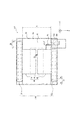
- FIG. 3 is a diagram showing an example of a usage state of the antenna shown in FIG.
- FIG. 4 is a diagram showing another example of the usage state of the antenna shown in FIG.
- FIG. 5 is a plan view of the antenna according to another embodiment of the present disclosure.
- FIG. 6 is a diagram showing an example of a usage state of the antenna shown in FIG.
- FIG. 7 is a plan view of the antenna according to still another embodiment of the present disclosure.
- FIG. 8 is a plan view of the antenna according to still another embodiment of the present disclosure.
- FIG. 9 is a plan view of the antenna according to still another embodiment of the present disclosure.
- FIG. 10 is a plan view of the antenna according to still another embodiment of the present disclosure.
- FIG. 11 is a block diagram of a wireless communication device according to an embodiment of the present disclosure.
- FIG. 12 is a cross-sectional view of the wireless communication device shown in FIG.
- FIG. 13 is a cross-sectional view of a wireless communication device according to another embodiment of the present disclosure.
- the "dielectric material” may include either a ceramic material or a resin material as a composition.
- Ceramic materials include aluminum oxide sintered body, aluminum nitride sintered body, mulite sintered body, glass-ceramic sintered body, crystallized glass in which crystal components are precipitated in the glass base material, and mica or titanium. Includes microcrystalline sintered body such as aluminum acid.
- the resin material includes a cured product such as an epoxy resin, a polyester resin, a polyimide resin, a polyamide-imide resin, a polyetherimide resin, and a liquid crystal polymer.
- the "conductive material” may include any of a metal material, an alloy of the metal material, a cured product of the metal paste, and a conductive polymer as a composition.
- Metallic materials include copper, silver, palladium, gold, platinum, aluminum, chromium, nickel, cadmium lead, selenium, manganese, tin, vanadium, lithium, cobalt, titanium and the like. Alloys include multiple metallic materials.
- the metal paste agent includes a powder of a metal material kneaded with an organic solvent and a binder.
- the binder includes an epoxy resin, a polyester resin, a polyimide resin, a polyamide-imide resin, and a polyetherimide resin.
- the conductive polymer includes a polythiophene-based polymer, a polyacetylene-based polymer, a polyaniline-based polymer, a polypyrrole-based polymer, and the like.
- the XYZ coordinate system is adopted.
- the X-axis positive direction and the X-axis negative direction are not particularly distinguished, the X-axis positive direction and the X-axis negative direction are collectively referred to as "X direction”.
- the Y-axis positive direction and the Y-axis negative direction are not particularly distinguished, the Y-axis positive direction and the Y-axis negative direction are collectively referred to as "Y direction”.
- Z direction and the Z-axis negative direction are not particularly distinguished, the Z-axis positive direction and the Z-axis negative direction are collectively referred to as "Z direction”.
- the first direction is shown as the X direction.
- the second direction is shown as the Z direction.
- the third direction is shown as the Y direction.
- the first plane is shown as the XZ plane.
- the second plane is shown as the XY plane.
- the first direction does not have to be orthogonal to the second direction.
- the first direction may intersect the second direction.
- the third direction does not have to be orthogonal to the XZ plane shown as the first plane.
- the third direction may intersect the first plane.
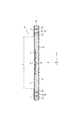
- FIG. 1 is a plan view of the antenna 10 according to the embodiment of the present disclosure.
- FIG. 2 is a cross-sectional view of the antenna 10 along the line L1-L1 shown in FIG.
- the antenna 10 includes a base 20, a first conductor 30, a second conductor 33, a third conductor 40, a fourth conductor 50, a feeder line 60, and a reinforcing member 70. And include.
- the first conductor 30 and the second conductor 33 are also referred to as anti-conductors.
- the antenna 10 may further include a connecting component 80.
- Each of the first conductor 30, the second conductor 33, the third conductor 40, the fourth conductor 50, and the feeder line 60 contains a conductive material.
- the first conductor 30, the second conductor 33, the third conductor 40, the fourth conductor 50, and the feeder line 60 may contain the same conductive material or may contain different conductive materials.
- the antenna 10 can exhibit an artificial magnetic wall characteristic (Artificial Magnetic Conductor Character) with respect to an electromagnetic wave of a predetermined frequency incident on a surface on which the third conductor 40 is located from the outside.
- an artificial magnetic wall characteristic Artificial Magnetic Conductor Character
- the "artificial magnetic wall characteristic” means the characteristic of the surface where the phase difference between the incident wave and the reflected wave at one resonance frequency is 0 degrees.
- the antenna 10 may have an operating frequency in the vicinity of at least one of at least one resonance frequency.
- the phase difference between the incident wave and the reflected wave becomes smaller than the range from ⁇ 90 degrees to +90 degrees in the operating frequency band.
- the region A of the antenna 10 may have flexibility.
- the region A of the antenna 10 may be bent in the X direction according to the arrangement location of the antenna 10 and the like. Region A is a partial region of the antenna 10 in the X direction.
- the region A may be a region including the third conductor 40.
- the region A may be a region that does not include the first conductor 30 and the second conductor 33.
- the region A of the antenna 10 may be bent in the X direction in the positive direction of the Z axis as shown in FIG. 3 described later, or bent in the negative direction of the Z axis as shown in FIG. 4 described later. May be done.
- the antenna 10 may be configured as a flexible wiring board (FPC: Flexible Printed Circuit).
- the substrate 20 contains a dielectric material.
- the substrate 20 may have any shape depending on the shape of the third conductor 40 and the like.
- the substrate 20 may have a substantially rectangular parallelepiped shape.
- the relative permittivity of the substrate 20 may be appropriately adjusted according to the desired operating frequency of the antenna 10.
- the substrate 20 includes an upper surface 21 and a lower surface 22.
- the upper surface 21 is a plane located on the Z-axis positive direction side of the two planes substantially parallel to the XY plane included in the substrate 20.
- the lower surface 22 is a plane located on the negative side of the Z axis of the two planes substantially parallel to the XY plane included in the substrate 20.
- the first conductor 30 is located on the negative direction side of the X axis with respect to the second conductor 33.
- the first conductor 30 may be located at the end of the substrate 20 on the negative direction side of the X axis.
- the first conductor 30 is along the Y direction.
- the first conductor 30 includes at least one first connecting conductor 31 and a first conductor layer 32.
- the first connecting conductor 31 and the first conductor layer 32 may contain the same conductive material or may contain different conductive materials.
- the plurality of first connecting conductors 31 may be arranged in the Y direction with a space.
- the plurality of first connecting conductors 31 may be arranged in the Y direction at substantially equal intervals.
- the plurality of first connecting conductors 31 may be arranged in two rows in the Y direction. However, the first connecting conductors 31 may be arranged in one row in the Y direction, or may be arranged in three or more rows in the Y direction.
- the first connecting conductor 31 extends from the fourth conductor 50 to the first conductor layer 32 along the Z direction.
- the first connecting conductor 31 includes two ends. In the first connecting conductor 31, one end of the first connecting conductor 31 is electrically connected to the fourth conductor 50, and the other end of the first connecting conductor 31 is electrically connected to the first conductor layer 32. It may be configured to be.
- the first connecting conductor 31 may be a through-hole conductor, a via conductor, or the like.
- the first conductor layer 32 is located on the upper surface 21 of the substrate 20.
- the first conductor layer 32 may have a flat plate shape.
- the first conductor layer 32 may have a substantially rectangular shape.
- the first conductor layer 32 includes two surfaces substantially parallel to the XY plane. One of the two surfaces faces the fourth conductor 50.
- the first conductor layer 32 is configured to be electrically connected to the third conductor 40.
- the surface of the first conductor layer 32 that is substantially parallel to the XY plane and that faces the fourth conductor 50 is electrically connected to the end of the first connecting conductor 31. It may be configured to be.
- the first conductor layer 32 is configured so that a part of the end portion of the first conductor layer 32 on the positive direction side of the X axis is electrically connected to the fifth conductor 41 described later of the third conductor 40. You may be.
- the second conductor 33 faces the first conductor 30 in the X direction.
- the second conductor 33 is located on the positive side of the X-axis with respect to the first conductor 30.
- the second conductor 33 may be located at the end of the substrate 20 on the positive direction side of the X axis.
- the second conductor 33 is along the Y direction.
- the second conductor 33 includes at least one second connecting conductor 34 and a second conductor layer 35.
- the second connecting conductor 34 and the second conductor layer 35 may contain the same conductive material or may contain different conductive materials.
- the plurality of second connecting conductors 34 may be arranged in the Y direction with a space.
- the plurality of second connecting conductors 34 may be arranged in the Y direction at substantially equal intervals.
- the second connecting conductors 34 may be arranged in two rows in the Y direction. However, the second connecting conductors 34 may be arranged in one row in the Y direction, or may be arranged in three or more rows in the Y direction.
- the second connecting conductor 34 extends from the fourth conductor 50 to the second conductor layer 35 along the Z direction.
- the second connecting conductor 34 includes two ends. In the second connecting conductor 34, one end of the second connecting conductor 34 is electrically connected to the fourth conductor 50, and the other end of the second connecting conductor 34 is electrically connected to the second conductor layer 35. It may be configured to be.
- the second connecting conductor 34 may be a through-hole conductor, a via conductor, or the like.
- the second conductor layer 35 is located on the upper surface 21 of the substrate 20.
- the second conductor layer 35 may have a flat plate shape.
- the second conductor layer 35 may have a substantially rectangular shape.
- the second conductor layer 35 includes two surfaces substantially parallel to the XY plane. One of the two surfaces faces the fourth conductor 50.
- the second conductor layer 35 may include an opening 35a. A part of the connecting component 80 is located in the opening 35a.
- the second conductor layer 35 is configured to be electrically connected to the third conductor 40.
- the surface of the second conductor layer 35 that is substantially parallel to the XY plane and that faces the fourth conductor is electrically connected to the end of the second connecting conductor 34. It may be configured so as to.
- the second conductor layer 35 is configured so that a part of the end portion of the second conductor layer 35 on the negative direction side of the X axis is electrically connected to the sixth conductor 42 described later of the third conductor 40. You may be.
- the third conductor 40 is along the X direction.
- the third conductor 40 may extend along the XY plane.
- the third conductor 40 is located between the first conductor 30 and the second conductor 33.
- the third conductor 40 includes a fifth conductor 41, a sixth conductor 42, and an inner conductor 43.
- the fifth conductor 41, the sixth conductor 42, and the inner conductor 43 may contain the same conductive material, or may contain different conductive materials.
- the fifth conductor 41 and the sixth conductor 42 are located on the upper surface 21 of the substrate 20. A part of the fifth conductor 41 and a part of the sixth conductor 42 may be located in the substrate 20.
- the fifth conductor 41 and the sixth conductor 42 may have a substantially rectangular shape.
- the fifth conductor 41 is configured to be electrically connected to the first conductor layer 32 of the first conductor 30.
- the end of the fifth conductor 41 on the negative direction side of the X axis may be configured to be electrically connected to the first conductor layer 32.
- the end portion of the fifth conductor 41 on the negative direction side of the X axis may be integrated with a part of the end portion of the first conductor layer 32.
- the sixth conductor 42 is configured to be electrically connected to the second conductor layer 35 of the second conductor 33.
- the end of the sixth conductor 42 on the positive direction side of the X axis may be configured to be electrically connected to the second conductor layer 35.
- the end of the sixth conductor 42 on the positive direction side of the X axis may be integrated with a part of the end of the first conductor layer 32.
- the end of the fifth conductor 41 on the positive side of the X-axis and the end of the sixth conductor 42 on the negative side of the X-axis face each other.
- a gap S1 is located between the end of the fifth conductor 41 on the positive side of the X-axis and the end of the sixth conductor 42 on the negative direction of the X-axis.
- the fifth conductor 41 and the sixth conductor 42 have a gap S1 located between the end of the fifth conductor 41 on the positive direction side of the X axis and the end of the sixth conductor 42 on the negative direction of the X axis.
- the width of the gap S1 in the X direction may be appropriately adjusted according to the desired operating frequency of the antenna 10.
- the inner conductor 43 is located in the substrate 20.
- the inner conductor 43 is not electrically connected to the fifth conductor 41 and the sixth conductor 42.
- the inner conductor 43 is located on the negative side of the Z axis with respect to the fifth conductor 41 and the sixth conductor 42.
- the inner conductor 43 may have a substantially rectangular shape.
- the inner conductor 43 is configured to capacitively connect the fifth conductor 41 and the sixth conductor 42.
- the inner conductor 43 is separated from the fifth conductor 41 and the sixth conductor 42.
- a portion of the inner conductor 43 may overlap a portion of the fifth conductor 41.
- the other part of the inner conductor 43 may overlap the part of the sixth conductor 42.
- the inner conductor 43 can be capacitively connected to the fifth conductor 41 and the sixth conductor 42 by overlapping a part of the fifth conductor 41 and a part of the sixth conductor 42 in the XY plane.
- the third conductor 40 is configured to capacitively connect the first conductor 30 and the second conductor 33.
- the fifth conductor 41 is configured to be electrically connected to the first conductor layer 32 of the first conductor 30.
- the sixth conductor 42 is configured to be electrically connected to the second conductor layer 35 of the second conductor 33.
- the fifth conductor 41 and the sixth conductor 42 can be capacitively connected by the gap S1 and the inner conductor 43.
- the fourth conductor 50 is along the X direction.
- the fourth conductor 50 may extend along the XY plane.
- the fourth conductor 50 is separated from the third conductor 40.
- the fourth conductor 50 may face the third conductor 40.
- the fourth conductor 50 may be located on the lower surface 22 of the substrate 20. A part of the fourth conductor 50 may be located in the substrate 20.
- the fourth conductor 50 may have any shape depending on the shape of the third conductor 40.
- the fourth conductor 50 may have a substantially rectangular shape.
- the fourth conductor 50 is configured to be electrically connected to the first conductor 30 and the second conductor 33.
- a part of the fourth conductor 50 on the negative direction side of the X axis is configured to be electrically connected to the end of the first connecting conductor 31 of the first conductor 30.
- a part of the fourth conductor 50 on the positive direction side of the X axis is configured to be electrically connected to the end of the second connecting conductor 34 of the second conductor 33.
- the fourth conductor 50 is configured to provide a reference potential in the antenna 10.
- the fourth conductor 50 may be configured to be electrically connected to the ground of the device including the antenna 10.
- a part of the fourth conductor 50 may be configured to be electrically connected to the ground conductor 91 of the circuit board 90.
- Various components of the device including the antenna 10 may be located on the negative side of the fourth conductor 50 on the Z axis.
- the antenna 10 can maintain the radiation efficiency at the operating frequency by having the above-mentioned artificial magnetic wall characteristics even when the various parts are located on the Z-axis negative direction side of the fourth conductor 50.
- the feeder line 60 is configured to be electromagnetically connected to the third conductor 40.
- the "electromagnetic connection” may be an electrical connection or a magnetic connection.
- one end of the feeder line 60 is configured to be electrically connected to the sixth conductor 42 of the third conductor 40.
- the other end of the feeder line 60 is configured to be electrically connected to the connecting component 80.
- the feeder line 60 may be located on the upper surface 21 of the substrate 20. A part of the feeder line 60 may be located in the substrate 20.
- the feeder line 60 is configured to supply electric power from the RF module or the like to the third conductor 40 via the connecting component 80 when the electromagnetic wave is radiated by the antenna 10.
- the power feeding line 60 is configured to supply the electric power from the third conductor 40 to the RF module or the like via the connecting component 80.
- a loop current that flows in a loop through the first conductor 30, the second conductor 33, the third conductor 40, and the fourth conductor 50 can be generated.
- the first conductor 30 can be seen as an electric wall extending in the YZ plane on the negative direction side of the X axis
- the second conductor 33 can be seen as an electric wall spreading in the YZ plane on the positive direction side of the X axis.
- no conductor or the like is located on the Y-axis positive direction side and the Y-axis negative direction side.
- the Y-axis positive direction side and the Y-axis negative direction side are electrically open. Since the Y-axis positive direction side and the Y-axis negative direction side are electrically opened, the XZ plane on the Y-axis positive direction side and the XY plane on the Y-axis negative direction side are magnetic walls from the loop current. Can be seen as.
- the antenna 10 has artificial magnetic wall characteristics with respect to electromagnetic waves of a predetermined frequency incident on the upper surface 21 of the substrate 20 from the positive direction side of the Z axis. Is shown.
- the reinforcing member 70 is configured to protect at least a part of the first conductor 30 and the second conductor 33.
- the reinforcing member 70 is located in at least a part of the first conductor 30 and the second conductor 33.
- the reinforcing member 70 includes a first reinforcing member 71 and a second reinforcing member 72.
- the reinforcing member 70 may include at least one of the first reinforcing member 71 and the second reinforcing member 72, depending on the arrangement location of the antenna 10.
- Each of the first reinforcing member 71 and the second reinforcing member 72 contains a dielectric material.
- the first reinforcing member 71 and the second reinforcing member 72 may contain the same dielectric material or may contain different dielectric materials.
- the first reinforcing member 71 may be located at least a part of the first conductor 30.
- the first reinforcing member 71 may be located on the first conductor layer 32.
- the first reinforcing member 71 may be located on the first conductor layer 32 so as to be located at the end of the first connecting conductor 31.
- the first reinforcing member 71 may spread on the first conductor layer 32 so as to be located at the end of the plurality of first connecting conductors 31.
- the area of the first reinforcing member 71 in the XY plane may be smaller than the area of the first conductor layer 32 in the XY plane.
- the area of the first reinforcing member 71 in the XY plane may be an area capable of covering the ends of the plurality of first connecting conductors 31.
- the shape of the first reinforcing member 71 may be a shape corresponding to the arrangement of the first connecting conductors 31 in the XY plane. For example, when a plurality of first connecting conductors 31 are arranged in two rows in the Y direction, the shape of the first reinforcing member 71 may be substantially rectangular.
- the material of the first reinforcing member 71 and the thickness of the first reinforcing member 71 in the Z direction may be appropriately selected in consideration of the stress applied to the first conductor 30.
- the region A of the antenna 10 can bend in the positive direction of the Z axis in the X direction. Since the first reinforcing member 71 is located at least a part of the first conductor 30, the degree of deformation of the first conductor 30 can be reduced when the region A of the antenna 10 is bent. By reducing the degree of deformation of the first conductor 30, the stress applied to the first connecting conductor 31 can be reduced. By reducing the stress applied to the first connecting conductor 31, the possibility that the first connecting conductor 31 is damaged can be reduced. Further, by locating the first reinforcing member 71 on the first conductor layer 32 so as to be located at the end of the first connecting conductor 31, the stress applied to the first connecting conductor 31 can be further reduced. By further reducing the stress applied to the first connecting conductor 31, the possibility of damage to the first connecting conductor 31 can be further reduced.
- the second reinforcing member 72 may be located at least a part of the second conductor 33.
- the second reinforcing member 72 may be located on the second conductor layer 35.
- the second reinforcing member 72 may be located on the second conductor layer 35 so as to be located at the end of the second connecting conductor 34.
- the second reinforcing member 72 may spread on the second conductor layer 35 so as to be located at the end of the plurality of second connecting conductors 34.
- the area of the second reinforcing member 72 in the XY plane may be smaller than the area of the second conductor layer 35 in the XY plane.
- the area of the second reinforcing member 72 in the XY plane may be an area capable of covering the ends of the plurality of second connecting conductors 34.
- the shape of the second reinforcing member 72 may be a shape corresponding to the arrangement of the second connecting conductor 34 in the XY plane. For example, when a plurality of second connecting conductors 34 are arranged in two rows in the Y direction, the shape of the second reinforcing member 72 may be substantially rectangular.
- the material of the second reinforcing member 72 and the thickness of the second reinforcing member 72 in the Z direction may be appropriately selected in consideration of the stress applied to the second conductor 33.
- the region A of the antenna 10 can bend in the negative direction of the Z axis in the X direction.
- the configuration shown in FIG. 4 corresponds to a cross-sectional view taken along the line L2-L2 shown in FIG.
- the second reinforcing member 72 may be located at least a part of the second conductor 33, so that the second connecting conductor 34 may be damaged in the same manner as the first reinforcing member 71. Can be reduced. Further, by locating the second reinforcing member 72 on the second conductor layer 35 so as to be located at the end of the second connecting conductor 34, the second connecting conductor 34 is damaged in the same manner as the first reinforcing member 71. The possibility can be further reduced.
- the second reinforcing member 72 may be positioned so as to overlap the connecting component 80 on the XY plane.
- the second reinforcing member 72 may be positioned so as to cover the opening 35a of the second conductor layer 35.
- the connecting component 80 is aligned with the second connecting conductor 34 in the Y direction.
- the connecting component 80 may be located on the positive side of the Y-axis with respect to the second connecting conductor 34.
- the connection component 80 is configured to electrically connect the feeder line 60 and the circuit board 90.
- the connecting component 80 may be any component.
- the connection component 80 may be a surface mount type (SMT: Surface Mount Technology) connector.
- the circuit board 90 can be one of the components of the device including the antenna 10.
- the circuit board 90 may be a multilayer board.
- the circuit board 90 is located on the negative direction side of the Z axis of the antenna 10. In the configuration shown in FIG. 4, a part of the antenna 10 may overlap a part of the circuit board 90 in the XY plane. However, as shown in FIG. 12 described later, all of the antennas 10 may overlap with the circuit board 90 in the XY plane.
- the circuit board 90 overlaps with a part of the antenna 10, for example, it may be configured as a printed wiring board (PCB: Printed circuit board).
- the circuit board 90 may be configured as a flexible wiring board when it overlaps with all of the antennas 10, for example.
- the circuit board 90 includes a ground conductor 91, an insulating layer 92, an insulating layer 93, a wiring layer 94, and a solder 95.
- the ground conductor 91 contains a conductive material.
- the ground conductor 91 is located on the circuit board 90 on the positive side of the Z axis.
- the ground conductor 91 is configured to be electrically connected to the ground of the device including the antenna 10.
- Each of the insulating layer 92 and the insulating layer 93 contains an arbitrary insulating material.
- the insulating layer 92 is located on the negative side of the ground conductor 91 in the negative direction of the Z axis.
- the insulating layer 93 is located on the negative side of the wiring layer 94 in the negative direction of the Z axis.
- the wiring layer 94 is located between the insulating layer 92 and the insulating layer 93.
- the wiring layer 94 includes a wiring pattern 94A and an insulating layer 94B containing an arbitrary insulating material.
- the wiring pattern 94A includes a conductive material.
- the wiring pattern 94A is configured to be electrically connected to the RF module.
- Solder 95 is located in a part of the wiring pattern 94A.
- the wiring pattern 94A can be electrically connected to the connecting component 80 by the solder 95.
- the solder 95 is located between the connecting component 80 and the wiring pattern 94A.
- the solder 95 is configured to electrically connect the connecting component 80 and the wiring pattern 94A.
- the antenna 10 includes a reinforcing member 70 located in at least a part of the first conductor 30 and the second conductor 33.
- the region A of the antenna 10 is bent by the first reinforcing member 71, the degree of deformation of the first conductor 30 can be reduced.
- the possibility of damage to the first connecting conductor 31 can be reduced.
- the region A of the antenna 10 is bent by the second reinforcing member 72, the degree of deformation of the second conductor 33 can be reduced.
- the degree of deformation of the second conductor 33 By reducing the degree of deformation of the second conductor 33, the possibility of damage to the second connecting conductor 34 can be reduced. Therefore, according to the present embodiment, a new antenna 10 having excellent long-term reliability can be provided.
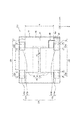
- FIG. 5 is a plan view of the antenna 110 according to another embodiment of the present disclosure.
- FIG. 6 is a diagram showing an example of a usage state of the antenna 110 shown in FIG. The configuration shown in FIG. 6 corresponds to a cross-sectional view taken along the line L3-L3 shown in FIG.
- the antenna 110 includes a base 20, a first conductor 30, a second conductor 33, a third conductor 40, a fourth conductor 50, a feeder line 60, and a reinforcing member 170.
- the antenna 110 may further include a connecting component 180.
- the antenna 110 can exhibit artificial magnetic wall characteristics with respect to electromagnetic waves of a predetermined frequency incident on the surface on which the third conductor 40 is located from the outside, in the same manner as or similar to the antenna 10. At least a portion of the antenna 110 may be as flexible as or similar to the antenna 10. The antenna 110 may be configured as a flexible wiring board.
- the circuit board 190 is located in a part of the antenna 110.
- the circuit board 190 is located on the Z-axis positive direction side of the antenna 110.
- the reinforcing member 170 is configured to protect at least a part of the first conductor 30 and the second conductor 33.
- the reinforcing member 170 is located in at least a part of the first conductor 30 and the second conductor 33.
- the reinforcing member 170 includes a first reinforcing member 71 and a second reinforcing member 172.
- the reinforcing member 170 may include at least one of the first reinforcing member 71 and the second reinforcing member 172, depending on the arrangement location of the antenna 10.
- the second reinforcing member 172 includes a dielectric material.
- the second reinforcing member 172 may be located at least a part of the second conductor 33.
- the second reinforcing member 172 may be located on the second conductor layer 35. However, the second reinforcing member 172 does not have to be located in the portion of the second conductor layer 35 where the connecting component 80 and the circuit board 190 are located.
- Other configurations of the second reinforcing member 172 are the same as or similar to those of the second reinforcing member 72 as shown in FIG.
- the region A of the antenna 110 can bend in the negative direction of the Z axis. Similar to the second reinforcing member 72, when the region A of the antenna 110 is bent, the second connecting conductor 34 may be damaged because the second reinforcing member 172 is located at least a part of the second conductor 33. Can be reduced. Further, similarly to the second reinforcing member 72, since the second reinforcing member 172 is located above the end portion of the second connecting conductor 34, the possibility that the second connecting conductor 34 is damaged can be further reduced.
- the connecting component 180 is aligned with the second connecting conductor 34 in the Y direction.
- the connecting component 180 may be located on the positive side of the Y-axis with respect to the second connecting conductor 34.
- the connection component 180 is configured to electrically connect the feeder line 60 and the circuit board 190.
- the connecting component 180 may be any component.
- the connector 180 may be a surface mount type connector.
- the circuit board 190 can be one of the components of the device including the antenna 110.
- the circuit board 190 may be a multilayer board.
- the circuit board 190 is located on the Z-axis positive direction side of the antenna 110. In the XY plane, a part of the circuit board 190 may overlap with a part of the antenna 110 on the positive side of the X axis.
- the circuit board 190 includes an insulating layer 191, an insulating layer 192, a wiring layer 193, and a solder 194.
- Each of the insulating layer 191 and the insulating layer 192 contains an arbitrary insulating material.
- the insulating layer 191 is the lowest layer.
- the insulating layer 191 is located above the antenna 110.
- the insulating layer 192 is located on the Z-axis positive direction side of the wiring layer 193.
- the wiring layer 193 is located between the insulating layer 191 and the insulating layer 192.
- the wiring layer 193 includes a wiring pattern 193A and an insulating layer 193B containing any insulating material.
- the wiring pattern 193A includes a conductive material.
- the wiring pattern 193A is configured to be electrically connected to the RF module.
- Solder 194 is located in a part of the wiring pattern 193A.
- the wiring pattern 193A can be electrically connected to the connecting component 180 by the solder 194.
- Solder 194 is located between the connecting component 180 and the wiring pattern 193A.
- the solder 194 is configured to electrically connect the connecting component 180 and the wiring pattern 193A.
- FIG. 7 is a plan view of the antenna 210 according to still another embodiment of the present disclosure.
- the antenna 210 includes a base 20, a first conductor 230, a second conductor 233, a third conductor 40, a fourth conductor 50, a feeder line 60, and a reinforcing member 270.
- the antenna 210 may further include a connecting component 80.
- Each of the first conductor 230 and the second conductor 233 contains a conductive material.
- the first conductor 230, the second conductor 233, the third conductor 40, the fourth conductor 50, and the feeder line 60 may contain the same conductive material or may contain different conductive materials.
- the antenna 210 can exhibit artificial magnetic wall characteristics with respect to electromagnetic waves of a predetermined frequency incident on the surface on which the third conductor 40 is located from the outside, in the same manner as or similar to the antenna 10.
- At least a part of the antenna 210 may have flexibility.
- the region A of the antenna 210 may be bent in the X direction according to the arrangement location of the antenna 210 and the like.
- the region B of the antenna 210 may be bent in the Y direction.
- the region B of the antenna 210 may be bent in the positive direction of the Z axis in the Y direction, or may be bent in the negative direction of the Z axis.
- Region B is a partial region of the antenna 210 in the Y direction. Part or all of area B may overlap some or all of area A.
- the region B may be a region including at least a part of the third conductor 40.
- the region B may be a region that does not include the first connecting conductor 31 and the second connecting conductor 34.
- the antenna 210 may be configured as a flexible wiring board.
- a circuit board 90 is located in a part of the antenna 210, similar to the configuration shown in FIG. Similar to the configuration shown in FIG. 4, the circuit board 90 is located on the negative Z-axis side of the antenna 210.
- the first conductor 230 includes a first connecting conductor set 231A, a first connecting conductor set 231B, and a first conductor layer 32.
- first connecting conductor set 231A and the first connecting conductor set 231B are not particularly distinguished, they are collectively referred to as "first connecting conductor set 231".
- the first connecting conductor set 231 includes at least one first connecting conductor 31.
- the plurality of first connecting conductors 31 may be arranged in two rows in the Y direction.
- the first connecting conductor set 231A and the first connecting conductor set 231B are separated from each other with a first interval in the Y direction.
- the first interval is wider than the interval in which the first connecting conductors 31 are lined up in the Y direction in the first connecting conductor set 231.
- the first interval may be appropriately set in consideration of the curvature of the region B of the antenna 210 in the Y direction.
- the first connecting conductor set 231A is located near the corners on the negative X-axis side and the negative Y-axis side of the four corners of the fifth conductor 41.
- the first connecting conductor set 231B is located near the corners on the negative X-axis side and the positive Y-axis side of the four corners of the fifth conductor 41.
- the second conductor 233 includes a second connecting conductor set 234A, a second connecting conductor set 234B, and a second conductor layer 35.
- second connecting conductor set 234" when the second connecting conductor set 234A and the second connecting conductor set 234B are not particularly distinguished, they are collectively referred to as "second connecting conductor set 234".
- the second connecting conductor set 234 includes at least one second connecting conductor 34.
- the plurality of second connecting conductors 34 may be arranged in two rows in the Y direction.
- the second connecting conductor set 234A and the second connecting conductor set 234B are separated from each other with a second interval in the Y direction.
- the second interval may be the same as the first interval or may be different from the first interval.
- the second interval is wider than the interval in which the second connecting conductors 34 are lined up in the Y direction in the second connecting conductor set 234.
- the second interval may be appropriately set in consideration of the curvature of the region B of the antenna 210 in the Y direction.
- the second connecting conductor set 234A is located near the corners on the positive side of the X-axis and the negative side of the Y-axis among the four corners of the sixth conductor 42.
- the second connecting conductor set 234B is located near the corners on the positive X-axis side and the positive Y-axis side of the four corners of the sixth conductor 42.
- the reinforcing member 270 is configured to protect at least a part of the first conductor 230 and the second conductor 233.
- the reinforcing member 270 is located in at least a part of the first conductor 230 and the second conductor 233.
- the reinforcing member 270 includes a first reinforcing member 271 including a third reinforcing member 273A and a third reinforcing member 273B, and a second reinforcing member 272 including a fourth reinforcing member 274A and a fourth reinforcing member 274B.
- the reinforcing member 270 may include at least one of the third reinforcing member 273A, the third reinforcing member 273B, the fourth reinforcing member 274A, and the fourth reinforcing member 274B, depending on the arrangement location of the antenna 210 and the like.
- the third reinforcing member 273A and the third reinforcing member 273B are not particularly distinguished, these are described as “third reinforcing member 273".
- the fourth reinforcing member 274A and the fourth reinforcing member 274B are not particularly distinguished, these are described as "fourth reinforcing member 274".
- the third reinforcing member 273 and the fourth reinforcing member 274 include a dielectric material.
- the third reinforcing member 273A, the third reinforcing member 273B, the fourth reinforcing member 274A, and the fourth reinforcing member 274B may contain the same dielectric material or may contain different dielectric materials.
- the third reinforcing member 273A and the third reinforcing member 273B are located on the first conductor layer 32, respectively.
- the third reinforcing member 273A and the third reinforcing member 273B are separated from each other in the Y direction.
- the third reinforcing member 273A is located in the first connecting conductor set 231A.
- the third reinforcing member 273A may be located on the first conductor layer 32 so as to be located at the end of the first connecting conductor 31 of the first connecting conductor set 231A.
- the third reinforcing member 273A may extend on the first conductor layer 32 so as to be located at the ends of the plurality of first connecting conductors 31 of the first connecting conductor set 231A.
- the third reinforcing member 273B is located in the first connecting conductor set 231B.
- the third reinforcing member 273B may be located on the first conductor layer 32 so as to be located at the end of the first connecting conductor 31 of the first connecting conductor set 231B.
- the third reinforcing member 273B may extend on the first conductor layer 32 so as to be located at the ends of the plurality of first connecting conductors 31 of the first connecting conductor set 231B.
- the area of the third reinforcing member 273 in the XY plane may be an area capable of covering the end portion of the first connecting conductor 31 included in the first connecting conductor set 231.
- the shape of the third reinforcing member 273 may be a shape corresponding to the arrangement of the first connecting conductors 31 in the first connecting conductor set 231 in the XY plane. For example, when a plurality of first connecting conductors 31 are arranged in two rows in the Y direction in the first connecting conductor set 231, the shape of the third reinforcing member 273 may be substantially rectangular.
- the material of the third reinforcing member 273 and the thickness in the Z direction may be appropriately selected in consideration of the stress applied to the first conductor 230.
- the region A of the antenna 210 can bend in the positive direction of the Z axis, similar to the configuration shown in FIG.
- the stress applied to the first connecting conductor 31 can be reduced, and the possibility that the first connecting conductor 31 is damaged can be reduced.
- Region B of the antenna 210 can be bent in the Y direction. When the region B of the antenna 210 is bent, the stress applied to the first connecting conductor 31 is reduced by locating the third reinforcing member 273 in the first connecting conductor set 231 and the first connecting conductor 31 may be damaged. Can be reduced.
- the fourth reinforcing member 274A and the fourth reinforcing member 274B are located on the second conductor layer 35, respectively.
- the fourth reinforcing member 274A and the fourth reinforcing member 274B are separated in the Y direction.
- the fourth reinforcing member 274A is located in the second connecting conductor set 234A.
- the fourth reinforcing member 274A may be located on the second conductor layer 35 so as to be located at the end of the second connecting conductor 34 of the second connecting conductor set 234A.
- the fourth reinforcing member 274A may extend on the second conductor layer 35 so as to be located at the ends of the plurality of second connecting conductors 34 of the second connecting conductor set 234A.
- the fourth reinforcing member 274B is located in the second connecting conductor set 234B.
- the fourth reinforcing member 274B may be located on the second conductor layer 35 so as to be located at the end of the second connecting conductor 34 of the second connecting conductor set 234B.
- the fourth reinforcing member 274B may extend over the second conductor layer 35 so as to be located at the ends of the plurality of second connecting conductors 34 of the second connecting conductor set 234B.
- the area of the fourth reinforcing member 274 in the XY plane may be an area capable of covering the ends of a plurality of second connecting conductors 34 included in the second connecting conductor set 234.
- the shape of the fourth reinforcing member 274 may be a shape corresponding to the arrangement of the second connecting conductor 34 in the XY plane in the second connecting conductor set 234. For example, when a plurality of second connecting conductors 34 are arranged in two rows in the Y direction in the second connecting conductor set 234, the shape of the fourth reinforcing member 274 may be substantially rectangular.
- the material of the fourth reinforcing member 274 and the thickness in the Z direction may be appropriately selected in consideration of the stress applied to the second conductor 233.
- the possibility of damaging the second connecting conductor 34 of the second connecting conductor set 234 can be reduced in the same manner as or similar to the third reinforcing member 273. .. Further, when the region B of the antenna 210 is bent in the Y direction, the stress applied to the second connecting conductor 34 is reduced by locating the fourth reinforcing member 274 in the second connecting conductor set 234, and the second connecting conductor 34 Can be reduced from being damaged.
- the fourth reinforcing member 274B may be positioned so as to overlap the connecting component 80 on the XY plane when the circuit board 90 is located on the negative direction side of the Z axis of the antenna 210. Similar to the configuration shown in FIG. 4, by locating the fourth reinforcing member 274B so as to overlap the connecting component 80, the degree of deformation of the connecting component 80 and the solder 95 is reduced, and the connecting component 80 and the solder 95 are damaged. The possibility can be reduced.
- antenna 210 Other configurations and effects of the antenna 210 are the same as or similar to those of the antenna 10 as shown in FIG.
- FIG. 8 is a plan view of the antenna 310 according to still another embodiment of the present disclosure.
- the antenna 310 includes a base 20, a first conductor 230, a second conductor 233, a third conductor 40, a fourth conductor 50, a feeder line 60, and a reinforcing member 370.
- the antenna 310 may further include a connecting component 180.
- the antenna 310 can exhibit artificial magnetic wall characteristics with respect to electromagnetic waves of a predetermined frequency incident on the surface on which the third conductor 40 is located from the outside, in the same manner as or similar to the antenna 10. At least a portion of the antenna 310 may be flexible, similar to the antenna 210. The antenna 310 may be configured as a flexible wiring board.
- a circuit board 190 is located in a part of the antenna 310, similar to the configuration shown in FIGS. 5 and 6. Similar to the configuration shown in FIG. 6, the circuit board 190 is located on the Z-axis positive direction side of the antenna 210.
- the reinforcing member 370 includes a first reinforcing member 271 and a second reinforcing member 372.
- the second reinforcing member 372 includes a fourth reinforcing member 274A and a fourth reinforcing member 374B.
- the fourth reinforcing member 374B contains a dielectric material.
- the fourth reinforcing member 374B may contain the same dielectric material as any of the third reinforcing member 273A, the third reinforcing member 273B, and the fourth reinforcing member 274A, or may contain a different dielectric material.
- the fourth reinforcing member 374B does not have to be located at the portion of the second conductor layer 35 where the connecting component 180 and the circuit board 190 are located.
- Other configurations of the fourth reinforcing member 374B are the same as or similar to those of the fourth reinforcing member 274.
- antenna 310 Other configurations and effects of the antenna 310 are the same as or similar to the antenna 10 as shown in FIG. 1, the antenna 110 as shown in FIG. 5, and / or the antenna 210 as shown in FIG.
- FIG. 9 is a plan view of the antenna 410 according to still another embodiment of the present disclosure.
- the antenna 410 includes a base 20, a first conductor 430, a second conductor 433, a third conductor 440, a fourth conductor 50, a feeder line 60, and a reinforcing member 270.
- the antenna 410 may further include a connecting component 80.
- the antenna 410 may include a connecting component 180 instead of the connecting component 80.
- the antenna 410 may include the reinforcing member 370 instead of the reinforcing member 270.
- Each of the first conductor 430, the second conductor 433 and the third conductor 440 contains a conductive material.
- the first conductor 430, the second conductor 433, the third conductor 440, the fourth conductor 50, and the feeder line 60 may contain the same conductive material or may contain different conductive materials.
- the antenna 410 can exhibit artificial magnetic wall characteristics with respect to electromagnetic waves of a predetermined frequency incident on the surface on which the third conductor 440 is located from the outside.
- At least a part of the antenna 410 may have the same or similar flexibility as the antenna 210.
- the antenna 410 may be configured as a flexible wiring board.
- the first conductor 430 includes a first connecting conductor set 231A, a first connecting conductor set 231B, and a first conductor layer 432.
- the second conductor 433 includes a second connecting conductor set 234A, a second connecting conductor set 234B, and a second conductor layer 435.
- the first conductor layer 432 includes a notch 432a.
- the notch 432a is located near the center of the antenna 410 in the Y direction.
- the second conductor layer 435 includes a notch 435a.
- the notch 435a is located near the center of the antenna 410 in the Y direction.
- the cut portion 432a and the cut portion 435a are along the X direction.
- Other configurations of the first conductor layer 432 and the second conductor layer 435 are the same as or similar to those of the first conductor layer 32 and the second conductor layer 35, respectively.
- the third conductor 440 includes a fifth conductor 441, a sixth conductor 442, and an inner conductor 43.
- the fifth conductor 441 includes a notch 441a.
- the notch portion 441a is located near the center of the antenna 410 in the Y direction.
- the cut portion 441a may be connected to the cut portion 432a of the first conductor layer 432.
- the sixth conductor 442 includes a notch 442a.
- the cut portion 442a is located near the center of the antenna 410 in the Y direction.
- the cut portion 442a may be connected to the cut portion 435a of the second conductor layer 435.
- the cut portion 441a and the cut portion 442a are along the X direction.
- the antenna 410 has a notch 432a in the first conductor layer 432, a notch 435a in the second conductor layer 435, a notch 441a in the fifth conductor 441, and a notch 442a in the sixth conductor 442. Including. Since the antenna 410 includes the notch 432a, the notch 435a, the notch 441a and the notch 442a, the region B of the antenna 410 can easily bend in the Y direction. The widths of the cut portion 432a, the cut portion 435a, the cut portion 441a, and the cut portion 442a in the Y direction may be appropriately set in consideration of the curvature of the region B of the antenna 410 in the Y direction.
- antenna 410 Other configurations and effects of the antenna 410 are the same as or of the antenna 10 as shown in FIG. 1, the antenna 110 as shown in FIG. 5, the antenna 210 as shown in FIG. 7, and / or the antenna 310 as shown in FIG. It is similar.
- FIG. 10 is a plan view of the antenna 510 according to still another embodiment of the present disclosure.
- the antenna 510 includes a base 20, a conductor set 530, 531, 532, 533, a radiation conductor 540, 541, 542, 543, an inner conductor 544, a fourth conductor 50, a feeder line 60, and a reinforcing member 570. including.
- the antenna 510 may further include a connecting component 80.
- the antenna 510 may include a connecting component 180 instead of the connecting component 80.
- Each of the conductor sets 530 to 533, the radiating conductors 540 to 543 and the inner conductor 544 contains a conductive material.
- the conductor sets 530 to 533, the radiating conductors 540 to 543, the inner conductor 544, the fourth conductor 50, and the feeder line 60 may contain the same conductive material or may contain different conductive materials.
- the antenna 510 can exhibit artificial magnetic wall characteristics with respect to electromagnetic waves of a predetermined frequency incident on the surface on which the radiation conductors 540 to 543 are located from the outside.
- the antenna 510 may have flexibility.
- the antenna 510 may be configured as a flexible wiring board.
- the region C of the antenna 510 may be bent in the X direction according to the arrangement location of the antenna 510 and the like.
- Region C is a partial region of the antenna 510 in the X direction.
- the region C may be a region including the radiation conductors 540 to 543.
- the region C may be a region that does not include the conductor sets 530 to 533.
- the antenna 510 may be bent in the positive Z-axis direction, similar to the configuration shown in FIG. 3, or may be bent in the negative Z-axis direction, similar to the configuration shown in FIG. ..
- the region D of the antenna 510 may be bent in the Y direction according to the location where the antenna 510 is arranged.
- the region D is a partial region of the antenna 510 in the Y direction.
- the region D may be a region including the radiation conductors 540 to 543.
- the region D may be a region that does not include the conductor sets 530 to 533.
- the region D of the antenna 510 may be bent in the Y direction in the positive direction of the Z axis or in the negative direction of the Z axis.
- the conductor set 530 and the conductor set 531 are lined up in the Y direction.
- the conductor set 532 and the conductor set 533 are arranged in the Y direction.
- the conductor set 530 and the conductor set 533 are arranged in the X direction.
- the conductor set 531 and the conductor set 532 are arranged in the X direction.
- the conductor sets 530, 531, 532, 533 include connection portions 530a, 531a, 532a, 533a, respectively, and at least one connecting conductor 530b, 531b, 532b, 533b.
- the connecting portions 530a to 533a and the connecting conductors 530b to 533b may contain the same conductive material or may contain different conductive materials.
- the connecting portions 530a to 533a are located on the upper surface 21 of the substrate 20.
- the connecting portions 530a to 533a may have a flat plate shape.
- the connecting portions 530a to 533a may have a substantially rectangular shape.
- a part of the connecting portion 530a is configured to be electrically connected to the corners on the Y-axis negative direction side and the X-axis negative direction side of the four corners of the radiation conductor 540.
- a part of the connecting portion 531a is configured to be electrically connected to the corner portion on the Y-axis positive direction side and the X-axis negative direction side of the four corner portions of the radiation conductor 541.
- a part of the connecting portion 532a is configured to be electrically connected to the corners on the Y-axis positive direction side and the X-axis positive direction side of the four corners of the radiation conductor 542.
- a part of the connecting portion 533a is configured to be electrically connected to the corners on the negative Y-axis side and the positive X-axis side of the four corners of the radiation conductor 543.
- the connecting conductors 530b to 533b extend from the fourth conductor 50 toward the upper surface 21 of the substrate 20 along the Z direction.
- the connecting conductors 530b to 533b each include two ends.
- the connecting conductors 530b to 533b may be configured such that one end of each of the connecting conductors 530b to 533b is electrically connected to the fourth conductor 50.
- the connecting conductors 530b to 533b may be configured such that the other end of each of the connecting conductors 530b to 533b is electrically connected to the connecting portions 530a to 533a.
- the connecting conductors 530b to 533b may be through-hole conductors, via conductors, or the like, respectively.
- the conductor sets 530 to 533 are configured to be electrically connected to different radiation conductors 540 to 543.
- the conductor set 530 is configured to be electrically connected to the radiation conductor 540 by the connecting portion 530a.
- the conductor set 531 is configured to be electrically connected to the radiating conductor 541 by the connecting portion 531a.
- the conductor set 532 is configured to be electrically connected to the radiation conductor 542 by the connecting portion 532a.
- the conductor set 533 is configured to be electrically connected to the radiation conductor 543 by the connecting portion 533a.
- Radiant conductors 540 to 543 spread along the XY plane. Radiant conductors 540 to 543 are separated in the X and Y directions. The radiation conductors 540 to 543 may have a flat plate shape. The radiating conductors 540 to 543 are separated from the fourth conductor 50 in the Z direction. The radiating conductors 540 to 543 may face the fourth conductor 50. Radiant conductors 540 to 543 may be located on the upper surface 21 of the substrate 20.
- the radiant conductor 540 and the radiant conductor 541 are lined up in the Y direction with a gap.
- the radiating conductor 542 and the radiating conductor 543 are arranged in the Y direction with a gap.
- the radiating conductor 540 and the radiating conductor 543 are arranged in the X direction with a gap.
- the radiating conductor 541 and the radiating conductor 542 are arranged in the X direction with a gap.
- the radiating conductors 540 to 533 are configured to be capacitively connected to each other by arranging them in the X and Y directions at intervals from each other.
- the distance between the radiating conductor 540 and the radiating conductor 541 arranged in the Y direction and the distance between the radiating conductor 542 and the radiating conductor 543 arranged in the Y direction may be appropriately adjusted according to the desired operating frequency of the antenna 510.
- the distance between the radiating conductor 540 and the radiating conductor 543 arranged in the X direction and the distance between the radiating conductor 541 and the radiating conductor 542 arranged in the X direction may be appropriately adjusted according to the desired operating frequency of the antenna 510.
- the inner conductor 544 is located in the substrate 20 in the same manner as the inner conductor 43.
- the inner conductor 544 is not electrically connected to the radiating conductors 540-533.
- the inner conductor 544 is located on the negative side of the Z axis with respect to the radiating conductors 540 to 533.
- the inner conductor 544 may have a substantially rectangular shape.
- the inner conductor 544 is configured to capacitively connect the radiating conductors 540 to 533.
- the inner conductor 544 is separated from the radiating conductors 540-533. In the Z direction, a portion of the inner conductor 544 may overlap a portion of the radiation conductors 540-533.
- a part of the inner conductor 544 can be capacitively connected to a part of the radiating conductors 540 to 533 by overlapping a part of the radiating conductors 540 to 533.
- the feeder line 60 is configured to be electromagnetically connected to any of the radiation conductors 540 to 533.
- the feeder line 60 may be configured to be electrically connected to the radiation conductor 542.
- the connecting conductor 530b and the connecting conductor 533b are the first connecting pairs arranged along the X direction.
- the connecting conductor 531b and the connecting conductor 532b form a first connecting pair arranged along the X direction.
- the antenna 510 can resonate at the first frequency along the first current path.
- the first current path includes the connecting conductor 530b and the connecting conductor 533b of the first connecting pair, the radiating conductor 540, the radiating conductor 543, and the fourth conductor 50.
- the first current path includes the connecting conductors 531b and 532b of the first connecting pair, the radiating conductor 541, the radiating conductor 542, and the fourth conductor 50.
- the connecting conductors 530b and 531b can be seen as an electric wall extending in the YZ plane on the negative side of the X axis from the current flowing through the first current path, and the connecting conductor 532b.
- the XZ plane on the positive direction side of the Y axis can be seen as a magnetic wall
- the XZ plane on the negative direction side of the Y axis can be seen as a magnetic wall.
- the current flowing through the first current path is surrounded by two electric walls and two magnetic walls, so that the antenna 510 has a first frequency that is incident on the upper surface 21 of the substrate 20 on which the radiation conductors 540 to 543 are located from the outside. , Shows artificial magnetic wall characteristics for electromagnetic waves polarized along the X direction.
- the connecting conductor 530b and the connecting conductor 531b form a second connecting pair arranged along the Y direction.
- the connecting conductor 532b and the connecting conductor 533b form a second connecting pair arranged along the Y direction.
- Antenna 510 can resonate at a second frequency along the second current path.
- the second current path includes the connecting conductor 530b and the connecting conductor 531b of the second connecting pair, the radiating conductor 540, the radiating conductor 541, and the fourth conductor 50.
- the second current path includes the connecting conductors 532b and 533b of the second connecting pair, the radiating conductor 542, the radiating conductor 543, and the fourth conductor 50.
- the connecting conductors 530b and 533b can be seen as an electric wall extending in the XZ plane on the negative side of the Y axis from the current flowing through the second current path, and the connecting conductors 531b , 532b can be seen as an electric wall extending in the XZ plane on the positive side of the Y axis.
- the YZ plane on the positive direction side of the X axis can be seen as a magnetic wall
- the YZ plane on the negative direction side of the X axis can be seen as a magnetic wall.
- the current flowing through the second current path is surrounded by two electric walls and two magnetic walls, so that the antenna 510 has a second frequency that is incident on the upper surface 21 of the substrate 20 on which the radiation conductors 540 to 543 are located from the outside. , Shows artificial magnetic wall characteristics for electromagnetic waves polarized along the Y direction.
- the reinforcing member 570 is configured to protect at least a part of the conductor sets 530 to 533.
- the reinforcing member 570 is located in at least a part of the conductor sets 530 to 533.
- the reinforcing member 570 includes a first reinforcing member 571 including a third reinforcing member 573A and a third reinforcing member 573B, and a second reinforcing member 572 including a fourth reinforcing member 574A and a fourth reinforcing member 574B.
- the reinforcing member 570 may include at least one of the third reinforcing member 573A, the third reinforcing member 573B, the fourth reinforcing member 574A, and the fourth reinforcing member 574B, depending on the arrangement location of the antenna 510 and the like.
- Each of the third reinforcing member 573A, the third reinforcing member 573B, the fourth reinforcing member 574A and the fourth reinforcing member 574B contains a dielectric material.
- the third reinforcing member 573A, the third reinforcing member 573B, the fourth reinforcing member 574A, and the fourth reinforcing member 574B may contain the same dielectric material or may contain different dielectric materials.
- the third reinforcing member 573A is located in the conductor set 530.
- the third reinforcing member 573A may be located on the connecting portion 530a.
- the third reinforcing member 573A may be located on the connecting portion 530a so as to be located at the end of the connecting conductor 530b.
- the area of the third reinforcing member 573A in the XY plane may be an area capable of covering the end portion of the connecting conductor 530b included in the conductor set 530 on the positive direction side of the Z axis.
- the area of the third reinforcing member 573A in the XY plane may be smaller than the area of the connecting portion 530a in the XY plane.
- the shape of the third reinforcing member 573A may be a shape corresponding to the arrangement of the connecting conductors 530b in the conductor set 530 in the XY plane.
- the material of the third reinforcing member 573A and the thickness in the Z direction may be appropriately selected in consideration of the stress applied to the conductor set 530.
- the degree of deformation of the conductor set 530 can be reduced when the region C of the antenna 510 is bent in the X direction.
- the stress applied to the connecting conductor 530b can be reduced.
- the possibility of damage to the connecting conductor 530b can be reduced.
- the stress applied to the connecting conductor 530b can be further reduced.
- the possibility of damage to the connecting conductor 530b can be further reduced.
- the third reinforcing member 573B is located in the conductor set 531.
- the third reinforcing member 573B may be located on the connecting portion 531a.
- the third reinforcing member 573B may be located on the connecting portion 531a so as to be located at the end of the connecting conductor 531b.
- the area of the third reinforcing member 573B in the XY plane may be an area capable of covering the end portion of the connecting conductor 531b included in the conductor set 531 on the positive direction side of the Z axis.
- the area of the third reinforcing member 573B in the XY plane may be smaller than the area of the connecting portion 531a in the XY plane.
- the shape of the third reinforcing member 573B may be a shape corresponding to the arrangement of the connecting conductors 531b in the conductor set 531 in the XY plane.
- the material of the third reinforcing member 573B and the thickness in the Z direction may be appropriately selected in consideration of the stress applied to the conductor set 531.
- the third reinforcing member 573B By locating the third reinforcing member 573B in the conductor set 531 it is possible to reduce the possibility that the connecting conductor 531b will be damaged, similar to the third reinforcing member 573A. Further, by locating the third reinforcing member 573B on the connecting portion 531a so as to be located at the end of the connecting conductor 531b, the possibility that the connecting conductor 530b is damaged is further reduced as in the case of the third reinforcing member 573A. obtain.
- the fourth reinforcing member 574A is located in the conductor set 533.
- the fourth reinforcing member 574A may be located on the connecting portion 533a.
- the fourth reinforcing member 574A may be located on the connecting portion 533a so as to be located at the end of the connecting conductor 533b.
- the area of the fourth reinforcing member 574A in the XY plane may be an area capable of covering the end portion of the connecting conductor 533b included in the conductor set 533 on the positive direction side of the Z axis.
- the area of the fourth reinforcing member 574A in the XY plane may be smaller than the area of the connecting portion 533a in the XY plane.
- the shape of the fourth reinforcing member 574A may be a shape corresponding to the arrangement of the connecting conductors 533b in the conductor set 533 in the XY plane.
- the material of the fourth reinforcing member 574A and the thickness in the Z direction may be appropriately selected in consideration of the stress applied to the conductor set 533.
- the fourth reinforcing member 574A By locating the fourth reinforcing member 574A on the conductor set 533, the possibility of damage to the connecting conductor 533b can be reduced, similar to the third reinforcing member 573A. Further, by locating the fourth reinforcing member 574A on the connecting portion 533a so as to be located at the end of the connecting conductor 533b, the possibility that the connecting conductor 533b is damaged is further reduced as in the case of the third reinforcing member 573A. obtain.
- the fourth reinforcing member 574B is located in the conductor set 532.
- the fourth reinforcing member 574B may be located on the connecting portion 532a.
- the fourth reinforcing member 574B may be located on the connecting portion 532a so as to be located at the end of the connecting conductor 532b.
- the area of the fourth reinforcing member 574B in the XY plane may be an area capable of covering the end portion of the connecting conductor 532b included in the conductor set 532 on the positive direction side of the Z axis.
- the area of the fourth reinforcing member 574B in the XY plane may be smaller than the area of the connecting portion 532a in the XY plane.
- the shape of the fourth reinforcing member 574B may be a shape corresponding to the arrangement of the connecting conductors 532b in the conductor set 532 in the XY plane.
- the material of the fourth reinforcing member 574B and the thickness in the Z direction may be appropriately selected in consideration of the stress applied to the conductor set 532.
- the fourth reinforcing member 574B By locating the fourth reinforcing member 574B on the conductor set 532, the possibility of damage to the connecting conductor 532b can be reduced, similar to the third reinforcing member 573A. Further, by locating the fourth reinforcing member 574B on the connecting portion 532a so as to be located at the end of the connecting conductor 532b, the possibility that the connecting conductor 532b is damaged is further reduced as in the case of the fourth reinforcing member 574B. obtain.
- the fourth reinforcing member 574B may be positioned so as to overlap the connecting component 80 on the XY plane when the circuit board 90 is located on the negative direction side of the Z axis of the antenna 510.
- the fourth reinforcing member 574B may be positioned so as to cover the opening 35a. Similar to the configuration shown in FIG. 4, by locating the fourth reinforcing member 574B so as to overlap the connecting component 80 on the XY plane, the degree of deformation of the connecting component 80 and the solder 95 is reduced, and the connecting component 80 and the solder 95 are reduced. Can be reduced from being damaged.
- the fourth reinforcing member 574B does not have to be located above the connecting component 180, similar to the configuration shown in FIG. 8, when the antenna 510 includes the connecting component 180 instead of the connecting component 80.
- antenna 510 Other configurations and effects of the antenna 510 are the same as or similar to those of the antenna 10 as shown in FIG.
- FIG. 11 is a block diagram of the wireless communication device 1 according to the embodiment of the present disclosure.
- FIG. 12 is a cross-sectional view of the wireless communication device 1 shown in FIG.
- the wireless communication device 1 includes a wireless communication module 2, a sensor 15, a battery 16, a memory 17, and a controller 18.
- the wireless communication module 2 includes an antenna 10 and an RF module 14.
- the wireless communication device 1 includes a housing 11 and a housing 12, and a circuit board 90.
- the wireless communication module 2 may include any of the antennas 110 to 510 instead of the antenna 10.
- the wireless communication device 1 may include a circuit board 190 instead of the circuit board 90.
- the antenna 10 is located on the circuit board 90.
- the feeder line 60 of the antenna 10 is configured to be electrically connected to the RF module 14 via the connecting component 80 and the circuit board 90.
- the fourth conductor 50 of the antenna 10 may be configured to be electrically connected to the ground conductor 91 of the circuit board 90.
- the ground conductor 91 can spread in the XY plane. In the XY plane, the area of the ground conductor 91 is larger than the area of the fourth conductor 50 of the antenna 10. The length of the ground conductor 91 along the Y direction is longer than the length of the fourth conductor 50 of the antenna 10 along the Y direction. The length of the ground conductor 91 along the X direction is longer than the length of the fourth conductor 50 of the antenna 10 along the X direction.
- the antenna 10 may be located on the end side of the center of the ground conductor 91 in the X direction. The center of the antenna 10 may differ from the center of the ground conductor 91 in the XY plane. The location where the feeder line 60 is electrically connected to the third conductor 40 may differ from the center of the ground conductor 91 in the XY plane.
- a loop current that flows in a loop through the first conductor 30, the second conductor 33, the third conductor 40, and the fourth conductor 50 can be generated at a predetermined frequency. Since the antenna 10 is located on the end side in the X direction from the center of the ground conductor 91, the current path flowing through the ground conductor 91 becomes asymmetric. Since the current path flowing through the ground conductor 91 becomes asymmetric, the polarization component of the radiated wave in the X direction becomes large in the antenna structure including the antenna 10 and the ground conductor 91. By increasing the polarization component of the radiated wave in the X direction, the radiated wave can improve the total radiation efficiency.
- the housing 11 can spread on an XY plane.
- the housing 11 is configured to support other devices.
- the housing 11 may be configured to support the wireless communication device 1.
- the component of the wireless communication device 1 is located on the upper surface 11a of the housing 11.
- the housing 11 may be configured to support the battery 16.
- the battery 16 is located above the upper surface 11a of the housing 11.
- the circuit board 90 and the battery 16 may be arranged in the X direction on the upper surface 11a of the housing 11.
- the first connecting conductor 31 of the antenna 10 is located between the battery 16 and the third conductor 40 of the antenna 10.
- the battery 16 is located on the other side of the first connecting conductor 31 as viewed from the third conductor 40 of the antenna 10.
- the housing 12 can cover other devices.
- the housing 12 includes a lower surface 12a facing the antenna 10.
- the lower surface 12a extends along the XY plane.
- the lower surface 12a is not limited to being flat and may include irregularities.
- the housing 12 may have a conductor member 13.
- the conductor member 13 may be located on the lower surface 12a.
- the conductor member 13 may be located at least one of the inside, the outside and the inside of the housing 12.
- the conductor member 13 may be located on at least one of the upper surface and the side surface of the housing 12.
- the conductor member 13 faces the antenna 10.
- the antenna 10 is configured so that it can be coupled to the conductor member 13 and can radiate electromagnetic waves by using the conductor member 13 as a secondary radiator.
- the capacitive coupling between the antenna 10 and the conductor member 13 can be increased.
- the electromagnetic coupling between the antenna 10 and the conductor member 13 can be increased. This coupling can be a mutual inductance.
- FIG. 13 shows a cross-sectional view of the wireless communication device 101 according to another embodiment of the present disclosure.
- the conductor member 13 as the secondary radiator may be integrally configured with the antenna 10.
- the RF module 14 may be configured to control the power supplied to the antenna 10.
- the RF module 14 is configured to modulate the baseband signal and supply it to the antenna 10.
- the RF module 14 may be configured to modulate the electrical signal received by the antenna 10 into a baseband signal.
- Antenna 10 has a small change in resonance frequency due to the conductor on the circuit board 90 side. By providing the antenna 10 in the wireless communication device 1, the influence of the external environment can be reduced.
- the sensor 15 includes, for example, a speed sensor, a vibration sensor, an acceleration sensor, a gyro sensor, a rotation angle sensor, an angular speed sensor, a geomagnetic sensor, a magnet sensor, a temperature sensor, a humidity sensor, a pressure sensor, an optical sensor, an illuminance sensor, a UV sensor, and a gas sensor.
- Gas concentration sensor Gas concentration sensor, Atmosphere sensor, Level sensor, Smell sensor, Pressure sensor, Air pressure sensor, Contact sensor, Wind sensor, Infrared sensor, Human sensor, Displacement amount sensor, Image sensor, Weight sensor, Smoke sensor, Leakage sensor, It may include a vital sensor, a battery level sensor, an ultrasonic sensor, a GPS (Global Positioning System) signal receiving device, and the like.
- GPS Global Positioning System
- the battery 16 is configured to supply electric power to the wireless communication device 1.
- the battery 16 may be configured to power at least one of the sensor 15, the memory 17, and the controller 18.
- the battery 16 may include at least one of a primary battery and a secondary battery.
- the negative pole of the battery 16 is configured to be electrically connected to the ground terminal of the circuit board 90.
- the negative pole of the battery 16 is configured to be electrically connected to the fourth conductor 50 of the antenna 10.
- the memory 17 may include, for example, a semiconductor memory or the like.
- the memory 17 may be configured to function as the work memory of the controller 18.
- the memory 17 may be included in the controller 18.
- the memory 17 stores a program that describes processing contents that realize each function of the wireless communication device 1, information used for processing in the wireless communication device 1, and the like.
- the controller 18 may include, for example, a processor.
- the controller 18 may include one or more processors.
- the processor may include a general-purpose processor that loads a specific program and executes a specific function, and a dedicated processor specialized for a specific process.
- Dedicated processors may include application-specific ICs. ICs for specific applications are also called ASICs (Application Specific Integrated Circuits).
- the processor may include a programmable logic device.
- the programmable logic device is also called PLD (Programmable Logic Device).
- the PLD may include an FPGA (Field-Programmable Gate Array).
- the controller 18 may be either a SoC (System-on-a-Chip) in which one or a plurality of processors cooperate, or a SiP (System In a Package).
- the controller 18 may store various information or a program for operating each component of the wireless communication device 1 in the memory 17.
- the controller 18 is configured to generate a transmission signal to be transmitted from the wireless communication device 1.
- the controller 18 may be configured to acquire measurement data from, for example, the sensor 15.
- the controller 18 may be configured to generate a transmission signal according to the measurement data.
- the controller 18 may be configured to transmit a baseband signal to the RF module 14 of the wireless communication device 1.
- the configuration according to the present disclosure is not limited to the embodiments described above, and can be modified or changed in many ways.
- the functions and the like included in each component and the like can be rearranged so as not to be logically inconsistent, and a plurality of components and the like can be combined or divided into one.
- first”, “second”, “third”, etc. are examples of identifiers for distinguishing the configuration.
- the configurations distinguished by the descriptions such as “first” and “second” in the present disclosure can exchange numbers in the configurations.
- the first conductor can exchange the identifiers “first” and “second” with the second conductor.
- the exchange of identifiers takes place at the same time.
- the configuration is distinguished.
- the identifier may be deleted.
- the configuration with the identifier removed is distinguished by a code.
Landscapes
- Physics & Mathematics (AREA)
- Electromagnetism (AREA)
- Details Of Aerials (AREA)
- Telephone Set Structure (AREA)
- Variable-Direction Aerials And Aerial Arrays (AREA)
- Waveguide Aerials (AREA)
- Support Of Aerials (AREA)
Abstract
L'invention concerne une antenne, un module de communication sans fil et un dispositif de communication sans fil qui sont nouveaux et ont une excellente fiabilité à long terme. L'antenne comprend un premier conducteur, un deuxième conducteur faisant face au premier conducteur dans une première direction, un troisième conducteur, un quatrième conducteur, une ligne d'alimentation électrique configurée de façon à être connectée électromagnétiquement au troisième conducteur, et un élément de renforcement comprenant un matériau diélectrique. Le troisième conducteur est disposé le long de la première direction, est situé entre le premier conducteur et le deuxième conducteur, et est configuré de façon à connecter de manière capacitive le premier conducteur et le deuxième conducteur. Le quatrième conducteur est le long de la première direction, et est configuré de façon à être électriquement connecté au premier conducteur et au deuxième conducteur. L'élément de renforcement est situé au niveau d'une partie du premier conducteur et/ou du deuxième conducteur.
Priority Applications (2)
| Application Number | Priority Date | Filing Date | Title |
|---|---|---|---|
| US17/785,907 US20230021498A1 (en) | 2019-12-24 | 2020-12-21 | Antenna, wireless communication module, and wireless communication device |
| EP20905711.6A EP4084216A4 (fr) | 2019-12-24 | 2020-12-21 | Antenne, module de communication sans fil et dispositif de communication sans fil |
Applications Claiming Priority (2)
| Application Number | Priority Date | Filing Date | Title |
|---|---|---|---|
| JP2019-233265 | 2019-12-24 | ||
| JP2019233265A JP2021103813A (ja) | 2019-12-24 | 2019-12-24 | アンテナ、無線通信モジュール及び無線通信機器 |
Publications (1)
| Publication Number | Publication Date |
|---|---|
| WO2021132143A1 true WO2021132143A1 (fr) | 2021-07-01 |
Family
ID=76574217
Family Applications (1)
| Application Number | Title | Priority Date | Filing Date |
|---|---|---|---|
| PCT/JP2020/047650 WO2021132143A1 (fr) | 2019-12-24 | 2020-12-21 | Antenne, module de communication sans fil et dispositif de communication sans fil |
Country Status (4)
| Country | Link |
|---|---|
| US (1) | US20230021498A1 (fr) |
| EP (1) | EP4084216A4 (fr) |
| JP (1) | JP2021103813A (fr) |
| WO (1) | WO2021132143A1 (fr) |
Cited By (1)
| Publication number | Priority date | Publication date | Assignee | Title |
|---|---|---|---|---|
| WO2022224894A1 (fr) * | 2021-04-20 | 2022-10-27 | 京セラ株式会社 | Antenne et dispositif de communication sans fil |
Citations (4)
| Publication number | Priority date | Publication date | Assignee | Title |
|---|---|---|---|---|
| JP2008066808A (ja) | 2006-09-05 | 2008-03-21 | Hitoshi Kitayoshi | キャビティ付き薄型スロットアンテナ及びアンテナ給電方法並びにこれらを用いたrfidタグ装置 |
| JP2012119410A (ja) | 2010-11-30 | 2012-06-21 | Mitsumi Electric Co Ltd | フレキシブルプリント基板、フレキシブルプリント基板の貼着方法及び電子機器 |
| WO2018174026A1 (fr) * | 2017-03-21 | 2018-09-27 | 京セラ株式会社 | Structure, antenne, module de communication sans fil et dispositif de communication sans fil |
| WO2019069546A1 (fr) * | 2017-10-03 | 2019-04-11 | 株式会社村田製作所 | Module d'antenne et son procédé d'inspection |
Family Cites Families (1)
| Publication number | Priority date | Publication date | Assignee | Title |
|---|---|---|---|---|
| JP6101710B2 (ja) * | 2013-08-02 | 2017-03-22 | 株式会社村田製作所 | アンテナ装置及び通信端末機器 |
-
2019
- 2019-12-24 JP JP2019233265A patent/JP2021103813A/ja active Pending
-
2020
- 2020-12-21 US US17/785,907 patent/US20230021498A1/en active Pending
- 2020-12-21 EP EP20905711.6A patent/EP4084216A4/fr active Pending
- 2020-12-21 WO PCT/JP2020/047650 patent/WO2021132143A1/fr unknown
Patent Citations (4)
| Publication number | Priority date | Publication date | Assignee | Title |
|---|---|---|---|---|
| JP2008066808A (ja) | 2006-09-05 | 2008-03-21 | Hitoshi Kitayoshi | キャビティ付き薄型スロットアンテナ及びアンテナ給電方法並びにこれらを用いたrfidタグ装置 |
| JP2012119410A (ja) | 2010-11-30 | 2012-06-21 | Mitsumi Electric Co Ltd | フレキシブルプリント基板、フレキシブルプリント基板の貼着方法及び電子機器 |
| WO2018174026A1 (fr) * | 2017-03-21 | 2018-09-27 | 京セラ株式会社 | Structure, antenne, module de communication sans fil et dispositif de communication sans fil |
| WO2019069546A1 (fr) * | 2017-10-03 | 2019-04-11 | 株式会社村田製作所 | Module d'antenne et son procédé d'inspection |
Non-Patent Citations (1)
| Title |
|---|
| See also references of EP4084216A4 |
Cited By (1)
| Publication number | Priority date | Publication date | Assignee | Title |
|---|---|---|---|---|
| WO2022224894A1 (fr) * | 2021-04-20 | 2022-10-27 | 京セラ株式会社 | Antenne et dispositif de communication sans fil |
Also Published As
| Publication number | Publication date |
|---|---|
| JP2021103813A (ja) | 2021-07-15 |
| US20230021498A1 (en) | 2023-01-26 |
| EP4084216A1 (fr) | 2022-11-02 |
| EP4084216A4 (fr) | 2024-01-17 |
Similar Documents
| Publication | Publication Date | Title |
|---|---|---|
| CN104701627B (zh) | 天线装置 | |
| US11831076B2 (en) | Antenna, wireless communication module, and wireless communication device | |
| JP6678723B1 (ja) | アンテナ、無線通信モジュール及び無線通信機器 | |
| JPWO2020040259A1 (ja) | 構造体、アンテナ、無線通信モジュールおよび無線通信機器 | |
| JPWO2020040230A1 (ja) | 構造体、アンテナ、無線通信モジュールおよび無線通信機器 | |
| WO2021132143A1 (fr) | Antenne, module de communication sans fil et dispositif de communication sans fil | |
| WO2021106756A1 (fr) | Antenne, module de communication sans fil et dispositif de communication sans fil | |
| WO2020262404A1 (fr) | Antenne, module de communication sans fil et dispositif de communication sans fil | |
| JPWO2020040258A1 (ja) | 構造体、アンテナ、無線通信モジュールおよび無線通信機器 | |
| JPWO2020040231A1 (ja) | 構造体、アンテナ、無線通信モジュールおよび無線通信機器 | |
| US11784402B2 (en) | Antenna, wireless communication module, and wireless communication device | |
| WO2020090837A1 (fr) | Antenne, antenne réseau, module de communication radio et équipement de communication radio | |
| JP7072725B2 (ja) | アンテナ、無線通信モジュール及び無線通信機器 | |
| WO2020262384A1 (fr) | Antenne, module de communication sans fil et dispositif de communication sans fil | |
| JP7242598B2 (ja) | アンテナ、無線通信モジュール及び無線通信機器 | |
| JP7239514B2 (ja) | アンテナ、無線通信モジュール及び無線通信機器 |
Legal Events
| Date | Code | Title | Description |
|---|---|---|---|
| 121 | Ep: the epo has been informed by wipo that ep was designated in this application |
Ref document number: 20905711 Country of ref document: EP Kind code of ref document: A1 |
|
| NENP | Non-entry into the national phase |
Ref country code: DE |
|
| ENP | Entry into the national phase |
Ref document number: 2020905711 Country of ref document: EP Effective date: 20220725 |