WO2021131472A1 - Protective film formation agent, and method for manufacturing semiconductor chip - Google Patents
Protective film formation agent, and method for manufacturing semiconductor chip Download PDFInfo
- Publication number
- WO2021131472A1 WO2021131472A1 PCT/JP2020/043941 JP2020043941W WO2021131472A1 WO 2021131472 A1 WO2021131472 A1 WO 2021131472A1 JP 2020043941 W JP2020043941 W JP 2020043941W WO 2021131472 A1 WO2021131472 A1 WO 2021131472A1
- Authority
- WO
- WIPO (PCT)
- Prior art keywords
- protective film
- forming agent
- semiconductor wafer
- film forming
- water
- Prior art date
Links
- 230000001681 protective effect Effects 0.000 title claims abstract description 206
- 239000004065 semiconductor Substances 0.000 title claims abstract description 147
- 238000000034 method Methods 0.000 title claims abstract description 42
- 238000004519 manufacturing process Methods 0.000 title claims abstract description 27
- 230000015572 biosynthetic process Effects 0.000 title abstract description 7
- 239000003795 chemical substances by application Substances 0.000 claims abstract description 107
- 229920005989 resin Polymers 0.000 claims abstract description 49
- 239000011347 resin Substances 0.000 claims abstract description 49
- 239000006096 absorbing agent Substances 0.000 claims abstract description 33
- 150000007514 bases Chemical class 0.000 claims abstract description 23
- -1 imidazole compound Chemical class 0.000 claims abstract description 20
- 239000002904 solvent Substances 0.000 claims abstract description 19
- QGZKDVFQNNGYKY-UHFFFAOYSA-N Ammonia Chemical compound N QGZKDVFQNNGYKY-UHFFFAOYSA-N 0.000 claims abstract description 10
- 229910021529 ammonia Inorganic materials 0.000 claims abstract description 5
- 150000003973 alkyl amines Chemical class 0.000 claims abstract description 3
- 235000012431 wafers Nutrition 0.000 claims description 95
- 238000012545 processing Methods 0.000 claims description 39
- XLYOFNOQVPJJNP-UHFFFAOYSA-N water Substances O XLYOFNOQVPJJNP-UHFFFAOYSA-N 0.000 claims description 16
- 230000001678 irradiating effect Effects 0.000 claims description 11
- 239000003960 organic solvent Substances 0.000 claims description 7
- UFWIBTONFRDIAS-UHFFFAOYSA-N naphthalene-acid Natural products C1=CC=CC2=CC=CC=C21 UFWIBTONFRDIAS-UHFFFAOYSA-N 0.000 claims description 5
- WBYWAXJHAXSJNI-VOTSOKGWSA-M .beta-Phenylacrylic acid Natural products [O-]C(=O)\C=C\C1=CC=CC=C1 WBYWAXJHAXSJNI-VOTSOKGWSA-M 0.000 claims description 4
- PYKYMHQGRFAEBM-UHFFFAOYSA-N anthraquinone Natural products CCC(=O)c1c(O)c2C(=O)C3C(C=CC=C3O)C(=O)c2cc1CC(=O)OC PYKYMHQGRFAEBM-UHFFFAOYSA-N 0.000 claims description 4
- 239000012965 benzophenone Substances 0.000 claims description 4
- 235000013985 cinnamic acid Nutrition 0.000 claims description 4
- 229930016911 cinnamic acid Natural products 0.000 claims description 4
- WBYWAXJHAXSJNI-UHFFFAOYSA-N methyl p-hydroxycinnamate Natural products OC(=O)C=CC1=CC=CC=C1 WBYWAXJHAXSJNI-UHFFFAOYSA-N 0.000 claims description 4
- ZUOUZKKEUPVFJK-UHFFFAOYSA-N phenylbenzene Natural products C1=CC=CC=C1C1=CC=CC=C1 ZUOUZKKEUPVFJK-UHFFFAOYSA-N 0.000 claims description 4
- 235000010290 biphenyl Nutrition 0.000 claims description 3
- 239000004305 biphenyl Substances 0.000 claims description 3
- 229910052783 alkali metal Inorganic materials 0.000 claims description 2
- 150000001340 alkali metals Chemical class 0.000 claims description 2
- 150000004679 hydroxides Chemical class 0.000 claims description 2
- 150000002460 imidazoles Chemical class 0.000 claims description 2
- RAXXELZNTBOGNW-UHFFFAOYSA-N imidazole Natural products C1=CNC=N1 RAXXELZNTBOGNW-UHFFFAOYSA-N 0.000 abstract description 8
- 150000008044 alkali metal hydroxides Chemical class 0.000 abstract 1
- 150000001875 compounds Chemical class 0.000 description 31
- 238000005520 cutting process Methods 0.000 description 25
- 239000002250 absorbent Substances 0.000 description 21
- 230000002745 absorbent Effects 0.000 description 21
- 239000000975 dye Substances 0.000 description 21
- 239000000758 substrate Substances 0.000 description 15
- LYCAIKOWRPUZTN-UHFFFAOYSA-N ethylene glycol Natural products OCCO LYCAIKOWRPUZTN-UHFFFAOYSA-N 0.000 description 11
- 125000000217 alkyl group Chemical group 0.000 description 9
- 239000007788 liquid Substances 0.000 description 9
- 239000004094 surface-active agent Substances 0.000 description 8
- 238000002835 absorbance Methods 0.000 description 7
- 230000004580 weight loss Effects 0.000 description 7
- HEMHJVSKTPXQMS-UHFFFAOYSA-M Sodium hydroxide Chemical compound [OH-].[Na+] HEMHJVSKTPXQMS-UHFFFAOYSA-M 0.000 description 6
- 125000004432 carbon atom Chemical group C* 0.000 description 6
- 125000002887 hydroxy group Chemical group [H]O* 0.000 description 6
- WGCNASOHLSPBMP-UHFFFAOYSA-N hydroxyacetaldehyde Natural products OCC=O WGCNASOHLSPBMP-UHFFFAOYSA-N 0.000 description 6
- 239000002699 waste material Substances 0.000 description 6
- 125000003545 alkoxy group Chemical group 0.000 description 5
- 239000000987 azo dye Substances 0.000 description 5
- 230000000052 comparative effect Effects 0.000 description 5
- 238000011156 evaluation Methods 0.000 description 5
- 238000005259 measurement Methods 0.000 description 5
- 230000003287 optical effect Effects 0.000 description 5
- 125000000391 vinyl group Chemical group [H]C([*])=C([H])[H] 0.000 description 5
- 229920002554 vinyl polymer Polymers 0.000 description 5
- JOLPMPPNHIACPD-ZZXKWVIFSA-N (e)-3-(4-aminophenyl)prop-2-enoic acid Chemical compound NC1=CC=C(\C=C\C(O)=O)C=C1 JOLPMPPNHIACPD-ZZXKWVIFSA-N 0.000 description 4
- VVJKKWFAADXIJK-UHFFFAOYSA-N Allylamine Chemical compound NCC=C VVJKKWFAADXIJK-UHFFFAOYSA-N 0.000 description 4
- 239000004372 Polyvinyl alcohol Substances 0.000 description 4
- XUIMIQQOPSSXEZ-UHFFFAOYSA-N Silicon Chemical compound [Si] XUIMIQQOPSSXEZ-UHFFFAOYSA-N 0.000 description 4
- 238000010521 absorption reaction Methods 0.000 description 4
- 239000002585 base Substances 0.000 description 4
- 125000004435 hydrogen atom Chemical group [H]* 0.000 description 4
- 239000000463 material Substances 0.000 description 4
- 229920002451 polyvinyl alcohol Polymers 0.000 description 4
- 229920000036 polyvinylpyrrolidone Polymers 0.000 description 4
- 239000001267 polyvinylpyrrolidone Substances 0.000 description 4
- 235000013855 polyvinylpyrrolidone Nutrition 0.000 description 4
- 239000003755 preservative agent Substances 0.000 description 4
- 229910052710 silicon Inorganic materials 0.000 description 4
- 239000010703 silicon Substances 0.000 description 4
- 238000004528 spin coating Methods 0.000 description 4
- KSEBMYQBYZTDHS-HWKANZROSA-M (E)-Ferulic acid Natural products COC1=CC(\C=C\C([O-])=O)=CC=C1O KSEBMYQBYZTDHS-HWKANZROSA-M 0.000 description 3
- ARXJGSRGQADJSQ-UHFFFAOYSA-N 1-methoxypropan-2-ol Chemical compound COCC(C)O ARXJGSRGQADJSQ-UHFFFAOYSA-N 0.000 description 3
- WBYWAXJHAXSJNI-SREVYHEPSA-N Cinnamic acid Chemical compound OC(=O)\C=C/C1=CC=CC=C1 WBYWAXJHAXSJNI-SREVYHEPSA-N 0.000 description 3
- 229920002153 Hydroxypropyl cellulose Polymers 0.000 description 3
- OKKJLVBELUTLKV-UHFFFAOYSA-N Methanol Chemical compound OC OKKJLVBELUTLKV-UHFFFAOYSA-N 0.000 description 3
- KWYUFKZDYYNOTN-UHFFFAOYSA-M Potassium hydroxide Chemical compound [OH-].[K+] KWYUFKZDYYNOTN-UHFFFAOYSA-M 0.000 description 3
- DNIAPMSPPWPWGF-UHFFFAOYSA-N Propylene glycol Chemical compound CC(O)CO DNIAPMSPPWPWGF-UHFFFAOYSA-N 0.000 description 3
- 229920002125 Sokalan® Polymers 0.000 description 3
- ZMANZCXQSJIPKH-UHFFFAOYSA-N Triethylamine Chemical compound CCN(CC)CC ZMANZCXQSJIPKH-UHFFFAOYSA-N 0.000 description 3
- 125000003178 carboxy group Chemical group [H]OC(*)=O 0.000 description 3
- 239000001913 cellulose Substances 0.000 description 3
- 229920002678 cellulose Polymers 0.000 description 3
- 238000004140 cleaning Methods 0.000 description 3
- 229920001577 copolymer Polymers 0.000 description 3
- 238000000354 decomposition reaction Methods 0.000 description 3
- KSEBMYQBYZTDHS-HWKANZROSA-N ferulic acid Chemical compound COC1=CC(\C=C\C(O)=O)=CC=C1O KSEBMYQBYZTDHS-HWKANZROSA-N 0.000 description 3
- 235000001785 ferulic acid Nutrition 0.000 description 3
- 229940114124 ferulic acid Drugs 0.000 description 3
- KSEBMYQBYZTDHS-UHFFFAOYSA-N ferulic acid Natural products COC1=CC(C=CC(O)=O)=CC=C1O KSEBMYQBYZTDHS-UHFFFAOYSA-N 0.000 description 3
- 239000007789 gas Substances 0.000 description 3
- 239000001863 hydroxypropyl cellulose Substances 0.000 description 3
- 235000010977 hydroxypropyl cellulose Nutrition 0.000 description 3
- 239000004584 polyacrylic acid Substances 0.000 description 3
- PCMORTLOPMLEFB-UHFFFAOYSA-N sinapinic acid Natural products COC1=CC(C=CC(O)=O)=CC(OC)=C1O PCMORTLOPMLEFB-UHFFFAOYSA-N 0.000 description 3
- 238000003860 storage Methods 0.000 description 3
- QURCVMIEKCOAJU-UHFFFAOYSA-N trans-isoferulic acid Natural products COC1=CC=C(C=CC(O)=O)C=C1O QURCVMIEKCOAJU-UHFFFAOYSA-N 0.000 description 3
- 238000005406 washing Methods 0.000 description 3
- KMBQKHKEEHEPOE-AATRIKPKSA-N (e)-3-(2-aminophenyl)prop-2-enoic acid Chemical compound NC1=CC=CC=C1\C=C\C(O)=O KMBQKHKEEHEPOE-AATRIKPKSA-N 0.000 description 2
- HZAXFHJVJLSVMW-UHFFFAOYSA-N 2-Aminoethan-1-ol Chemical compound NCCO HZAXFHJVJLSVMW-UHFFFAOYSA-N 0.000 description 2
- LXBGSDVWAMZHDD-UHFFFAOYSA-N 2-methyl-1h-imidazole Chemical compound CC1=NC=CN1 LXBGSDVWAMZHDD-UHFFFAOYSA-N 0.000 description 2
- WRMNZCZEMHIOCP-UHFFFAOYSA-N 2-phenylethanol Chemical compound OCCC1=CC=CC=C1 WRMNZCZEMHIOCP-UHFFFAOYSA-N 0.000 description 2
- JNXMJSYJCFTLJB-UHFFFAOYSA-N 3-(3-aminophenyl)-2-propenoic acid Chemical compound NC1=CC=CC(C=CC(O)=O)=C1 JNXMJSYJCFTLJB-UHFFFAOYSA-N 0.000 description 2
- XLSZMDLNRCVEIJ-UHFFFAOYSA-N 4-methylimidazole Chemical compound CC1=CNC=N1 XLSZMDLNRCVEIJ-UHFFFAOYSA-N 0.000 description 2
- ASDLSKCKYGVMAI-UHFFFAOYSA-N 9,10-dioxoanthracene-2-carboxylic acid Chemical compound C1=CC=C2C(=O)C3=CC(C(=O)O)=CC=C3C(=O)C2=C1 ASDLSKCKYGVMAI-UHFFFAOYSA-N 0.000 description 2
- QTBSBXVTEAMEQO-UHFFFAOYSA-M Acetate Chemical compound CC([O-])=O QTBSBXVTEAMEQO-UHFFFAOYSA-M 0.000 description 2
- 238000009623 Bosch process Methods 0.000 description 2
- QFOHBWFCKVYLES-UHFFFAOYSA-N Butylparaben Chemical compound CCCCOC(=O)C1=CC=C(O)C=C1 QFOHBWFCKVYLES-UHFFFAOYSA-N 0.000 description 2
- LFQSCWFLJHTTHZ-UHFFFAOYSA-N Ethanol Chemical compound CCO LFQSCWFLJHTTHZ-UHFFFAOYSA-N 0.000 description 2
- QUSNBJAOOMFDIB-UHFFFAOYSA-N Ethylamine Chemical compound CCN QUSNBJAOOMFDIB-UHFFFAOYSA-N 0.000 description 2
- ISWSIDIOOBJBQZ-UHFFFAOYSA-N Phenol Chemical compound OC1=CC=CC=C1 ISWSIDIOOBJBQZ-UHFFFAOYSA-N 0.000 description 2
- NQRYJNQNLNOLGT-UHFFFAOYSA-N Piperidine Chemical compound C1CCNCC1 NQRYJNQNLNOLGT-UHFFFAOYSA-N 0.000 description 2
- KAESVJOAVNADME-UHFFFAOYSA-N Pyrrole Chemical compound C=1C=CNC=1 KAESVJOAVNADME-UHFFFAOYSA-N 0.000 description 2
- SMWDFEZZVXVKRB-UHFFFAOYSA-N Quinoline Chemical compound N1=CC=CC2=CC=CC=C21 SMWDFEZZVXVKRB-UHFFFAOYSA-N 0.000 description 2
- CDBYLPFSWZWCQE-UHFFFAOYSA-L Sodium Carbonate Chemical compound [Na+].[Na+].[O-]C([O-])=O CDBYLPFSWZWCQE-UHFFFAOYSA-L 0.000 description 2
- 239000004115 Sodium Silicate Substances 0.000 description 2
- GSEJCLTVZPLZKY-UHFFFAOYSA-N Triethanolamine Chemical compound OCCN(CCO)CCO GSEJCLTVZPLZKY-UHFFFAOYSA-N 0.000 description 2
- 229910009372 YVO4 Inorganic materials 0.000 description 2
- 150000001346 alkyl aryl ethers Chemical class 0.000 description 2
- 125000002947 alkylene group Chemical group 0.000 description 2
- 125000003277 amino group Chemical group 0.000 description 2
- 150000004056 anthraquinones Chemical class 0.000 description 2
- 239000007864 aqueous solution Substances 0.000 description 2
- 244000052616 bacterial pathogen Species 0.000 description 2
- WPYMKLBDIGXBTP-UHFFFAOYSA-N benzoic acid Chemical compound OC(=O)C1=CC=CC=C1 WPYMKLBDIGXBTP-UHFFFAOYSA-N 0.000 description 2
- 230000008033 biological extinction Effects 0.000 description 2
- 229920001400 block copolymer Polymers 0.000 description 2
- OSASVXMJTNOKOY-UHFFFAOYSA-N chlorobutanol Chemical compound CC(C)(O)C(Cl)(Cl)Cl OSASVXMJTNOKOY-UHFFFAOYSA-N 0.000 description 2
- 238000013329 compounding Methods 0.000 description 2
- VFLDPWHFBUODDF-FCXRPNKRSA-N curcumin Chemical compound C1=C(O)C(OC)=CC(\C=C\C(=O)CC(=O)\C=C\C=2C=C(OC)C(O)=CC=2)=C1 VFLDPWHFBUODDF-FCXRPNKRSA-N 0.000 description 2
- ZBCBWPMODOFKDW-UHFFFAOYSA-N diethanolamine Chemical compound OCCNCCO ZBCBWPMODOFKDW-UHFFFAOYSA-N 0.000 description 2
- 125000001664 diethylamino group Chemical group [H]C([H])([H])C([H])([H])N(*)C([H])([H])C([H])([H])[H] 0.000 description 2
- 125000002147 dimethylamino group Chemical group [H]C([H])([H])N(*)C([H])([H])[H] 0.000 description 2
- 238000005530 etching Methods 0.000 description 2
- 125000001495 ethyl group Chemical group [H]C([H])([H])C([H])([H])* 0.000 description 2
- XLLIQLLCWZCATF-UHFFFAOYSA-N ethylene glycol monomethyl ether acetate Natural products COCCOC(C)=O XLLIQLLCWZCATF-UHFFFAOYSA-N 0.000 description 2
- 230000001771 impaired effect Effects 0.000 description 2
- 125000000959 isobutyl group Chemical group [H]C([H])([H])C([H])(C([H])([H])[H])C([H])([H])* 0.000 description 2
- 125000001449 isopropyl group Chemical group [H]C([H])([H])C([H])(*)C([H])([H])[H] 0.000 description 2
- 125000002496 methyl group Chemical group [H]C([H])([H])* 0.000 description 2
- LXCFILQKKLGQFO-UHFFFAOYSA-N methylparaben Chemical compound COC(=O)C1=CC=C(O)C=C1 LXCFILQKKLGQFO-UHFFFAOYSA-N 0.000 description 2
- 125000004108 n-butyl group Chemical group [H]C([H])([H])C([H])([H])C([H])([H])C([H])([H])* 0.000 description 2
- 125000004123 n-propyl group Chemical group [H]C([H])([H])C([H])([H])C([H])([H])* 0.000 description 2
- 239000002736 nonionic surfactant Substances 0.000 description 2
- 150000007524 organic acids Chemical class 0.000 description 2
- 235000005985 organic acids Nutrition 0.000 description 2
- 239000000049 pigment Substances 0.000 description 2
- 238000001020 plasma etching Methods 0.000 description 2
- BWHMMNNQKKPAPP-UHFFFAOYSA-L potassium carbonate Chemical compound [K+].[K+].[O-]C([O-])=O BWHMMNNQKKPAPP-UHFFFAOYSA-L 0.000 description 2
- 230000002335 preservative effect Effects 0.000 description 2
- WGYKZJWCGVVSQN-UHFFFAOYSA-N propylamine Chemical compound CCCN WGYKZJWCGVVSQN-UHFFFAOYSA-N 0.000 description 2
- QELSKZZBTMNZEB-UHFFFAOYSA-N propylparaben Chemical compound CCCOC(=O)C1=CC=C(O)C=C1 QELSKZZBTMNZEB-UHFFFAOYSA-N 0.000 description 2
- 125000002914 sec-butyl group Chemical group [H]C([H])([H])C([H])([H])C([H])(*)C([H])([H])[H] 0.000 description 2
- NTHWMYGWWRZVTN-UHFFFAOYSA-N sodium silicate Chemical compound [Na+].[Na+].[O-][Si]([O-])=O NTHWMYGWWRZVTN-UHFFFAOYSA-N 0.000 description 2
- 229910052911 sodium silicate Inorganic materials 0.000 description 2
- 239000007787 solid Substances 0.000 description 2
- 125000000999 tert-butyl group Chemical group [H]C([H])([H])C(*)(C([H])([H])[H])C([H])([H])[H] 0.000 description 2
- WGTYBPLFGIVFAS-UHFFFAOYSA-M tetramethylammonium hydroxide Chemical compound [OH-].C[N+](C)(C)C WGTYBPLFGIVFAS-UHFFFAOYSA-M 0.000 description 2
- 238000005979 thermal decomposition reaction Methods 0.000 description 2
- 238000002411 thermogravimetry Methods 0.000 description 2
- QAIPRVGONGVQAS-DUXPYHPUSA-N trans-caffeic acid Chemical compound OC(=O)\C=C\C1=CC=C(O)C(O)=C1 QAIPRVGONGVQAS-DUXPYHPUSA-N 0.000 description 2
- 238000002834 transmittance Methods 0.000 description 2
- 239000006097 ultraviolet radiation absorber Substances 0.000 description 2
- LNAZSHAWQACDHT-XIYTZBAFSA-N (2r,3r,4s,5r,6s)-4,5-dimethoxy-2-(methoxymethyl)-3-[(2s,3r,4s,5r,6r)-3,4,5-trimethoxy-6-(methoxymethyl)oxan-2-yl]oxy-6-[(2r,3r,4s,5r,6r)-4,5,6-trimethoxy-2-(methoxymethyl)oxan-3-yl]oxyoxane Chemical compound CO[C@@H]1[C@@H](OC)[C@H](OC)[C@@H](COC)O[C@H]1O[C@H]1[C@H](OC)[C@@H](OC)[C@H](O[C@H]2[C@@H]([C@@H](OC)[C@H](OC)O[C@@H]2COC)OC)O[C@@H]1COC LNAZSHAWQACDHT-XIYTZBAFSA-N 0.000 description 1
- QGKMIGUHVLGJBR-UHFFFAOYSA-M (4z)-1-(3-methylbutyl)-4-[[1-(3-methylbutyl)quinolin-1-ium-4-yl]methylidene]quinoline;iodide Chemical compound [I-].C12=CC=CC=C2N(CCC(C)C)C=CC1=CC1=CC=[N+](CCC(C)C)C2=CC=CC=C12 QGKMIGUHVLGJBR-UHFFFAOYSA-M 0.000 description 1
- ACEAELOMUCBPJP-UHFFFAOYSA-N (E)-3,4,5-trihydroxycinnamic acid Natural products OC(=O)C=CC1=CC(O)=C(O)C(O)=C1 ACEAELOMUCBPJP-UHFFFAOYSA-N 0.000 description 1
- AZQWKYJCGOJGHM-UHFFFAOYSA-N 1,4-benzoquinone Chemical compound O=C1C=CC(=O)C=C1 AZQWKYJCGOJGHM-UHFFFAOYSA-N 0.000 description 1
- JOLQKTGDSGKSKJ-UHFFFAOYSA-N 1-ethoxypropan-2-ol Chemical compound CCOCC(C)O JOLQKTGDSGKSKJ-UHFFFAOYSA-N 0.000 description 1
- LIPRQQHINVWJCH-UHFFFAOYSA-N 1-ethoxypropan-2-yl acetate Chemical compound CCOCC(C)OC(C)=O LIPRQQHINVWJCH-UHFFFAOYSA-N 0.000 description 1
- MCTWTZJPVLRJOU-UHFFFAOYSA-N 1-methyl-1H-imidazole Chemical compound CN1C=CN=C1 MCTWTZJPVLRJOU-UHFFFAOYSA-N 0.000 description 1
- GQHTUMJGOHRCHB-UHFFFAOYSA-N 2,3,4,6,7,8,9,10-octahydropyrimido[1,2-a]azepine Chemical compound C1CCCCN2CCCN=C21 GQHTUMJGOHRCHB-UHFFFAOYSA-N 0.000 description 1
- XNWFRZJHXBZDAG-UHFFFAOYSA-N 2-METHOXYETHANOL Chemical compound COCCO XNWFRZJHXBZDAG-UHFFFAOYSA-N 0.000 description 1
- ZNQVEEAIQZEUHB-UHFFFAOYSA-N 2-ethoxyethanol Chemical compound CCOCCO ZNQVEEAIQZEUHB-UHFFFAOYSA-N 0.000 description 1
- SVONRAPFKPVNKG-UHFFFAOYSA-N 2-ethoxyethyl acetate Chemical compound CCOCCOC(C)=O SVONRAPFKPVNKG-UHFFFAOYSA-N 0.000 description 1
- PQAMFDRRWURCFQ-UHFFFAOYSA-N 2-ethyl-1h-imidazole Chemical compound CCC1=NC=CN1 PQAMFDRRWURCFQ-UHFFFAOYSA-N 0.000 description 1
- QCDWFXQBSFUVSP-UHFFFAOYSA-N 2-phenoxyethanol Chemical compound OCCOC1=CC=CC=C1 QCDWFXQBSFUVSP-UHFFFAOYSA-N 0.000 description 1
- BCHZICNRHXRCHY-UHFFFAOYSA-N 2h-oxazine Chemical compound N1OC=CC=C1 BCHZICNRHXRCHY-UHFFFAOYSA-N 0.000 description 1
- LFEWXDOYPCWFHR-UHFFFAOYSA-N 4-(4-carboxybenzoyl)benzoic acid Chemical compound C1=CC(C(=O)O)=CC=C1C(=O)C1=CC=C(C(O)=O)C=C1 LFEWXDOYPCWFHR-UHFFFAOYSA-N 0.000 description 1
- IFQUPKAISSPFTE-UHFFFAOYSA-N 4-benzoylbenzoic acid Chemical compound C1=CC(C(=O)O)=CC=C1C(=O)C1=CC=CC=C1 IFQUPKAISSPFTE-UHFFFAOYSA-N 0.000 description 1
- XDTYUYVIGLIFCW-UHFFFAOYSA-N 4-phenylbenzenesulfonic acid Chemical compound C1=CC(S(=O)(=O)O)=CC=C1C1=CC=CC=C1 XDTYUYVIGLIFCW-UHFFFAOYSA-N 0.000 description 1
- ULKLGIFJWFIQFF-UHFFFAOYSA-N 5K8XI641G3 Chemical compound CCC1=NC=C(C)N1 ULKLGIFJWFIQFF-UHFFFAOYSA-N 0.000 description 1
- OKONMFPEKSWGEU-UHFFFAOYSA-N 9,10-dioxoanthracene-2,7-disulfonic acid Chemical compound C1=C(S(O)(=O)=O)C=C2C(=O)C3=CC(S(=O)(=O)O)=CC=C3C(=O)C2=C1 OKONMFPEKSWGEU-UHFFFAOYSA-N 0.000 description 1
- WLDHEUZGFKACJH-ZRUFZDNISA-K Amaranth Chemical compound [Na+].[Na+].[Na+].C12=CC=C(S([O-])(=O)=O)C=C2C=C(S([O-])(=O)=O)C(O)=C1\N=N\C1=CC=C(S([O-])(=O)=O)C2=CC=CC=C12 WLDHEUZGFKACJH-ZRUFZDNISA-K 0.000 description 1
- FIHZWZBEAXASKA-UHFFFAOYSA-N Anthron Natural products COc1cc2Cc3cc(C)cc(O)c3C(=O)c2c(O)c1C=CC(C)C FIHZWZBEAXASKA-UHFFFAOYSA-N 0.000 description 1
- 239000005711 Benzoic acid Substances 0.000 description 1
- SGHZXLIDFTYFHQ-UHFFFAOYSA-L Brilliant Blue Chemical compound [Na+].[Na+].C=1C=C(C(=C2C=CC(C=C2)=[N+](CC)CC=2C=C(C=CC=2)S([O-])(=O)=O)C=2C(=CC=CC=2)S([O-])(=O)=O)C=CC=1N(CC)CC1=CC=CC(S([O-])(=O)=O)=C1 SGHZXLIDFTYFHQ-UHFFFAOYSA-L 0.000 description 1
- 241000219112 Cucumis Species 0.000 description 1
- 235000015510 Cucumis melo subsp melo Nutrition 0.000 description 1
- 239000001856 Ethyl cellulose Substances 0.000 description 1
- ZZSNKZQZMQGXPY-UHFFFAOYSA-N Ethyl cellulose Chemical compound CCOCC1OC(OC)C(OCC)C(OCC)C1OC1C(O)C(O)C(OC)C(CO)O1 ZZSNKZQZMQGXPY-UHFFFAOYSA-N 0.000 description 1
- 229910002601 GaN Inorganic materials 0.000 description 1
- JMASRVWKEDWRBT-UHFFFAOYSA-N Gallium nitride Chemical compound [Ga]#N JMASRVWKEDWRBT-UHFFFAOYSA-N 0.000 description 1
- UEEJHVSXFDXPFK-UHFFFAOYSA-N N-dimethylaminoethanol Chemical compound CN(C)CCO UEEJHVSXFDXPFK-UHFFFAOYSA-N 0.000 description 1
- 229930192627 Naphthoquinone Natural products 0.000 description 1
- 239000004677 Nylon Substances 0.000 description 1
- 229920003171 Poly (ethylene oxide) Polymers 0.000 description 1
- 239000002202 Polyethylene glycol Substances 0.000 description 1
- 239000004642 Polyimide Substances 0.000 description 1
- JUJWROOIHBZHMG-UHFFFAOYSA-N Pyridine Chemical compound C1=CC=NC=C1 JUJWROOIHBZHMG-UHFFFAOYSA-N 0.000 description 1
- 229910004298 SiO 2 Inorganic materials 0.000 description 1
- 229910020177 SiOF Inorganic materials 0.000 description 1
- OIQPTROHQCGFEF-QIKYXUGXSA-L Sunset Yellow FCF Chemical compound [Na+].[Na+].OC1=CC=C2C=C(S([O-])(=O)=O)C=CC2=C1\N=N\C1=CC=C(S([O-])(=O)=O)C=C1 OIQPTROHQCGFEF-QIKYXUGXSA-L 0.000 description 1
- FZWLAAWBMGSTSO-UHFFFAOYSA-N Thiazole Chemical compound C1=CSC=N1 FZWLAAWBMGSTSO-UHFFFAOYSA-N 0.000 description 1
- FJJCIZWZNKZHII-UHFFFAOYSA-N [4,6-bis(cyanoamino)-1,3,5-triazin-2-yl]cyanamide Chemical compound N#CNC1=NC(NC#N)=NC(NC#N)=N1 FJJCIZWZNKZHII-UHFFFAOYSA-N 0.000 description 1
- DHKHKXVYLBGOIT-UHFFFAOYSA-N acetaldehyde Diethyl Acetal Natural products CCOC(C)OCC DHKHKXVYLBGOIT-UHFFFAOYSA-N 0.000 description 1
- 150000001241 acetals Chemical class 0.000 description 1
- 230000002378 acidificating effect Effects 0.000 description 1
- 239000000654 additive Substances 0.000 description 1
- 239000003513 alkali Substances 0.000 description 1
- 150000001412 amines Chemical class 0.000 description 1
- 150000003863 ammonium salts Chemical class 0.000 description 1
- 239000002280 amphoteric surfactant Substances 0.000 description 1
- 239000003945 anionic surfactant Substances 0.000 description 1
- 239000001000 anthraquinone dye Substances 0.000 description 1
- MSSUFHMGCXOVBZ-UHFFFAOYSA-N anthraquinone-2,6-disulfonic acid Chemical compound OS(=O)(=O)C1=CC=C2C(=O)C3=CC(S(=O)(=O)O)=CC=C3C(=O)C2=C1 MSSUFHMGCXOVBZ-UHFFFAOYSA-N 0.000 description 1
- 230000002421 anti-septic effect Effects 0.000 description 1
- 239000002518 antifoaming agent Substances 0.000 description 1
- 229960000686 benzalkonium chloride Drugs 0.000 description 1
- UREZNYTWGJKWBI-UHFFFAOYSA-M benzethonium chloride Chemical compound [Cl-].C1=CC(C(C)(C)CC(C)(C)C)=CC=C1OCCOCC[N+](C)(C)CC1=CC=CC=C1 UREZNYTWGJKWBI-UHFFFAOYSA-M 0.000 description 1
- 229960001950 benzethonium chloride Drugs 0.000 description 1
- XJHABGPPCLHLLV-UHFFFAOYSA-N benzo[de]isoquinoline-1,3-dione Chemical compound C1=CC(C(=O)NC2=O)=C3C2=CC=CC3=C1 XJHABGPPCLHLLV-UHFFFAOYSA-N 0.000 description 1
- 235000010233 benzoic acid Nutrition 0.000 description 1
- 229960004365 benzoic acid Drugs 0.000 description 1
- RWCCWEUUXYIKHB-UHFFFAOYSA-N benzophenone Chemical compound C=1C=CC=CC=1C(=O)C1=CC=CC=C1 RWCCWEUUXYIKHB-UHFFFAOYSA-N 0.000 description 1
- CADWTSSKOVRVJC-UHFFFAOYSA-N benzyl(dimethyl)azanium;chloride Chemical compound [Cl-].C[NH+](C)CC1=CC=CC=C1 CADWTSSKOVRVJC-UHFFFAOYSA-N 0.000 description 1
- VYHBFRJRBHMIQZ-UHFFFAOYSA-N bis[4-(diethylamino)phenyl]methanone Chemical compound C1=CC(N(CC)CC)=CC=C1C(=O)C1=CC=C(N(CC)CC)C=C1 VYHBFRJRBHMIQZ-UHFFFAOYSA-N 0.000 description 1
- 229940067596 butylparaben Drugs 0.000 description 1
- 235000004883 caffeic acid Nutrition 0.000 description 1
- 229940074360 caffeic acid Drugs 0.000 description 1
- 125000005626 carbonium group Chemical group 0.000 description 1
- 239000003093 cationic surfactant Substances 0.000 description 1
- 229960001927 cetylpyridinium chloride Drugs 0.000 description 1
- YMKDRGPMQRFJGP-UHFFFAOYSA-M cetylpyridinium chloride Chemical compound [Cl-].CCCCCCCCCCCCCCCC[N+]1=CC=CC=C1 YMKDRGPMQRFJGP-UHFFFAOYSA-M 0.000 description 1
- CEZCCHQBSQPRMU-UHFFFAOYSA-L chembl174821 Chemical compound [Na+].[Na+].COC1=CC(S([O-])(=O)=O)=C(C)C=C1N=NC1=C(O)C=CC2=CC(S([O-])(=O)=O)=CC=C12 CEZCCHQBSQPRMU-UHFFFAOYSA-L 0.000 description 1
- ONTQJDKFANPPKK-UHFFFAOYSA-L chembl3185981 Chemical compound [Na+].[Na+].CC1=CC(C)=C(S([O-])(=O)=O)C=C1N=NC1=CC(S([O-])(=O)=O)=C(C=CC=C2)C2=C1O ONTQJDKFANPPKK-UHFFFAOYSA-L 0.000 description 1
- 229960004926 chlorobutanol Drugs 0.000 description 1
- QAIPRVGONGVQAS-UHFFFAOYSA-N cis-caffeic acid Natural products OC(=O)C=CC1=CC=C(O)C(O)=C1 QAIPRVGONGVQAS-UHFFFAOYSA-N 0.000 description 1
- 239000011248 coating agent Substances 0.000 description 1
- 238000000576 coating method Methods 0.000 description 1
- 235000012754 curcumin Nutrition 0.000 description 1
- 239000004148 curcumin Substances 0.000 description 1
- 229940109262 curcumin Drugs 0.000 description 1
- 229960002887 deanol Drugs 0.000 description 1
- 230000007547 defect Effects 0.000 description 1
- 238000013461 design Methods 0.000 description 1
- HPNMFZURTQLUMO-UHFFFAOYSA-N diethylamine Chemical compound CCNCC HPNMFZURTQLUMO-UHFFFAOYSA-N 0.000 description 1
- VFLDPWHFBUODDF-UHFFFAOYSA-N diferuloylmethane Natural products C1=C(O)C(OC)=CC(C=CC(=O)CC(=O)C=CC=2C=C(OC)C(O)=CC=2)=C1 VFLDPWHFBUODDF-UHFFFAOYSA-N 0.000 description 1
- 239000012972 dimethylethanolamine Substances 0.000 description 1
- CZZYITDELCSZES-UHFFFAOYSA-N diphenylmethane Chemical compound C=1C=CC=CC=1CC1=CC=CC=C1 CZZYITDELCSZES-UHFFFAOYSA-N 0.000 description 1
- SYELZBGXAIXKHU-UHFFFAOYSA-N dodecyldimethylamine N-oxide Chemical compound CCCCCCCCCCCC[N+](C)(C)[O-] SYELZBGXAIXKHU-UHFFFAOYSA-N 0.000 description 1
- 230000007613 environmental effect Effects 0.000 description 1
- 150000002148 esters Chemical class 0.000 description 1
- 235000019441 ethanol Nutrition 0.000 description 1
- RTZKZFJDLAIYFH-UHFFFAOYSA-N ether Substances CCOCC RTZKZFJDLAIYFH-UHFFFAOYSA-N 0.000 description 1
- 125000001301 ethoxy group Chemical group [H]C([H])([H])C([H])([H])O* 0.000 description 1
- 229920001249 ethyl cellulose Polymers 0.000 description 1
- 235000019325 ethyl cellulose Nutrition 0.000 description 1
- 229960001617 ethyl hydroxybenzoate Drugs 0.000 description 1
- 235000010228 ethyl p-hydroxybenzoate Nutrition 0.000 description 1
- 239000004403 ethyl p-hydroxybenzoate Substances 0.000 description 1
- 125000000031 ethylamino group Chemical group [H]C([H])([H])C([H])([H])N([H])[*] 0.000 description 1
- NUVBSKCKDOMJSU-UHFFFAOYSA-N ethylparaben Chemical compound CCOC(=O)C1=CC=C(O)C=C1 NUVBSKCKDOMJSU-UHFFFAOYSA-N 0.000 description 1
- 235000013373 food additive Nutrition 0.000 description 1
- 239000002778 food additive Substances 0.000 description 1
- 238000009472 formulation Methods 0.000 description 1
- 239000011521 glass Substances 0.000 description 1
- 229920001519 homopolymer Polymers 0.000 description 1
- 150000002484 inorganic compounds Chemical class 0.000 description 1
- 229910010272 inorganic material Inorganic materials 0.000 description 1
- 125000003253 isopropoxy group Chemical group [H]C([H])([H])C([H])(O*)C([H])([H])[H] 0.000 description 1
- SXQCTESRRZBPHJ-UHFFFAOYSA-M lissamine rhodamine Chemical compound [Na+].C=12C=CC(=[N+](CC)CC)C=C2OC2=CC(N(CC)CC)=CC=C2C=1C1=CC=C(S([O-])(=O)=O)C=C1S([O-])(=O)=O SXQCTESRRZBPHJ-UHFFFAOYSA-M 0.000 description 1
- RLSSMJSEOOYNOY-UHFFFAOYSA-N m-cresol Chemical compound CC1=CC=CC(O)=C1 RLSSMJSEOOYNOY-UHFFFAOYSA-N 0.000 description 1
- 239000011159 matrix material Substances 0.000 description 1
- 238000000691 measurement method Methods 0.000 description 1
- 229940100630 metacresol Drugs 0.000 description 1
- NYGZLYXAPMMJTE-UHFFFAOYSA-M metanil yellow Chemical group [Na+].[O-]S(=O)(=O)C1=CC=CC(N=NC=2C=CC(NC=3C=CC=CC=3)=CC=2)=C1 NYGZLYXAPMMJTE-UHFFFAOYSA-M 0.000 description 1
- 125000001434 methanylylidene group Chemical group [H]C#[*] 0.000 description 1
- 125000000956 methoxy group Chemical group [H]C([H])([H])O* 0.000 description 1
- 229920000609 methyl cellulose Polymers 0.000 description 1
- 235000010270 methyl p-hydroxybenzoate Nutrition 0.000 description 1
- 239000004292 methyl p-hydroxybenzoate Substances 0.000 description 1
- 125000000250 methylamino group Chemical group [H]N(*)C([H])([H])[H] 0.000 description 1
- 239000001923 methylcellulose Substances 0.000 description 1
- 235000010981 methylcellulose Nutrition 0.000 description 1
- 229960002216 methylparaben Drugs 0.000 description 1
- 238000002156 mixing Methods 0.000 description 1
- 239000000203 mixture Substances 0.000 description 1
- 239000000178 monomer Substances 0.000 description 1
- 125000006606 n-butoxy group Chemical group 0.000 description 1
- GNVRJGIVDSQCOP-UHFFFAOYSA-N n-ethyl-n-methylethanamine Chemical compound CCN(C)CC GNVRJGIVDSQCOP-UHFFFAOYSA-N 0.000 description 1
- DYUWTXWIYMHBQS-UHFFFAOYSA-N n-prop-2-enylprop-2-en-1-amine Chemical compound C=CCNCC=C DYUWTXWIYMHBQS-UHFFFAOYSA-N 0.000 description 1
- 125000003506 n-propoxy group Chemical group [H]C([H])([H])C([H])([H])C([H])([H])O* 0.000 description 1
- KYTZHLUVELPASH-UHFFFAOYSA-N naphthalene-1,2-dicarboxylic acid Chemical compound C1=CC=CC2=C(C(O)=O)C(C(=O)O)=CC=C21 KYTZHLUVELPASH-UHFFFAOYSA-N 0.000 description 1
- HRRDCWDFRIJIQZ-UHFFFAOYSA-N naphthalene-1,8-dicarboxylic acid Chemical compound C1=CC(C(O)=O)=C2C(C(=O)O)=CC=CC2=C1 HRRDCWDFRIJIQZ-UHFFFAOYSA-N 0.000 description 1
- KHARCSTZAGNHOT-UHFFFAOYSA-N naphthalene-2,3-dicarboxylic acid Chemical compound C1=CC=C2C=C(C(O)=O)C(C(=O)O)=CC2=C1 KHARCSTZAGNHOT-UHFFFAOYSA-N 0.000 description 1
- RXOHFPCZGPKIRD-UHFFFAOYSA-N naphthalene-2,6-dicarboxylic acid Chemical compound C1=C(C(O)=O)C=CC2=CC(C(=O)O)=CC=C21 RXOHFPCZGPKIRD-UHFFFAOYSA-N 0.000 description 1
- WPUMVKJOWWJPRK-UHFFFAOYSA-N naphthalene-2,7-dicarboxylic acid Chemical compound C1=CC(C(O)=O)=CC2=CC(C(=O)O)=CC=C21 WPUMVKJOWWJPRK-UHFFFAOYSA-N 0.000 description 1
- 150000002791 naphthoquinones Chemical class 0.000 description 1
- 239000001006 nitroso dye Substances 0.000 description 1
- 229920001778 nylon Polymers 0.000 description 1
- 150000002894 organic compounds Chemical class 0.000 description 1
- DGBWPZSGHAXYGK-UHFFFAOYSA-N perinone Chemical compound C12=NC3=CC=CC=C3N2C(=O)C2=CC=C3C4=C2C1=CC=C4C(=O)N1C2=CC=CC=C2N=C13 DGBWPZSGHAXYGK-UHFFFAOYSA-N 0.000 description 1
- 238000005191 phase separation Methods 0.000 description 1
- 229960003742 phenol Drugs 0.000 description 1
- 229960005323 phenoxyethanol Drugs 0.000 description 1
- FPJQWFBQXIKMMP-UHFFFAOYSA-N phenyl nitrate Chemical compound [O-][N+](=O)OC1=CC=CC=C1 FPJQWFBQXIKMMP-UHFFFAOYSA-N 0.000 description 1
- WVDDGKGOMKODPV-ZQBYOMGUSA-N phenyl(114C)methanol Chemical compound O[14CH2]C1=CC=CC=C1 WVDDGKGOMKODPV-ZQBYOMGUSA-N 0.000 description 1
- LYKRPDCJKSXAHS-UHFFFAOYSA-N phenyl-(2,3,4,5-tetrahydroxyphenyl)methanone Chemical compound OC1=C(O)C(O)=CC(C(=O)C=2C=CC=CC=2)=C1O LYKRPDCJKSXAHS-UHFFFAOYSA-N 0.000 description 1
- 229940067107 phenylethyl alcohol Drugs 0.000 description 1
- 239000001007 phthalocyanine dye Substances 0.000 description 1
- 229920000083 poly(allylamine) Polymers 0.000 description 1
- 229920000052 poly(p-xylylene) Polymers 0.000 description 1
- 229920002401 polyacrylamide Polymers 0.000 description 1
- 229920001223 polyethylene glycol Polymers 0.000 description 1
- 229920001721 polyimide Polymers 0.000 description 1
- 229920006254 polymer film Polymers 0.000 description 1
- 229920001296 polysiloxane Polymers 0.000 description 1
- 229910000027 potassium carbonate Inorganic materials 0.000 description 1
- 159000000001 potassium salts Chemical class 0.000 description 1
- 238000001556 precipitation Methods 0.000 description 1
- 238000003672 processing method Methods 0.000 description 1
- 235000010232 propyl p-hydroxybenzoate Nutrition 0.000 description 1
- 239000004405 propyl p-hydroxybenzoate Substances 0.000 description 1
- LLHKCFNBLRBOGN-UHFFFAOYSA-N propylene glycol methyl ether acetate Chemical compound COCC(C)OC(C)=O LLHKCFNBLRBOGN-UHFFFAOYSA-N 0.000 description 1
- 229960003415 propylparaben Drugs 0.000 description 1
- JEXVQSWXXUJEMA-UHFFFAOYSA-N pyrazol-3-one Chemical compound O=C1C=CN=N1 JEXVQSWXXUJEMA-UHFFFAOYSA-N 0.000 description 1
- 150000003242 quaternary ammonium salts Chemical class 0.000 description 1
- 239000001008 quinone-imine dye Substances 0.000 description 1
- AZJPTIGZZTZIDR-UHFFFAOYSA-L rose bengal Chemical compound [K+].[K+].[O-]C(=O)C1=C(Cl)C(Cl)=C(Cl)C(Cl)=C1C1=C2C=C(I)C(=O)C(I)=C2OC2=C(I)C([O-])=C(I)C=C21 AZJPTIGZZTZIDR-UHFFFAOYSA-L 0.000 description 1
- 238000007665 sagging Methods 0.000 description 1
- PCMORTLOPMLEFB-ONEGZZNKSA-N sinapic acid Chemical compound COC1=CC(\C=C\C(O)=O)=CC(OC)=C1O PCMORTLOPMLEFB-ONEGZZNKSA-N 0.000 description 1
- 229910000029 sodium carbonate Inorganic materials 0.000 description 1
- 235000019795 sodium metasilicate Nutrition 0.000 description 1
- 159000000000 sodium salts Chemical class 0.000 description 1
- 239000002195 soluble material Substances 0.000 description 1
- 238000003756 stirring Methods 0.000 description 1
- 125000000020 sulfo group Chemical group O=S(=O)([*])O[H] 0.000 description 1
- 235000012751 sunset yellow FCF Nutrition 0.000 description 1
- 239000004173 sunset yellow FCF Substances 0.000 description 1
- UJMBCXLDXJUMFB-GLCFPVLVSA-K tartrazine Chemical compound [Na+].[Na+].[Na+].[O-]C(=O)C1=NN(C=2C=CC(=CC=2)S([O-])(=O)=O)C(=O)C1\N=N\C1=CC=C(S([O-])(=O)=O)C=C1 UJMBCXLDXJUMFB-GLCFPVLVSA-K 0.000 description 1
- 235000012756 tartrazine Nutrition 0.000 description 1
- 239000004149 tartrazine Substances 0.000 description 1
- 229960000943 tartrazine Drugs 0.000 description 1
- 229940073455 tetraethylammonium hydroxide Drugs 0.000 description 1
- LRGJRHZIDJQFCL-UHFFFAOYSA-M tetraethylazanium;hydroxide Chemical compound [OH-].CC[N+](CC)(CC)CC LRGJRHZIDJQFCL-UHFFFAOYSA-M 0.000 description 1
- 239000001016 thiazine dye Substances 0.000 description 1
- AAAQKTZKLRYKHR-UHFFFAOYSA-N triphenylmethane Chemical compound C1=CC=CC=C1C(C=1C=CC=CC=1)C1=CC=CC=C1 AAAQKTZKLRYKHR-UHFFFAOYSA-N 0.000 description 1
- UJMBCXLDXJUMFB-UHFFFAOYSA-K trisodium;5-oxo-1-(4-sulfonatophenyl)-4-[(4-sulfonatophenyl)diazenyl]-4h-pyrazole-3-carboxylate Chemical compound [Na+].[Na+].[Na+].[O-]C(=O)C1=NN(C=2C=CC(=CC=2)S([O-])(=O)=O)C(=O)C1N=NC1=CC=C(S([O-])(=O)=O)C=C1 UJMBCXLDXJUMFB-UHFFFAOYSA-K 0.000 description 1
- 238000004065 wastewater treatment Methods 0.000 description 1
- 239000001018 xanthene dye Substances 0.000 description 1
Images


Classifications
-
- G—PHYSICS
- G03—PHOTOGRAPHY; CINEMATOGRAPHY; ANALOGOUS TECHNIQUES USING WAVES OTHER THAN OPTICAL WAVES; ELECTROGRAPHY; HOLOGRAPHY
- G03F—PHOTOMECHANICAL PRODUCTION OF TEXTURED OR PATTERNED SURFACES, e.g. FOR PRINTING, FOR PROCESSING OF SEMICONDUCTOR DEVICES; MATERIALS THEREFOR; ORIGINALS THEREFOR; APPARATUS SPECIALLY ADAPTED THEREFOR
- G03F7/00—Photomechanical, e.g. photolithographic, production of textured or patterned surfaces, e.g. printing surfaces; Materials therefor, e.g. comprising photoresists; Apparatus specially adapted therefor
- G03F7/004—Photosensitive materials
-
- H—ELECTRICITY
- H01—ELECTRIC ELEMENTS
- H01L—SEMICONDUCTOR DEVICES NOT COVERED BY CLASS H10
- H01L21/00—Processes or apparatus adapted for the manufacture or treatment of semiconductor or solid state devices or of parts thereof
- H01L21/70—Manufacture or treatment of devices consisting of a plurality of solid state components formed in or on a common substrate or of parts thereof; Manufacture of integrated circuit devices or of parts thereof
- H01L21/77—Manufacture or treatment of devices consisting of a plurality of solid state components or integrated circuits formed in, or on, a common substrate
- H01L21/78—Manufacture or treatment of devices consisting of a plurality of solid state components or integrated circuits formed in, or on, a common substrate with subsequent division of the substrate into plural individual devices
-
- C—CHEMISTRY; METALLURGY
- C08—ORGANIC MACROMOLECULAR COMPOUNDS; THEIR PREPARATION OR CHEMICAL WORKING-UP; COMPOSITIONS BASED THEREON
- C08K—Use of inorganic or non-macromolecular organic substances as compounding ingredients
- C08K5/00—Use of organic ingredients
- C08K5/01—Hydrocarbons
-
- C—CHEMISTRY; METALLURGY
- C08—ORGANIC MACROMOLECULAR COMPOUNDS; THEIR PREPARATION OR CHEMICAL WORKING-UP; COMPOSITIONS BASED THEREON
- C08K—Use of inorganic or non-macromolecular organic substances as compounding ingredients
- C08K5/00—Use of organic ingredients
- C08K5/04—Oxygen-containing compounds
- C08K5/07—Aldehydes; Ketones
- C08K5/08—Quinones
-
- C—CHEMISTRY; METALLURGY
- C09—DYES; PAINTS; POLISHES; NATURAL RESINS; ADHESIVES; COMPOSITIONS NOT OTHERWISE PROVIDED FOR; APPLICATIONS OF MATERIALS NOT OTHERWISE PROVIDED FOR
- C09D—COATING COMPOSITIONS, e.g. PAINTS, VARNISHES OR LACQUERS; FILLING PASTES; CHEMICAL PAINT OR INK REMOVERS; INKS; CORRECTING FLUIDS; WOODSTAINS; PASTES OR SOLIDS FOR COLOURING OR PRINTING; USE OF MATERIALS THEREFOR
- C09D5/00—Coating compositions, e.g. paints, varnishes or lacquers, characterised by their physical nature or the effects produced; Filling pastes
-
- C—CHEMISTRY; METALLURGY
- C09—DYES; PAINTS; POLISHES; NATURAL RESINS; ADHESIVES; COMPOSITIONS NOT OTHERWISE PROVIDED FOR; APPLICATIONS OF MATERIALS NOT OTHERWISE PROVIDED FOR
- C09D—COATING COMPOSITIONS, e.g. PAINTS, VARNISHES OR LACQUERS; FILLING PASTES; CHEMICAL PAINT OR INK REMOVERS; INKS; CORRECTING FLUIDS; WOODSTAINS; PASTES OR SOLIDS FOR COLOURING OR PRINTING; USE OF MATERIALS THEREFOR
- C09D7/00—Features of coating compositions, not provided for in group C09D5/00; Processes for incorporating ingredients in coating compositions
- C09D7/40—Additives
- C09D7/41—Organic pigments; Organic dyes
-
- C—CHEMISTRY; METALLURGY
- C09—DYES; PAINTS; POLISHES; NATURAL RESINS; ADHESIVES; COMPOSITIONS NOT OTHERWISE PROVIDED FOR; APPLICATIONS OF MATERIALS NOT OTHERWISE PROVIDED FOR
- C09D—COATING COMPOSITIONS, e.g. PAINTS, VARNISHES OR LACQUERS; FILLING PASTES; CHEMICAL PAINT OR INK REMOVERS; INKS; CORRECTING FLUIDS; WOODSTAINS; PASTES OR SOLIDS FOR COLOURING OR PRINTING; USE OF MATERIALS THEREFOR
- C09D7/00—Features of coating compositions, not provided for in group C09D5/00; Processes for incorporating ingredients in coating compositions
- C09D7/40—Additives
- C09D7/60—Additives non-macromolecular
- C09D7/63—Additives non-macromolecular organic
-
- G—PHYSICS
- G03—PHOTOGRAPHY; CINEMATOGRAPHY; ANALOGOUS TECHNIQUES USING WAVES OTHER THAN OPTICAL WAVES; ELECTROGRAPHY; HOLOGRAPHY
- G03F—PHOTOMECHANICAL PRODUCTION OF TEXTURED OR PATTERNED SURFACES, e.g. FOR PRINTING, FOR PROCESSING OF SEMICONDUCTOR DEVICES; MATERIALS THEREFOR; ORIGINALS THEREFOR; APPARATUS SPECIALLY ADAPTED THEREFOR
- G03F7/00—Photomechanical, e.g. photolithographic, production of textured or patterned surfaces, e.g. printing surfaces; Materials therefor, e.g. comprising photoresists; Apparatus specially adapted therefor
- G03F7/004—Photosensitive materials
- G03F7/0045—Photosensitive materials with organic non-macromolecular light-sensitive compounds not otherwise provided for, e.g. dissolution inhibitors
-
- H—ELECTRICITY
- H01—ELECTRIC ELEMENTS
- H01L—SEMICONDUCTOR DEVICES NOT COVERED BY CLASS H10
- H01L21/00—Processes or apparatus adapted for the manufacture or treatment of semiconductor or solid state devices or of parts thereof
- H01L21/02—Manufacture or treatment of semiconductor devices or of parts thereof
- H01L21/04—Manufacture or treatment of semiconductor devices or of parts thereof the devices having at least one potential-jump barrier or surface barrier, e.g. PN junction, depletion layer or carrier concentration layer
- H01L21/18—Manufacture or treatment of semiconductor devices or of parts thereof the devices having at least one potential-jump barrier or surface barrier, e.g. PN junction, depletion layer or carrier concentration layer the devices having semiconductor bodies comprising elements of Group IV of the Periodic System or AIIIBV compounds with or without impurities, e.g. doping materials
- H01L21/30—Treatment of semiconductor bodies using processes or apparatus not provided for in groups H01L21/20 - H01L21/26
- H01L21/302—Treatment of semiconductor bodies using processes or apparatus not provided for in groups H01L21/20 - H01L21/26 to change their surface-physical characteristics or shape, e.g. etching, polishing, cutting
- H01L21/306—Chemical or electrical treatment, e.g. electrolytic etching
- H01L21/308—Chemical or electrical treatment, e.g. electrolytic etching using masks
- H01L21/3081—Chemical or electrical treatment, e.g. electrolytic etching using masks characterised by their composition, e.g. multilayer masks, materials
-
- H—ELECTRICITY
- H01—ELECTRIC ELEMENTS
- H01L—SEMICONDUCTOR DEVICES NOT COVERED BY CLASS H10
- H01L21/00—Processes or apparatus adapted for the manufacture or treatment of semiconductor or solid state devices or of parts thereof
- H01L21/02—Manufacture or treatment of semiconductor devices or of parts thereof
- H01L21/04—Manufacture or treatment of semiconductor devices or of parts thereof the devices having at least one potential-jump barrier or surface barrier, e.g. PN junction, depletion layer or carrier concentration layer
- H01L21/18—Manufacture or treatment of semiconductor devices or of parts thereof the devices having at least one potential-jump barrier or surface barrier, e.g. PN junction, depletion layer or carrier concentration layer the devices having semiconductor bodies comprising elements of Group IV of the Periodic System or AIIIBV compounds with or without impurities, e.g. doping materials
- H01L21/30—Treatment of semiconductor bodies using processes or apparatus not provided for in groups H01L21/20 - H01L21/26
- H01L21/302—Treatment of semiconductor bodies using processes or apparatus not provided for in groups H01L21/20 - H01L21/26 to change their surface-physical characteristics or shape, e.g. etching, polishing, cutting
- H01L21/306—Chemical or electrical treatment, e.g. electrolytic etching
- H01L21/308—Chemical or electrical treatment, e.g. electrolytic etching using masks
- H01L21/3083—Chemical or electrical treatment, e.g. electrolytic etching using masks characterised by their size, orientation, disposition, behaviour, shape, in horizontal or vertical plane
- H01L21/3086—Chemical or electrical treatment, e.g. electrolytic etching using masks characterised by their size, orientation, disposition, behaviour, shape, in horizontal or vertical plane characterised by the process involved to create the mask, e.g. lift-off masks, sidewalls, or to modify the mask, e.g. pre-treatment, post-treatment
-
- H—ELECTRICITY
- H01—ELECTRIC ELEMENTS
- H01L—SEMICONDUCTOR DEVICES NOT COVERED BY CLASS H10
- H01L23/00—Details of semiconductor or other solid state devices
- H01L23/28—Encapsulations, e.g. encapsulating layers, coatings, e.g. for protection
- H01L23/29—Encapsulations, e.g. encapsulating layers, coatings, e.g. for protection characterised by the material, e.g. carbon
- H01L23/293—Organic, e.g. plastic
-
- C—CHEMISTRY; METALLURGY
- C08—ORGANIC MACROMOLECULAR COMPOUNDS; THEIR PREPARATION OR CHEMICAL WORKING-UP; COMPOSITIONS BASED THEREON
- C08K—Use of inorganic or non-macromolecular organic substances as compounding ingredients
- C08K5/00—Use of organic ingredients
- C08K5/04—Oxygen-containing compounds
- C08K5/09—Carboxylic acids; Metal salts thereof; Anhydrides thereof
-
- C—CHEMISTRY; METALLURGY
- C08—ORGANIC MACROMOLECULAR COMPOUNDS; THEIR PREPARATION OR CHEMICAL WORKING-UP; COMPOSITIONS BASED THEREON
- C08K—Use of inorganic or non-macromolecular organic substances as compounding ingredients
- C08K5/00—Use of organic ingredients
- C08K5/04—Oxygen-containing compounds
- C08K5/13—Phenols; Phenolates
- C08K5/132—Phenols containing keto groups, e.g. benzophenones
-
- C—CHEMISTRY; METALLURGY
- C08—ORGANIC MACROMOLECULAR COMPOUNDS; THEIR PREPARATION OR CHEMICAL WORKING-UP; COMPOSITIONS BASED THEREON
- C08K—Use of inorganic or non-macromolecular organic substances as compounding ingredients
- C08K5/00—Use of organic ingredients
- C08K5/16—Nitrogen-containing compounds
- C08K5/17—Amines; Quaternary ammonium compounds
-
- H—ELECTRICITY
- H01—ELECTRIC ELEMENTS
- H01L—SEMICONDUCTOR DEVICES NOT COVERED BY CLASS H10
- H01L21/00—Processes or apparatus adapted for the manufacture or treatment of semiconductor or solid state devices or of parts thereof
- H01L21/02—Manufacture or treatment of semiconductor devices or of parts thereof
- H01L21/04—Manufacture or treatment of semiconductor devices or of parts thereof the devices having at least one potential-jump barrier or surface barrier, e.g. PN junction, depletion layer or carrier concentration layer
- H01L21/18—Manufacture or treatment of semiconductor devices or of parts thereof the devices having at least one potential-jump barrier or surface barrier, e.g. PN junction, depletion layer or carrier concentration layer the devices having semiconductor bodies comprising elements of Group IV of the Periodic System or AIIIBV compounds with or without impurities, e.g. doping materials
- H01L21/26—Bombardment with radiation
- H01L21/263—Bombardment with radiation with high-energy radiation
- H01L21/268—Bombardment with radiation with high-energy radiation using electromagnetic radiation, e.g. laser radiation
-
- H—ELECTRICITY
- H01—ELECTRIC ELEMENTS
- H01L—SEMICONDUCTOR DEVICES NOT COVERED BY CLASS H10
- H01L21/00—Processes or apparatus adapted for the manufacture or treatment of semiconductor or solid state devices or of parts thereof
- H01L21/02—Manufacture or treatment of semiconductor devices or of parts thereof
- H01L21/04—Manufacture or treatment of semiconductor devices or of parts thereof the devices having at least one potential-jump barrier or surface barrier, e.g. PN junction, depletion layer or carrier concentration layer
- H01L21/18—Manufacture or treatment of semiconductor devices or of parts thereof the devices having at least one potential-jump barrier or surface barrier, e.g. PN junction, depletion layer or carrier concentration layer the devices having semiconductor bodies comprising elements of Group IV of the Periodic System or AIIIBV compounds with or without impurities, e.g. doping materials
- H01L21/30—Treatment of semiconductor bodies using processes or apparatus not provided for in groups H01L21/20 - H01L21/26
- H01L21/302—Treatment of semiconductor bodies using processes or apparatus not provided for in groups H01L21/20 - H01L21/26 to change their surface-physical characteristics or shape, e.g. etching, polishing, cutting
- H01L21/306—Chemical or electrical treatment, e.g. electrolytic etching
- H01L21/3065—Plasma etching; Reactive-ion etching
-
- H—ELECTRICITY
- H01—ELECTRIC ELEMENTS
- H01L—SEMICONDUCTOR DEVICES NOT COVERED BY CLASS H10
- H01L21/00—Processes or apparatus adapted for the manufacture or treatment of semiconductor or solid state devices or of parts thereof
- H01L21/02—Manufacture or treatment of semiconductor devices or of parts thereof
- H01L21/04—Manufacture or treatment of semiconductor devices or of parts thereof the devices having at least one potential-jump barrier or surface barrier, e.g. PN junction, depletion layer or carrier concentration layer
- H01L21/18—Manufacture or treatment of semiconductor devices or of parts thereof the devices having at least one potential-jump barrier or surface barrier, e.g. PN junction, depletion layer or carrier concentration layer the devices having semiconductor bodies comprising elements of Group IV of the Periodic System or AIIIBV compounds with or without impurities, e.g. doping materials
- H01L21/30—Treatment of semiconductor bodies using processes or apparatus not provided for in groups H01L21/20 - H01L21/26
- H01L21/31—Treatment of semiconductor bodies using processes or apparatus not provided for in groups H01L21/20 - H01L21/26 to form insulating layers thereon, e.g. for masking or by using photolithographic techniques; After treatment of these layers; Selection of materials for these layers
- H01L21/3105—After-treatment
- H01L21/311—Etching the insulating layers by chemical or physical means
- H01L21/31105—Etching inorganic layers
-
- H—ELECTRICITY
- H01—ELECTRIC ELEMENTS
- H01L—SEMICONDUCTOR DEVICES NOT COVERED BY CLASS H10
- H01L21/00—Processes or apparatus adapted for the manufacture or treatment of semiconductor or solid state devices or of parts thereof
- H01L21/02—Manufacture or treatment of semiconductor devices or of parts thereof
- H01L21/04—Manufacture or treatment of semiconductor devices or of parts thereof the devices having at least one potential-jump barrier or surface barrier, e.g. PN junction, depletion layer or carrier concentration layer
- H01L21/18—Manufacture or treatment of semiconductor devices or of parts thereof the devices having at least one potential-jump barrier or surface barrier, e.g. PN junction, depletion layer or carrier concentration layer the devices having semiconductor bodies comprising elements of Group IV of the Periodic System or AIIIBV compounds with or without impurities, e.g. doping materials
- H01L21/30—Treatment of semiconductor bodies using processes or apparatus not provided for in groups H01L21/20 - H01L21/26
- H01L21/31—Treatment of semiconductor bodies using processes or apparatus not provided for in groups H01L21/20 - H01L21/26 to form insulating layers thereon, e.g. for masking or by using photolithographic techniques; After treatment of these layers; Selection of materials for these layers
- H01L21/3105—After-treatment
- H01L21/311—Etching the insulating layers by chemical or physical means
- H01L21/31127—Etching organic layers
-
- H—ELECTRICITY
- H01—ELECTRIC ELEMENTS
- H01L—SEMICONDUCTOR DEVICES NOT COVERED BY CLASS H10
- H01L23/00—Details of semiconductor or other solid state devices
- H01L23/28—Encapsulations, e.g. encapsulating layers, coatings, e.g. for protection
- H01L23/31—Encapsulations, e.g. encapsulating layers, coatings, e.g. for protection characterised by the arrangement or shape
- H01L23/3157—Partial encapsulation or coating
- H01L23/3192—Multilayer coating
Definitions
- the present invention relates to a protective film forming agent and a method for manufacturing a semiconductor chip using the protective film forming agent.
- a wafer formed in a semiconductor device manufacturing process is a laminate in which an insulating film and a functional film are laminated on the surface of a semiconductor substrate such as silicon, and is partitioned by a grid-like division schedule line called a street. Each partitioned area is a semiconductor chip such as an IC or an LSI.
- optical device wafer a laminate in which a gallium nitride-based compound semiconductor or the like is laminated is divided into a plurality of regions by streets. By cutting along this street, the optical device wafer is divided into optical devices such as light emitting diodes and laser diodes. These optical devices are widely used in electrical equipment.
- a mask containing a layer of a water-soluble material is formed on the surface of the semiconductor substrate, and then the mask is irradiated with a laser to decompose and remove a part of the mask.
- a method has been proposed in which the surface of a semiconductor substrate is exposed in a part of the mask, and then the semiconductor substrate exposed from the part of the mask is cut by plasma etching to divide the semiconductor substrate into semiconductor chips (ICs). See Patent Document 1).
- an absorbent such as a water-soluble ultraviolet absorber is often used together with a water-soluble resin.
- the protective film as a mask is required to have laser decomposition and removal properties, that is, laser processability. Laser workability can be improved by using an absorbent. Further, in recent years, since the film thickness of the protective film tends to be thicker than before, it is often necessary to increase the amount of the light absorber added to the protective film forming agent in order to improve the laser workability. .. When a large amount of the absorbent is added to the protective film forming agent, there is a problem that the absorbent becomes difficult to dissolve in the solvent.
- the present invention has been made in view of the above problems, and is used for forming a protective film on the surface of a semiconductor wafer in dicing of a semiconductor wafer, and can form a protective film having excellent laser processability and absorbs light. It is an object of the present invention to provide a protective film forming agent having excellent solubility of the agent and a method for producing a semiconductor chip using the protective film forming agent.
- the present inventors have solved the above problems by blending the basic compound (C) in the protective film forming agent containing the water-soluble resin (A), the light absorbing agent (B), and the solvent (S).
- the present invention provides the following.
- a first aspect of the present invention is a protective film forming agent used for forming a protective film on the surface of a semiconductor wafer in dicing a semiconductor wafer. It is a protective film forming agent containing a water-soluble resin (A), a light absorbing agent (B), a basic compound (C), and a solvent (S).
- A water-soluble resin
- B light absorbing agent
- C basic compound
- S solvent
- a second aspect of the present invention is a method for manufacturing a semiconductor chip, which processes a semiconductor wafer.
- To form a protective film by applying the protective film forming agent according to the first aspect on the semiconductor wafer By irradiating a predetermined position of one or more layers including a protective film on a semiconductor wafer with laser light, the surface of the semiconductor wafer is exposed and a processing groove having a pattern corresponding to the shape of the semiconductor chip is formed. It is a manufacturing method of a semiconductor chip including.
- a protective film on the surface of the semiconductor wafer, and a protective film having excellent laser processability can be formed and an absorbent. It is possible to provide a protective film forming agent having excellent solubility and a method for producing a semiconductor chip using the protective film forming agent.
- FIG. 3 is an enlarged cross-sectional view of the semiconductor wafer shown in FIG. An enlarged cross-sectional view of a main part of a semiconductor wafer on which a protective film is formed.
- a perspective view showing a state in which a semiconductor wafer on which a protective film is formed is supported by an annular frame via a protective tape.
- the main part perspective view of the laser processing apparatus which carries out a laser beam irradiation process.
- FIG. 3 is an enlarged cross-sectional view of a semiconductor wafer including a protective film and a processing groove formed by laser irradiation.
- FIG. 5 is an enlarged cross-sectional view showing a state in which a semiconductor wafer is divided into semiconductor chips by plasma irradiation.
- FIG. 3 is an enlarged cross-sectional view showing a state in which the protective film on the semiconductor chip is removed.
- the protective film forming agent is used in dicing a semiconductor wafer to form a protective film on the surface of the semiconductor wafer.
- the protective film forming agent contains a water-soluble resin (A), an absorptive agent (B), a basic compound (C), and a solvent (S).
- A water-soluble resin
- B absorptive agent
- C basic compound
- S solvent
- the protective film forming agent is also referred to as “protective film forming agent”.
- the protective film forming agent irradiates the protective film formed on the semiconductor wafer with a laser beam to expose the surface of the semiconductor wafer and process grooves having a pattern according to the shape of the semiconductor chip.
- a laser beam to expose the surface of the semiconductor wafer and process grooves having a pattern according to the shape of the semiconductor chip.
- the protective film is easy to remove by washing with water after processing the semiconductor wafer, and the protective film is sufficiently durable against plasma irradiation when plasma irradiation is performed in the semiconductor chip manufacturing method described later.
- the thickness of the film is typically 1 ⁇ m or more and 100 ⁇ m or less, and more preferably 10 ⁇ m or more and 100 ⁇ m or less. More preferably, it is 30 ⁇ m or more and 100 ⁇ m or less.
- the film thickness of the protective film is preferably 0.1 ⁇ m or more and 10 ⁇ m or less.
- the water-soluble resin (A) is a base material of a protective film formed by using a protective film forming agent.
- the type of the water-soluble resin is not particularly limited as long as it is a resin that can be dissolved in a solvent such as water, applied and dried to form a film.
- Water-soluble means that 0.5 g or more of a solute (water-soluble resin) is dissolved in 100 g of water at 25 ° C.
- the water-soluble resin (A) is preferably a resin that exhibits a weight loss rate of 80% by weight or more when the temperature is raised to 500 ° C. in thermogravimetric analysis.
- the weight loss rate when the temperature is raised to 500 ° C. is more preferably 90% by weight or more, further preferably 95% by weight or more.
- a protective film forming agent containing the water-soluble resin (A) whose weight loss rate when the temperature is raised to 500 ° C. is within the above range is used, the water-soluble resin (A) generated by the energy of the laser light in the protective film. Since the decomposition proceeds satisfactorily, it is easy to form a machined groove that is well opened in the protective film by irradiation with laser light.
- the weight loss rate when the temperature is raised to 350 ° C. is preferably 10% by weight or more, more preferably 15% by weight or more.
- the amount of energy given by the laser beam is at least that the water-soluble resin (A) is easily decomposed satisfactorily, and even when a low-power laser is irradiated, the protective film is used. It is easy to form a well-opened machined groove.
- thermogravimetric measurement for determining the weight loss rate can be performed according to a general thermogravimetric measurement method.
- the method for adjusting the weight loss rate of the water-soluble resin (A) is not particularly limited. Generally, in the case of the same type of resin, the smaller the average molecular weight, the higher the weight loss rate of the water-soluble resin (A).
- the weight average molecular weight of the water-soluble resin (A) is preferably 15,000 or more and 300,000 or less, preferably 20,000 or more and 200, from the viewpoint of achieving both decomposability when irradiated with laser light and film forming property. More preferably, it is 000 or less.
- the type of the water-soluble resin (A) include vinyl-based resin, cellulosic-based resin, polyethylene oxide, polyglycerin, and water-soluble nylon.
- the vinyl-based resin is a homopolymer or copolymer of a monomer having a vinyl group, and is not particularly limited as long as it is a water-soluble resin.
- vinyl resins include polyvinyl alcohol, polyvinyl acetal (including vinyl acetate copolymer), polyvinylpyrrolidone, polyacrylamide, poly (N-alkylacrylamide), polyallylamine, poly (N-alkylallylamine), and partially amidated poly.
- the cellulosic resin is not particularly limited as long as it is a water-soluble cellulose derivative.
- the cellulosic resin include methyl cellulose, ethyl cellulose, hydroxypropyl cellulose and the like.
- the water-soluble resin (A) preferably does not have an acidic group. These can be used alone or in combination of two or more.
- water-soluble resin (A) vinyl-based resin and cellulose-based resin are preferable, and polyvinylpyrrolidone and hydroxypropyl are preferable because the shape of the processed groove is less likely to deteriorate due to heat sagging of the protective film.
- Cellulose is more preferred.
- the protective film formed on the surface of the semiconductor wafer is usually a semiconductor wafer or a semiconductor chip at an appropriate time after the formation of the processed groove according to the method of processing the semiconductor wafer having the protective film and the processed groove into the semiconductor chip. Is removed from the surface of the. Therefore, from the viewpoint of water washability of the protective film, a water-soluble resin having a low affinity with the surface of the semiconductor wafer is preferable.
- a water-soluble resin having a low affinity with the surface of the semiconductor wafer resins having only ether bonds, hydroxyl groups and amide bonds as polar groups, for example, polyvinyl alcohol, polyethylene glycol, polyvinylpyrrolidone, and hydroxypropyl cellulose are preferable.
- a water-soluble resin in the protective film forming agent (A) to the total mass of the mass of A) and the mass of the absorbent (B) is preferably 60% by mass or more and 99% by mass or less, and 80% by mass or more and 95% by mass or less. More preferred.
- an light absorbing agent generally used as a protective film forming agent can be used.
- the light absorbing agent (B) it is preferable to use a water-soluble dye, a water-soluble dye, or a water-soluble light absorbing agent such as a water-soluble ultraviolet absorber.
- the water-soluble absorbent is advantageous in allowing it to be uniformly present in the protective film.
- the water-soluble absorptive agent include organic acids having a carboxy group or a sulfo group; sodium salts, potassium salts, ammonium salts, and quaternary ammonium salts of organic acids; compounds having a hydroxy group.
- the storage stability of the protective film-forming agent is high, and inconveniences such as phase separation of the protective film-forming agent and precipitation of the light-absorbing agent are suppressed during storage of the protective film-forming agent. Therefore, it is also advantageous in that it is easy to maintain good coatability of the protective film forming agent for a long period of time.
- a water-insoluble absorbent such as a pigment can also be used.
- a water-insoluble absorbent When a water-insoluble absorbent is used, the use of the protective film-forming agent does not cause a fatal problem, but the laser absorption capacity of the protective film varies, and a protective film is formed having excellent storage stability and coatability. It may be difficult to obtain the agent or to form a protective film having a uniform thickness.
- Examples of the light-absorbing agent (B) include benzophenone-based compounds, cinnamic acid-based compounds, anthraquinone-based compounds, naphthalene-based compounds, and biphenyl-based compounds.
- Examples of the benzophenone compound include a compound represented by the following formula (B1).
- the compound represented by the following formula (B1) is preferable because the protective film can efficiently absorb the energy of the laser beam and promote the thermal decomposition of the protective film.
- R 1 and R 3 are independently represented by a hydroxyl group or a carboxy group
- R 2 and R 4 are independently represented by a hydroxyl group, a carboxy group, or -NR 5 R 6 .
- R 5 and R 6 are each independently a hydrogen atom or an alkyl group having 1 or more and 4 or less carbon atoms
- m and n are independently integers of 0 or more and 2 or less. .
- the compound represented by the above formula (B1) has a high absorption coefficient, and exhibits a high absorption coefficient even when added to a protective film forming agent together with an alkali. Therefore, when a protective film is formed using a protective film forming agent containing the compound represented by the above formula (B1) as the light absorbing agent (B), a partial laser of the protective film is formed when forming a mask for dicing. Can be satisfactorily decomposed by.
- R 2 and R 4 may be a group represented by ⁇ NR 5 R 6.
- R 5 and R 6 are independently hydrogen atoms or alkyl groups having 1 or more and 4 or less carbon atoms.
- the alkyl groups as R 5 and R 6 may be linear or branched. Specific examples of the alkyl group as R 5 and R 6 are a methyl group, an ethyl group, an n-propyl group, an isopropyl group, an n-butyl group, an isobutyl group, a sec-butyl group, and a tert-butyl group.
- an amino group, a methyl amino group, an ethyl amino group, a dimethyl amino group, and a diethyl amino group are preferable, and an amino group, a dimethyl amino group, and a diethyl amino group are more preferable.
- the compound represented by the formula (B1) is preferably a compound represented by the following formula (B1-1) because of its high absorption coefficient in the presence of a base.
- R 1 ⁇ R 4, m, and n are the same as those in the formula (B1).
- R 1 and R 3 are a hydroxyl group because of the high extinction coefficient in the presence of a base.
- the compound represented by the formula (B1-1) is preferably a compound represented by any of the following formulas (B1-1a) to (B1-1e). (In the formula (B1-1a) ⁇ formula (B1-1e), R 1 ⁇ R 4 are the same as those in the formula (B1).)
- R 2 is the above-mentioned group represented by -NR 5 R 6 , and R 5 and R 6 are independent of each other. It is preferably an alkyl group having 1 or more and 4 or less carbon atoms.
- Preferable specific examples of the compound represented by the formula (B1) include the following compounds. These compounds are preferable because they are easily available and exhibit a high extinction coefficient even in the presence of a base.
- the ratio of the mass of the compound represented by the formula (B1) to the mass of the absorptive agent (B) does not impair the object of the present invention.
- the range is not particularly limited.
- the ratio of the mass of the compound represented by the formula (B1) to the mass of the absorbent (B) is preferably 70% by mass or more, more preferably 80% by mass or more, further preferably 95% by mass or more, and 100% by mass. Is particularly preferable.
- benzophenone compound examples include 4,4'-dicarboxybenzophenone, benzophenone-4-carboxylic acid, and tetrahydroxybenzophenone. All of these are water-soluble UV absorbers.
- Examples of the cinnamic acid-based compound include compounds represented by the following formula (B2).
- the compound represented by the following formula (B2) is preferable because the protective film can efficiently absorb the energy of the laser beam and promote the thermal decomposition of the protective film.
- R 11 is a hydroxyl group, an alkoxy group, or a group represented by ⁇ NR 12 R 13 , and R 12 and R 13 are independently hydrogen atoms or carbon atoms of 1 or more.
- p is an integer of 0 or more and 3 or less, and p is 2 or more, a plurality of R 11s may be the same or different.
- the alkoxy group as R 11 may be linear or branched.
- the alkoxy group as R 11 is preferably an alkoxy group having 1 or more and 4 or less carbon atoms. Specific examples of the alkoxy group as R 11 are a methoxy group, an ethoxy group, an n-propoxy group, an isopropoxy group, and an n-butoxy group.
- R 11 may be a group represented by ⁇ NR 12 R 13.
- R 12 and R 13 are independently hydrogen atoms or alkyl groups having 1 or more and 4 or less carbon atoms.
- the alkyl groups as R 12 and R 13 may be linear or branched. Specific examples of the alkyl group as R 12 and R 13 are a methyl group, an ethyl group, an n-propyl group, an isopropyl group, an n-butyl group, an isobutyl group, a sec-butyl group, and a tert-butyl group.
- the compound represented by the formula (B2) is preferably a compound represented by the following formula (B2-1). (In the formula (B 2 - 1), R 11 is the same as R 11 in the formula (B2).)
- cinnamic acid-based compound examples include 4-aminocinnamic acid, 3-aminocinnamic acid, 2-aminocinnamic acid, sinapinic acid (3,5-dimethoxy-4-hydroxycinnamic acid), ferulic acid, and caffeic acid.
- 4-aminocinnamic acid, 3-aminocinnamic acid, 2-aminocinnamic acid, and ferulic acid are preferable, 4-aminocinnamic acid and ferulic acid are more preferable, and 4-aminocinnamic acid is particularly preferable.
- anthraquinone compound examples include 2-carboxyanthraquinone, 2,6-anthraquinone disulfonic acid, and 2,7-anthraquinone disulfonic acid.
- naphthalene-based compound examples include 1,2-naphthalenedicarboxylic acid, 1,8-naphthalenedicarboxylic acid, 2,3-naphthalenedicarboxylic acid, 2,6-naphthalenedicarboxylic acid, and 2,7-naphthalenedicarboxylic acid. Can be mentioned.
- biphenyl compound examples include biphenyl-4-sulfonic acid and the like.
- absorbent (B) examples include curcumin and water-soluble amines such as EAB-F (4,4'-bis (diethylamino) benzophenone).
- water-soluble dyes include azo dyes (monoazo and polyazo dyes, metal complex salt azo dyes, pyrazolone azo dyes, stillben azo dyes, thiazole azo dyes), anthraquinone dyes (anthraquinone derivatives, anthron derivatives), and indigoid dyes (indigoid derivatives).
- azo dyes monoazo and polyazo dyes, metal complex salt azo dyes, pyrazolone azo dyes, stillben azo dyes, thiazole azo dyes
- anthraquinone dyes anthraquinone derivatives, anthron derivatives
- indigoid dyes indigoid derivatives
- phthalocyanine dyes carbonium dyes (diphenylmethane dyes, triphenylmethane dyes, xanthene dyes, acrydin dyes), quinoneimine dyes (azine dyes, oxazine dyes, thiazine dyes), methine dyes (cyanine dyes, azomethine dyes), quinoline
- a water-soluble dye is selected from among dyes, nitroso dyes, benzoquinone and naphthoquinone dyes, naphthalimide dyes, perinone dyes, and other dyes.
- water-soluble pigments examples include edible red No. 2, edible red No. 40, edible red No. 102, edible red No. 104, edible red No. 105, edible red No. 106, edible yellow NY, edible yellow No. 4 tartrazine, and edible yellow.
- Edible vermilion No. 101, edible blue No. 1, edible blue No. 2, edible green No. 3, edible melon color B, and edible egg color No. Dyes for food additives such as 3 are suitable because they have a low environmental load.
- the content of the light absorbing agent (B) in the protective film forming agent is not particularly limited as long as it does not impair the object of the present invention.
- the content of the light absorbing agent (B) in the protective film forming agent is preferably 0.1% by mass or more and 10% by mass or less. Since the protective film forming agent has excellent solubility of the light absorbing agent (B), the content of the light absorbing agent (B) can be increased.
- a water-soluble resin in the protective film forming agent ( The ratio of the mass of the absorbent (B) to the total mass of the mass of A) and the mass of the absorbent (B) is preferably 1% by mass or more and 50% by mass or less, more preferably 5% by mass or more and 40% by mass or less.
- the content of the absorbent (B) can be set so that the absorbance of the protective film formed by applying the protective film forming agent becomes a desired value.
- the absorbance of the protective film formed by applying the protective film forming agent is not particularly limited.
- the absorbance of the protective film formed by applying the protective film forming agent at a wavelength of 355 nm per 1 ⁇ m film thickness is 0. It is preferably .3 or more, more preferably 0.8 or more, and even more preferably 1.0 or more.
- the protective film forming agent contains the basic compound (C) as an essential component.
- the basic compound (C) By containing the basic compound (C), a protective film having excellent laser workability can be formed, and a protective film forming agent having excellent solubility of the light absorbing agent (B) can be obtained. Since the protective film-forming agent has excellent solubility of the light-absorbing agent (B), the content of the light-absorbing agent (B) in the protective film-forming agent can be increased. Further, since the protective film to be formed is excellent in laser workability, a desired groove can be easily formed in the protective film.
- the basic compound (C) either an inorganic compound or an organic compound can be used, and examples thereof include alkylamines, alkanolamines, imidazole compounds, and hydroxides of ammonia and alkali metals.
- Specific examples of the basic compound (C) include sodium hydroxide, potassium hydroxide, sodium carbonate, potassium carbonate, sodium silicate, sodium metasilicate, and ammonia; ethylamine, n-propylamine, monoethanolamine, diethylamine, and di.
- the amount of the basic compound (C) used is not particularly limited as long as it does not impair the object of the present invention.
- the amount of the basic compound (C) used is preferably 1 mol or more, more preferably 1 mol or more and 20 mol or less, with respect to 1 mol of the absorbent (B).
- the lower limit of the amount of the basic compound (C) used may be 1.5 mol or more, 2 mol or more, or 3 mol or more with respect to 1 mol of the light absorber (B). ..
- the upper limit of the amount of the basic compound (C) used may be 15 mol or less, 10 mol or less, or 5 mol or less with respect to 1 mol of the light absorber (B).
- the protective film forming agent may contain other compounding agents other than the water-soluble resin (A), the light absorbing agent (B) and the basic compound (C) as long as the object of the present invention is not impaired.
- compounding agents for example, preservatives, surfactants and the like can be used.
- Preservatives include benzoic acid, butylparaben, ethylparaben, methylparaben, propylparaben, benzalkonium chloride, benzethonium chloride, benzyl alcohol, cetylpyridinium chloride, chlorobutanol, phenol, phenylethyl alcohol, 2-phenoxyethanol, phenylnitrate. Dimercury, timerosal, metacresol, lauryldimethylamine oxide or a combination thereof can be used.
- the preservative not only from the viewpoint of preservative of the protective film forming agent but also from the viewpoint of reducing the load of processing the waste liquid after cleaning the semiconductor wafer.
- a large amount of cleaning water is generally used for cleaning semiconductor wafers.
- the waste liquid derived from the process using the protective film forming agent described above be treated separately from the waste liquid derived from the process not using the protective film forming agent.
- the protective film-forming agent contains an antiseptic
- the growth of various germs caused by the water-soluble resin (A) is suppressed, so that the waste liquid derived from the process using the protective film-forming agent and the protective film-forming agent Waste liquids derived from processes that do not use the above can be treated in the same manner. Therefore, the load on the wastewater treatment process can be reduced.
- the surfactant is used, for example, to improve the defoaming property during the production of the protective film forming agent, the stability of the protective film forming agent, the coatability of the protective film forming agent, and the like.
- a surfactant in terms of defoaming property during the production of the protective film forming agent.
- the protective film is formed by spin coating a protective film forming agent.
- a protective film forming agent such as a surfactant.
- a water-soluble surfactant can be preferably used.
- any of a nonionic surfactant, a cationic surfactant, an anionic surfactant, and an amphoteric surfactant can be used.
- the surfactant may be silicone-based. Nonionic surfactants are preferable from the viewpoint of detergency.
- the protective film forming agent contains a solvent (S) in order to dissolve the water-soluble resin (A), the light absorbing agent (B) and the basic compound (C).
- a solvent (S) any of water, an organic solvent, and an aqueous solution of an organic solvent can be used.
- water and an aqueous solution of an organic solvent are preferable, and water is more preferable, from the viewpoint of less risk of ignition during use and cost.
- the content of the organic solvent in the solvent (S) is preferably 20% by mass or less, more preferably 15% by mass or less, further preferably 10% by mass or less, still more preferably 5% by mass or less. It is preferable, and 3% by mass or less is particularly preferable.
- the solvent (S) is preferably selected so that the protective film forming agent does not have a flash point under 1 atm. Specifically, by adjusting the water content in the protective film forming agent, the flash point of the protective film and the presence or absence of the flash point are adjusted.
- Protective film-forming agents that do not have a flash point are safe and can be placed, for example, in a non-explosion-proof environment. Specifically, the protective film forming agent can be stored, transported, used, etc. in a non-explosion-proof environment. For example, not only the protective film forming agent can be introduced into a semiconductor factory, but also the protective film can be formed in a non-explosion-proof environment. Therefore, a protective film forming agent having no flash point is industrially very advantageous in that an explosion-proof environment such as an explosion-proof facility, which is usually expensive, is not required.
- the flash point is obtained by measuring with a tag closed type when the liquid temperature is 80 ° C. or lower and by using the Cleveland open type when the liquid temperature exceeds 80 ° C. under 1 atm. In the present specification, the case where the flash point cannot be measured even if the measurement is performed by the Cleveland open type is defined as no flash point.
- Examples of the organic solvent that can be contained in the protective film forming agent include methyl alcohol, ethyl alcohol, alkylene glycol, alkylene glycol monoalkyl ether, alkylene glycol monoalkyl ether acetate and the like.
- Examples of the alkylene glycol include ethylene glycol and propylene glycol.
- Examples of the alkylene glycol monoalkyl ether include ethylene glycol monomethyl ether, ethylene glycol monoethyl ether, propylene glycol monomethyl ether, and propylene glycol monoethyl ether.
- alkylene glycol monoalkyl ether acetate examples include ethylene glycol monomethyl ether acetate, ethylene glycol monoethyl ether acetate, propylene glycol monomethyl ether acetate, and propylene glycol monoethyl ether acetate.
- the protective film forming agent may contain a combination of two or more kinds of organic solvents.
- the solid content concentration of the protective film forming agent is not particularly limited as long as the object of the present invention is not impaired.
- the solid content concentration is, for example, preferably 5% by mass or more and 60% by mass or less, and more preferably 10% by mass or more and 50% by mass or less.
- the method for manufacturing a semiconductor chip is a method including processing a semiconductor wafer to manufacture a semiconductor chip. More specifically, the method for manufacturing a semiconductor chip is as follows. To form a protective film by applying the above-mentioned protective film forming agent on a semiconductor wafer, By irradiating a predetermined position of one or more layers including a protective film on a semiconductor wafer with laser light, the surface of the semiconductor wafer is exposed and a processing groove having a pattern corresponding to the shape of the semiconductor chip is formed. It is a method including. Typically, the semiconductor chip manufacturing method described above includes a cutting step of cutting a street position on a semiconductor wafer.
- forming a protective film is also referred to as a "protective film forming step”
- forming a machined groove is also referred to as a “working groove forming step”
- cutting a street position on a semiconductor wafer is also referred to as a “cutting step”. I will write it.
- the protective film forming agent described above is applied onto the semiconductor wafer to form the protective film.
- the shape of the processed surface of the semiconductor wafer is not particularly limited as long as the desired processing can be applied to the semiconductor wafer.
- the machined surface of a semiconductor wafer has a large number of irregularities.
- a recess is formed in the area corresponding to the street.
- On the processed surface of the semiconductor wafer a plurality of regions corresponding to semiconductor chips are partitioned by streets.
- the film thickness of the protective film is typical in terms of easy removal of the protective film by washing with water after processing and sufficient durability of the protective film against plasma irradiation when plasma irradiation is performed in the cutting step described later. Is preferably 1 ⁇ m or more and 100 ⁇ m or less, and more preferably 10 ⁇ m or more and 100 ⁇ m or less.
- the film thickness of the protective film is preferably 0.1 ⁇ m or more and 10 ⁇ m or less.
- the film thickness of the protective film is not particularly limited.
- the thickness of the protective film is preferably 0.1 ⁇ m or more and 100 ⁇ m or less, for example, because the protective film can be easily removed by washing with water after processing.
- a semiconductor chip will be described with respect to a method for manufacturing a semiconductor chip in which a semiconductor wafer including a plurality of semiconductor chips partitioned by grid-like streets is diced using the above-mentioned protective film agent. This will be described as a preferred embodiment of the method for producing the above.
- FIG. 1 shows a perspective view of a semiconductor wafer to be processed.
- FIG. 2 shows an enlarged cross-sectional view of a main part of the semiconductor wafer shown in FIG.
- a laminate 21 in which a functional film forming an insulating film and a circuit is laminated is provided on the surface 20a of a semiconductor substrate 20 such as silicon.
- a plurality of semiconductor chips 22 such as ICs and LSIs are formed in a matrix.
- the shape and size of the semiconductor chip 22 are not particularly limited, and can be appropriately set according to the design of the semiconductor chip 22.
- the insulating film used as the laminate 21 is a SiO 2 film, an inorganic film such as SiOF or BSG (SiOB), or a polymer film such as polyimide or parylene. It is composed of a low dielectric constant insulating film (Low-k film) composed of a certain organic film.
- the surface of the laminated body 21 corresponds to the surface 2a which is a processed surface.
- a protective film is formed on the surface 2a using the protective film forming agent described above.
- a protective film forming agent is applied to the surface 2a of the semiconductor wafer 2 by a spin coater to form a protective film.
- the method of applying the protective film forming agent is not particularly limited as long as a protective film having a desired film thickness can be formed.
- the liquid protective film forming agent that coats the surface 2a is dried.
- the protective film 24 is formed on the surface 2a on the semiconductor wafer 2 as shown in FIG.
- the protective tape 6 attached to the annular frame 5 is attached to the back surface of the semiconductor wafer 2 as shown in FIG. To.
- ⁇ Processing groove forming process> laser light is irradiated to a predetermined position of one or more layers including the protective film 24 on the semiconductor wafer 2, the surface 20a of the semiconductor substrate 20 is exposed, and the shape of the semiconductor chip 22 is adjusted. A machined groove of the pattern is formed.
- the laser processing apparatus 7 is used to irradiate the surface 2a (street 23) on the semiconductor wafer 2 with laser light through the protective film 24.
- the irradiation of the laser beam is carried out by using the laser beam irradiating means 72 as shown in FIG.
- the laser is preferably an ultraviolet laser having a wavelength of 100 nm or more and 400 nm or less.
- a YVO4 laser having a wavelength of 266 nm and 355 nm and the like, and a YAG laser are preferable.
- the laser light irradiation in the processing groove forming step is performed under the following processing conditions, for example.
- the diameter of the condensing spot is appropriately selected in consideration of the width of the processing groove 25.
- Laser light source YVO4 laser or YAG laser Wavelength: 355 nm Repeat frequency: 50 kHz or more and 100 kHz or less Output: 0.3 W or more and 4.0 W or less Processing feed rate: 1 mm / sec or more and 800 mm / sec or less
- the processing groove 25 is formed along the street 23 in the laminated body 21 including the street 23 in the semiconductor wafer 2.
- the protective film 24 is formed from the above-mentioned protective film forming agent, it is excellent in laser workability, that is, it is excellent in decomposition and removal property by a laser. Therefore, the laser is applied to the protective film 24 as described above. By irradiating with light, a groove having a desired shape can be easily formed in the protective film 24.
- the semiconductor wafer 2 held on the chuck table 71 is indexed and moved in the direction indicated by the arrow Y by the distance of the street, and the laser beam is irradiated again. To carry out.
- the semiconductor wafer 2 held on the chuck table 71 is rotated by 90 degrees to rotate the semiconductor wafer 2 in the predetermined direction by 90 degrees.
- laser light irradiation and indexing movement are performed in the same manner as described above. In this way, the machined grooves 25 can be formed along all the streets 23 formed in the laminated body 21 on the semiconductor wafer 2.
- the semiconductor wafer 2 provided with the processing groove 25 at a position corresponding to the position of the street 23 is cut.
- a method of cutting the semiconductor wafer 2 by irradiating the semiconductor wafer 2 having the protective film 24 and the processing groove 25 with a laser or plasma, or a method of cutting the semiconductor wafer 2 having the protective film 24 or the protective film 24 A method of cutting the peeled semiconductor wafer 2 with a blade can be mentioned.
- the processing groove 25 is irradiated with the laser in order to cut the semiconductor wafer 2.
- the plasma When irradiating the plasma, the plasma is irradiated to a part or the entire surface of the semiconductor wafer 2 provided with the protective film so that the plasma is exposed to the surface of the processing groove 25.
- the semiconductor wafer 2 When cutting with a blade, the semiconductor wafer 2 is cut by the blade along the position of the processing groove 25 while supplying pure water to the cutting portion.
- a cutting method by plasma irradiation which is a preferable cutting method, will be described.
- the semiconductor wafer 2 provided with the protective film 24 and the processing groove 25 is irradiated with plasma.
- the position of the processing groove 25 in the semiconductor wafer 2 is cut as shown in FIG. Specifically, in the semiconductor wafer 2 coated with the protective film 24, as described above, after forming the processing groove 25, the protective film 24 and the surface 20a of the semiconductor substrate 20 exposed from the processing groove 25 are exposed to each other.
- the semiconductor wafer 2 is cut according to the shape of the semiconductor chip 22, and the semiconductor wafer 2 is divided into the semiconductor chips 22.
- the plasma irradiation conditions are not particularly limited as long as the semiconductor wafer 2 can be cut well at the position of the processing groove 25.
- the plasma irradiation conditions are appropriately set within the range of general conditions for plasma etching of the semiconductor substrate in consideration of the material of the semiconductor wafer 2, the plasma type, and the like.
- the gas used to generate plasma in plasma irradiation is appropriately selected depending on the material of the semiconductor wafer 2. Typically, SF 6 gas is used to generate the plasma.
- BOSCH process even if the semiconductor wafer 2 is cut by alternately performing the side wall protection by supplying C 4 F 6 or C 4 F 8 gas or the like and the etching of the semiconductor wafer 2 by plasma irradiation according to the so-called BOSCH process. Good. According to the BOSCH process, etching with a high aspect ratio is possible, and even when the semiconductor wafer 2 is thick, the semiconductor wafer 2 can be easily cut.
- the protective film 24 that covers the surface of the semiconductor chip 22 is removed.
- the protective film 24 is formed by using the protective film forming agent containing the water-soluble resin (A)
- the protective film 24 can be washed away with water (or warm water).
- the method of manufacturing a semiconductor chip by processing a semiconductor wafer has been described above based on the embodiment.
- the protective film forming agent according to the present invention and the method for manufacturing a semiconductor chip are such that a protective film is formed on the surface of a semiconductor wafer and a processing groove is formed at a position corresponding to a street on the surface of the semiconductor wafer provided with the protective film. Any method including the above can be applied to various semiconductor chip manufacturing methods.
- Example 1 to 15 and Comparative Examples 1 to 12 hydroxypropyl cellulose (A1) and polyvinylpyrrolidone (A2) were used as the water-soluble resin (A). Further, as the light absorbing agent (B), B1 to B4 represented by the following formulas were used. Further, as the basic compound (C), monoethanolamine (C1), diethanolamine (C2), triethanolamine (C3), imidazole (C4), ammonia (C5) and NaOH (C6) were used. Further, as the solvent (S), water (S1) and propylene glycol monomethyl ether (PGME) (S2) were used.
- the obtained protective film forming agent was applied onto a silicon substrate by a spin coating method so as to have a film thickness of 2 ⁇ m to form a protective film.
- the surface of the silicon substrate provided with the protective film on the protective film side was linearly irradiated with a laser under the following conditions. After that, the protective film was removed, and the laser-irradiated portion (processed portion) and its vicinity were observed with an optical microscope and evaluated according to the evaluation criteria described later. If the laser workability is poor, it is difficult to decompose and remove the protective film, and the protective film is not decomposed and removed, but is peeled off from the substrate in the state of the film, and debris on the substrate adheres to the peeled portion. Therefore, the laser workability can be evaluated by observing the processed portion and its vicinity after removing the protective film.
- the protective film-forming agents of Examples 1 to 14 containing the water-soluble resin (A), the light-absorbing agent (B), the basic compound (C), and the solvent (S) are the light-absorbing agents. It can be seen that the solubility of the resin is excellent. Further, it can be seen that the protective film formed by using the protective film forming agent of Examples 1 to 14 has high absorbance and is excellent in laser processability. On the other hand, from Tables 1 to 3, it can be seen that the protective film forming agents of Comparative Examples 1 to 12 containing no basic compound (C) have poor solubility of the light absorbing agent and poor laser processability of the protective film.
Abstract
Description
さらに近年、保護膜の膜厚が従来よりも厚くなる傾向にあるため、レーザー加工性をより高くするために、保護膜形成剤における吸光剤の添加量を高める必要がある場合が多くなってきた。吸光剤を保護膜形成剤に多量に添加する場合、吸収剤が溶媒に溶解し難くなるという問題がある。 When forming a protective film as a mask by the method described in Patent Document 1, an absorbent such as a water-soluble ultraviolet absorber is often used together with a water-soluble resin. The protective film as a mask is required to have laser decomposition and removal properties, that is, laser processability. Laser workability can be improved by using an absorbent.
Further, in recent years, since the film thickness of the protective film tends to be thicker than before, it is often necessary to increase the amount of the light absorber added to the protective film forming agent in order to improve the laser workability. .. When a large amount of the absorbent is added to the protective film forming agent, there is a problem that the absorbent becomes difficult to dissolve in the solvent.
水溶性樹脂(A)と、吸光剤(B)と、塩基性化合物(C)と、溶媒(S)とを含む、保護膜形成剤である。 A first aspect of the present invention is a protective film forming agent used for forming a protective film on the surface of a semiconductor wafer in dicing a semiconductor wafer.
It is a protective film forming agent containing a water-soluble resin (A), a light absorbing agent (B), a basic compound (C), and a solvent (S).
半導体ウエハー上に、第1の態様にかかる保護膜形成剤を塗布して保護膜を形成することと、
半導体ウエハー上における保護膜を含む1以上の層の所定の位置にレーザー光を照射し、半導体ウエハーの表面が露出し、且つ半導体チップの形状に応じたパターンの加工溝を形成することと、
を含む、半導体チップの製造方法である。 A second aspect of the present invention is a method for manufacturing a semiconductor chip, which processes a semiconductor wafer.
To form a protective film by applying the protective film forming agent according to the first aspect on the semiconductor wafer,
By irradiating a predetermined position of one or more layers including a protective film on a semiconductor wafer with laser light, the surface of the semiconductor wafer is exposed and a processing groove having a pattern corresponding to the shape of the semiconductor chip is formed.
It is a manufacturing method of a semiconductor chip including.
保護膜形成剤は、半導体ウエハーのダイシングにおいて、半導体ウエハーの表面に保護膜を形成するために用いられる。保護膜形成剤は、水溶性樹脂(A)と、吸光剤(B)と、塩基性化合物(C)と、溶媒(S)とを含む。以下、保護膜形成剤について、「保護膜形成剤」とも記す。 ≪Protective film forming agent≫
The protective film forming agent is used in dicing a semiconductor wafer to form a protective film on the surface of the semiconductor wafer. The protective film forming agent contains a water-soluble resin (A), an absorptive agent (B), a basic compound (C), and a solvent (S). Hereinafter, the protective film forming agent is also referred to as “protective film forming agent”.
上記の保護膜と、上記の加工溝とを備える半導体ウエハーにレーザー又はプラズマを照射して、半導体ウエハーにおける加工溝の位置を加工することと、
を含む半導体チップの製造方法における、保護膜の形成に好適に用いられる。 Specifically, the protective film forming agent irradiates the protective film formed on the semiconductor wafer with a laser beam to expose the surface of the semiconductor wafer and process grooves having a pattern according to the shape of the semiconductor chip. To form and
Irradiating a semiconductor wafer having the above protective film and the above processing groove with a laser or plasma to process the position of the processing groove on the semiconductor wafer.
It is suitably used for forming a protective film in a method for manufacturing a semiconductor chip including.
レーザーを照射する場合、保護膜の膜厚は、0.1μm以上10μm以下が好ましい。 The protective film is easy to remove by washing with water after processing the semiconductor wafer, and the protective film is sufficiently durable against plasma irradiation when plasma irradiation is performed in the semiconductor chip manufacturing method described later. The thickness of the film is typically 1 μm or more and 100 μm or less, and more preferably 10 μm or more and 100 μm or less. More preferably, it is 30 μm or more and 100 μm or less.
When irradiating with a laser, the film thickness of the protective film is preferably 0.1 μm or more and 10 μm or less.
水溶性樹脂(A)は、保護膜形成剤を用いて形成される保護膜の基材である。水溶性樹脂の種類は、水等の溶剤に溶解させて塗布・乾燥して膜を形成し得る樹脂であれば特に制限されない。
水溶性とは、25℃の水100gに対して、溶質(水溶性樹脂)が0.5g以上溶解することをいう。 <Water-soluble resin (A)>
The water-soluble resin (A) is a base material of a protective film formed by using a protective film forming agent. The type of the water-soluble resin is not particularly limited as long as it is a resin that can be dissolved in a solvent such as water, applied and dried to form a film.
Water-soluble means that 0.5 g or more of a solute (water-soluble resin) is dissolved in 100 g of water at 25 ° C.
500℃まで昇温した場合の重量減少率が上記の範囲内である水溶性樹脂(A)を含む保護膜形成剤を用いる場合、保護膜中でレーザー光のエネルギーによる水溶性樹脂(A)の分解が良好に進行することから、レーザー光の照射により保護膜において良好に開口した加工溝を形成しやすい。 The water-soluble resin (A) is preferably a resin that exhibits a weight loss rate of 80% by weight or more when the temperature is raised to 500 ° C. in thermogravimetric analysis. The weight loss rate when the temperature is raised to 500 ° C. is more preferably 90% by weight or more, further preferably 95% by weight or more.
When a protective film forming agent containing the water-soluble resin (A) whose weight loss rate when the temperature is raised to 500 ° C. is within the above range is used, the water-soluble resin (A) generated by the energy of the laser light in the protective film. Since the decomposition proceeds satisfactorily, it is easy to form a machined groove that is well opened in the protective film by irradiation with laser light.
かかる水溶性樹脂(A)を用いる場合、レーザー光により与えられるエネルギー量が少なくとも、水溶性樹脂(A)が良好に分解しやすく、低出力のレーザーを照射する場合であっても、保護膜において良好に開口した加工溝を形成しやすい。 In the thermogravimetric analysis of the water-soluble resin (A), the weight loss rate when the temperature is raised to 350 ° C. is preferably 10% by weight or more, more preferably 15% by weight or more.
When such a water-soluble resin (A) is used, the amount of energy given by the laser beam is at least that the water-soluble resin (A) is easily decomposed satisfactorily, and even when a low-power laser is irradiated, the protective film is used. It is easy to form a well-opened machined groove.
ビニル系樹脂としては、ビニル基を有する単量体の単独重合体、又は共重合体であって、水溶性の樹脂であれば特に限定されない。ビニル系樹脂としては、ポリビニルアルコール、ポリビニルアセタール(酢酸ビニル共重合体も含む)、ポリビニルピロリドン、ポリアクリルアミド、ポリ(N-アルキルアクリルアミド)、ポリアリルアミン、ポリ(N-アルキルアリルアミン)、部分アミド化ポリアリルアミン、ポリ(ジアリルアミン)、アリルアミン・ジアリルアミン共重合体、ポリアクリル酸、ポリビニルアルコールポリアクリル酸ブロック共重合体、及びポリビニルアルコールポリアクリル酸エステルブロック共重合体が挙げられる。
セルロース系樹脂としては、水溶性のセルロース誘導体であれば特に限定されない。セルロース系樹脂としては、メチルセルロース、エチルセルロース、及びヒドロキシプロピルセルロース等が挙げられる。
なお、水溶性樹脂(A)は、酸性基を持たないことが好ましい。
これらは、1種単独で使用することもできるし、2種以上を組み合わせて使用することもできる。 Specific examples of the type of the water-soluble resin (A) include vinyl-based resin, cellulosic-based resin, polyethylene oxide, polyglycerin, and water-soluble nylon.
The vinyl-based resin is a homopolymer or copolymer of a monomer having a vinyl group, and is not particularly limited as long as it is a water-soluble resin. Examples of vinyl resins include polyvinyl alcohol, polyvinyl acetal (including vinyl acetate copolymer), polyvinylpyrrolidone, polyacrylamide, poly (N-alkylacrylamide), polyallylamine, poly (N-alkylallylamine), and partially amidated poly. Examples thereof include allylamine, poly (diallylamine), allylamine / diallylamine copolymer, polyacrylic acid, polyvinyl alcohol polyacrylic acid block copolymer, and polyvinyl alcohol polyacrylic acid ester block copolymer.
The cellulosic resin is not particularly limited as long as it is a water-soluble cellulose derivative. Examples of the cellulosic resin include methyl cellulose, ethyl cellulose, hydroxypropyl cellulose and the like.
The water-soluble resin (A) preferably does not have an acidic group.
These can be used alone or in combination of two or more.
吸光剤(B)としては、一般的に保護膜形成剤に使用されている吸光剤を使用することができる。
吸光剤(B)として、水溶性染料、水溶性色素や、水溶性紫外線吸収剤等の水溶性吸光剤を使用することが好ましい。水溶性吸光剤は、保護膜中に均一に存在させる上で有利である。水溶性吸光剤としては、カルボキシ基やスルホ基を有する有機酸類;有機酸類のナトリウム塩、カリウム塩、アンモニウム塩、及び第4級アンモニウム塩;ヒドロキシ基を有する化合物を挙げることができる。
水溶性の吸光剤を用いる場合、保護膜形成剤の保存安定性が高く、保護膜形成剤の保存中に、保護膜形成剤の相分離や吸光剤の沈降等の不都合を生じることが抑制されるため、保護膜形成剤の良好な塗布性を長期間維持しやすい点でも有利である。 <Absorbent (B)>
As the light absorbing agent (B), an light absorbing agent generally used as a protective film forming agent can be used.
As the light absorbing agent (B), it is preferable to use a water-soluble dye, a water-soluble dye, or a water-soluble light absorbing agent such as a water-soluble ultraviolet absorber. The water-soluble absorbent is advantageous in allowing it to be uniformly present in the protective film. Examples of the water-soluble absorptive agent include organic acids having a carboxy group or a sulfo group; sodium salts, potassium salts, ammonium salts, and quaternary ammonium salts of organic acids; compounds having a hydroxy group.
When a water-soluble absorbent is used, the storage stability of the protective film-forming agent is high, and inconveniences such as phase separation of the protective film-forming agent and precipitation of the light-absorbing agent are suppressed during storage of the protective film-forming agent. Therefore, it is also advantageous in that it is easy to maintain good coatability of the protective film forming agent for a long period of time.
ベンゾフェノン系化合物としては、下記式(B1)で表される化合物が挙げられる。下記式(B1)で表される化合物は、保護膜にレーザー光のエネルギーを効率よく吸収させ、保護膜の熱分解を促進させることができるため、好ましい。
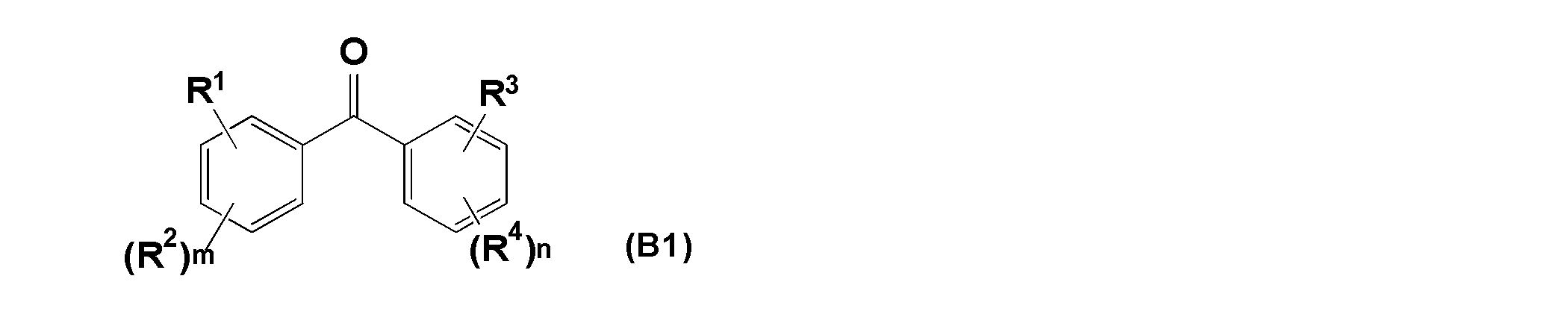
Examples of the benzophenone compound include a compound represented by the following formula (B1). The compound represented by the following formula (B1) is preferable because the protective film can efficiently absorb the energy of the laser beam and promote the thermal decomposition of the protective film.
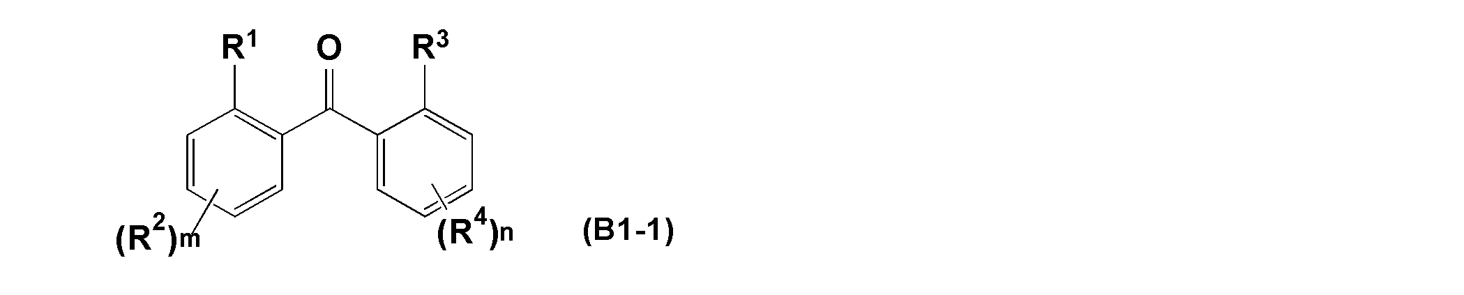

式(B1-1a)~式(B1-1e)で表される化合物において、R2が、-NR5R6で表される前述の基であって、R5及びR6が、それぞれ独立に炭素原子数1以上4以下のアルキル基であるのが好ましい。 Among the compounds represented by the formulas (B1-1a) to (B1-1e), the compound represented by the formula (B1-1a) is preferable.
In the compounds represented by the formulas (B1-1a) to (B1-1e), R 2 is the above-mentioned group represented by -NR 5 R 6 , and R 5 and R 6 are independent of each other. It is preferably an alkyl group having 1 or more and 4 or less carbon atoms.
これらの化合物は、入手の容易性や、塩基の存在下でも高い吸光係数を示すことから、好ましい。

These compounds are preferable because they are easily available and exhibit a high extinction coefficient even in the presence of a base.


これらの中でも、4-アミノ桂皮酸、3-アミノ桂皮酸、2-アミノ桂皮酸、及びフェルラ酸が好ましく、4-アミノ桂皮酸、及びフェルラ酸がより好ましく、4-アミノ桂皮酸が特に好ましい。 Specific examples of the cinnamic acid-based compound include 4-aminocinnamic acid, 3-aminocinnamic acid, 2-aminocinnamic acid, sinapinic acid (3,5-dimethoxy-4-hydroxycinnamic acid), ferulic acid, and caffeic acid. Can be mentioned.
Among these, 4-aminocinnamic acid, 3-aminocinnamic acid, 2-aminocinnamic acid, and ferulic acid are preferable, 4-aminocinnamic acid and ferulic acid are more preferable, and 4-aminocinnamic acid is particularly preferable.
保護膜に対してレーザー光を照射して加工溝を形成する際の開口不良や、保護膜の熱ダレによる加工溝の形状悪化等が生じにくいことから、保護膜形成剤における、水溶性樹脂(A)の質量と、吸光剤(B)の質量との総量に対する、吸光剤(B)の質量の比率は、1質量%以上50質量%以下が好ましく、5質量%以上40質量%以下がより好ましく、10質量%以上40質量%以下がさらに好ましい。
吸光剤(B)の含有量は、保護膜形成剤を塗布して形成される保護膜の吸光度が所望の値になるように設定できる。保護膜形成剤を塗布して形成される保護膜の吸光度は特に限定されないが、例えば、保護膜形成剤を塗布して形成される保護膜の波長355nmでの膜厚1μmあたりの吸光度が、0.3以上であることが好ましく、0.8以上であることがより好ましく、1.0以上であることがさらに好ましい。 The content of the light absorbing agent (B) in the protective film forming agent is not particularly limited as long as it does not impair the object of the present invention. The content of the light absorbing agent (B) in the protective film forming agent is preferably 0.1% by mass or more and 10% by mass or less. Since the protective film forming agent has excellent solubility of the light absorbing agent (B), the content of the light absorbing agent (B) can be increased.
A water-soluble resin in the protective film forming agent ( The ratio of the mass of the absorbent (B) to the total mass of the mass of A) and the mass of the absorbent (B) is preferably 1% by mass or more and 50% by mass or less, more preferably 5% by mass or more and 40% by mass or less. It is preferable, and more preferably 10% by mass or more and 40% by mass or less.
The content of the absorbent (B) can be set so that the absorbance of the protective film formed by applying the protective film forming agent becomes a desired value. The absorbance of the protective film formed by applying the protective film forming agent is not particularly limited. For example, the absorbance of the protective film formed by applying the protective film forming agent at a wavelength of 355 nm per 1 μm film thickness is 0. It is preferably .3 or more, more preferably 0.8 or more, and even more preferably 1.0 or more.
保護膜形成剤は、塩基性化合物(C)を必須成分として含む。塩基性化合物(C)を含むことにより、レーザー加工性に優れた保護膜を形成でき、且つ、吸光剤(B)の溶解性に優れた保護膜形成剤とすることができる。保護膜形成剤が吸光剤(B)の溶解性に優れるため、保護膜形成剤における吸光剤(B)の含有量を多くすることができる。また、形成される保護膜はレーザー加工性に優れているため、所望する溝を、保護膜中に容易に形成できる。 <Basic compound (C)>
The protective film forming agent contains the basic compound (C) as an essential component. By containing the basic compound (C), a protective film having excellent laser workability can be formed, and a protective film forming agent having excellent solubility of the light absorbing agent (B) can be obtained. Since the protective film-forming agent has excellent solubility of the light-absorbing agent (B), the content of the light-absorbing agent (B) in the protective film-forming agent can be increased. Further, since the protective film to be formed is excellent in laser workability, a desired groove can be easily formed in the protective film.
塩基性化合物(C)の具体例としては、水酸化ナトリウム、水酸化カリウム、炭酸ナトリウム、炭酸カリウム、ケイ酸ナトリウム、メタケイ酸ナトリウム、アンモニア;エチルアミン、n-プロピルアミン、モノエタノールアミン、ジエチルアミン、ジ-n-プロピルアミン、ジエタノールアミン、トリエチルアミン、メチルジエチルアミン、ジメチルエタノールアミン、トリエタノールアミン、テトラメチルアンモニウムヒドロキシド、テトラエチルアンモニウムヒドロキシド、イミダゾール、2-メチルイミダゾール、1,2-メチルイミダゾール、N-メチルイミダゾール、4-メチルイミダゾール、2-エチルイミダゾール、2-エチル-4-メチルイミダゾール、ピロール、ピペリジン、1,8-ジアザビシクロ[5,4,0]-7-ウンデセン、及び1,5-ジアザビシクロ[4,3,0]-5-ノナンが挙げられる。
なお、本明細書において、上記塩基性化合物(C)を、溶媒(S)に該当しない成分として定義する。 As the basic compound (C), either an inorganic compound or an organic compound can be used, and examples thereof include alkylamines, alkanolamines, imidazole compounds, and hydroxides of ammonia and alkali metals.
Specific examples of the basic compound (C) include sodium hydroxide, potassium hydroxide, sodium carbonate, potassium carbonate, sodium silicate, sodium metasilicate, and ammonia; ethylamine, n-propylamine, monoethanolamine, diethylamine, and di. -N-propylamine, diethanolamine, triethylamine, methyldiethylamine, dimethylethanolamine, triethanolamine, tetramethylammonium hydroxide, tetraethylammonium hydroxide, imidazole, 2-methylimidazole, 1,2-methylimidazole, N-methylimidazole , 4-Methylimidazole, 2-ethylimidazole, 2-ethyl-4-methylimidazole, pyrrole, piperidine, 1,8-diazabicyclo [5,4,0] -7-undecene, and 1,5-diazabicyclo [4, 3,0] -5-Nonan can be mentioned.
In this specification, the basic compound (C) is defined as a component that does not correspond to the solvent (S).
保護膜形成剤は、水溶性樹脂(A)、吸光剤(B)及び塩基性化合物(C)以外にも、本発明の目的を阻害しない限りにおいて、他の配合剤を含んでいてもよい。他の配合剤としては、例えば、防腐剤、及び界面活性剤等を用いることができる。 <Other additives>
The protective film forming agent may contain other compounding agents other than the water-soluble resin (A), the light absorbing agent (B) and the basic compound (C) as long as the object of the present invention is not impaired. As other compounding agents, for example, preservatives, surfactants and the like can be used.
保護膜形成剤は、水溶性樹脂(A)、吸光剤(B)や塩基性化合物(C)を溶解させるために、溶媒(S)を含む。溶媒(S)としては、水、有機溶剤、及び有機溶剤の水溶液のいずれも用いることができる。使用時の引火等の危険が少ないことや、コストの点等で、溶媒(S)としては、水、及び有機溶剤の水溶液が好ましく、水がより好ましい。 <Solvent (S)>
The protective film forming agent contains a solvent (S) in order to dissolve the water-soluble resin (A), the light absorbing agent (B) and the basic compound (C). As the solvent (S), any of water, an organic solvent, and an aqueous solution of an organic solvent can be used. As the solvent (S), water and an aqueous solution of an organic solvent are preferable, and water is more preferable, from the viewpoint of less risk of ignition during use and cost.
引火点をもたない保護膜形成剤は安全であり、例えば、非防爆環境下に置くことができる。具体的には、保護膜形成剤の保管、輸送、使用等の取扱いを非防爆環境下に行うことができる。例えば、保護膜形成剤の半導体工場への導入のみならず、保護膜の形成を非防爆環境下に行うことができる。従って、通常高価な防爆設備等の防爆環境が不要である点で、引火点をもたない保護膜形成剤は、産業上非常に有利である。 The solvent (S) is preferably selected so that the protective film forming agent does not have a flash point under 1 atm. Specifically, by adjusting the water content in the protective film forming agent, the flash point of the protective film and the presence or absence of the flash point are adjusted.
Protective film-forming agents that do not have a flash point are safe and can be placed, for example, in a non-explosion-proof environment. Specifically, the protective film forming agent can be stored, transported, used, etc. in a non-explosion-proof environment. For example, not only the protective film forming agent can be introduced into a semiconductor factory, but also the protective film can be formed in a non-explosion-proof environment. Therefore, a protective film forming agent having no flash point is industrially very advantageous in that an explosion-proof environment such as an explosion-proof facility, which is usually expensive, is not required.
本明細書においては、クリーブランド開放式で測定しても、引火点が測定できなかった場合を、引火点なしとする。 The flash point is obtained by measuring with a tag closed type when the liquid temperature is 80 ° C. or lower and by using the Cleveland open type when the liquid temperature exceeds 80 ° C. under 1 atm.
In the present specification, the case where the flash point cannot be measured even if the measurement is performed by the Cleveland open type is defined as no flash point.
アルキレングリコールとしては、エチレングリコール、及びプロピレングリコール等が挙げられる。アルキレングリコールモノアルキルエーテルとしては、エチレングリコールモノメチルエーテル、エチレングリコールモノエチルエーテル、プロピレングリコールモノメチルエーテル、及びプロピレングリコールモノエチルエーテル等が挙げられる。アルキレングリコールモノアルキルエーテルアセテートとしては、エチレングリコールモノメチルエーテルアセテート、エチレングリコールモノエチルエーテルアセテート、プロピレングリコールモノメチルエーテルアセテート、及びプロピレングリコールモノエチルエーテルアセテート等が挙げられる。
保護膜形成剤は、2種以上の有機溶剤を組み合わせて含んでいてもよい。 Examples of the organic solvent that can be contained in the protective film forming agent include methyl alcohol, ethyl alcohol, alkylene glycol, alkylene glycol monoalkyl ether, alkylene glycol monoalkyl ether acetate and the like.
Examples of the alkylene glycol include ethylene glycol and propylene glycol. Examples of the alkylene glycol monoalkyl ether include ethylene glycol monomethyl ether, ethylene glycol monoethyl ether, propylene glycol monomethyl ether, and propylene glycol monoethyl ether. Examples of the alkylene glycol monoalkyl ether acetate include ethylene glycol monomethyl ether acetate, ethylene glycol monoethyl ether acetate, propylene glycol monomethyl ether acetate, and propylene glycol monoethyl ether acetate.
The protective film forming agent may contain a combination of two or more kinds of organic solvents.
半導体チップの製造方法は、半導体ウエハーを加工して半導体チップを製造することを含む方法である。
より具体的には、半導体チップの製造方法は、
半導体ウエハー上に、前述の保護膜形成剤を塗布して保護膜を形成することと、
半導体ウエハー上における保護膜を含む1以上の層の所定の位置にレーザー光を照射し、半導体ウエハーの表面が露出し、且つ半導体チップの形状に応じたパターンの加工溝を形成することと、
を含む方法である。
典型的には、上記の半導体チップの製造方法は、半導体ウエハーにおけるストリートの位置を切断する切断工程を含む。
以下、保護膜を形成することについて「保護膜形成工程」とも記し、加工溝を形成することについて「加工溝形成工程」とも記し、半導体ウエハーにおけるストリートの位置を切断することについて「切断工程」とも記す。 ≪Manufacturing method of semiconductor chips≫
The method for manufacturing a semiconductor chip is a method including processing a semiconductor wafer to manufacture a semiconductor chip.
More specifically, the method for manufacturing a semiconductor chip is as follows.
To form a protective film by applying the above-mentioned protective film forming agent on a semiconductor wafer,
By irradiating a predetermined position of one or more layers including a protective film on a semiconductor wafer with laser light, the surface of the semiconductor wafer is exposed and a processing groove having a pattern corresponding to the shape of the semiconductor chip is formed.
It is a method including.
Typically, the semiconductor chip manufacturing method described above includes a cutting step of cutting a street position on a semiconductor wafer.
Hereinafter, forming a protective film is also referred to as a "protective film forming step", forming a machined groove is also referred to as a "working groove forming step", and cutting a street position on a semiconductor wafer is also referred to as a "cutting step". I will write it.
保護膜形成工程では、半導体ウエハー上に、前述の保護膜形成剤を塗布して保護膜が形成される。 <Protective film forming process>
In the protective film forming step, the protective film forming agent described above is applied onto the semiconductor wafer to form the protective film.
半導体ウエハーの加工面では、半導体チップに相当する複数の領域が、ストリートによって区画される。
加工後の水洗による保護膜の除去が容易であることや、後述する切断工程においてプラズマ照射を行う場合のプラズマ照射に対する保護膜の十分な耐久性の点で、保護膜の膜厚は、典型的には、1μm以上100μm以下が好ましく、10μm以上100μm以下がより好ましい。30μm以上100μm以下がさらに好ましい。
加工溝形成工程及び/又は切断工程においてレーザーを照射する場合、保護膜の膜厚は、0.1μm以上10μm以下が好ましい。
切断工程において、ブレードによる切断を行う場合、保護膜の膜厚は特に制限されない。ブレードによる切断を行う場合、加工後の水洗による保護膜の除去が容易であることから、保護膜の厚さは、例えば、0.1μm以上100μm以下が好ましい。 The shape of the processed surface of the semiconductor wafer is not particularly limited as long as the desired processing can be applied to the semiconductor wafer. Typically, the machined surface of a semiconductor wafer has a large number of irregularities. A recess is formed in the area corresponding to the street.
On the processed surface of the semiconductor wafer, a plurality of regions corresponding to semiconductor chips are partitioned by streets.
The film thickness of the protective film is typical in terms of easy removal of the protective film by washing with water after processing and sufficient durability of the protective film against plasma irradiation when plasma irradiation is performed in the cutting step described later. Is preferably 1 μm or more and 100 μm or less, and more preferably 10 μm or more and 100 μm or less. More preferably, it is 30 μm or more and 100 μm or less.
When the laser is irradiated in the processing groove forming step and / or the cutting step, the film thickness of the protective film is preferably 0.1 μm or more and 10 μm or less.
When cutting with a blade in the cutting step, the film thickness of the protective film is not particularly limited. When cutting with a blade, the thickness of the protective film is preferably 0.1 μm or more and 100 μm or less, for example, because the protective film can be easily removed by washing with water after processing.
ここで、半導体チップ22の、形状、及びサイズは特に限定されず、半導体チップ22の設計に応じて、適宜設定され得る。 FIG. 1 shows a perspective view of a semiconductor wafer to be processed. FIG. 2 shows an enlarged cross-sectional view of a main part of the semiconductor wafer shown in FIG. In the
Here, the shape and size of the
加工溝形成工程では、半導体ウエハー2上における保護膜24を含む1以上の層の所定の位置にレーザー光を照射し、半導体基板20の表面20aが露出し、且つ半導体チップ22の形状に応じたパターンの加工溝が形成される。 <Processing groove forming process>
In the processing groove forming step, laser light is irradiated to a predetermined position of one or more layers including the
レーザーは強度の点から波長100nm以上400nm以下である紫外線レーザーが好ましい。また、波長266nm、355nm等のYVO4レーザー、及びYAGレーザーが好ましい。 Specifically, the
From the viewpoint of intensity, the laser is preferably an ultraviolet laser having a wavelength of 100 nm or more and 400 nm or less. Further, a YVO4 laser having a wavelength of 266 nm and 355 nm and the like, and a YAG laser are preferable.
レーザー光の光源 :YVO4レーザー又はYAGレーザー
波長 :355nm
繰り返し周波数:50kHz以上100kHz以下
出力 :0.3W以上4.0W以下
加工送り速度 :1mm/秒以上800mm/秒以下 The laser light irradiation in the processing groove forming step is performed under the following processing conditions, for example. The diameter of the condensing spot is appropriately selected in consideration of the width of the
Laser light source: YVO4 laser or YAG laser Wavelength: 355 nm
Repeat frequency: 50 kHz or more and 100 kHz or less Output: 0.3 W or more and 4.0 W or less Processing feed rate: 1 mm / sec or more and 800 mm / sec or less
切断工程では、ストリート23の位置に対応する位置に加工溝25を備える半導体ウエハー2を切断する。好ましい方法としては、保護膜24と加工溝25とを備える半導体ウエハー2にレーザー又はプラズマを照射することにより半導体ウエハー2を切断する方法や、保護膜24を備える半導体ウエハー2、又は保護膜24が剥離された半導体ウエハー2をブレードにより切断する方法が挙げられる。レーザーを照射する場合、半導体ウエハー2を切断すべく、加工溝25に対してレーザーが照射される。プラズマを照射する場合、加工溝25の表面にプラズマが暴露されるように、半導体ウエハー2の保護膜を備える面の一部又は全面にプラズマが照射される。ブレードにより切断を行う場合、切断箇所に純水を供給しながら、加工溝25の位置に沿って、ブレードにより半導体ウエハー2が切断される。
以下、好ましい切断方法であるプラズマ照射による切断方法について説明する。 <Cutting process>
In the cutting step, the
Hereinafter, a cutting method by plasma irradiation, which is a preferable cutting method, will be described.
具体的には、保護膜24で被覆された半導体ウエハー2において、上記の通り、加工溝25を形成した後、保護膜24と、加工溝25から露出する半導体基板20の表面20aとに対して、プラズマ照射を行うことにより、半導体ウエハー2が、半導体チップ22の形状に従って切断され、半導体ウエハー2が半導体チップ22に分割される。 As shown in FIG. 7, the
Specifically, in the
プラズマ照射においてプラズマを生成させるために用いられるガスとしては、半導体ウエハー2の材質に応じて適宜選択される。典型的には、プラズマの生成にはSF6ガスが使用される。
また、所謂BOSCHプロセスに従い、C4F6又はC4F8ガス等の供給による側壁保護と、プラズマ照射による半導体ウエハー2のエッチングとを交互に行うことにより、半導体ウエハー2の切断を行ってもよい。BOSCHプロセスによれば、高アスペクト比でのエッチングが可能であり、半導体ウエハー2が厚い場合でも、半導体ウエハー2の切断が容易である。 The plasma irradiation conditions are not particularly limited as long as the
The gas used to generate plasma in plasma irradiation is appropriately selected depending on the material of the
Further, even if the
実施例1~15、及び比較例1~12では、水溶性樹脂(A)として、ヒドロキシプロピルセルロース(A1)、ポリビニルピロリドン(A2)を用いた。
また、吸光剤(B)として、下記式で表されるB1~B4を用いた。

また、溶媒(S)として、水(S1)、プロピレングリコールモノメチルエーテル(PGME)(S2)を用いた。 [Examples 1 to 15 and Comparative Examples 1 to 12]
In Examples 1 to 15 and Comparative Examples 1 to 12, hydroxypropyl cellulose (A1) and polyvinylpyrrolidone (A2) were used as the water-soluble resin (A).
Further, as the light absorbing agent (B), B1 to B4 represented by the following formulas were used.
Further, as the solvent (S), water (S1) and propylene glycol monomethyl ether (PGME) (S2) were used.
それぞれ表1~3に記載の種類及び量の、水溶性樹脂(A)と、吸光剤(B)と、塩基性化合物(C)と、溶媒(S)とを、容器に投入し、8時間撹拌して、各実施例及び比較例の保護膜形成剤を得た。なお、表1~3の配合の数値(量)の単位は、質量%である。 (Manufacturing of protective film forming agent)
The water-soluble resin (A), the light absorbing agent (B), the basic compound (C), and the solvent (S) of the types and amounts shown in Tables 1 to 3, respectively, were put into a container for 8 hours. Stirring was performed to obtain protective film forming agents of each Example and Comparative Example. The unit of the numerical value (amount) of the formulation in Tables 1 to 3 is mass%.
得られた保護膜形成剤を目視で観察して、後述する評価基準に従い評価した。結果を表1~3に記す。
<吸光剤の溶解性評価基準>
○:吸光剤の溶け残りが無かった。
×:吸光剤の溶け残りがあった。 (Evaluation of solubility of absorbent)
The obtained protective film forming agent was visually observed and evaluated according to the evaluation criteria described later. The results are shown in Tables 1-3.
<Criteria for evaluating solubility of absorbent>
◯: There was no undissolved residue of the absorbent.
X: There was undissolved residue of the light absorber.
得られた保護膜形成剤を用いて、ガラス基板上にスピンコート法(スピンコート条件:2000rpm、120秒)により保護膜を形成した。
形成された保護膜について、分光光度計(MCPD-3000(大塚電子製))を用いて透過率の測定を行い、透過率の測定結果から波長355nmでの膜厚1μmあたりの吸光度を測定した。測定結果を表1~3に記す。なお、吸光剤の溶け残りが観察された保護膜形成剤については、吸光度を測定しなかった。 (Measurement of absorbance of protective film (coating film))
Using the obtained protective film forming agent, a protective film was formed on a glass substrate by a spin coating method (spin coating conditions: 2000 rpm, 120 seconds).
The transmittance of the formed protective film was measured using a spectrophotometer (MCPD-3000 (manufactured by Otsuka Electronics Co., Ltd.)), and the absorbance per 1 μm film thickness at a wavelength of 355 nm was measured from the measurement result of the transmittance. The measurement results are shown in Tables 1 to 3. The absorbance of the protective film-forming agent in which the undissolved residue of the absorbent was observed was not measured.
得られた保護膜形成剤を、シリコン基板上に2μmの膜厚になるようにスピンコート法により塗布して、保護膜を形成した。
保護膜を備えるシリコン基板の保護膜側の面に対して、以下の条件で直線状にレーザー照射を行った。その後、保護膜を除去し、レーザー照射された箇所(加工部)及びその近傍を光学顕微鏡により観察して、後述する評価基準に従い評価した。レーザー加工性が悪いと、保護膜の分解除去がし難く、保護膜が分解除去されずに、膜の状態で基板から剥がれ、剥がれた部分に基板のデブリが付着する。そのため、保護膜を除去後の加工部及びその近傍を観察することで、レーザー加工性を評価することができる。 (Evaluation of laser workability)
The obtained protective film forming agent was applied onto a silicon substrate by a spin coating method so as to have a film thickness of 2 μm to form a protective film.
The surface of the silicon substrate provided with the protective film on the protective film side was linearly irradiated with a laser under the following conditions. After that, the protective film was removed, and the laser-irradiated portion (processed portion) and its vicinity were observed with an optical microscope and evaluated according to the evaluation criteria described later. If the laser workability is poor, it is difficult to decompose and remove the protective film, and the protective film is not decomposed and removed, but is peeled off from the substrate in the state of the film, and debris on the substrate adheres to the peeled portion. Therefore, the laser workability can be evaluated by observing the processed portion and its vicinity after removing the protective film.
波長:355nm
周波数:100kHz
出力:0.8W
デフォーカス:-0.0mm
送り速度:100mm/s
Pass:1 <Laser irradiation conditions>
Wavelength: 355 nm
Frequency: 100kHz
Output: 0.8W
Defocus: -0.0mm
Feed rate: 100 mm / s
Pass: 1
〇:加工部の外側にデブリの付着が観察されなかった。
×:加工部の外側にデブリの付着が観察された。 <Cross-sectional shape evaluation criteria>
〇: No debris adhesion was observed on the outside of the processed part.
X: Adhesion of debris was observed on the outside of the processed portion.


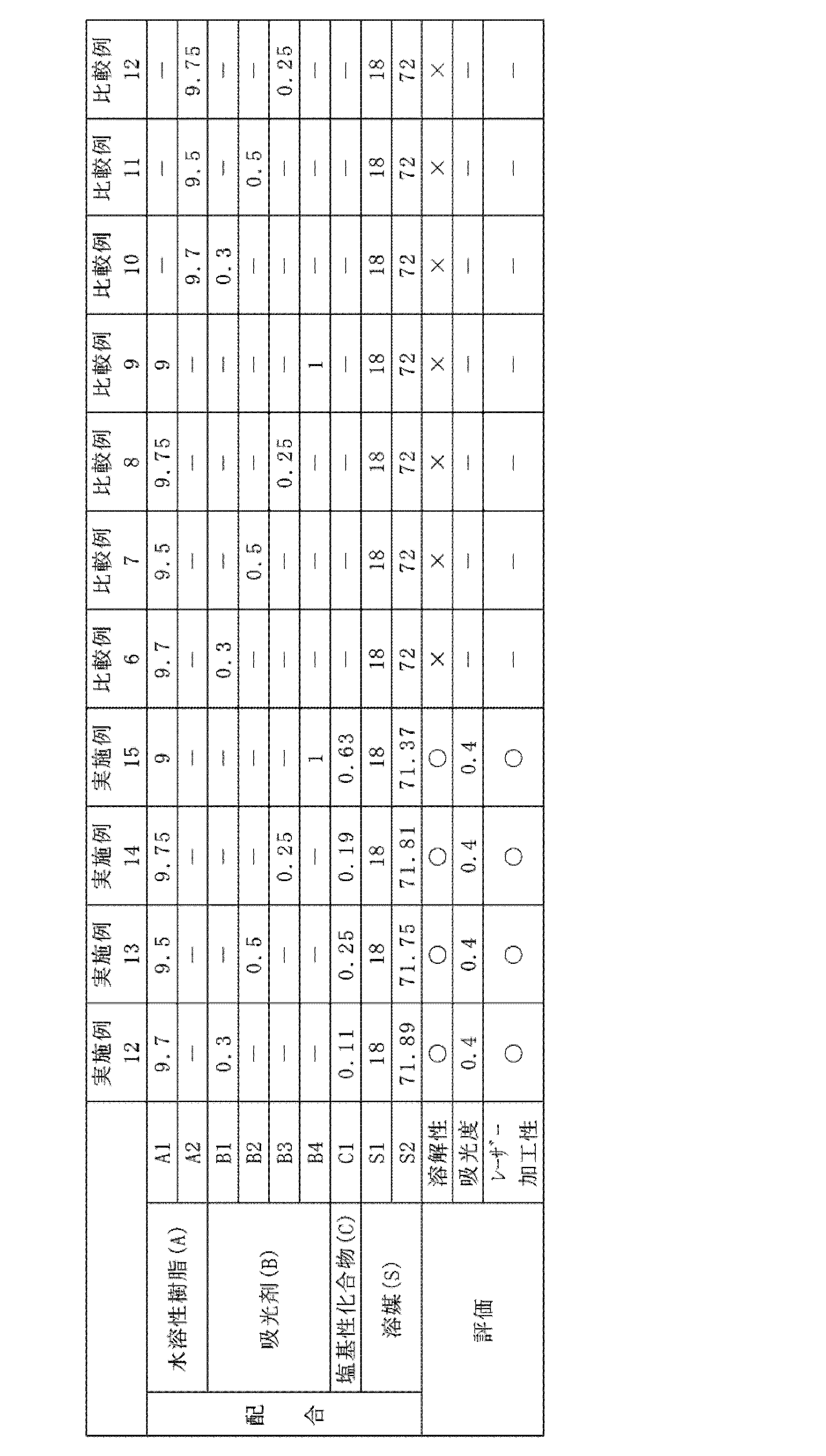
他方、表1~3から、塩基性化合物(C)を含まない比較例1~12の保護膜形成剤は、吸光剤の溶解性や保護膜のレーザー加工性が悪いことが分かる。 From Tables 1 to 3, the protective film-forming agents of Examples 1 to 14 containing the water-soluble resin (A), the light-absorbing agent (B), the basic compound (C), and the solvent (S) are the light-absorbing agents. It can be seen that the solubility of the resin is excellent. Further, it can be seen that the protective film formed by using the protective film forming agent of Examples 1 to 14 has high absorbance and is excellent in laser processability.
On the other hand, from Tables 1 to 3, it can be seen that the protective film forming agents of Comparative Examples 1 to 12 containing no basic compound (C) have poor solubility of the light absorbing agent and poor laser processability of the protective film.
20 :基板
21 :積層体
22 :半導体チップ
23 :ストリート
24 :保護膜
25 :レーザー加工溝
26 :切削溝
3 :スピンコーター
5 :環状のフレーム
6 :保護テープ
7 :レーザー加工装置
71 :レーザー加工装置のチャックテーブル
72 :レーザー光線照射手段 2: Semiconductor wafer 20: Substrate 21: Laminated body 22: Semiconductor chip 23: Street 24: Protective film 25: Laser processing groove 26: Cutting groove 3: Spin coater 5: Circular frame 6: Protective tape 7: Laser processing device 71 : Chuck table of laser processing equipment 72: Laser beam irradiation means
Claims (7)
- 半導体ウエハーのダイシングにおいて、半導体ウエハーの表面に保護膜を形成するために用いられる保護膜形成剤であって、
水溶性樹脂(A)と、吸光剤(B)と、塩基性化合物(C)と、溶媒(S)とを含む、保護膜形成剤。 A protective film forming agent used for forming a protective film on the surface of a semiconductor wafer in dicing of a semiconductor wafer.
A protective film-forming agent containing a water-soluble resin (A), an absorptive agent (B), a basic compound (C), and a solvent (S). - 前記塩基性化合物(C)が、アルキルアミン、アルカノールアミン、イミダゾール化合物、アンモニア及びアルカリ金属の水酸化物から選択される少なくとも一種を含む、請求項1に記載の保護膜形成剤。 The protective film-forming agent according to claim 1, wherein the basic compound (C) contains at least one selected from alkylamines, alkanolamines, imidazole compounds, ammonia and hydroxides of alkali metals.
- 前記吸光剤(B)が、ベンゾフェノン系化合物、桂皮酸系化合物、アントラキノン系化合物、ナフタレン系化合物及びビフェニル系化合物から選択される少なくとも一種を含む、請求項1又は2に記載の保護膜形成剤。 The protective film forming agent according to claim 1 or 2, wherein the light absorbing agent (B) contains at least one selected from a benzophenone compound, a cinnamic acid compound, an anthraquinone compound, a naphthalene compound and a biphenyl compound.
- 前記吸光剤(B)の含有量が、0.1質量%以上10質量%以下である、請求項1~3のいずれか1項に記載の保護膜形成剤。 The protective film forming agent according to any one of claims 1 to 3, wherein the content of the light absorbing agent (B) is 0.1% by mass or more and 10% by mass or less.
- 前記溶媒(S)が、水を含む、請求項1~4のいずれか1項に記載の保護膜形成剤。 The protective film forming agent according to any one of claims 1 to 4, wherein the solvent (S) contains water.
- 前記溶媒(S)中の有機溶媒の含有量が、20質量%以下である、請求項1~5のいずれか1項に記載の保護膜形成剤。 The protective film forming agent according to any one of claims 1 to 5, wherein the content of the organic solvent in the solvent (S) is 20% by mass or less.
- 半導体ウエハーを加工する、半導体チップの製造方法であって、
前記半導体ウエハー上に、請求項1~6のいずれか1項に記載の前記保護膜形成剤を塗布して保護膜を形成することと、
前記半導体ウエハー上における前記保護膜を含む1以上の層の所定の位置にレーザー光を照射し、前記半導体ウエハーの表面が露出し、且つ半導体チップの形状に応じたパターンの加工溝を形成することと、
を含む、半導体チップの製造方法。 A method for manufacturing semiconductor chips that processes semiconductor wafers.
The protective film forming agent according to any one of claims 1 to 6 is applied onto the semiconductor wafer to form a protective film.
Irradiating a predetermined position of one or more layers including the protective film on the semiconductor wafer with laser light to expose the surface of the semiconductor wafer and forming a processing groove having a pattern according to the shape of the semiconductor chip. When,
A method for manufacturing a semiconductor chip, including.
Priority Applications (5)
| Application Number | Priority Date | Filing Date | Title |
|---|---|---|---|
| US17/756,790 US20220392806A1 (en) | 2019-12-24 | 2020-11-26 | Protective film forming agent, and method for producing semiconductor chip |
| JP2021567085A JPWO2021131472A1 (en) | 2019-12-24 | 2020-11-26 | |
| EP20906549.9A EP4060717A4 (en) | 2019-12-24 | 2020-11-26 | Protective film formation agent, and method for manufacturing semiconductor chip |
| CN202080087446.6A CN114830301A (en) | 2019-12-24 | 2020-11-26 | Protective film forming agent and method for manufacturing semiconductor chip |
| KR1020227023114A KR20220119634A (en) | 2019-12-24 | 2020-11-26 | A protective film forming agent and a method for manufacturing a semiconductor chip |
Applications Claiming Priority (2)
| Application Number | Priority Date | Filing Date | Title |
|---|---|---|---|
| JP2019233126 | 2019-12-24 | ||
| JP2019-233126 | 2019-12-24 |
Publications (1)
| Publication Number | Publication Date |
|---|---|
| WO2021131472A1 true WO2021131472A1 (en) | 2021-07-01 |
Family
ID=76574361
Family Applications (1)
| Application Number | Title | Priority Date | Filing Date |
|---|---|---|---|
| PCT/JP2020/043941 WO2021131472A1 (en) | 2019-12-24 | 2020-11-26 | Protective film formation agent, and method for manufacturing semiconductor chip |
Country Status (7)
| Country | Link |
|---|---|
| US (1) | US20220392806A1 (en) |
| EP (1) | EP4060717A4 (en) |
| JP (1) | JPWO2021131472A1 (en) |
| KR (1) | KR20220119634A (en) |
| CN (1) | CN114830301A (en) |
| TW (1) | TW202132484A (en) |
| WO (1) | WO2021131472A1 (en) |
Families Citing this family (2)
| Publication number | Priority date | Publication date | Assignee | Title |
|---|---|---|---|---|
| WO2020100403A1 (en) * | 2018-11-15 | 2020-05-22 | 東京応化工業株式会社 | Protective film forming agent for plasma dicing and method for manufacturing semiconductor chip |
| JP2022085738A (en) * | 2020-11-27 | 2022-06-08 | パナソニックIpマネジメント株式会社 | Chip manufacturing method |
Citations (10)
| Publication number | Priority date | Publication date | Assignee | Title |
|---|---|---|---|---|
| JP2006140311A (en) * | 2004-11-12 | 2006-06-01 | Tokyo Ohka Kogyo Co Ltd | Protective film agent used for laser dicing and method of processing wafer using the same |
| JP2016066768A (en) * | 2014-09-26 | 2016-04-28 | 富士フイルム株式会社 | Protection film composition, method for manufacturing semiconductor device, and laser dicing method |
| WO2018217481A1 (en) * | 2017-05-26 | 2018-11-29 | Applied Materials, Inc. | Light-absorbing mask for hybrid laser scribing and plasma etch wafer singulation process |
| JP2019012807A (en) * | 2017-07-03 | 2019-01-24 | 日化精工株式会社 | Protective film agent for laser processing |
| JP2019518328A (en) * | 2016-05-13 | 2019-06-27 | アプライド マテリアルズ インコーポレイテッドApplied Materials,Incorporated | Etching mask for hybrid wafer singulation process by laser scribing / plasma etching |
| JP2019212765A (en) * | 2018-06-05 | 2019-12-12 | パナソニックIpマネジメント株式会社 | Method for manufacturing element chip |
| JP2019212764A (en) * | 2018-06-05 | 2019-12-12 | パナソニックIpマネジメント株式会社 | Method for manufacturing element chip |
| JP2020066665A (en) * | 2018-10-23 | 2020-04-30 | 日本酢ビ・ポバール株式会社 | Protective film-forming composition |
| JP2020066666A (en) * | 2018-10-23 | 2020-04-30 | 日本酢ビ・ポバール株式会社 | Protective film-forming composition |
| JP2020066667A (en) * | 2018-10-23 | 2020-04-30 | 日本酢ビ・ポバール株式会社 | Protective film-forming composition |
Family Cites Families (2)
| Publication number | Priority date | Publication date | Assignee | Title |
|---|---|---|---|---|
| US8703581B2 (en) | 2011-06-15 | 2014-04-22 | Applied Materials, Inc. | Water soluble mask for substrate dicing by laser and plasma etch |
| CN105489472B (en) * | 2014-09-16 | 2019-03-15 | 长春石油化学股份有限公司 | Preceding cutting protection liquid and the wafer processing method that liquid is protected using this |
-
2020
- 2020-11-26 CN CN202080087446.6A patent/CN114830301A/en active Pending
- 2020-11-26 JP JP2021567085A patent/JPWO2021131472A1/ja active Pending
- 2020-11-26 US US17/756,790 patent/US20220392806A1/en active Pending
- 2020-11-26 EP EP20906549.9A patent/EP4060717A4/en active Pending
- 2020-11-26 KR KR1020227023114A patent/KR20220119634A/en unknown
- 2020-11-26 WO PCT/JP2020/043941 patent/WO2021131472A1/en unknown
- 2020-12-09 TW TW109143378A patent/TW202132484A/en unknown
Patent Citations (10)
| Publication number | Priority date | Publication date | Assignee | Title |
|---|---|---|---|---|
| JP2006140311A (en) * | 2004-11-12 | 2006-06-01 | Tokyo Ohka Kogyo Co Ltd | Protective film agent used for laser dicing and method of processing wafer using the same |
| JP2016066768A (en) * | 2014-09-26 | 2016-04-28 | 富士フイルム株式会社 | Protection film composition, method for manufacturing semiconductor device, and laser dicing method |
| JP2019518328A (en) * | 2016-05-13 | 2019-06-27 | アプライド マテリアルズ インコーポレイテッドApplied Materials,Incorporated | Etching mask for hybrid wafer singulation process by laser scribing / plasma etching |
| WO2018217481A1 (en) * | 2017-05-26 | 2018-11-29 | Applied Materials, Inc. | Light-absorbing mask for hybrid laser scribing and plasma etch wafer singulation process |
| JP2019012807A (en) * | 2017-07-03 | 2019-01-24 | 日化精工株式会社 | Protective film agent for laser processing |
| JP2019212765A (en) * | 2018-06-05 | 2019-12-12 | パナソニックIpマネジメント株式会社 | Method for manufacturing element chip |
| JP2019212764A (en) * | 2018-06-05 | 2019-12-12 | パナソニックIpマネジメント株式会社 | Method for manufacturing element chip |
| JP2020066665A (en) * | 2018-10-23 | 2020-04-30 | 日本酢ビ・ポバール株式会社 | Protective film-forming composition |
| JP2020066666A (en) * | 2018-10-23 | 2020-04-30 | 日本酢ビ・ポバール株式会社 | Protective film-forming composition |
| JP2020066667A (en) * | 2018-10-23 | 2020-04-30 | 日本酢ビ・ポバール株式会社 | Protective film-forming composition |
Non-Patent Citations (1)
| Title |
|---|
| See also references of EP4060717A4 |
Also Published As
| Publication number | Publication date |
|---|---|
| TW202132484A (en) | 2021-09-01 |
| JPWO2021131472A1 (en) | 2021-07-01 |
| EP4060717A1 (en) | 2022-09-21 |
| CN114830301A (en) | 2022-07-29 |
| EP4060717A4 (en) | 2023-12-13 |
| KR20220119634A (en) | 2022-08-30 |
| US20220392806A1 (en) | 2022-12-08 |
Similar Documents
| Publication | Publication Date | Title |
|---|---|---|
| JP7412915B2 (en) | Protective film forming agent and semiconductor chip manufacturing method | |
| US9090783B2 (en) | Protective film agent for laser dicing and wafer processing method using the protective film agent | |
| JP7017648B2 (en) | Protective film forming agent for plasma dicing and method for manufacturing semiconductor chips | |
| WO2021131472A1 (en) | Protective film formation agent, and method for manufacturing semiconductor chip | |
| TWI638870B (en) | Solution for forming protective layer used in picosecond laser process and method for manufacturing thereof | |
| WO2022153858A1 (en) | Protective film formation agent, and production method for semiconductor chip | |
| KR20190004206A (en) | Protective film material for laser processing | |
| KR20180111677A (en) | Protective film agent for dicing | |
| TW202124611A (en) | Protective film forming agent, method for producing semiconductor chip, and method for producing (meth)acrylic resin | |
| JP2023046873A (en) | Formation method for protective film, manufacturing method of semiconductor chip and preparation method for coating liquid | |
| JP2022125002A (en) | Method for producing semiconductor chip and protective film forming agent | |
| KR20220117146A (en) | Method for producing semiconductor chip and protective film forming agent | |
| WO2024034345A1 (en) | Protective film formation agent, and method for manufacturing semiconductor chip | |
| KR20170059588A (en) | Protective solution for laser processing |
Legal Events
| Date | Code | Title | Description |
|---|---|---|---|
| 121 | Ep: the epo has been informed by wipo that ep was designated in this application |
Ref document number: 20906549 Country of ref document: EP Kind code of ref document: A1 |
|
| ENP | Entry into the national phase |
Ref document number: 2021567085 Country of ref document: JP Kind code of ref document: A |
|
| ENP | Entry into the national phase |
Ref document number: 2020906549 Country of ref document: EP Effective date: 20220617 |
|
| ENP | Entry into the national phase |
Ref document number: 20227023114 Country of ref document: KR Kind code of ref document: A |
|
| NENP | Non-entry into the national phase |
Ref country code: DE |