WO2021112070A1 - Wafer processing temporary adhesive, wafer laminate, thin wafer manufacturing method - Google Patents
Wafer processing temporary adhesive, wafer laminate, thin wafer manufacturing method Download PDFInfo
- Publication number
- WO2021112070A1 WO2021112070A1 PCT/JP2020/044638 JP2020044638W WO2021112070A1 WO 2021112070 A1 WO2021112070 A1 WO 2021112070A1 JP 2020044638 W JP2020044638 W JP 2020044638W WO 2021112070 A1 WO2021112070 A1 WO 2021112070A1
- Authority
- WO
- WIPO (PCT)
- Prior art keywords
- wafer
- mass
- temporary adhesive
- parts
- group
- Prior art date
Links
- 239000000853 adhesive Substances 0.000 title claims abstract description 37
- 230000001070 adhesive effect Effects 0.000 title claims abstract description 37
- 238000012545 processing Methods 0.000 title claims abstract description 36
- 238000004519 manufacturing process Methods 0.000 title claims abstract description 14
- 229920001296 polysiloxane Polymers 0.000 claims abstract description 60
- 229920002050 silicone resin Polymers 0.000 claims abstract description 59
- 229920001187 thermosetting polymer Polymers 0.000 claims abstract description 47
- 239000011342 resin composition Substances 0.000 claims abstract description 33
- YXFVVABEGXRONW-UHFFFAOYSA-N Toluene Chemical compound CC1=CC=CC=C1 YXFVVABEGXRONW-UHFFFAOYSA-N 0.000 claims description 99
- 238000000034 method Methods 0.000 claims description 56
- 239000012790 adhesive layer Substances 0.000 claims description 47
- 239000000758 substrate Substances 0.000 claims description 28
- 125000003342 alkenyl group Chemical group 0.000 claims description 24
- 238000000227 grinding Methods 0.000 claims description 21
- XUIMIQQOPSSXEZ-UHFFFAOYSA-N Silicon Chemical group [Si] XUIMIQQOPSSXEZ-UHFFFAOYSA-N 0.000 claims description 20
- 238000012360 testing method Methods 0.000 claims description 17
- 229910052710 silicon Inorganic materials 0.000 claims description 16
- 238000006459 hydrosilylation reaction Methods 0.000 claims description 15
- 229920006136 organohydrogenpolysiloxane Polymers 0.000 claims description 15
- 239000010703 silicon Substances 0.000 claims description 15
- 239000007809 chemical reaction catalyst Substances 0.000 claims description 13
- 229910052751 metal Inorganic materials 0.000 claims description 11
- 239000002184 metal Substances 0.000 claims description 11
- 238000003860 storage Methods 0.000 claims description 11
- 125000004435 hydrogen atom Chemical group [H]* 0.000 claims description 6
- 239000003795 chemical substances by application Substances 0.000 claims description 5
- 238000005498 polishing Methods 0.000 claims description 3
- 235000012431 wafers Nutrition 0.000 description 151
- -1 siloxane unit Chemical group 0.000 description 52
- 238000002360 preparation method Methods 0.000 description 19
- 239000000203 mixture Substances 0.000 description 17
- 238000004140 cleaning Methods 0.000 description 16
- 239000004205 dimethyl polysiloxane Substances 0.000 description 16
- 235000013870 dimethyl polysiloxane Nutrition 0.000 description 16
- 229920000435 poly(dimethylsiloxane) Polymers 0.000 description 16
- 229920005989 resin Polymers 0.000 description 16
- 239000011347 resin Substances 0.000 description 16
- 125000000391 vinyl group Chemical group [H]C([*])=C([H])[H] 0.000 description 14
- 239000011521 glass Substances 0.000 description 12
- 150000002430 hydrocarbons Chemical class 0.000 description 12
- 239000002904 solvent Substances 0.000 description 12
- 239000010410 layer Substances 0.000 description 11
- 230000005856 abnormality Effects 0.000 description 10
- 230000015572 biosynthetic process Effects 0.000 description 10
- QYLFHLNFIHBCPR-UHFFFAOYSA-N 1-ethynylcyclohexan-1-ol Chemical compound C#CC1(O)CCCCC1 QYLFHLNFIHBCPR-UHFFFAOYSA-N 0.000 description 9
- 238000005229 chemical vapour deposition Methods 0.000 description 9
- 230000000052 comparative effect Effects 0.000 description 9
- 239000004065 semiconductor Substances 0.000 description 9
- 239000012528 membrane Substances 0.000 description 7
- BASFCYQUMIYNBI-UHFFFAOYSA-N platinum Chemical group [Pt] BASFCYQUMIYNBI-UHFFFAOYSA-N 0.000 description 7
- KFZMGEQAYNKOFK-UHFFFAOYSA-N Isopropanol Chemical compound CC(C)O KFZMGEQAYNKOFK-UHFFFAOYSA-N 0.000 description 6
- 239000002253 acid Substances 0.000 description 6
- 239000007788 liquid Substances 0.000 description 6
- VLKZOEOYAKHREP-UHFFFAOYSA-N n-Hexane Chemical compound CCCCCC VLKZOEOYAKHREP-UHFFFAOYSA-N 0.000 description 6
- 229910004283 SiO 4 Inorganic materials 0.000 description 5
- VYPSYNLAJGMNEJ-UHFFFAOYSA-N Silicium dioxide Chemical compound O=[Si]=O VYPSYNLAJGMNEJ-UHFFFAOYSA-N 0.000 description 5
- 125000004432 carbon atom Chemical group C* 0.000 description 5
- 230000002950 deficient Effects 0.000 description 5
- 238000002156 mixing Methods 0.000 description 5
- 125000001997 phenyl group Chemical group [H]C1=C([H])C([H])=C(*)C([H])=C1[H] 0.000 description 5
- OFBQJSOFQDEBGM-UHFFFAOYSA-N Pentane Chemical compound CCCCC OFBQJSOFQDEBGM-UHFFFAOYSA-N 0.000 description 4
- 229910004298 SiO 2 Inorganic materials 0.000 description 4
- 238000006243 chemical reaction Methods 0.000 description 4
- 229920001577 copolymer Polymers 0.000 description 4
- DIOQZVSQGTUSAI-UHFFFAOYSA-N decane Chemical compound CCCCCCCCCC DIOQZVSQGTUSAI-UHFFFAOYSA-N 0.000 description 4
- 229920005645 diorganopolysiloxane polymer Polymers 0.000 description 4
- XMGQYMWWDOXHJM-UHFFFAOYSA-N limonene Chemical compound CC(=C)C1CCC(C)=CC1 XMGQYMWWDOXHJM-UHFFFAOYSA-N 0.000 description 4
- 125000002496 methyl group Chemical group [H]C([H])([H])* 0.000 description 4
- 230000001681 protective effect Effects 0.000 description 4
- 239000000126 substance Substances 0.000 description 4
- QTBSBXVTEAMEQO-UHFFFAOYSA-N Acetic acid Chemical compound CC(O)=O QTBSBXVTEAMEQO-UHFFFAOYSA-N 0.000 description 3
- MUBZPKHOEPUJKR-UHFFFAOYSA-N Oxalic acid Chemical compound OC(=O)C(O)=O MUBZPKHOEPUJKR-UHFFFAOYSA-N 0.000 description 3
- KDLHZDBZIXYQEI-UHFFFAOYSA-N Palladium Chemical compound [Pd] KDLHZDBZIXYQEI-UHFFFAOYSA-N 0.000 description 3
- ZMANZCXQSJIPKH-UHFFFAOYSA-N Triethylamine Chemical compound CCN(CC)CC ZMANZCXQSJIPKH-UHFFFAOYSA-N 0.000 description 3
- 150000007513 acids Chemical class 0.000 description 3
- 125000001931 aliphatic group Chemical group 0.000 description 3
- 125000000217 alkyl group Chemical group 0.000 description 3
- 125000003118 aryl group Chemical group 0.000 description 3
- 239000003054 catalyst Substances 0.000 description 3
- 239000011248 coating agent Substances 0.000 description 3
- 238000000576 coating method Methods 0.000 description 3
- 150000001875 compounds Chemical class 0.000 description 3
- 238000005336 cracking Methods 0.000 description 3
- 238000010438 heat treatment Methods 0.000 description 3
- 238000005304 joining Methods 0.000 description 3
- 239000000463 material Substances 0.000 description 3
- 150000003058 platinum compounds Chemical class 0.000 description 3
- 229920000642 polymer Polymers 0.000 description 3
- 238000004528 spin coating Methods 0.000 description 3
- 229930195735 unsaturated hydrocarbon Natural products 0.000 description 3
- 229920002554 vinyl polymer Polymers 0.000 description 3
- HZAXFHJVJLSVMW-UHFFFAOYSA-N 2-Aminoethan-1-ol Chemical compound NCCO HZAXFHJVJLSVMW-UHFFFAOYSA-N 0.000 description 2
- CEBKHWWANWSNTI-UHFFFAOYSA-N 2-methylbut-3-yn-2-ol Chemical compound CC(C)(O)C#C CEBKHWWANWSNTI-UHFFFAOYSA-N 0.000 description 2
- GTJOHISYCKPIMT-UHFFFAOYSA-N 2-methylundecane Chemical compound CCCCCCCCCC(C)C GTJOHISYCKPIMT-UHFFFAOYSA-N 0.000 description 2
- QGZKDVFQNNGYKY-UHFFFAOYSA-N Ammonia Chemical compound N QGZKDVFQNNGYKY-UHFFFAOYSA-N 0.000 description 2
- XDTMQSROBMDMFD-UHFFFAOYSA-N Cyclohexane Chemical compound C1CCCCC1 XDTMQSROBMDMFD-UHFFFAOYSA-N 0.000 description 2
- LFQSCWFLJHTTHZ-UHFFFAOYSA-N Ethanol Chemical compound CCO LFQSCWFLJHTTHZ-UHFFFAOYSA-N 0.000 description 2
- SGVYKUFIHHTIFL-UHFFFAOYSA-N Isobutylhexyl Natural products CCCCCCCC(C)C SGVYKUFIHHTIFL-UHFFFAOYSA-N 0.000 description 2
- BOTDANWDWHJENH-UHFFFAOYSA-N Tetraethyl orthosilicate Chemical compound CCO[Si](OCC)(OCC)OCC BOTDANWDWHJENH-UHFFFAOYSA-N 0.000 description 2
- 229910052782 aluminium Inorganic materials 0.000 description 2
- 125000000484 butyl group Chemical group [H]C([*])([H])C([H])([H])C([H])([H])C([H])([H])[H] 0.000 description 2
- 238000001816 cooling Methods 0.000 description 2
- 125000004122 cyclic group Chemical group 0.000 description 2
- 125000000753 cycloalkyl group Chemical group 0.000 description 2
- 125000000113 cyclohexyl group Chemical group [H]C1([H])C([H])([H])C([H])([H])C([H])(*)C([H])([H])C1([H])[H] 0.000 description 2
- 239000010432 diamond Substances 0.000 description 2
- 229910003460 diamond Inorganic materials 0.000 description 2
- 125000000118 dimethyl group Chemical group [H]C([H])([H])* 0.000 description 2
- 238000005516 engineering process Methods 0.000 description 2
- 125000003700 epoxy group Chemical group 0.000 description 2
- 238000005530 etching Methods 0.000 description 2
- 125000001495 ethyl group Chemical group [H]C([H])([H])C([H])([H])* 0.000 description 2
- 125000005843 halogen group Chemical group 0.000 description 2
- VKPSKYDESGTTFR-UHFFFAOYSA-N isododecane Natural products CC(C)(C)CC(C)CC(C)(C)C VKPSKYDESGTTFR-UHFFFAOYSA-N 0.000 description 2
- 229940087305 limonene Drugs 0.000 description 2
- 235000001510 limonene Nutrition 0.000 description 2
- BKIMMITUMNQMOS-UHFFFAOYSA-N nonane Chemical compound CCCCCCCCC BKIMMITUMNQMOS-UHFFFAOYSA-N 0.000 description 2
- 125000000962 organic group Chemical group 0.000 description 2
- CFJYNSNXFXLKNS-UHFFFAOYSA-N p-menthane Chemical compound CC(C)C1CCC(C)CC1 CFJYNSNXFXLKNS-UHFFFAOYSA-N 0.000 description 2
- 229910052697 platinum Inorganic materials 0.000 description 2
- 239000000377 silicon dioxide Substances 0.000 description 2
- 239000013464 silicone adhesive Substances 0.000 description 2
- 238000001179 sorption measurement Methods 0.000 description 2
- 238000004544 sputter deposition Methods 0.000 description 2
- WGTYBPLFGIVFAS-UHFFFAOYSA-M tetramethylammonium hydroxide Chemical compound [OH-].C[N+](C)(C)C WGTYBPLFGIVFAS-UHFFFAOYSA-M 0.000 description 2
- XLYOFNOQVPJJNP-UHFFFAOYSA-N water Substances O XLYOFNOQVPJJNP-UHFFFAOYSA-N 0.000 description 2
- KJDMMCYMVUTZSN-UHFFFAOYSA-N (1-ethynylcyclohexyl)oxy-trimethylsilane Chemical compound C[Si](C)(C)OC1(C#C)CCCCC1 KJDMMCYMVUTZSN-UHFFFAOYSA-N 0.000 description 1
- VMAWODUEPLAHOE-UHFFFAOYSA-N 2,4,6,8-tetrakis(ethenyl)-2,4,6,8-tetramethyl-1,3,5,7,2,4,6,8-tetraoxatetrasilocane Chemical compound C=C[Si]1(C)O[Si](C)(C=C)O[Si](C)(C=C)O[Si](C)(C=C)O1 VMAWODUEPLAHOE-UHFFFAOYSA-N 0.000 description 1
- WBIQQQGBSDOWNP-UHFFFAOYSA-N 2-dodecylbenzenesulfonic acid Chemical compound CCCCCCCCCCCCC1=CC=CC=C1S(O)(=O)=O WBIQQQGBSDOWNP-UHFFFAOYSA-N 0.000 description 1
- 125000000094 2-phenylethyl group Chemical group [H]C1=C([H])C([H])=C(C([H])=C1[H])C([H])([H])C([H])([H])* 0.000 description 1
- 125000003903 2-propenyl group Chemical group [H]C([*])([H])C([H])=C([H])[H] 0.000 description 1
- ZCTILCZSUSTVHT-UHFFFAOYSA-N 3,5-dimethylhex-1-yn-3-yloxy(trimethyl)silane Chemical compound CC(C)CC(C)(C#C)O[Si](C)(C)C ZCTILCZSUSTVHT-UHFFFAOYSA-N 0.000 description 1
- JBRZTFJDHDCESZ-UHFFFAOYSA-N AsGa Chemical compound [As]#[Ga] JBRZTFJDHDCESZ-UHFFFAOYSA-N 0.000 description 1
- WKBOTKDWSSQWDR-UHFFFAOYSA-N Bromine atom Chemical group [Br] WKBOTKDWSSQWDR-UHFFFAOYSA-N 0.000 description 1
- OKTJSMMVPCPJKN-UHFFFAOYSA-N Carbon Chemical compound [C] OKTJSMMVPCPJKN-UHFFFAOYSA-N 0.000 description 1
- 239000004215 Carbon black (E152) Substances 0.000 description 1
- RYGMFSIKBFXOCR-UHFFFAOYSA-N Copper Chemical compound [Cu] RYGMFSIKBFXOCR-UHFFFAOYSA-N 0.000 description 1
- 241001050985 Disco Species 0.000 description 1
- VGGSQFUCUMXWEO-UHFFFAOYSA-N Ethene Chemical compound C=C VGGSQFUCUMXWEO-UHFFFAOYSA-N 0.000 description 1
- 239000005977 Ethylene Substances 0.000 description 1
- 229910001218 Gallium arsenide Inorganic materials 0.000 description 1
- NHTMVDHEPJAVLT-UHFFFAOYSA-N Isooctane Chemical compound CC(C)CC(C)(C)C NHTMVDHEPJAVLT-UHFFFAOYSA-N 0.000 description 1
- 239000004642 Polyimide Substances 0.000 description 1
- 239000004820 Pressure-sensitive adhesive Substances 0.000 description 1
- KJTLSVCANCCWHF-UHFFFAOYSA-N Ruthenium Chemical compound [Ru] KJTLSVCANCCWHF-UHFFFAOYSA-N 0.000 description 1
- GSEJCLTVZPLZKY-UHFFFAOYSA-N Triethanolamine Chemical compound OCCN(CCO)CCO GSEJCLTVZPLZKY-UHFFFAOYSA-N 0.000 description 1
- 229960000583 acetic acid Drugs 0.000 description 1
- 238000007259 addition reaction Methods 0.000 description 1
- 150000001336 alkenes Chemical class 0.000 description 1
- 125000003545 alkoxy group Chemical group 0.000 description 1
- 125000002521 alkyl halide group Chemical group 0.000 description 1
- XAGFODPZIPBFFR-UHFFFAOYSA-N aluminium Chemical compound [Al] XAGFODPZIPBFFR-UHFFFAOYSA-N 0.000 description 1
- PNEYBMLMFCGWSK-UHFFFAOYSA-N aluminium oxide Inorganic materials [O-2].[O-2].[O-2].[Al+3].[Al+3] PNEYBMLMFCGWSK-UHFFFAOYSA-N 0.000 description 1
- 150000001412 amines Chemical class 0.000 description 1
- 229910021529 ammonia Inorganic materials 0.000 description 1
- 150000003863 ammonium salts Chemical class 0.000 description 1
- 229940045985 antineoplastic platinum compound Drugs 0.000 description 1
- 125000003710 aryl alkyl group Chemical group 0.000 description 1
- 125000004429 atom Chemical group 0.000 description 1
- 239000002585 base Substances 0.000 description 1
- SRSXLGNVWSONIS-UHFFFAOYSA-N benzenesulfonic acid Chemical compound OS(=O)(=O)C1=CC=CC=C1 SRSXLGNVWSONIS-UHFFFAOYSA-N 0.000 description 1
- 229940092714 benzenesulfonic acid Drugs 0.000 description 1
- 125000001797 benzyl group Chemical group [H]C1=C([H])C([H])=C(C([H])=C1[H])C([H])([H])* 0.000 description 1
- NFCHUEIPYPEHNE-UHFFFAOYSA-N bis(2,2-dimethylbut-3-ynoxy)-dimethylsilane Chemical compound C#CC(C)(C)CO[Si](C)(C)OCC(C)(C)C#C NFCHUEIPYPEHNE-UHFFFAOYSA-N 0.000 description 1
- 229910052799 carbon Inorganic materials 0.000 description 1
- 229910052801 chlorine Inorganic materials 0.000 description 1
- 125000001309 chloro group Chemical group Cl* 0.000 description 1
- 125000004218 chloromethyl group Chemical group [H]C([H])(Cl)* 0.000 description 1
- 239000012459 cleaning agent Substances 0.000 description 1
- 229910052802 copper Inorganic materials 0.000 description 1
- 239000010949 copper Substances 0.000 description 1
- 239000003431 cross linking reagent Substances 0.000 description 1
- 125000001511 cyclopentyl group Chemical group [H]C1([H])C([H])([H])C([H])([H])C([H])(*)C1([H])[H] 0.000 description 1
- 238000006356 dehydrogenation reaction Methods 0.000 description 1
- 230000006866 deterioration Effects 0.000 description 1
- 238000011161 development Methods 0.000 description 1
- 230000018109 developmental process Effects 0.000 description 1
- ZBCBWPMODOFKDW-UHFFFAOYSA-N diethanolamine Chemical compound OCCNCCO ZBCBWPMODOFKDW-UHFFFAOYSA-N 0.000 description 1
- JVSWJIKNEAIKJW-UHFFFAOYSA-N dimethyl-hexane Natural products CCCCCC(C)C JVSWJIKNEAIKJW-UHFFFAOYSA-N 0.000 description 1
- 229940060296 dodecylbenzenesulfonic acid Drugs 0.000 description 1
- 238000001312 dry etching Methods 0.000 description 1
- 238000001035 drying Methods 0.000 description 1
- 230000000694 effects Effects 0.000 description 1
- BITPLIXHRASDQB-UHFFFAOYSA-N ethenyl-[ethenyl(dimethyl)silyl]oxy-dimethylsilane Chemical compound C=C[Si](C)(C)O[Si](C)(C)C=C BITPLIXHRASDQB-UHFFFAOYSA-N 0.000 description 1
- 238000011156 evaluation Methods 0.000 description 1
- 238000002474 experimental method Methods 0.000 description 1
- 239000000945 filler Substances 0.000 description 1
- 229910052731 fluorine Inorganic materials 0.000 description 1
- 125000001153 fluoro group Chemical group F* 0.000 description 1
- 238000005227 gel permeation chromatography Methods 0.000 description 1
- 229910052732 germanium Inorganic materials 0.000 description 1
- GNPVGFCGXDBREM-UHFFFAOYSA-N germanium atom Chemical compound [Ge] GNPVGFCGXDBREM-UHFFFAOYSA-N 0.000 description 1
- 125000003187 heptyl group Chemical group [H]C([*])([H])C([H])([H])C([H])([H])C([H])([H])C([H])([H])C([H])([H])C([H])([H])[H] 0.000 description 1
- 125000006038 hexenyl group Chemical group 0.000 description 1
- 125000004051 hexyl group Chemical group [H]C([H])([H])C([H])([H])C([H])([H])C([H])([H])C([H])([H])C([H])([H])* 0.000 description 1
- 229930195733 hydrocarbon Natural products 0.000 description 1
- 125000002887 hydroxy group Chemical group [H]O* 0.000 description 1
- NYMPGSQKHIOWIO-UHFFFAOYSA-N hydroxy(diphenyl)silicon Chemical class C=1C=CC=CC=1[Si](O)C1=CC=CC=C1 NYMPGSQKHIOWIO-UHFFFAOYSA-N 0.000 description 1
- 229910052741 iridium Inorganic materials 0.000 description 1
- GKOZUEZYRPOHIO-UHFFFAOYSA-N iridium atom Chemical compound [Ir] GKOZUEZYRPOHIO-UHFFFAOYSA-N 0.000 description 1
- ZUBZATZOEPUUQF-UHFFFAOYSA-N isononane Chemical compound CCCCCCC(C)C ZUBZATZOEPUUQF-UHFFFAOYSA-N 0.000 description 1
- 125000001449 isopropyl group Chemical group [H]C([H])([H])C([H])(*)C([H])([H])[H] 0.000 description 1
- 238000010030 laminating Methods 0.000 description 1
- 230000007774 longterm Effects 0.000 description 1
- 230000014759 maintenance of location Effects 0.000 description 1
- 238000005259 measurement Methods 0.000 description 1
- QXLPXWSKPNOQLE-UHFFFAOYSA-N methylpentynol Chemical compound CCC(C)(O)C#C QXLPXWSKPNOQLE-UHFFFAOYSA-N 0.000 description 1
- 125000004108 n-butyl group Chemical group [H]C([H])([H])C([H])([H])C([H])([H])C([H])([H])* 0.000 description 1
- 125000001280 n-hexyl group Chemical group C(CCCCC)* 0.000 description 1
- 125000000740 n-pentyl group Chemical group [H]C([H])([H])C([H])([H])C([H])([H])C([H])([H])C([H])([H])* 0.000 description 1
- 125000004123 n-propyl group Chemical group [H]C([H])([H])C([H])([H])C([H])([H])* 0.000 description 1
- 125000001624 naphthyl group Chemical group 0.000 description 1
- 229910000510 noble metal Inorganic materials 0.000 description 1
- 125000004365 octenyl group Chemical group C(=CCCCCCC)* 0.000 description 1
- JRZJOMJEPLMPRA-UHFFFAOYSA-N olefin Natural products CCCCCCCC=C JRZJOMJEPLMPRA-UHFFFAOYSA-N 0.000 description 1
- 230000003287 optical effect Effects 0.000 description 1
- 150000007524 organic acids Chemical class 0.000 description 1
- 235000005985 organic acids Nutrition 0.000 description 1
- 239000003960 organic solvent Substances 0.000 description 1
- 235000006408 oxalic acid Nutrition 0.000 description 1
- 229940116315 oxalic acid Drugs 0.000 description 1
- 229930004008 p-menthane Natural products 0.000 description 1
- 229910052763 palladium Inorganic materials 0.000 description 1
- 125000001147 pentyl group Chemical group C(CCCC)* 0.000 description 1
- 229910052698 phosphorus Inorganic materials 0.000 description 1
- 239000011574 phosphorus Substances 0.000 description 1
- 230000000704 physical effect Effects 0.000 description 1
- 238000005268 plasma chemical vapour deposition Methods 0.000 description 1
- 238000007747 plating Methods 0.000 description 1
- CLSUSRZJUQMOHH-UHFFFAOYSA-L platinum dichloride Chemical compound Cl[Pt]Cl CLSUSRZJUQMOHH-UHFFFAOYSA-L 0.000 description 1
- 229920001721 polyimide Polymers 0.000 description 1
- 125000001436 propyl group Chemical group [H]C([*])([H])C([H])([H])C([H])([H])[H] 0.000 description 1
- 239000010453 quartz Substances 0.000 description 1
- 230000009257 reactivity Effects 0.000 description 1
- 230000007261 regionalization Effects 0.000 description 1
- 229910052703 rhodium Inorganic materials 0.000 description 1
- 239000010948 rhodium Substances 0.000 description 1
- MHOVAHRLVXNVSD-UHFFFAOYSA-N rhodium atom Chemical compound [Rh] MHOVAHRLVXNVSD-UHFFFAOYSA-N 0.000 description 1
- 229910052707 ruthenium Inorganic materials 0.000 description 1
- 238000007086 side reaction Methods 0.000 description 1
- 239000007787 solid Substances 0.000 description 1
- 239000011949 solid catalyst Substances 0.000 description 1
- 238000005507 spraying Methods 0.000 description 1
- 239000004094 surface-active agent Substances 0.000 description 1
- 230000008961 swelling Effects 0.000 description 1
- 238000005979 thermal decomposition reaction Methods 0.000 description 1
- 230000008719 thickening Effects 0.000 description 1
- 125000003944 tolyl group Chemical group 0.000 description 1
- 238000002834 transmittance Methods 0.000 description 1
- JNRUXZIXAXHXTN-UHFFFAOYSA-N trimethyl(2-methylbut-3-yn-2-yloxy)silane Chemical compound C#CC(C)(C)O[Si](C)(C)C JNRUXZIXAXHXTN-UHFFFAOYSA-N 0.000 description 1
- NWMVPLQDJXJDEW-UHFFFAOYSA-N trimethyl(3-methylpent-1-yn-3-yloxy)silane Chemical compound CCC(C)(C#C)O[Si](C)(C)C NWMVPLQDJXJDEW-UHFFFAOYSA-N 0.000 description 1
- 238000001039 wet etching Methods 0.000 description 1
Classifications
-
- C—CHEMISTRY; METALLURGY
- C09—DYES; PAINTS; POLISHES; NATURAL RESINS; ADHESIVES; COMPOSITIONS NOT OTHERWISE PROVIDED FOR; APPLICATIONS OF MATERIALS NOT OTHERWISE PROVIDED FOR
- C09J—ADHESIVES; NON-MECHANICAL ASPECTS OF ADHESIVE PROCESSES IN GENERAL; ADHESIVE PROCESSES NOT PROVIDED FOR ELSEWHERE; USE OF MATERIALS AS ADHESIVES
- C09J11/00—Features of adhesives not provided for in group C09J9/00, e.g. additives
- C09J11/02—Non-macromolecular additives
- C09J11/06—Non-macromolecular additives organic
-
- C—CHEMISTRY; METALLURGY
- C08—ORGANIC MACROMOLECULAR COMPOUNDS; THEIR PREPARATION OR CHEMICAL WORKING-UP; COMPOSITIONS BASED THEREON
- C08G—MACROMOLECULAR COMPOUNDS OBTAINED OTHERWISE THAN BY REACTIONS ONLY INVOLVING UNSATURATED CARBON-TO-CARBON BONDS
- C08G77/00—Macromolecular compounds obtained by reactions forming a linkage containing silicon with or without sulfur, nitrogen, oxygen or carbon in the main chain of the macromolecule
- C08G77/04—Polysiloxanes
- C08G77/20—Polysiloxanes containing silicon bound to unsaturated aliphatic groups
-
- C—CHEMISTRY; METALLURGY
- C08—ORGANIC MACROMOLECULAR COMPOUNDS; THEIR PREPARATION OR CHEMICAL WORKING-UP; COMPOSITIONS BASED THEREON
- C08G—MACROMOLECULAR COMPOUNDS OBTAINED OTHERWISE THAN BY REACTIONS ONLY INVOLVING UNSATURATED CARBON-TO-CARBON BONDS
- C08G77/00—Macromolecular compounds obtained by reactions forming a linkage containing silicon with or without sulfur, nitrogen, oxygen or carbon in the main chain of the macromolecule
- C08G77/70—Siloxanes defined by use of the MDTQ nomenclature
-
- C—CHEMISTRY; METALLURGY
- C08—ORGANIC MACROMOLECULAR COMPOUNDS; THEIR PREPARATION OR CHEMICAL WORKING-UP; COMPOSITIONS BASED THEREON
- C08L—COMPOSITIONS OF MACROMOLECULAR COMPOUNDS
- C08L83/00—Compositions of macromolecular compounds obtained by reactions forming in the main chain of the macromolecule a linkage containing silicon with or without sulfur, nitrogen, oxygen or carbon only; Compositions of derivatives of such polymers
- C08L83/04—Polysiloxanes
-
- C—CHEMISTRY; METALLURGY
- C09—DYES; PAINTS; POLISHES; NATURAL RESINS; ADHESIVES; COMPOSITIONS NOT OTHERWISE PROVIDED FOR; APPLICATIONS OF MATERIALS NOT OTHERWISE PROVIDED FOR
- C09J—ADHESIVES; NON-MECHANICAL ASPECTS OF ADHESIVE PROCESSES IN GENERAL; ADHESIVE PROCESSES NOT PROVIDED FOR ELSEWHERE; USE OF MATERIALS AS ADHESIVES
- C09J11/00—Features of adhesives not provided for in group C09J9/00, e.g. additives
- C09J11/02—Non-macromolecular additives
- C09J11/04—Non-macromolecular additives inorganic
-
- C—CHEMISTRY; METALLURGY
- C09—DYES; PAINTS; POLISHES; NATURAL RESINS; ADHESIVES; COMPOSITIONS NOT OTHERWISE PROVIDED FOR; APPLICATIONS OF MATERIALS NOT OTHERWISE PROVIDED FOR
- C09J—ADHESIVES; NON-MECHANICAL ASPECTS OF ADHESIVE PROCESSES IN GENERAL; ADHESIVE PROCESSES NOT PROVIDED FOR ELSEWHERE; USE OF MATERIALS AS ADHESIVES
- C09J183/00—Adhesives based on macromolecular compounds obtained by reactions forming in the main chain of the macromolecule a linkage containing silicon, with or without sulfur, nitrogen, oxygen, or carbon only; Adhesives based on derivatives of such polymers
- C09J183/04—Polysiloxanes
-
- C—CHEMISTRY; METALLURGY
- C09—DYES; PAINTS; POLISHES; NATURAL RESINS; ADHESIVES; COMPOSITIONS NOT OTHERWISE PROVIDED FOR; APPLICATIONS OF MATERIALS NOT OTHERWISE PROVIDED FOR
- C09J—ADHESIVES; NON-MECHANICAL ASPECTS OF ADHESIVE PROCESSES IN GENERAL; ADHESIVE PROCESSES NOT PROVIDED FOR ELSEWHERE; USE OF MATERIALS AS ADHESIVES
- C09J7/00—Adhesives in the form of films or foils
- C09J7/30—Adhesives in the form of films or foils characterised by the adhesive composition
- C09J7/38—Pressure-sensitive adhesives [PSA]
-
- H—ELECTRICITY
- H01—ELECTRIC ELEMENTS
- H01L—SEMICONDUCTOR DEVICES NOT COVERED BY CLASS H10
- H01L21/00—Processes or apparatus adapted for the manufacture or treatment of semiconductor or solid state devices or of parts thereof
- H01L21/02—Manufacture or treatment of semiconductor devices or of parts thereof
- H01L21/04—Manufacture or treatment of semiconductor devices or of parts thereof the devices having at least one potential-jump barrier or surface barrier, e.g. PN junction, depletion layer or carrier concentration layer
- H01L21/18—Manufacture or treatment of semiconductor devices or of parts thereof the devices having at least one potential-jump barrier or surface barrier, e.g. PN junction, depletion layer or carrier concentration layer the devices having semiconductor bodies comprising elements of Group IV of the Periodic System or AIIIBV compounds with or without impurities, e.g. doping materials
- H01L21/30—Treatment of semiconductor bodies using processes or apparatus not provided for in groups H01L21/20 - H01L21/26
- H01L21/302—Treatment of semiconductor bodies using processes or apparatus not provided for in groups H01L21/20 - H01L21/26 to change their surface-physical characteristics or shape, e.g. etching, polishing, cutting
- H01L21/304—Mechanical treatment, e.g. grinding, polishing, cutting
-
- H—ELECTRICITY
- H01—ELECTRIC ELEMENTS
- H01L—SEMICONDUCTOR DEVICES NOT COVERED BY CLASS H10
- H01L21/00—Processes or apparatus adapted for the manufacture or treatment of semiconductor or solid state devices or of parts thereof
- H01L21/02—Manufacture or treatment of semiconductor devices or of parts thereof
- H01L21/04—Manufacture or treatment of semiconductor devices or of parts thereof the devices having at least one potential-jump barrier or surface barrier, e.g. PN junction, depletion layer or carrier concentration layer
- H01L21/18—Manufacture or treatment of semiconductor devices or of parts thereof the devices having at least one potential-jump barrier or surface barrier, e.g. PN junction, depletion layer or carrier concentration layer the devices having semiconductor bodies comprising elements of Group IV of the Periodic System or AIIIBV compounds with or without impurities, e.g. doping materials
- H01L21/30—Treatment of semiconductor bodies using processes or apparatus not provided for in groups H01L21/20 - H01L21/26
- H01L21/302—Treatment of semiconductor bodies using processes or apparatus not provided for in groups H01L21/20 - H01L21/26 to change their surface-physical characteristics or shape, e.g. etching, polishing, cutting
- H01L21/306—Chemical or electrical treatment, e.g. electrolytic etching
- H01L21/30625—With simultaneous mechanical treatment, e.g. mechanico-chemical polishing
-
- H—ELECTRICITY
- H01—ELECTRIC ELEMENTS
- H01L—SEMICONDUCTOR DEVICES NOT COVERED BY CLASS H10
- H01L21/00—Processes or apparatus adapted for the manufacture or treatment of semiconductor or solid state devices or of parts thereof
- H01L21/67—Apparatus specially adapted for handling semiconductor or electric solid state devices during manufacture or treatment thereof; Apparatus specially adapted for handling wafers during manufacture or treatment of semiconductor or electric solid state devices or components ; Apparatus not specifically provided for elsewhere
- H01L21/683—Apparatus specially adapted for handling semiconductor or electric solid state devices during manufacture or treatment thereof; Apparatus specially adapted for handling wafers during manufacture or treatment of semiconductor or electric solid state devices or components ; Apparatus not specifically provided for elsewhere for supporting or gripping
- H01L21/6835—Apparatus specially adapted for handling semiconductor or electric solid state devices during manufacture or treatment thereof; Apparatus specially adapted for handling wafers during manufacture or treatment of semiconductor or electric solid state devices or components ; Apparatus not specifically provided for elsewhere for supporting or gripping using temporarily an auxiliary support
- H01L21/6836—Wafer tapes, e.g. grinding or dicing support tapes
-
- C—CHEMISTRY; METALLURGY
- C08—ORGANIC MACROMOLECULAR COMPOUNDS; THEIR PREPARATION OR CHEMICAL WORKING-UP; COMPOSITIONS BASED THEREON
- C08G—MACROMOLECULAR COMPOUNDS OBTAINED OTHERWISE THAN BY REACTIONS ONLY INVOLVING UNSATURATED CARBON-TO-CARBON BONDS
- C08G77/00—Macromolecular compounds obtained by reactions forming a linkage containing silicon with or without sulfur, nitrogen, oxygen or carbon in the main chain of the macromolecule
- C08G77/04—Polysiloxanes
- C08G77/12—Polysiloxanes containing silicon bound to hydrogen
-
- C—CHEMISTRY; METALLURGY
- C09—DYES; PAINTS; POLISHES; NATURAL RESINS; ADHESIVES; COMPOSITIONS NOT OTHERWISE PROVIDED FOR; APPLICATIONS OF MATERIALS NOT OTHERWISE PROVIDED FOR
- C09J—ADHESIVES; NON-MECHANICAL ASPECTS OF ADHESIVE PROCESSES IN GENERAL; ADHESIVE PROCESSES NOT PROVIDED FOR ELSEWHERE; USE OF MATERIALS AS ADHESIVES
- C09J2203/00—Applications of adhesives in processes or use of adhesives in the form of films or foils
- C09J2203/326—Applications of adhesives in processes or use of adhesives in the form of films or foils for bonding electronic components such as wafers, chips or semiconductors
-
- C—CHEMISTRY; METALLURGY
- C09—DYES; PAINTS; POLISHES; NATURAL RESINS; ADHESIVES; COMPOSITIONS NOT OTHERWISE PROVIDED FOR; APPLICATIONS OF MATERIALS NOT OTHERWISE PROVIDED FOR
- C09J—ADHESIVES; NON-MECHANICAL ASPECTS OF ADHESIVE PROCESSES IN GENERAL; ADHESIVE PROCESSES NOT PROVIDED FOR ELSEWHERE; USE OF MATERIALS AS ADHESIVES
- C09J2203/00—Applications of adhesives in processes or use of adhesives in the form of films or foils
- C09J2203/37—Applications of adhesives in processes or use of adhesives in the form of films or foils for repositionable or removable tapes
-
- C—CHEMISTRY; METALLURGY
- C09—DYES; PAINTS; POLISHES; NATURAL RESINS; ADHESIVES; COMPOSITIONS NOT OTHERWISE PROVIDED FOR; APPLICATIONS OF MATERIALS NOT OTHERWISE PROVIDED FOR
- C09J—ADHESIVES; NON-MECHANICAL ASPECTS OF ADHESIVE PROCESSES IN GENERAL; ADHESIVE PROCESSES NOT PROVIDED FOR ELSEWHERE; USE OF MATERIALS AS ADHESIVES
- C09J2301/00—Additional features of adhesives in the form of films or foils
- C09J2301/30—Additional features of adhesives in the form of films or foils characterized by the chemical, physicochemical or physical properties of the adhesive or the carrier
- C09J2301/312—Additional features of adhesives in the form of films or foils characterized by the chemical, physicochemical or physical properties of the adhesive or the carrier parameters being the characterizing feature
-
- C—CHEMISTRY; METALLURGY
- C09—DYES; PAINTS; POLISHES; NATURAL RESINS; ADHESIVES; COMPOSITIONS NOT OTHERWISE PROVIDED FOR; APPLICATIONS OF MATERIALS NOT OTHERWISE PROVIDED FOR
- C09J—ADHESIVES; NON-MECHANICAL ASPECTS OF ADHESIVE PROCESSES IN GENERAL; ADHESIVE PROCESSES NOT PROVIDED FOR ELSEWHERE; USE OF MATERIALS AS ADHESIVES
- C09J2301/00—Additional features of adhesives in the form of films or foils
- C09J2301/50—Additional features of adhesives in the form of films or foils characterized by process specific features
- C09J2301/502—Additional features of adhesives in the form of films or foils characterized by process specific features process for debonding adherents
-
- H—ELECTRICITY
- H01—ELECTRIC ELEMENTS
- H01L—SEMICONDUCTOR DEVICES NOT COVERED BY CLASS H10
- H01L2221/00—Processes or apparatus adapted for the manufacture or treatment of semiconductor or solid state devices or of parts thereof covered by H01L21/00
- H01L2221/67—Apparatus for handling semiconductor or electric solid state devices during manufacture or treatment thereof; Apparatus for handling wafers during manufacture or treatment of semiconductor or electric solid state devices or components; Apparatus not specifically provided for elsewhere
- H01L2221/683—Apparatus for handling semiconductor or electric solid state devices during manufacture or treatment thereof; Apparatus for handling wafers during manufacture or treatment of semiconductor or electric solid state devices or components; Apparatus not specifically provided for elsewhere for supporting or gripping
- H01L2221/68304—Apparatus for handling semiconductor or electric solid state devices during manufacture or treatment thereof; Apparatus for handling wafers during manufacture or treatment of semiconductor or electric solid state devices or components; Apparatus not specifically provided for elsewhere for supporting or gripping using temporarily an auxiliary support
- H01L2221/68327—Apparatus for handling semiconductor or electric solid state devices during manufacture or treatment thereof; Apparatus for handling wafers during manufacture or treatment of semiconductor or electric solid state devices or components; Apparatus not specifically provided for elsewhere for supporting or gripping using temporarily an auxiliary support used during dicing or grinding
-
- H—ELECTRICITY
- H01—ELECTRIC ELEMENTS
- H01L—SEMICONDUCTOR DEVICES NOT COVERED BY CLASS H10
- H01L2221/00—Processes or apparatus adapted for the manufacture or treatment of semiconductor or solid state devices or of parts thereof covered by H01L21/00
- H01L2221/67—Apparatus for handling semiconductor or electric solid state devices during manufacture or treatment thereof; Apparatus for handling wafers during manufacture or treatment of semiconductor or electric solid state devices or components; Apparatus not specifically provided for elsewhere
- H01L2221/683—Apparatus for handling semiconductor or electric solid state devices during manufacture or treatment thereof; Apparatus for handling wafers during manufacture or treatment of semiconductor or electric solid state devices or components; Apparatus not specifically provided for elsewhere for supporting or gripping
- H01L2221/68304—Apparatus for handling semiconductor or electric solid state devices during manufacture or treatment thereof; Apparatus for handling wafers during manufacture or treatment of semiconductor or electric solid state devices or components; Apparatus not specifically provided for elsewhere for supporting or gripping using temporarily an auxiliary support
- H01L2221/68381—Details of chemical or physical process used for separating the auxiliary support from a device or wafer
- H01L2221/68386—Separation by peeling
Definitions
- the present invention relates to a temporary adhesive for wafer processing, a wafer laminate, and a method for manufacturing a thin wafer.
- the three-dimensional mounting technology is a semiconductor manufacturing technology in which one semiconductor chip is thinned and further laminated in multiple layers while being connected by a through silicon via (TSV).
- TSV through silicon via
- a back surface protective tape is attached to the opposite side of the ground surface to prevent wafer damage during grinding.
- this tape uses an organic resin film as a supporting base material and is flexible, it has insufficient strength and heat resistance, and is not suitable for performing a TSV forming step or a wiring layer forming step on the back surface. ..
- Patent Document 1 As a method of peeling the temporary adhesive layer known so far, the adhesive layer containing a light-absorbing substance is irradiated with high-intensity light, and the adhesive layer is decomposed to peel the adhesive layer from the support.
- Patent Document 2 A technique (Patent Document 1) and a technique (Patent Document 2) of joining and peeling in a heat-melted state using a heat-meltable hydrocarbon compound as an adhesive have been proposed.
- the former technique requires an expensive device such as a laser, and has problems such as a long processing time per substrate. Further, the latter technique is simple because it is controlled only by heating, but its application range is narrow because the thermal stability at a high temperature exceeding 200 ° C. is insufficient. Further, these temporary adhesive layers are not suitable for forming a uniform film thickness of a high-step substrate and for complete adhesion to a support.
- a technique of using a silicone adhesive as a temporary adhesive layer has been proposed.
- a substrate is adhered to a support using an addition-curable silicone pressure-sensitive adhesive, and the substrate is separated from the support by immersing the substrate in a chemical that dissolves or decomposes the silicone resin at the time of peeling.
- Patent Document 3 Therefore, it takes a very long time to peel off, and it is difficult to apply it to an actual manufacturing process. Further, after peeling, it takes a long time to clean the silicone adhesive remaining as a residue on the substrate, which also has a problem in terms of cleaning and removing property.
- the present invention has been made in view of the above problems, and has sufficient substrate retention after bonding even when a high-step substrate is used, and has process compatibility with a wafer back surface grinding process, a TSV forming process, and a wafer back surface wiring process.
- Temporary adhesive for wafer processing that leads to improvement in the productivity of thin wafers, such as high wafer heat process resistance, easy peeling in the peeling process, and excellent residue cleanability of the substrate after peeling. It is an object of the present invention to provide a wafer laminate and a method for manufacturing a thin wafer using the same.
- thermosetting silicone resin composition containing a non-functional organopolysiloxane as a temporary adhesive. Completed the invention.
- the present invention provides the following temporary adhesive for wafer processing, a wafer laminate, and a method for producing a thin wafer.
- a temporary adhesive for wafer processing for temporarily adhering a wafer to a support which comprises a thermosetting silicone resin composition containing a non-functional organopolysiloxane.
- thermosetting silicone resin composition containing the non-functional organopolysiloxane
- A Organopolysiloxane having two or more alkenyl groups in one molecule: 100 parts by mass
- B Organohydrogenpolysiloxane containing a hydrogen atom (SiH group) bonded to two or more silicon atoms in one molecule: SiH group in the component (B) with respect to the total number of alkenyl groups in the component (A).
- thermosetting silicone resin composition containing the non-functional organopolysiloxane further contains a hydrosilylation reaction control agent as a component (E) at 0 with respect to the total mass of the components (A), (B) and (C).
- a temporary adhesive for wafer processing according to any one of 1 to 3 containing .001 to 10 parts by mass. 5.
- the 180 ° peel peeling force of the 25 mm wide test piece against the silicon substrate at 25 ° C. is 1 to 4 of 2 gf or more and 50 gf or less.
- the temporary storage elastic modulus at 25 ° C. is 1,000 Pa or more and 1,000 MPa or less. adhesive. 7.
- the circuit-forming surface of a wafer having a circuit-forming surface on the front surface and a circuit-non-forming surface on the back surface is detachably adhered to a support using any of the temporary adhesives for wafer processing 1 to 6.
- the support is provided with a temporary adhesive layer obtained from the temporary adhesive for wafer processing according to any one of 1 to 6 laminated on the support, and a wafer having a circuit forming surface on the front surface and a circuit non-forming surface on the back surface. It is a wafer laminate A wafer laminate in which the temporary adhesive layer is detachably adhered to the surface of the wafer.
- the temporary adhesive for wafer processing of the present invention does not cause thermal decomposition of the resin, and even at a high temperature of 200 ° C. or higher.
- the resin does not flow and has high heat resistance. Therefore, it can be applied to a wide range of semiconductor film formation processes, has excellent CVD (chemical vapor deposition) resistance, and can form a temporary adhesive layer with high film thickness uniformity even on wafers with steps. Due to the thickness uniformity, it is possible to easily produce a uniform thin wafer having a thickness of 50 ⁇ m or less.
- the wafer can be easily peeled off from the support from the support after the thin wafer is manufactured, for example, at room temperature, and a fragile thin wafer can be easily manufactured. It becomes possible to do.
- the temporary adhesive of the present invention can be selectively adhered to the support, after peeling, no residue derived from the temporary adhesive remains on the thin wafer, and the subsequent cleaning and removing property is also excellent. According to the method for manufacturing a thin wafer of the present invention, a thin wafer having a through electrode structure or a bump connection structure can be easily manufactured.
- the temporary adhesive for wafer processing of the present invention comprises a thermosetting silicone resin composition containing a non-functional organopolysiloxane. From the viewpoint of applicability to a silicon wafer having a step, a silicone resin composition having a good spin coating property is preferably used as a temporary adhesive for wafer processing.
- thermosetting silicone resin composition preferably contains, for example, the following components (A) to (D).
- (A) Organopolysiloxane having two or more alkenyl groups in one molecule: 100 parts by mass
- (B) Organohydrogenpolysiloxane containing a hydrogen atom (SiH group) bonded to two or more silicon atoms in one molecule: SiH group in the component (B) with respect to the total number of alkenyl groups in the component (A).
- the component (A) is an organopolysiloxane having two or more alkenyl groups in one molecule.
- the component (A) is a linear or branched diorganopolysiloxane containing two or more alkenyl groups in one molecule, and contains two or more alkenyl groups in one molecule in units of SiO 4/2.
- Examples thereof include an organopolysiloxane having a three-dimensional network structure having a represented siloxane unit (Q unit). Of these, diorganopolysiloxane or organopolysiloxane having a three-dimensional network structure having an alkenyl group content of 0.6 to 9 mol% is preferable.
- the alkenyl group content is the ratio (mol%) of the number of alkenyl groups to the number of Si atoms in the molecule.
- organopolysiloxane examples include those represented by the following formulas (A-1), (A-2) or (A-3). These may be used individually by 1 type, and may be used in combination of 2 or more type.
- R 1 to R 16 are independently monovalent hydrocarbon groups other than the aliphatic unsaturated hydrocarbon group.
- X 1 to X 5 are independently alkenyl group-containing monovalent organic groups.
- a and b are independently integers of 0 to 3.
- c 1 , c 2 , d 1 and d 2 are 0 ⁇ c 1 ⁇ 10, 2 ⁇ c 2 ⁇ 10, 0 ⁇ d 1 ⁇ 100 and 0 ⁇ . It is an integer that satisfies d 2 ⁇ 100.
- a, b, c 1 , c 2 , d 1 and d 2 are a combination of numbers such that the alkenyl group content is 0.6 to 9 mol%.
- e is an integer of 1 to 3.
- f 1 , f 2 and f 3 (f 2 + f 3 ) / f 1 is 0.3 to 3.0, and f 3 / (f 1 + f 2 + f 3 ) is 0.01 to 0.6. Is a number like.
- the monovalent hydrocarbon group other than the aliphatic unsaturated hydrocarbon group preferably has 1 to 10 carbon atoms, and is, for example, a methyl group, an ethyl group, an n-propyl group, an isopropyl group, an n-butyl group, or a tert.
- -Alkyl groups such as butyl group, n-pentyl group and n-hexyl group
- cycloalkyl groups such as cyclopentyl group and cyclohexyl group
- aryl groups such as phenyl group and tolyl group can be mentioned.
- an alkyl group such as a methyl group or a phenyl group is preferable.
- the alkenyl group-containing monovalent organic group preferably has 2 to 10 carbon atoms, and is, for example, an alkenyl group such as a vinyl group, an allyl group, a hexenyl group, or an octenyl group; an acryloylpropyl group, an acryloylmethyl group, or a methacryloylpropyl group.
- (Meta) acryloylalkyl groups such as (meth) acryloylalkyl groups; (meth) acryloylalkyl groups such as acryloxypropyl group, acryloxymethyl group, methacryoxypropyl group, methacryoxymethyl group; alkenyl such as cyclohexenylethyl group and vinyloxypropyl group Group-containing monovalent hydrocarbon groups can be mentioned. Of these, a vinyl group is preferable from an industrial point of view.
- a and b are independently integers of 0 to 3, but if a is 1 to 3, the end of the molecular chain is blocked with an alkenyl group, so that the reactivity is reactive.
- a good molecular chain terminal alkenyl group is preferable because the reaction can be completed in a short time. Further, from the viewpoint of cost, it is industrially preferable that a is 1.
- the properties of the alkenyl group-containing diorganopolysiloxane represented by the formula (A-1) or (A-2) are preferably oily or raw rubber.
- the organopolysiloxane represented by the formula (A-3) contains 4/2 units of SiO and has a three-dimensional network structure.
- e is an integer of 1 to 3 independently, but it is industrially preferable that it is 1 from the viewpoint of cost.
- the product of the average value of e and f 3 / (f 1 + f 2 + f 3 ) is preferably 0.02 to 1.5, and more preferably 0.03 to 1.0.
- the organopolysiloxane represented by the formula (A-3) may be used as a solution dissolved in an organic solvent.
- the number average molecular weight (Mn) of the organopolysiloxane of the component (A) is preferably 100 to 1,000,000, more preferably 1,000 to 100,000.
- Mn is a polystyrene-equivalent measured value obtained by gel permeation chromatography using toluene as a solvent.
- the component (A) may be used alone or in combination of two or more.
- an organopolysiloxane represented by the formula (A-1) in combination with an organopolysiloxane represented by the formula (A-3).
- the amount of the organopolysiloxane represented by the formula (A-3) is preferably 1 to 1,000 parts by mass with respect to 100 parts by mass of the organopolysiloxane represented by the formula (A-1). More preferably, 10 to 500 parts by mass.
- the component (B) is a cross-linking agent, and is an organohydrogenpolysiloxane having at least two, preferably three or more hydrogen atoms (SiH groups) bonded to silicon atoms in one molecule.
- the organohydrogenpolysiloxane may be linear, branched or cyclic. Further, the organohydrogenpolysiloxane may be used alone or in combination of two or more.
- the viscosity of the organohydrogenpolysiloxane of the component (B) at 25 ° C. is preferably 1 to 5,000 mPa ⁇ s, more preferably 5 to 500 mPa ⁇ s.
- the viscosity is a value measured at 25 ° C. by a rotational viscometer.
- the Mn of the organohydrogenpolysiloxane as the component (B) is preferably 100 to 100,000, more preferably 500 to 10,000. When Mn is in the above range, it is preferable in terms of workability associated with the viscosity of the composition and processability associated with the storage elastic modulus after curing.
- the total amount of SiH groups in the component (B) to the total number of alkenyl groups in the component (A) is in the range of 0.3 to 10 in terms of molar ratio (SiH group / alkenyl group). It is preferably blended, and more preferably blended in the range of 1.0 to 8.0.
- the molar ratio is 0.3 or more, the crosslink density does not decrease, and the problem that the temporary adhesive layer does not cure does not occur. Further, when the molar ratio is 10 or less, the crosslink density does not become too high, sufficient adhesive strength and tack can be obtained, and the usable time of the treatment liquid can be lengthened.
- the component (C) is a non-functional organopolysiloxane.
- “non-functional” has a reactive group such as an alkenyl group, a hydrogen atom, a hydroxy group, an alkoxy group, a halogen atom, or an epoxy group, which is bonded to a silicon atom directly or via an arbitrary group in the molecule. It means not to.
- Such a non-functional organopolysiloxane includes, for example, an unsubstituted or substituted organosole having a monovalent hydrocarbon group other than an aliphatic unsaturated hydrocarbon group having 1 to 12 carbon atoms, preferably 1 to 10 carbon atoms.
- a monovalent hydrocarbon group include an alkyl group such as a methyl group, an ethyl group, a propyl group, a butyl group, a pentyl group, a hexyl group and a heptyl group; a cycloalkyl group such as a cyclohexyl group; a phenyl group and a trill.
- Examples include an aryl group such as a group, a xsilyl group and a naphthyl group; and an aralkyl group such as a benzyl group and a phenethyl group. Further, a part or all of the hydrogen atoms of these groups may be substituted with halogen atoms such as chlorine atom, fluorine atom and bromine atom, and such groups include chloromethyl group and 3-chloropropyl atom. Examples thereof include alkyl halide groups such as groups 3,3,3-trifluoropropyl groups.
- the monovalent hydrocarbon group is preferably an alkyl group or an aryl group, and more preferably a methyl group or a phenyl group.
- the molecular structure of the non-functional organopolysiloxane of the component (C) is not particularly limited and may be linear, branched, cyclic or the like, but linear or branched organopolysiloxane is preferable. It is preferably a linear or branched diorganopolysiloxane in which the main chain basically consists of repeating diorganosiloxane units and the end of the molecular chain is sealed with a triorganosyloxy group.
- the non-functional organopolysiloxane of the component (C) has a viscosity of a 30 mass% toluene solution at 25 ° C., which is the workability of the composition, the coatability on the substrate, the mechanical properties of the cured product, and the peeling of the support. From the viewpoint of properties and the like, those having a value of 100 to 500,000 mPa ⁇ s are preferable, and those having a value of 200 to 100,000 mPa ⁇ s are more preferable.
- the silicone resin composition since the silicone resin composition has an appropriate molecular weight, it volatilizes when the silicone resin composition is heat-cured, making it difficult to obtain an effect, or causing wafer cracking in a wafer thermal process such as CVD. It is preferable because it does not spill and has good workability and coatability.
- linear non-functional organopolysiloxane examples include a trimethylsiloxy group-blocking dimethylsiloxane polymer at both ends of the molecular chain, a trimethylsiloxy group-blocking diphenylpolysiloxane at both ends of the molecular chain, and a trimethylsiloxy group-blocking 3,3 at both ends of the molecular chain.
- 3-Trifluoropropylmethylsiloxane polymer trimethylsiloxy group-blocked dimethylsiloxane at both ends of the molecular chain, diphenylsiloxane copolymer, trimethylsiloxy group-blocked dimethylsiloxane at both ends of the molecular chain, 3,3,3-trifluoropropylmethyl Polymer, trimethylsiloxy group-blocked diphenylsiloxane at both ends of the molecular chain, 3,3,3-trifluoropropylmethyl copolymer, trimethylsiloxy group-blocked dimethylsiloxane at both ends of the molecular chain, 3,3,3-trifluoropropylmethylsiloxane -Diphenylsiloxane copolymer, triphenylsiloxy group-blocked dimethylpolysiloxane at both ends of the molecular chain, triphenylsiloxy group-blocked diphenylpolysiloxane
- branched non-functional organopolysiloxane examples include those shown below.
- g1, g2, g3, g4, g5, g1', g2', g3', g4', g5' and g6' have independent viscosities of a 30 mass% toluene solution of the compound at 25 ° C. Any integer within the above range.
- the blending amount of the non-functional organopolysiloxane of the component (C) is 0.1 to 200 parts by mass with respect to 100 parts by mass of the component (A), preferably 1 to 180 parts by mass, and 10 to 170 parts by mass. Is more preferable. When the blending amount of the component (C) is within the above range, the wafer can be easily peeled off from the support.
- the non-functional organopolysiloxane of the component (C) may be used alone or in combination of two or more.
- the property is preferably oil-like or raw rubber-like.
- the component (D) is a hydrosilylation reaction catalyst, preferably a platinum group metal-based hydrosilylation reaction catalyst.
- the component (D) is a catalyst that promotes the addition reaction between the alkenyl group in the component (A) and the hydrosilyl group in the component (B).
- This hydrosilylation reaction catalyst is generally a compound of a noble metal, and since it is expensive, platinum or a platinum compound which is relatively easily available is often used.
- platinum compound examples include a chloroplatinic acid or a complex of chloroplatinic acid and an olefin such as ethylene, a complex of alcohol or vinylsiloxane, and metallic platinum supported on silica, alumina, carbon or the like.
- Rhodium, ruthenium, iridium, and palladium-based compounds are also known as platinum group metal catalysts other than platinum compounds.
- RhCl (PPh 3 ) 3 RhCl (CO) (PPh 3 ) 2 , Ru 3 (CO) 12 , IrCl (CO) (PPh 3 ) 2 , Pd (PPh 3 ) 4, and the like.
- Ph is a phenyl group.
- platinum chloride acid or a complex is dissolved in an appropriate solvent. Is preferably used by being compatible with the component (A).
- the amount of the component (D) added is an effective amount, and is usually 0.1 to 5,000 ppm in terms of metal atomic weight with respect to the total mass of the components (A), (B) and (C), but 1 to 1. It is preferably 000 ppm. If it is 0.1 ppm or more, the curability of the composition does not decrease, the crosslink density does not decrease, and the holding power does not decrease. If it is 5,000 ppm or less, side reactions such as dehydrogenation during curing can be suppressed, and the usable time of the treatment liquid can be lengthened.
- thermosetting silicone resin composition may further contain a reaction control agent as the component (E).
- the reaction control agent is optionally added when the composition is prepared or applied to the base material in order to prevent the composition from thickening or gelling.
- reaction control agent examples include 3-methyl-1-butyne-3-ol, 3-methyl-1-pentyne-3-ol, 3,5-dimethyl-1-hexin-3-ol, and 1-ethynylcyclohexanol.
- the thermosetting silicone resin composition contains the component (E), the control ability differs depending on the chemical structure. Therefore, the content thereof should be adjusted to the optimum amount, but the curability, storage stability, and the like.
- the components (A), (B) and (C) are preferably 0.001 to 10 parts by mass, more preferably 0.01 to 10 parts by mass with respect to 100 parts by mass in total. It is a mass part.
- the content of the component (E) is within the above range, the composition can be used for a long time, long-term storage stability can be obtained, and curability and workability are good.
- thermosetting silicone resin composition further contains 0.5 units of RA 3 SiO (in the formula, RA is an unsubstituted or substituted monovalent hydrocarbon group having 1 to 10 carbon atoms, respectively). and comprises SiO 2 units, may be added to the organopolysiloxane molar ratio of R a 3 SiO 0.5 units to SiO 2 units (R a 3 SiO 0.5 / SiO 2) is from 0.3 to 1.8. The amount added is preferably 0 to 500 parts by mass with respect to 100 parts by mass of the component (A).
- a filler such as silica may be added to the thermosetting silicone resin composition within a range that does not impair its performance.
- thermosetting silicone resin composition is used as a solution by adding a solvent for the reasons of improving workability and miscibility by lowering the viscosity of the composition, adjusting the film thickness of the temporary adhesive layer, and the like. May be good.
- the solvent used is not particularly limited as long as it can dissolve the above components, but hydrocarbon solvents such as pentane, hexane, cyclohexane, isooctane, nonane, decane, p-menthane, pinene, isododecane, and limonene are preferable.
- thermosetting silicone resin composition As a method of solutionization, a method of preparing the thermosetting silicone resin composition and finally adding a solvent to adjust the viscosity to a desired value, or a method of adjusting the viscosity to a desired value, or high viscosity (A), (B) and / or ( C) Examples thereof include a method in which the components are diluted with a solvent in advance to improve workability and miscibility, and then the remaining components are mixed. Further, as a mixing method at the time of solution formation, a mixing method may be appropriately selected from the viscosity and workability of the composition, such as a shaking mixer, a magnetic stirrer, and various mixers.
- the blending amount of the solvent may be appropriately set from the viewpoint of adjusting the viscosity and workability of the composition, the film thickness of the temporary adhesive layer, and the like.
- the temporary adhesive layer can be formed by applying the thermosetting silicone resin composition onto the substrate by a method such as spin coating or roll coating. Of these, when the temporary adhesive layer is formed on the substrate by a method such as spin coating, it is preferable to solution the thermosetting silicone resin composition and coat it.
- the solution-formed thermosetting silicone resin composition preferably has a viscosity at 25 ° C. of 1 to 100,000 mPa ⁇ s, more preferably 10 to 10,000 mPa ⁇ s, from the viewpoint of coatability.
- the heat-curable silicone resin composition has a 180 ° peel peeling force of a test piece having a width of 25 mm (for example, a glass test piece) at 25 ° C. after curing, which is usually 2 to 50 gf, but preferably 3 to 30 gf. It is more preferably 5 to 20 gf. If it is 2 gf or more, there is no possibility that the wafer is displaced during wafer grinding, and if it is 50 gf or less, the wafer can be easily peeled off.
- the thermosetting silicone resin composition has a storage elastic modulus at 25 ° C. after curing of 1,000 Pa or more and 1,000 MPa or less, preferably 10,000 Pa or more and 100 MPa or less. If the storage elastic modulus is 1,000 Pa or more, the film to be formed is tough, there is no risk of wafer misalignment and accompanying wafer cracking during wafer grinding, and if it is 1,000 MPa or less, a wafer such as CVD. The deformation stress during the thermal process can be relaxed, and it is stable during the thermal process on the wafer.
- the method for manufacturing a thin wafer of the present invention is characterized in that the temporary adhesive for wafer processing is used for temporary bonding between a wafer having a semiconductor circuit or the like and a support.
- the method for producing a thin wafer of the present invention includes the following steps (a) to (e).
- Step (a) is a temporary bonding step, in which the circuit forming surface of the wafer having the circuit forming surface on the front surface and the circuit non-forming surface on the back surface is detachably bonded to the support using the temporary adhesive for wafer processing. This is a step of forming a wafer laminate.
- a temporary adhesive layer is formed on the surface of the wafer using the temporary adhesive for wafer processing, and the support and the surface of the wafer are temporarily bonded to each other via the temporary adhesive layer. Adhesion can be performed. Alternatively, a temporary adhesive layer is formed on the surface of the support using the temporary adhesive for wafer processing, and the support and the surface of the wafer are bonded to each other via the temporary adhesive layer to perform temporary adhesion. It can be carried out.
- Wafers applicable to the present invention are usually semiconductor wafers.
- the semiconductor wafer include not only silicon wafers but also germanium wafers, gallium-arsenide wafers, gallium-phosphorus wafers, gallium-arsenide-aluminum wafers and the like.
- the thickness of the wafer is not particularly limited, but is typically 600 to 800 ⁇ m, and more typically 625 to 775 ⁇ m.
- a substrate such as a silicon wafer, a glass plate, or a quartz wafer can be used, but the support is not limited thereto.
- the support it is not necessary to irradiate the temporary adhesive layer with radiant energy rays through the support, and the support may not have light transmittance.
- the temporary adhesive layer may be formed by laminating a film of the thermosetting silicone resin composition on a wafer or a support, and the thermosetting silicone resin composition is spin-coated and rolled. It may be formed by applying it by a method such as coating.
- the thermosetting silicone resin composition is a solution containing a solvent
- prebaking is performed in advance at a temperature of preferably 40 to 200 ° C., more preferably 50 to 150 ° C., depending on the volatilization conditions of the solvent. Later, it will be used.
- the temporary adhesive layer is preferably formed and used with a film thickness of 0.1 to 500 ⁇ m, preferably 1.0 to 200 ⁇ m.
- a film thickness of 0.1 to 500 ⁇ m, preferably 1.0 to 200 ⁇ m.
- the film thickness is 0.1 ⁇ m or more, when it is applied on the base material, it can be applied to the entire surface without causing a portion that cannot be applied.
- the film thickness is 500 ⁇ m or less, it can withstand the grinding process when forming a thin wafer.
- a method of uniformly pressure bonding under reduced pressure in a temperature range of preferably 40 to 200 ° C., more preferably 50 to 150 ° C. is used. Can be mentioned.
- the pressure at which the wafer and the support on which the temporary adhesive layer is formed is pressure-bonded is preferably 0.01 to 10 MPa, more preferably 0.1 to 1.0 MPa, although it depends on the viscosity of the temporary adhesive layer. is there.
- the pressure is 0.01 MPa or more, the circuit forming surface and the space between the wafer and the support can be filled with the temporary adhesive layer, and when the pressure is 10 MPa or less, the wafer is cracked and the wafer and the temporary adhesive layer are flat. There is no risk of deterioration of the wafer, and the subsequent wafer processing is good.
- Wafer bonding can be performed using a commercially available wafer bonder, for example, EVG520IS, 850TB from EVG, XBS300 from SUS MicroTech, or the like.
- the step (b) is a step of thermosetting the temporary adhesive layer.
- the temporary adhesive layer is preferably heated at 50 to 300 ° C., more preferably 100 to 200 ° C., preferably 1 minute to 4 hours, more preferably 5 minutes to 2 hours. Harden.
- the step (c) is a step of grinding or polishing the circuit non-formed surface of the wafer temporarily bonded to the support, that is, grinding the back surface side of the wafer of the wafer laminate obtained in the step to reduce the thickness of the wafer. This is the process of thinning.
- the method for grinding the back surface of the wafer is not particularly limited, and a known grinding method is adopted. Grinding is preferably performed while cooling the wafer and the grindstone (diamond or the like) with water. Examples of the apparatus for grinding the back surface of the wafer include DAG-810 (trade name) manufactured by Disco Corporation. Further, the back surface side of the wafer may be chemically mechanically polished (CMP).
- the step (d) is a step of processing the circuit non-formed surface of the wafer laminate obtained by grinding the circuit non-formed surface in the step (c). That is, it is a step of processing the circuit non-formed surface of the wafer of the wafer laminate thinned by backside grinding.
- This process involves various processes used at the wafer level. Examples include electrode formation, metal wiring formation, protective film formation, and the like. More specifically, metal sputtering for forming electrodes and the like, wet etching for etching a metal sputtering layer, application of a resist for forming a mask for metal wiring, pattern formation by exposure and development, and peeling of the resist. , Dry etching, metal plating formation, silicon etching for TSV formation, oxide film formation on the silicon surface, and the like.
- the step (e) is a step of peeling the wafer processed in the step (d) from the support, that is, after performing various processing on the thinned wafer, the wafer is peeled from the support before dicing. It is a process.
- This peeling step is generally carried out under relatively mild conditions of about room temperature to about 60 ° C.
- a peeling method one of the wafer or the support of the wafer laminate is fixed horizontally and the other is lifted at a certain angle from the horizontal direction, or a protective film is attached to the ground surface of the ground wafer. Examples thereof include a method of peeling the wafer and the protective film from the wafer laminate by a peel method. When the peeling step is performed by these peeling methods, it is usually carried out at room temperature.
- step (e) is (E1) A step of attaching a dicing tape to the wafer surface of the processed wafer, (E2) includes a step of vacuum-adsorbing the dicing tape surface to the suction surface, and (e3) a step of peeling off the support from the processed wafer when the temperature of the suction surface is in the range of 10 to 100 ° C. Is preferable. By doing so, the support can be easily peeled off from the processed wafer, and the subsequent dicing step can be easily performed.
- step (F) It is preferable to perform a step of removing the temporary adhesive layer remaining on the circuit forming surface of the peeled wafer.
- a part of the temporary adhesive layer may remain on the circuit forming surface of the wafer peeled off from the support in the step (e), and the removal of the temporary adhesive layer is, for example, cleaning the wafer. Can be done by.
- any cleaning solution that dissolves the silicone resin of the temporary adhesive layer can be used.
- pentane, hexane, cyclohexane, decane, isononan, p-mentane, and pinene can be used.
- Isododecane, limonene and the like These solvents may be used alone or in combination of two or more.
- bases and acids may be added to the cleaning solution.
- bases amines such as ethanolamine, diethanolamine, triethanolamine, triethylamine and ammonia; and ammonium salts such as tetramethylammonium hydroxide can be used.
- acids organic acids such as acetic acid, oxalic acid, benzenesulfonic acid, and dodecylbenzenesulfonic acid can be used.
- the amount of the bases and acids added is such that the concentration in the cleaning liquid is preferably 0.01 to 10% by mass, more preferably 0.1 to 5% by mass.
- an existing surfactant may be added in order to improve the removability of the residue.
- the SPIS-TA-CLEANER series manufactured by Shin-Etsu Chemical Co., Ltd.
- Examples of the wafer cleaning method include a method of cleaning with a paddle using the cleaning liquid, a method of spraying and cleaning, and a method of immersing in a cleaning liquid tank.
- the temperature for cleaning is preferably 10 to 80 ° C, more preferably 15 to 65 ° C, and if necessary, the temporary adhesive layer is dissolved with these cleaning liquids, and finally rinsed with water or alcohol. And the drying treatment may be carried out.
- the thickness of the thin wafer obtained by the production method of the present invention is typically 5 to 300 ⁇ m, and more typically 10 to 100 ⁇ m.
- the viscosity is a value measured at 25 ° C. by a rotational viscometer.
- M-1 organohydrogenpolysiloxane having a Mn of 2,800 represented by the following formula (M-1)
- a solution consisting of 50 parts by mass of linear dimethylpolysiloxane and 120 parts by mass of toluene and 0.6 parts by mass of 1-ethynylcyclohexanol were added and mixed. Further, 0.4 parts by mass of a hydrosilylation reaction catalyst CAT-PL-5 (manufactured by Shin-Etsu Chemical Industry Co., Ltd., platinum concentration 1.0% by mass (same below)) was added thereto, and a 0.2 ⁇ m membrane filter was used. The mixture was filtered to prepare a thermosetting silicone resin solution A1. The viscosity of the resin solution A1 at 25 ° C. was 230 mPa ⁇ s.
- thermosetting silicone resin solution A2 The viscosity of the resin solution A2 at 25 ° C. was 100 mPa ⁇ s.
- Preparation Example 3 4/2 units of SiO (Q units) in a solution consisting of 100 parts by mass of dimethylpolysiloxane and 200 parts by mass of toluene having 2.5 mol% vinyl groups at both ends and side chains of the molecule and Mn of 30,000.
- a solution consisting of 50 parts by mass of methylpolysiloxane and 100 parts by mass of toluene, 230 parts by mass of organohydrogenpolysiloxane having a Mn of 2,800 represented by the formula (M-1), and a viscosity (25 ° C.) of a 30% by mass toluene solution.
- Preparation Example 4 4/2 units of SiO (Q units) in a solution consisting of 100 parts by mass of dimethylpolysiloxane and 200 parts by mass of toluene having 2.5 mol% vinyl groups at both ends and side chains of the molecule and Mn of 30,000.
- a solution consisting of 200 parts by mass of methylpolysiloxane and 400 parts by mass of toluene, 430 parts by mass of organohydrogenpolysiloxane having a Mn of 2,800 represented by the formula (M-1), and a viscosity (25 ° C.) of a 30% by mass toluene solution.
- a viscosity (25 ° C.) of 50,000 mPa ⁇ s and 120 parts by mass of toluene, and 0.6 parts by mass of 1-ethynylcyclohexanol. was added and mixed. Further, 0.4 parts by mass of the hydrosilylation reaction catalyst CAT-PL-5 was added thereto, and the mixture was filtered through a 0.2 ⁇ m membrane filter to prepare a thermosetting silicone resin solution A6.
- the viscosity of the resin solution A6 at 25 ° C. was 360 mPa ⁇ s
- Preparation Example 7 4/2 units of SiO (Q units) in a solution consisting of 100 parts by mass of dimethylpolysiloxane and 200 parts by mass of toluene having 2.5 mol% vinyl groups at both ends and side chains of the molecule and Mn of 30,000.
- a solution consisting of 200 parts by mass of methylpolysiloxane and 400 parts by mass of toluene, 430 parts by mass of organohydrogenpolysiloxane having a Mn of 2,800 represented by the formula (M-1), represented by the formula (M-2).
- Thermosetting silicone resin solution CA1 was prepared in the same manner as in Preparation Example 1 except that a solution consisting of 50 parts by mass of linear dimethylpolysiloxane and 120 parts by mass of toluene was added. Prepared. The viscosity of the resin solution CA1 at 25 ° C. was 150 mPa ⁇ s.
- thermosetting silicone resin solution CA2 was prepared in the same manner as in Preparation Example 2 except that 30 parts by mass of linear dimethylpolysiloxane was not added.
- the viscosity of the resin solution CA2 at 25 ° C. was 180 mPa ⁇ s.
- thermosetting silicone resin solution CA3 was prepared in the same manner as in Preparation Example 1 except that it was changed to 50 parts by mass. The viscosity of the resin solution CA3 at 25 ° C. was 260 mPa ⁇ s.
- thermosetting silicone resin solution CA4 was prepared in the same manner as in Preparation Example 2 except that it was changed to 30 parts by mass.
- the viscosity of the resin solution CA4 at 25 ° C. was 190 mPa ⁇ s.
- a silicon wafer having a temporary adhesive layer and a glass plate are respectively combined with an EVG wafer bonding device EVG520IS so that the temporary adhesive layer and the glass plate are combined.
- Wafer laminates were prepared by vacuum bonding at 100 ° C., 10 -3 mbar or less, and a load of 5 kN.
- a glass plate is used as a support for visually discriminating abnormalities after bonding the substrates, a silicon substrate such as a wafer that does not transmit light can also be used.
- CVD resistance test (2) After the back surface grinding resistance test is completed, the wafer laminate is introduced into the CVD device, a film formation experiment of a 2 ⁇ m SiO 2 film is performed, and the presence or absence of an appearance abnormality at that time is visually observed. Investigated by. The case where no appearance abnormality occurred was evaluated as good and indicated by " ⁇ ", and the case where appearance abnormality such as voids, wafer swelling, and wafer breakage occurred was evaluated as defective and indicated by "x”.
- thermosetting silicone resin solutions A1 to A7 and CA1 to CA4 are spin-coated on a silicon wafer (thickness: 725 ⁇ m) having a diameter of 200 mm, and heated on a hot plate at 100 ° C. for 2 minutes.
- a silicone resin layer was formed on the wafer bump forming surface with the film thicknesses shown in Tables 1 and 2.
- the silicone resin layer was cured at 180 ° C. for 1 hour in an oven, cooled to room temperature, and then five 150 mm long ⁇ 25 mm wide polyimide tapes were attached onto the silicone resin layer on the wafer to form the tape.
- the temporary adhesive layer on the unattached part was removed.
- thermosetting silicone resin solutions A1 to A7 and CA1 to CA4 are spin-coated on a glass substrate and heated on a hot plate at 100 ° C. for 2 minutes, as shown in Tables 1 and 2.
- a silicone resin layer was formed on the glass substrate with a film thickness. Then, the silicone resin layer was cured in an oven at 180 ° C. for 1 hour and cooled to room temperature.
- the glass substrate containing the obtained silicone resin layer was sandwiched between 25 mm aluminum plates so that a load of 50 gf was applied to the silicone resin layer using a Leometer (Ares G2) manufactured by TA Instruments, Inc. at 25 ° C., 1 Hz.
- the elastic modulus was measured in 1 and the value of the obtained storage elastic modulus was taken as the storage elastic modulus of the silicone resin layer.
- the wafer laminates of Examples 1 to 7 including the temporary adhesive layer of the present invention have sufficient processing durability, excellent peelability, and after peeling. It was confirmed that the cleaning and removing property of the product was also good.
- Comparative Examples 1 and 2 not having the non-functional organopolysiloxane and Comparative Examples 3 to 4 containing the functional organopolysiloxane the wafer with the circuit and the support were strongly adhered to each other, and as a result, the wafer was peeled off. Cracks occurred and peeling was not possible.
Abstract
Description
1.無官能性オルガノポリシロキサンを含む熱硬化性シリコーン樹脂組成物からなる、ウエハを支持体に仮接着するためのウエハ加工用仮接着剤。
2.前記無官能性オルガノポリシロキサンを含む熱硬化性シリコーン樹脂組成物が、
(A)1分子中に2個以上のアルケニル基を有するオルガノポリシロキサン:100質量部、
(B)1分子中に2個以上のケイ素原子に結合した水素原子(SiH基)を含有するオルガノハイドロジェンポリシロキサン:(A)成分中のアルケニル基の合計に対する(B)成分中のSiH基の合計が、モル比で0.3~10となる量、
(C)無官能性オルガノポリシロキサン:0.1~200質量部、及び
(D)ヒドロシリル化反応触媒:(A)、(B)及び(C)成分の合計質量に対し、金属原子量換算で0.1~5,000ppm
を含むものである1のウエハ加工用仮接着剤。
3.(C)成分の無官能性オルガノポリシロキサンの30質量%トルエン溶液の25℃における粘度が、100~500,000mPa・sである2のウエハ加工用仮接着剤。
4.前記無官能性オルガノポリシロキサンを含む熱硬化性シリコーン樹脂組成物が、更に(E)成分としてヒドロシリル化反応制御剤を前記(A)、(B)及び(C)成分の合計質量に対し、0.001~10質量部含む1~3のいずれかのウエハ加工用仮接着剤。
5.前記無官能性オルガノポリシロキサンを含む熱硬化性シリコーン樹脂組成物の硬化後、25℃でのシリコン基板に対する25mm幅の試験片の180°ピール剥離力が、2gf以上50gf以下である1~4のいずれかのウエハ加工用仮接着剤。
6.前記無官能性オルガノポリシロキサンを含む熱硬化性シリコーン樹脂組成物の硬化後、25℃での貯蔵弾性率が、1,000Pa以上1,000MPa以下である1~5のいずれかのウエハ加工用仮接着剤。
7.(a)表面に回路形成面及び裏面に回路非形成面を有するウエハの前記回路形成面を、1~6のいずれかのウエハ加工用仮接着剤を用いて支持体に剥離可能に接着し、ウエハ積層体を形成する工程と、
(b)前記仮接着剤を熱硬化させる工程と、
(c)前記ウエハ積層体のウエハの回路非形成面を研削又は研磨する工程と、
(d)前記ウエハの回路非形成面に加工を施す工程と、
(e)前記加工を施したウエハを前記支持体から剥離する工程と
を含む薄型ウエハの製造方法。
8.支持体と、その上に積層された1~6のいずれかのウエハ加工用仮接着剤から得られる仮接着剤層と、表面に回路形成面及び裏面に回路非形成面を有するウエハとを備えるウエハ積層体であって、
前記仮接着剤層が、前記ウエハの表面に剥離可能に接着されたものであるウエハ積層体。 Therefore, the present invention provides the following temporary adhesive for wafer processing, a wafer laminate, and a method for producing a thin wafer.
1. 1. A temporary adhesive for wafer processing for temporarily adhering a wafer to a support, which comprises a thermosetting silicone resin composition containing a non-functional organopolysiloxane.
2. The thermosetting silicone resin composition containing the non-functional organopolysiloxane
(A) Organopolysiloxane having two or more alkenyl groups in one molecule: 100 parts by mass,
(B) Organohydrogenpolysiloxane containing a hydrogen atom (SiH group) bonded to two or more silicon atoms in one molecule: SiH group in the component (B) with respect to the total number of alkenyl groups in the component (A). Amount in which the total of is 0.3 to 10 in terms of molar ratio,
(C) Non-functional organopolysiloxane: 0.1 to 200 parts by mass, and (D) Hydrosilylation reaction catalyst: 0 in terms of metal atomic weight with respect to the total mass of the components (A), (B) and (C) .1 to 5,000 ppm
1 Temporary adhesive for wafer processing.
3. 3. (C) A temporary adhesive for wafer processing in which the viscosity of a 30 mass% toluene solution of the non-functional organopolysiloxane of the component (C) at 25 ° C. is 100 to 500,000 mPa · s.
4. The thermosetting silicone resin composition containing the non-functional organopolysiloxane further contains a hydrosilylation reaction control agent as a component (E) at 0 with respect to the total mass of the components (A), (B) and (C). A temporary adhesive for wafer processing according to any one of 1 to 3 containing .001 to 10 parts by mass.
5. After curing of the thermosetting silicone resin composition containing the non-functional organopolysiloxane, the 180 ° peel peeling force of the 25 mm wide test piece against the silicon substrate at 25 ° C. is 1 to 4 of 2 gf or more and 50 gf or less. Temporary adhesive for any wafer processing.
6. After curing of the thermosetting silicone resin composition containing the non-functional organopolysiloxane, the temporary storage elastic modulus at 25 ° C. is 1,000 Pa or more and 1,000 MPa or less. adhesive.
7. (A) The circuit-forming surface of a wafer having a circuit-forming surface on the front surface and a circuit-non-forming surface on the back surface is detachably adhered to a support using any of the temporary adhesives for wafer processing 1 to 6. The process of forming the wafer laminate and
(B) A step of thermosetting the temporary adhesive and
(C) A step of grinding or polishing the circuit non-formed surface of the wafer of the wafer laminate, and
(D) A step of processing the circuit non-formed surface of the wafer and
(E) A method for manufacturing a thin wafer, which includes a step of peeling the processed wafer from the support.
8. The support is provided with a temporary adhesive layer obtained from the temporary adhesive for wafer processing according to any one of 1 to 6 laminated on the support, and a wafer having a circuit forming surface on the front surface and a circuit non-forming surface on the back surface. It is a wafer laminate
A wafer laminate in which the temporary adhesive layer is detachably adhered to the surface of the wafer.
本発明のウエハ加工用仮接着剤は、無官能性オルガノポリシロキサンを含む熱硬化性シリコーン樹脂組成物からなるものである。段差を有するシリコンウエハ等への適用性から、良好なスピンコート性を有するシリコーン樹脂組成物がウエハ加工用仮接着剤として好適に使用される。 [Temporary adhesive for wafer processing]
The temporary adhesive for wafer processing of the present invention comprises a thermosetting silicone resin composition containing a non-functional organopolysiloxane. From the viewpoint of applicability to a silicon wafer having a step, a silicone resin composition having a good spin coating property is preferably used as a temporary adhesive for wafer processing.
(A)1分子中に2個以上のアルケニル基を有するオルガノポリシロキサン:100質量部、
(B)1分子中に2個以上のケイ素原子に結合した水素原子(SiH基)を含有するオルガノハイドロジェンポリシロキサン:(A)成分中のアルケニル基の合計に対する(B)成分中のSiH基の合計が、モル比で0.3~10となる量、
(C)無官能性オルガノポリシロキサン:0.1~200質量部、及び
(D)ヒドロシリル化反応触媒:(A)、(B)及び(C)成分の合計質量に対し、金属原子量換算で0.1~5,000ppm。 Such a thermosetting silicone resin composition preferably contains, for example, the following components (A) to (D).
(A) Organopolysiloxane having two or more alkenyl groups in one molecule: 100 parts by mass,
(B) Organohydrogenpolysiloxane containing a hydrogen atom (SiH group) bonded to two or more silicon atoms in one molecule: SiH group in the component (B) with respect to the total number of alkenyl groups in the component (A). Amount in which the total of is 0.3 to 10 in terms of molar ratio,
(C) Non-functional organopolysiloxane: 0.1 to 200 parts by mass, and (D) Hydrosilylation reaction catalyst: 0 in terms of metal atomic weight with respect to the total mass of the components (A), (B) and (C) .1 to 5,000 ppm.
(A)成分は、1分子中に2個以上のアルケニル基を有するオルガノポリシロキサンである。(A)成分としては、1分子中に2個以上のアルケニル基を含む直鎖状又は分岐状のジオルガノポリシロキサン、1分子中に2個以上のアルケニル基を含み、SiO4/2単位で表されるシロキサン単位(Q単位)を有する三次元網目構造のオルガノポリシロキサン等が挙げられる。これらのうち、アルケニル基含有率が0.6~9モル%である、ジオルガノポリシロキサン又は三次元網目構造のオルガノポリシロキサンが好ましい。なお、本発明においてアルケニル基含有率とは、分子中のSi原子数に対するアルケニル基数の割合(モル%)である。 [(A) component]
The component (A) is an organopolysiloxane having two or more alkenyl groups in one molecule. The component (A) is a linear or branched diorganopolysiloxane containing two or more alkenyl groups in one molecule, and contains two or more alkenyl groups in one molecule in units of SiO 4/2. Examples thereof include an organopolysiloxane having a three-dimensional network structure having a represented siloxane unit (Q unit). Of these, diorganopolysiloxane or organopolysiloxane having a three-dimensional network structure having an alkenyl group content of 0.6 to 9 mol% is preferable. In the present invention, the alkenyl group content is the ratio (mol%) of the number of alkenyl groups to the number of Si atoms in the molecule.

(B)成分は、架橋剤であり、1分子中にケイ素原子に結合した水素原子(SiH基)を少なくとも2個、好ましくは3個以上有するオルガノハイドロジェンポリシロキサンである。前記オルガノハイドロジェンポリシロキサンは、直鎖状、分岐状、環状のいずれでもよい。また、前記オルガノハイドロジェンポリシロキサンは、1種単独で用いてもよく、2種以上を組み合わせて用いてもよい。 [(B) component]
The component (B) is a cross-linking agent, and is an organohydrogenpolysiloxane having at least two, preferably three or more hydrogen atoms (SiH groups) bonded to silicon atoms in one molecule. The organohydrogenpolysiloxane may be linear, branched or cyclic. Further, the organohydrogenpolysiloxane may be used alone or in combination of two or more.
(C)成分は、無官能性オルガノポリシロキサンである。ここで「無官能性」とは、分子内にケイ素原子に直接又は任意の基を介して結合したアルケニル基、水素原子、ヒドロキシ基、アルコキシ基、ハロゲン原子、エポキシ基等の反応性基を有しないという意味である。 [Component (C)]
The component (C) is a non-functional organopolysiloxane. Here, "non-functional" has a reactive group such as an alkenyl group, a hydrogen atom, a hydroxy group, an alkoxy group, a halogen atom, or an epoxy group, which is bonded to a silicon atom directly or via an arbitrary group in the molecule. It means not to.
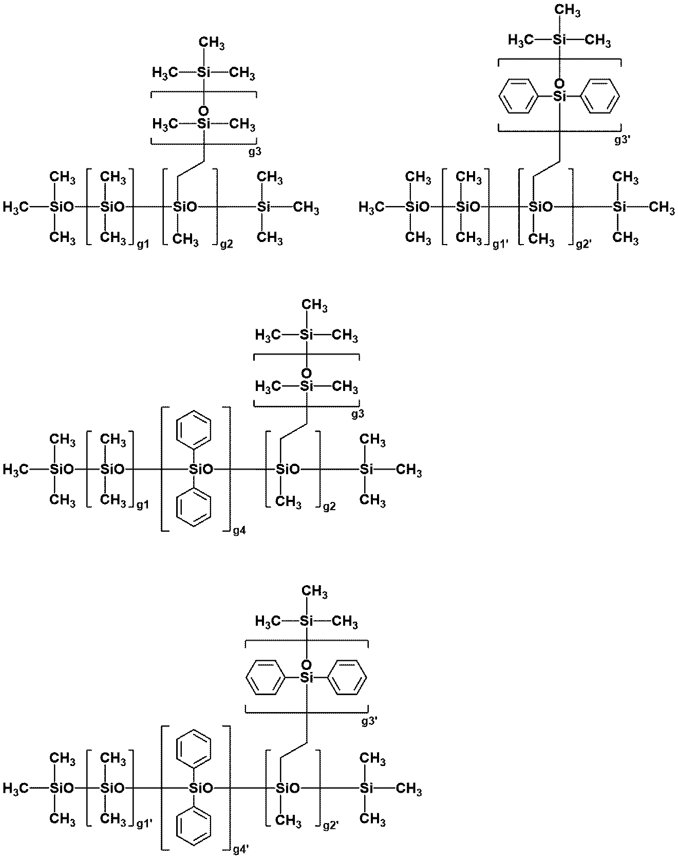

(D)成分は、ヒドロシリル化反応触媒であり、好ましくは白金族金属系ヒドロシリル化反応触媒である。(D)成分は(A)成分中のアルケニル基と、(B)成分中のヒドロシリル基との付加反応を促進する触媒である。このヒドロシリル化反応触媒は、一般に貴金属の化合物であり、高価格であることから、比較的入手しやすい白金又は白金化合物がよく用いられる。 [(D) component]
The component (D) is a hydrosilylation reaction catalyst, preferably a platinum group metal-based hydrosilylation reaction catalyst. The component (D) is a catalyst that promotes the addition reaction between the alkenyl group in the component (A) and the hydrosilyl group in the component (B). This hydrosilylation reaction catalyst is generally a compound of a noble metal, and since it is expensive, platinum or a platinum compound which is relatively easily available is often used.
前記熱硬化性シリコーン樹脂組成物は、更に(E)成分として反応制御剤を含んでもよい。反応制御剤は、組成物を調製したり、基材に塗布したりする際に、組成物が増粘やゲル化を起こさないようにするために必要に応じて任意に添加するものである。 [(E) component]
The thermosetting silicone resin composition may further contain a reaction control agent as the component (E). The reaction control agent is optionally added when the composition is prepared or applied to the base material in order to prevent the composition from thickening or gelling.
本発明の薄型ウエハの製造方法は、半導体回路等を有するウエハと支持体との仮接着に、前記ウエハ加工用仮接着剤を用いることを特徴とするものである。 [Manufacturing method of thin wafer]
The method for manufacturing a thin wafer of the present invention is characterized in that the temporary adhesive for wafer processing is used for temporary bonding between a wafer having a semiconductor circuit or the like and a support.
[工程(a)]
工程(a)は、仮接着工程であり、表面に回路形成面及び裏面に回路非形成面を有するウエハの回路形成面を、前記ウエハ加工用仮接着剤を用いて支持体に剥離可能に接着し、ウエハ積層体を形成する工程である。 The method for producing a thin wafer of the present invention includes the following steps (a) to (e).
[Step (a)]
The step (a) is a temporary bonding step, in which the circuit forming surface of the wafer having the circuit forming surface on the front surface and the circuit non-forming surface on the back surface is detachably bonded to the support using the temporary adhesive for wafer processing. This is a step of forming a wafer laminate.
工程(b)は、仮接着剤層を熱硬化させる工程である。前記ウエハ積層体を形成した後、好ましくは50~300℃、より好ましくは100~200℃で、好ましくは1分~4時間、より好ましくは5分~2時間加熱することによって、仮接着剤層の硬化を行う。 [Step (b)]
The step (b) is a step of thermosetting the temporary adhesive layer. After forming the wafer laminate, the temporary adhesive layer is preferably heated at 50 to 300 ° C., more preferably 100 to 200 ° C., preferably 1 minute to 4 hours, more preferably 5 minutes to 2 hours. Harden.
工程(c)は、支持体と仮接着したウエハの回路非形成面を研削又は研磨する工程、すなわち、前記工程で得られたウエハ積層体のウエハ裏面側を研削して、該ウエハの厚みを薄くしていく工程である。ウエハ裏面の研削加工の方式には特に制限はなく、公知の研削方式が採用される。研削は、ウエハと砥石(ダイヤモンド等)に水をかけて冷却しながら行うことが好ましい。ウエハ裏面を研削加工する装置としては、例えば(株)ディスコ製DAG-810(商品名)等が挙げられる。また、ウエハ裏面側を化学機械研磨(CMP)してもよい。 [Step (c)]
The step (c) is a step of grinding or polishing the circuit non-formed surface of the wafer temporarily bonded to the support, that is, grinding the back surface side of the wafer of the wafer laminate obtained in the step to reduce the thickness of the wafer. This is the process of thinning. The method for grinding the back surface of the wafer is not particularly limited, and a known grinding method is adopted. Grinding is preferably performed while cooling the wafer and the grindstone (diamond or the like) with water. Examples of the apparatus for grinding the back surface of the wafer include DAG-810 (trade name) manufactured by Disco Corporation. Further, the back surface side of the wafer may be chemically mechanically polished (CMP).
工程(d)は、工程(c)で回路非形成面を研削したウエハ積層体の回路非形成面に加工を施す工程である。すなわち、裏面研削によって薄型化されたウエハ積層体のウエハの回路非形成面に加工を施す工程である。この工程には、ウエハレベルで用いられる様々なプロセスが含まれる。例としては、電極形成、金属配線形成、保護膜形成等が挙げられる。より具体的には、電極等の形成のための金属スパッタリング、金属スパッタリング層をエッチングするウェットエッチング、金属配線形成のマスクとするためのレジストの塗布、露光、及び現像によるパターンの形成、レジストの剥離、ドライエッチング、金属めっきの形成、TSV形成のためのシリコンエッチング、シリコン表面の酸化膜形成など、従来公知のプロセスが挙げられる。 [Step (d)]
The step (d) is a step of processing the circuit non-formed surface of the wafer laminate obtained by grinding the circuit non-formed surface in the step (c). That is, it is a step of processing the circuit non-formed surface of the wafer of the wafer laminate thinned by backside grinding. This process involves various processes used at the wafer level. Examples include electrode formation, metal wiring formation, protective film formation, and the like. More specifically, metal sputtering for forming electrodes and the like, wet etching for etching a metal sputtering layer, application of a resist for forming a mask for metal wiring, pattern formation by exposure and development, and peeling of the resist. , Dry etching, metal plating formation, silicon etching for TSV formation, oxide film formation on the silicon surface, and the like.
工程(e)は、工程(d)で加工を施したウエハを支持体から剥離する工程、すなわち、薄型化したウエハに様々な加工を施した後、ダイシングする前にウエハを支持体から剥離する工程である。この剥離工程としては、一般に、室温から60℃程度の比較的温和な条件で実施される。剥離方法としては、ウエハ積層体のウエハ又は支持体の一方を水平に固定しておき、他方を水平方向から一定の角度を付けて持ち上げる方法、研削されたウエハの研削面に保護フィルムを貼り、ウエハと保護フィルムをピール方式でウエハ積層体から剥離する方法等が挙げられる。これらの剥離方法で剥離工程を行う場合は、通常、室温で実施される。 [Step (e)]
The step (e) is a step of peeling the wafer processed in the step (d) from the support, that is, after performing various processing on the thinned wafer, the wafer is peeled from the support before dicing. It is a process. This peeling step is generally carried out under relatively mild conditions of about room temperature to about 60 ° C. As a peeling method, one of the wafer or the support of the wafer laminate is fixed horizontally and the other is lifted at a certain angle from the horizontal direction, or a protective film is attached to the ground surface of the ground wafer. Examples thereof include a method of peeling the wafer and the protective film from the wafer laminate by a peel method. When the peeling step is performed by these peeling methods, it is usually carried out at room temperature.
(e1)加工を施したウエハのウエハ面にダイシングテープを貼付する工程、
(e2)ダイシングテープ面を吸着面に真空吸着する工程、及び
(e3)吸着面の温度が10~100℃の範囲で、支持体を、加工を施したウエハからピールオフにて剥離する工程
を含むことが好ましい。このようにすることで、支持体を、加工を施したウエハから容易に剥離することができ、また、後のダイシング工程を容易に行うことができる。 In addition, the step (e) is
(E1) A step of attaching a dicing tape to the wafer surface of the processed wafer,
(E2) includes a step of vacuum-adsorbing the dicing tape surface to the suction surface, and (e3) a step of peeling off the support from the processed wafer when the temperature of the suction surface is in the range of 10 to 100 ° C. Is preferable. By doing so, the support can be easily peeled off from the processed wafer, and the subsequent dicing step can be easily performed.
(f)剥離したウエハの回路形成面に残存する仮接着剤層を除去する工程
を行うことが好ましい。工程(e)により支持体より剥離されたウエハの回路形成面には、仮接着剤層が一部残存している場合があり、該仮接着剤層の除去は、例えば、ウエハを洗浄することにより行うことができる。 Also, after step (e),
(F) It is preferable to perform a step of removing the temporary adhesive layer remaining on the circuit forming surface of the peeled wafer. A part of the temporary adhesive layer may remain on the circuit forming surface of the wafer peeled off from the support in the step (e), and the removal of the temporary adhesive layer is, for example, cleaning the wafer. Can be done by.
[調製例1]
2.5モル%のビニル基を分子側鎖に有し、Mnが3万のジメチルポリシロキサン100質量部及びトルエン200質量部からなる溶液に、SiO4/2単位(Q単位)50モル%、(CH3)3SiO1/2単位(M単位)48モル%及び(CH2=CH)3SiO1/2単位(Vi単位)2モル%からなるMnが7,000のビニルメチルポリシロキサン50質量部及びトルエン100質量部からなる溶液、下記式(M-1)で表されるMnが2,800のオルガノハイドロジェンポリシロキサン230質量部、30質量%トルエン溶液の粘度(25℃)が30,000mPa・sである分子鎖両末端トリメチルシロキシ基封鎖直鎖状ジメチルポリシロキサン50質量部及びトルエン120質量部からなる溶液、並びに1-エチニルシクロヘキサノール0.6質量部を添加し、混合した。さらに、そこへヒドロシリル化反応触媒CAT-PL-5(信越化学工業(株)製、白金濃度1.0質量%(以下同様))を0.4質量部添加し、0.2μmのメンブレンフィルターで濾過して、熱硬化性シリコーン樹脂溶液A1を調製した。樹脂溶液A1の25℃における粘度は、230mPa・sであった。
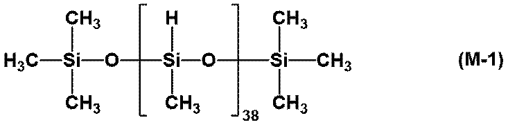
In a solution consisting of 100 parts by mass of dimethylpolysiloxane and 200 parts by mass of toluene having 2.5 mol% vinyl group in the molecular side chain and Mn of 30,000, 50 mol% of SiO 4/2 unit (Q unit), Vinyl methyl polysiloxane 50 with Mn of 7,000 consisting of (CH 3 ) 3 SiO 1/2 unit (M unit) 48 mol% and (CH 2 = CH) 3 SiO 1/2 unit (Vi unit) 2 mol% A solution consisting of 100 parts by mass and 100 parts by mass of toluene, 230 parts by mass of an organohydrogenpolysiloxane having a Mn of 2,800 represented by the following formula (M-1), and a 30 mass% toluene solution having a viscosity (25 ° C.) of 30. A solution consisting of 50 parts by mass of linear dimethylpolysiloxane and 120 parts by mass of toluene and 0.6 parts by mass of 1-ethynylcyclohexanol were added and mixed. Further, 0.4 parts by mass of a hydrosilylation reaction catalyst CAT-PL-5 (manufactured by Shin-Etsu Chemical Industry Co., Ltd., platinum concentration 1.0% by mass (same below)) was added thereto, and a 0.2 μm membrane filter was used. The mixture was filtered to prepare a thermosetting silicone resin solution A1. The viscosity of the resin solution A1 at 25 ° C. was 230 mPa · s.
2.5モル%のビニル基を分子側鎖に有し、Mnが3万のジメチルポリシロキサン70質量部、0.15モル%のビニル基を両末端鎖に有し、Mnが6万のジメチルポリシロキサン30質量部及びトルエン200質量部からなる溶液に、SiO4/2単位(Q単位)50モル%、(CH3)3SiO1/2単位(M単位)48モル%及び(CH2=CH)3SiO1/2単位(Vi単位)2モル%からなるMnが7,000のビニルメチルポリシロキサン50質量部及びトルエン100質量部からなる溶液、式(M-1)で表されるMnが2,800のオルガノハイドロジェンポリシロキサン180質量部、30質量%トルエン溶液の粘度(25℃)が1,000mPa・sである分子鎖両末端トリメチルシロキシ基封鎖直鎖状ジメチルポリシロキサン30質量部、並びに1-エチニルシクロヘキサノール0.6質量部を添加し、混合した。さらに、そこへヒドロシリル化反応触媒CAT-PL-5を0.4質量部添加し、0.2μmのメンブレンフィルターで濾過して、熱硬化性シリコーン樹脂溶液A2を調製した。樹脂溶液A2の25℃における粘度は、100mPa・sであった。 [Preparation Example 2]
Dimethyl having 2.5 mol% vinyl group in the molecular side chain, 70 parts by mass of dimethylpolysiloxane with Mn of 30,000, and vinyl group of 0.15 mol% in both terminal chains, Mn of 60,000. In a solution consisting of 30 parts by mass of polysiloxane and 200 parts by mass of toluene, SiO 4/2 unit (Q unit) 50 mol%, (CH 3 ) 3 SiO 1/2 unit (M unit) 48 mol% and (CH 2 =) CH) 3 A solution consisting of 50 parts by mass of vinyl methyl polysiloxane and 100 parts by mass of toluene having an Mn of 7,000 in an amount of 2 mol% of 1 1/2 unit (Vi unit), expressed by the formula (M-1). Is 2,800 parts by mass of organohydrogenpolysiloxane, and the viscosity (25 ° C.) of the 30% by mass toluene solution is 1,000 mPa · s. , And 0.6 parts by mass of 1-ethynylcyclohexanol were added and mixed. Further, 0.4 parts by mass of the hydrosilylation reaction catalyst CAT-PL-5 was added thereto, and the mixture was filtered through a 0.2 μm membrane filter to prepare a thermosetting silicone resin solution A2. The viscosity of the resin solution A2 at 25 ° C. was 100 mPa · s.
2.5モル%のビニル基を分子の両末端及び側鎖に有し、Mnが3万のジメチルポリシロキサン100質量部及びトルエン200質量部からなる溶液に、SiO4/2単位(Q単位)50モル%、(CH3)3SiO1/2単位(M単位)48モル%及び(CH2=CH)3SiO1/2単位(Vi単位)2モル%からなるMnが7,000のビニルメチルポリシロキサン50質量部及びトルエン100質量部からなる溶液、式(M-1)で表されるMnが2,800のオルガノハイドロジェンポリシロキサン230質量部、30質量%トルエン溶液の粘度(25℃)が100,000mPa・sである分子鎖両末端トリメチルシロキシ基封鎖直鎖状ジメチルポリシロキサン20質量部及びトルエン300質量部からなる溶液、並びに1-エチニルシクロヘキサノール0.6質量部を添加し、混合した。さらに、そこへヒドロシリル化反応触媒CAT-PL-5を0.4質量部添加し、0.2μmのメンブレンフィルターで濾過して、熱硬化性シリコーン樹脂溶液A3を調製した。樹脂溶液A3の25℃における粘度は、330mPa・sであった。 [Preparation Example 3]
4/2 units of SiO (Q units) in a solution consisting of 100 parts by mass of dimethylpolysiloxane and 200 parts by mass of toluene having 2.5 mol% vinyl groups at both ends and side chains of the molecule and Mn of 30,000. Vinyl with Mn of 7,000 consisting of 50 mol%, (CH 3 ) 3 SiO 1/2 unit (M unit) 48 mol% and (CH 2 = CH) 3 SiO 1/2 unit (Vi unit) 2 mol% A solution consisting of 50 parts by mass of methylpolysiloxane and 100 parts by mass of toluene, 230 parts by mass of organohydrogenpolysiloxane having a Mn of 2,800 represented by the formula (M-1), and a viscosity (25 ° C.) of a 30% by mass toluene solution. ) Is 100,000 mPa · s, a solution consisting of 20 parts by mass of linear dimethylpolysiloxane and 300 parts by mass of toluene, and 0.6 parts by mass of 1-ethynylcyclohexanol were added. Mixed. Further, 0.4 parts by mass of the hydrosilylation reaction catalyst CAT-PL-5 was added thereto, and the mixture was filtered through a 0.2 μm membrane filter to prepare a thermosetting silicone resin solution A3. The viscosity of the resin solution A3 at 25 ° C. was 330 mPa · s.
2.5モル%のビニル基を分子の両末端及び側鎖に有し、Mnが3万のジメチルポリシロキサン100質量部及びトルエン200質量部からなる溶液に、SiO4/2単位(Q単位)50モル%、(CH3)3SiO1/2単位(M単位)48モル%及び(CH2=CH)3SiO1/2単位(Vi単位)2モル%からなるMnが7,000のビニルメチルポリシロキサン200質量部及びトルエン400質量部からなる溶液、式(M-1)で表されるMnが2,800のオルガノハイドロジェンポリシロキサン430質量部、30質量%トルエン溶液の粘度(25℃)が30,000mPa・sである分子鎖両末端トリメチルシロキシ基封鎖直鎖状ジメチルポリシロキサン100質量部及びトルエン120質量部からなる溶液、並びに1-エチニルシクロヘキサノール1.2質量部を添加し、混合した。さらに、そこへヒドロシリル化反応触媒CAT-PL-5を0.8質量部添加し、0.2μmのメンブレンフィルターで濾過して、熱硬化性シリコーン樹脂溶液A4を調製した。樹脂溶液A4の25℃における粘度は、120mPa・sであった。 [Preparation Example 4]
4/2 units of SiO (Q units) in a solution consisting of 100 parts by mass of dimethylpolysiloxane and 200 parts by mass of toluene having 2.5 mol% vinyl groups at both ends and side chains of the molecule and Mn of 30,000. Vinyl with Mn of 7,000 consisting of 50 mol%, (CH 3 ) 3 SiO 1/2 unit (M unit) 48 mol% and (CH 2 = CH) 3 SiO 1/2 unit (Vi unit) 2 mol% A solution consisting of 200 parts by mass of methylpolysiloxane and 400 parts by mass of toluene, 430 parts by mass of organohydrogenpolysiloxane having a Mn of 2,800 represented by the formula (M-1), and a viscosity (25 ° C.) of a 30% by mass toluene solution. ) Is 30,000 mPa · s, a solution consisting of 100 parts by mass of linear dimethylpolysiloxane and 120 parts by mass of toluene, and 1.2 parts by mass of 1-ethynylcyclohexanol were added. Mixed. Further, 0.8 parts by mass of the hydrosilylation reaction catalyst CAT-PL-5 was added thereto, and the mixture was filtered through a 0.2 μm membrane filter to prepare a thermosetting silicone resin solution A4. The viscosity of the resin solution A4 at 25 ° C. was 120 mPa · s.
2.5モル%のビニル基を分子側鎖に有し、Mnが3万のジメチルポリシロキサン70質量部、0.15モル%のビニル基を両末端鎖に有し、Mnが6万のジメチルポリシロキサン30質量部及びトルエン200質量部からなる溶液に、SiO4/2単位(Q単位)50モル%、(CH3)3SiO1/2単位(M単位)48モル%及び(CH2=CH)3SiO1/2単位(Vi単位)2モル%からなるMnが7,000のビニルメチルポリシロキサン200質量部及びトルエン400質量部からなる溶液、式(M-1)で表されるMnが2,800のオルガノハイドロジェンポリシロキサン380質量部、30質量%トルエン溶液の粘度(25℃)が1,000mPa・sである分子鎖両末端トリメチルシロキシ基封鎖直鎖状ジメチルポリシロキサン150質量部、並びに1-エチニルシクロヘキサノール1.2質量部を添加し、混合した。さらに、そこへヒドロシリル化反応触媒CAT-PL-5を0.8質量部添加し、0.2μmのメンブレンフィルターで濾過して、熱硬化性シリコーン樹脂溶液A5を調製した。樹脂溶液A5の25℃における粘度は、80mPa・sであった。 [Preparation Example 5]
Dimethyl having 2.5 mol% vinyl group in the molecular side chain, 70 parts by mass of dimethylpolysiloxane with Mn of 30,000, and vinyl group of 0.15 mol% in both terminal chains, Mn of 60,000. In a solution consisting of 30 parts by mass of polysiloxane and 200 parts by mass of toluene, SiO 4/2 unit (Q unit) 50 mol%, (CH 3 ) 3 SiO 1/2 unit (M unit) 48 mol% and (CH 2 =) CH) A solution consisting of 200 parts by mass of vinyl methyl polysiloxane and 400 parts by mass of toluene having an Mn of 7,000 in 2 mol% of 3 SiO 1/2 unit (Vi unit), Mn represented by the formula (M-1). 380 parts by mass of organohydrogenpolysiloxane with 2,800, and 150 parts by mass of linear dimethylpolysiloxane with trimethylsiloxy group closure at both ends of the molecular chain having a viscosity (25 ° C.) of a 30 mass% toluene solution of 1,000 mPa · s. , And 1.2 parts by mass of 1-ethynylcyclohexanol were added and mixed. Further, 0.8 parts by mass of the hydrosilylation reaction catalyst CAT-PL-5 was added thereto, and the mixture was filtered through a 0.2 μm membrane filter to prepare a thermosetting silicone resin solution A5. The viscosity of the resin solution A5 at 25 ° C. was 80 mPa · s.
2.5モル%のビニル基を分子側鎖に有し、Mnが3万のジメチルポリシロキサン100質量部及びトルエン200質量部からなる溶液に、SiO4/2単位(Q単位)50モル%、(CH3)3SiO1/2単位(M単位)48モル%及び(CH2=CH)3SiO1/2単位(Vi単位)2モル%からなるMnが7,000のビニルメチルポリシロキサン50質量部及びトルエン100質量部からなる溶液、式(M-1)で表されるMnが2,800のオルガノハイドロジェンポリシロキサン230質量部、下記式(M-2)で表される30質量%トルエン溶液の粘度(25℃)が50,000mPa・sである分子鎖末端トリメチルシロキシ基封鎖分岐状ポリシロキサン50質量部及びトルエン120質量部からなる溶液、並びに1-エチニルシクロヘキサノール0.6質量部を添加し、混合した。さらに、そこへヒドロシリル化反応触媒CAT-PL-5を0.4質量部添加し、0.2μmのメンブレンフィルターで濾過して、熱硬化性シリコーン樹脂溶液A6を調製した。樹脂溶液A6の25℃における粘度は、360mPa・sであった。
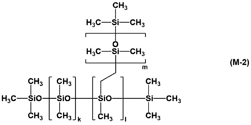
In a solution consisting of 100 parts by mass of dimethylpolysiloxane and 200 parts by mass of toluene having 2.5 mol% vinyl group in the molecular side chain and Mn of 30,000, 50 mol% of SiO 4/2 unit (Q unit), Vinyl methyl polysiloxane 50 with Mn of 7,000 consisting of (CH 3 ) 3 SiO 1/2 unit (M unit) 48 mol% and (CH 2 = CH) 3 SiO 1/2 unit (Vi unit) 2 mol% A solution consisting of 100 parts by mass and 100 parts by mass of toluene, 230 parts by mass of an organohydrogenpolysiloxane having a Mn of 2,800 represented by the formula (M-1), and 30% by mass represented by the following formula (M-2). A solution consisting of 50 parts by mass of a branched polysiloxane having a molecular chain-terminated trimethylsiloxy group-blocked branched polysiloxane having a viscosity (25 ° C.) of 50,000 mPa · s and 120 parts by mass of toluene, and 0.6 parts by mass of 1-ethynylcyclohexanol. Was added and mixed. Further, 0.4 parts by mass of the hydrosilylation reaction catalyst CAT-PL-5 was added thereto, and the mixture was filtered through a 0.2 μm membrane filter to prepare a thermosetting silicone resin solution A6. The viscosity of the resin solution A6 at 25 ° C. was 360 mPa · s.
2.5モル%のビニル基を分子の両末端及び側鎖に有し、Mnが3万のジメチルポリシロキサン100質量部及びトルエン200質量部からなる溶液に、SiO4/2単位(Q単位)50モル%、(CH3)3SiO1/2単位(M単位)48モル%及び(CH2=CH)3SiO1/2単位(Vi単位)2モル%からなるMnが7,000のビニルメチルポリシロキサン200質量部及びトルエン400質量部からなる溶液、式(M-1)で表されるMnが2,800のオルガノハイドロジェンポリシロキサン430質量部、式(M-2)で表される30質量%トルエン溶液の粘度(25℃)が50,000mPa・sである分子鎖末端トリメチルシロキシ基封鎖分岐状ポリシロキサン100質量部及びトルエン120質量部からなる溶液、並びに1-エチニルシクロヘキサノール1.2質量部を添加し、混合した。さらに、そこへヒドロシリル化反応触媒CAT-PL-5を0.8質量部添加し、0.2μmのメンブレンフィルターで濾過して、熱硬化性シリコーン樹脂溶液A7を調製した。樹脂溶液A7の25℃における粘度は、280mPa・sであった。 [Preparation Example 7]
4/2 units of SiO (Q units) in a solution consisting of 100 parts by mass of dimethylpolysiloxane and 200 parts by mass of toluene having 2.5 mol% vinyl groups at both ends and side chains of the molecule and Mn of 30,000. Vinyl with Mn of 7,000 consisting of 50 mol%, (CH 3 ) 3 SiO 1/2 unit (M unit) 48 mol% and (CH 2 = CH) 3 SiO 1/2 unit (Vi unit) 2 mol% A solution consisting of 200 parts by mass of methylpolysiloxane and 400 parts by mass of toluene, 430 parts by mass of organohydrogenpolysiloxane having a Mn of 2,800 represented by the formula (M-1), represented by the formula (M-2). A solution consisting of 100 parts by mass of a branched polysiloxane having a molecular chain-terminated trimethylsiloxy group-blocking branched polysiloxane having a viscosity (25 ° C.) of 50,000 mPa · s and 120 parts by mass of toluene, and 1-ethynylcyclohexanol 1. 2 parts by mass was added and mixed. Further, 0.8 parts by mass of the hydrosilylation reaction catalyst CAT-PL-5 was added thereto, and the mixture was filtered through a 0.2 μm membrane filter to prepare a thermosetting silicone resin solution A7. The viscosity of the resin solution A7 at 25 ° C. was 280 mPa · s.
分子鎖両末端トリメチルシロキシ基封鎖直鎖状ジメチルポリシロキサン50質量部及びトルエン120質量部からなる溶液を添加しなかったこと以外は、調製例1と同様の方法で熱硬化性シリコーン樹脂溶液CA1を調製した。樹脂溶液CA1の25℃における粘度は、150mPa・sであった。 [Comparative Preparation Example 1]
Thermosetting silicone resin solution CA1 was prepared in the same manner as in Preparation Example 1 except that a solution consisting of 50 parts by mass of linear dimethylpolysiloxane and 120 parts by mass of toluene was added. Prepared. The viscosity of the resin solution CA1 at 25 ° C. was 150 mPa · s.
分子鎖両末端トリメチルシロキシ基封鎖直鎖状ジメチルポリシロキサン30質量部を添加しなかったこと以外は、調製例2と同様の方法で熱硬化性シリコーン樹脂溶液CA2を調製した。樹脂溶液CA2の25℃における粘度は、180mPa・sであった。 [Comparative Preparation Example 2]
A thermosetting silicone resin solution CA2 was prepared in the same manner as in Preparation Example 2 except that 30 parts by mass of linear dimethylpolysiloxane was not added. The viscosity of the resin solution CA2 at 25 ° C. was 180 mPa · s.
分子鎖両末端トリメチルシロキシ基封鎖直鎖状ジメチルポリシロキサン50質量部を、下記式(M-3)で表される側鎖にエポキシ基を含むポリシロキサン(30質量%トルエン溶液の粘度(25℃):33,000mPa・s)50質量部に変更したこと以外は、調製例1と同様の方法で熱硬化性シリコーン樹脂溶液CA3を調製した。樹脂溶液CA3の25℃における粘度は、260mPa・sであった。

Polysiloxane (30 mass% toluene solution viscosity (25 ° C.)) containing 50 parts by mass of linear dimethylpolysiloxane with trimethylsiloxy group closure at both ends of the molecular chain and an epoxy group in the side chain represented by the following formula (M-3). ): 33,000 mPa · s) A thermosetting silicone resin solution CA3 was prepared in the same manner as in Preparation Example 1 except that it was changed to 50 parts by mass. The viscosity of the resin solution CA3 at 25 ° C. was 260 mPa · s.
分子鎖両末端トリメチルシロキシ基封鎖直鎖状ジメチルポリシロキサン30質量部を、下記式(M-4)で表される側鎖にトリメトキシシリル基を含むポリシロキサン(30質量%トルエン溶液の粘度(25℃):2,500mPa・s)30質量部に変更したこと以外は、調製例2同様の方法で熱硬化性シリコーン樹脂溶液CA4を調製した。樹脂溶液CA4の25℃における粘度は、190mPa・sであった。
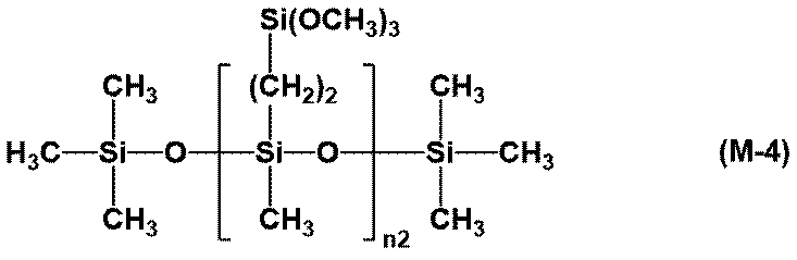
30 parts by mass of linear dimethylpolysiloxane sealed with trimethylsiloxy group at both ends of the molecular chain, and polysiloxane containing a trimethoxysilyl group in the side chain represented by the following formula (M-4) (viscosity of a 30 mass% toluene solution (30 mass% toluene solution) 25 ° C.): 2,500 mPa · s) A thermosetting silicone resin solution CA4 was prepared in the same manner as in Preparation Example 2 except that it was changed to 30 parts by mass. The viscosity of the resin solution CA4 at 25 ° C. was 190 mPa · s.
[実施例1~7及び比較例1~4]
表面に高さ10μm、直径40μmの銅ポストが全面に形成された直径200mmのシリコンウエハ(厚さ:725μm)上に、熱硬化性シリコーン樹脂溶液A1~A7及びCA1~CA4をそれぞれスピンコートし、ホットプレートにて100℃で2分間加熱して、下記表1及び2に示す膜厚で仮接着剤層をウエハバンプ形成面に成膜した。直径200mm(厚さ:500μm)のガラス板を支持体として、仮接着剤層を有するシリコンウエハ及びガラス板をそれぞれ、仮接着剤層とガラス板が合わさるように、EVG社のウエハ接合装置EVG520ISを用いて100℃、10-3mbar以下、荷重5kNにて真空貼り合わせを行い、ウエハ積層体を作製した。なお、基板接着後の異常を目視で判別するために支持体としてガラス板を使用したが、ウエハ等の光を透過しないシリコン基板も使用可能である。 [2] Preparation of wafer laminate and its evaluation [Examples 1 to 7 and Comparative Examples 1 to 4]
Thermosetting silicone resin solutions A1 to A7 and CA1 to CA4 were spin-coated on a silicon wafer (thickness: 725 μm) having a diameter of 200 mm and a copper post having a height of 10 μm and a diameter of 40 μm formed on the entire surface. The temporary adhesive layer was formed on the wafer bump forming surface with the film thickness shown in Tables 1 and 2 below by heating at 100 ° C. for 2 minutes on a hot plate. Using a glass plate with a diameter of 200 mm (thickness: 500 μm) as a support, a silicon wafer having a temporary adhesive layer and a glass plate are respectively combined with an EVG wafer bonding device EVG520IS so that the temporary adhesive layer and the glass plate are combined. Wafer laminates were prepared by vacuum bonding at 100 ° C., 10 -3 mbar or less, and a load of 5 kN. Although a glass plate is used as a support for visually discriminating abnormalities after bonding the substrates, a silicon substrate such as a wafer that does not transmit light can also be used.
前記ウエハ積層体を180℃で1時間オーブンを用いて加熱し、室温まで冷却した後、ウエハ界面の接着状況を目視で確認し、界面に気泡等の異常が発生しなかった場合を良好と評価して「○」で示し、異常が発生した場合を不良と評価して「×」で示した。 (1) Adhesiveness test After heating the wafer laminate at 180 ° C. for 1 hour in an oven and cooling it to room temperature, the adhesion status of the wafer interface was visually confirmed, and no abnormalities such as air bubbles occurred at the interface. The case was evaluated as good and indicated by "○", and the case where an abnormality occurred was evaluated as defective and indicated by "x".
前記ウエハ積層体を用いて、グラインダー((株)ディスコ製DAG-810)でダイヤモンド砥石を用いてシリコンウエハの裏面研削を行った。基板の厚さが50μmになるまでグラインドした後、光学顕微鏡(100倍)にてクラック、剥離等の異常の有無を調べた。異常が発生しなかった場合を良好と評価して「○」で示し、異常が発生した場合を不良と評価して「×」で示した。 (2) Backside Grinding Resistance Test Using the wafer laminate, the backside of a silicon wafer was ground with a grinder (DAG-810 manufactured by Disco Co., Ltd.) using a diamond grindstone. After grinding until the thickness of the substrate became 50 μm, the presence or absence of abnormalities such as cracks and peeling was examined with an optical microscope (100 times). When no abnormality occurred, it was evaluated as good and indicated by "○", and when an abnormality occurred, it was evaluated as defective and indicated by "x".
(2)裏面研削耐性試験を終えた後のウエハ積層体をCVD装置に導入し、2μmのSiO2膜の成膜実験を行い、その際の外観異常の有無を目視観察によって調べた。外観異常が発生しなかった場合を良好と評価して「○」で示し、ボイド、ウエハ膨れ、ウエハ破損等の外観異常が発生した場合を不良と評価して「×」で示した。CVD耐性試験の条件は、以下のとおりである。
装置名:サムコ(株)製プラズマCVD、PD270STL
RF500W、内圧40Pa
TEOS(テトラエチルオルソシリケート):O2=20sccm:680sccm (3) CVD resistance test (2) After the back surface grinding resistance test is completed, the wafer laminate is introduced into the CVD device, a film formation experiment of a 2 μm SiO 2 film is performed, and the presence or absence of an appearance abnormality at that time is visually observed. Investigated by. The case where no appearance abnormality occurred was evaluated as good and indicated by "○", and the case where appearance abnormality such as voids, wafer swelling, and wafer breakage occurred was evaluated as defective and indicated by "x". The conditions for the CVD resistance test are as follows.
Device name: Plasma CVD, PD270STL manufactured by SAMCO Co., Ltd.
RF500W, internal pressure 40Pa
TEOS (Tetraethyl Orthosilicate): O 2 = 20 sccm: 680 sccm
基板の剥離性は、まず、(3)CVD耐性試験を終えたウエハ積層体のウエハ側にダイシングフレームを用いてダイシングテープ(日東電工(株)製ELP UB-3083D)を貼り、このダイシングテープ面を真空吸着によって、吸着板にセットした。その後、室温にて、ガラスの1点をピンセットにて持ち上げることで、ガラス基板を剥離した。50μm厚のウエハを割ることなく剥離できた場合を「○」で示し、割れ等の異常が発生した場合を不良と評価して「×」で示した。 (4) Peelability test For the peelability of the substrate, first, (3) use a dicing frame on the wafer side of the wafer laminate that has undergone the CVD resistance test, and apply a dicing tape (ELP UB-3083D manufactured by Nitto Denko Corporation). The dicing tape surface was attached and set on the adsorption plate by vacuum adsorption. Then, at room temperature, one point of the glass was lifted with tweezers to peel off the glass substrate. The case where the wafer having a thickness of 50 μm could be peeled off without breaking was indicated by “◯”, and the case where an abnormality such as cracking occurred was evaluated as defective and indicated by “x”.
(4)剥離性試験終了後のダイシングテープを介してダイシングフレームに装着された直径200mmウエハ(CVD耐性試験条件に晒されたもの)を、剥離面を上にしてスピンコーターにセットし、洗浄溶剤としてSPIS-TA-CLEANER 25(信越化学工業(株)製)を5分間噴霧したのち、ウエハを回転させながらイソプロピルアルコール(IPA)を噴霧してリンスを行った。その後、外観を観察して残存する接着剤の有無を目視でチェックした。樹脂の残存が認められないものを良好と評価して「○」で示し、樹脂の残存が認められたものを不良と評価して「×」で示した。 (5) Cleaning and removability test (4) A wafer with a diameter of 200 mm (exposed to CVD resistance test conditions) mounted on a dicing frame via a dicing tape after the peelability test is spun with the peeling surface facing up. The wafer was set on a coater and SPIS-TA-CLEANER 25 (manufactured by Shin-Etsu Chemical Co., Ltd.) was sprayed as a cleaning solvent for 5 minutes, and then isopropyl alcohol (IPA) was sprayed and rinsed while rotating the wafer. After that, the appearance was observed and the presence or absence of residual adhesive was visually checked. Those with no residual resin were evaluated as good and indicated by "○", and those with residual resin were evaluated as defective and indicated by "x".
直径200mmのシリコンウエハ(厚さ:725μm)上に熱硬化性シリコーン樹脂溶液A1~A7及びCA1~CA4をそれぞれスピンコートし、ホットプレートにて100℃で2分間加熱することで、表1及び2に示す膜厚でウエハバンプ形成面にシリコーン樹脂層を成膜した。その後、オーブンにて180℃で1時間かけてシリコーン樹脂層を硬化させ、室温まで冷却した後、前記ウエハ上のシリコーン樹脂層上に150mm長×25mm幅のポリイミドテープを5本貼り付け、テープが貼られていない部分の仮接着剤層を除去した。(株)島津製作所のAUTOGRAPH (AG-1)を用いて25℃、300mm/分の速度でテープの一端から180°剥離で120mm剥がし、そのときにかかる力の平均(120mmストローク×5回)を、そのシリコーン樹脂層のピール剥離力とした。 (6) Peel peeling force test A thermosetting silicone resin solutions A1 to A7 and CA1 to CA4 are spin-coated on a silicon wafer (thickness: 725 μm) having a diameter of 200 mm, and heated on a hot plate at 100 ° C. for 2 minutes. As a result, a silicone resin layer was formed on the wafer bump forming surface with the film thicknesses shown in Tables 1 and 2. Then, the silicone resin layer was cured at 180 ° C. for 1 hour in an oven, cooled to room temperature, and then five 150 mm long × 25 mm wide polyimide tapes were attached onto the silicone resin layer on the wafer to form the tape. The temporary adhesive layer on the unattached part was removed. Using AUTOGRAPH (AG-1) from Shimadzu Corporation, peel 120 mm from one end of the tape at a speed of 300 mm / min at 25 ° C by 180 ° peeling, and average the force applied at that time (120 mm stroke x 5 times). , The peel peeling force of the silicone resin layer.
ガラス基板上に熱硬化性シリコーン樹脂溶液A1~A7及びCA1~CA4をそれぞれスピンコートし、ホットプレートにて100℃で2分間加熱することで、表1及び2に示す膜厚でガラス基板上にシリコーン樹脂層を成膜した。その後、オーブンにて180℃で1時間かけてシリコーン樹脂層を硬化させ、室温まで冷却した。得られたシリコーン樹脂層を含むガラス基板を、TAインスツルメント社製レオメーター(アレスG2)を使用し、シリコーン樹脂層に50gfの荷重がかかるよう25mmアルミニウムプレートで挟んだ状態で25℃、1Hzで弾性率測定を行い、得られた貯蔵弾性率の値をシリコーン樹脂層の貯蔵弾性率とした。 (7) Measurement of storage elastic modulus The thermosetting silicone resin solutions A1 to A7 and CA1 to CA4 are spin-coated on a glass substrate and heated on a hot plate at 100 ° C. for 2 minutes, as shown in Tables 1 and 2. A silicone resin layer was formed on the glass substrate with a film thickness. Then, the silicone resin layer was cured in an oven at 180 ° C. for 1 hour and cooled to room temperature. The glass substrate containing the obtained silicone resin layer was sandwiched between 25 mm aluminum plates so that a load of 50 gf was applied to the silicone resin layer using a Leometer (Ares G2) manufactured by TA Instruments, Inc. at 25 ° C., 1 Hz. The elastic modulus was measured in 1 and the value of the obtained storage elastic modulus was taken as the storage elastic modulus of the silicone resin layer.


Claims (8)
- 無官能性オルガノポリシロキサンを含む熱硬化性シリコーン樹脂組成物からなる、ウエハを支持体に仮接着するためのウエハ加工用仮接着剤。 A temporary adhesive for wafer processing for temporarily adhering a wafer to a support, which comprises a thermosetting silicone resin composition containing a non-functional organopolysiloxane.
- 前記無官能性オルガノポリシロキサンを含む熱硬化性シリコーン樹脂組成物が、
(A)1分子中に2個以上のアルケニル基を有するオルガノポリシロキサン:100質量部、
(B)1分子中に2個以上のケイ素原子に結合した水素原子(SiH基)を含有するオルガノハイドロジェンポリシロキサン:(A)成分中のアルケニル基の合計に対する(B)成分中のSiH基の合計が、モル比で0.3~10となる量、
(C)無官能性オルガノポリシロキサン:0.1~200質量部、及び
(D)ヒドロシリル化反応触媒:(A)、(B)及び(C)成分の合計質量に対し、金属原子量換算で0.1~5,000ppm
を含むものである請求項1記載のウエハ加工用仮接着剤。 The thermosetting silicone resin composition containing the non-functional organopolysiloxane
(A) Organopolysiloxane having two or more alkenyl groups in one molecule: 100 parts by mass,
(B) Organohydrogenpolysiloxane containing a hydrogen atom (SiH group) bonded to two or more silicon atoms in one molecule: SiH group in the component (B) with respect to the total number of alkenyl groups in the component (A). Amount in which the total of is 0.3 to 10 in terms of molar ratio,
(C) Non-functional organopolysiloxane: 0.1 to 200 parts by mass, and (D) Hydrosilylation reaction catalyst: 0 in terms of metal atomic weight with respect to the total mass of the components (A), (B) and (C) .1 to 5,000 ppm
The temporary adhesive for wafer processing according to claim 1. - (C)成分の無官能性オルガノポリシロキサンの30質量%トルエン溶液の25℃における粘度が、100~500,000mPa・sである請求項2記載のウエハ加工用仮接着剤。 The temporary adhesive for wafer processing according to claim 2, wherein the viscosity of a 30 mass% toluene solution of the non-functional organopolysiloxane of the component (C) at 25 ° C. is 100 to 500,000 mPa · s.
- 前記無官能性オルガノポリシロキサンを含む熱硬化性シリコーン樹脂組成物が、更に(E)成分としてヒドロシリル化反応制御剤を前記(A)、(B)及び(C)成分の合計質量に対し、0.001~10質量部含む請求項1~3のいずれか1項記載のウエハ加工用仮接着剤。 The thermosetting silicone resin composition containing the non-functional organopolysiloxane further contains a hydrosilylation reaction control agent as a component (E) at 0 with respect to the total mass of the components (A), (B) and (C). The temporary adhesive for wafer processing according to any one of claims 1 to 3, which contains .001 to 10 parts by mass.
- 前記無官能性オルガノポリシロキサンを含む熱硬化性シリコーン樹脂組成物の硬化後、25℃でのシリコン基板に対する25mm幅の試験片の180°ピール剥離力が、2gf以上50gf以下である請求項1~4のいずれか1項記載のウエハ加工用仮接着剤。 After curing the thermosetting silicone resin composition containing the non-functional organopolysiloxane, the 180 ° peel peeling force of the test piece having a width of 25 mm with respect to the silicon substrate at 25 ° C. is 2 gf or more and 50 gf or less. The temporary adhesive for wafer processing according to any one of 4.
- 前記無官能性オルガノポリシロキサンを含む熱硬化性シリコーン樹脂組成物の硬化後、25℃での貯蔵弾性率が、1,000Pa以上1,000MPa以下である請求項1~5のいずれか1項記載のウエハ加工用仮接着剤。 The method according to any one of claims 1 to 5, wherein the storage elastic modulus at 25 ° C. after curing of the thermosetting silicone resin composition containing the non-functional organopolysiloxane is 1,000 Pa or more and 1,000 MPa or less. Temporary adhesive for wafer processing.
- (a)表面に回路形成面及び裏面に回路非形成面を有するウエハの前記回路形成面を、請求項1~6のいずれか1項記載のウエハ加工用仮接着剤を用いて支持体に剥離可能に接着し、ウエハ積層体を形成する工程と、
(b)前記仮接着剤を熱硬化させる工程と、
(c)前記ウエハ積層体のウエハの回路非形成面を研削又は研磨する工程と、
(d)前記ウエハの回路非形成面に加工を施す工程と、
(e)前記加工を施したウエハを前記支持体から剥離する工程と
を含む薄型ウエハの製造方法。 (A) The circuit-forming surface of a wafer having a circuit-forming surface on the front surface and a circuit-non-forming surface on the back surface is peeled off to a support using the temporary adhesive for wafer processing according to any one of claims 1 to 6. The process of adhering as much as possible and forming a wafer laminate,
(B) A step of thermosetting the temporary adhesive and
(C) A step of grinding or polishing the circuit non-formed surface of the wafer of the wafer laminate, and
(D) A step of processing the circuit non-formed surface of the wafer and
(E) A method for manufacturing a thin wafer, which includes a step of peeling the processed wafer from the support. - 支持体と、その上に積層された請求項1~6のいずれか1項記載のウエハ加工用仮接着剤から得られる仮接着剤層と、表面に回路形成面及び裏面に回路非形成面を有するウエハとを備えるウエハ積層体であって、
前記仮接着剤層が、前記ウエハの表面に剥離可能に接着されたものであるウエハ積層体。 A temporary adhesive layer obtained from the support and the temporary adhesive for wafer processing according to any one of claims 1 to 6 laminated on the support, and a circuit-formed surface on the front surface and a circuit-non-formed surface on the back surface. A wafer laminate including a wafer to be provided.
A wafer laminate in which the temporary adhesive layer is detachably adhered to the surface of the wafer.
Priority Applications (5)
| Application Number | Priority Date | Filing Date | Title |
|---|---|---|---|
| CN202080083572.4A CN114868232A (en) | 2019-12-02 | 2020-12-01 | Temporary adhesive for wafer processing, wafer laminate, and method for producing thin wafer |
| EP20897411.3A EP4071223A4 (en) | 2019-12-02 | 2020-12-01 | Wafer processing temporary adhesive, wafer laminate, thin wafer manufacturing method |
| US17/779,199 US20230002647A1 (en) | 2019-12-02 | 2020-12-01 | Wafer processing temporary adhesive, wafer laminate, thin wafer manufacturing method |
| KR1020227022020A KR20220108799A (en) | 2019-12-02 | 2020-12-01 | Temporary adhesive for wafer processing, wafer laminate and manufacturing method of thin wafer |
| JP2021562648A JPWO2021112070A1 (en) | 2019-12-02 | 2020-12-01 |
Applications Claiming Priority (2)
| Application Number | Priority Date | Filing Date | Title |
|---|---|---|---|
| JP2019-217754 | 2019-12-02 | ||
| JP2019217754 | 2019-12-02 |
Publications (1)
| Publication Number | Publication Date |
|---|---|
| WO2021112070A1 true WO2021112070A1 (en) | 2021-06-10 |
Family
ID=76221077
Family Applications (1)
| Application Number | Title | Priority Date | Filing Date |
|---|---|---|---|
| PCT/JP2020/044638 WO2021112070A1 (en) | 2019-12-02 | 2020-12-01 | Wafer processing temporary adhesive, wafer laminate, thin wafer manufacturing method |
Country Status (7)
| Country | Link |
|---|---|
| US (1) | US20230002647A1 (en) |
| EP (1) | EP4071223A4 (en) |
| JP (1) | JPWO2021112070A1 (en) |
| KR (1) | KR20220108799A (en) |
| CN (1) | CN114868232A (en) |
| TW (1) | TW202134386A (en) |
| WO (1) | WO2021112070A1 (en) |
Cited By (1)
| Publication number | Priority date | Publication date | Assignee | Title |
|---|---|---|---|---|
| WO2022202153A1 (en) * | 2021-03-26 | 2022-09-29 | 日産化学株式会社 | Adhesive composition, layered product, method for producing layered product, and method for producing semiconductor substrate |
Citations (11)
| Publication number | Priority date | Publication date | Assignee | Title |
|---|---|---|---|---|
| JP2002060719A (en) * | 2000-08-21 | 2002-02-26 | Shin Etsu Chem Co Ltd | Adhesive silicone rubber composition and semiconductor device |
| JP2004064040A (en) | 2002-06-03 | 2004-02-26 | Three M Innovative Properties Co | Laminate including substrate to be ground, method of manufacturing the same, method of manufacturing ultrathin substrate using the laminate, and apparatus therefor |
| JP2006328104A (en) | 2005-05-23 | 2006-12-07 | Jsr Corp | Adhesive composition |
| US7541264B2 (en) | 2005-03-01 | 2009-06-02 | Dow Corning Corporation | Temporary wafer bonding method for semiconductor processing |
| JP2014118484A (en) * | 2012-12-17 | 2014-06-30 | Dow Corning Toray Co Ltd | Thermal conductive silicone composition and thermal conductive member |
| JP2016119438A (en) * | 2014-12-24 | 2016-06-30 | 信越化学工業株式会社 | Method for temporarily adhering wafer and method for manufacturing thin wafer |
| WO2017006549A1 (en) * | 2015-07-03 | 2017-01-12 | 三井化学東セロ株式会社 | Semiconductor wafer surface protection film and method for manufacturing semiconductor device |
| WO2017191815A1 (en) * | 2016-05-02 | 2017-11-09 | 日立化成株式会社 | Resin film for temporary fixation |
| WO2017221772A1 (en) * | 2016-06-22 | 2017-12-28 | 日産化学工業株式会社 | Adhesive containing polydimethylsiloxane |
| WO2019009365A1 (en) * | 2017-07-06 | 2019-01-10 | 日産化学株式会社 | Temporary adhesive agent containing phenyl-group-containing polysiloxane |
| JP2019186470A (en) * | 2018-04-16 | 2019-10-24 | 信越化学工業株式会社 | Circuit-equipped substrate processing body and circuit-equipped substrate processing method |
Family Cites Families (3)
| Publication number | Priority date | Publication date | Assignee | Title |
|---|---|---|---|---|
| DE102011079687A1 (en) * | 2011-07-22 | 2013-01-24 | Wacker Chemie Ag | Temporary bonding of chemically similar substrates |
| JP6325432B2 (en) * | 2014-12-25 | 2018-05-16 | 信越化学工業株式会社 | Wafer processed body, temporary adhesive for wafer processing, and method for manufacturing thin wafer |
| CN113226743A (en) * | 2018-12-27 | 2021-08-06 | 日产化学株式会社 | Adhesive composition for light irradiation peeling, laminate, method for producing laminate, and peeling method |
-
2020
- 2020-12-01 JP JP2021562648A patent/JPWO2021112070A1/ja active Pending
- 2020-12-01 TW TW109142149A patent/TW202134386A/en unknown
- 2020-12-01 WO PCT/JP2020/044638 patent/WO2021112070A1/en unknown
- 2020-12-01 US US17/779,199 patent/US20230002647A1/en active Pending
- 2020-12-01 CN CN202080083572.4A patent/CN114868232A/en active Pending
- 2020-12-01 EP EP20897411.3A patent/EP4071223A4/en active Pending
- 2020-12-01 KR KR1020227022020A patent/KR20220108799A/en active Search and Examination
Patent Citations (11)
| Publication number | Priority date | Publication date | Assignee | Title |
|---|---|---|---|---|
| JP2002060719A (en) * | 2000-08-21 | 2002-02-26 | Shin Etsu Chem Co Ltd | Adhesive silicone rubber composition and semiconductor device |
| JP2004064040A (en) | 2002-06-03 | 2004-02-26 | Three M Innovative Properties Co | Laminate including substrate to be ground, method of manufacturing the same, method of manufacturing ultrathin substrate using the laminate, and apparatus therefor |
| US7541264B2 (en) | 2005-03-01 | 2009-06-02 | Dow Corning Corporation | Temporary wafer bonding method for semiconductor processing |
| JP2006328104A (en) | 2005-05-23 | 2006-12-07 | Jsr Corp | Adhesive composition |
| JP2014118484A (en) * | 2012-12-17 | 2014-06-30 | Dow Corning Toray Co Ltd | Thermal conductive silicone composition and thermal conductive member |
| JP2016119438A (en) * | 2014-12-24 | 2016-06-30 | 信越化学工業株式会社 | Method for temporarily adhering wafer and method for manufacturing thin wafer |
| WO2017006549A1 (en) * | 2015-07-03 | 2017-01-12 | 三井化学東セロ株式会社 | Semiconductor wafer surface protection film and method for manufacturing semiconductor device |
| WO2017191815A1 (en) * | 2016-05-02 | 2017-11-09 | 日立化成株式会社 | Resin film for temporary fixation |
| WO2017221772A1 (en) * | 2016-06-22 | 2017-12-28 | 日産化学工業株式会社 | Adhesive containing polydimethylsiloxane |
| WO2019009365A1 (en) * | 2017-07-06 | 2019-01-10 | 日産化学株式会社 | Temporary adhesive agent containing phenyl-group-containing polysiloxane |
| JP2019186470A (en) * | 2018-04-16 | 2019-10-24 | 信越化学工業株式会社 | Circuit-equipped substrate processing body and circuit-equipped substrate processing method |
Non-Patent Citations (1)
| Title |
|---|
| See also references of EP4071223A4 |
Cited By (1)
| Publication number | Priority date | Publication date | Assignee | Title |
|---|---|---|---|---|
| WO2022202153A1 (en) * | 2021-03-26 | 2022-09-29 | 日産化学株式会社 | Adhesive composition, layered product, method for producing layered product, and method for producing semiconductor substrate |
Also Published As
| Publication number | Publication date |
|---|---|
| CN114868232A (en) | 2022-08-05 |
| US20230002647A1 (en) | 2023-01-05 |
| EP4071223A1 (en) | 2022-10-12 |
| EP4071223A4 (en) | 2024-01-24 |
| TW202134386A (en) | 2021-09-16 |
| KR20220108799A (en) | 2022-08-03 |
| JPWO2021112070A1 (en) | 2021-06-10 |
Similar Documents
| Publication | Publication Date | Title |
|---|---|---|
| JP5687230B2 (en) | Wafer processing body, wafer processing member, wafer processing temporary adhesive, and thin wafer manufacturing method | |
| KR101907010B1 (en) | Wafer processing laminate, wafer processing member, temporary bonding arrangement, and thin wafer manufacturing method | |
| JP5767159B2 (en) | Wafer processing body, wafer processing member, wafer processing temporary adhesive, and thin wafer manufacturing method | |
| JP6130522B2 (en) | Wafer processed body, temporary adhesive for wafer processing, and method for manufacturing thin wafer | |
| JP6225894B2 (en) | Wafer temporary bonding method and thin wafer manufacturing method | |
| JP7045765B2 (en) | Substrate processing body with circuit and substrate processing method with circuit | |
| JP5409695B2 (en) | Organopolysiloxane, temporary adhesive composition containing organopolysiloxane, and thin wafer manufacturing method using the same | |
| JP7361127B2 (en) | Wafer processed body, temporary adhesive for wafer processing, and method for manufacturing thin wafers | |
| WO2021112070A1 (en) | Wafer processing temporary adhesive, wafer laminate, thin wafer manufacturing method | |
| WO2021220929A1 (en) | Temporary adhesive for wafer processing, wafer laminate and method for producing thin wafer | |
| JP7220135B2 (en) | LAMINATED PRODUCTION METHOD AND SUBSTRATE MANUFACTURING METHOD | |
| JP7454922B2 (en) | Temporary adhesive material for substrate processing and method for manufacturing laminate | |
| JP7351260B2 (en) | Temporary adhesive for device substrates, device substrate laminate, and manufacturing method of device substrate laminate |
Legal Events
| Date | Code | Title | Description |
|---|---|---|---|
| 121 | Ep: the epo has been informed by wipo that ep was designated in this application |
Ref document number: 20897411 Country of ref document: EP Kind code of ref document: A1 |
|
| ENP | Entry into the national phase |
Ref document number: 2021562648 Country of ref document: JP Kind code of ref document: A |
|
| ENP | Entry into the national phase |
Ref document number: 20227022020 Country of ref document: KR Kind code of ref document: A |
|
| NENP | Non-entry into the national phase |
Ref country code: DE |
|
| ENP | Entry into the national phase |
Ref document number: 2020897411 Country of ref document: EP Effective date: 20220704 |